Embed Size (px)
Citation preview
M25P128 Serial Flash EmbeddedMemory with 54 MHz SPI Bus Interface
Features• SPI bus-compatible serial interface• 128Mb Flash memory• 54 MHz clock frequency (maximum)• 2.7V to 3.6V single supply voltage• VPP = 9V for fast program/erase mode (optional)• Page program (up to 256 bytes) in
– 0.5ms (TYP)– 0.4ms (TYP with VPP = 9V)
• Erase capability– Sector erase: 2Mb– Bulk erase: 128Mb
• Electronic signature– JEDEC-standard 2-byte signature (2018h)
• More than 100,000 PROGRAM/ERASE cycles persector
• More than 20 years data retention• Automotive-grade parts available• Packages (RoHS-compliant)
– VFDFPN8 (MLP8) 8mm x 6mm (Package code:ME)
– SO16W 300 mils (Package code: MF)
M25P128 Serial Flash Embedded MemoryFeatures
CCMTD-1718347970-10412m25p_128.pdf - Rev. A 11/16 EN 1 Micron Technology, Inc. reserves the right to change products or specifications without notice.
© 2016 Micron Technology, Inc. All rights reserved.
Products and specifications discussed herein are subject to change by Micron without notice.
ContentsFunctional Description ..................................................................................................................................... 5Signal Descriptions ........................................................................................................................................... 7SPI Modes ........................................................................................................................................................ 8Operating Features ......................................................................................................................................... 10
Page Programming ..................................................................................................................................... 10Sector Erase, Bulk Erase .............................................................................................................................. 10Polling during a Write, Program, or Erase Cycle ............................................................................................ 10Fast Program/Erase Mode ........................................................................................................................... 10Active Power and Standby Power ................................................................................................................. 10Status Register ............................................................................................................................................ 11Data Protection by Protocol ........................................................................................................................ 11Software Data Protection ............................................................................................................................ 11Hardware Data Protection .......................................................................................................................... 11Hold Condition .......................................................................................................................................... 12
Configuration and Memory Map ..................................................................................................................... 13Memory Configuration and Block Diagram .................................................................................................. 13
Memory Map – 128Mb Density ....................................................................................................................... 14Command Set Overview ................................................................................................................................. 15WRITE ENABLE .............................................................................................................................................. 17WRITE DISABLE ............................................................................................................................................. 18READ IDENTIFICATION ................................................................................................................................. 19READ STATUS REGISTER ................................................................................................................................ 20
WIP Bit ...................................................................................................................................................... 21WEL Bit ...................................................................................................................................................... 21Block Protect Bits ....................................................................................................................................... 21SRWD Bit ................................................................................................................................................... 21
WRITE STATUS REGISTER .............................................................................................................................. 22READ DATA BYTES ......................................................................................................................................... 24READ DATA BYTES at HIGHER SPEED ............................................................................................................ 25PAGE PROGRAM ............................................................................................................................................ 26SECTOR ERASE .............................................................................................................................................. 27BULK ERASE .................................................................................................................................................. 28Power-Up/Down and Supply Line Decoupling ................................................................................................. 29Power-Up Timing and Write Inhibit Voltage Threshold Specifications ............................................................... 30Initial Delivery Status ..................................................................................................................................... 31Maximum Ratings and Operating Conditions .................................................................................................. 32Electrical Characteristics ................................................................................................................................ 33AC Characteristics .......................................................................................................................................... 34Package Information ...................................................................................................................................... 39Device Ordering Information .......................................................................................................................... 41
Standard Parts ............................................................................................................................................ 41Revision History ............................................................................................................................................. 42
Rev. A – 11/16 ............................................................................................................................................. 42
M25P128 Serial Flash Embedded MemoryFeatures
CCMTD-1718347970-10412m25p_128.pdf - Rev. A 11/16 EN 2 Micron Technology, Inc. reserves the right to change products or specifications without notice.
© 2016 Micron Technology, Inc. All rights reserved.
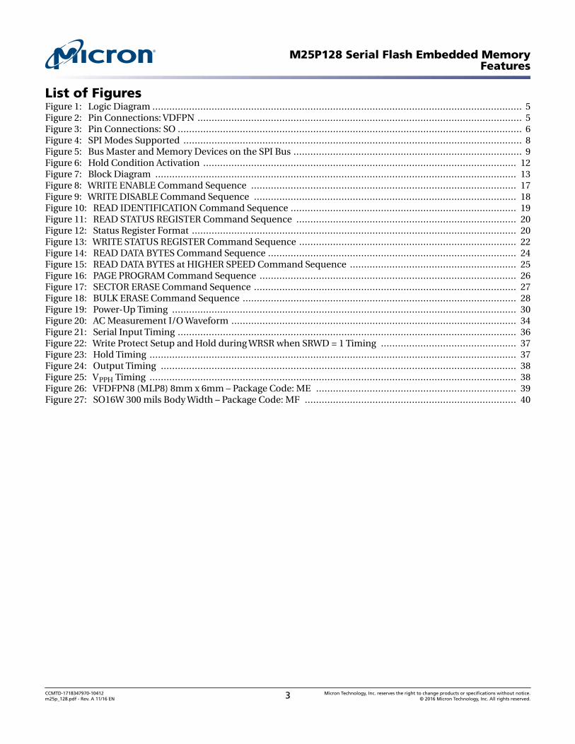
List of FiguresFigure 1: Logic Diagram ................................................................................................................................... 5Figure 2: Pin Connections: VDFPN ................................................................................................................... 5Figure 3: Pin Connections: SO .......................................................................................................................... 6Figure 4: SPI Modes Supported ........................................................................................................................ 8Figure 5: Bus Master and Memory Devices on the SPI Bus ................................................................................. 9Figure 6: Hold Condition Activation ............................................................................................................... 12Figure 7: Block Diagram ................................................................................................................................ 13Figure 8: WRITE ENABLE Command Sequence .............................................................................................. 17Figure 9: WRITE DISABLE Command Sequence ............................................................................................. 18Figure 10: READ IDENTIFICATION Command Sequence ................................................................................ 19Figure 11: READ STATUS REGISTER Command Sequence .............................................................................. 20Figure 12: Status Register Format ................................................................................................................... 20Figure 13: WRITE STATUS REGISTER Command Sequence ............................................................................. 22Figure 14: READ DATA BYTES Command Sequence ........................................................................................ 24Figure 15: READ DATA BYTES at HIGHER SPEED Command Sequence ........................................................... 25Figure 16: PAGE PROGRAM Command Sequence ........................................................................................... 26Figure 17: SECTOR ERASE Command Sequence ............................................................................................. 27Figure 18: BULK ERASE Command Sequence ................................................................................................. 28Figure 19: Power-Up Timing .......................................................................................................................... 30Figure 20: AC Measurement I/O Waveform ..................................................................................................... 34Figure 21: Serial Input Timing ........................................................................................................................ 36Figure 22: Write Protect Setup and Hold during WRSR when SRWD = 1 Timing ................................................ 37Figure 23: Hold Timing .................................................................................................................................. 37Figure 24: Output Timing .............................................................................................................................. 38Figure 25: VPPH Timing .................................................................................................................................. 38Figure 26: VFDFPN8 (MLP8) 8mm x 6mm – Package Code: ME ....................................................................... 39Figure 27: SO16W 300 mils Body Width – Package Code: MF ........................................................................... 40
M25P128 Serial Flash Embedded MemoryFeatures
CCMTD-1718347970-10412m25p_128.pdf - Rev. A 11/16 EN 3 Micron Technology, Inc. reserves the right to change products or specifications without notice.
© 2016 Micron Technology, Inc. All rights reserved.
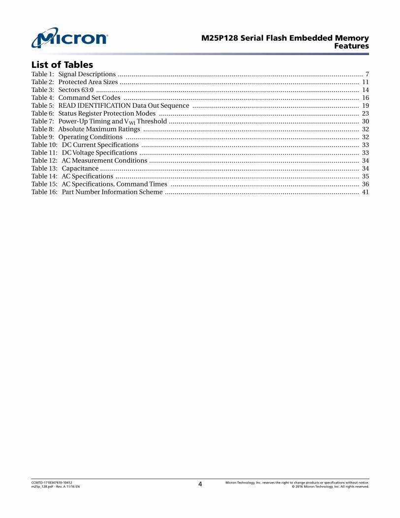
List of TablesTable 1: Signal Descriptions ............................................................................................................................. 7Table 2: Protected Area Sizes .......................................................................................................................... 11Table 3: Sectors 63:0 ...................................................................................................................................... 14Table 4: Command Set Codes ........................................................................................................................ 16Table 5: READ IDENTIFICATION Data Out Sequence ..................................................................................... 19Table 6: Status Register Protection Modes ...................................................................................................... 23Table 7: Power-Up Timing and VWI Threshold ................................................................................................. 30Table 8: Absolute Maximum Ratings .............................................................................................................. 32Table 9: Operating Conditions ....................................................................................................................... 32Table 10: DC Current Specifications ............................................................................................................... 33Table 11: DC Voltage Specifications ................................................................................................................ 33Table 12: AC Measurement Conditions ........................................................................................................... 34Table 13: Capacitance .................................................................................................................................... 34Table 14: AC Specifications ............................................................................................................................ 35Table 15: AC Specifications, Command Times ................................................................................................ 36Table 16: Part Number Information Scheme ................................................................................................... 41
M25P128 Serial Flash Embedded MemoryFeatures
CCMTD-1718347970-10412m25p_128.pdf - Rev. A 11/16 EN 4 Micron Technology, Inc. reserves the right to change products or specifications without notice.
© 2016 Micron Technology, Inc. All rights reserved.
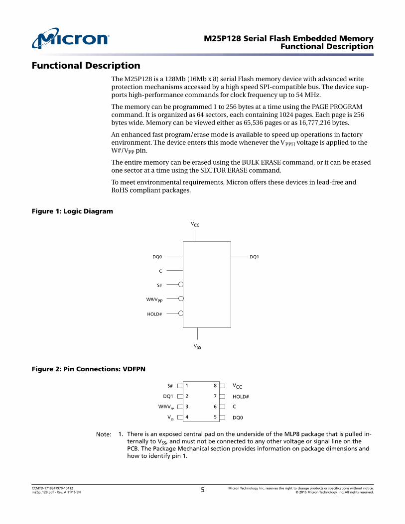
Functional DescriptionThe M25P128 is a 128Mb (16Mb x 8) serial Flash memory device with advanced writeprotection mechanisms accessed by a high speed SPI-compatible bus. The device sup-ports high-performance commands for clock frequency up to 54 MHz.
The memory can be programmed 1 to 256 bytes at a time using the PAGE PROGRAMcommand. It is organized as 64 sectors, each containing 1024 pages. Each page is 256bytes wide. Memory can be viewed either as 65,536 pages or as 16,777,216 bytes.
An enhanced fast program/erase mode is available to speed up operations in factoryenvironment. The device enters this mode whenever the VPPH voltage is applied to theW#/VPP pin.
The entire memory can be erased using the BULK ERASE command, or it can be erasedone sector at a time using the SECTOR ERASE command.
To meet environmental requirements, Micron offers these devices in lead-free andRoHS compliant packages.
Figure 1: Logic Diagram
S#
VCC
HOLD#
VSS
DQ1
C
DQ0
W#/VPP
Figure 2: Pin Connections: VDFPN
1
2
3
4
VCC
HOLD#
5
6
7
8
DQ1
VSS
S#
DQ0
C W#/VPP
Note: 1. There is an exposed central pad on the underside of the MLP8 package that is pulled in-ternally to VSS, and must not be connected to any other voltage or signal line on thePCB. The Package Mechanical section provides information on package dimensions andhow to identify pin 1.
M25P128 Serial Flash Embedded MemoryFunctional Description
CCMTD-1718347970-10412m25p_128.pdf - Rev. A 11/16 EN 5 Micron Technology, Inc. reserves the right to change products or specifications without notice.
© 2016 Micron Technology, Inc. All rights reserved.
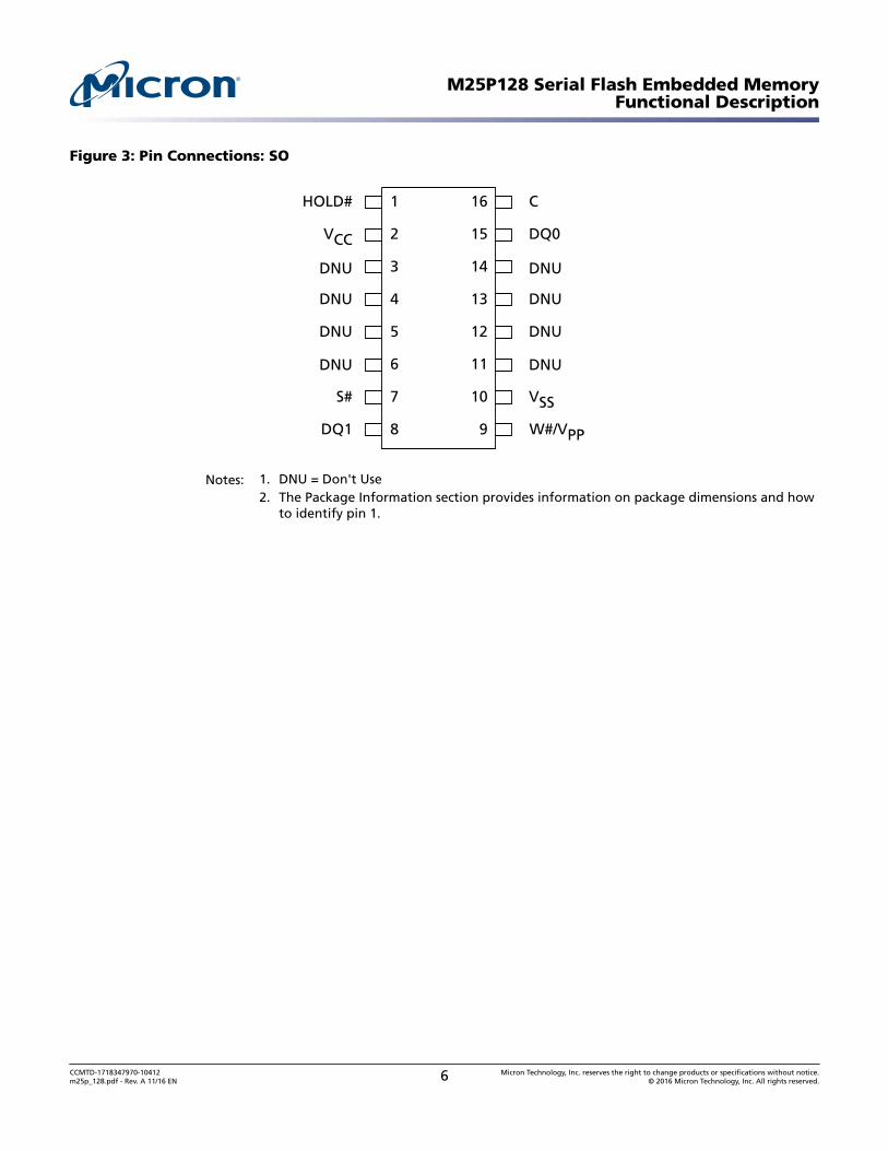
Figure 3: Pin Connections: SO
1
2
3
4
16
15
14
13
VCC
HOLD#
DNU
DNU
DNU
DNU
DNU
DNU
DNU
DNU
5
6
7
8
12
11
10
9DQ1
VSSS#
DQ0
C
W#/VPP
Notes: 1. DNU = Don't Use2. The Package Information section provides information on package dimensions and how
to identify pin 1.
M25P128 Serial Flash Embedded MemoryFunctional Description
CCMTD-1718347970-10412m25p_128.pdf - Rev. A 11/16 EN 6 Micron Technology, Inc. reserves the right to change products or specifications without notice.
© 2016 Micron Technology, Inc. All rights reserved.
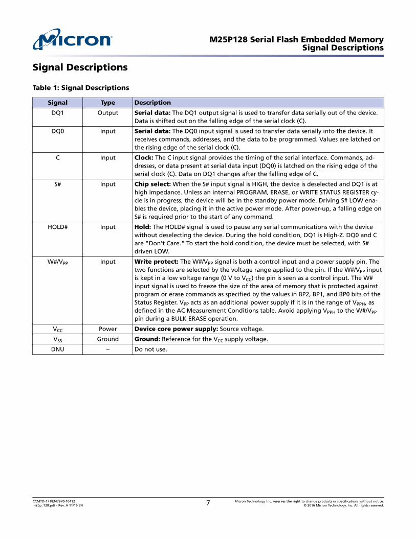
Signal Descriptions
Table 1: Signal Descriptions
Signal Type Description
DQ1 Output Serial data: The DQ1 output signal is used to transfer data serially out of the device.Data is shifted out on the falling edge of the serial clock (C).
DQ0 Input Serial data: The DQ0 input signal is used to transfer data serially into the device. Itreceives commands, addresses, and the data to be programmed. Values are latched onthe rising edge of the serial clock (C).
C Input Clock: The C input signal provides the timing of the serial interface. Commands, ad-dresses, or data present at serial data input (DQ0) is latched on the rising edge of theserial clock (C). Data on DQ1 changes after the falling edge of C.
S# Input Chip select: When the S# input signal is HIGH, the device is deselected and DQ1 is athigh impedance. Unless an internal PROGRAM, ERASE, or WRITE STATUS REGISTER cy-cle is in progress, the device will be in the standby power mode. Driving S# LOW ena-bles the device, placing it in the active power mode. After power-up, a falling edge onS# is required prior to the start of any command.
HOLD# Input Hold: The HOLD# signal is used to pause any serial communications with the devicewithout deselecting the device. During the hold condition, DQ1 is High-Z. DQ0 and Care "Don’t Care." To start the hold condition, the device must be selected, with S#driven LOW.
W#/VPP Input Write protect: The W#/VPP signal is both a control input and a power supply pin. Thetwo functions are selected by the voltage range applied to the pin. If the W#/VPP inputis kept in a low voltage range (0 V to VCC) the pin is seen as a control input. The W#input signal is used to freeze the size of the area of memory that is protected againstprogram or erase commands as specified by the values in BP2, BP1, and BP0 bits of theStatus Register. VPP acts as an additional power supply if it is in the range of VPPH, asdefined in the AC Measurement Conditions table. Avoid applying VPPH to the W#/VPP
pin during a BULK ERASE operation.
VCC Power Device core power supply: Source voltage.
VSS Ground Ground: Reference for the VCC supply voltage.
DNU – Do not use.
M25P128 Serial Flash Embedded MemorySignal Descriptions
CCMTD-1718347970-10412m25p_128.pdf - Rev. A 11/16 EN 7 Micron Technology, Inc. reserves the right to change products or specifications without notice.
© 2016 Micron Technology, Inc. All rights reserved.
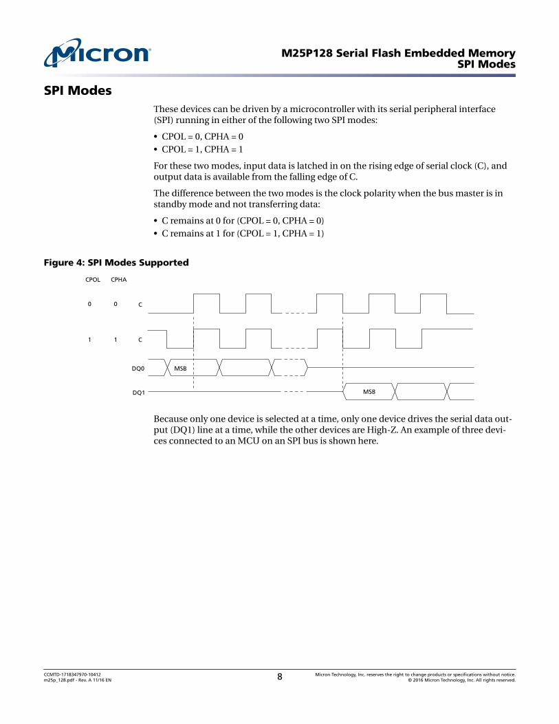
SPI ModesThese devices can be driven by a microcontroller with its serial peripheral interface(SPI) running in either of the following two SPI modes:
• CPOL = 0, CPHA = 0• CPOL = 1, CPHA = 1
For these two modes, input data is latched in on the rising edge of serial clock (C), andoutput data is available from the falling edge of C.
The difference between the two modes is the clock polarity when the bus master is instandby mode and not transferring data:
• C remains at 0 for (CPOL = 0, CPHA = 0)• C remains at 1 for (CPOL = 1, CPHA = 1)
Figure 4: SPI Modes Supported
C
MSB
CPHA
DQ0
0
1
CPOL
0
1
DQ1
C
MSB
Because only one device is selected at a time, only one device drives the serial data out-put (DQ1) line at a time, while the other devices are High-Z. An example of three devi-ces connected to an MCU on an SPI bus is shown here.
M25P128 Serial Flash Embedded MemorySPI Modes
CCMTD-1718347970-10412m25p_128.pdf - Rev. A 11/16 EN 8 Micron Technology, Inc. reserves the right to change products or specifications without notice.
© 2016 Micron Technology, Inc. All rights reserved.
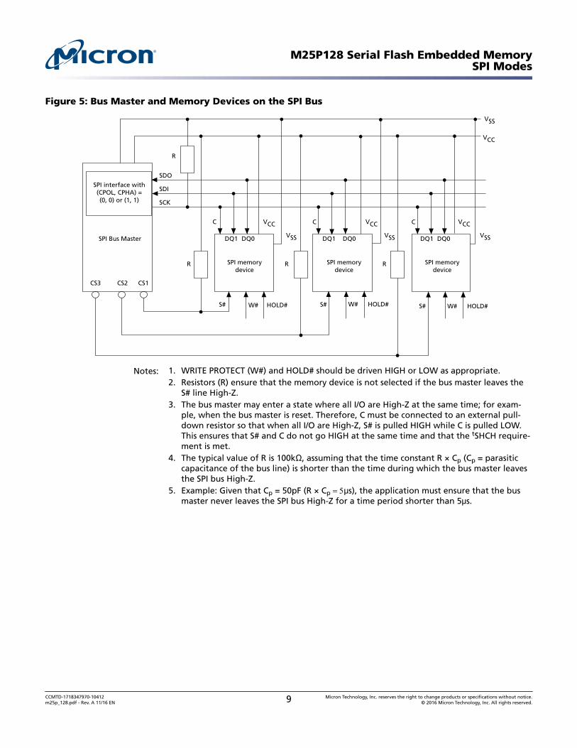
Figure 5: Bus Master and Memory Devices on the SPI Bus
SPI Bus Master
SPI memorydevice
SDO
SDI
SCK
C
DQ1 DQ0
S#
SPI memorydevice
C
DQ1 DQ0
S#
SPI memorydevice
C
DQ1 DQ0
S#
CS3 CS2 CS1
SPI interface with(CPOL, CPHA) =(0, 0) or (1, 1)
W# HOLD# HOLD# W# HOLD#
R R R
VCC
VCC VCC VCC
VSS
VSS VSS VSS
R
W#
Notes: 1. WRITE PROTECT (W#) and HOLD# should be driven HIGH or LOW as appropriate.2. Resistors (R) ensure that the memory device is not selected if the bus master leaves the
S# line High-Z.3. The bus master may enter a state where all I/O are High-Z at the same time; for exam-
ple, when the bus master is reset. Therefore, C must be connected to an external pull-down resistor so that when all I/O are High-Z, S# is pulled HIGH while C is pulled LOW.This ensures that S# and C do not go HIGH at the same time and that the tSHCH require-ment is met.
4. The typical value of R is 100kΩ, assuming that the time constant R × Cp (Cp = parasiticcapacitance of the bus line) is shorter than the time during which the bus master leavesthe SPI bus High-Z.
5. Example: Given that Cp = 50pF (R × Cp = 5μs), the application must ensure that the busmaster never leaves the SPI bus High-Z for a time period shorter than 5μs.
M25P128 Serial Flash Embedded MemorySPI Modes
CCMTD-1718347970-10412m25p_128.pdf - Rev. A 11/16 EN 9 Micron Technology, Inc. reserves the right to change products or specifications without notice.
© 2016 Micron Technology, Inc. All rights reserved.
Operating Features
Page Programming
To program one data byte, two commands are required: WRITE ENABLE, which is onebyte, and a PAGE PROGRAM sequence, which is four bytes plus data. This is followed bythe internal PROGRAM cycle of duration tPP. To spread this overhead, the PAGE PRO-GRAM command allows up to 256 bytes to be programmed at a time (changing bitsfrom 1 to 0), provided they lie in consecutive addresses on the same page of memory. Tooptimize timings, it is recommended to use the PAGE PROGRAM command to programall consecutive targeted bytes in a single sequence than to use several PAGE PROGRAMsequences with each containing only a few bytes.
Sector Erase, Bulk Erase
The PAGE PROGRAM command allows bits to be reset from 1 to 0. Before this can beapplied, the bytes of memory need to have been erased to all 1s (FFh). This can be ach-ieved a sector at a time using the SECTOR ERASE command, or throughout the entirememory using the BULK ERASE command. This starts an internal ERASE cycle of dura-tion tSSE, tSE, or tBE. The ERASE command must be preceded by a WRITE ENABLEcommand.
Polling during a Write, Program, or Erase Cycle
An improvement in the time to complete the following commands can be achieved bynot waiting for the worst case delay (tW, tPP, tSE, or tBE).
• WRITE STATUS REGISTER• PROGRAM• ERASE (SECTOR ERASE, BULK ERASE)
The write in progress (WIP) bit is provided in the status register so that the applicationprogram can monitor this bit in the status register, polling it to establish when the pre-vious WRITE cycle, PROGRAM cycle, or ERASE cycle is complete.
Fast Program/Erase Mode
The fast program/erase mode is used to speed up programming/erasing. The device en-ters this mode during the PAGE PROGRAM, SECTOR ERASE, or BULK ERASE operationswhenever a voltage equal to VPPH is applied to the W#/VPP pin.
The use of this mode requires specific operating conditions in addition to the normalones (VCC must be within the normal operating range):
• The voltage applied to the W#/VPP pin must be equal to VPPH
• Ambient temperature, TA must be 25 °C ±10 °C• The cumulated time during which W#/VPP is at VPPH should be less than 80 hours
Active Power and Standby Power
When chip select (S#) is LOW, the device is selected, and in the active power mode.When S# is HIGH, the device is deselected, but could remain in the active power modeuntil all internal cycles have completed (PROGRAM, ERASE, WRITE STATUS REGIS-
M25P128 Serial Flash Embedded MemoryOperating Features
CCMTD-1718347970-10412m25p_128.pdf - Rev. A 11/16 EN 10 Micron Technology, Inc. reserves the right to change products or specifications without notice.
© 2016 Micron Technology, Inc. All rights reserved.
TER). The device then goes in to the standby power mode. The device consumptiondrops to ICC1.
Status Register
The status register contains a number of status and control bits that can be read or set(as appropriate) by specific commands. For a detailed description of the status registerbits, see READ STATUS REGISTER section.
Data Protection by Protocol
Nonvolatile memory is used in environments that can include excessive noise. The fol-lowing capabilities help protect data in these noisy environments.
Power on reset and an internal timer (tPUW) can provide protection against inadvertentchanges while the power supply is outside the operating specification.
WRITE, PROGRAM, and WRITE STATUS REGISTER commands are checked before theyare accepted for execution to ensure they consist of a number of clock pulses that is amultiple of eight.
All commands that modify data must be preceded by a WRITE ENABLE command to setthe write enable latch (WEL) bit.
Software Data Protection
Memory can be configured as read-only using the block protect bits (BP2, BP1, BP0) asshown in the Protected Area Sizes table.
Hardware Data Protection
Hardware data protection is implemented using the write protect signal applied on theW# pin. This freezes the status register in a read-only mode. In this mode, the block pro-tect (BP) bits and the status register write disable bit (SRWD) are protected.
Table 2: Protected Area Sizes
Status Register Content Memory Content
BP Bit 2 BP Bit 1 BP Bit 0 Protected Area Unprotected Area
0 0 0 none All sectors (sectors 0 to 63)
0 0 1 Upper 64th (sector 63, 2Mb) Lower 63/64ths (sectors 0 to 62)
0 1 0 Upper 32nd (sectors 62 and 63, 4Mb) Lower 31/32nds (sectors 0 to 61)
0 1 1 Upper 16th (sectors 60 and 63, 8Mb) Lower 15/16ths (sectors 0 to 59)
1 0 0 Upper 8th (sectors 56 to 63, 16Mb) Lower 7/8ths (sectors 0 to 55)
1 0 1 Upper 4th (sectors 48 to 63, 32Mb) Lower 3/4ths (sectors 0 to 47)
1 1 0 Upper half (sectors 32 to 63, 64Mb) Lower half (sectors 0 to 31)
1 1 1 All sectors (sectors 0 to 63, 128Mb) none
Note: 1. 0 0 0 = unprotected area (sectors): The device is ready to accept a BULK ERASE commandonly if all block protect bits (BP2, BP1, BP0) are 0.
M25P128 Serial Flash Embedded MemoryOperating Features
CCMTD-1718347970-10412m25p_128.pdf - Rev. A 11/16 EN 11 Micron Technology, Inc. reserves the right to change products or specifications without notice.
© 2016 Micron Technology, Inc. All rights reserved.
Hold Condition
The HOLD# signal is used to pause any serial communications with the device withoutresetting the clocking sequence. However, taking this signal LOW does not terminateany WRITE STATUS REGISTER, PROGRAM, or ERASE cycle that is currently in progress.
To enter the hold condition, the device must be selected, with S# LOW. The hold condi-tion starts on the falling edge of the HOLD# signal, if this coincides with serial clock (C)being LOW. The hold condition ends on the rising edge of the HOLD# signal, if this co-incides with C being LOW. If the falling edge does not coincide with C being LOW, thehold condition starts after C next goes LOW. Similarly, if the rising edge does not coin-cide with C being LOW, the hold condition ends after C next goes LOW.
During the hold condition, DQ1 is HIGH impedance while DQ0 and C are "Don’t Care."Typically, the device remains selected with S# driven LOW for the duration of the holdcondition. This ensures that the state of the internal logic remains unchanged from themoment of entering the hold condition. If S# goes HIGH while the device is in the holdcondition, the internal logic of the device is reset. To restart communication with thedevice, it is necessary to drive HOLD# HIGH, and then to drive S# LOW. This preventsthe device from going back to the hold condition.
Figure 6: Hold Condition Activation
HOLD#
C
HOLD condition (standard use) HOLD condition (nonstandard use)
M25P128 Serial Flash Embedded MemoryOperating Features
CCMTD-1718347970-10412m25p_128.pdf - Rev. A 11/16 EN 12 Micron Technology, Inc. reserves the right to change products or specifications without notice.
© 2016 Micron Technology, Inc. All rights reserved.
Configuration and Memory Map
Memory Configuration and Block Diagram
Each page of memory can be individually programmed; bits are programmed from 1 to0. The device is sector or bulk-erasable, but not page-erasable; bits are erased from 0 to1. The memory is configured as follows:
• 16,777,216 bytes (8 bits each)• 64 sectors (2Mb, 262,144 bytes each)• 65,536 pages (256 bytes each)
Figure 7: Block Diagram
HOLD#
S#
W#/VPP Control LogicHigh Voltage
Generator
I/O Shift Register
Address Registerand Counter
256 ByteData Buffer
256 bytes (page size)
X Decoder
Y D
eco
der
C
DQ0
DQ1
StatusRegister
00000h
FFFFFFh
000FFh
64 OTP bytes
M25P128 Serial Flash Embedded MemoryConfiguration and Memory Map
CCMTD-1718347970-10412m25p_128.pdf - Rev. A 11/16 EN 13 Micron Technology, Inc. reserves the right to change products or specifications without notice.
© 2016 Micron Technology, Inc. All rights reserved.
Memory Map – 128Mb Density
Table 3: Sectors 63:0
Sector
Address Range
Start End
63 FC0000h FFFFFFh
62 F80000h FBFFFFh
⋮ ⋮ ⋮48 C00000h C3FFFFh
47 BC0000h BFFFFFh
⋮ ⋮ ⋮32 800000h 83FFFFh
31 7C0000h 7FFFFFh
⋮ ⋮ ⋮16 400000h 43FFFFh
15 3C0000h 3FFFFFh
⋮ ⋮ ⋮0 000000h 03FFFFh
M25P128 Serial Flash Embedded MemoryMemory Map – 128Mb Density
CCMTD-1718347970-10412m25p_128.pdf - Rev. A 11/16 EN 14 Micron Technology, Inc. reserves the right to change products or specifications without notice.
© 2016 Micron Technology, Inc. All rights reserved.
Command Set OverviewAll commands, addresses, and data are shifted in and out of the device, most significantbit first.
Serial data inputs DQ0 and DQ1 are sampled on the first rising edge of serial clock (C)after chip select (S#) is driven LOW. Then, the one-byte command code must be shiftedin to the device, most significant bit first, on DQ0 and DQ1, each bit being latched onthe rising edges of C.
Every command sequence starts with a one-byte command code. Depending on thecommand, this command code might be followed by address or data bytes, by addressand data bytes, or by neither address or data bytes. For the following commands, theshifted-in command sequence is followed by a data-out sequence. S# can be drivenHIGH after any bit of the data-out sequence is being shifted out.
• READ DATA BYTES (READ)• READ DATA BYTES at HIGHER SPEED• READ STATUS REGISTER• READ IDENTIFICATION
For the following commands, S# must be driven HIGH exactly at a byte boundary. Thatis, after an exact multiple of eight clock pulses following S# being driven LOW, S# mustbe driven HIGH. Otherwise, the command is rejected and not executed.
• PAGE PROGRAM• SECTOR ERASE• BULK ERASE• WRITE STATUS REGISTER• WRITE ENABLE• WRITE DISABLE
All attempts to access the memory array are ignored during a WRITE STATUS REGISTERcommand cycle, a PROGRAM command cycle, or an ERASE command cycle. In addi-tion, the internal cycle for each of these commands continues unaffected.
M25P128 Serial Flash Embedded MemoryCommand Set Overview
CCMTD-1718347970-10412m25p_128.pdf - Rev. A 11/16 EN 15 Micron Technology, Inc. reserves the right to change products or specifications without notice.
© 2016 Micron Technology, Inc. All rights reserved.
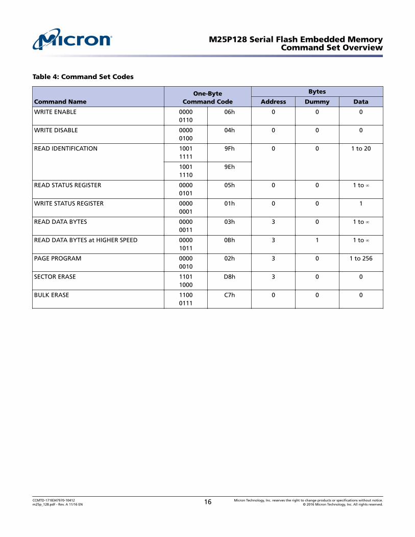
Table 4: Command Set Codes
Command NameOne-Byte
Command Code
Bytes
Address Dummy Data
WRITE ENABLE 00000110
06h 0 0 0
WRITE DISABLE 00000100
04h 0 0 0
READ IDENTIFICATION 10011111
9Fh 0 0 1 to 20
10011110
9Eh
READ STATUS REGISTER 00000101
05h 0 0 1 to ∞
WRITE STATUS REGISTER 00000001
01h 0 0 1
READ DATA BYTES 00000011
03h 3 0 1 to ∞
READ DATA BYTES at HIGHER SPEED 00001011
0Bh 3 1 1 to ∞
PAGE PROGRAM 00000010
02h 3 0 1 to 256
SECTOR ERASE 11011000
D8h 3 0 0
BULK ERASE 11000111
C7h 0 0 0
M25P128 Serial Flash Embedded MemoryCommand Set Overview
CCMTD-1718347970-10412m25p_128.pdf - Rev. A 11/16 EN 16 Micron Technology, Inc. reserves the right to change products or specifications without notice.
© 2016 Micron Technology, Inc. All rights reserved.
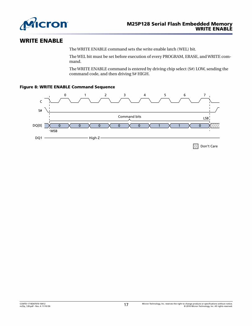
WRITE ENABLEThe WRITE ENABLE command sets the write enable latch (WEL) bit.
The WEL bit must be set before execution of every PROGRAM, ERASE, and WRITE com-mand.
The WRITE ENABLE command is entered by driving chip select (S#) LOW, sending thecommand code, and then driving S# HIGH.
Figure 8: WRITE ENABLE Command Sequence
Don’t Care
DQ[0]
0 1 2 4 53 76
C
High-ZDQ1
MSB
LSB
0 0 0 0 0 011
Command bits
S#
M25P128 Serial Flash Embedded MemoryWRITE ENABLE
CCMTD-1718347970-10412m25p_128.pdf - Rev. A 11/16 EN 17 Micron Technology, Inc. reserves the right to change products or specifications without notice.
© 2016 Micron Technology, Inc. All rights reserved.
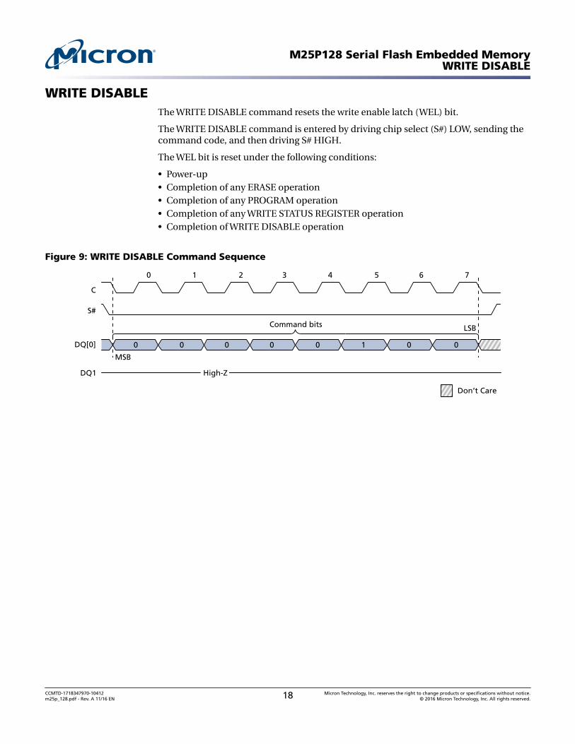
WRITE DISABLEThe WRITE DISABLE command resets the write enable latch (WEL) bit.
The WRITE DISABLE command is entered by driving chip select (S#) LOW, sending thecommand code, and then driving S# HIGH.
The WEL bit is reset under the following conditions:
• Power-up• Completion of any ERASE operation• Completion of any PROGRAM operation• Completion of any WRITE STATUS REGISTER operation• Completion of WRITE DISABLE operation
Figure 9: WRITE DISABLE Command Sequence
Don’t Care
DQ[0]
0 1 2 4 53 76
C
High-ZDQ1
MSB
LSB
0 0 0 0 0 001
Command bits
S#
M25P128 Serial Flash Embedded MemoryWRITE DISABLE
CCMTD-1718347970-10412m25p_128.pdf - Rev. A 11/16 EN 18 Micron Technology, Inc. reserves the right to change products or specifications without notice.
© 2016 Micron Technology, Inc. All rights reserved.
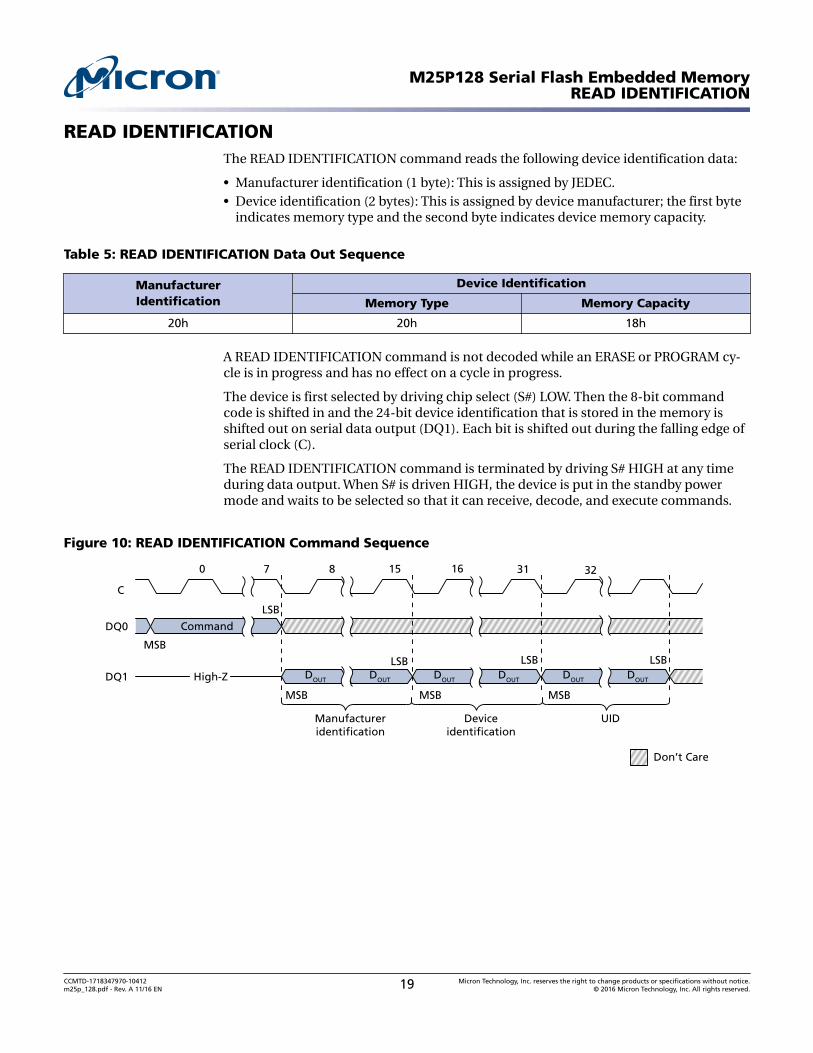
READ IDENTIFICATIONThe READ IDENTIFICATION command reads the following device identification data:
• Manufacturer identification (1 byte): This is assigned by JEDEC.• Device identification (2 bytes): This is assigned by device manufacturer; the first byte
indicates memory type and the second byte indicates device memory capacity.
Table 5: READ IDENTIFICATION Data Out Sequence
ManufacturerIdentification
Device Identification
Memory Type Memory Capacity
20h 20h 18h
A READ IDENTIFICATION command is not decoded while an ERASE or PROGRAM cy-cle is in progress and has no effect on a cycle in progress.
The device is first selected by driving chip select (S#) LOW. Then the 8-bit commandcode is shifted in and the 24-bit device identification that is stored in the memory isshifted out on serial data output (DQ1). Each bit is shifted out during the falling edge ofserial clock (C).
The READ IDENTIFICATION command is terminated by driving S# HIGH at any timeduring data output. When S# is driven HIGH, the device is put in the standby powermode and waits to be selected so that it can receive, decode, and execute commands.
Figure 10: READ IDENTIFICATION Command Sequence
UIDDeviceidentification
Manufactureridentification
High-ZDQ1
MSB MSB
DOUT DOUT DOUT DOUT
LSBLSB
7 8 15 16 32310
C
MSB
DQ0
LSB
Command
MSB
DOUT DOUT
LSB
Don’t Care
M25P128 Serial Flash Embedded MemoryREAD IDENTIFICATION
CCMTD-1718347970-10412m25p_128.pdf - Rev. A 11/16 EN 19 Micron Technology, Inc. reserves the right to change products or specifications without notice.
© 2016 Micron Technology, Inc. All rights reserved.
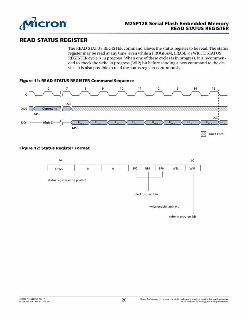
READ STATUS REGISTERThe READ STATUS REGISTER command allows the status register to be read. The statusregister may be read at any time, even while a PROGRAM, ERASE, or WRITE STATUSREGISTER cycle is in progress. When one of these cycles is in progress, it is recommen-ded to check the write in progress (WIP) bit before sending a new command to the de-vice. It is also possible to read the status register continuously.
Figure 11: READ STATUS REGISTER Command Sequence
High-ZDQ1
7 8 9 10 11 12 13 14 150
C
MSB
DQ0
LSB
Command
MSB
DOUT DOUT DOUT DOUT DOUT
LSBDOUT DOUT DOUT DOUT
Don’t Care
Figure 12: Status Register Format
b7
SRWD 0 0 BP2 BP1 BP0 WEL WIP
b0
status register write protect
block protect bits
write enable latch bit
write in progress bit
M25P128 Serial Flash Embedded MemoryREAD STATUS REGISTER
CCMTD-1718347970-10412m25p_128.pdf - Rev. A 11/16 EN 20 Micron Technology, Inc. reserves the right to change products or specifications without notice.
© 2016 Micron Technology, Inc. All rights reserved.
WIP Bit
The write in progress (WIP) bit indicates whether the memory is busy with a WRITESTATUS REGISTER cycle, a PROGRAM cycle, or an ERASE cycle. When the WIP bit is setto 1, a cycle is in progress; when the WIP bit is set to 0, a cycle is not in progress.
WEL Bit
The write enable latch (WEL) bit indicates the status of the internal write enable latch.When the WEL bit is set to 1, the internal write enable latch is set; when the WEL bit isset to 0, the internal write enable latch is reset and no WRITE STATUS REGISTER, PRO-GRAM, or ERASE command is accepted.
Block Protect Bits
The block protect bits are non-volatile. They define the size of the area to be softwareprotected against PROGRAM and ERASE commands. The block protect bits are writtenwith the WRITE STATUS REGISTER command.
When one or more of the block protect bits is set to 1, the relevant memory area, as de-fined in the Protected Area Sizes table, becomes protected against PAGE PROGRAM andSECTOR ERASE commands. The block protect bits can be written provided that thehardware protected mode has not been set. The BULK ERASE command is executed on-ly if all block protect bits are 0.
SRWD Bit
The status register write disable (SRWD) bit is operated in conjunction with the writeprotect (W#/VPP) signal. When the SRWD bit is set to 1 and W#/V PP is driven LOW, thedevice is put in the hardware protected mode. In the hardware protected mode, thenon-volatile bits of the status register (SRWD, and the block protect bits) become read-only bits and the WRITE STATUS REGISTER command is no longer accepted for execu-tion.
M25P128 Serial Flash Embedded MemoryREAD STATUS REGISTER
CCMTD-1718347970-10412m25p_128.pdf - Rev. A 11/16 EN 21 Micron Technology, Inc. reserves the right to change products or specifications without notice.
© 2016 Micron Technology, Inc. All rights reserved.
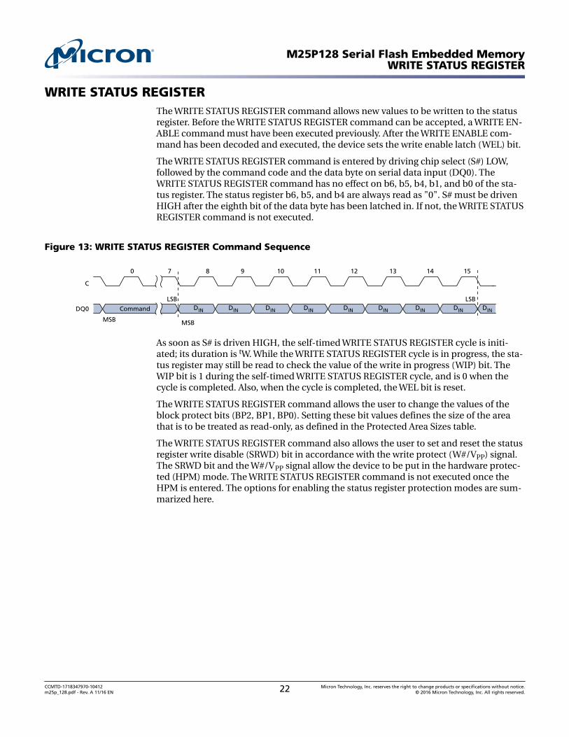
WRITE STATUS REGISTERThe WRITE STATUS REGISTER command allows new values to be written to the statusregister. Before the WRITE STATUS REGISTER command can be accepted, a WRITE EN-ABLE command must have been executed previously. After the WRITE ENABLE com-mand has been decoded and executed, the device sets the write enable latch (WEL) bit.
The WRITE STATUS REGISTER command is entered by driving chip select (S#) LOW,followed by the command code and the data byte on serial data input (DQ0). TheWRITE STATUS REGISTER command has no effect on b6, b5, b4, b1, and b0 of the sta-tus register. The status register b6, b5, and b4 are always read as "0". S# must be drivenHIGH after the eighth bit of the data byte has been latched in. If not, the WRITE STATUSREGISTER command is not executed.
Figure 13: WRITE STATUS REGISTER Command Sequence
7 8 9 10 11 12 13 14 150
C
MSB
DQ0
LSB
Command
MSB
LSBDIN DIN DIN DIN DINDIN DIN DIN DIN
As soon as S# is driven HIGH, the self-timed WRITE STATUS REGISTER cycle is initi-ated; its duration is tW. While the WRITE STATUS REGISTER cycle is in progress, the sta-tus register may still be read to check the value of the write in progress (WIP) bit. TheWIP bit is 1 during the self-timed WRITE STATUS REGISTER cycle, and is 0 when thecycle is completed. Also, when the cycle is completed, the WEL bit is reset.
The WRITE STATUS REGISTER command allows the user to change the values of theblock protect bits (BP2, BP1, BP0). Setting these bit values defines the size of the areathat is to be treated as read-only, as defined in the Protected Area Sizes table.
The WRITE STATUS REGISTER command also allows the user to set and reset the statusregister write disable (SRWD) bit in accordance with the write protect (W#/VPP) signal.The SRWD bit and the W#/VPP signal allow the device to be put in the hardware protec-ted (HPM) mode. The WRITE STATUS REGISTER command is not executed once theHPM is entered. The options for enabling the status register protection modes are sum-marized here.
M25P128 Serial Flash Embedded MemoryWRITE STATUS REGISTER
CCMTD-1718347970-10412m25p_128.pdf - Rev. A 11/16 EN 22 Micron Technology, Inc. reserves the right to change products or specifications without notice.
© 2016 Micron Technology, Inc. All rights reserved.
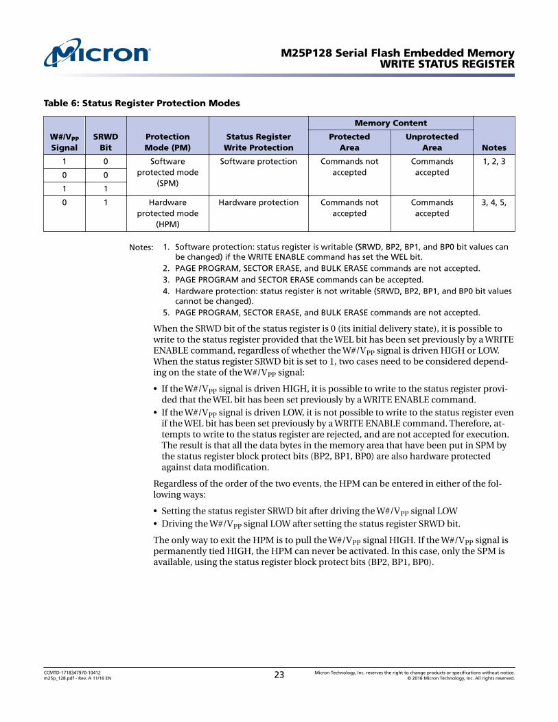
Table 6: Status Register Protection Modes
W#/VPP
SignalSRWD
BitProtectionMode (PM)
Status RegisterWrite Protection
Memory Content
NotesProtected
AreaUnprotected
Area
1 0 Softwareprotected mode
(SPM)
Software protection Commands notaccepted
Commandsaccepted
1, 2, 3
0 0
1 1
0 1 Hardwareprotected mode
(HPM)
Hardware protection Commands notaccepted
Commandsaccepted
3, 4, 5,
Notes: 1. Software protection: status register is writable (SRWD, BP2, BP1, and BP0 bit values canbe changed) if the WRITE ENABLE command has set the WEL bit.
2. PAGE PROGRAM, SECTOR ERASE, and BULK ERASE commands are not accepted.3. PAGE PROGRAM and SECTOR ERASE commands can be accepted.4. Hardware protection: status register is not writable (SRWD, BP2, BP1, and BP0 bit values
cannot be changed).5. PAGE PROGRAM, SECTOR ERASE, and BULK ERASE commands are not accepted.
When the SRWD bit of the status register is 0 (its initial delivery state), it is possible towrite to the status register provided that the WEL bit has been set previously by a WRITEENABLE command, regardless of whether the W#/VPP signal is driven HIGH or LOW.When the status register SRWD bit is set to 1, two cases need to be considered depend-ing on the state of the W#/VPP signal:
• If the W#/VPP signal is driven HIGH, it is possible to write to the status register provi-ded that the WEL bit has been set previously by a WRITE ENABLE command.
• If the W#/VPP signal is driven LOW, it is not possible to write to the status register evenif the WEL bit has been set previously by a WRITE ENABLE command. Therefore, at-tempts to write to the status register are rejected, and are not accepted for execution.The result is that all the data bytes in the memory area that have been put in SPM bythe status register block protect bits (BP2, BP1, BP0) are also hardware protectedagainst data modification.
Regardless of the order of the two events, the HPM can be entered in either of the fol-lowing ways:
• Setting the status register SRWD bit after driving the W#/VPP signal LOW• Driving the W#/VPP signal LOW after setting the status register SRWD bit.
The only way to exit the HPM is to pull the W#/VPP signal HIGH. If the W#/VPP signal ispermanently tied HIGH, the HPM can never be activated. In this case, only the SPM isavailable, using the status register block protect bits (BP2, BP1, BP0).
M25P128 Serial Flash Embedded MemoryWRITE STATUS REGISTER
CCMTD-1718347970-10412m25p_128.pdf - Rev. A 11/16 EN 23 Micron Technology, Inc. reserves the right to change products or specifications without notice.
© 2016 Micron Technology, Inc. All rights reserved.
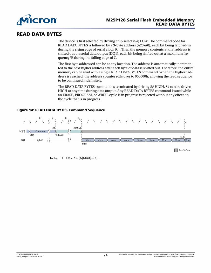
READ DATA BYTESThe device is first selected by driving chip select (S#) LOW. The command code forREAD DATA BYTES is followed by a 3-byte address (A23-A0), each bit being latched-induring the rising edge of serial clock (C). Then the memory contents at that address isshifted out on serial data output (DQ1), each bit being shifted out at a maximum fre-quency fR during the falling edge of C.
The first byte addressed can be at any location. The address is automatically incremen-ted to the next higher address after each byte of data is shifted out. Therefore, the entirememory can be read with a single READ DATA BYTES command. When the highest ad-dress is reached, the address counter rolls over to 000000h, allowing the read sequenceto be continued indefinitely.
The READ DATA BYTES command is terminated by driving S# HIGH. S# can be drivenHIGH at any time during data output. Any READ DATA BYTES command issued whilean ERASE, PROGRAM, or WRITE cycle is in progress is rejected without any effect onthe cycle that is in progress.
Figure 14: READ DATA BYTES Command Sequence
Don’t Care
MSB
DQ[0]
LSB
Command
A[MAX]
A[MIN]
7 8 Cx0
C
High-ZDQ1
MSB
DOUT DOUT DOUT DOUT DOUT
LSBDOUT DOUT DOUT DOUT
Note: 1. Cx = 7 + (A[MAX] + 1).
M25P128 Serial Flash Embedded MemoryREAD DATA BYTES
CCMTD-1718347970-10412m25p_128.pdf - Rev. A 11/16 EN 24 Micron Technology, Inc. reserves the right to change products or specifications without notice.
© 2016 Micron Technology, Inc. All rights reserved.
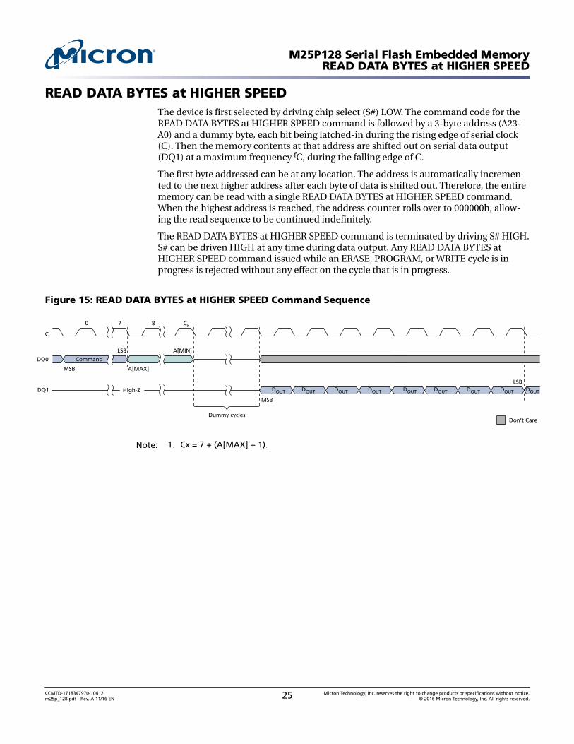
READ DATA BYTES at HIGHER SPEEDThe device is first selected by driving chip select (S#) LOW. The command code for theREAD DATA BYTES at HIGHER SPEED command is followed by a 3-byte address (A23-A0) and a dummy byte, each bit being latched-in during the rising edge of serial clock(C). Then the memory contents at that address are shifted out on serial data output(DQ1) at a maximum frequency fC, during the falling edge of C.
The first byte addressed can be at any location. The address is automatically incremen-ted to the next higher address after each byte of data is shifted out. Therefore, the entirememory can be read with a single READ DATA BYTES at HIGHER SPEED command.When the highest address is reached, the address counter rolls over to 000000h, allow-ing the read sequence to be continued indefinitely.
The READ DATA BYTES at HIGHER SPEED command is terminated by driving S# HIGH.S# can be driven HIGH at any time during data output. Any READ DATA BYTES atHIGHER SPEED command issued while an ERASE, PROGRAM, or WRITE cycle is inprogress is rejected without any effect on the cycle that is in progress.
Figure 15: READ DATA BYTES at HIGHER SPEED Command Sequence
7 8 Cx0
C
MSB
DQ0
LSB
Command
A[MAX]
A[MIN]
MSB
DOUT DOUT DOUT DOUT DOUT
LSBDOUT DOUT DOUT DOUT
Dummy cycles
DQ1 High-Z
Don’t Care
Note: 1. Cx = 7 + (A[MAX] + 1).
M25P128 Serial Flash Embedded MemoryREAD DATA BYTES at HIGHER SPEED
CCMTD-1718347970-10412m25p_128.pdf - Rev. A 11/16 EN 25 Micron Technology, Inc. reserves the right to change products or specifications without notice.
© 2016 Micron Technology, Inc. All rights reserved.
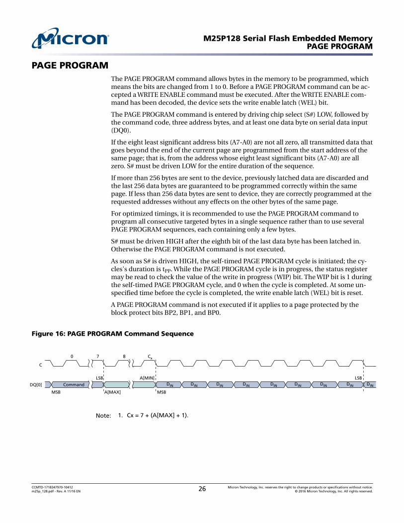
PAGE PROGRAMThe PAGE PROGRAM command allows bytes in the memory to be programmed, whichmeans the bits are changed from 1 to 0. Before a PAGE PROGRAM command can be ac-cepted a WRITE ENABLE command must be executed. After the WRITE ENABLE com-mand has been decoded, the device sets the write enable latch (WEL) bit.
The PAGE PROGRAM command is entered by driving chip select (S#) LOW, followed bythe command code, three address bytes, and at least one data byte on serial data input(DQ0).
If the eight least significant address bits (A7-A0) are not all zero, all transmitted data thatgoes beyond the end of the current page are programmed from the start address of thesame page; that is, from the address whose eight least significant bits (A7-A0) are allzero. S# must be driven LOW for the entire duration of the sequence.
If more than 256 bytes are sent to the device, previously latched data are discarded andthe last 256 data bytes are guaranteed to be programmed correctly within the samepage. If less than 256 data bytes are sent to device, they are correctly programmed at therequested addresses without any effects on the other bytes of the same page.
For optimized timings, it is recommended to use the PAGE PROGRAM command toprogram all consecutive targeted bytes in a single sequence rather than to use severalPAGE PROGRAM sequences, each containing only a few bytes.
S# must be driven HIGH after the eighth bit of the last data byte has been latched in.Otherwise the PAGE PROGRAM command is not executed.
As soon as S# is driven HIGH, the self-timed PAGE PROGRAM cycle is initiated; the cy-cles's duration is tPP. While the PAGE PROGRAM cycle is in progress, the status registermay be read to check the value of the write in progress (WIP) bit. The WIP bit is 1 duringthe self-timed PAGE PROGRAM cycle, and 0 when the cycle is completed. At some un-specified time before the cycle is completed, the write enable latch (WEL) bit is reset.
A PAGE PROGRAM command is not executed if it applies to a page protected by theblock protect bits BP2, BP1, and BP0.
Figure 16: PAGE PROGRAM Command Sequence
7 8 Cx0
C
MSB
DQ[0]
LSB
Command
A[MAX]
A[MIN]
MSB
DIN DIN DIN DIN DIN
LSBDIN DIN DIN DIN
Note: 1. Cx = 7 + (A[MAX] + 1).
M25P128 Serial Flash Embedded MemoryPAGE PROGRAM
CCMTD-1718347970-10412m25p_128.pdf - Rev. A 11/16 EN 26 Micron Technology, Inc. reserves the right to change products or specifications without notice.
© 2016 Micron Technology, Inc. All rights reserved.
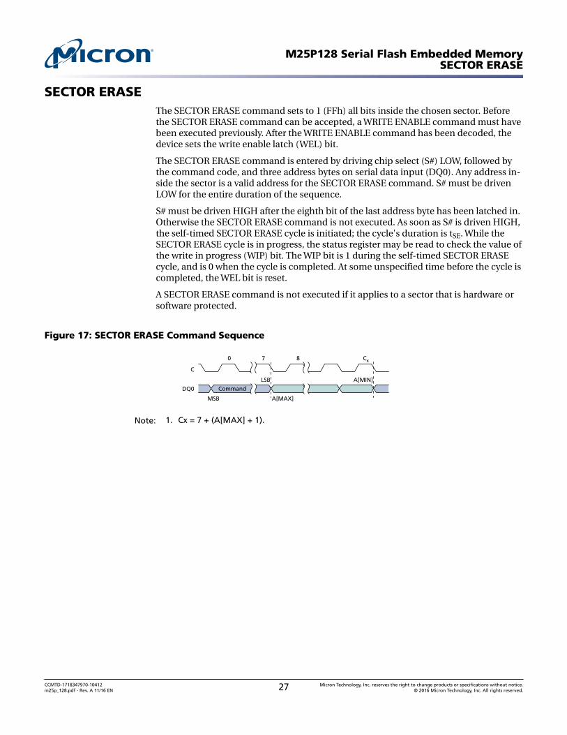
SECTOR ERASEThe SECTOR ERASE command sets to 1 (FFh) all bits inside the chosen sector. Beforethe SECTOR ERASE command can be accepted, a WRITE ENABLE command must havebeen executed previously. After the WRITE ENABLE command has been decoded, thedevice sets the write enable latch (WEL) bit.
The SECTOR ERASE command is entered by driving chip select (S#) LOW, followed bythe command code, and three address bytes on serial data input (DQ0). Any address in-side the sector is a valid address for the SECTOR ERASE command. S# must be drivenLOW for the entire duration of the sequence.
S# must be driven HIGH after the eighth bit of the last address byte has been latched in.Otherwise the SECTOR ERASE command is not executed. As soon as S# is driven HIGH,the self-timed SECTOR ERASE cycle is initiated; the cycle's duration is tSE. While theSECTOR ERASE cycle is in progress, the status register may be read to check the value ofthe write in progress (WIP) bit. The WIP bit is 1 during the self-timed SECTOR ERASEcycle, and is 0 when the cycle is completed. At some unspecified time before the cycle iscompleted, the WEL bit is reset.
A SECTOR ERASE command is not executed if it applies to a sector that is hardware orsoftware protected.
Figure 17: SECTOR ERASE Command Sequence
7 8 Cx0
C
MSB
DQ0
LSB
Command
A[MAX]
A[MIN]
Note: 1. Cx = 7 + (A[MAX] + 1).
M25P128 Serial Flash Embedded MemorySECTOR ERASE
CCMTD-1718347970-10412m25p_128.pdf - Rev. A 11/16 EN 27 Micron Technology, Inc. reserves the right to change products or specifications without notice.
© 2016 Micron Technology, Inc. All rights reserved.
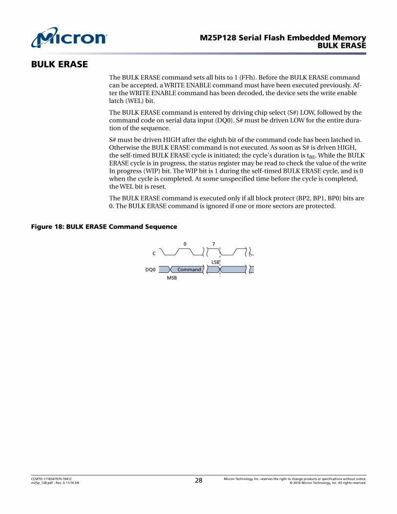
BULK ERASEThe BULK ERASE command sets all bits to 1 (FFh). Before the BULK ERASE commandcan be accepted, a WRITE ENABLE command must have been executed previously. Af-ter the WRITE ENABLE command has been decoded, the device sets the write enablelatch (WEL) bit.
The BULK ERASE command is entered by driving chip select (S#) LOW, followed by thecommand code on serial data input (DQ0). S# must be driven LOW for the entire dura-tion of the sequence.
S# must be driven HIGH after the eighth bit of the command code has been latched in.Otherwise the BULK ERASE command is not executed. As soon as S# is driven HIGH,the self-timed BULK ERASE cycle is initiated; the cycle's duration is tBE. While the BULKERASE cycle is in progress, the status register may be read to check the value of the writeIn progress (WIP) bit. The WIP bit is 1 during the self-timed BULK ERASE cycle, and is 0when the cycle is completed. At some unspecified time before the cycle is completed,the WEL bit is reset.
The BULK ERASE command is executed only if all block protect (BP2, BP1, BP0) bits are0. The BULK ERASE command is ignored if one or more sectors are protected.
Figure 18: BULK ERASE Command Sequence
70
C
MSB
DQ0
LSB
Command
M25P128 Serial Flash Embedded MemoryBULK ERASE
CCMTD-1718347970-10412m25p_128.pdf - Rev. A 11/16 EN 28 Micron Technology, Inc. reserves the right to change products or specifications without notice.
© 2016 Micron Technology, Inc. All rights reserved.
Power-Up/Down and Supply Line DecouplingAt power-up and power-down, the device must not be selected; that is, chip select (S#)must follow the voltage applied on VCC until VCC reaches the correct value:
• VCC,min at power-up, and then for a further delay of tVSL• VSS at power-down
A safe configuration is provided in the SPI Modes section.
To avoid data corruption and inadvertent WRITE operations during power-up, a power-on-reset (POR) circuit is included. The logic inside the device is held reset while VCC isless than the POR threshold voltage, VWI – all operations are disabled, and the devicedoes not respond to any instruction. Moreover, the device ignores the following instruc-tions until a time delay of tPUW has elapsed after the moment that VCC rises above theVWI threshold:
• WRITE ENABLE• PAGE PROGRAM• SECTOR ERASE• BULK ERASE• WRITE STATUS REGISTER
However, the correct operation of the device is not guaranteed if, by this time, VCC is stillbelow VCC.min. No WRITE STATUS REGISTER, PROGRAM, or ERASE instruction shouldbe sent until:
• tPUW after VCC has passed the VWI threshold• tVSL after VCC has passed the VCC,min level
If the time, tVSL, has elapsed, after VCC rises above VCC,min, the device can be selectedfor READ instructions even if the tPUW delay has not yet fully elapsed.
VPPH must be applied only when VCC is stable and in the VCC,min to VCC,max voltagerange.
M25P128 Serial Flash Embedded MemoryPower-Up/Down and Supply Line Decoupling
CCMTD-1718347970-10412m25p_128.pdf - Rev. A 11/16 EN 29 Micron Technology, Inc. reserves the right to change products or specifications without notice.
© 2016 Micron Technology, Inc. All rights reserved.
Figure 19: Power-Up Timing
VCC
VCC,min
VWI
RESET stateof thedevice
Chip selection not allowed
PROGRAM, ERASE, and WRITE commands are rejected by the device
tVSL
tPUW
Time
READ access allowed Device fullyaccessible
VCC,max
After power-up, the device is in the following state:
• Standby power mode• Write enable latch (WEL) bit is reset
Normal precautions must be taken for supply line decoupling to stabilize the VCC sup-ply. Each device in a system should have the VCC line decoupled by a suitable capacitorclose to the package pins; generally, this capacitor is of the order of 0.1µF.
At power-down, when VCC drops from the operating voltage to below the POR thresholdvoltage VWI, all operations are disabled and the device does not respond to any instruc-tion.
Note: If power-down occurs while a WRITE, PROGRAM, or ERASE cycle is in progress,some data corruption may result.
Power-Up Timing and Write Inhibit Voltage Threshold Specifications
Table 7: Power-Up Timing and VWI Threshold
Symbol Parameter Min Max UnittVSL VCC,min to S# LOW 200 – μs
tPUW Time delay to WRITE instruction 400 – μs
VWI Write Inhibit voltage 1.5 2.5 V
Note: 1. Parameters are characterized only.
M25P128 Serial Flash Embedded MemoryPower-Up Timing and Write Inhibit Voltage Threshold Specifi-
cations
CCMTD-1718347970-10412m25p_128.pdf - Rev. A 11/16 EN 30 Micron Technology, Inc. reserves the right to change products or specifications without notice.
© 2016 Micron Technology, Inc. All rights reserved.
Initial Delivery StatusThe device is delivered as the following:
• Memory array erased: all bits are set to 1 (each byte contains FFh)• Status register contains 00h (all status register bits are 0)
M25P128 Serial Flash Embedded MemoryInitial Delivery Status
CCMTD-1718347970-10412m25p_128.pdf - Rev. A 11/16 EN 31 Micron Technology, Inc. reserves the right to change products or specifications without notice.
© 2016 Micron Technology, Inc. All rights reserved.
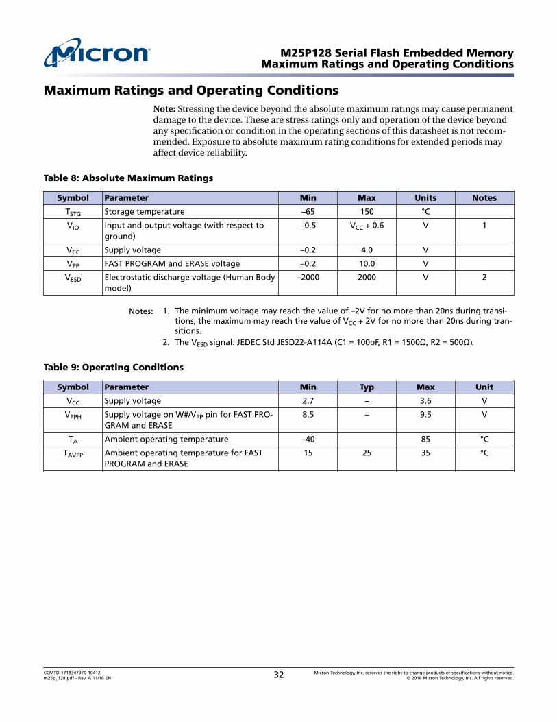
Maximum Ratings and Operating ConditionsNote: Stressing the device beyond the absolute maximum ratings may cause permanentdamage to the device. These are stress ratings only and operation of the device beyondany specification or condition in the operating sections of this datasheet is not recom-mended. Exposure to absolute maximum rating conditions for extended periods mayaffect device reliability.
Table 8: Absolute Maximum Ratings
Symbol Parameter Min Max Units Notes
TSTG Storage temperature –65 150 °C
VIO Input and output voltage (with respect toground)
–0.5 VCC + 0.6 V 1
VCC Supply voltage –0.2 4.0 V
VPP FAST PROGRAM and ERASE voltage –0.2 10.0 V
VESD Electrostatic discharge voltage (Human Bodymodel)
–2000 2000 V 2
Notes: 1. The minimum voltage may reach the value of –2V for no more than 20ns during transi-tions; the maximum may reach the value of VCC + 2V for no more than 20ns during tran-sitions.
2. The VESD signal: JEDEC Std JESD22-A114A (C1 = 100pF, R1 = 1500Ω, R2 = 500Ω).
Table 9: Operating Conditions
Symbol Parameter Min Typ Max Unit
VCC Supply voltage 2.7 – 3.6 V
VPPH Supply voltage on W#/VPP pin for FAST PRO-GRAM and ERASE
8.5 – 9.5 V
TA Ambient operating temperature –40 85 °C
TAVPP Ambient operating temperature for FASTPROGRAM and ERASE
15 25 35 °C
M25P128 Serial Flash Embedded MemoryMaximum Ratings and Operating Conditions
CCMTD-1718347970-10412m25p_128.pdf - Rev. A 11/16 EN 32 Micron Technology, Inc. reserves the right to change products or specifications without notice.
© 2016 Micron Technology, Inc. All rights reserved.
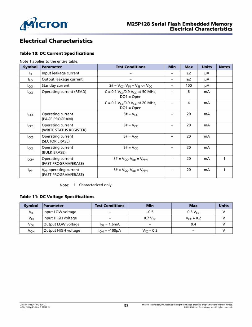
Electrical Characteristics
Table 10: DC Current Specifications
Note 1 applies to the entire table.Symbol Parameter Test Conditions Min Max Units Notes
ILI Input leakage current – – ±2 µA
ILO Output leakage current – – ±2 µA
ICC1 Standby current S# = VCC, VIN = VSS or VCC – 100 µA
ICC3 Operating current (READ) C = 0.1 VCC/0.9 VCC at 50 MHz,DQ1 = Open
– 6 mA
C = 0.1 VCC/0.9 VCC at 20 MHz,DQ1 = Open
– 4 mA
ICC4 Operating current(PAGE PROGRAM)
S# = VCC – 20 mA
ICC5 Operating current(WRITE STATUS REGISTER)
S# = VCC – 20 mA
ICC6 Operating current(SECTOR ERASE)
S# = VCC – 20 mA
ICC7 Operating current(BULK ERASE)
S# = VCC – 20 mA
ICCPP Operating current(FAST PROGRAM/ERASE)
S# = VCC, Vpp = VPPH – 20 mA 1
IPP VPP operating current(FAST PROGRAM/ERASE)
S# = VCC, Vpp = VPPH – 20 mA 1
Note: 1. Characterized only.
Table 11: DC Voltage Specifications
Symbol Parameter Test Conditions Min Max Units
VIL Input LOW voltage – –0.5 0.3 VCC V
VIH Input HIGH voltage – 0.7 VCC VCC + 0.2 V
VOL Output LOW voltage IOL = 1.6mA – 0.4 V
VOH Output HIGH voltage IOH = –100µA VCC – 0.2 – V
M25P128 Serial Flash Embedded MemoryElectrical Characteristics
CCMTD-1718347970-10412m25p_128.pdf - Rev. A 11/16 EN 33 Micron Technology, Inc. reserves the right to change products or specifications without notice.
© 2016 Micron Technology, Inc. All rights reserved.
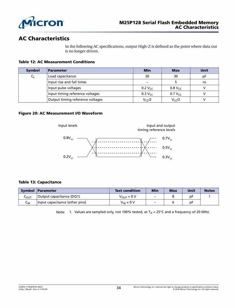
AC CharacteristicsIn the following AC specifications, output High-Z is defined as the point where data outis no longer driven.
Table 12: AC Measurement Conditions
Symbol Parameter Min Max Unit
CL Load capacitance 30 30 pF
Input rise and fall times – 5 ns
Input pulse voltages 0.2 VCC 0.8 VCC V
Input timing reference voltages 0.3 VCC 0.7 VCC V
Output timing reference voltages VCC/2 VCC/2 V
Figure 20: AC Measurement I/O Waveform
Input and outputtiming reference levels
Input levels
0.8VCC
0.2VCC
0.7VCC
0.3VCC
0.5VCC
Table 13: Capacitance
Symbol Parameter Test condition Min Max Unit Notes
COUT Output capacitance (DQ1) VOUT = 0 V – 8 pF 1
CIN Input capacitance (other pins) VIN = 0 V – 6 pF
Note: 1. Values are sampled only, not 100% tested, at TA = 25°C and a frequency of 20 MHz.
M25P128 Serial Flash Embedded MemoryAC Characteristics
CCMTD-1718347970-10412m25p_128.pdf - Rev. A 11/16 EN 34 Micron Technology, Inc. reserves the right to change products or specifications without notice.
© 2016 Micron Technology, Inc. All rights reserved.
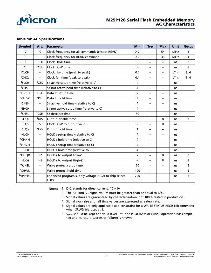
Table 14: AC Specifications
Symbol Alt. Parameter Min Typ Max Unit NotesfC fC Clock frequency for all commands (except READ) D.C. – 54 MHz 1fR – Clock frequency for READ command D.C. – 33 MHz 1
tCH tCLH Clock HIGH time 9 – – ns 2tCL tCLL Clock LOW time 9 – – ns 2
tCLCH – Clock rise time (peak to peak) 0.1 – – V/ns 3, 4tCHCL – Clock fall time (peak to peak) 0.1 – – V/ns 3, 4tSLCH tCSS S# active setup time (relative to C) 4 – – ns tCHSL S# not active hold time (relative to C) 4 – – ns tDVCH tDSU Data In setup time 2 – – ns tCHDX tDH Data In hold time 3 – – ns tCHSH – S# active hold time (relative to C) 4 – – ns tSHCH – S# not active setup time (relative to C) 4 – – ns tSHSL tCSH S# deselect time 50 – – ns tSHQZ tDIS Output disable time – – 8 ns 3tCLQV tV Clock LOW to output valid – – 8 ns tCLQX tHO Output hold time 1 – – ns tHLCH – HOLD# setup time (relative to C) 4 – – ns tCHHH – HOLD# hold time (relative to C) 4 – – ns tHHCH – HOLD# setup time (relative to C) 4 – – ns tCHHL – HOLD# hold time (relative to C) 4 – – ns tHHQX tLZ HOLD# to output Low-Z – – 8 ns 3tHLQZ tHZ HOLD# to output High-Z – – 8 ns 3tWHSL – Write protect setup time 20 – – ns 5tSHWL – Write protect hold time 100 – – ns 5
tVPPHSL – Enhanced program supply voltage HIGH to chip selectLOW
200 – – ns 6
Notes: 1. D.C. stands for direct current. (fC = 0)2. The tCH and tCL signal values must be greater than or equal to 1/fC.3. Signal values are guaranteed by characterization, not 100% tested in production.4. Signal clock rise and fall time values are expressed as a slew rate.5. Signal values are only applicable as a constraint for a WRITE STATUS REGISTER command
when SRWD bit is set at 1.6. VPPH should be kept at a valid level until the PROGRAM or ERASE operation has comple-
ted and its result (success or failure) is known.
M25P128 Serial Flash Embedded MemoryAC Characteristics
CCMTD-1718347970-10412m25p_128.pdf - Rev. A 11/16 EN 35 Micron Technology, Inc. reserves the right to change products or specifications without notice.
© 2016 Micron Technology, Inc. All rights reserved.
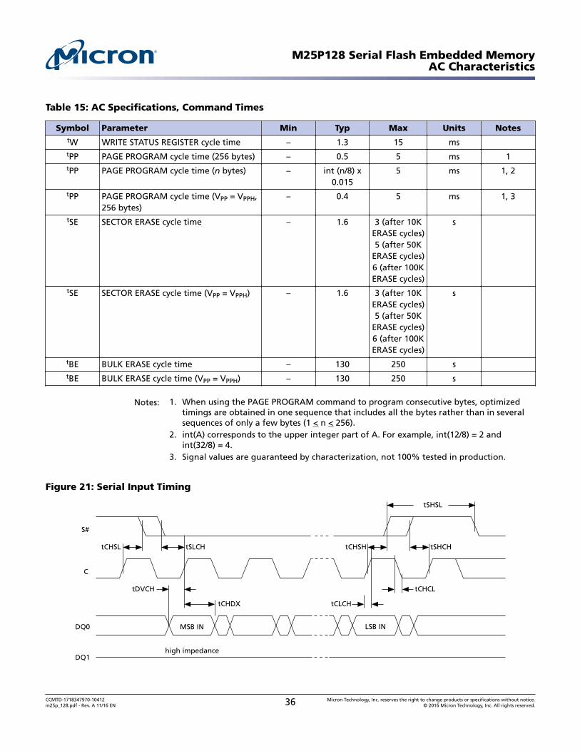
Table 15: AC Specifications, Command Times
Symbol Parameter Min Typ Max Units NotestW WRITE STATUS REGISTER cycle time – 1.3 15 ms tPP PAGE PROGRAM cycle time (256 bytes) – 0.5 5 ms 1tPP PAGE PROGRAM cycle time (n bytes) – int (n/8) x
0.0155 ms 1, 2
tPP PAGE PROGRAM cycle time (VPP = VPPH,256 bytes)
– 0.4 5 ms 1, 3
tSE SECTOR ERASE cycle time – 1.6 3 (after 10KERASE cycles)5 (after 50K
ERASE cycles)6 (after 100KERASE cycles)
s
tSE SECTOR ERASE cycle time (VPP = VPPH) – 1.6 3 (after 10KERASE cycles)5 (after 50K
ERASE cycles)6 (after 100KERASE cycles)
s
tBE BULK ERASE cycle time – 130 250 s tBE BULK ERASE cycle time (VPP = VPPH) – 130 250 s
Notes: 1. When using the PAGE PROGRAM command to program consecutive bytes, optimizedtimings are obtained in one sequence that includes all the bytes rather than in severalsequences of only a few bytes (1 < n < 256).
2. int(A) corresponds to the upper integer part of A. For example, int(12/8) = 2 andint(32/8) = 4.
3. Signal values are guaranteed by characterization, not 100% tested in production.
Figure 21: Serial Input Timing
C
DQ0
S#
MSB IN
DQ1
tDVCH
high impedance
LSB IN
tSLCH
tCHDX
tCHCL
tCLCH
tSHCH
tSHSL
tCHSHtCHSL
M25P128 Serial Flash Embedded MemoryAC Characteristics
CCMTD-1718347970-10412m25p_128.pdf - Rev. A 11/16 EN 36 Micron Technology, Inc. reserves the right to change products or specifications without notice.
© 2016 Micron Technology, Inc. All rights reserved.
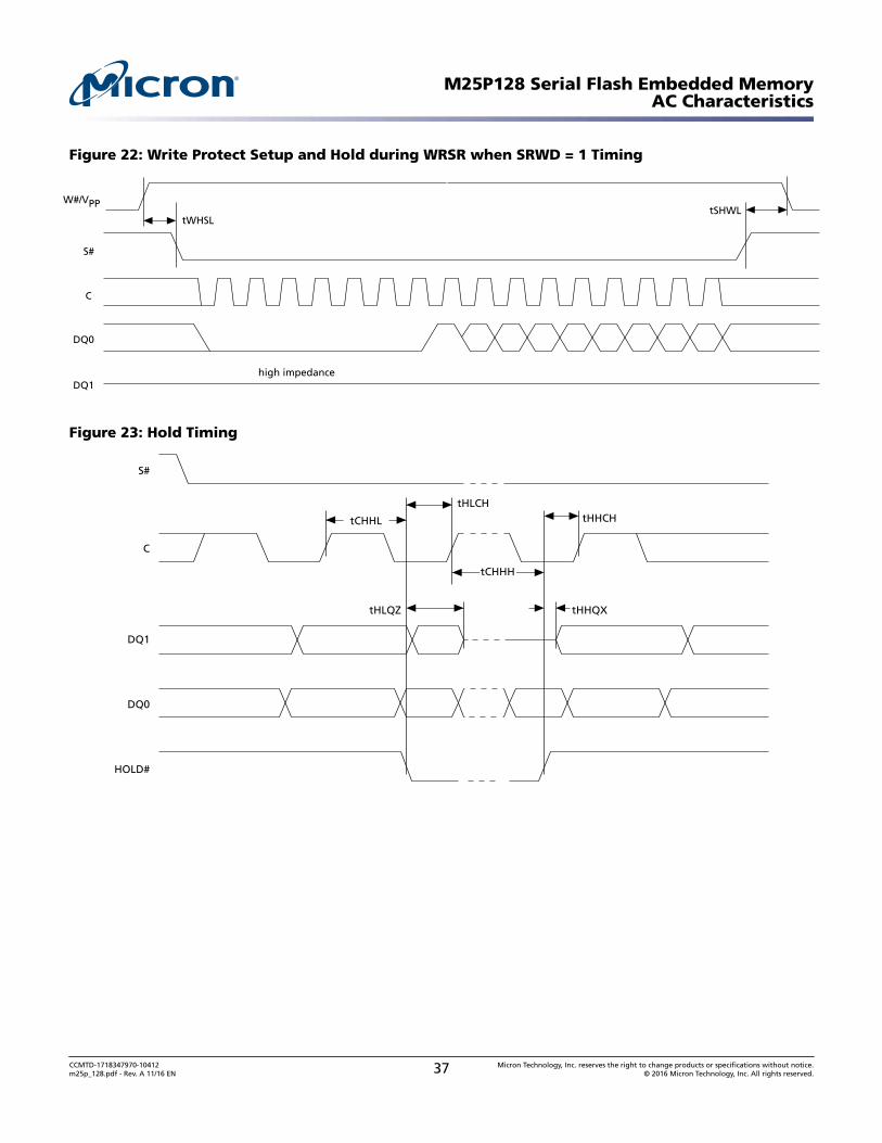
Figure 22: Write Protect Setup and Hold during WRSR when SRWD = 1 Timing
C
DQ0
S#
DQ1high impedance
W#/VPP
tWHSLtSHWL
Figure 23: Hold Timing
tCHHL
tHLCHtHHCH
tHHQXtHLQZ
S#
C
DQ1
DQ0
HOLD#
tCHHH
M25P128 Serial Flash Embedded MemoryAC Characteristics
CCMTD-1718347970-10412m25p_128.pdf - Rev. A 11/16 EN 37 Micron Technology, Inc. reserves the right to change products or specifications without notice.
© 2016 Micron Technology, Inc. All rights reserved.
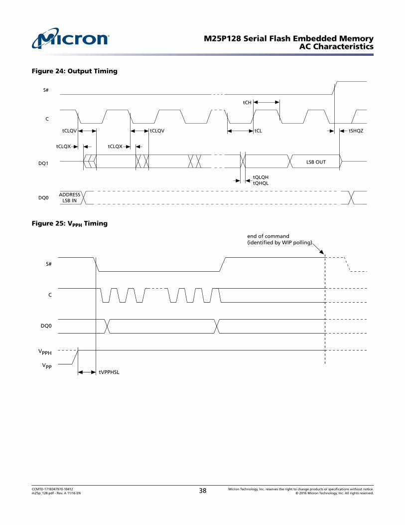
Figure 24: Output Timing
C
DQ1
S#
LSB OUT
DQ0ADDRESS
LSB IN
tSHQZ
tCH
tCL
tQLQHtQHQL
tCLQX
tCLQV
tCLQX
tCLQV
Figure 25: VPPH Timing
S#
C
DQ0
VPP
VPPH
tVPPHSL
end of command(identified by WIP polling)
M25P128 Serial Flash Embedded MemoryAC Characteristics
CCMTD-1718347970-10412m25p_128.pdf - Rev. A 11/16 EN 38 Micron Technology, Inc. reserves the right to change products or specifications without notice.
© 2016 Micron Technology, Inc. All rights reserved.
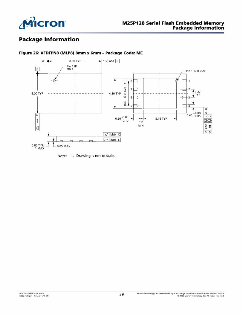
Package Information
Figure 26: VFDFPN8 (MLP8) 8mm x 6mm – Package Code: ME
8.00 TYP
6.00 TYP 4.80 TYP
5.16 TYP0.2MIN
0.50 -0.05+0.10
(NE
- 1)
× 1
.27
TYP
Pin 1 IDØ0.3
1.27TYP
8
7
6
5
1
2
3
4
0.05 MAX
0.40 +0.08-0.05
0.85 TYP/1 MAX
Pin 1 ID R 0.20
ddd C
bbb C
Mee
eC
AB
aaa CA
B
aaa
C
Mff
fC
Note: 1. Drawing is not to scale.
M25P128 Serial Flash Embedded MemoryPackage Information
CCMTD-1718347970-10412m25p_128.pdf - Rev. A 11/16 EN 39 Micron Technology, Inc. reserves the right to change products or specifications without notice.
© 2016 Micron Technology, Inc. All rights reserved.
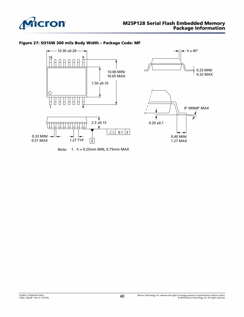
Figure 27: SO16W 300 mils Body Width – Package Code: MF
16
0.23 MIN/0.32 MAX
1 8
9
0.40 MIN/1.27 MAX
0.20 ±0.12.5 ±0.15
10.30 ±0.20
7.50 ±0.10
10.00 MIN/10.65 MAX
0.33 MIN/0.51 MAX
0.1 Z
0° MIN/8° MAX
1.27 TYP
h x 45°
Z
Note: 1. h = 0.25mm MIN, 0.75mm MAX
M25P128 Serial Flash Embedded MemoryPackage Information
CCMTD-1718347970-10412m25p_128.pdf - Rev. A 11/16 EN 40 Micron Technology, Inc. reserves the right to change products or specifications without notice.
© 2016 Micron Technology, Inc. All rights reserved.
Device Ordering Information
Standard Parts
For further information on line items not listed here or on any aspect of this device,contact your nearest representative.
Table 16: Part Number Information Scheme
Part NumberCategory Category Details
Device type M25P = Serial Flash memory for code storage
Density 128 = 128Mb (16Mb x 8)
Operating voltage V = VCC = 2.7V to 3.6V
Package ME = VFDFPN8 8mm x 6mm (MLP8)
MF = SO16W (300 mils width)
Device grade 6 = Industrial temperature range: –40°C to 85°C. Device tested with standard test flow.
Packing option – = Standard packing
T = Tape and reel packing
Plating technology P or G = RoHS-compliant
Lithography B = 65nm SLC
Note: 1. The category of second Level Interconnect is marked on the package and on the innerbox label, in compliance with JEDEC Standard JESD97. The maximum ratings related tosoldering conditions are also marked on the inner box label.
M25P128 Serial Flash Embedded MemoryDevice Ordering Information
CCMTD-1718347970-10412m25p_128.pdf - Rev. A 11/16 EN 41 Micron Technology, Inc. reserves the right to change products or specifications without notice.
© 2016 Micron Technology, Inc. All rights reserved.
Revision History
Rev. A – 11/16
• Initial Micron rebrand.
8000 S. Federal Way, P.O. Box 6, Boise, ID 83707-0006, Tel: 208-368-4000www.micron.com/products/support Sales inquiries: 800-932-4992
Micron and the Micron logo are trademarks of Micron Technology, Inc.All other trademarks are the property of their respective owners.
This data sheet contains minimum and maximum limits specified over the power supply and temperature range set forth herein.Although considered final, these specifications are subject to change, as further product development and data characterization some-
times occur.
M25P128 Serial Flash Embedded MemoryRevision History
CCMTD-1718347970-10412m25p_128.pdf - Rev. A 11/16 EN 42 Micron Technology, Inc. reserves the right to change products or specifications without notice.
© 2016 Micron Technology, Inc. All rights reserved.