Embed Size (px)
Citation preview


Editorial-Chief
Kiyoshi Sakai Editorial Advisors
Toshio Masujima Kotaro Aiba Hiroshi Takenaka Hirotoshi Yonezawa Shinsuke Azuma Chikao Nishida Hitoshi Suzuki Kunihiko Egawa Tetsuyuki Yanase Tadashi Kato Hiroaki Imamura Shinji Yamana Takafumi Kawai Masato Oshita Toshihiro Kurita
Vol. 153 Feature Articles Editor
Kazuya Yamamoto Editorial Inquiries
Kiyoshi Sakai Corporate Total Productivity Management & Environmental Programs Fax: +81-3-3218-2465
Product Inquiries
NORTH AMERICA Mitsubishi Electric US, INC. Semiconductor Division 5900-A Katella Avenue, PO BOX 6007, Cypress, CA 90630-5019, U.S.A. Danyo Tu E-mail:[email protected]. com GERMANY Mitsubishi Electric Europe B.V. German Branch Semiconductor - European Business Group Mitsubishi-Electric-Platz 1, 40882 Ratingen, Germany Corinna Meyer Fax: +49-(0)2102-486 4140 CHINA Mitsubishi Electric & Electronics (Shanghai) Co., Ltd 29 Floor, Shanghai MAXDO Center No. 8, Xing Yi Road, Hong Qiao, Shanghai 200336, China Qian Yu Feng Fax: +86-21-5208-1502 Mitsubishi Electric Advance is published on line quarterly (in March, June, September, and December) by Mitsubishi Electric Corporation. Copyright © 2016 by Mitsubishi Electric Corporation; all rights reserved. Printed in Japan.
The company names and product names described herein are the trademarks or registered trademarks of the respective companies.
CONTENTS
Technical Reports
Overview .......................................................................................... 1 by Yoshihito Hirano 25.8 Gbps Direct Modulation DFB Lasers of 4 Wavelengths for 100 Gbps Transmission ................................................................ 2 by Go Sakaino and Naoki Nakamura A Laser Module for 100Gbps Digital Coherent Optical Transmission System ..................................................................... 5 by Keita Mochizuki and Mitsunobu Gotoda Low Power Consumption 25Gbps EML-TOSA for CFP Optical Transceiver ...................................................................................... 8 by Mikio Baba and Takeshi Yamatoya 638-nm High Power Red Laser Diode for Projectors ................ 10 by Kyosuke Kuramoto High Power Ku-band GaN MMIC and Internally Matched HEMTs for Satellite Communication .............................................................. 12 by Tetsuo Kunii and Koh Kanaya GaAs HEMTs for Low Noise Amplifier in Automotive Application .......................................................................................................... 16 by Toshikazu Hirayama
Mitsubishi Electric
Mar. 2016 / Vol. 153
Recent Advances in Optical and Microwave Devices
Precis
The increasing demand for greater convenience has driven the development of high-speed, high-power, and highly reliable optical and microwave devices.
This article introduces new optical and microwave devices developed by Mitsubishi Electric for use in optical fiber links, projectors, satellite communications, and automobile applications.

*Group Vice President, High Frequency & Optical Device Works Mitsubishi Electric ADVANCE March 2016 1
TECHNICAL REPORTS
Overview
Author: Yoshihito Hirano*
Status and Outlook of High Frequency & Optical Devices
Both wireless and wired communication networks have become indispensable to modern society. Since 2000, network services such as internet browsing, video streaming, and the growing online shopping business have produced a huge data transmission on communication networks at an explosive pace. To support this traffic, there is a strong demand for compact high-frequency and optical devices that consume less power.
Wireless communication systems that use high-frequency devices, such as wireless LANs (local area networks), cellular phones, and satellite communications, have come into wide use in recent years. For mobile and satellite communication base stations, GaN (gallium nitride) devices make their way into high-power amplifiers with high output and compact features due to their high-voltage operation.
Regarding wired communication systems that use optical fiber to connect countries around the world, there is strong demand for optical devices capable of high-speed operation of 25 Gbps (gigabits per second) and 100 Gbps with a compact size and less power consumption simultaneously to support the ever-increasing traffic.
This feature article looks at the current status of these high-frequency devices and optical devices, also focuses on next-generation devices that support wireless and wired communication infrastructures.
*High Frequency & Optical Works 2
TECHNICAL REPORTS
25.8 Gbps Direct Modulation DFB Lasers of 4 Wavelengths for 100 Gbps Transmission
Authors: Go Sakaino* and Naoki Nakamura*
1. Introduction
Inside a data center where a large volume of data communication is concentrated, high-speed transmission at 100 Gbps is essential. As the densely packed optical transceivers consume much electricity, there is a demand for reduced power consumption. The direct modulation distributed feedback laser diode (DFB-LD), which can operate at high temperature and low current, is a promising optical source for transceivers that satisfies this demand. Accordingly, we developed a 4-wavelength 25.8 Gbps direct modulation DFB-LD, which can operate at 75°C and a low current.
2. Device Design
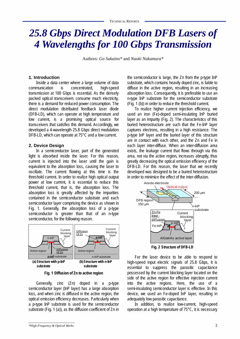
In a semiconductor laser, part of the generated light is absorbed inside the laser. For this reason, current is injected into the laser until the gain is equivalent to the absorption loss, causing the laser to oscillate. The current flowing at this time is the threshold current. In order to realize high optical output power at low current, it is essential to reduce this threshold current, that is, the absorption loss. The absorption loss is greatly affected by the impurities contained in the semiconductor substrate and each semiconductor layer comprising the device as shown in Fig. 1. Generally, the absorption loss of a p-type semiconductor is greater than that of an n-type semiconductor, for the following reason.
(a) Structure with p-InP
substrate (b) Structure with n-InP
substrate
Fig. 1 Diffusion of Zn to active region Generally, zinc (Zn) doped in a p-type
semiconductor layer (InP layer) has a large absorption loss, and when zinc is diffused in the active region, the optical emission efficiency decreases. Particularly when a p-type InP substrate is used for the semiconductor substrate (Fig. 1 (a)), as the diffusion coefficient of Zn in
the semiconductor is large, the Zn from the p-type InP substrate, which contains heavily doped zinc, is liable to diffuse in the active region, resulting in an increasing absorption loss. Consequently, it is preferable to use an n-type InP substrate for the semiconductor substrate (Fig. 1 (b)) in order to reduce the threshold current.
To realize higher current injection efficiency, we used an iron (Fe)-doped semi-insulating InP buried layer as an impurity (Fig. 2). The characteristics of this buried heterostructure are such that the Fe-InP layer captures electrons, resulting in a high resistance. The p-type InP layer and the buried layer of this structure are in contact with each other, and the Zn and Fe in each layer inter-diffuse. When an inter-diffusion area exists, the leakage current that flows through via this area, not via the active region, increases abruptly, thus greatly decreasing the optical emission efficiency of the DFB-LD. For this reason, the laser that we recently developed was designed to be a buried heterostructure in order to minimize the effect of the inter-diffusion.
Fig. 2 Structure of DFB-LD
For the laser device to be able to respond to
high-speed input electric signals of 25.8 Gbps, it is essential to suppress the parasitic capacitance possessed by the current blocking layer located on the side of the active region for effective injection current into the active regions. Here, the use of a semi-insulating semiconductor layer is effective. In this device, we used an Fe-doped InP layer, resulting in adequately low parasitic capacitance.
In addition, to realize low-current, high-speed operation at a high temperature of 75°C, it is necessary
Active region
n-InP
p-InP substrate
DiffusionOf Zn
Current
Active region
p-InP
n-InP substrate
DiffusionOf Zn
blockinglayer
Currentblocking
layer
Fe-InPp-InP
Currentblocking
Zn-FeInter-dif fusion
AlGaInAs active layer
layer
n-InPsubstrate
200 μm
Optical outputAnode electrode
150 μmDFB region

Mitsubishi Electric ADVANCE March 2016 3
TECHNICAL REPORTS
to suppress the deterioration of the optical modulation waveform due to the optical oscillation, which is a particular characteristic of lasers as a result of the interaction between electricity and light. The frequency of this optical oscillation is called the relaxation oscillation frequency (fr). To obtain a clear optical modulation waveform, it is important to maintain the high-temperature fr at a high value roughly equal to the modulation signal frequency. Accordingly, it is necessary to minimize the optical loss, which is prominent at high temperature, minimize the efficiency reduction of current injection to the active region, and minimize the reduction of light density in the active region and the attendant reduction of fr. Consequently, in order to realize high-speed operation, we approached the design from the viewpoint of achieving a high relaxation oscillation frequency, in addition to using a low parasitic capacitance buried layer.
As shown in the equation below, fr is proportional to the square root of the difference between the operating current (Iop) and the threshold current (Ith). To maintain the necessary fr when performing low-current operation, it is useful to reduce the threshold current.
fr [(Iop-Ith)/p]1/2 p: Photon lifetime To realize the above, the use of an n-type
semiconductor substrate, which is effective for realizing low optical loss, is helpful as mentioned previously. Also, in order to achieve a high fr, it is generally useful to increase the differential gain as the ratio of the gain with respect to the current injection. Consequently, a high differential gain can be realized by using an AlGaInAs active region that the leakage of electrons at high temperature is suppressed, because the depth of the multi-quantum well relative to the electrons in the conduction band is large. Likewise, to achieve a high fr, it is also useful to shorten the photon lifetime as well as reduce the length of the cavity. In this development, the cavity length is 150 m in consideration of the fact that adequate gain can also be obtained over the operating temperature range of −5°C to +75°C, and also the amount of detuning, which corresponds to the difference between the peak wavelength of the gain spectrum and the DFB oscillation wavelength, is set to a suitable value, to increase the differential gain.
Note that data communication at 100 Gbps uses a 4-wavelength direct modulation DFB-LD that operates at 25.8 Gbps, and is realized by a wavelength multiplexing for combining each optical signal. According to the CWDM (Coarse Wavelength Division Multiplexing) standard in which the interval between each of the four wavelengths is specified to be 20 nm
and the allowable width of each waveform is specified to be 13 nm, uncooled operation is possible. For this reason, the effectiveness of this method is recognized, and CWDM4 and CLR4 have been established as multi-source agreements (MSA) for practical application. We designed a 4-wavelength direct modulation DFB-LD that can be applied to these MSAs.
Based on the abovementioned design, we fabricated a 4-wavelength direct modulation DFB-LD with the construction shown in Figs. 2 and 3. After an n-type InP substrate was used to form a grating, the AlGaInAs active region was grown. In addition to a p-type and an n-type InP layer, we installed a high-resistance low parasitic capacitance current blocking layer that used the abovementioned Fe-doped InP layer, on the side face of the active region. To suppress the effect of the inter-diffusion of Fe and Zn, the current blocking layer is fabricated to a shape that minimizes the area of contact between the p-InP clad layer and the Fe-InP layer at the top of the active region. The cavity length is made extremely short at 150 m. Also, to facilitate handling of the laser during the assembly process, the optical waveguides are integrated at the optical output side, and the total length of the device in the cavity direction is made 200 m.
Fig. 3 Longitudinal structure of DFB-LD
3. Device Characteristics
Figure 4 shows the current versus optical output characteristics of the DFB-LD for each of the four wavelengths. Regardless of the wavelength of the device, when the maximum temperature is 75°C, the threshold current is no more than 13 mA, and the slope efficiency is at least 0.2 mW/mA. In other words, low threshold current and high efficiency are realized simultaneously, and a high output of at least 10 mW is acquired as the maximum optical output as well.
As it is necessary to miniaturize a transceiver in 100 Gbps optical communication that simultaneously uses 25.8 Gbps-modulation 4-wavelength DFB-LDs, the four DFB-LDs are mounted as a single package. Compared to the case where an optical signal is transmitted as a single wavelength, the optical loss of the structure with four DFB-LDs increases due to multiplexing the wavelengths. Regarding the newly developed 4-wavelength DFB-LD, a high output is achieved for all four wavelengths, demonstrating that the design limitations on the optical multiplexing construction can be reduced by compensating for this
Optical output
n-InP
p-InP
Waveguide(InGaAsP) 50 µm 150 µm
Gratings
Antireflective coat High reflective coat
AlGaInAsactive layer

4
TECHNICAL REPORTS
optical loss. It is considered that such a high output is the result of using an n-type InP substrate with a small absorption loss, as described previously, and also using the Fe-doped InP layer of a structure that allows high current injection efficiency to be achieved while suppressing mutual diffusion of Fe and Zn, as a current blocking layer. As a large relaxation oscillation frequency (fr) has been obtained owing to these satisfactory optical output characteristics even at a high temperature of 75°C, the current dependence of fr is obtained. These values indicate that the higher the current dependence, the greater the fr is that can be obtained at a low consumed current, thus allowing the device to operate with small current consumption. The values for the current efficiency of fr obtained during this development were 3.9, 3.6 and 3.0 GHz/(mA)1/2 at −5°C, 25°C and 75°C, respectively, which are large values, indicating that high-speed modulation is possible even at high temperature.
Based on these large fr values realized together with a low threshold current and high output at 75°C, a clear optical waveform in a 25.8 Gbps has been obtained, which is important for optical transmission. Figure 5 shows the modulated waveforms.
−5C 25C 75C
Ib: average bias current, MM: Mask margin (Extinction ratio: 5dB)
Fig. 5 25.78125 Gbps eye diagram
4. Summary The developed device realizes low power
consumption, low cost, and miniaturization of optical transceivers, and is expected to contribute to the expansion of 100 Gbps short-distance optical communication.
Fig. 4 I-L characteristics (−5, 25, 75°C)
0
2
4
6
8
10
12
14
16
0 10 20 30 40 50 60 70 80
Out
put p
ower
(m
W)
Current (mA)
0
2
4
6
8
10
12
14
16
0 10 20 30 40 50 60 70 80O
utpu
t pow
er (
mW
)Current (mA)
1290 nm
25oC-5oC
75oC
1270 nm
25oC-5oC
75oC
0
2
4
6
8
10
12
14
16
0 10 20 30 40 50 60 70 80
Out
put p
ower
(m
W)
Current (mA)
0
2
4
6
8
10
12
14
16
0 10 20 30 40 50 60 70 80
Out
put p
ower
(m
W)
Current (mA)
1330 nm
25oC
75oC
1310 nm
25oC
75oC
-5oC-5oC

*Information Technology R & D Center **Advanced Technology R&D Center Mitsubishi Electric ADVANCE March 2016 5
TECHNICAL REPORTS
A Laser Module for 100Gbps Digital Coherent Optical Transmission System
Authors: Keita Mochizuki* and Mitsunobu Gotoda**
We recently developed a 100 Gbps digital coherent transmission laser module. As the key to realizing miniaturization, low power consumption and high output, we established a wavelength tunable LD (laser diode) device that has an array of 16 LDs, and also wavelength monitoring technology using the light emitted from the back of the LD, and successfully obtained the characteristics required for transmission.
1. Introduction
The 100 Gbps digital coherent system uses a wavelength tunable laser device that enables the wavelength of the emitted light to be varied, as the light source for the transmitter and also as the local oscillator light source for the receiver. The interface is standardized as an ITLA (integrable tunable laser assembly) by the OIF (Optical Internetworking Forum). In this paper, we report on the development of a laser module that complies with the standard for the Micro-ITLA,(1) which is one size smaller than the ITLA. This standard was ratified aiming at second-generation optical transceivers.
2. Structure of the Laser Module
Figure 1 is a photograph of the 100 Gbps digital coherent transmission laser module that we developed. The external size of the module excluding the fiber is 45207.5 (mm), which complies with the Micro-ITLA standard. Figure 2 shows the internal structure of the package. The package consists of a wavelength tunable LD, a TEC (thermo-electric cooler) which regulates the wavelength tunable LD temperature, an optical power monitor that detects the power of the emitted light, and a wavelength monitor that detects the wavelength of the emitted light. The wavelength tuning
method is a temperature regulating type that uses a highly stable DFB (distributed feedback) LD. The light emitted from the front side (output side of the laser module) of the wavelength tunable LD passes through a lens where it is coupled to the optical fiber. The light emitted at the rear side (opposite side) enters the rear-side wavelength monitor. Based on the information detected by the monitor, the injection current and the temperature of the wavelength tunable LD are controlled by a control circuit, thus stabilizing the optical output and wavelength.
Generally, in order to realize the various characteristics required for 100 Gbps digital coherent transmission, namely an optical output of at least 14.0 dBm, power consumption of no more than 5.0 W, linewidth of the output of no more than 500 kHz, and optical frequency stability of 2.5 GHz, it is necessary to resolve two major issues. The first one is the question of how to simultaneously reduce the power consumption and realize high optical output. In order to cover the entire wavelength bands (C, L bands) used for optical communication, it is necessary to vary the temperature of the DFB LD section over a wide range, and also integrate multiple DFB LDs that emit light of different wavelengths. However, widening of the temperature adjustment range causes the TEC power consumption to rise, while an increase in the number of DFB LDs results in a greater loss in the coupler section where the light emitted from each LD is combined. The second issue is the realization of a highly accurate rear-side wavelength monitor. A wavelength monitor consists of an etalon,
Fig. 1 Photograph of the developed laser module for the digital coherent transmission
Fig. 2 Construction of the developed laser module for the digital coherent transmission

6
TECHNICAL REPORTS
which is an optical filter, and a PD (photodiode), which receives light that has passed through the etalon. As the transmittance of an etalon depends upon the wavelength, any fluctuation in the wavelength of the emitted light can be detected as a fluctuation of the optical power received by the PD. In this development, in order to save the power consumption, we developed a wavelength monitor structure that uses the light emitted from the rear side of the wavelength tunable LD, which is not normally used. However, in the case of a wavelength tunable LD comprising integrated multiple DFB LDs, the characteristics of the wavelength monitor for each DFB LD vary from one monitor to the other, making it difficult to realize a highly accurate wavelength monitor. The technology used in this model to resolve both of these issues is described below.
3. Technology Used in a Laser Module
3.1. Wavelength tunable LD
Figure 3 is a schematic diagram showing the construction of the newly developed wavelength tunable LD.(2) This LD consists of an array of 16 DFB LDs integrated on an InP (indium phosphide) substrate, S-bent passive waveguides, an MMI (multimode interference) optical coupler, an SOA (semiconductor optical amplifier), and unequally spaced passive waveguides for the rear-side wavelength monitor. The chip size is 4.80.50.1 (mm). The light emitted from the DFB LDs passes through the S-bent passive waveguides and the 161 MMI optical coupler, and is then amplified by the SOA. The pitch of the grating of each DFB LD is designed so that all 88 channels in the L band (1565-1625 nm, 50 GHz spacing ITU-T grid) can
be covered when the temperature adjustment range of the wavelength tunable LD is 30°C or less. Also, in order to simultaneously realize a linewidth of no more than 500 kHz and high optical output, we used a long DFB LD cavity that has a length of 1.2 mm, and also optimally designed the shape of the waveguide of the SOA. Figure 4 shows the dependency of the output power of the optical fiber to which the light emitted from the front side is connected on the SOA current. Measurement was carried out when the temperature of the wavelength tunable LD was 25°C and 55°C, and in addition the current injected into all 16 DFB LDs was a constant 180 mA. At both temperatures, optical fiber output of at least 14 dBm was obtained.
3.2 Rear-side wavelength monitor
Figure 5 shows the construction of the conventional front-side wavelength monitor and the newly developed rear-side wavelength monitor. The newly developed structure minimizes the branch loss of the light emitted from the front side of the wavelength tunable LD. However, the wavelength monitor characteristics vary randomly for each driving DFB LD. This is caused by variations in the angle of incidence of the light to the etalon, which in turn is due to the different locations of rear-side emission points for each DFB LD. We utilized the fact that the transmittance of the etalon has a periodic spectrum, and carried out the design to modify the location of each rear-side emission point of DFB LD as unequal so that the transmittances coincide on equal frequency grids for all of driving DFB LDs.(3) Figure 6 shows the wavelength monitor characteristics of the prototype laser module. Due to the etalon angle of incidence that differs from one beam
Fig. 6 Measured etalon spectral transmittances of the lights from the unequally spaced 16 emitting-point array
Fig. 4 Measured fiber output power of 16-DFB LD by changing the SOA current
Fig. 3 Schematic structure of the developed wavelength tunable LD
Fig. 5 Construction of a wavelength monitor
(a) Conventional front-side type (b) Proposed rear-side type
Output Lens
Wavelength tunable LD Etalon
PDLens
MMI
SOA
DFB LD array
Output
LensWavelength tunable LD
SOA
MMI
DFB LD arrayEtalon
PD

Mitsubishi Electric ADVANCE March 2016 7
TECHNICAL REPORTS
to another, the spectra of the light emitted from the DFB LD do not match each other; however, the wavelength monitor coefficients in the ITU-T grid, match each other. At that time, the random variations in the wavelength monitor characteristics were within 1.2 GHz, which is within the target value of 2.5 GHz.
4. Characteristics of Laser Module
We evaluated the characteristics of the newly developed 100 Gbps digital coherent transmission laser module. Figure 7 shows the optical output for each wavelength channel, Fig. 8 shows the power consumption, Fig. 9 shows the linewidth of the emitted light, and Fig. 10 shows the stability of the light frequencies. The tunable range of the wavelength is the entire L band, which consists of a total of 88 channels.
Fig. 7 Measured fiber output powers
Fig. 8 Measured power consumptions
Fig. 9 Measured linewidth of the output light
Fig. 10 Measured deviation of locking frequencies from
ITU-T grid points
The measured characteristics of the optical module are indicated below. All of these results satisfy the target values.
The optical output for all channels is 14.3 dBm or higher. The power consumption is 3.6 W or less when the case temperature is 75°C, which is the worst condition. The linewidth of the emitted light beam is 320 kHz or less. This measurement is limited to the worst condition for each LD. The discrepancy of the emitted light frequency from the ITU-T grid is 0.6 GHz or less.
5. Summary
We have developed a 100 Gbps digital coherent transmission. This laser module is expected to serve as a key device for the miniaturization of 100 Gbps digital coherent transmission systems while also reducing power consumption, thus paving the way for various applications in the future.
References (1) OIF-MicroITLA-01.0 (2011)
http://www.oiforum.com/public/documents/OIF- microITLA-01.0.pdf (2) Horiguchi, Y., et al., The 24th ISLC, TC2 (2014) (3) Mochizuki, K., et al., The 24th ISLC, TC3 (2014)

*High Frequency & Optical Device Works 8
TECHNICAL REPORTS
Fig. 1 25 Gbps EML-TOSA and CFP Optical Transceiver in optical network
Low Power Consumption 25Gbps EML-TOSA for CFP Optical Transceiver
Authors: Mikio Baba* and Takeshi Yamatoya*
1. Introduction
Along with the increase in number of communication terminals, diversification of information storage devices/processing methods and increasing density of information, the volume of communication in each layer of communication networks such as core/metro/access is also increasing. As a result, the increase in communication speed involved in the integration of information, and the reduction of growing power consumption due to the increase in number of communication equipments, are significant issues. International standards established by such organizations as IEEE (Institute of Electrical and Electronics Engineers) and ITU-T (International Telecommunication Union Telecommunication Standardization Sector) have standardized a 100 Gbps optical interface that multiplexes four different optical wavelengths at a bit rate of 25 Gbps. Also, under the CFP-MSA (Centum Gigabit Form-Factor Pluggable Multi-Source Agreement),(1) optical transceivers for metro networks have been proposed.
This paper presents the 25 Gbps EML-TOSA (electro-absorption modulator-integrated laser – transmitter optical subassembly) (Fig. 1), which was developed for use in a 100 Gbps optical network.
2. Improvement of Package
Taking into consideration the standardization of
parts and their manufacturing method, as well as the handling method on the customer’s side, the external appearance and terminal arrangement used in this TOSA comply with the interface standard for the 10 Gbps XMD MSA (10 Gbps Miniature Device Multi-Source Agreement),(2) which has a proven record for current 10 Gbps transceivers. Furthermore, the flexible printed circuit and package were improved. As a result, the newly developed package has improved frequency characteristics compared to those of the XMD MSA.
3. New EML Chip
Figure 2 shows the construction of the newly developed hybrid waveguide type EML device (top view).(3) In contrast to the construction of the current devices, the LD (laser diode) section was made as an embedded type with excellent high-temperature characteristics, allowing an increase in the set temperature from 40C to 55C for temperature control, aiming at realizing a power-saving thermoelectric cooler. Also, the EAM (electro-absorption modulator) section was made longer and narrower in order to permit high-speed operation even when the modulation voltage is small; it is also a high-mesa type that maintains the high optical confinement factor even with the narrowed width.(4)
By thus using different waveguide constructions for the LD and EAM sections, each section can be

Mitsubishi Electric ADVANCE March 2016 9
TECHNICAL REPORTS
optimized, realizing excellent characteristics overall. In addition, the spot-size converters are integrated at the front end of the device, resulting in a construction that facilitates alignment assembly of the optical axis.
Fig. 2 Hybrid waveguide 25 Gbps EML chip structure
4. Results
Taking into consideration actual use by the customer, we evaluated the connection with the commercially available KGL8105(5) driver IC manufactured by NeoPhotonics, and the low power consumption MAOM-002204(6) driver IC manufactured by MACOM. Table 1 and Fig. 3 show the evaluation results. For reference, Table 1 also shows the results for a TOSA on which a current EML device is mounted.
The newly developed TOSA consumes 0.15 W even when the case temperature is 80C, achieves an adequate extinction ratio even when the modulation voltage is as small as 1.5 V.
In the case of a CFP optical transceiver, EML-TOSAs and driver ICs for four wavelengths are necessary. Comparing the power consumption when using the existing EML-TOSAs and ordinary driver ICs with that when using the newly developed integrated TOSA and low power consumption driver IC, the former would be 4 (1.25 + 0.43) = 6.72 W, and the latter would be 4 (0.75 + 0.15) = 3.6 W. In other words, the power consumption will be reduced by 3.12 W per CFP optical transceiver.
In addition, along with the reduced power consumption, the device can also be used with the next-generation CFP2 optical transceiver, which is one-third the volume of the existing CFP optical transceiver.
5. Conclusion
We developed a 25 Gbps EML-TOSA on which an EML device that utilizes a hybrid waveguide is mounted. This 25 Gbps EML-TOSA satisfies the international standard (8 dB) concerning the extinction ratio, even when the modulation voltage is low. Also, in LD high temperature operation, the power consumption per CFP optical transceiver is reduced by about 3 W.
This newly developed EML-TOSA realizes 100 Gbps rate and low power that resolves the issues of increasing volume of information communication and increase in power consumption, and will contribute the
progress of optical communication systems and environmental protection.
Table 1 Evaluation results
No. Item Current TOSA
Hybrid waveguide chip TOSA
KGL8105 KGL8105 MAOM-002204
1 LD temperature (C)
40 55 55
2 LD current (mA) 60 91 85 3 Modulation
voltage (V) 2.0 2.0 1.5
4 Optical output (dBm)
2.0 1.7 1.32
5 Extinction ratio (dB)
8.8 10.8 9.05
6 Mask margin (%) 42 31 34
7 Power consumption (W)(Tc = 80C)
0.43 0.15 0.15
(a) Driven by KGL8105A
(b) Driven by MAOM-002204
Fig. 3 Optical Waveforms
References (1) CFP-MSA: http://www.cfp-msa.org (2) XMD-MSA: http://www.xmdmsa.org/ (3) Takeshi Yamatoya, et al.: Low-Voltage and
High-Temperature Operation of 28 Gb/s EMLs with Hybrid Waveguide Structure for Next-Generation 100GbE Transceivers, The Institute of Electronics, Information and Communication Engineers (2013), C-4-18
(4) Fukano, et al., IEICE technical report, vol. 104, No. 414, LQE2004-100, pp. 47-50.(2004)
(5) NeoPhotonics: http://www.neophotonics.com/ (6) M/A-COM: http://www.macom.com/home.html
Buried LDHigh Mesa
EAMSpot size converter

*High Frequency & Optical Device Works 10
TECHNICAL REPORTS
638-nm High Power Red Laser Diode for Projectors
Author: Kyosuke Kuramoto*
In order to improve the brightness, efficiency, and reliability of projectors, it is desirable to use laser diodes (LDs) as the light source. Recently, Mitsubishi Electric announced mass production of a red LD that can emit the world’s highest output of 2.5 W under pulse condition with wavelength of 638 nm.1 The LD is equipped with our original high-output technologies and assembled on a 9 mm diameter TO CAN, offering brilliant and deep red color.
1. Introduction
While high-pressure mercury lamps have been widely used as light sources for projectors so far, LDs have advantages such as higher efficiency, wider color gamut, highly-reliable operation, low environment impact, and so on. Projectors with blue LDs and phosphors have already started to penetrate into the market.
Red LDs, on the other hand, have not been used for the light source because of insufficient optical output per device. There are two causes to prevent the red LD from high power operation. One is the catastrophic optical degradation (COD) due to light absorption at the front facet of the LD. Another is the light output saturation due to the temperature rise in the active layer.
An effective method of preventing COD is to reduce the light density at the facet of the laser diode. In this LD, the total width of the light emitting region was increased from the previous value of 40 μm to 180 μm. The emitting region was divided into three regions, each with a width of 60 μm. Dividing the emitting region reduces the heat generation density, allowing for the active layer temperature to be kept low.
Figure 1 shows the schematic structure of the LD. The LD equipped with our original window-mirror structure for an additional measure against COD. Zinc was selectively introduced into the facet mirror region as an impurity and disordering the active laser was performed by annealing.
In addition, in order to lower the active layer temperature, the newly developed 9 mm TO-CAN was used for the package, contrary to the previous LD that is assembled on 5.6 mm open TO. The large 9 mm TO reduces both the thermal resistance of the package and the thermal contact resistance between the 1 As of November 5, 2015
package and the LD holder.
2. Device Characteristics The light output power versus injection current
characteristics of the previous and this product are shown in Fig. 2 (a) and (b), respectively. The drive condition was pulse operation with a duty cycle of 30% and frequency of 120 Hz; the temperature indicated in the figure was the temperature at the bottom surface of the package (case temperature).
The previous product showed the output power saturation at the high temperature and/or high output power regions. On the other hand, the newly developed are showed excellent characteristics exceeding 2.5 W at the case temperature between 25 and 45°C.
Operation current at output power of 2.5 W, case temperature of 25°C and 45°C were 2.71 A and 3.41 A, respectively. The corresponding operation voltages were 2.26 V and 2.33 V, respectively. The slope efficiency at 25°C was 1.20 W/A.
The beam divergence angles along the slow and fast axes with the peak power of 2.54 W at the case temperature of 25°C were 7.3° and 73.6°, respectively. The values were the angles at the position where the light intensity was 1/e2 of the maximum value.
The peak wavelength was 638.6 nm, and the full width at half maximum of the spectrum was approximately 1.6 nm.
3. Reliability
Figure 3 shows the aging test results of the product. The aging condition was auto current control mode with the initial power of 3.4 W under the CW operating condition. The case temperature was set to be equivalent to that at the ambient temperature of 25°C
Fig. 1 Device structure of the red LD

Mitsubishi Electric ADVANCE March 2016 11
TECHNICAL REPORTS
during pulse operation with the duty of 30%. Considering that the degradation rate due to COD is proportional to the power of 3.2 of the optical output power, the acceleration factor of this aging test was 2.68 (=[3.4 W/2.5 W] 3.2). Based on this factor, the aging duration of 5,500 hours at 3.4 W is equal to
49,000 hours at 2.5 W with the duty of 30%, indicating that this LD has high reliability.
4. Summary
The high power red LD for the light source of the projector was newly developed and launched. The LD has the maximum power rating of 2.5 W under the pulse operation, which is the world’s highest output record for a CAN package type red LD in the 638 nm band to the best of our knowledge.
Mitsubishi Electric is developing the LDs with even higher power for pulse operation and also the LDs for CW operation to meet the demand for high-brightness projectors.
(a) Developed product
(b) Developed product
Fig. 2 Output power – current characteristics
Fig. 3 Aging test result

*High Frequency & Optical Device Works 12
TECHNICAL REPORTS
High Power Ku-band GaN MMIC and Internally Matched HEMTs for
Satellite Communication Authors: Tetsuo Kunii* and Koh Kanaya*
1. Introduction
In the satellite communication market, both the increase in communication traffic and the growth in demand for mobile stations are advancing, and there is a strong demand for higher output power, more compact transmitters for satellite communication earth stations. By using GaN (gallium nitride) with high dielectric breakdown voltage instead of the conventional GaAs, we realized high-voltage operation and high power density, and developed a miniature, high output power device for a transmitter. With the newly developed device, a lineup of Ku-band devices consisting of two types of internally matched GaN high electron mobility transistors (HEMTs) and GaN monolithic microwave integrated circuits (MMIC) for driver-stage has been commercialized (Fig. 1).
Fig. 1 Ku-band GaN MMIC and GaN HEMTs
2. 50 W Internally Matched HEMT
In order to realize high gain in the high-frequency Ku band (between 13.75 and 14.5 GHz in the case of an earth station), we developed a GaN transistor with a gate length (Lg = 0.25 m) that is shorter than the gate length (Lg = 0.75 m) of the C-band transistor already being mass-produced.(1) The frequency (fk), which indicates the point of conversion between the maximum stable gain (MSG) and the maximum available power gain (MAG) of the developed transistor (Wg = 50 m 10), was increased from the previous 13.8 GHz to 19.5 GHz, which is an improvement of approximately 1.5-fold. As a result, it was found that this product has adequate high-frequency performance as a Ku-band transistor.
Figure 2 shows the evaluation results for the input power versus output power characteristics of the Ku-band 50 W internally matched HEMT (MGFK47G3745A), which uses this transistor. A saturated output power of 47 dBm (50 W), linear gain of 8.0 dB, and power-added efficiency (PAE) of 30% are obtained at 14.125 GHz. The package size of this
product is 21.012.94.5 (mm), and an output of 50 W has been realized simultaneously with downsizing to an even smaller package than that of the conventional 25 W GaAs FET.
Fig. 2 RF Characteristics of Ku-band 50W HEMT
(MGFK47G3745A) Figure 3 shows the third-order intermodulation
distortion (IM3) characteristics of this device. The output power at IM3 = −25 dBc (linear output power) that is required to secure the necessary communication quality for a satellite communication earth station is 45 dBm at the power supply voltage of 24 V. The device has the world’s top level of saturated output power and linear output power as a product that uses a miniature package.
Fig. 3 IM3 Characteristics of Ku-band 50W HEMT

Mitsubishi Electric ADVANCE March 2016 13
TECHNICAL REPORTS
3. 80 W Internally Matched HEMT In the field of satellite communication, both
communication speed and communication traffic are increasing, and there is a strong demand for earth station transmitters that are compact and produce a high output power. To satisfy this demand, we developed an 80 W internally matched HEMT aimed at realizing a device for the final stage that produces higher output.(2) Figure 4 shows the input power versus output power characteristics of the Ku-band 80 W internally matched HEMT (MGFK49G3745). A saturated output power of 49.5 dBm (89 W), a linear gain of 9.3 dB, and a power-added efficiency of 30% were obtained at Vd of 24 V. Figure 5 shows the IM3 characteristics of this device. The linear output that satisfies IM3 = −25 dBc is 46 dBm. The package size of this product is 24.017.44.3 (mm), and the device realizes high output power that is three times greater than that of the conventional 25 W GaAs FET with the same package size. The device produces the world’s top level of saturated output.
Fig. 4 RF Characteristics of Ku-band 80W HEMT
(MGFK49G3745)
Fig. 5 IM3 Characteristics of Ku-band 80W HEMT (MGFK49G3745)
4. Two-Stage Amplifier Characteristics GaN HEMTs are very promising in that they enable
transmitters to be made compact yet with a high output power. On the other hand, they have a characteristic called soft compression, whereby the gain starts to fall with lower output power than the saturated output power. In the case where GaN HEMT devices are coupled together to make a multi-stage amplifier, the soft compression characteristics of each device are superimposed on each other, which reduces the gain linearity for the entire amplifier from a low output level, causing the deterioration of distortion characteristics.
To resolve this issue, we developed a GaN MMIC device that contains a linearizer for improving the distortion characteristics of the device for use at the driver stage.(3) Generally, an FET amplifier has the characteristics which cause the gain to fall and the phase to become positive as the input power is increased. These characteristics in the AM-AM and AM-PM (AM: amplitude modulation; PM: phase modulation) cause IM3 to deteriorate. In order to suppress this deterioration, we developed the MMIC containing a linearizer that has characteristics opposite to the change in AM-AM and AM-PM of the amplifier. A significant suppression of the deterioration of IM3 can be achieved with this MMIC, because the linearizer works to cancel out the change in AM-AM and AM-PM and to smoothen the AM-AM and AM-PM characteristics of the entire MMIC. This MMIC has AM-AM characteristics in the gain expansion direction, and also utilizes a parallel-type diode linearizer consisting of resistors and diodes, which are effective for reducing the size of the chip.(3)
To empirically verify the suppression of IM3 deterioration by this MMIC, we fabricated and evaluated a trial 2-stage amplifier consisting of the MMIC as the driver stage, and a GaN internally matched HEMT as the final stage. Figure 6 shows the evaluation results. The distortion characteristics of a GaN MMIC with a built-in linearizer were lower over almost the entire output zone
Fig. 6 IM3 Characteristics of 2-stage amplifier of GaN MMIC and GaN HEMT

14
TECHNICAL REPORTS
than that of a GaN MMIC without a linearizer. A linear output power of a GaN MMIC with a built-in linearizer was 5 dB higher than that of a GaN MMIC without a linearizer with the power supply voltage 24 V. It was confirmed that a GaN MMIC with a built-in linearizer was effective for improving the GaN multi-stage amplifier performance in regard to distortion characteristics and linear output power.
Next, we developed a 2-stage amplifier consisting of the MGFG5H1503, which had been commercialized as a GaN MMIC with a built-in linearizer, coupled to the MGFK47G3745A, which is a 50 W internally matched HEMT (Fig. 7). We connected the input and output terminals to each device, and also connected the devices to each other, using the 50 line provided on an alumina substrate. Resinous substrates with a bias circuit were installed on both sides of the alumina substrate as well as an aluminum heat sink on the underside of the substrate. Also, in order to improve the spatial isolation characteristics between each device, we covered the entire substrate with an aluminum block with apertures so as to surround the devices on the substrate. As a result, at a frequency of 18 GHz or below, isolation between the input and output terminals was 60 dB or more.
Fig. 7 2-stage Amplifier of MGFG5H1503 and
MGFK47G3745A Figure 8 shows the evaluation results for the input
and output characteristics of this 2-stage amplifier. The characteristics obtained at a frequency of 14.125 GHz were saturated output of 47 dBm (50 W), linear gain of 29 dB, and power-added efficiency of 24%. Also, as shown in Fig. 9, the linear output power satisfying IM3 = −25 dBc was 45 dBm, equivalent to that obtained
when using a 50 W HEMT alone. It is confirmed that using a GaN MMIC with a built-in linearizer as the driver stage is a solution to suppress the soft compression characteristics, which had been an issue with GaN multi-stage amplifiers, thus successfully realizing a GaN multi-stage amplifier with high linear output power.
Fig. 8 RF Characteristics of 2-stage amplifier
Fig. 9 IM3 Characteristics of 2-stage amplifier
5. Summary
As the devices for Ku-band amplifiers of satellite communication earth stations, we commercialized a 50 W internally matched HEMT (MGFK47G3745A) with a world top level output power in a package that is smaller than that of the conventional 25 W GaAs FET, an 80 W internally matched HEMT (MGFK49G3745) that has marked a world-leading output power, and a GaN 20 W MMIC with a built-in linearizer (MGFG5H1503) with a world-class distortion compensation performance. Also, we made a prototype 2-stage amplifier consisting of an MMIC coupled with a 50 W HEMT, suppressed the soft compression phenomenon peculiar to GaN, and realized high linear output power. We hope that our lineup of Ku-band GaN devices produces high output power for satellite communication transmitters, and contributes greatly to the miniaturization of these transmitters.
References (1) H. Koyama et al.: A 0.25 m Gate AlGaN/GaN
HEMT for X-band Using RELACS Process, 2012

Mitsubishi Electric ADVANCE March 2016 15
TECHNICAL REPORTS
International Conference on Solid State Devices and Materials, F-2-2 (2012)
(2) S. Imai et al.: An 80 W Packaged GaN High Power Amplifier for CW Operation in the 13.75-14.5 GHz band, 2014 IEEE MTT-S Int. Microwave Symp. Dig., June (2014)
(3) K. Kanaya et al.: A Ku-band 20 W GaN-MMIC Amplifier with Built-in Linearizer, 2014 IEEE MTT-S Int. Microwave Symp. Dig., June (2014)

*High Frequency & Optical Device Works 16
TECHNICAL REPORTS
GaAs HEMTs for Low Noise Amplifier in Automotive Application
Author: Toshikazu Hirayama*
In response to the requests received since 2006 from overseas Tier 1 manufacturers (primary corporations that directly supply parts to automobile manufacturers), Mitsubishi Electric developed the MGF4941CL and the MGF4841CL discrete high electron mobility transistor (HEMT) amplifiers employing GaAs, and commenced their mass production in 2014. These amplifiers constitute the core of the circuits in the transmitting and receiving section of the 24 GHz band short-distance-detection radar sensor module designed to accurately measure the distance and relative velocity between an automobile and an object in the vicinity. This paper presents an overview of the process leading to the commercialization of these discrete HEMT amplifiers, which are intended to be mounted in automobiles.
1. Introduction
In the field of vehicle-mounted devices, millimeter-wave radar sensor modules that accurately measure the distance, relative velocity, and direction between one’s own automobile and a vehicle or object in the vicinity are widely employed as monitoring sensors in systems such as adaptive cruise control (ACC) and pre-collision safety systems, which are required to be highly weather resistant. The millimeter-wave radar sensors are classified into the 77 GHz band millimeter-wave radar, which exhibits its true performance in long-range (50–200 m) detection, and is used mainly in long range radars, and the 24 GHz band quasi-millimeter-wave radar, which is used mainly as SRR for short-range (up to 50 m) detection. SRR is used mainly to reduce the risk of a collision through the detection of vehicles on the rear and front lateral sides. In the European market, the 24 GHz band is gradually being replaced by the 77 GHz band (79 GHz in the case of short-range detection) to comply with regulations. However, in the US as well as in China and other emerging nations, increasing use of the 24 GHz band is also expected in the future, partly because of the relatively low cost.
In contrast to 77 GHz, which is the main frequency band used by monolithic microwave integrated circuits (MMIC), long-wavelength 24 GHz band radar modules make it possible to use discrete semiconductors in function devices, such as an amplifier, by building a
circuit on the substrate side. Particularly in the case of a receiving stage amplifying device, the low-noise performance of HEMT amplifiers is prominent. Compared to CMOS or SiGe amplifiers with superior integration, HEMT amplifiers are needed to a certain extent in the market. Since 2006, Mitsubishi Electric has also been promoting the development of products related to receiving stage amplifiers that are to be installed in 24 GHz band radar modules. In 2012, we commenced mass production and shipment of these modules to coincide with the commercialization of customers’ modules. During the development stage, we developed the same factors as those of products intended for DBS in order to utilize existing resources. As a result, we succeeded in minimizing development costs, and currently supply products that offer low cost and high performance (low-noise performance). Also, when expanding the number of models in this group of vehicle-mounted products, it is possible to complete the performance/reliability validation in a relatively short time (within six months), and promptly respond to customer demand, by using common components with verified performance and reliability for semiconductor chips, packages, and other parts during the assembly process.
As a result of these efforts, since the end of 2014 we have manufactured and supplied to customers mainly in Europe a total of nearly 30 million discrete HEMT amplifying devices for mounting in vehicles.
2. Discrete HEMT Amplifiers for Mounting
in Vehicles Figure 1 shows the exterior of the package of the
MGF4941CL model HEMT amplifier currently being produced, and Table 1 shows the specifications of the product characteristics (the MGF4941CL and the MGF4841CL use the same package). Based on the discrete HEMT amplifier product, which has a hollow plastic package construction developed for DBS, we secured the necessary reliability for vehicle mounting, and prepared an inspection setup, and to date we have commercialized the excellent low-noise model HEMT amplifier MGF4941CL and also the higher output model HEMT amplifier MGF4841CL. The following sections describe the items that were considered when designing the product for mounting in a vehicle.

Mitsubishi Electric ADVANCE March 2016 17
TECHNICAL REPORTS
Fig. 1 Package photograph of MGF4941CL HEMT amplifier for automotive application
Table 1 Specification of MGF4941CL/MGF4841CL HEMT
amplifier for automotive application Type No. MGF4941CL
Test item Test Condition
Drain current VDS=1.5V, VGS=0V 25mA to 45mA
Gate to drain breakdown voltage IG=10A <3V
Gate to source cut-off voltage
VDS=1.5V, IDS=500A
1.5V to 0.1V
Noise figure VDS=1.5V, VGS=0V f=25.2GHz, Ta=25°C
2.4dB
Associated gain 10.0dB
Type No. MGF4841CLTest item Test Condition
Drain current VDS=2.5V, VGS=0V 30mA to 80mA
Gate to drain breakdown voltage IG=10A <4V
Gate to source cut-off voltage
VDS=2.5V, IDS=500A
2.0V to 0.1V
Saturation output power VDS=1.5V, VGS=0V
f=24.3GHz, Ta=25°C 12.0dBm
Linear gain 8.5dB(Ta; ambient temperature)
2.1 Production part approval process
First, the production part approval process (PPAP) concerning parts to be mounted in an automobile during development of the automobile, which are stipulated by the quality management system requirements for installation of automotive-related products ISO/TS 16949: 2009 (former QS-9000: 1998), is described. The process includes a product design record agreed upon with the customer, product standard, design (process) failure mode and effect analysis (FMEA), process flow, control plan, reliability test, trial manufacture results, and process ability survey, and must be disclosed to the customer and also be approved by the customer in advance. Regarding Tier 1 customers in Europe, it is necessary to carry out in parallel with the PPAP a self-audit based on the VDA6.3(3) standard auditing tool in the automobile industry in Germany. In addition, manufacturers are required by customers to undergo an audit, and all of their production lines, including factories related to the production, are required to have at least a certain level of competence. Based on the foregoing, Mitsubishi Electric undergoes a production line audit from multiple customers with whom we
currently have dealings. Also, we have received approval from these customers for our wafer production plant (high-frequency optical device production plant), and for one factory of an affiliated company that is in charge of assembling and testing the package.
2.2 Reliability testing of discrete parts to be used in
vehicles, and an example of securing reliability in the wafer process Based on AEC-Q101, which is a test standard for
general discrete semiconductor components intended for mounting in automobiles in Europe, we carry out reliability tests for validating the temperature resistance, humidity resistance, and ESD resistance characteristics, confirm that the devices maintain sufficient reliability to withstand the tests, and then submit a report to each of the main customers according to the PPAP, and receive their approval. We thus promote these devices as “AEC-Q101 approved.” At present, we have received AEC-Q101 approval for five models of discrete HEMT amplifier products including the abovementioned two models.
Generally, when manufacturing an HEMT amplifier device, a non-hermetic package, such as a plastic, is used in order to reduce the cost, which causes a significant issue with the humidity resistance of the semiconductor chip and its reliability. When developing this product for vehicle mounting, various means were used in order to meet the far more stringent reliability (humidity resistance) standard than that for DBS use. An example follows (see Fig. 2 for an outline of the process). During the process in which the protective
Fig. 2 Cleaning process before formation of protective film for gate electrode
Formation of resist layer
Formation of gate electrode(Lift-off process)
Formation of protective film for gate electrode
GaAs substrate
Cleaning process(Plasma exposure)

18
TECHNICAL REPORTS
Ta=25°C Freq.=25.2GHz VDS=1.5V, VGS=0V
Outliers of NF characteristics are rejected with 100% S-parameter test under PAT specification.
(a) NF distribution at IDSS=35mA
(b) S11mag distribution at IDSS=35mA
Fig. 4 Outlier rejection with 100% S-parameter test under PAT
(c) S11 phase distribution at IDSS=35mA
film is formed after the gate electrode of the HEMT transistor is formed, plasma processing is employed during the cleaning process that is implemented immediately before forming the protective film to remove traces of the residue of the resist layer and also the naturally oxidized layer from the surface of the semiconductor near the gate. As a result, we succeeded in improving the adhesion of the semiconductor layer and the protective film, thus suppressing the fluctuation of properties due to deterioration of the GaAs surface in a high-temperature, high-humidity environment.
2.3 Reduction of initial failure rate by means of a
total S parameter inspection To allow for a product group that we have already
been shipping for the DBS market to be shipped as vehicle-mounted products, which are required to have higher quality (initial failure rate less than 100 ppm), normally it is necessary to study methods of carrying out a total inspection of the high-frequency characteristics (noise figure [NF] in the case of a low-noise amplifier). However, as the high-frequency characteristics in the 24 GHz band are readily affected by the contact between the device and the measuring jig, it is extremely difficult to carry out a test in a short time, so this method is impractical for a total inspection of a large quantity of products. Accordingly, as shown in Fig. 3, we focused on the correlation between the drain current (IDSS) that can be verified through a simple DC
(DC electric characteristics) measurement, and the NF, and then set up a standard using IDSS. Next, to verify the frequency characteristics, we proposed an inspection method that uses a part averaging test limit(4) for the total inspection standard for S11, which has the closest correlation with the NF among the S parameters. We will be implementing this inspection method subject to the customer’s approval. Figure 4 shows the method for rejecting a product with an S11 parameter that deviates from the correct distribution (in actual fact, there is a high probability of the NF also deviating from the correct distribution) that cannot be completely rejected by the settings of an ordinary inspection standard alone, when carrying out a total S parameter
Fig. 3 NF-IDSS Correlation of HEMT amplifier for automotive application

Mitsubishi Electric ADVANCE March 2016 19
TECHNICAL REPORTS
inspection on a product in the vicinity of IDSS = 35 mA as shown in Fig. 3. By using this method within the entire IDSS range, it is possible to select an NF (Fig. 3) in the standard (correct distribution).
For the actual product inspection process, we developed a unique system for implementing a total S parameter inspection that has an inspection averaging test function and a statistical bin limit(5) function, and we are using it for mass production.
3. Conclusion
We commenced development of the low-noise MGF4941CL HEMT amplifier and the medium-output MGF4841CL HEMT amplifier intended for mounting in a vehicle, and realized mass production via the PPAP and the AEC-Q101 test standard covering discrete parts for mounting in vehicles, which the devices passed. We will use the findings obtained from the development of these products, and will strive to accelerate the development of products for new markets (V2X). References (1) AEC-Q101 Rev.C STRESS TEST
QUALIFICATION FOR AUTOMOTIVE GRADE DISCRETE SEMICONDUCTORS, Automotive Electronics Council (2005)
(2) Production Part Approval Process 4th Edition, Automotive Industry Action Group (2006)
(3) VDA6.3 Quality Management in the Automotive Industry / Volume 6 Part 3 Process Audit, 1st Edition, Verband der Automobilindustrie (1998)
(4) AEC-Q001 Rev.D GUIDELINES FOR PART AVERAGING TESTING, Automotive Electronics Council (2011)
(5) AEC-Q002 Rev.B GUIDELINES FOR STATISTICAL YIELD ANALYSIS, Automotive Electronics Council (2012)