Embed Size (px)
Citation preview
1 MCS51 Microcontroller
MCS51 Microcontroller
Dept. of Information and CommunicationMyung-Eui Lee
2 MCS51 Microcontroller
- Microcontroller (=CPU + Memory + I/O)
-Embedded Controller
-Microcomputer
Microcontroller
3 MCS51 Microcontroller
CPU, Memory (ROM), I/O (Digital Data)
Minimum Z80 Computer System
4 MCS51 Microcontroller
MCS51의 특징
- 8 bit Data Path and ALU- MCS41, MCS48 Upgrade Family- 12 to 40 MHz versions available - 4K x 8 ROM - Program memory.- 128 x 8 RAM - Data memory.- 128 x 8 Special function registers (Register and I/O)- Four sets of working registers (R0~R7 x 4)- 128 (16 byte) bit-addressable Data memory (Flag) - a machine cycle takes 12 oscillator periods
* 1µs if the oscillator frequency is 12MHz.
* 1, 2, and 4 cycle instruction
- 32 I/O lines (Port 0, 1, 2, 3)- Multi-mode Serial I/O port (UART).* Mode 0, 1, 2, 3 (Shift register, 8/9 bit Asynch.)
- Refer to Slide #6- Max. 64K ROM / RAM
5 MCS51 Microcontroller
- Two 16-bit counter/timers (two modes : Counter/Timer)- 5 Interrupt sources (two levels : High/Low priority)
* 2 external, 2 CTC, 1 serial
- Stack Memory : RAM (Int.= 128 byte, Ext.=64K byte)* Initial SP = 07h, Increment Stack
- Bit set, reset, and test (Boolean instructions).- Binary and Decimal Arithmetic (DAA) - Overflow/Parity Check (PSW)- Hardware Multiply and Divide (MUL/DIV)
MCS51의 특징
6 MCS51 Microcontroller
MCS51의 종류
128 2 HMOS 128 2 HMOS 256 3 HMOS 256 3 HMOS 128 2 HMOS256 3 HMOS 128 2 CHMOS 128 2 CHMOS 128 2 CHMOS
8051 4K ROM8751 4K EPROM8052 8K ROM 8752 8K EPROM8031 NO8032 NO
80C51 4K ROM80C31 NO89C51 4K Flash ROM
명칭 내부 ROM 내부 RAM Timer 형태
* ROM Type :0 ROMless, Mask7 EPROM, OTP9 Flash
* 805x :1 128 byte RAM, 2 timer2 256 byte RAM, 3 timer
7 MCS51 Microcontroller
MCS51 핀 배치도
VSS VCC RST
P0.7P0.6P0.5P0.4P0.3P0.2P0.1P0.0
PO RT0
ADDRESS ANDDATA BUS
XTAL1
XTAL2
ALE
EA
PSEN
P3.7P3.6P3.5P3.4P3.3P3.2P3.1P3.0
SECONDARYFUNCTIONS
RxD TxD INT0INT1T0T1WRRD
PORT3
P2.7P2.6P2.5P2.4P2.3P2.2P2.1P2.0
PORT2
ADDRESSBUS
P1.7P1.6P1.5P1.4P1.3P1.2P1.1P1.0
PORT1
AD0 ~ AD7
A8 ~ A15
SECONDARYFUNCTIONS
8 MCS51 Microcontroller
MCS51 블럭도
Interrupt Control
External Interrupts
CPU
OSC
Timer 1
Timer 0
SerialPort
I/O PortsBusControl
CounterInputs
P0 P3P1
4k byteROM
P2Address/Data
TXD RXD
*80C52 : 256 byte RAM
128 byte SFR128 byte RAM
Control Signal
Control
9 MCS51 Microcontroller
MCS51 CPU
1. Control Unit- Instruction Fetch and Decode- Generate Control Signal
2. ALU- Arithmetic / Logic Instruction
3. Register : in SFR- ACC = A - PSW : next slide
- B : MUL/DIV- SP : Init.=07h, Incremental Stack- DPTR : 16 bit Indirect, DPH + DPL- R0 ~ R7 : in Int. RAM
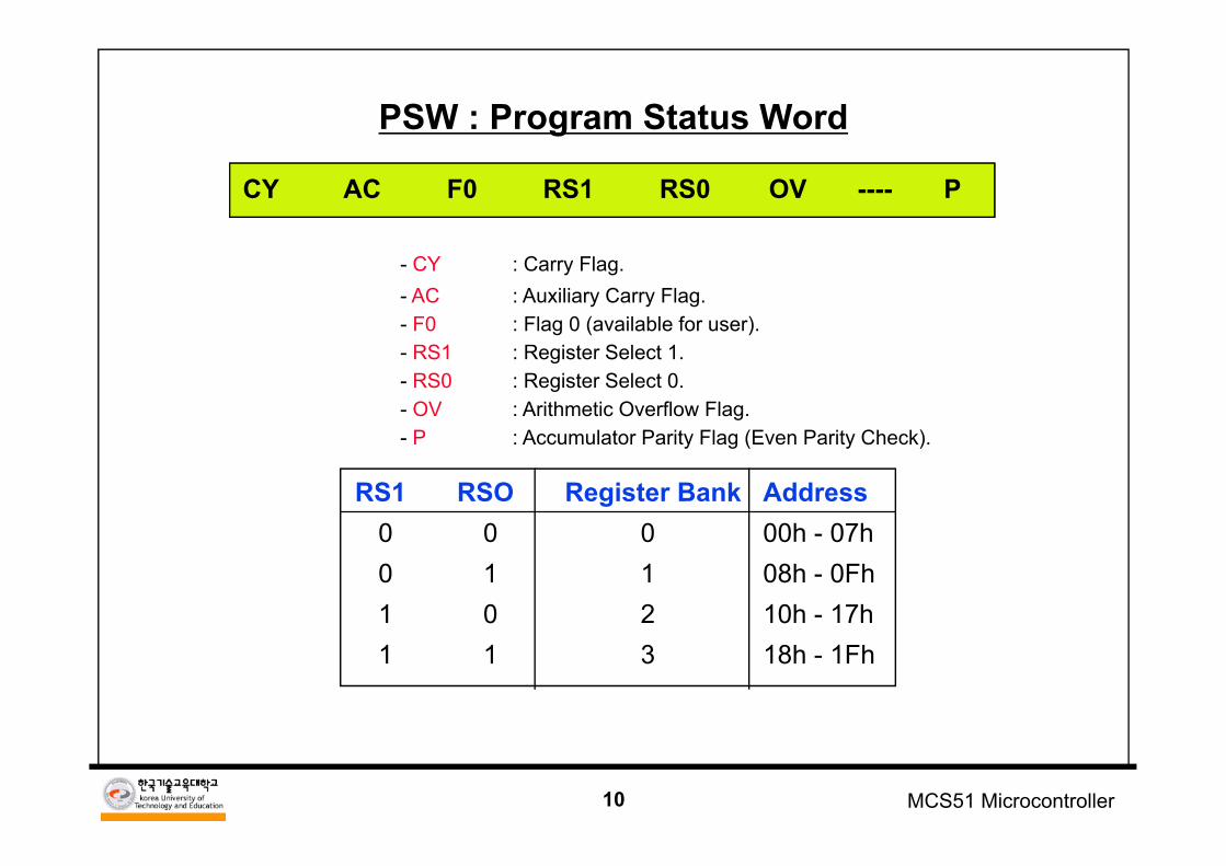
10 MCS51 Microcontroller
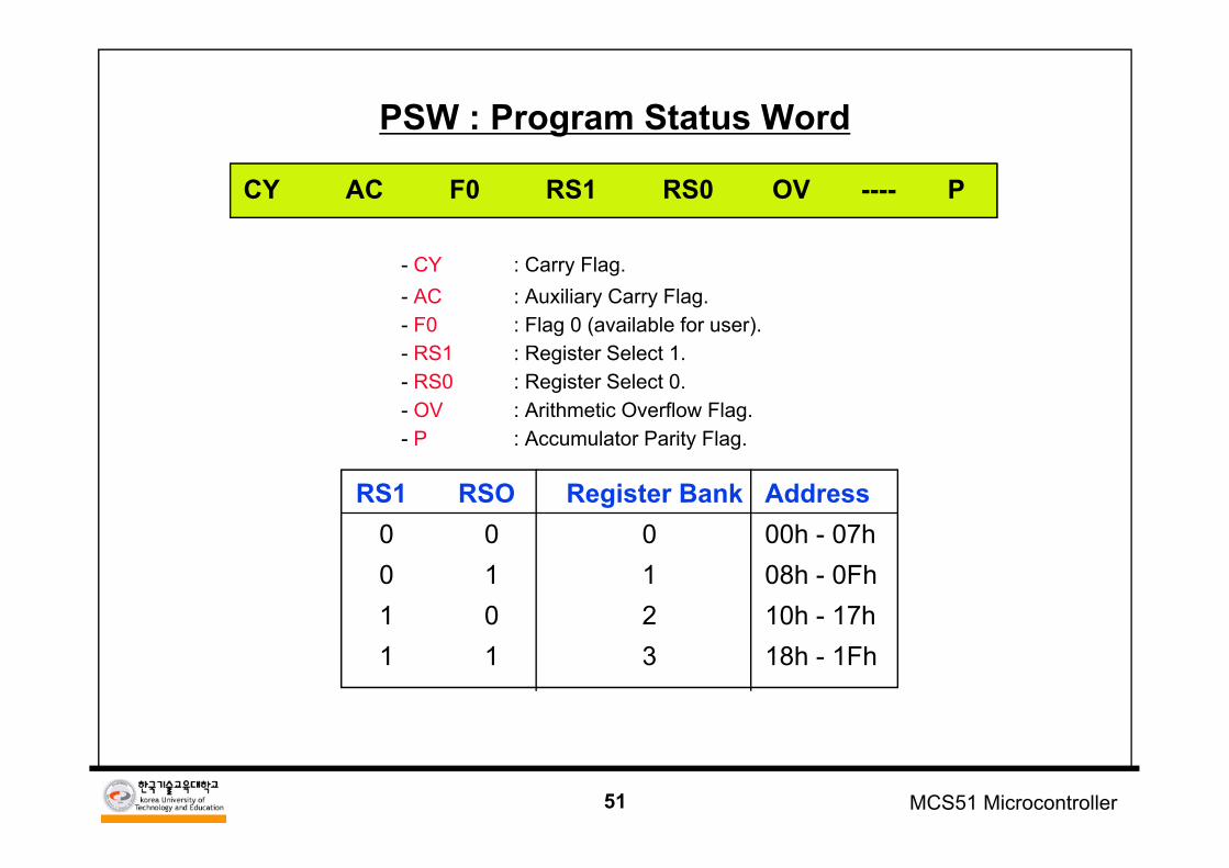
PSW : Program Status Word
CY AC F0 RS1 RS0 OV ---- P
- CY : Carry Flag.- AC : Auxiliary Carry Flag.- F0 : Flag 0 (available for user).- RS1 : Register Select 1.- RS0 : Register Select 0.- OV : Arithmetic Overflow Flag.- P : Accumulator Parity Flag (Even Parity Check).
RS1 RSO Register Bank Address0 0 0 00h - 07h0 1 1 08h - 0Fh1 0 2 10h - 17h1 1 3 18h - 1Fh
11 MCS51 Microcontroller
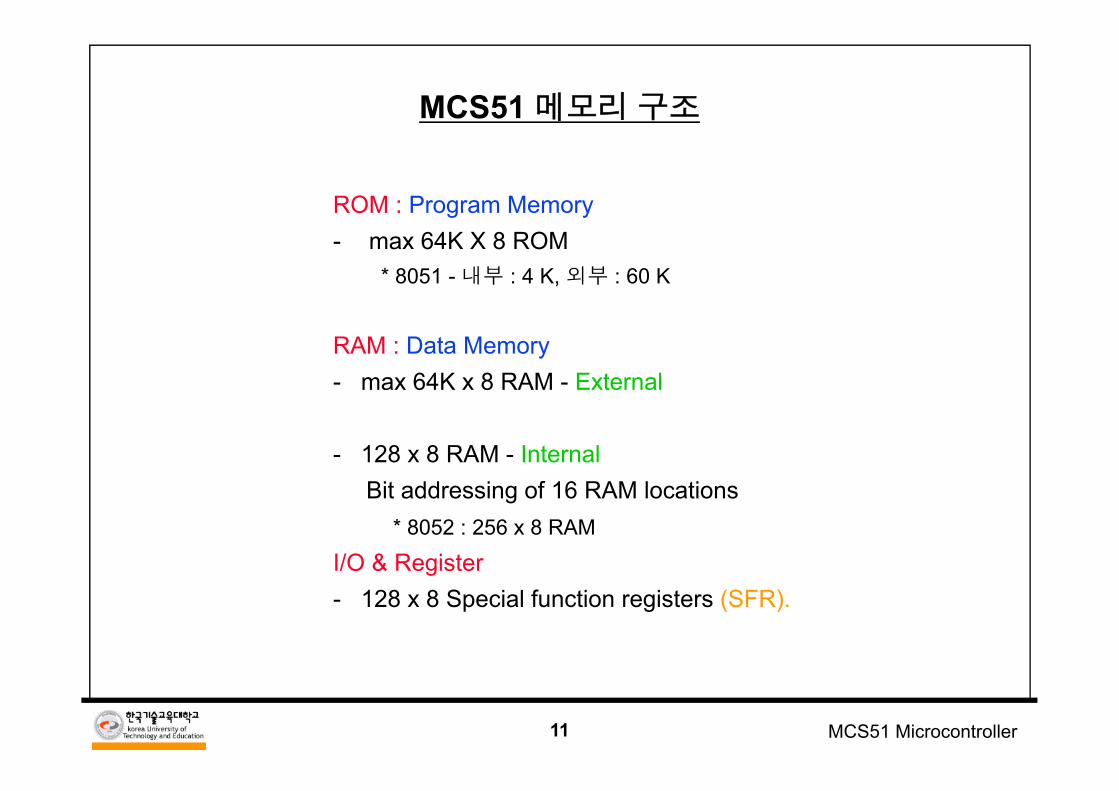
MCS51 메모리 구조
ROM : Program Memory- max 64K X 8 ROM
* 8051 - 내부 : 4 K, 외부 : 60 K
RAM : Data Memory- max 64K x 8 RAM - External
- 128 x 8 RAM - InternalBit addressing of 16 RAM locations
* 8052 : 256 x 8 RAM
I/O & Register- 128 x 8 Special function registers (SFR).
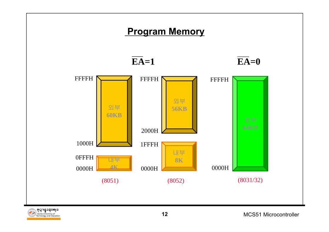
12 MCS51 Microcontroller
외부56KB
내부8K
FFFFH
2000H
1FFFH
0000H
외부60KB
내부4K
FFFFH
1000H
0FFFH
0000H
EA=1
외부64KB
FFFFH
0000H
EA=0
(8051) (8052)
Program Memory
(8031/32)
13 MCS51 Microcontroller
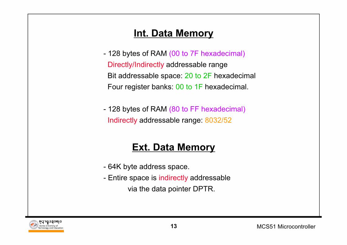
Int. Data Memory
- 128 bytes of RAM (00 to 7F hexadecimal)Directly/Indirectly addressable rangeBit addressable space: 20 to 2F hexadecimalFour register banks: 00 to 1F hexadecimal.
- 128 bytes of RAM (80 to FF hexadecimal)Indirectly addressable range: 8032/52
Ext. Data Memory
- 64K byte address space.- Entire space is indirectly addressable
via the data pointer DPTR.
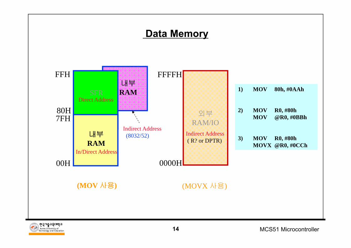
14 MCS51 Microcontroller
Data Memory
(MOV 사용) (MOVX 사용)
외부RAM/IO
내부RAM
SFR
0000H
FFFFH
00H
7FH
FFH
80H
Indirect Address(8032/52)
1) MOV 80h, #0AAh
2) MOV R0, #80h MOV @R0, #0BBh
3) MOV R0, #80h MOVX @R0, #0CCh
Direct Address
In/Direct Address
Indirect Address( R? or DPTR)
내부RAM
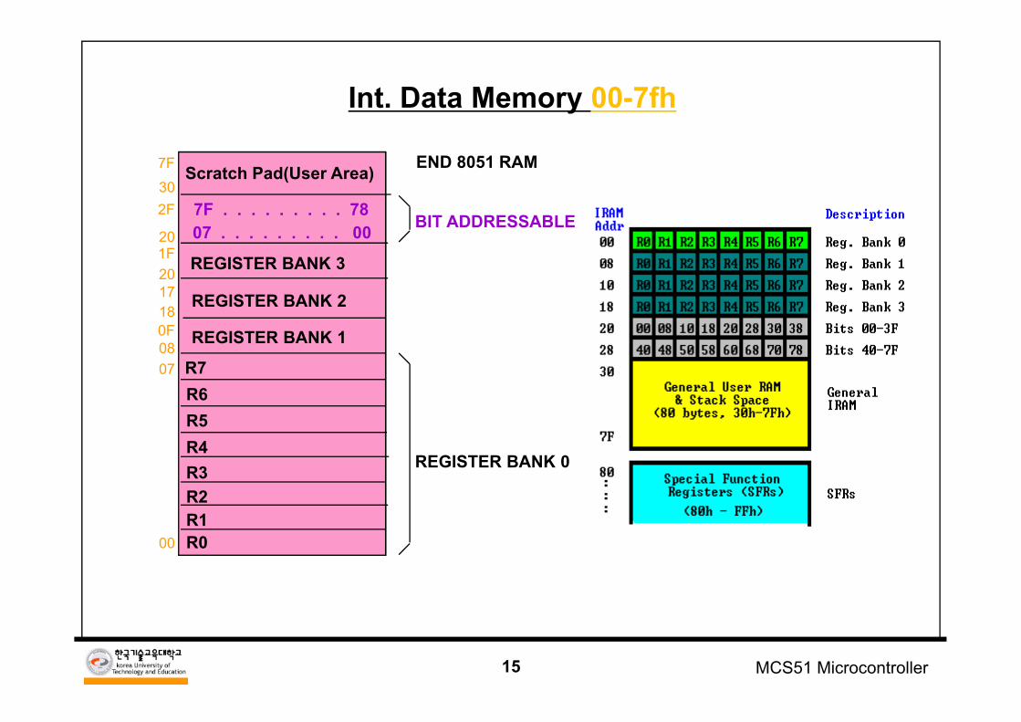
15 MCS51 Microcontroller
Int. Data Memory 00-7fh
R0R1R2R3R4R5R6R7
REGISTER BANK 1
REGISTER BANK 2
END 8051 RAM
BIT ADDRESSABLE
REGISTER BANK 3
7F302F
20
00
1F
0F
1718
0807
20
REGISTER BANK 0
07 . . . . . . . . . 007F . . . . . . . . . 78
Scratch Pad(User Area)
16 MCS51 Microcontroller
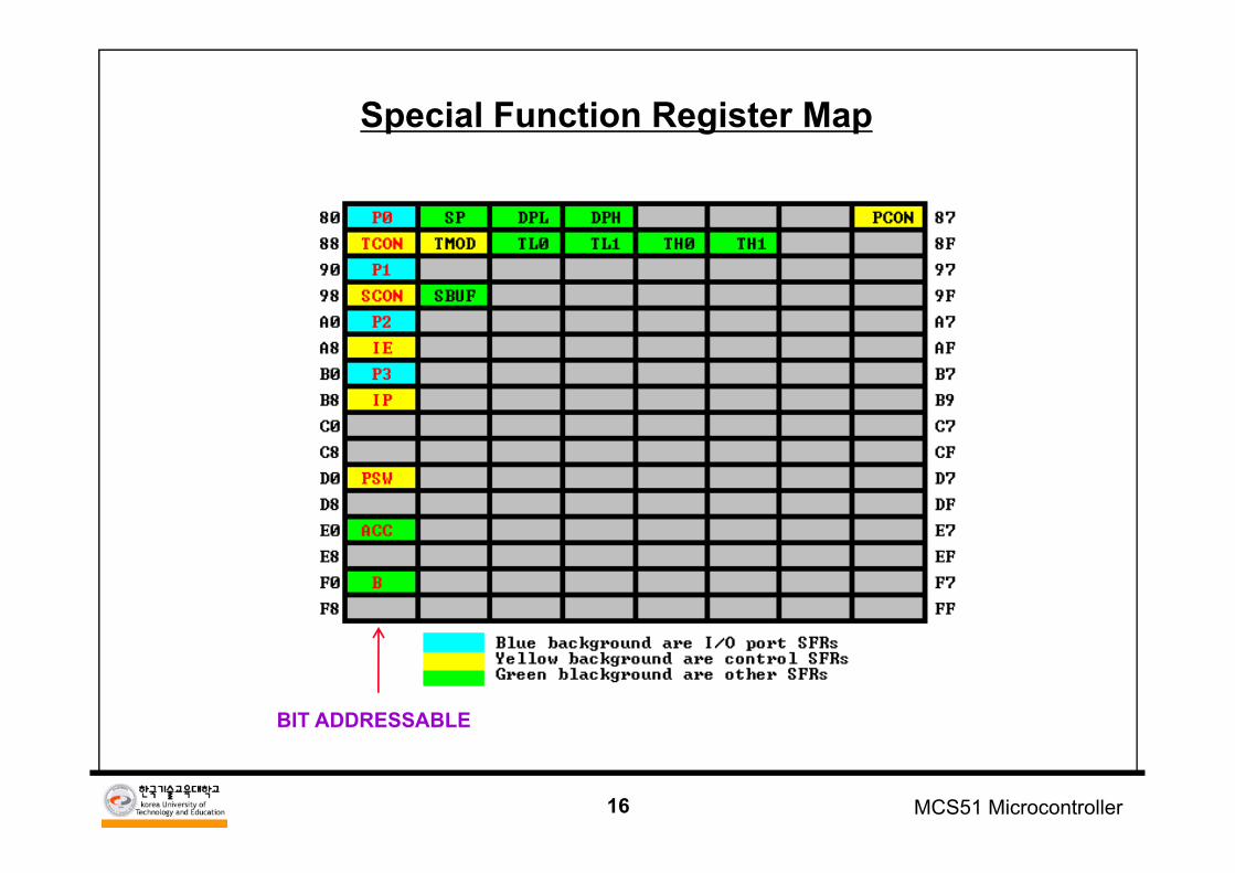
Special Function Register Map
BIT ADDRESSABLE
17 MCS51 Microcontroller
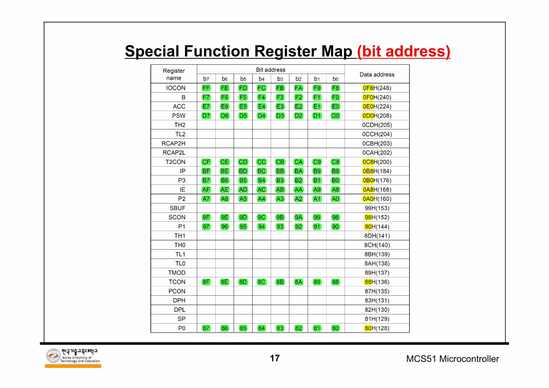
Special Function Register Map (bit address)
18 MCS51 Microcontroller
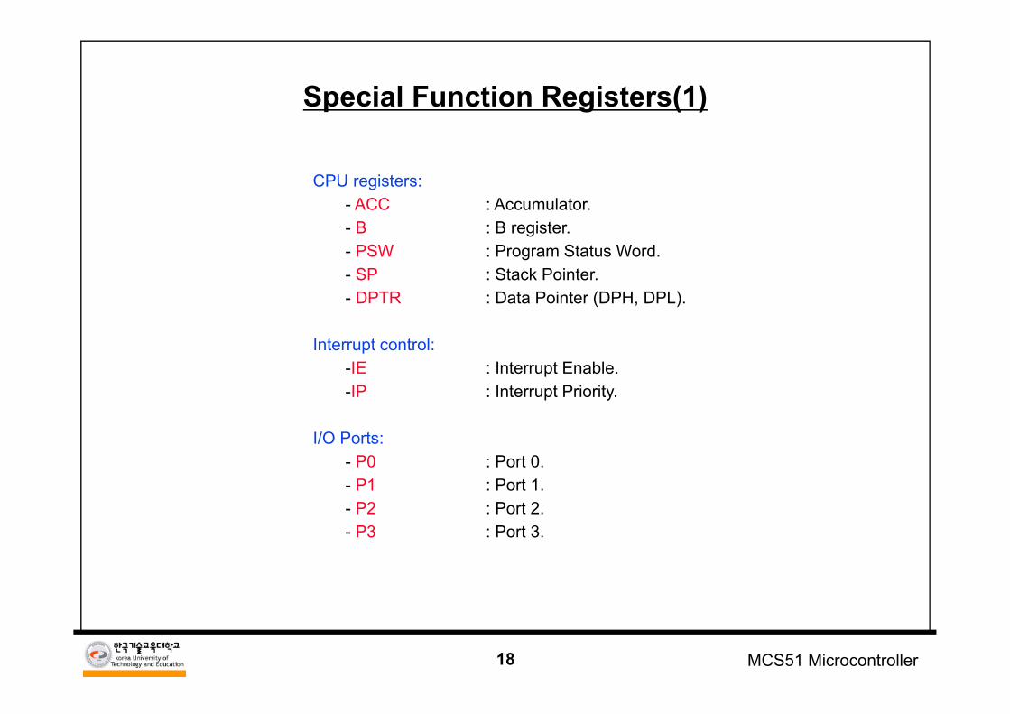
Special Function Registers(1)
CPU registers:- ACC : Accumulator.- B : B register.- PSW : Program Status Word.- SP : Stack Pointer.- DPTR : Data Pointer (DPH, DPL).
Interrupt control:-IE : Interrupt Enable.-IP : Interrupt Priority.
I/O Ports:- P0 : Port 0.- P1 : Port 1.- P2 : Port 2.- P3 : Port 3.
19 MCS51 Microcontroller
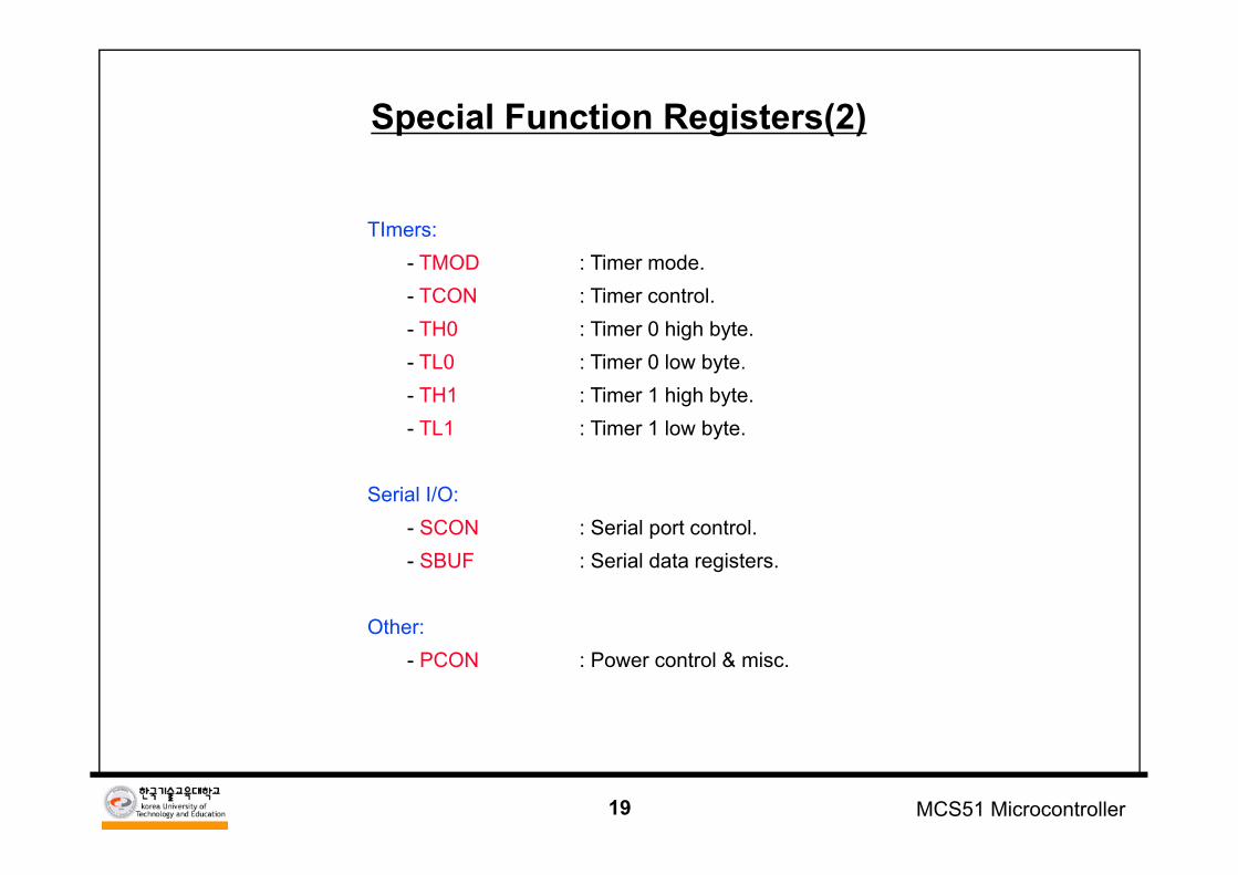
Special Function Registers(2)
TImers:- TMOD : Timer mode.- TCON : Timer control.- TH0 : Timer 0 high byte.- TL0 : Timer 0 low byte.- TH1 : Timer 1 high byte.- TL1 : Timer 1 low byte.
Serial I/O:- SCON : Serial port control.- SBUF : Serial data registers.
Other:- PCON : Power control & misc.

20 MCS51 Microcontroller
Memory & I/O Address Map
+ SFR : PIO, SIO, CTC
FFFFh
8000h
7FFFh
0000h
ROM
32K
MOVC
PSEN
FFFFh
C000h
8000h7FFFh
0000h
RAM 16K
Ext. I/O 16K
MOVX
RD / WR
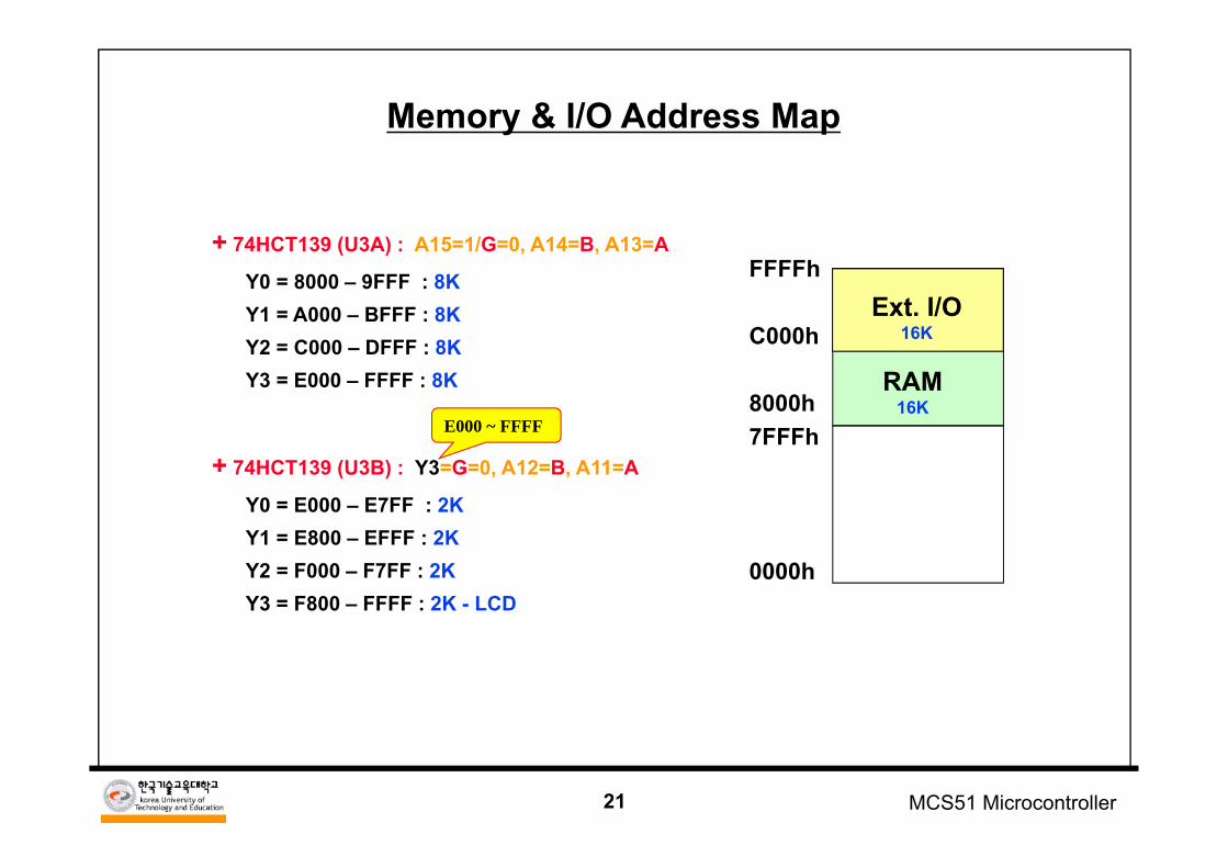
21 MCS51 Microcontroller
Memory & I/O Address Map
+ 74HCT139 (U3A) : A15=1/G=0, A14=B, A13=A
Y0 = 8000 – 9FFF : 8KY1 = A000 – BFFF : 8KY2 = C000 – DFFF : 8KY3 = E000 – FFFF : 8K
FFFFh
C000h
8000h7FFFh
0000h
RAM 16K
Ext. I/O 16K
+ 74HCT139 (U3B) : Y3=G=0, A12=B, A11=A
Y0 = E000 – E7FF : 2KY1 = E800 – EFFF : 2KY2 = F000 – F7FF : 2KY3 = F800 – FFFF : 2K - LCD
E000 ~ FFFF
22 MCS51 Microcontroller
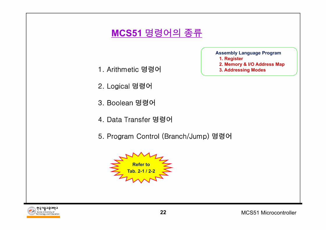
MCS51 명령어의 종류
1. Arithmetic 명령어
2. Logical 명령어
3. Boolean 명령어
4. Data Transfer 명령어
5. Program Control (Branch/Jump) 명령어
Refer to Tab. 2-1 / 2-2
Assembly Language Program1. Register2. Memory & I/O Address Map3. Addressing Modes
23 MCS51 Microcontroller
MCS51 Addressing Mode
- MOV A, R0 ; OP code, Destination Operand, Source Operand
- Memory Manipulation (Data Transfer)1. Immediate operands: {MOV A, #57h}, {MOV DPTR, #1234h}2. Register operands: R0 - R7 이용 {MOV R0, A} 3. Direct Operands: {MOV A, 40h}, {MOV 50h, 30h}, {MOV P1, #55h}, {MOV A, P1}4. Register Indirect :
* RAM내부 : MOV @R0, A외부 RAM or I/O: MOVX A, @DPTR
5. Base register (DPTR/PC) + Index register (A)* ROM : MOVC A, @A+DPTR / MOVC A, @A+PC
- Branch (Unconditional)1. Absolute : 11 bit address (2K byte 이내) = AJMP xxx2. Relative(short) : 8 bit address (+127 ~ -128) = SJMP xx3. Long : 16 bit address (64K byte) = LJMP xxxx4. Base register (DPTR) + Index register (A) = JMP @A+DPTR
- Branch (Conditional)JC, JNC JZ, JNZDJNZ CJNE
24 MCS51 Microcontroller
Arithmetic 명령어
Mnemonics Operands Bytes/Cycles
ADD A, Rn 1/1ADDC A, direct 2/1SUBB A, @Ri 1/1
A, #data 2/1
INC A 1/1DEC Rn 1/1
direct 2/1@Ri 1/1
INC DPTR 1/2MUL AB 1/4DIV AB 1/4DA A 1/1
25 MCS51 Microcontroller
SUBB 명령어
SUBB A, #35h : Subtract with borrow ( A = 22h)SUBtract with Borrow = SUBB
(+ 22h) 0 0 1 0 0 0 1 0
- (+ 35h) - 0 0 1 1 0 1 0 1
EDh 1 1 1 0 1 1 0 1
EDh - 1 (C) = ECh
CY AC F0 RS1 RS0 OV ---- P
1 x x x1 1 0 1
BeforeAfter
26
Hexadecimal : CY=0, A=9Bh
Decimal : CY=1, A=01
MCS51 Microcontroller
DA A 명령어
MOV A, #34hADD A, #67h
MOV A, #34hADD A, #67hDA A
0011 0100 ( 34h )
+ 0110 0111 ( 67h )
1001 1011 ( 9Bh )
CY =0 AC=0
1001 1011 ( 9Bh )
+ 0110 0110 ( 66h ) ; adjust 66h
0000 0001 ( 01 )
CY =1 AC=1
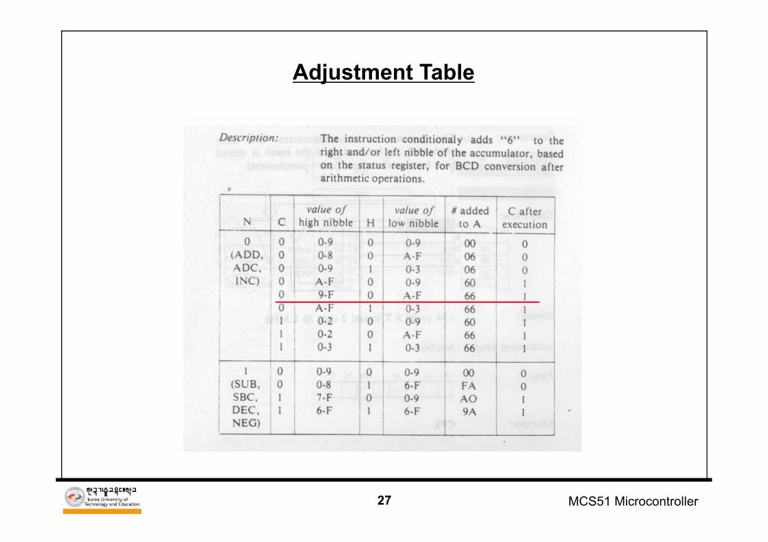
27 MCS51 Microcontroller
Adjustment Table
28 MCS51 Microcontroller
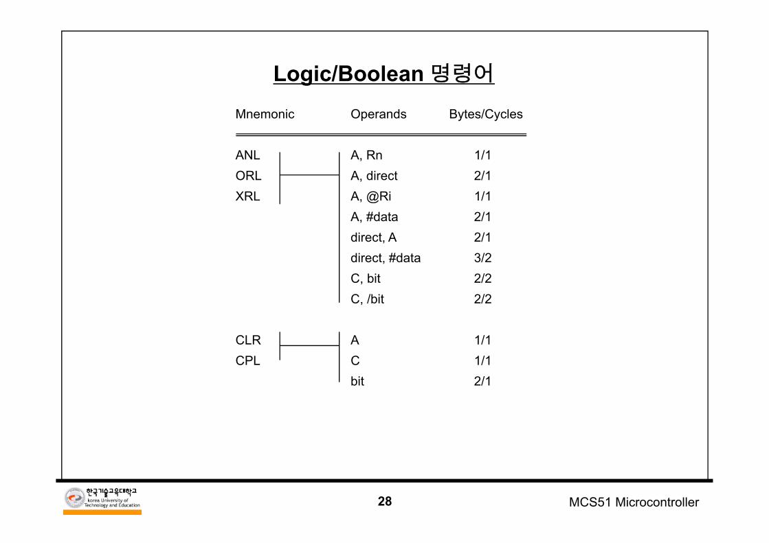
Logic/Boolean 명령어
Mnemonic Operands Bytes/Cycles
ANL A, Rn 1/1ORL A, direct 2/1XRL A, @Ri 1/1
A, #data 2/1direct, A 2/1direct, #data 3/2C, bit 2/2C, /bit 2/2
CLR A 1/1CPL C 1/1
bit 2/1
29 MCS51 Microcontroller
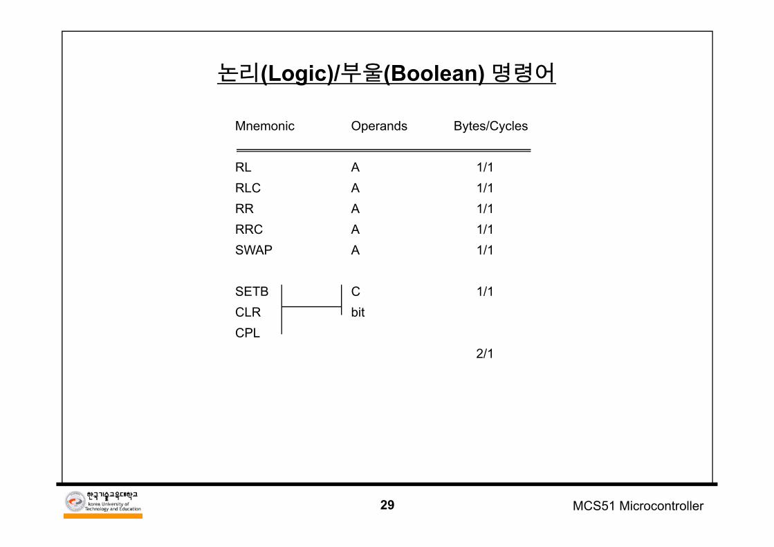
논리(Logic)/부울(Boolean) 명령어
Mnemonic Operands Bytes/Cycles
RL A 1/1RLC A 1/1RR A 1/1RRC A 1/1SWAP A 1/1
SETB C 1/1CLR bitCPL
2/1
30 MCS51 Microcontroller
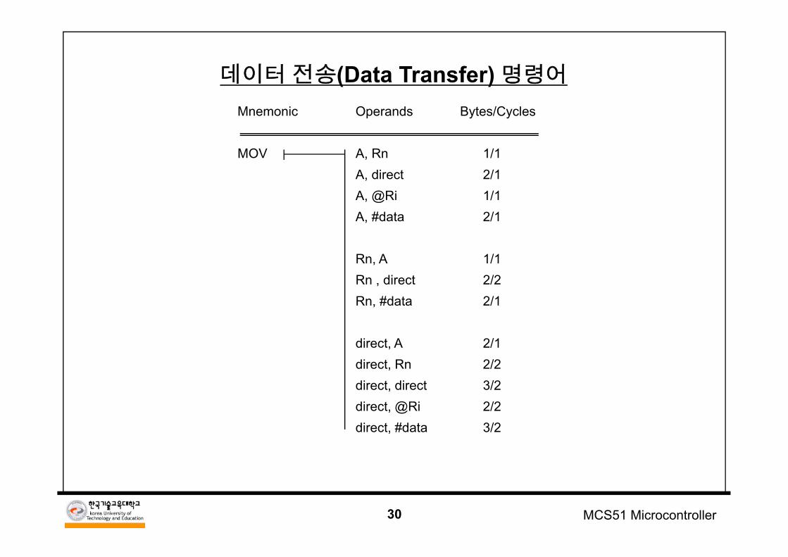
데이터 전송(Data Transfer) 명령어
Mnemonic Operands Bytes/Cycles
MOV A, Rn 1/1A, direct 2/1A, @Ri 1/1A, #data 2/1
Rn, A 1/1Rn , direct 2/2Rn, #data 2/1
direct, A 2/1direct, Rn 2/2direct, direct 3/2direct, @Ri 2/2direct, #data 3/2
31 MCS51 Microcontroller
데이터 전송(Data Transfer) 명령어
Mnemonic Operands Bytes/Cycles
MOV @Ri, A 1/1@Ri, direct 2/2@Ri, #data 2/1
DPTR, #data16 3/2
C, bit 2/1bit, C 2/2
MOVX A,@DPTR 1/2@DPTR,A 1/2A,@Ri 1/2@Ri,A 1/2
32 MCS51 Microcontroller
데이터 전송(Data Transfer) 명령어
Mnemonic Operands Bytes/Cycles
MOVC A, @A+DPTR 1/2A, @A+PC 1/2
PUSH direct 2/2POP direct 2/2
XCH A, Rn 1/1A, direct 2/1A, @Ri 1/1
XCHD A, @Ri 1/1
33 MCS51 Microcontroller
분기(Branch) 명령어
Mnemonic Operands Bytes/Cycles
LCALL addr16 3/2ACALL addr11 2/2RET - 1/2RETI - 1/2LJMP addr16 3/2AJMP addr11 2/2SJMP rel 2/2JMP @A+DPTR 1/2JZ rel 2/2JNZ rel 2/2
34 MCS51 Microcontroller
분기(Branch) 명령어
ACALL addr11
Example) ACALL 0345h
0121 71 450123 …..
012101220123
7145
Memory
PC = 0123 → 0000 0001 0010 0011Addr11 = 0345 → 0000 0011 0100 0101
0345 ← 0000 0011 0100 0101
page
11 bits
Addr11 = 0345 → 0000 0011 0100 0101OP Code = a10..8 1 0 0 0 1 a7..0 7145 ← 0 1 1 1 0 0 0 1 0 1 0 0 0 1 0 1
35 MCS51 Microcontroller
분기(Branch) 명령어
AJMP addr11 ACALL addr11
Example) AJMP 01D2h
083F 21 D20841 …..
083F08400841
21D2
Memory
PC = 0841 → 0000 1000 0100 0001Addr11 = 01D2 → 0000 0001 1011 0010
09D2 ← 0000 1001 1011 0010
page
11 bits
Example) ACALL 0137h
0132 31 370134 …..
013201330134
3137
Memory
PC = 0134 → 0000 0001 0011 0100Addr11 = 0137 → 0000 0001 0011 0111
0137 ← 0000 0001 0011 0111
page
11 bits
36 MCS51 Microcontroller
분기(Branching) 명령어
Mnemonic Operands Bytes/Cycles
CJNE A, direct, rel 3/2A, #data, rel 3/2Rn, #data, rel 3/2@Ri,#data,rel 3/2
DJNZ Rn, rel 2/2direct, rel 3/2
NOP - 1/1JC rel 2/2JNC rel 2/2JB bit, rel 3/2JNB bit, rel 3/2JBC bit, rel 3/2
37 MCS51 Microcontroller
MCS51 Pin 기능
VSS VCC RST
P0.7P0.6P0.5P0.4P0.3P0.2P0.1P0.0
PO RT0
ADDRESS ANDDATA BUS
XTAL1
XTAL2
ALE
EA
PSEN
P3.7P3.6P3.5P3.4P3.3P3.2P3.1P3.0
SECONDARYFUNCTIONS
RxD TxD INT0INT1T0T1WRRD
PORT3
P2.7P2.6P2.5P2.4P2.3P2.2P2.1P2.0
PORT2
ADDRESSBUS
P1.7P1.6P1.5P1.4P1.3P1.2P1.1P1.0
PORT1
AD0 ~ AD7
A8 ~ A15
SECONDARYFUNCTIONS
38 MCS51 Microcontroller
VIH = 2.5V
Time Period = 0.75RC
Cold Reset
Power-On
Min. 24 Clocks
Warm Reset
Reset S/W
Min. 24 Clocks
MCS51 Reset Timing
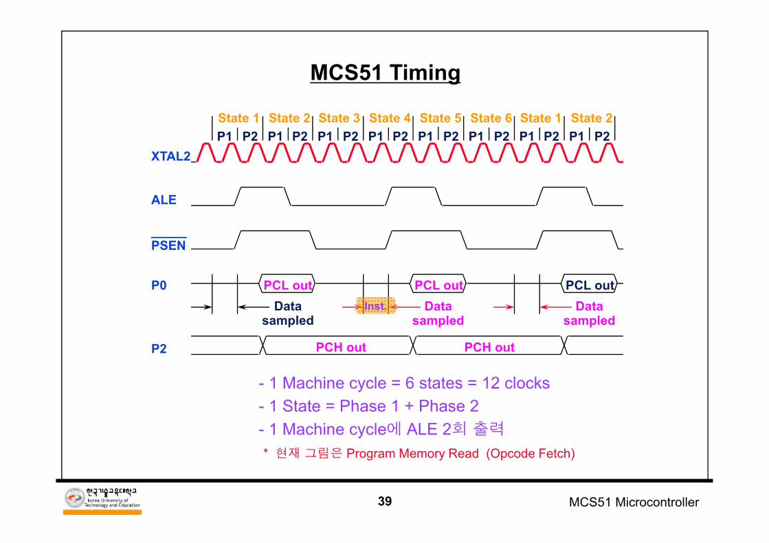
39 MCS51 Microcontroller
MCS51 Timing
State 1 State 2 State 3 State 4 State 5 State 6 State 1 State 2
XTAL2
ALE
_____PSEN
P0
P2
Datasampled
PCL out PCL outData
sampled
PCL outData
sampled
PCH out PCH out
P1 P2 P1 P2 P1 P2 P1 P2 P1 P2 P1 P2 P1 P2 P1 P2
- 1 Machine cycle = 6 states = 12 clocks- 1 State = Phase 1 + Phase 2- 1 Machine cycle에 ALE 2회 출력
* 현재 그림은 Program Memory Read (Opcode Fetch)
Inst.
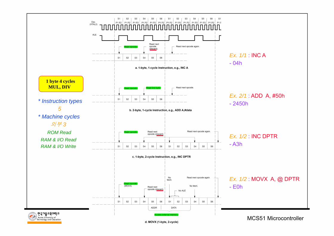
40 MCS51 Microcontroller
Ex. 1/1 : INC A- 04h
Ex. 2/1 : ADD A, #50h- 2450h
Ex. 1/2 : INC DPTR- A3h
Ex. 1/2 : MOVX A, @ DPTR- E0h
1 byte 4 cyclesMUL, DIV
* Instruction types5
* Machine cycles외부 3
ROM ReadRAM & I/O ReadRAM & I/O Write
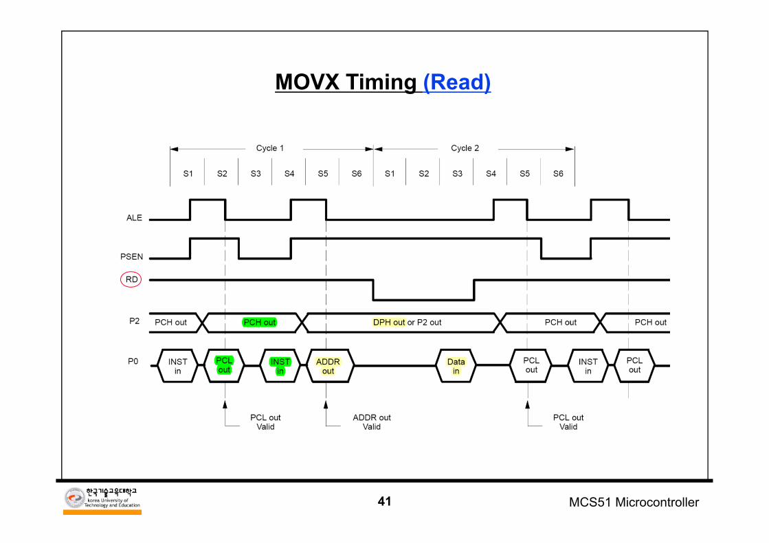
41 MCS51 Microcontroller
MOVX Timing (Read)
42 MCS51 Microcontroller
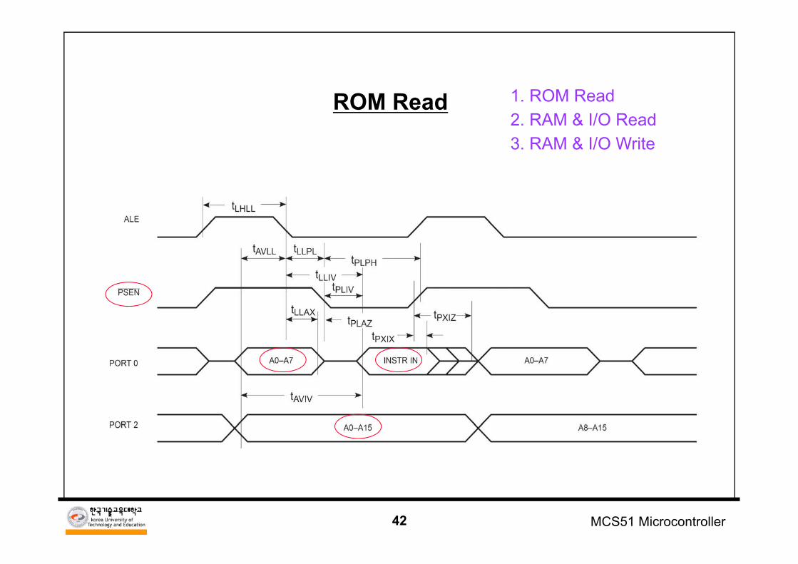
ROM Read 1. ROM Read2. RAM & I/O Read3. RAM & I/O Write
43 MCS51 Microcontroller
RAM & I/O Read
44 MCS51 Microcontroller
RAM & I/O Write
45 MCS51 Microcontroller
외부 장치와의 인터페이스
8051PORT 2
PORT 0
ALE
P3.7
P3.6
PSEN
A15 - A8: High byte of address
AD7 - AD0: Data and low byteaddress
ALE: Address latch enable
RD: Read strobe (RAM or I/O Read)
WR: Write strobe (RAM or I/O Write)
PSEN: Program store enable (ROM Read)
46 MCS51 Microcontroller
외부 ROM 인터페이스
8051PORT2
ALE
PORT0
ADDRESSLATCH
ROM
ADDRESS INPUTS
DATA OUTPUTS
OE (RD)PSEN
A15 - A8
A7 - A0
D7 - D0
AD7 - AD0
47 MCS51 Microcontroller
8051PORT 2
ALE
PORT 0DATA OUTPUTS
ADDRESS LATCH
DECODE CE
WE (WR)OE (RD)
WRRD
외부 RAM및 I/O 장치 인터페이스
- 64K byte address space.- Entire space in indirectly addressable
via the data pointer DPTR and MOVX.
RAM or I/O
ADDRESSINPUTS
A15 - A8
AD7 - AD0
D7 - D0
A7 - A0
48 MCS51 Microcontroller
Memory & I/O Address Map
+ SFR : PIO, SIO, CTC
FFFFh
8000h
7FFFh
0000h
ROM
32K
MOVC
PSEN
FFFFh
C000h
8000h7FFFh
0000h
RAM 16K
Ext. I/O 16K
MOVX
RD / WR
49 MCS51 Microcontroller
RAM & I/O Address Map
+ 74HCT139 (U3A) : A15=1/G=0, A14=B, A13=A
Y0 = 8000 – 9FFF : 8KY1 = A000 – BFFF : 8KY2 = C000 – DFFF : 8KY3 = E000 – FFFF : 8K
FFFFh
C000h
8000h7FFFh
0000h
RAM 16K
Ext. I/O 16K
+ 74HCT139 (U3B) : Y3=G=0, A12=B, A11=A
Y0 = E000 – E7FF : 2KY1 = E800 – EFFF : 2KY2 = F000 – F7FF : 2KY3 = F800 – FFFF : 2K - LCD
E000 ~ FFFF
RAM8000 – BFFF
C000 – FFFF I/O
50 MCS51 Microcontroller
Final Address Map
RAM
FFFFh
C000h
8000h7FFFh
0000h
ROM
Ext. I/O
A15 A14 A13 A12
1 0 0 x Y0
1 0 1 x Y1
1 1 0 x Y2
1 1 1 x Y3
8000 – BFFFF
C000 – FFFF I/ORAM
A15 A14 A13 A12 A11
1 1 1 0 0 Y0
1 1 1 0 1 Y1
1 1 1 1 0 Y2
1 1 1 1 1 Y3
E000hE800hF000hF800h
51 MCS51 Microcontroller
PSW : Program Status Word
CY AC F0 RS1 RS0 OV ---- P
- CY : Carry Flag.- AC : Auxiliary Carry Flag.- F0 : Flag 0 (available for user).- RS1 : Register Select 1.- RS0 : Register Select 0.- OV : Arithmetic Overflow Flag.- P : Accumulator Parity Flag.
RS1 RSO Register Bank Address0 0 0 00h - 07h0 1 1 08h - 0Fh1 0 2 10h - 17h1 1 3 18h - 1Fh
52 MCS51 MicrocontrollerMCS51 Microcontroller
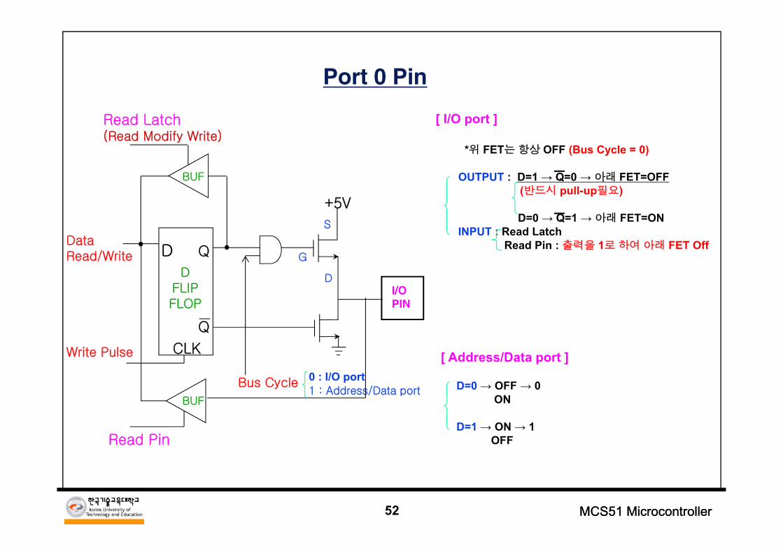
Port 0 Pin
0 : I/O port1 : Address/Data port
DFLIPFLOP
QD
Q
CLK
+5V
BUF
BUF
G
S
D
Read Latch(Read Modify Write)
Read Pin
Data Read/Write
Write Pulse
Bus Cycle
[ Address/Data port ]
D=0 → OFF → 0ON
D=1 → ON → 1OFF
[ I/O port ]
*위 FET는 항상 OFF (Bus Cycle = 0)
OUTPUT : D=1 → Q=0 → 아래 FET=OFF(반드시 pull-up필요)
D=0 → Q=1 → 아래 FET=ONINPUT : Read Latch
Read Pin : 출력을 1로 하여 아래 FET Off
I/OPIN
53 MCS51 Microcontroller
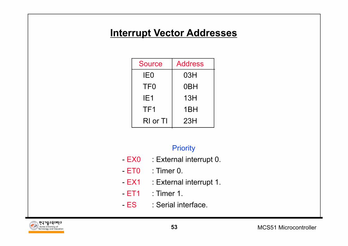
Interrupt Vector Addresses
Source AddressIE0 03HTF0 0BHIE1 13HTF1 1BHRI or TI 23H
Priority- EX0 : External interrupt 0.- ET0 : Timer 0.- EX1 : External interrupt 1.- ET1 : Timer 1.- ES : Serial interface.
54 MCS51 Microcontroller
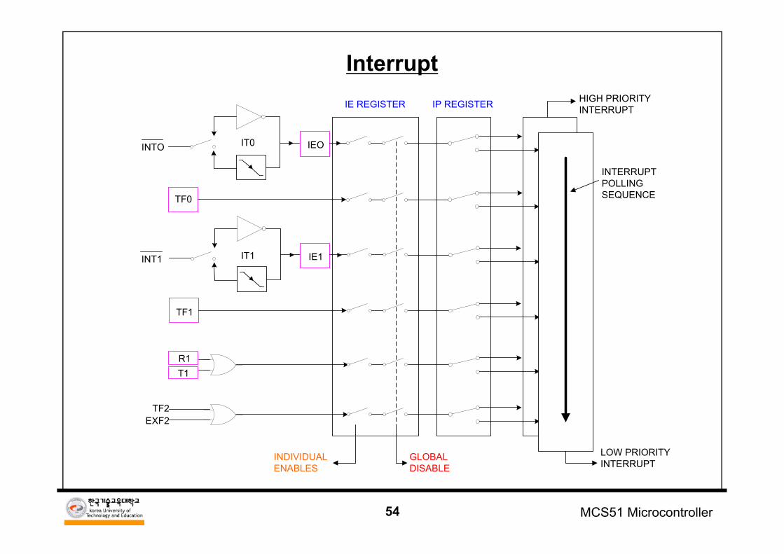
Interrupt
INTO
TF0
TF1
T1R1
IEO
IE1INT1
EXF2TF2
IT0
IT1
IE REGISTER IP REGISTER HIGH PRIORITYINTERRUPT
INTERRUPTPOLLINGSEQUENCE
LOW PRIORITYINTERRUPT
GLOBALDISABLE
INDIVIDUALENABLES
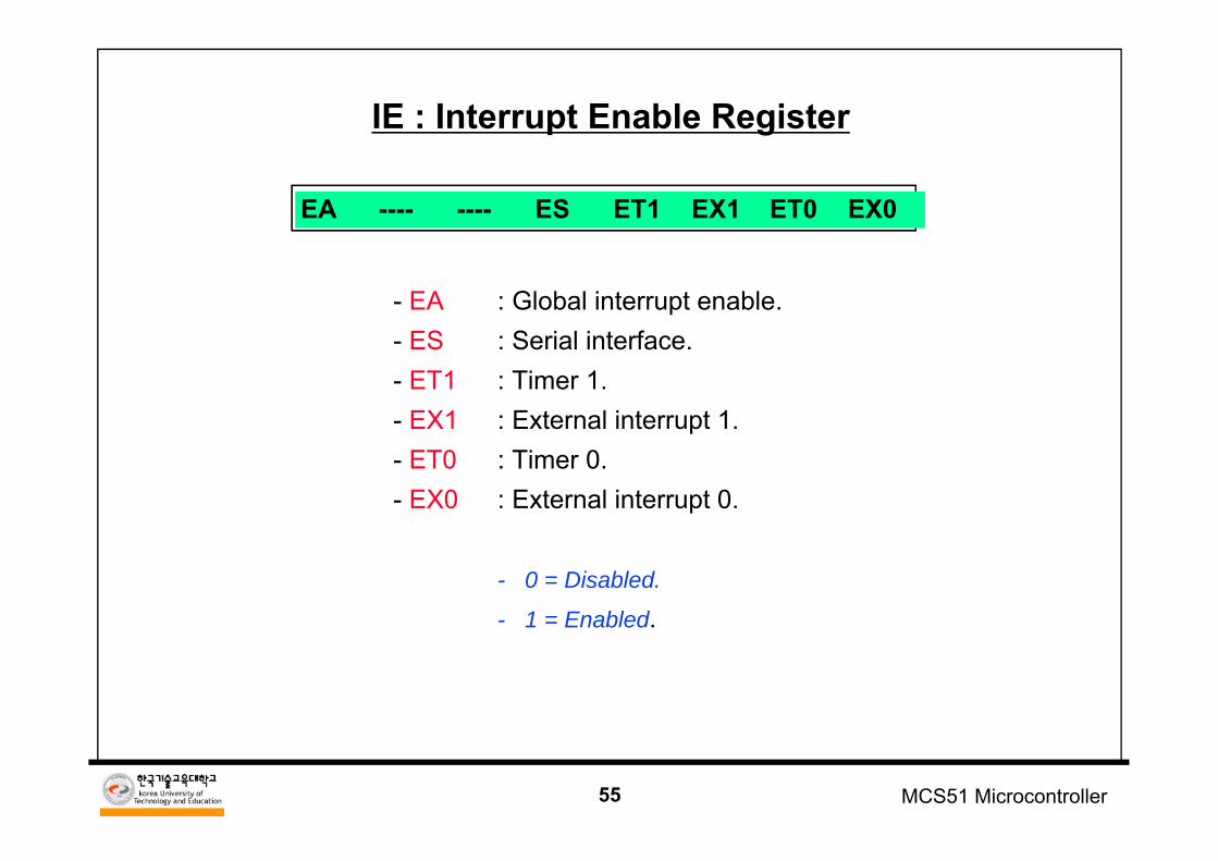
55 MCS51 Microcontroller
IE : Interrupt Enable Register
- EA : Global interrupt enable.- ES : Serial interface.- ET1 : Timer 1.- EX1 : External interrupt 1.- ET0 : Timer 0.- EX0 : External interrupt 0.
- 0 = Disabled.
- 1 = Enabled.
EA ---- ---- ES ET1 EX1 ET0 EX0
56 MCS51 Microcontroller
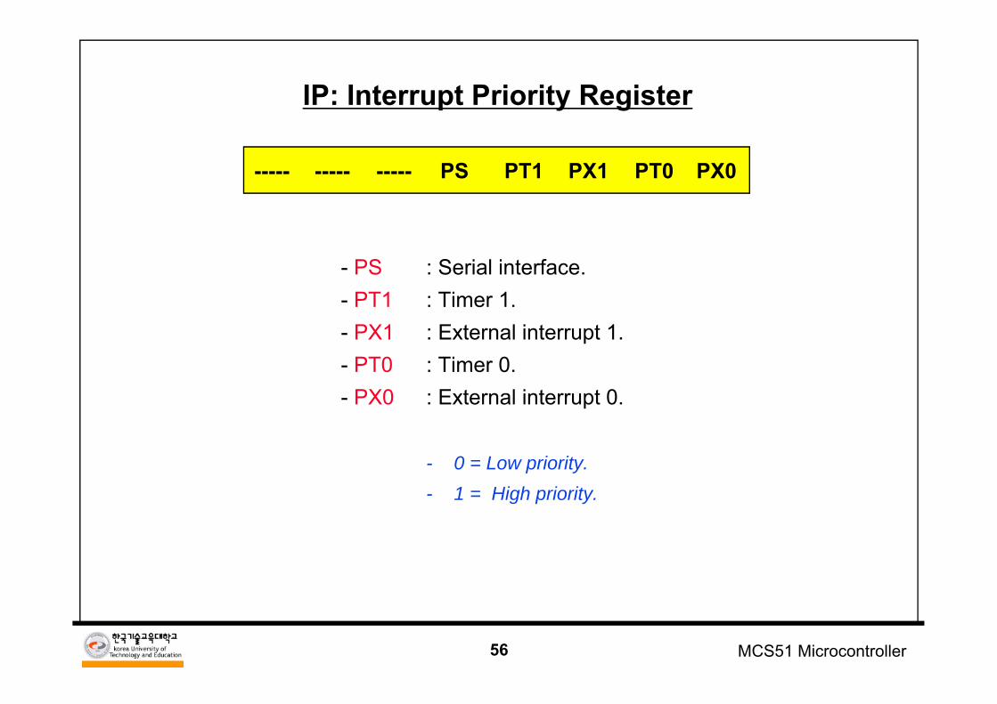
IP: Interrupt Priority Register
- PS : Serial interface.- PT1 : Timer 1.- PX1 : External interrupt 1.- PT0 : Timer 0.- PX0 : External interrupt 0.
- 0 = Low priority.- 1 = High priority.
----- ----- ----- PS PT1 PX1 PT0 PX0
57 MCS51 Microcontroller
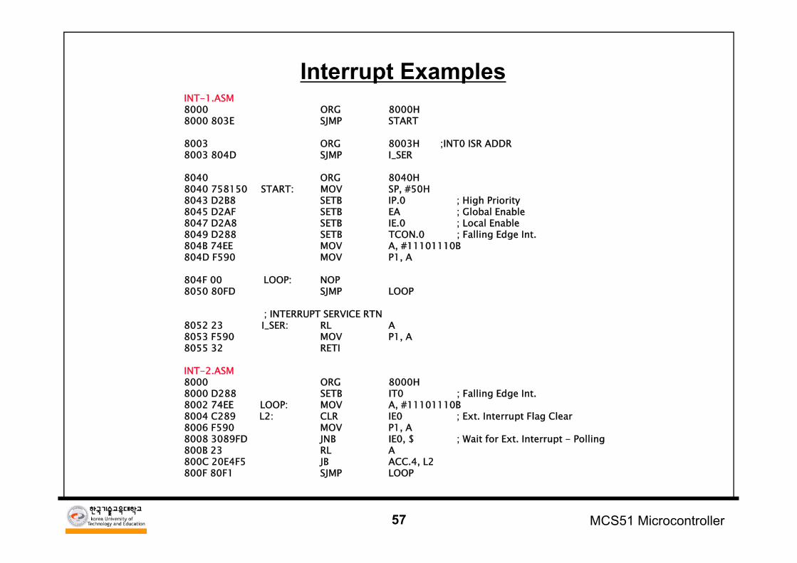
Interrupt ExamplesINT-1.ASM 8000 ORG 8000H8000 803E SJMP START
8003 ORG 8003H ;INT0 ISR ADDR8003 804D SJMP I_SER
8040 ORG 8040H8040 758150 START: MOV SP, #50H8043 D2B8 SETB IP.0 ; High Priority8045 D2AF SETB EA ; Global Enable8047 D2A8 SETB IE.0 ; Local Enable8049 D288 SETB TCON.0 ; Falling Edge Int.804B 74EE MOV A, #11101110B804D F590 MOV P1, A
804F 00 LOOP: NOP8050 80FD SJMP LOOP
; INTERRUPT SERVICE RTN8052 23 I_SER: RL A8053 F590 MOV P1, A8055 32 RETI
INT-2.ASM8000 ORG 8000H8000 D288 SETB IT0 ; Falling Edge Int.8002 74EE LOOP: MOV A, #11101110B8004 C289 L2: CLR IE0 ; Ext. Interrupt Flag Clear8006 F590 MOV P1, A 8008 3089FD JNB IE0, $ ; Wait for Ext. Interrupt - Polling800B 23 RL A800C 20E4F5 JB ACC.4, L2800F 80F1 SJMP LOOP
58 MCS51 Microcontroller
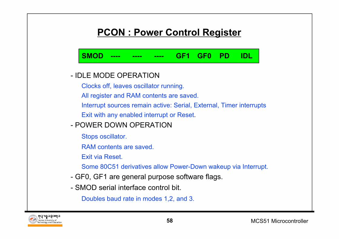
PCON : Power Control Register
- IDLE MODE OPERATIONClocks off, leaves oscillator running.All register and RAM contents are saved.Interrupt sources remain active: Serial, External, Timer interruptsExit with any enabled interrupt or Reset.
- POWER DOWN OPERATIONStops oscillator.RAM contents are saved.Exit via Reset.Some 80C51 derivatives allow Power-Down wakeup via Interrupt.
- GF0, GF1 are general purpose software flags.- SMOD serial interface control bit.
Doubles baud rate in modes 1,2, and 3.
SMOD ---- ---- ---- GF1 GF0 PD IDL
59 MCS51 Microcontroller
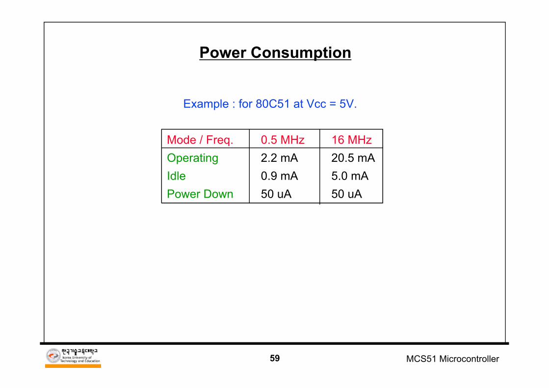
Power Consumption
Example : for 80C51 at Vcc = 5V.
Mode / Freq. 0.5 MHz 16 MHzOperating 2.2 mA 20.5 mAIdle 0.9 mA 5.0 mAPower Down 50 uA 50 uA
60 MCS51 Microcontroller
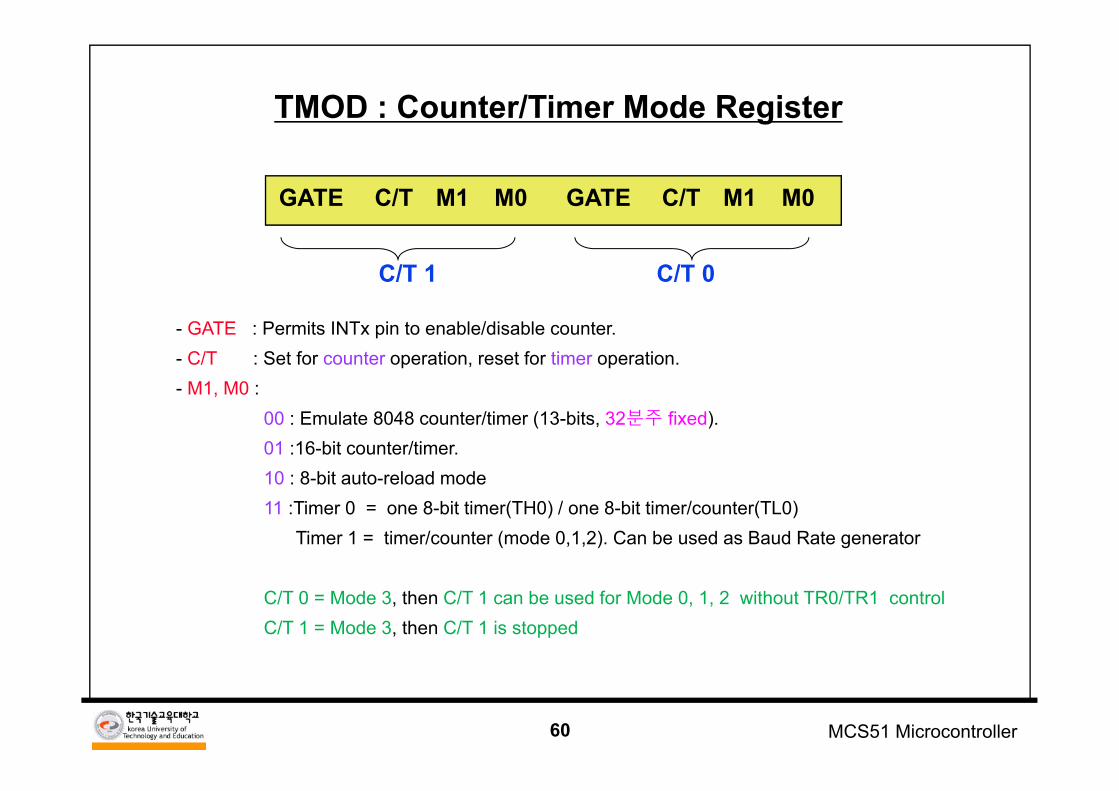
TMOD : Counter/Timer Mode Register
GATE C/T M1 M0 GATE C/T M1 M0
C/T 1 C/T 0
- GATE : Permits INTx pin to enable/disable counter.- C/T : Set for counter operation, reset for timer operation.- M1, M0 :
00 : Emulate 8048 counter/timer (13-bits, 32분주 fixed).01 :16-bit counter/timer.10 : 8-bit auto-reload mode11 :Timer 0 = one 8-bit timer(TH0) / one 8-bit timer/counter(TL0)
Timer 1 = timer/counter (mode 0,1,2). Can be used as Baud Rate generator
C/T 0 = Mode 3, then C/T 1 can be used for Mode 0, 1, 2 without TR0/TR1 controlC/T 1 = Mode 3, then C/T 1 is stopped
61 MCS51 Microcontroller
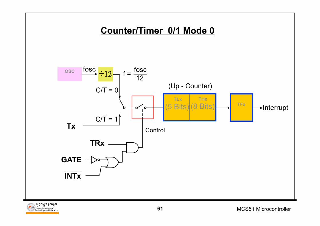
Counter/Timer 0/1 Mode 0
Interrupt
OSCOSC
TLx
(5 Bits) TFxTHx
(8 Bits)
Tx Control
C/T = 0
C/T = 1
f = 12foscfosc
÷12
INTx
GATE
TRx
(Up - Counter)
62 MCS51 Microcontroller
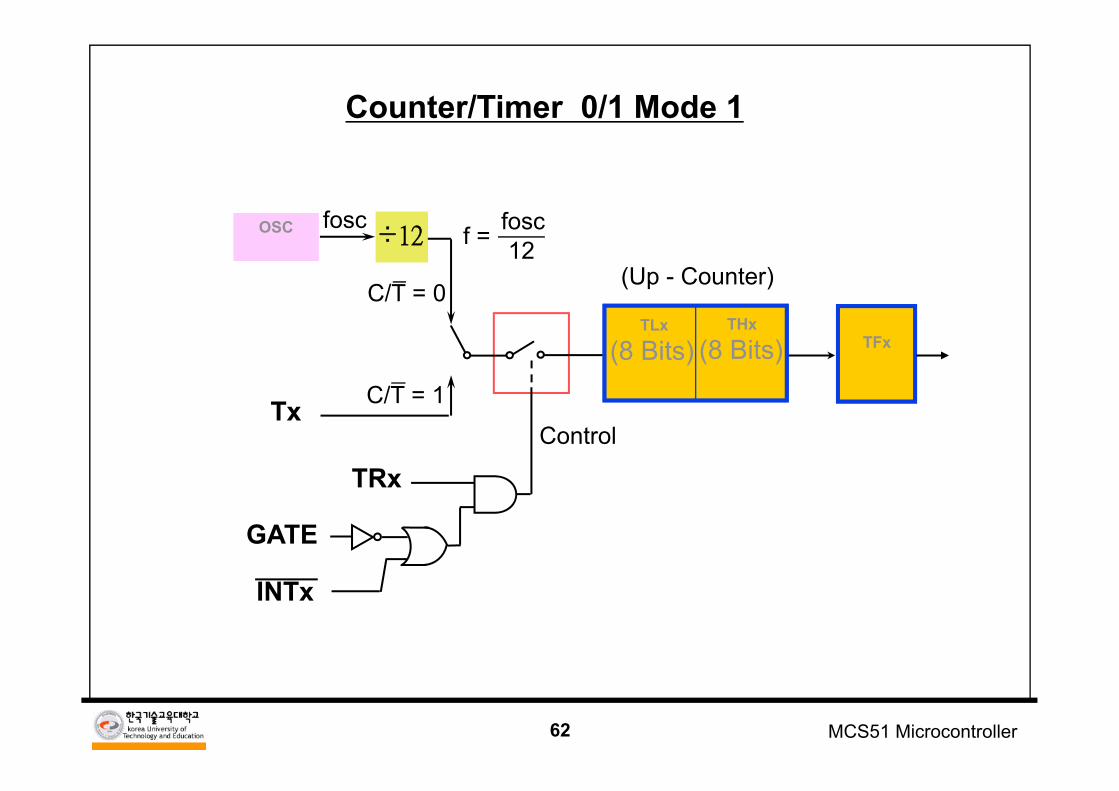
Counter/Timer 0/1 Mode 1
OSCOSC
TLx
(8 Bits) TFxTHx
(8 Bits)
TxControl
C/T = 0
C/T = 1
f = 12foscfosc
÷12
INTx
GATE
TRx
(Up - Counter)
63 MCS51 Microcontroller
Counter/Timer 0/1 Mode 2
THx
(8 Bits)
Interrupt
OSCOSC
TLx
(8 Bits) TFx
TxControl
C/T = 0
C/T = 1
f = 12foscfosc
÷12
INTx
GATE
TRx
(Up - Counter)
Reload
64 MCS51 Microcontroller
Counter/Timer 0 Mode 3 (T0)
TH0
(8 Bits)
Interrupt
OSCOSC
TL0
(8 Bits) TF0
T0 Control
C/T = 0
C/T = 1
fosc÷12
INT0
GATE
TR0
(Up - Counter)
TR1
TF1 Interrupt(000BH)
(001BH)
65 MCS51 Microcontroller
Counter/Timer 0 Mode 3 (T1) Counter/Timer 1 Mode 0/1/2 without TR1/TF1
OSCOSC
TL1
(8 Bits)TH1
(8 Bits)
T1
C/T = 0
C/T = 1
f = 12foscfosc
÷12
(Up - Counter)
• C/T= 1 : Mode 0, 1, and 2 can be used without TR1 / TF1 control• C/T= 1 : Mode 3, then C/T 1 is stopped• Serial port baud rate generator (do not need any control)• But Internal serial ports use Mode 2 (not mode 3)
Serial port
66 MCS51 Microcontroller
TCON : Counter/Timer Control Register
- TF1, TF0 : Overflow flags for Timer 1 and Timer 0.
- TR1, TR0 : Run control bits for Timer 1 and Timer 0.Set to run, reset to hold.
- IE1, IE0 : Edge flag for external interrupts 1 and 0. *Set by interrupt edge, cleared when interrupt is processed.
- IT1, IT0 : Type bit for external interrupts. *Set for falling edge interrupts, reset for 0 level interrupts.
* = not related to counter/timer operation.
TF1 TR1 TF0 TR0 IE1 IT1 IE0 IT0
67 MCS51 Microcontroller
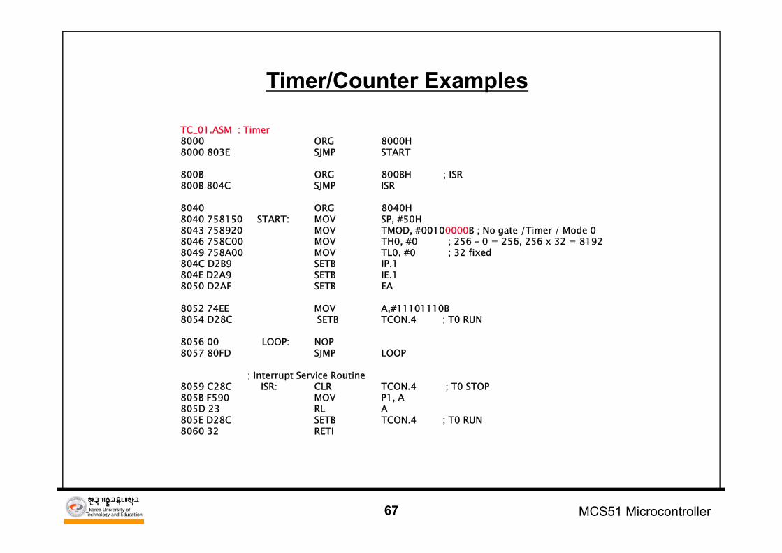
Timer/Counter Examples
TC_01.ASM : Timer8000 ORG 8000H8000 803E SJMP START
800B ORG 800BH ; ISR800B 804C SJMP ISR
8040 ORG 8040H8040 758150 START: MOV SP, #50H8043 758920 MOV TMOD, #00100000B ; No gate /Timer / Mode 08046 758C00 MOV TH0, #0 ; 256 – 0 = 256, 256 x 32 = 81928049 758A00 MOV TL0, #0 ; 32 fixed804C D2B9 SETB IP.1804E D2A9 SETB IE.18050 D2AF SETB EA
8052 74EE MOV A,#11101110B8054 D28C SETB TCON.4 ; T0 RUN
8056 00 LOOP: NOP8057 80FD SJMP LOOP
; Interrupt Service Routine8059 C28C ISR: CLR TCON.4 ; T0 STOP805B F590 MOV P1, A805D 23 RL A805E D28C SETB TCON.4 ; T0 RUN8060 32 RETI
68 MCS51 Microcontroller
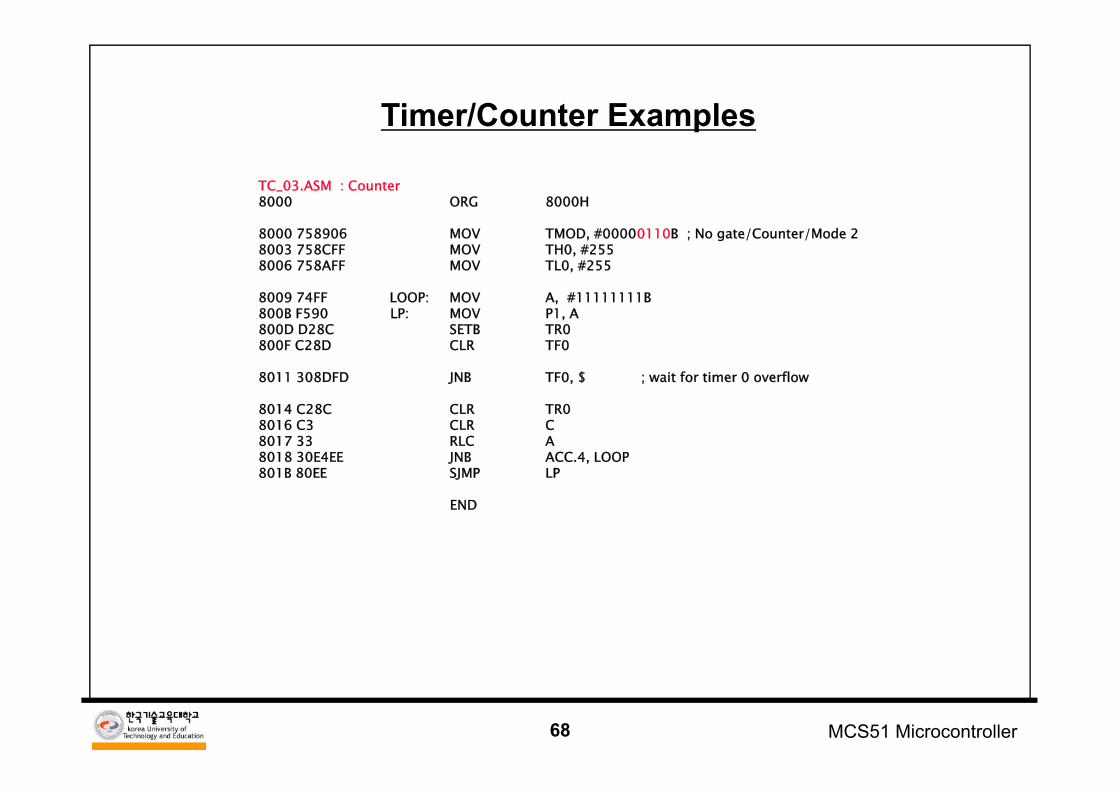
Timer/Counter Examples
TC_03.ASM : Counter8000 ORG 8000H
8000 758906 MOV TMOD, #00000110B ; No gate/Counter/Mode 28003 758CFF MOV TH0, #2558006 758AFF MOV TL0, #255
8009 74FF LOOP: MOV A, #11111111B800B F590 LP: MOV P1, A800D D28C SETB TR0800F C28D CLR TF0
8011 308DFD JNB TF0, $ ; wait for timer 0 overflow
8014 C28C CLR TR08016 C3 CLR C8017 33 RLC A8018 30E4EE JNB ACC.4, LOOP801B 80EE SJMP LP
END
69 MCS51 Microcontroller
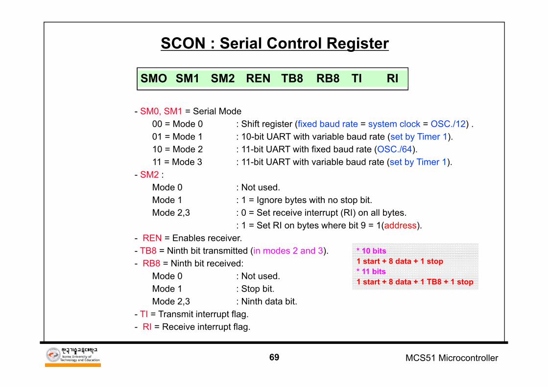
SCON : Serial Control Register
- SM0, SM1 = Serial Mode00 = Mode 0 : Shift register (fixed baud rate = system clock = OSC./12) .01 = Mode 1 : 10-bit UART with variable baud rate (set by Timer 1).10 = Mode 2 : 11-bit UART with fixed baud rate (OSC./64).11 = Mode 3 : 11-bit UART with variable baud rate (set by Timer 1).
- SM2 :Mode 0 : Not used.Mode 1 : 1 = Ignore bytes with no stop bit.Mode 2,3 : 0 = Set receive interrupt (RI) on all bytes.
: 1 = Set RI on bytes where bit 9 = 1(address).- REN = Enables receiver.- TB8 = Ninth bit transmitted (in modes 2 and 3).- RB8 = Ninth bit received:
Mode 0 : Not used.Mode 1 : Stop bit.Mode 2,3 : Ninth data bit.
- TI = Transmit interrupt flag.- RI = Receive interrupt flag.
SMO SM1 SM2 REN TB8 RB8 TI RI
* 10 bits1 start + 8 data + 1 stop* 11 bits1 start + 8 data + 1 TB8 + 1 stop
70 MCS51 Microcontroller
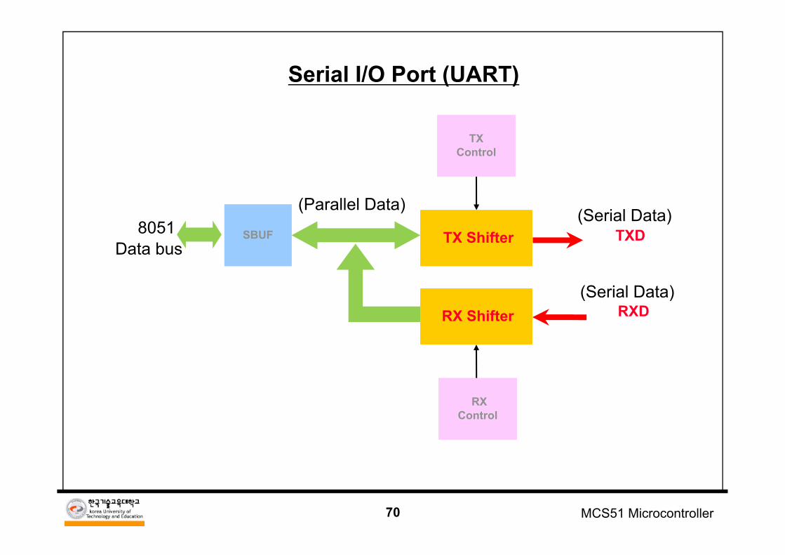
Serial I/O Port (UART)
SBUFSBUF TX ShifterTX Shifter
RXControl
RXControl
RX ShifterRX Shifter
TX Control
TX Control
8051Data bus
(Parallel Data) (Serial Data)TXD
(Serial Data)RXD
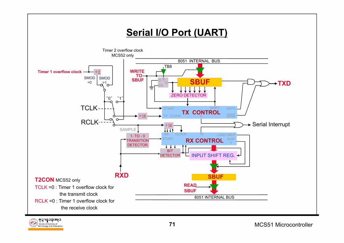
71 MCS51 Microcontroller
Serial I/O Port (UART)
÷16
BITDETECTOR
“1”
TCLK
8051 INTERNAL BUS
8051 INTERNAL BUS
S
CK SBUFZERO DETECTOR
START
TX CLOCK
DATA
SENDTITX CONTROL
START RX CONTROL
SBUFREADSBUF
WRITETO
SBUF
TB8
TXD
SHIFT
Serial InterruptRX CLOCK RI
SAMPLE1- TO - 0
TRANSITIONDETECTOR
RCLK
RXD
“0”
Timer 2 overflow clockMCS52 only
÷2÷2
SMOD=1
SMOD=0
Timer 1 overflow clock
LOAD SBUFSHIF
T
÷16
INPUT SHIFT REG.INPUT SHIFT REG.
DQ
T2CON MCS52 onlyTCLK =0 : Timer 1 overflow clock for
the transmit clockRCLK =0 : Timer 1 overflow clock for
the receive clock
72 MCS51 Microcontroller
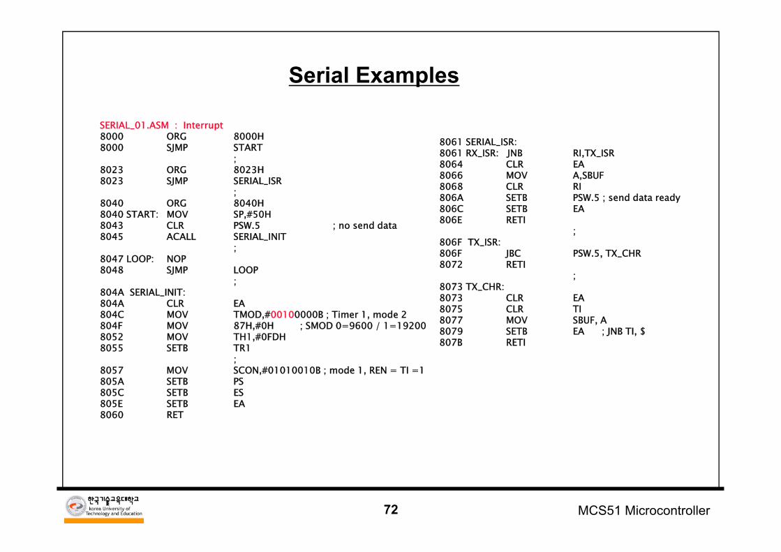
Serial Examples
SERIAL_01.ASM : Interrupt8000 ORG 8000H8000 SJMP START
;8023 ORG 8023H8023 SJMP SERIAL_ISR
;8040 ORG 8040H8040 START: MOV SP,#50H8043 CLR PSW.5 ; no send data8045 ACALL SERIAL_INIT
;8047 LOOP: NOP8048 SJMP LOOP
;804A SERIAL_INIT:804A CLR EA804C MOV TMOD,#00100000B ; Timer 1, mode 2804F MOV 87H,#0H ; SMOD 0=9600 / 1=192008052 MOV TH1,#0FDH8055 SETB TR1
;8057 MOV SCON,#01010010B ; mode 1, REN = TI =1805A SETB PS805C SETB ES805E SETB EA8060 RET
8061 SERIAL_ISR:8061 RX_ISR: JNB RI,TX_ISR8064 CLR EA8066 MOV A,SBUF8068 CLR RI806A SETB PSW.5 ; send data ready806C SETB EA806E RETI
;806F TX_ISR:806F JBC PSW.5, TX_CHR8072 RETI
;8073 TX_CHR:8073 CLR EA8075 CLR TI8077 MOV SBUF, A8079 SETB EA ; JNB TI, $807B RETI
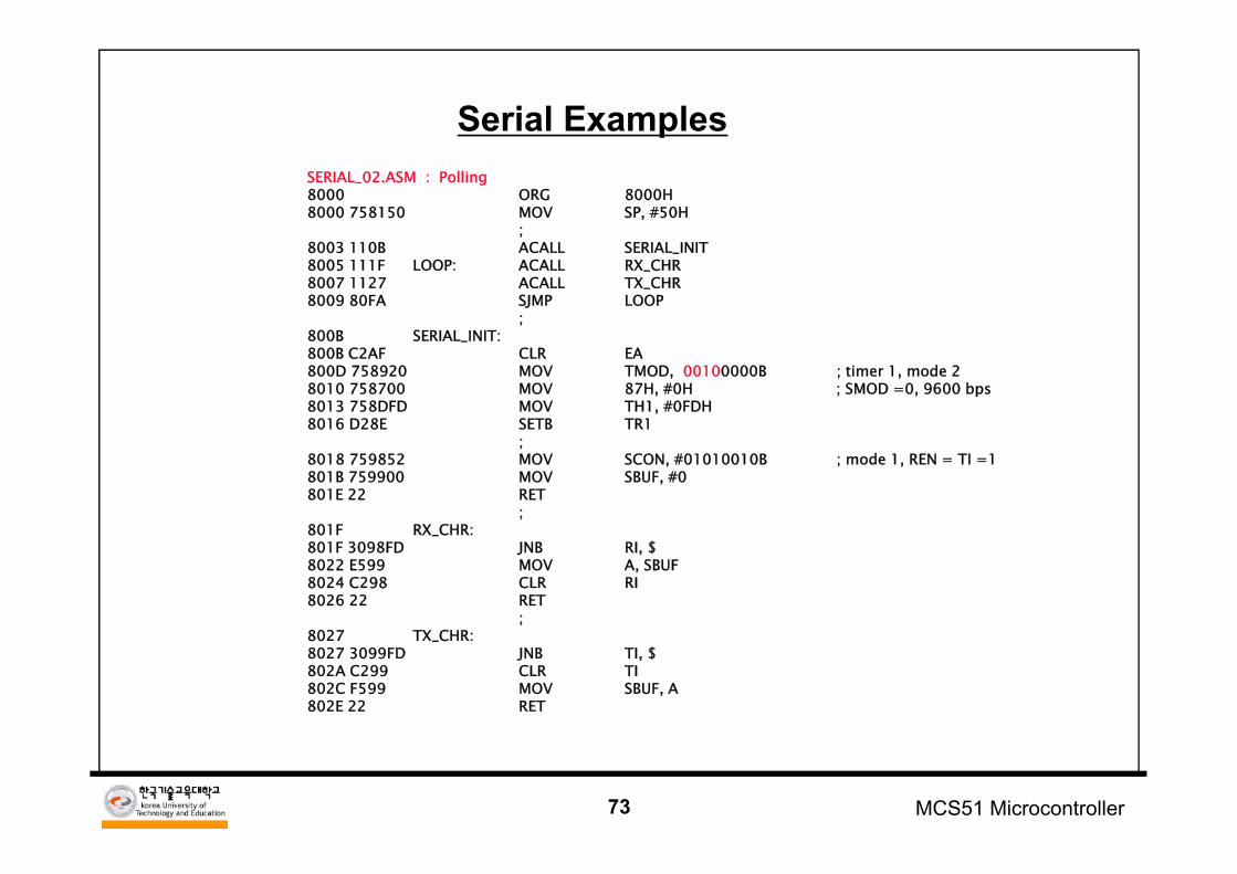
73 MCS51 Microcontroller
Serial ExamplesSERIAL_02.ASM : Polling8000 ORG 8000H8000 758150 MOV SP, #50H
;8003 110B ACALL SERIAL_INIT8005 111F LOOP: ACALL RX_CHR8007 1127 ACALL TX_CHR8009 80FA SJMP LOOP
;800B SERIAL_INIT:800B C2AF CLR EA800D 758920 MOV TMOD, 00100000B ; timer 1, mode 28010 758700 MOV 87H, #0H ; SMOD =0, 9600 bps8013 758DFD MOV TH1, #0FDH8016 D28E SETB TR1
;8018 759852 MOV SCON, #01010010B ; mode 1, REN = TI =1801B 759900 MOV SBUF, #0801E 22 RET
;801F RX_CHR:801F 3098FD JNB RI, $8022 E599 MOV A, SBUF8024 C298 CLR RI8026 22 RET
;8027 TX_CHR:8027 3099FD JNB TI, $802A C299 CLR TI802C F599 MOV SBUF, A802E 22 RET
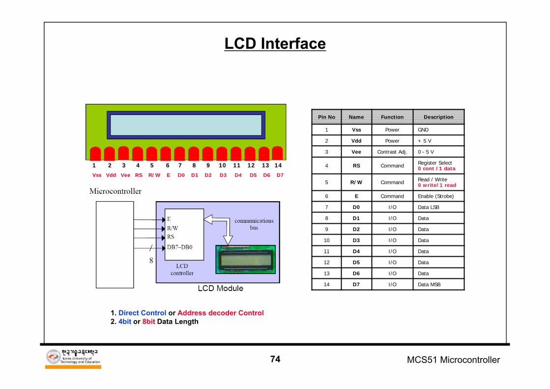
74 MCS51 Microcontroller
Pin No Name Function Description
1 Vss Power GND
2 Vdd Power + 5 V
3 Vee Contrast Adj. 0 - 5 V
4 RS Command Register Select0 cont /1 data
5 R/W Command Read / Write0 write/1 read
6 E Command Enable (Strobe)
7 D0 I/O Data LSB
8 D1 I/O Data
9 D2 I/O Data
10 D3 I/O Data
11 D4 I/O Data
12 D5 I/O Data
13 D6 I/O Data
14 D7 I/O Data MSB
1 2 3 4 5 6 7 8 9 10 11 12 13 14
Vss Vdd Vee RS R/W E D0 D1 D2 D3 D4 D5 D6 D7
1. Direct Control or Address decoder Control2. 4bit or 8bit Data Length
LCD Interface
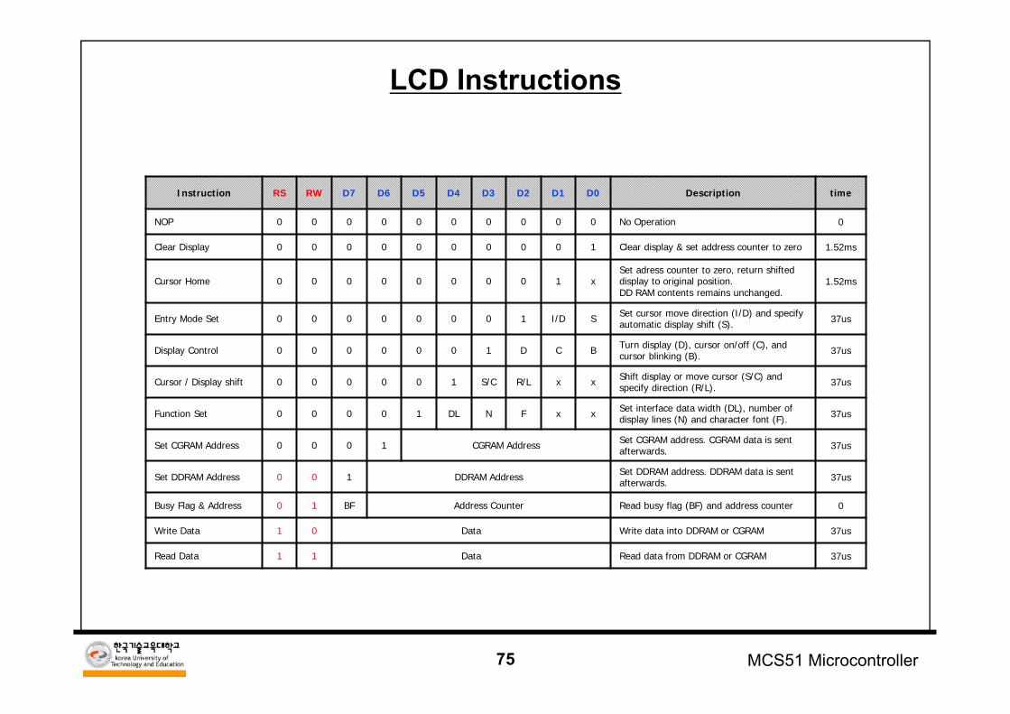
75 MCS51 Microcontroller
Instruction RS RW D7 D6 D5 D4 D3 D2 D1 D0 Description time
NOP 0 0 0 0 0 0 0 0 0 0 No Operation 0
Clear Display 0 0 0 0 0 0 0 0 0 1 Clear display & set address counter to zero 1.52ms
Cursor Home 0 0 0 0 0 0 0 0 1 xSet adress counter to zero, return shifted display to original position.DD RAM contents remains unchanged.
1.52ms
Entry Mode Set 0 0 0 0 0 0 0 1 I/D S Set cursor move direction (I/D) and specify automatic display shift (S). 37us
Display Control 0 0 0 0 0 0 1 D C B Turn display (D), cursor on/off (C), and cursor blinking (B). 37us
Cursor / Display shift 0 0 0 0 0 1 S/C R/L x x Shift display or move cursor (S/C) and specify direction (R/L). 37us
Function Set 0 0 0 0 1 DL N F x x Set interface data width (DL), number of display lines (N) and character font (F). 37us
Set CGRAM Address 0 0 0 1 CGRAM Address Set CGRAM address. CGRAM data is sent afterwards. 37us
Set DDRAM Address 0 0 1 DDRAM Address Set DDRAM address. DDRAM data is sent afterwards. 37us
Busy Flag & Address 0 1 BF Address Counter Read busy flag (BF) and address counter 0
Write Data 1 0 Data Write data into DDRAM or CGRAM 37us
Read Data 1 1 Data Read data from DDRAM or CGRAM 37us
LCD Instructions
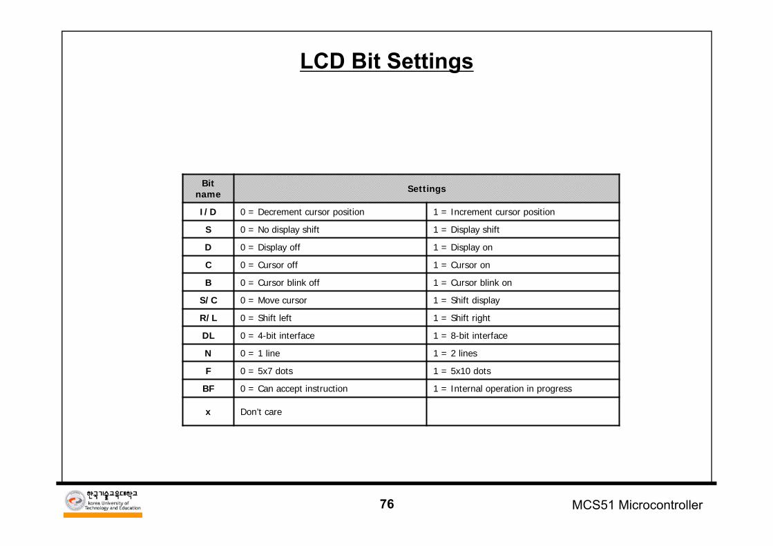
76 MCS51 Microcontroller
Bit name Settings
I/D 0 = Decrement cursor position 1 = Increment cursor position
S 0 = No display shift 1 = Display shift
D 0 = Display off 1 = Display on
C 0 = Cursor off 1 = Cursor on
B 0 = Cursor blink off 1 = Cursor blink on
S/C 0 = Move cursor 1 = Shift display
R/L 0 = Shift left 1 = Shift right
DL 0 = 4-bit interface 1 = 8-bit interface
N 0 = 1 line 1 = 2 lines
F 0 = 5x7 dots 1 = 5x10 dots
BF 0 = Can accept instruction 1 = Internal operation in progress
x Don’t care DDRAM : Display Data RAMCGRAM : Character Generator RAM
LCD Bit Settings
77 MCS51 Microcontroller
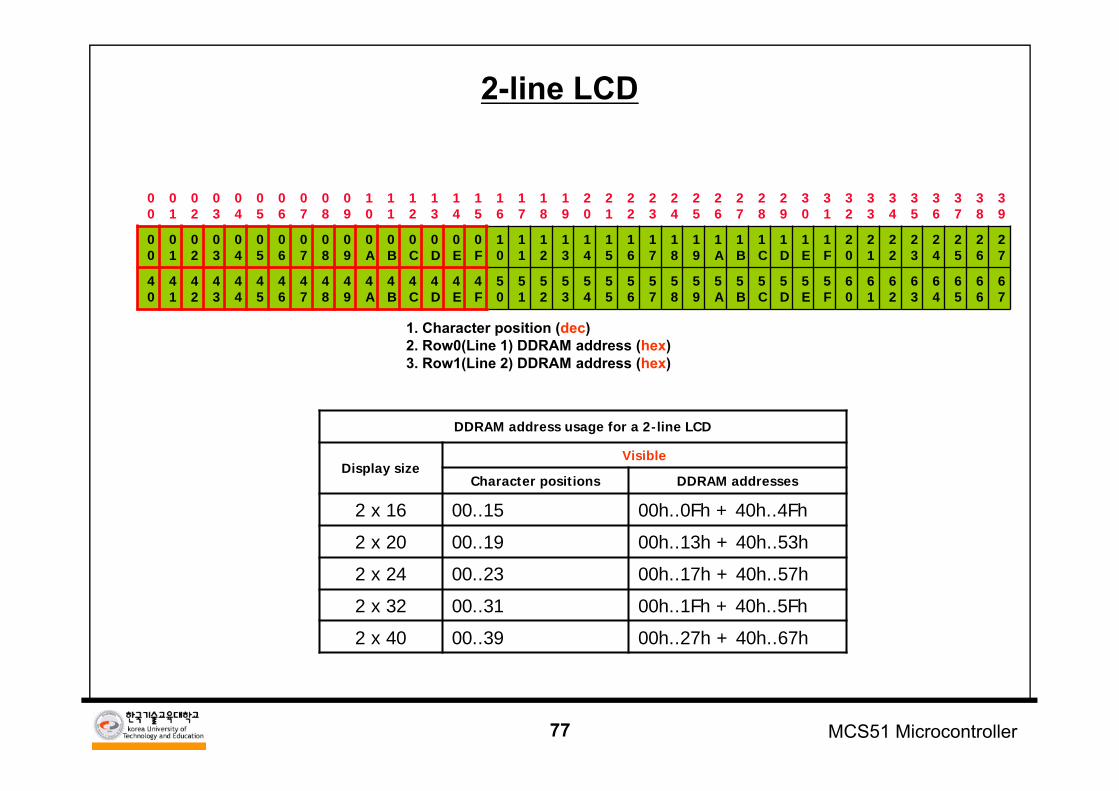
DDRAM address usage for a 2-line LCD
Display sizeVisible
Character positions DDRAM addresses
2 x 16 00..15 00h..0Fh + 40h..4Fh
2 x 20 00..19 00h..13h + 40h..53h
2 x 24 00..23 00h..17h + 40h..57h
2 x 32 00..31 00h..1Fh + 40h..5Fh
2 x 40 00..39 00h..27h + 40h..67h
1. Character position (dec)2. Row0(Line 1) DDRAM address (hex)3. Row1(Line 2) DDRAM address (hex)
00
01
02
03
04
05
06
07
08
09
10
11
12
13
14
15
16
17
18
19
20
21
22
23
24
25
26
27
28
29
30
31
32
33
34
35
36
37
38
39
00
01
02
03
04
05
06
07
08
09
0A
0B
0C
0D
0E
0F
10
11
12
13
14
15
16
17
18
19
1A
1B
1C
1D
1E
1F
20
21
22
23
24
25
26
27
40
41
42
43
44
45
46
47
48
49
4A
4B
4C
4D
4E
4F
50
51
52
53
54
55
56
57
58
59
5A
5B
5C
5D
5E
5F
60
61
62
63
64
65
66
67
2-line LCD
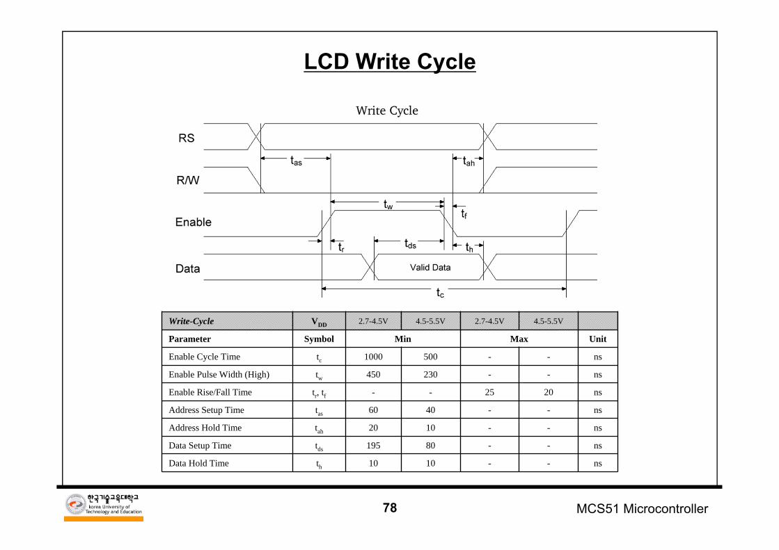
78 MCS51 Microcontroller
Write-Cycle VDD 2.7-4.5V 4.5-5.5V 2.7-4.5V 4.5-5.5V
Parameter Symbol Min Max Unit
Enable Cycle Time tc 1000 500 - - ns
Enable Pulse Width (High) tw 450 230 - - ns
Enable Rise/Fall Time tr, tf - - 25 20 ns
Address Setup Time tas 60 40 - - ns
Address Hold Time tah 20 10 - - ns
Data Setup Time tds 195 80 - - ns
Data Hold Time th 10 10 - - ns
LCD Write Cycle
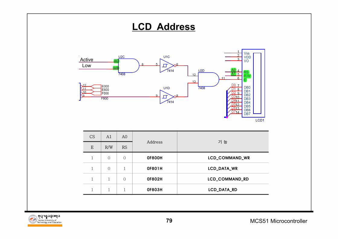
79 MCS51 Microcontroller
LCD Address
CS A1 A0
Address 기 능
E R/W RS
1 0 0 0F800H LCD_COMMAND_WR
1 0 1 0F801H LCD_DATA_WR
1 1 0 0F802H LCD_COMMAND_RD
1 1 1 0F803H LCD_DATA_RD
Active Low
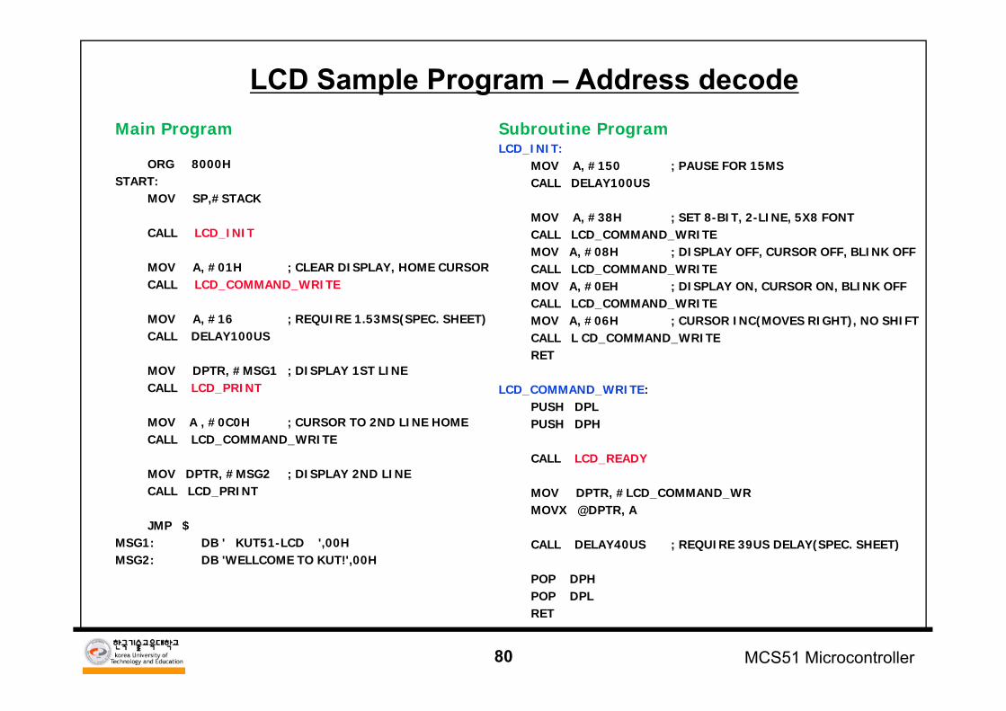
80 MCS51 Microcontroller
Main Program
ORG 8000HSTART:
MOV SP,#STACK
CALL LCD_INIT
MOV A, #01H ; CLEAR DISPLAY, HOME CURSORCALL LCD_COMMAND_WRITE
MOV A, #16 ; REQUIRE 1.53MS(SPEC. SHEET)CALL DELAY100US
MOV DPTR, #MSG1 ; DISPLAY 1ST LINECALL LCD_PRINT
MOV A , #0C0H ; CURSOR TO 2ND LINE HOMECALL LCD_COMMAND_WRITE
MOV DPTR, #MSG2 ; DISPLAY 2ND LINECALL LCD_PRINT
JMP $MSG1: DB ' KUT51-LCD ',00HMSG2: DB 'WELLCOME TO KUT!',00H
Subroutine ProgramLCD_INIT:
MOV A, #150 ; PAUSE FOR 15MSCALL DELAY100US
MOV A, #38H ; SET 8-BIT, 2-LINE, 5X8 FONTCALL LCD_COMMAND_WRITEMOV A, #08H ; DISPLAY OFF, CURSOR OFF, BLINK OFFCALL LCD_COMMAND_WRITEMOV A, #0EH ; DISPLAY ON, CURSOR ON, BLINK OFFCALL LCD_COMMAND_WRITEMOV A, #06H ; CURSOR INC(MOVES RIGHT), NO SHIFTCALL L CD_COMMAND_WRITERET
LCD_COMMAND_WRITE:PUSH DPLPUSH DPH
CALL LCD_READY
MOV DPTR, #LCD_COMMAND_WRMOVX @DPTR, A
CALL DELAY40US ; REQUIRE 39US DELAY(SPEC. SHEET)
POP DPHPOP DPLRET
LCD Sample Program – Address decode
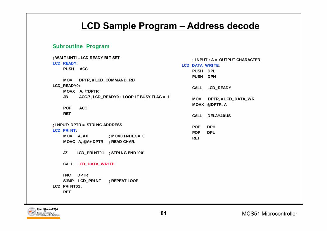
81 MCS51 Microcontroller
Subroutine Program
; WAIT UNTIL LCD READY BIT SETLCD_READY:
PUSH ACC
MOV DPTR, #LCD_COMMAND_RDLCD_READY0:
MOVX A, @DPTRJB ACC.7, LCD_READY0 ; LOOP IF BUSY FLAG = 1
POP ACCRET
; INPUT: DPTR = STRING ADDRESS LCD_PRINT:
MOV A, #0 ; MOVC INDEX = 0MOVC A, @A+DPTR ; READ CHAR.
JZ LCD_PRINT01 ; STRING END '00'
CALL LCD_DATA_WRITE
INC DPTRSJMP LCD_PRINT ; REPEAT LOOP
LCD_PRINT01:RET
; INPUT : A = OUTPUT CHARACTERLCD_DATA_WRITE:
PUSH DPLPUSH DPH
CALL LCD_READY
MOV DPTR, #LCD_DATA_WRMOVX @DPTR, A
CALL DELAY40US
POP DPHPOP DPLRET
LCD Sample Program – Address decode
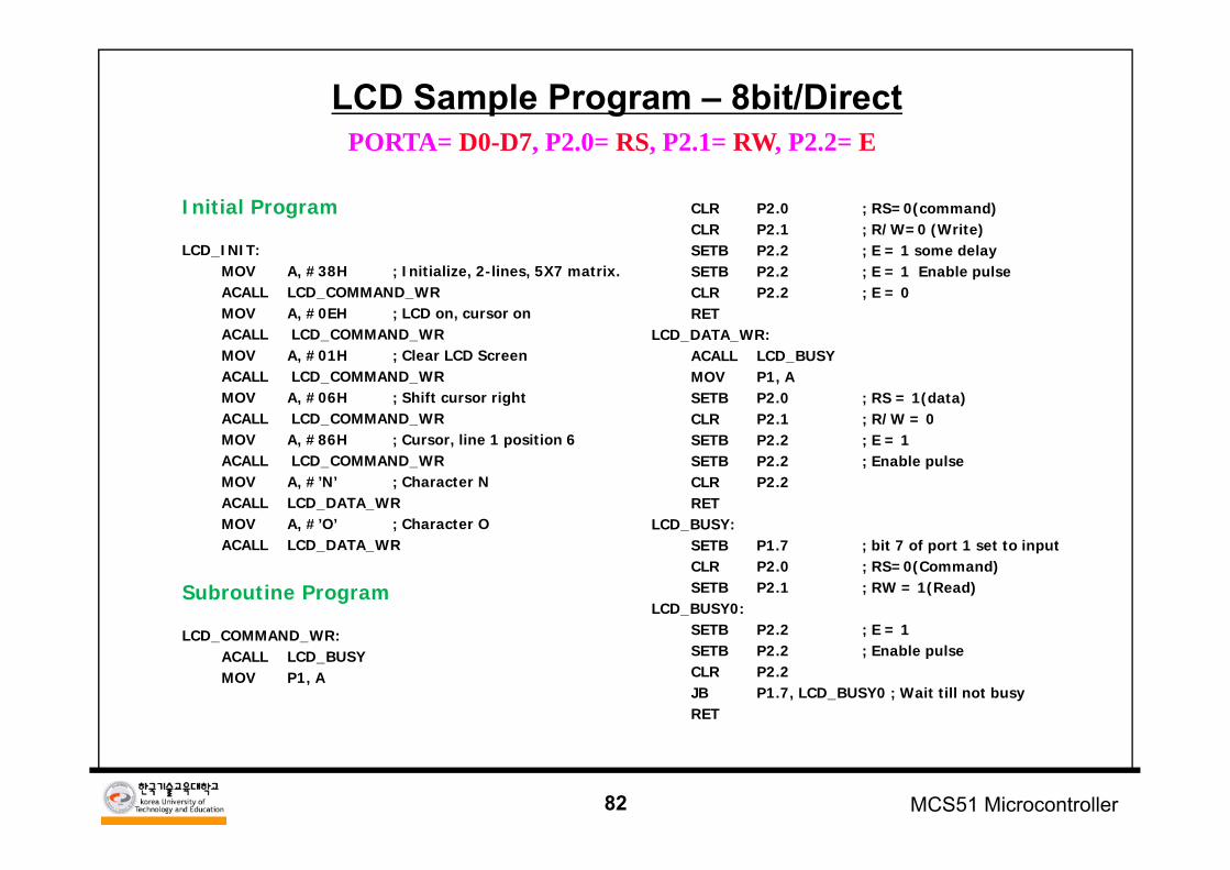
82 MCS51 Microcontroller
PORTA= D0-D7, P2.0= RS, P2.1= RW, P2.2= ELCD Sample Program – 8bit/Direct
Initial Program
LCD_INIT:MOV A, #38H ; Initialize, 2-lines, 5X7 matrix.ACALL LCD_COMMAND_WRMOV A, #0EH ; LCD on, cursor onACALL LCD_COMMAND_WRMOV A, #01H ; Clear LCD ScreenACALL LCD_COMMAND_WRMOV A, #06H ; Shift cursor rightACALL LCD_COMMAND_WRMOV A, #86H ; Cursor, line 1 position 6ACALL LCD_COMMAND_WR MOV A, #’N’ ; Character NACALL LCD_DATA_WRMOV A, #’O’ ; Character OACALL LCD_DATA_WR
Subroutine Program
LCD_COMMAND_WR: ACALL LCD_BUSYMOV P1, A
CLR P2.0 ; RS=0(command)CLR P2.1 ; R/W=0 (Write)SETB P2.2 ; E = 1 some delaySETB P2.2 ; E = 1 Enable pulseCLR P2.2 ; E = 0 RET
LCD_DATA_WR: ACALL LCD_BUSYMOV P1, ASETB P2.0 ; RS = 1(data)CLR P2.1 ; R/W = 0SETB P2.2 ; E = 1SETB P2.2 ; Enable pulseCLR P2.2RET
LCD_BUSY:SETB P1.7 ; bit 7 of port 1 set to inputCLR P2.0 ; RS=0(Command)SETB P2.1 ; RW = 1(Read)
LCD_BUSY0:SETB P2.2 ; E = 1SETB P2.2 ; Enable pulseCLR P2.2JB P1.7, LCD_BUSY0 ; Wait till not busyRET
83 MCS51 Microcontroller
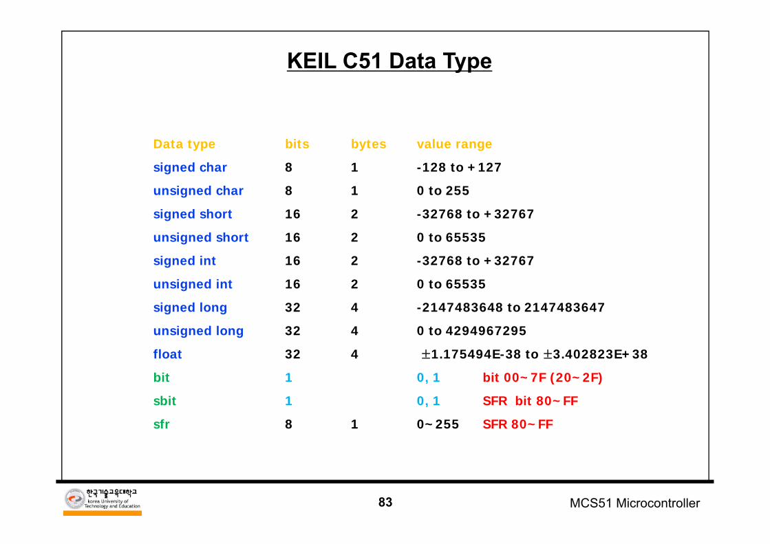
KEIL C51 Data Type
Data type bits bytes value range
signed char 8 1 -128 to +127
unsigned char 8 1 0 to 255
signed short 16 2 -32768 to +32767
unsigned short 16 2 0 to 65535
signed int 16 2 -32768 to +32767
unsigned int 16 2 0 to 65535
signed long 32 4 -2147483648 to 2147483647
unsigned long 32 4 0 to 4294967295
float 32 4 ±1.175494E-38 to ±3.402823E+38
bit 1 0, 1 bit 00~7F (20~2F)
sbit 1 0, 1 SFR bit 80~FF
sfr 8 1 0~255 SFR 80~FF
84 MCS51 Microcontroller
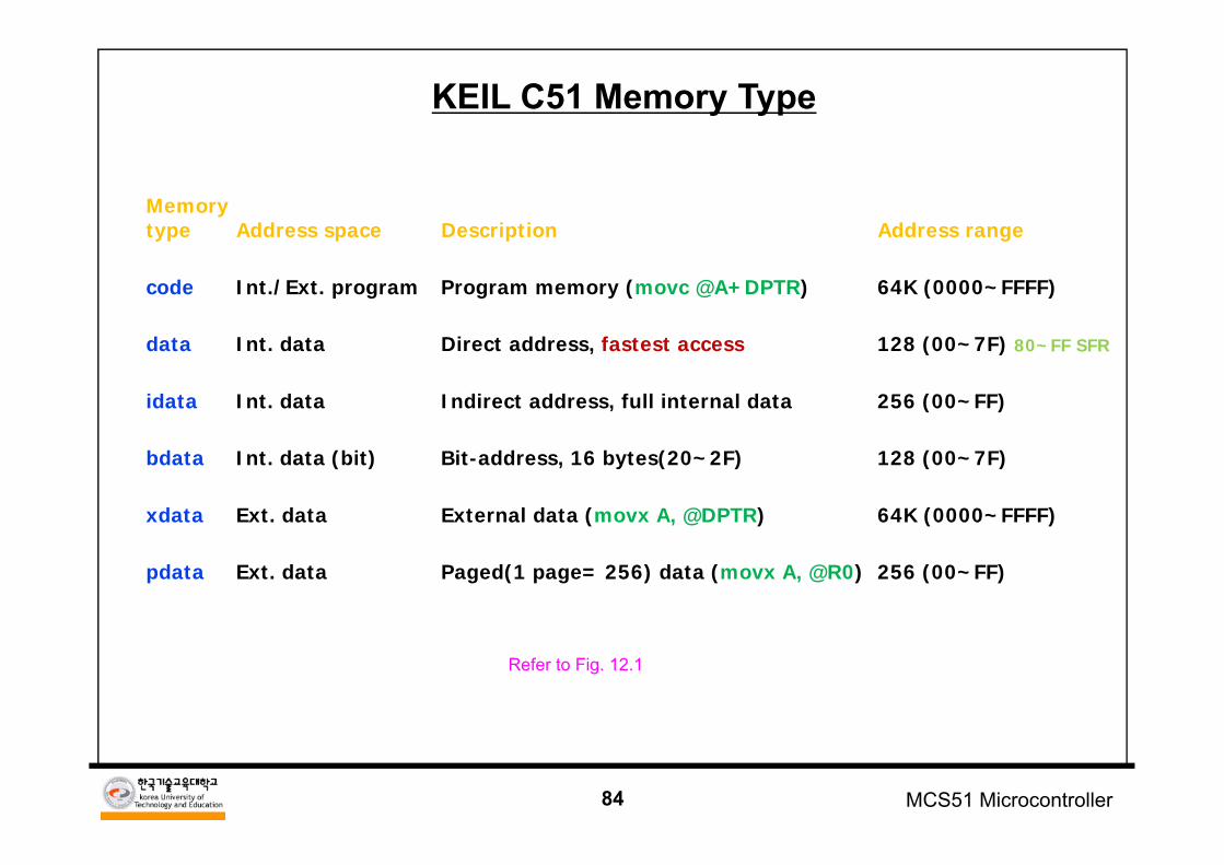
KEIL C51 Memory Type
Memory type Address space Description Address range
code Int./Ext. program Program memory (movc @A+DPTR) 64K (0000~FFFF)
data Int. data Direct address, fastest access 128 (00~7F) 80~FF SFR
idata Int. data Indirect address, full internal data 256 (00~FF)
bdata Int. data (bit) Bit-address, 16 bytes(20~2F) 128 (00~7F)
xdata Ext. data External data (movx A, @DPTR) 64K (0000~FFFF)
pdata Ext. data Paged(1 page= 256) data (movx A, @R0) 256 (00~FF)
Refer to Fig. 12.1
85 MCS51 Microcontroller
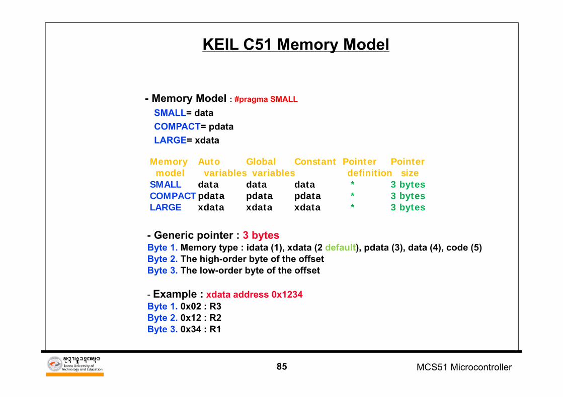
KEIL C51 Memory Model
- Memory Model : #pragma SMALL
SMALL= dataCOMPACT= pdata LARGE= xdata
Memory Auto Global Constant Pointer Pointermodel variables variables definition size
SMALL data data data * 3 bytes COMPACT pdata pdata pdata * 3 bytes LARGE xdata xdata xdata * 3 bytes
- Generic pointer : 3 bytesByte 1. Memory type : idata (1), xdata (2 default), pdata (3), data (4), code (5) Byte 2. The high-order byte of the offsetByte 3. The low-order byte of the offset
- Example : xdata address 0x1234Byte 1. 0x02 : R3Byte 2. 0x12 : R2Byte 3. 0x34 : R1
86 MCS51 Microcontroller
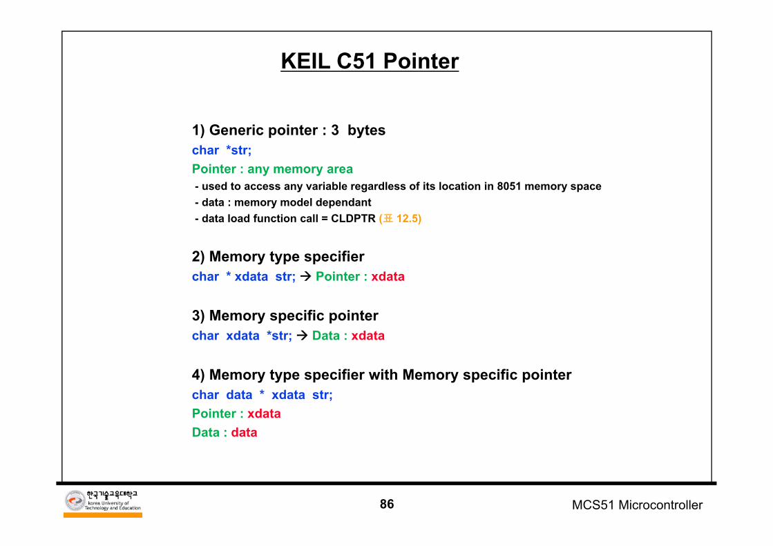
KEIL C51 Pointer
1) Generic pointer : 3 bytes char *str;Pointer : any memory area- used to access any variable regardless of its location in 8051 memory space- data : memory model dependant- data load function call = CLDPTR (표 12.5)
2) Memory type specifierchar * xdata str; Pointer : xdata
3) Memory specific pointerchar xdata *str; Data : xdata
4) Memory type specifier with Memory specific pointerchar data * xdata str;Pointer : xdataData : data
87 MCS51 Microcontroller
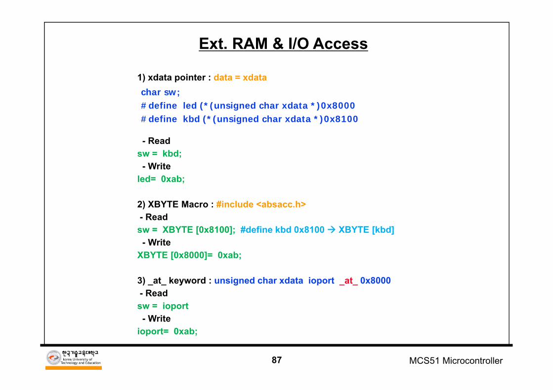
Ext. RAM & I/O Access
1) xdata pointer : data = xdata
- Readsw = kbd;- Write
led= 0xab;
2) XBYTE Macro : #include <absacc.h>- Read
sw = XBYTE [0x8100]; #define kbd 0x8100 XBYTE [kbd]- Write
XBYTE [0x8000]= 0xab;
3) _at_ keyword : unsigned char xdata ioport _at_ 0x8000- Read
sw = ioport- Write
ioport= 0xab;
char sw;#define led (*(unsigned char xdata *)0x8000#define kbd (*(unsigned char xdata *)0x8100
88 MCS51 Microcontroller
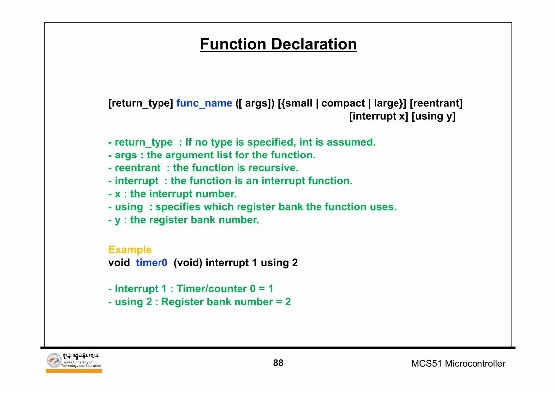
Function Declaration
[return_type] func_name ([ args]) [{small | compact | large}] [reentrant][interrupt x] [using y]
- return_type : If no type is specified, int is assumed. - args : the argument list for the function.- reentrant : the function is recursive. - interrupt : the function is an interrupt function. - x : the interrupt number. - using : specifies which register bank the function uses. - y : the register bank number.
Examplevoid timer0 (void) interrupt 1 using 2
- Interrupt 1 : Timer/counter 0 = 1- using 2 : Register bank number = 2
89 MCS51 Microcontroller
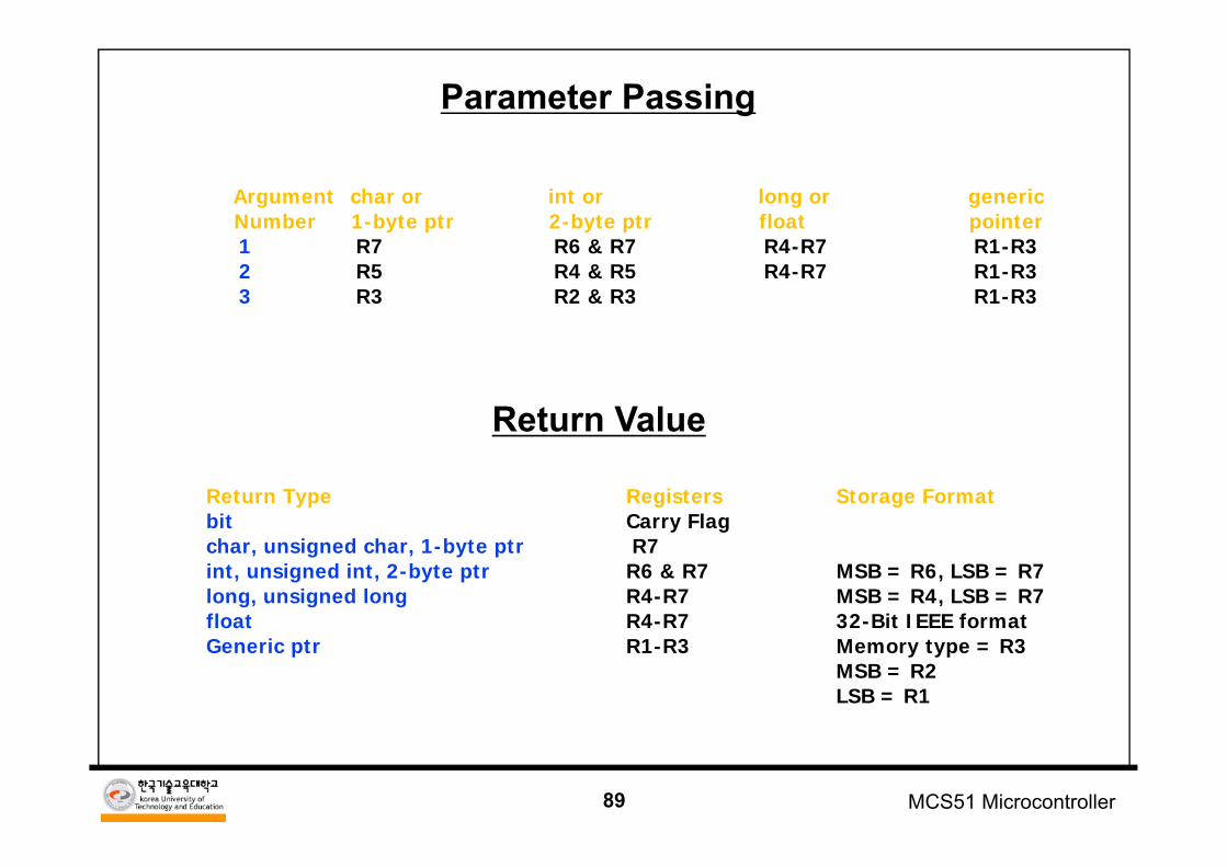
Parameter Passing
Argument char or int or long or genericNumber 1-byte ptr 2-byte ptr float pointer1 R7 R6 & R7 R4-R7 R1-R3 2 R5 R4 & R5 R4-R7 R1-R3 3 R3 R2 & R3 R1-R3
Return Value
Return Type Registers Storage Formatbit Carry Flag char, unsigned char, 1-byte ptr R7 int, unsigned int, 2-byte ptr R6 & R7 MSB = R6, LSB = R7 long, unsigned long R4-R7 MSB = R4, LSB = R7 float R4-R7 32-Bit IEEE format Generic ptr R1-R3 Memory type = R3
MSB = R2 LSB = R1
90 MCS51 Microcontroller
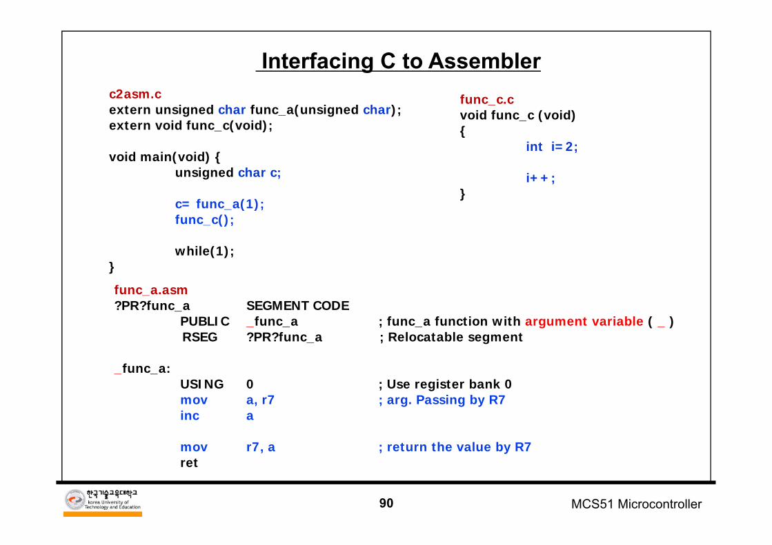
Interfacing C to Assemblerc2asm.cextern unsigned char func_a(unsigned char);extern void func_c(void);
void main(void) {unsigned char c;
c= func_a(1); func_c();
while(1);}
func_a.asm?PR?func_a SEGMENT CODE
PUBLIC _func_a ; func_a function with argument variable ( _ )RSEG ?PR?func_a ; Relocatable segment
_func_a:USING 0 ; Use register bank 0mov a, r7 ; arg. Passing by R7inc a
mov r7, a ; return the value by R7ret
func_c.cvoid func_c (void){
int i=2;
i++;}
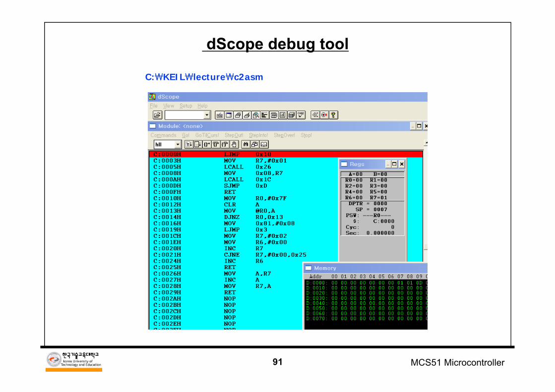
91 MCS51 Microcontroller
dScope debug tool
C:₩KEIL₩lecture₩c2asm
92 MCS51 Microcontroller
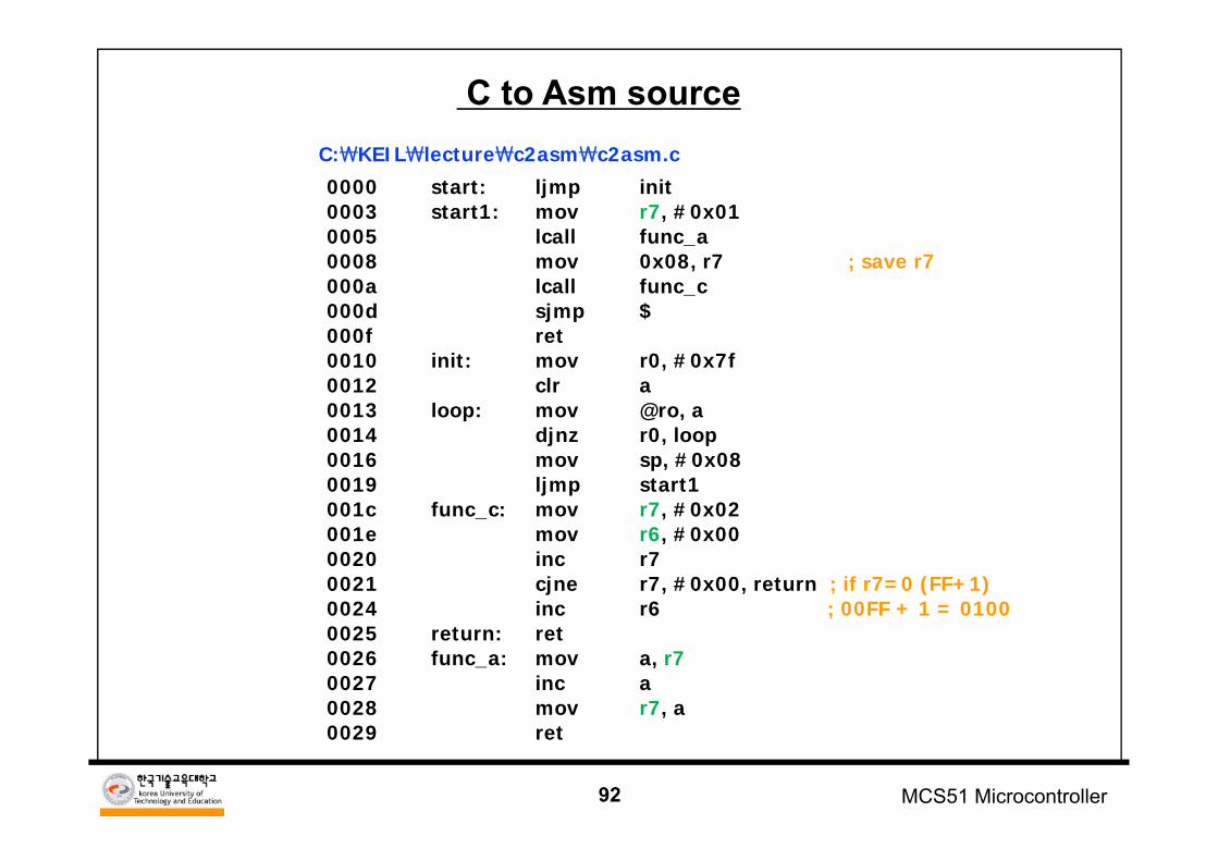
C to Asm sourceC:₩KEIL₩lecture₩c2asm₩c2asm.c
0000 start: ljmp init0003 start1: mov r7, #0x010005 lcall func_a0008 mov 0x08, r7 ; save r7000a lcall func_c000d sjmp $000f ret0010 init: mov r0, #0x7f0012 clr a0013 loop: mov @ro, a0014 djnz r0, loop0016 mov sp, #0x080019 ljmp start1001c func_c: mov r7, #0x02001e mov r6, #0x000020 inc r70021 cjne r7, #0x00, return ; if r7=0 (FF+1)0024 inc r6 ; 00FF + 1 = 01000025 return: ret0026 func_a: mov a, r70027 inc a 0028 mov r7, a0029 ret
93 MCS51 Microcontroller
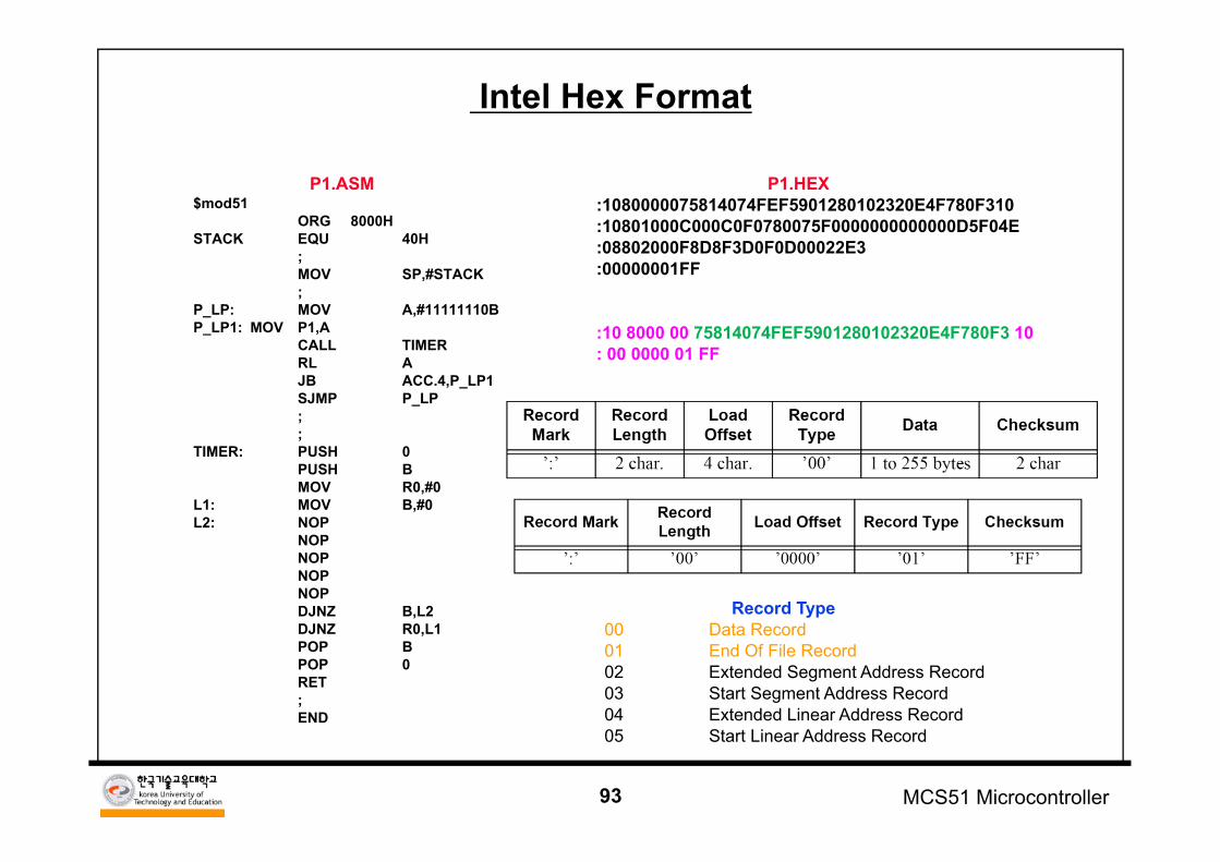
P1.ASM$mod51
ORG 8000HSTACK EQU 40H
;MOV SP,#STACK;
P_LP: MOV A,#11111110BP_LP1: MOV P1,A
CALL TIMERRL AJB ACC.4,P_LP1SJMP P_LP;;
TIMER: PUSH 0PUSH BMOV R0,#0
L1: MOV B,#0L2: NOP
NOPNOPNOPNOPDJNZ B,L2DJNZ R0,L1POP BPOP 0RET;END
P1.HEX:1080000075814074FEF5901280102320E4F780F310:10801000C000C0F0780075F0000000000000D5F04E:08802000F8D8F3D0F0D00022E3:00000001FF
:10 8000 00 75814074FEF5901280102320E4F780F3 10: 00 0000 01 FF
Intel Hex Format
Record Type00 Data Record01 End Of File Record02 Extended Segment Address Record 03 Start Segment Address Record 04 Extended Linear Address Record 05 Start Linear Address Record
94 MCS51 Microcontroller
1. LED Test Program
2. Digital I/O Test Program
3. External Interrupt Test Program
4. Timer Overflow Interrupt Test Program
5. Counter Test Program
6. RS-232 Serial Test Program
7. LCD Test Program
Test Program List
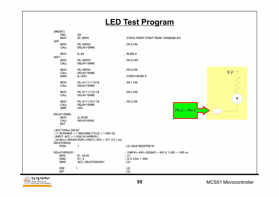
95 MCS51 Microcontroller
$MOD51ORG 0H MOV SP, #0FH ; STACK POINT START FROM 10H(BANK #2)
LED: MOV P0, #0FEH ; P0.0 ONCALL DELAY100MS
MOV B, #4 ; BLINK #LED1:
MOV P0, #0FFH ; P0.0 OFFCALL DELAY100MS
MOV P0, #0FEH ; P0.0 ONCALL DELAY100MSDJNZ B, LED1 ; CHECK BLINK #
MOV P0, #11111101B ; P0.1 ONCALL DELAY100MS
MOV P0, #11111011B ; P0.2 ONCALL DELAY100MS
MOV P0, #11110111B ; P0.3 ONCALL DELAY100MSSJMP LED
DELAY100MS:MOV A, #200CALL DELAY500USRET
; ACC*500us DELAY ; 11.0592MHZ = 1 MACHINE CYCLE = 1.085 US; INPUT: ACC = ? (500 US APPROX.); 2(CALL)+4(PUSH/POP)+2(RET)+463 = 471 (511 us)DELAY500US:
PUSH 1 ; (2) SAVE REGISTER R1
DELAY500US01: ; 1(MOV)+460+2(DJNZ) = 463 X 1.085 = 500 usMOV R1, #230 ; (1) DJNZ R1, $ ; (2 X 230) = 460DJNZ ACC, DELAY500US01 ; (2)
POP 1 ; (2)RET ; (2)
P0.0 – P0.3
5 V
LED Test Program
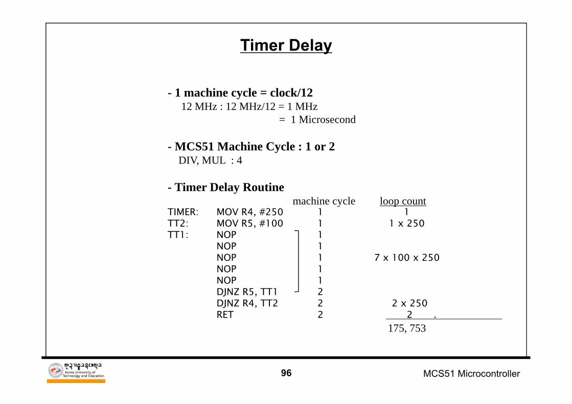
96 MCS51 Microcontroller
- 1 machine cycle = clock/1212 MHz : 12 MHz/12 = 1 MHz
= 1 Microsecond
- MCS51 Machine Cycle : 1 or 2 DIV, MUL : 4
- Timer Delay Routinemachine cycle loop count
TIMER: MOV R4, #250 1 1TT2: MOV R5, #100 1 1 x 250TT1: NOP 1
NOP 1NOP 1 7 x 100 x 250NOP 1NOP 1DJNZ R5, TT1 2DJNZ R4, TT2 2 2 x 250RET 2 2 .
175, 753
Timer Delay
97 MCS51 Microcontroller
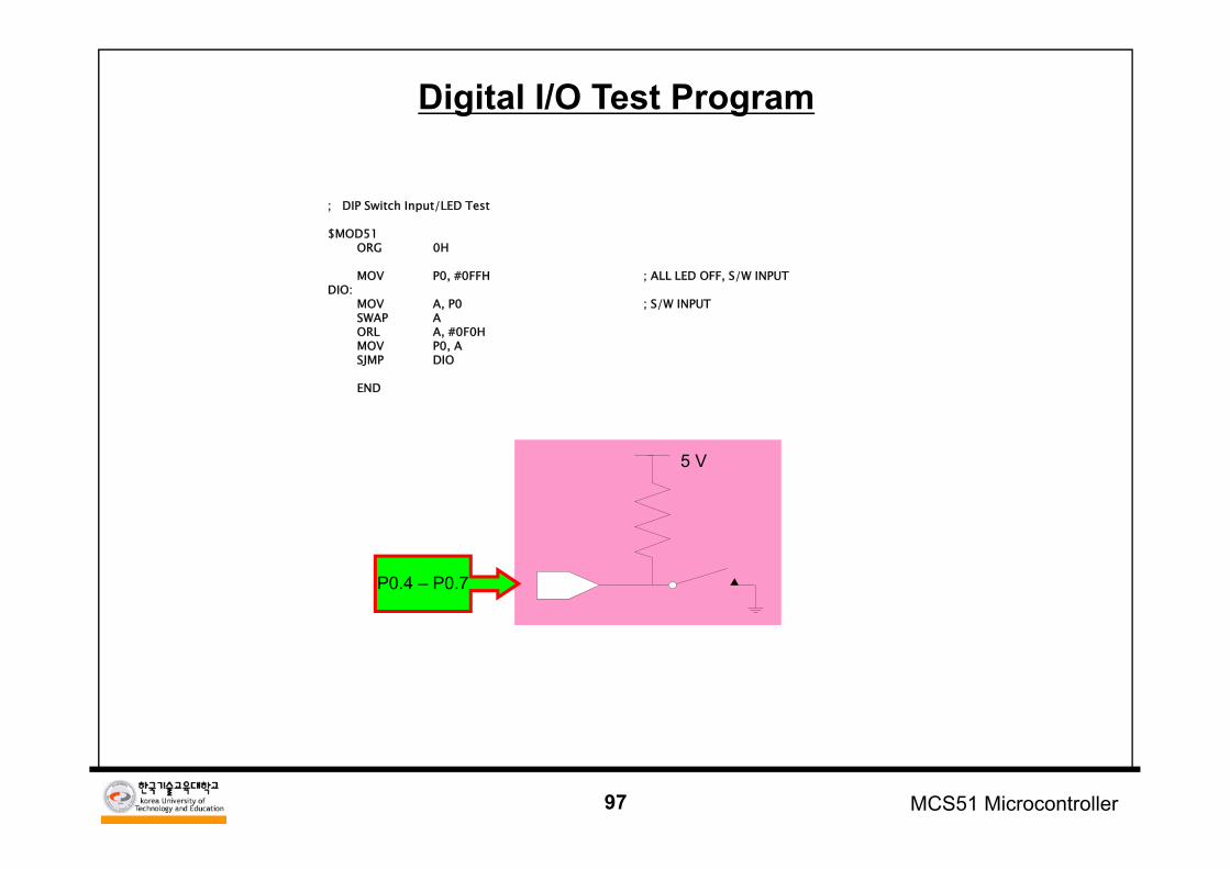
; DIP Switch Input/LED Test
$MOD51 ORG 0H
MOV P0, #0FFH ; ALL LED OFF, S/W INPUTDIO:
MOV A, P0 ; S/W INPUTSWAP AORL A, #0F0HMOV P0, ASJMP DIO
END
P0.4 – P0.7
5 V
Digital I/O Test Program
98 MCS51 Microcontroller
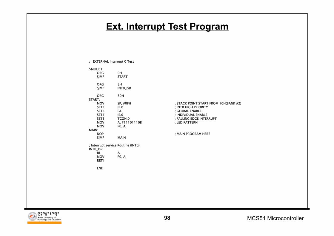
; EXTERNAL Interrupt 0 Test
$MOD51ORG 0HSJMP START
ORG 3HSJMP INT0_ISR
ORG 30HSTART:
MOV SP, #0FH ; STACK POINT START FROM 10H(BANK #2)SETB IP.0 ; INT0 HIGH PRIORITYSETB EA ; GLOBAL ENABLESETB IE.0 ; INDIVIDUAL ENABLESETB TCON.0 ; FALLING EDGE INTERRUPTMOV A, #11101110B ; LED PATTERNMOV P0, A
MAIN: NOP ; MAIN PROGRAM HERESJMP MAIN
; Interrupt Service Routine (INT0)INT0_ISR:
RL AMOV P0, ARETI
END
Ext. Interrupt Test Program
99 MCS51 Microcontroller
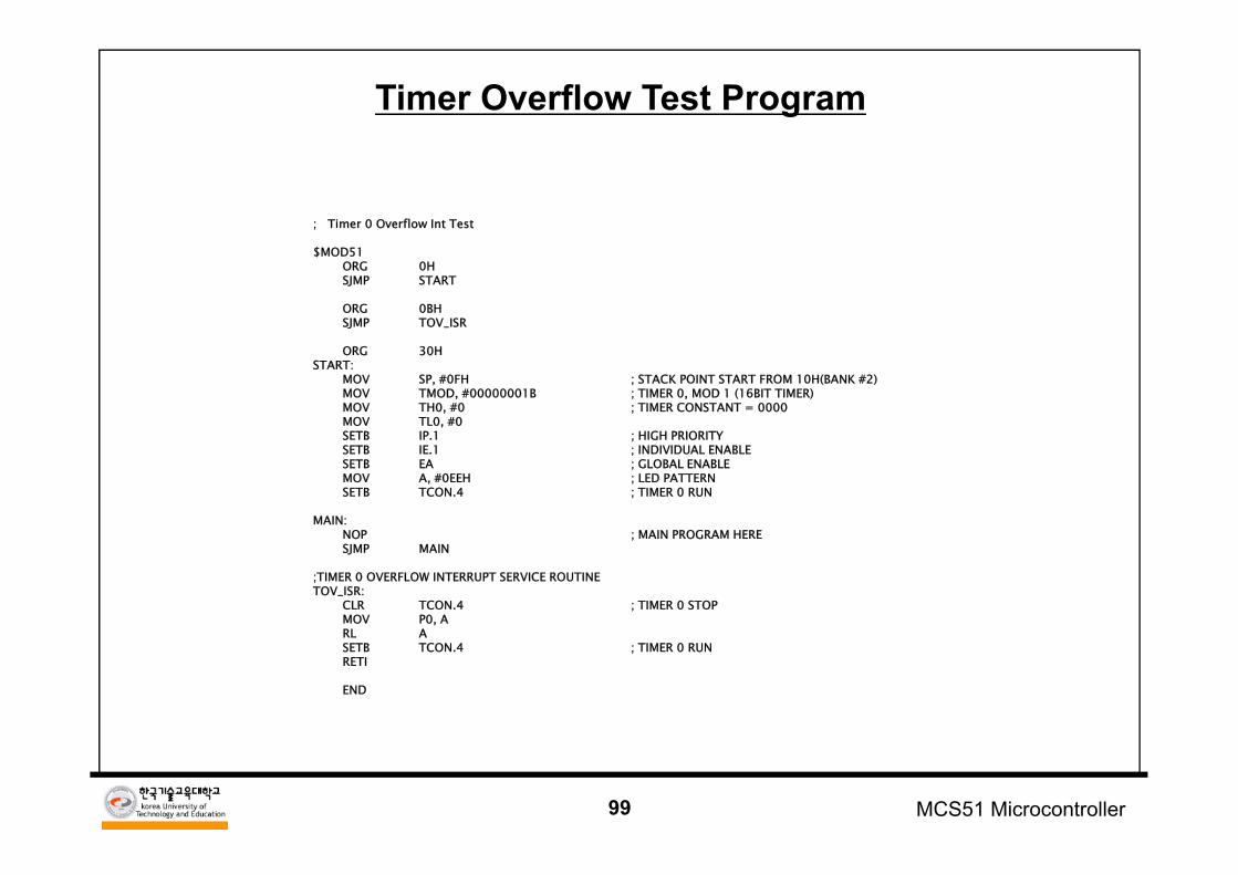
; Timer 0 Overflow Int Test
$MOD51ORG 0HSJMP START
ORG 0BHSJMP TOV_ISR
ORG 30HSTART:
MOV SP, #0FH ; STACK POINT START FROM 10H(BANK #2)MOV TMOD, #00000001B ; TIMER 0, MOD 1 (16BIT TIMER)MOV TH0, #0 ; TIMER CONSTANT = 0000MOV TL0, #0SETB IP.1 ; HIGH PRIORITYSETB IE.1 ; INDIVIDUAL ENABLESETB EA ; GLOBAL ENABLEMOV A, #0EEH ; LED PATTERNSETB TCON.4 ; TIMER 0 RUN
MAIN:NOP ; MAIN PROGRAM HERESJMP MAIN
;TIMER 0 OVERFLOW INTERRUPT SERVICE ROUTINETOV_ISR:
CLR TCON.4 ; TIMER 0 STOPMOV P0, ARL ASETB TCON.4 ; TIMER 0 RUNRETI
END
Timer Overflow Test Program
100 MCS51 Microcontroller
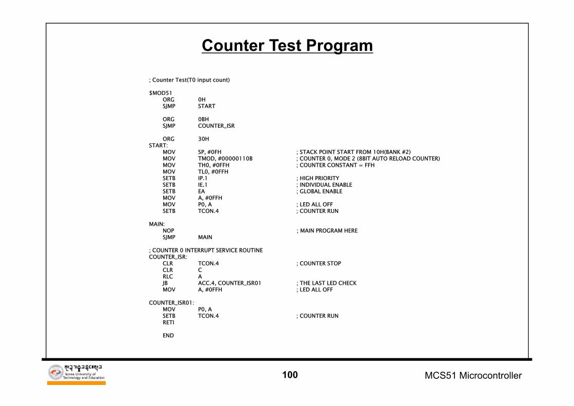
; Counter Test(T0 input count)
$MOD51ORG 0HSJMP START
ORG 0BHSJMP COUNTER_ISR
ORG 30HSTART:
MOV SP, #0FH ; STACK POINT START FROM 10H(BANK #2)MOV TMOD, #00000110B ; COUNTER 0, MODE 2 (8BIT AUTO RELOAD COUNTER)MOV TH0, #0FFH ; COUNTER CONSTANT = FFHMOV TL0, #0FFHSETB IP.1 ; HIGH PRIORITYSETB IE.1 ; INDIVIDUAL ENABLESETB EA ; GLOBAL ENABLEMOV A, #0FFH MOV P0, A ; LED ALL OFFSETB TCON.4 ; COUNTER RUN
MAIN:NOP ; MAIN PROGRAM HERESJMP MAIN
; COUNTER 0 INTERRUPT SERVICE ROUTINE COUNTER_ISR:
CLR TCON.4 ; COUNTER STOPCLR CRLC AJB ACC.4, COUNTER_ISR01 ; THE LAST LED CHECKMOV A, #0FFH ; LED ALL OFF
COUNTER_ISR01:MOV P0, ASETB TCON.4 ; COUNTER RUNRETI
END
Counter Test Program
101 MCS51 Microcontroller
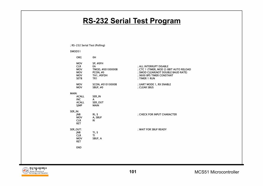
; RS-232 Serial Test (Polling)
$MOD51
ORG 0H
MOV SP, #0FHCLR EA ; ALL INTERRUPT DISABLEMOV TMOD, #00100000B ; CTC 1 (TIMER, MOD 2) 8BIT AUTO RELOADMOV PCON, #0 ; SMOD CLEAR(NOT DOUBLE BAUD RATE)MOV TH1, #0FDH ; 9600 BPS TIMER CONSTANTSETB TR1 ; TIMER 1 RUN
MOV SCON, #01010000B ; UART MODE 1, RX ENABLEMOV SBUF, #0 ; CLEAR SBUS
MAIN: ACALL SER_ININC AACALL SER_OUTSJMP MAIN
SER_IN:JNB RI, $ ; CHECK FOR INPUT CHARACTERMOV A, SBUFCLR RIRET
SER_OUT: ; WAIT FOR SBUF READYJNB TI, $CLR TIMOV SBUF, ARET
END
RS-232 Serial Test Program
102 MCS51 Microcontroller
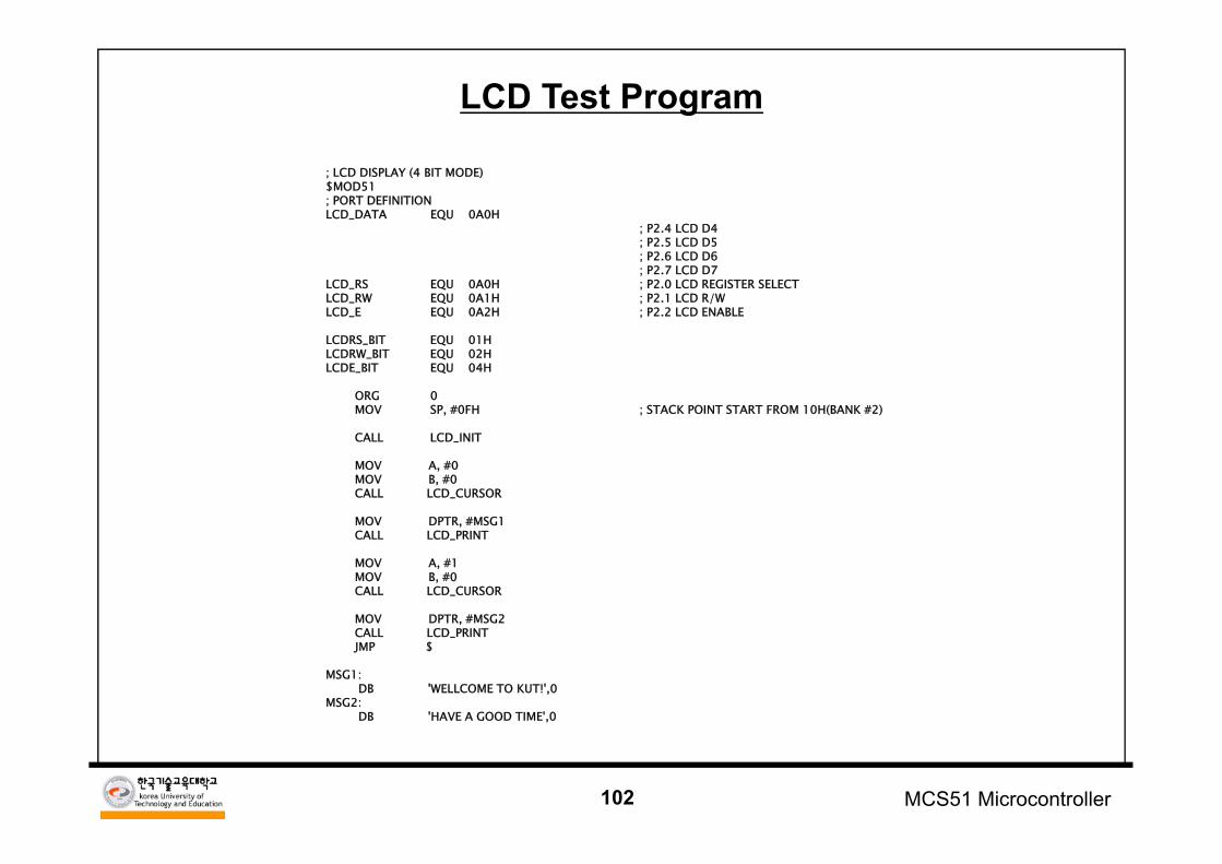
; LCD DISPLAY (4 BIT MODE)$MOD51; PORT DEFINITIONLCD_DATA EQU 0A0H
; P2.4 LCD D4; P2.5 LCD D5; P2.6 LCD D6; P2.7 LCD D7
LCD_RS EQU 0A0H ; P2.0 LCD REGISTER SELECTLCD_RW EQU 0A1H ; P2.1 LCD R/WLCD_E EQU 0A2H ; P2.2 LCD ENABLE
LCDRS_BIT EQU 01HLCDRW_BIT EQU 02HLCDE_BIT EQU 04H
ORG 0MOV SP, #0FH ; STACK POINT START FROM 10H(BANK #2)
CALL LCD_INIT
MOV A, #0MOV B, #0CALL LCD_CURSOR
MOV DPTR, #MSG1CALL LCD_PRINT
MOV A, #1MOV B, #0CALL LCD_CURSOR
MOV DPTR, #MSG2CALL LCD_PRINTJMP $
MSG1:DB 'WELLCOME TO KUT!',0
MSG2:DB 'HAVE A GOOD TIME',0
LCD Test Program
103 MCS51 Microcontroller
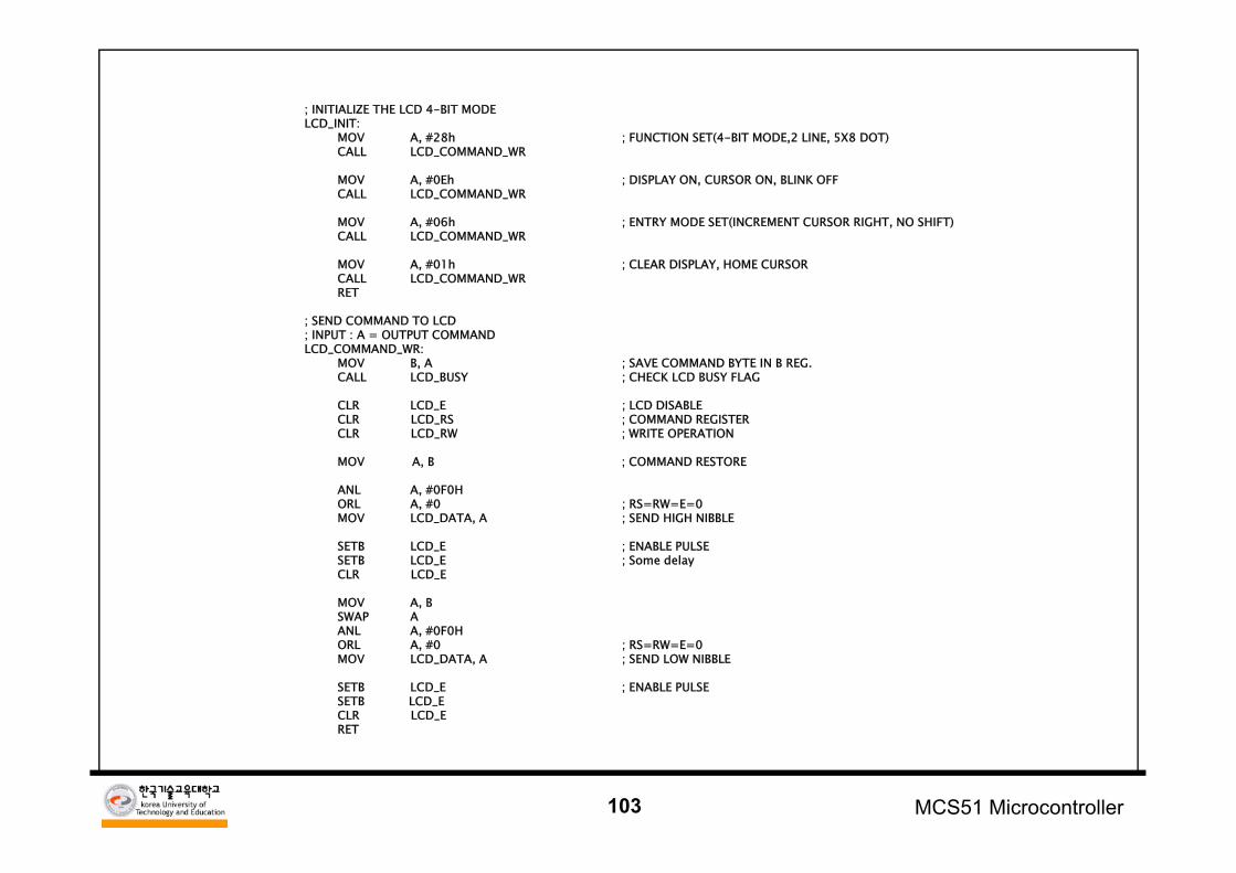
; INITIALIZE THE LCD 4-BIT MODELCD_INIT:
MOV A, #28h ; FUNCTION SET(4-BIT MODE,2 LINE, 5X8 DOT) CALL LCD_COMMAND_WR
MOV A, #0Eh ; DISPLAY ON, CURSOR ON, BLINK OFFCALL LCD_COMMAND_WR
MOV A, #06h ; ENTRY MODE SET(INCREMENT CURSOR RIGHT, NO SHIFT)CALL LCD_COMMAND_WR
MOV A, #01h ; CLEAR DISPLAY, HOME CURSORCALL LCD_COMMAND_WRRET
; SEND COMMAND TO LCD; INPUT : A = OUTPUT COMMANDLCD_COMMAND_WR:
MOV B, A ; SAVE COMMAND BYTE IN B REG.CALL LCD_BUSY ; CHECK LCD BUSY FLAG
CLR LCD_E ; LCD DISABLECLR LCD_RS ; COMMAND REGISTERCLR LCD_RW ; WRITE OPERATION
MOV A, B ; COMMAND RESTORE
ANL A, #0F0HORL A, #0 ; RS=RW=E=0MOV LCD_DATA, A ; SEND HIGH NIBBLE
SETB LCD_E ; ENABLE PULSESETB LCD_E ; Some delayCLR LCD_E
MOV A, BSWAP AANL A, #0F0HORL A, #0 ; RS=RW=E=0MOV LCD_DATA, A ; SEND LOW NIBBLE
SETB LCD_E ; ENABLE PULSE SETB LCD_ECLR LCD_E RET
104 MCS51 Microcontroller
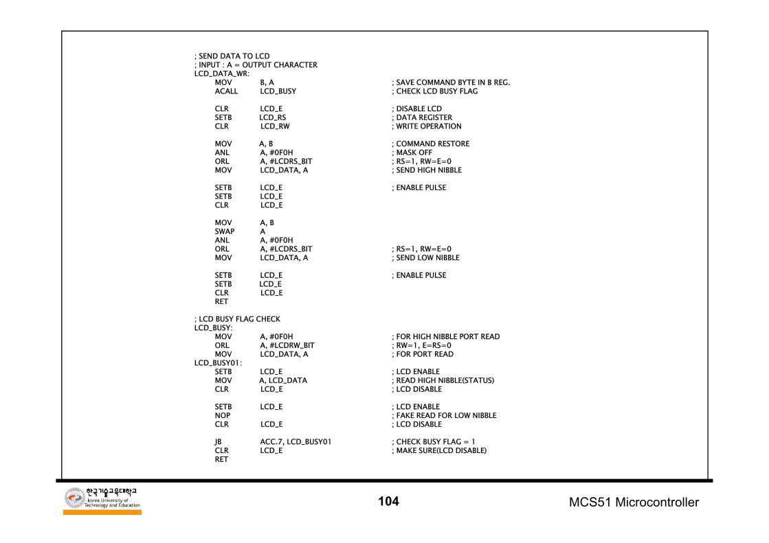
; SEND DATA TO LCD; INPUT : A = OUTPUT CHARACTERLCD_DATA_WR:
MOV B, A ; SAVE COMMAND BYTE IN B REG.ACALL LCD_BUSY ; CHECK LCD BUSY FLAG
CLR LCD_E ; DISABLE LCDSETB LCD_RS ; DATA REGISTERCLR LCD_RW ; WRITE OPERATION
MOV A, B ; COMMAND RESTOREANL A, #0F0H ; MASK OFFORL A, #LCDRS_BIT ; RS=1, RW=E=0MOV LCD_DATA, A ; SEND HIGH NIBBLE
SETB LCD_E ; ENABLE PULSESETB LCD_ECLR LCD_E
MOV A, BSWAP AANL A, #0F0HORL A, #LCDRS_BIT ; RS=1, RW=E=0MOV LCD_DATA, A ; SEND LOW NIBBLE
SETB LCD_E ; ENABLE PULSESETB LCD_E CLR LCD_ERET
; LCD BUSY FLAG CHECK LCD_BUSY:
MOV A, #0F0H ; FOR HIGH NIBBLE PORT READORL A, #LCDRW_BIT ; RW=1, E=RS=0MOV LCD_DATA, A ; FOR PORT READ
LCD_BUSY01:SETB LCD_E ; LCD ENABLEMOV A, LCD_DATA ; READ HIGH NIBBLE(STATUS)CLR LCD_E ; LCD DISABLE
SETB LCD_E ; LCD ENABLENOP ; FAKE READ FOR LOW NIBBLECLR LCD_E ; LCD DISABLE
JB ACC.7, LCD_BUSY01 ; CHECK BUSY FLAG = 1CLR LCD_E ; MAKE SURE(LCD DISABLE)RET
105 MCS51 Microcontroller
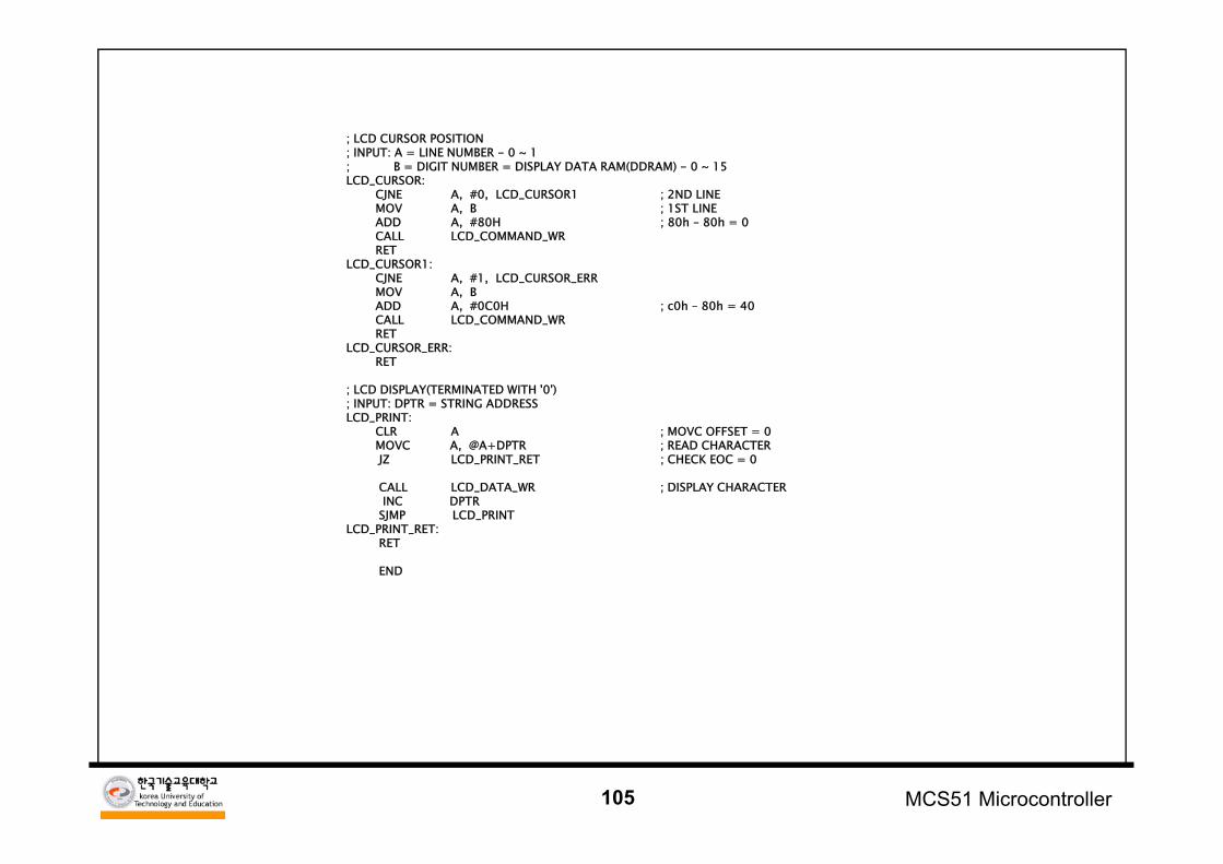
; LCD CURSOR POSITION; INPUT: A = LINE NUMBER - 0 ~ 1; B = DIGIT NUMBER = DISPLAY DATA RAM(DDRAM) - 0 ~ 15LCD_CURSOR:
CJNE A, #0, LCD_CURSOR1 ; 2ND LINEMOV A, B ; 1ST LINEADD A, #80H ; 80h – 80h = 0CALL LCD_COMMAND_WRRET
LCD_CURSOR1:CJNE A, #1, LCD_CURSOR_ERRMOV A, BADD A, #0C0H ; c0h – 80h = 40CALL LCD_COMMAND_WRRET
LCD_CURSOR_ERR:RET
; LCD DISPLAY(TERMINATED WITH '0'); INPUT: DPTR = STRING ADDRESS LCD_PRINT:
CLR A ; MOVC OFFSET = 0MOVC A, @A+DPTR ; READ CHARACTER JZ LCD_PRINT_RET ; CHECK EOC = 0
CALL LCD_DATA_WR ; DISPLAY CHARACTERINC DPTR
SJMP LCD_PRINT LCD_PRINT_RET:
RET
END
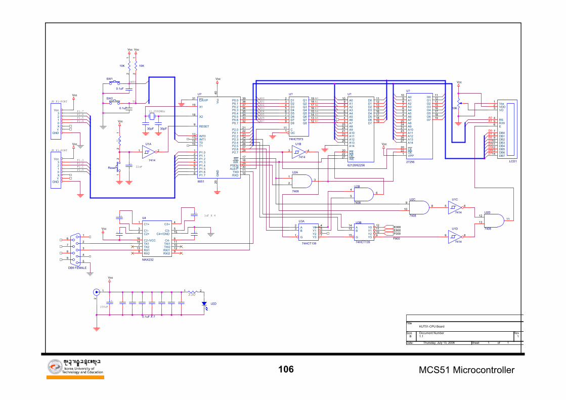
106 MCS51 Microcontroller
EA/VP31
X119
X218
RESET9
INT012
INT113
T014
T115
P1.01
P1.12
P1.23
P1.34
P1.45
P1.56
P1.67
P1.78
P0.0 39
P0.138
P0.237
P0.3 36
P0.4 35
P0.534
P0.6 33
P0.7 32
P2.021
P2.1 22
P2.2 23
P2.324
P2.425
P2.5 26
P2.6 27
P2.728
RD 17
WR 16
PSEN29
ALE/P30
TXD 11
RXD 10
Vcc
40G
ND
20
U?
8051
Title
Size Document Number Rev
Date: Sheet of
1.1 1
KUT51-CPU Board
B
1 1Thursday, July 13, 2006
A010
A19
A28
A37
A46
A55
A64
A73
A825
A924
A1021
A1123
A122
A1326
A1427
CE20
OE22
VPP1
O0 11
O1 12
O213
O315
O4 16
O5 17
O618
O7 19
U?
27256
LED
T0
INT0SW1
SW2
F000
1 2
U1A
7414
AD2AD1AD0
AD7AD6AD5
AD3AD4
+
A6
A4A5
A2A1
A3
A0
5
4
3
2
1
9
8
7
6
DB9 FEMALE
A2
B3
G1
Y04
Y15
Y2 6
Y3 7
U3A
74HCT139
P1.2P1.3
A7
P1.0P1.1
100uF
Vss1
VDD2
VO3
RS4
R/W5
E6
DB07
DB18
DB29
DB310
DB411
DB512
DB613
DB714
LCD1
1
2
12
0.1uF
0.1uF
C1+1
C1-3
C2+2
C2-/VCC16
TX114
TX27
RX113
RX28
RXI29RXI1 12TXI2 10TXI111C4-6
C4+/GND 15C3-5
C3+ 4U4
MAX232
A010
A19
A28
A37
A46
A55
A64
A73
A825
A924
A1021
A1123
A122
A1326
A141
CS20
OE22
WE27
D0 11
D112
D213
D3 15
D4 16
D517
D6 18
D7 19
U?
62128/62256
Vcc3210XY
GND
12
10K
Vcc
10KVcc3210XY
GND
+
12
Reset
11.0592MHz
1uF X 4
JP P1-PORT
Vcc
Vcc
10K
A0
1
23
U2A
7408
22uF
A1
Vcc
Vcc
Vcc
Vcc
E800E000
0.1uF X 7
Vcc
Vcc
12
10K
Vcc
D0
P1.6P1.7
P1.4P1.5
D1
30pF 30pF
D2
JP P1-PORT
D3
++
++
D4
D12
D23
D34
D45
D56
D67
D78
D89
C11
OC1
Q1 19
Q218
Q317
Q4 16
Q5 15
Q614
Q7 13
Q8 12
U?
74HCT573
D5
F800
D63 4
U1B
7414D7
5 6
U1C
7414
9 8
U1D
7414
1 2
4
56
U2B
7408 9
108
U2C
7408
330
12
1311
U2D
7408A14
B13
G15
Y012
Y111
Y2 10
Y3 9
U3B
74HCT139