Embed Size (px)
Citation preview
T H E D I S R U P T I V E S E M I C O N D U C T O R T E C H N O L O G I E S M A G A Z I N E
INSIDE 3
COWIN helps Sensaris certify the ZAO biomedical sensor
EQUIPMENT & MATERIALS 4
Enabling leading-edge devices: DRIE today
NANOTECHNOLOGY 10
Graphene researchers create superheated water that can corrode diamonds
Free registration on www.i-micronews.com
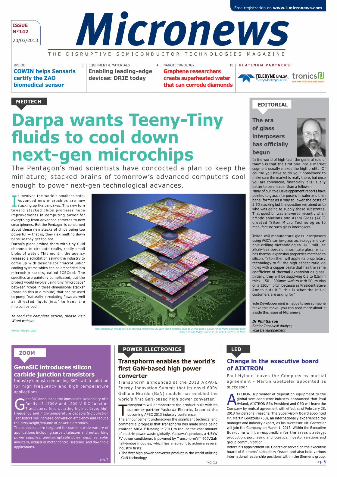
It involves the world’s smallest bath. Advanced new microchips are now stacking up like pancakes. This new turn
toward s tacked chips promises huge improvements in computing power for everything from advanced cameras to new smartphones. But the Pentagon is concerned about these new stacks of chips being too powerful — that is, they risk melting down because they get too hot.Darpa’s plan: embed them with tiny fluid channels to circulate really, really small blobs of water. This month, the agency released a solicitation asking the industry to come up with designs for “microfluidic” cooling systems which can be embedded into microchip stacks, called ICECool. The specifi cs are painfully complicated, but the project would involve using tiny “microgaps” between “chips in three-dimensional stacks” (more on this in a minute) that can be used to pump “naturally-circulating fl ows as well as d i r ec ted l iqu id je t s ” to keep the microchips cool.
To read the complete article, please visit Wired website.
www.wired.com
Darpa wants Teeny-Tiny fl uids to cool down next-gen microchips The Pentagon’s mad scientists have concocted a plan to keep the miniature; stacked brains of tomorrow’s advanced computers cool enough to power next-gen technological advances.
EDITORIALMEDTECH
POWER ELECTRONICS
P L A T I N U M P A R T N E R S :
Everywhereyoulook™
This conceptual image for 3-D stacked microchips by IBM could possibly lead to a chip that’s 1,000 times more powerful than what’s in use today. But is it too hot? Courtesy of IBM)
Transphorm will demonstrate the product built with its customer-partner Yaskawa Electric, Japan at the upcoming APEC 2013 industry conference.
The announcement underscores the signifi cant technical and commercial progress that Transphorm has made since being awarded ARPA-E funding in 2011,to reduce the vast amount of electric power waste globally. Yaskawa’s product, a 4.5kW PV power conditioner, is powered by Transphorm’s™ 600VGaN half-bridge modules, which has enabled it to achieve several industry fi rsts:• The fi rst high power converter product in the world utilizing
GaN technology>p.12
Transphorm enables the world’s fi rst GaN-based high power converterTransphorm announced at the 2013 ARPA-E Energy Innovation Summit that its novel 600V Gallium Nitride (GaN) module has enabled the world’s first GaN-based high power converter.
In the world of high tech the general rule of thumb is that the first one into a market segment usually makes the high profi ts. Of course you have to do your homework to make sure the market is really there, but once you are convinced, financially it is usually better to be a leader than a follower. Many of our Yole Développement reports have pointed to glass interposers in wafer and then panel format as a way to lower the costs of 2.5D stacking but the question remained as to who was going to supply these substrates. That question was answered recently when nMode solutions and Asahi Glass (AGC) created Triton Micro Technologies to manufacture such glass interposers.
Triton will manufacture glass interposers using AGC’s carrier-glass technology and via-hole drilling methodologies. AGC will use alkali-free boroaluminosilicate glass which has thermal expansion properties matched to silicon. Triton then will apply its proprietary technology to fill the high-aspect-ratio via holes with a copper paste that has the same coefficient of thermal expansion as glass. Initially, they will be supplying 0.3 to 0.5mm thick, 150 – 300mm wafers with 50μm vias on a 130μm pitch because as President Steve Annas puts it “..this is what the initial customers are asking for”
Yole Développement is happy to see someone make this move…you can read more about it inside this issue of Micronews.
Dr Phil GarrouSenior Technical Analyst,Yole Développement
The era of glass interposers has offi cially begun
ISSUEN°142
20/03/2013
GeneSiC announces the immediate availability of a family of 1700V and 1200 V SiC Junc t ion Transistors. Incorporating high voltage, high
frequency and high-temperature capable SiC Junction Transistors will increase conversion effi ciency and reduce the size/weight/volume of power electronics. These devices are targeted for use in a wide variety of applications including server, telecom and networking power supplies, uninterruptable power supplies, solar inverters, industrial motor control systems, and downhole applications.
>p.7
GeneSiC introduces silicon carbide junction transistorsIndustry’s most compelling SiC switch solution for high f requency and high temperature applications.
ZOOMLED
Change in the executive board of AIXTRONPaul Hyland leaves the Company by mutual agreement - Mar t in Goetzeler appointed as successor.
AIXTRON, a provider of deposition equipment to the global semiconductor industry announced that Paul Hyland, AIXTRON SE’s President and CEO will leave the
Company by mutual agreement with effect as of February 28, 2013 for personal reasons. The Supervisory Board appointed Mr. Martin Goetzeler (50), an internationally experienced top manager and industry expert, as his successor. Mr. Goetzeler will join the Company on March 1, 2013. Within the Executive Board, he will be responsible for the areas strategy, production, purchasing and logistics, investor relations and group communication.Before his appointment Mr. Goetzeler served on the executive board of Siemens’ subsidiary Osram and also held various international leadership positions within the Siemens group.
>p.8
2 | ISSUE N°142 | 20/03/2013
G O L D P A R T N E R S
About Yole DéveloppementFounded in 1998, Yole Développement has grown to become a group of companies providing marketing, technology and strategy consulting, media in addition to corporate fi nance services.With a strong focus on emerging applications using silicon and/or micro manufacturing, Yole Développement group has expanded to include more than 50 associates worldwide covering MEMS, Compound Semiconductors, LED, Image Sensors, Optoelectronics, Microfluidics & Medical, Photovoltaics, Advanced Packaging, Nanomaterials and Power Electronics. The group supports industrial companies, investors and R&D organizations worldwide to help them understand markets and follow technology trends to develop their business.
Consulting• Market data, market research & marketing analysis• Technology analysis• Reverse engineering & costing services• Strategy consulting• Patent analysisMore information on www.yole.fr
Reports• Collection of technology & market reports• Players & Market databases• Manufacturing cost simulation tools• Component reverse• Patent analysis• Engineering & Costing analysis
Financial services• Mergers & Acquisitions• Due diligence• Fundraising• Coaching of emerging companies• IP portfolio management & optimizationMore information on www.yolefi nance.com
Media• Online disruptive technologies website:
www.i-micronews.com• Editorial webcasts program• Six magazines: Micronews - MEMS Trends – 3D
Packaging – iLED – Power Dev’ - New in 2013: Image Sensors Industry
• Communication & Webcasts services
ContactsFor more information about:• Consulting & Financial Services : Christophe Fitamant
(fi [email protected])• Reports: David Jourdan ([email protected])• Media & Communication : Sandrine Leroy ([email protected])
CONTENT
INSIDE 3EQUIPMENT & MATERIALS 4MEMS 5MEDTECH 6COMPOUND SEMICONDUCTORS 7LED 8IMAGING 9OPTOELECTRONICS 9PHOTOVOLTAICS 10NANOTECHNOLOGY 10ADVANCED PACKAGING 11POWER ELECTRONICS 12
Editorial StaffBoard Members: Jean-Christophe Eloy - Media Activity, Editor in chief: Dr Eric Mounier - Editors: Alexandre Avron, Frédéric Breussin, Lionel Cadix, Paul Danini, Wen-bin Ding, Dr. Éric Mounier, Pars Mukish, Laurent Robin, Milan Rosina, Benjamin Roussel, Dr. Philippe Roussel - Media & Communication Manager: Sandrine Leroy - Media & Communication Coordinators: Clotilde Fabre, Camille Favre - Layout: atelier JBBOX - Production: Kzen
CONSULTING
TO MEET US
• Taiwan International Lighting Show, March 26 to 29 - Taipei, TaiwanTaiwan International Lighting Show is an exclusive platform for world-class LED Lighting that joins the breakthrough solutions and products, market seminars and even hosts the annual meeting of CIE-Taiwan.More information on www.tils.com.tw • Successful Semiconductor Fabless, April 10 to 12 – Paris, FranceH o w w i l l t h e t e c h n o l o g y e v o l u t i o n i m p a c t t h e semiconductor industry and its supply chain? For the second year, Yole Développement and Serma Technologies have joined forces to organize the Success ful Semiconduc tor Fabless conference, a unique European event dedicated to the fabless business model. To register, please visit www.ssf2013.fr
• 9th International Conference on Concentrator Photovoltaic Systems, April 15 to 17 – Miyazaki, JapanThe “International Conference on Concentrator Photovoltaics,” formerly called the “International Conference on Solar Concentrators for the Generation of Electricity”, provides the opportunity to learn about cutting-edge research, industrialization and the market for concentrating photovoltaic technologies. The scope of the conference is devoted to in-depth technical discussions on the science, engineering, performance and economics of CPV systems.More information on www.cpv-9.org • International Congress on Energy Management Systems and Power Electronics, April 17 to 18 – Tarbes, France2 days to learn and exchange about electrical power, energy management systems, applications on industry and transport fi elds: railway, aerospace, automotive and naval.More information on www.abe-industry.com
20/03/2013 | ISSUE N°142 | 3
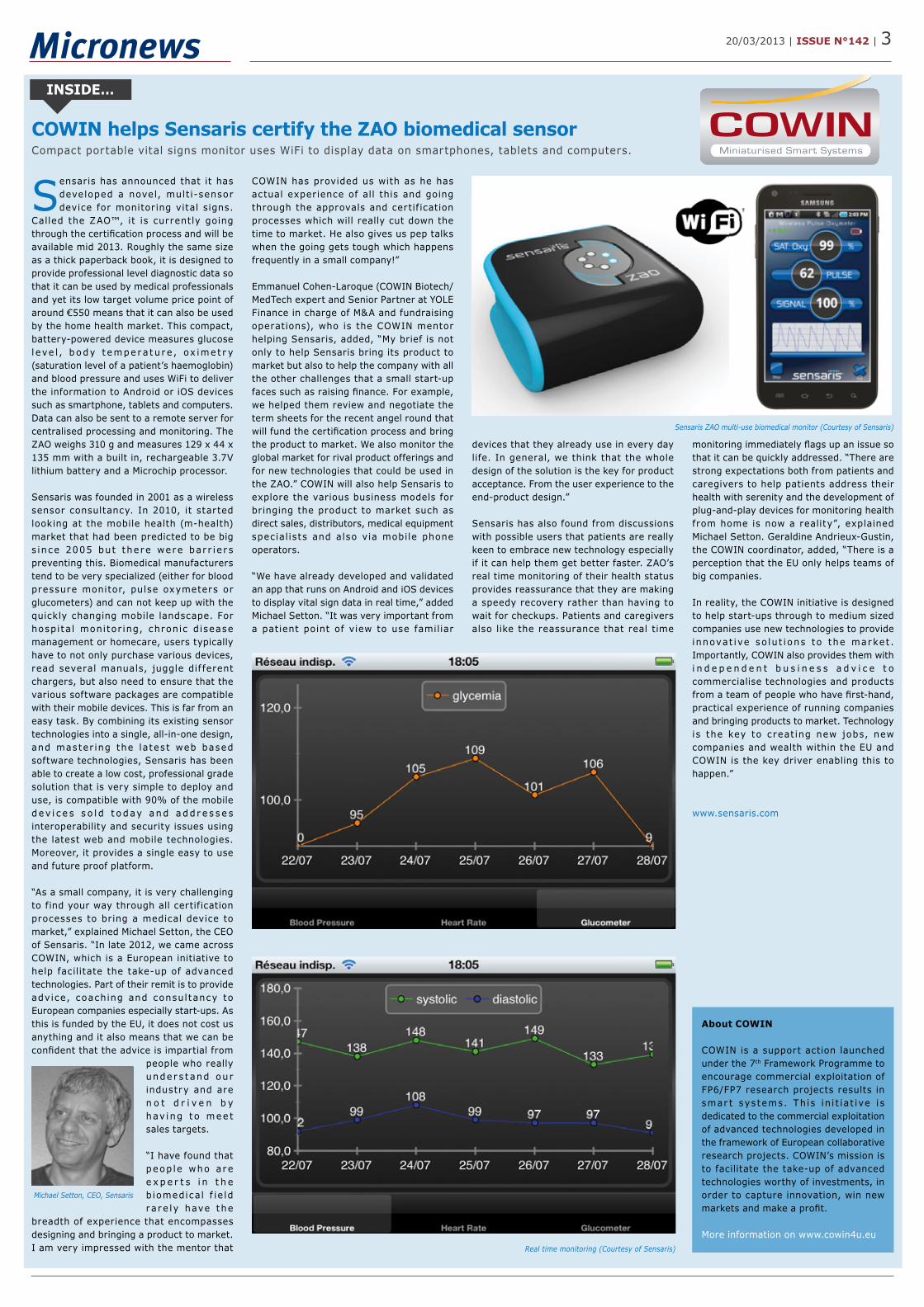
COWIN helps Sensaris certify the ZAO biomedical sensor Compact portable vital signs monitor uses WiFi to display data on smartphones, tablets and computers.
INSIDE…
Sensaris has announced that it has developed a novel, mult i-sensor device for monitoring vital signs.
Called the ZAO™, it is currently going through the certifi cation process and will be available mid 2013. Roughly the same size as a thick paperback book, it is designed to provide professional level diagnostic data so that it can be used by medical professionals and yet its low target volume price point of around €550 means that it can also be used by the home health market. This compact, battery-powered device measures glucose l eve l , b ody t empe r a tu r e , ox ime t r y (saturation level of a patient’s haemoglobin) and blood pressure and uses WiFi to deliver the information to Android or iOS devices such as smartphone, tablets and computers. Data can also be sent to a remote server for centralised processing and monitoring. The ZAO weighs 310 g and measures 129 x 44 x 135 mm with a built in, rechargeable 3.7V lithium battery and a Microchip processor.
Sensaris was founded in 2001 as a wireless sensor consultancy. In 2010, it started looking at the mobile health (m-health) market that had been predicted to be big s ince 2005 but the re were bar r ie r s preventing this. Biomedical manufacturers tend to be very specialized (either for blood pressure monitor, pulse oxymeters or glucometers) and can not keep up with the quickly changing mobile landscape. For hospital monitor ing, chronic disease management or homecare, users typically have to not only purchase various devices, read several manuals, juggle dif ferent chargers, but also need to ensure that the various software packages are compatible with their mobile devices. This is far from an easy task. By combining its existing sensor technologies into a single, all-in-one design, and master ing the lates t web based software technologies, Sensaris has been able to create a low cost, professional grade solution that is very simple to deploy and use, is compatible with 90% of the mobile d ev i c e s s o l d t o day and add r e s s e s interoperability and security issues using the latest web and mobile technologies. Moreover, it provides a single easy to use and future proof platform.
“As a small company, it is very challenging to find your way through all certification processes to bring a medical device to market,” explained Michael Setton, the CEO of Sensaris. “In late 2012, we came across COWIN, which is a European initiative to help facilitate the take-up of advanced technologies. Part of their remit is to provide advice, coaching and consul tancy to European companies especially start-ups. As this is funded by the EU, it does not cost us anything and it also means that we can be confi dent that the advice is impartial from
people who really unde r s t and our industry and are n o t d r i v e n b y hav ing t o mee t sales targets.
“I have found that peop le who ar e e x p e r t s i n t h e b iomedical f ie ld rare ly have the
breadth of experience that encompasses designing and bringing a product to market. I am very impressed with the mentor that
COWIN has provided us with as he has actual experience of all this and going through the approvals and certif ication processes which will really cut down the time to market. He also gives us pep talks when the going gets tough which happens frequently in a small company!”
Emmanuel Cohen-Laroque (COWIN Biotech/MedTech expert and Senior Partner at YOLE Finance in charge of M&A and fundraising operations), who is the COWIN mentor helping Sensaris, added, “My brief is not only to help Sensaris bring its product to market but also to help the company with all the other challenges that a small start-up faces such as raising fi nance. For example, we helped them review and negotiate the term sheets for the recent angel round that will fund the certifi cation process and bring the product to market. We also monitor the global market for rival product offerings and for new technologies that could be used in the ZAO.” COWIN will also help Sensaris to explore the various business models for bringing the product to market such as direct sales, distributors, medical equipment specialists and also via mobile phone operators.
“We have already developed and validated an app that runs on Android and iOS devices to display vital sign data in real time,” added Michael Setton. “It was very important from a patient point of view to use familiar
devices that they already use in every day life. In general, we think that the whole design of the solution is the key for product acceptance. From the user experience to the end-product design.”
Sensaris has also found from discussions with possible users that patients are really keen to embrace new technology especially if it can help them get better faster. ZAO’s real time monitoring of their health status provides reassurance that they are making a speedy recovery rather than having to wait for checkups. Patients and caregivers also like the reassurance that real time
monitoring immediately fl ags up an issue so that it can be quickly addressed. “There are strong expectations both from patients and caregivers to help patients address their health with serenity and the development of plug-and-play devices for monitoring health from home is now a reality”, explained Michael Setton. Geraldine Andrieux-Gustin, the COWIN coordinator, added, “There is a perception that the EU only helps teams of big companies.
In reality, the COWIN initiative is designed to help start-ups through to medium sized companies use new technologies to provide innovat ive so lu t ions to the market . Importantly, COWIN also provides them with i n d e p e n d e n t b u s i n e s s a d v i c e t o commercialise technologies and products from a team of people who have fi rst-hand, practical experience of running companies and bringing products to market. Technology is the key to creat ing new jobs, new companies and wealth within the EU and COWIN is the key driver enabling this to happen.”
www.sensaris.com
About COWIN
COWIN is a support action launched under the 7th Framework Programme to encourage commercial exploitation of FP6/FP7 research projects results in smar t sys tems. Th is in i t ia t ive i s dedicated to the commercial exploitation of advanced technologies developed in the framework of European collaborative research projects. COWIN’s mission is to facilitate the take-up of advanced technologies worthy of investments, in order to capture innovation, win new markets and make a profi t.
More information on www.cowin4u.euReal time monitoring (Courtesy of Sensaris)
Sensaris ZAO multi-use biomedical monitor (Courtesy of Sensaris)
Michael Setton, CEO, Sensaris

4 | ISSUE N°142 | 20/03/2013
EQUIPMENT & MATERIALS
Enabling leading-edge devices: DRIE todayMicronews interviewed Dave Thomas, Ph.D., the Marketing Director of Etch Products at SPTS to get his perspective on today’s market for Bosch-process DRIE equipment. This is his commentary.
Market segment history and statusThe f irst patent for the Bosch switched process for deep reactive ion etch was granted in 1996, and the fi rst licensee for this process was a company that’s now a par t of SPTS. We have del ivered and installed over 1,000 Bosch-process DRIE modules, which makes us the market leader in this technology.
Technology capability enables business driversThe DRIE market makes a strong case for how bet ter tools and process control enables new and better devices. Most people associate DRIE with creating deep trenches, and this capability is important for MEMS devices like inertial sensors. The “state-of-the-art” for our products today includes an etch rate of >30 microns per minute, feature sizes below 50 nanometer line widths, and aspect ratios to 90:1 on 0.4 micron trenches – although not all of these attributes at the same time.
This capability has enabled broad ranges of devices with capabilities only imagined years ago. Highly-sensitive MEMS devices are in high-volume production using our tools and nano-scale devices (NEMS) are in development. Markets for certain products (for example, silicon microphones) are booming and have reached shipping volumes much higher than were predicted several years ago. Autofocus products, such as the ones delivered by DigitalOptics Corp. for the smartphone and tablet camera markets, have requirements for trench etching that could not have been done until recently.
There are other significant market trends driven by DRIE capability. The 2.5D/3D packaging area is making heavy use of through-silicon via (TSV) technology, and DRIE using the highly-sensitive endpoint detection technology in our products plays a key role. Manufacturers are grinding wafers down from the back side, and then etching to expose the TSVs. This “TSV reveal” process is extremely dif f icult, because endpoint detection is critical. Too little etch, and the wafers need to be re-worked. Too much, and the devices are trash.
Backside wafer grinding is a notoriously variable process, but our “ReVia” technology solves this issue by detecting the point at which the TSVs protrude through the silicon. This has been highly successful for customers, especially in the manufacture of high-value stacked TSV wafers.
TSVs are difficult to etch because of the narrower entry aper ture compared to trenches and because aspect ratios can still be in the range 10:1 to 25:1. The usual industry approach is single source power in combination with bias power to the wafer, but the SPTS Rapier product has dual source power plus bias power, with 2 entry points for gas. This gives 2 independently-controlled plasma zones for better uniformity and tilt control.
The signifi cant manufacturing concern is, as always, to dr ive costs down, to make devices in a more controlled manner, and to achieve higher throughput. Our DRIE tools
enable HVM with signifi cant control, thus enabling the highly-precise tilt management I mentioned. This t ight control of t i lt enables the manufacture of these new high-sensitivity inertial sensors with uniform trenches 1-2 microns wide, 10-20:1 aspect ratios, and walls within ±0.1 degree of vertical. Scallop control corresponds to etch rate, and where etch rate can be adequately compromised these can be controlled to less than 5 nm into the Si sidewall.
The future The market for these tools is growing, and the sophistication of the customer needs is growing faster. Customers were in volume
production with Bosch-process DRIE in the 2005 to 2007 timeframe, but their concerns today are very much about “high-use, 90%+ uptime, >1000 hours between wet cleans.” We have engineered an upgrade path for existing customers that can bring them higher throughput, lower CoO and better prof ile control on their existing equipment.
There are “big-picture” market issues in play. At the MEMS Executive Congress held recently in Amsterdam, there was much discussion about MEMS consumer device production exceeding automotive sensor production. Automobiles today are looking
more like consumer devices – some car advertisements are more focused on in-car entertainment than performance – and MEMS device use per vehicle is growing. The end-game is “driver-less” cars, which will be highly dependent on sensors and MEMS devices.
Two MEMS device growth areas to watch are health care, where people are talking about the reality of a “doctor-in-your-watch” product, and new uses of the existing sensor devices in smartphones and tablets; application software growth here will likely be huge. Another possible future use of DRIE will be in other materials like glass, which could enable advanced microfl uidics or lens/optical devices.
At SPTS, we’re optimistic for the future. We see lots of possibilities for DRIE applications, including the possible use of this technology to replace saws and lasers for dicing chips. We see the growing need for temperature and stress control in CVD on MEMS devices, in low-temperature fi lms, and in TSV reveal. Stress control will likely be a great concern in 2.5D and 3D packaging, as well.
The manufacturing issues will continue to be cost of ownership, and quality / precision control. We’re ready.
www.spts.com
SPTS Omega fxP with Pegasus Rapier and DSi modules (Courtesy of SPTS)
Dr. Dave Thomas i s M a r k e t i n g Direc tor for SPTS Technologies’ etch p r o d u c t s . H e i s r e s p o n s i b l e f o r SPTS’s etch product l ine, inc luding al l aspects of marketing, product positioning
and the provision of support to the worldwide sales team.
He joined SPTS (the former Electrotech Equipment Ltd.) in 1994 as a process engineer in physical vapour deposition (PVD) before becoming PVD technology manager, Japan in 1996. He took up his f irst marketing position as product marketing manager for etch products in 1997 and subsequently promoted to Marketing Director for etch products in 2008.
Dr. Thomas actively participates, and presents widely on etch and deposition technologies at global conferences. He has also authored over 30 technical articles and papers.
20/03/2013 | ISSUE N°142 | 5
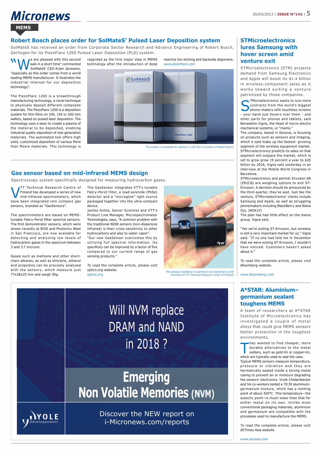
“We are pleased with this second sale in a short time” commented SolMateS’ CEO Arjen Janssens,
“especially as this order comes from a world leading MEMS manufacturer. It illustrates the industr ial interest for our deposit ion technology”.
The PiezoFlare 1200 is a breakthrough manufacturing technology, a novel technique to physically deposit different composite materials. The PiezoFlare 1200 is a deposition system for thin fi lms on 100, 150 or 200 mm wafers, based on pulsed laser deposition. The technology uses a laser to create a plasma of the material to be deposited, enabling industrial quality deposition of new generation materials. The automated tool offers high yield, customized deposition of various More than Moore materials. This technology is
regarded as the first major step in MEMS technology after the introduction of deep
reactive Ion etching and backside alignment.www.piezofl are.com
They wanted to f ind cheaper, more durable alternatives to the metal solders, such as gold-tin or copper-tin,
which are typically used to seal the case.Typical MEMS sensors measure temperature, p r e s sure o r v ib ra t i on and they ar e hermetically sealed inside a strong metal casing to prevent air or moisture degrading the sensors’ electronics. Vivek Chidambaram and his co-workers tested a 70:30 aluminium-germanium mixture, which has a melting point of about 420°C. This temperature—the eutectic point—is much lower than that for e ither metal on its own. Unl ike most conventional packaging materials, aluminium and germanium are compatible with the processes used to manufacture the MEMS.
To read the complete article, please visit EETimes Asia website.
www.eetasia.com
Robert Bosch places order for SolMateS’ Pulsed Laser Deposition systemSolMateS has received an order from Corporate Sector Research and Advance Engineering of Robert Bosch, Gerlingen for its PiezoFlare 1200 Pulsed Laser Deposition (PLD) system.
A*STAR: Aluminium–germanium sealant toughens MEMS A team of researchers at A*STAR Institute of Microelectronics has inves t igated a coup le o f meta l alloys that could give MEMS sensors better protection in the toughest environments.
MEMS
Will NVM replace DRAM and NAND
in 2018 ?
Emerging Non Volatile Memories (NVM)
Discover the NEW report oni-Micronews.com/reports
The system is scheduled for delivery in mid 2013 (Courtesy of Robert Bosch)
STMicroelectronics wants to lure more contracts from the world’s biggest phone-makers with touchless screens
- your hand just hovers over them - and other parts for phones and tablets, said Benedetto Vigna, the Head of micro-electro mechanical systems, or “mems.” The company, based in Geneva, is focusing on products such as sensors and imaging, which it said make up the fastest- growing segment of the wireless equipment market. STMicroelectronics predicts its sales on that segment will outpace the market, which is set to grow grow 19 percent a year to $20 billion by 2016, Vigna said yesterday in an interview at the Mobile World Congress in Barcelona. STMicroelectronics and partner Ericsson AB (ERICB) are weighing options to exit ST-Ericsson. A decision should be announced by the third quarter, they’ve said. Just like the venture, STMicroelectronics’ clients include Samsung and Apple, as well as struggling phonemakers including BlackBerry and Nokia Oyj. (NOK1V) The plan has had little effect on the mems group, Vigna said.
“Yes we’re exiting ST-Ericsson, but wireless is still a very important market for us,” Vigna said. “If no one had told me in December that we were exiting ST-Ericsson, I wouldn’t have noticed. Customers haven’t asked about it.”
To read the complete article, please visit Bloomberg website.
www.bloomberg.com
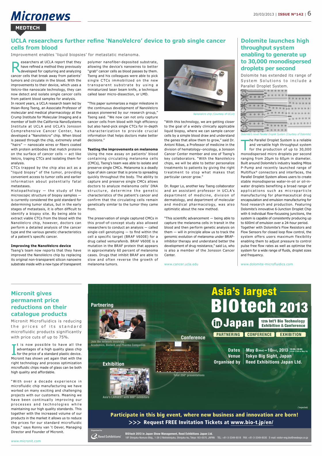
VTT Technical Research Centre of Finland has developed a series of new mid-infrared spectrometers, which
have been integrated into compact gas sensors, branded as “GasSensors”.
The spectrometers are based on MEMS-tunable Fabry-Perot fi lter spectral sensors. The fi rst demonstrator sensors, which were shown recently at BiOS and Photonics West in San Francisco, are now available for detect ing and analyzing low levels of hydrocarbon gases in the spectrum between 3 and 3.7 microns.
Gases such as methane and other short-chain alkanes, as well as ethylene, ethanol and propylene can be precisely analyzed with the sensors, which measure just 77x38x25 mm and weigh 95g.
The GasSensor integrates VTT’s tunable Fabry-Perot filter, a lead-selenide (PbSe) detector and a “microglow” light source packaged together into the ultra-compact device.Jarkko Antila, Senior Scientist and VTT’s Product Line Manager, Microspectrometer Technologies, says, “A common problem with the traditional NDIR sensors (non-dispersive infrared) is their cross sensitivity to other hydrocarbons and also to water vapor”.“Our new GasSensor overcomes this by uti l izing ful l spectral information. Its specifi city can be improved by a factor of fi ve compared to our current range of gas sensing products.”
To read the complete article, please visit optics.org website.optics.org
STMicroelectronics lures Samsung with hover screen amid venture exitSTMicroelectronics (STM) projects demand from Samsung Electronics and Apple will boost its $1.4 billion in wireless-component sales as it works toward ex i t ing a venture patronized by those companies.
Gas sensor based on mid-infrared MEMS designSpectroscopy system specifically designed for measuring hydrocarbon gases.
The compact GasSensor is claimed to be insensitive to drift (Courtesy of VTT Technical Research Center of Finland)
20/03/2013 | ISSUE N°142 | 6
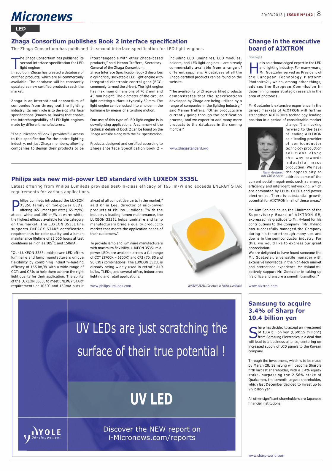
Researchers at UCLA report that they have refi ned a method they previously developed for capturing and analyzing
cancer cells that break away from patients’ tumors and circulate in the blood. With the improvements to their device, which uses a Velcro-like nanoscale technology, they can now detect and isolate single cancer cells from patient blood samples for analysis.In recent years, a UCLA research team led by Hsian-Rong Tseng, an Associate Professor of molecular and medical pharmacology at the Crump Institute for Molecular Imaging and a member of both the California NanoSystems Institute at UCLA and UCLA’s Jonsson Comprehens ive Cance r Cente r, has developed a “NanoVelcro” chip. When blood is passed through the chip, extremely small “hairs” — nanoscale wires or fi bers coated with protein antibodies that match proteins on the surface of cancer cells — act like Velcro, traping CTCs and isolating them for analysis.CTCs trapped by the chip also act as a “liquid biopsy” of the tumor, providing convenient access to tumor cells and earlier i n f o rmat i on abou t po ten t ia l l y f a t a l metastases.H i s t opa tho logy — the s tudy o f t he microscopic structure of biopsy samples — is currently considered the gold standard for determining tumor status, but in the early stages of metastasis, it is often diffi cult to identify a biopsy site. By being able to extract viable CTCs from the blood with the NanoVelcro chip, however, doctors can perform a detailed analysis of the cancer type and the various genetic characteristics of a patient’s specifi c cancer.
Improving the NanoVelcro deviceTseng’s team now reports that they have improved the NanoVelcro chip by replacing its original non-transparent silicon nanowire substrate inside with a new type of transparent
polymer nanofiber-deposited substrate, allowing the device’s nanowires to better “grab” cancer cells as blood passes by them.Tseng and his colleagues were able to pick s ingle CTCs immobi l ized on the new t r a n s p a r e n t s u b s t r a t e b y u s i n g a miniaturized laser beam knife, a technique called laser micro-dissection, or LMD.
“This paper summarizes a major milestone in the continuous development of NanoVelcro assays pioneered by our research group,” Tseng said. “We now can not only capture cancer cells from blood with high effi ciency but also hand-pick single CTCs for in-depth c harac te r i z a t i on to p r ov ide c r uc ia l information that helps doctors make better decisions.”
Testing the improvements on melanomaUsing the new assay on patients’ blood containing circulating melanoma cells (CMCs), Tseng’s team was able to isolate and preserve single CMCs. Melanoma is a deadly type of skin cancer that is prone to spreading quickly throughout the body. The ability to capture and preserve single CMCs allows doctors to analyze melanoma cells’ DNA s t r u c t u r e , d e t e r m i n e t h e g e n e t i c characteristics of the patient’s cancer and confirm that the circulating cells remain genetically similar to the tumor they came from.
The preservation of single captured CMCs in this proof-of-concept study also allowed researchers to conduct an analysis — called single-cell genotyping — to fi nd within the cell a specific target (BRAF V600E) for a drug called vemurafenib. BRAF V600E is a mutation in the BRAF protein that appears in approximately 60 percent of melanoma cases. Drugs that inhibit BRAF are able to slow and of ten reverse the growth of melanoma tumors.
“With this technology, we are getting closer to the goal of a widely clinically applicable liquid biopsy, where we can sample cancer cells by a simple blood draw and understand the genes that allow them to grow,” said Dr. Antoni Ribas, a Professor of medicine in the division of hematology–oncology, a Jonsson Cancer Center member and one of Tseng’s key collaborators. “With the NanoVelcro chips, we will be able to better personalize treatments to patients by giving the right t r eatment to s top what makes that particular cancer grow.”
Dr. Roger Lo, another key Tseng collaborator and an assistant professor in UCLA’s depar tment o f medic ine, d iv is ion o f dermatology, and department of molecular and medical pharmacology, was also optimistic about the new method.
“This scientifi c advancement — being able to capture the melanoma cells in transit in the blood and then perform genetic analysis on them — will in principle allow us to track the genomic evolution of melanoma under BRAF-inhibitor therapy and understand better the development of drug resistance,” said Lo, who is also a member of the Jonsson Cancer Center.
www.cancer.ucla.edu
It is now poss ib le to have a l l the advantages of a high quality glass chip for the price of a standard plastic device.
Micronit has shown yet again that with the right technology and process optimization microfl uidic chips made of glass can be both high quality and affordable.
“W i th ove r a de c ade expe r i ence in microfluidic chip manufacturing we have worked on many exciting and challenging projects with our customers. Meaning we have been cont inual ly improving our p r o c e s s e s a n d t e c h n o l o g i e s wh i l e maintaining our high quality standards. This together with the increased volume of our products in the market it allows us to reduce the prices for our standard microfluidic chips.” says Ronny van ‘t Oever, Managing Director and Founder of Micronit.
www.micronit.com
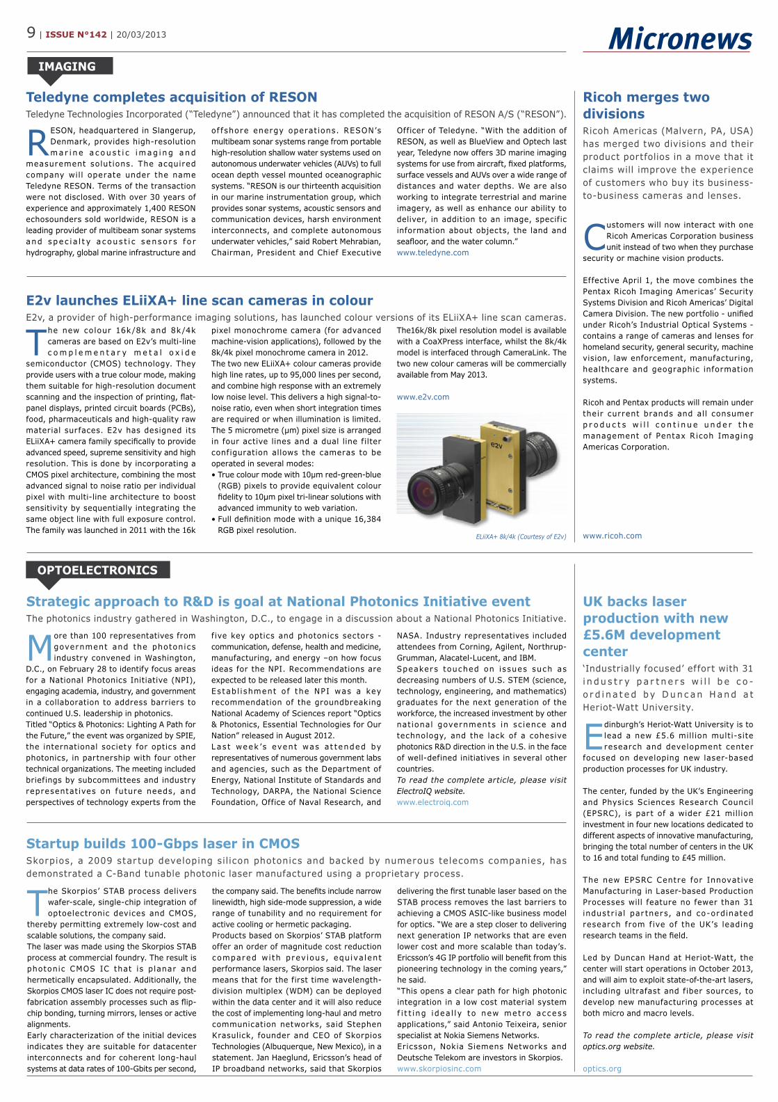
The Parallel Droplet System is a reliable and versatile high throughput system for the production of up to 30,000
monodispersed micro droplets per second ranging from 20μm to 60μm in diameter. Built around Dolomite’s industry leading Mitos P-Pump and recently launched range of Multiflux® connectors and interfaces, the Parallel Droplet System allows users to create stable monodisperse water-in-oil or oil-in-water droplets benefiting a broad range of app l i c a t i ons suc h a s m i c r opa r t i c l e manufacturing for pharmaceutical drug encapsulation and emulsion manufacturing for food research and production. Featuring Dolomite’s innovative 6-Junction Droplet Chip with 6 individual fl ow-focussing junctions, the system is capable of consistently producing up to 600ml of emulsion over a 24-hour period.Together with Dolomite’s Flow Resistors and Flow Sensors for closed loop fl ow control, the system offers users maximum flexibility enabling them to adjust pressure to control pulse free fl ow rates as well as optimise the system for a wide range of fl uids, droplet sizes and frequency.
www.dolomite-microfl uidics.com
UCLA researchers further refi ne ‘NanoVelcro’ device to grab single cancer cells from blood Improvement enables ‘liquid biopsies’ for metastatic melanoma.
Micronit gives permanent price reductions on their catalogue products Micronit Microf luidics is reducing t h e p r i c e s o f i t s s t a n d a r d microf luidic products signif icantly with price cuts of up to 75%.
Dolomite launches high throughput system enabling to generate up to 30,000 monodispersed droplets per secondDolomite has extended its range of Sys tem So lu t i ons t o i n c lude a Parallel Droplet System.
MEDTECH
NanoVelcro chip (Courtesy of UCLA)
Dolomite’s novel Parallel Droplet System (Courtesy of Dolomite)

7 | ISSUE N°142 | 20/03/2013
COMPOUND SEMICONDUCTORS
GeneSiC Semiconductor, a pioneer and global supplier of a broad range of S i l i c o n C a r b i d e (S i C ) p o w e r
semiconductors announces the immediate availability of its second generation hybrid mini-modules using 1200 V/100 Amperes SiC Schottky Rectifi ers with rugged Silicon IGBTs – the GB100XCP12-227. The performance-price point at which this product is being released allows many power conversion applications to benefi t from the reduction of the cost/size/weight/volume that neither Silicon IGBT/ Silicon Rectifi er solution, nor a pure SiC Module can offer. These devices are targeted for use in a wide var iety of applications including industrial motors, solar inverters, specialized equipment and power grid applications.
GT Advanced Technologies and Soitec announced a development agreement and a licensing agreement allowing GT to develop, manufacture and commercialize a high-volume, multi-wafer HVPE system to produce high-quality GaN epi layers on substrates used in the LED and other growth industries such as power electronics. The higher growth rates and improved material properties made possible by the HVPE system are expected to signifi cantly reduce process costs while boosting device performance compared with the traditional
MOCVD process. Initial pre-payment of the licensing fees as outlined in the agreement is already underway, but further specifi c terms were not disclosed.
G T w i l l d eve l op, manu f a c t u r e and commercialize the HVPE system incorporating Soitec Phoenix Labs’ (a subsidiary of Soitec) unique and proprietary HVPE technology including its novel and advanced source delivery system that is expected to lower the costs of precursors delivered to the HVPE reactor. The HVPE system will enable the production of GaN template sapphire substrates at scale. The expected target date for the commercial availability of the HVPE system is the second half of 2014. “We have been working for more than 6 years on GaN epi processes and have created this breakthrough HVPE technology critical in producing high-quality and low cost GaN layers on sapphire substrates,” said Chantal Arena, VP and general manager of Soitec Phoenix Labs.
“The development and license agreements we are announcing with GT is the ultimate validation of this work and builds on the agreement we announced last year with Silian to integrate a HVPE-based technology on their sapphire. This allows Soitec to structure its LED lighting offer around differentiated technologies and industrial partners that includes materials and equipment. Soitec Phoenix Labs deep know-how in epitaxy technologies and GaN materials will be a key factor to enable GT to bring a revolutionary HVPE system to the market.”
“GT has a successful track record of delivering innovative equipment that has changed industries such as solar PV and LED,” said Tom Gutierrez, GT’s president and CEO.
www.genesicsemi.com
Hybrid SiC Schottky rectifi er/Si IGBT modules from GeneSiC enables 175°C operationLow inductance, higher temperature capability of co-packaged mini-modules pushes IGBTs into new applications.
2013 PROGRAM:
April 9IGBT business trends:
toward an IGBTcentric power
electronic industry?
May 14Non mainstream
packaging in MEMS, LED, Power Electronics…
SiC: more devices,more business and more applications
To watch the webcast, please go to www.i-micronews.com and access the Archives Webcast section
Powered by: Hosted by:
Editorial Webcast available today
Watch it now
Could excess capacity
trigger massive
consolidation?
Discover the NEWreport on
i-Micronews.com/reports
Sapphire Substrates
2013
1200 V/100 A Si IGBT/SiC rectifi er (Courtesy of GeneSiC)
Junction transistors offered by GeneSiC exhibit ultra-fast switching capability, a square reverse biased safe operation area
(RBSOA), as well as temperature-independent transient energy losses and switching times. These switches are gate-oxide free, normally-off, exhibit positive temperature co-effi cient of on-resistance, and are capable of being driven by commercial, commonly available 15 V IGBT gate drivers, unlike other SiC switches.
While offering compatibility with SiC JFET drivers, junction transistors can be easily paralleled because of their matching transient characteristics.
“As power system designers continue to push the limits of operating frequency, while still demanding high circuit effi ciencies, they need SiC switches which can offer a standard of performance and production uniformity. Utilizing the unique device and fabrication innovations, GeneSiC’s transistor products help designers achieve all that in a more robust solution,” said Dr. Ranbir Singh, President of GeneSiC Semiconductor.
1700 V junction transistor technical highlights• T h r e e o f f e r i n g s – 110 m O h m s
(G A 1 6 J T 1 7 - 2 4 7 ) ; 2 5 0 m O h m s (GA08JT17-247); and 500 mOhms (GA04JT17-247)
• Tjmax = 175oC • Turn On/Of f; R ise/Fal l T imes <50 nanoseconds typical.
1200 V junction transistor technical highlights• Tw o o f f e r i n g s – 2 2 0 m O h m s
(GA06JT12-247); and 460 mOhms (GA03JT12-247)
• Tjmax = 175oC • Turn On/Of f; R ise/Fal l T imes <50
nanoseconds typical
All devices are 100% tested to full voltage/current ratings and housed in Halogen-Free, RoHS compliant TO-247 packages. The devices are immediately available from GeneSiC’s authorized distributors.
www.genesicsemi.com
GeneSiC introduces silicon carbide junction transistorsFrom page 1
ZOOM
Silicon Carbide Junction Transistors (Courtesy of GeneSiC)
20/03/2013 | ISSUE N°142 | 8
LED
Zhaga Consortium publishes Book 2 interface specifi cationThe Zhaga Consortium has published its second interface specification for LED light engines.
Philips sets new mid-power LED standard with LUXEON 3535L Latest offering from Philips Lumileds provides best-in-class eff icacy of 165 lm/W and exceeds ENERGY STAR requirements for various applications.
Change in the executive board of AIXTRONFrom page 1
The Zhaga Consortium has published its second interface specifi cation for LED light engines.
In addition, Zhaga has created a database of certifi ed products, which are all commercially available. The database will be constantly updated as new certifi ed products reach the market.
Zhaga is an international consortium of companies from throughout the lighting industry. Its main role is to develop interface specifi cations (known as Books) that enable the interchangeability of LED light engines made by different manufacturers.
“The publication of Book 2 provides full access to this specification for the entire lighting industry, not just Zhaga members, allowing companies to design their products to be
interchangeable with other Zhaga-based products,” said Menno Treffers, Secretary-General of the Zhaga Consortium.Zhaga Interface Specifi cation Book 2 describes a cylindrical, socketable LED light engine with integrated electronic control gear (ECG, commonly termed the driver). The light engine has maximum dimensions of 70.2 mm and 45 mm height. The diameter of the circular light-emitting surface is typically 59 mm. The light engine can be locked into a holder in the luminaire by means of a twisting motion.
One use of this type of LED light engine is in downlighting applications. A summary of the technical details of Book 2 can be found on the Zhaga website along with the full specifi cation.
Products designed and certifi ed according to Zhaga Interface Specif ication Book 2 –
including LED luminaires, LED modules, holders, and LED light engines – are already commercially available from a range of different suppliers. A database of all the Zhaga-certifi ed products can be found on the website.
“The availability of Zhaga-certifi ed products demonstrates that the spec if icat ions developed by Zhaga are being utilized by a range of companies in the lighting industry,” said Menno Treffers. “Other products are currently going through the certification process, and we expect to add many more products to the database in the coming months.”
www.zhagastandard.org
Philips Lumileds introduced the LUXEON 3535L family of mid-power LEDs, offering 165 lumens per watt (165 lm/W)
at cool white and 150 lm/W at warm white, the highest effi cacy available for the category on the market. The LUXEON 3535L line suppor ts ENERGY STAR® cer t i f icat ion requirements for color quality and a lumen maintenance lifetime of 35,000 hours at test conditions as high as 105˚C and 150mA.
“Our LUXEON 3535L mid-power LED offers luminaire and lamp manufacturers unique flexibility by combining industry-leading efficacy of 165 lm/W with a wide range of CCTs and CRIs to help them achieve the right light quality for their application. The ability of the LUXEON 3535L to meet ENERGY STAR®
requirements at 105˚C and 150mA puts it
ahead of all competitive parts in the market,” said Khim Lee, director of mid-power products at Philips Lumileds. “With the industry’s leading lumen maintenance, the LUXEON 3535L helps luminaire and lamp manufacturers bring a quality product to market that meets the application needs of their customers.”
To provide lamp and luminaire manufacturers with maximum fl exibility, LUXEON 3535L mid-power LEDs are available across a full range of CCT (2700K – 6500K) and CRI (70, 80 and 90 CRI) combinations. The LUXEON 3535L is already being widely used in retrofit A19 bulbs, TLEDs, and several offi ce, indoor area lighting and retail applications.
www.philipslumileds.com
He is an acknowledged expert in the LED and lighting industry. For many years, Mr. Goetzeler served as President of
t h e Eu r opean Te c hno l ogy P l a t f o r m Photonics21, which, among other things, advises the European Commiss ion in determining major strategic research in the area of photonics.
Mr Goetzeler’s extensive experience in the target markets of AIXTRON will further strengthen AIXTRON‘s technology leading position in a period of considerable market
change: “I am looking forward to the task of leading AIXTRON as a leading provider o f s em i c onduc to r technology production s o l u t i o n s a l o n g t h e way t owar d s i n d u s t r i a l m a s s production. We have the oppor tunity to address some of the
current social megatrends such as energy effi ciency and intelligent networking, which are dominated by LEDs, OLEDs and power electronics. There is substantial growth potential for AIXTRON in all of these areas.”
Mr. Kim Schindelhauer, the Chairman of the Supe r v i so r y Board o f A IX TRON SE, expressed his gratitude to Mr. Hyland for his contributions to the Company: “Mr. Hyland has successfully managed the Company during his tenure through many ups and downs in the semiconductor industry. For this, we would like to express our great appreciation. We are delighted to have found someone like Mr. Goetzeler, a versatile manager with extensive knowledge in the high-tech market and international experience. Mr. Hyland will actively support Mr. Goetzeler in taking up his offi ce and ensure a smooth transition.”
www.aixtron.com
UV LEDs are just scratching the surface of their true potential !
UV LED
Discover the NEW report oni-Micronews.com/reports
LUXEON 3535L (Courtesy of Philips Lumileds)
Martin Goetzeler, new CEO of Aixron
Samsung to acquire 3.4% of Sharp for 10.4 billion yen
Sharp has decided to accept an investment of 10.4 billion yen (US$115 million*) from Samsung Electronics in a deal that
will lead to a business alliance, centering on increased supply of LCD panels to the Korean company.
Through the investment, which is to be made by March 28, Samsung will become Sharp’s fi fth largest shareholder, with a 3.4% equity stake, surpassing the 2.56% stake of Qualcomm, the seventh largest shareholder, which last December decided to invest up to 9.9 billion yen.
All other signifi cant shareholders are Japanese fi nancial institutions.
www.sharp-world.com
9 | ISSUE N°142 | 20/03/2013
Teledyne completes acquisition of RESONTeledyne Technologies Incorporated (“Teledyne”) announced that it has completed the acquisition of RESON A/S (“RESON”).
E2v launches ELiiXA+ line scan cameras in colourE2v, a provider of high-performance imaging solutions, has launched colour versions of its ELiiXA+ line scan cameras.
Ricoh merges two divisionsRicoh Americas (Malvern, PA, USA) has merged two divisions and their product portfolios in a move that it claims will improve the experience of customers who buy its business-to-business cameras and lenses.
IMAGING
RESON, headquartered in Slangerup, Denmark, provides high-resolution ma r i n e a c ou s t i c imag i ng and
measurement solutions. The acquired company will operate under the name Teledyne RESON. Terms of the transaction were not disclosed. With over 30 years of experience and approximately 1,400 RESON echosounders sold worldwide, RESON is a leading provider of multibeam sonar systems and spe c ia l t y a cous t i c s enso r s f o r hydrography, global marine infrastructure and
of fshore energy operat ions. RESON’s multibeam sonar systems range from portable high-resolution shallow water systems used on autonomous underwater vehicles (AUVs) to full ocean depth vessel mounted oceanographic systems. “RESON is our thirteenth acquisition in our marine instrumentation group, which provides sonar systems, acoustic sensors and communication devices, harsh environment interconnects, and complete autonomous underwater vehicles,” said Robert Mehrabian, Chairman, President and Chief Executive
Officer of Teledyne. “With the addition of RESON, as well as BlueView and Optech last year, Teledyne now offers 3D marine imaging systems for use from aircraft, fi xed platforms, surface vessels and AUVs over a wide range of distances and water depths. We are also working to integrate terrestrial and marine imagery, as well as enhance our ability to deliver, in addition to an image, specific information about objects, the land and seafl oor, and the water column.”www.teledyne.com
The new colour 16k/8k and 8k/4k cameras are based on E2v’s multi-line c o m p l e m e n t a r y m e t a l o x i d e
semiconductor (CMOS) technology. They provide users with a true colour mode, making them suitable for high-resolution document scanning and the inspection of printing, fl at-panel displays, printed circuit boards (PCBs), food, pharmaceuticals and high-quality raw material surfaces. E2v has designed its ELiiXA+ camera family specifi cally to provide advanced speed, supreme sensitivity and high resolution. This is done by incorporating a CMOS pixel architecture, combining the most advanced signal to noise ratio per individual pixel with multi-line architecture to boost sensitivity by sequentially integrating the same object line with full exposure control. The family was launched in 2011 with the 16k
pixel monochrome camera (for advanced machine-vision applications), followed by the 8k/4k pixel monochrome camera in 2012.The two new ELiiXA+ colour cameras provide high line rates, up to 95,000 lines per second, and combine high response with an extremely low noise level. This delivers a high signal-to-noise ratio, even when short integration times are required or when illumination is limited. The 5 micrometre (μm) pixel size is arranged in four active lines and a dual line filter configuration allows the cameras to be operated in several modes:• True colour mode with 10μm red-green-blue
(RGB) pixels to provide equivalent colour fi delity to 10μm pixel tri-linear solutions with advanced immunity to web variation.
• Full defi nition mode with a unique 16,384 RGB pixel resolution.
The16k/8k pixel resolution model is available with a CoaXPress interface, whilst the 8k/4k model is interfaced through CameraLink. The two new colour cameras will be commercially available from May 2013.
www.e2v.com
Customers will now interact with one Ricoh Americas Corporation business unit instead of two when they purchase
security or machine vision products.
Effective April 1, the move combines the Pentax Ricoh Imaging Americas’ Security Systems Division and Ricoh Americas’ Digital Camera Division. The new portfolio - unifi ed under Ricoh’s Industrial Optical Systems - contains a range of cameras and lenses for homeland security, general security, machine vision, law enforcement, manufacturing, healthcare and geographic information systems.
Ricoh and Pentax products will remain under their current brands and all consumer p r o d u c t s w i l l c o n t i n u e u n d e r t h e management of Pentax Ricoh Imaging Americas Corporation.
www.ricoh.com
OPTOELECTRONICS
More than 100 representatives from government and the photonics industry convened in Washington,
D.C., on February 28 to identify focus areas for a National Photonics Initiative (NPI), engaging academia, industry, and government in a collaboration to address barriers to continued U.S. leadership in photonics.Titled “Optics & Photonics: Lighting A Path for the Future,” the event was organized by SPIE, the international society for optics and photonics, in partnership with four other technical organizations. The meeting included briefings by subcommittees and industry representatives on future needs, and perspectives of technology experts from the
f ive key optics and photonics sectors - communication, defense, health and medicine, manufacturing, and energy –on how focus ideas for the NPI. Recommendations are expected to be released later this month.Es tab l i shment of the NPI was a key recommendation of the groundbreaking National Academy of Sciences report “Optics & Photonics, Essential Technologies for Our Nation” released in August 2012.L as t week ’s event was at tended by representatives of numerous government labs and agencies, such as the Department of Energy, National Institute of Standards and Technology, DARPA, the National Science Foundation, Office of Naval Research, and
NASA. Industry representatives included attendees from Corning, Agilent, Northrup-Grumman, Alacatel-Lucent, and IBM.Speakers touched on issues such as decreasing numbers of U.S. STEM (science, technology, engineering, and mathematics) graduates for the next generation of the workforce, the increased investment by other nat ional governments in sc ience and technology, and the lack of a cohesive photonics R&D direction in the U.S. in the face of well-defined initiatives in several other countries.To read the complete article, please visit ElectroIQ website.www.electroiq.com
The Skorpios’ STAB process delivers wafer-scale, single-chip integration of optoelectronic devices and CMOS,
thereby permitting extremely low-cost and scalable solutions, the company said.The laser was made using the Skorpios STAB process at commercial foundry. The result is photonic CMOS IC that is planar and hermetically encapsulated. Additionally, the Skorpios CMOS laser IC does not require post-fabrication assembly processes such as fl ip-chip bonding, turning mirrors, lenses or active alignments.Early characterization of the initial devices indicates they are suitable for datacenter interconnects and for coherent long-haul systems at data rates of 100-Gbits per second,
the company said. The benefi ts include narrow linewidth, high side-mode suppression, a wide range of tunability and no requirement for active cooling or hermetic packaging.Products based on Skorpios’ STAB platform offer an order of magnitude cost reduction compared wi th prev ious, equiva lent performance lasers, Skorpios said. The laser means that for the first time wavelength-division multiplex (WDM) can be deployed within the data center and it will also reduce the cost of implementing long-haul and metro communication networks, said Stephen Krasulick, founder and CEO of Skorpios Technologies (Albuquerque, New Mexico), in a statement. Jan Haeglund, Ericsson’s head of IP broadband networks, said that Skorpios
delivering the fi rst tunable laser based on the STAB process removes the last barriers to achieving a CMOS ASIC-like business model for optics. “We are a step closer to delivering next generation IP networks that are even lower cost and more scalable than today’s. Ericsson’s 4G IP portfolio will benefi t from this pioneering technology in the coming years,” he said.“This opens a clear path for high photonic integration in a low cost material system f i t t ing idea l ly to new metro access applications,” said Antonio Teixeira, senior specialist at Nokia Siemens Networks.Ericsson, Nokia Siemens Networks and Deutsche Telekom are investors in Skorpios.www.skorpiosinc.com
Strategic approach to R&D is goal at National Photonics Initiative eventThe photonics industry gathered in Washington, D.C., to engage in a discussion about a National Photonics Initiative.
Startup builds 100-Gbps laser in CMOSSkorpios, a 2009 star tup developing silicon photonics and backed by numerous telecoms companies, has demonstrated a C-Band tunable photonic laser manufactured using a proprietary process.
Edinburgh’s Heriot-Watt University is to lead a new £5.6 million multi-site research and development center
focused on developing new laser-based production processes for UK industry.
The center, funded by the UK’s Engineering and Physics Sciences Research Council (EPSRC), is part of a wider £21 million investment in four new locations dedicated to different aspects of innovative manufacturing, bringing the total number of centers in the UK to 16 and total funding to £45 million.
The new EPSRC Centre for Innovative Manufacturing in Laser-based Production Processes will feature no fewer than 31 industr ial par tners, and co-ordinated research from f ive of the UK’s leading research teams in the fi eld.
Led by Duncan Hand at Heriot-Watt, the center will start operations in October 2013, and will aim to exploit state-of-the-art lasers, including ultrafast and fiber sources, to develop new manufacturing processes at both micro and macro levels.
To read the complete article, please visit optics.org website.
optics.org
UK backs laser production with new £5.6M development center‘Industrially focused’ effort with 31 i n du s t r y p a r t n e r s w i l l b e c o -o r d i n a t e d by Dun c an Hand a t Heriot-Watt University.
ELiiXA+ 8k/4k (Courtesy of E2v)

10 | ISSUE N°142 | 20/03/2013
The restructuring includes a workforce reduction designed to trim costs and address market conditions as the
company transitions from an R&D focus to commercial manufacturing and sales.SoloPower’s new Portland, Oregon factory wi l l beg in commerc ia l sh ipment s to customers this month. The company’s propr ietary l ightweight, f lexible solar modules serve a unique and growing market—commercial and industrial rooftops that traditional solar panels cannot serve due to their weight and rigidity.solopower.com
This new NREL (National Renewable Energy Laboratory) verifi ed record has resulted from the company’s f irst
implementation of a new generation “dual junct ion” solar cel l technology which augments the company’s “single junction” technology. Higher ef f ic iency directly translates into more electricity generated from smaller surface areas. Therefore, applying Alta’s highly effi cient, very thin and fl exible mobile power technology to consumer
devices can extend the battery life of everyday products such as smartphones, tablets, keyboards, mice, remote controls, and more.
Alta Devices pioneered the world’s highest effi ciency single junction solar technology by using a number of breakthrough approaches to implementing Gallium Arsenide (GaAs) for solar cells. The company’s new dual junction technology builds on that basic GaAs
approach, but implements a second junction (or layer) with Indium Gallium Phosphide (InGaP) as the absorber on top of the base cell. Because InGaP uses high-energy photons more ef f iciently, the new dual junction cell generates more electricity from the same amount of light than a single junction device. Alta Devices is currently shipping its single junction technology.
www.altadevices.com
SMA Solar Technology AG has concluded the acquisition of a majority stake of 72.5% in Jiangsu Zeversolar New
Energy, an inverter manufacturer in China. The acquisit ion of a majority share in Zeversolar was approved by the Chinese government author it ies. Zeversolar ’s products are specially tailored to the
requirements of the Chinese photovoltaic market. This transaction secures SMA access to the growing Ch inese market and strategically consolidates its position as a global market leader.SMA plans to use the majority stake primarily to aid comprehensive operation in the Chinese market. As one of the leading
manufacturers in China, Zeversolar offers products tailored to the needs of the local market. The capac i t y of the modern production site in Yangzhong can be quickly increased, i f required. Fur thermore, Zeversolar is also in contact with the prevailing customers and decision-makers in the energy industry.
Zeversolar’s company value based on SMA’s stake of 72.5% is CNY 319 million (approx. €40 million) from which net liabilities were deducted in order to determine the purchase price. The purchase was fi nanced with cash on hand.
www.sma.de
SoloPower restructures as new factory set to commence commercial shipmentsSoloPower announced a restructuring plan aimed at positioning the business for long-term growth consistent with commencement of its first commercial shipments.
Alta devices achieves 30.8% effi ciency record with new generation solar cell technologyAlta devices disclosed that it has reached 30.8% solar cell efficiency.
SMA concludes acquisition of majority stake in ZeversolarZeversolar is one of the leading inverter manufacturers in China.
PHOTOVOLTAICS
Thin-Film Industry Forum As a side event of the
“5th Photovoltaics Thin-Film Week 2013”
Technology, Policies,Market & Financing, Production & Development
16 April 2013 Berlin, Germany
Foto
: © H
ZB
/Ph
ilip
p D
era
Online registration:
www.solarpraxis.de/conferencesConference management:
Solarpraxis AG Amelie Wachner Phone +49 (0)30 | 726 296-405 [email protected]
www.solarpraxis.com
On March 12, Beneq opened a subsidiary and operations in Saint Petersburg to commerc ia l ize i t s atomic layer
deposition technology (ALD) in the Russian market. As part of the overall strategy, the company will sign an agreement to launch a joint laboratory for research and development of industrial applications in ALD with Saint
Petersburg State Electrotechnical University (SpbGETU).The main goal of expanding Beneq’s operations into Russia is to open up new opportunities to promote and implement cutting-edge thin fi lm technologies. Through the launch of the new laboratory, Beneq will gain additional resources to help create
globally competitive products and industrial solutions. This is a signifi cant step in rolling out Beneq’s business development plan.The launch of the laboratory is planned for the autumn of this year. Beneq will supply it with necessary tools and resources. www.beneq.com
Th e f a b r i c a t i o n t e c h n o l o g y t o commercialize display color fi lters using plasmon effects has been discovered.
A joint research team headed by Professor Kyung-Cheol Choi from the Department of Electrical Engineering of KAIST and Professor Byeong-Kwon Ju from the School of Electrical Engineering of Korea University has developed the technology to design and produce a display color fi lter by applying nano-surface plasmon effects. Color fi lters are core components used to express colors in CMOS image sensors found in LCD/OLED displays or digital cameras. The current color fi lters have penetration ratio of 20~30%, but the xobjective of the joint
research team is to raise this penetration ratio by over 40% to facilitate the mass-production of low-electricity plasmonic displays.The currently available plasmonic color fi lters are limited to applications on the micrometer scale. However, the newest research extends the size of the applications up to 2.5cm by using laser interference lithography. The academic and industrial sectors estimate that it is now possible to mass-produce displays with plasmonic color fi lters. The researchers implemented nanohole array to large scale by using laser inter ference lithography, a technology that forms nanostructures with interferences of laser lights. They also
suggested a new manufacturing process that can optimize the features of color fi lters while compensating for defects from fabrication stages. The new manufacturing process of applying laser interference lithography is expected to overcome the shortcomings of traditional color fi lters in their complexity of production, thereby enabling them to be produced at low costs. The research outcome were published in the front cover of the second issue of Advanced Optical Materials, a reputable academic journal in the field of nanotechnologies. The team has applied for six related patents.www.kaist.edu
Beneq to open subsidiary in Russia to enhance thin fi lm capabilitiesThe new subsidiary will help to commercialize Beneq’s atomic layer deposition technology (ALD) in the Russian market.
New technology will enable the commercialization of Plasmon Displays Enhancements in the penetration ratio of color filters are expected by applying nano-surface plasmon effects. Color filter technology will be applicable to large-area OLED and LCD.
Flexible CIGS Thin-fi lm PV modules manufacturer reduces its workforce. (Courtesy of SoloPower)
NANOTECHNOLOGY
A team of researchers from the National University of Singapore (NUS) led by Professor Loh Kian Ping, Head of the
Department of Chemistry at the NUS Faculty of Science, has successfully altered the properties of water, making it corrosive enough to etch diamonds.
This was achieved by attaching a layer of graphene on diamond and heated to high temperatures. Water molecules trapped between them become highly corrosive, as opposed to normal water.
This discovery has wide-ranging industrial applications, from environmentally-friendly degradation of organic wastes to laser-assisted etching of semiconductor or dielectric fi lms.
www.nus.edu.sg
Graphene researchers create superheated water that can corrode diamondsPossible applications in environ–mentally-fr iendly degradation of organic wastes to laser-assisted etching of semiconductor or dielectric films.
20/03/2013 | ISSUE N°142 | 11
The PRC is the industry-centric packaging R&D center in an academic institution worldwide, dedicated to System on
Package (SoP) and other emerging micro and nanosystem packaging technologies.
Research vision SoP eliminates the gap between Integrated Circuits (IC’s), Packages and Boards. The progress at IC level has been phenomenal with 32 nm technology now commonplace with 16 nm nodes and below coming to the market. This leaves an IC to package gap in lithography terms of at least 104 or in the order of one billion times. The vision of SoP therefore is to eliminate this IC-System gap using nanoscale materials, processes and the unique properties that they produce for every component of the system. Georgia Tech enjoys the benefi ts of this collaboration.
Development highlights Glass interposers are of very high interest to the packaging industry, to replace organic
interposers and packages as they offer the potential to:• Increase the Input / Output terminations
(I/O’s) by 10 x over current organic packages
• Reduce the high Coefficient for Thermal Expansion (CTE) mismatch to the Si IC
• 10x lower cost than a wafer s i l icon interposer
• Offer improved thermal conductivity versus organic packages
A major highlight in the past year has been in developing a void-free through via fill process in fi ne pitch (70-100 ìm) vias in thin organic laminate substrates, resulting in a “chiplast” embedded IC package with a total thickness of 130 ìm, with equivalent I/O density and performance to a comparable fan-out wafer level package (FO-WLP), with signif icant benef its over eWLB such as in te rmediate te s t ab i l i t y, r epa i r and compatibility with existing supply chain business models. www.atotech.com
Leveraging synergies in their respective technologies, Tokyo-based Asahi Glass (AGC) and nMode Solutions of Tucson,
Arizona, have invested $2.1 million to co-found a subsidiary business, Triton Micro Technologies, to develop innovative via-fi ll technology for interposers, enabling next-generat ion semiconduc tor packaging solutions using ultra-thin glass. The new company, headquartered in Tucson with a manufacturing facility planned in California, will combine nMode’s interposer technology for electrically connecting semiconductor devices with AGC’s materials technology and micro-hole dr i l l ing techniques to produce 2.5-dimensional (2.5D) and three-dimensional (3D) through-glass-via (TGV) i n t e r p o s e r s n e e d e d f o r a d v a n c e d semiconductor devices.
Triton Micro Technologies will manufacture ultra-thin glass interposers using a high-effi ciency continuous process that lowers costs and helps to commercial ize the widespread use of interposers. The company
will draw upon nMode’s intellectual property and AGC’s proven carrier-glass technology and via-hole drill ing methodologies to fabricate its interposers. Triton then will apply its proprietary technology to fi ll the high-aspect-ratio via holes with a copper paste that has the same coef f icient of thermal expansion as glass. This reduces the potentially damaging effects of thermal stress during manufacturing and long-term use. Triton’s process creates high-quality electrodes within the interposer to provide t he e l e c t r i c a l i n t e r f a c e c apab l e o f accommodating advanced, high-density ICs.
Triton’s interposers are compatible with wafers having diameters from 100 mm to 300 mm and thicknesses of 0.7 mm and below. The company also can design and manufacture customized solutions for unique applications.
www.nmodesolutions.comwww.agc.com
System on Package research – Atotech collaborates with Georgia Tech Packaging Research CenterAtotech has expanded its collaboration with the 3D Systems Packaging Research Center (PRC), housed in the Manufacturing Research Center building on the Georgia Tech campus.
AGC and nMode solutions launch subsidiary Triton Micro Technologies to develop TGV fi lling technology for 2.5D interposer and 3DICInternat ional a l l iance forms new company to commerc ia l ize nex t-generation IC packaging products using ultra-thin glass.
ADVANCED PACKAGING
Need an updated in-depth
understanding
report on
Flip Chip
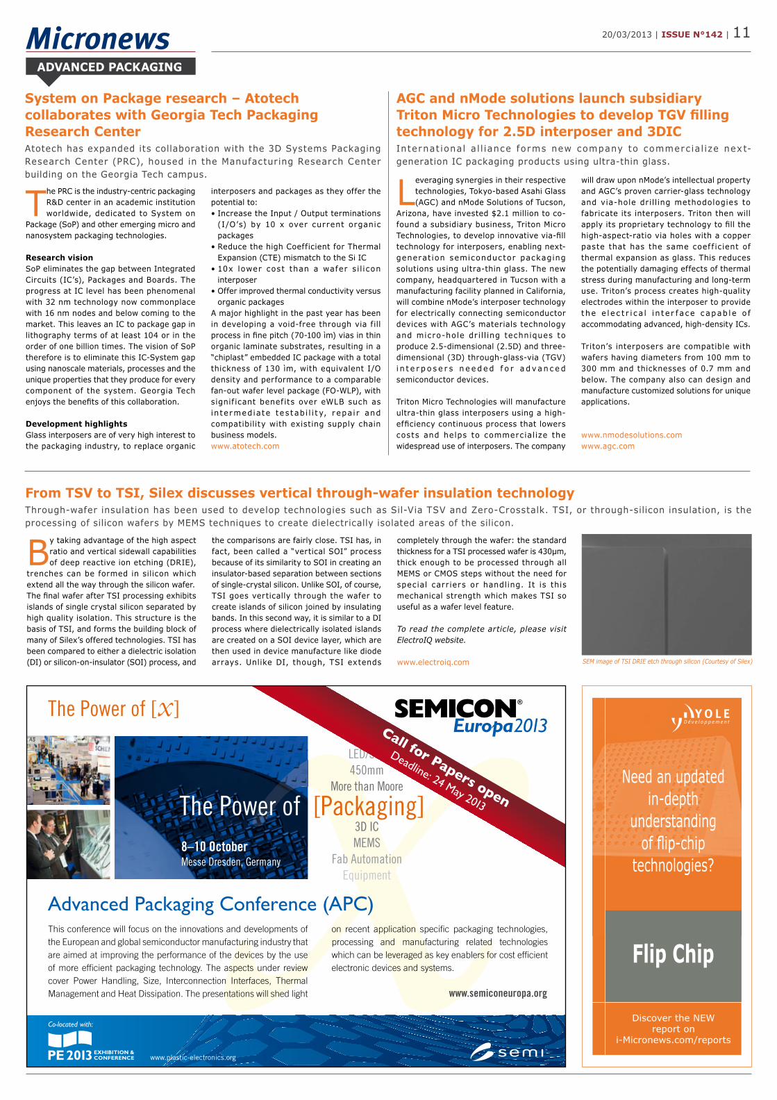
By taking advantage of the high aspect ratio and vertical sidewall capabilities of deep reactive ion etching (DRIE),
trenches can be formed in silicon which extend all the way through the silicon wafer.The fi nal wafer after TSI processing exhibits islands of single crystal silicon separated by high quality isolation. This structure is the basis of TSI, and forms the building block of many of Silex’s offered technologies. TSI has been compared to either a dielectric isolation (DI) or silicon-on-insulator (SOI) process, and
the comparisons are fairly close. TSI has, in fact, been called a “vertical SOI” process because of its similarity to SOI in creating an insulator-based separation between sections of single-crystal silicon. Unlike SOI, of course, TSI goes vertically through the wafer to create islands of silicon joined by insulating bands. In this second way, it is similar to a DI process where dielectrically isolated islands are created on a SOI device layer, which are then used in device manufacture like diode arrays. Unlike DI, though, TSI extends
completely through the wafer: the standard thickness for a TSI processed wafer is 430μm, thick enough to be processed through all MEMS or CMOS steps without the need for special carr iers or handling. It is this mechanical strength which makes TSI so useful as a wafer level feature.
To read the complete article, please visit ElectroIQ website. www.electroiq.com
From TSV to TSI, Silex discusses vertical through-wafer insulation technologyThrough-wafer insulation has been used to develop technologies such as Sil-Via TSV and Zero-Crosstalk. TSI, or through-silicon insulation, is the processing of silicon wafers by MEMS techniques to create dielectrically isolated areas of the silicon.
SEM image of TSI DRIE etch through silicon (Courtesy of Silex)
www.plastic-electronics.org
Co-located with:
The Power of [x]
This conference will focus on the innovations and developments of the European and global semiconductor manufacturing industry that are aimed at improving the performance of the devices by the use of more effi cient packaging technology. The aspects under review cover Power Handling, Size, Interconnection Interfaces, Thermal Management and Heat Dissipation. The presentations will shed light
The Power of [Packaging]
Advanced Packaging Conference (APC)
www.semiconeuropa.org
8–10 October Messe Dresden, Germany
on recent application specifi c packaging technologies, processing and manufacturing related technologies which can be leveraged as key enablers for cost effi cient electronic devices and systems.
EUVLED/SSL450mm
More than Moore
3D ICMEMS
Fab AutomationEquipment
Call for Papers open
Deadline: 24 May 2013

12 | ISSUE N°142 | 20/03/2013
• The fi rst effi cient PV power conditioner to operate at 50KHz
• Simultaneous achievement of a 40% reduction in inverter size and 98% effi ciency operation, a form and function benefit uniquely enabled by Transphorm’s EZ-GaNTM module technology
Transphorm’s patented, high-performance EZ-GaNTM module technology, combines low switching and conduction losses offering reduced energy loss of over 50% compared to conventional silicon based power conversion designs while simultaneously operating at higher frequency. “The partnership between Yaskawa, the world leader in inver ter solutions, and Transphorm, the world leader in GaN-based power conversion, has produced the world’s f irst high power GaN power converter,” said Umesh Mishra, CEO of Transphorm. “This is a disruptive first step which signals the broad adoption of GaN-based power conversion solutions.” “By teaming with Transphorm, Yaskawa is again the technology leader in introducing new technologies into the market place with tremendous benef its to customers and society” said Tatsuya Yamada, General Manager Environment&Energy Business Div. Dr ives Div is ion of Yaskawa E lec tr ic . Transphorm’s effi cient, compact, and easy-to-embed solutions simplify the design and manufacturing of a wide variety of electrical systems and devices, including power supplies and adapters, PV Inverters for solar panels, motor drives and power conversion for electric vehicles. Transphorm’s proprietary EZ-GaNTM
platform can reduce power system size, increase energy density and deliver high efficiencies across the grid. For customers looking for a low-risk roadmap to the next generation of power conversion technology, EZ-GaN TM prov ides a cos t-e f f ec t ive, customizable and easy-to-use solution ready for commercial scale.
www.transphormusa.com
For the second year, Yole Développement and Serma Technologies have joined forces to organize the Successful
Semiconductor Fabless conference, a unique European event dedicated to the fabless business model. This event takes place in Paris, from April 10 to 12.In the 1970’s, the semiconductor industry was vertically integrated. Most companies were IDMs with manufacturing, design, intellectual property (IP) and marketing activities. During this period, manufacturing technology evolution was strong and required new fabs, which directly increased capital expenditures. Companies desired an attractive Return on Invested Capital (ROIC), and to obtain it they developed a new, lower-investment business model by including manufacturing services in their portfolio. In the 1980’s, the first pure foundries emerged - and ten years later, the fabless business model was born. The rest, as they say, is history; according to GSA, in 2011 there were 1,800 fabless companies worldwide, covering a variety of sectors.At Yole Développement we’ve spent the last few years exploring the semiconductor fabless business model and its evolution, and in Q2 2013 we’ll release a report detailing our f indings. The report will cover several industrial sectors including MEMS, Advanced Packaging and Power Electronics.Along with our partner, Serma Technologies, we’ve created a unique European destination where professionals can share ideas about fabless business models and discuss business oppor tunit ies. If you’re interested in discovering the latest technology trends and exchanging information with key players, you won’t want to miss Successful Semiconductor Fabless 2013, in Paris April 10 - 12.In the Power Electronics field, the fabless business model is not as common compared to the MEMS industry. According to Yole Développement, $4B was generated by MEMS fabless companies in 2012, against less than $300K in the Power Electronics area. Is Power Electronics a world apart?“Less than 10 companies have been clearly identifi ed in the Power Electronics industry.
This trend is clearly linked to the introduction of new materials like GaN and SiC wafers in manufacturing technologies. New products already commerc ial ized, for example photovoltaic inver ters, use these new materials. Yole Développement is currently analyzing the Power Electronics industry in order to understand what the next step will be,” explains Alexandre Avron, Power Electronics Technology & Market Analyst at Yole Développement.Indeed, for a long time the Power Electronics field and its key players only considered silicon wafers. Today, however, the Power semiconductor industry is entering a new era: for the fi rst time, Power Electronics companies are developing new solutions based on “non-silicon” manufacturing technologies. This evolution is not without big investments, though, and in order to limit them, some companies have decided to become fabless and collaborate with large fabs to produce the necessary components.The truth is that Power Electronics is not a world apart, and that the fabless business model has just become a reality in the fi eld. It
represents a real opportunity for Power Electronics companies to introduce new components and embrace the technology evolution.
PROGRAMThe conference agenda includes presentations, panel discussions and networking over three exciting days.Key conference features include:- A comprehensive overview of the fabless
world- An understanding of the semiconductor
value chain and the fabless model’s current challenges
- A critical topics discussion: impact of current & future technologies, supply chain evolution and the fabless business model’s added-value
Key industry speakers: AptaSiC, Amkor Technology, ASE, CEA-LETI, CSEM, Delta Microelectronics, FEI Europe, GaN Systems, imec, Nanium, poLight, Serma Technologies and Yo l e Développement…To register, please visit www.ssf2013.frwww.ssf2013.fr
Transphorm enables the world’s first GaN-based high power converterFrom page 1
Is the Power Electronics industry a world apart?Discover the Successful Semiconductor Fabless 2013 conference on April 10 - 12 in Paris, France.
POWER ELECTRONICS
Key inverter applications and markets under
Yole Développement’s
scrutiny
Discover the NEWreport on
i-Micronews.com/reports
Inverter Technology
Trends & Market
Expectations
Semiconductor value chain deintegration:Business model’s historical evolution
(source: Successful Semiconductor Fabless conference, Yole Développement, Mar. 2013)
IDM*s are vertically integrated; In the 70’s, most companies were IDM.Foundries, focused on manufacturing, emerged in the 80’s.Fabless companies that outsourced manufacturing eventually became Foundries.Design house have emerged in the last decade; Their focus is on IP.
70’s80’s
90’s2000’s
IDM*
ManufacturingManufacturing
ManufacturingManufacturing
Design
DesignDesign
Design
Marketing
Intellectual
Property
Marketing
Intellectual
Property
Marketing
Intellectual
Property
Marketing
Intellectual
Property
FoundryFabless
Design House
*Integrated Devices Manufacturer

20/03/2013 | ISSUE N°142 | 13
YOLE IN THE PRESS TECHNOLOGY & MARKET REPORTS
What’s new compared to last edition?• Analysis of new UV LED applications• Update of all market metrics: UV lamps, UV systems,
UV LEDs, etc.• Update of all roadmaps (performance, price, etc.)• Highlight of 2012 UV LED trends (new technologies, etc.)• New players analysis across the supply chain
Key features• Detailed technical and market analysis of uV lamp and
UV LED applications• UV LED industry analysis: from substrate to system• UV lamp market metrics (units and value)• UV LED market metrics (value)• Emerging applications analysis
…In addition to traditional applications (UV lamps replacement), and due to their unique properties (compactness, higher lifetime, robustness, etc.), UV LEDs are also creating new applications that aren’t accessible to traditional UV lamps, i.e. apps that are miniaturized and portable. “In 2012, several new UV LED-based products were launched, including cell phone disinfection systems, nail gel curing systems and miniaturized counterfeit money detectors - and this is likely to continue!”, explains announced Pars Mukish, Technology & Market Analyst, LED, at Yole Développement. “We estimate that if new UV LED applications continue emerging, the associated business could represent nearly $30M by 2017, which would increase the overall UV LED market size to nearly $300M”, he adds…
Released in March 2013
Over the next fi ve years, an incredible 3x wafer growth is expected for the Flip-Chip platform, which will reach 40M+ of 12’’eq wspy by 2018!
Despite its high 19% CAGR, Flip-chip is not new - in fac t , i t was f i r s t introduced by IBM over 30 years ago!
As such, it would be easy to consider it an old, uninteresting, mature technology… but this is far from true! Instead, Flip-Chip is keeping up with the times and developing new bumping solutions to serve the most advanced technologies, like 3DIC and 2.5D.
Indeed, no matter what packaging technology you’re using, a bumping step is always required at the end! In 2012, bumping technologies accounted for 81% of the total installed capacity in the middle end area. That’s big. Really big. So big that it represents 14M+ 12’’eq wafers - and fab loading rates are high as well, especially for the Cu pillar platform (88%).
Flip-Chip is also big on value: in 2012 it was a $20B market (making it the biggest market i n t he m idd l e - end a r ea), and Yo l e Développement expects it to continue growing at an 9% clip, ultimately reaching $35B by 2018! …
Sources: Solid State Technology – EETimes Asia – Semiconductor Packaging News – Circuit Net – Pradeeps point – Global SMT – Design Reuse – Circuit Assembly – 3DInCities – tweetbuzz – Packaging Industry News…
Did you know?
More than 400 people registered to Yole Développement’s webcast dedicated to the Flip-Chip industry : “Flip Chip: An established platform still in mutation…” .
The webcas t i s s t i l l ava i lab le on www.i -mic r onews.com, A r ch ived Webcast section.
Feel free to register to view it.
2012 to 2017 UV LED market size (chip & package)Comparison of scenarios (Source: UV LEDs report, March 2013, Yole Développement)
Traditional UVlamp market
$309,4M87,3%
UV LEDmarket$45M12,7%
Traditional UVlamp market
$507M65,3%
UV LEDmarket
$269,1M34,7%
Discover Yole Développement two most recent reports. Detailed information about Yole Développement’s technology & market analysis is available on www.i-micronews.com, Reports section.
UV LED Technology & Application Trends ReportFrom $45M in 2012 to $270M in 2017, the UV LED market is booming - but we’re just scratching the surface of the technology’s true potential.
Cu pi l lar and micro-bumping for memory, consumer electronics and mobile phones have reinvigorated the Flip-Chip market, enabling it to grow at a 19% rate and cater to the most advanced technologies, like 3DIC and 2.5D.
What ’s new compared to 2011 edition:• Fully updated 2010 - 2018 market forecast and bottom-up
approach, including micro-bumping for 3DIC! • 2012 installed capacity / Comparison between C2 and TCB • Strong focus on micro-bumping for 3DIC & 2.5D • Market share/data for Flip-Chip bonder • Detailed technology roadmap • Application focus: HB-LED, CIS, μbumping for 3DIC and
2.5D, memory, analog, RF, mixed signals IC
Released in March 2013
Flip-Chip Market and Technology Trends Report
Simplified technological roadmap for FC BGA(Source: Flip Chip Market and Technology Trends Report, March 2013, Yole Développement)
0
20
40
60
80
100
120
140
160
2002 2004 2006 2008 2010 2012 2014 2016 2018
Pitc
h (
m)
Screen Printing
Electroplating
Electroplating / Evaporation / Stud bumping
Micro-bump bonding
Bump-less ‘pads’?
Powerful?…then you are right here!
The marketplace for developers and innovators.Future starts here!
International Exhibition and Conferencefor Power Electronics, Intelligent Motion,Renewable Energy and Energy ManagementNuremberg, 14 – 16 May 2013
More information at +49 711 [email protected] or pcim-europe.com
For information on our reports and specifi c market analysis services, please contact D. Jourdan ([email protected])