Embed Size (px)
Citation preview
This is information on a product in full production.
November 2016 DocID025056 Rev 5 1/52
LIS2DH12
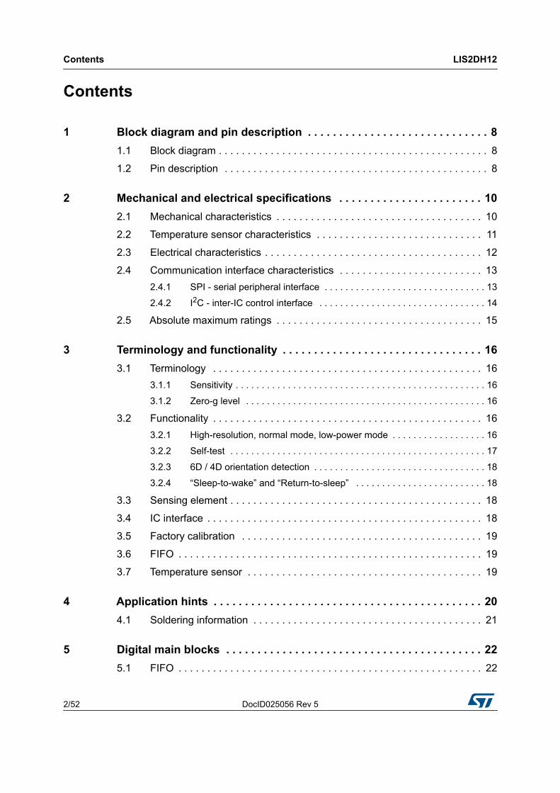
MEMS digital output motion sensor: ultra-low-power high-performance 3-axis "femto" accelerometer
Datasheet - production data
Features Wide supply voltage, 1.71 V to 3.6 V Independent IO supply (1.8 V) and supply
voltage compatible Ultra-low power consumption down to 2 μA 2g/±4g/8g/16g selectable full scales I2C/SPI digital output interface 2 independent programmable interrupt
generators for free-fall and motion detection 6D/4D orientation detection “Sleep-to-wake” and “return-to-sleep” functions Free-fall detection Motion detection Embedded temperature sensor Embedded FIFO ECOPACK®, RoHS and “Green” compliant
Applications Motion-activated functions Display orientation Shake control Pedometer Gaming and virtual reality input devices Impact recognition and logging
DescriptionThe LIS2DH12 is an ultra-low-power high-performance three-axis linear accelerometer belonging to the “femto” family with digital I2C/SPI serial interface standard output.
The LIS2DH12 has user-selectable full scales of 2g/±4g/8g/16g and is capable of measuring accelerations with output data rates from 1 Hz to 5.3 kHz.
The self-test capability allows the user to check the functionality of the sensor in the final application.
The device may be configured to generate interrupt signals by detecting two independent inertial wake-up/free-fall events as well as by the position of the device itself.
The LIS2DH12 is available in a small thin plastic land grid array package (LGA) and is guaranteed to operate over an extended temperature range from -40 °C to +85 °C.
Table 1. Device summary
Order code Temp. range [C] Package Packaging
LIS2DH12TR -40 to +85 LGA-12 Tape and reel
www.st.com
Contents LIS2DH12
2/52 DocID025056 Rev 5
Contents
1 Block diagram and pin description . . . . . . . . . . . . . . . . . . . . . . . . . . . . . 81.1 Block diagram . . . . . . . . . . . . . . . . . . . . . . . . . . . . . . . . . . . . . . . . . . . . . . . 8
1.2 Pin description . . . . . . . . . . . . . . . . . . . . . . . . . . . . . . . . . . . . . . . . . . . . . . 8
2 Mechanical and electrical specifications . . . . . . . . . . . . . . . . . . . . . . . 102.1 Mechanical characteristics . . . . . . . . . . . . . . . . . . . . . . . . . . . . . . . . . . . . 10
2.2 Temperature sensor characteristics . . . . . . . . . . . . . . . . . . . . . . . . . . . . . 11
2.3 Electrical characteristics . . . . . . . . . . . . . . . . . . . . . . . . . . . . . . . . . . . . . . 12
2.4 Communication interface characteristics . . . . . . . . . . . . . . . . . . . . . . . . . 132.4.1 SPI - serial peripheral interface . . . . . . . . . . . . . . . . . . . . . . . . . . . . . . . 13
2.4.2 I2C - inter-IC control interface . . . . . . . . . . . . . . . . . . . . . . . . . . . . . . . . 14
2.5 Absolute maximum ratings . . . . . . . . . . . . . . . . . . . . . . . . . . . . . . . . . . . . 15
3 Terminology and functionality . . . . . . . . . . . . . . . . . . . . . . . . . . . . . . . . 163.1 Terminology . . . . . . . . . . . . . . . . . . . . . . . . . . . . . . . . . . . . . . . . . . . . . . . 16
3.1.1 Sensitivity . . . . . . . . . . . . . . . . . . . . . . . . . . . . . . . . . . . . . . . . . . . . . . . . 16
3.1.2 Zero-g level . . . . . . . . . . . . . . . . . . . . . . . . . . . . . . . . . . . . . . . . . . . . . . 16
3.2 Functionality . . . . . . . . . . . . . . . . . . . . . . . . . . . . . . . . . . . . . . . . . . . . . . . 163.2.1 High-resolution, normal mode, low-power mode . . . . . . . . . . . . . . . . . . 16
3.2.2 Self-test . . . . . . . . . . . . . . . . . . . . . . . . . . . . . . . . . . . . . . . . . . . . . . . . . 17
3.2.3 6D / 4D orientation detection . . . . . . . . . . . . . . . . . . . . . . . . . . . . . . . . . 18
3.2.4 “Sleep-to-wake” and “Return-to-sleep” . . . . . . . . . . . . . . . . . . . . . . . . . 18
3.3 Sensing element . . . . . . . . . . . . . . . . . . . . . . . . . . . . . . . . . . . . . . . . . . . . 18
3.4 IC interface . . . . . . . . . . . . . . . . . . . . . . . . . . . . . . . . . . . . . . . . . . . . . . . . 18
3.5 Factory calibration . . . . . . . . . . . . . . . . . . . . . . . . . . . . . . . . . . . . . . . . . . 19
3.6 FIFO . . . . . . . . . . . . . . . . . . . . . . . . . . . . . . . . . . . . . . . . . . . . . . . . . . . . . 19
3.7 Temperature sensor . . . . . . . . . . . . . . . . . . . . . . . . . . . . . . . . . . . . . . . . . 19
4 Application hints . . . . . . . . . . . . . . . . . . . . . . . . . . . . . . . . . . . . . . . . . . . 204.1 Soldering information . . . . . . . . . . . . . . . . . . . . . . . . . . . . . . . . . . . . . . . . 21
5 Digital main blocks . . . . . . . . . . . . . . . . . . . . . . . . . . . . . . . . . . . . . . . . . 225.1 FIFO . . . . . . . . . . . . . . . . . . . . . . . . . . . . . . . . . . . . . . . . . . . . . . . . . . . . . 22
DocID025056 Rev 5 3/52
LIS2DH12 Contents
52
5.1.1 Bypass mode . . . . . . . . . . . . . . . . . . . . . . . . . . . . . . . . . . . . . . . . . . . . . 22
5.1.2 FIFO mode . . . . . . . . . . . . . . . . . . . . . . . . . . . . . . . . . . . . . . . . . . . . . . . 22
5.1.3 Stream mode . . . . . . . . . . . . . . . . . . . . . . . . . . . . . . . . . . . . . . . . . . . . . 23
5.1.4 Stream-to-FIFO mode . . . . . . . . . . . . . . . . . . . . . . . . . . . . . . . . . . . . . . 23
5.1.5 Retrieving data from FIFO . . . . . . . . . . . . . . . . . . . . . . . . . . . . . . . . . . . 23
6 Digital interfaces . . . . . . . . . . . . . . . . . . . . . . . . . . . . . . . . . . . . . . . . . . . 246.1 I2C serial interface . . . . . . . . . . . . . . . . . . . . . . . . . . . . . . . . . . . . . . . . . . 24
6.1.1 I2C operation . . . . . . . . . . . . . . . . . . . . . . . . . . . . . . . . . . . . . . . . . . . . . 25
6.2 SPI bus interface . . . . . . . . . . . . . . . . . . . . . . . . . . . . . . . . . . . . . . . . . . . 276.2.1 SPI read . . . . . . . . . . . . . . . . . . . . . . . . . . . . . . . . . . . . . . . . . . . . . . . . . 28
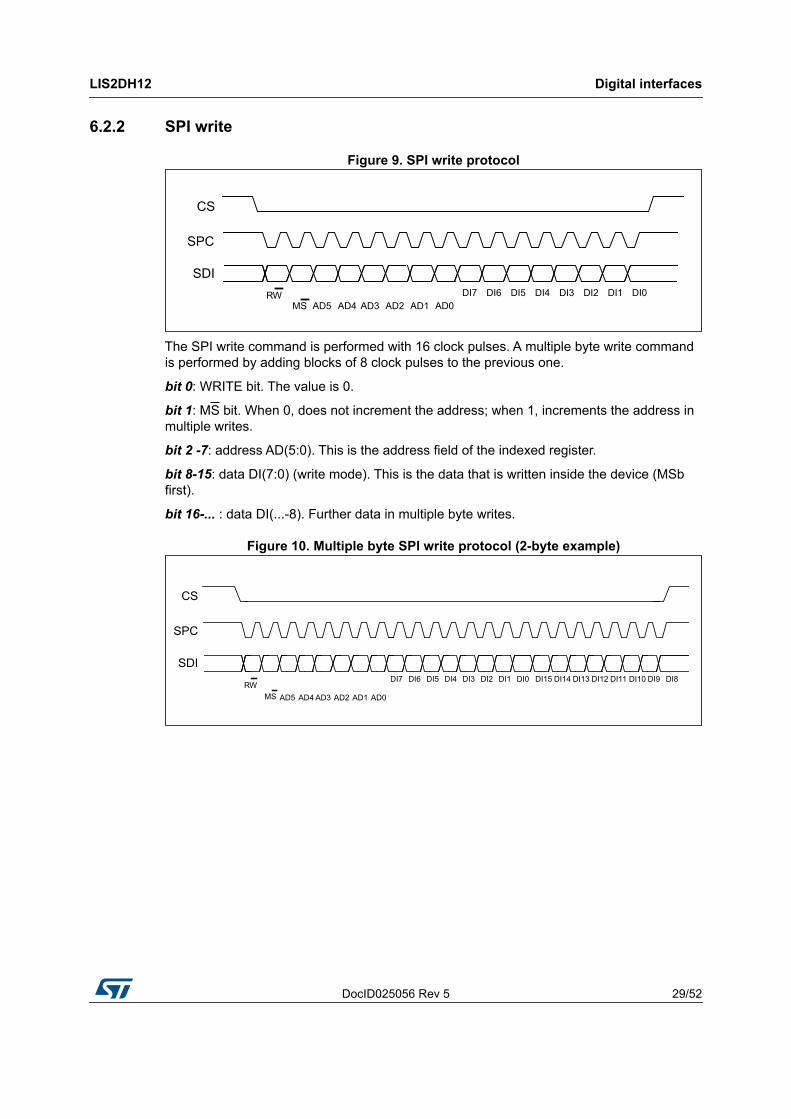
6.2.2 SPI write . . . . . . . . . . . . . . . . . . . . . . . . . . . . . . . . . . . . . . . . . . . . . . . . 29
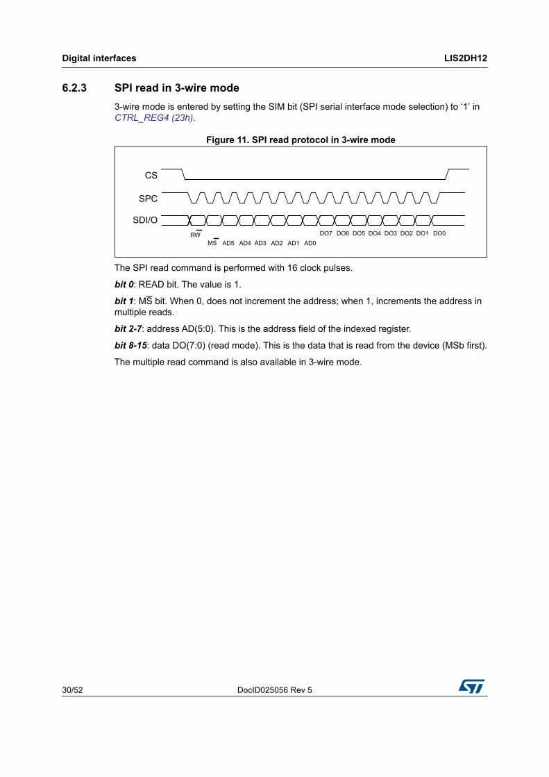
6.2.3 SPI read in 3-wire mode . . . . . . . . . . . . . . . . . . . . . . . . . . . . . . . . . . . . 30
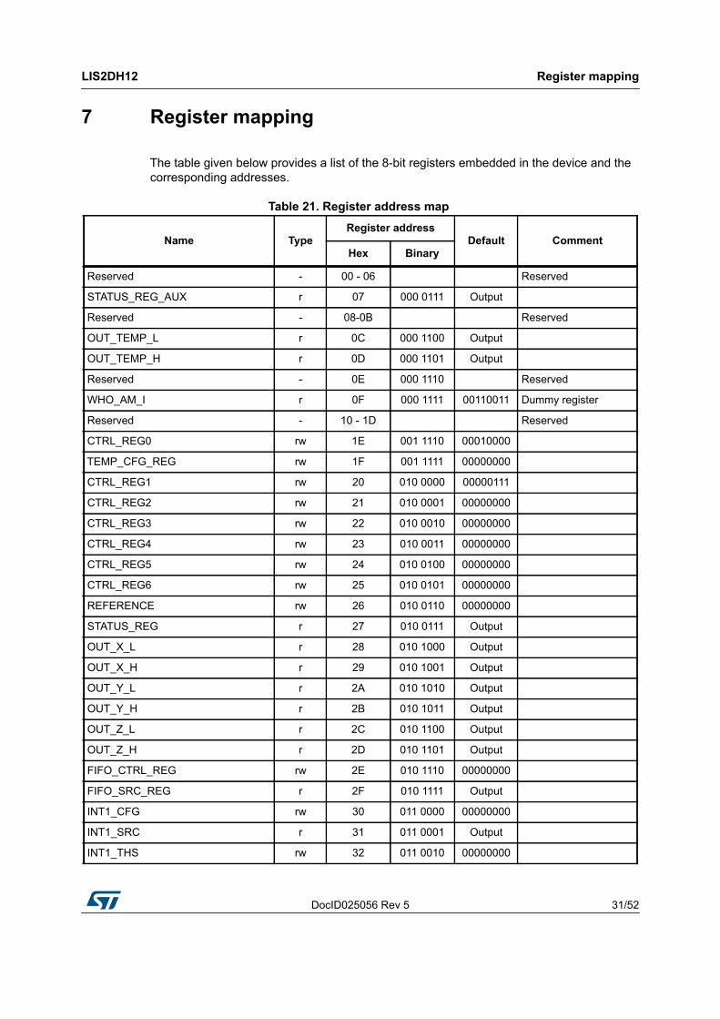
7 Register mapping . . . . . . . . . . . . . . . . . . . . . . . . . . . . . . . . . . . . . . . . . . 31
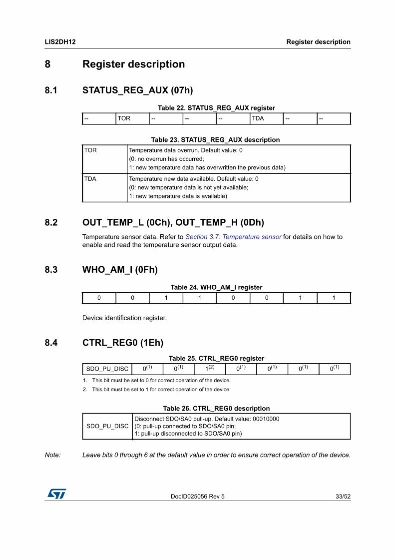
8 Register description . . . . . . . . . . . . . . . . . . . . . . . . . . . . . . . . . . . . . . . . 338.1 STATUS_REG_AUX (07h) . . . . . . . . . . . . . . . . . . . . . . . . . . . . . . . . . . . . 33
8.2 OUT_TEMP_L (0Ch), OUT_TEMP_H (0Dh) . . . . . . . . . . . . . . . . . . . . . . 33
8.3 WHO_AM_I (0Fh) . . . . . . . . . . . . . . . . . . . . . . . . . . . . . . . . . . . . . . . . . . . 33
8.4 CTRL_REG0 (1Eh) . . . . . . . . . . . . . . . . . . . . . . . . . . . . . . . . . . . . . . . . . 33
8.5 TEMP_CFG_REG (1Fh) . . . . . . . . . . . . . . . . . . . . . . . . . . . . . . . . . . . . . 34
8.6 CTRL_REG1 (20h) . . . . . . . . . . . . . . . . . . . . . . . . . . . . . . . . . . . . . . . . . . 34
8.7 CTRL_REG2 (21h) . . . . . . . . . . . . . . . . . . . . . . . . . . . . . . . . . . . . . . . . . . 35
8.8 CTRL_REG3 (22h) . . . . . . . . . . . . . . . . . . . . . . . . . . . . . . . . . . . . . . . . . . 35
8.9 CTRL_REG4 (23h) . . . . . . . . . . . . . . . . . . . . . . . . . . . . . . . . . . . . . . . . . . 36
8.10 CTRL_REG5 (24h) . . . . . . . . . . . . . . . . . . . . . . . . . . . . . . . . . . . . . . . . . . 37
8.11 CTRL_REG6 (25h) . . . . . . . . . . . . . . . . . . . . . . . . . . . . . . . . . . . . . . . . . . 37
8.12 REFERENCE (26h) . . . . . . . . . . . . . . . . . . . . . . . . . . . . . . . . . . . . . . . . . 38
8.13 STATUS_REG (27h) . . . . . . . . . . . . . . . . . . . . . . . . . . . . . . . . . . . . . . . . . 38
8.14 OUT_X_L (28h), OUT_X_H (29h) . . . . . . . . . . . . . . . . . . . . . . . . . . . . . . 39
8.15 OUT_Y_L (2Ah), OUT_Y_H (2Bh) . . . . . . . . . . . . . . . . . . . . . . . . . . . . . . 39
8.16 OUT_Z_L (2Ch), OUT_Z_H (2Dh) . . . . . . . . . . . . . . . . . . . . . . . . . . . . . . 39
8.17 FIFO_CTRL_REG (2Eh) . . . . . . . . . . . . . . . . . . . . . . . . . . . . . . . . . . . . . 39
8.18 FIFO_SRC_REG (2Fh) . . . . . . . . . . . . . . . . . . . . . . . . . . . . . . . . . . . . . . 40

Contents LIS2DH12
4/52 DocID025056 Rev 5
8.19 INT1_CFG (30h) . . . . . . . . . . . . . . . . . . . . . . . . . . . . . . . . . . . . . . . . . . . . 40
8.20 INT1_SRC (31h) . . . . . . . . . . . . . . . . . . . . . . . . . . . . . . . . . . . . . . . . . . . . 41
8.21 INT1_THS (32h) . . . . . . . . . . . . . . . . . . . . . . . . . . . . . . . . . . . . . . . . . . . . 42
8.22 INT1_DURATION (33h) . . . . . . . . . . . . . . . . . . . . . . . . . . . . . . . . . . . . . . 42
8.23 INT2_CFG (34h) . . . . . . . . . . . . . . . . . . . . . . . . . . . . . . . . . . . . . . . . . . . . 43
8.24 INT2_SRC (35h) . . . . . . . . . . . . . . . . . . . . . . . . . . . . . . . . . . . . . . . . . . . . 44
8.25 INT2_THS (36h) . . . . . . . . . . . . . . . . . . . . . . . . . . . . . . . . . . . . . . . . . . . . 44
8.26 INT2_DURATION (37h) . . . . . . . . . . . . . . . . . . . . . . . . . . . . . . . . . . . . . . 45
8.27 CLICK_CFG (38h) . . . . . . . . . . . . . . . . . . . . . . . . . . . . . . . . . . . . . . . . . . 45
8.28 CLICK_SRC (39h) . . . . . . . . . . . . . . . . . . . . . . . . . . . . . . . . . . . . . . . . . . 46
8.29 CLICK_THS (3Ah) . . . . . . . . . . . . . . . . . . . . . . . . . . . . . . . . . . . . . . . . . . 46
8.30 TIME_LIMIT (3Bh) . . . . . . . . . . . . . . . . . . . . . . . . . . . . . . . . . . . . . . . . . . 46
8.31 TIME_LATENCY (3Ch) . . . . . . . . . . . . . . . . . . . . . . . . . . . . . . . . . . . . . . . 47
8.32 TIME_WINDOW (3Dh) . . . . . . . . . . . . . . . . . . . . . . . . . . . . . . . . . . . . . . . 47
8.33 ACT_THS (3Eh) . . . . . . . . . . . . . . . . . . . . . . . . . . . . . . . . . . . . . . . . . . . . 47
8.34 ACT_DUR (3Fh) . . . . . . . . . . . . . . . . . . . . . . . . . . . . . . . . . . . . . . . . . . . . 47
9 Package information . . . . . . . . . . . . . . . . . . . . . . . . . . . . . . . . . . . . . . . . 489.1 LGA-12 package information . . . . . . . . . . . . . . . . . . . . . . . . . . . . . . . . . . 48
9.2 LGA-12 packing information . . . . . . . . . . . . . . . . . . . . . . . . . . . . . . . . . . . 49
10 Revision history . . . . . . . . . . . . . . . . . . . . . . . . . . . . . . . . . . . . . . . . . . . 51
DocID025056 Rev 5 5/52
LIS2DH12 List of tables
52
List of tables
Table 1. Device summary . . . . . . . . . . . . . . . . . . . . . . . . . . . . . . . . . . . . . . . . . . . . . . . . . . . . . . . . . . 1Table 2. Pin description . . . . . . . . . . . . . . . . . . . . . . . . . . . . . . . . . . . . . . . . . . . . . . . . . . . . . . . . . . . 9Table 3. Internal pull-up values (typ.) for SDO/SA0 pin . . . . . . . . . . . . . . . . . . . . . . . . . . . . . . . . . . . 9Table 4. Mechanical characteristics . . . . . . . . . . . . . . . . . . . . . . . . . . . . . . . . . . . . . . . . . . . . . . . . . 10Table 5. Temperature sensor characteristics . . . . . . . . . . . . . . . . . . . . . . . . . . . . . . . . . . . . . . . . . . 11Table 6. Electrical characteristics . . . . . . . . . . . . . . . . . . . . . . . . . . . . . . . . . . . . . . . . . . . . . . . . . . . 12Table 7. SPI slave timing values. . . . . . . . . . . . . . . . . . . . . . . . . . . . . . . . . . . . . . . . . . . . . . . . . . . . 13Table 8. I2C slave timing values . . . . . . . . . . . . . . . . . . . . . . . . . . . . . . . . . . . . . . . . . . . . . . . . . . . . 14Table 9. Absolute maximum ratings . . . . . . . . . . . . . . . . . . . . . . . . . . . . . . . . . . . . . . . . . . . . . . . . . 15Table 10. Operating mode selection. . . . . . . . . . . . . . . . . . . . . . . . . . . . . . . . . . . . . . . . . . . . . . . . . . 16Table 11. Turn-on time for operating mode transition. . . . . . . . . . . . . . . . . . . . . . . . . . . . . . . . . . . . . 17Table 12. Current consumption of operating modes. . . . . . . . . . . . . . . . . . . . . . . . . . . . . . . . . . . . . . 17Table 13. Internal pin status . . . . . . . . . . . . . . . . . . . . . . . . . . . . . . . . . . . . . . . . . . . . . . . . . . . . . . . . 21Table 14. Serial interface pin description . . . . . . . . . . . . . . . . . . . . . . . . . . . . . . . . . . . . . . . . . . . . . . 24Table 15. I2C terminology . . . . . . . . . . . . . . . . . . . . . . . . . . . . . . . . . . . . . . . . . . . . . . . . . . . . . . . . . . 24Table 16. SAD+read/write patterns. . . . . . . . . . . . . . . . . . . . . . . . . . . . . . . . . . . . . . . . . . . . . . . . . . . 25Table 17. Transfer when master is writing one byte to slave . . . . . . . . . . . . . . . . . . . . . . . . . . . . . . . 25Table 18. Transfer when master is writing multiple bytes to slave . . . . . . . . . . . . . . . . . . . . . . . . . . . 26Table 19. Transfer when master is receiving (reading) one byte of data from slave . . . . . . . . . . . . . 26Table 20. Transfer when master is receiving (reading) multiple bytes of data from slave . . . . . . . . . 26Table 21. Register address map. . . . . . . . . . . . . . . . . . . . . . . . . . . . . . . . . . . . . . . . . . . . . . . . . . . . . 31Table 22. STATUS_REG_AUX register . . . . . . . . . . . . . . . . . . . . . . . . . . . . . . . . . . . . . . . . . . . . . . . 33Table 23. STATUS_REG_AUX description . . . . . . . . . . . . . . . . . . . . . . . . . . . . . . . . . . . . . . . . . . . . 33Table 24. WHO_AM_I register . . . . . . . . . . . . . . . . . . . . . . . . . . . . . . . . . . . . . . . . . . . . . . . . . . . . . . 33Table 25. CTRL_REG0 register . . . . . . . . . . . . . . . . . . . . . . . . . . . . . . . . . . . . . . . . . . . . . . . . . . . . . 33Table 26. CTRL_REG0 description . . . . . . . . . . . . . . . . . . . . . . . . . . . . . . . . . . . . . . . . . . . . . . . . . . 33Table 27. TEMP_CFG_REG register . . . . . . . . . . . . . . . . . . . . . . . . . . . . . . . . . . . . . . . . . . . . . . . . . 34Table 28. TEMP_CFG_REG description . . . . . . . . . . . . . . . . . . . . . . . . . . . . . . . . . . . . . . . . . . . . . . 34Table 29. CTRL_REG1 register . . . . . . . . . . . . . . . . . . . . . . . . . . . . . . . . . . . . . . . . . . . . . . . . . . . . . 34Table 30. CTRL_REG1 description . . . . . . . . . . . . . . . . . . . . . . . . . . . . . . . . . . . . . . . . . . . . . . . . . . 34Table 31. Data rate configuration . . . . . . . . . . . . . . . . . . . . . . . . . . . . . . . . . . . . . . . . . . . . . . . . . . . . 34Table 32. CTRL_REG2 register . . . . . . . . . . . . . . . . . . . . . . . . . . . . . . . . . . . . . . . . . . . . . . . . . . . . . 35Table 33. CTRL_REG2 description . . . . . . . . . . . . . . . . . . . . . . . . . . . . . . . . . . . . . . . . . . . . . . . . . . 35Table 34. High-pass filter mode configuration . . . . . . . . . . . . . . . . . . . . . . . . . . . . . . . . . . . . . . . . . . 35Table 35. CTRL_REG3 register . . . . . . . . . . . . . . . . . . . . . . . . . . . . . . . . . . . . . . . . . . . . . . . . . . . . . 35Table 36. CTRL_REG3 description . . . . . . . . . . . . . . . . . . . . . . . . . . . . . . . . . . . . . . . . . . . . . . . . . . 35Table 37. CTRL_REG4 register . . . . . . . . . . . . . . . . . . . . . . . . . . . . . . . . . . . . . . . . . . . . . . . . . . . . . 36Table 38. CTRL_REG4 description . . . . . . . . . . . . . . . . . . . . . . . . . . . . . . . . . . . . . . . . . . . . . . . . . . 36Table 39. Self-test mode configuration . . . . . . . . . . . . . . . . . . . . . . . . . . . . . . . . . . . . . . . . . . . . . . . . 36Table 40. CTRL_REG5 register . . . . . . . . . . . . . . . . . . . . . . . . . . . . . . . . . . . . . . . . . . . . . . . . . . . . . 37Table 41. CTRL_REG5 description . . . . . . . . . . . . . . . . . . . . . . . . . . . . . . . . . . . . . . . . . . . . . . . . . . 37Table 42. CTRL_REG6 register . . . . . . . . . . . . . . . . . . . . . . . . . . . . . . . . . . . . . . . . . . . . . . . . . . . . . 37Table 43. CTRL_REG6 description . . . . . . . . . . . . . . . . . . . . . . . . . . . . . . . . . . . . . . . . . . . . . . . . . . 37Table 44. REFERENCE register. . . . . . . . . . . . . . . . . . . . . . . . . . . . . . . . . . . . . . . . . . . . . . . . . . . . . 38Table 45. REFERENCE description . . . . . . . . . . . . . . . . . . . . . . . . . . . . . . . . . . . . . . . . . . . . . . . . . . 38Table 46. STATUS_REG register . . . . . . . . . . . . . . . . . . . . . . . . . . . . . . . . . . . . . . . . . . . . . . . . . . . . 38Table 47. STATUS_REG description . . . . . . . . . . . . . . . . . . . . . . . . . . . . . . . . . . . . . . . . . . . . . . . . . 38Table 48. FIFO_CTRL_REG register . . . . . . . . . . . . . . . . . . . . . . . . . . . . . . . . . . . . . . . . . . . . . . . . . 39
List of tables LIS2DH12
6/52 DocID025056 Rev 5
Table 49. FIFO_CTRL_REG description . . . . . . . . . . . . . . . . . . . . . . . . . . . . . . . . . . . . . . . . . . . . . . 39Table 50. FIFO mode configuration . . . . . . . . . . . . . . . . . . . . . . . . . . . . . . . . . . . . . . . . . . . . . . . . . . 39Table 51. FIFO_SRC_REG register . . . . . . . . . . . . . . . . . . . . . . . . . . . . . . . . . . . . . . . . . . . . . . . . . . 40Table 52. FIFO_SRC_REG description . . . . . . . . . . . . . . . . . . . . . . . . . . . . . . . . . . . . . . . . . . . . . . . 40Table 53. INT1_CFG register . . . . . . . . . . . . . . . . . . . . . . . . . . . . . . . . . . . . . . . . . . . . . . . . . . . . . . . 40Table 54. INT1_CFG description . . . . . . . . . . . . . . . . . . . . . . . . . . . . . . . . . . . . . . . . . . . . . . . . . . . . 40Table 55. Interrupt mode . . . . . . . . . . . . . . . . . . . . . . . . . . . . . . . . . . . . . . . . . . . . . . . . . . . . . . . . . . 41Table 56. INT1_SRC register . . . . . . . . . . . . . . . . . . . . . . . . . . . . . . . . . . . . . . . . . . . . . . . . . . . . . . . 41Table 57. INT1_SRC description . . . . . . . . . . . . . . . . . . . . . . . . . . . . . . . . . . . . . . . . . . . . . . . . . . . . 41Table 58. INT1_THS register . . . . . . . . . . . . . . . . . . . . . . . . . . . . . . . . . . . . . . . . . . . . . . . . . . . . . . . 42Table 59. INT1_THS description. . . . . . . . . . . . . . . . . . . . . . . . . . . . . . . . . . . . . . . . . . . . . . . . . . . . . 42Table 60. INT1_DURATION register . . . . . . . . . . . . . . . . . . . . . . . . . . . . . . . . . . . . . . . . . . . . . . . . . 42Table 61. INT1_DURATION description. . . . . . . . . . . . . . . . . . . . . . . . . . . . . . . . . . . . . . . . . . . . . . . 42Table 62. INT2_CFG register . . . . . . . . . . . . . . . . . . . . . . . . . . . . . . . . . . . . . . . . . . . . . . . . . . . . . . . 43Table 63. INT2_CFG description . . . . . . . . . . . . . . . . . . . . . . . . . . . . . . . . . . . . . . . . . . . . . . . . . . . . 43Table 64. Interrupt mode . . . . . . . . . . . . . . . . . . . . . . . . . . . . . . . . . . . . . . . . . . . . . . . . . . . . . . . . . . 43Table 65. INT2_SRC register . . . . . . . . . . . . . . . . . . . . . . . . . . . . . . . . . . . . . . . . . . . . . . . . . . . . . . . 44Table 66. INT2_SRC description . . . . . . . . . . . . . . . . . . . . . . . . . . . . . . . . . . . . . . . . . . . . . . . . . . . . 44Table 67. INT2_THS register . . . . . . . . . . . . . . . . . . . . . . . . . . . . . . . . . . . . . . . . . . . . . . . . . . . . . . . 44Table 68. INT2_THS description. . . . . . . . . . . . . . . . . . . . . . . . . . . . . . . . . . . . . . . . . . . . . . . . . . . . . 44Table 69. INT2_DURATION register . . . . . . . . . . . . . . . . . . . . . . . . . . . . . . . . . . . . . . . . . . . . . . . . . 45Table 70. INT2_DURATION description. . . . . . . . . . . . . . . . . . . . . . . . . . . . . . . . . . . . . . . . . . . . . . . 45Table 71. CLICK_CFG register. . . . . . . . . . . . . . . . . . . . . . . . . . . . . . . . . . . . . . . . . . . . . . . . . . . . . . 45Table 72. CLICK_CFG description . . . . . . . . . . . . . . . . . . . . . . . . . . . . . . . . . . . . . . . . . . . . . . . . . . . 45Table 73. CLICK_SRC register. . . . . . . . . . . . . . . . . . . . . . . . . . . . . . . . . . . . . . . . . . . . . . . . . . . . . . 46Table 74. CLICK_SRC description . . . . . . . . . . . . . . . . . . . . . . . . . . . . . . . . . . . . . . . . . . . . . . . . . . . 46Table 75. CLICK_THS register . . . . . . . . . . . . . . . . . . . . . . . . . . . . . . . . . . . . . . . . . . . . . . . . . . . . . . 46Table 76. CLICK_THS register description. . . . . . . . . . . . . . . . . . . . . . . . . . . . . . . . . . . . . . . . . . . . . 46Table 77. TIME_LIMIT register . . . . . . . . . . . . . . . . . . . . . . . . . . . . . . . . . . . . . . . . . . . . . . . . . . . . . . 46Table 78. TIME_LIMIT description . . . . . . . . . . . . . . . . . . . . . . . . . . . . . . . . . . . . . . . . . . . . . . . . . . . 46Table 79. TIME_LATENCY register . . . . . . . . . . . . . . . . . . . . . . . . . . . . . . . . . . . . . . . . . . . . . . . . . . 47Table 80. TIME_LATENCY description . . . . . . . . . . . . . . . . . . . . . . . . . . . . . . . . . . . . . . . . . . . . . . . 47Table 81. TIME_WINDOW register. . . . . . . . . . . . . . . . . . . . . . . . . . . . . . . . . . . . . . . . . . . . . . . . . . . 47Table 82. TIME_WINDOW description . . . . . . . . . . . . . . . . . . . . . . . . . . . . . . . . . . . . . . . . . . . . . . . . 47Table 83. ACT_THS register. . . . . . . . . . . . . . . . . . . . . . . . . . . . . . . . . . . . . . . . . . . . . . . . . . . . . . . . 47Table 84. ACT_THS description . . . . . . . . . . . . . . . . . . . . . . . . . . . . . . . . . . . . . . . . . . . . . . . . . . . . . 47Table 85. ACT_DUR register . . . . . . . . . . . . . . . . . . . . . . . . . . . . . . . . . . . . . . . . . . . . . . . . . . . . . . . 47Table 86. ACT_DUR description. . . . . . . . . . . . . . . . . . . . . . . . . . . . . . . . . . . . . . . . . . . . . . . . . . . . . 47Table 87. Reel dimensions for carrier tape of LGA-12 package. . . . . . . . . . . . . . . . . . . . . . . . . . . . . 50Table 88. Document revision history. . . . . . . . . . . . . . . . . . . . . . . . . . . . . . . . . . . . . . . . . . . . . . . . . . 51
DocID025056 Rev 5 7/52
LIS2DH12 List of figures
52
List of figures
Figure 1. Block diagram . . . . . . . . . . . . . . . . . . . . . . . . . . . . . . . . . . . . . . . . . . . . . . . . . . . . . . . . . . . . 8Figure 2. Pin connections . . . . . . . . . . . . . . . . . . . . . . . . . . . . . . . . . . . . . . . . . . . . . . . . . . . . . . . . . . 8Figure 3. SPI slave timing diagram . . . . . . . . . . . . . . . . . . . . . . . . . . . . . . . . . . . . . . . . . . . . . . . . . . 13Figure 4. I2C slave timing diagram . . . . . . . . . . . . . . . . . . . . . . . . . . . . . . . . . . . . . . . . . . . . . . . . . . 14Figure 5. LIS2DH12 electrical connections . . . . . . . . . . . . . . . . . . . . . . . . . . . . . . . . . . . . . . . . . . . . 20Figure 6. Read and write protocol . . . . . . . . . . . . . . . . . . . . . . . . . . . . . . . . . . . . . . . . . . . . . . . . . . . 27Figure 7. SPI read protocol . . . . . . . . . . . . . . . . . . . . . . . . . . . . . . . . . . . . . . . . . . . . . . . . . . . . . . . . 28Figure 8. Multiple byte SPI read protocol (2-byte example) . . . . . . . . . . . . . . . . . . . . . . . . . . . . . . . . 28Figure 9. SPI write protocol . . . . . . . . . . . . . . . . . . . . . . . . . . . . . . . . . . . . . . . . . . . . . . . . . . . . . . . . 29Figure 10. Multiple byte SPI write protocol (2-byte example). . . . . . . . . . . . . . . . . . . . . . . . . . . . . . . . 29Figure 11. SPI read protocol in 3-wire mode . . . . . . . . . . . . . . . . . . . . . . . . . . . . . . . . . . . . . . . . . . . . 30Figure 12. LGA-12: package outline and mechanical data . . . . . . . . . . . . . . . . . . . . . . . . . . . . . . . . . 48Figure 13. Carrier tape information for LGA-12 package. . . . . . . . . . . . . . . . . . . . . . . . . . . . . . . . . . . 49Figure 14. LGA-12 package orientation in carrier tape . . . . . . . . . . . . . . . . . . . . . . . . . . . . . . . . . . . . 49Figure 15. Reel information for carrier tape of LGA-12 package . . . . . . . . . . . . . . . . . . . . . . . . . . . . . 50
Block diagram and pin description LIS2DH12
8/52 DocID025056 Rev 5
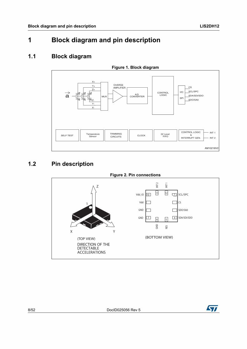
1 Block diagram and pin description
1.1 Block diagram
Figure 1. Block diagram
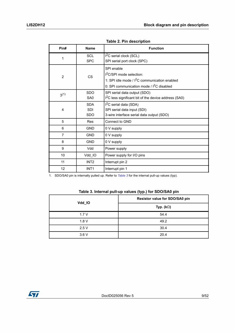
1.2 Pin description
Figure 2. Pin connections
CHARGEAMPLIFIER
Y+
Z+
Y-
Z-
a
X+
X-
I2C
SPI
CS
SCL/SPC
SDA/SDI/SDO
SDO/SA0
CONTROL LOGIC&
INTERRUPT GEN.
INT 1 CLOCK
TRIMMINGCIRCUITS
TemperatureSELF TEST
CONTROL A/D
CONVERTER
INT 2
MUX
32 Level FIFO
LOGIC
Sensor
AM10218V2
(TOP VIEW)
DIRECTION OF THEDETECTABLEACCELERATIONS
Y
1
X
Z
Vdd_
IO
SCL/SPC
SDA/SDI/SDO
CS
SDO/SA0
RES
GND
INT1
INT2
RES
Vdd
RES
(BOTTOM VIEW)
Pin 1 indicator
4
1
57
11
8
RES
RES
12 14
GND
SCL/SPC
SDA/SDI/SDO
CS
SDO/SA0GND
RES
INT1
Vdd_IO
(BOTTOM VIEW)
4
1
56GND
11
INT2
7
10
Vdd
12
DocID025056 Rev 5 9/52
LIS2DH12 Block diagram and pin description
52
Table 2. Pin description Pin# Name Function
1SCLSPC
I2C serial clock (SCL)SPI serial port clock (SPC)
2 CS
SPI enable
I2C/SPI mode selection:
1: SPI idle mode / I2C communication enabled
0: SPI communication mode / I2C disabled
3(1)
1. SDO/SA0 pin is internally pulled up. Refer to Table 3 for the internal pull-up values (typ).
SDOSA0
SPI serial data output (SDO)I2C less significant bit of the device address (SA0)
4SDASDISDO
I2C serial data (SDA)SPI serial data input (SDI)3-wire interface serial data output (SDO)
5 Res Connect to GND
6 GND 0 V supply
7 GND 0 V supply
8 GND 0 V supply
9 Vdd Power supply
10 Vdd_IO Power supply for I/O pins
11 INT2 Interrupt pin 2
12 INT1 Interrupt pin 1
Table 3. Internal pull-up values (typ.) for SDO/SA0 pin
Vdd_IOResistor value for SDO/SA0 pin
Typ. (kΩ)
1.7 V 54.4
1.8 V 49.2
2.5 V 30.4
3.6 V 20.4
Mechanical and electrical specifications LIS2DH12
10/52 DocID025056 Rev 5
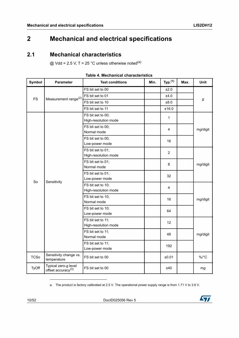
2 Mechanical and electrical specifications
2.1 Mechanical characteristics@ Vdd = 2.5 V, T = 25 °C unless otherwise noted(a)
a. The product is factory calibrated at 2.5 V. The operational power supply range is from 1.71 V to 3.6 V.
Table 4. Mechanical characteristics Symbol Parameter Test conditions Min. Typ.(1) Max. Unit
FS Measurement range(2)
FS bit set to 00 ±2.0
gFS bit set to 01 ±4.0
FS bit set to 10 ±8.0
FS bit set to 11 ±16.0
So Sensitivity
FS bit set to 00; High-resolution mode
1
mg/digitFS bit set to 00; Normal mode
4
FS bit set to 00; Low-power mode
16
FS bit set to 01;High-resolution mode
2
mg/digitFS bit set to 01;Normal mode
8
FS bit set to 01;Low-power mode
32
FS bit set to 10;High-resolution mode
4
mg/digitFS bit set to 10;Normal mode
16
FS bit set to 10;Low-power mode
64
FS bit set to 11;High-resolution mode
12
mg/digitFS bit set to 11;Normal mode
48
FS bit set to 11;Low-power mode
192
TCSo Sensitivity change vs. temperature FS bit set to 00 ±0.01 %/°C
TyOff Typical zero-g level offset accuracy(3) FS bit set to 00 ±40 mg
DocID025056 Rev 5 11/52
LIS2DH12 Mechanical and electrical specifications
52
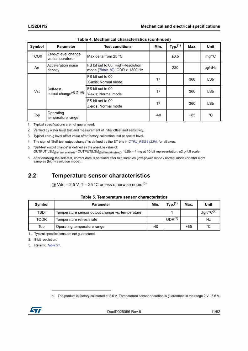
2.2 Temperature sensor characteristics@ Vdd = 2.5 V, T = 25 °C unless otherwise noted(b)
TCOff Zero-g level change vs. temperature Max delta from 25 °C ±0.5 mg/°C
An Acceleration noise density
FS bit set to 00, High-Resolution mode (Table 10), ODR > 1300 Hz 220 μg/√Hz
Vst Self-test output change(4) (5) (6)
FS bit set to 00X-axis; Normal mode
17 360 LSb
FS bit set to 00Y-axis; Normal mode
17 360 LSb
FS bit set to 00Z-axis; Normal mode
17 360 LSb
Top Operating temperature range -40 +85 °C
1. Typical specifications are not guaranteed.
2. Verified by wafer level test and measurement of initial offset and sensitivity.
3. Typical zero-g level offset value after factory calibration test at socket level.
4. The sign of “Self-test output change” is defined by the ST bits in CTRL_REG4 (23h), for all axes.
5. “Self-test output change” is defined as the absolute value of:OUTPUT[LSb](Self test enabled) - OUTPUT[LSb](Self test disabled). 1LSb = 4 mg at 10-bit representation, ±2 g full scale
6. After enabling the self-test, correct data is obtained after two samples (low-power mode / normal mode) or after eight samples (high-resolution mode).
Table 4. Mechanical characteristics (continued)Symbol Parameter Test conditions Min. Typ.(1) Max. Unit
b. The product is factory calibrated at 2.5 V. Temperature sensor operation is guaranteed in the range 2 V - 3.6 V.
Table 5. Temperature sensor characteristicsSymbol Parameter Min. Typ.(1) Max. Unit
TSDr Temperature sensor output change vs. temperature 1 digit/°C(2)
TODR Temperature refresh rate ODR(3) Hz
Top Operating temperature range -40 +85 °C
1. Typical specifications are not guaranteed.
2. 8-bit resolution.
3. Refer to Table 31.
Mechanical and electrical specifications LIS2DH12
12/52 DocID025056 Rev 5
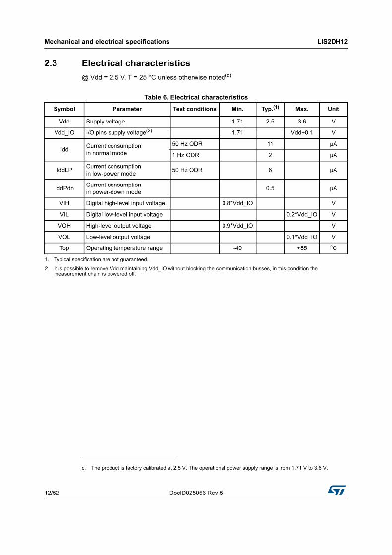
2.3 Electrical characteristics@ Vdd = 2.5 V, T = 25 °C unless otherwise noted(c)
c. The product is factory calibrated at 2.5 V. The operational power supply range is from 1.71 V to 3.6 V.
Table 6. Electrical characteristicsSymbol Parameter Test conditions Min. Typ.(1) Max. Unit
Vdd Supply voltage 1.71 2.5 3.6 V
Vdd_IO I/O pins supply voltage(2) 1.71 Vdd+0.1 V
Idd Current consumptionin normal mode
50 Hz ODR 11 μA
1 Hz ODR 2 μA
IddLP Current consumptionin low-power mode 50 Hz ODR 6 μA
IddPdn Current consumption in power-down mode 0.5 μA
VIH Digital high-level input voltage 0.8*Vdd_IO V
VIL Digital low-level input voltage 0.2*Vdd_IO V
VOH High-level output voltage 0.9*Vdd_IO V
VOL Low-level output voltage 0.1*Vdd_IO V
Top Operating temperature range -40 +85 °C
1. Typical specification are not guaranteed.
2. It is possible to remove Vdd maintaining Vdd_IO without blocking the communication busses, in this condition the measurement chain is powered off.
DocID025056 Rev 5 13/52
LIS2DH12 Mechanical and electrical specifications
52
2.4 Communication interface characteristics
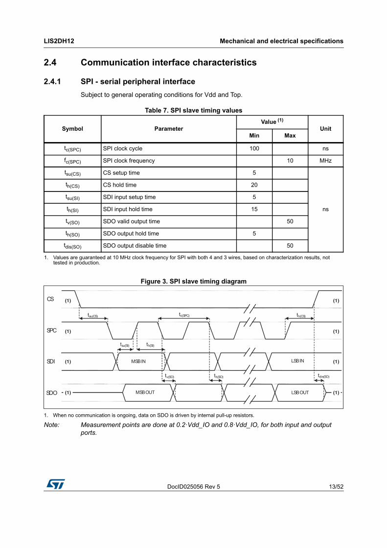
2.4.1 SPI - serial peripheral interfaceSubject to general operating conditions for Vdd and Top.
Figure 3. SPI slave timing diagram
1. When no communication is ongoing, data on SDO is driven by internal pull-up resistors.
Note: Measurement points are done at 0.2·Vdd_IO and 0.8·Vdd_IO, for both input and output ports.
Table 7. SPI slave timing values
Symbol ParameterValue (1)
UnitMin Max
tc(SPC) SPI clock cycle 100 ns
fc(SPC) SPI clock frequency 10 MHz
tsu(CS) CS setup time 5
ns
th(CS) CS hold time 20
tsu(SI) SDI input setup time 5
th(SI) SDI input hold time 15
tv(SO) SDO valid output time 50
th(SO) SDO output hold time 5
tdis(SO) SDO output disable time 50
1. Values are guaranteed at 10 MHz clock frequency for SPI with both 4 and 3 wires, based on characterization results, not tested in production.
SPC
CS
SDI
SDO
tsu(CS)
tv(SO) th(SO)
th(SI)tsu(SI)
th(CS)
tdis(SO)
tc(SPC)
MSB IN
MSB OUT LSB OUT
LSB IN
(1)
(1)
(1)
(1)
(1)
(1)
(1)
(1)
Mechanical and electrical specifications LIS2DH12
14/52 DocID025056 Rev 5
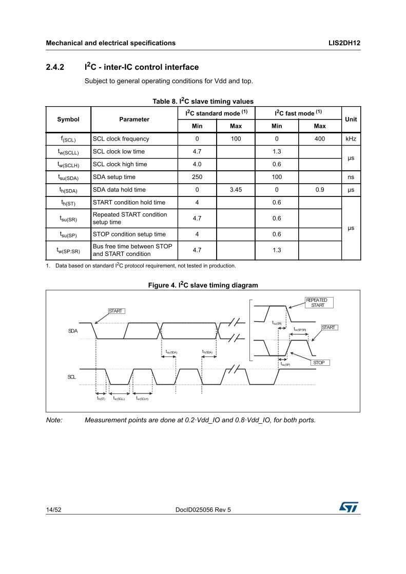
2.4.2 I2C - inter-IC control interfaceSubject to general operating conditions for Vdd and top.
Figure 4. I2C slave timing diagram
Note: Measurement points are done at 0.2·Vdd_IO and 0.8·Vdd_IO, for both ports.
Table 8. I2C slave timing values
Symbol ParameterI2C standard mode (1) I2C fast mode (1)
UnitMin Max Min Max
f(SCL) SCL clock frequency 0 100 0 400 kHz
tw(SCLL) SCL clock low time 4.7 1.3μs
tw(SCLH) SCL clock high time 4.0 0.6
tsu(SDA) SDA setup time 250 100 ns
th(SDA) SDA data hold time 0 3.45 0 0.9 μs
th(ST) START condition hold time 4 0.6
μstsu(SR)
Repeated START condition setup time 4.7 0.6
tsu(SP) STOP condition setup time 4 0.6
tw(SP:SR)Bus free time between STOP and START condition 4.7 1.3
1. Data based on standard I2C protocol requirement, not tested in production.
SDA
SCL
tsu(SP)
tw(SCLL)
tsu(SDA)
tsu(SR)
th(ST) tw(SCLH)
th(SDA)
tw(SP:SR)
START
REPEATEDSTART
STOP
START

DocID025056 Rev 5 15/52
LIS2DH12 Mechanical and electrical specifications
52
2.5 Absolute maximum ratingsStresses above those listed as “absolute maximum ratings” may cause permanent damage to the device. This is a stress rating only and functional operation of the device under these conditions is not implied. Exposure to maximum rating conditions for extended periods may affect device reliability.
Note: Supply voltage on any pin should never exceed 4.8 V.
Table 9. Absolute maximum ratingsSymbol Ratings Maximum value Unit
Vdd Supply voltage -0.3 to 4.8 V
Vdd_IO Supply voltage on I/O pins -0.3 to 4.8 V
VinInput voltage on any control pin (CS, SCL/SPC, SDA/SDI/SDO, SDO/SA0)
-0.3 to Vdd_IO +0.3 V
APOW Acceleration (any axis, powered, Vdd = 2.5 V)3000 g for 0.5 ms
10000 g for 0.2 ms
AUNP Acceleration (any axis, unpowered)3000 g for 0.5 ms
10000 g for 0.2 ms
TOP Operating temperature range -40 to +85 °C
TSTG Storage temperature range -40 to +125 °C
ESD Electrostatic discharge protection (HBM) 2 kV
This device is sensitive to mechanical shock, improper handling can cause permanent damage to the part.
This device is sensitive to electrostatic discharge (ESD), improper handling can cause permanent damage to the part.
Terminology and functionality LIS2DH12
16/52 DocID025056 Rev 5
3 Terminology and functionality
3.1 Terminology
3.1.1 SensitivitySensitivity describes the gain of the sensor and can be determined by applying 1 g acceleration to it. As the sensor can measure DC accelerations, this can be done easily by pointing the axis of interest towards the center of the Earth, noting the output value, rotating the sensor by 180 degrees (pointing to the sky) and noting the output value again. By doing so, ±1 g acceleration is applied to the sensor. Subtracting the larger output value from the smaller one, and dividing the result by 2, leads to the actual sensitivity of the sensor. This value changes very little over temperature and time. The sensitivity tolerance describes the range of sensitivities of a large population of sensors.
3.1.2 Zero-g levelThe zero-g level offset (TyOff) describes the deviation of an actual output signal from the ideal output signal if no acceleration is present. A sensor in a steady state on a horizontal surface will measure 0 g for the X-axis and 0 g for the Y-axis whereas the Z-axis will measure 1 g. The output is ideally in the middle of the dynamic range of the sensor (content of OUT registers 00h, data expressed as two’s complement number). A deviation from the ideal value in this case is called zero-g offset. Offset is to some extent a result of stress to the MEMS sensor and therefore the offset can slightly change after mounting the sensor on a printed circuit board or exposing it to extensive mechanical stress. Offset changes little over temperature, see Table 4 “Zero-g level change vs. temperature” (TCOff). The zero-g level tolerance (TyOff) describes the standard deviation of the range of zero-g levels of a population of sensors.
3.2 Functionality
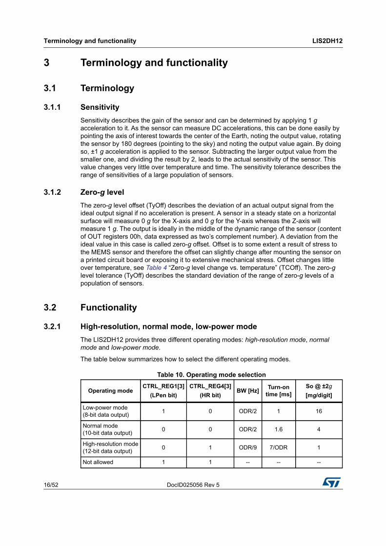
3.2.1 High-resolution, normal mode, low-power modeThe LIS2DH12 provides three different operating modes: high-resolution mode, normal mode and low-power mode.
The table below summarizes how to select the different operating modes.
Table 10. Operating mode selection
Operating modeCTRL_REG1[3]
(LPen bit)CTRL_REG4[3]
(HR bit)BW [Hz] Turn-on
time [ms]So @ ±2g[mg/digit]
Low-power mode (8-bit data output) 1 0 ODR/2 1 16
Normal mode(10-bit data output) 0 0 ODR/2 1.6 4
High-resolution mode(12-bit data output) 0 1 ODR/9 7/ODR 1
Not allowed 1 1 -- -- --
DocID025056 Rev 5 17/52
LIS2DH12 Terminology and functionality
52
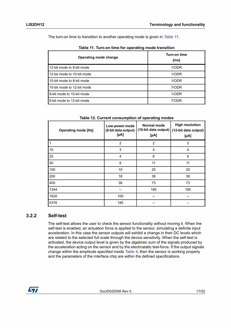
The turn-on time to transition to another operating mode is given in Table 11.
3.2.2 Self-testThe self-test allows the user to check the sensor functionality without moving it. When the self-test is enabled, an actuation force is applied to the sensor, simulating a definite input acceleration. In this case the sensor outputs will exhibit a change in their DC levels which are related to the selected full scale through the device sensitivity. When the self-test is activated, the device output level is given by the algebraic sum of the signals produced by the acceleration acting on the sensor and by the electrostatic test-force. If the output signals change within the amplitude specified inside Table 4, then the sensor is working properly and the parameters of the interface chip are within the defined specifications.
Table 11. Turn-on time for operating mode transition
Operating mode changeTurn-on time
[ms]
12-bit mode to 8-bit mode 1/ODR
12-bit mode to 10-bit mode 1/ODR
10-bit mode to 8-bit mode 1/ODR
10-bit mode to 12-bit mode 7/ODR
8-bit mode to 10-bit mode 1/ODR
8-bit mode to 12-bit mode 7/ODR
Table 12. Current consumption of operating modes
Operating mode [Hz]Low-power mode (8-bit data output)
[μA]
Normal mode (10-bit data output)
[μA]
High resolution(12-bit data output)
[μA]
1 2 2 2
10 3 4 4
25 4 6 6
50 6 11 11
100 10 20 20
200 18 38 38
400 36 73 73
1344 -- 185 185
1620 100 -- --
5376 185 -- --
Terminology and functionality LIS2DH12
18/52 DocID025056 Rev 5
3.2.3 6D / 4D orientation detectionThe LIS2DH12 provides the capability to detect the orientation of the device in space, enabling easy implementation of energy-saving procedures and automatic image rotation for mobile devices.
The 4D detection is a subset of the 6D function especially defined to be implemented in mobile devices for portrait and landscape computation. In 4D configuration, the Z-axis position detection is disabled.
3.2.4 “Sleep-to-wake” and “Return-to-sleep”The LIS2DH12 can be programmed to automatically switch to low-power mode upon recognition of a determined event.Once the event condition is over, the device returns back to the preset normal or high-resolution mode.
To enable this function the desired threshold value must be stored inside the ACT_THS (3Eh) register while the duration value is written inside the ACT_DUR (3Fh) register.
When the acceleration falls below the threshold value, the device automatically switches to low-power mode (10Hz ODR).During this condition, the ODR[3:0] bits and the LPen bit inside CTRL_REG1 (20h) and the HR bit in CTRL_REG4 (23h) are not considered.
As soon as the acceleration rises above threshold, the module restores the operating mode and ODRs as determined by the CTRL_REG1 (20h) and CTRL_REG4 (23h) settings.
3.3 Sensing element A proprietary process is used to create a surface micromachined accelerometer. The technology processes suspended silicon structures which are attached to the substrate in a few points called anchors and are free to move in the direction of the sensed acceleration. To be compatible with traditional packaging techniques, a cap is placed on top of the sensing element to avoid blocking the moving parts during the molding phase of the plastic encapsulation.
When an acceleration is applied to the sensor, the proof mass displaces from its nominal position, causing an imbalance in the capacitive half-bridge. This imbalance is measured using charge integration in response to a voltage pulse applied to the capacitor.
At steady state the nominal value of the capacitors are a few pF and when an acceleration is applied, the maximum variation of the capacitive load is in the fF range.
3.4 IC interfaceThe complete measurement chain is composed of a low-noise capacitive amplifier which converts the capacitive unbalance of the MEMS sensor into an analog voltage that will be available to the user through an analog-to-digital converter.
The acceleration data may be accessed through an I2C/SPI interface, thus making the device particularly suitable for direct interfacing with a microcontroller.
DocID025056 Rev 5 19/52
LIS2DH12 Terminology and functionality
52
The LIS2DH12 features a data-ready signal (DRDY) which indicates when a new set of measured acceleration data is available, thus simplifying data synchronization in the digital system that uses the device.
The LIS2DH12 may also be configured to generate an inertial wake-up and free-fall interrupt signal according to a programmed acceleration event along the enabled axes. Both free-fall and wake-up can be available simultaneously on two different pins.
3.5 Factory calibrationThe IC interface is factory calibrated for sensitivity (So) and zero-g level (TyOff).
The trim values are stored inside the device in non-volatile memory. Any time the device is turned on, these values are downloaded into the registers to be used during active operation. This allows using the device without further calibration.
3.6 FIFOThe LIS2DH12 contains a 10-bit, 32-level FIFO. Buffered output allows the following operation modes: FIFO, Stream, Stream-to-FIFO and FIFO bypass. When FIFO bypass mode is activated, FIFO is not operating and remains empty. In FIFO mode, measurement data from acceleration detection on the x, y, and z-axes are stored in the FIFO buffer.
3.7 Temperature sensorIn order to enable the internal temperature sensor, bits TEMP_EN[1:0] in register TEMP_CFG_REG (1Fh) and the BDU bit in CTRL_REG4 (23h) have to be set.
The temperature is available in OUT_TEMP_L (0Ch), OUT_TEMP_H (0Dh) stored as two’s complement data, left-justified.
The temperature data format can be 10 bits if LPen (bit 3) in CTRL_REG1 (20h) is cleared (high-resolution / normal mode), otherwise, in low-power mode, the ADC resolution is 8-bit.
Refer to Table 5: Temperature sensor characteristics for the conversion factor.
Application hints LIS2DH12
20/52 DocID025056 Rev 5
4 Application hints
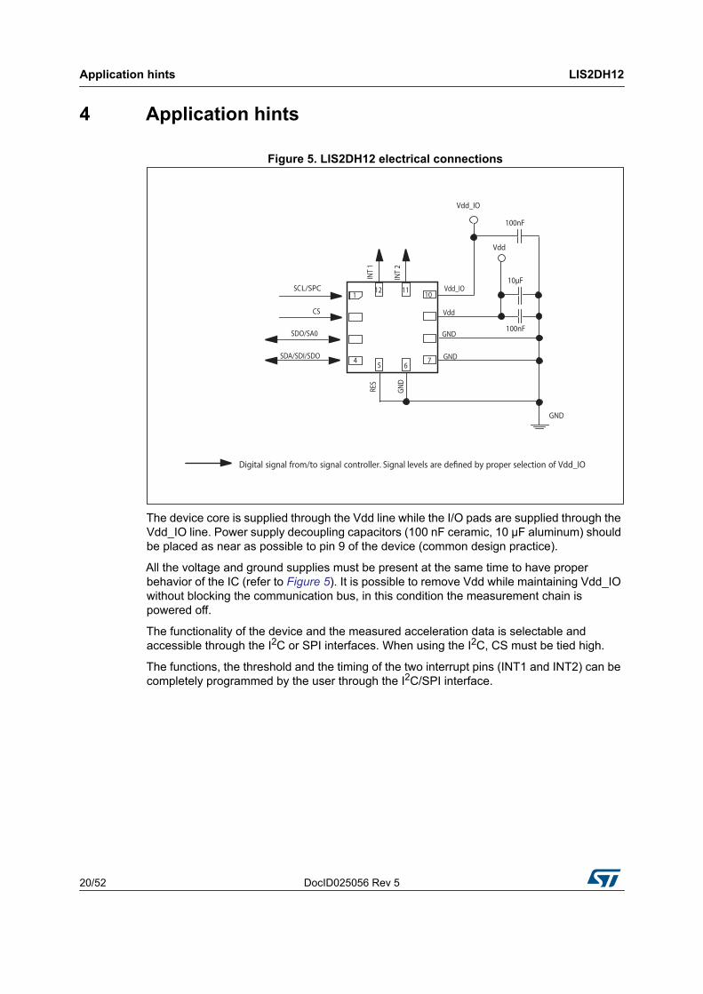
Figure 5. LIS2DH12 electrical connections
The device core is supplied through the Vdd line while the I/O pads are supplied through the Vdd_IO line. Power supply decoupling capacitors (100 nF ceramic, 10 μF aluminum) should be placed as near as possible to pin 9 of the device (common design practice).
All the voltage and ground supplies must be present at the same time to have proper behavior of the IC (refer to Figure 5). It is possible to remove Vdd while maintaining Vdd_IO without blocking the communication bus, in this condition the measurement chain is powered off.
The functionality of the device and the measured acceleration data is selectable and accessible through the I2C or SPI interfaces. When using the I2C, CS must be tied high.
The functions, the threshold and the timing of the two interrupt pins (INT1 and INT2) can be completely programmed by the user through the I2C/SPI interface.
Vdd_IO
Digital signal from/to signal controller. Signal levels are defined by proper selection of Vdd_IO
10μF
Vdd
100nF
GND
RES
SCL/SPC
SDA/SDI/SDO
CS
SDO/SA0 GND
GND
INT2
Vdd_IO
4
1
65GND
12
INT1
7
10
Vdd
100nF
11
DocID025056 Rev 5 21/52
LIS2DH12 Application hints
52
4.1 Soldering informationThe LGA package is compliant with the ECOPACK®, RoHS and “Green” standard.It is qualified for soldering heat resistance according to JEDEC J-STD-020.
Leave “Pin 1 Indicator” unconnected during soldering.
Land pattern and soldering recommendations are available at www.st.com.
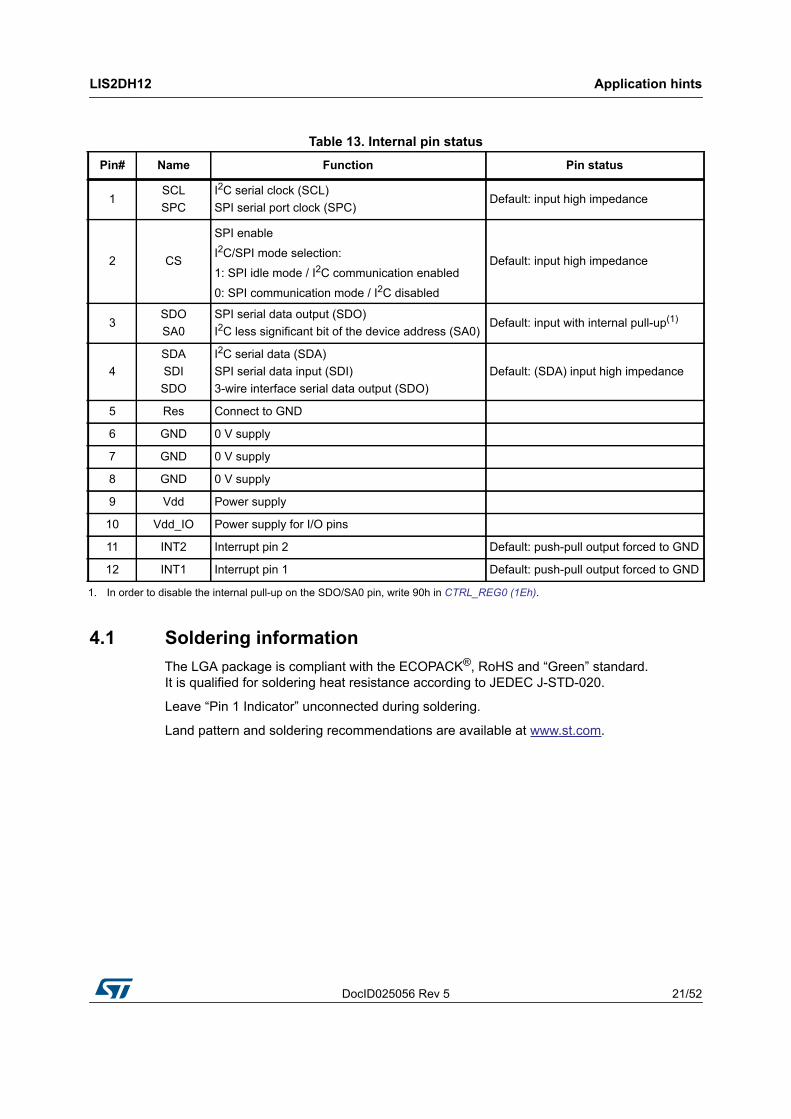
Table 13. Internal pin statusPin# Name Function Pin status
1SCLSPC
I2C serial clock (SCL)SPI serial port clock (SPC)
Default: input high impedance
2 CS
SPI enable
I2C/SPI mode selection:
1: SPI idle mode / I2C communication enabled
0: SPI communication mode / I2C disabled
Default: input high impedance
3SDOSA0
SPI serial data output (SDO)I2C less significant bit of the device address (SA0)
Default: input with internal pull-up(1)
4SDASDISDO
I2C serial data (SDA)SPI serial data input (SDI)3-wire interface serial data output (SDO)
Default: (SDA) input high impedance
5 Res Connect to GND
6 GND 0 V supply
7 GND 0 V supply
8 GND 0 V supply
9 Vdd Power supply
10 Vdd_IO Power supply for I/O pins
11 INT2 Interrupt pin 2 Default: push-pull output forced to GND
12 INT1 Interrupt pin 1 Default: push-pull output forced to GND
1. In order to disable the internal pull-up on the SDO/SA0 pin, write 90h in CTRL_REG0 (1Eh).
Digital main blocks LIS2DH12
22/52 DocID025056 Rev 5
5 Digital main blocks
5.1 FIFOThe LIS2DH12 embeds a 32-level FIFO for each of the three output channels, X, Y and Z. This allows consistent power saving for the system, since the host processor does not need to continuously poll data from the sensor, but it can wake up only when needed and burst the significant data out from the FIFO.
In order to enable the FIFO buffer, the FIFO_EN bit in CTRL_REG5 (24h) must be set to ‘1’.
This buffer can work according to the following different modes: Bypass mode, FIFO mode, Stream mode and Stream-to-FIFO mode. Each mode is selected by the FM [1:0] bits in FIFO_CTRL_REG (2Eh). Programmable FIFO watermark level, FIFO empty or FIFO overrun events can be enabled to generate dedicated interrupts on the INT1 pin (configuration through CTRL_REG3 (22h)).
In the FIFO_SRC_REG (2Fh) register the EMPTY bit is equal to ‘1’ when all FIFO samples are ready and FIFO is empty.
In the FIFO_SRC_REG (2Fh) register the WTM bit goes to ‘1’ if new data is written in the buffer and FIFO_SRC_REG (2Fh) (FSS [4:0]) is greater than or equal to FIFO_CTRL_REG (2Eh) (FTH [4:0]). FIFO_SRC_REG (2Fh) (WTM) goes to ‘0’ if reading an X, Y, Z data slot from FIFO and FIFO_SRC_REG (2Fh) (FSS [4:0]) is less than or equal to FIFO_CTRL_REG (2Eh) (FTH [4:0]).
In the FIFO_SRC_REG (2Fh) register the OVRN_FIFO bit is equal to ‘1’ if the FIFO slot is overwritten.
5.1.1 Bypass modeIn Bypass mode the FIFO is not operational and for this reason it remains empty. For each channel only the first address is used. The remaining FIFO levels are empty.
Bypass mode must be used in order to reset the FIFO buffer when a different mode is operating (i.e. FIFO mode).
5.1.2 FIFO modeIn FIFO mode, the buffer continues filling data from the X, Y and Z accelerometer channels until it is full (a set of 32 samples stored). When the FIFO is full, it stops collecting data from the input channels and the FIFO content remains unchanged.
An overrun interrupt can be enabled, I1_OVERRUN = '1' in the CTRL_REG3 (22h) register, in order to be raised when the FIFO stops collecting data. When the overrun interrupt occurs, the first data has been overwritten and the FIFO stops collecting data from the input channels.
After the last read it is necessary to transit from Bypass mode in order to reset the FIFO content. After this reset command, it is possible to restart FIFO mode just by selecting the FIFO mode configuration (FM[1:0] bits) in register FIFO_CTRL_REG (2Eh).
DocID025056 Rev 5 23/52
LIS2DH12 Digital main blocks
52
5.1.3 Stream modeIn Stream mode the FIFO continues filling data from the X, Y, and Z accelerometer channels until the buffer is full (a set of 32 samples stored) at which point the FIFO buffer index restarts from the beginning and older data is replaced by the current data. The oldest values continue to be overwritten until a read operation frees the FIFO slots.
An overrun interrupt can be enabled, I1_OVERRUN = '1' in the CTRL_REG3 (22h) register, in order to read the entire contents of the FIFO at once. If, in the application, it is mandatory not to lose data and it is not possible to read at least one sample for each axis within one ODR period, a watermark interrupt can be enabled in order to read partially the FIFO and leave memory slots free for incoming data.
Setting the FTH [4:0] bit in the FIFO_CTRL_REG (2Eh) register to an N value, the number of X, Y and Z data samples that should be read at the rise of the watermark interrupt is up to (N+1).
5.1.4 Stream-to-FIFO modeIn Stream-to-FIFO mode, data from the X, Y and Z accelerometer channels are collected in a combination of Stream mode and FIFO mode. The FIFO buffer starts operating in Stream mode and switches to FIFO mode when the selected interrupt occurs.
The FIFO operating mode changes according to the INT1 pin value if the TR bit is set to ‘0’ in the FIFO_CTRL_REG (2Eh) register or the INT2 pin value if the TR bit is set to‘1’ in the FIFO_CTRL_REG (2Eh) register.
When the interrupt pin is selected and the interrupt event is configured on the corresponding pin, the FIFO operates in Stream mode if the pin value is equal to ‘0’ and it operates in FIFO mode if the pin value is equal to ‘1’. Switching modes is dynamically performed according to the pin value.
Stream-to-FIFO can be used in order to analyze the sampling history that generates an interrupt. The standard operation is to read the contents of FIFO when the FIFO mode is triggered and the FIFO buffer is full and stopped.
5.1.5 Retrieving data from FIFOFIFO data is read from OUT_X_L (28h), OUT_X_H (29h), OUT_Y_L (2Ah), OUT_Y_H (2Bh) and OUT_Z_L (2Ch), OUT_Z_H (2Dh). When the FIFO is in Stream, Stream-to-FIFO or FIFO mode, a read operation to the OUT_X_L (28h), OUT_X_H (29h), OUT_Y_L (2Ah), OUT_Y_H (2Bh) or OUT_Z_L (2Ch), OUT_Z_H (2Dh) registers provides the data stored in the FIFO. Each time data is read from the FIFO, the oldest X, Y and Z data are placed in the OUT_X_L (28h), OUT_X_H (29h), OUT_Y_L (2Ah), OUT_Y_H (2Bh) and OUT_Z_L (2Ch), OUT_Z_H (2Dh) registers and both single read and read_burst operations can be used.
The address to be read is automatically updated by the device and it rolls back to 0x28 when register 0x2D is reached. In order to read all FIFO levels in a multiple byte read,192 bytes (6 output registers of 32 levels) have to be read.
Digital interfaces LIS2DH12
24/52 DocID025056 Rev 5
6 Digital interfaces
The registers embedded inside the LIS2DH12 may be accessed through both the I2C and SPI serial interfaces. The latter may be SW configured to operate either in 3-wire or 4-wire interface mode.
The serial interfaces are mapped to the same pads. To select/exploit the I2C interface, the CS line must be tied high (i.e. connected to Vdd_IO).
6.1 I2C serial interfaceThe LIS2DH12 I2C is a bus slave. The I2C is employed to write data into registers whose content can also be read back.
The relevant I2C terminology is given in the table below.
There are two signals associated with the I2C bus: the serial clock line (SCL) and the serial data line (SDA). The latter is a bidirectional line used for sending and receiving data to/from the interface. Both the lines must be connected to Vdd_IO through an external pull-up resistor. When the bus is free, both the lines are high.
The I2C interface is compliant with fast mode (400 kHz) I2C standards as well as with normal mode.
Table 14. Serial interface pin descriptionPin name Pin description
CS
SPI enableI2C/SPI mode selection:1: SPI idle mode / I2C communication enabled0: SPI communication mode / I2C disabled
SCLSPC
I2C serial clock (SCL)SPI serial port clock (SPC)
SDASDISDO
I2C serial data (SDA)SPI serial data input (SDI)3-wire interface serial data output (SDO)
SA0SDO
I2C less significant bit of the device address (SA0)SPI serial data output (SDO)
Table 15. I2C terminologyTerm Description
Transmitter The device which sends data to the bus
Receiver The device which receives data from the bus
Master The device which initiates a transfer, generates clock signals and terminates a transfer
Slave The device addressed by the master
DocID025056 Rev 5 25/52
LIS2DH12 Digital interfaces
52
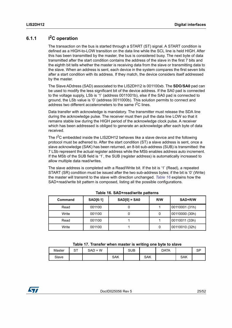
6.1.1 I2C operationThe transaction on the bus is started through a START (ST) signal. A START condition is defined as a HIGH-to-LOW transition on the data line while the SCL line is held HIGH. After this has been transmitted by the master, the bus is considered busy. The next byte of data transmitted after the start condition contains the address of the slave in the first 7 bits and the eighth bit tells whether the master is receiving data from the slave or transmitting data to the slave. When an address is sent, each device in the system compares the first seven bits after a start condition with its address. If they match, the device considers itself addressed by the master.
The Slave ADdress (SAD) associated to the LIS2DH12 is 001100xb. The SDO/SA0 pad can be used to modify the less significant bit of the device address. If the SA0 pad is connected to the voltage supply, LSb is ‘1’ (address 0011001b), else if the SA0 pad is connected to ground, the LSb value is ‘0’ (address 0011000b). This solution permits to connect and address two different accelerometers to the same I2C lines.
Data transfer with acknowledge is mandatory. The transmitter must release the SDA line during the acknowledge pulse. The receiver must then pull the data line LOW so that it remains stable low during the HIGH period of the acknowledge clock pulse. A receiver which has been addressed is obliged to generate an acknowledge after each byte of data received.
The I2C embedded inside the LIS2DH12 behaves like a slave device and the following protocol must be adhered to. After the start condition (ST) a slave address is sent, once a slave acknowledge (SAK) has been returned, an 8-bit sub-address (SUB) is transmitted: the 7 LSb represent the actual register address while the MSb enables address auto increment. If the MSb of the SUB field is ‘1’, the SUB (register address) is automatically increased to allow multiple data read/writes.
The slave address is completed with a Read/Write bit. If the bit is ‘1’ (Read), a repeated START (SR) condition must be issued after the two sub-address bytes; if the bit is ‘0’ (Write) the master will transmit to the slave with direction unchanged. Table 16 explains how the SAD+read/write bit pattern is composed, listing all the possible configurations.
Table 16. SAD+read/write patternsCommand SAD[6:1] SAD[0] = SA0 R/W SAD+R/W
Read 001100 0 1 00110001 (31h)
Write 001100 0 0 00110000 (30h)
Read 001100 1 1 00110011 (33h)
Write 001100 1 0 00110010 (32h)
Table 17. Transfer when master is writing one byte to slaveMaster ST SAD + W SUB DATA SP
Slave SAK SAK SAK
Digital interfaces LIS2DH12
26/52 DocID025056 Rev 5
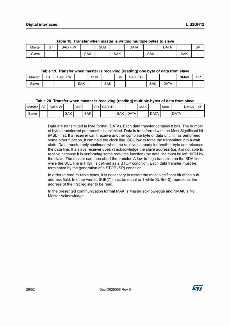
Data are transmitted in byte format (DATA). Each data transfer contains 8 bits. The number of bytes transferred per transfer is unlimited. Data is transferred with the Most Significant bit (MSb) first. If a receiver can’t receive another complete byte of data until it has performed some other function, it can hold the clock line, SCL low to force the transmitter into a wait state. Data transfer only continues when the receiver is ready for another byte and releases the data line. If a slave receiver doesn’t acknowledge the slave address (i.e. it is not able to receive because it is performing some real-time function) the data line must be left HIGH by the slave. The master can then abort the transfer. A low-to-high transition on the SDA line while the SCL line is HIGH is defined as a STOP condition. Each data transfer must be terminated by the generation of a STOP (SP) condition.
In order to read multiple bytes, it is necessary to assert the most significant bit of the sub-address field. In other words, SUB(7) must be equal to 1 while SUB(6-0) represents the address of the first register to be read.
In the presented communication format MAK is Master acknowledge and NMAK is No Master Acknowledge.
Table 18. Transfer when master is writing multiple bytes to slaveMaster ST SAD + W SUB DATA DATA SP
Slave SAK SAK SAK SAK
Table 19. Transfer when master is receiving (reading) one byte of data from slaveMaster ST SAD + W SUB SR SAD + R NMAK SP
Slave SAK SAK SAK DATA
Table 20. Transfer when master is receiving (reading) multiple bytes of data from slaveMaster ST SAD+W SUB SR SAD+R MAK MAK NMAK SP
Slave SAK SAK SAK DATA DATA DATA
DocID025056 Rev 5 27/52
LIS2DH12 Digital interfaces
52
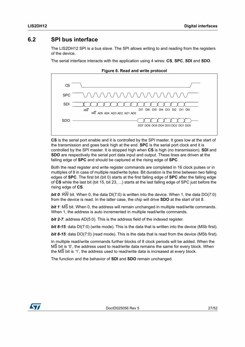
6.2 SPI bus interfaceThe LIS2DH12 SPI is a bus slave. The SPI allows writing to and reading from the registers of the device.
The serial interface interacts with the application using 4 wires: CS, SPC, SDI and SDO.
Figure 6. Read and write protocol
CS is the serial port enable and it is controlled by the SPI master. It goes low at the start of the transmission and goes back high at the end. SPC is the serial port clock and it is controlled by the SPI master. It is stopped high when CS is high (no transmission). SDI and SDO are respectively the serial port data input and output. These lines are driven at the falling edge of SPC and should be captured at the rising edge of SPC.
Both the read register and write register commands are completed in 16 clock pulses or in multiples of 8 in case of multiple read/write bytes. Bit duration is the time between two falling edges of SPC. The first bit (bit 0) starts at the first falling edge of SPC after the falling edge of CS while the last bit (bit 15, bit 23, ...) starts at the last falling edge of SPC just before the rising edge of CS.
bit 0: RW bit. When 0, the data DI(7:0) is written into the device. When 1, the data DO(7:0) from the device is read. In the latter case, the chip will drive SDO at the start of bit 8.
bit 1: MS bit. When 0, the address will remain unchanged in multiple read/write commands. When 1, the address is auto incremented in multiple read/write commands.
bit 2-7: address AD(5:0). This is the address field of the indexed register.
bit 8-15: data DI(7:0) (write mode). This is the data that is written into the device (MSb first).
bit 8-15: data DO(7:0) (read mode). This is the data that is read from the device (MSb first).
In multiple read/write commands further blocks of 8 clock periods will be added. When the MS bit is ‘0’, the address used to read/write data remains the same for every block. When the MS bit is ‘1’, the address used to read/write data is increased at every block.
The function and the behavior of SDI and SDO remain unchanged.
Digital interfaces LIS2DH12
28/52 DocID025056 Rev 5
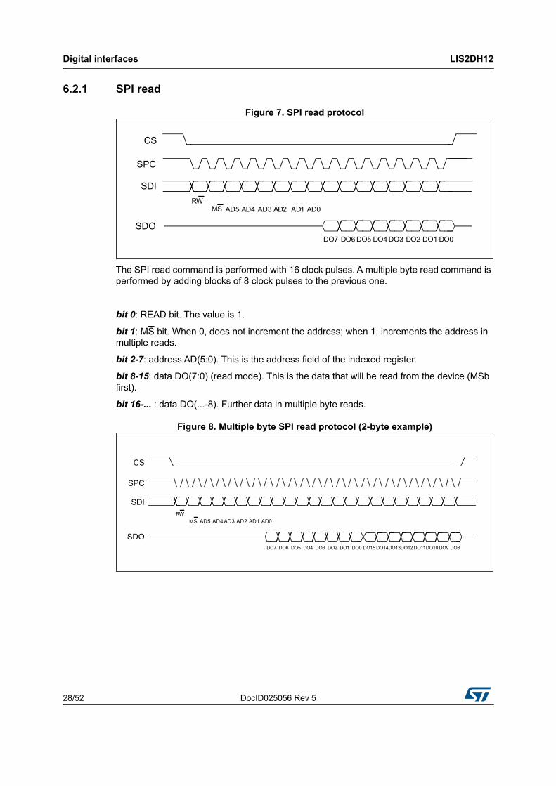
6.2.1 SPI read
Figure 7. SPI read protocol
The SPI read command is performed with 16 clock pulses. A multiple byte read command is performed by adding blocks of 8 clock pulses to the previous one.
bit 0: READ bit. The value is 1.
bit 1: MS bit. When 0, does not increment the address; when 1, increments the address in multiple reads.
bit 2-7: address AD(5:0). This is the address field of the indexed register.
bit 8-15: data DO(7:0) (read mode). This is the data that will be read from the device (MSb first).
bit 16-... : data DO(...-8). Further data in multiple byte reads.
Figure 8. Multiple byte SPI read protocol (2-byte example)
DocID025056 Rev 5 29/52
LIS2DH12 Digital interfaces
52
6.2.2 SPI write
Figure 9. SPI write protocol
The SPI write command is performed with 16 clock pulses. A multiple byte write command is performed by adding blocks of 8 clock pulses to the previous one.
bit 0: WRITE bit. The value is 0.
bit 1: MS bit. When 0, does not increment the address; when 1, increments the address in multiple writes.
bit 2 -7: address AD(5:0). This is the address field of the indexed register.
bit 8-15: data DI(7:0) (write mode). This is the data that is written inside the device (MSb first).
bit 16-... : data DI(...-8). Further data in multiple byte writes.
Figure 10. Multiple byte SPI write protocol (2-byte example)
Digital interfaces LIS2DH12
30/52 DocID025056 Rev 5
6.2.3 SPI read in 3-wire mode3-wire mode is entered by setting the SIM bit (SPI serial interface mode selection) to ‘1’ in CTRL_REG4 (23h).
Figure 11. SPI read protocol in 3-wire mode
The SPI read command is performed with 16 clock pulses.
bit 0: READ bit. The value is 1.
bit 1: MS bit. When 0, does not increment the address; when 1, increments the address in multiple reads.
bit 2-7: address AD(5:0). This is the address field of the indexed register.
bit 8-15: data DO(7:0) (read mode). This is the data that is read from the device (MSb first).
The multiple read command is also available in 3-wire mode.
DocID025056 Rev 5 31/52
LIS2DH12 Register mapping
52
7 Register mapping
The table given below provides a list of the 8-bit registers embedded in the device and the corresponding addresses.
Table 21. Register address map
Name TypeRegister address
Default CommentHex Binary
Reserved - 00 - 06 Reserved
STATUS_REG_AUX r 07 000 0111 Output
Reserved - 08-0B Reserved
OUT_TEMP_L r 0C 000 1100 Output
OUT_TEMP_H r 0D 000 1101 Output
Reserved - 0E 000 1110 Reserved
WHO_AM_I r 0F 000 1111 00110011 Dummy register
Reserved - 10 - 1D Reserved
CTRL_REG0 rw 1E 001 1110 00010000
TEMP_CFG_REG rw 1F 001 1111 00000000
CTRL_REG1 rw 20 010 0000 00000111
CTRL_REG2 rw 21 010 0001 00000000
CTRL_REG3 rw 22 010 0010 00000000
CTRL_REG4 rw 23 010 0011 00000000
CTRL_REG5 rw 24 010 0100 00000000
CTRL_REG6 rw 25 010 0101 00000000
REFERENCE rw 26 010 0110 00000000
STATUS_REG r 27 010 0111 Output
OUT_X_L r 28 010 1000 Output
OUT_X_H r 29 010 1001 Output
OUT_Y_L r 2A 010 1010 Output
OUT_Y_H r 2B 010 1011 Output
OUT_Z_L r 2C 010 1100 Output
OUT_Z_H r 2D 010 1101 Output
FIFO_CTRL_REG rw 2E 010 1110 00000000
FIFO_SRC_REG r 2F 010 1111 Output
INT1_CFG rw 30 011 0000 00000000
INT1_SRC r 31 011 0001 Output
INT1_THS rw 32 011 0010 00000000
Register mapping LIS2DH12
32/52 DocID025056 Rev 5
Registers marked as Reserved or not listed in the table above must not be changed. Writing to those registers may cause permanent damage to the device.
The content of the registers that are loaded at boot should not be changed. They contain the factory calibration values. Their content is automatically restored when the device is powered up.The boot procedure is complete within 5 milliseconds after device power-up.
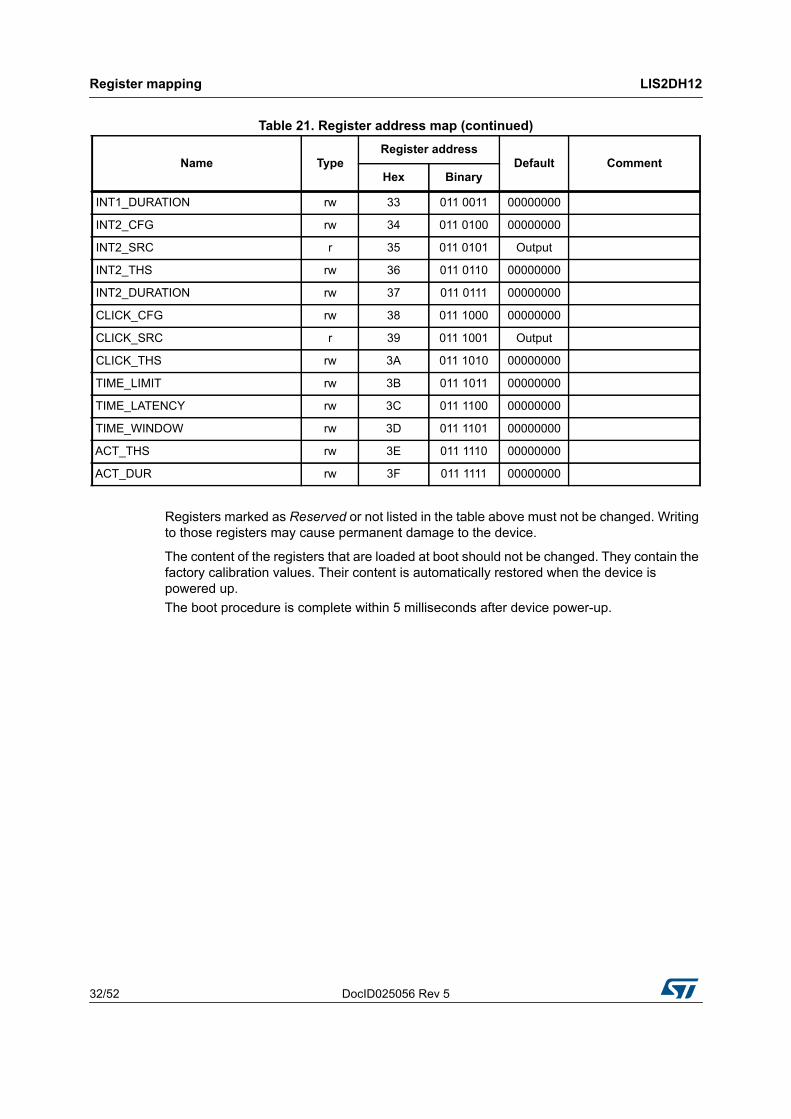
INT1_DURATION rw 33 011 0011 00000000
INT2_CFG rw 34 011 0100 00000000
INT2_SRC r 35 011 0101 Output
INT2_THS rw 36 011 0110 00000000
INT2_DURATION rw 37 011 0111 00000000
CLICK_CFG rw 38 011 1000 00000000
CLICK_SRC r 39 011 1001 Output
CLICK_THS rw 3A 011 1010 00000000
TIME_LIMIT rw 3B 011 1011 00000000
TIME_LATENCY rw 3C 011 1100 00000000
TIME_WINDOW rw 3D 011 1101 00000000
ACT_THS rw 3E 011 1110 00000000
ACT_DUR rw 3F 011 1111 00000000
Table 21. Register address map (continued)
Name TypeRegister address
Default CommentHex Binary
DocID025056 Rev 5 33/52
LIS2DH12 Register description
52
8 Register description
8.1 STATUS_REG_AUX (07h)
8.2 OUT_TEMP_L (0Ch), OUT_TEMP_H (0Dh)Temperature sensor data. Refer to Section 3.7: Temperature sensor for details on how to enable and read the temperature sensor output data.
8.3 WHO_AM_I (0Fh)
Device identification register.
8.4 CTRL_REG0 (1Eh)
Note: Leave bits 0 through 6 at the default value in order to ensure correct operation of the device.
Table 22. STATUS_REG_AUX register-- TOR -- -- -- TDA -- --
Table 23. STATUS_REG_AUX description TOR Temperature data overrun. Default value: 0
(0: no overrun has occurred; 1: new temperature data has overwritten the previous data)
TDA Temperature new data available. Default value: 0(0: new temperature data is not yet available;1: new temperature data is available)
Table 24. WHO_AM_I register0 0 1 1 0 0 1 1
Table 25. CTRL_REG0 registerSDO_PU_DISC 0(1)
1. This bit must be set to 0 for correct operation of the device.
0(1) 1(2)
2. This bit must be set to 1 for correct operation of the device.
0(1) 0(1) 0(1) 0(1)
Table 26. CTRL_REG0 description
SDO_PU_DISCDisconnect SDO/SA0 pull-up. Default value: 00010000(0: pull-up connected to SDO/SA0 pin; 1: pull-up disconnected to SDO/SA0 pin)
Register description LIS2DH12
34/52 DocID025056 Rev 5
8.5 TEMP_CFG_REG (1Fh)
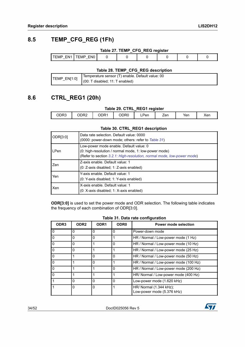
8.6 CTRL_REG1 (20h)
ODR[3:0] is used to set the power mode and ODR selection. The following table indicates the frequency of each combination of ODR[3:0].
Table 27. TEMP_CFG_REG registerTEMP_EN1 TEMP_EN0 0 0 0 0 0 0
Table 28. TEMP_CFG_REG description
TEMP_EN[1:0]Temperature sensor (T) enable. Default value: 00(00: T disabled; 11: T enabled)
Table 29. CTRL_REG1 registerODR3 ODR2 ODR1 ODR0 LPen Zen Yen Xen
Table 30. CTRL_REG1 description
ODR[3:0] Data rate selection. Default value: 0000(0000: power-down mode; others: refer to Table 31)
LPenLow-power mode enable. Default value: 0(0: high-resolution / normal mode, 1: low-power mode)(Refer to section 3.2.1: High-resolution, normal mode, low-power mode)
ZenZ-axis enable. Default value: 1(0: Z-axis disabled; 1: Z-axis enabled)
YenY-axis enable. Default value: 1(0: Y-axis disabled; 1: Y-axis enabled)
XenX-axis enable. Default value: 1(0: X-axis disabled; 1: X-axis enabled)
Table 31. Data rate configurationODR3 ODR2 ODR1 ODR0 Power mode selection
0 0 0 0 Power-down mode
0 0 0 1 HR / Normal / Low-power mode (1 Hz)
0 0 1 0 HR / Normal / Low-power mode (10 Hz)
0 0 1 1 HR / Normal / Low-power mode (25 Hz)
0 1 0 0 HR / Normal / Low-power mode (50 Hz)
0 1 0 1 HR / Normal / Low-power mode (100 Hz)
0 1 1 0 HR / Normal / Low-power mode (200 Hz)
0 1 1 1 HR/ Normal / Low-power mode (400 Hz)
1 0 0 0 Low-power mode (1.620 kHz)
1 0 0 1 HR/ Normal (1.344 kHz);Low-power mode (5.376 kHz)

DocID025056 Rev 5 35/52
LIS2DH12 Register description
52
8.7 CTRL_REG2 (21h)
8.8 CTRL_REG3 (22h)
Table 32. CTRL_REG2 registerHPM1 HPM0 HPCF2 HPCF1 FDS HPCLICK HP_IA2 HP_IA1
Table 33. CTRL_REG2 descriptionHPM[1:0] High-pass filter mode selection. Default value: 00
Refer to Table 34 for filter mode configurationHPCF[2:1] High-pass filter cutoff frequency selection
FDS Filtered data selection. Default value: 0(0: internal filter bypassed; 1: data from internal filter sent to output register and FIFO)
HPCLICKHigh-pass filter enabled for CLICK function.(0: filter bypassed; 1: filter enabled)
HP_IA2 High-pass filter enabled for AOI function on Interrupt 2. (0: filter bypassed; 1: filter enabled)
HP_IA1 High-pass filter enabled for AOI function on Interrupt 1.(0: filter bypassed; 1: filter enabled)
Table 34. High-pass filter mode configurationHPM1 HPM0 High-pass filter mode
0 0 Normal mode (reset by reading REFERENCE (26h) register)
0 1 Reference signal for filtering
1 0 Normal mode
1 1 Autoreset on interrupt event
Table 35. CTRL_REG3 registerI1_CLICK I1_IA1 I1_IA2 I1_ZYXDA 0(1)
1. This bit must be set to ‘0’ for correct operation of the device.
I1_WTM I1_OVERRUN --
Table 36. CTRL_REG3 description I1_CLICK CLICK interrupt on INT1 pin. Default value: 0
(0: disable; 1: enable)I1_IA1 IA1 interrupt on INT1 pin. Default value: 0
(0: disable; 1: enable)I1_IA2 IA2 interrupt on INT1 pin. Default value: 0
(0: disable; 1: enable)I1_ZYXDA ZYXDA interrupt on INT1 pin. Default value: 0
(0: disable; 1: enable)I1_WTM FIFO watermark interrupt on INT1 pin. Default value: 0
(0: disable; 1: enable)I1_OVERRUN FIFO overrun interrupt on INT1 pin. Default value: 0
(0: disable; 1: enable)
Register description LIS2DH12
36/52 DocID025056 Rev 5
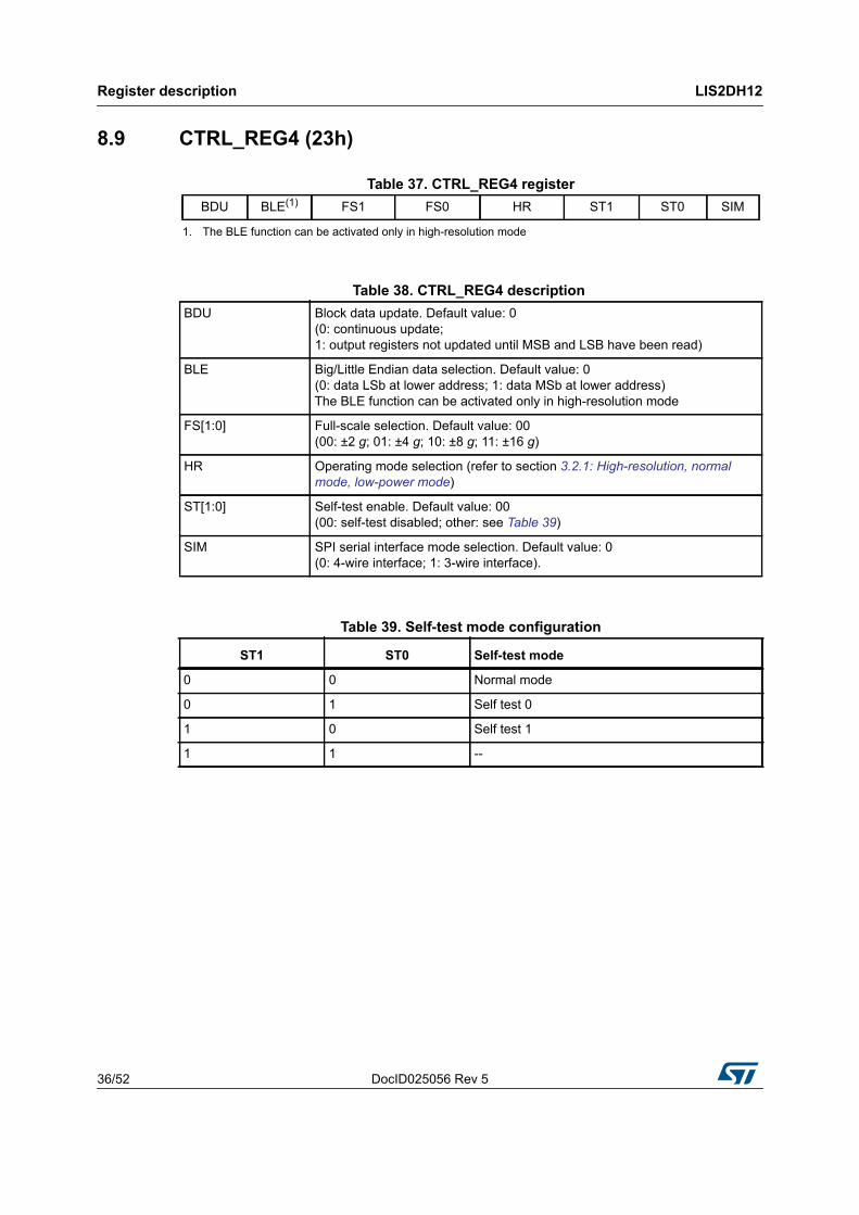
8.9 CTRL_REG4 (23h)
Table 37. CTRL_REG4 registerBDU BLE(1)
1. The BLE function can be activated only in high-resolution mode
FS1 FS0 HR ST1 ST0 SIM
Table 38. CTRL_REG4 description BDU Block data update. Default value: 0
(0: continuous update; 1: output registers not updated until MSB and LSB have been read)
BLE Big/Little Endian data selection. Default value: 0(0: data LSb at lower address; 1: data MSb at lower address)The BLE function can be activated only in high-resolution mode
FS[1:0] Full-scale selection. Default value: 00(00: ±2 g; 01: ±4 g; 10: ±8 g; 11: ±16 g)
HR Operating mode selection (refer to section 3.2.1: High-resolution, normal mode, low-power mode)
ST[1:0] Self-test enable. Default value: 00(00: self-test disabled; other: see Table 39)
SIM SPI serial interface mode selection. Default value: 0(0: 4-wire interface; 1: 3-wire interface).
Table 39. Self-test mode configuration
ST1 ST0 Self-test mode
0 0 Normal mode
0 1 Self test 0
1 0 Self test 1
1 1 --
DocID025056 Rev 5 37/52
LIS2DH12 Register description
52
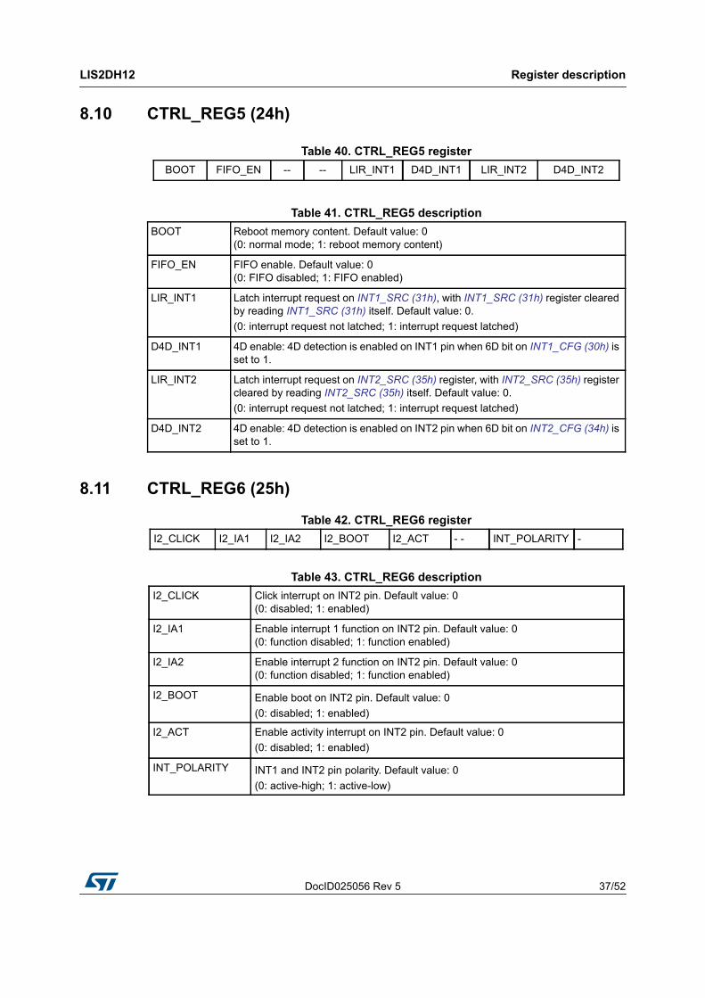
8.10 CTRL_REG5 (24h)
8.11 CTRL_REG6 (25h)
Table 40. CTRL_REG5 registerBOOT FIFO_EN -- -- LIR_INT1 D4D_INT1 LIR_INT2 D4D_INT2
Table 41. CTRL_REG5 descriptionBOOT Reboot memory content. Default value: 0
(0: normal mode; 1: reboot memory content)
FIFO_EN FIFO enable. Default value: 0 (0: FIFO disabled; 1: FIFO enabled)
LIR_INT1 Latch interrupt request on INT1_SRC (31h), with INT1_SRC (31h) register cleared by reading INT1_SRC (31h) itself. Default value: 0.(0: interrupt request not latched; 1: interrupt request latched)
D4D_INT1 4D enable: 4D detection is enabled on INT1 pin when 6D bit on INT1_CFG (30h) is set to 1.
LIR_INT2 Latch interrupt request on INT2_SRC (35h) register, with INT2_SRC (35h) register cleared by reading INT2_SRC (35h) itself. Default value: 0.(0: interrupt request not latched; 1: interrupt request latched)
D4D_INT2 4D enable: 4D detection is enabled on INT2 pin when 6D bit on INT2_CFG (34h) is set to 1.
Table 42. CTRL_REG6 registerI2_CLICK I2_IA1 I2_IA2 I2_BOOT I2_ACT - - INT_POLARITY -
Table 43. CTRL_REG6 descriptionI2_CLICK Click interrupt on INT2 pin. Default value: 0
(0: disabled; 1: enabled)
I2_IA1 Enable interrupt 1 function on INT2 pin. Default value: 0(0: function disabled; 1: function enabled)
I2_IA2 Enable interrupt 2 function on INT2 pin. Default value: 0(0: function disabled; 1: function enabled)
I2_BOOT Enable boot on INT2 pin. Default value: 0(0: disabled; 1: enabled)
I2_ACT Enable activity interrupt on INT2 pin. Default value: 0(0: disabled; 1: enabled)
INT_POLARITY INT1 and INT2 pin polarity. Default value: 0(0: active-high; 1: active-low)

Register description LIS2DH12
38/52 DocID025056 Rev 5
8.12 REFERENCE (26h)
8.13 STATUS_REG (27h)
Table 44. REFERENCE registerRef7 Ref6 Ref5 Ref4 Ref3 Ref2 Ref1 Ref0
Table 45. REFERENCE description Ref [7:0] Reference value for interrupt generation. Default value: 0
Table 46. STATUS_REG registerZYXOR ZOR YOR XOR ZYXDA ZDA YDA XDA
Table 47. STATUS_REG description ZYXOR X-, Y- and Z-axis data overrun. Default value: 0
(0: no overrun has occurred; 1: a new set of data has overwritten the previous set)
ZOR Z-axis data overrun. Default value: 0(0: no overrun has occurred; 1: new data for the Z-axis has overwritten the previous data)
YOR Y-axis data overrun. Default value: 0(0: no overrun has occurred; 1: new data for the Y-axis has overwritten the previous data)
XOR X-axis data overrun. Default value: 0(0: no overrun has occurred; 1: new data for the X-axis has overwritten the previous data)
ZYXDA X-, Y- and Z-axis new data available. Default value: 0(0: a new set of data is not yet available; 1: a new set of data is available)
ZDA Z-axis new data available. Default value: 0(0: new data for the Z-axis is not yet available; 1: new data for the Z-axis is available)
YDA Y-axis new data available. Default value: 0(0: new data for the Y-axis is not yet available; 1: new data for the Y-axis is available)

DocID025056 Rev 5 39/52
LIS2DH12 Register description
52
8.14 OUT_X_L (28h), OUT_X_H (29h)X-axis acceleration data. The value is expressed as two’s complement left-justified.Please refer to Section 3.2.1: High-resolution, normal mode, low-power mode.
8.15 OUT_Y_L (2Ah), OUT_Y_H (2Bh)Y-axis acceleration data. The value is expressed as two’s complement left-justified.Please refer to Section 3.2.1: High-resolution, normal mode, low-power mode.
8.16 OUT_Z_L (2Ch), OUT_Z_H (2Dh)Z-axis acceleration data. The value is expressed as two’s complement left-justified.Please refer to Section 3.2.1: High-resolution, normal mode, low-power mode.
8.17 FIFO_CTRL_REG (2Eh)
Table 48. FIFO_CTRL_REG registerFM1 FM0 TR FTH4 FTH3 FTH2 FTH1 FTH0
Table 49. FIFO_CTRL_REG description FM[1:0] FIFO mode selection. Default value: 00 (see Table 50)
TR Trigger selection. Default value: 00: trigger event allows triggering signal on INT1 1: trigger event allows triggering signal on INT2
FTH[4:0] Default value: 00000
Table 50. FIFO mode configuration
FM1 FM0 FIFO mode
0 0 Bypass mode
0 1 FIFO mode
1 0 Stream mode
1 1 Stream-to-FIFO mode
Register description LIS2DH12
40/52 DocID025056 Rev 5
8.18 FIFO_SRC_REG (2Fh)
Table 52. FIFO_SRC_REG description
8.19 INT1_CFG (30h)
The content of this register is loaded at boot.
Table 51. FIFO_SRC_REG registerWTM OVRN_FIFO EMPTY FSS4 FSS3 FSS2 FSS1 FSS0
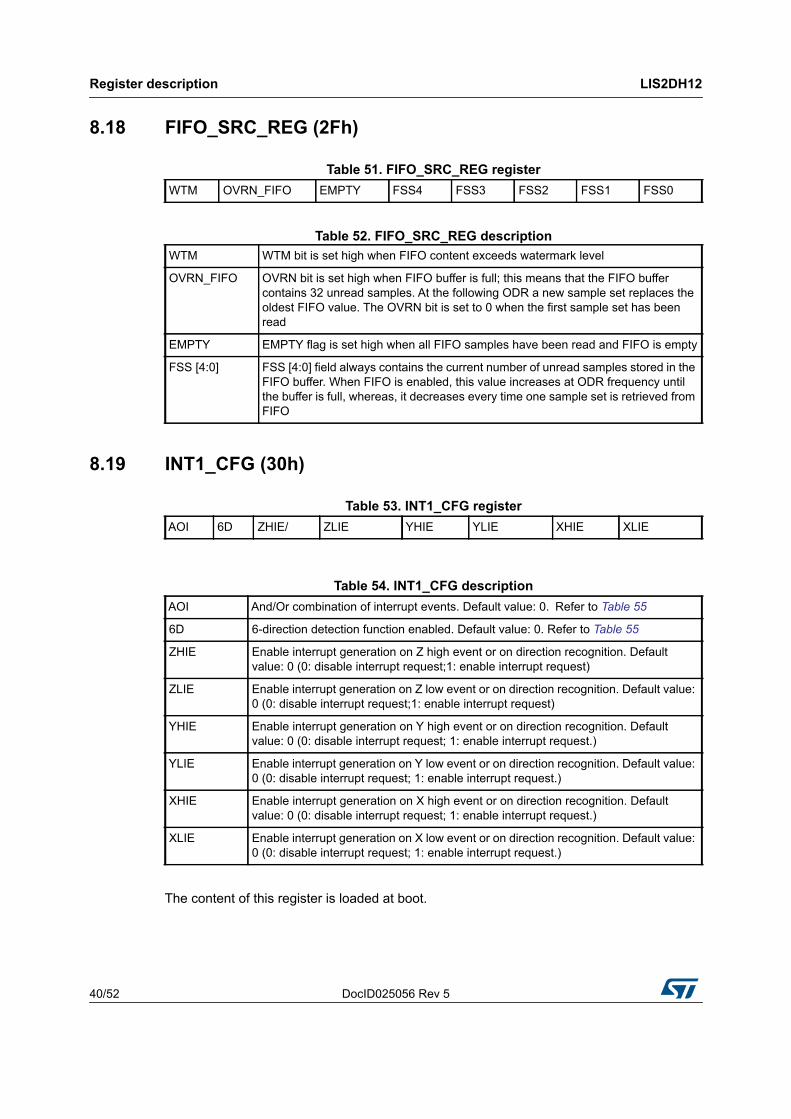
WTM WTM bit is set high when FIFO content exceeds watermark level
OVRN_FIFO OVRN bit is set high when FIFO buffer is full; this means that the FIFO buffer contains 32 unread samples. At the following ODR a new sample set replaces the oldest FIFO value. The OVRN bit is set to 0 when the first sample set has been read
EMPTY EMPTY flag is set high when all FIFO samples have been read and FIFO is empty
FSS [4:0] FSS [4:0] field always contains the current number of unread samples stored in the FIFO buffer. When FIFO is enabled, this value increases at ODR frequency until the buffer is full, whereas, it decreases every time one sample set is retrieved from FIFO
Table 53. INT1_CFG registerAOI 6D ZHIE/ ZLIE YHIE YLIE XHIE XLIE
Table 54. INT1_CFG descriptionAOI And/Or combination of interrupt events. Default value: 0. Refer to Table 55
6D 6-direction detection function enabled. Default value: 0. Refer to Table 55
ZHIE Enable interrupt generation on Z high event or on direction recognition. Default value: 0 (0: disable interrupt request;1: enable interrupt request)
ZLIE Enable interrupt generation on Z low event or on direction recognition. Default value: 0 (0: disable interrupt request;1: enable interrupt request)
YHIE Enable interrupt generation on Y high event or on direction recognition. Default value: 0 (0: disable interrupt request; 1: enable interrupt request.)
YLIE Enable interrupt generation on Y low event or on direction recognition. Default value: 0 (0: disable interrupt request; 1: enable interrupt request.)
XHIE Enable interrupt generation on X high event or on direction recognition. Default value: 0 (0: disable interrupt request; 1: enable interrupt request.)
XLIE Enable interrupt generation on X low event or on direction recognition. Default value: 0 (0: disable interrupt request; 1: enable interrupt request.)
DocID025056 Rev 5 41/52
LIS2DH12 Register description
52
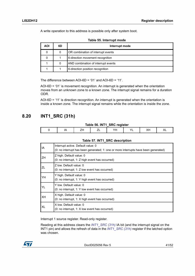
A write operation to this address is possible only after system boot.
The difference between AOI-6D = ‘01’ and AOI-6D = ‘11’.
AOI-6D = ‘01’ is movement recognition. An interrupt is generated when the orientation moves from an unknown zone to a known zone. The interrupt signal remains for a duration ODR.
AOI-6D = ‘11’ is direction recognition. An interrupt is generated when the orientation is inside a known zone. The interrupt signal remains while the orientation is inside the zone.
8.20 INT1_SRC (31h)
Interrupt 1 source register. Read-only register.
Reading at this address clears the INT1_SRC (31h) IA bit (and the interrupt signal on the INT1 pin) and allows the refresh of data in the INT1_SRC (31h) register if the latched option was chosen.
Table 55. Interrupt modeAOI 6D Interrupt mode
0 0 OR combination of interrupt events
0 1 6-direction movement recognition
1 0 AND combination of interrupt events
1 1 6-direction position recognition
Table 56. INT1_SRC register0 IA ZH ZL YH YL XH XL
Table 57. INT1_SRC description
IAInterrupt active. Default value: 0(0: no interrupt has been generated; 1: one or more interrupts have been generated)
ZHZ high. Default value: 0(0: no interrupt, 1: Z high event has occurred)
ZLZ low. Default value: 0(0: no interrupt; 1: Z low event has occurred)
YHY high. Default value: 0(0: no interrupt, 1: Y high event has occurred)
YLY low. Default value: 0(0: no interrupt, 1: Y low event has occurred)
XHX high. Default value: 0(0: no interrupt, 1: X high event has occurred)
XLX low. Default value: 0(0: no interrupt, 1: X low event has occurred)
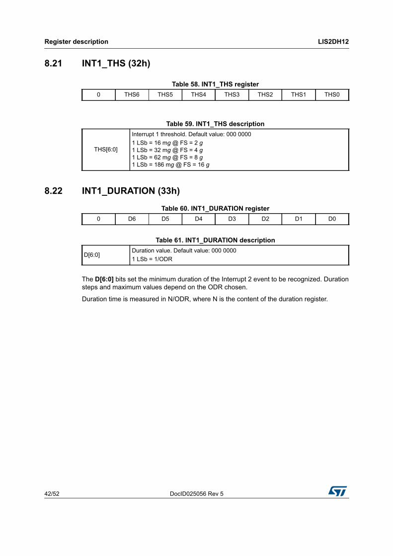
Register description LIS2DH12
42/52 DocID025056 Rev 5
8.21 INT1_THS (32h)
8.22 INT1_DURATION (33h)
The D[6:0] bits set the minimum duration of the Interrupt 2 event to be recognized. Durationsteps and maximum values depend on the ODR chosen.
Duration time is measured in N/ODR, where N is the content of the duration register.
Table 58. INT1_THS register0 THS6 THS5 THS4 THS3 THS2 THS1 THS0
Table 59. INT1_THS description
THS[6:0]
Interrupt 1 threshold. Default value: 000 00001 LSb = 16 mg @ FS = 2 g1 LSb = 32 mg @ FS = 4 g1 LSb = 62 mg @ FS = 8 g1 LSb = 186 mg @ FS = 16 g
Table 60. INT1_DURATION register0 D6 D5 D4 D3 D2 D1 D0
Table 61. INT1_DURATION description
D[6:0]Duration value. Default value: 000 00001 LSb = 1/ODR
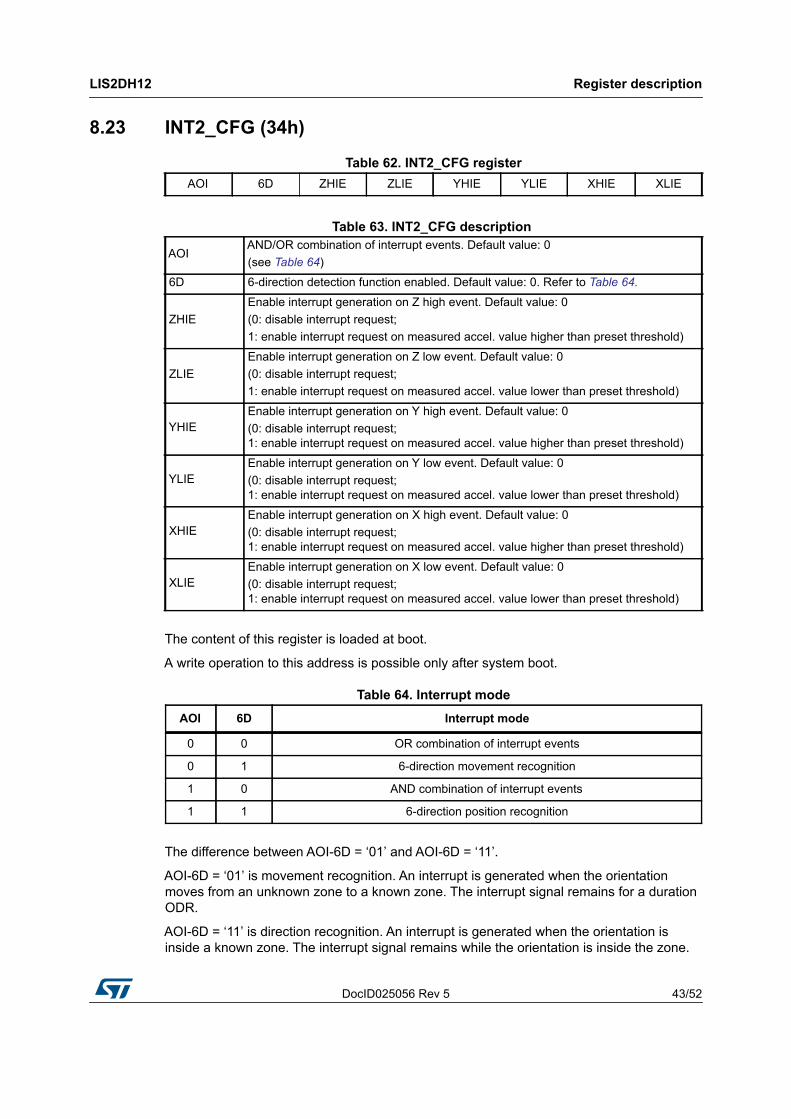
DocID025056 Rev 5 43/52
LIS2DH12 Register description
52
8.23 INT2_CFG (34h)
The content of this register is loaded at boot.
A write operation to this address is possible only after system boot.
The difference between AOI-6D = ‘01’ and AOI-6D = ‘11’.
AOI-6D = ‘01’ is movement recognition. An interrupt is generated when the orientation moves from an unknown zone to a known zone. The interrupt signal remains for a duration ODR.
AOI-6D = ‘11’ is direction recognition. An interrupt is generated when the orientation is inside a known zone. The interrupt signal remains while the orientation is inside the zone.
Table 62. INT2_CFG registerAOI 6D ZHIE ZLIE YHIE YLIE XHIE XLIE
Table 63. INT2_CFG description
AOIAND/OR combination of interrupt events. Default value: 0(see Table 64)
6D 6-direction detection function enabled. Default value: 0. Refer to Table 64.
ZHIEEnable interrupt generation on Z high event. Default value: 0(0: disable interrupt request;1: enable interrupt request on measured accel. value higher than preset threshold)
ZLIEEnable interrupt generation on Z low event. Default value: 0(0: disable interrupt request;1: enable interrupt request on measured accel. value lower than preset threshold)
YHIEEnable interrupt generation on Y high event. Default value: 0(0: disable interrupt request;1: enable interrupt request on measured accel. value higher than preset threshold)
YLIEEnable interrupt generation on Y low event. Default value: 0(0: disable interrupt request;1: enable interrupt request on measured accel. value lower than preset threshold)
XHIEEnable interrupt generation on X high event. Default value: 0 (0: disable interrupt request;1: enable interrupt request on measured accel. value higher than preset threshold)
XLIEEnable interrupt generation on X low event. Default value: 0 (0: disable interrupt request;1: enable interrupt request on measured accel. value lower than preset threshold)
Table 64. Interrupt modeAOI 6D Interrupt mode
0 0 OR combination of interrupt events
0 1 6-direction movement recognition
1 0 AND combination of interrupt events
1 1 6-direction position recognition
Register description LIS2DH12
44/52 DocID025056 Rev 5
8.24 INT2_SRC (35h)
Interrupt 2 source register. Read-only register.
Reading at this address clears the INT2_SRC (35h) IA bit (and the interrupt signal on the INT2 pin) and allows the refresh of data in the INT2_SRC (35h) register if the latched option was chosen.
8.25 INT2_THS (36h)
Table 65. INT2_SRC register0 IA ZH ZL YH YL XH XL
Table 66. INT2_SRC description
IAInterrupt active. Default value: 0(0: no interrupt has been generated; 1: one or more interrupts have been generated)
ZHZ high. Default value: 0(0: no interrupt, 1: Z high event has occurred)
ZLZ low. Default value: 0(0: no interrupt; 1: Z low event has occurred)
YHY high. Default value: 0(0: no interrupt, 1: Y high event has occurred)
YLY low. Default value: 0(0: no interrupt, 1: Y low event has occurred)
XHX high. Default value: 0(0: no interrupt, 1: X high event has occurred)
XLX low. Default value: 0(0: no interrupt, 1: X low event has occurred)
Table 67. INT2_THS register0 THS6 THS5 THS4 THS3 THS2 THS1 THS0
Table 68. INT2_THS description
THS[6:0]
Interrupt 2 threshold. Default value: 000 0000
1 LSb = 16 mg @ FS = 2 g 1 LSb = 32 mg @ FS = 4 g 1 LSb = 62 mg @ FS = 8 g 1 LSb = 186 mg @ FS = 16 g
DocID025056 Rev 5 45/52
LIS2DH12 Register description
52
8.26 INT2_DURATION (37h)
The D[6:0] bits set the minimum duration of the Interrupt 2 event to be recognized. Duration time steps and maximum values depend on the ODR chosen.
8.27 CLICK_CFG (38h)
Table 69. INT2_DURATION register0 D6 D5 D4 D3 D2 D1 D0
Table 70. INT2_DURATION description
D[6:0]Duration value. Default value: 000 00001 LSb = 1/ODR(1)
1. Duration time is measured in N/ODR, where N is the content of the duration register.
Table 71. CLICK_CFG register-- -- ZD ZS YD YS XD XS
Table 72. CLICK_CFG description ZD Enable interrupt double-click on Z-axis. Default value: 0
(0: disable interrupt request; 1: enable interrupt request on measured accel. value higher than preset threshold)
ZS Enable interrupt single-click on Z-axis. Default value: 0(0: disable interrupt request; 1: enable interrupt request on measured accel. value higher than preset threshold)
YD Enable interrupt double-click on Y-axis. Default value: 0(0: disable interrupt request; 1: enable interrupt request on measured accel. value higher than preset threshold)
YS Enable interrupt single-click on Y-axis. Default value: 0(0: disable interrupt request; 1: enable interrupt request on measured accel. value higher than preset threshold)
XD Enable interrupt double-click on X-axis. Default value: 0(0: disable interrupt request; 1: enable interrupt request on measured accel. value higher than preset threshold)
XS Enable interrupt single-click on X-axis. Default value: 0(0: disable interrupt request; 1: enable interrupt request on measured accel. value higher than preset threshold)
Register description LIS2DH12
46/52 DocID025056 Rev 5
8.28 CLICK_SRC (39h)
8.29 CLICK_THS (3Ah)
8.30 TIME_LIMIT (3Bh)
Table 73. CLICK_SRC registerIA DClick SClick Sign Z Y X
Table 74. CLICK_SRC description IA Interrupt active. Default value: 0
(0: no interrupt has been generated; 1: one or more interrupts have been generated)
DClick Double-click enable. Default value: 0 (0: double-click detection disabled, 1: double-click detection enabled)
SClick Single-click enable. Default value: 0 (0: single-click detection disabled, 1: single-click detection enabled)
Sign Click sign. 0: positive detection, 1: negative detection
Z Z click detection. Default value: 0(0: no interrupt, 1: Z high event has occurred)
Y Y click detection. Default value: 0(0: no interrupt, 1: Y high event has occurred)
X X click detection. Default value: 0(0: no interrupt, 1: X high event has occurred)
Table 75. CLICK_THS registerLIR_Click Ths6 Ths5 Ths4 Ths3 Ths2 Ths1 Ths0
Table 76. CLICK_THS register description
LIR_Click
If the LIR_Click bit is not set, the interrupt is kept high for the duration of the latency window.If the LIR_Click bit is set, the interrupt is kept high until the CLICK_SRC (39h) register is read.
Ths[6:0] Click threshold. Default value: 000 0000
Table 77. TIME_LIMIT register- TLI6 TLI5 TLI4 TLI3 TLI2 TLI1 TLI0
Table 78. TIME_LIMIT descriptionTLI[6:0] Click time limit. Default value: 000 0000

DocID025056 Rev 5 47/52
LIS2DH12 Register description
52
8.31 TIME_LATENCY (3Ch)
8.32 TIME_WINDOW (3Dh)
8.33 ACT_THS (3Eh)
8.34 ACT_DUR (3Fh)
Table 79. TIME_LATENCY registerTLA7 TLA6 TLA5 TLA4 TLA3 TLA2 TLA1 TLA0
Table 80. TIME_LATENCY descriptionTLA[7:0] Click time latency. Default value: 0000 0000
Table 81. TIME_WINDOW registerTW7 TW6 TW5 TW4 TW3 TW2 TW1 TW0
Table 82. TIME_WINDOW descriptionTW[7:0] Click time window
Table 83. ACT_THS register-- Acth6 Acth5 Acth4 Acth3 Acth2 Acth1 Acth0
Table 84. ACT_THS descriptionActh[6:0] Sleep-to-wake, return-to-sleep activation threshold in low-power mode
1 LSb = 16 mg @ FS = 2 g1 LSb = 32 mg @ FS = 4 g1 LSb = 62 mg @ FS = 8 g1 LSb = 186 mg @ FS = 16 g
Table 85. ACT_DUR registerActD7 ActD6 ActD5 ActD4 ActD3 ActD2 ActD1 ActD0
Table 86. ACT_DUR descriptionActD[7:0] Sleep-to-wake, return-to-sleep duration.
1 LSb = (8*1[LSb]+1)/ODR
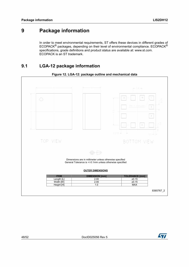
Package information LIS2DH12
48/52 DocID025056 Rev 5
9 Package information
In order to meet environmental requirements, ST offers these devices in different grades ofECOPACK® packages, depending on their level of environmental compliance. ECOPACK®
specifications, grade definitions and product status are available at: www.st.com. ECOPACK is an ST trademark.
9.1 LGA-12 package information
Figure 12. LGA-12: package outline and mechanical data
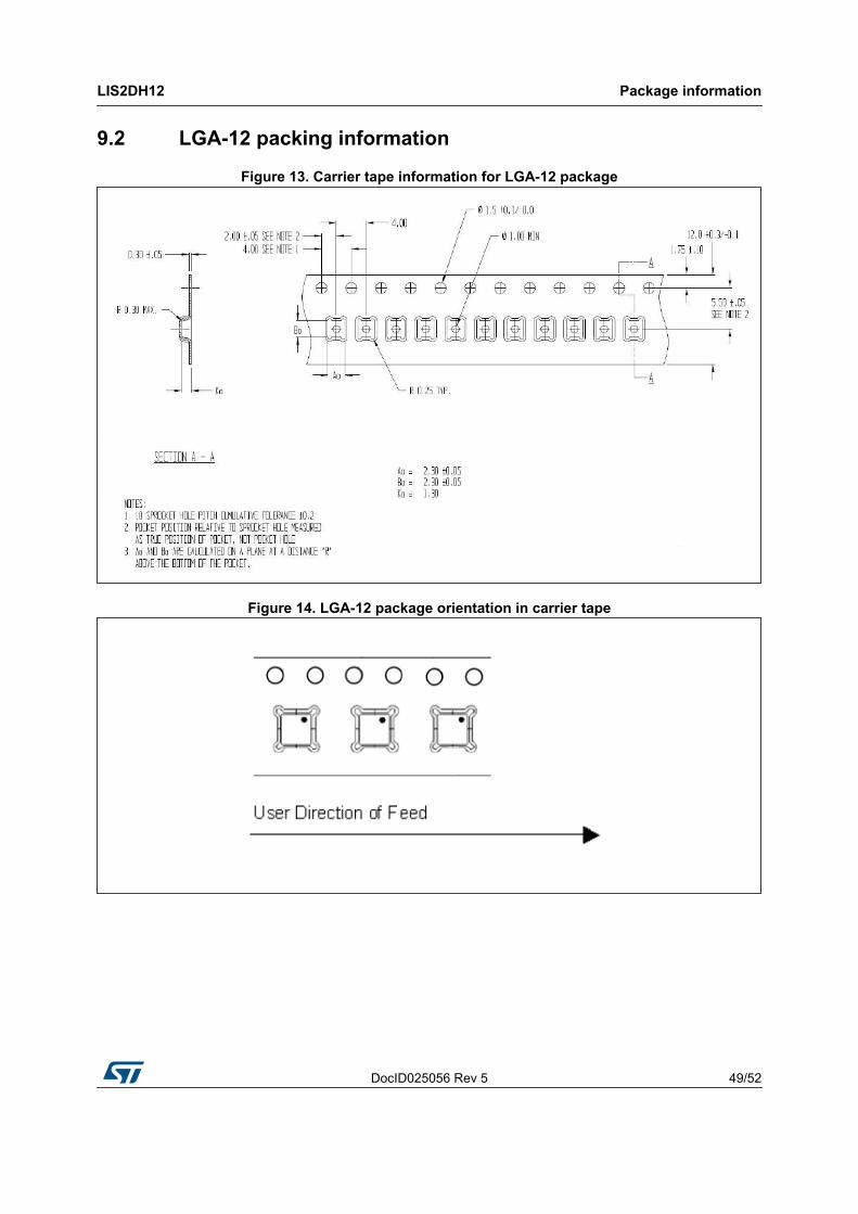
DocID025056 Rev 5 49/52
LIS2DH12 Package information
52
9.2 LGA-12 packing information
Figure 13. Carrier tape information for LGA-12 package
Figure 14. LGA-12 package orientation in carrier tape
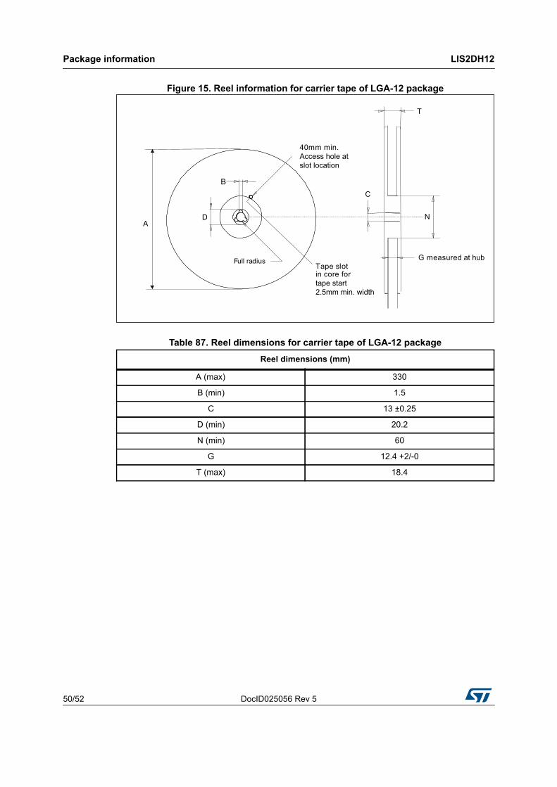
Package information LIS2DH12
50/52 DocID025056 Rev 5
Figure 15. Reel information for carrier tape of LGA-12 package
Table 87. Reel dimensions for carrier tape of LGA-12 packageReel dimensions (mm)
A (max) 330
B (min) 1.5
C 13 ±0.25
D (min) 20.2
N (min) 60
G 12.4 +2/-0
T (max) 18.4
DocID025056 Rev 5 51/52
LIS2DH12 Revision history
52
10 Revision history
Table 88. Document revision history Date Revision Changes
06-Aug-2013 1 Initial release
23-Oct-2015 2 Added Section 9.2: LGA-12 packing information
02-Dec-2015 3
Corrected orientation of X and Y axes in Figure 2: Pin connectionsCorrected chamfer of pin 1 in Figure 5: LIS2DH12 electrical connectionsUpdated default values in Table 21: Register address mapModified register 0Eh to “Reserved” in Table 21 and removed from Section 8: Register descriptionCorrected typo in Table 87: Reel dimensions for carrier tape of LGA-12 package
23-May-2016 4Updated Table 1: Device summaryUpdated APOW and AUNP in Table 9: Absolute maximum ratings
08-Nov-2016 5
Updated Table 2: Pin descriptionAdded Table 3: Internal pull-up values (typ.) for SDO/SA0 pinUpdated Section 3.7: Temperature sensorAdded Table 13: Internal pin statusUpdated CTRL_REG2 (21h)Updated Section 8: Register descriptionMinor textual updates

LIS2DH12
52/52 DocID025056 Rev 5
IMPORTANT NOTICE – PLEASE READ CAREFULLY
STMicroelectronics NV and its subsidiaries (“ST”) reserve the right to make changes, corrections, enhancements, modifications, and improvements to ST products and/or to this document at any time without notice. Purchasers should obtain the latest relevant information on ST products before placing orders. ST products are sold pursuant to ST’s terms and conditions of sale in place at the time of order acknowledgement.
Purchasers are solely responsible for the choice, selection, and use of ST products and ST assumes no liability for application assistance or the design of Purchasers’ products.
No license, express or implied, to any intellectual property right is granted by ST herein.
Resale of ST products with provisions different from the information set forth herein shall void any warranty granted by ST for such product.
ST and the ST logo are trademarks of ST. All other product or service names are the property of their respective owners.
Information in this document supersedes and replaces information previously supplied in any prior versions of this document.
© 2016 STMicroelectronics – All rights reserved