Embed Size (px)
Citation preview

Micro and nano analysis of 0.2 mm Ti/Al/Ni/Au ohmic contact to AlGaN/GaN
A. Fontsere`,1,a) A. Pe´rez-Toma´s,1 M. Placidi,1 J. Llobet,1 N. Baron,2,3 S. Chenot,2
Y. Cordier,2 J. C. Moreno,2 P. M. Gammon,4 M. R. Jennings,4 M. Porti,5 A. Bayerl,5
M. Lanza,5 and M. Nafrı´a5
APPLIED PHYSICS LETTERS 99, 213504 (2011)
報告者 : W.C.Jian

OutlineOutline
• Introduction
• Experiment
• Conclusion
IntroductionIntroduction
As GaN technology continues to gain popularity, it is necessary to control the ohmic contact properties and to improve device consistency across the whole wafer. In this paper, we use a range of submicron characterization tools to understand the conduction mechanisms through the AlGaN/GaN ohmic contact. Our results suggest that there is a direct path for electron flow between the two dimensional electron gas and the contact pad. The estimated area of these highly conductive pillars is around 5% of the total contact area.
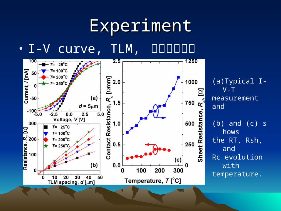
ExperimentExperiment• I-V curve, TLM, 接觸電阻結果
(a) Typical I-V-T measurement and
(b) and (c) showsthe RT, Rsh, and Rc evolution with temperature.
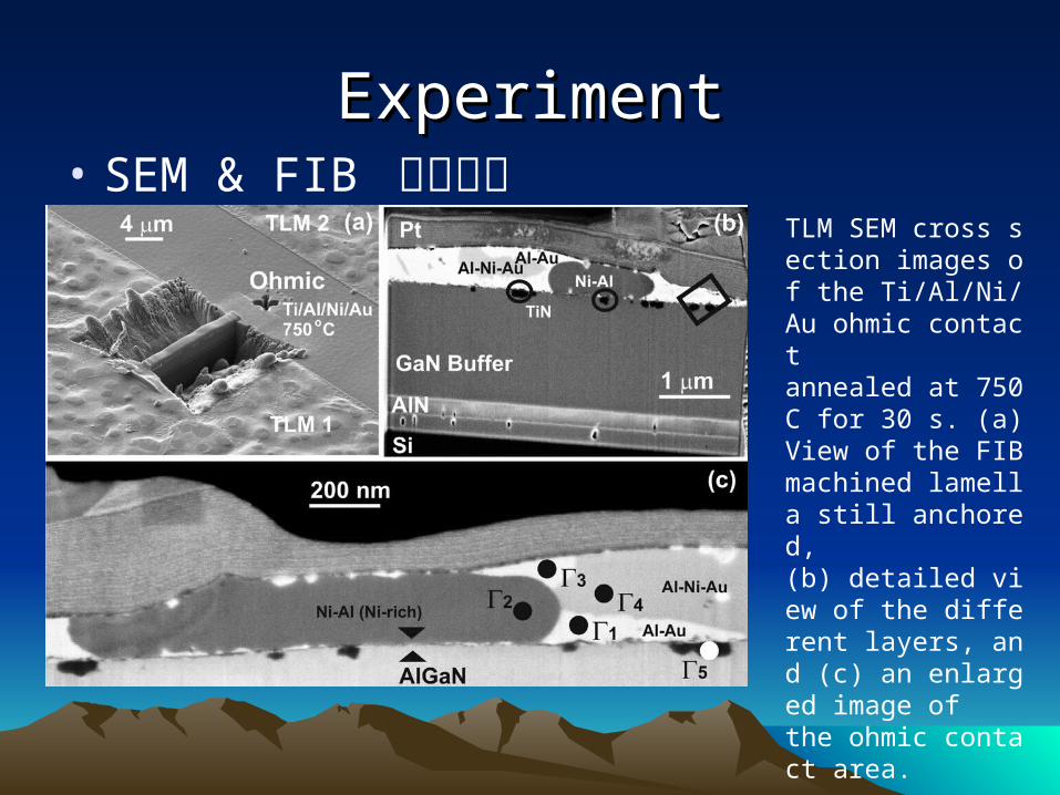
ExperimentExperiment• SEM & FIB 量測結果
TLM SEM cross section images of the Ti/Al/Ni/Au ohmic contactannealed at 750 C for 30 s. (a) View of the FIB machined lamella still anchored,(b) detailed view of the different layers, and (c) an enlarged image ofthe ohmic contact area.
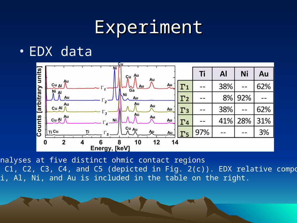
ExperimentExperiment• EDX data
EDX analyses at five distinct ohmic contact regionsnamed C1, C2, C3, C4, and C5 (depicted in Fig. 2(c)). EDX relative compositionfor Ti, Al, Ni, and Au is included in the table on the right.
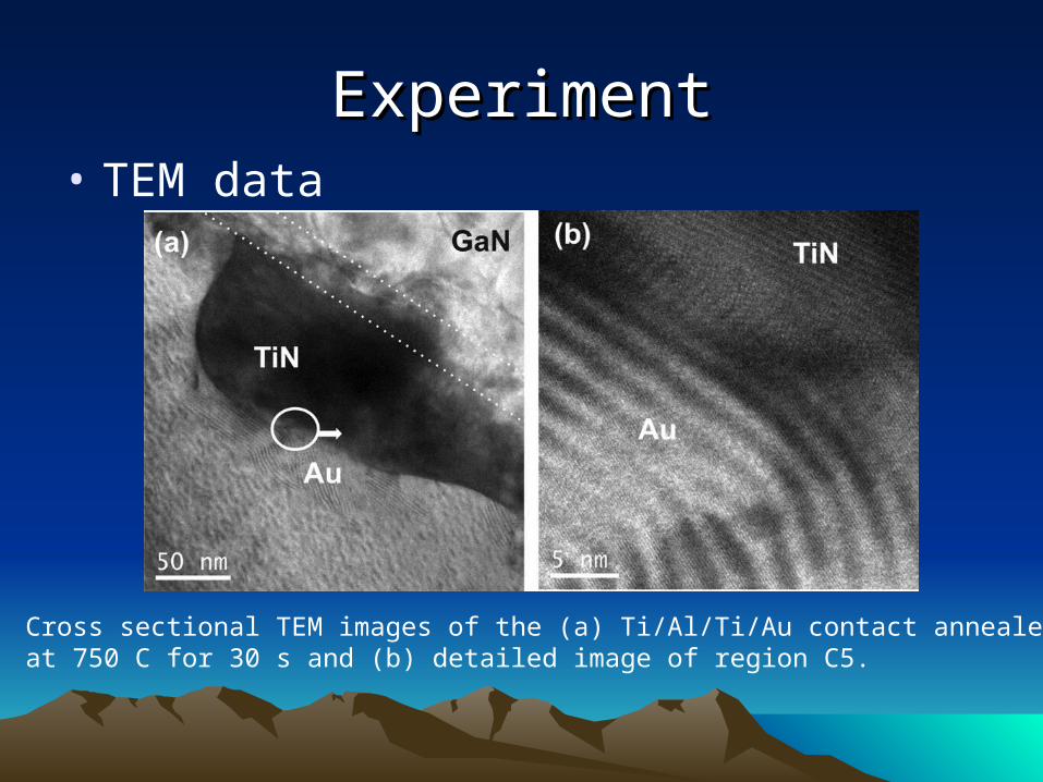
ExperimentExperiment• TEM data
Cross sectional TEM images of the (a) Ti/Al/Ti/Au contact annealedat 750 C for 30 s and (b) detailed image of region C5.
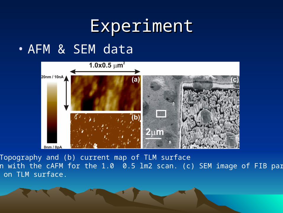
ExperimentExperiment• AFM & SEM data
(a) Topography and (b) current map of TLM surfacetaken with the cAFM for the 1.0 0.5 lm2 scan. (c) SEM image of FIB partialetch on TLM surface.
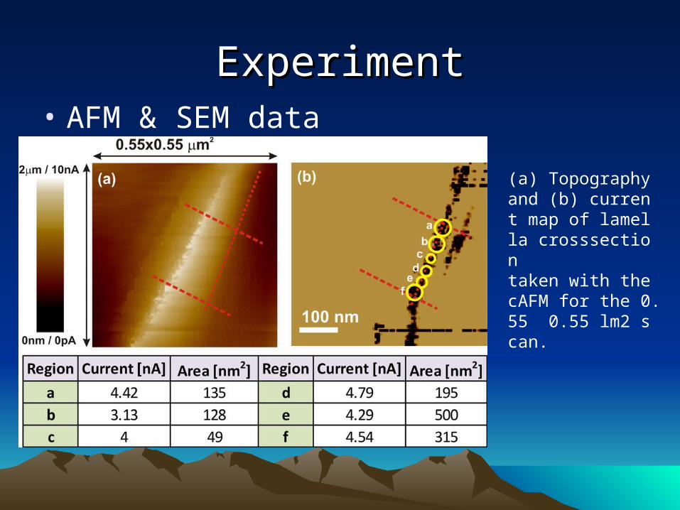
ExperimentExperiment• AFM & SEM data
(a) Topography and (b) current map of lamella crosssectiontaken with the cAFM for the 0.55 0.55 lm2 scan.
ConclusionConclusion
The submicron features of a typical Ti/Al/Ni/Au ohmic
contact to AlGaN/GaN, with reduced Rc of 0.2X mm, have
been investigated in detail. This included TLM vs T, in the temperature range of 25
C–300 C and a range of physical analysis tools like SEM,
FIB, TEM, and cAFM. The results suggest that the preferential contact
Mechanism is a direct electron path between the electrons
of the 2DEG and the metal stack, though only a small part
of the contact is actually conducting.

Thanks for your attentionThanks for your attention