Embed Size (px)
Citation preview
Micro/Nanolithography
©2013 Dale E. Ewbank
page 1 Micro/Nanolithography
Dale E. Ewbank
unL081413_microe.ppt
OUTLINE
Micro/Nanolithography ©2009 Dale E. Ewbank
page 2
Micro/Nanolithography
Masks
Optical Lithography
Photoresist
Sensitivity
Processing
Exposure Tools
Advanced Processes
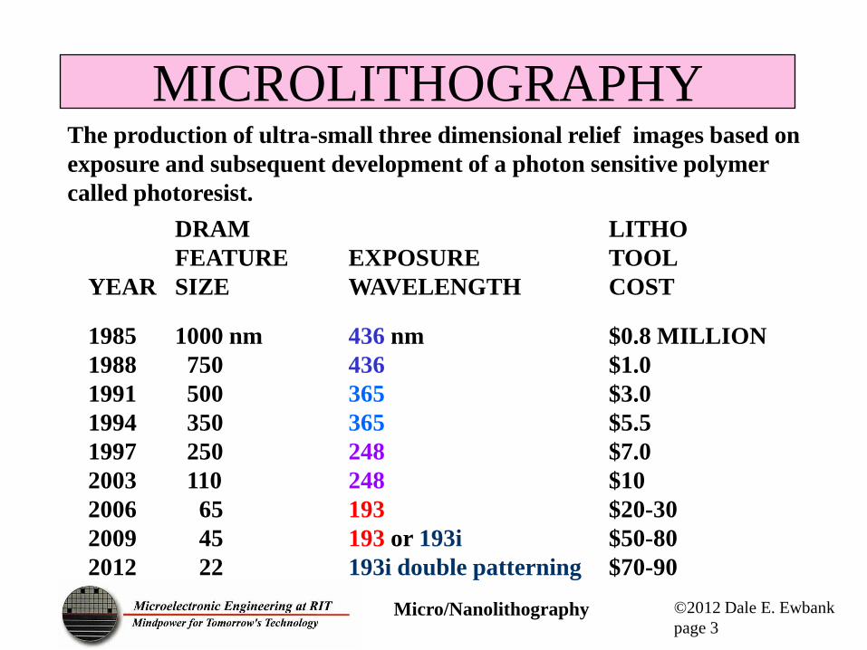
MICROLITHOGRAPHY
Micro/Nanolithography ©2012 Dale E. Ewbank
page 3
DRAM LITHO
FEATURE EXPOSURE TOOL
YEAR SIZE WAVELENGTH COST
1985 1000 nm 436 nm $0.8 MILLION
1988 750 436 $1.0
1991 500 365 $3.0
1994 350 365 $5.5
1997 250 248 $7.0
2003 110 248 $10
2006 65 193 $20-30
2009 45 193 or 193i $50-80
2012 22 193i double patterning $70-90
The production of ultra-small three dimensional relief images based on
exposure and subsequent development of a photon sensitive polymer
called photoresist.
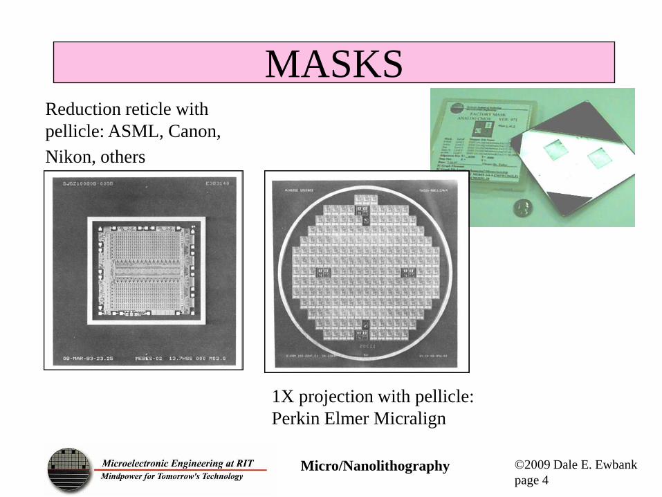
MASKS
Micro/Nanolithography ©2009 Dale E. Ewbank
page 4
Reduction reticle with
pellicle: ASML, Canon,
Nikon, others
1X projection with pellicle:
Perkin Elmer Micralign
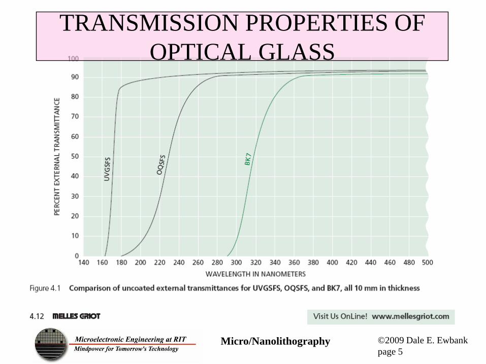
TRANSMISSION PROPERTIES OF
OPTICAL GLASS
Micro/Nanolithography ©2009 Dale E. Ewbank
page 5
Micro/Nanolithography ©2009 Dale E. Ewbank
page 6
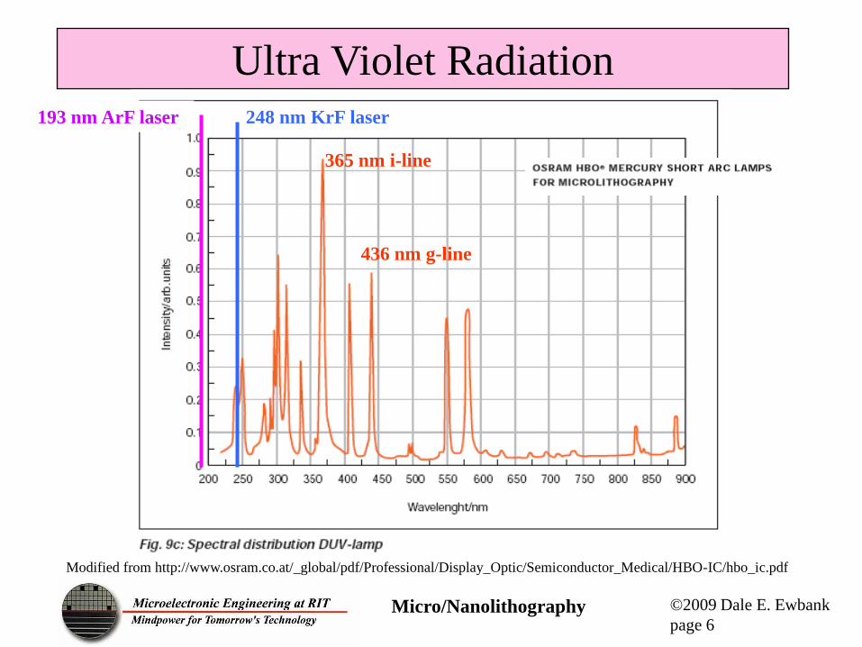
Ultra Violet Radiation Ultra Violet Radiation 248 nm KrF laser 193 nm ArF laser
365 nm i-line
436 nm g-line
Modified from http://www.osram.co.at/_global/pdf/Professional/Display_Optic/Semiconductor_Medical/HBO-IC/hbo_ic.pdf
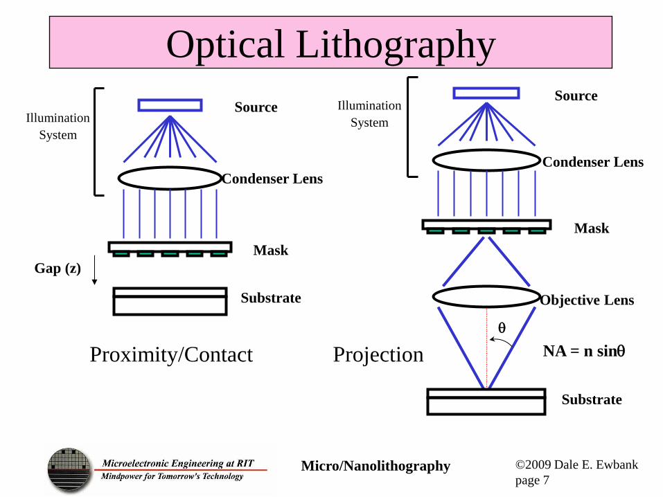
Optical Lithography
Micro/Nanolithography ©2009 Dale E. Ewbank
page 7
Illumination
System
Source
Condenser Lens
Mask
Objective Lens
Substrate
Illumination
System
Source
Condenser Lens
Mask
Substrate
Gap (z)
Proximity/Contact Projection NA = n sinq
q
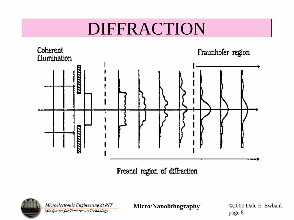
DIFFRACTION
Micro/Nanolithography ©2009 Dale E. Ewbank
page 8
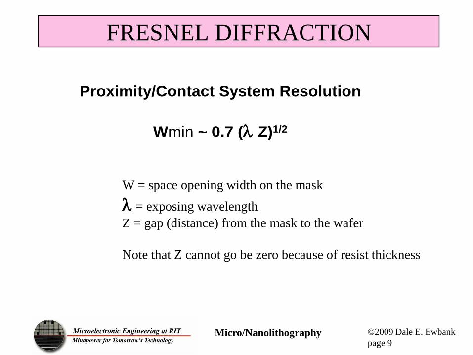
FRESNEL DIFFRACTION
Micro/Nanolithography ©2009 Dale E. Ewbank
page 9
Proximity/Contact System Resolution
Wmin ~ 0.7 ( Z)1/2
W = space opening width on the mask
= exposing wavelength
Z = gap (distance) from the mask to the wafer
Note that Z cannot go be zero because of resist thickness
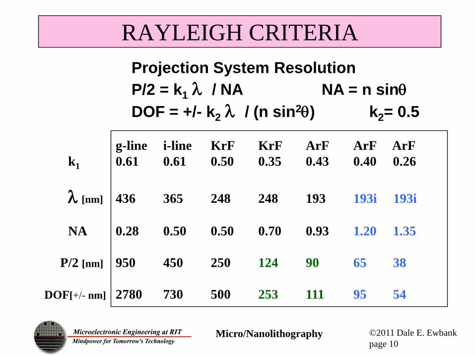
RAYLEIGH CRITERIA
Micro/Nanolithography ©2011 Dale E. Ewbank
page 10
Projection System Resolution
P/2 = k1 / NA NA = n sinq
DOF = +/- k2 / (n sin2q) k2= 0.5
g-line i-line KrF KrF ArF ArF ArF
k1 0.61 0.61 0.50 0.35 0.43 0.40 0.26
[nm] 436 365 248 248 193 193i 193i
NA 0.28 0.50 0.50 0.70 0.93 1.20 1.35
P/2 [nm] 950 450 250 124 90 65 38
DOF[+/- nm] 2780 730 500 253 111 95 54
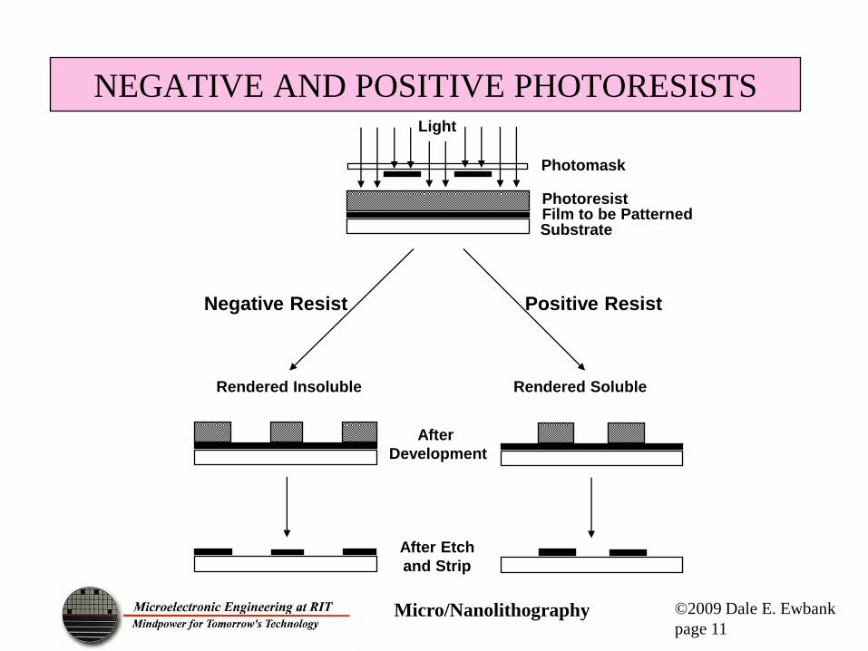
NEGATIVE AND POSITIVE PHOTORESISTS
Micro/Nanolithography ©2009 Dale E. Ewbank
page 11
Photomask
Photoresist Film to be Patterned Substrate
Light
Negative Resist Positive Resist
Rendered Insoluble Rendered Soluble
After
Development
After Etch
and Strip
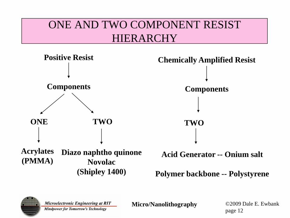
ONE AND TWO COMPONENT RESIST
HIERARCHY
Micro/Nanolithography ©2009 Dale E. Ewbank
page 12
Positive Resist
Components
Acrylates
(PMMA)
ONE TWO
Diazo naphtho quinone
Novolac
(Shipley 1400)
Acid Generator -- Onium salt
Polymer backbone -- Polystyrene
TWO
Chemically Amplified Resist
Components
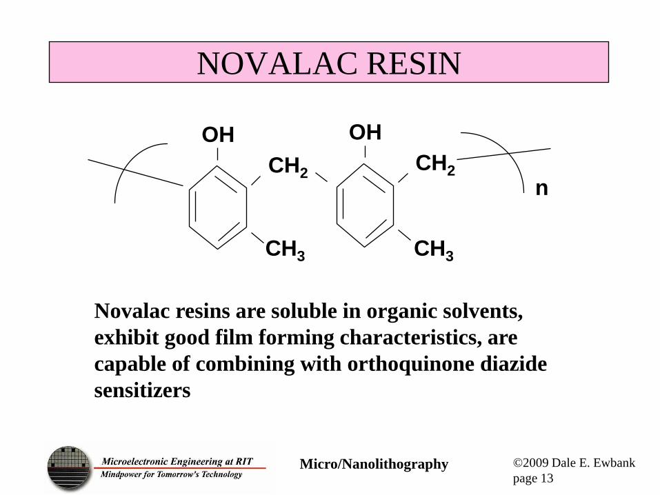
NOVALAC RESIN
Micro/Nanolithography ©2009 Dale E. Ewbank
page 13
Novalac resins are soluble in organic solvents,
exhibit good film forming characteristics, are
capable of combining with orthoquinone diazide
sensitizers
CH2
OH
CH3
CH2
OH
CH3
n
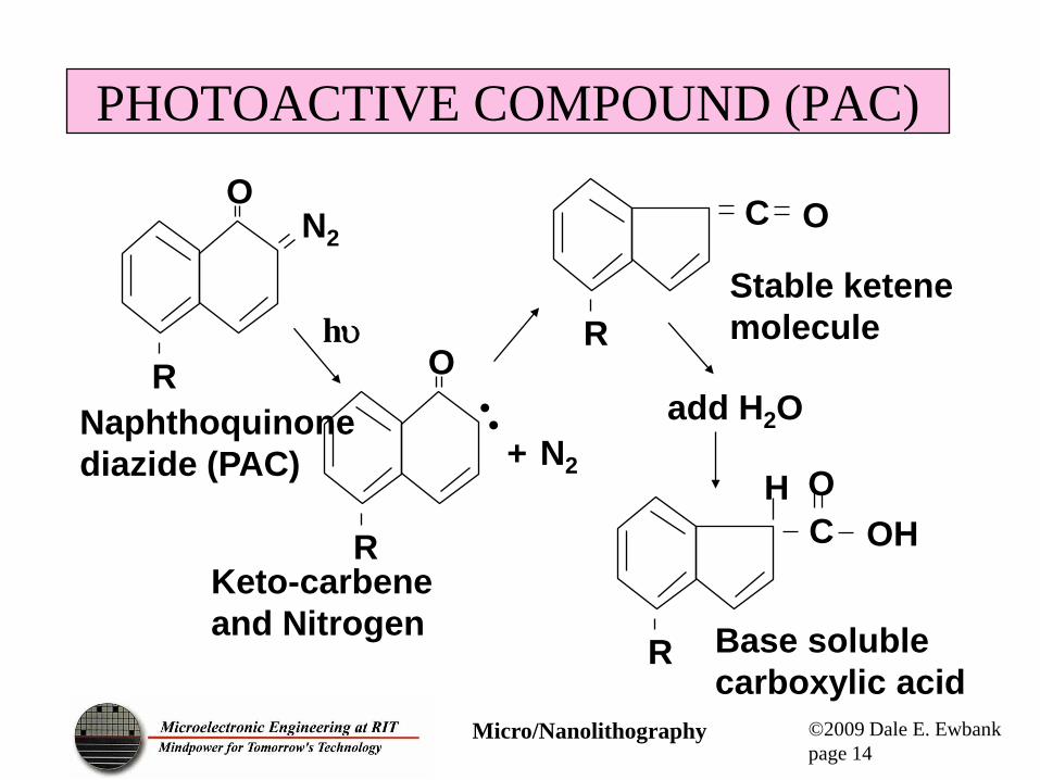
PHOTOACTIVE COMPOUND (PAC)
Micro/Nanolithography ©2009 Dale E. Ewbank
page 14
Naphthoquinone
diazide (PAC)
N2
O
R
N2
O
R
+
Keto-carbene
and Nitrogen
Stable ketene
molecule
O
R
C
OH
R
C
O H
Base soluble
carboxylic acid
add H2O
hu
• •
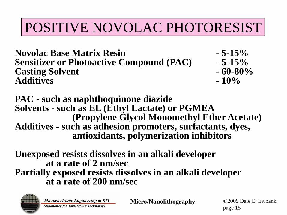
POSITIVE NOVOLAC PHOTORESIST
Micro/Nanolithography ©2009 Dale E. Ewbank
page 15
Novolac Base Matrix Resin - 5-15% Sensitizer or Photoactive Compound (PAC) - 5-15% Casting Solvent - 60-80% Additives - 10% PAC - such as naphthoquinone diazide Solvents - such as EL (Ethyl Lactate) or PGMEA (Propylene Glycol Monomethyl Ether Acetate) Additives - such as adhesion promoters, surfactants, dyes, antioxidants, polymerization inhibitors Unexposed resists dissolves in an alkali developer at a rate of 2 nm/sec Partially exposed resists dissolves in an alkali developer at a rate of 200 nm/sec
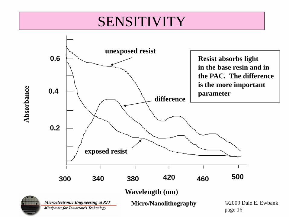
SENSITIVITY
Micro/Nanolithography ©2009 Dale E. Ewbank
page 16
500 460 380 340 300 420
Wavelength (nm)
unexposed resist
exposed resist
difference
Ab
sorb
an
ce
0.2
0.4
0.6 Resist absorbs light
in the base resin and in
the PAC. The difference
is the more important
parameter
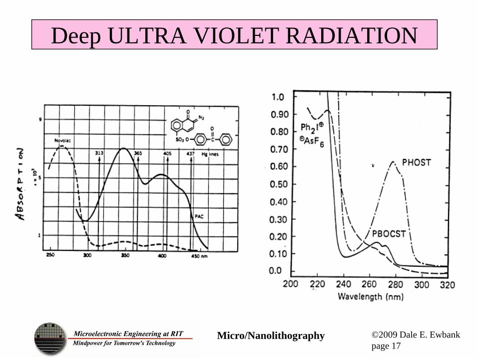
Deep ULTRA VIOLET RADIATION
Micro/Nanolithography ©2009 Dale E. Ewbank
page 17
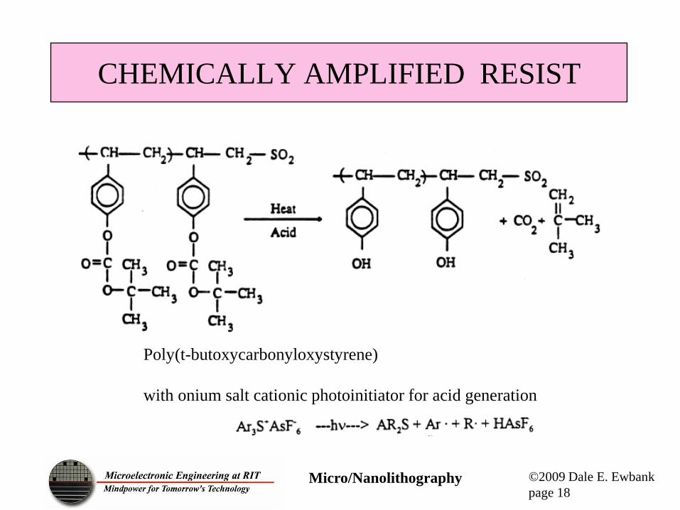
CHEMICALLY AMPLIFIED RESIST
Micro/Nanolithography ©2009 Dale E. Ewbank
page 18
Poly(t-butoxycarbonyloxystyrene)
with onium salt cationic photoinitiator for acid generation
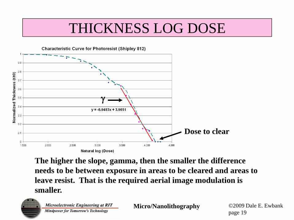
THICKNESS LOG DOSE
Micro/Nanolithography ©2009 Dale E. Ewbank
page 19
g
Dose to clear
The higher the slope, gamma, then the smaller the difference
needs to be between exposure in areas to be cleared and areas to
leave resist. That is the required aerial image modulation is
smaller.
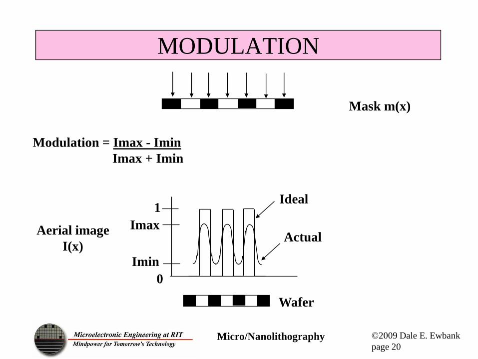
MODULATION
Micro/Nanolithography ©2009 Dale E. Ewbank
page 20
Aerial image
I(x)
Wafer
Mask m(x)
Modulation = Imax - Imin
Imax + Imin
Imax
Imin
1
0
Actual
Ideal
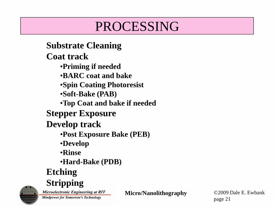
PROCESSING
Micro/Nanolithography ©2009 Dale E. Ewbank
page 21
Substrate Cleaning
Coat track •Priming if needed
•BARC coat and bake
•Spin Coating Photoresist
•Soft-Bake (PAB)
•Top Coat and bake if needed
Stepper Exposure
Develop track •Post Exposure Bake (PEB)
•Develop
•Rinse
•Hard-Bake (PDB)
Etching
Stripping
SUBSTRATE CLEAN AND PRIME
Micro/Nanolithography ©2009 Dale E. Ewbank
page 22
Cleaning is done with a high pressure (2000 psi) water scrub A dehydration bake is typically done on a hot plate at 250 °C for 1 min. (Wafers are clean and dry just after removing from oxide growth furnace) HMDS (hexa-methyl-di-silizane), - Adhesion promoter or primer: Are commonly applied as a liquid or vapor. HMDS attaches to remaining OH molecules releasing ammonia gas and creating an organic-like surface improving adhesion Too much HMDS is detrimental to sensitivity and adhesion.
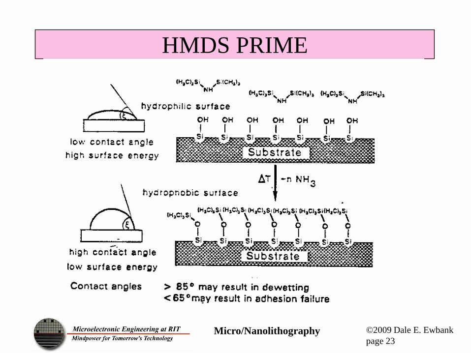
HMDS PRIME
Micro/Nanolithography ©2009 Dale E. Ewbank
page 23
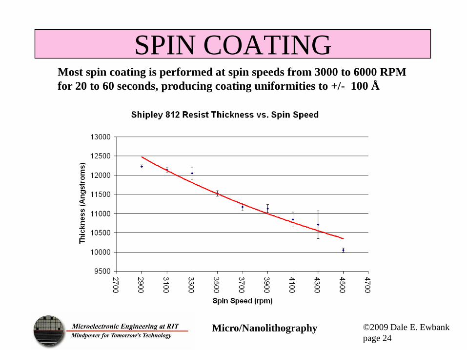
SPIN COATING
Micro/Nanolithography ©2009 Dale E. Ewbank
page 24
Most spin coating is performed at spin speeds from 3000 to 6000 RPM
for 20 to 60 seconds, producing coating uniformities to +/- 100 Å
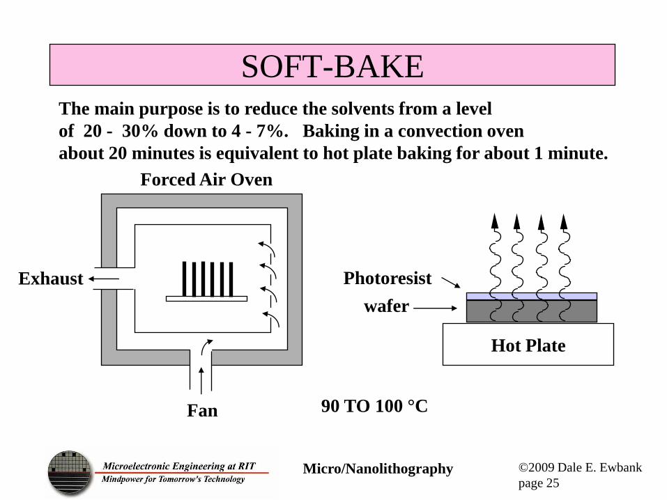
SOFT-BAKE
Micro/Nanolithography ©2009 Dale E. Ewbank
page 25
The main purpose is to reduce the solvents from a level
of 20 - 30% down to 4 - 7%. Baking in a convection oven
about 20 minutes is equivalent to hot plate baking for about 1 minute.
Hot Plate
Exhaust Photoresist
wafer
Forced Air Oven
Fan 90 TO 100 °C
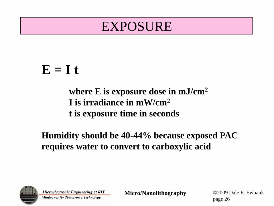
EXPOSURE
Micro/Nanolithography ©2009 Dale E. Ewbank
page 26
E = I t
where E is exposure dose in mJ/cm2
I is irradiance in mW/cm2
t is exposure time in seconds
Humidity should be 40-44% because exposed PAC
requires water to convert to carboxylic acid
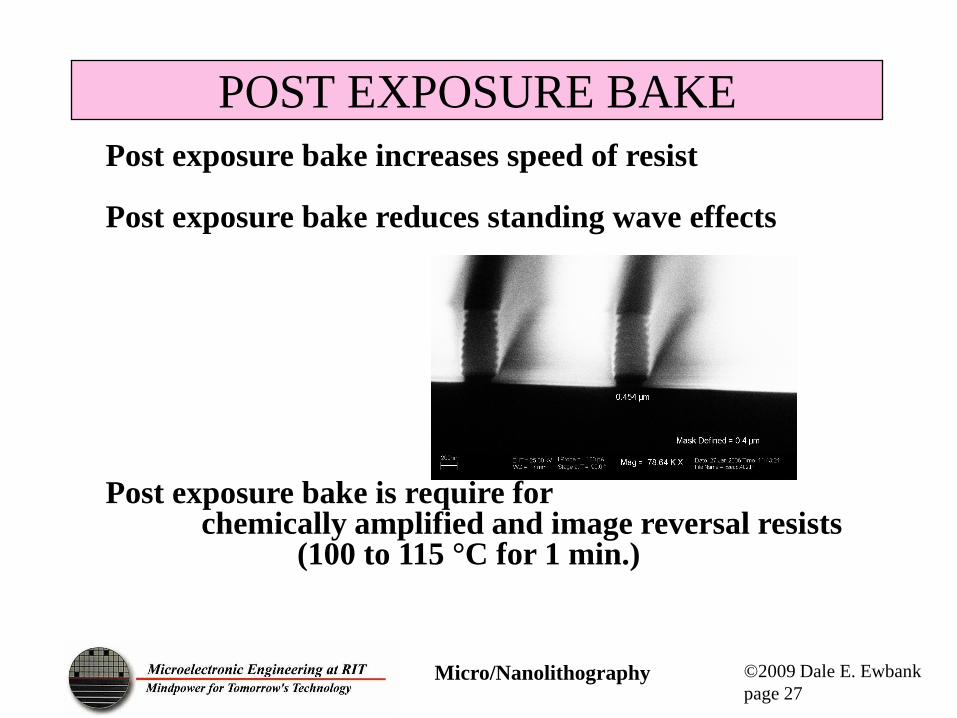
POST EXPOSURE BAKE
Micro/Nanolithography ©2009 Dale E. Ewbank
page 27
Post exposure bake increases speed of resist Post exposure bake reduces standing wave effects Post exposure bake is require for chemically amplified and image reversal resists (100 to 115 °C for 1 min.)
DEVELOP AND RINSE
Micro/Nanolithography ©2009 Dale E. Ewbank
page 28
Develop is done in an alkali solution such as NaOH or
KOH (Metal Containing Developers) Trace quantities
of these metals can cause transistor threshold voltage
shifts.
Metal Ion Free Developers are available (TMAH)
Developer Concentration and Temperature of
Developer are the most important parameters to
control.
HARD BAKE
Micro/Nanolithography ©2009 Dale E. Ewbank
page 29
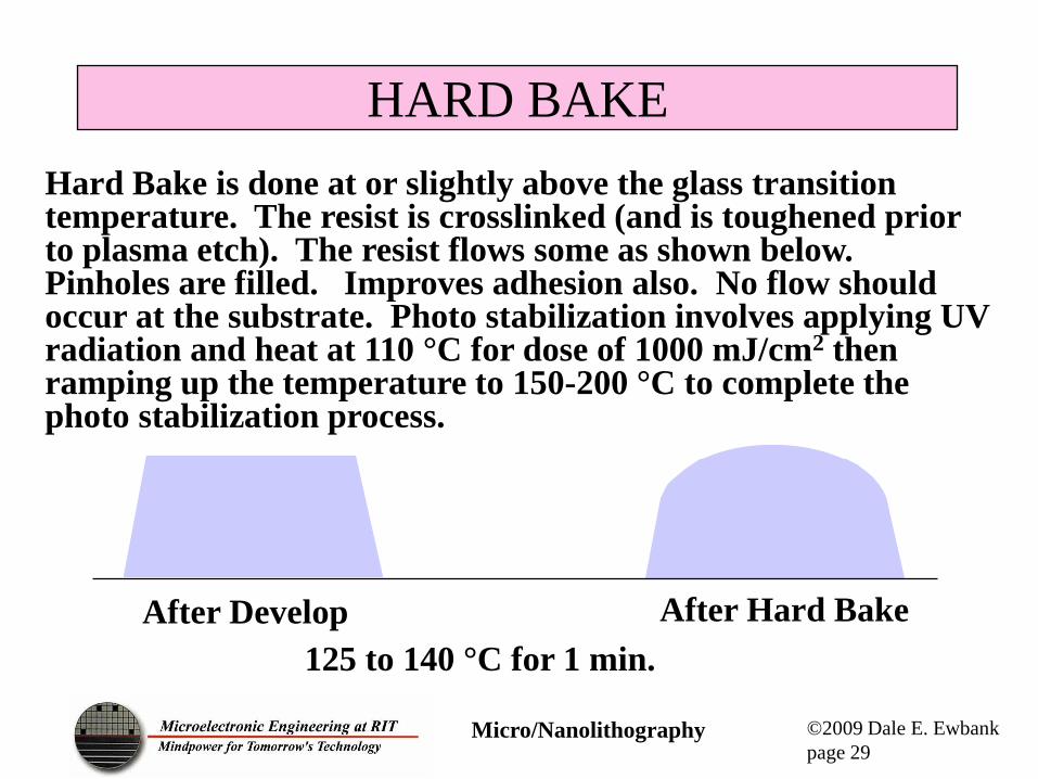
Hard Bake is done at or slightly above the glass transition temperature. The resist is crosslinked (and is toughened prior to plasma etch). The resist flows some as shown below. Pinholes are filled. Improves adhesion also. No flow should occur at the substrate. Photo stabilization involves applying UV radiation and heat at 110 °C for dose of 1000 mJ/cm2 then ramping up the temperature to 150-200 °C to complete the photo stabilization process.
After Develop After Hard Bake
125 to 140 °C for 1 min.
ETCHING
Micro/Nanolithography ©2009 Dale E. Ewbank
page 30
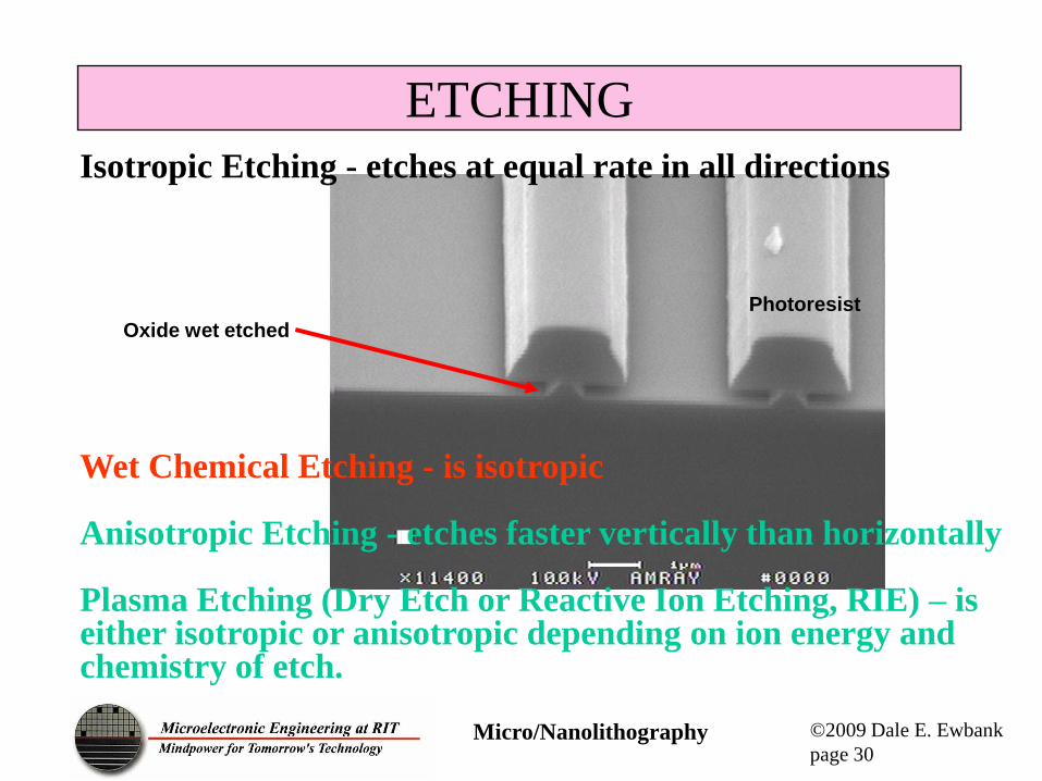
Isotropic Etching - etches at equal rate in all directions Wet Chemical Etching - is isotropic Anisotropic Etching - etches faster vertically than horizontally Plasma Etching (Dry Etch or Reactive Ion Etching, RIE) – is either isotropic or anisotropic depending on ion energy and chemistry of etch.
Oxide wet etched
Photoresist
STRIPPING
Micro/Nanolithography ©2009 Dale E. Ewbank
page 31
Oxygen Plasma Ashing
Plasma Damage is Possible to sensitive gate oxide layers
Hot Sulfuric Acid and Hydrogen Peroxide
If underlying layers are not etched by these chemicals
Organic Solvents are available
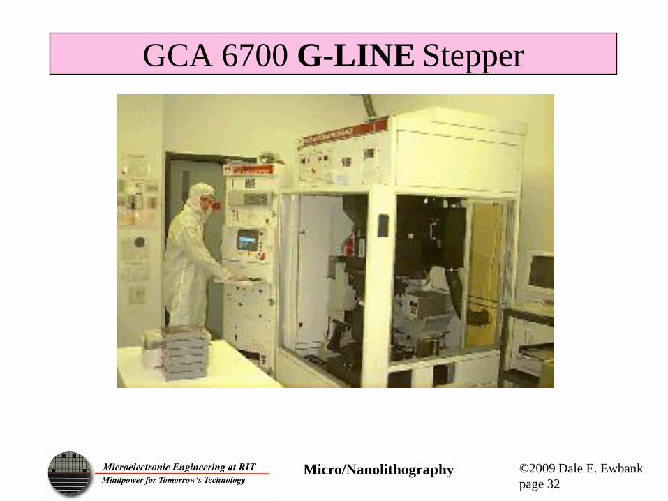
GCA 6700 G-LINE Stepper
Micro/Nanolithography ©2009 Dale E. Ewbank
page 32
Microlithography ©2011 Dale E. Ewbank
page 33
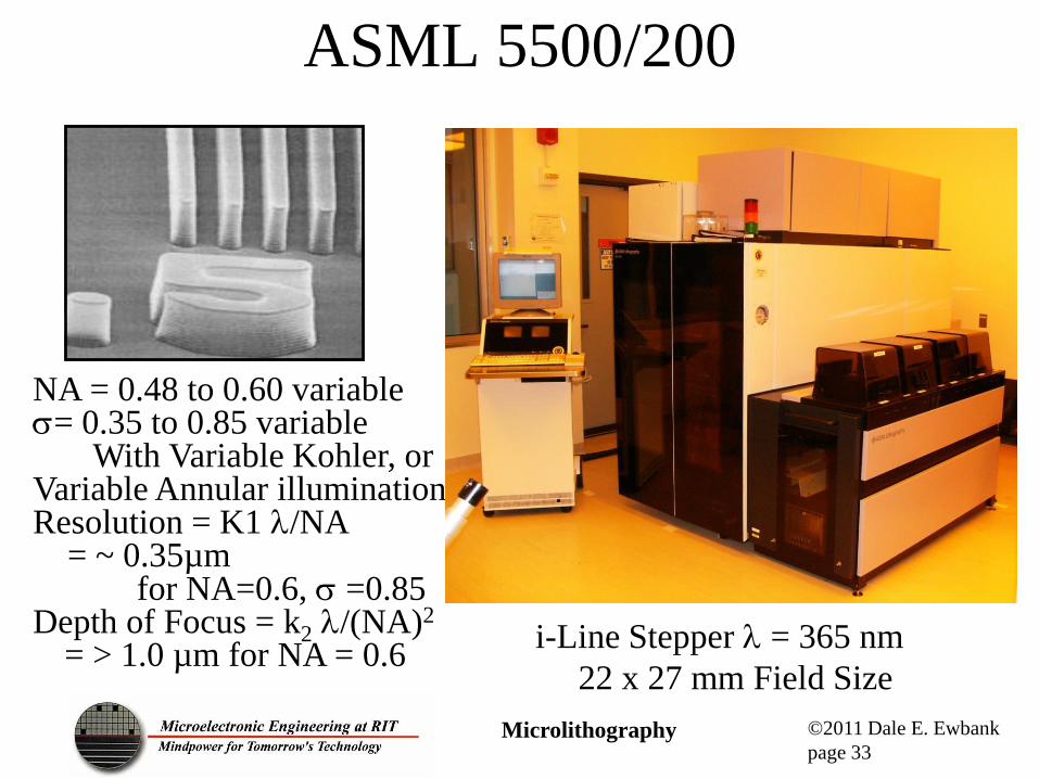
ASML 5500/200
NA = 0.48 to 0.60 variable = 0.35 to 0.85 variable With Variable Kohler, or Variable Annular illumination Resolution = K1 /NA = ~ 0.35µm for NA=0.6, =0.85 Depth of Focus = k2 /(NA)2
= > 1.0 µm for NA = 0.6 i-Line Stepper = 365 nm
22 x 27 mm Field Size
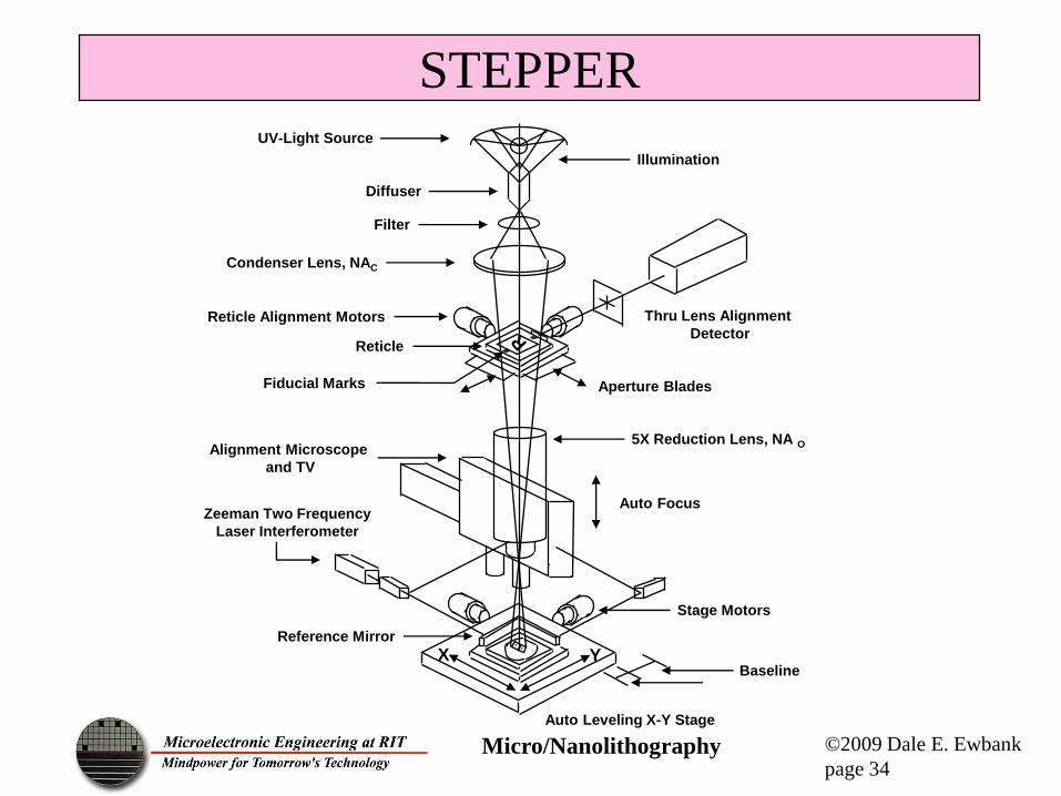
STEPPER
Micro/Nanolithography ©2009 Dale E. Ewbank
page 34
X Y
UV-Light Source
Diffuser
Condenser Lens, NAC
Filter
Reticle Alignment Motors Thru Lens Alignment
Detector
Illumination
Reticle
5X Reduction Lens, NA O
Auto Focus
Aperture Blades
Baseline
Stage Motors
Auto Leveling X-Y Stage
Reference Mirror
Alignment Microscope
and TV
Zeeman Two Frequency
Laser Interferometer
Fiducial Marks
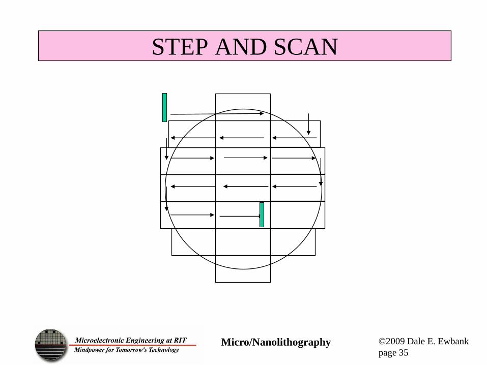
STEP AND SCAN
Micro/Nanolithography ©2009 Dale E. Ewbank
page 35
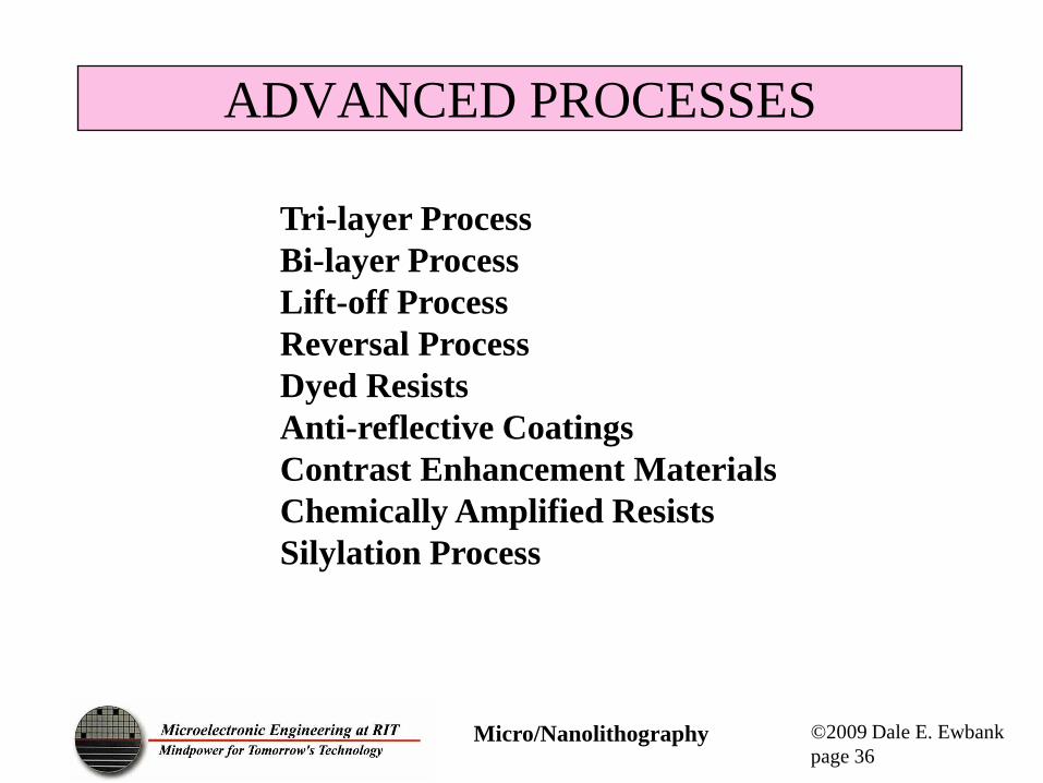
ADVANCED PROCESSES
Micro/Nanolithography ©2009 Dale E. Ewbank
page 36
Tri-layer Process
Bi-layer Process
Lift-off Process
Reversal Process
Dyed Resists
Anti-reflective Coatings
Contrast Enhancement Materials
Chemically Amplified Resists
Silylation Process
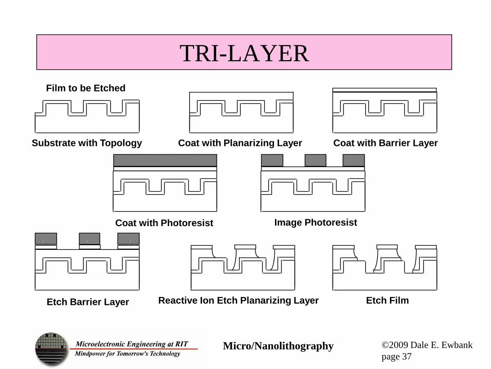
TRI-LAYER
Micro/Nanolithography ©2009 Dale E. Ewbank
page 37
Substrate with Topology
Film to be Etched
Coat with Planarizing Layer Coat with Barrier Layer
Coat with Photoresist Image Photoresist
Etch Barrier Layer Reactive Ion Etch Planarizing Layer Etch Film
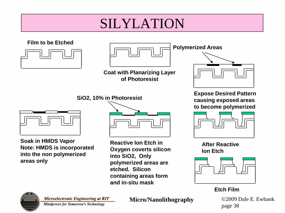
SILYLATION
Micro/Nanolithography ©2009 Dale E. Ewbank
page 38
Film to be Etched
Expose Desired Pattern
causing exposed areas
to become polymerized
Coat with Planarizing Layer
of Photoresist
After Reactive
Ion Etch
Etch Film
Polymerized Areas
Soak in HMDS Vapor
Note: HMDS is incorporated
into the non polymerized
areas only
Reactive Ion Etch in
Oxygen coverts silicon
into SiO2, Only
polymerized areas are
etched. Silicon
containing areas form
and in-situ mask
SiO2, 10% in Photoresist
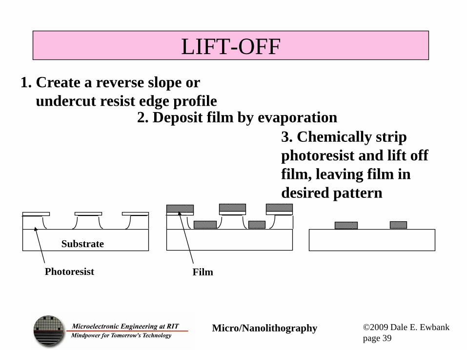
LIFT-OFF
Micro/Nanolithography ©2009 Dale E. Ewbank
page 39
1. Create a reverse slope or
undercut resist edge profile 2. Deposit film by evaporation
3. Chemically strip
photoresist and lift off
film, leaving film in
desired pattern
Substrate
Photoresist Film
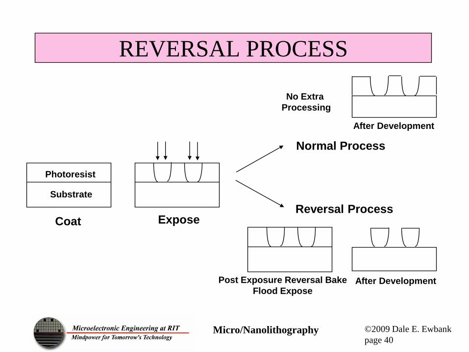
REVERSAL PROCESS
Micro/Nanolithography ©2009 Dale E. Ewbank
page 40
Coat
Photoresist
Substrate
Expose
Normal Process
No Extra
Processing
Reversal Process
Post Exposure Reversal Bake
Flood Expose After Development
After Development
REFERENCES
• Microlithography Science and Technology, Second Edition, edited by Kazuaki Suzuki and
Bruce W. Smith, CRC Press, 2007.
• Introduction to Micro/Nanolithography, Second Edition, Edited by Larry F. Thompson,
C.Grant Willson and Murrae J. Bowden, ACS Professional Reference Book, American
Chemical Society, Washington, DC 1994.
• Micro/Nanolithography, David Elliott, McGraw Hill Book Company, 1986.
• www.osram.co.at/_global/pdf/Professional/Display_Optic/Semiconductor_Medical/HBO-
IC/hbo_ic.pdf, accessed 03/13/2009.
• www.mellesgriot.com, accessed 06/10/2008.
• http://www.itrs.net/reports.html, accessed 03/14/2011.
Micro/Nanolithography ©2012 Dale E. Ewbank
page 41