Embed Size (px)
DESCRIPTION
Explains Overview about Rectangular and Circular Microstrip Antenna
Citation preview
Overview of Microstrip AntennasAlso called “patch antennas”
• One of the most useful antennas at microwave frequencies(f > 1 GHz).
• It consists of a metal “patch” on top of a grounded dielectric substrate.
• The patch may be in a variety of shapes, but rectangular and circular are the most common.
History of Microstrip Antennas
• Invented by Bob Munson in 1972.
• Became popular starting in the 1970s.
R. E. Munson, “Microstrip Phased Array Antennas,” Proc. of Twenty-Second Symp. on USAF Antenna Research and Development Program,October 1972.
R. E. Munson, “Conformal Microstrip Antennas and Microstrip Phased Arrays,” IEEE Trans. Antennas Propagat., vol. AP-22, no. 1 (January 1974): 74–78.
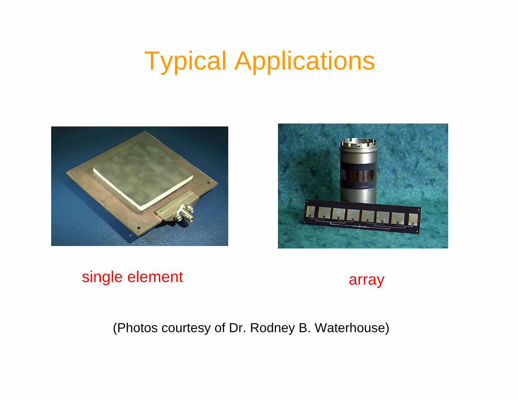
Typical Applications
single element array
(Photos courtesy of Dr. Rodney B. Waterhouse)
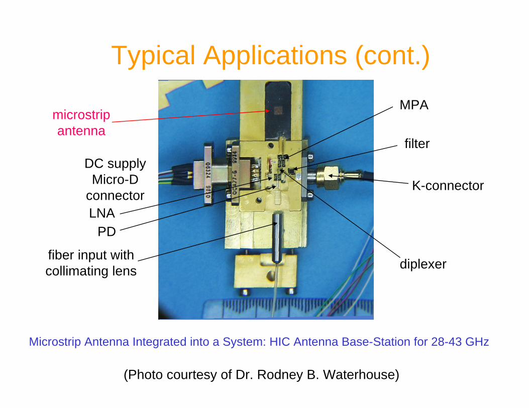
Typical Applications (cont.)
Microstrip Antenna Integrated into a System: HIC Antenna Base-Station for 28-43 GHz
filter
MPA
diplexer
LNAPD
K-connectorDC supply
Micro-D connector
microstrip antenna
fiber input with collimating lens
(Photo courtesy of Dr. Rodney B. Waterhouse)
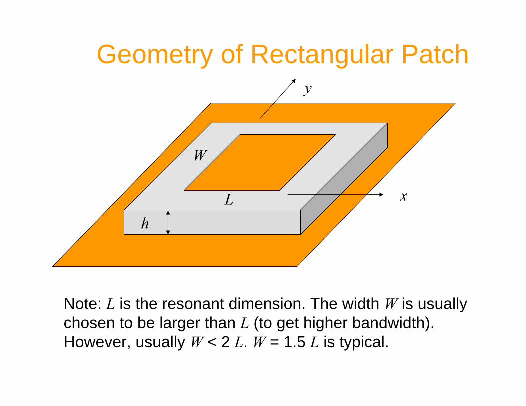
Geometry of Rectangular Patch
x
y
hL
W
Note: L is the resonant dimension. The width W is usually chosen to be larger than L (to get higher bandwidth). However, usually W < 2 L. W = 1.5 L is typical.
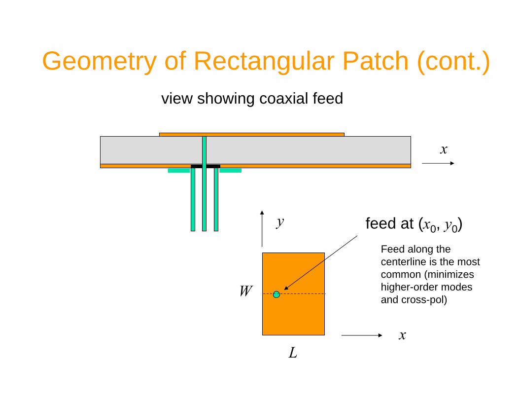
Geometry of Rectangular Patch (cont.)view showing coaxial feed
x
y
L
W
feed at (x0, y0)Feed along the centerline is the most common (minimizes higher-order modes and cross-pol)
x
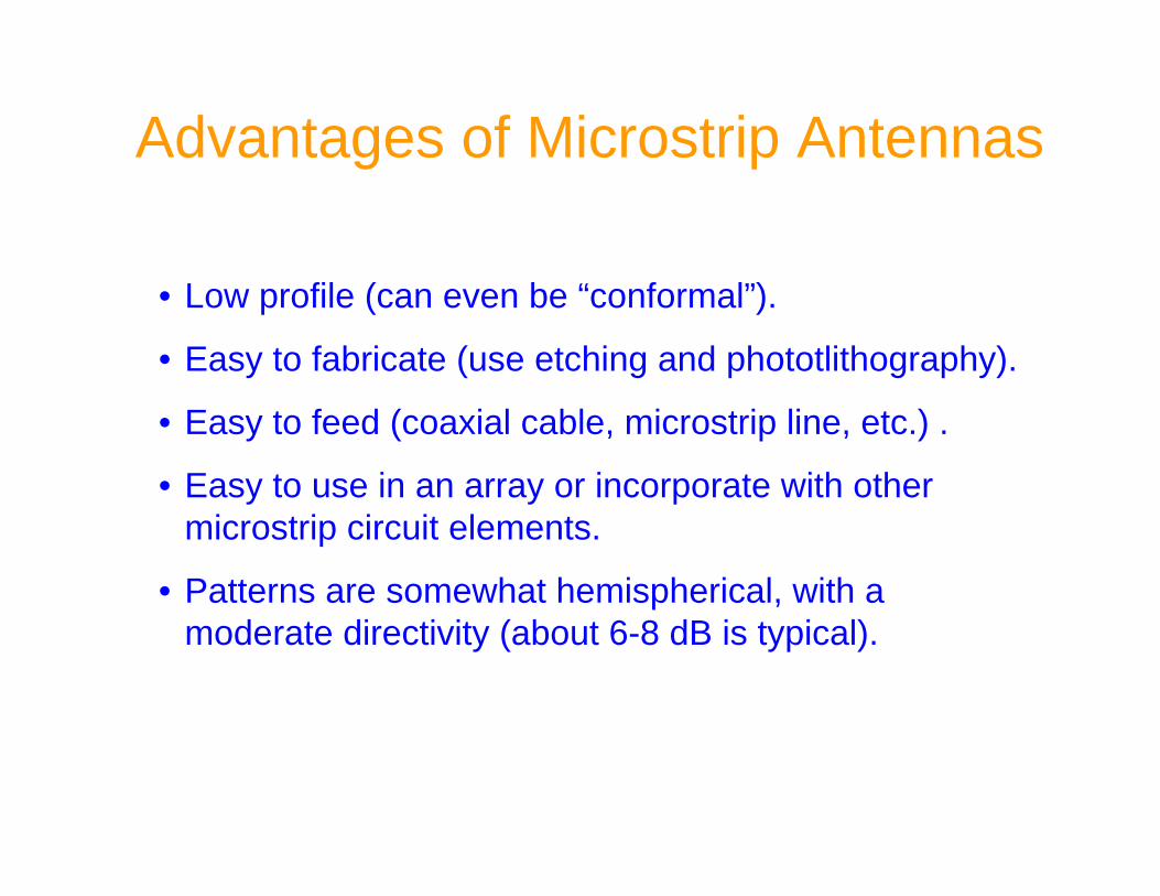
Advantages of Microstrip Antennas
• Low profile (can even be “conformal”).
• Easy to fabricate (use etching and phototlithography).
• Easy to feed (coaxial cable, microstrip line, etc.) .
• Easy to use in an array or incorporate with other microstrip circuit elements.
• Patterns are somewhat hemispherical, with a moderate directivity (about 6-8 dB is typical).
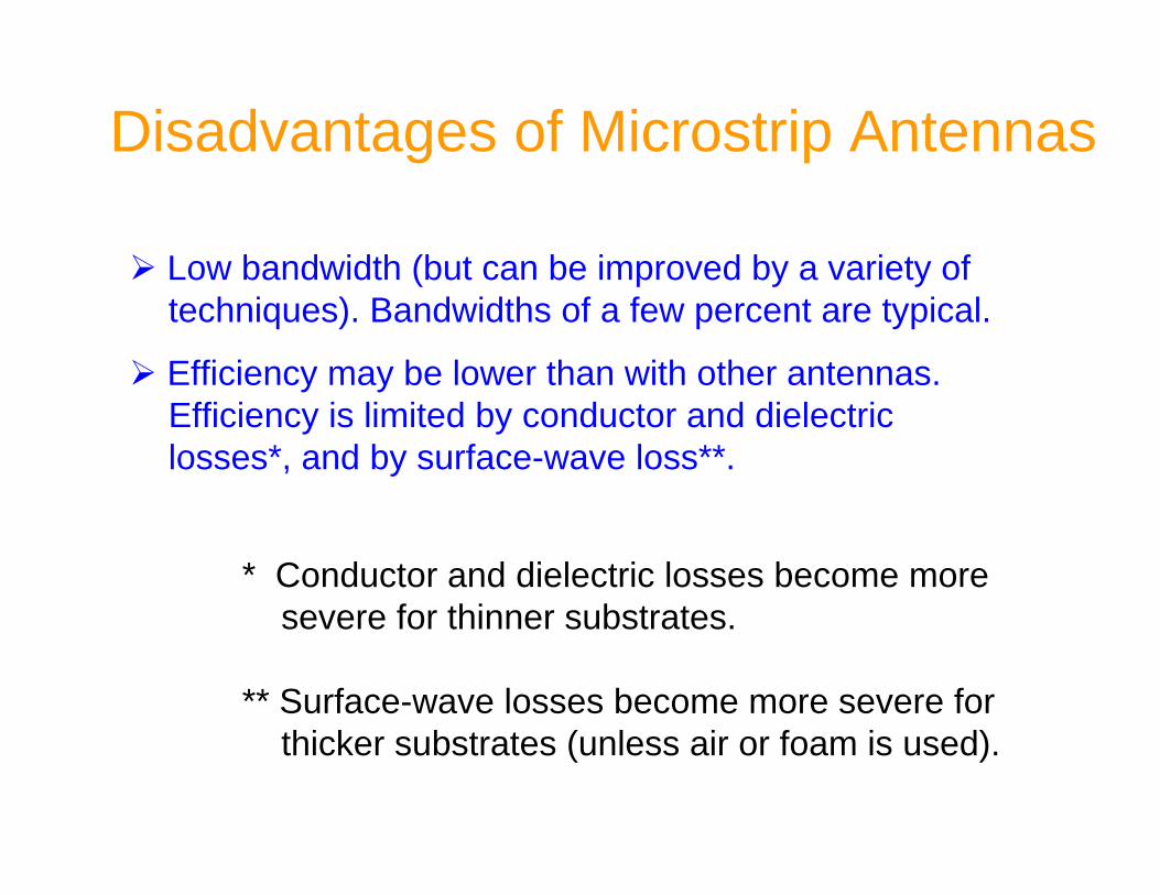
Disadvantages of Microstrip Antennas
Low bandwidth (but can be improved by a variety of techniques). Bandwidths of a few percent are typical.
Efficiency may be lower than with other antennas. Efficiency is limited by conductor and dielectric losses*, and by surface-wave loss**.
* Conductor and dielectric losses become more severe for thinner substrates.
** Surface-wave losses become more severe for thicker substrates (unless air or foam is used).
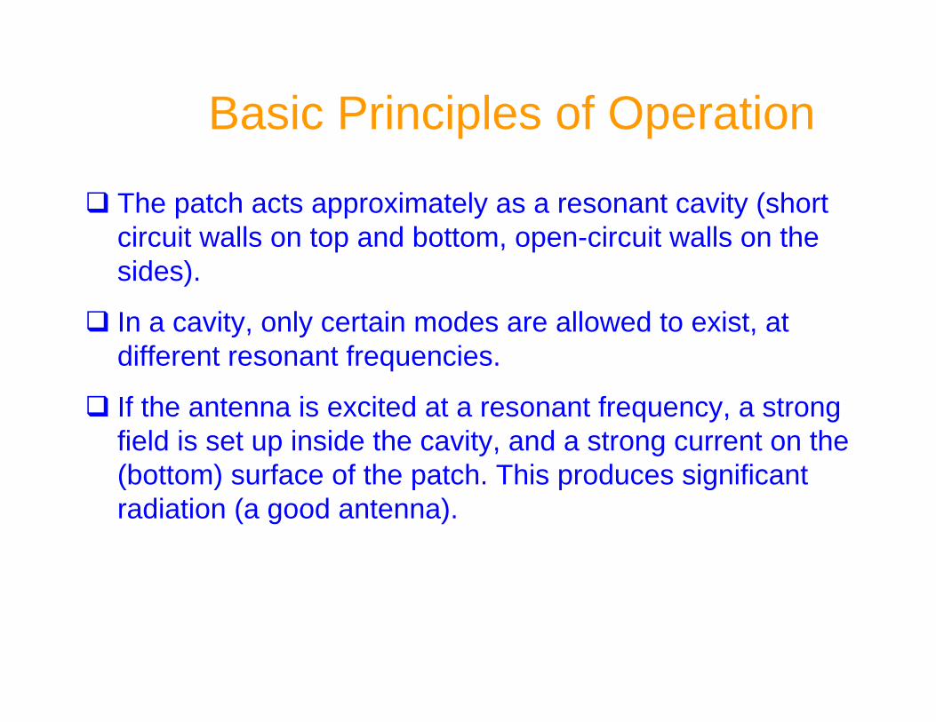
Basic Principles of Operation
The patch acts approximately as a resonant cavity (short circuit walls on top and bottom, open-circuit walls on the sides).
In a cavity, only certain modes are allowed to exist, at different resonant frequencies.
If the antenna is excited at a resonant frequency, a strong field is set up inside the cavity, and a strong current on the (bottom) surface of the patch. This produces significant radiation (a good antenna).
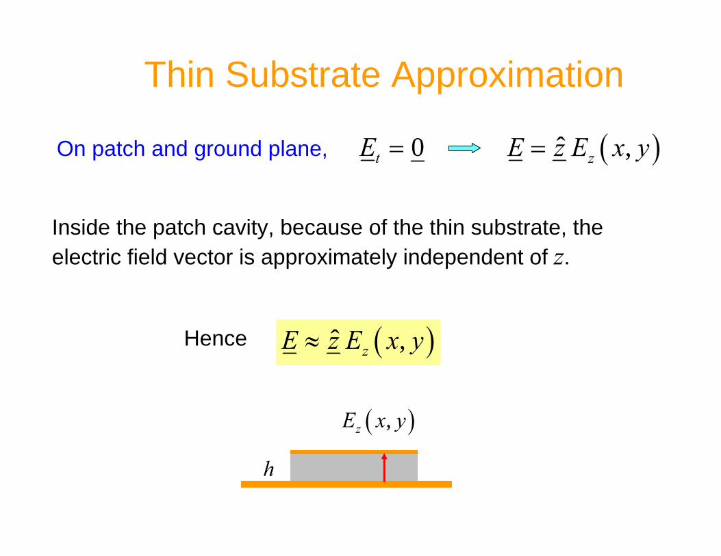
Thin Substrate Approximation
On patch and ground plane, 0tE = ( )ˆ ,zE z E x y=
Inside the patch cavity, because of the thin substrate, the electric field vector is approximately independent of z.
Hence ( )ˆ ,zE z E x y≈
h
( ),zE x y
Thin Substrate Approximation
( )( )
( )( )
1
1 ˆ ,
1 ˆ ,
z
z
H Ej
zE x yj
z E x yj
ωμ
ωμ
ωμ
= − ∇×
= − ∇×
= − − ×∇
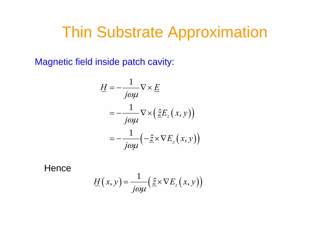
Magnetic field inside patch cavity:
( ) ( )( )1 ˆ, ,zH x y z E x yjωμ
= ×∇Hence
Thin Substrate Approximation (cont.)
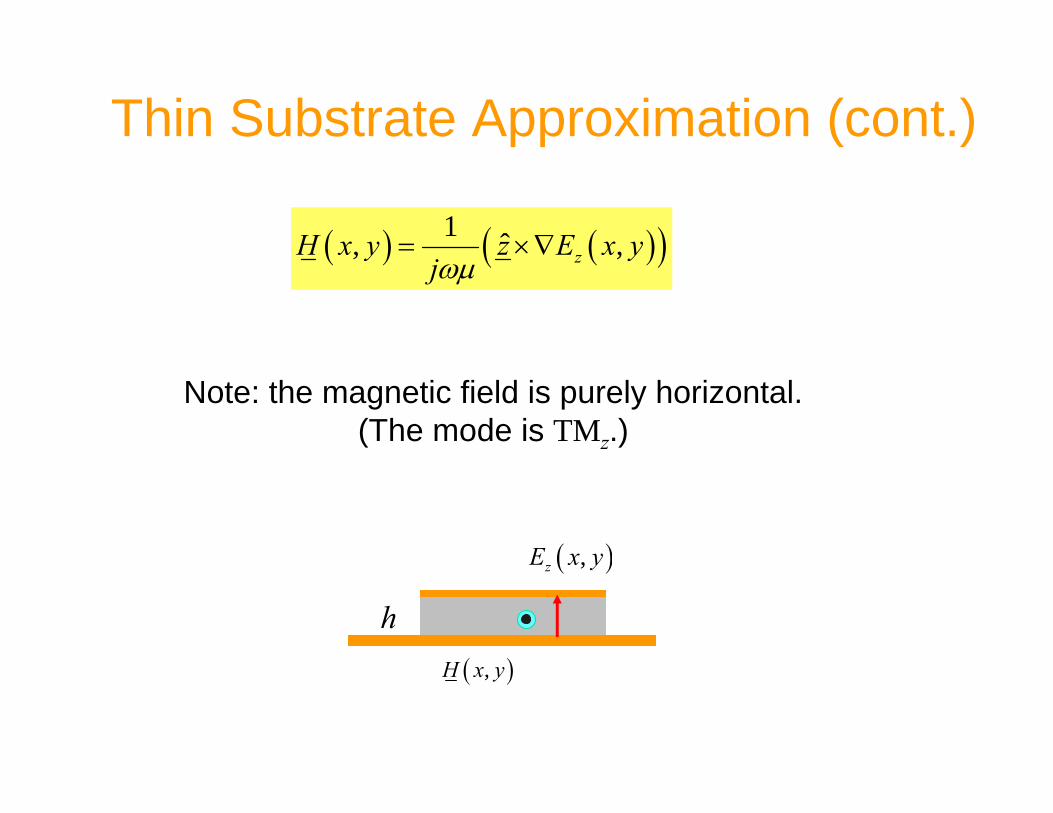
( ) ( )( )1 ˆ, ,zH x y z E x yjωμ
= ×∇
Note: the magnetic field is purely horizontal.(The mode is TMz.)
h
( ),zE x y
( ),H x y
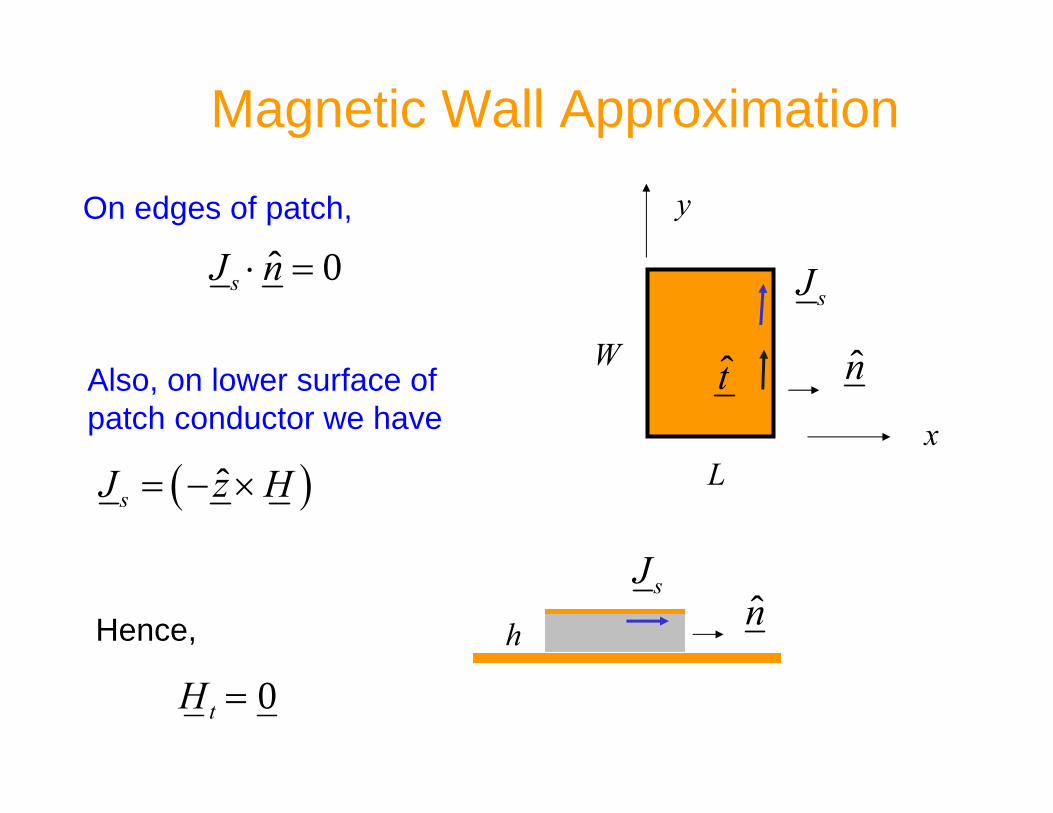
Magnetic Wall Approximation
On edges of patch,
ˆ 0sJ n⋅ =
n̂hsJ
( )ˆsJ z H= − ×
Hence,
0tH =
x
y
n̂
L
W
sJ
t̂Also, on lower surface of patch conductor we have
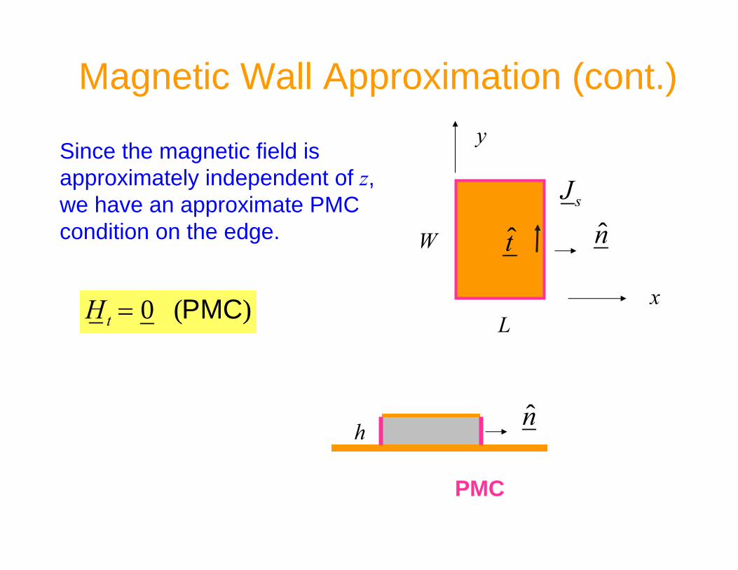
Magnetic Wall Approximation (cont.)
n̂h
x
y
n̂
L
W
sJ
t̂
0 ( )tH = PMC
Since the magnetic field is approximately independent of z, we have an approximate PMC condition on the edge.
PMC
n̂h
x
y
n̂
L
W
sJ
t̂Hence,
PMC0zE
n∂
=∂
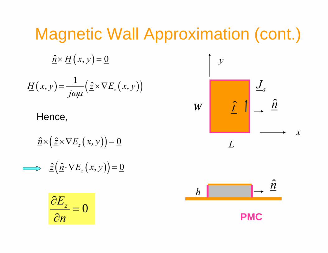
( ) ( )( )1 ˆ, ,zH x y z E x yjωμ
= ×∇
( )ˆ , 0n H x y× =
( )( )ˆ ˆ , 0zn z E x y× ×∇ =
( )( )ˆˆ , 0zz n E x y⋅∇ =
Magnetic Wall Approximation (cont.)
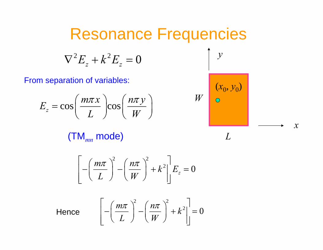
Resonance Frequencies2 2 0z zE k E∇ + =
cos coszm x n yE
L Wπ π⎛ ⎞ ⎛ ⎞= ⎜ ⎟ ⎜ ⎟
⎝ ⎠ ⎝ ⎠
2 22 0z
m n k EL Wπ π⎡ ⎤⎛ ⎞ ⎛ ⎞− − + =⎢ ⎥⎜ ⎟ ⎜ ⎟
⎝ ⎠ ⎝ ⎠⎢ ⎥⎣ ⎦
Hence2 2
2 0m n kL Wπ π⎡ ⎤⎛ ⎞ ⎛ ⎞− − + =⎢ ⎥⎜ ⎟ ⎜ ⎟
⎝ ⎠ ⎝ ⎠⎢ ⎥⎣ ⎦
x
y
L
W(x0, y0)
From separation of variables:
(TMmn mode)
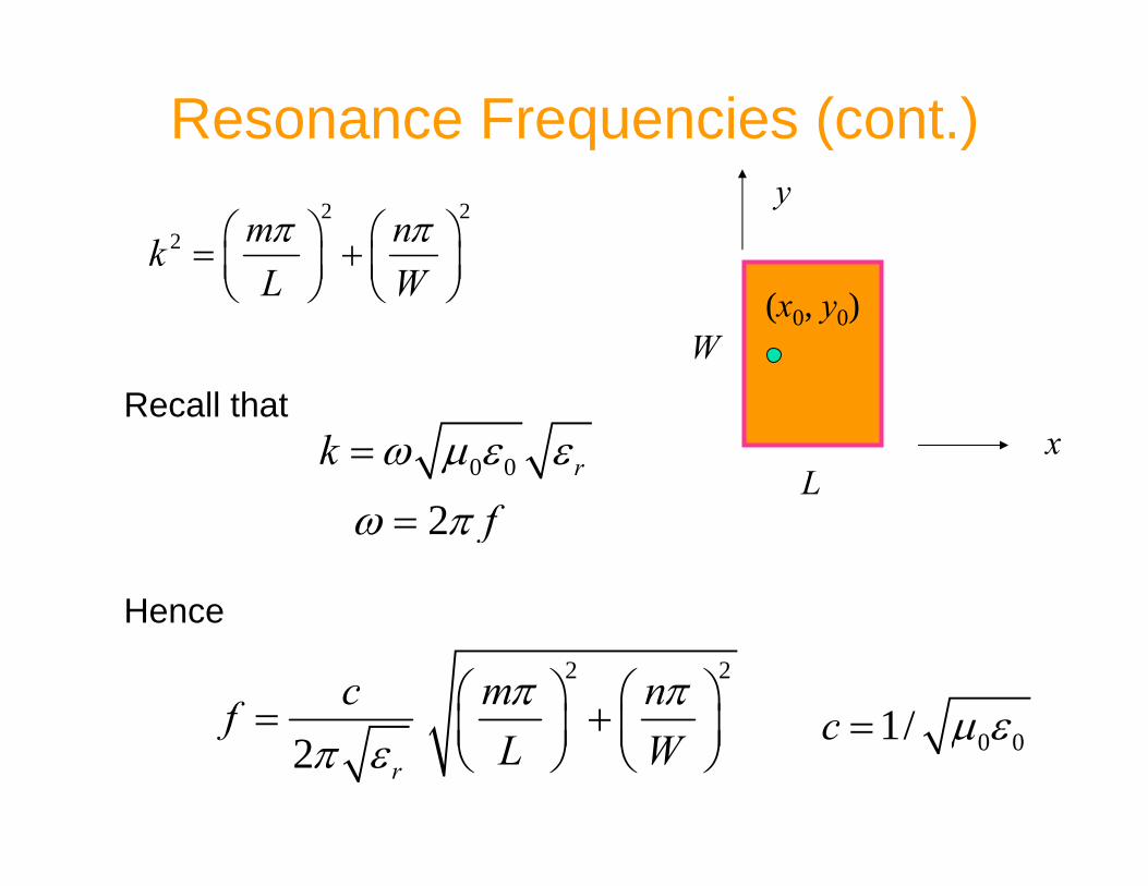
Resonance Frequencies (cont.)2 2
2 m nkL Wπ π⎛ ⎞ ⎛ ⎞= +⎜ ⎟ ⎜ ⎟
⎝ ⎠ ⎝ ⎠
0 0 rk ω μ ε ε=Recall that
2 fω π=
Hence2 2
2 r
c m nfL Wπ π
π ε⎛ ⎞ ⎛ ⎞= +⎜ ⎟ ⎜ ⎟⎝ ⎠ ⎝ ⎠ 0 01/c μ ε=
x
y
L
W(x0, y0)
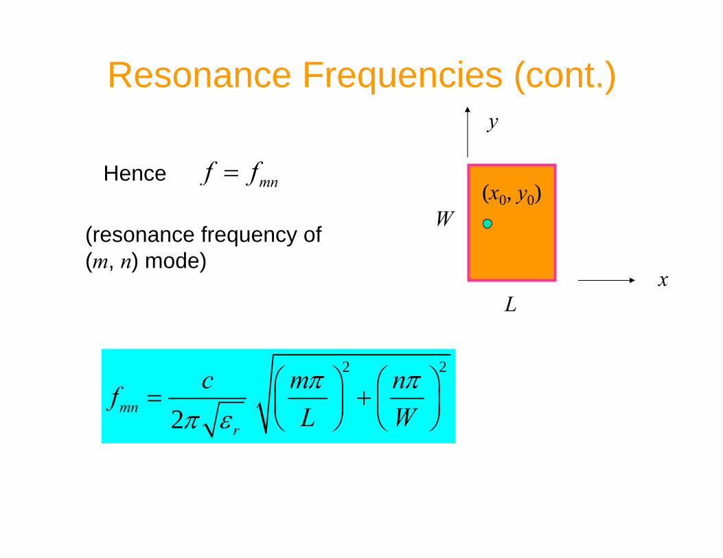
2 2
2mnr
c m nfL Wπ π
π ε⎛ ⎞ ⎛ ⎞= +⎜ ⎟ ⎜ ⎟⎝ ⎠ ⎝ ⎠
Hence mnf f=
(resonance frequency of (m, n) mode)
Resonance Frequencies (cont.)
x
y
L
W(x0, y0)
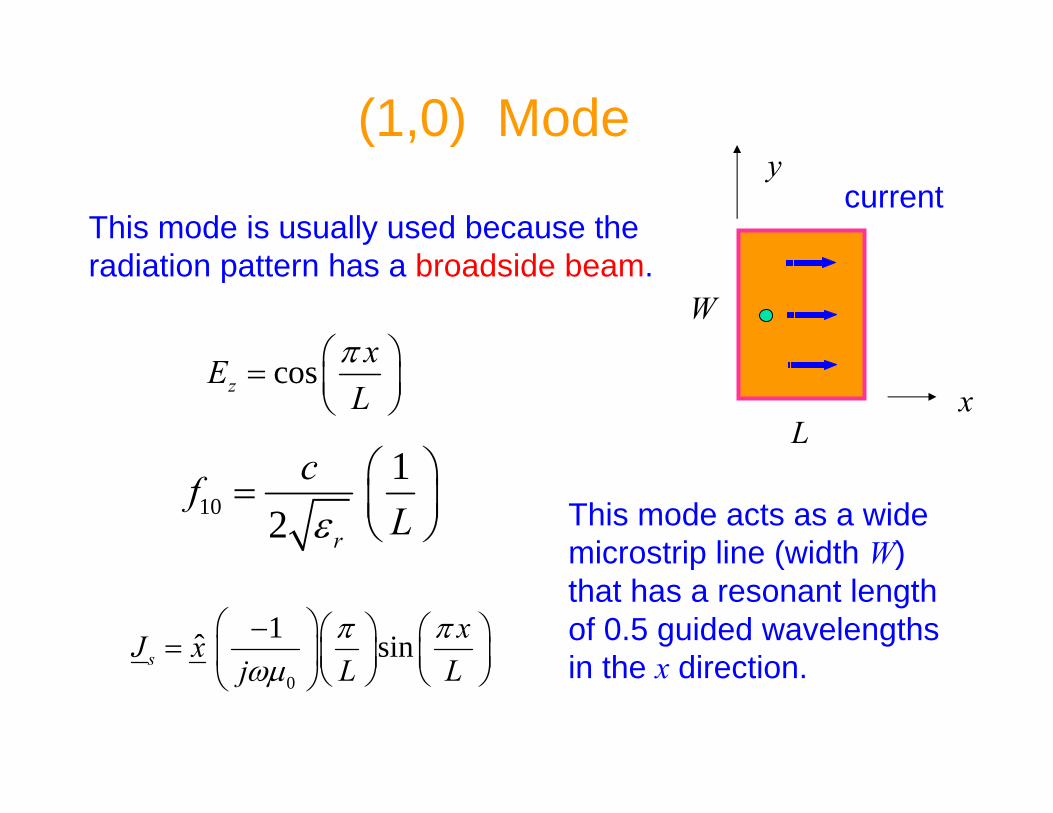
(1,0) Mode
This mode is usually used because the radiation pattern has a broadside beam.
101
2 r
cfLε
⎛ ⎞= ⎜ ⎟⎝ ⎠
coszxE
Lπ⎛ ⎞= ⎜ ⎟
⎝ ⎠
0
1ˆ sinsxJ x
j L Lπ π
ωμ⎛ ⎞− ⎛ ⎞ ⎛ ⎞= ⎜ ⎟⎜ ⎟ ⎜ ⎟
⎝ ⎠ ⎝ ⎠⎝ ⎠
This mode acts as a wide microstrip line (width W) that has a resonant length of 0.5 guided wavelengths in the x direction.
x
y
L
W
current
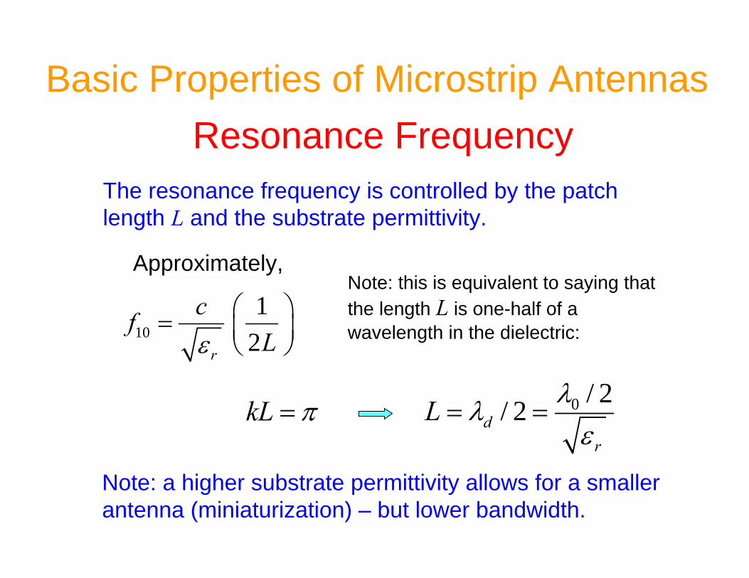
Basic Properties of Microstrip Antennas
The resonance frequency is controlled by the patch length L and the substrate permittivity.
Resonance Frequency
101
2r
cfLε
⎛ ⎞= ⎜ ⎟⎝ ⎠
Note: a higher substrate permittivity allows for a smaller antenna (miniaturization) – but lower bandwidth.
Approximately,Note: this is equivalent to saying that the length L is one-half of a wavelength in the dielectric:
0 / 2/ 2dr
L λλε
= =kL π=
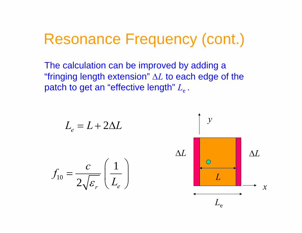
The calculation can be improved by adding a “fringing length extension” ΔL to each edge of the patch to get an “effective length” Le .
Resonance Frequency (cont.)
101
2 er
cfLε
⎛ ⎞= ⎜ ⎟
⎝ ⎠
2eL L L= + Δy
xL
Le
ΔLΔL
Resonance Frequency (cont.)
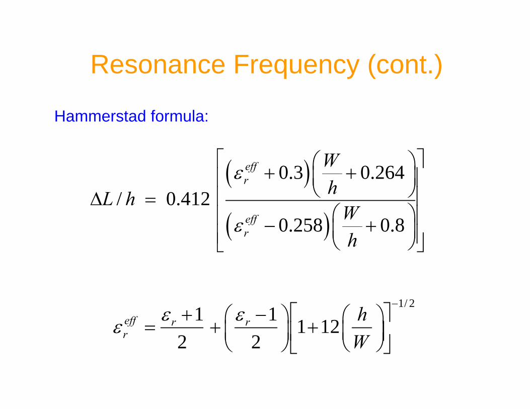
Hammerstad formula:
( )
( )
0.3 0.264/ 0.412
0.258 0.8
effr
effr
WhL h
Wh
ε
ε
⎡ ⎤⎛ ⎞+ +⎜ ⎟⎢ ⎥⎝ ⎠⎢ ⎥Δ =⎛ ⎞⎢ ⎥− +⎜ ⎟⎢ ⎥⎝ ⎠⎣ ⎦
1/ 21 1 1 12
2 2eff r rr
hW
ε εε−
⎡ ⎤+ −⎛ ⎞ ⎛ ⎞= + + ⎜ ⎟⎜ ⎟ ⎢ ⎥⎝ ⎠⎝ ⎠ ⎣ ⎦
Resonance Frequency (cont.)
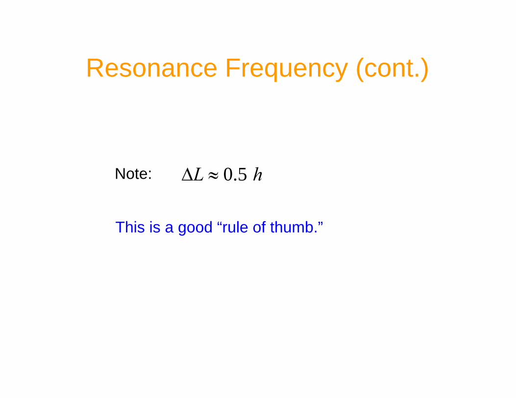
Note: 0.5L hΔ ≈
This is a good “rule of thumb.”
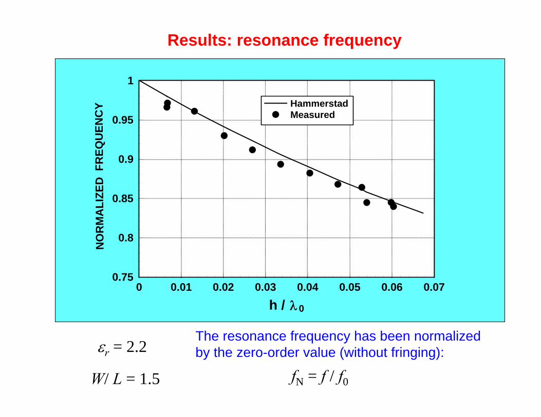
0 0.01 0.02 0.03 0.04 0.05 0.06 0.07h / λ0
0.75
0.8
0.85
0.9
0.95
1
NO
RM
ALI
ZED
FR
EQU
ENC
Y HammerstadMeasured
W/ L = 1.5
εr = 2.2The resonance frequency has been normalized by the zero-order value (without fringing):
fN = f / f0
Results: resonance frequency
Basic Properties of Microstrip Antennas
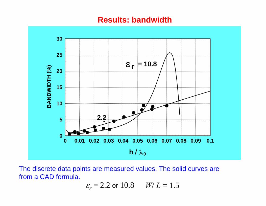
• The bandwidth is directly proportional to substrate thickness h.
• However, if h is greater than about 0.05 λ0 , the probe inductance becomes large enough so that matching is difficult.
• The bandwidth is inversely proportional to εr (a foam substrate gives a high bandwidth).
Bandwidth: substrate effects
Basic Properties of Microstrip Antennas
• The bandwidth is directly proportional to the width W.
Bandwidth: patch geometry
Normally W < 2L because of geometry constraints:
W = 1.5 L is typical.
Basic Properties of Microstrip Antennas
Bandwidth: typical results
• For a typical substrate thickness (h / λ0 = 0.02), and a typical substrate permittivity (εr = 2.2) the bandwidth is about 3%.
• By using a thick foam substrate, bandwidth of about 10% can be achieved.
• By using special feeding techniques (aperture coupling) and stacked patches, bandwidth of over 50% have been achieved.
0 0.01 0.02 0.03 0.04 0.05 0.06 0.07 0.08 0.09 0.1
h / λ0
0
5
10
15
20
25
30
BA
ND
WID
TH (%
) ε r
2.2
= 10.8
W/ L = 1.5 εr = 2.2 or 10.8
Results: bandwidth
The discrete data points are measured values. The solid curves are from a CAD formula.
Basic Properties of Microstrip Antennas
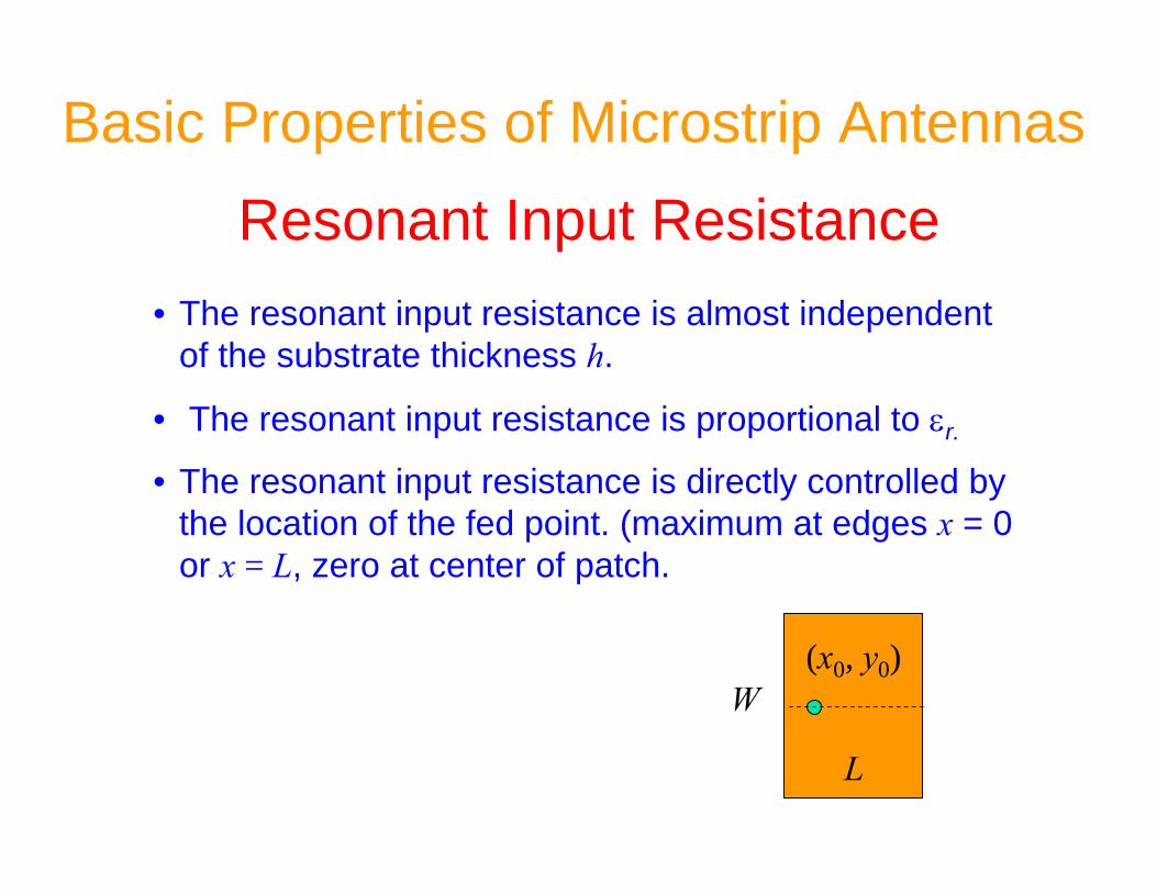
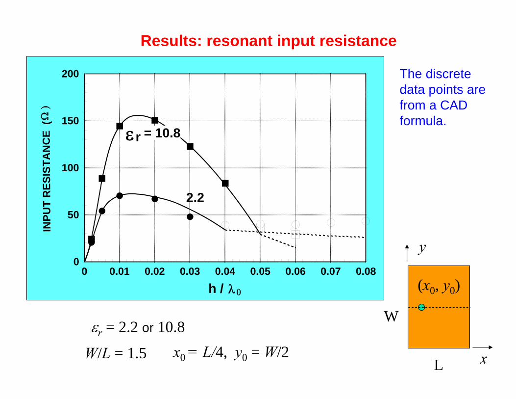
• The resonant input resistance is almost independent of the substrate thickness h.
• The resonant input resistance is proportional to εr.
• The resonant input resistance is directly controlled by the location of the fed point. (maximum at edges x = 0 or x = L, zero at center of patch.
Resonant Input Resistance
L
W(x0, y0)
L
Resonant Input Resistance (cont.)
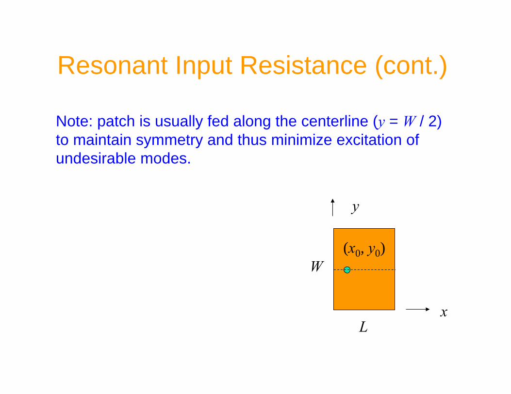
Note: patch is usually fed along the centerline (y = W / 2) to maintain symmetry and thus minimize excitation of undesirable modes.
Lx
W(x0, y0)
y
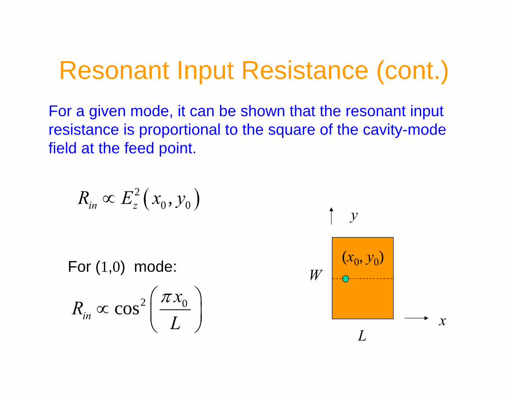
Resonant Input Resistance (cont.)For a given mode, it can be shown that the resonant input resistance is proportional to the square of the cavity-mode field at the feed point.
( )20 0,in zR E x y∝
For (1,0) mode:
2 0cosinxRL
π⎛ ⎞∝ ⎜ ⎟⎝ ⎠ L
x
W(x0, y0)
y
Resonant Input Resistance (cont.)
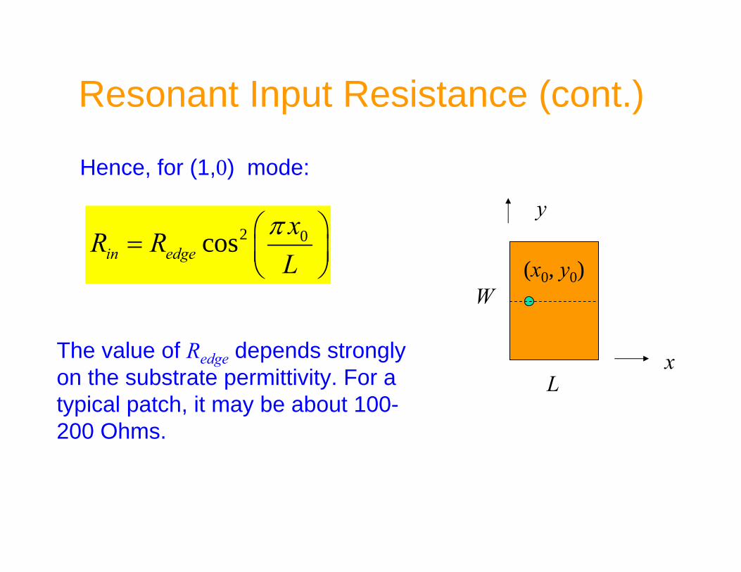
Hence, for (1,0) mode:
2 0cosin edgexR RL
π⎛ ⎞= ⎜ ⎟⎝ ⎠
The value of Redge depends strongly on the substrate permittivity. For a typical patch, it may be about 100-200 Ohms.
Lx
W(x0, y0)
y
0 0.01 0.02 0.03 0.04 0.05 0.06 0.07 0.08h / λ0
0
50
100
150
200
INPU
T R
ESIS
TAN
CE
( Ω
)
2.2
r = 10.8ε
εr = 2.2 or 10.8
W/L = 1.5 x0 = L/4, y0 = W/2
Results: resonant input resistance
The discrete data points are from a CAD formula.
L x
W
(x0, y0)
y
Basic Properties of Microstrip Antennas
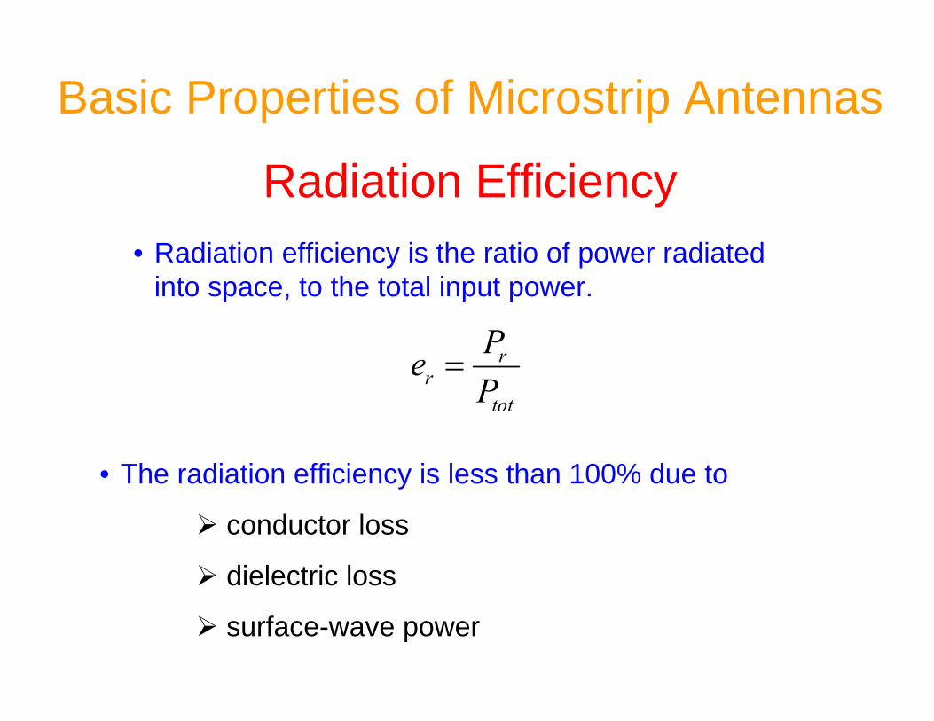
Radiation Efficiency
• The radiation efficiency is less than 100% due to
conductor loss
dielectric loss
surface-wave power
• Radiation efficiency is the ratio of power radiated into space, to the total input power.
rr
tot
PeP
=
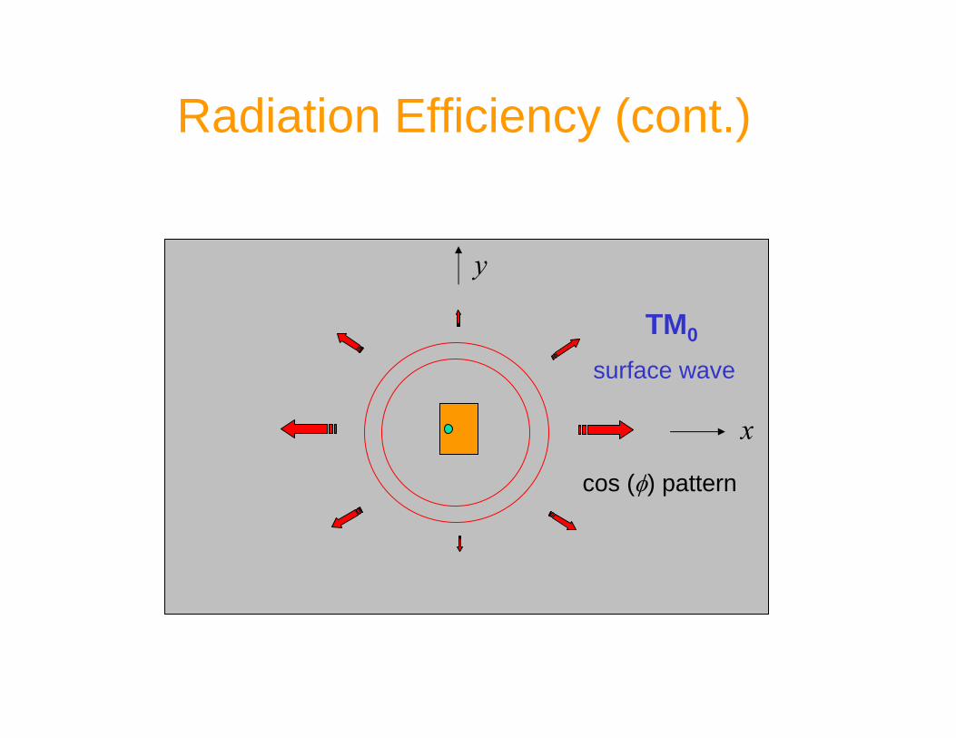
Radiation Efficiency (cont.)
surface wave
TM0
cos (φ) pattern
x
y
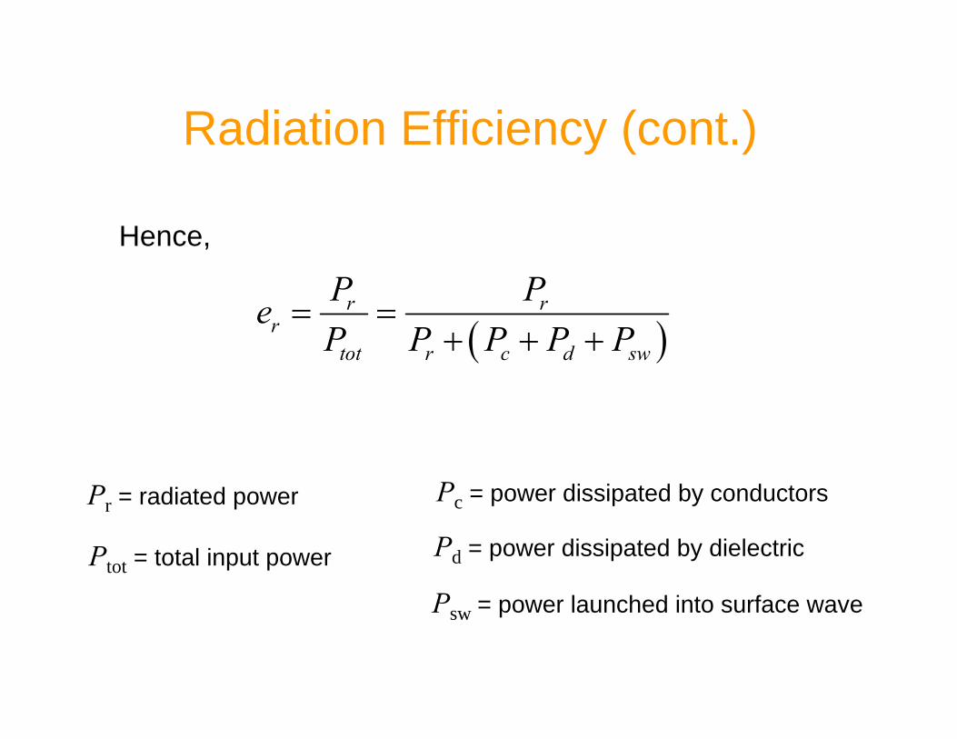
Radiation Efficiency (cont.)
( )r r
rtot r c d sw
P PeP P P P P
= =+ + +
Pr = radiated power
Ptot = total input power
Pc = power dissipated by conductors
Pd = power dissipated by dielectric
Psw = power launched into surface wave
Hence,
Radiation Efficiency (cont.)
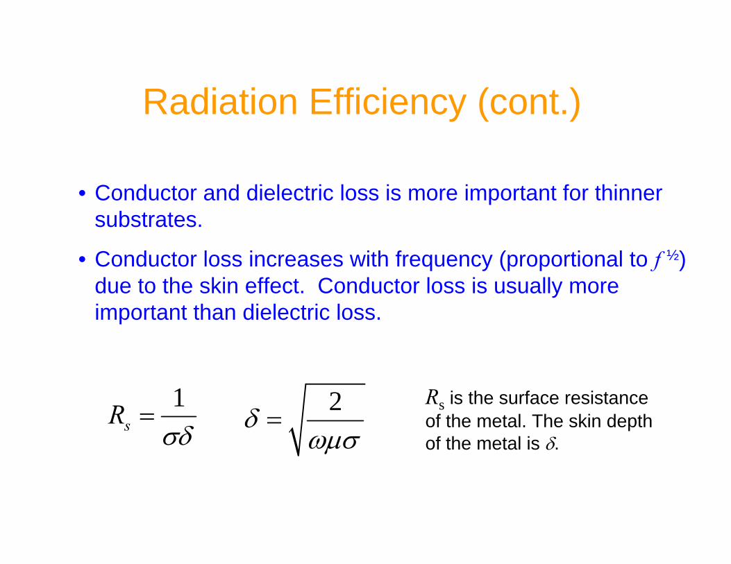
• Conductor and dielectric loss is more important for thinner substrates.
• Conductor loss increases with frequency (proportional to f ½) due to the skin effect. Conductor loss is usually more important than dielectric loss.
2δωμσ
=1
sRσδ
=Rs is the surface resistance of the metal. The skin depth of the metal is δ.
Radiation Efficiency (cont.)
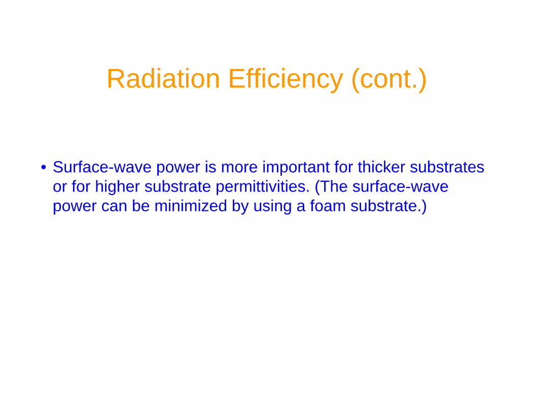
• Surface-wave power is more important for thicker substrates or for higher substrate permittivities. (The surface-wave power can be minimized by using a foam substrate.)
Radiation Efficiency (cont.)
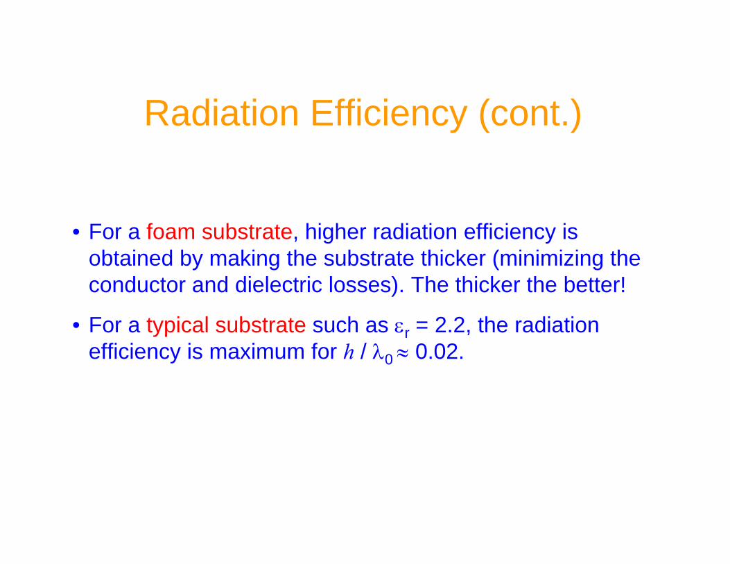
• For a foam substrate, higher radiation efficiency is obtained by making the substrate thicker (minimizing the conductor and dielectric losses). The thicker the better!
• For a typical substrate such as εr = 2.2, the radiation efficiency is maximum for h / λ0 ≈ 0.02.
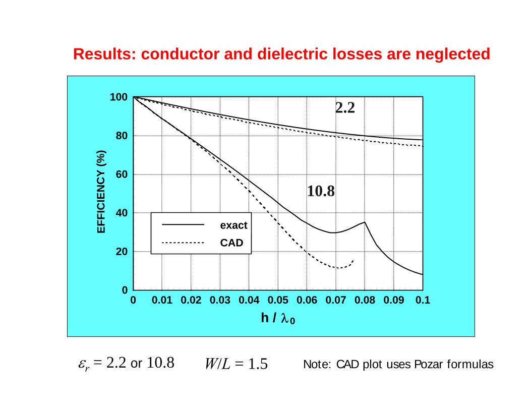
εr = 2.2 or 10.8 W/L = 1.5
0 0.01 0.02 0.03 0.04 0.05 0.06 0.07 0.08 0.09 0.1h / λ0
0
20
40
60
80
100EF
FIC
IEN
CY
(%)
exactCAD
Results: conductor and dielectric losses are neglected
2.2
10.8
Note: CAD plot uses Pozar formulas
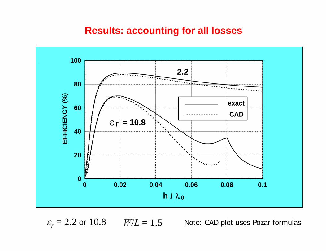
0 0.02 0.04 0.06 0.08 0.1h / λ0
0
20
40
60
80
100EF
FIC
IEN
CY
(%)
ε = 10.8
2.2
exactCAD
r
εr = 2.2 or 10.8 W/L = 1.5
Results: accounting for all losses
Note: CAD plot uses Pozar formulas
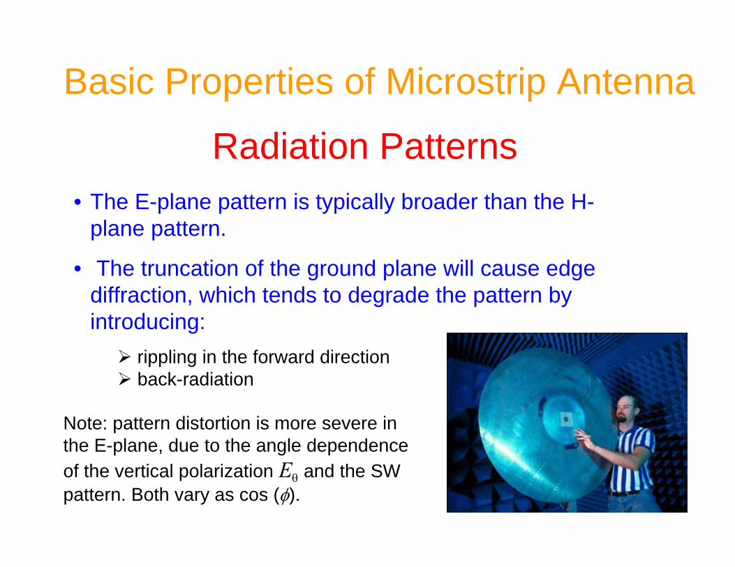
Basic Properties of Microstrip Antenna
Radiation Patterns• The E-plane pattern is typically broader than the H-
plane pattern.
• The truncation of the ground plane will cause edge diffraction, which tends to degrade the pattern by introducing:
rippling in the forward directionback-radiation
Note: pattern distortion is more severe in the E-plane, due to the angle dependence of the vertical polarization Eθ and the SW pattern. Both vary as cos (φ).
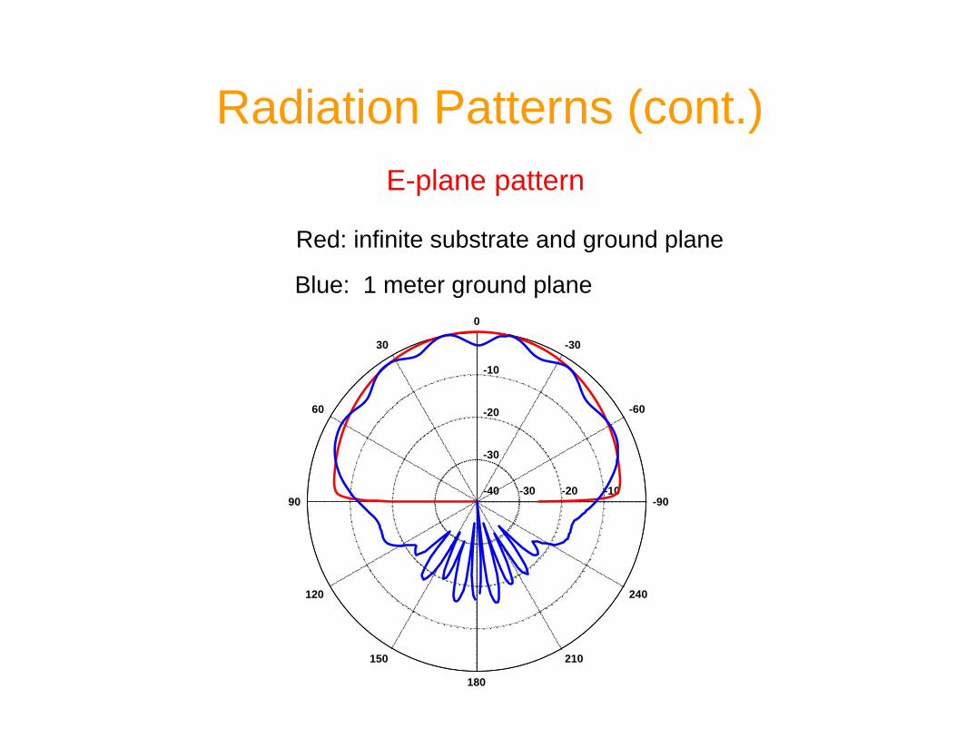
Radiation Patterns (cont.)
-90
-60
-30
0
30
60
90
120
150
180
210
240
-40
-30
-30
-20
-20
-10
-10
E-plane pattern
Red: infinite substrate and ground plane
Blue: 1 meter ground plane
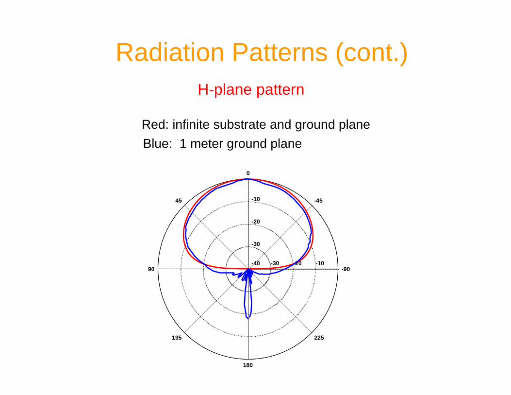
H-plane pattern
Red: infinite substrate and ground planeBlue: 1 meter ground plane
-90
-45
0
45
90
135
180
225
-40
-30
-30
-20
-20
-10
-10
Radiation Patterns (cont.)
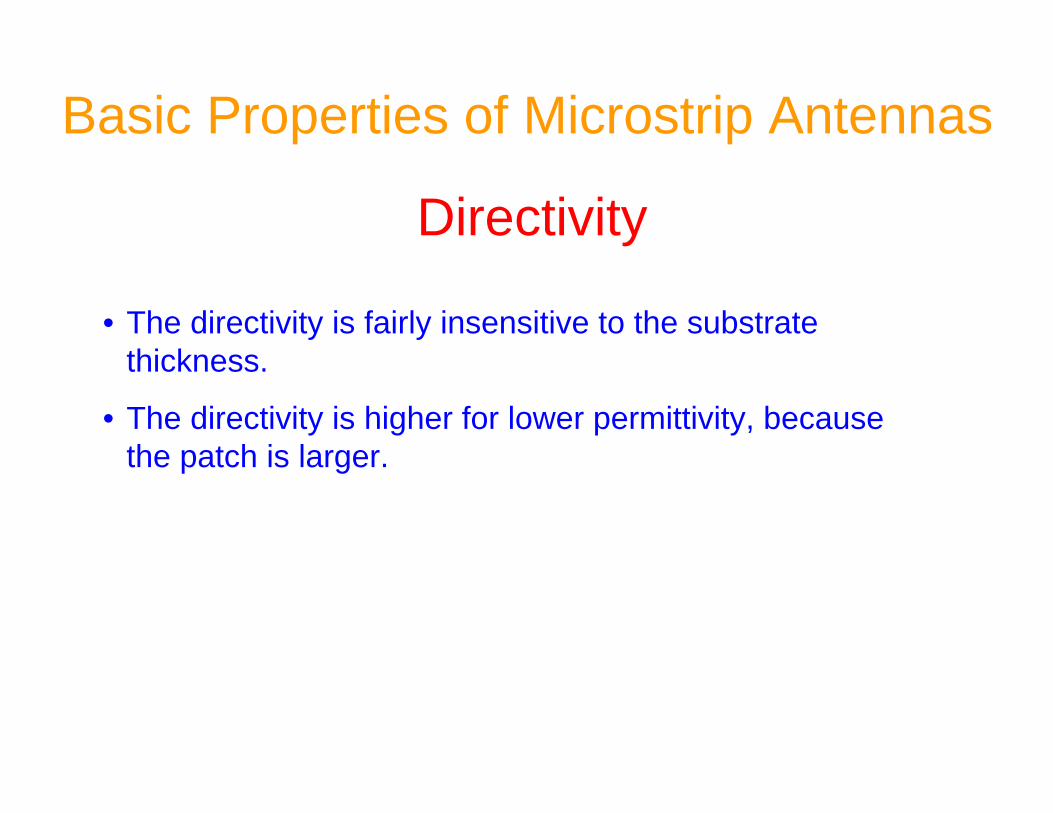
Basic Properties of Microstrip Antennas
Directivity
• The directivity is fairly insensitive to the substrate thickness.
• The directivity is higher for lower permittivity, because the patch is larger.
0 0.01 0.02 0.03 0.04 0.05 0.06 0.07 0.08 0.09 0.1h / λ0
0
2
4
6
8
10D
IREC
TIVI
TY (
dB)
exact
CAD
= 2.2
10.8
ε r
εr = 2.2 or 10.8 W/ L = 1.5
Results: Directivity
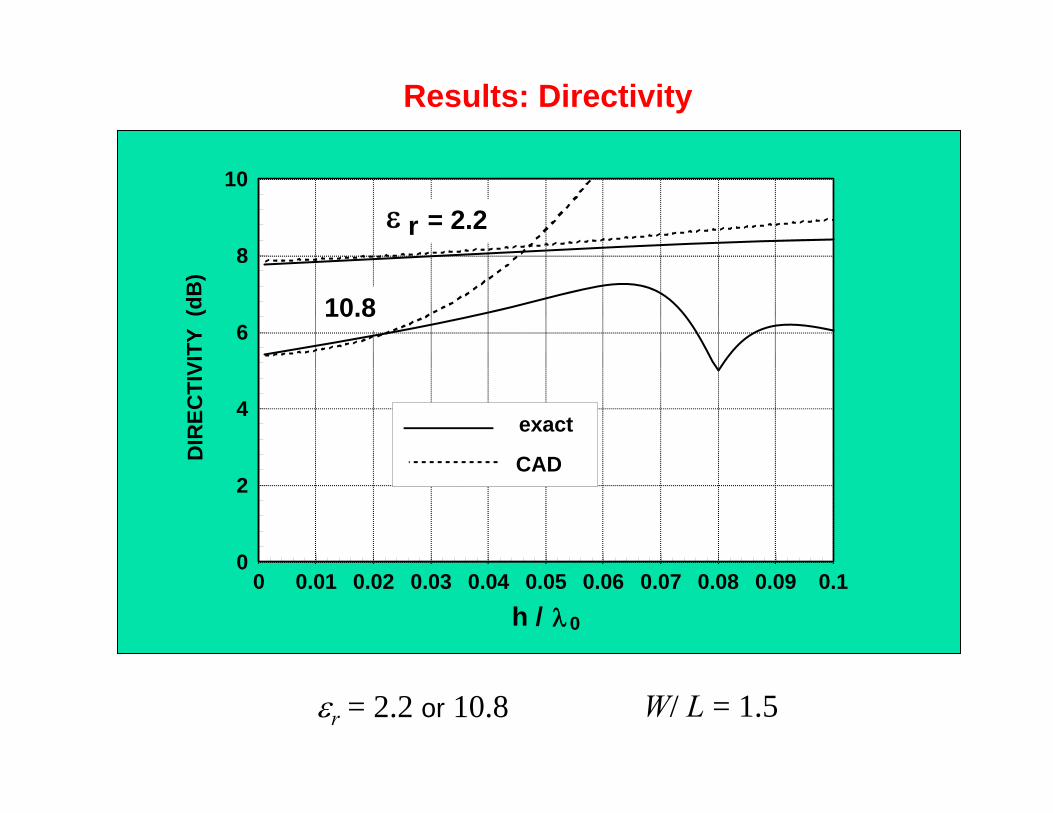
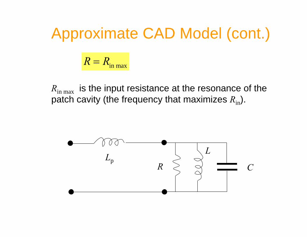
Approximate CAD Model for Zin
• Near the resonance frequency, the patch cavity can be approximately modeled as an RLC circuit.
• A probe inductance Lp is added in series, to account for the “probe inductance”.
LpR C
L
Zin
probe patch cavity
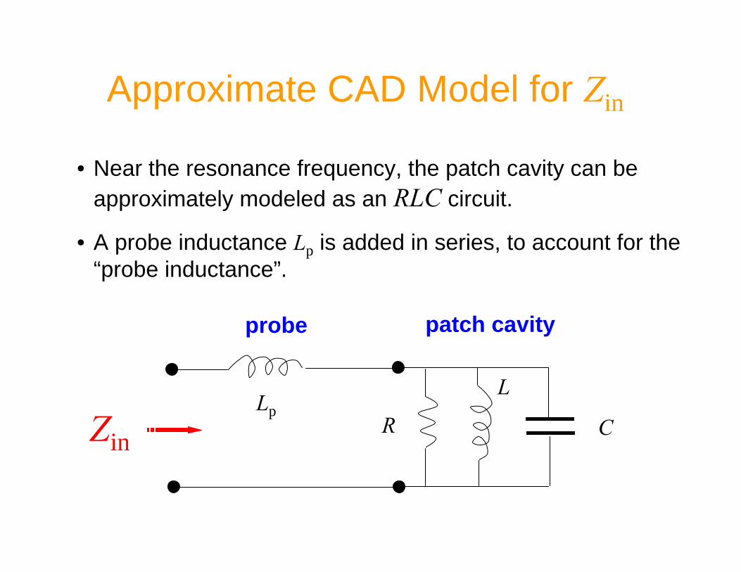
Approximate CAD Model (cont.)
LpR C
L
( )01 2 / 1in pRZ j L
j Q f fω≈ +
+ −
0
RQLω
=12
BWQ
= BW is defined here by SWR < 2.0.
0 012 fLC
ω π= =
Approximate CAD Model (cont.)
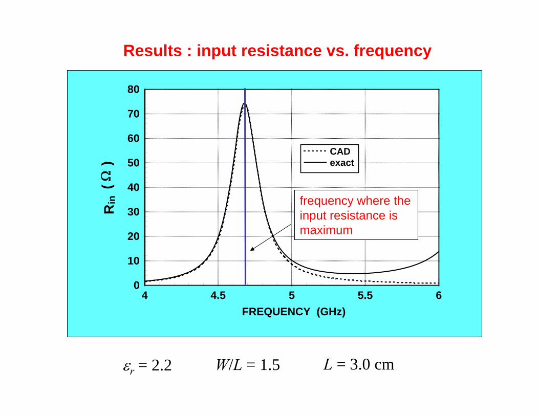
in maxR R=
Rin max is the input resistance at the resonance of the patch cavity (the frequency that maximizes Rin).
LpR C
L
4 4.5 5 5.5 6FREQUENCY (GHz)
0
10
20
30
40
50
60
70
80
Rin
( Ω
)
CADexact
Results : input resistance vs. frequency
εr = 2.2 W/L = 1.5 L = 3.0 cm
frequency where the input resistance is maximum
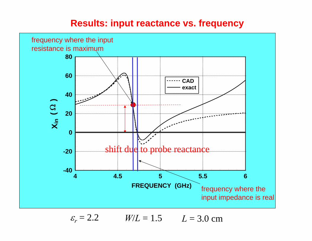
Results: input reactance vs. frequency
εr = 2.2 W/L = 1.5
4 4.5 5 5.5 6FREQUENCY (GHz)
-40
-20
0
20
40
60
80X i
n ( Ω
)
CADexact
L = 3.0 cm
frequency where the input resistance is maximum
frequency where the input impedance is real
shift due to probe reactance
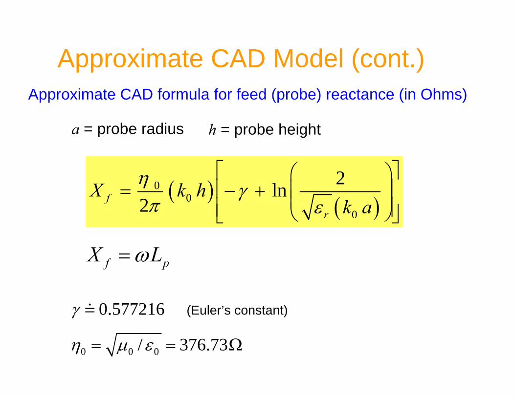
Approximate CAD Model (cont.)
0.577216γ
( )( )
00
0
2ln2f
r
X k hk a
η γπ ε
⎡ ⎤⎛ ⎞= ⎢− + ⎥⎜ ⎟⎜ ⎟⎢ ⎥⎝ ⎠⎣ ⎦
(Euler’s constant)
Approximate CAD formula for feed (probe) reactance (in Ohms)
f pX Lω=
0 0 0/ 376.73η μ ε= = Ω
a = probe radius h = probe height
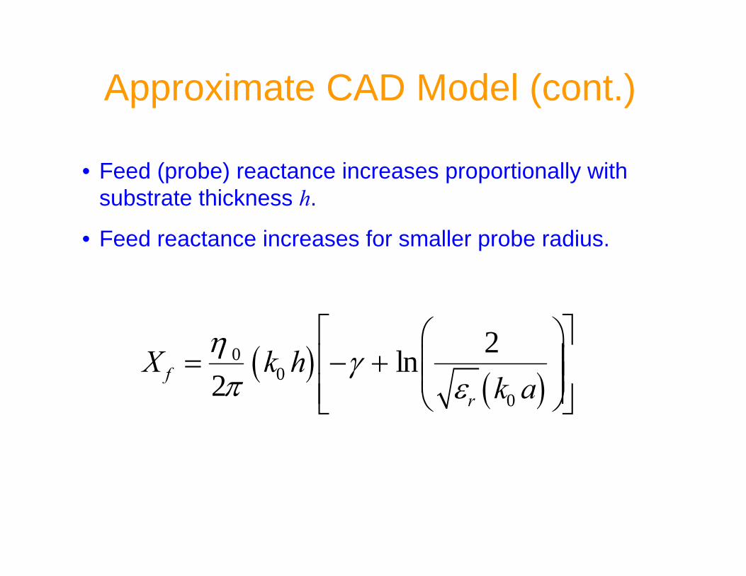
Approximate CAD Model (cont.)
( )( )
00
0
2ln2f
r
X k hk a
η γπ ε
⎡ ⎤⎛ ⎞= ⎢− + ⎥⎜ ⎟⎜ ⎟⎢ ⎥⎝ ⎠⎣ ⎦
• Feed (probe) reactance increases proportionally with substrate thickness h.
• Feed reactance increases for smaller probe radius.
0 0.1 0.2 0.3 0.4 0.5 0.6 0.7 0.8 0.9 1Xr
0
5
10
15
20
25
30
35
40
X f (
Ω)
CADexact
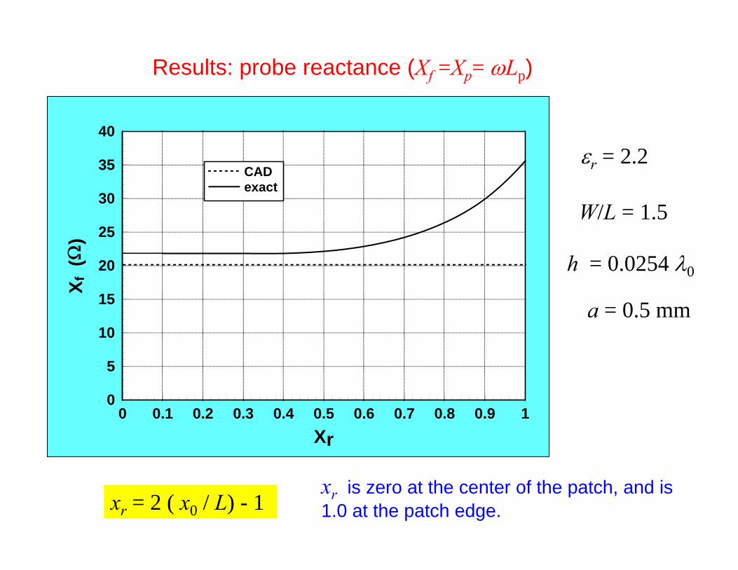
Results: probe reactance (Xf =Xp= ωLp)
xr = 2 ( x0 / L) - 1 xr is zero at the center of the patch, and is 1.0 at the patch edge.
εr = 2.2
W/L = 1.5
h = 0.0254 λ0
a = 0.5 mm
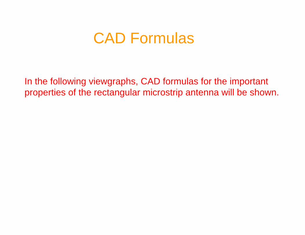
CAD Formulas
In the following viewgraphs, CAD formulas for the important properties of the rectangular microstrip antenna will be shown.
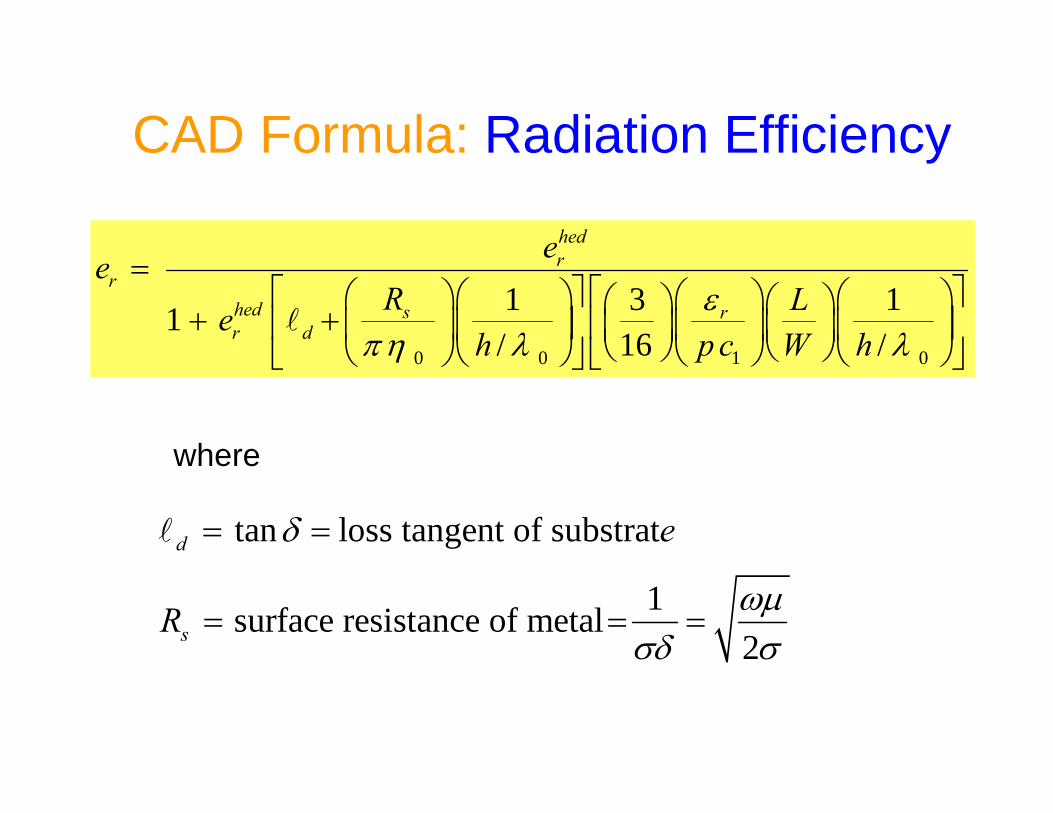
CAD Formula: Radiation Efficiency
0 0 1 0
1 3 11/ 16 /
hedr
rhed s rr d
eeR Le
h p c W hε
π η λ λ
=⎡ ⎤ ⎡ ⎤⎛ ⎞⎛ ⎞ ⎛ ⎞⎛ ⎞⎛ ⎞ ⎛ ⎞+ +⎢ ⎥ ⎢ ⎥⎜ ⎟⎜ ⎟ ⎜ ⎟⎜ ⎟⎜ ⎟ ⎜ ⎟
⎝ ⎠ ⎝ ⎠⎝ ⎠⎝ ⎠⎝ ⎠ ⎝ ⎠⎣ ⎦ ⎣ ⎦
where
tan loss tangent of substratd eδ= =
1surface resistance of metal2sR ωμ
σδ σ= = =
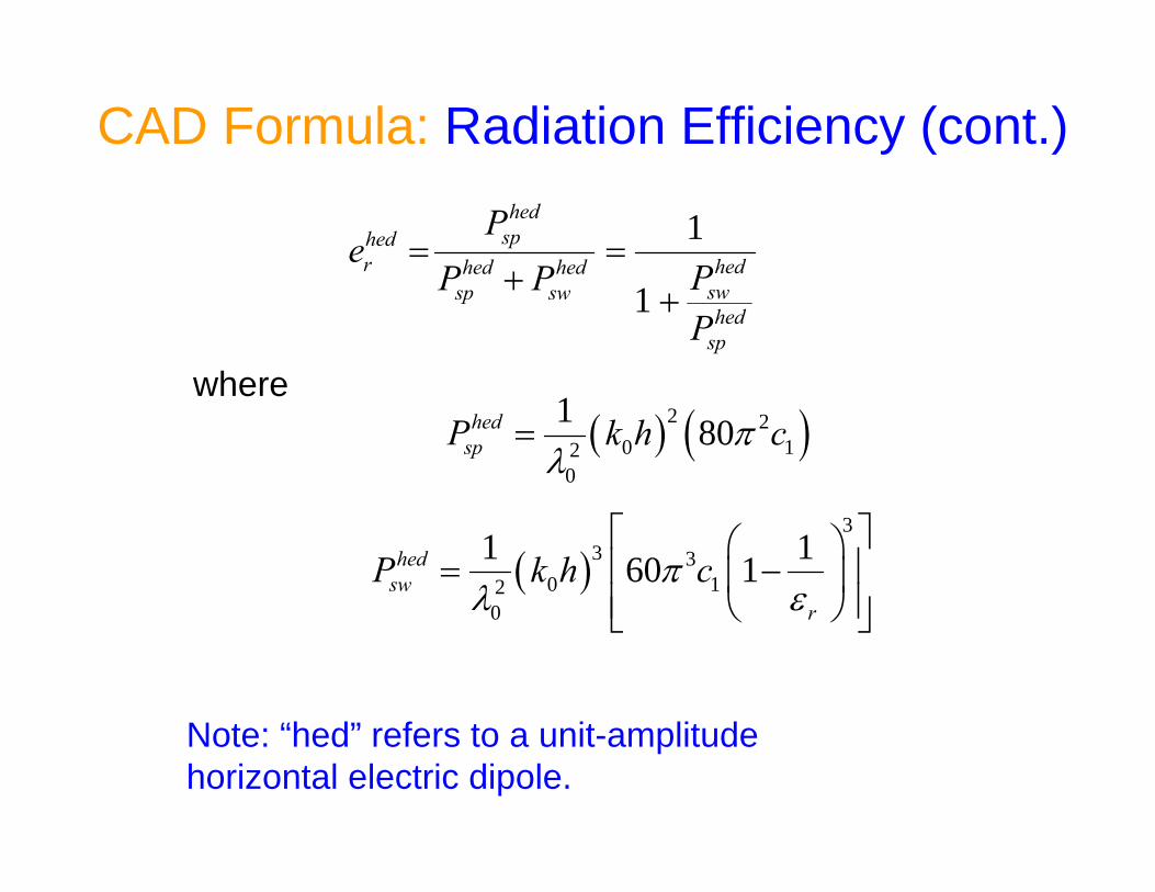
CAD Formula: Radiation Efficiency (cont.)
where
Note: “hed” refers to a unit-amplitude horizontal electric dipole.
( ) ( )2 20 12
0
1 80hedspP k h cπ
λ=
1
1
hedsphed
r hedhed hedswsp swhed
sp
Pe
PP PP
= =+ +
( )3
3 30 12
0
1 160 1hedsw
r
P k h cπλ ε
⎡ ⎤⎛ ⎞⎢ ⎥= −⎜ ⎟⎢ ⎥⎝ ⎠⎣ ⎦
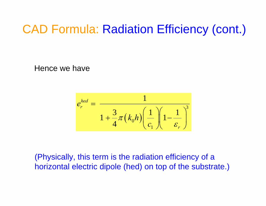
CAD Formula: Radiation Efficiency (cont.)
( )3
01
1
3 1 11 14
hedr
r
e
k hc
πε
=⎛ ⎞⎛ ⎞
+ −⎜ ⎟⎜ ⎟⎝ ⎠⎝ ⎠
Hence we have
(Physically, this term is the radiation efficiency of a horizontal electric dipole (hed) on top of the substrate.)
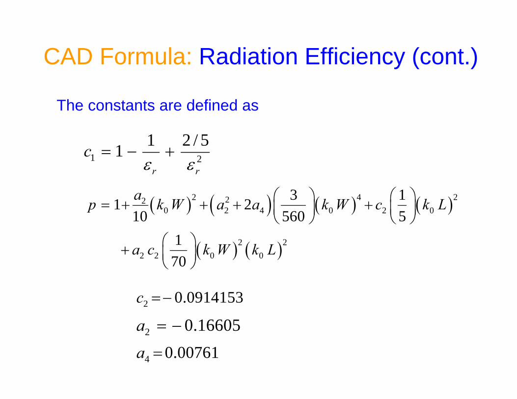
1 2
1 2 / 51r r
cε ε
= − +
( ) ( ) ( ) ( )
( ) ( )
2 4 2220 2 4 0 2 0
2 22 2 0 0
3 11 210 560 5
170
ap k W a a k W c k L
a c k W k L
⎛ ⎞ ⎛ ⎞= + + + +⎜ ⎟ ⎜ ⎟⎝ ⎠ ⎝ ⎠
⎛ ⎞+ ⎜ ⎟⎝ ⎠
The constants are defined as
2 0.16605a = −
4 0.00761a =
2 0.0914153c = −
CAD Formula: Radiation Efficiency (cont.)
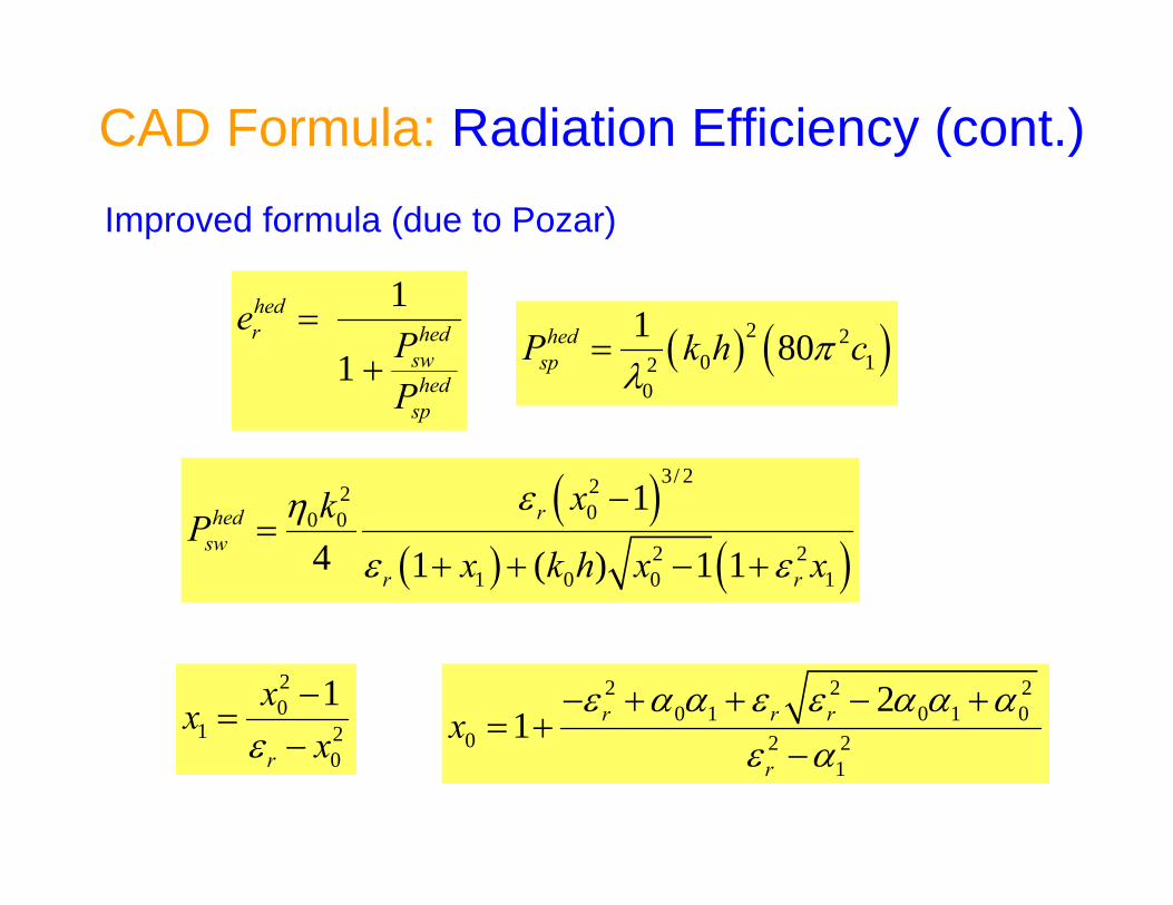
CAD Formula: Radiation Efficiency (cont.)
1
1
hedr hed
swhed
sp
ePP
=+
Improved formula (due to Pozar)
( )( ) ( )
3/ 22200 0
2 21 0 0 1
14 1 ( ) 1 1
rhedsw
r r
xkPx k h x x
εη
ε ε
−=
+ + − +
20
1 20
1
r
xxxε
−=
−
2 2 20 1 0 1 0
0 2 21
21 r r r
r
xε α α ε ε α α α
ε α− + + − +
= +−
( ) ( )2 20 12
0
1 80hedspP k h cπ
λ=
CAD Formula: Radiation Efficiency (cont.)
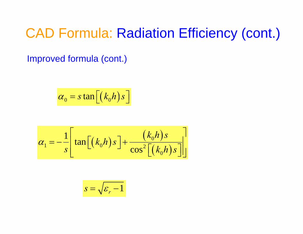
Improved formula (cont.)
( )0 0tans k h sα ⎡ ⎤= ⎣ ⎦
( ) ( )( )0
1 0 20
1 tancos
k h sk h s
s k h sα
⎡ ⎤⎡ ⎤= − +⎢ ⎥⎣ ⎦ ⎡ ⎤⎢ ⎥⎣ ⎦⎣ ⎦
1rs ε= −
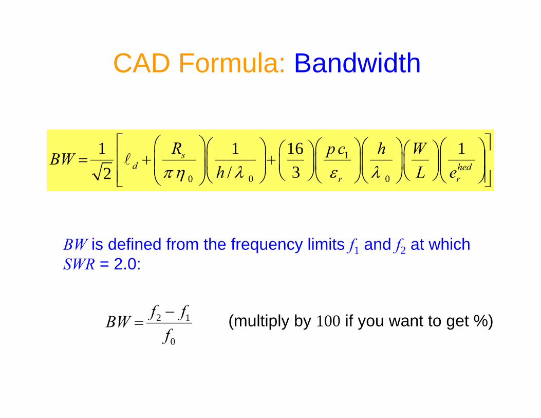
CAD Formula: Bandwidth
1
0 0 0
1 1 16 1/ 32
sd hed
r r
R p c h WBWh L eπ η λ ε λ
⎡ ⎤⎛ ⎞⎛ ⎞ ⎛ ⎞⎛ ⎞ ⎛ ⎞⎛ ⎞ ⎛ ⎞= + +⎢ ⎥⎜ ⎟⎜ ⎟ ⎜ ⎟⎜ ⎟ ⎜ ⎟⎜ ⎟ ⎜ ⎟⎜ ⎟ ⎝ ⎠ ⎝ ⎠⎢ ⎥⎝ ⎠ ⎝ ⎠⎝ ⎠ ⎝ ⎠⎝ ⎠⎣ ⎦
BW is defined from the frequency limits f1 and f2 at which SWR = 2.0:
2 1
0
f fBWf−
= (multiply by 100 if you want to get %)
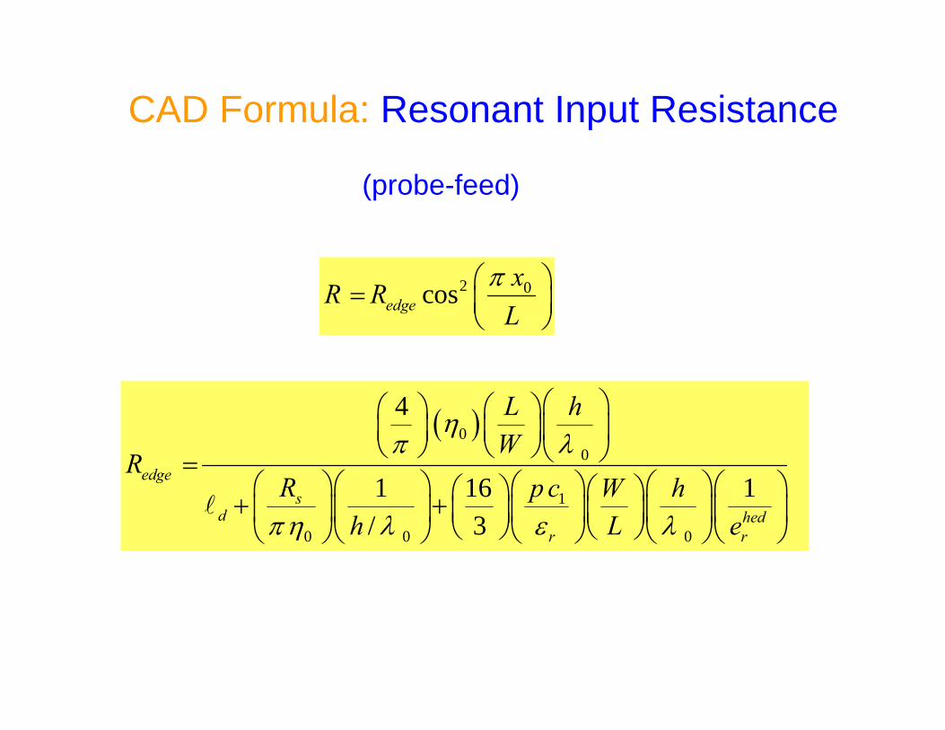
CAD Formula: Resonant Input Resistance
2 0cosedgexR R
Lπ⎛ ⎞= ⎜ ⎟
⎝ ⎠
(probe-feed)
( )00
1
0 0 0
4
1 16 1/ 3
edges
d hedr r
L hW
RR p c W h
h L e
ηπ λ
π η λ ε λ
⎛ ⎞⎛ ⎞ ⎛ ⎞⎜ ⎟⎜ ⎟ ⎜ ⎟
⎝ ⎠ ⎝ ⎠⎝ ⎠=⎛ ⎞⎛ ⎞ ⎛ ⎞⎛ ⎞ ⎛ ⎞⎛ ⎞ ⎛ ⎞+ +⎜ ⎟⎜ ⎟ ⎜ ⎟⎜ ⎟ ⎜ ⎟⎜ ⎟ ⎜ ⎟
⎝ ⎠ ⎝ ⎠⎝ ⎠ ⎝ ⎠⎝ ⎠⎝ ⎠ ⎝ ⎠
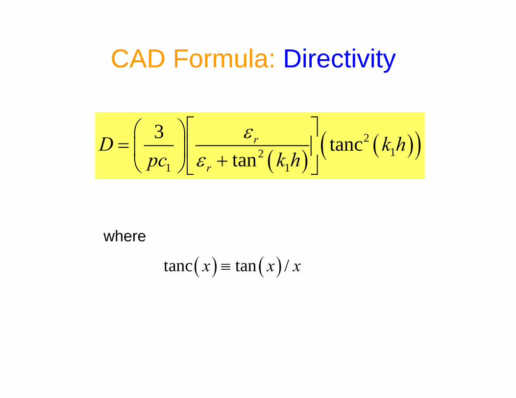
CAD Formula: Directivity
( ) ( )tanc tan /x x x≡
where
( ) ( )( )212
1 1
3 tanctan
r
r
D k hpc k h
εε
⎡ ⎤⎛ ⎞= ⎢ ⎥⎜ ⎟ +⎝ ⎠ ⎣ ⎦
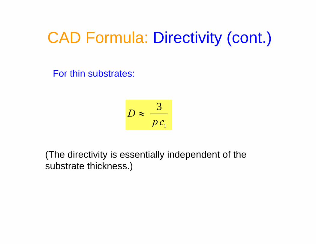
CAD Formula: Directivity (cont.)
1
3Dp c
≈
For thin substrates:
(The directivity is essentially independent of the substrate thickness.)
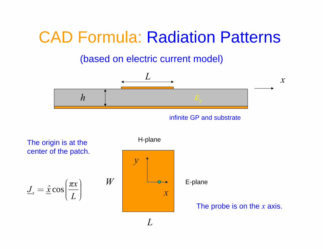
CAD Formula: Radiation Patterns(based on electric current model)
The origin is at the center of the patch.
L
rεh
infinite GP and substrate
x
The probe is on the x axis.
cossπxˆJ xL
⎛ ⎞⎟⎜= ⎟⎜ ⎟⎜⎝ ⎠
y
L
W E-plane
H-plane
x
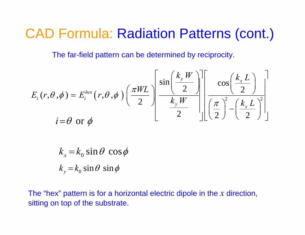
CAD Formula: Radiation Patterns (cont.)
( ) 22
sin cos2 2( , , ) , ,2
2 2 2
y x
hexi i
y x
k W k LWLE r E r k W k L
πθ φ θ φπ
⎡ ⎤ ⎡ ⎤⎛ ⎞ ⎛ ⎞⎢ ⎥ ⎢ ⎥⎜ ⎟ ⎜ ⎟⎛ ⎞ ⎝ ⎠ ⎝ ⎠⎢ ⎥ ⎢ ⎥= ⎜ ⎟ ⎢ ⎥ ⎢ ⎥⎝ ⎠ ⎛ ⎞⎛ ⎞ −⎢ ⎥ ⎢ ⎥⎜ ⎟ ⎜ ⎟
⎝ ⎠ ⎝ ⎠⎣ ⎦⎣ ⎦
0 sin cosxk k θ φ=
0 sin sinyk k θ φ=
The “hex” pattern is for a horizontal electric dipole in the x direction, sitting on top of the substrate.
ori θ φ=
The far-field pattern can be determined by reciprocity.
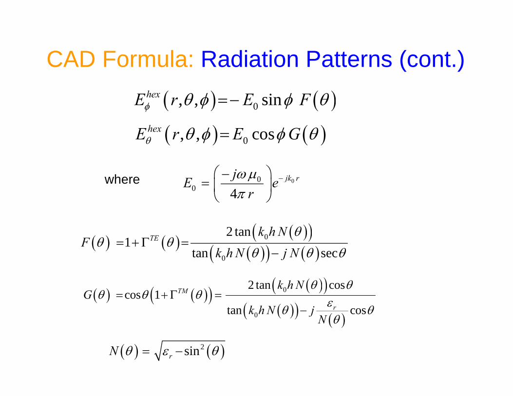
( ) ( )0, , coshexE r E Gθ θ φ φ θ=
( ) ( )0, , sinhexE r E Fφ θ φ φ θ= −
where
( ) ( ) ( )( )( )( ) ( )
0
0
2 tan1
tan secTE k h N
Fk h N j N
θθ θ
θ θ θ= + Γ =
−
( ) ( )( ) ( )( )( )( ) ( )
0
0
2 tan coscos 1
tan cos
TM
r
k h NG
k h N jN
θ θθ θ θ εθ θ
θ
= + Γ =−
( ) ( )2sinrN θ ε θ= −
000 4
jk rjE er
ω μπ
−⎛ ⎞−= ⎜ ⎟
⎝ ⎠
CAD Formula: Radiation Patterns (cont.)
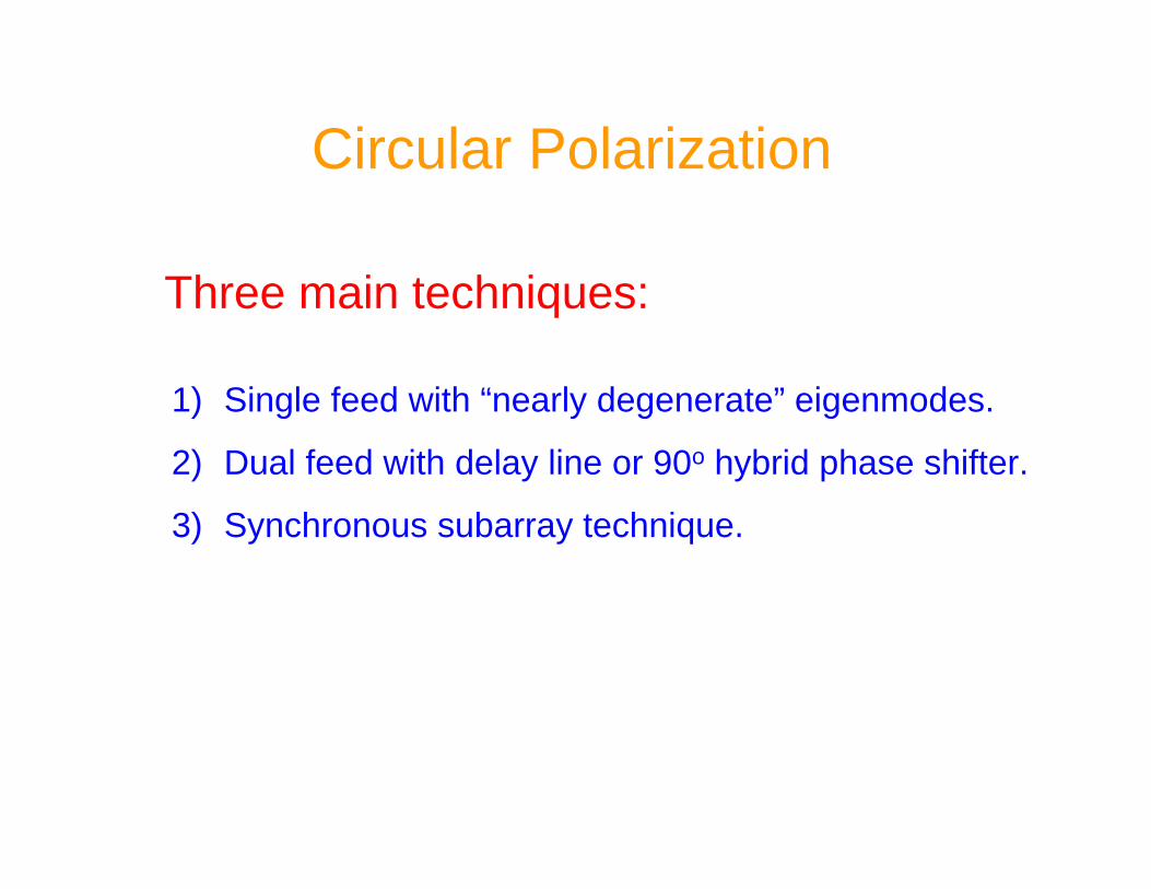
Circular Polarization
Three main techniques:
1) Single feed with “nearly degenerate” eigenmodes.
2) Dual feed with delay line or 90o hybrid phase shifter.
3) Synchronous subarray technique.
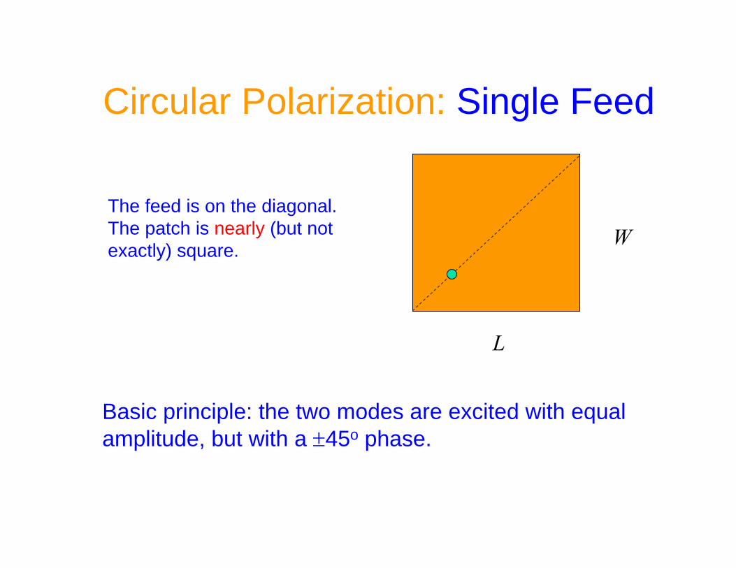
Circular Polarization: Single Feed
L
W
Basic principle: the two modes are excited with equal amplitude, but with a ±45o phase.
The feed is on the diagonal. The patch is nearly (but not exactly) square.
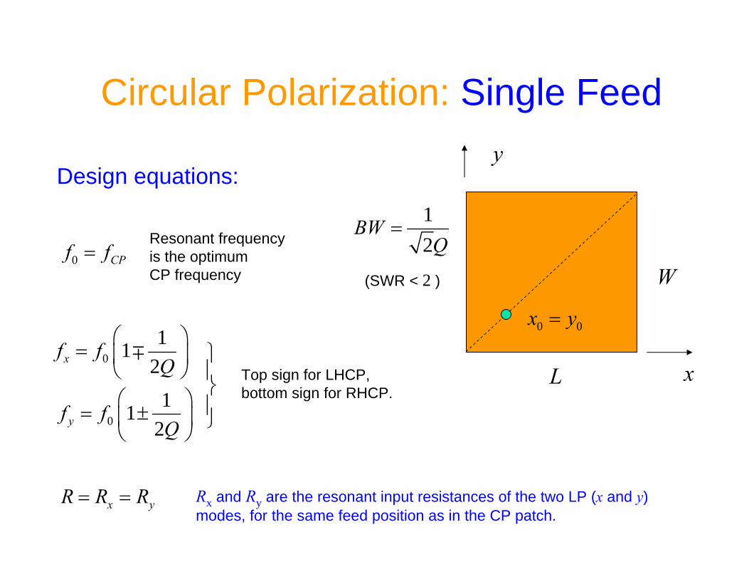
Circular Polarization: Single Feed
Design equations:
0 CPf f=
011
2xf fQ
⎛ ⎞= ⎜ ⎟
⎝ ⎠∓
011
2yf fQ
⎛ ⎞= ±⎜ ⎟
⎝ ⎠
Top sign for LHCP, bottom sign for RHCP.
x yR R R= = Rx and Ry are the resonant input resistances of the two LP (x and y) modes, for the same feed position as in the CP patch.
L
W
x
y
12
BWQ
=
(SWR < 2 )
Resonant frequency is the optimum CP frequency
⎫⎪⎬⎪⎭
0 0x y=
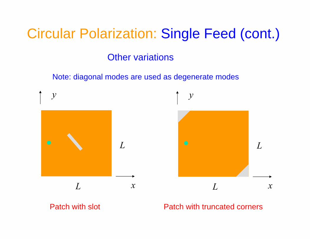
Circular Polarization: Single Feed (cont.)Other variations
L
L
x
y
Patch with slot
L
L
x
y
Patch with truncated corners
Note: diagonal modes are used as degenerate modes
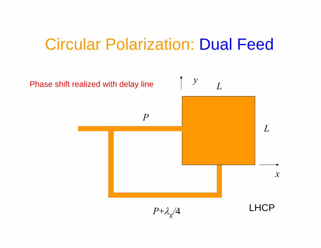
Circular Polarization: Dual Feed
L
L
x
y
P
P+λg/4 LHCP
Phase shift realized with delay line
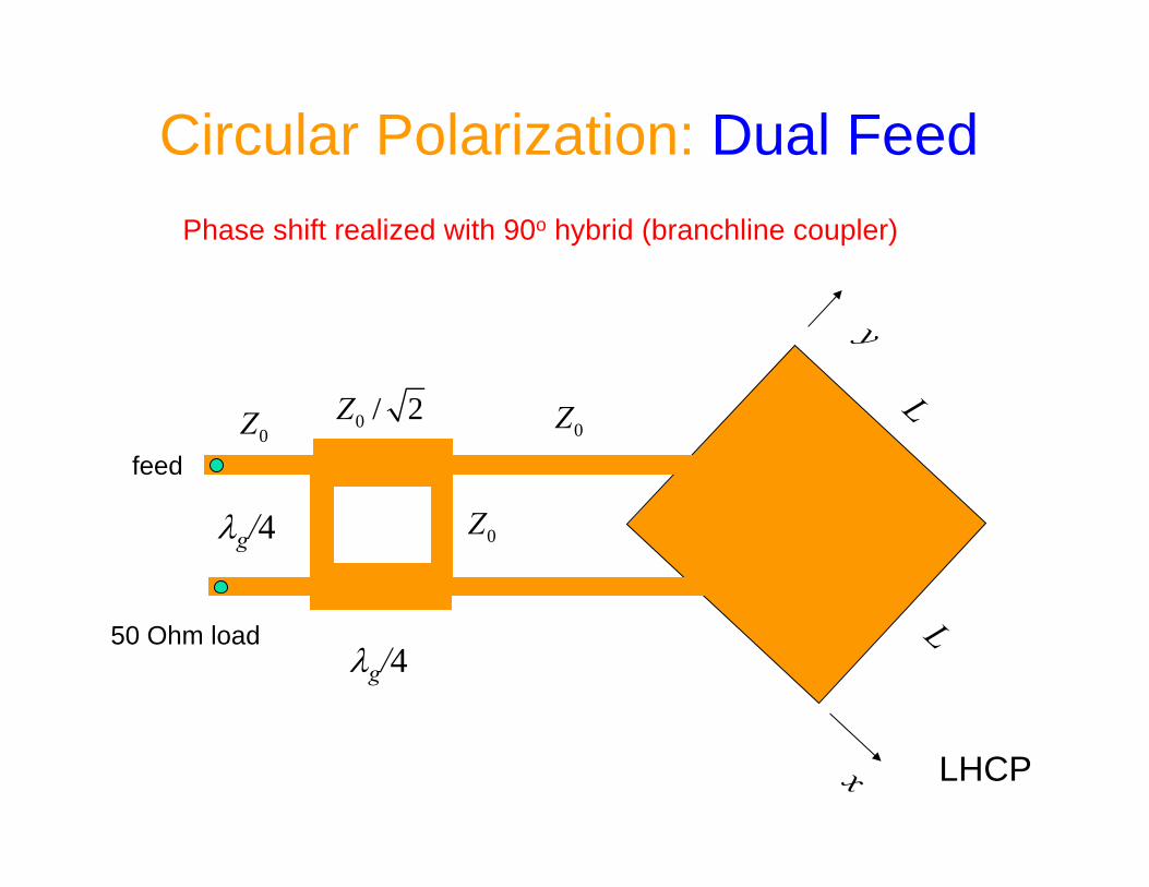
Circular Polarization: Dual FeedPhase shift realized with 90o hybrid (branchline coupler)
L
L
x
y
λg/4
LHCP
λg/4
0Z0 / 2Z
feed
50 Ohm load
0Z
0Z
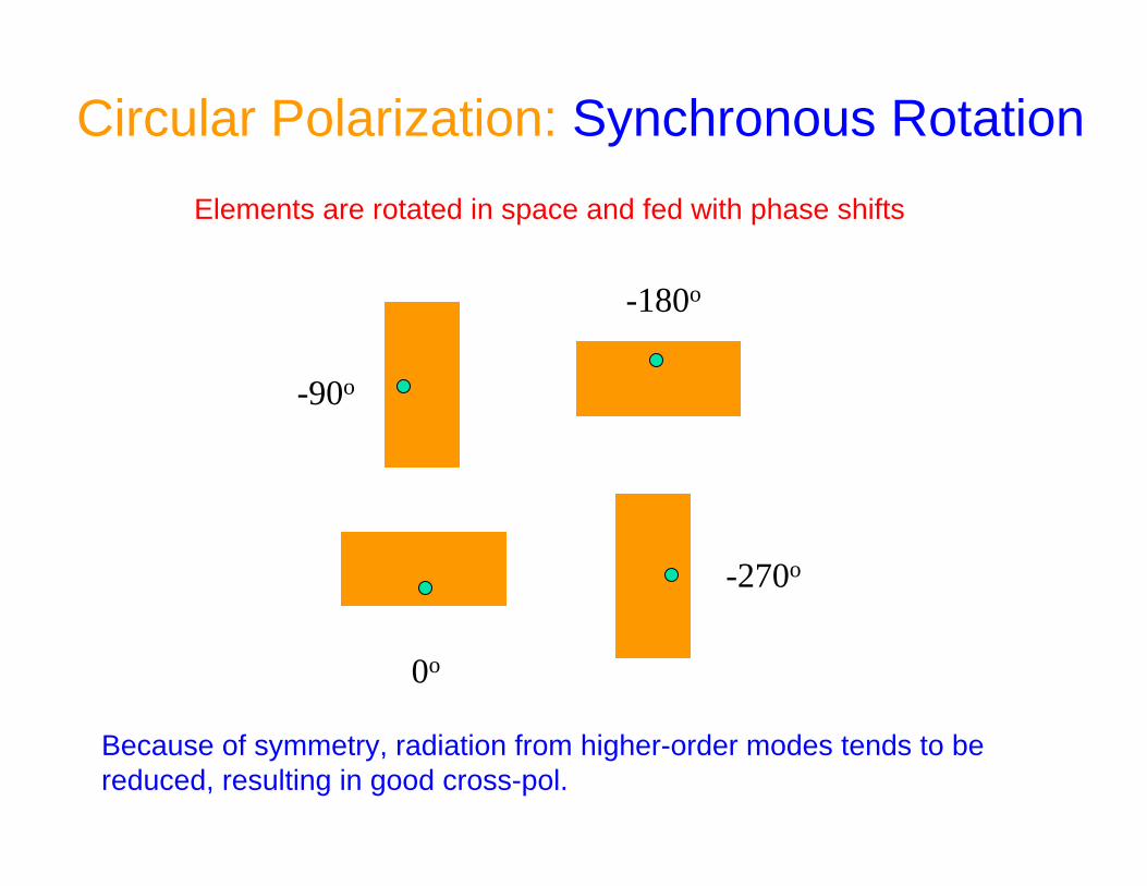
Circular Polarization: Synchronous RotationElements are rotated in space and fed with phase shifts
0o
-90o
-180o
-270o
Because of symmetry, radiation from higher-order modes tends to be reduced, resulting in good cross-pol.
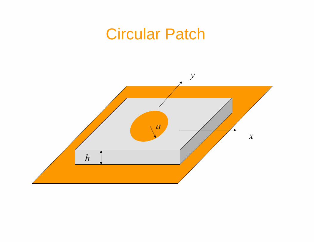
Circular Patch
x
y
h
a
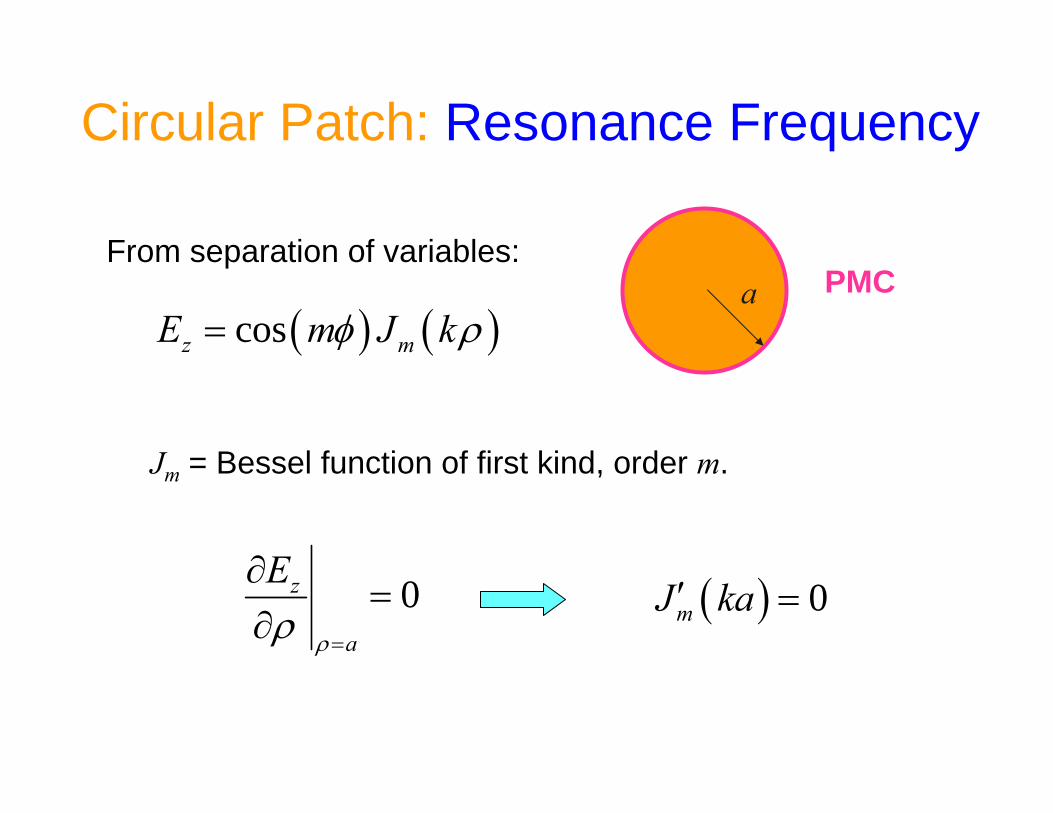
Circular Patch: Resonance Frequency
a PMCFrom separation of variables:
( ) ( )cosz mE m J kφ ρ=
Jm = Bessel function of first kind, order m.
0z
a
E
ρρ =
∂=
∂( ) 0mJ ka′ =
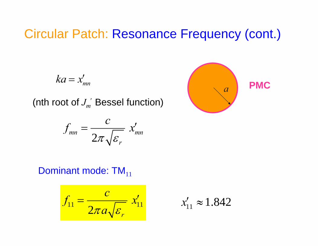
Circular Patch: Resonance Frequency (cont.)
mnka x′=a PMC
(nth root of Jm′ Bessel function)
2mn mnr
cf xπ ε
′=
Dominant mode: TM11
11 112 r
cf xaπ ε
′=11 1.842x′ ≈
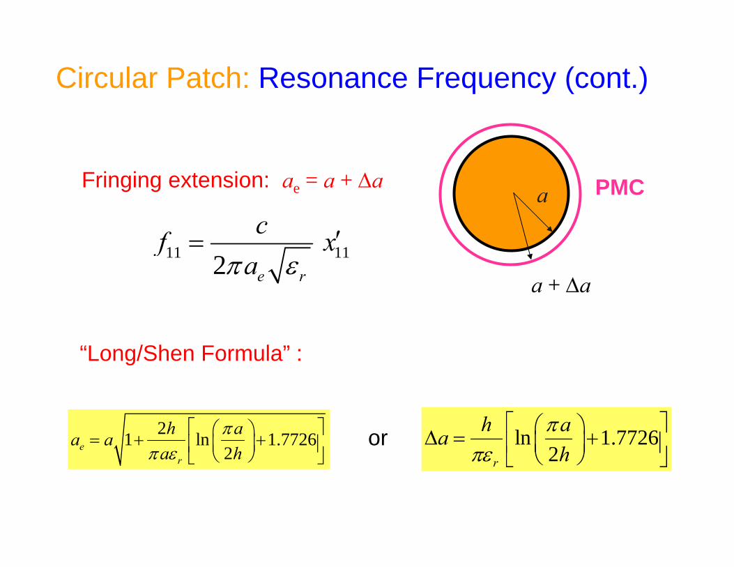
Fringing extension: ae = a + Δa
11 112 e r
cf xaπ ε
′=
“Long/Shen Formula” :
a PMC
a + Δa
ln 1.77262r
h aah
ππε
⎡ ⎤⎛ ⎞Δ = +⎜ ⎟⎢ ⎥⎝ ⎠⎣ ⎦21 ln 1.7726
2er
h aa aa h
ππ ε
⎡ ⎤⎛ ⎞= + +⎜ ⎟⎢ ⎥⎝ ⎠⎣ ⎦or
Circular Patch: Resonance Frequency (cont.)
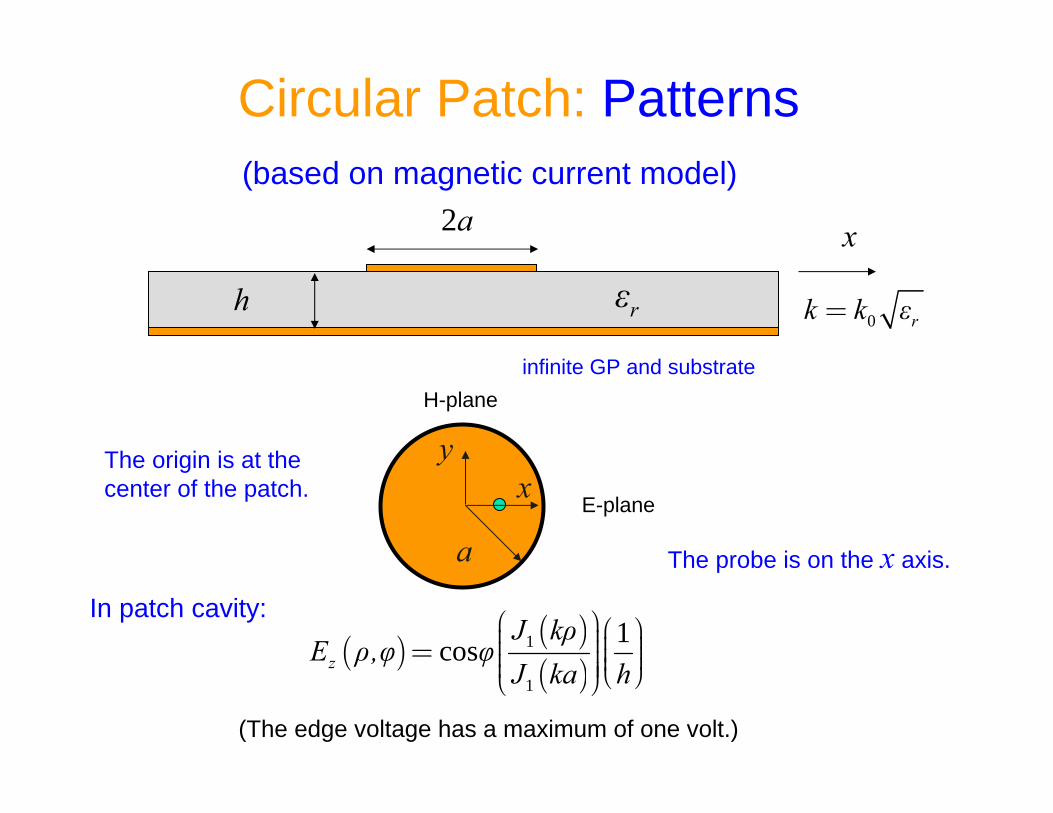
Circular Patch: Patterns(based on magnetic current model)
( )( )( )
1
1
1cosz
J kρE ρ,φ φ
J ka h
⎛ ⎞⎛ ⎞⎟⎜ ⎟⎜⎟⎜= ⎟⎜⎟⎜ ⎟⎜⎟⎟⎝ ⎠⎜⎝ ⎠
(The edge voltage has a maximum of one volt.)
a
yx
E-plane
H-plane
In patch cavity:
The probe is on the x axis.
2a
rεh
infinite GP and substrate
0 rk k ε=
x
The origin is at the center of the patch.
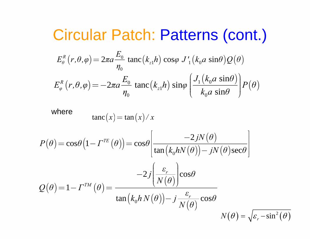
Circular Patch: Patterns (cont.)( ) ( ) ( ) ( )0
1 1 00
2 tanc cos sinRθ z
EE r,θ ,φ πa k h φ J ' k a θ Q θη
=
( ) ( )( )
( )1 001
0 0
sin2 tanc sin
sinRφ z
J k a θEE r,θ ,φ πa k h φ P θη k a θ
⎛ ⎞⎟⎜ ⎟=− ⎜ ⎟⎜ ⎟⎜⎝ ⎠
( ) ( )( ) ( )( )( ) ( )0
2cos 1 cos
tan secTE jN θ
P θ θ Γ θ θk hN θ jN θ θ
⎡ ⎤−⎢ ⎥= − = ⎢ ⎥−⎢ ⎥⎣ ⎦
( ) ( )( )
( )( )( )0
2 cos1
tan cos
r
TM
r
εj θN θ
Q θ Γ θ εk h N θ j θN θ
⎛ ⎞⎟⎜ ⎟− ⎜ ⎟⎜ ⎟⎟⎜⎝ ⎠= − =
−
( ) ( )tanc tanx x / x=where
( ) ( )2sinrN θ ε θ= −
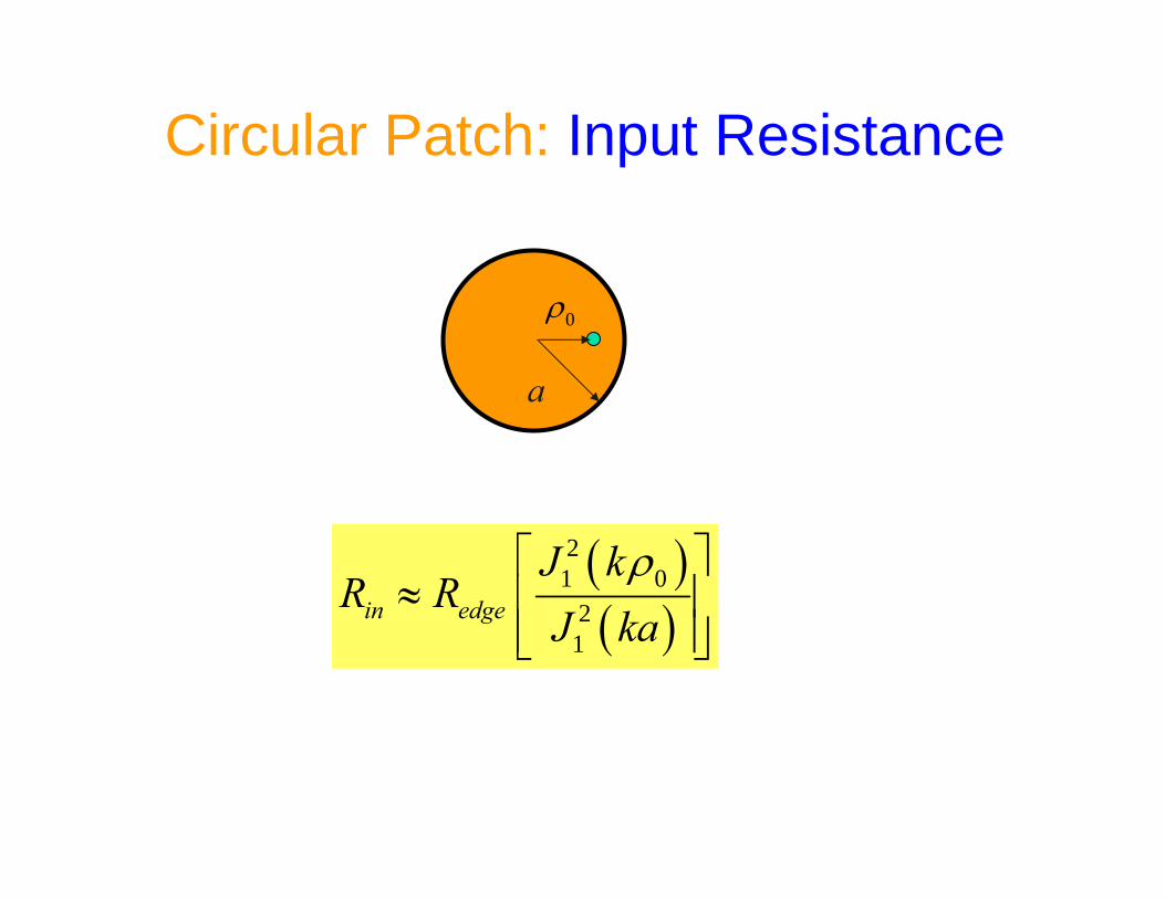
Circular Patch: Input Resistance
( )( )
21 0
21
in edge
J kR R
J kaρ⎡ ⎤
≈ ⎢ ⎥⎢ ⎥⎣ ⎦
a
0ρ
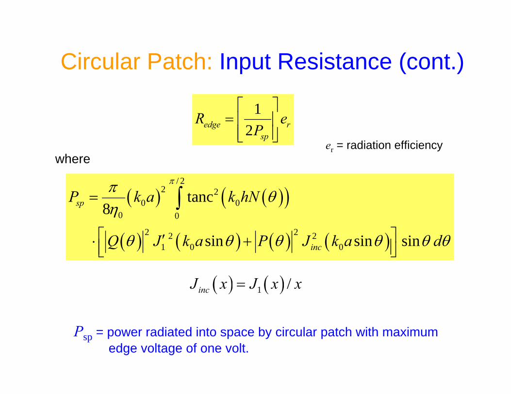
Circular Patch: Input Resistance (cont.)
12edge r
sp
R eP
⎡ ⎤= ⎢ ⎥
⎢ ⎥⎣ ⎦
( ) ( )( )
( ) ( ) ( ) ( )
/ 22 2
0 00 0
2 22 21 0 0
tanc8
sin sin sin
sp
inc
P k a k hN
Q J k a P J k a d
ππ θη
θ θ θ θ θ θ
=
⎡ ⎤′⋅ +⎢ ⎥⎣ ⎦
∫
( ) ( )1 /incJ x J x x=
where
Psp = power radiated into space by circular patch with maximum edge voltage of one volt.
er = radiation efficiency
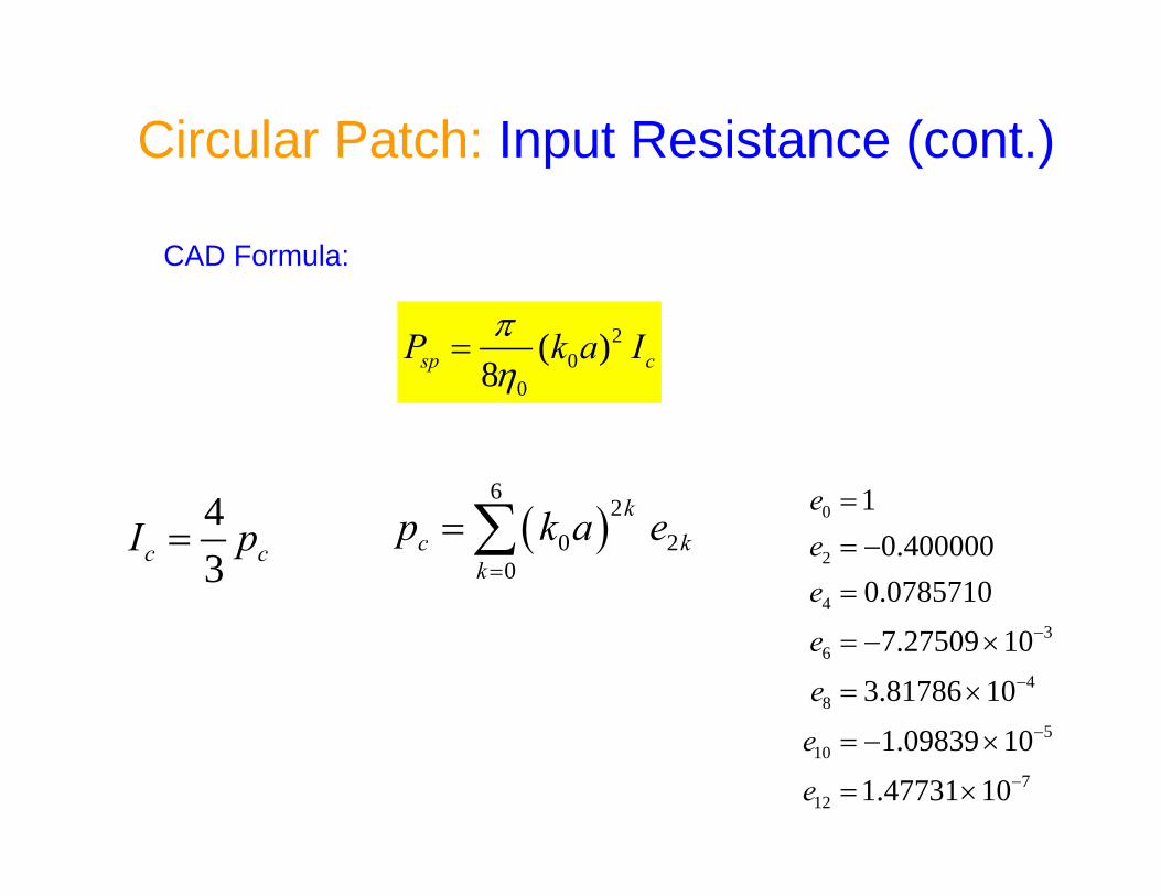
Circular Patch: Input Resistance (cont.)
20
0
( )8sp cP k a Iπη
=
CAD Formula:
43c cI p= ( )
62
0 20
kc k
k
p k a e=
= ∑ 0
2
43
64
85
107
12
10.400000
0.0785710
7.27509 10
3.81786 10
1.09839 10
1.47731 10
eee
e
e
e
e
−
−
−
−
== −=
= − ×
= ×
= − ×
= ×
Feeding Methods
Some of the more common methods for feeding microstrip antennas are shown.
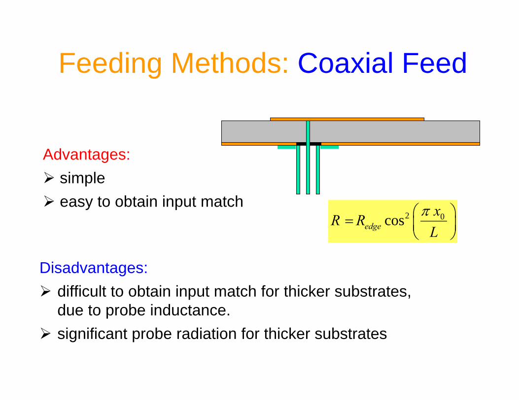
Feeding Methods: Coaxial Feed
Advantages:simple easy to obtain input match
Disadvantages: difficult to obtain input match for thicker substrates, due to probe inductance. significant probe radiation for thicker substrates
2 0cosedgexR R
Lπ⎛ ⎞= ⎜ ⎟
⎝ ⎠
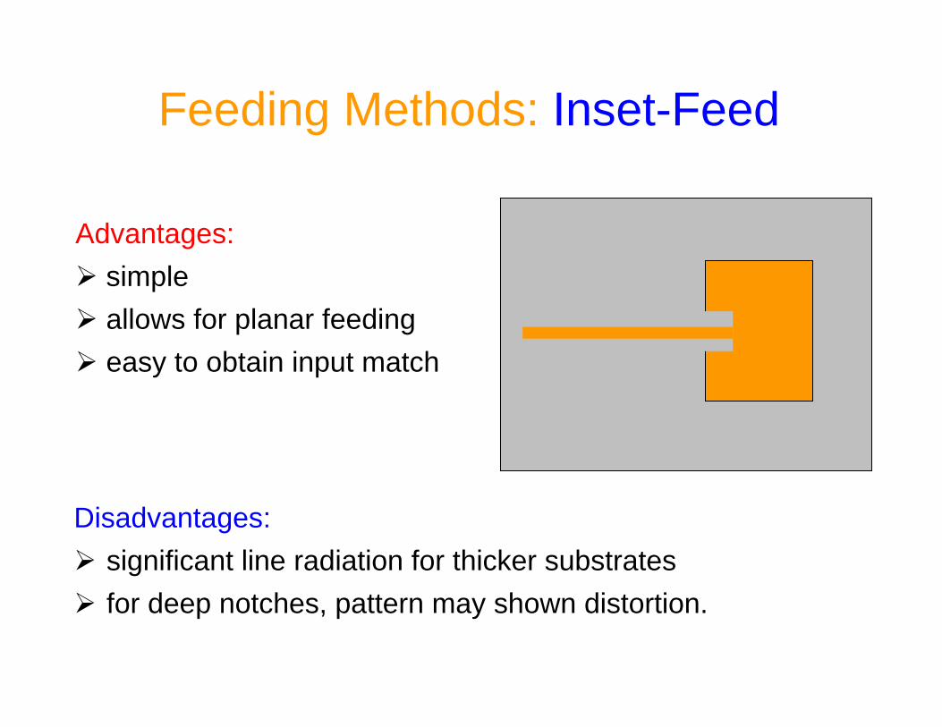
Feeding Methods: Inset-Feed
Advantages:simpleallows for planar feeding easy to obtain input match
Disadvantages: significant line radiation for thicker substratesfor deep notches, pattern may shown distortion.
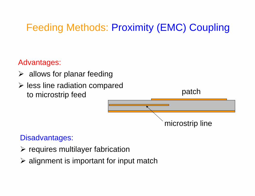
Feeding Methods: Proximity (EMC) Coupling
Advantages:allows for planar feeding less line radiation compared to microstrip feed
Disadvantages:requires multilayer fabricationalignment is important for input match
patch
microstrip line
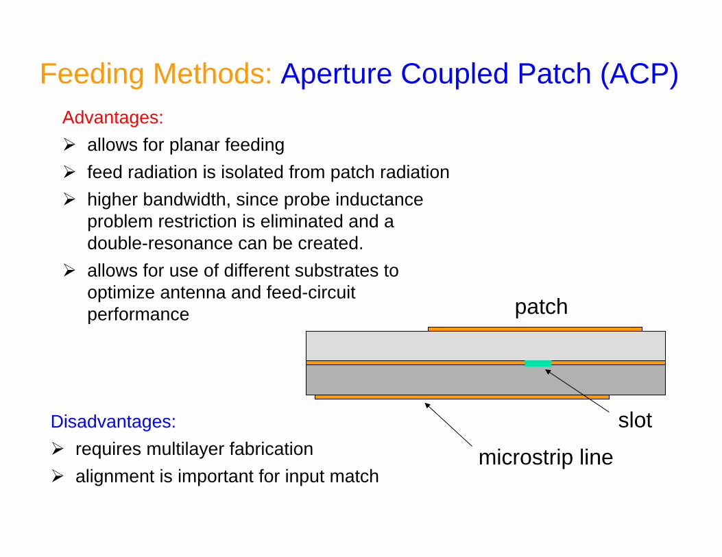
Feeding Methods: Aperture Coupled Patch (ACP) Advantages:
allows for planar feeding feed radiation is isolated from patch radiationhigher bandwidth, since probe inductance problem restriction is eliminated and a double-resonance can be created.allows for use of different substrates to optimize antenna and feed-circuit performance
Disadvantages: requires multilayer fabricationalignment is important for input match
patch
microstrip line
slot

Improving Bandwidth
Some of the techniques that has been successfully developed are illustrated here.
(The literature may be consulted for additional designs and modifications.)
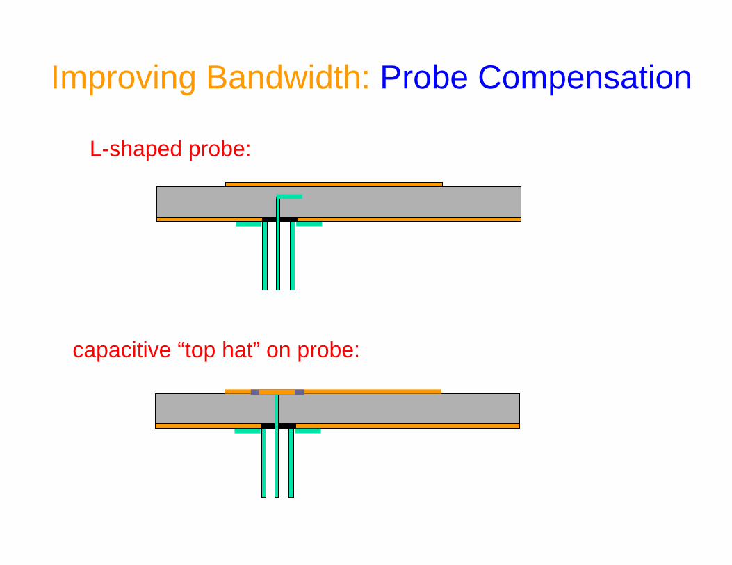
Improving Bandwidth: Probe Compensation
L-shaped probe:
capacitive “top hat” on probe:
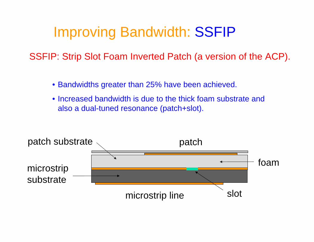
Improving Bandwidth: SSFIPSSFIP: Strip Slot Foam Inverted Patch (a version of the ACP).
microstrip substrate
patch
microstrip line slot
foam
patch substrate
• Bandwidths greater than 25% have been achieved.
• Increased bandwidth is due to the thick foam substrate and also a dual-tuned resonance (patch+slot).
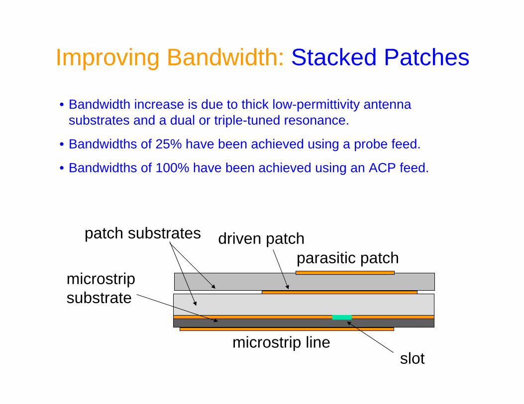
Improving Bandwidth: Stacked Patches
• Bandwidth increase is due to thick low-permittivity antenna substrates and a dual or triple-tuned resonance.
• Bandwidths of 25% have been achieved using a probe feed.
• Bandwidths of 100% have been achieved using an ACP feed.
microstrip substrate
driven patch
microstrip lineslot
patch substratesparasitic patch
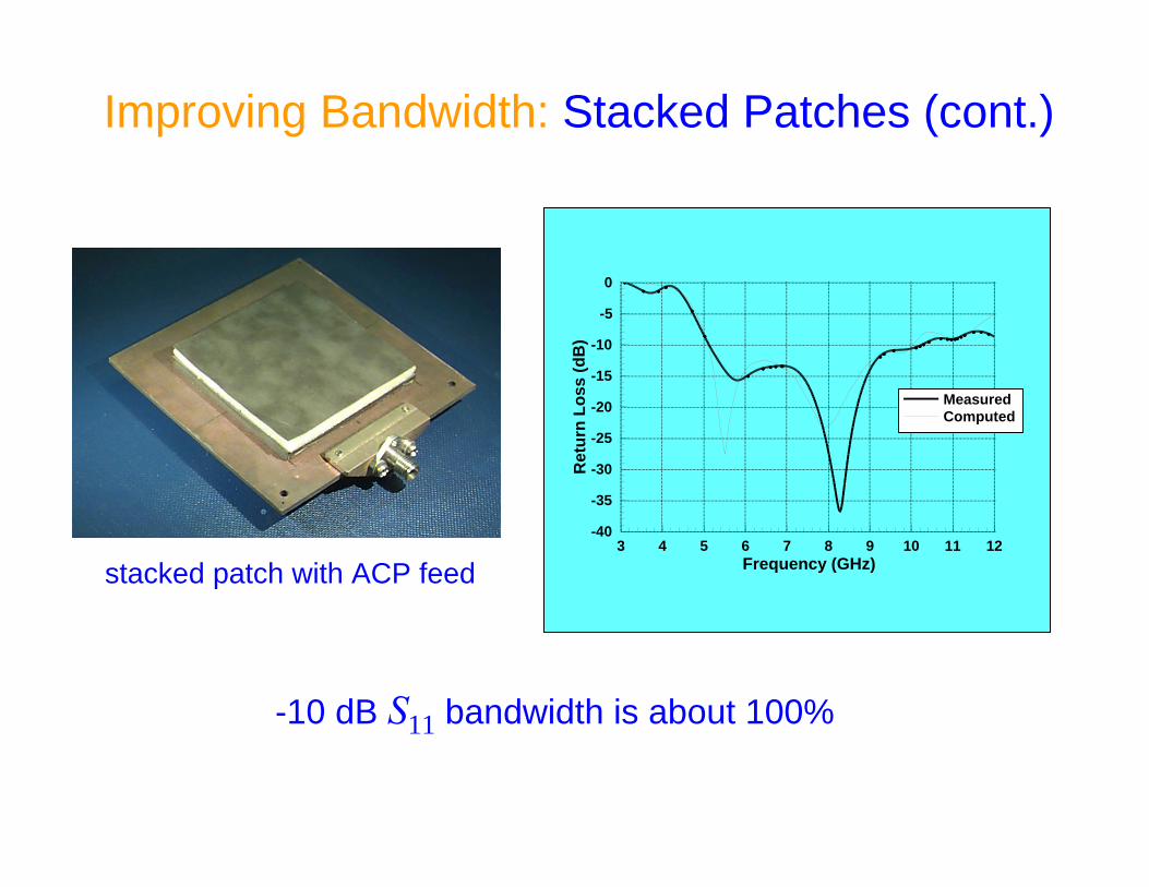
Improving Bandwidth: Stacked Patches (cont.)
-10 dB S11 bandwidth is about 100%
stacked patch with ACP feed3 4 5 6 7 8 9 10 11 12
Frequency (GHz)
-40
-35
-30
-25
-20
-15
-10
-5
0
Ret
urn
Loss
(dB
)
MeasuredComputed
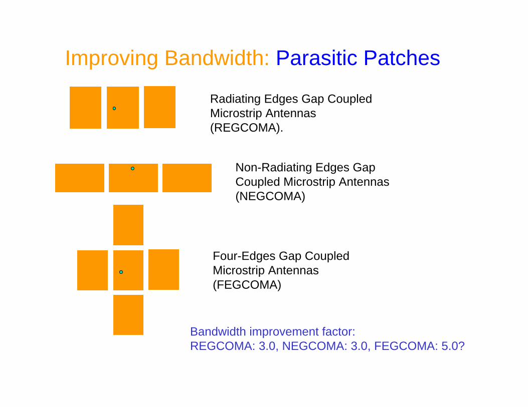
Improving Bandwidth: Parasitic Patches
Radiating Edges Gap Coupled Microstrip Antennas (REGCOMA).
Non-Radiating Edges Gap Coupled Microstrip Antennas (NEGCOMA)
Four-Edges Gap Coupled Microstrip Antennas (FEGCOMA)
Bandwidth improvement factor:REGCOMA: 3.0, NEGCOMA: 3.0, FEGCOMA: 5.0?
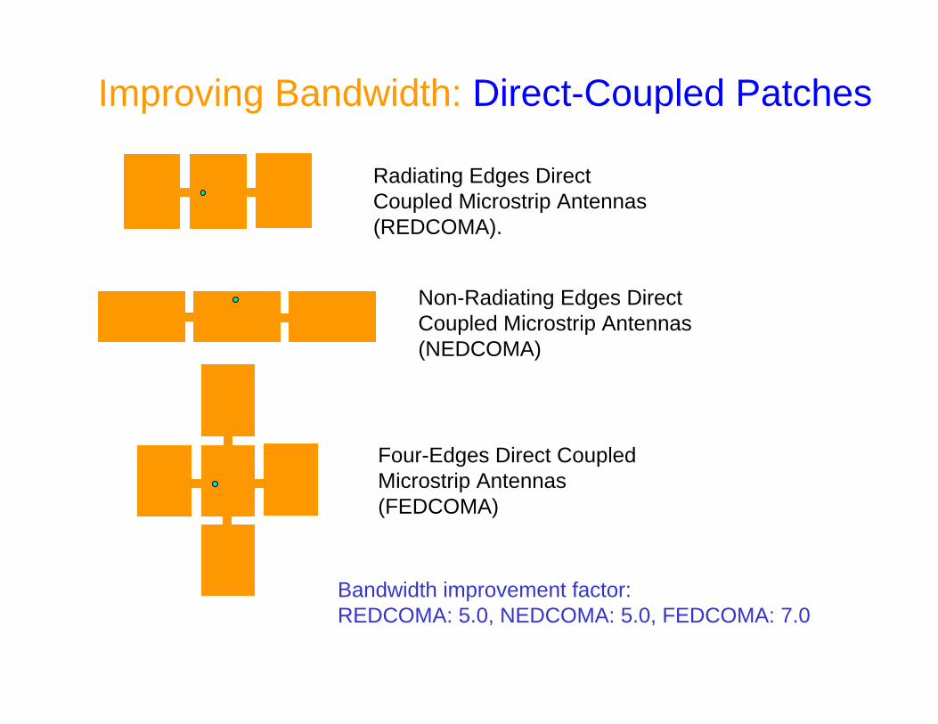
Improving Bandwidth: Direct-Coupled Patches
Radiating Edges Direct Coupled Microstrip Antennas (REDCOMA).
Non-Radiating Edges Direct Coupled Microstrip Antennas (NEDCOMA)
Four-Edges Direct Coupled Microstrip Antennas (FEDCOMA)
Bandwidth improvement factor:REDCOMA: 5.0, NEDCOMA: 5.0, FEDCOMA: 7.0
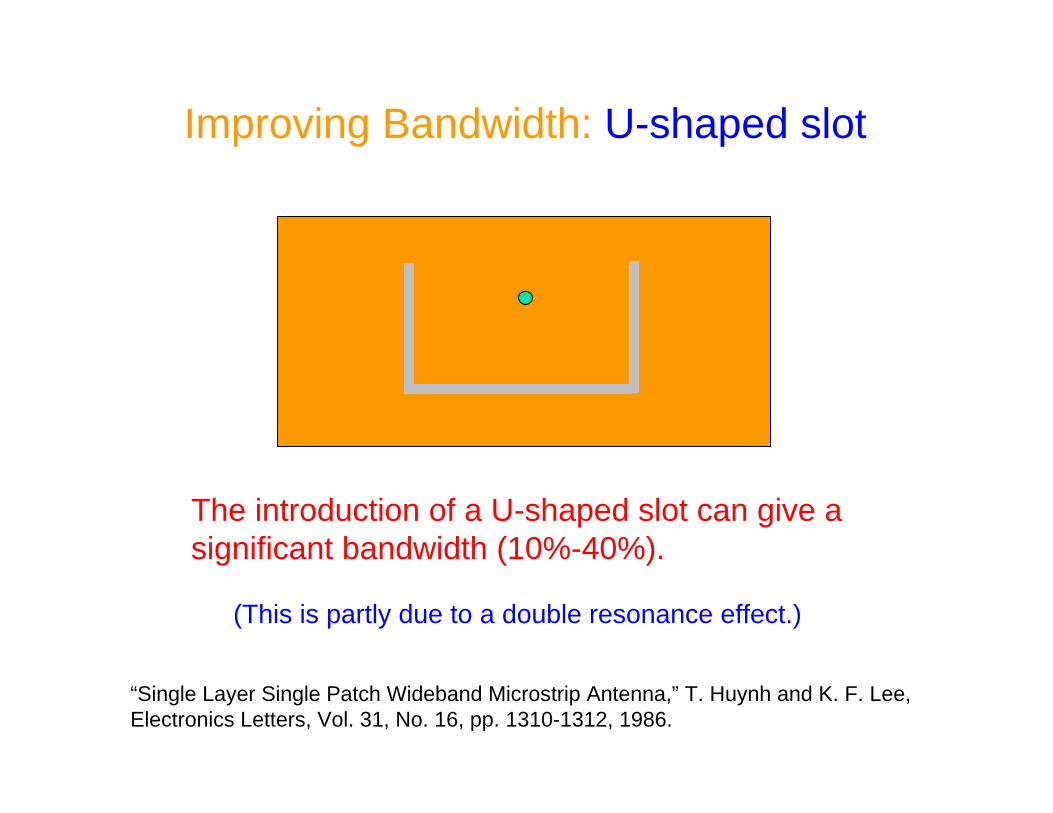
Improving Bandwidth: U-shaped slot
The introduction of a U-shaped slot can give a significant bandwidth (10%-40%).
(This is partly due to a double resonance effect.)
“Single Layer Single Patch Wideband Microstrip Antenna,” T. Huynh and K. F. Lee, Electronics Letters, Vol. 31, No. 16, pp. 1310-1312, 1986.
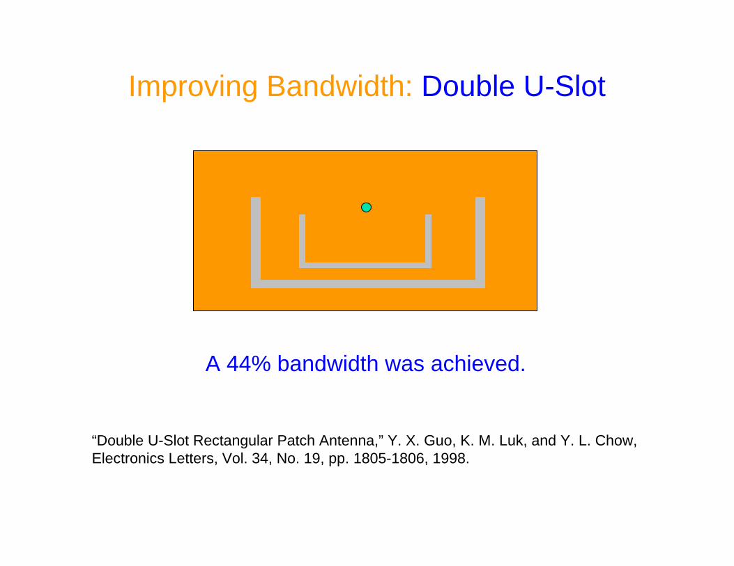
Improving Bandwidth: Double U-Slot
A 44% bandwidth was achieved.
“Double U-Slot Rectangular Patch Antenna,” Y. X. Guo, K. M. Luk, and Y. L. Chow, Electronics Letters, Vol. 34, No. 19, pp. 1805-1806, 1998.
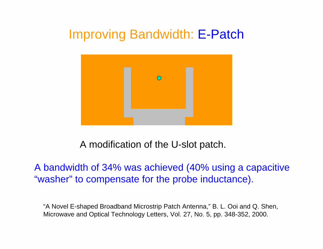
Improving Bandwidth: E-Patch
A modification of the U-slot patch.
A bandwidth of 34% was achieved (40% using a capacitive “washer” to compensate for the probe inductance).
“A Novel E-shaped Broadband Microstrip Patch Antenna,” B. L. Ooi and Q. Shen, Microwave and Optical Technology Letters, Vol. 27, No. 5, pp. 348-352, 2000.
Multi-Band Antennas
General Principle:
Introduce multiple resonance paths into the antenna. (The same technique can be used to increase bandwidth via multiple resonances, if the resonances are closely spaced.)
A multi-band antenna is often more desirable than a broad-band antenna, if multiple narrow-band channels are to be covered.
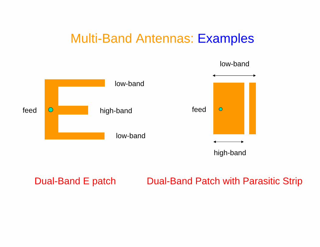
Multi-Band Antennas: Examples
Dual-Band E patch
high-band
low-band
low-band
feed
Dual-Band Patch with Parasitic Strip
low-band
high-band
feed
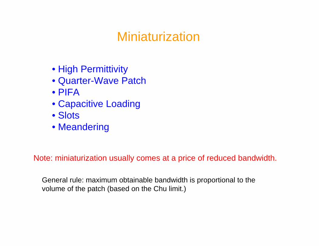
Miniaturization
• High Permittivity• Quarter-Wave Patch• PIFA• Capacitive Loading• Slots• Meandering
Note: miniaturization usually comes at a price of reduced bandwidth.
General rule: maximum obtainable bandwidth is proportional to the volume of the patch (based on the Chu limit.)
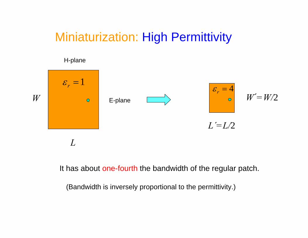
Miniaturization: High Permittivity
It has about one-fourth the bandwidth of the regular patch.
L
W E-plane
H-plane
1rε =4rε =
L´=L/2
W´=W/2
(Bandwidth is inversely proportional to the permittivity.)
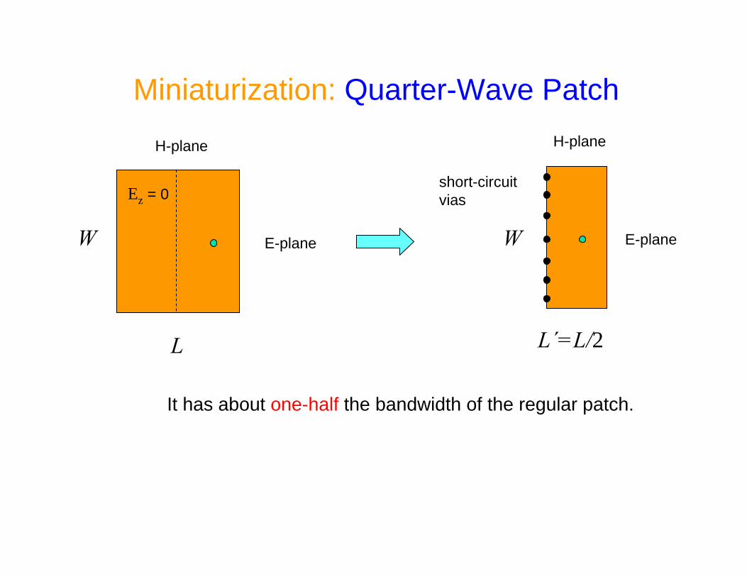
Miniaturization: Quarter-Wave Patch
L
W E-plane
H-plane
Ez = 0
It has about one-half the bandwidth of the regular patch.
W E-plane
H-plane
short-circuit vias
L´=L/2
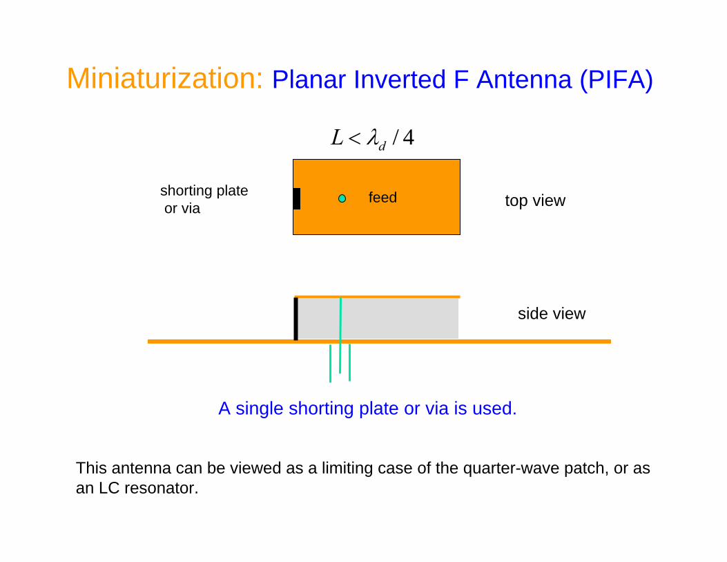
Miniaturization: Planar Inverted F Antenna (PIFA)
A single shorting plate or via is used.
This antenna can be viewed as a limiting case of the quarter-wave patch, or as an LC resonator.
side view
feedshorting plateor via top view
/ 4dL λ<
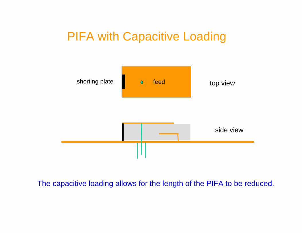
PIFA with Capacitive Loading
The capacitive loading allows for the length of the PIFA to be reduced.
feedshorting plate top view
side view
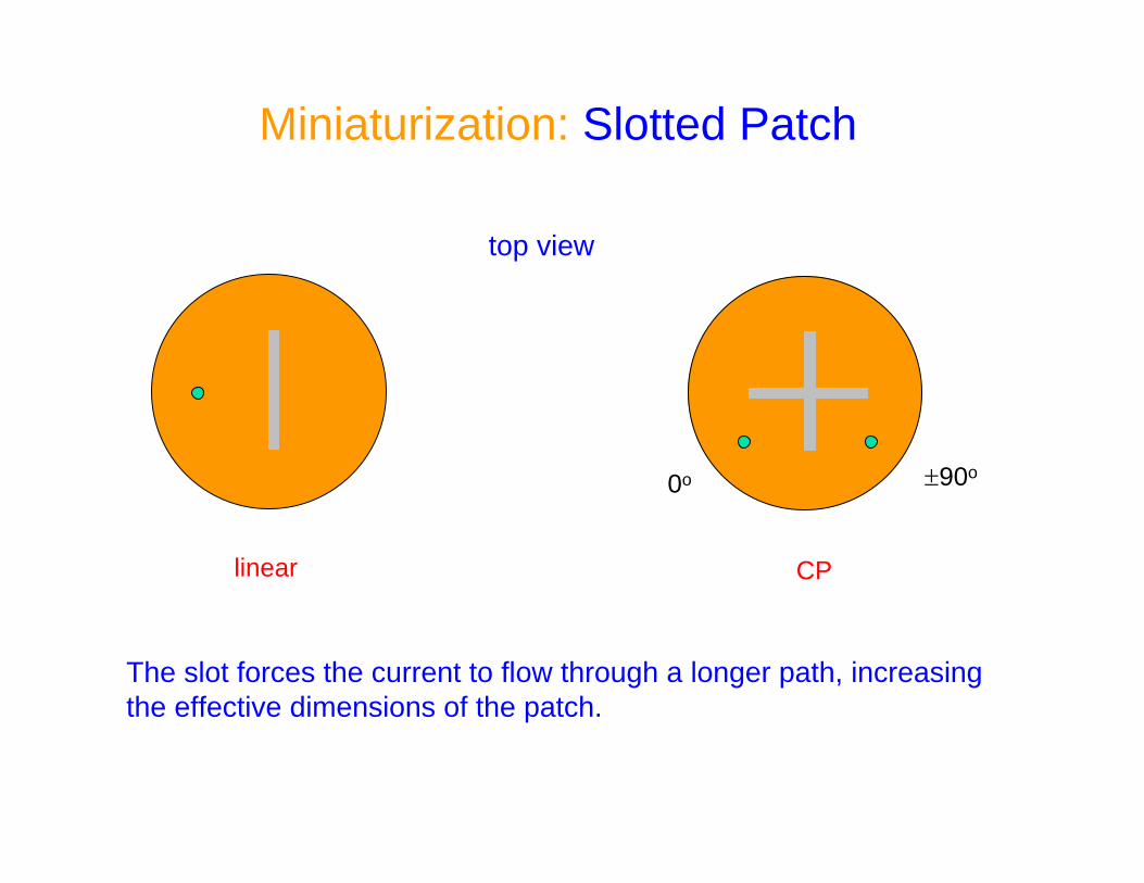
Miniaturization: Slotted Patch
The slot forces the current to flow through a longer path, increasing the effective dimensions of the patch.
top view
linear CP
0o ±90o
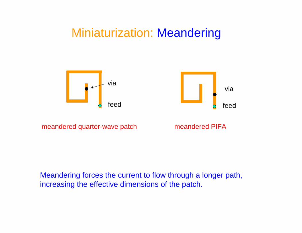
Miniaturization: Meandering
Meandering forces the current to flow through a longer path, increasing the effective dimensions of the patch.
feed
via
meandered quarter-wave patch
feed
via
meandered PIFA
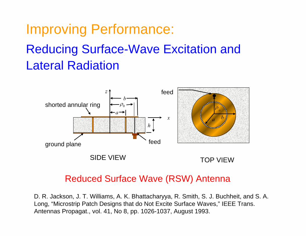
Improving Performance: Reducing Surface-Wave Excitation and Lateral Radiation
Reduced Surface Wave (RSW) Antenna
SIDE VIEW
zb
hx
shorted annular ring
ground plane feed
aρ0
TOP VIEW
a
ρo
b
feed
D. R. Jackson, J. T. Williams, A. K. Bhattacharyya, R. Smith, S. J. Buchheit, and S. A. Long, “Microstrip Patch Designs that do Not Excite Surface Waves,” IEEE Trans. Antennas Propagat., vol. 41, No 8, pp. 1026-1037, August 1993.
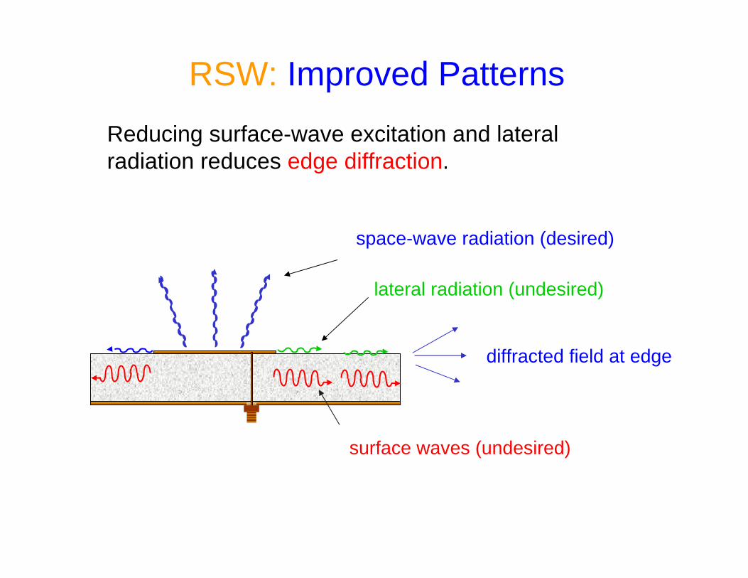
Reducing surface-wave excitation and lateral radiation reduces edge diffraction.
RSW: Improved Patterns
space-wave radiation (desired)
lateral radiation (undesired)
surface waves (undesired)
diffracted field at edge
-90
-60
-30
0
30
60
90
120
150
180
210
240
-40
-30
-30
-20
-20
-10
-10-90
-60
-30
0
30
60
90
120
150
180
210
240
-40
-30
-30
-20
-20
-10
-10
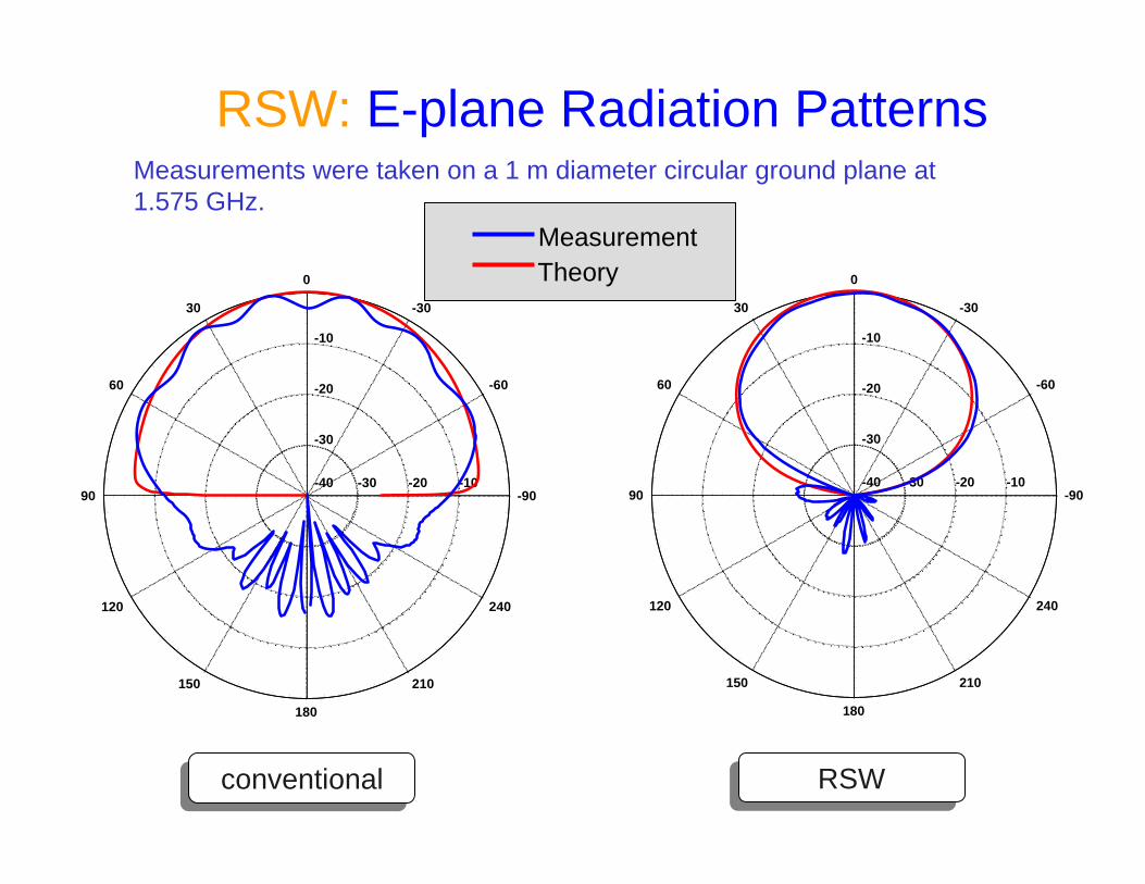
conventionalconventional RSWRSW
Measurements were taken on a 1 m diameter circular ground plane at 1.575 GHz.
RSW: E-plane Radiation Patterns
MeasurementTheory
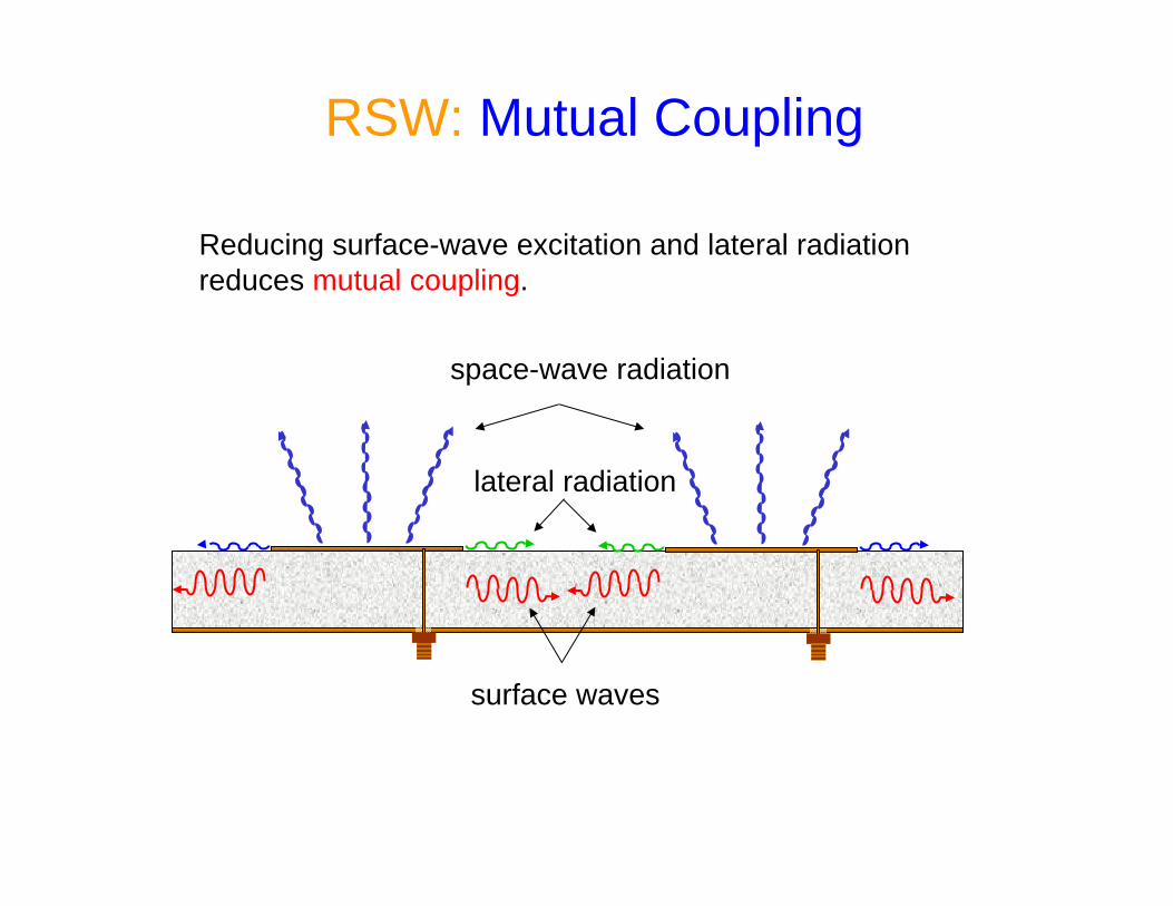
Reducing surface-wave excitation and lateral radiation reduces mutual coupling.
RSW: Mutual Coupling
space-wave radiation
lateral radiation
surface waves
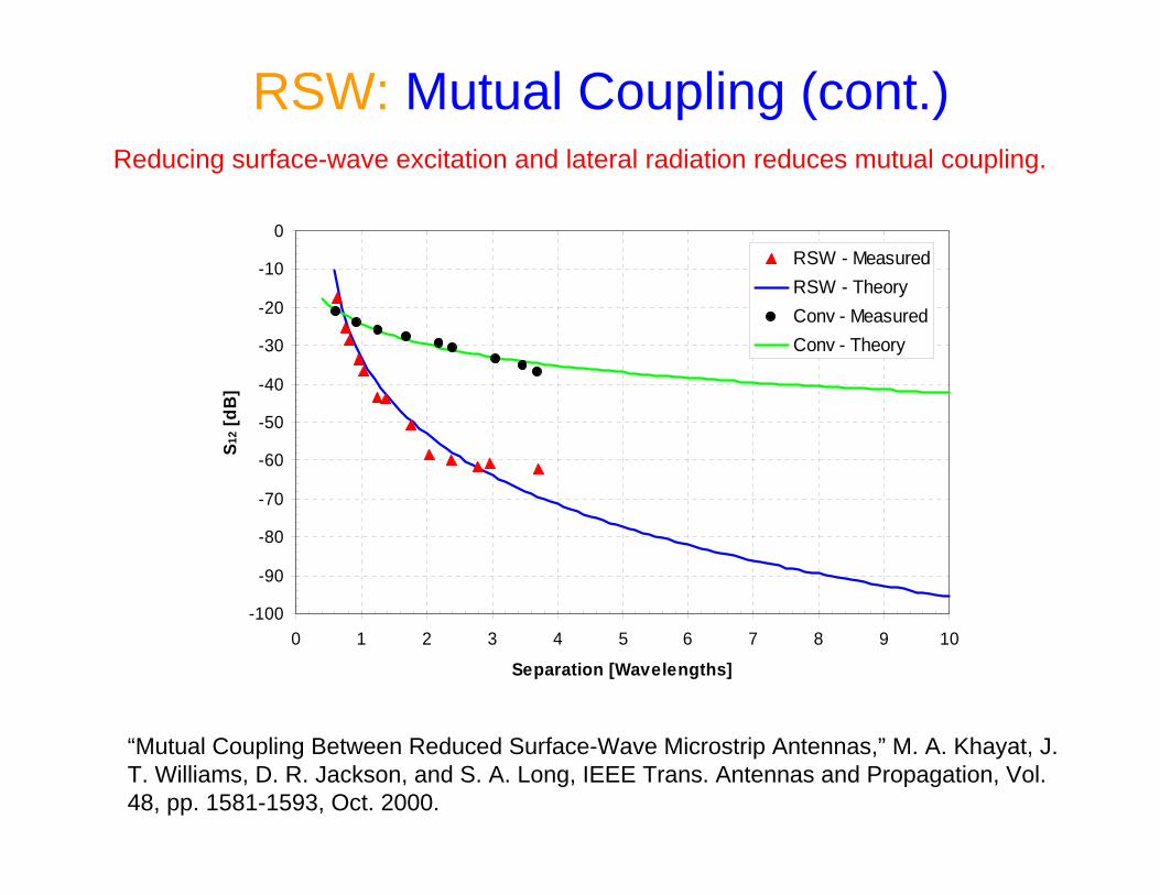
Reducing surface-wave excitation and lateral radiation reduces mutual coupling.
-100
-90
-80
-70
-60
-50
-40
-30
-20
-10
0
0 1 2 3 4 5 6 7 8 9 10
Separation [Wavelengths]
S12 [
dB]
RSW - MeasuredRSW - TheoryConv - MeasuredConv - Theory
RSW: Mutual Coupling (cont.)
“Mutual Coupling Between Reduced Surface-Wave Microstrip Antennas,” M. A. Khayat, J. T. Williams, D. R. Jackson, and S. A. Long, IEEE Trans. Antennas and Propagation, Vol. 48, pp. 1581-1593, Oct. 2000.
ReferencesGeneral references about microstrip antennas:
Microstrip Antenna Design Handbook, R. Garg, P. Bhartia, I. J. Bahl, and A. Ittipiboon, Editors, Artech House, 2001.
Microstrip Patch Antennas: A Designer’s Guide, Rodney B. Waterhouse, Kluwer Academic Publishers, 2003.
Microstrip and Printed Antenna Design, Randy Bancroft, Noble Publishers, 2004.
Microstrip Antennas: The Analysis and Design of Microstrip Antennas and Arrays, David M. Pozar and Daniel H. Schaubert, Editors, Wiley/IEEE Press, 1995.
Advances in Microstrip and Printed Antennas, K. F. Lee, Editor, John Wiley, 1997.
References (cont.)
General references about microstrip antennas (cont.):
Millimeter-Wave Microstrip and Printed Circuit Antennas, P. Bhartia, Artech House, 1991.
The Handbook of Microstrip Antennas (two volume set), J. R. James and P. S. Hall, INSPEC, 1989.
Microstrip Antenna Theory and Design, J. R. James, P. S. Hall, and C. Wood, INSPEC/IEE, 1981.
Computer-Aided Design of Rectangular Microstrip Antennas, D. R. Jackson, S. A. Long, J. T. Williams, and V. B. Davis, Ch. 5 of Advances in Microstrip and Printed Antennas, K. F. Lee, Editor, John Wiley, 1997.
More information about the CAD formulas presented here for the rectangular patch may be found in:
References (cont.)
References devoted to broadband microstrip antennas:
Compact and Broadband Microstrip Antennas, Kin-Lu Wong, John Wiley, 2003.
Broadband Microstrip Antennas, Girish Kumar and K. P. Ray, Artech House, 2002.
Broadband Patch Antennas, Jean-Francois Zurcher and Fred E. Gardiol, Artech House, 1995.
References (cont.)