Embed Size (px)
Citation preview
Paulo Alexandre Valente de Jesus Rosa
Mestre em Engenharia do Ambiente
Minimal Computation Structures for Visual Information Applications based
on Printed Electronics
Dissertação para obtenção do Grau de Doutor em Media Digitais
Orientador: António da Nóbrega de Sousa da Câmara, Professor Catedrático, Faculdade de Ciências e
Tecnologia da Universidade Nova de Lisboa
Dezembro, 2015

- Blank Page -
New University of Lisbon
Faculty of Sciences and Technology
Minimal Computation Structures for
Visual Information Applications based on
Printed Electronics
Paulo Alexandre Valente de Jesus Rosa
Submitted to the Faculty of Sciences and Technology of the New University of
Lisbon, in accordance with the requirements for the degree of
Doctor of Philosophy in Digital Media
Supervisor:
António da Nóbrega de Sousa da Câmara, Cathedratic Professor
Faculty of Sciences and Technology of the New University of Lisbon
Lisbon, 2015

- Blank Page -

Acknowledgments
Looking back, it is perceptible how these last years have been quite of a
journey. Along the way, there were many colleagues and friends who would always
had the time to help me and support me. I want to express my profound gratitude
to each one of you.
Foremost, I would like to express my deepest thanks to my supervisor,
Professor António Câmara, for his continual support, advice, knowledge and
motivation. His mentorship was fundamental for the finalisation of this thesis.
I would also like to thank the members of my dissertation committee, not
only for their time and excellent feedback but also for their encouragements:
thanks to Cristina Gouveia and Inês Henriques. You always provided me the
support I needed.
I am also deeply grateful to have worked with several motivated and talented
people. Part of the research work presented in this thesis was done in cooperation
with Ynvisible, a leading developer of electrochromic displays. I fully thank to all the
present and past members of Ynvisible. A special thanks to Ana Marques, Sofia
Martins, Lucia Gomes, Aida Branco, Soraia Assunção, Nuno Nascimento, Ricardo
Silva, Mario Simões, João Ricardo, Jorge Araújo, Cláudia Costa and Carlos Pinheiro.
Their support was crucial in the development and fabrication of the various
electrochromic displays used throughout my research.
I would like to extend my appreciation to the Center for Environmental and
Sustainability Research of the Faculty of Sciences and Technology of the New
University of Lisbon for receiving me as well as the UT Austin-Portugal Doctoral
Program for its support. To the Photochemistry and Supramolecular Chemistry
research group of the Department of Chemistry of the Faculty of Sciences and
Technology goes also my thank you, in particular to Professor Fernando Pina and
Professor Jorge Parola for their help in the early stages of this Ph.D.

I would also like to acknowledge the Portuguese Foundation for Science and
Technology (FCT-MCTES). This research work was supported by a 4-year fellowship
from this organization without which it would not be possible.
A special mention to Ângela Guimarães Pereira for her helpfulness, support
and encouragement. This journey certainly stated with her convincing me to enrol
in such endeavour.
I take this opportunity to thank as well to my family for their constant support
and encouragement. Naturally, a special thank you to my parents and my sister for
their love as well as for supporting all the ventures I had over the last years.
Finally, I dedicate this thesis to Ana. Thank you for your patience and for
always believing in me. I undoubtedly could not have done it without you by my
side.
Thank you!
Abstract
In the early nineties, Mark Weiser wrote a series of seminal papers that
introduced the concept of Ubiquitous Computing. According to Weiser, computers
require too much attention from the user, drawing his focus from the tasks at hand.
Instead of being the centre of attention, computers should be so natural that they
would vanish into the human environment. Computers become not only truly
pervasive but also effectively invisible and unobtrusive to the user. This requires
not only for smaller, cheaper and low power consumption computers, but also for
equally convenient display solutions that can be harmoniously integrated into our
surroundings. With the advent of Printed Electronics, new ways to link the physical
and the digital worlds became available. By combining common printing techniques
such as inkjet printing with electro-optical functional inks, it is starting to be
possible not only to mass-produce extremely thin, flexible and cost effective
electronic circuits but also to introduce electronic functionalities into products where
it was previously unavailable. Indeed, Printed Electronics is enabling the creation of
novel sensing and display elements for interactive devices, free of form factor. At
the same time, the rise in the availability and affordability of digital fabrication
technologies, namely of 3D printers, to the average consumer is fostering a new
industrial (digital) revolution and the democratisation of innovation. Nowadays,
end-users are already able to custom design and manufacture on demand their own
physical products, according to their own needs. In the future, they will be able to
fabricate interactive digital devices with user-specific form and functionality from
the comfort of their homes.
This thesis explores how task-specific, low computation, interactive devices
capable of presenting dynamic visual information can be created using Printed
Electronics technologies, whilst following an approach based on the ideals behind
Personal Fabrication. Focus is given on the use of printed electrochromic displays as
a medium for delivering dynamic digital information. According to the architecture
of the displays, several approaches are highlighted and categorised. Furthermore, a
pictorial computation model based on extended cellular automata principles is used

to programme dynamic simulation models into matrix-based electrochromic
displays. Envisaged applications include the modelling of physical, chemical,
biological, and environmental phenomena.
Resumo
No início dos anos noventa, Mark Weiser escreveu uma série de artigos que
introduziram o conceito de Ubiquitous Computing. De acordo com Weiser, os
computadores requerem demasiada atenção do utilizador, desviando o seu foco das
tarefas em mão. Em vez de serem o centro das atenções, os computadores
deveriam ser naturais ao ponto de desaparecerem no meio humano. Passamos
então a ter computadores verdadeiramente omnipresentes mas também
completamente discretos e intuitivos. Para tal, é necessário ter computadores mais
pequenos, mais baratos e com consumos de energia menores, mas também
soluções de ecrãs igualmente convenientes que possam ser integradas
harmoniosamente no nosso meio. Com o recente aparecimento da Eletrónica
Impressa, novas formas de ligar o meio físico e o digital ficaram disponíveis. Ao se
combinar técnicas de impressão comuns tais como a impressão a jacto de tinta com
tintas funcionais eletro-ópticas, passou a ser possível produzir em grande escala
circuitos eletrónicos extremamente finos, flexíveis e de baixo custo, assim como
introduzir funcionalidades electrónicas em produtos onde até agora não era possível
devido. Sem dúvida, a eletrónica impressa veio permitir a criação de elementos
inovativos para dispositivos interativos, livres de um formato predefinido. Ao
mesmo tempo, o aumento da disponibilidade e acessibilidade das tecnologias de
fabrico digital, em particular de impressoras 3D, ao consumidor médio está a
promover uma nova revolução industrial (digital) e a incitar a democratização da
inovação. Actualmente, qualquer pessoa já pode projectar os seus próprios
produtos físicos, de acordo com suas necessidades, e fabrica-los sob pedido. No
futuro, será o fabrico de dispositivos digitais interativos com formato e
funcionalidade específicas que será possível de ser feito a partir do conforto das
nossas casas.
Esta tese explora como dispositivos interativos de baixa computação capazes
de apresentar informação visual dinâmica podem ser criados utilizando tecnologias
de eletrônica impressa e adoptando uma abordagem baseada nos princípios do
fabrico pessoal. É dado foco ao uso de ecrãs electrocrómicos impressos como o

meio de transmissão de informação digital dinâmica. De acordo com a arquitectura
dos ecrãs, várias abordagens são destacadas e categorizadas. Um modelo de
computação pictórica baseada nos princípios dos autómatos celulares é
posteriormente utilizado para programar modelos de simulação dinâmicos em ecrãs
electrocrómicos matriciais. As aplicações previstas incluem a modelação de
fenómenos físicos, químicos, biológicos e ambientais.
9
Table of Contents
1
Introduction ......................................................................................... 23
1.1 The world is the next interface ......................................................... 23
1.2 What is wrong with the computer? .................................................... 24
1.3 Objective: Invisible technology ......................................................... 25
1.4 Roadmap ....................................................................................... 27
2
The Big Picture: Moving Towards Calm Technology .............................. 29
2.1 The third era in computing ............................................................... 29
2.1.1 The early days of Ubiquitous Computing: Mark Weiser’s vision .... 30
2.1.2 Ubiquitous Computing nowadays ............................................ 33
2.2 The advent of Printed Electronics ...................................................... 39
2.2.1 Printing technologies ............................................................. 43
2.2.1.1 Screen printing ....................................................... 46
2.2.1.2 Flexography printing ................................................ 48
2.2.1.3 Offset lithography printing ........................................ 50
2.2.1.4 Gravure printing ..................................................... 51
2.2.1.5 Inkjet printing ........................................................ 53
2.2.2 Functional inks ..................................................................... 57
2.2.2.1 Silver-based and nanosilver inks ............................... 59
2.2.2.2 Copper-based and nanocopper inks ........................... 60
2.2.2.3 Gold-based and nanogold inks .................................. 61
2.2.2.4 Aluminium-based inks .............................................. 62
2.2.2.5 Platinum-based inks ................................................ 62
2.2.2.6 Carbon-based inks .................................................. 63
10
2.2.2.6.1 Carbon nanotubes ......................................... 63
2.2.2.6.2 Graphene ..................................................... 64
2.2.2.7 Organic inks ........................................................... 65
2.2.3 Considerations on the environmental impacts of Printed Electronics
66
2.3 Personal Fabrication and the democratisation of technology ................. 68
2.4 Concluding remarks ........................................................................ 75
3
Printed Electronics Displays for Novel Visual Information Solutions .... 79
3.1 Images as information ..................................................................... 79
3.2 Electronic “paper” displays ............................................................... 82
3.2.1 Electrochromic displays.......................................................... 84
3.2.2 Electrophoretic displays ......................................................... 89
3.2.3 Quick-response liquid powder displays ..................................... 93
3.2.4 Electrowetting displays .......................................................... 94
3.2.5 Interferometric modulation displays ........................................ 97
3.2.6 Photonic crystals displays....................................................... 99
3.2.7 Thermochromic displays ...................................................... 102
3.3 Technology comparison ................................................................. 106
3.4 Concluding remarks ...................................................................... 111
4
System Architecture: Assembling Printed Electronics Visual Information
Applications ............................................................................................ 115
4.1 Hardware Structure ....................................................................... 115
4.1.1 Display assembly ................................................................ 115
4.1.1.1 Display components .............................................. 117
4.1.1.1.1 Electrochromic and electroactive layers .......... 117
4.1.1.1.2 Ion-conducting layer: electrolyte ................... 119
4.1.1.1.3 Working electrode and counter-electrode ....... 120
4.1.1.1.4 Protective layer and substrate ...................... 121
4.1.2 Drive circuit and control unit ................................................ 122
4.1.2.1 Addressing methods .............................................. 123
4.1.2.1.1 Direct addressing ........................................ 124
11
4.1.2.1.2 Passive-matrix addressing ............................ 129
4.1.2.1.3 Active-matrix addressing .............................. 136
4.2 Types of content ........................................................................... 139
4.2.1 Type I-A: Two-status still image ........................................... 140
4.2.2 Type I-B: Keyframe animated image ..................................... 142
4.2.3 Type II-A: Plain segment-based dynamic image ..................... 144
4.2.4 Type II-B: Multi pictograph-based dynamic image ................... 148
4.2.5 Type III-A: Pixel-based dynamic image ................................. 152
4.2.6 Type III-B: Multi-concept pixel-based dynamic image .............. 154
4.3 Concluding remarks ...................................................................... 155
5
Computing with Simple Programs ....................................................... 159
5.1 The world of cellular automata ....................................................... 159
5.2 The basics behind cellular automata ................................................ 162
5.3 Computing with pictorial entities ..................................................... 170
5.3.1 Implementation in electrochromic display .............................. 172
5.4 Concluding remarks ...................................................................... 174
6
Conclusions and Future Research ....................................................... 177
7
References .......................................................................................... 183
Annexes .................................................................................................. 229
Annex A - Electrochromic Materials ............................................................... 231
Annex B - Types of Electrolytes .................................................................... 245
Annex C - Laser Cutting Parameters.............................................................. 251
Annex D - Direct Addressing ECDs Software ................................................... 253
Annex E - Passive-Matrix ECDs Software ....................................................... 255
Annex F - Football Player Electrochromic Display Source-Code ......................... 257
Annex G - Digital Dice Electrochromic Display Source-Code ............................. 260
Annex H - Waste Reminder Electrochromic Display Source-Code ...................... 262
Annex I - Pictorial Simulation System: Code Architecture ................................ 264

12
13
List of Figures
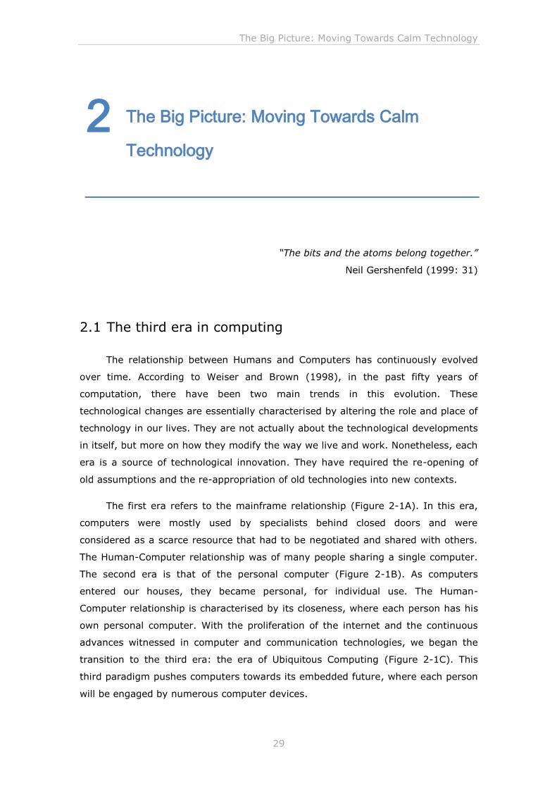
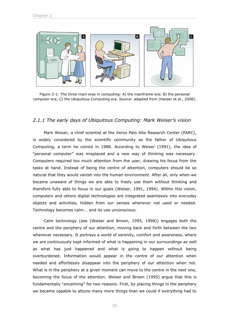
Figure 2-1: The three main eras in computing: A) the mainframe era; B) the
personal computer era; C) the Ubiquitous Computing era. Source: adapted from
(Harper et al., 2008). .................................................................................... 30
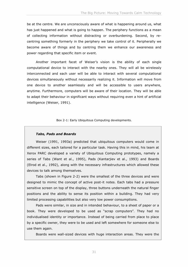
Figure 2-2: Picture of a Xerox PARC tab. Source: (Greenfield, 2006b). ................ 32
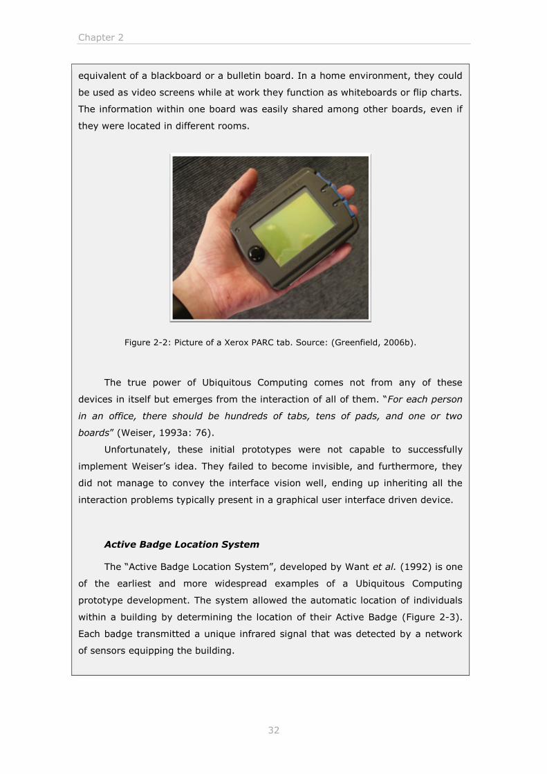
Figure 2-3: Picture of an Active Badge. Source: (AT&T Laboratories Cambridge,
2002). ......................................................................................................... 33
Figure 2-4: musicBottles installation. Source: (Ishii et al., 1999). ....................... 37
Figure 2-5: Overview of printing technologies. Source: adapted from (Kipphan,
2001). ......................................................................................................... 45
Figure 2-6: Schematic illustration of the flatbed screen printing (top) and rotary
screen printing (bottom) methods. Source: adapted from (Kipphan, 2001). ......... 48
Figure 2-7: Schematic illustration of the flexography printing process. Source:
Adapter from (Kipphan, 2001)........................................................................ 49
Figure 2-8: Schematic illustration of the lithography offset printing process. Source:
Adapter from (Kipphan, 2001)........................................................................ 50
Figure 2-9: Schematic illustration of the gravure printing process. Source: Adapter
from (Kipphan, 2001). .................................................................................. 52
Figure 2-10: Inkjet printing processes. Source: adapted from (Kipphan, 2001). ... 53
Figure 2-11: Schematic illustration of the functioning principle of continuous inkjet
printing: (a) binary deflection system, and (b) multiple deflection system. .......... 54
Figure 2-12: Schematic illustration of the functioning principle of drop-on-demand
inkjet printing: (a) thermal system, (b) piezo system, and (c) electrostatic system.
.................................................................................................................. 55
14
Figure 3-1: Examples of cave paintings. Source: (Clottes, 2002). ....................... 80
Figure 3-2: Example of an Egyptian illustrated manuscript (Papyrus of Hunefer).
Source: (Meggs and Purvis, 2011). ................................................................. 81
Figure 3-3: Non-emissive displays operation modes: a) transmissive, b) reflective,
and c) transflective. ...................................................................................... 84
Figure 3-4: Schematic configuration and operating principle of an electrochromic
display. ....................................................................................................... 86
Figure 3-5: Representation of a simple electrochromic display. Source: (Ynvisible,
2011). ......................................................................................................... 87
Figure 3-6: Schematic illustration of the principle behind electrophoretic display
technology. Source: Based on (Chen et al., 2003). ........................................... 90
Figure 3-7: Examples of commercially available applications of electrophoretic
displays. Source: (E Ink, 2012b, 2012c, 2012f). ............................................... 92
Figure 3-8: Picture of a full-colour quick-response liquid powder display. Source:
(Hattori et al., 2010). .................................................................................... 94
Figure 3-9: Schematic illustration of the principle behind electrowetting display
technology. Source: Based on (Feenstra et al., 2004). ...................................... 95
Figure 3-10: Picture of various electrowetting displays showing diverse colours.
Source: (Feenstra and Hayes, 2009). .............................................................. 96
Figure 3-11: Liquavista’s electrowetting display e-reader. Source: (Stevens, 2010).
.................................................................................................................. 97
Figure 3-12: Schematic illustration of the functioning principle behind an
interferometric modulation display. Source: Based on (Miles, 1997; Miles et al.,
2002). ......................................................................................................... 98
Figure 3-13: Picture of an interferometric modulation display e-reader fabricated by
Qualcomm. Source: (Qualcomm, 2013a). ........................................................ 99
Figure 3-14: Structure of a photonic crystals electrochemical cell showing the effect
of film thickness on reflected colours. Source: Based on (Graham-Rowe, 2007;
Opalux, 2013). ........................................................................................... 101
15
Figure 3-15: Different colour states of a P-Ink display. Source: (Opalux, 2013). . 101
Figure 3-16: Seven-segment P-Ink display demonstration. Source: (Heikenfeld et
al., 2011). ................................................................................................. 102
Figure 3-17: Schematic illustration of the operation principle of a leuco dye-based
thermochromic display. ............................................................................... 104
Figure 3-18: Thermochromic wallpaper activated by human touch. Source:
(Berzina, 2011). ......................................................................................... 105
Figure 3-19: Seven-Segment Thermochromic Display. Source: (Ramsey et al.,
2000). ....................................................................................................... 105
Figure 4-1: Assembly configuration of an electrochromic displays. .................... 116
Figure 4-2: Schematic representation of a drive circuit for a simple electrochromic
display controlled by a toggle button. ............................................................ 123
Figure 4-3: Illustration of a two-digit seven-segment display configuration ........ 124
Figure 4-4: Schematic representation of the configuration of a seven-segment
electrochromic display. ................................................................................ 125
Figure 4-5: Schematic representation of a seven-segment, direct addressing
electrochromic display drive circuit. .............................................................. 126
Figure 4-6: Examples of direct addressing electrochromic displays. ................... 127
Figure 4-7: Direct addressing 4x4 electrochromic matrix display. ..................... 129
Figure 4-8: Comparison between the layout of a seven-segment, direct addressing
arrangement and the layout of a passive-matrix arrangement. ......................... 130
Figure 4-9: Circuit diagram for a passive-matrix display. ................................. 130
Figure 4-10: Schematic representation of the configuration of a passive-matrix
electrochromic display. ................................................................................ 132
Figure 4-11: Schematic representation of a 4x4 passive-matrix electrochromic
display drive circuit. .................................................................................... 133
Figure 4-12: Pixel activation mechanism on a passive-matrix electrochromic
display. ..................................................................................................... 134
16
Figure 4-13: Example of a 4x4 passive-matrix electrochromic display. .............. 134
Figure 4-14: Circuit diagram for an active-matrix display................................. 137
Figure 4-15: Example of a 5x5 active-matrix electrochromic display. Source:
(Andersson et al., 2007). ............................................................................. 137
Figure 4-16: Schematic illustration of the column and row electrodes in a 2x2
active-matrix electrochromic display. Source: adapted from (Andersson et al.,
2007). ....................................................................................................... 138
Figure 4-17: Illustration of a simple two-frame animation (animation flows from
right to left). Source: adapted from (Thomas and Johnston, 1997). .................. 141
Figure 4-18: Example of a type I-A electrochromic display - Electrochromic
postcard. Source: (Ynvisible, 2012). ............................................................. 141
Figure 4-19: Example of a type I-B electrochromic display – Football player. ..... 142
Figure 4-20: Football player KeyFrame-based electrochromic display: (a) final
prototype and (b) electronic circuit. .............................................................. 143
Figure 4-21: Circuit diagram of the “Football Player” electrochromic display control
unit. ......................................................................................................... 143
Figure 4-22: Layout configuration of a a) seven-segment, b) fourteen-segment, and
c) sixteen-segment display. ......................................................................... 145
Figure 4-23: Example of a type II-A electrochromic display - Seven-segment
display. ..................................................................................................... 145
Figure 4-24: Another example of a type II-A electrochromic display – Digital dice.
................................................................................................................ 146
Figure 4-25: Digital dice electrochromic display: (a) final prototype and (b) view of
the electronic circuit.................................................................................... 147
Figure 4-26: Circuit diagram of the “Digital Dice” electrochromic display control
unit. ......................................................................................................... 147
Figure 4-27: Example of various pictograms. Source: (Uebele, 2007). .............. 148
17
Figure 4-28: Example of a type II-B, segment-based electrochromic display –
Waste reminder. ......................................................................................... 149
Figure 4-29: Municipal solid waste icons. From left to right: household waste, paper
and cardboard recycling, mixed plastic and metal recycling. ............................. 150
Figure 4-30: Circuit diagram of the “Waste Reminder” electrochromic display
control unit. ............................................................................................... 150
Figure 4-31: Example of a type II-B, matrix-based electrochromic display - Weather
station display. ........................................................................................... 151
Figure 4-32: Weather forecast icons. From left to right: sunny, cloudy, rainy, and
snowy. ...................................................................................................... 151
Figure 4-33: Illustration of a multi-character/pictographic segmented display. ... 152
Figure 4-34: Illustration of a 7x5 matrix configuration reproducing diverse
alphanumeric characters. ............................................................................ 153
Figure 4-35: Illustration of a 7x5 matrix configuration reproducing diverse
pictograms. ............................................................................................... 153
Figure 4-36: Example of a type III-B electrochromic display in which the pixels are
pictorial images representing a living organism. ............................................. 154
Figure 4-37: Mock-up example of a type III-B configuration for a pictorial
simulation environment (each square represents a pixel of the display). ............ 155
Figure 5-1: Comparison between examples of pigmentation patterns on mollusc
shells (top images) and the evolution of specific one-dimensional cellular
automaton rules (bottom images). Source: adapted from (Wolfram, 2002). ....... 160
Figure 5-2: Comparison between examples of typical snowflakes patterns (top
images) and the evolution of a two-dimensional cellular automaton that remarkably
reproduces the basic snowflake formation process (bottom images). Source:
adapted from (Wolfram, 2002). .................................................................... 161
Figure 5-3: Common spatial arrangements of cellular automata elements in a) one-
dimension, b) two-dimension, and c) three dimension lattices. ......................... 164
Figure 5-4: Example of commonly used cell tilling: a) square tilling, b) regular
hexagon tilling, and c) regular triangle tilling. ................................................ 165
18
Figure 5-5: Classical neighbourhood of two-dimension cellular automata: a) von
Neumann neighbourhood, b) Moore neighbourhood, and c) a combined Moore
neighbourhood with an extended von Neumann neighbourhood. ....................... 165
Figure 5-6: The Game of Life rules. ............................................................... 167
Figure 5-7: Example of common still lifes in the Game of Life. .......................... 168
Figure 5-8: Example of common oscillators in the Game of Life. ....................... 168
Figure 5-9: Example of a “spaceship” moving in the Game of Life. .................... 168
Figure 5-10: Exemplification of the pictorial simulation behaviour and interaction
Rules. ....................................................................................................... 172
Figure 5-11: Architecture of the pictorial simulation environment. .................... 173
Figure A-1: Spectra of iron hexacyanoferrate films on tin-doped indium oxide
(ITO)/glass at various voltage potentials. Source: (Mortimer, 2011). ................ 234
Figure A-2: The three common redox states of Viologens: a) dication, b) radical
cation, and c) neutral species. Source: adapted from (Mortimer et al., 2006). .... 236
Figure A-3: Chemical structures of various aromatic compounds that can undertake
chemical or electrochemical oxidation to produce conducting polymers. Source:
adapted from (Rowley and Mortimer, 2002). .................................................. 237
Figure A-4: PEDOT chemical structure. .......................................................... 240
Figure A-5: Spectroelectrochemistry for a PEDOT film on tin-doped indium oxide
(ITO). Source: (Mortimer, 2011). ................................................................. 240
Figure A-6: Chemical structure of PEDOT:PSS. Source: adapted from (Monk et al.,
2007). ....................................................................................................... 241
Figure A-7: Schematic representation of the three different types of structures of
metallopolymers. Source: adapted from (Wolf, 2001). .................................... 243
Figure C-1: Epilog Mini 24 - Legend Elite Series control panel. ......................... 251
Figure D-1: Graphical user interface of the control software used to interact with
direct addressing electrochromic displays. ..................................................... 253
19
Figure D-2: Source-code architecture of the control software developed for
operating direct addressing electrochromic displays. ....................................... 254
Figure E-1: Graphical user interface of the control software used to interact with
passive-matrix electrochromic displays. ......................................................... 255
Figure E-2: Source-code architecture of the control software developed for
operating passive-matrix electrochromic displays. .......................................... 256
Figure I-1: Source-code architecture of the multi-layer pictorial simulation system.
................................................................................................................ 264

20
21
List of Tables
Table 2-1: Comparison between Printed Electronics and conventional electronics. 40
Table 2-2: Comparison of printing technologies typically used in Printed Electronics.
.................................................................................................................. 46
Table 2-3: Conductivity and resistivity values, at 20 ºC, of functional elements
commonly used in the formulation of conductive inks. ....................................... 58
Table 3-1: Side-by-side comparison of different non-emissive display technologies
based on various performance factors. .......................................................... 108
Table 4-1: Commonly used electrochromic materials. ..................................... 118
Table 4-2: Electrochromic displays visual content formats. .............................. 140
Table 4-3: Common layouts for segmented displays. ...................................... 146
Table 5-1: Cellular automata basic classes of behaviour. ................................. 169
Table 5-2: List of pictorial transition rules. ..................................................... 171
Table A-1: Colour states of relevant electrochromic transition metal oxides. ...... 232
Table C-1: Epilog Mini 24 - Legend Elite Series cut and engraving parameters.... 251

22
- Blank Page -
Introduction
23
1 Introduction
“The most profound technologies are those that disappear.
They weave themselves into the fabric of everyday life
until they are indistinguishable from it.”
Mark Weiser (1991: 1)
1.1 The world is the next interface
If we carefully look around us, it is possible to perceive how computers1 have
become an integral part of our live. They have profoundly and irrevocably changed
the way we perform most of our daily tasks, including the way we work, shop,
bank, and communicate with our friends and relatives. Simple tasks such as writing
a letter, listening to music or reading the news have been utterly altered by
computers to a point where most of us cannot imagine realising them without the
aid of one. The continuous miniaturisation of microprocessors as well as of other
electronic components drove this reality. As computers became smaller, cheaper,
and more powerful, their number and presence in our daily life grew remarkably.
Moreover, we witness an almost explosive diversification in the nature of computer
devices. Nowadays, computers can take various forms and sizes, from smartphones
and tablet computers to the credit-card sized Raspberry Pi. Furthermore, they are
present and are a crucial component of numerous artefacts and devices such as
wristwatches, music players, televisions, washing machines, and microwave ovens.
It is foreseen that in a near future computers will not only be an integrant
part of every product we buy but they will in fact be embedded within us and into
our environment, inevitably occupying our physical world as natural elements (see
for instance, (Gershenfeld, 1999; Greenfield, 2006a; Harper et al., 2008; Norman,
1 The term “computer” is used here in its broad sense, referring likewise to Personal Computers (PCs) or
other simpler computers such as microcontrollers.
Chapter 1
24
1999; Weiser, 1991)). Indeed, computers will become part of the very fabric of our
lives.
The proliferation of computers into our physical world promises more than the
obvious availability of computing infrastructure anywhere, any time. Computers will
enhance our human capabilities and our environment, promoting a reality that is
more responsive to our needs and expressive to dynamic changes in its
environment. Moreover, it implies a new paradigm of user interaction. The essence
of this new paradigm lies in transforming computation, until now essentially focused
on point-and-click graphical interfaces, into a new type of user experience, where
everything is controlled by natural actions based on our daily activities. We will
then be in the presence of intelligent environments, where people do not interact
directly with computers but instead are engaged by computer devices of all sizes
and types, without necessarily being aware of it (Weiser, 1994, 1999). Computers
become not only truly pervasive but also effectively invisible and unobtrusive to the
user. Achieving this paradigm shift will require tremendous efforts and creativity
from researchers. Not only it will be necessary to develop innovative approaches to
link the physical and the digital worlds, but it will also be fundamental to transform
the way people perceive computers. Furthermore, new ways to provide and present
information will also have to be considered. After all, “The world is the next
interface” (Gershenfeld, 1999: 169).
1.2 What is wrong with the computer?
Computers are complex machines. Possibly the most complex machine
humankind has ever created. However, computers complexity is a misleading one.
It results drastically from being a general purpose machine. As Norman (1999)
strongly agues in his book “The Invisible Computer”, the biggest problem of today’s
computer is that it “tries to be all things to all people” (1999: 70).
We use computers to perform the most various tasks. However, this is not
necessarily a virtue. As much as the computer empowers us, it also enslaves us.
Not only have we become dependent on computers, as they have diminished the
control we have over our lives. They impose on us, forcing us to adapt our nature
to its terms, rules, and interfaces. Furthermore, computers require too much
attention from us. Beyond the constant need of our time and patience due to
constant updates and optimisations as well as hardware failures and error
messages, computers demand our total focus when using them. Instead of being
Introduction
25
the centre of attention, computers should be invisible and unobtrusive, part of our
human environment (Norman, 1999; Weiser, 1991, 1993b, 1994). Moreover, as
Gershenfeld (1999) points out, interaction should happen in the context that we,
rather the computer, find meaningful.
1.3 Objective: Invisible technology
Technology should enhance in an invisible and unobtrusive way not only our
competences and productivity but also our enjoyment of life. By moving to simpler,
task-oriented devices, whose interface reflects the difficulty of the task and not the
complexity of the underlying technology, it is possible to keep in sight with our
needs (Norman, 1999). This ideal implies the perfect integration between
computers and the human environment. Hence, instead of a fixed display, keyboard
and mouse, the objects around us become the means we use to interact both with
the physical and digital worlds. For instance, tables, walls and floors are
transformed into interactive surfaces capable of providing us with subtle visual
information about our surrounding, along with the means to act upon it. This
requires not only for smaller, cheaper and low power consumption computers but
also for equally convenient visual information solutions that can be harmoniously
integrated into our surroundings.
With the advent of Printed Electronics, new ways to link the physical and the
digital worlds became available. By combining common printing techniques, such as
offset printing, flexography or inkjet printing, with conductive inks, it became
possible not only to mass-produce extremely thin, flexible and cost effective
electronic circuits, but also to introduce electronic functionality in products where it
was previously unavailable. As so, we are already witnessing the breakthrough of a
completely new set of products where the electrical circuits and some circuit
component, such as thin film transistors or resistors, are printed directly in almost
any type of organic or inorganic substrates, and thereby becoming an integrating
part of the material itself (see (Bennett, 2012; Bliss, 2013; Digital Arts Staff,
2012)). The conjugation with electrochromic inks (for example) enabled, in its turn,
the possibility to print and embed displays in these objects and products (see for
instance, (Cal Poly, 2012; Ynvisible, 2012)). Moreover, Printed Electronics can
create new opportunities for Personal Fabrication by giving individuals the
possibility to engineer their own embedded digital devices. Instead of relying on
mass-market manufacturers and purchase something that someone else thought
they wanted, users can fabricate exactly what they want (see, (Anderson, 2012;
Chapter 1
26
Gershenfeld, 1999, 2005)). Indeed, Printed Electronics can play a major role in the
democratisation of innovation. According to Hippel (2005), users’ ability to innovate
new products and services has been improving radically and rapidly as a result of
the steadily improving quality of computer software and hardware, improved access
to easy-to-use tools and components, and access to richer libraries of modifiable
innovations. Nowadays, it is possible for any individual to easily acquire, at
reasonable prices, kits that offer basic electronic and mechanical building blocks.
Furthermore, physical product prototyping is becoming easier as computer driven
3D printers become more affordable and sophisticated. The idea of users using the
concepts behind Printed Electronics for Personal Fabrication has the potential to
empower them, by further enhancing their ability to shape the digital and physical
spheres according to their specific needs.
The overall objective of this research work is to further contribute to the
Ubiquitous Computing vision and the concept of calm technology by introducing and
exploring the use of Printed Electronics and Personal Fabrication technologies in this
context. In particular, it aims at the development of task-specific, interactive digital
devices capable of presenting dynamic visual information seamlessly integrated in
our daily objects and surrounding environment, whilst employing the minimal
hardware and software resources. To this aim the following research was carried
out to resolve some of the challenges that this vision poses:
1) Based on the foreseen potentials of Printed Electronics, focus was given to
it as the preferential approach in the creation of the various components
of the digital devices, and to the use of printed electrochromic displays as
the medium for delivering digital information. Starting from simple, fixed
image, electrochromic displays, it was researched how dynamic visual
content could be introduced in these particular type of displays. Direct
addressing (segmented) and matrix-addressing electrochromic display
were developed as well as the necessary hardware required to control
these devices. Various architectures and picture elements arrangements
were further explored and categorised based on their potential for
presenting dynamic visual information.
2) With the aim to make accessible the development of such devices to wider
audiences, including to the common individual, special attention was given
to the fabrication techniques, which intended to be as simple as possible
and based also on the principles behind Personal Fabrication.
Introduction
27
3) A pictorial computation model based on cellular automata principles is
later introduced as means to extend the visual potential of matrix-based
electrochromic displays. In particular, it is implied its use for creating
dynamic simulation models into electrochromic displays by means of
various pictorial entities. Envisaged applications include the modelling of
physical, chemical, biological, and environmental phenomena.
In sum, this research aims to pave the way towards the consolidation of the
Ubiquitous Computing vision via the integration of Printed Electronics technologies
whilst also pointing to the disruptive and empowerment potentials of Personal
Fabrication.
1.4 Roadmap
The remaining chapters of this document outline the motivation, core
concepts and building blocks to support this research as well as the main outcomes.
Chapter 2 presents the research rationale and literature review. It starts by
providing an historical overview of the vision of Ubiquitous Computing, highlighting
the core ideas and concepts behind it. An introduction to the topic of Printed
Electronics is followed. The main advantages, challenges and foreseen practical
applications are described and an extensive characterisation of the main printing
technologies currently used in this area is provided. The last section of this chapter
is dedicated to the topic of Personal Fabrication. It makes the connection between
the fields of Printed Electronics and Personal Fabrication, and how these can be
combined to enhance the state of the art of Ubiquitous Computing.
Chapter 3 explores the importance of visual information and discusses the
main non-emissive Printed Electronics display technologies available nowadays. It
explains the technology behind each type of display as well as their limitations.
Based on the outcome of the review of the various Printed Electronics display
technologies, electrochromic displays are pointed out as one of the most promising
technologies for the creation of simple, low cost, low power, digital devices capable
of providing dynamic visual information.
Chapter 4 represents the lion’s share of the research work. It addresses the
development of Printed Electronics devices specifically tailored for visual
information applications. The first section of this chapter is dedicated to the
development of an overall system architecture based on the use of direct
addressing (segmented) and matrix addressing electrochromic displays. The
various elements that compose an electrochromic display are described as well as
Chapter 1
28
the assembly process of the various devices. The second section, in turn, highlights
six main approaches for presenting visual information based on the architectures
developed, categorising them according with the capability to produce dynamic
content and animations.
Chapter 5 tackles how simple computation programmes such as cellular
automata can be a solution for creating complex visual patterns in the proposed
systems but as well as a means to perform computations with inherent temporal
and spatial dimensions. In particular, it is explored how pictorial entities can be
used in a computation model based on extended cellular automata principles to
programme dynamic simulation models into matrix-based electrochromic displays.
Finally, Chapter 6 states the conclusions of this work and makes suggestions
for future research.
The Big Picture: Moving Towards Calm Technology
29
2 The Big Picture: Moving Towards Calm
Technology
“The bits and the atoms belong together.”
Neil Gershenfeld (1999: 31)
2.1 The third era in computing
The relationship between Humans and Computers has continuously evolved
over time. According to Weiser and Brown (1998), in the past fifty years of
computation, there have been two main trends in this evolution. These
technological changes are essentially characterised by altering the role and place of
technology in our lives. They are not actually about the technological developments
in itself, but more on how they modify the way we live and work. Nonetheless, each
era is a source of technological innovation. They have required the re-opening of
old assumptions and the re-appropriation of old technologies into new contexts.
The first era refers to the mainframe relationship (Figure 2-1A). In this era,
computers were mostly used by specialists behind closed doors and were
considered as a scarce resource that had to be negotiated and shared with others.
The Human-Computer relationship was of many people sharing a single computer.
The second era is that of the personal computer (Figure 2-1B). As computers
entered our houses, they became personal, for individual use. The Human-
Computer relationship is characterised by its closeness, where each person has his
own personal computer. With the proliferation of the internet and the continuous
advances witnessed in computer and communication technologies, we began the
transition to the third era: the era of Ubiquitous Computing (Figure 2-1C). This
third paradigm pushes computers towards its embedded future, where each person
will be engaged by numerous computer devices.
Chapter 2
30
Figure 2-1: The three main eras in computing: A) the mainframe era; B) the personal
computer era; C) the Ubiquitous Computing era. Source: adapted from (Harper et al., 2008).
2.1.1 The early days of Ubiquitous Computing: Mark Weiser’s vision
Mark Weiser, a chief scientist at the Xerox Palo Alto Research Center (PARC),
is widely considered by the scientific community as the father of Ubiquitous
Computing, a term he coined in 1988. According to Weiser (1991), the idea of
“personal computer” was misplaced and a new way of thinking was necessary.
Computers required too much attention from the user, drawing his focus from the
tasks at hand. Instead of being the centre of attention, computers should be so
natural that they would vanish into the human environment. After all, only when we
became unaware of things we are able to freely use them without thinking and
therefore fully able to focus in our goals (Weiser, 1991, 1994). Within this vision,
computers and others digital technologies are integrated seamlessly into everyday
objects and activities, hidden from our senses whenever not used or needed.
Technology becomes calm... and its use unconscious.
Calm technology (see (Weiser and Brown, 1995, 1998)) engages both the
centre and the periphery of our attention, moving back and forth between the two
whenever necessary. It portrays a world of serenity, comfort and awareness, where
we are continuously kept informed of what is happening in our surroundings as well
as what has just happened and what is going to happen without being
overburdened. Information would appear in the centre of our attention when
needed and effortlessly disappear into the periphery of our attention when not.
What is in the periphery at a given moment can move to the centre in the next one,
becoming the focus of the attention. Weiser and Brown (1995) argue that this is
fundamentally “encalming” for two reasons. First, by placing things in the periphery
we became capable to attune many more things than we could if everything had to
The Big Picture: Moving Towards Calm Technology
31
be at the centre. We are unconsciously aware of what is happening around us, what
has just happened and what is going to happen. The periphery functions as a mean
of collecting information without distracting or overburdening. Second, by re-
centring something formerly in the periphery we take control of it. Peripherally we
become aware of things and by centring them we enhance our awareness and
power regarding that specific item or event.
Another important facet of Weiser’s vision is the ability of each single
computational device to interact with the nearby ones. They will all be wirelessly
interconnected and each user will be able to interact with several computational
devices simultaneously without necessarily realizing it. Information will move from
one device to another seamlessly and will be accessible to users anywhere,
anytime. Furthermore, computers will be aware of their location. They will be able
to adapt their behaviour in significant ways without requiring even a hint of artificial
intelligence (Weiser, 1991).
Box 2-1: Early Ubiquitous Computing developments.
Tabs, Pads and Boards
Weiser (1991, 1993a) predicted that ubiquitous computers would come in
different sizes, each tailored for a particular task. Having this in mind, his team at
Xerox PARC developed a variety of Ubiquitous Computing prototypes, namely a
series of Tabs (Want et al., 1995), Pads (Kantarjiev et al., 1993) and Boards
(Elrod et al., 1992), along with the necessary infrastructures which allowed these
devices to talk among themselves.
Tabs (shown in Figure 2-2) were the smallest of the three devices and were
designed to mimic the concept of active post-it notes. Each tabs had a pressure
sensitive screen on top of the display, three buttons underneath the natural finger
positions and the ability to sense its position within a building. They had very
limited processing capabilities but also very low power consumptions.
Pads were similar, in size and in intended behaviour, to a sheet of paper or a
book. They were developed to be used as “scrap computers”. They had no
individualised identity or importance. Instead of being carried from place to place
by a specific owner, they were to be used and left somewhere for someone else to
use them again.
Boards were wall-sized devices with huge interaction areas. They were the
Chapter 2
32
equivalent of a blackboard or a bulletin board. In a home environment, they could
be used as video screens while at work they function as whiteboards or flip charts.
The information within one board was easily shared among other boards, even if
they were located in different rooms.
Figure 2-2: Picture of a Xerox PARC tab. Source: (Greenfield, 2006b).
The true power of Ubiquitous Computing comes not from any of these
devices in itself but emerges from the interaction of all of them. “For each person
in an office, there should be hundreds of tabs, tens of pads, and one or two
boards” (Weiser, 1993a: 76).
Unfortunately, these initial prototypes were not capable to successfully
implement Weiser’s idea. They failed to become invisible, and furthermore, they
did not manage to convey the interface vision well, ending up inheriting all the
interaction problems typically present in a graphical user interface driven device.
Active Badge Location System
The “Active Badge Location System”, developed by Want et al. (1992) is one
of the earliest and more widespread examples of a Ubiquitous Computing
prototype development. The system allowed the automatic location of individuals
within a building by determining the location of their Active Badge (Figure 2-3).
Each badge transmitted a unique infrared signal that was detected by a network
of sensors equipping the building.
The Big Picture: Moving Towards Calm Technology
33
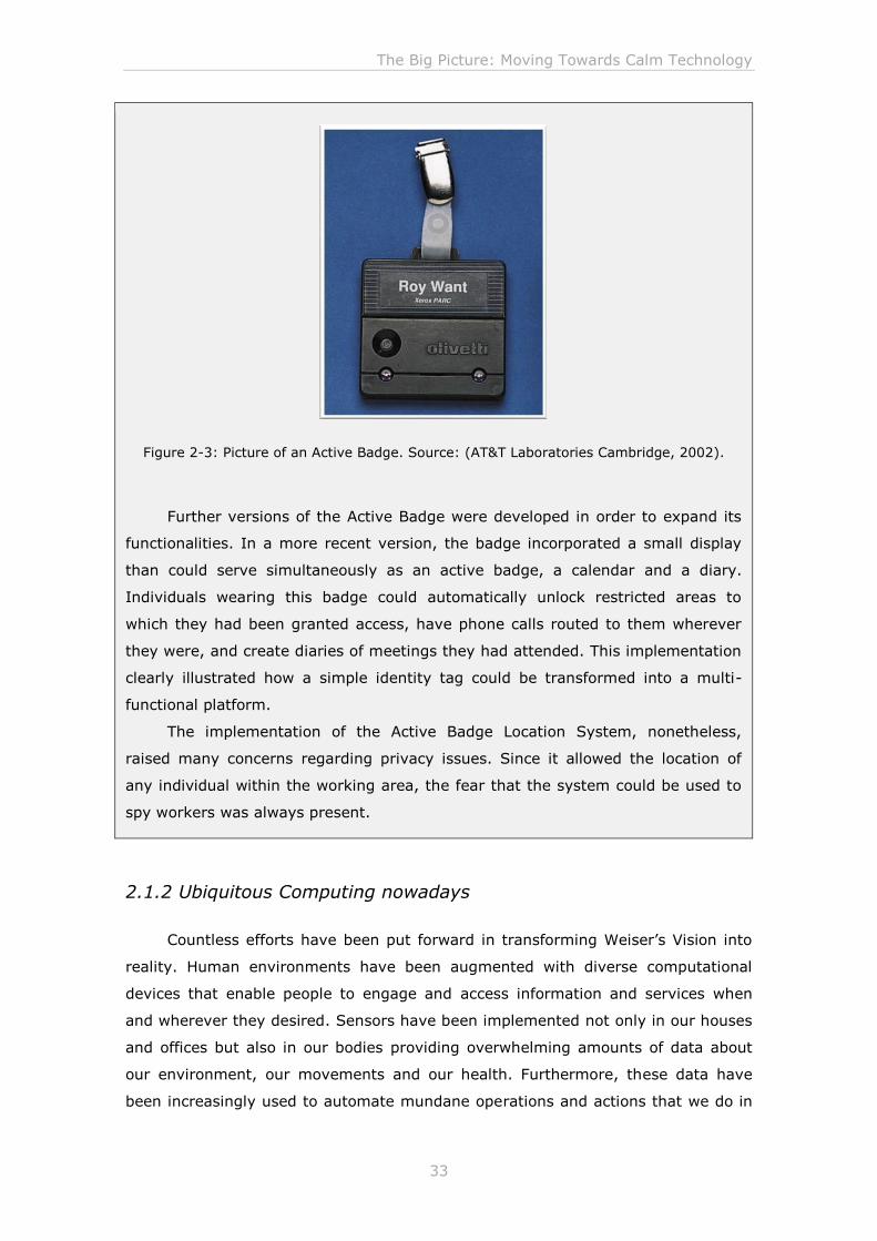
Figure 2-3: Picture of an Active Badge. Source: (AT&T Laboratories Cambridge, 2002).
Further versions of the Active Badge were developed in order to expand its
functionalities. In a more recent version, the badge incorporated a small display
than could serve simultaneously as an active badge, a calendar and a diary.
Individuals wearing this badge could automatically unlock restricted areas to
which they had been granted access, have phone calls routed to them wherever
they were, and create diaries of meetings they had attended. This implementation
clearly illustrated how a simple identity tag could be transformed into a multi-
functional platform.
The implementation of the Active Badge Location System, nonetheless,
raised many concerns regarding privacy issues. Since it allowed the location of
any individual within the working area, the fear that the system could be used to
spy workers was always present.
2.1.2 Ubiquitous Computing nowadays
Countless efforts have been put forward in transforming Weiser’s Vision into
reality. Human environments have been augmented with diverse computational
devices that enable people to engage and access information and services when
and wherever they desired. Sensors have been implemented not only in our houses
and offices but also in our bodies providing overwhelming amounts of data about
our environment, our movements and our health. Furthermore, these data have
been increasingly used to automate mundane operations and actions that we do in
Chapter 2
34
our daily life using conventional physical controls such as buttons and switches
(Rogers, 2006).
It is already possible to point out numerous devices that are clear indicators
of this new technological revolution. Mobile phones and smartphones with internet
capabilities, electronic labels and RFID (radio-frequency identification) tags,
miniature cameras and flexible displays, are just some examples of the
technologies currently available that are driving us towards the “post-PC era”. In
fact, devices such as the e-book reader and the tablet computer are roughly
overcoming the paradigm of the general-purpose personal computer in favour of
simple, specialised digital devices integrated in our life style. As Mattern (2004)
points out, the technological bases for a new world are already here.
It becomes also evident that the idea behind Ubiquitous Computing became
broaden. Weiser initial concept was further explored by other scholars (see for
instance, (Greenfield, 2006a; Mattern, 2001; Sakamura, 1996)) and rephrased to
incorporate new domains of application and novel concepts. The terms Pervasive
Computing, Mobile Computing and Ambient Intelligence became a synonym of
Ubiquitous Computing and expressions such as physical computing, smart devices,
tangible media or the Internet of Things are commonly used to describe the devices
involved to power these concepts (see (International Telecommunications Union,
2005; Mattern and Sturm, 2003; Ullmer and Ishii, 2001)). While a number of
authors defend that each concept is in its core different, others point out that the
differences between these terms is merely of academic nature. For example,
Lyytinen and Yoo (2002) argue that the concepts of Mobile Computing and
Pervasive Computing, despite being often used as synonyms of Ubiquitous
Computing, are conceptually different and employ different ideas of organising and
managing computing services. While Mobile Computing is fundamentally about
improving the capability to physically move computing services between
environments, Pervasive Computing refers to the capability that computers have to
obtain the information from the environment in which they are embedded and to
use that information to dynamically built computational models. Hence, the authors
present Ubiquitous Computing as the integration of large-scale Mobile Computing
with the Pervasive Computing functionality. Greenfield (2006a), on the other hand,
considers all these concepts facets of one coherent paradigm of interaction that he
prefers to calls “everyware”. He points out that there are many forms of Ubiquitous
Computing, and regardless of the different and valid distinctions between each
definition, they are all indistinguishable and meaningless from the user’s
perspective. Hence, to the user, they are all aspects of a single paradigm.
The Big Picture: Moving Towards Calm Technology
35
The multiple variations of concepts can be seen as a product of the natural
evolution of technology. As technology evolved, the new discoveries pushed the
limits of the existing definition. In order to accommodate the new knowledge and
expertise, the concept of Ubiquitous Computing, inevitably become broader. Jeon et
al. (2007) argue that the important thing is to redefine the different concepts as a
general notion that incorporates the basic ideas suggested by all of them. The
authors propose a taxonomy of properties from which the different kinds of
ubiquitous systems and applications can be described and compared. “In order to
understand Ubiquitous Computing environment, overall characteristics of Ubiquitous
Computing should be considered first” (Jeon et al., 2007: 1230).
Independently of the various uses given to the concept of Ubiquitous
Computing and of the different terminologies adopted, the following basic principles
are always present:
- Ubiquitous Computing devices are integrated seamless into everyday
objects, becoming invisible. Interaction becomes natural, unconscious.
- Ubiquitous Computing devices are linked by wireless networks, becoming
available anywhere, anytime.
- Ubiquitous Computing devices are able to communicate among them and
to adapt to variations in the surrounding environment.
However, Mark Weiser’s vision of Ubiquitous Computing was not primarily
about the idea of “anytime and anyplace” computing. In fact, when Weiser coined
the term Ubiquitous Computing, this notion was already employed in a variety of
contexts. Nonetheless, as Ishii (2004) points out, Ubiquitous Computing ended up
being used as a new label for an old idea. Weiser´s concept was misunderstood
and, as a consequence, usually misapplied (see Weiser comments in (Ishii, 2004)).
Weiser´s idea was centred on the context of interface design. It “was never just
about “making” computers ubiquitous. It was always […] about awakening
computation mediation into the environment” (Weiser in Ishii, 2004: 1310). As a
way to stress and reinforce the ambient interface aspect, Weiser introduces the
concept of Calm Technology. However, the term Ubiquitous Computing and its
misleading connotations were already too popular in the field of computer science.
The effect obtained in influencing and shifting the current research was minimal.
Ishii and Ullmer (1997) stimulated by Weiser vision of Calm Technology,
developed the concept of Tangible Bits. Like Weiser, they pursued the vision of
moving beyond the traditional point-and-click graphical interfaces, to one that
Chapter 2
36
disappears into everyday objects. They explored novel ways of re-applying
augmented physical objects commonly used in daily life with digital technology.
Their aim was to bridge the gap between the digital and the physical environment
by making digital information tangible.
Box 2-2: Examples of Calm Technology.
ambientROOM
The ambienteROOM (Ishii et al., 1998) is a personal interface environment
designed to engage both the centre and the periphery of the user attention. It
consisted of an office room where several areas of the space were augmented to
display and communicate information through subtle cues of sound, light, or
motion. In addition, graspable objects, such as bottles, were used as a mean to
control the ambient media. The ambienteROOM environment explored the
periphery of human perception in computational environments through the
implementation of novel interfaces that merged the digital and the physical
environments.
Bottles
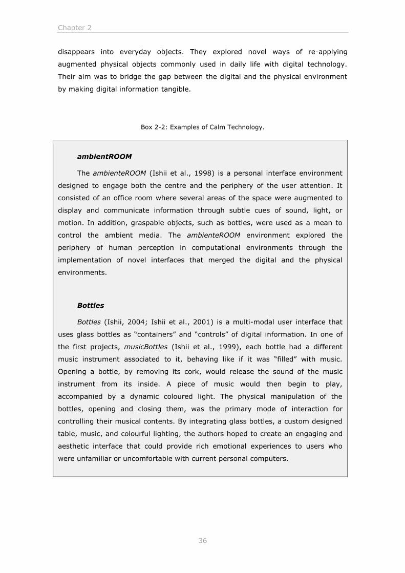
Bottles (Ishii, 2004; Ishii et al., 2001) is a multi-modal user interface that
uses glass bottles as “containers” and “controls” of digital information. In one of
the first projects, musicBottles (Ishii et al., 1999), each bottle had a different
music instrument associated to it, behaving like if it was “filled” with music.
Opening a bottle, by removing its cork, would release the sound of the music
instrument from its inside. A piece of music would then begin to play,
accompanied by a dynamic coloured light. The physical manipulation of the
bottles, opening and closing them, was the primary mode of interaction for
controlling their musical contents. By integrating glass bottles, a custom designed
table, music, and colourful lighting, the authors hoped to create an engaging and
aesthetic interface that could provide rich emotional experiences to users who
were unfamiliar or uncomfortable with current personal computers.
The Big Picture: Moving Towards Calm Technology
37
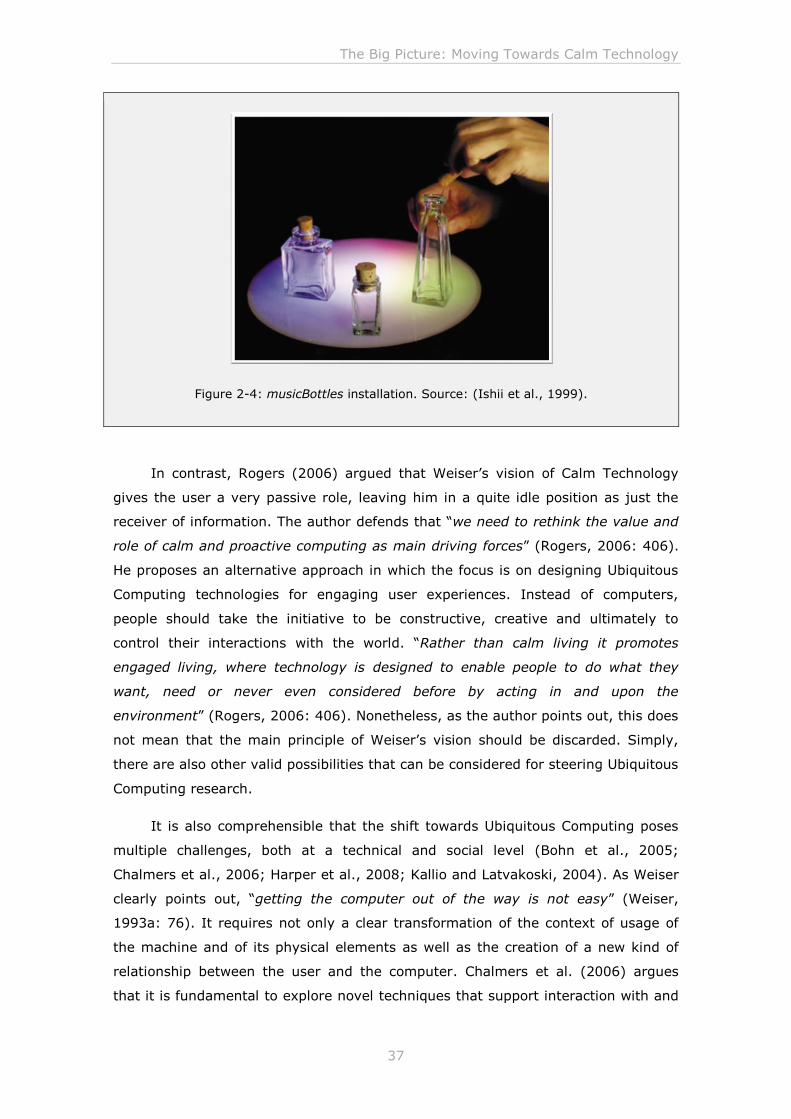
Figure 2-4: musicBottles installation. Source: (Ishii et al., 1999).
In contrast, Rogers (2006) argued that Weiser’s vision of Calm Technology
gives the user a very passive role, leaving him in a quite idle position as just the
receiver of information. The author defends that “we need to rethink the value and
role of calm and proactive computing as main driving forces” (Rogers, 2006: 406).
He proposes an alternative approach in which the focus is on designing Ubiquitous
Computing technologies for engaging user experiences. Instead of computers,
people should take the initiative to be constructive, creative and ultimately to
control their interactions with the world. “Rather than calm living it promotes
engaged living, where technology is designed to enable people to do what they
want, need or never even considered before by acting in and upon the
environment” (Rogers, 2006: 406). Nonetheless, as the author points out, this does
not mean that the main principle of Weiser’s vision should be discarded. Simply,
there are also other valid possibilities that can be considered for steering Ubiquitous
Computing research.
It is also comprehensible that the shift towards Ubiquitous Computing poses
multiple challenges, both at a technical and social level (Bohn et al., 2005;
Chalmers et al., 2006; Harper et al., 2008; Kallio and Latvakoski, 2004). As Weiser
clearly points out, “getting the computer out of the way is not easy” (Weiser,
1993a: 76). It requires not only a clear transformation of the context of usage of
the machine and of its physical elements as well as the creation of a new kind of
relationship between the user and the computer. Chalmers et al. (2006) argues
that it is fundamental to explore novel techniques that support interaction with and
Chapter 2
38
through new types of computational devices. Gesture-based approaches exploiting
movement in relation to surfaces and artefacts; haptic approaches exploiting the
physical manipulation of artefacts; and speech-based interfaces; need to be further
studied and developed. In addition, these solutions must fit the user’s needs, goals
and skills.
New ways to provide and present information, both visually and non-visually,
also need to be envisaged. Users must be able to easily access the information in a
comprehensive and clear way. Moreover, in order to effectively design systems that
can be perceived both in the periphery as well as in the centre of the attention, a
detailed understanding of not only how information can be presented but as well as
how it is perceived at the different levels of the human attention must be procured.
Naturally, it becomes also important to consider how these transitions between the
different levels of awareness can be eased and smoothed for the user experience
(Bakker et al., 2010; Brown and Duguid, 1996; Eggen and Mensvoort, 2009).
Understanding how users will interact and experience Ubiquitous Computing
technologies and how these can be integrated in human activities along with its
consequences, is fundamental for the creation of useful and suitable interfaces and
interactions. Ubiquitous Computing systems must be sufficiently simple and
transparent so that people can understand effortlessly how to interact with them.
Hence, it is necessary to develop all-inclusive standardised invisible interfaces. New
hardware components have to be assembled, new network protocols created and
software developed but also further studies have to be conducted to better
understand the interaction between Man and Machine. The social and cultural
realms also pose a great importance and must also be taken into consideration.
Always present are as well concerns about invasion of privacy; data and
consumer protection; trust, accountability and security of systems; and loss of
control (Friedewald and Raabe, 2011; Hayat et al., 2007; Want et al., 2002).
Naturally, users will want to take advantage of the Ubiquitous Computing potential
and be able to engage and be engaged by every object they encounter without
worrying about security and privacy issues. Success in addressing these challenges
will inevitably require the expansion of Ubiquitous Computing research to areas
outside computer science. Hence, as mentioned above, it becomes fundamental to
transpose the traditional barriers between the social and the technical realms and
promote the close collaboration between computer engineers and social theorists.
Indeed, given the potential changes that Ubiquitous Computing can bring to
business practices, commerce, governance, and overall everyday life, there is huge
potential for social science research.
The Big Picture: Moving Towards Calm Technology
39
2.2 The advent of Printed Electronics
When Johannes Gutenberg invented the movable type printing press around
1440, he initiated a revolution in the distribution of knowledge. His invention
allowed that individual letters and punctuation symbols could be used over and over
again to print the words and sentences in each page of a book, making it possible
to produce a large number of copies of a single work in a relatively short amount of
time, considering the previous alternative of manual copying. By the end of the
fifteenth century, hundreds of book titles were being produced each year on
wooden presses similar to the one developed by Gutenberg. This rapid spread of
knowledge made possible by Gutenberg's printing press ended up having a
fundamental role in the development of the Renaissance, the Protestant
Reformation and the Scientific Revolution (Gutenberg Museum Mainz, 2008; Harry
Ransom Center, 2007). In an analogous way, Printed Electronics intends to
revolutionise the production of digital devices by combining the achievements of the
printing industry and those of the electronics world. The term Printed Electronics
refers to the use of printing technologies to produce electronic circuits, components
and devices in a wide array of substrates, such as paper, plastic or textiles. Electro-
optical functional inks are used for this purpose, which are directly deposited on the
substrate, creating the various active and passive devices (e.g. transistors,
resistors, capacitors, antennas, and alike).
The interest in Printed Electronics lies primarily in the prospect that printing is
a low cost technique for the production of electronic systems, ultimately capable of
bringing down the manufacture cost of such products to values that conventional
silicon manufacturing cannot reach. The potential for cost savings comes from the
fact that Printed Electronics is based on the use of purely additive processing
methods, in contrast to the photolithography-based subtractive methods currently
used in the semiconductor industry (Subramanian et al., 2008). Not only is the
material only deposited where it is required, but also the overall complexity of the
manufacture process is greatly simplified. Typically, only two steps are required to
go from a bare substrate to a working functional layer on a substrate: the printing
process in itself and a curing process. If we consider that in subtractive methods
multiple steps, materials and equipments are necessary to produce a single
functional layer on a bare substrate, in addition to being consumed materials that
do not end up on the final device, the cost savings can be relatively high,
particularly when the device does not have a high surface coverage on the
Chapter 2
40
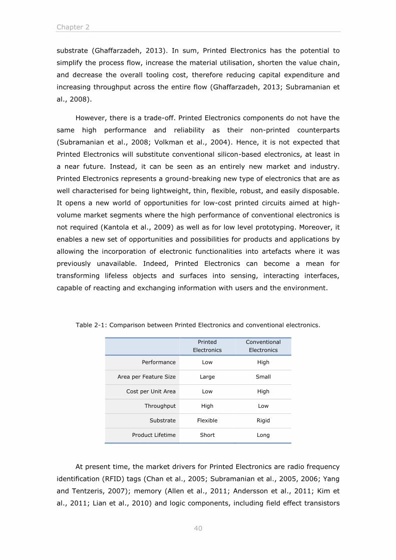
substrate (Ghaffarzadeh, 2013). In sum, Printed Electronics has the potential to
simplify the process flow, increase the material utilisation, shorten the value chain,
and decrease the overall tooling cost, therefore reducing capital expenditure and
increasing throughput across the entire flow (Ghaffarzadeh, 2013; Subramanian et
al., 2008).
However, there is a trade-off. Printed Electronics components do not have the
same high performance and reliability as their non-printed counterparts
(Subramanian et al., 2008; Volkman et al., 2004). Hence, it is not expected that
Printed Electronics will substitute conventional silicon-based electronics, at least in
a near future. Instead, it can be seen as an entirely new market and industry.
Printed Electronics represents a ground-breaking new type of electronics that are as
well characterised for being lightweight, thin, flexible, robust, and easily disposable.
It opens a new world of opportunities for low-cost printed circuits aimed at high-
volume market segments where the high performance of conventional electronics is
not required (Kantola et al., 2009) as well as for low level prototyping. Moreover, it
enables a new set of opportunities and possibilities for products and applications by
allowing the incorporation of electronic functionalities into artefacts where it was
previously unavailable. Indeed, Printed Electronics can become a mean for
transforming lifeless objects and surfaces into sensing, interacting interfaces,
capable of reacting and exchanging information with users and the environment.
Table 2-1: Comparison between Printed Electronics and conventional electronics.
Printed
Electronics
Conventional
Electronics
Performance Low High
Area per Feature Size Large Small
Cost per Unit Area Low High
Throughput High Low
Substrate Flexible Rigid
Product Lifetime Short Long
At present time, the market drivers for Printed Electronics are radio frequency
identification (RFID) tags (Chan et al., 2005; Subramanian et al., 2005, 2006; Yang
and Tentzeris, 2007); memory (Allen et al., 2011; Andersson et al., 2011; Kim et
al., 2011; Lian et al., 2010) and logic components, including field effect transistors
The Big Picture: Moving Towards Calm Technology
41
(FETs) (Ha rting et al., 2009; Schneider et al., 2008) and thin film transistors (TFTs)
(Burns et al., 2002; Kawase et al., 2003; D Kim et al., 2009); sensor arrays
(Harrey et al., 2002; Honeychurch and Hart, 2003; Laschi et al., 2006; Li et al.,
2007); photovoltaic cells (Barr et al., 2011; Krebs, 2009); batteries (Blue Spark,
2011; Enfucell, 2012; Hahn and Reichl, 1999; Hilder et al., 2009); and displays
(see section 3.2). The practical applications envisaged are various, and include, for
example:
- Dynamic newspapers, magazines, and signage applications: By taking
advantage of the combined benefits of paper with dynamic digital content,
companies can create novel formats to present visual information and
publicise their products. This will likely include the incorporation of
animated advertisements in magazines and newspapers, or the creation of
dynamic signage and billboards. Other possibilities include, but are not
limited to, posters, business cards, bumper stickers, and product packages
and labels.
- Intelligent packaging: Printed displays can be incorporated into products
packages not only with the aim of making them more visual appealing and
attractive, but also more useful and helpful. Hence, Printed Electronics
systems can be used in packaging to improving the legibility and detail of
the information available about the product, and thus improving the
information that consumers have access in the act of purchase, or can be
used to show notice messages about the conditions of the product,
highlighting changes that occurred in the surround environment and that
are incompatible with the preservation of the product. Furthermore, anti-
counterfeiting measures can also be implemented directly into the
products, preventing or at least complicating the falsification of products.
- Smart labels: From low-cost remotely updated electronic shelf labels and
pricing tags used in supermarkets and stores to dynamic information labels
for products.
- Smart cards: The implementation of Printed Electronics systems in smart
cards could allow users to rapidly access information contained in the card,
wherever and whenever they wanted. This would enable, for instance,
customers to easily check the amount of credits still remaining in a public
transportation smart card, or the validity of their subscription. Frequent
flyer card, or in any other type of loyalty system card could indicate the
fidelity points gathered, or alert the user for promotions. Healthcare smart
Chapter 2
42
cards could also be enhanced, allowing users to easily check certain
information on their medical file, such as the blood type, whether the
vaccines are up to date, when it was the last time he went to the doctor or
when he is supposed to have is next medical visit. Furthermore, Printed
Electronics solutions could also be used to improve the security of smart
cards, especially of debit and credit cards (e.g. by implementing digital
watermarks).
- Healthcare diagnostic devices: The disruptive potential of Printed
Electronics can be enormous in the healthcare sector. By enabling the
fabrication of disposable printed biosensors at a fraction of the cost of
equivalent non-printed solutions, they can make complex healthcare
examinations not only cheaper but also faster to do. These biosensors are
traditionally used in medical monitoring, diagnostics, and drug delivery.
Examples include biosensors for monitoring vital signs (e.g. heart rate,
body temperature, blood pressure); for testing metabolic variations (e.g.
blood glucose, cholesterol, lactate); and for detecting pathogens elements
(e.g. bacteria and virus).
- Energy harvesting and storage devices: Various printing technologies are
already being used as fabrication tools for manufacturing photovoltaic cells
and batteries. As printed photovoltaic cells become more efficient and more
reliable as a power source, they will eventually become more widespread.
Low-cost printed photovoltaic cells will allow energy to be generated where
it is needed. Considering their flexible nature, they can be easily integrated
into building structures, such as wall coverings, or made into window
shades. Likewise, printed batteries provide lightweight, flexible power
sources that can be integrated into mobile electronic devices, or in any
other type of low-power consumer application or Printed Electronic system.
- Dynamic walls and lighting panels: Printed Electronics systems can be
integrated into walls and be used as information screens or, alternatively,
as dynamic wallpapers or lighting panels.
- Active/smart clothing: Printed Electronics systems can also be integrated
seamlessly into textiles. They can be used to improve the functionality of
clothes, for instance, by using embedded biosensors and displays to
monitor and show the user vital signs, or instead, in a more fashionable
way, to simply display dynamic patterns in the fabric.
The Big Picture: Moving Towards Calm Technology
43
Naturally, the development of these applications is greatly conditioned by the
formulation of suitable functional inks as well as of adequate substrates where they
are printed (Kantola et al., 2009). After all, the practicality of Printed Electronics
relies primarily on the development of novel inks used to create the electronic
components. As for substrates used, so far the most common ones are polymer
films, ceramics, glass and silicon. Printing of functional inks on paper is also
possible, but can present some challenges due to the paper’s rough, fibrous surface
at a microscopic scale. The optimisation of current printing technologies for real
mass-manufacturing of Printed Electronic systems also has to be undertaken. As
Schmidt et al. (2006) points out, printing technologies were developed for visual
output and therefore classical printing products undergo completely different
requirements when compared to electronic devices. Significant modifications in
processes and materials are necessary.
For the purpose of this thesis, a digital device is regarded as an electronic
system that can receive, store, process and display digital information. It is
composed by the three simple interconnect modules: (1) the sensing module,
responsible for picking up the user inputs; (2) the computation module, responsible
for the data processing, transforming the inputs into relevant outputs; and (3) the
display module, responsible for outputting the results of the computation into a
human-readable form. A fourth module, the power module, can also be considered,
being responsible for supplying the necessary energy for the smooth operation of
the system.
2.2.1 Printing technologies
The assortment of printing technologies currently available for the production
of traditional printed products is relatively broad. Based on whether a master, i.e. a
printing plate or an image carrier from which the ink is transferred to the printing
substrate in order to reproduce text or images, is required or not, printed
technologies can be divided into conventional printing and non-impact printing,
respectively (Kipphan, 2001).
In conventional printing, the master is the medium responsible for carrying
the information during the printing process. As a result, information is generated on
the printing substrate based on the master layout, through direct contact and by
partial transfer of the printing ink. Each master corresponds to a single page of
information. In contrast, in non-impact printing, there is no master carrying
Chapter 2
44
permanent information, and text and images are produced without direct physical
contact between the printing mechanism and the printing substrate. Hence,
different information can be printed continuously on each page. The printing
process is based on digital information and, depending on the applied non-impact
printing technology the image is either transferred via an intermediate
carrier/imaging surface (e.g. electrophotography printing), or is transferred directly
without an intermediate carrier (e.g. inkjet printing). An overview of the various
printing technologies is provided in Figure 2-5.
Within the context of Printed Electronics, the most commonly used printing
technologies are screen, flexography, offset lithography, gravure, and inkjet.
Naturally, each process has its own strengths and limitations in regard to the
production of Printed Electronics. The choice of one process over another is typically
related to the type of ink, substrate used, and the final application intended (for
instance, prototyping versus high-precision). Hence, each process tends to be the
ideal method of production for a different range of products or substrates. In order
to fully take advantage of the production capabilities of conventional printing
technologies, their applicability in Printed Electronics should be target to roll-to-roll
processing (R2R). This essentially consists of adapting the printing technologies to
allow rotary printing. The process typically involves several rotating cylinders
around which the printing substrate is routed through a number of fabrication
operations. Hence, during the printing process, the substrate is on a constant move
and the imprint is done in a continuous process at impressively high speeds,
enabling large area capability, high throughput, and ultimately increasing the cost-
efficiency of the overall manufacture process.
In the following sub-sections, the most commonly used printing technologies
in Printed Electronics are described, highlighting their advantages and limitations.
Table 2-2 provides a comparative overview of these technologies.
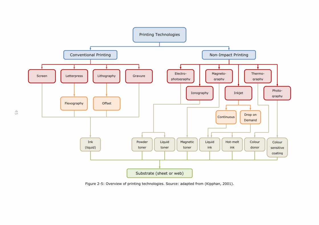
45
Figure 2-5: Overview of printing technologies. Source: adapted from (Kipphan, 2001).
Conventional Printing Non-Impact Printing
Screen
Letterpress
Lithography
Flexography
Gravure
Offset
Ionography
Magneto-
graphy
Inkjet Photo-
graphy
Thermo-
graphy
Electro-
photography
Ink
(liquid)
Continuous Drop on
Demand
Powder
toner
Liquid
toner
Magnetic
toner
Liquid
ink
Hot-melt
ink
Colour
donor
Colour
sensitive
coating
Substrate (sheet or web)
Printing Technologies
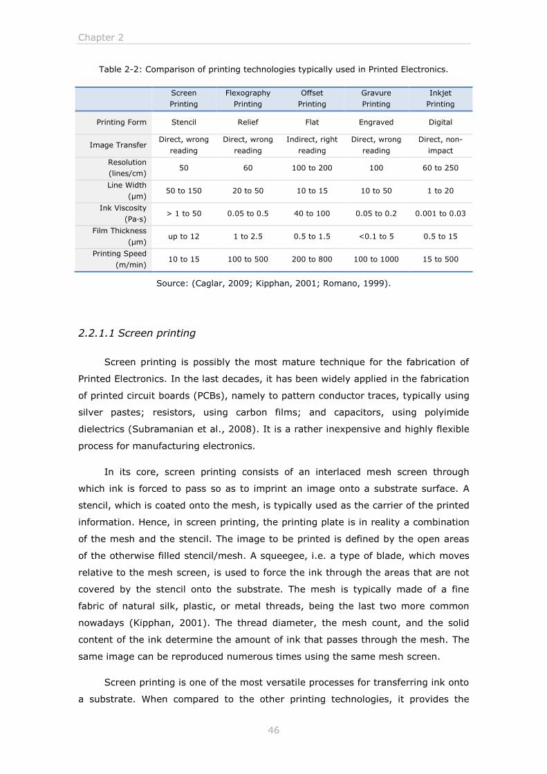
Chapter 2
46
Table 2-2: Comparison of printing technologies typically used in Printed Electronics.
Screen
Printing
Flexography
Printing
Offset
Printing
Gravure
Printing
Inkjet
Printing
Printing Form Stencil Relief Flat Engraved Digital
Image Transfer Direct, wrong
reading
Direct, wrong
reading
Indirect, right
reading
Direct, wrong
reading
Direct, non-
impact
Resolution
(lines/cm) 50 60 100 to 200 100 60 to 250
Line Width
(µm) 50 to 150 20 to 50 10 to 15 10 to 50 1 to 20
Ink Viscosity
(Pa·s) > 1 to 50 0.05 to 0.5 40 to 100 0.05 to 0.2 0.001 to 0.03
Film Thickness
(µm) up to 12 1 to 2.5 0.5 to 1.5 <0.1 to 5 0.5 to 15
Printing Speed
(m/min) 10 to 15 100 to 500 200 to 800 100 to 1000 15 to 500
Source: (Caglar, 2009; Kipphan, 2001; Romano, 1999).
2.2.1.1 Screen printing
Screen printing is possibly the most mature technique for the fabrication of
Printed Electronics. In the last decades, it has been widely applied in the fabrication
of printed circuit boards (PCBs), namely to pattern conductor traces, typically using
silver pastes; resistors, using carbon films; and capacitors, using polyimide
dielectrics (Subramanian et al., 2008). It is a rather inexpensive and highly flexible
process for manufacturing electronics.
In its core, screen printing consists of an interlaced mesh screen through
which ink is forced to pass so as to imprint an image onto a substrate surface. A
stencil, which is coated onto the mesh, is typically used as the carrier of the printed
information. Hence, in screen printing, the printing plate is in reality a combination
of the mesh and the stencil. The image to be printed is defined by the open areas
of the otherwise filled stencil/mesh. A squeegee, i.e. a type of blade, which moves
relative to the mesh screen, is used to force the ink through the areas that are not
covered by the stencil onto the substrate. The mesh is typically made of a fine
fabric of natural silk, plastic, or metal threads, being the last two more common
nowadays (Kipphan, 2001). The thread diameter, the mesh count, and the solid
content of the ink determine the amount of ink that passes through the mesh. The
same image can be reproduced numerous times using the same mesh screen.
Screen printing is one of the most versatile processes for transferring ink onto
a substrate. When compared to the other printing technologies, it provides the
The Big Picture: Moving Towards Calm Technology
47
widest range of application with regard to the choice of substrates. Apart from
paper and cardboard, other possible substrates are plastics, glass, metal, textiles,
ceramics, and the like, whether in the form of endless webs or single sheets.
Moreover, the substrate surface does not need to be planar, and thus objects of the
most varying shape can also be used as printing substrate. The range of suitable
inks is as well high. However, these need to have a paste-like behaviour. Screen
printing requires rather high viscosity inks, typically superior to 1000 cP (1 Pa·s),
with thixotropy2 properties. Inks with lower viscosities simply run through the mesh
and cause excessive spreading (Søndergaard et al., 2013; Subramanian et al.,
2008). It must be pointed nonetheless, that the use of high viscosity inks raises
some issues in the field of Printed Electronics. High viscosity inks are typically
manufactured by adding polymer binders to the ink, and these binders can destroy
the functionality of semiconductors, introduce excessive leakage and dissipation in
dielectrics, or degrade the conductivity of conductors (Subramanian et al., 2008).
Another characteristic of screen printing is that a greater thickness of ink (up to
12 µm) can be applied to the substrate than it is possible with any other printing
technique (Kipphan, 2001). This allows the patterning of very thick dry films, which
can be extremely useful for printed electrodes where high conductivity is needed.
In the context of Printed Electronics, screen printing has been widely used in
the production of polymer photovoltaic cells, to print both the front and back
electrodes as well as of complete cell modules (see for instance, (Aernouts et al.,
2004; Krebs, Gevorgyan, et al., 2009; Krebs, Jørgensen, et al., 2009; Shaheen et
al., 2001). Other examples include the production of displays, from electrochromic
displays (Brotherston et al., 1999; Coleman et al., 1999; Pettersson et al., 2002) to
organic light-emitting diode (OLED) displays (Birnstock et al., 2002; Jabbour et al.,
2001; Pardo et al., 2000) and field emission displays (FED) (Yukui et al., 2002;
Zeng et al., 2006); RFID antennas (Kim et al., 2012; Shin et al., 2009); and
various types of sensors (Hart and Wring, 1997; Hart et al., 2005; Honeychurch
and Hart, 2003; Laschi et al., 2006; Patel et al., 2001).
Figure 2-6 illustrates the traditional flatbed screen printing configuration and
the continuous rotary screen printing method.
2 Thixotropy consists of a reversible micro-structural change in the viscosity properties of a element
when submitted to shear stress. These elements are characterised by having a high viscosity at low
stress levels, but a decreased viscosity when an increased stress is applied (Barnes, 1997).
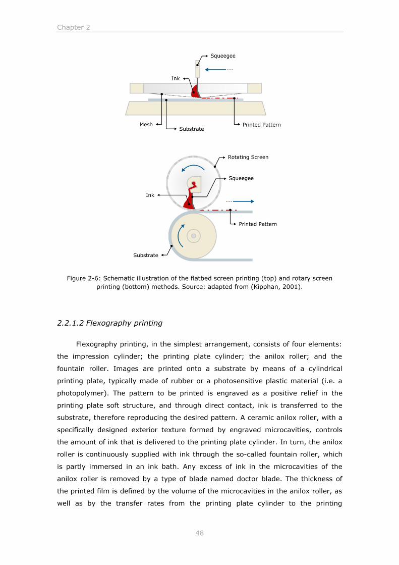
Chapter 2
48
Figure 2-6: Schematic illustration of the flatbed screen printing (top) and rotary screen
printing (bottom) methods. Source: adapted from (Kipphan, 2001).
2.2.1.2 Flexography printing
Flexography printing, in the simplest arrangement, consists of four elements:
the impression cylinder; the printing plate cylinder; the anilox roller; and the
fountain roller. Images are printed onto a substrate by means of a cylindrical
printing plate, typically made of rubber or a photosensitive plastic material (i.e. a
photopolymer). The pattern to be printed is engraved as a positive relief in the
printing plate soft structure, and through direct contact, ink is transferred to the
substrate, therefore reproducing the desired pattern. A ceramic anilox roller, with a
specifically designed exterior texture formed by engraved microcavities, controls
the amount of ink that is delivered to the printing plate cylinder. In turn, the anilox
roller is continuously supplied with ink through the so-called fountain roller, which
is partly immersed in an ink bath. Any excess of ink in the microcavities of the
anilox roller is removed by a type of blade named doctor blade. The thickness of
the printed film is defined by the volume of the microcavities in the anilox roller, as
well as by the transfer rates from the printing plate cylinder to the printing
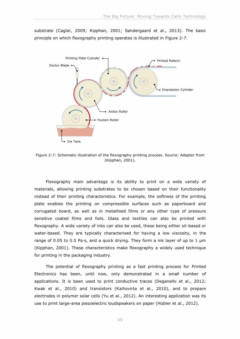
The Big Picture: Moving Towards Calm Technology
49
substrate (Caglar, 2009; Kipphan, 2001; Søndergaard et al., 2013). The basic
principle on which flexography printing operates is illustrated in Figure 2-7.
Figure 2-7: Schematic illustration of the flexography printing process. Source: Adapter from
(Kipphan, 2001).
Flexography main advantage is its ability to print on a wide variety of
materials, allowing printing substrates to be chosen based on their functionality
instead of their printing characteristics. For example, the softness of the printing
plate enables the printing on compressible surfaces such as paperboard and
corrugated board, as well as in metallised films or any other type of pressure
sensitive coated films and foils. Glass and textiles can also be printed with
flexography. A wide variety of inks can also be used, these being either oil-based or
water-based. They are typically characterised for having a low viscosity, in the
range of 0.05 to 0.5 Pa·s, and a quick drying. They form a ink layer of up to 1 µm
(Kipphan, 2001). These characteristics make flexography a widely used technique
for printing in the packaging industry.
The potential of flexography printing as a fast printing process for Printed
Electronics has been, until now, only demonstrated in a small number of
applications. It is been used to print conductive traces (Deganello et al., 2012;
Kwak et al., 2010) and transistors (Kaihovirta et al., 2010), and to prepare
electrodes in polymer solar cells (Yu et al., 2012). An interesting application was its
use to print large-area piezoelectric loudspeakers on paper (Hübler et al., 2012).
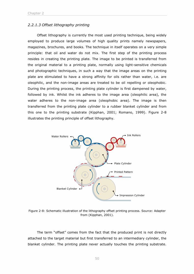
Chapter 2
50
2.2.1.3 Offset lithography printing
Offset lithography is currently the most used printing technique, being widely
employed to produce large volumes of high quality prints namely newspapers,
magazines, brochures, and books. The technique in itself operates on a very simple
principle: that oil and water do not mix. The first step of the printing process
resides in creating the printing plate. The image to be printed is transferred from
the original material to a printing plate, normally using light-sensitive chemicals
and photographic techniques, in such a way that the image areas on the printing
plate are stimulated to have a strong affinity for oils rather than water, i.e. are
oleophilic, and the non-image areas are treated to be oil repelling or oleophobic.
During the printing process, the printing plate cylinder is first dampened by water,
followed by ink. Whilst the ink adheres to the image area (oleophilic area), the
water adheres to the non-image area (oleophobic area). The image is then
transferred from the printing plate cylinder to a rubber blanket cylinder and from
this one to the printing substrate (Kipphan, 2001; Romano, 1999). Figure 2-8
illustrates the printing principle of offset lithography.
Figure 2-8: Schematic illustration of the lithography offset printing process. Source: Adapter
from (Kipphan, 2001).
The term “offset” comes from the fact that the produced print is not directly
attached to the target material but first transferred to an intermediary cylinder, the
blanket cylinder. The printing plate never actually touches the printing substrate.
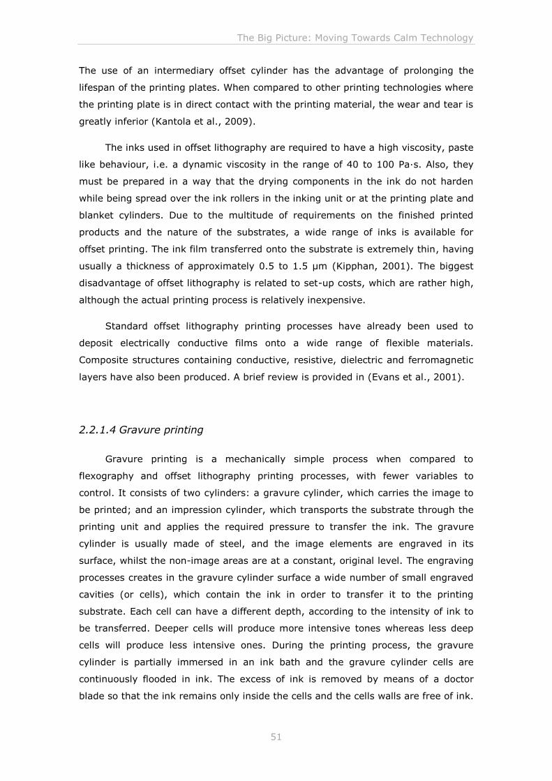
The Big Picture: Moving Towards Calm Technology
51
The use of an intermediary offset cylinder has the advantage of prolonging the
lifespan of the printing plates. When compared to other printing technologies where
the printing plate is in direct contact with the printing material, the wear and tear is
greatly inferior (Kantola et al., 2009).
The inks used in offset lithography are required to have a high viscosity, paste
like behaviour, i.e. a dynamic viscosity in the range of 40 to 100 Pa·s. Also, they
must be prepared in a way that the drying components in the ink do not harden
while being spread over the ink rollers in the inking unit or at the printing plate and
blanket cylinders. Due to the multitude of requirements on the finished printed
products and the nature of the substrates, a wide range of inks is available for
offset printing. The ink film transferred onto the substrate is extremely thin, having
usually a thickness of approximately 0.5 to 1.5 µm (Kipphan, 2001). The biggest
disadvantage of offset lithography is related to set-up costs, which are rather high,
although the actual printing process is relatively inexpensive.
Standard offset lithography printing processes have already been used to
deposit electrically conductive films onto a wide range of flexible materials.
Composite structures containing conductive, resistive, dielectric and ferromagnetic
layers have also been produced. A brief review is provided in (Evans et al., 2001).
2.2.1.4 Gravure printing
Gravure printing is a mechanically simple process when compared to
flexography and offset lithography printing processes, with fewer variables to
control. It consists of two cylinders: a gravure cylinder, which carries the image to
be printed; and an impression cylinder, which transports the substrate through the
printing unit and applies the required pressure to transfer the ink. The gravure
cylinder is usually made of steel, and the image elements are engraved in its
surface, whilst the non-image areas are at a constant, original level. The engraving
processes creates in the gravure cylinder surface a wide number of small engraved
cavities (or cells), which contain the ink in order to transfer it to the printing
substrate. Each cell can have a different depth, according to the intensity of ink to
be transferred. Deeper cells will produce more intensive tones whereas less deep
cells will produce less intensive ones. During the printing process, the gravure
cylinder is partially immersed in an ink bath and the gravure cylinder cells are
continuously flooded in ink. The excess of ink is removed by means of a doctor
blade so that the ink remains only inside the cells and the cells walls are free of ink.
Chapter 2
52
A more advanced ink filling method is achieved by using a chambered doctor blade
system, which can be advantageous for inks containing highly volatile solvents. The
ink is then transferred from the cells to the printing substrate by a high printing
pressure and the adhesive forces between the printing substrate and the ink. This
step requires a good contact between the printing substrate and the gravure
cylinder which can be ensured by using a soft impression cylinder (Kipphan, 2001;
Romano, 1999; Søndergaard et al., 2013). The functioning principle of gravure
printing is illustrated in Figure 2-9.
Figure 2-9: Schematic illustration of the gravure printing process. Source: Adapter from
(Kipphan, 2001).
Gravure printing is typically used to produce long run printings such as
magazines and newspaper inserts, catalogs, postage stamps, plastic laminates, and
packaging, since the surface of the gravure cylinder is plated with copper, which is
quite expensive (Romano, 1999). The inks used in gravure printing must have a
liquid behaviour, with a dynamic viscosity in the range of 0.05 to 0.2 Pa·s, so as to
fill the image forming cells of the gravure cylinder at high speeds (up to 15 m/s).
From a process point of view, these inks have a simple composition and
manufacture process. As a result, the range of workable inks is rather large.
Gravure printing also allows a wide range of printing thicknesses, from 50 nm to 5
µm (Kipphan, 2001).
In the context of Printed Electronics, the use of gravure printing for patterning
conductive traces has been widely reported (Pudas et al., 2004, 2005; Sung et al.,
2010), as well as being demonstrated its applicability, for example, in the
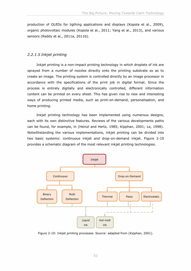
The Big Picture: Moving Towards Calm Technology
53
production of OLEDs for ligthing applications and displays (Kopola et al., 2009),
organic photovoltaic modules (Kopola et al., 2011; Yang et al., 2013), and various
sensors (Reddy et al., 2011a, 2011b).
2.2.1.5 Inkjet printing
Inkjet printing is a non-impact printing technology in which droplets of ink are
sprayed from a number of nozzles directly onto the printing substrate so as to
create an image. The printing system is controlled directly by an image processor in
accordance with the specifications of the print job in digital format. Since the
process is entirely digitally and electronically controlled, different information
content can be printed on every sheet. This has given rise to new and interesting
ways of producing printed media, such as print-on-demand, personalisation, and
home printing.
Inkjet printing technology has been implemented using numerous designs,
each with its own distinctive features. Reviews of the various developments paths
can be found, for example, in (Heinzl and Hertz, 1985; Kipphan, 2001; Le, 1998).
Notwithstanding the various implementations, inkjet printing can be divided into
two basic systems: continuous inkjet and drop-on-demand inkjet. Figure 2-10
provides a schematic diagram of the most relevant inkjet printing technologies.
Figure 2-10: Inkjet printing processes. Source: adapted from (Kipphan, 2001).
Binary
Deflection
Multi
Deflection
Thermal
Piezo
Electrostatic
Continuous
Liquid
ink
Hot-melt
ink
Drop-on-Demand
Inkjet
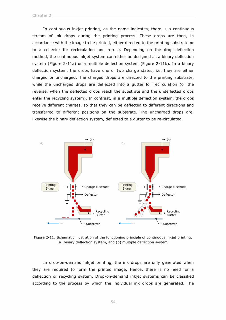
Chapter 2
54
In continuous inkjet printing, as the name indicates, there is a continuous
stream of ink drops during the printing process. These drops are then, in
accordance with the image to be printed, either directed to the printing substrate or
to a collector for recirculation and re-use. Depending on the drop deflection
method, the continuous inkjet system can either be designed as a binary deflection
system (Figure 2-11a) or a multiple deflection system (Figure 2-11b). In a binary
deflection system, the drops have one of two charge states, i.e. they are either
charged or uncharged. The charged drops are directed to the printing substrate,
while the uncharged drops are deflected into a gutter for recirculation (or the
reverse, when the deflected drops reach the substrate and the undeflected drops
enter the recycling system). In contrast, in a multiple deflection system, the drops
receive different charges, so that they can be deflected to different directions and
transferred to different positions on the substrate. The uncharged drops are,
likewise the binary deflection system, deflected to a gutter to be re-circulated.
Figure 2-11: Schematic illustration of the functioning principle of continuous inkjet printing:
(a) binary deflection system, and (b) multiple deflection system.
In drop-on-demand inkjet printing, the ink drops are only generated when
they are required to form the printed image. Hence, there is no need for a
deflection or recycling system. Drop-on-demand inkjet systems can be classified
according to the process by which the individual ink drops are generated. The
a) b)
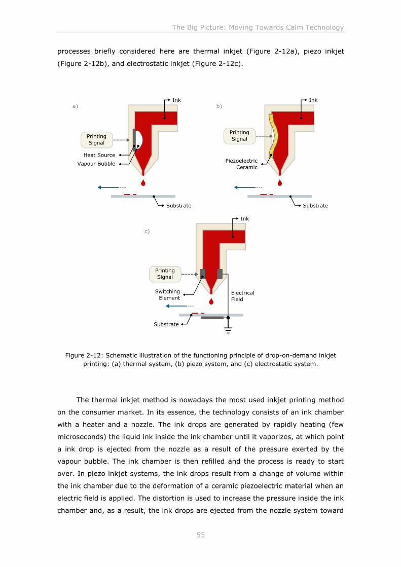
The Big Picture: Moving Towards Calm Technology
55
processes briefly considered here are thermal inkjet (Figure 2-12a), piezo inkjet
(Figure 2-12b), and electrostatic inkjet (Figure 2-12c).
Figure 2-12: Schematic illustration of the functioning principle of drop-on-demand inkjet
printing: (a) thermal system, (b) piezo system, and (c) electrostatic system.
The thermal inkjet method is nowadays the most used inkjet printing method
on the consumer market. In its essence, the technology consists of an ink chamber
with a heater and a nozzle. The ink drops are generated by rapidly heating (few
microseconds) the liquid ink inside the ink chamber until it vaporizes, at which point
a ink drop is ejected from the nozzle as a result of the pressure exerted by the
vapour bubble. The ink chamber is then refilled and the process is ready to start
over. In piezo inkjet systems, the ink drops result from a change of volume within
the ink chamber due to the deformation of a ceramic piezoelectric material when an
electric field is applied. The distortion is used to increase the pressure inside the ink
chamber and, as a result, the ink drops are ejected from the nozzle system toward
a) b)
c)
Chapter 2
56
the printing substrate. Electrostatic inkjet in turn, is based on the fact that an
electrical field exists between the inkjet system and the surface to be printed, and
that by means of image-dependent alterations in the inkjet nozzle system, either
the forces can be balanced or the surface tension ratios between the ink and the
outlet nozzle can be changed, so that a drop of ink is released as a result of the
field forces (Kipphan, 2001; Le, 1998).
One of the most crucial elements in an inkjet printing system, independently
of the method considered, is the printing nozzle. Each inkjet system is commonly
composed of thousands of high-precision nozzles, typically about 10 micrometers in
diameter. The characteristics of the ink drops, i.e. their volume, velocity, and
trajectory angle, are directly affected by the nozzle geometry. Even small
modifications in the manufacturing process of a nozzle can significantly alter the
printing quality. Hence, in order to achieve consistently uniform ink drops, the
diameter of each nozzle is fabricated with sub-micrometer accuracy. High resolution
printings require small ink drops volume and, as such, the nozzle diameter of print
heads has to be relatively small (Hanson, 2009; Le, 1998).
Inkjet technologies typically function with liquid inks with low viscosity (0.001
to 0.03 Pa·s), although piezo and electrostatic inkjet systems can also employ the
so called hot-melt inks. If liquid inks are used, the drying process occurs through
evaporation and absorption, which can be accelerated through the application of
heat. The use of hot-melt ink implies that the drying process is automatically
included in the printing process: hot-melt inks must be melted before printing and
quickly cool down and solidify upon printing, when in contact with the printing
substrate, due to being exposed to ambient temperature. The ink used and its
relation with the printing substrate determine the thickness of the ink layer and the
quality of the printed image. When liquid inks are used, very thin ink films can be
applied, resulting in thickness of approximately 0.5 µm. In the case of being used
hot-melt ink, the ink layer thickness ranges between 10 to 15 µm. Both types of ink
can comprise dyes or pigments as colorants (Kipphan, 2001; Romano, 1999).
The biggest advantages of inkjet printing, when compared to conventional
printing processes, are the possibility to easily change and adjust the printed
pattern on a computer without the need to manufacture a physical printing form,
and the ability to produce high quality prints, in a variety of substrates, at a
relatively low cost. The equipment is also cheaper and more compact, with the
added value that multiple print heads can be implemented and used during
printing. However, the productivity of these systems is still lower than conventional
The Big Picture: Moving Towards Calm Technology
57
printing technologies. Inkjet printing is a relatively new technology and presents
some limitation with respect to processing speeds and ink formulation.
Noteworthy about inkjet printing is that it allowed the democratisation of
printing by enabling desktop printing. Today, inkjet printers are practically within
the reach of everyone, being present in most households of the more economically
developed countries.
The use of inkjet printing in Printed Electronics is extensive, being reported its
applicability in most, if not all, of the applications described previously, from printed
memories (Allen et al., 2011) and transistors (Kawase et al., 2003; D Kim et al.,
2009), to displays (Chang et al., 1999; Furusawa et al., 2002; Shim et al., 2008;
Shimoda, 2003; Shimoda et al., 2003) and photovoltaic cells (Eom et al., 2009;
Galagan et al., 2012), including as well RFID modules (Yang and Tentzeris, 2007)
and sensors (Lee et al., 2005; Li et al., 2007).
2.2.2 Functional inks
Modern printing inks are commonly formed by four basic components: (1) the
colorant, usually a pigment although dyes can also be used, is responsible for
conferring the colour to the ink; (2) the binder, whose main purpose is to join the
various components of the ink together into a printable film and enable the ink to
attach onto the printing substrate; (3) the solvent, used to dissolve the binder and
make the ink flow so that it can be transferred to the printing surface; and (4) the
additive(s), which is added to manipulate the physical properties of the ink in order
to tune it to different situations. In a similar way, functional inks formulations are
composed by the same components, with the difference that the colorant element
found in printing inks is replaced by a functional element. It is this element that
confers the electro-optical properties to the functional ink. The proper formulation
of a functional ink involves a complex balance between all these elements. The ink
must provide a print film with an adequate cohesion and adhesion to the printing
substrate, in addition to possessing the electro-optical characteristics of the
functional element. One of the main challenges resides in fact in selecting the
adequate additives to improve the printability and processability of the ink without
interfering with the electro-optical characteristics of the ink, and thus the key
functionality of the printed object. Viscosity, surface tension, and wettability are all
critical characteristics in the formulation of conductive inks. The choice of an
adequate substrate can also greatly influence the performance of the functional ink.
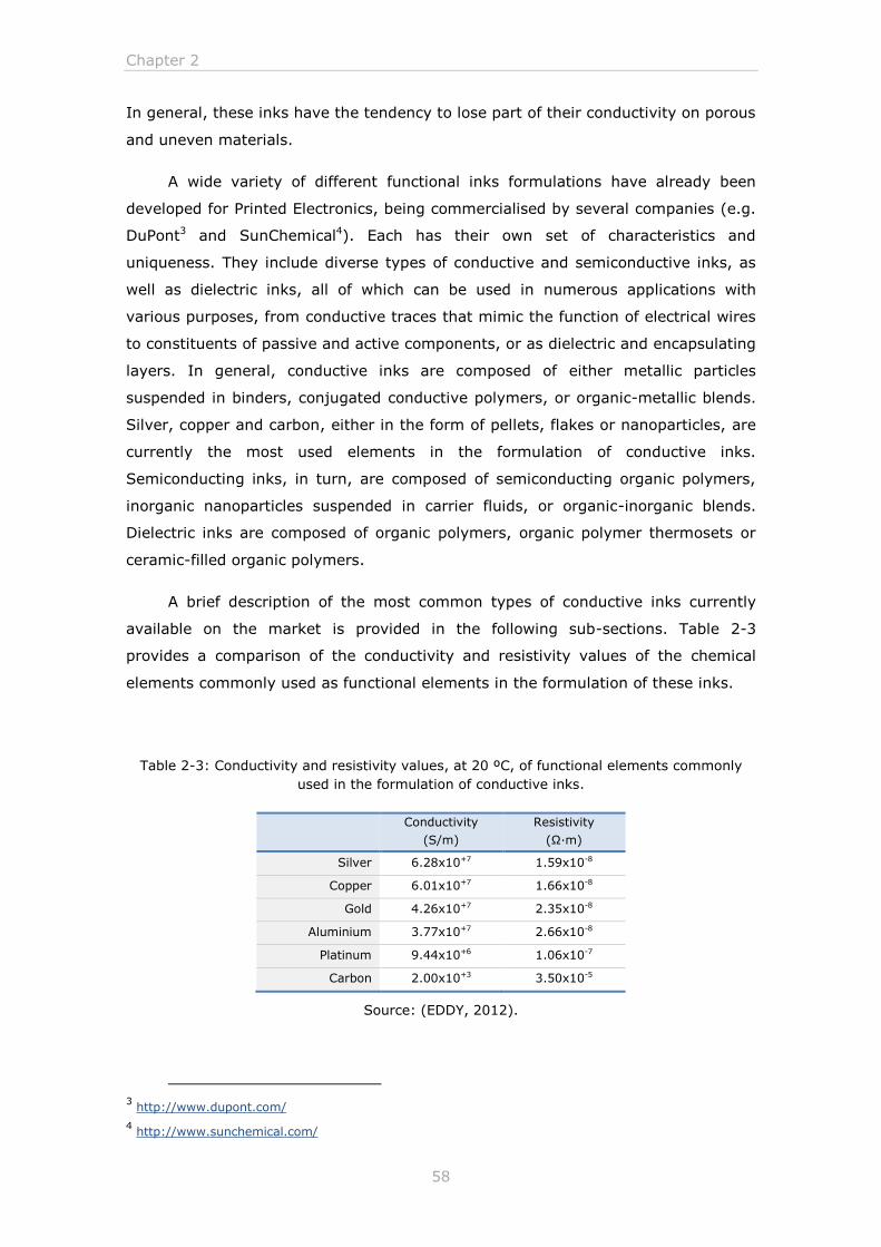
Chapter 2
58
In general, these inks have the tendency to lose part of their conductivity on porous
and uneven materials.
A wide variety of different functional inks formulations have already been
developed for Printed Electronics, being commercialised by several companies (e.g.
DuPont3 and SunChemical4). Each has their own set of characteristics and
uniqueness. They include diverse types of conductive and semiconductive inks, as
well as dielectric inks, all of which can be used in numerous applications with
various purposes, from conductive traces that mimic the function of electrical wires
to constituents of passive and active components, or as dielectric and encapsulating
layers. In general, conductive inks are composed of either metallic particles
suspended in binders, conjugated conductive polymers, or organic-metallic blends.
Silver, copper and carbon, either in the form of pellets, flakes or nanoparticles, are
currently the most used elements in the formulation of conductive inks.
Semiconducting inks, in turn, are composed of semiconducting organic polymers,
inorganic nanoparticles suspended in carrier fluids, or organic-inorganic blends.
Dielectric inks are composed of organic polymers, organic polymer thermosets or
ceramic-filled organic polymers.
A brief description of the most common types of conductive inks currently
available on the market is provided in the following sub-sections. Table 2-3
provides a comparison of the conductivity and resistivity values of the chemical
elements commonly used as functional elements in the formulation of these inks.
Table 2-3: Conductivity and resistivity values, at 20 ºC, of functional elements commonly
used in the formulation of conductive inks.
Conductivity
(S/m)
Resistivity
(Ω·m)
Silver 6.28x10+7 1.59x10⁻⁸
Copper 6.01x10+7 1.66x10⁻⁸
Gold 4.26x10+7 2.35x10⁻⁸
Aluminium 3.77x10+7 2.66x10⁻⁸
Platinum 9.44x10+6 1.06x10⁻⁷
Carbon 2.00x10+3 3.50x10⁻⁵
Source: (EDDY, 2012).
3 http://www.dupont.com/
4 http://www.sunchemical.com/
The Big Picture: Moving Towards Calm Technology
59
2.2.2.1 Silver-based and nanosilver inks
Silver-based inks are highly conductive and offer excellent flexibility. Indeed,
silver is the most conductive metal, with a conductivity of 6.28x10+7 S/m and a
resistance of 1.59x10⁻⁸ Ω·m at 20 ºC. Beyond the high conductivity, silver also
performs better than most metals under oxidative conditions (the oxide layer that is
formed during the cure process is conductive), possessing an excellent durability
under various conditions. Moreover, silver-based inks present a high mechanical
adherence to various substrates, making them ideal for use in a wide range of
electronic products, from sensors, flexible displays, photovoltaic cells, and RFID
antennas.
Silver-based inks are mostly sold under the form of silver flake inks, though
nanoparticles silver-based inks are gaining market share principally due to the fact
that flakes tend to be unsuitable for inkjet printing. They are too big for the printer
nozzles, frequently clogging them. While flake inks have particle diameters in the
range of microns, approximately from 0.5 to 8 µm, nanoparticles inks have nominal
particle diameters in the range of 2 to 50 nm (Laakso et al., 2009).
The sintering5 temperature of nano-sized metal particles is also lower when
compared to that of the counterpart metal in the bulk form (Buffat and Borel, 1976;
Qi, 2005). Typical sintering temperatures of 100 to 300 °C are required to burn-off
the organic additives present in nanoparticles inks and stimulate the sintering
process to realise a more densely packed silver layer and form a conductive film of
low resistance (Kim and Moon, 2005; Perelaer et al., 2008). The sintering time,
naturally, varies according with the composition of the ink used, though, typically, it
is only necessary a short period, in the order of 10 minutes. As the printed patterns
are heated above the temperature at which the particles lose their organic shell and
start showing conductance by direct physical contact, their resistance rapidly
decreases. However, conductivities values close to that of bulk silver are usually
only reached after sintering the printed patterns at temperatures above 200 to 250
ºC, sometimes as high as 400 ºC (Kamyshny et al., 2011). Obviously, this can end
up limiting the choice of substrate. For example, in order for the silver ink to be
compatible with plastic substrates the sintering must occur at a temperature lower
than 160 ºC (Li et al., 2005). Good film conductivities can, nonetheless, be
obtained at temperatures of this order. Dearden et al. (2005) reports the
formulation of silver-based inks with good conductivity values (2 to 3 times the
5 Sintering is a process, typically thermal, for bonding particles together into a coherent, predominantly
solid structure via mass transport events that occur fundamentally at atomic level (German, 1996).
Chapter 2
60
theoretical resistivity of bulk silver) at the relatively low temperature of 150 ºC. In
turn, Perelaer et al. (2008) demonstrated that silver-based inks containing very low
amount of organic additives revealed measurable conductivity already after
sintering at 80 ºC. Hence, it is of utmost importance to identify an optimum
between sintering time and temperature, and the obtained conductivity.
The methods for preparing metal nanoparticles, including silver and gold
nanoparticles to be used in conductive inkjet inks, can be divided into two main
strategies: (1) top-down and (2) bottom-up. Top-down, or physical methods are
generally high-energy methods, in which the bulk metal or the microscopic particles
are converted to nano-sized particles. These methods are expensive, energy-
consuming, and require sophisticated equipment. In bottom-up methods, in
contrast, nanoparticles are built up from metal atoms and nuclei, which are formed
either from precursor ions and molecules with the use of a proper reducing agent,
or from precursor molecules by their decomposition. Bottom-up preparation of
metal nanoparticles is usually performed in a liquid medium, which can vary from
water to polar and non-polar organic solvents and ionic liquids (Kamyshny et al.,
2011).
The biggest drawback of using silver-based inks is undoubtedly its cost. Silver
has a high price, making it expensive for many applications. Also, its price is very
susceptible to rate fluctuations, making it hard to estimate production costs.
Nonetheless, for now, silver is the most common precious metal used in the
development of conductive inks for Printed Electronics, existing a wide range of inks
formulations compatible with the printing processes addressed in this chapter. Its
high performance makes it a cost effective material that it is not easily replaced.
2.2.2.2 Copper-based and nanocopper inks
Copper-based inks present a conductivity roughly compared to that of silver-
based inks but at a more affordable price. Furthermore, likewise silver-base inks,
copper-based inks have a strong adhesion to a wide variety of substrate materials,
making them also suitable for printing electrical circuits in a broad range of
electronic products. The drawback is that copper is easily oxidised and, unlike the
silver oxide, the copper oxide is insulating. As a result, copper becomes less
conductive as it oxidises. Hence, protective agents capable to retard the oxidation
process are of utterly importance in the formulation of these inks. Moreover, it is
The Big Picture: Moving Towards Calm Technology
61
advisable that printed copper patterns be protected by an overcoat in order to
prevent the long term oxidation of the copper metal to copper oxide.
Printed copper patterns exhibited metal-like appearance and, as they dry
become more conductive. Sintering greatly improves the conductivity of these as it
speeds up the drying process and prevents the initial development of the copper
oxide layer that is typically formed during the drying process. High conductivity
values close to that of the bulk material require sintering at temperatures in the
order of 350 ºC (Haque et al., 2013; Park et al., 2007). However, good sintered
copper structures can be achieved at temperatures of 250 ºC (Lee et al., 2009).
Akin to silver-based inks, the use of temperatures lower than 160 °C allow the
application of copper-based inks to plastic substrates. Naturally, a compromise
must be achieved in terms of conductivity.
2.2.2.3 Gold-based and nanogold inks
Gold possesses a high conductivity (4.26x10+7 S/m at 20 ºC), only slightly
inferior to that of silver and copper, coupled with the added value of having a high
stability. Indeed, gold is one of the most non-reactive metals, only surpassed by
platinum, being unaltered by factors like heat and humidity. It has a general
resistance to oxidation and corrosion, never reacting with oxygen. Hence, it never
degrades, rusts or tarnishes over time. It is these characteristics, together with
gold’s unparalleled ductility and malleability that make it an essential element in
the field of electronics. It has a high work function and serves as the single most
reliable metal in the field.
The single and biggest drawback of gold is its high cost. If silver prices are
already considered high, with various efforts underway to identify more cost
effective alternatives such as copper-based inks, gold cost are even higher and
equally prone to market fluctuations. Nonetheless, there are several market
opportunities for gold-based inks, where the benefits of using gold can potentially
outweigh the higher cost. These include, for instance, the development of sensors
for environmental and medical applications (Bonfil et al., 2000; Laschi et al., 2006).
Chapter 2
62
2.2.2.4 Aluminium-based inks
Aluminium has a conductivity of 3.77x10+7 S/m, being alongside with silver,
copper, and gold as one of the best conductors known to date. It is the most
abundant metal on Earth and has an excellent resistance to corrosion. However,
this resistance results from a thin surface layer of aluminium oxide that is rapidly
formed when the metal is exposed to oxygen, which creates a physical barrier to
corrosion and further oxidation. The problem is that the aluminium oxide layer is
non-conductive, and thus greatly tampers the conductivity of aluminium-based
inks. Hence, like copper-based inks, aluminium-based inks require an overcoat
after application. On the positive side, aluminium is cheaper than copper.
Aluminium has been widely employed, under the form of thin foils, in the
manufacture of RFID antennas of so-called traditional RFID tags through
conventional printed circuit subtractive processes. However, under the context of
Printed Electronics, aluminium-based inks seem to be deprived in favour of silver
and copper-based inks. The low cost of aluminium-based inks appears to not justify
its use considering the performance lost. A report from the VTT Technical Research
Centre of Finland details the development of a low work function aluminium-based
ink, along with its advantages, that intends to be a substitute for printable silver
inks and pastes in a wide range of printed electronics applications. According to the
authors, it is ideal for organic photovoltaic and OLED display components, organic
field-effect transistors (OFET), RFID antennas, and sensor applications (Rupprecht
et al., 2012).
2.2.2.5 Platinum-based inks
Like gold and silver, platinum is a noble metal. It has a conductivity of
9.44x10+6 S/m and it is the least reactive metal on the periodic table of elements.
Hence, platinum exhibits an excellent resistance to oxidation, not being oxidised at
any temperature, and to corrosion, being resistant to acids. However, as one of the
rarest elements on earth, its price is also high, approximately two orders of
magnitude higher that the cost of silver. Hence, platinum-based conductive inks are
expensive and their cost makes then prohibitive for certain, if not most
applications. Platinum-based inks should only be used if silver-based inks have
been tried and found not to be appropriate or when known not to work, for
example, due to the anodic oxidation of silver.
The Big Picture: Moving Towards Calm Technology
63
The use of platinum-based inks has been mainly reported in the fabrication
screen printed biosensors for analytic determinations in food and environmental
analysis. Platinum is considered to be a very suitable material for the detection of
hydrogen peroxide (H2O2), and various biosensors are based on oxidases as
biological components, i.e. on enzymes that catalyse oxidation-reduction reactions
involving molecular oxygen (O2). The measurements are them based on the
produced H2O2 that results from the enzymatic reaction at the platinum electrode
(Chemnitius and Bilitewski, 1996; de Mattos et al., 2003; Erlenkötter et al., 2000;
Fernández Romero et al., 1998).
2.2.2.6 Carbon-based inks
Carbon-based inks, although conductive, have high resistivity values. Hence,
they tend not to be sufficiently conductive for most Printed Electronics applications,
not being suitable, for instance, for patterning electrical circuits. Moreover, carbon-
based inks have a propensity to suffer from poor adhesion to substrates and poor
cohesion within the ink film, resulting in poor flexibility and rub resistance, which
can end up limiting its use in applications that require significant handling.
Nonetheless, carbon-based inks have their applicability in the field of Printed
Electronics. They allow the creation of resistors and, when used in conjunction with
other conductive inks, namely silver-based inks, enable the fabrication of
conductor/resistor circuits that can be printed on numerous low temperature
substrates. Their low cost also makes them ideal for printing highly sensitive
biosensors suitable for the cost competitive market of disposable sensors (Boujtita
et al., 2000; Crouch et al., 2005; Hart et al., 2005; Wang et al., 1996).
Carbon-based inks conductivity can be increased if applied in multiple layers
and they typically only take 10 to 15 minutes to dry at ambient temperature, and
thus to achieve maximum conductivity.
2.2.2.6.1 Carbon nanotubes
Carbon nanotubes (CNTs) are tubular shape materials, with a diameter
measuring on the nanometer scale, consisting of carbon atoms arranged in a
hexagonal array. Since their discovery in 1991 by Iijima (1991), carbon nanotubes
have attracted a great deal of attention as a highly conductive form of carbon,
Chapter 2
64
being the focus of considerable research in various fields, from electronics to
energy and biological applications (Endo et al., 2008).
Carbon nanotubes can be produced with several structures, differing in
length, thickness, type of helicity (armchair, zigzag or chiral), and number of layers
(single-walled versus multi-walled) (Saifuddin et al., 2013; Thostenson et al.,
2001). Despite being all formed from essentially the same graphite sheet, the
electrical characteristics of each structure differ depending on these variations,
either acting as a metal or as a semiconductor (Wildoer et al., 1998). Overall,
carbon nanotubes demonstrate a unique combination of strength and stiffness of
carbon fibres with the specific thermal and electrical conductivity of metals. They
are one of the strongest materials discovered to date, have a good chemical and
environmental stability, and a high thermal conductivity. The electronic properties
are also extraordinary, presenting a high electrical conductivity, comparable to
copper.
The main drawbacks that hinder the use of carbon nanotubes are essentially
related to their synthesis, namely the limited understanding of it, as well as of their
properties. This leads to poor processability, difficult structure control, and poor
dispersion stability (Saifuddin et al., 2013; Vigolo and Hérold, 2011). Moreover, as
carbon nanotubes produced using the currently available methods result in a
mixture of conducting and semi-conducting forms, their overall conductivity levels
also tend to be unreliable. As a result, broader applications of carbon nanotubes to
real world problems have gone largely unfulfilled, including in the field of Printed
Electronics. Nonetheless, reports of carbon nanotubes with high conductivities
comparable to metals are available (Ryu et al., 2012), as well as of various inkjet
conductive inks based on carbon nanotubes (Beecher et al., 2007; Fan et al., 2005;
Kordás et al., 2006; Wei et al., 2007).
2.2.2.6.2 Graphene
Graphene structure consists of a single layer of carbon atoms, with one-atom
thick, arranged in a regular hexagonal pattern. Roughly, it can be thought of as an
unrolled carbon nanotube. The first theoretical studies on graphene date as long as
1947 (Wallace, 1947), although the name “graphene” was only first mentioned in
1987 by Mouras and co-workers (Mouras et al., 1987) to describe the graphite
layers that had various compounds inserted between them. For many years, and
despite being known as an integral part of 3D carbon-based materials, graphene
The Big Picture: Moving Towards Calm Technology
65
was considered a purely academic material, presumed not to exist in the free-
standing form. When in 2004, Andre Geim and Konstantin Novoselov, from The
University of Manchester, manage to isolate the first free-standing graphene sheets
using mechanical exfoliation (Novoselov et al., 2004; Novoselov, Jiang, et al.,
2005), followed by the initial characterisation tests (Novoselov, Geim, et al., 2005;
Zhang et al., 2005), graphene emerged as a much desirable material. The unique
electronic and mechanical properties of graphene attracted the interest from the
scientific and industry communities, resulting in an increase of research in the field
(Novoselov et al., 2012).
Graphene is the thinnest and strongest material known to date. It is also the
most conductive form of carbon, with high electron mobility at room temperature.
Moreover, it has a high optical transparency and, when oxidised does not form an
insulating oxide film. These unique properties, combined with graphene ease of
preparation, make it suitable for a broad number of applications in various
technological fields, from supercapacitors and field-effect transistors, to sensors
and transparent conducting films (Geim and Novoselov, 2007; Geim, 2009; Grande
et al., 2012; Novoselov et al., 2012; Zhu et al., 2010). Graphene represents a
potential breakthrough in the field of Printed Electronics by enabling the production
of conductive inks with a high conductivity and flexibility at a cost far below of
competing silver-based inks. Graphene-based inks can be tailored to function on a
wide variety of printing technologies and substrates. Moreover, they can be made
to present a vastly improved handling characteristic relative to carbon inks, being
extremely bendable when printed, and suffering only a minimal drop of conductivity
after a multitude of folds. Various graphene-based inkjet inks have already been
demonstrated (Huang et al., 2011; Torrisi et al., 2012).
2.2.2.7 Organic inks
Conjugated conducting polymers are a class of materials with a unique set of
properties (see for instance, (Chandrasekhar, 1999; Chilton and Goosey, 1995;
Inzelt, 2012)). They possess the electronic properties of metals and semiconductors
combined with the mechanical characteristics of polymers. They are lighter, more
flexible, and less expensive than inorganic conductors. Moreover, their properties
can be selectively fine tuned through the introduction of appropriate molecular
dopants. According with the synthetic method used to prepare these materials,
conjugated conducting polymers can either be classified in chemically polymerised
Chapter 2
66
materials or electrochemical polymerised (Sadki et al., 2000; Toshima and Hara,
1995).
However, most conducting polymers are insoluble, which greatly hinders their
processability. In the cases where conducting polymers can be made soluble,
usually by functionalising the polymer backbone, they are excellent candidates for
the formulation of electro-optical functional inks for Printed Electronics applications.
For example, conductive polymers such as polyanilines (PANi), polypyrroles (PPy)
and polythiophenes, in particular poly(3,4-ethyl-enedioxythiophene) (PEDOT), have
been widely investigated and optimised for being printed with various printing
methods, namely the ones addressed in this chapter (Knobloch et al., 2004;
Srichan et al., 2009; Weng et al., 2010). Another challenge in the development of
appropriate conducting polymers-based inks is related with the ability to produce
materials of sufficient conductivity. In general, conjugated conducting polymers-
based inks tend to have a conductivity value lower than metal-based inks, making
them not the most ideal for certain electronic applications. Annex A addresses in
more detail the characteristics and performance of conjugated conducting
polymers, focusing also on the optoelectronic properties of these materials.
Current applications of conjugated conductive polymers include, for example,
organic light-emitting devices (Dai et al., 2001; Friend et al., 1999), organic solar
cells (Brabec et al., 2001; Eom et al., 2009), organic transistors (Chason et al.,
2005), electrochromic displays (Andersson et al., 2007; Argun et al., 2004), and
biosensors (Gerard et al., 2002).
2.2.3 Considerations on the environmental impacts of Printed
Electronics
With the panorama that in a near future the number of Printed Electronics
devices might be very well high, concerns over their environmental impacts merits
consideration. Electronic waste is today a serious and complex environmental
problem that undermines the ecological and economic sustainability of communities
worldwide (Grossman, 2007; Schluep et al., 2009). The rapid technological
advances witnessed in the last two decades brought faster and smaller electronic
devices. However, it also has led to devices that easily become obsolete. The rapid
changes in technology, along with recurrent changes in media formats, planned
obsolescence and constant falling prices with each new development, resulted in
shorter product lifetimes and consequently in a fast-growing stream of electronic
The Big Picture: Moving Towards Calm Technology
67
waste around the world. Waste that results not only of the disposal of these
products at the end of their remarkably short lives but as well as from the mining
processes of the raw materials that go into these devices and from their
manufacturing processes (Grossman, 2007).
Electronic devices contain a wide variety of materials in their components,
many of which are toxic and hazardous. For example, tin, lead, mercury and
cadmium are common elements present in all electronic devices. While some
valuable metals such as gold and silver are separated from the products, mainly
through manual disassembly in poorer communities of China and India (Schluep et
al., 2009), a surprisingly large amount of the waste ends up in nature, causing
environmental degradation and health problems. Hence, the effective recycling of
these metals and materials is crucial to prevent such situation, as well as to keep
them available for the manufacture of new devices.
With the mass production of Printed Electronics, an increasingly higher
number of digital devices will be produced irremediably resulting in an increase in
the amount of future waste, even more if taken into account that some devices are
being targeted as disposable due to their low cost. On the positive side, the fact
that printing is an additive process is an advantage as fewer raw materials will be
wasted. Keskinen and Valkama (2009) argue that early identification of the
environmental and health impacts associated with Printed Electronics is
advantageous in that proactive measures can then be taken to diminish them in
each step of the product life cycle as well as to ensure the success and future of
Printed Electronics. However, there is a lack of comprehensive studies and thus a
lack of knowledge to the extent in which printed electronics applications can be
reused and recycled, and what possible environmental and health risks they could
pose if ended up in a landfill. These concerns are in part related to the fact that
Printed Electronics comes from the use of novel materials (e.g. nanoparticles).
Power consumption is also an important issue. Despite the noted low
consumption of Printed Electronic devices, as they become more prevalent, the
overall need for power supply will inevitably increase. The development of
complementary printed energy harvesting technologies is hence a necessity.
Chapter 2
68
2.3 Personal Fabrication and the democratisation of
technology
Personal Fabrication refers to the ability of ordinary people to design and
produce their own products using digital fabrication tools directly from their homes.
By making accessible the capabilities of manufacture machines tools into the home,
it enables users, even those without any special skills or training, to create three-
dimensional (3D) physical structures, as well as electronic circuits, sensors, and
actuators that can be incorporated into these structures, thus creating complete
functioning digital systems, from digital designs. Indeed, digital fabrication tools
enable individuals to manipulate atoms as easily as they manipulate bits. It brings
the programmability of the digital worlds we invented to the physical world we
inhabit. To Gershenfeld (2005), a chief advocate of the value that Personal
Fabrication can have in the democratisation of technology and innovation, the goal
is to give back to users the control of the creation of technology, while fulfilling
their individual desires. It provides the means for almost anyone to make almost
anything. Instead of being limited by what is available in stores and being obliged
to purchase something that someone else believed they wanted, individuals become
limited only by their imagination. Moreover, being technology developed by and for
them, it undoubtedly reflects better their needs and wishes. They can develop
exactly what they want. The enjoyment of the innovation process is another
important aspect. For certain individuals, the creation and learning process is of
extreme value. Nonetheless, individuals do not have to develop everything on their
own. They can benefit from innovations developed and freely shared by others
(Anderson, 2012; Hippel, 2005). Overall, Personal Fabrication is an empowering
movement, enabling individuals to personally program the construction of their
physical world as they see fit. Hence, it aims at democratising not just the use of
technology but its development as well.
To a certain extent, the vision of Personal Fabrication is today already a
reality. Although most people do not have (yet) at their homes the required
machine tools to make their own products, they indeed can have access to them,
whether through one of the thousand makerspaces and hackerspaces that exist
throughout the world, or through a Fab Lab (see Box 2-3).
The Big Picture: Moving Towards Calm Technology
69
Box 2-3: Makerspaces, Hackerspaces and Fab Labs.
Makerspaces and Hackerspaces
Makerspaces (Makerspace, n.d.) and hackerspaces (Hackerspaces, 2012)
are community-based and community-managed physical places where people can
gather and share their experience and expertise, as well as work on their projects.
Both seek to promote active participation, knowledge sharing, and collaboration
among individuals, through open exploration and creative use of technology. As
such, they are spaces for experimentation, testing, and development of new
objects and concepts. More than providing the hardware tools and manufacturing
equipment, they provide the learning environment and the necessary support for
individuals to develop their projects based on their own interests. Each space is
unique in the sense that it emerge directly out of a local community, and it is
maintained by that specific community, from loosely-organised individuals sharing
a space and tools, to profit companies and organisations affiliated with or hosted
within schools or universities. Hence, commonly each space has its own ideology
and organisational model. They are all completely independent from each others,
though collaboration between spaces is quite common.
Fab Labs (Fabrication Laboratories)
Fab Labs (Center for Bits and Atoms, n.d.), as the name indicates, can be
regarded primarily as fabrication laboratories, providing communities, businesses,
and entrepreneurs the necessary manufacturing machines and tools to turn their
ideas and concepts into reality. The concept was developed by Neil Gershenfeld
(see (Gershenfeld, 2005)), from the Center for Bits and Atoms (CBA) of the
Massachussets Institute of Technology (MIT), initially with the aim to explore the
implications and applications of personal fabrication in those parts of the world
that cannot easily have access to tools for fabrication and instrumentation. The
first Fab Labs were created in 2002, in rural India, Costa Rica, northern Norway,
inner-city Boston and Ghana. A distinctive feature of Fab Labs is that they all
share at their core the same hardware and software capabilities, making it
possible for people and projects to be easily disseminated across them. A brief
description of the core manufacture machine tools that compose a Fab Lab is
provided in Box 2-4. Noteworthy, that this is a minimal set of necessary tools, and
by any means the structure of Fab Labs is static and rigid. Fab Labs are as well
based on a strong feeling of community, being supported by a global Fab Lab
Chapter 2
70
association (International Fab Lab Association, n.d.). From the dissemination of
the Fab Lab concept to being the connection point between the various Fab Labs
across the world, the Fab Lab association objectives also comprise the promotion
of collaboration among labs, the share of expertise, the brainstorm of ideas, and
the spread of research. To a certain extent, Fab Labs can be seen as an
organisational evolution of the hackerspace structure, focusing on the
manufacture of custom built objects.
It is expected that with the continuous evolution of technology, personal
digital fabrication technologies will likewise mature, becoming more functional,
reliable and, more importantly, easy to use and affordable. As a result, they will
become progressively more common in businesses, schools and consumers homes,
ultimately tipping Personal Fabrication from a movement of pioneers and early
adopters to mainstream, as an everyday activity done by everyone. It is at that
point that the unique benefits of Personal Fabrication will become truly evident. For
now, the adopters of Personal Fabrication are mainly technologically sophisticated
hobbyists, commonly called makers (see for instance, (Anderson, 2012)), which are
more interested in the technology itself and its capabilities, that in its design and
ease of use. They are the ones pushing Personal Fabrication forward. However, this
does not mean that the first effects of Personal Fabrications are not already
noticeable. Digital fabrication technologies are already giving a great number of
makers the capability to produce their own personal objects.
The internet is also playing an important, not to say fundamental, role in the
Personal Fabrication movement. Makers are not only making what they think is
relevant for them but also making it accessible to others. Online public repositories
are being used to share worldwide the digital blueprints of physical objects being
created by its makers. The open licenses under which most of the blueprints are
made available online allow other makers not only to freely download and fabricate
the objects but also to modify them and create derivatives as they please. The
most well-known example of such repositories is the Thingiverse6.
Interesting as well is the fact that digital fabrication technologies are enabling
makers to transform the objects they create into products and goods outside the
traditional manufacturing model. Again, the internet has a crucial role by allowing
6 http://www.thingiverse.com/
The Big Picture: Moving Towards Calm Technology
71
them to reach potential consumers, and through websites such as Kickstarter7 and
Indiegogo8 it becomes possible, by means of crowdfunding, to secure the necessary
resources to move from the prototype stage to production. Consequently, we are
witnessing an increasingly bottom-up entrepreneurship, associated with the
emergence of numerous lightweight factories, as well as the expansion of micro
production and mass customisation (Anderson, 2012; Mota, 2011). As Anderson
(2012: 50) points out, “manufacturing new products is no longer the domain of the
few, but the opportunity of the many”.
Box 2-4: Fab Labs core manufacture machines technologies. Source: Based on
(Gershenfeld, 2005).
Laser Cutter
Laser cutting is a subtractive process that uses a high intensity focused
beam of light to cut out shapes in a wide variety of material according to the
digital information provided. Desktop laser cutters can cut almost all non-metallic
materials, although they are not safe to use with materials that emit dangerous
fumes when burned, such as certain plastic materials. The most common kind of
desktop lasers cutters work with a carbon dioxide (CO2) laser, i.e. they uses
carbon dioxide as the amplifying medium. As the cutting tool is a beam of light, it
can move very quickly, providing fast cutting speeds as well as being capable of
narrow cuts, enabling amazing levels of detail and precision. Laser cutting can be
so accurate that the cut shapes can be made to snap together, allowing the quick
assembly of complex 3D structures. At low power, laser cutters can be used to
mark, through engraving, the processed material.
Water Jet Cutters
Water jet cutters work in a similar way to laser cutters. In this case, a highly
focused and pressurised stream of water containing tiny abrasive particles is used
as the cutting tool. It is these particles that are responsible for the cutting. When
they are accelerated to the speed of the jet, they gain so much energy that they
become capable of cutting through just about anything. As a result, water jet
cutters are capable to cut materials that laser cutters cannot, namely hard
7 http://www.kickstarter.com/
8 http://www.indiegogo.com/
Chapter 2
72
materials such as metals and stone with several centimetres thick. The nature of
the cutting stream also makes it capable of making fast and fine cuts with tight
tolerances for complex shapes. Water jet cutting is also a preferred solution when
the materials being cut are sensitive to the high temperatures generated by other
cutting methods.
Sign Cutters
Sign cutters, also known as vinyl cutters, use a computer controlled sharp
blade to perform precise custom shape cuts out of thin sheets of materials like
paper, cardstock, and vinyl. It is also possible to use then to cut thin copper
sheets in order to quickly make functional flexible circuits. The applicability of sign
cutters is, hence, limited to the materials that the blade can cut through. Sign
cutters are relatively cheap and are widely available at craft stores.
Computer Numerical Control (CNC) Milling Machines
In CNC milling, a high speed rotating cutting tool called an end mill, similar
to a drill bit, is used to mill, cut and carve precise designs into a broad range of
large dimensions materials. Unlike laser cutters and water jet cutters, CNC milling
machines can precisely contour and cut three-dimensional shapes. Normally, the
cutting tool can move in its three axes, i.e. left-right, front-back, and up-down. In
more advanced milling machines, the milling head as well as the material being
cut can also be rotated, resulting in four, five and even six-axis milling machines.
Naturally, this provides extra flexibility during the cutting process, enabling more
complex cuts. The position of the tool is driven by motors that provide highly
accurate movements.
There is a wide variety of end mills, each appropriated for a specific type of
cut or material. Multiple passes using different end mills allow highly complex
curves to be perfectly carved out of different materials from foam to wood to
steel. CNC milling machines revolutionised the machining processes by allowing
the rapid realisation of complex cuts with extremely high accuracy, something
that otherwise could not be easily duplicated by hand.
CNC milling machines exist in various sizes, being the biggest as big as a
warehouse. Personal CNC milling machines, as expected, are characterised by
equipment whose size, capabilities, and price make it useful and affordable for
individuals. Moreover, they are made to be easily operated by end-users without
The Big Picture: Moving Towards Calm Technology
73
professional training in CNC technology. CNC milling machines, even small ones,
are in particular ideal for creating large batches of items.
Printed Circuit Board (PCB) Milling Machine
PCB milling machines are high precision (micron resolution), two-
dimensional, desktop size milling machines used to create circuit traces in pre-
clad copper boards by removing the undesired areas of copper. PCB milling is a
non-chemical process, in contrast to the etching process commonly used in the
creation of PCBs, and as such it can be completed in a typical office or lab
environment without exposure to hazardous chemicals. However, in mass
production, PCB milling is unlikely to replace etching, being currently regarded
essentially as a rapid PCB prototyping process.
Three-Dimensional (3D) Printers
3D Printing is an additive manufacturing process that allows the creation of
three-dimensional objects with the most diverse shapes and sizes from a digital
model. There are several 3D printing processes that can be implemented to print
an object. The most commonly used in commercial 3D printers follow one of the
subsequent basic approaches: (1) One approach, called selective laser sintering,
involves the use of a laser to selectively harden layers of liquid or powder resin in
a bath (or bed). The laser sequentially plots cross-sectional slices of the model as
the emerging object is lowered into the bath of raw material, until completed. An
advantage of this process is that the raw material also serves as support structure
for partially completed objects, thus allowing the construction of highly complex
objects. (2) A second approach, to a certain extent similar to the first one, uses a
liquid binding material to fuse a powder resin in a bath. An inkjet print head is
used to deposit the liquid binder onto the fine powder, selectively fusing the
powder where the printed droplets land. Hence, the object is created one layer at
a time by repetitively spreading and fusing layers of powder. This technology
allows the printing of full colour objects by using equivalent coloured binder liquids
and, as in the previous approach, the unfused powder serves as well as support
structure for partially completed objects. (3) The last approach addressed, called
fused deposition modelling, consists of extruding a thermoplastic material from a
movable print nozzle, by melting it, into a chamber that is slightly cooler that the
melting temperature of the thermoplastic. As the thermoplastic material is
Chapter 2
74
extruded, it hardens almost immediately, forming the various layers that compose
the final object. Personal 3D printers typically employ this approach mainly due to
its simplicity and easy implementation. The biggest disadvantage of this process is
that during the printing process there are no support structures for the object
being printed and, as such, the object must sustain itself. Also, it is not possible to
create objects composed by various independent parts or with moving parts, at
least already assembled.
3D printing is mainly used for prototyping and distributed manufacturing
since its slow printing speeds make it not feasible for mass-manufacture. Hence,
3D printing can be regarded essentially as a complementing process to traditional
subtractive manufacture methods rather than trying to replacing them. It must
also be pointed that 3D printing is not limited to plastic materials, as there are
already printers capable to print other materials such as glass, steel, bronze, gold,
and even cake frosting.
From the digital manufacture technologies described in Box 2-1, 3D printing is
the one that raises the most interest due to its possible applications and, in the
specific context of this thesis, its possible association with Printed Electronics. One
of the limitations of 3D printing, at least for now, is that it can only make
unanimated objects. If the object is, for instance, to have movement or be able to
show digital information, active components such as motors and displays screens,
along with the required microcontrollers and necessary wiring, have to be
assembled after the object is completed. Ideally, the integration of these
components would be done at the same time as the object is being printed. In the
same way that common inkjet printers have several ink cartridges for different
colours, 3D printers would have multiple cartridges for different types of materials
and functional inks. This would not only enable the printing on-the-fly of objects
composed by various materials, from plastic, metal and wood pulp to even food
(Periard et al., 2007) or biological tissue (Mannoor et al., 2013), but also would
made possible for electronic circuits and components to be directly printed into the
mechanical structure of the objects being created (see (Willis et al., 2012)). In the
long term, this would allow individuals to fabricate (print) their own “invisible”
digital devices and assemble their own “Internet of Things”, from the comfort of
their homes.
The integration of functional inks into a 3D printer is, ultimately, the route
towards making a programmable personal fabricator that will be able to make
The Big Picture: Moving Towards Calm Technology
75
anything, including itself. It will be a self-reproducing machine (Gershenfeld, 1999,
2005).
2.4 Concluding remarks
Weiser’s vision of Ubiquitous Computing is unquestionably a compelling vision
of the future. It inspired numerous scholars, becoming a research endeavour
embraced by many areas of computer science. It entailed a new paradigm of
interaction between humans and computers. The user is placed at the centre of a
new way of understanding and designing computer systems. Computer-embedded
devices become a natural interface between humans and their environment and, as
so, human-computer interaction is seen as a by-product of natural human
activities. Technology would assume a liberating role, inspiring calmness.
The technological advances witnessed since Mark Weiser first introduced the
concept of Ubiquitous Computing already originated novel paradigms of
computation, supported by constant access to information and computational
capabilities. It has also changed the way people interact and use the computer, at
the same time that created a culture that is substantially more receptive to the
deployment of digital technologies. However, today’s digital devices are still very
present and visible. Hence, it is of paramount importance the exploration of
materials and fabrication technologies capable of merging seamlessly the digital
information with the physical objects.
Printed Electronics promises to revolutionise the existing electronics field by
enabling the mass production of low-cost, lightweight, flexible digital devices. It
represents a ground-breaking new type of electronics that opens up entirely new
markets for applications with novel form factors. The intention is not to replace the
traditional silicon-based electronics (although in certain applications this might end
up happening) but to create disruptive market opportunities that until now were not
practical with traditional silicon-based electronics. Indeed, Printed Electronics
enables a new set of opportunities and possibilities for products by allowing the
incorporation of electronic functionalities into artefacts where it was previously
unavailable, transforming lifeless objects into sensing, interacting interfaces
capable of reacting and exchanging information with users and the environment.
Conventional printing technologies are already being successfully employed in
the fabrication of low-cost Printed Electronics devices. The most commonly used
technologies are: screen printing, flexography printing, offset lithography printing,
Chapter 2
76
gravure printing, and inkjet printing. Each has its own strengths and limitations in
regard to the production of Printed Electronics.
When compared to subtractive fabrication methods of traditional silicon-based
electronics, printing-based fabrication techniques enable high throughputs, are
cheaper and simpler to implement, and allow the use of various types of substrates.
However, they are also highly dependent on the ink formulations. The inks used
must provide a print film with an adequate cohesion and adhesion to the printing
substrate whilst maintaining the electro-optical properties of the functional
elements. Indeed, formulation of adequate and cost-effective functional inks is one
of the main limiting factors to the widespread of Printed Electronics. Others being
the devices low performance and lifetime, with products often falling short on the
requirements needed for commercial use.
Silver-based inks, whether in the form of flakes or nanoparticles, are usually
the preferred option, essentially due to their best performance, for printing Printed
Electronics devices. While the high cost of silver-based conductive inks often makes
them a solution too expensive for many applications, lower cost alternatives are in
general either insufficiently conductive (e.g. organic inks), or lack in flexibility and
handling characteristics (e.g. traditional carbon inks). Naturally, there is a constant
research for new inks formulations, with graphene currently being praised as a
material capable to revolutionise the field of Printed Electronics by enabling the
fabrication of high-performance, low-cost conductive inks suitable for most
applications.
From the printing technologies described, inkjet printing is one of the most
attractive and versatile technologies for the fabrication of Printed Electronics
devices. It enables a wide range of components to be printed on the moment, given
that the fabrication process is all digitally controlled, from transistors and sensors
to photovoltaic cells and displays. Moreover, it can be used both for prototyping and
mass production. However, the productivity of these systems is lower than
conventional printing technologies.
The combination of digital fabrication technologies, in particular of 3D
printing, with inkjet printing of conductive inks offers an interesting new approach
to the design and making of objects, unleashing new fabrication methods and
product ideas. In a similar way as inkjet printers have several cartridges for
different colours, 3D printers will have multiple cartridges for different materials,
enabling not only the printing of objects with multiple colour combinations but more
interestingly, the printing on-the-fly of various types of input materials and
The Big Picture: Moving Towards Calm Technology
77
functional inks. Electronic circuits and components will be directly printed into the
mechanical structure of the objects being created thus becoming an integrating part
of these and not just an assembled element. Both structural and functional
elements will be printed as one. This ultimately will be the route towards making
anything, including a self-reproducing machine (Gershenfeld, 1999, 2005).
Interestingly enough, not only professionals will have access to these
sophisticated manufacturing technologies. It is foreseen that the evolution of 3D
printers will follow a similar path as seen with computers and inkjet printers. In an
analogous way to the eras of computing described in section 2.1, it can be said that
3D printing is now entering the second era. It is starting to become more personal
and affordable to the public. Professional 3D printers are still expensive, mainly
accessible to the public through online fabrication services although cheaper
solutions aimed at home use are emerging. These, for now, are still characterised
for being rudimentary and hard to use. Given time, 3D printers will become
cheaper, easy to use, and more reliable. They will appeal to the consumers that
have no special training, and soon after, they will become equally ever-present as
today’s personal computers and printers. As seen with personal printing and mass
printing, it is expected that Personal Fabrication technologies will not replace mass
manufacturing, especially for large, complex products or for commodity products.
Instead they will supplement it, allowing users to fabricate custom made products
that reflect their specific needs.
One of the notorious achievements of inkjet printing was the democratisation
of printing. The affordability of desktop inkjet printers made it possible for ordinary
people to print whatever they wanted from the comfort of their homes. With the
materialisation of Personal Fabrication, it is the democratisation of innovation and
technology that is being embraced. The possibility of ordinary people developing
their own embedded digital devices and making their own vision of the Internet of
Things come to life is as well a fascinating one. It can lead to interesting and
unpredictable developments and ultimately shape the reality of Ubiquitous
Computing depending on their needs.

Chapter 2
78
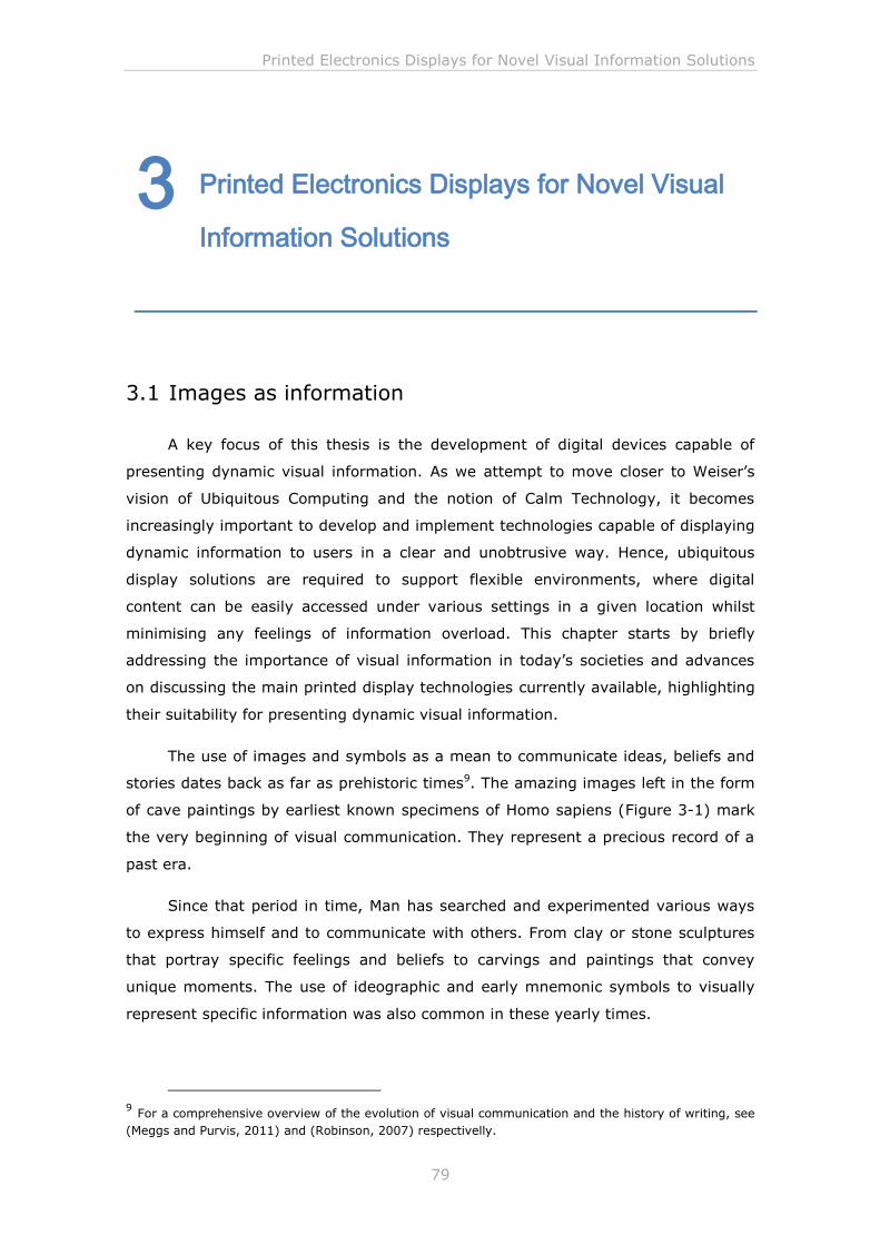
Printed Electronics Displays for Novel Visual Information Solutions
79
3 Printed Electronics Displays for Novel Visual
Information Solutions
3.1 Images as information
A key focus of this thesis is the development of digital devices capable of
presenting dynamic visual information. As we attempt to move closer to Weiser’s
vision of Ubiquitous Computing and the notion of Calm Technology, it becomes
increasingly important to develop and implement technologies capable of displaying
dynamic information to users in a clear and unobtrusive way. Hence, ubiquitous
display solutions are required to support flexible environments, where digital
content can be easily accessed under various settings in a given location whilst
minimising any feelings of information overload. This chapter starts by briefly
addressing the importance of visual information in today’s societies and advances
on discussing the main printed display technologies currently available, highlighting
their suitability for presenting dynamic visual information.
The use of images and symbols as a mean to communicate ideas, beliefs and
stories dates back as far as prehistoric times9. The amazing images left in the form
of cave paintings by earliest known specimens of Homo sapiens (Figure 3-1) mark
the very beginning of visual communication. They represent a precious record of a
past era.
Since that period in time, Man has searched and experimented various ways
to express himself and to communicate with others. From clay or stone sculptures
that portray specific feelings and beliefs to carvings and paintings that convey
unique moments. The use of ideographic and early mnemonic symbols to visually
represent specific information was also common in these yearly times.
9 For a comprehensive overview of the evolution of visual communication and the history of writing, see
(Meggs and Purvis, 2011) and (Robinson, 2007) respectivelly.
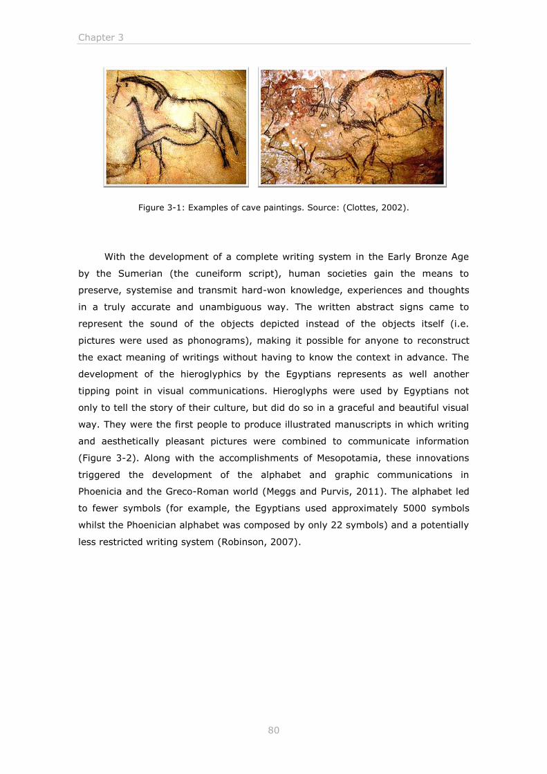
Chapter 3
80
Figure 3-1: Examples of cave paintings. Source: (Clottes, 2002).
With the development of a complete writing system in the Early Bronze Age
by the Sumerian (the cuneiform script), human societies gain the means to
preserve, systemise and transmit hard-won knowledge, experiences and thoughts
in a truly accurate and unambiguous way. The written abstract signs came to
represent the sound of the objects depicted instead of the objects itself (i.e.
pictures were used as phonograms), making it possible for anyone to reconstruct
the exact meaning of writings without having to know the context in advance. The
development of the hieroglyphics by the Egyptians represents as well another
tipping point in visual communications. Hieroglyphs were used by Egyptians not
only to tell the story of their culture, but did do so in a graceful and beautiful visual
way. They were the first people to produce illustrated manuscripts in which writing
and aesthetically pleasant pictures were combined to communicate information
(Figure 3-2). Along with the accomplishments of Mesopotamia, these innovations
triggered the development of the alphabet and graphic communications in
Phoenicia and the Greco-Roman world (Meggs and Purvis, 2011). The alphabet led
to fewer symbols (for example, the Egyptians used approximately 5000 symbols
whilst the Phoenician alphabet was composed by only 22 symbols) and a potentially
less restricted writing system (Robinson, 2007).
Printed Electronics Displays for Novel Visual Information Solutions
81
Figure 3-2: Example of an Egyptian illustrated manuscript (Papyrus of Hunefer). Source:
(Meggs and Purvis, 2011).
Throughout the centuries, the use of visual elements to communicate
information continued to evolve, accommodating new technologies (for example,
the printing press) and forms of communication and expression. In the late 1800s,
with the improvements made in the motion picture camera, the idea of creating
continuous live action became attainable. By making sequential drawings of a
continuing action and projecting them onto a screen at a constant rate, it became
possible not only to re-create the movements and actions of any living being but as
well as to give life to animated objects. Moreover, it was possible to show feelings
and emotions in a figure with which the audience actually could become
compassionate about (Thomas and Johnston, 1997). Animated graphic soon
became an effective method of entertainment as well as of presenting information.
The advent of computers and the internet further pushed the limits of visual
communication into new creative directions. It not only enabled new forms of
communication and entertainment but also it made available means and tools that
increasingly impacted the traditional design and animation practices, facilitating and
speeding the production process (Furniss, 2008). Changes of layout, typography or
any other graphic element can now be instantly seen without the need of printing,
and endless versions of the same work can be easily made. New procedures related
to image manipulation and 3D image creation also became available at processing
times that could not be done before. The internet on the other hand, provided an
easily accessible and affordable medium for exhibition and dissemination of
contents with today’s websites often integrating multiple disciplines of information
systems, information technology and communication design.
Chapter 3
82
The clarity and power that visual elements can offer makes today visual
communication a method of choice for conveying information. For example, signs,
signage systems, posters and maps are widely used in public spaces such as in
airports, train stations, hospitals, museums, schools, or libraries to provide visual
directions and instructions. Or, icons and symbols are implemented in vehicles,
household appliances, and computers to offer visual clues about specific operating
functions.
3.2 Electronic “paper” displays
The compelling need to present information as text and images has led to the
development of many different electronic display technologies. The range of options
is already high, with each having their own advantages and disadvantages. If we
consider the currently available electronic display technologies, it is possible to
divide them, according to their lighting source, into two distinct classes: emissive
and non-emissive electronic displays (see for instance, (Kahn and Zervos, 2008;
Lee et al., 2008)).
In emissive displays, each picture element has the capability to emit its own
light. They convert electrical energy into light that serves to illuminate the display
screen and form the image. This type of displays perform very well in environments
where the luminosity can be controlled or under dark conditions, but tend to lose its
viewability, either partially or totally in very bright conditions such as under direct
sunlight, where the reflection of ambient light matches or exceeds the light
emission from the display (Amundson, 2005; Lee et al., 2008). Examples of
emissive devices and technologies include the cathode ray tube displays, field
emission displays, plasma displays, electroluminescent displays, and organic light
emitting diode displays.
In contrast, non-emissive displays do not emit light and, instead, use optical
effects to convert sunlight or light from some external source into graphic patterns.
Each picture element operates as an independent light switch, modulating incident
light. If the light source is behind the display panel (i.e. a backlight unit is used),
the display operates in transmissive mode. Alternatively, ambient light can be used
as the light source, and the display is said to operate in reflective mode. Since no
backlight is needed in reflective displays, the power consumption of these displays
is relatively low (Lee et al., 2008). In addition, novel non-emissive reflective
displays are bistable, i.e. their images remain in a non-power-consuming state
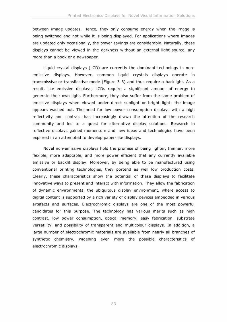
Printed Electronics Displays for Novel Visual Information Solutions
83
between image updates. Hence, they only consume energy when the image is
being switched and not while it is being displayed. For applications where images
are updated only occasionally, the power savings are considerable. Naturally, these
displays cannot be viewed in the darkness without an external light source, any
more than a book or a newspaper.
Liquid crystal displays (LCD) are currently the dominant technology in non-
emissive displays. However, common liquid crystals displays operate in
transmissive or transflective mode (Figure 3-3) and thus require a backlight. As a
result, like emissive displays, LCDs require a significant amount of energy to
generate their own light. Furthermore, they also suffer from the same problem of
emissive displays when viewed under direct sunlight or bright light: the image
appears washed out. The need for low power consumption displays with a high
reflectivity and contrast has increasingly drawn the attention of the research
community and led to a quest for alternative display solutions. Research in
reflective displays gained momentum and new ideas and technologies have been
explored in an attempted to develop paper-like displays.
Novel non-emissive displays hold the promise of being lighter, thinner, more
flexible, more adaptable, and more power efficient that any currently available
emissive or backlit display. Moreover, by being able to be manufactured using
conventional printing technologies, they portend as well low production costs.
Clearly, these characteristics show the potential of these displays to facilitate
innovative ways to present and interact with information. They allow the fabrication
of dynamic environments, the ubiquitous display environment, where access to
digital content is supported by a rich variety of display devices embedded in various
artefacts and surfaces. Electrochromic displays are one of the most powerful
candidates for this purpose. The technology has various merits such as high
contrast, low power consumption, optical memory, easy fabrication, substrate
versatility, and possibility of transparent and multicolour displays. In addition, a
large number of electrochromic materials are available from nearly all branches of
synthetic chemistry, widening even more the possible characteristics of
electrochromic displays.
Chapter 3
84
Figure 3-3: Non-emissive displays operation modes: a) transmissive, b) reflective, and c)
transflective.
Examples of non-emissive reflective displays include, but are not limited to,
electrophoretic displays, electrochromic displays, thermochromic displays,
electrowetting displays and photonic crystals displays. In the following subsections
it is presented a review of these emergent non-emissive display technologies,
describing their functioning, main advantages, challenges, and current (or possible)
applications, with a special focus on electrochromic devices. All the technologies
reviewed aspire to a certain extend reproduce the visual experience of conventional
printed media as seen in books and newspapers. A comparison between the various
technologies is provided in section 3.3.
3.2.1 Electrochromic displays
A material is considered to be electrochromic when it exhibits a perceptible
colour change in the visible region of the electromagnetic spectrum as a result of an
electrical stimulus10. This functions by a reversible electrochemical redox reaction
10
Although this is the typical working definition of electrochromism, and the one adopted for the
purpose of this thesis, research in electrochromic devices for multispectral energy modulation has
extended it to include also modulation of radiation in the infrared (see for instance, (Franke et al., 2000;
Topart and Hourquebie, 1999)) and microwave (see (Rose et al., 1997)) regions. Hence, under this new
definition, “colour” can mean a response of detectors to these electromagnetic regions, and not just by
the human eye (Rowley and Mortimer, 2002).
a) b)
c)
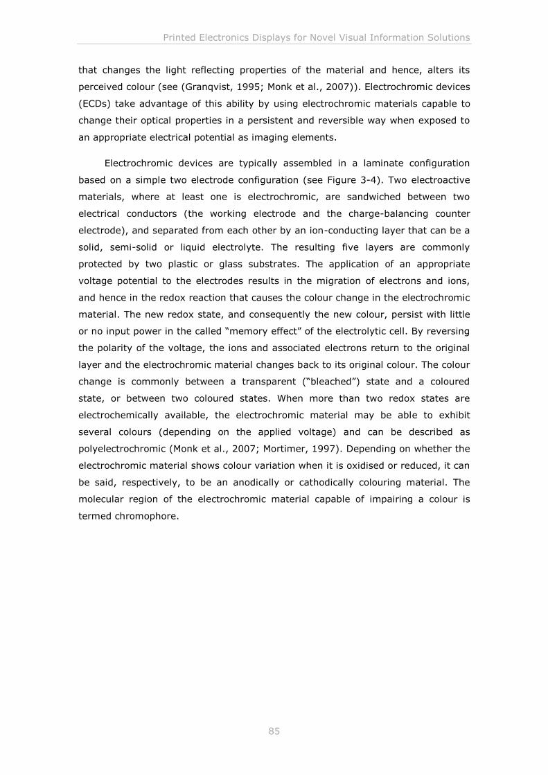
Printed Electronics Displays for Novel Visual Information Solutions
85
that changes the light reflecting properties of the material and hence, alters its
perceived colour (see (Granqvist, 1995; Monk et al., 2007)). Electrochromic devices
(ECDs) take advantage of this ability by using electrochromic materials capable to
change their optical properties in a persistent and reversible way when exposed to
an appropriate electrical potential as imaging elements.
Electrochromic devices are typically assembled in a laminate configuration
based on a simple two electrode configuration (see Figure 3-4). Two electroactive
materials, where at least one is electrochromic, are sandwiched between two
electrical conductors (the working electrode and the charge-balancing counter
electrode), and separated from each other by an ion-conducting layer that can be a
solid, semi-solid or liquid electrolyte. The resulting five layers are commonly
protected by two plastic or glass substrates. The application of an appropriate
voltage potential to the electrodes results in the migration of electrons and ions,
and hence in the redox reaction that causes the colour change in the electrochromic
material. The new redox state, and consequently the new colour, persist with little
or no input power in the called “memory effect” of the electrolytic cell. By reversing
the polarity of the voltage, the ions and associated electrons return to the original
layer and the electrochromic material changes back to its original colour. The colour
change is commonly between a transparent (“bleached”) state and a coloured
state, or between two coloured states. When more than two redox states are
electrochemically available, the electrochromic material may be able to exhibit
several colours (depending on the applied voltage) and can be described as
polyelectrochromic (Monk et al., 2007; Mortimer, 1997). Depending on whether the
electrochromic material shows colour variation when it is oxidised or reduced, it can
be said, respectively, to be an anodically or cathodically colouring material. The
molecular region of the electrochromic material capable of impairing a colour is
termed chromophore.
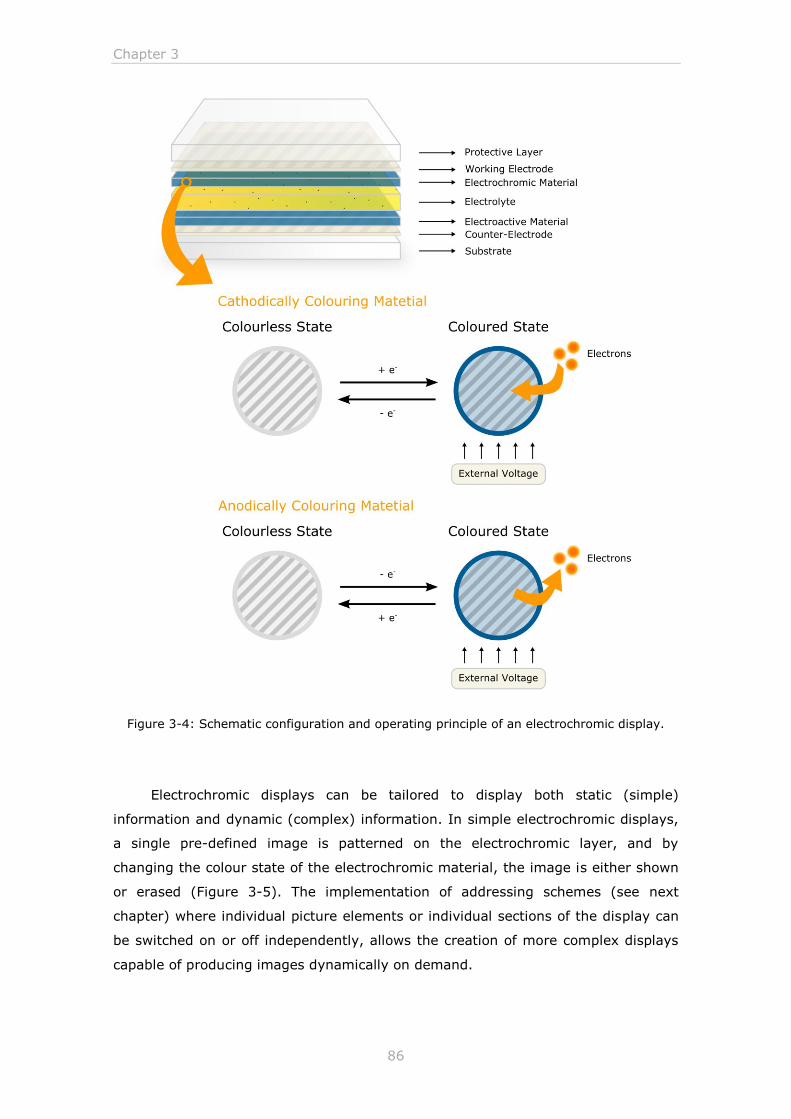
Chapter 3
86
Figure 3-4: Schematic configuration and operating principle of an electrochromic display.
Electrochromic displays can be tailored to display both static (simple)
information and dynamic (complex) information. In simple electrochromic displays,
a single pre-defined image is patterned on the electrochromic layer, and by
changing the colour state of the electrochromic material, the image is either shown
or erased (Figure 3-5). The implementation of addressing schemes (see next
chapter) where individual picture elements or individual sections of the display can
be switched on or off independently, allows the creation of more complex displays
capable of producing images dynamically on demand.
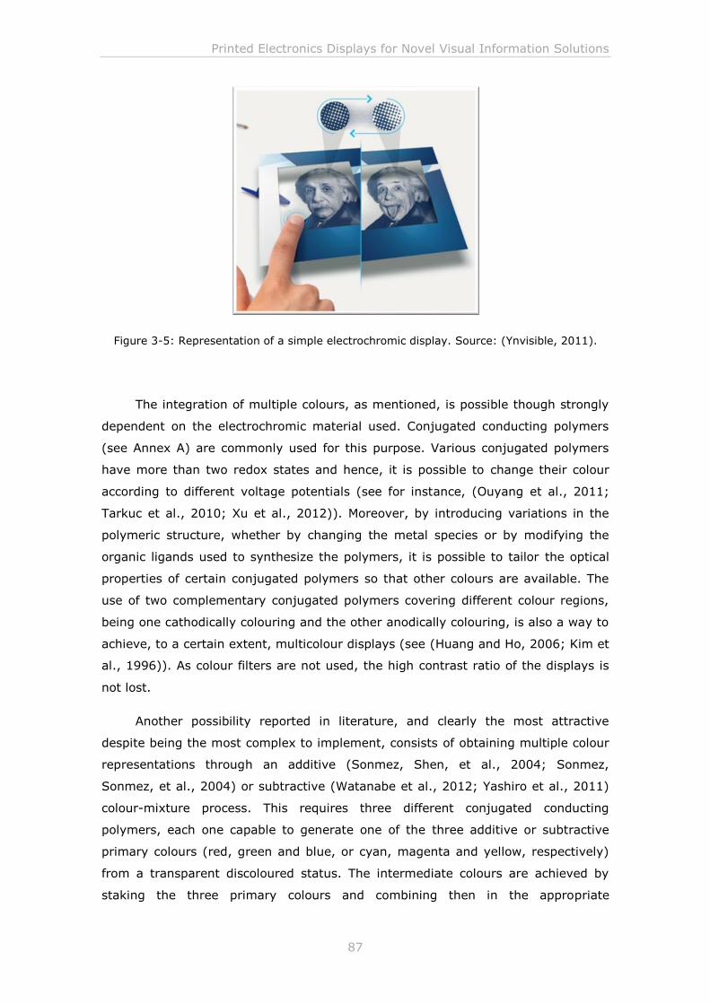
Printed Electronics Displays for Novel Visual Information Solutions
87
Figure 3-5: Representation of a simple electrochromic display. Source: (Ynvisible, 2011).
The integration of multiple colours, as mentioned, is possible though strongly
dependent on the electrochromic material used. Conjugated conducting polymers
(see Annex A) are commonly used for this purpose. Various conjugated polymers
have more than two redox states and hence, it is possible to change their colour
according to different voltage potentials (see for instance, (Ouyang et al., 2011;
Tarkuc et al., 2010; Xu et al., 2012)). Moreover, by introducing variations in the
polymeric structure, whether by changing the metal species or by modifying the
organic ligands used to synthesize the polymers, it is possible to tailor the optical
properties of certain conjugated polymers so that other colours are available. The
use of two complementary conjugated polymers covering different colour regions,
being one cathodically colouring and the other anodically colouring, is also a way to
achieve, to a certain extent, multicolour displays (see (Huang and Ho, 2006; Kim et
al., 1996)). As colour filters are not used, the high contrast ratio of the displays is
not lost.
Another possibility reported in literature, and clearly the most attractive
despite being the most complex to implement, consists of obtaining multiple colour
representations through an additive (Sonmez, Shen, et al., 2004; Sonmez,
Sonmez, et al., 2004) or subtractive (Watanabe et al., 2012; Yashiro et al., 2011)
colour-mixture process. This requires three different conjugated conducting
polymers, each one capable to generate one of the three additive or subtractive
primary colours (red, green and blue, or cyan, magenta and yellow, respectively)
from a transparent discoloured status. The intermediate colours are achieved by
staking the three primary colours and combining then in the appropriate
Chapter 3
88
proportions. The display is assembled in a multi-layered structure divided into a
frontplane and backplane (see, (Yashiro et al., 2011)). The frontplane is formed by
three superimposed transparent electrodes, each having an electrochromic layer
associated to, and separated by insulating layers; and one white reflecting layer.
Each electrochromic layer is based on three kinds of organic electrochromic
compounds capable to generate one of the three primary colours. The backplane
consist of the counter-electrode and is linked to the frontplane through the
electrolyte. The structure reduces the light loss to reproduce colour by
superimposing the three primary colours, likewise it is done with printing colour on
paper.
The main advantages of electrochromic displays are their low power
consumption and low manufacture cost. The memory effect of the electrolytic cell
ensures that electrochromic displays only require energy when switching between
images (i.e. they are bistable). The nature and availability of the raw materials
used to produce this type of displays, along with the simplicity of the manufacture
process, ensure the low production cost. In addition, electrochromic displays are
characterised for having a high reflectivity and a high contrast, presenting the same
agreeable readability as printed paper, whether in direct sunlight or in dimmed
light.
The main disadvantages of this technology are the lack of resolution of other
commercially available display technologies, the limited variety of available colours
in large scale production, and the slow response times. As a consequence,
electrochromic displays are more suitable for applications requiring simple displays
that involve long-term display of information, such as re-usable price labels,
advertising billboards and digital signage; or for being incorporated in disposable
devices such as smart cards, greeting cards or product packages. Whilst there are
many proposed applications for electrochromic devices (see for instance, (Bamfield
and Hutchings, 2010; Monk et al., 2007)), until now the most successful
commercial applications have been limited to automatically dimming, anti-glare
automobile rear-view mirrors (see for instance, (Baucke, 1987; Liu and Richardson,
2005; Lynam, 1987)) and electrically shaded smart-windows (see (Baetens et al.,
2010; Cinnsealach et al., 1998; Granqvist et al., 1997; Heuer et al., 2002;
Niklasson and Granqvist, 2007; Rauh, 1999)). Both applications are reported in a
great number of patents.
Printed Electronics Displays for Novel Visual Information Solutions
89
3.2.2 Electrophoretic displays
An electrophoretic display is a reflective display that functions based on the
electro-static rearrangement of charged, light-scattering, pigment particles
suspended in a dielectric fluid, in response to an externally applied electric field.
This suspension, commonly called “electronic ink” or “electrophoretic ink”, is the
key component of electrophoretic displays.
The first electrophoretic display was reported in 1973, by Ota et al. (1973),
however, it was only in the late nineties that research in electrophoretic displays
boomed. Comiskey et al. (1998) demonstrated the first example of a
microencapsulated electrophoretic displays, and subsequent work developed by
E Ink Corporation11 led to dramatic improvements in the technology (see for
instance, (Albert et al., 2000, 2001; Jacobson et al., 2001; Loxley and Comiskey,
2001)), and to the first products being commercialised (E Ink, 2004). Nowadays, E
Ink Corporation continues to be the reference producer of electrophoretic displays.
In E Ink’s electronic ink (Chen et al., 2003; E Ink, 2012g), millions of
microcapsules, each about a micrometer in diameter, are suspended in a carrier
solution of hydrocarbons and black dye. Each microcapsule contains positively
charged white particles (usually titanium dioxide particles) and negatively charged
black particles (usually carbon black) in a clear fluid. The basic operating principle
of this two-particle microencapsulated system is illustrated in Figure 3-6. When a
positive electric field is applied to the bottom surface of a microcapsule, the
positively charged white particles are driven to the top of the microcapsule, where
they become visible to the user. At the same time, an opposite electric field pulls
down the negatively charged black particles. As the particles tend to form a solid
layer across the face of the microcapsule, the particles at the top hide the particles
at the bottom. Hence, the black particles become concealed to the user. At the top,
the titanium dioxide particles reflect the incident light in all directions, and the
surface of the display appears white at that point. By reversing the voltage, the
black particles migrate to the top of the microcapsule and the white to the bottom.
As a result, the surface of the display at that point appears now dark, since the
incident light is absorbed by the black dye. By dividing the display into a number of
small picture elements, i.e. into pixels, different precise points of its surface can be
addressed and manipulated independently. Images can them be easily formed by
applying the appropriate electrical charge to each pixel and thus create a pattern of
reflecting and absorbing regions.
11
http://www.eink.com/
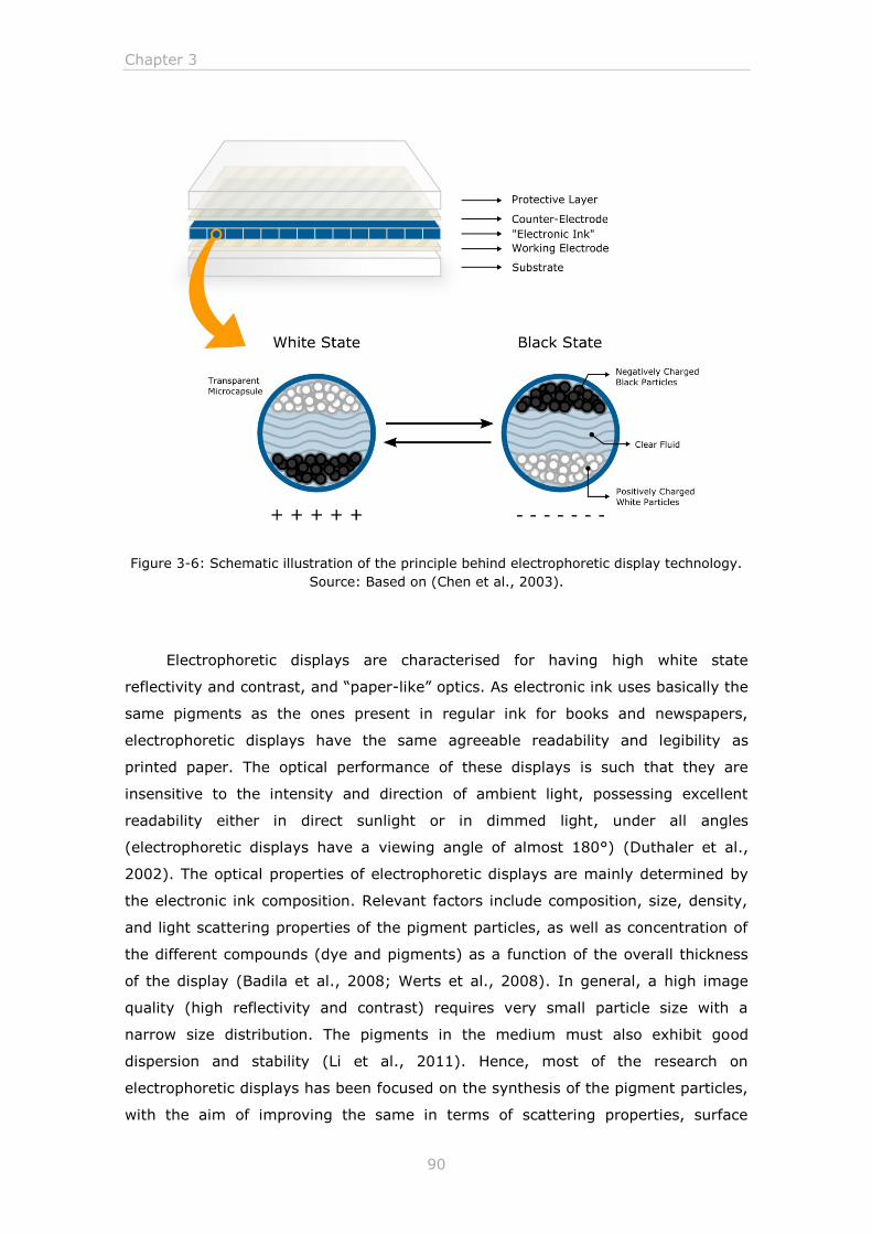
Chapter 3
90
Figure 3-6: Schematic illustration of the principle behind electrophoretic display technology.
Source: Based on (Chen et al., 2003).
Electrophoretic displays are characterised for having high white state
reflectivity and contrast, and “paper-like” optics. As electronic ink uses basically the
same pigments as the ones present in regular ink for books and newspapers,
electrophoretic displays have the same agreeable readability and legibility as
printed paper. The optical performance of these displays is such that they are
insensitive to the intensity and direction of ambient light, possessing excellent
readability either in direct sunlight or in dimmed light, under all angles
(electrophoretic displays have a viewing angle of almost 180°) (Duthaler et al.,
2002). The optical properties of electrophoretic displays are mainly determined by
the electronic ink composition. Relevant factors include composition, size, density,
and light scattering properties of the pigment particles, as well as concentration of
the different compounds (dye and pigments) as a function of the overall thickness
of the display (Badila et al., 2008; Werts et al., 2008). In general, a high image
quality (high reflectivity and contrast) requires very small particle size with a
narrow size distribution. The pigments in the medium must also exhibit good
dispersion and stability (Li et al., 2011). Hence, most of the research on
electrophoretic displays has been focused on the synthesis of the pigment particles,
with the aim of improving the same in terms of scattering properties, surface
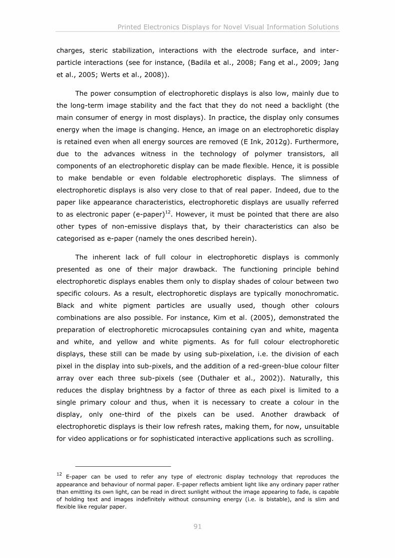
Printed Electronics Displays for Novel Visual Information Solutions
91
charges, steric stabilization, interactions with the electrode surface, and inter-
particle interactions (see for instance, (Badila et al., 2008; Fang et al., 2009; Jang
et al., 2005; Werts et al., 2008)).
The power consumption of electrophoretic displays is also low, mainly due to
the long-term image stability and the fact that they do not need a backlight (the
main consumer of energy in most displays). In practice, the display only consumes
energy when the image is changing. Hence, an image on an electrophoretic display
is retained even when all energy sources are removed (E Ink, 2012g). Furthermore,
due to the advances witness in the technology of polymer transistors, all
components of an electrophoretic display can be made flexible. Hence, it is possible
to make bendable or even foldable electrophoretic displays. The slimness of
electrophoretic displays is also very close to that of real paper. Indeed, due to the
paper like appearance characteristics, electrophoretic displays are usually referred
to as electronic paper (e-paper)12. However, it must be pointed that there are also
other types of non-emissive displays that, by their characteristics can also be
categorised as e-paper (namely the ones described herein).
The inherent lack of full colour in electrophoretic displays is commonly
presented as one of their major drawback. The functioning principle behind
electrophoretic displays enables them only to display shades of colour between two
specific colours. As a result, electrophoretic displays are typically monochromatic.
Black and white pigment particles are usually used, though other colours
combinations are also possible. For instance, Kim et al. (2005), demonstrated the
preparation of electrophoretic microcapsules containing cyan and white, magenta
and white, and yellow and white pigments. As for full colour electrophoretic
displays, these still can be made by using sub-pixelation, i.e. the division of each
pixel in the display into sub-pixels, and the addition of a red-green-blue colour filter
array over each three sub-pixels (see (Duthaler et al., 2002)). Naturally, this
reduces the display brightness by a factor of three as each pixel is limited to a
single primary colour and thus, when it is necessary to create a colour in the
display, only one-third of the pixels can be used. Another drawback of
electrophoretic displays is their low refresh rates, making them, for now, unsuitable
for video applications or for sophisticated interactive applications such as scrolling.
12
E-paper can be used to refer any type of electronic display technology that reproduces the
appearance and behaviour of normal paper. E-paper reflects ambient light like any ordinary paper rather
than emitting its own light, can be read in direct sunlight without the image appearing to fade, is capable
of holding text and images indefinitely without consuming energy (i.e. is bistable), and is slim and
flexible like regular paper.
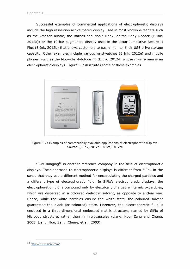
Chapter 3
92
Successful examples of commercial applications of electrophoretic displays
include the high resolution active matrix display used in most known e-readers such
as the Amazon Kindle, the Barnes and Noble Nook, or the Sony Reader (E Ink,
2012a); or the 10-bar segmented display used in the Lexar JumpDrive Secure II
Plus (E Ink, 2012b) that allows customers to easily monitor their USB drive storage
capacity. Other examples include various wristwatches (E Ink, 2012e) and mobile
phones, such as the Motorola Motofone F3 (E Ink, 2012d) whose main screen is an
electrophoretic displays. Figure 3-7 illustrates some of these examples.
Figure 3-7: Examples of commercially available applications of electrophoretic displays.
Source: (E Ink, 2012b, 2012c, 2012f).
SiPix Imaging13 is another reference company in the field of electrophoretic
displays. Their approach to electrophoretic displays is different from E Ink in the
sense that they use a different method for encapsulating the charged particles and
a different type of electrophoretic fluid. In SiPix’s electrophoretic displays, the
electrophoretic fluid is composed only by electrically charged white micro-particles,
which are dispersed in a coloured dielectric solvent, as opposite to a clear one.
Hence, while the white particles ensure the white state, the coloured solvent
guarantees the black (or coloured) state. Moreover, the electrophoretic fluid is
enclosed in a three-dimensional embossed matrix structure, named by SiPix of
Microcup structure, rather than in microcapsules (Liang, Hou, Zang and Chung,
2003; Liang, Hou, Zang, Chung, et al., 2003).
13
http://www.sipix.com/
Printed Electronics Displays for Novel Visual Information Solutions
93
3.2.3 Quick-response liquid powder displays
Quick-response liquid powder displays (QR-LPD) operate in a very similar way
to electrophoretic displays. The displays are composed by two types of powder, one
with white colour and negative charge, and the other with black colour and positive
charge (see, (Hattori et al., 2003, 2004, 2010)). Both types of powder are placed
together into an area between two patterned substrates. Separators are used to
form cells gaps and prevent the mixing up of powders between adjacent pixels and
ensure the uniform distribution of the powders within each pixel. The rest of the
space in the cell is filled with air. The powders are attracted to each other and make
a mass with grey colour, yet each powder behaves just like a liquid by itself. It is
the extremely high liquidity of the powders that allows the use of the term “Liquid
Powder” for this material (i.e. the materials have a powder form but show a liquid
behaviour). When a negative voltage is applied to the upper transparent electrode,
the positively charged black powder moves to the upper electrode exhibiting a black
appearance and, in the opposite bias case, the negatively charged white powder is
attracted to the upper electrode exhibiting a white appearance. Due to attraction
forces (electrical and non-electrical) between the electrodes and the liquid powder,
images can be maintained without electric power (Hattori et al., 2003, 2004, 2010).
However, separating the charged powder pigments from each other and from the
electrodes requires significant force (unlike in liquid dispersed pigments in
electrophoretic displays). As a result, operating voltages are high (around 40V to
70V) (Hattori et al., 2004, 2005; Heikenfeld et al., 2011; Sakurai et al., 2007).
QR-LPD present response times of less than 0.2 msec, bright images with a
paper-white appearance with more than 40% in reflectivity, bi-stability, wide
viewing angle with nearly ideal diffuse reflectance, large matrix-addressing
capability by passive-matrix driving, and halftone images with more than four gray
levels (Hattori et al., 2004). Colour displays were also demonstrated using two
different methods (Sakurai et al., 2006). The first method consisted of using colour
liquid powder to produce coloured monochromatic displays, while the second
method consisted of applying colour filter technology (RGB colour filter) with black
and white liquid powder to produce a full colour displays (Figure 3-8).
Chapter 3
94
Figure 3-8: Picture of a full-colour quick-response liquid powder display. Source: (Hattori et
al., 2010).
QR-LPD technology was first demonstrated in 2003 (Hattori et al., 2003), by
Bridgestone Corporation14. In 2012, however, Bridgestone announced its plans to
withdraw from the electronic paper business and abandon the research on quick-
response liquid powder displays (Bridgestone, 2012).
3.2.4 Electrowetting displays
Electrowetting displays employ principles of microfluidic to manipulate the
shape of a confined water-oil interface through an applied voltage (see (Hayes and
Feenstra, 2003; Pollack et al., 2000)). Each pixel of the display is formed by an
optical stack comprising of a white (reflecting) substrate, a hydrophobic insulator, a
droplet of coloured oil and water (see Figure 3-9).
In equilibrium, the droplet of coloured oil forms a continuous film between the
water and the hydrophobic insulator, resulting in a coloured pixel in the display.
However, when an electrical potential is applied across the hydrophobic insulator,
the interfacial tension between the water and the hydrophobic insulator changes,
and the initial stacked state is no longer energetically favourable. As a result, the
system proceeds to lower its energy by moving the water into contact with the
insulator, and thus displacing the oil. The underlying subtract becomes visible, and
the optical properties of the stack are changed from a coloured off-state (due to the
colour of the oil) to a white reflective on-state (due to the colour of the subtract
where the droplet of oil is placed). Still, the size of the pixel must be sufficiently
14 http://www.bridgestone.com/
Printed Electronics Displays for Novel Visual Information Solutions
95
small so that the viewer does not see the droplet of oil contracted, and instead
experiences the average optical response (Feenstra et al., 2004; Hayes and
Feenstra, 2003). When the voltage is removed, the oil droplet returns to is initial
state.
Figure 3-9: Schematic illustration of the principle behind electrowetting display technology.
Source: Based on (Feenstra et al., 2004).
Electrowetting technology can be used to produce simple black and white
displays, or to produce a wide range of displays with different colours, simply by
applying different dyes with different colours (Figure 3-10). Multiple colours
displays can be achieved either by using the single layer architecture described
above with a black coloured dye and a multiple colour filter (i.e. employing sub-
pixelation), or by implementing a three layer architecture, where each layer
correspond to a different monochromic colour. In this type of setting, the layers
function independently of each other, and are activated by the same oil dosing
process that is performed on single layers. Since any colour can be generated
anywhere in the display surface, the optical performance increases with a factor of
three with respect to the single layer structure.
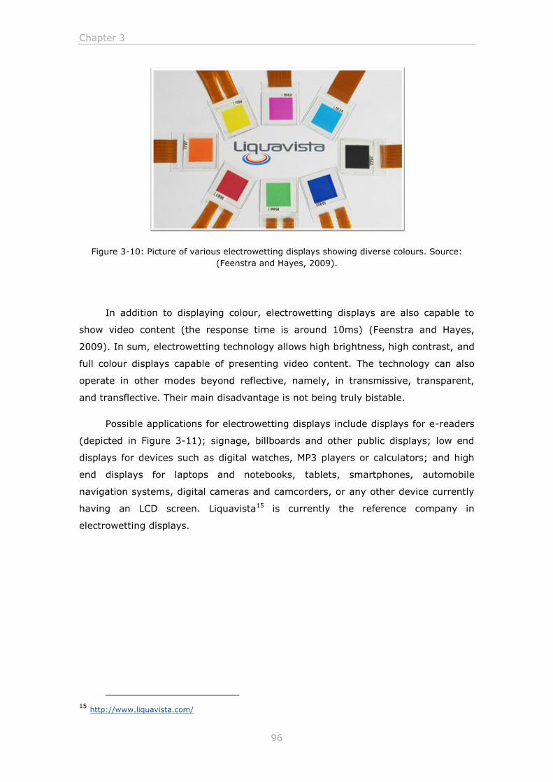
Chapter 3
96
Figure 3-10: Picture of various electrowetting displays showing diverse colours. Source:
(Feenstra and Hayes, 2009).
In addition to displaying colour, electrowetting displays are also capable to
show video content (the response time is around 10ms) (Feenstra and Hayes,
2009). In sum, electrowetting technology allows high brightness, high contrast, and
full colour displays capable of presenting video content. The technology can also
operate in other modes beyond reflective, namely, in transmissive, transparent,
and transflective. Their main disadvantage is not being truly bistable.
Possible applications for electrowetting displays include displays for e-readers
(depicted in Figure 3-11); signage, billboards and other public displays; low end
displays for devices such as digital watches, MP3 players or calculators; and high
end displays for laptops and notebooks, tablets, smartphones, automobile
navigation systems, digital cameras and camcorders, or any other device currently
having an LCD screen. Liquavista15 is currently the reference company in
electrowetting displays.
15 http://www.liquavista.com/
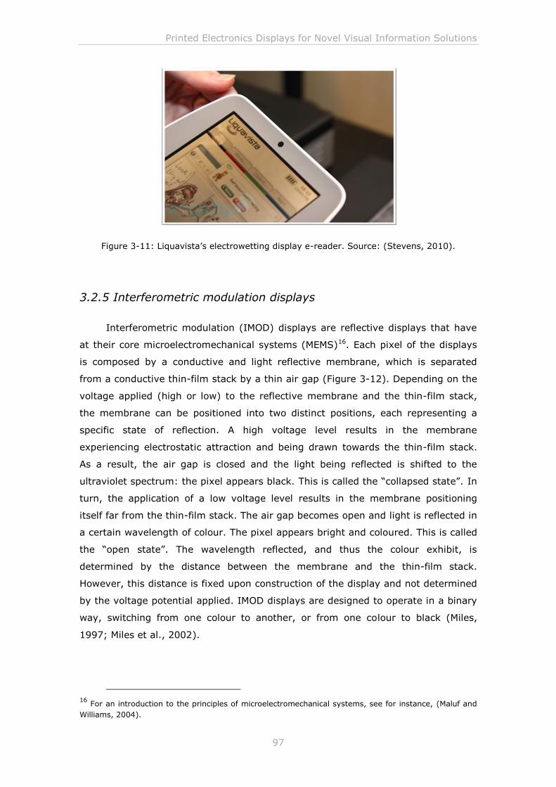
Printed Electronics Displays for Novel Visual Information Solutions
97
Figure 3-11: Liquavista’s electrowetting display e-reader. Source: (Stevens, 2010).
3.2.5 Interferometric modulation displays
Interferometric modulation (IMOD) displays are reflective displays that have
at their core microelectromechanical systems (MEMS)16. Each pixel of the displays
is composed by a conductive and light reflective membrane, which is separated
from a conductive thin-film stack by a thin air gap (Figure 3-12). Depending on the
voltage applied (high or low) to the reflective membrane and the thin-film stack,
the membrane can be positioned into two distinct positions, each representing a
specific state of reflection. A high voltage level results in the membrane
experiencing electrostatic attraction and being drawn towards the thin-film stack.
As a result, the air gap is closed and the light being reflected is shifted to the
ultraviolet spectrum: the pixel appears black. This is called the “collapsed state”. In
turn, the application of a low voltage level results in the membrane positioning
itself far from the thin-film stack. The air gap becomes open and light is reflected in
a certain wavelength of colour. The pixel appears bright and coloured. This is called
the “open state”. The wavelength reflected, and thus the colour exhibit, is
determined by the distance between the membrane and the thin-film stack.
However, this distance is fixed upon construction of the display and not determined
by the voltage potential applied. IMOD displays are designed to operate in a binary
way, switching from one colour to another, or from one colour to black (Miles,
1997; Miles et al., 2002).
16
For an introduction to the principles of microelectromechanical systems, see for instance, (Maluf and
Williams, 2004).
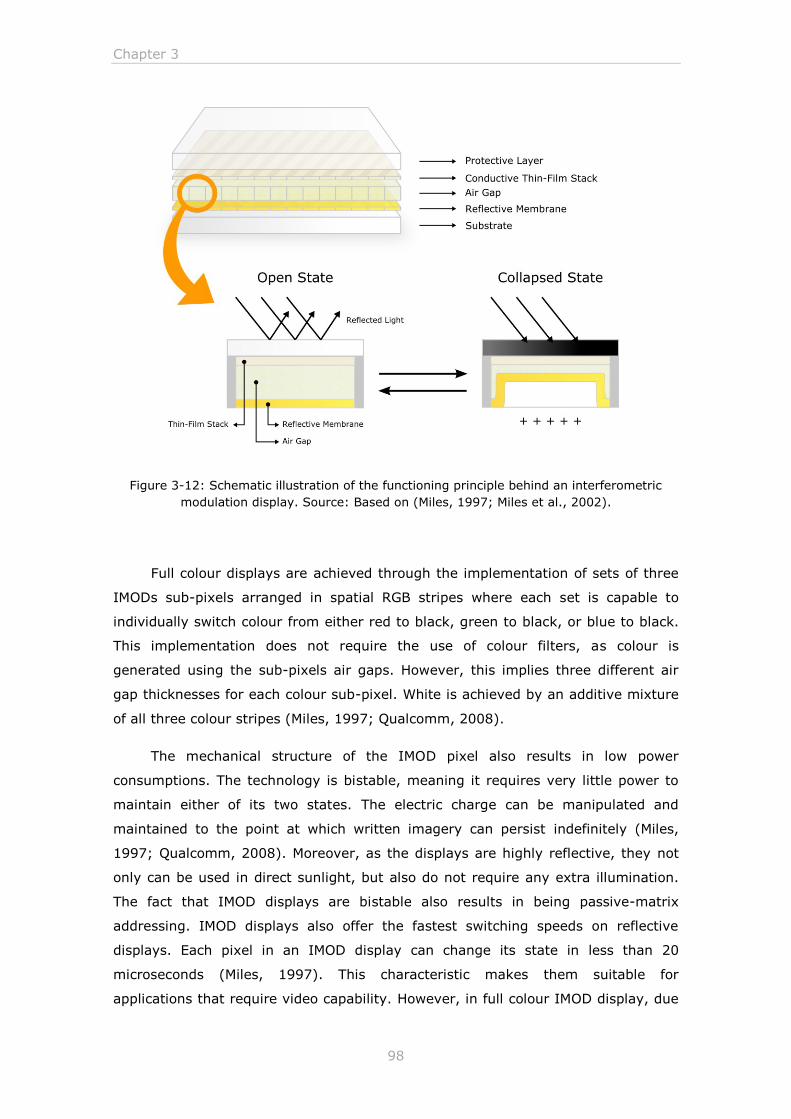
Chapter 3
98
Figure 3-12: Schematic illustration of the functioning principle behind an interferometric
modulation display. Source: Based on (Miles, 1997; Miles et al., 2002).
Full colour displays are achieved through the implementation of sets of three
IMODs sub-pixels arranged in spatial RGB stripes where each set is capable to
individually switch colour from either red to black, green to black, or blue to black.
This implementation does not require the use of colour filters, as colour is
generated using the sub-pixels air gaps. However, this implies three different air
gap thicknesses for each colour sub-pixel. White is achieved by an additive mixture
of all three colour stripes (Miles, 1997; Qualcomm, 2008).
The mechanical structure of the IMOD pixel also results in low power
consumptions. The technology is bistable, meaning it requires very little power to
maintain either of its two states. The electric charge can be manipulated and
maintained to the point at which written imagery can persist indefinitely (Miles,
1997; Qualcomm, 2008). Moreover, as the displays are highly reflective, they not
only can be used in direct sunlight, but also do not require any extra illumination.
The fact that IMOD displays are bistable also results in being passive-matrix
addressing. IMOD displays also offer the fastest switching speeds on reflective
displays. Each pixel in an IMOD display can change its state in less than 20
microseconds (Miles, 1997). This characteristic makes them suitable for
applications that require video capability. However, in full colour IMOD display, due
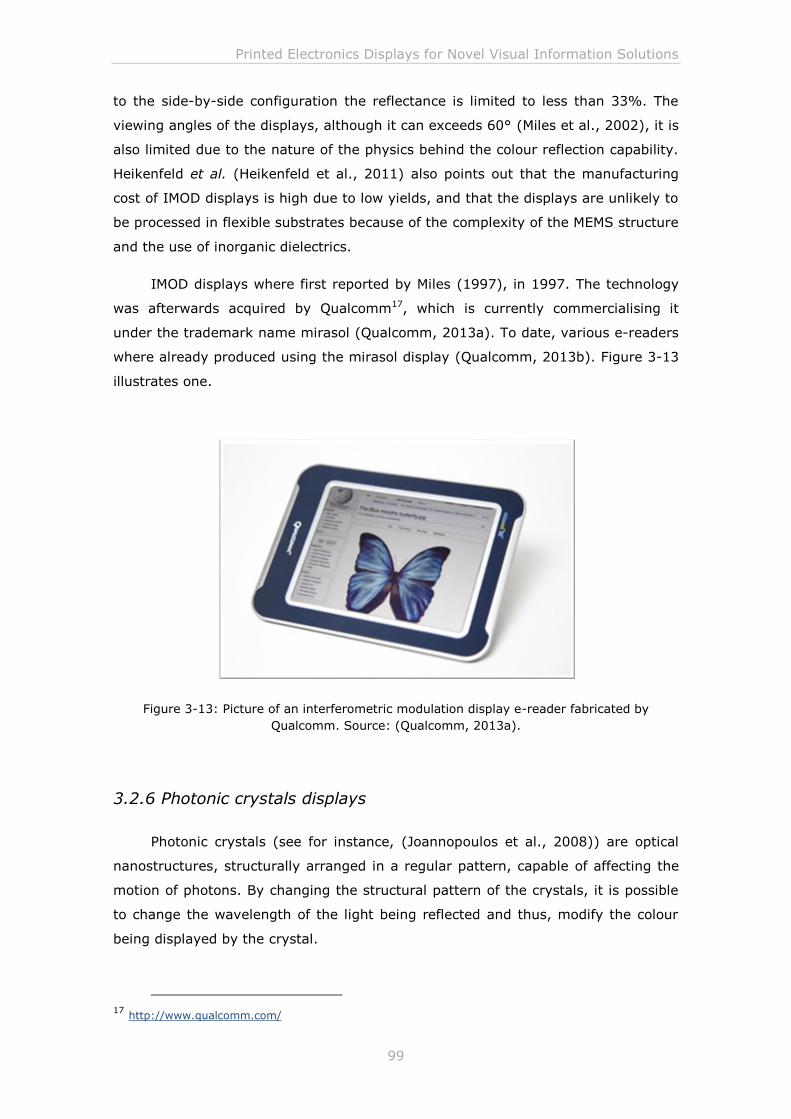
Printed Electronics Displays for Novel Visual Information Solutions
99
to the side-by-side configuration the reflectance is limited to less than 33%. The
viewing angles of the displays, although it can exceeds 60° (Miles et al., 2002), it is
also limited due to the nature of the physics behind the colour reflection capability.
Heikenfeld et al. (Heikenfeld et al., 2011) also points out that the manufacturing
cost of IMOD displays is high due to low yields, and that the displays are unlikely to
be processed in flexible substrates because of the complexity of the MEMS structure
and the use of inorganic dielectrics.
IMOD displays where first reported by Miles (1997), in 1997. The technology
was afterwards acquired by Qualcomm17, which is currently commercialising it
under the trademark name mirasol (Qualcomm, 2013a). To date, various e-readers
where already produced using the mirasol display (Qualcomm, 2013b). Figure 3-13
illustrates one.
Figure 3-13: Picture of an interferometric modulation display e-reader fabricated by
Qualcomm. Source: (Qualcomm, 2013a).
3.2.6 Photonic crystals displays
Photonic crystals (see for instance, (Joannopoulos et al., 2008)) are optical
nanostructures, structurally arranged in a regular pattern, capable of affecting the
motion of photons. By changing the structural pattern of the crystals, it is possible
to change the wavelength of the light being reflected and thus, modify the colour
being displayed by the crystal.
17 http://www.qualcomm.com/
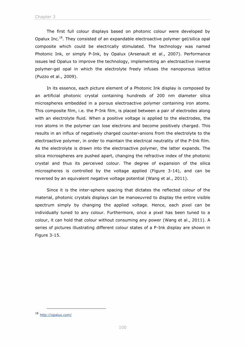
Chapter 3
100
The first full colour displays based on photonic colour were developed by
Opalux Inc.18. They consisted of an expandable electroactive polymer gel/silica opal
composite which could be electrically stimulated. The technology was named
Photonic Ink, or simply P-Ink, by Opalux (Arsenault et al., 2007). Performance
issues led Opalux to improve the technology, implementing an electroactive inverse
polymer-gel opal in which the electrolyte freely infuses the nanoporous lattice
(Puzzo et al., 2009).
In its essence, each picture element of a Photonic Ink display is composed by
an artificial photonic crystal containing hundreds of 200 nm diameter silica
microspheres embedded in a porous electroactive polymer containing iron atoms.
This composite film, i.e. the P-Ink film, is placed between a pair of electrodes along
with an electrolyte fluid. When a positive voltage is applied to the electrodes, the
iron atoms in the polymer can lose electrons and become positively charged. This
results in an influx of negatively charged counter-anions from the electrolyte to the
electroactive polymer, in order to maintain the electrical neutrality of the P-Ink film.
As the electrolyte is drawn into the electroactive polymer, the latter expands. The
silica microspheres are pushed apart, changing the refractive index of the photonic
crystal and thus its perceived colour. The degree of expansion of the silica
microspheres is controlled by the voltage applied (Figure 3-14), and can be
reversed by an equivalent negative voltage potential (Wang et al., 2011).
Since it is the inter-sphere spacing that dictates the reflected colour of the
material, photonic crystals displays can be manoeuvred to display the entire visible
spectrum simply by changing the applied voltage. Hence, each pixel can be
individually tuned to any colour. Furthermore, once a pixel has been tuned to a
colour, it can hold that colour without consuming any power (Wang et al., 2011). A
series of pictures illustrating different colour states of a P-Ink display are shown in
Figure 3-15.
18 http://opalux.com/
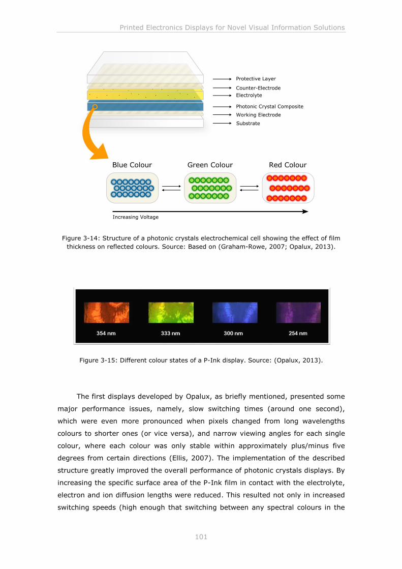
Printed Electronics Displays for Novel Visual Information Solutions
101
Figure 3-14: Structure of a photonic crystals electrochemical cell showing the effect of film
thickness on reflected colours. Source: Based on (Graham-Rowe, 2007; Opalux, 2013).
Figure 3-15: Different colour states of a P-Ink display. Source: (Opalux, 2013).
The first displays developed by Opalux, as briefly mentioned, presented some
major performance issues, namely, slow switching times (around one second),
which were even more pronounced when pixels changed from long wavelengths
colours to shorter ones (or vice versa), and narrow viewing angles for each single
colour, where each colour was only stable within approximately plus/minus five
degrees from certain directions (Ellis, 2007). The implementation of the described
structure greatly improved the overall performance of photonic crystals displays. By
increasing the specific surface area of the P-Ink film in contact with the electrolyte,
electron and ion diffusion lengths were reduced. This resulted not only in increased
switching speeds (high enough that switching between any spectral colours in the
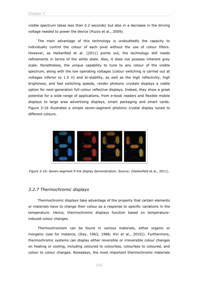
Chapter 3
102
visible spectrum takes less than 0.2 seconds) but also in a decrease in the driving
voltage needed to power the device (Puzzo et al., 2009).
The main advantage of this technology is undoubtedly the capacity to
individually control the colour of each pixel without the use of colour filters.
However, as Heikenfeld et al. (2011) points out, the technology still needs
refinements in terms of the white state. Also, it does not possess inherent grey
scale. Nonetheless, the unique capability to tune to any colour of the visible
spectrum, along with the low operating voltages (colour switching is carried out at
voltages inferior to 1.5 V) and bi-stability, as well as the high reflectivity, high
brightness, and fast switching speeds, render photonic crystals displays a viable
option for next-generation full-colour reflective displays. Indeed, they show a great
potential for a wide range of applications, from e-book readers and flexible mobile
displays to large area advertising displays, smart packaging and smart cards.
Figure 3-16 illustrates a simple seven-segment photonic crystal display tuned to
different colours.
Figure 3-16: Seven-segment P-Ink display demonstration. Source: (Heikenfeld et al., 2011).
3.2.7 Thermochromic displays
Thermochromic displays take advantage of the property that certain elements
or materials have to change their colour as a response to specific variations in the
temperature. Hence, thermochromic displays function based on temperature-
induced colour changes.
Thermochromism can be found in various materials, either organic or
inorganic (see for instance, (Day, 1963, 1968; Kiri et al., 2010)). Furthermore,
thermochromic systems can display either reversible or irreversible colour changes
on heating or cooling, including coloured to colourless, colourless to coloured, and
colour to colour changes. Nowadays, the most important thermochromic materials
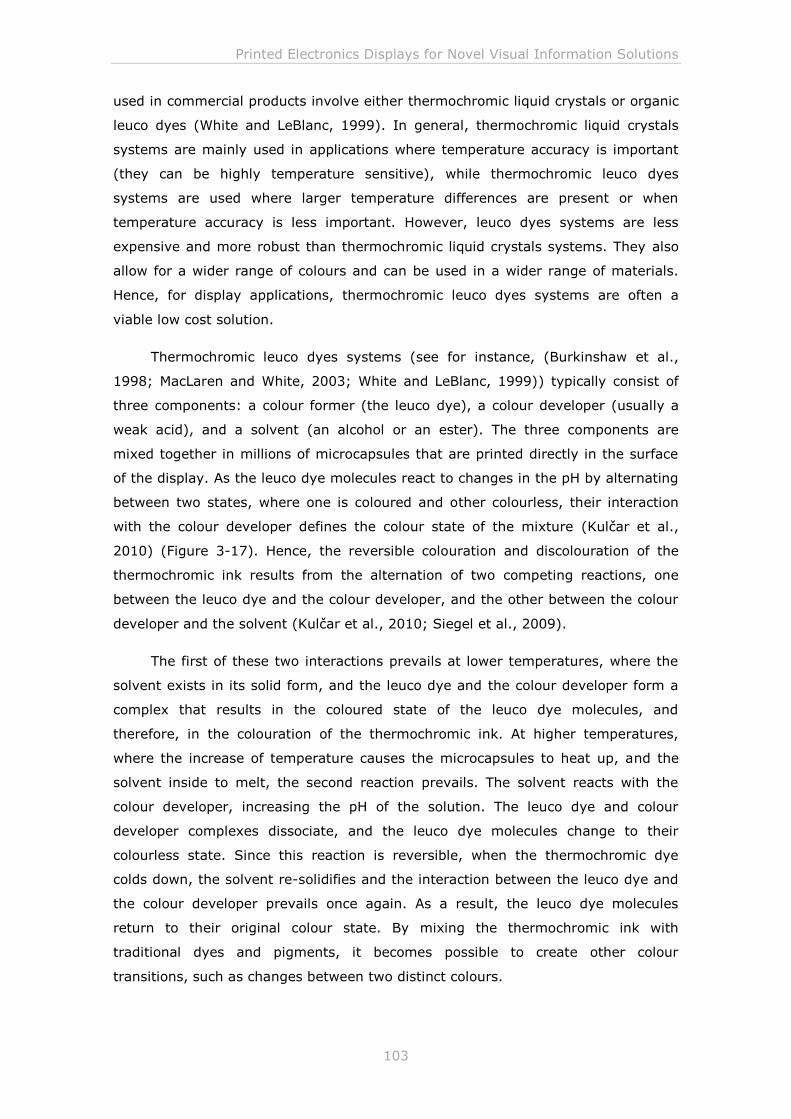
Printed Electronics Displays for Novel Visual Information Solutions
103
used in commercial products involve either thermochromic liquid crystals or organic
leuco dyes (White and LeBlanc, 1999). In general, thermochromic liquid crystals
systems are mainly used in applications where temperature accuracy is important
(they can be highly temperature sensitive), while thermochromic leuco dyes
systems are used where larger temperature differences are present or when
temperature accuracy is less important. However, leuco dyes systems are less
expensive and more robust than thermochromic liquid crystals systems. They also
allow for a wider range of colours and can be used in a wider range of materials.
Hence, for display applications, thermochromic leuco dyes systems are often a
viable low cost solution.
Thermochromic leuco dyes systems (see for instance, (Burkinshaw et al.,
1998; MacLaren and White, 2003; White and LeBlanc, 1999)) typically consist of
three components: a colour former (the leuco dye), a colour developer (usually a
weak acid), and a solvent (an alcohol or an ester). The three components are
mixed together in millions of microcapsules that are printed directly in the surface
of the display. As the leuco dye molecules react to changes in the pH by alternating
between two states, where one is coloured and other colourless, their interaction
with the colour developer defines the colour state of the mixture (Kulčar et al.,
2010) (Figure 3-17). Hence, the reversible colouration and discolouration of the
thermochromic ink results from the alternation of two competing reactions, one
between the leuco dye and the colour developer, and the other between the colour
developer and the solvent (Kulčar et al., 2010; Siegel et al., 2009).
The first of these two interactions prevails at lower temperatures, where the
solvent exists in its solid form, and the leuco dye and the colour developer form a
complex that results in the coloured state of the leuco dye molecules, and
therefore, in the colouration of the thermochromic ink. At higher temperatures,
where the increase of temperature causes the microcapsules to heat up, and the
solvent inside to melt, the second reaction prevails. The solvent reacts with the
colour developer, increasing the pH of the solution. The leuco dye and colour
developer complexes dissociate, and the leuco dye molecules change to their
colourless state. Since this reaction is reversible, when the thermochromic dye
colds down, the solvent re-solidifies and the interaction between the leuco dye and
the colour developer prevails once again. As a result, the leuco dye molecules
return to their original colour state. By mixing the thermochromic ink with
traditional dyes and pigments, it becomes possible to create other colour
transitions, such as changes between two distinct colours.
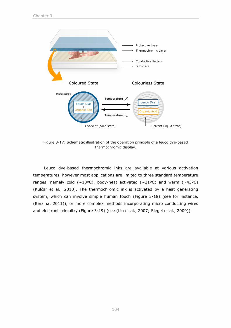
Chapter 3
104
Figure 3-17: Schematic illustration of the operation principle of a leuco dye-based
thermochromic display.
Leuco dye-based thermochromic inks are available at various activation
temperatures, however most applications are limited to three standard temperature
ranges, namely cold (~10ºC), body-heat activated (~31ºC) and warm (~43ºC)
(Kulčar et al., 2010). The thermochromic ink is activated by a heat generating
system, which can involve simple human touch (Figure 3-18) (see for instance,
(Berzina, 2011)), or more complex methods incorporating micro conducting wires
and electronic circuitry (Figure 3-19) (see (Liu et al., 2007; Siegel et al., 2009)).
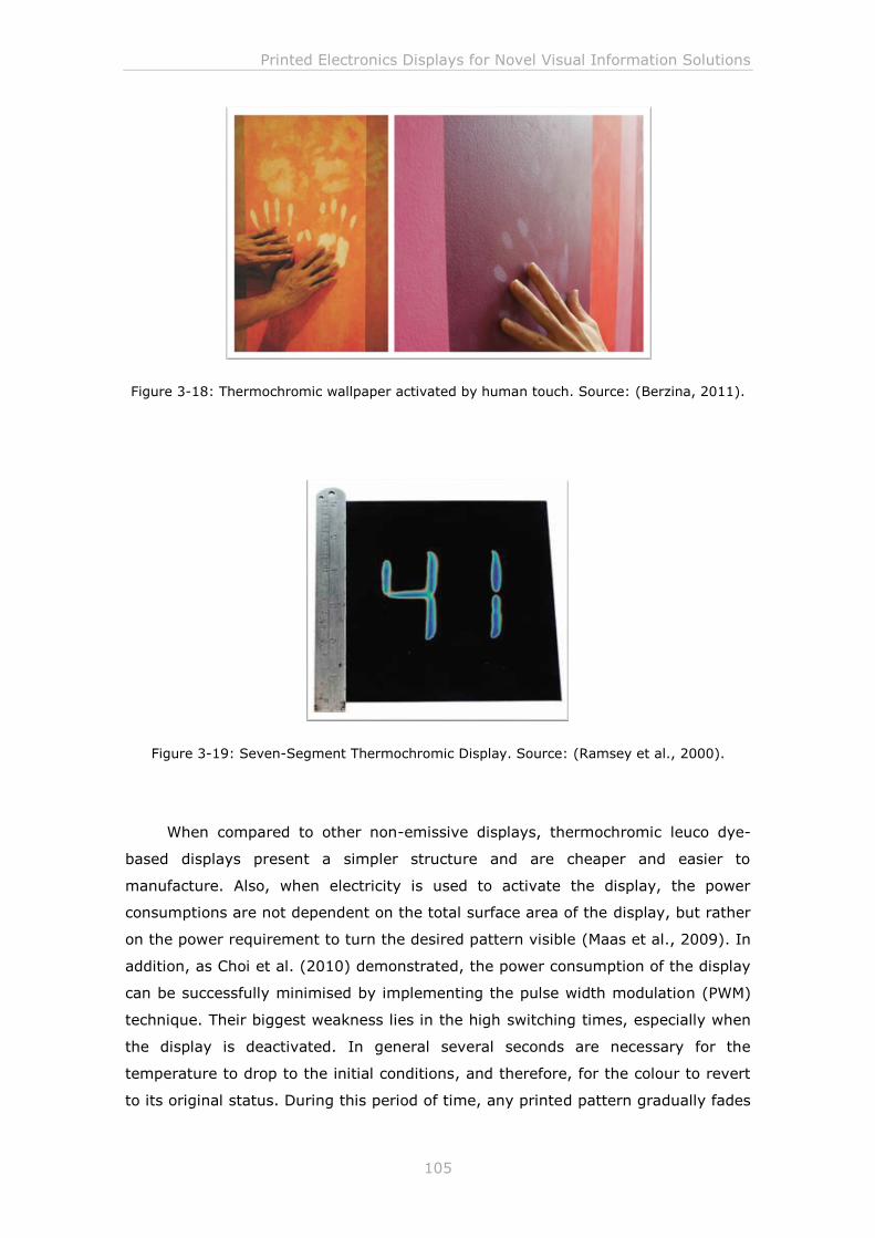
Printed Electronics Displays for Novel Visual Information Solutions
105
Figure 3-18: Thermochromic wallpaper activated by human touch. Source: (Berzina, 2011).
Figure 3-19: Seven-Segment Thermochromic Display. Source: (Ramsey et al., 2000).
When compared to other non-emissive displays, thermochromic leuco dye-
based displays present a simpler structure and are cheaper and easier to
manufacture. Also, when electricity is used to activate the display, the power
consumptions are not dependent on the total surface area of the display, but rather
on the power requirement to turn the desired pattern visible (Maas et al., 2009). In
addition, as Choi et al. (2010) demonstrated, the power consumption of the display
can be successfully minimised by implementing the pulse width modulation (PWM)
technique. Their biggest weakness lies in the high switching times, especially when
the display is deactivated. In general several seconds are necessary for the
temperature to drop to the initial conditions, and therefore, for the colour to revert
to its original status. During this period of time, any printed pattern gradually fades
Chapter 3
106
away. Hence, thermochromic displays are essentially appropriate for applications
that do not require frequent changes in the display content. There are several
parameters that can affect the switching times of thermochromic leuco dye-based
displays, namely, the voltage applied, the temperature of the ambience, the quality
of the paper, and, naturally, the activation temperature of the thermochromic ink
(Hennerdal and Berggren, 2011; Liu et al., 2007). For instance, by increasing the
voltage applied, faster switching times can be obtained, however, if the duration or
amount of the voltage applied is too much, the display can be overheated, leading
to blurred images.
Thermochromic displays are commonly used to produce dynamic colours in
products, such as mugs, t-shirts, magazines or toys; as temperature sensors when
the temperature response accuracy is not critical; as warning messages and safety
signs for products reaching certain temperatures; as security element for tickets,
smart cards or documents; or as temperature indicators implemented in packaging
products, such as beverages, ice-creams, or microwaveable products. Another good
example is the charge indicator on Duracell batteries. For more complex
applications, the implementation of specifically designed electronic circuitry, with
the aim to provide controlled and regulated temperature profiles to specific areas of
the display, enables the production of dynamic information, in opposite to
displaying only pre-programmed images. For instance, Glaister and co-workers
(Glaister et al., 2004) incorporated thermochromic materials into concrete, in
combination with a system of nickel-chromium wires connected to a power source,
in order to show low content information at the surface of the concrete. The
implementation of matrix addressing schemes, composed by thermal pixels, has
also been demonstrated (Yarimaga et al., 2010).
3.3 Technology comparison
This section attempts to highlight the main differences between the various
non-emissive display technologies previously addressed. In Table 3-1 it is provided
a side-by-side comparison between the different technologies based on key
performance factors. Both visual and operating performances are analysed, as well
as current state of maturity for each technology.
All the technologies considered are characterised for presenting paper-like
optics. They all possess a white state reflectivity higher than 40%19 and a contrast
19
Note that the surface of printed newspaper has a maximum reflectivity of 62% (Hattori et al., 2004).
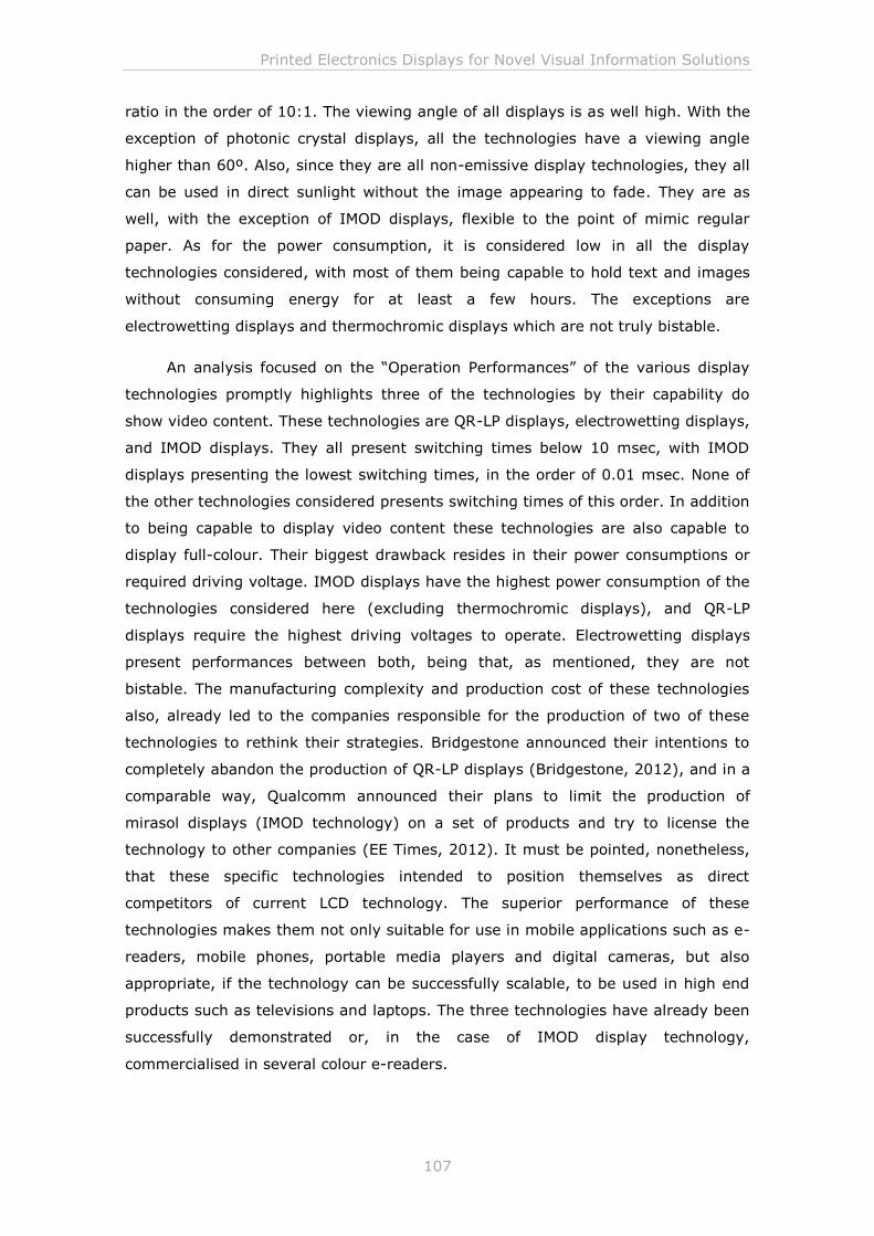
Printed Electronics Displays for Novel Visual Information Solutions
107
ratio in the order of 10:1. The viewing angle of all displays is as well high. With the
exception of photonic crystal displays, all the technologies have a viewing angle
higher than 60º. Also, since they are all non-emissive display technologies, they all
can be used in direct sunlight without the image appearing to fade. They are as
well, with the exception of IMOD displays, flexible to the point of mimic regular
paper. As for the power consumption, it is considered low in all the display
technologies considered, with most of them being capable to hold text and images
without consuming energy for at least a few hours. The exceptions are
electrowetting displays and thermochromic displays which are not truly bistable.
An analysis focused on the “Operation Performances” of the various display
technologies promptly highlights three of the technologies by their capability do
show video content. These technologies are QR-LP displays, electrowetting displays,
and IMOD displays. They all present switching times below 10 msec, with IMOD
displays presenting the lowest switching times, in the order of 0.01 msec. None of
the other technologies considered presents switching times of this order. In addition
to being capable to display video content these technologies are also capable to
display full-colour. Their biggest drawback resides in their power consumptions or
required driving voltage. IMOD displays have the highest power consumption of the
technologies considered here (excluding thermochromic displays), and QR-LP
displays require the highest driving voltages to operate. Electrowetting displays
present performances between both, being that, as mentioned, they are not
bistable. The manufacturing complexity and production cost of these technologies
also, already led to the companies responsible for the production of two of these
technologies to rethink their strategies. Bridgestone announced their intentions to
completely abandon the production of QR-LP displays (Bridgestone, 2012), and in a
comparable way, Qualcomm announced their plans to limit the production of
mirasol displays (IMOD technology) on a set of products and try to license the
technology to other companies (EE Times, 2012). It must be pointed, nonetheless,
that these specific technologies intended to position themselves as direct
competitors of current LCD technology. The superior performance of these
technologies makes them not only suitable for use in mobile applications such as e-
readers, mobile phones, portable media players and digital cameras, but also
appropriate, if the technology can be successfully scalable, to be used in high end
products such as televisions and laptops. The three technologies have already been
successfully demonstrated or, in the case of IMOD display technology,
commercialised in several colour e-readers.
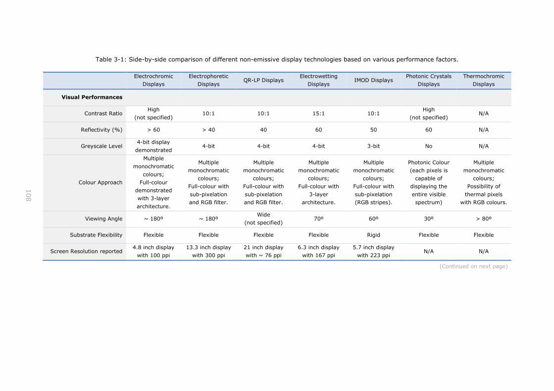
108
Table 3-1: Side-by-side comparison of different non-emissive display technologies based on various performance factors.
Electrochromic
Displays
Electrophoretic
Displays QR-LP Displays
Electrowetting
Displays IMOD Displays
Photonic Crystals
Displays
Thermochromic
Displays
Visual Performances
Contrast Ratio High
(not specified) 10:1 10:1 15:1 10:1
High
(not specified) N/A
Reflectivity (%) > 60 > 40 40 60 50 60 N/A
Greyscale Level 4-bit display
demonstrated 4-bit 4-bit 4-bit 3-bit No N/A
Colour Approach
Multiple
monochromatic
colours;
Full-colour
demonstrated
with 3-layer
architecture.
Multiple
monochromatic
colours;
Full-colour with
sub-pixelation
and RGB filter.
Multiple
monochromatic
colours;
Full-colour with
sub-pixelation
and RGB filter.
Multiple
monochromatic
colours;
Full-colour with
3-layer
architecture.
Multiple
monochromatic
colours;
Full-colour with
sub-pixelation
(RGB stripes).
Photonic Colour
(each pixels is
capable of
displaying the
entire visible
spectrum)
Multiple
monochromatic
colours;
Possibility of
thermal pixels
with RGB colours.
Viewing Angle ~ 180º ~ 180º Wide
(not specified) 70º 60º 30º > 80º
Substrate Flexibility Flexible Flexible Flexible Flexible Rigid Flexible Flexible
Screen Resolution reported 4.8 inch display
with 100 ppi
13.3 inch display
with 300 ppi
21 inch display
with ~ 76 ppi
6.3 inch display
with 167 ppi
5.7 inch display
with 223 ppi N/A N/A
(Continued on next page)
109
Electrochromic
Displays
Electrophoretic
Displays QR-LP Displays
Electrowetting
Displays IMOD Displays
Photonic Crystals
Displays
Thermochromic
Displays
Operation Performances
Driving Voltage (V) 1 to 5 15 40 to 70 15 to 20 ~ 10 < 1.5 5 to 15
Bistable Yes (~ 2 to 3 h) Yes Yes (months) No Yes (> 10 h) Yes (hours) No
Power Consumption (when
switching image) (mW/cm2) < 3 ~ 1.5 < 0.5 < 4.5 < 15.5
Low
(Not specified) ~ 50
Switching Time (msec) 100 to 1000 120 (up to 980 in
colour mode) 0.2 < 10 0.01 200 > 1000
Video Content No No Yes Yes Yes No No
Matrix Drive Passive-Matrix
Active-Matrix Active-Matrix Passive-Matrix Active-Matrix Passive-Matrix
PM / AM not
demonstrated
Active-Matrix
(thermal pixels)
Stage of Development
Demonstrated in
segmented and
matrix addressed
displays;
Commercialised
in products, such
as smart windows
or postcards.
Commercialised
in several
products, from e-
readers to
wristwatches.
Demonstrated in
segmented and
passive-matrix
displays
(e.g. e-readers
from Delta
Electronics).
Demonstrated in
several e-readers
prototypes.
Commercialised
in e-readers
(e.g. KYOBO e-
reader).
Demonstrated in
segmented
displays.
Commercialised
in several
products, from t-
shirts and mugs
to temperature
sensors and
security
elements.
References
(Chung et al.,
2010; Pettersson
et al., 2004;
Sonmez,
Sonmez, et al.,
2004; Yashiro et
al., 2011;
Ynvisible, 2012)
(Duthaler et al.,
2002; E Ink, n.d.,
n.d., n.d.;
Heikenfeld, 2011;
Pitt et al., 2002)
(Hattori et al.,
2004, 2005;
Masuda et al.,
2006; Sakurai et
al., 2006, 2007)
(Feenstra and
Hayes, 2009;
Feenstra, 2006;
Hayes et al.,
2004; Heikenfeld,
2011)
(Miles et al.,
2002; Qualcomm,
2008, 2013b)
(Opalux, 2013;
Wang et al.,
2011)
(Hennerdal and
Berggren, 2011;
Liu et al., 2007;
Siegel et al.,
2009)
Chapter 3
110
From all the display technologies considered, thermochromic displays (leuco
dye-based) are the ones that present the worst performances either in terms of
power consumption, required driving voltage, and switching time. Their main
attractiveness is mainly related to the easiness with which they can be
manufactured and the aptitude to directly created the display in almost any type of
substrate or product. This is the main reason why this type of technology is widely
used to produce dynamic colours in products, such as mugs, t-shirts, magazines or
toys. Nonetheless, this does not mean this type of technology can only be used for
this type of purpose. As already mentioned in section 3.2.7, thermochromic
displays can also be used as dynamic information displays in various applications,
from temperature indicators implemented in packaging products to segmented
displays embed in concrete.
The remaining three display technologies (electrochromic displays,
electrophoretic displays and photonic crystal displays) present similar operating
performances, although each one is at a different stage of maturity. The power
consumptions of the three technologies are relatively low, with electrophoretic
displays having the lowest power consumptions of the three. The driving voltages
are as well low, mainly in electrochromic and photonic crystals displays. Also, even
though these three technologies are not capable of showing video content, their
switching time can be as low as 200 msec. Electrophoretic display technology is
currently the technology with the best proven track record, even when compared to
the others technologies considered in this analyse. It is a well-established and well-
proven technology being commercialised in several products, from e-readers to
wristwatches, already for some years. Indeed an attractive choice for display
devices where video content is not relevant. Photonic crystal display technology, on
the other hand, is in its infancy. Until now, the technology has only been
demonstrated in single cell displays and segmented displays. Despite possessing
one of the most interesting features of all the display technologies highlighted here,
the ability to individually tune each picture element to a specific colour of the visible
spectrum, photonic crystal technology still requires considerable development in
order to become commercially viable. As for electrochromic displays, the
technology is being steadily studied since the early seventies and is currently used
in commercial products such as smart windows, rear-view mirrors, or greetings
postcards. Noteworthy that commercialisation is mainly focused on monochromatic
displays, with multiple colour or full-colour displays still in the lab stage. The
attractiveness of this technology resides essentially in the relation between the
visual and operation performances associated to a low production cost. As the
manufacturing process of electrochromic displays is relatively simple and relies
Printed Electronics Displays
111
essentially on common printing techniques, such as screen and inkjet printing, the
cost of production is largely reduced when compared to other display technologies.
These characteristics make this technology particularly suitable for use as
widespread low tech information displays. In sum, in applications where cost and
power consumption must be low, the switching speeds fast enough to allow quick
updates in the content of the displays but not necessarily fast to show video
content, and high visual performances are required but full-colour is not
fundamental (for instance, in electronic labels and electronic signage).
Paper is considered the display technology by excellence. It is being used
already for two millenniums and it still continues to have a fundamental role in the
presentation and divulgation of information. However, its content, by nature, is
static. Electrochromic displays, by mimicking certain properties of regular paper,
such as the look and agreeable readability, with the capacity to display dynamic
information can combine the best of the two realities and enable new forms for
users to consume information.
3.4 Concluding remarks
Visual information has an important role in today’s societies, being used
practically everywhere, from physical formats such as road signs and retail displays
to digital formats such as websites. The ability to transform traditionally passive
physical formats of visual information into active formats capable of presenting
information that is changeable and updatable in response to an external stimulus
opens new opportunities for presenting information. Inevitably, these displays will
have to have a low production cost, low power consumption, be flexible, lightweight
and robust, as well as viewable under various light conditions, including under
direct sunlight. This section provided an overview of currently emerging printed
non-emissive electronic display technologies. It described the technical
breakthroughs behind each type of technology, highlighting its advantages and
limitations. Furthermore, it presented existing and possible future applications.
The technologies reviewed allow the development of cheap, low power, ultra-
thin flexible displays with a high reflectivity and contrast. Due to these
characteristics, they bear the promise of revolutionising the display market. From
this review, it was possible to verify that non-emissive display technologies are
already competing for certain market areas with emissive displays and backlit liquid
crystal displays. This is particularly visible in low end electronic devices where non-
Chapter 3
112
emissive displays are starting to be seen as an economic and ecological alternative.
In the high end segment, considering that technologies such as plasma displays
and liquid crystal displays are reaching their economic limit in the size, constructors
are also starting to see non-emissive displays as an alternative. However, before
non-emissive electronic display technologies can be truly successful, some
improvements are still required. First, non-emissive electronic displays have to
become capable to display high resolution colours while maintaining the high
contrast and high reflectivity that characterize them. Secondly, non-emissive
electronic displays refresh rates have to be further improved to the point of
allowing fluid video content in large display devices. In the meantime, it expected
that non-emissive electronic displays will thrive in areas of advertising and smart
packaging, as well as in portable media applications. Nowadays, they already
dominate the electronic book readers market. Even so, the potential of these
displays is much greater. Their overall characteristics allow them to be incorporated
in various types of surfaces, enabling the fabrication of dynamic environments (for
example, in commercial spaces or health facilities), where visual information can be
accessed in a seamless way.
It must be pointed out nonetheless that none of the display technology
reviewed here meets all the technical requirements for every area of application.
Hence, it is unlikely that a specific technology will completely dominate all the
others in all possible market applications for displays. Instead, the dominance of
certain technologies will be more evident in certain application whilst in others they
will not thrive. Some technologies will simply be more suitable for certain
applications than others.
Electrochromic displays present some distinctive features particularly relevant
for the production of low cost, low power consumption display devices. The
structural simplicity of electrochromic displays and the easiness which they are
manufactured, together with the nature and availability of the raw materials used
to produce this type of displays, makes them very well suitable for mass production
as well as for Personal Fabrication. Indeed, the costs are expected to be low enough
to render them practical for single-use applications. In addition, the displays are
bistable and the average power consumptions are sufficiently low to enable their
operation with small batteries. Also, electrochromic displays can be manufactured
and assembled under normal environment conditions, not requiring special
installations. It is expected that these characteristics will greatly contribute to the
incorporation of electrochromic displays into all kind of objects, creating new
products and new ways to experience and interact with digital information.
Printed Electronics Displays
113
Nonetheless, electrochromic displays still need some improvements. For instance, it
is necessary to overcome the long-term degradation of the electrochromic displays
and thus, increase its lifetime. As Heikenfeld et al. (2011) point out, there is still a
sizable gap between the theoretical performance of electrochromic displays and the
actual capabilities of working displays.

Chapter 3
114
System Architecture: Assembling Printed Electronics Visual Information Applications
115
4 System Architecture: Assembling Printed
Electronics Visual Information Applications
4.1 Hardware Structure
One of the main concerns when developing the hardware structure for the
various devices was to keep the hardware components to a minimum necessary.
Several hardware structures were explored depending on the desired visual content
and are here systematised. The assembly of the devices was done following an
approach that intended to combine the principles behind Printed Electronics and
Personal Fabrication. In the following subsections is explained in detail the
assembly process, namely of direct addressing, passive-matrix and active-matrix
electrochromic displays as well as of the required control units.
4.1.1 Display assembly
Electrochromic displays, as mention in section 3.2.1, are typically composed
of five superimposed layers positioned between two protective substrates in a
laminate configuration. The electrochromic layer and the electroactive layer are
physically separated from each other by a solid, semi-solid or liquid electrolyte, and
stacked between two opposing electrodes. The devices produced in the context of
this thesis were assembled according to the following configuration, in normal
ambient conditions (Figure 4-1):
⟨ ( 𝑃𝐸𝑇 | 𝐼𝑇𝑂) | 𝑃𝐸𝐷𝑂𝑇: 𝑃𝑆𝑆 | | 𝐸𝑙𝑒𝑐𝑡𝑟𝑜𝑙𝑦𝑡𝑒 | | 𝑃𝐸𝐷𝑂𝑇: 𝑃𝑆𝑆 | ( 𝐼𝑇𝑂 | 𝑃𝐸𝑇 ) ⟩
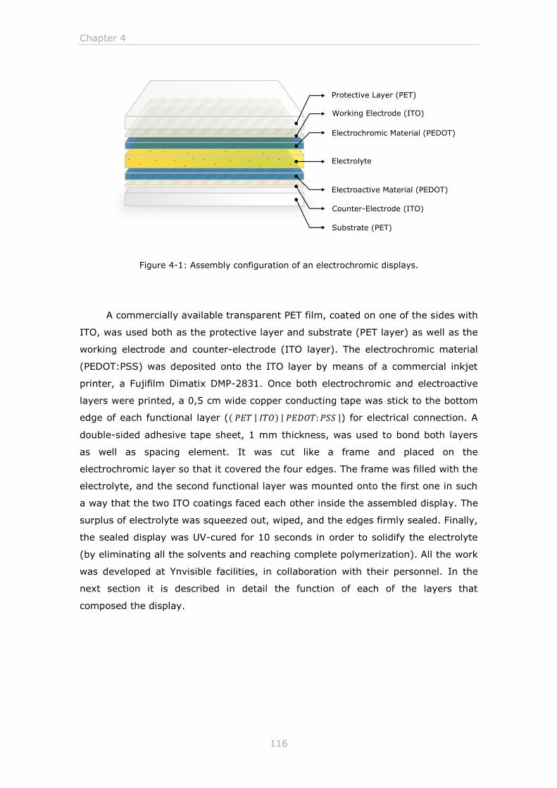
Chapter 4
116
Figure 4-1: Assembly configuration of an electrochromic displays.
A commercially available transparent PET film, coated on one of the sides with
ITO, was used both as the protective layer and substrate (PET layer) as well as the
working electrode and counter-electrode (ITO layer). The electrochromic material
(PEDOT:PSS) was deposited onto the ITO layer by means of a commercial inkjet
printer, a Fujifilm Dimatix DMP-2831. Once both electrochromic and electroactive
layers were printed, a 0,5 cm wide copper conducting tape was stick to the bottom
edge of each functional layer (( 𝑃𝐸𝑇 | 𝐼𝑇𝑂) | 𝑃𝐸𝐷𝑂𝑇: 𝑃𝑆𝑆 |) for electrical connection. A
double-sided adhesive tape sheet, 1 mm thickness, was used to bond both layers
as well as spacing element. It was cut like a frame and placed on the
electrochromic layer so that it covered the four edges. The frame was filled with the
electrolyte, and the second functional layer was mounted onto the first one in such
a way that the two ITO coatings faced each other inside the assembled display. The
surplus of electrolyte was squeezed out, wiped, and the edges firmly sealed. Finally,
the sealed display was UV-cured for 10 seconds in order to solidify the electrolyte
(by eliminating all the solvents and reaching complete polymerization). All the work
was developed at Ynvisible facilities, in collaboration with their personnel. In the
next section it is described in detail the function of each of the layers that
composed the display.
System Architecture: Assembling Printed Electronics Visual Information Applications
117
4.1.1.1 Display components
4.1.1.1.1 Electrochromic and electroactive layers
Electrochromic devices can be regarded as a rechargeable electrochemical
cell, where half-cell is in part composed by the electrochromic layer and the other
half by the electroactive layer. When an electric field is applied to the
electrochromic layer, it becomes absorptive to the electromagnetic radiation of a
certain wavelength in the visible region. As a result, it becomes coloured. In turn,
when the application of the electric field ceases, the electrochromic material
changes back to its initial redox state along with its optical absorptions. Typically,
this change is to a non-absorbent state in the visible spectrum, resulting in the
electrochromic layer becoming transparent. In the case that both electrochromic
states are absorptive in the visible spectrum, the electrochromic layer switches to
another distinct colour. The complete oxidation or reduction of the electrochromic
layer results in the greatest amount of optical contrast possible.
The main purpose of the electroactive layer is to counter balance the charges
of the electrochromic layer upon the redox reaction. Nonetheless, the electroactive
layer can also be electrochromic. In these cases, the colouration of the electroactive
layer is induced when charging the electrochromic layer with an opposite charge of
that of the electroactive layer. Hence, when an electrochromic reaction such as an
electrochemical oxidation occurs at the electrochromic layer, a reduction reaction
involving the same amount of charge transfer as in the oxidation reaction occurs at
the electroactive layer (the electron transference is done in the reverse sense of
that of the electrochromic layer).
The electrochromic material used as the electroactive layer can be the same
as the one of the persistent electrochromic layer or different. The use of the same
electrochromic material in both layers facilitates the assembly process, limiting
however the number of possible colours. The superimposition of the two layers can
be used to create, for instance, two complementary images that, depending on the
electrochromic materials chosen, can have distinct colours. To successfully observe
the colours transitions, both layers need to have a colourless transparent
electrochromic mode.
Several chemical materials, both inorganic and organic, are known to show
electrochromic behaviour and have been extensively investigated and reviewed on
various publications covering the diverse categories of electrochromic materials and
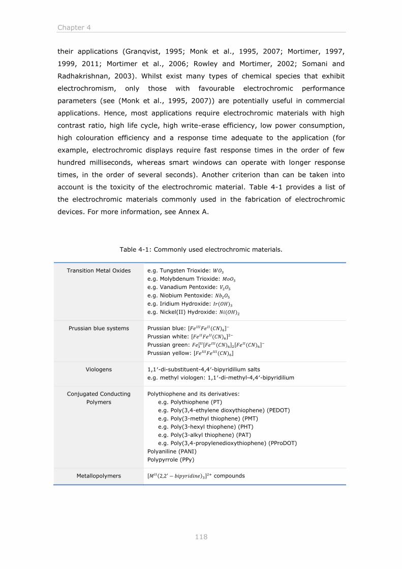
Chapter 4
118
their applications (Granqvist, 1995; Monk et al., 1995, 2007; Mortimer, 1997,
1999, 2011; Mortimer et al., 2006; Rowley and Mortimer, 2002; Somani and
Radhakrishnan, 2003). Whilst exist many types of chemical species that exhibit
electrochromism, only those with favourable electrochromic performance
parameters (see (Monk et al., 1995, 2007)) are potentially useful in commercial
applications. Hence, most applications require electrochromic materials with high
contrast ratio, high life cycle, high write-erase efficiency, low power consumption,
high colouration efficiency and a response time adequate to the application (for
example, electrochromic displays require fast response times in the order of few
hundred milliseconds, whereas smart windows can operate with longer response
times, in the order of several seconds). Another criterion than can be taken into
account is the toxicity of the electrochromic material. Table 4-1 provides a list of
the electrochromic materials commonly used in the fabrication of electrochromic
devices. For more information, see Annex A.
Table 4-1: Commonly used electrochromic materials.
Transition Metal Oxides e.g. Tungsten Trioxide: 𝑊𝑂3
e.g. Molybdenum Trioxide: 𝑀𝑜𝑂3
e.g. Vanadium Pentoxide: 𝑉2𝑂5
e.g. Niobium Pentoxide: 𝑁𝑏2𝑂5
e.g. Iridium Hydroxide: 𝐼𝑟(𝑂𝐻)3
e.g. Nickel(II) Hydroxide: 𝑁𝑖(𝑂𝐻)2
Prussian blue systems Prussian blue: [𝐹𝑒𝐼𝐼𝐼𝐹𝑒𝐼𝐼(𝐶𝑁)6]−
Prussian white: [𝐹𝑒𝐼𝐼𝐹𝑒𝐼𝐼(𝐶𝑁)6]2−
Prussian green: 𝐹𝑒3𝐼𝐼𝐼[𝐹𝑒𝐼𝐼𝐼(𝐶𝑁)6]2[𝐹𝑒𝐼𝐼(𝐶𝑁)6]−
Prussian yellow: [𝐹𝑒𝐼𝐼𝐼𝐹𝑒𝐼𝐼𝐼(𝐶𝑁)6]
Viologens 1,1′-di-substituent-4,4′-bipyridilium salts
e.g. methyl viologen: 1,1′-di-methyl-4,4′-bipyridilium
Conjugated Conducting
Polymers
Polythiophene and its derivatives:
e.g. Polythiophene (PT)
e.g. Poly(3,4-ethylene dioxythiophene) (PEDOT)
e.g. Poly(3-methyl thiophene) (PMT)
e.g. Poly(3-hexyl thiophene) (PHT)
e.g. Poly(3-alkyl thiophene) (PAT)
e.g. Poly(3,4-propylenedioxythiophene) (PProDOT)
Polyaniline (PANI)
Polypyrrole (PPy)
Metallopolymers [𝑀𝐼𝐼(2,2′ − 𝑏𝑖𝑝𝑦𝑟𝑖𝑑𝑖𝑛𝑒)3]2+ compounds
System Architecture: Assembling Printed Electronics Visual Information Applications
119
The electrochromic displays produced in the context of this thesis all used
PEDOT:PSS as the electrochromic material20. The thin films were prepared from a
commercially available solution of PEDOT:PSS from Aldrich Chemistry (reference
483095), kindly supplied by Ynvisible. The deposition of the PEDOT:PSS film was
done by means of a commercial inkjet printer (Fujifilm Dimatix DMP-2831)21, at
Ynvisible facilities. The choice of PEDOT:PSS as the electrochromic material was
mainly because of its properties, in particular, its high chemical stability in normal
conditions; its high optical contrast between the bleached and coloured state; and
its low electronic bandgap; as well as due to the fact that it can be processed from
a water emulsion and easily deposited in various substrate, rigid and flexible, by
means of inkjet printing.
4.1.1.1.2 Ion-conducting layer: electrolyte
The electrolyte physically separates the electrochromic layer from the
electroactive layer and thus, the working electrode from the counter-electrode.
However, beyond functioning merely as a physical separator, the electrolyte layer is
primarily an ion-storage layer, acting as a source and sink of cations and anions as
the various redox processes take place. It is through the electrolyte layer that
charged species are exchanged between the electrochromic and the electroactive
layers during the redox process, and that the same process is balanced. As
electrons are injected in one of the electrodes, the equivalent amount of electrons
is extracted from the other. Eventually, the continuous flow of electrons results in
the electrochromic cell becoming polarised. The ions present in the electrolyte layer
counteract the polarisation by electrically neutralising the surplus of charges in the
electrodes. To avoid short circuits in the electrochromic cell, both electrodes must
be physically and electrically separated. Hence, the electrolyte layer must be not
only ionically conductive but also an electrical insulator. The electrolyte layer has to
be as well highly transparent and electrochemically inert over the voltage potential
range needed to induce the colour transition, i.e. it cannot participate in the
electrochemical reactions.
The electrolyte typically consists of a salt dissolved in a polymer matrix (see
for instance, (Gray, 1991; MacCallum and Vincent, 1989)). The salt is responsible
for the introduction of positive or negative charge carriers, and the polymer matrix
serves as the medium through which they move between the polarised electrodes.
20 See Box A-1 in Annex A for more information about PEDOT. 21 See (Fujifilm Dimatix, 2008) for the printer datasheet.
Chapter 4
120
The viscosity of such polymers increases with molecular weight, hence polymers
range from liquid at low molecular weight to longer polymers that behave as rigid
solids (Byker, 2001; Mortimer, 2011). As such, several types of electrolytes have
been developed and used in electrochromic devices including liquid (Huang and Ho,
2006; Randin, 1978; Rocco et al., 1996; Schmitt and Aegerter, 2001), gel (Inaba
et al., 1995; Kobayashi et al., 2007; Su et al., 1998; Vondrák et al., 1999), solid
(De Paoli et al., 1997; Duek et al., 1993; Jee et al., 2011; Varshney et al., 2003),
hybrid (Liang and Kuo, 2004; Orel et al., 2003; Rodrigues et al., 2011; Souza et
al., 2007; Zelazowska et al., 2007) and ionic liquid (Brazier et al., 2007; Desai et
al., 2011; Lu et al., 2002, 2003; Marcilla et al., 2006; Vidinha et al., 2008)
electrolytes. The selection of an appropriate electrolyte system is fundamental in
terms of operation and long term stability of the electrochromic device. Frequent
stability problems associated with electrolytes include solvent volatility and
electrolyte leakage. These typically arise from mechanical seal failures and
ultimately result in the device failure. For more information on the various types of
electrolytes, see Annex B.
4.1.1.1.3 Working electrode and counter-electrode
The working electrode and the counter-electrode are typically formed by an
optically transparent, electrically conducting transition-metal oxide thin film. Indium
tin oxide (tin-doped indium oxide or simply, ITO) (see (Ishiguro et al., 1958)) is
currently the industry standard. The low electrical resistance and the high
transmittance in the visible region of the electromagnetic spectrum, as well as the
chemical resistance and the ease with which can be deposited as a thin film make
ITO the transparent conducting film of choice, being widely used as electrode in
most known flat panel display technologies, namely in liquid crystal displays,
plasma displays, light-emitting diode (LED) displays, and electronic ink based
displays, apart from electrochromic displays. As with all transparent conducting
films, a compromise must be made between the conductivity and the transparency
of the thin film. By decreasing the thickness of the film it is possible to improve its
transparency, however, this will consequently result in a decrease of the
concentration of charge carriers and thus in a reduction of the film conductivity. ITO
thin films are commonly deposited on surfaces by electron beam evaporation,
physical vapour deposition, or a range of sputter deposition techniques.
Despite the attractive properties, the use of ITO as the choice material in
these applications may be limited for both technical and economic reasons. The
System Architecture: Assembling Printed Electronics Visual Information Applications
121
limited supply of indium, and its consequent high cost, along with the ever-
increasing number of devices requiring flat panel displays, started to contest the
viability of using such a rare element for transparent conducting films.
Furthermore, ITO is a brittle, crystalline material that when stressed can fracture,
irreversibly dropping the film conductivity by several orders of magnitude and thus
limiting its utility in applications that require some flexibility. Hence, alternatives
are in high demand (Demming, 2012; Wassei and Kaner, 2010). Novel alternatives
include the use of organic films developed using carbon nanotubes (Nakayama and
Akita, 2001; Wu et al., 2004; Zhang et al., 2006) or graphene (Lahiri et al., 2011;
Wang et al., 2010; Wassei and Kaner, 2010), as well as conductive polymers such
as PEDOT and its derivatives (Y-B Kim et al., 2009; Wang and MacDiarmid, 2007),
or thin foils of silver (De et al., 2009; Zeng et al., 2010) or copper (Kang et al.,
2010; Rathmell et al., 2010) nanowires.
The optically transparent electrodes are typically coated on a transparent
substrate such as glass or plastic, although other materials like paper, wood,
ceramic, or cork, with different optical properties, can also be used. It must be
noted, nonetheless, that at least one of the electrodes has to be transparent.
4.1.1.1.4 Protective layer and substrate
Practical applications of electrochromic devices require that these be able to
resist the adverse conditions of the environment in addition to withstand everyday
physical use. The exposure to atmospheric oxygen and water, as well as to other
environmental contaminates such as ammonia, chlorine, or hydrogen sulphide, can
degrade the performance of electrochromic devices and reduce their lifetime.
Hence, electrochromic devices must be built not only to prevent internal materials
from escaping the device, but also to prevent external materials from entering. The
protective layer and the substrate provide the required barrier against the
deleterious effects of ambient oxidants as well as protection against mechanical
damage, in addition to function as a support structure for the different components
of the electrochromic device. The sealant used around the electrochromic device
must also withstand the adverse environmental conditions and be chemically
stable.
Traditionally, the protective layer and substrate consist of a laminate glass
pane which can be heat-strengthened or tempered, or of a plastic film, such as
polyethylene terephthalate (PET). Glass has been widely used mainly because of its
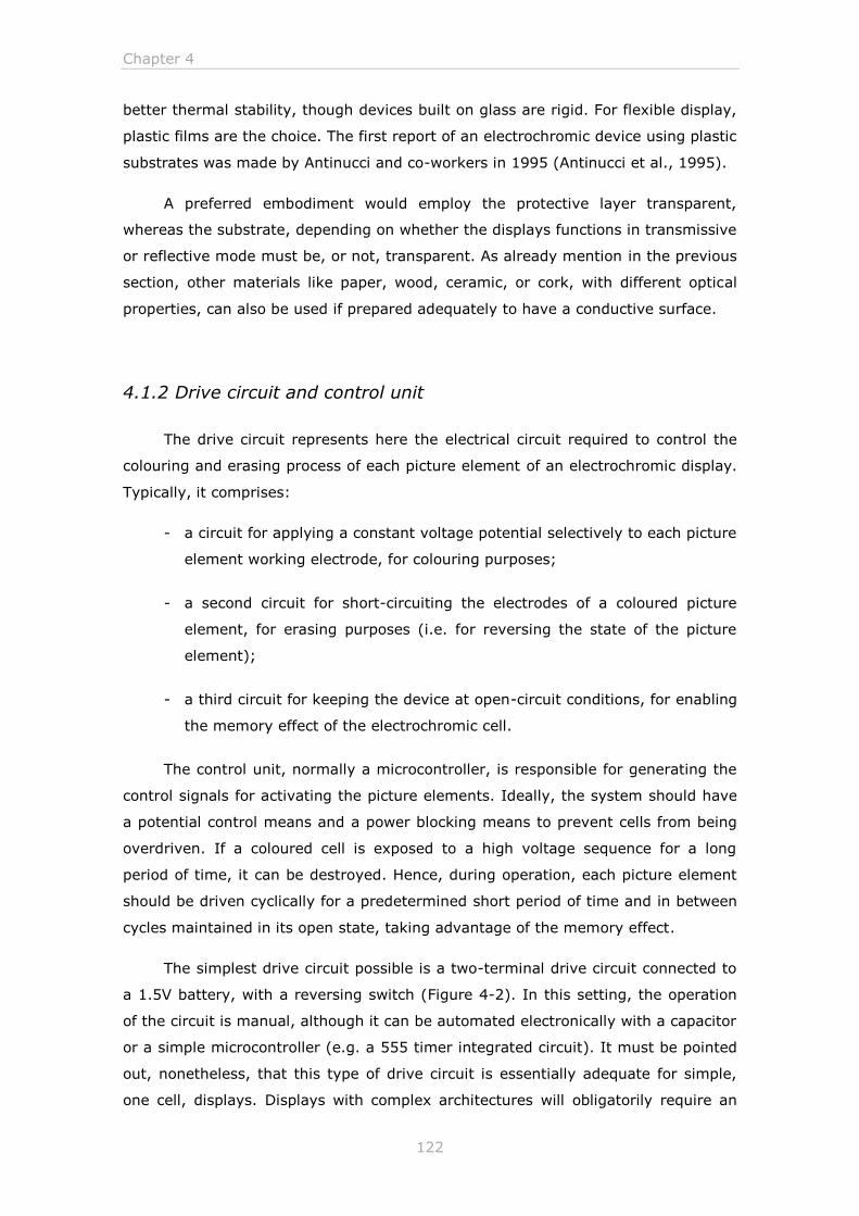
Chapter 4
122
better thermal stability, though devices built on glass are rigid. For flexible display,
plastic films are the choice. The first report of an electrochromic device using plastic
substrates was made by Antinucci and co-workers in 1995 (Antinucci et al., 1995).
A preferred embodiment would employ the protective layer transparent,
whereas the substrate, depending on whether the displays functions in transmissive
or reflective mode must be, or not, transparent. As already mention in the previous
section, other materials like paper, wood, ceramic, or cork, with different optical
properties, can also be used if prepared adequately to have a conductive surface.
4.1.2 Drive circuit and control unit
The drive circuit represents here the electrical circuit required to control the
colouring and erasing process of each picture element of an electrochromic display.
Typically, it comprises:
- a circuit for applying a constant voltage potential selectively to each picture
element working electrode, for colouring purposes;
- a second circuit for short-circuiting the electrodes of a coloured picture
element, for erasing purposes (i.e. for reversing the state of the picture
element);
- a third circuit for keeping the device at open-circuit conditions, for enabling
the memory effect of the electrochromic cell.
The control unit, normally a microcontroller, is responsible for generating the
control signals for activating the picture elements. Ideally, the system should have
a potential control means and a power blocking means to prevent cells from being
overdriven. If a coloured cell is exposed to a high voltage sequence for a long
period of time, it can be destroyed. Hence, during operation, each picture element
should be driven cyclically for a predetermined short period of time and in between
cycles maintained in its open state, taking advantage of the memory effect.
The simplest drive circuit possible is a two-terminal drive circuit connected to
a 1.5V battery, with a reversing switch (Figure 4-2). In this setting, the operation
of the circuit is manual, although it can be automated electronically with a capacitor
or a simple microcontroller (e.g. a 555 timer integrated circuit). It must be pointed
out, nonetheless, that this type of drive circuit is essentially adequate for simple,
one cell, displays. Displays with complex architectures will obligatorily require an
System Architecture: Assembling Printed Electronics Visual Information Applications
123
adequate control unit to manage the state of the various picture elements that
compose the display.
Figure 4-2: Schematic representation of a drive circuit for a simple electrochromic display
controlled by a toggle button.
The initial electrochromic display prototypes developed by the author when
exploring the various addressing schemes possible (see next chapter) had as a
control unit an adapted Arduino Mega board22. The main rationale behind this
approach was to use an open-source platform that could be easily purchasable and
easily programmable by anyone.
4.1.2.1 Addressing methods
Addressing can be defined as the process by which individual picture elements
in a display (generally pixels) are switched on or off in order to create an image on
the display. There are three main different addressing methods by which this can
be done: direct addressing, passive-matrix addressing and active-matrix addressing
(Cristaldi et al., 2009; Kelly and O’Neill, 2000). The implementation of a particular
addressing method in an electrochromic display is closely related to its desired
application, the information content to be displayed and the production cost. The
display area and the response time can also have influence in the choice, however,
generally are not decisive. The selection of one method over other influences the
architecture and construction of the display, as the operation of the microcontroller
responsible for controlling the display.
22 Arduino is an open-source electronics prototyping platform based on easy-to-use hardware and
software. The hardware consists of a small microcontroller board, commonly known as Arduino board, set up with an Atmel AVR processor and on-board input/output (I/O) support. The software consists of a standard programming language compiler known as the Arduino IDE (Integrated Development Environment), used to program the Atmel AVR processor. The Arduino boards can be easily purchased online or in any electronics store and they are used by hobbyists and makers everywhere in the word. For more information on the Arduino open-source platform, see (Banzi, 2011; Margolis, 2011).
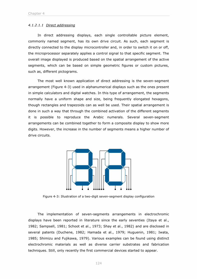
Chapter 4
124
4.1.2.1.1 Direct addressing
In direct addressing displays, each single controllable picture element,
commonly named segment, has its own drive circuit. As such, each segment is
directly connected to the display microcontroller and, in order to switch it on or off,
the microprocessor separately applies a control signal to that specific segment. The
overall image displayed is produced based on the spatial arrangement of the active
segments, which can be based on simple geometric figures or custom pictures,
such as, different pictograms.
The most well known application of direct addressing is the seven-segment
arrangement (Figure 4-3) used in alphanumerical displays such as the ones present
in simple calculators and digital watches. In this type of arrangement, the segments
normally have a uniform shape and size, being frequently elongated hexagons,
though rectangles and trapezoids can as well be used. Their spatial arrangement is
done in such a way that through the combined activation of the different segments
it is possible to reproduce the Arabic numerals. Several seven-segment
arrangements can be combined together to form a composite display to show more
digits. However, the increase in the number of segments means a higher number of
drive circuits.
Figure 4-3: Illustration of a two-digit seven-segment display configuration
The implementation of seven-segments arrangements in electrochromic
displays have been reported in literature since the early seventies (Itaya et al.,
1982; Sampsell, 1981; Schoot et al., 1973; Shay et al., 1982) and are disclosed in
several patents (Duchene, 1982; Hamada et al., 1979; Huguenin, 1981; Iwata,
1985; Shimizu and Fujikawa, 1979). Various examples can be found using distinct
electrochromic materials as well as diverse carrier substrates and fabrication
techniques. Still, only recently the first commercial devices started to appear.
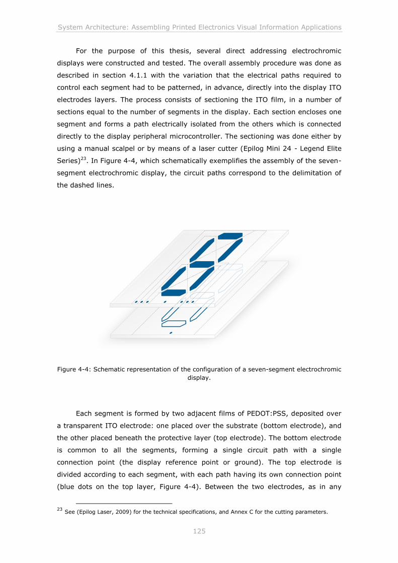
System Architecture: Assembling Printed Electronics Visual Information Applications
125
For the purpose of this thesis, several direct addressing electrochromic
displays were constructed and tested. The overall assembly procedure was done as
described in section 4.1.1 with the variation that the electrical paths required to
control each segment had to be patterned, in advance, directly into the display ITO
electrodes layers. The process consists of sectioning the ITO film, in a number of
sections equal to the number of segments in the display. Each section encloses one
segment and forms a path electrically isolated from the others which is connected
directly to the display peripheral microcontroller. The sectioning was done either by
using a manual scalpel or by means of a laser cutter (Epilog Mini 24 - Legend Elite
Series)23. In Figure 4-4, which schematically exemplifies the assembly of the seven-
segment electrochromic display, the circuit paths correspond to the delimitation of
the dashed lines.
Figure 4-4: Schematic representation of the configuration of a seven-segment electrochromic
display.
Each segment is formed by two adjacent films of PEDOT:PSS, deposited over
a transparent ITO electrode: one placed over the substrate (bottom electrode), and
the other placed beneath the protective layer (top electrode). The bottom electrode
is common to all the segments, forming a single circuit path with a single
connection point (the display reference point or ground). The top electrode is
divided according to each segment, with each path having its own connection point
(blue dots on the top layer, Figure 4-4). Between the two electrodes, as in any
23 See (Epilog Laser, 2009) for the technical specifications, and Annex C for the cutting parameters.
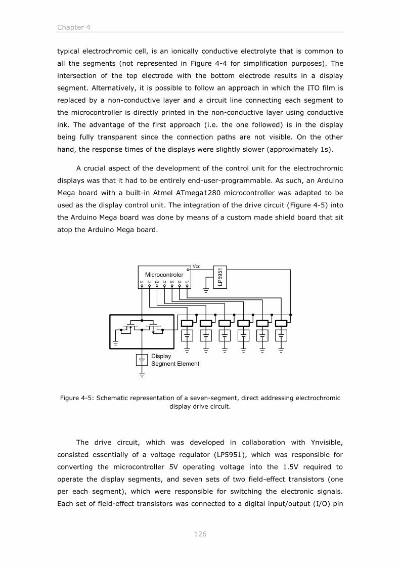
Chapter 4
126
typical electrochromic cell, is an ionically conductive electrolyte that is common to
all the segments (not represented in Figure 4-4 for simplification purposes). The
intersection of the top electrode with the bottom electrode results in a display
segment. Alternatively, it is possible to follow an approach in which the ITO film is
replaced by a non-conductive layer and a circuit line connecting each segment to
the microcontroller is directly printed in the non-conductive layer using conductive
ink. The advantage of the first approach (i.e. the one followed) is in the display
being fully transparent since the connection paths are not visible. On the other
hand, the response times of the displays were slightly slower (approximately 1s).
A crucial aspect of the development of the control unit for the electrochromic
displays was that it had to be entirely end-user-programmable. As such, an Arduino
Mega board with a built-in Atmel ATmega1280 microcontroller was adapted to be
used as the display control unit. The integration of the drive circuit (Figure 4-5) into
the Arduino Mega board was done by means of a custom made shield board that sit
atop the Arduino Mega board.
Figure 4-5: Schematic representation of a seven-segment, direct addressing electrochromic
display drive circuit.
The drive circuit, which was developed in collaboration with Ynvisible,
consisted essentially of a voltage regulator (LP5951), which was responsible for
converting the microcontroller 5V operating voltage into the 1.5V required to
operate the display segments, and seven sets of two field-effect transistors (one
per each segment), which were responsible for switching the electronic signals.
Each set of field-effect transistors was connected to a digital input/output (I/O) pin
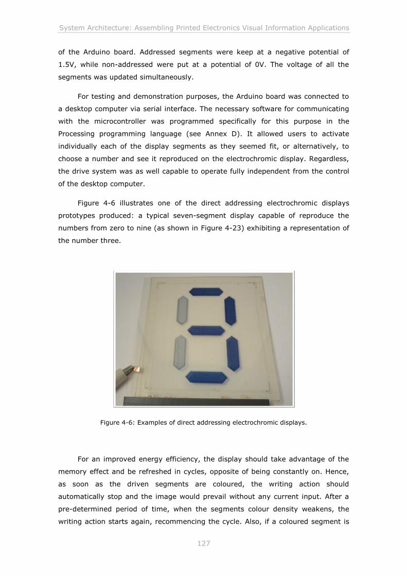
System Architecture: Assembling Printed Electronics Visual Information Applications
127
of the Arduino board. Addressed segments were keep at a negative potential of
1.5V, while non-addressed were put at a potential of 0V. The voltage of all the
segments was updated simultaneously.
For testing and demonstration purposes, the Arduino board was connected to
a desktop computer via serial interface. The necessary software for communicating
with the microcontroller was programmed specifically for this purpose in the
Processing programming language (see Annex D). It allowed users to activate
individually each of the display segments as they seemed fit, or alternatively, to
choose a number and see it reproduced on the electrochromic display. Regardless,
the drive system was as well capable to operate fully independent from the control
of the desktop computer.
Figure 4-6 illustrates one of the direct addressing electrochromic displays
prototypes produced: a typical seven-segment display capable of reproduce the
numbers from zero to nine (as shown in Figure 4-23) exhibiting a representation of
the number three.
Figure 4-6: Examples of direct addressing electrochromic displays.
For an improved energy efficiency, the display should take advantage of the
memory effect and be refreshed in cycles, opposite of being constantly on. Hence,
as soon as the driven segments are coloured, the writing action should
automatically stop and the image would prevail without any current input. After a
pre-determined period of time, when the segments colour density weakens, the
writing action starts again, recommencing the cycle. Also, if a coloured segment is
Chapter 4
128
exposed for too long to a high voltage, or alternatively to an excessive voltage, the
segment will be overdriven and, eventually, visually damaged.
Display format, response time, and contrast are all features that can vary
depending on the desired use. Factors such as the size of the segments, and for
that matter of the display, the ohmic resistance between segments and connection
points, as well as the applied voltage strongly influence the response time. Higher
colour contrasts and image contrasts can be achieved by printing additional layers
of electrochromic material or by using a versatile driver that allows the control of
the signal amplitude individually for each pixel. Because colouration in
electrochromic devices is an electrochromic reaction, colour density is proportional
to the quantity of electricity flowing in the display electrode per square area. If too
many segments are driven simultaneously at an equal voltage for an equal period
of time, each segment can have a different colour density depending on the size of
the segment or on the number of segments that are driven simultaneously. Possible
solutions include adjusting the output impedance of each driving circuit in
proportion to the number of simultaneously driven segments, as well as in
accordance to the segments areas, or using different driving times for each
segment.
Overall, direct addressing is essentially convenient for display applications
where there are only a reduced number of elements that have to be activated. A
display with n segments requires a total of n drivers with n+1 connections (one for
each segment, in addition to one for the reference point). Increasing the number of
segments to further increase the information content of the display can significantly
raise the number of connections to a point where managing all becomes too
complicated. For example, if we consider a typical seven-segment display, to
replicate a simple digital clock with six digits, using a direct addressing approach, a
minimum number of 42+1 connections are required. However, if the display must
be able as well to display text, a fourteen-segment scheme must be implemented
(at least), raising the number of connections to 84+1. It is possible to partially
diminish this problem by using a multiplexed approach, where the anodes of
equivalent segments of different digits are connected together and to a single
driver, while the cathodes of all segments for each digit would be connected
separately. In this way, a six digit display with seven segments would require only
6 cathode drivers and 6 anode drivers. This approach requires, nonetheless, that
each single digit be operated sequentially: to activate a certain number of
segments on a particular digit, the cathode driver for the selected digit and the
anode drivers for the desired segments have to be enabled. In order then to
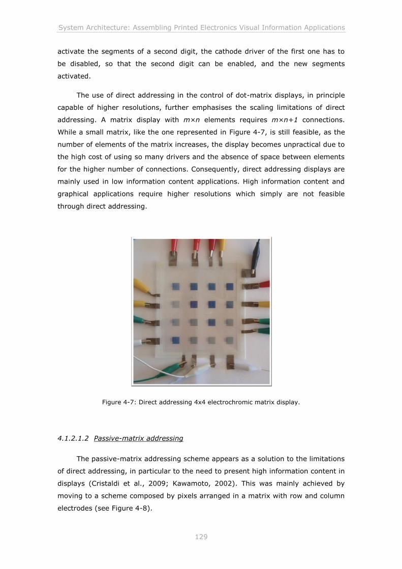
System Architecture: Assembling Printed Electronics Visual Information Applications
129
activate the segments of a second digit, the cathode driver of the first one has to
be disabled, so that the second digit can be enabled, and the new segments
activated.
The use of direct addressing in the control of dot-matrix displays, in principle
capable of higher resolutions, further emphasises the scaling limitations of direct
addressing. A matrix display with m×n elements requires m×n+1 connections.
While a small matrix, like the one represented in Figure 4-7, is still feasible, as the
number of elements of the matrix increases, the display becomes unpractical due to
the high cost of using so many drivers and the absence of space between elements
for the higher number of connections. Consequently, direct addressing displays are
mainly used in low information content applications. High information content and
graphical applications require higher resolutions which simply are not feasible
through direct addressing.
Figure 4-7: Direct addressing 4x4 electrochromic matrix display.
4.1.2.1.2 Passive-matrix addressing
The passive-matrix addressing scheme appears as a solution to the limitations
of direct addressing, in particular to the need to present high information content in
displays (Cristaldi et al., 2009; Kawamoto, 2002). This was mainly achieved by
moving to a scheme composed by pixels arranged in a matrix with row and column
electrodes (see Figure 4-8).
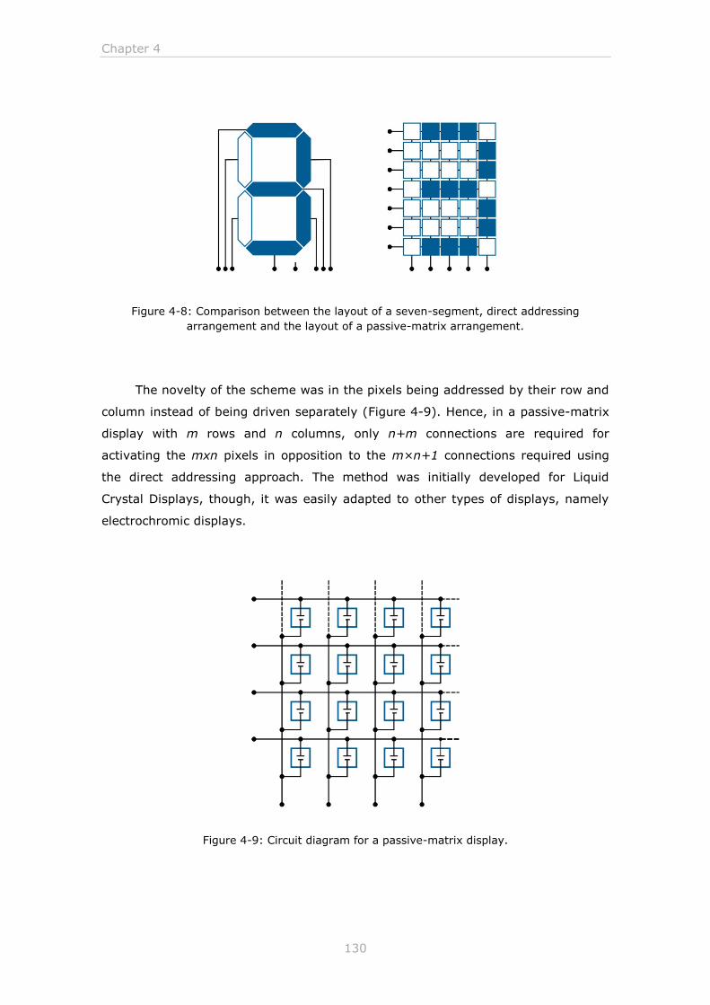
Chapter 4
130
Figure 4-8: Comparison between the layout of a seven-segment, direct addressing
arrangement and the layout of a passive-matrix arrangement.
The novelty of the scheme was in the pixels being addressed by their row and
column instead of being driven separately (Figure 4-9). Hence, in a passive-matrix
display with m rows and n columns, only n+m connections are required for
activating the mxn pixels in opposition to the m×n+1 connections required using
the direct addressing approach. The method was initially developed for Liquid
Crystal Displays, though, it was easily adapted to other types of displays, namely
electrochromic displays.
Figure 4-9: Circuit diagram for a passive-matrix display.
System Architecture: Assembling Printed Electronics Visual Information Applications
131
To activate a specific pixel in a passive-matrix display, a carefully timed
control signal is sent across the row containing the selected pixel, while the
corresponding column is connected to ground. By applying the control signals
sequentially, row by row, each individual pixel within the entire display matrix can
be uniquely addressed. An external microcontroller is responsible for controlling
where and when the control signals are applied. For the method to function, each
pixel in a passive-matrix display has to be capable of maintain its state without
active circuitry until it can be refreshed again, i.e. it has to be bi-stable. If the
refresh time of the entire display is shorter than the turn-off time, multiple pixel
images can be formed by activating the appropriate pixels. However, due to the
fact that each row has to be addressed sequentially, the response time to turn the
pixels on and off in an electrochromic display is usually too slow for full-motion
video and can produce a ghosting effect when refreshing the full display.
Several passive-matrix displays prototypes were developed for the purpose of
this thesis. Again, the overall assembly procedure was done as described in section
4.1.1 with the variation that the top ITO electrode was divided, either by using a
manual scalpel or by means of a laser cutter (Epilog Mini 24 - Legend Elite Series),
into columns and the bottom ITO electrode into rows (as illustrated in Figure 4-10
by the dashed lines). The intersection of a column with a row resulted in a pixel
element, printed in PEDOT:PSS on each of the transparent ITO electrodes. Between
the two electrodes was an ionically conductive electrolyte (not represented in Figure
4-10 for the purpose of simplification), which was sectioned according to each pixel
with double-sided adhesive tape. The rows and columns were connected to the
display drive system.
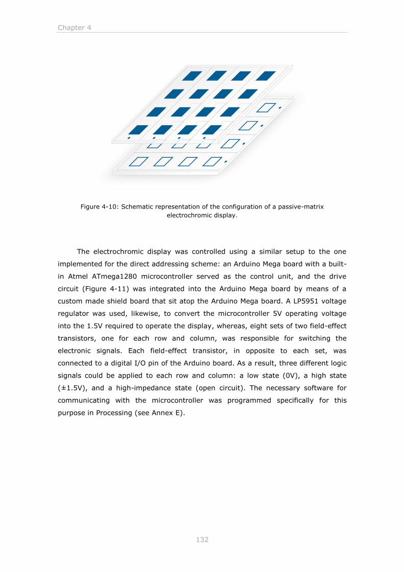
Chapter 4
132
Figure 4-10: Schematic representation of the configuration of a passive-matrix
electrochromic display.
The electrochromic display was controlled using a similar setup to the one
implemented for the direct addressing scheme: an Arduino Mega board with a built-
in Atmel ATmega1280 microcontroller served as the control unit, and the drive
circuit (Figure 4-11) was integrated into the Arduino Mega board by means of a
custom made shield board that sit atop the Arduino Mega board. A LP5951 voltage
regulator was used, likewise, to convert the microcontroller 5V operating voltage
into the 1.5V required to operate the display, whereas, eight sets of two field-effect
transistors, one for each row and column, was responsible for switching the
electronic signals. Each field-effect transistor, in opposite to each set, was
connected to a digital I/O pin of the Arduino board. As a result, three different logic
signals could be applied to each row and column: a low state (0V), a high state
(±1.5V), and a high-impedance state (open circuit). The necessary software for
communicating with the microcontroller was programmed specifically for this
purpose in Processing (see Annex E).
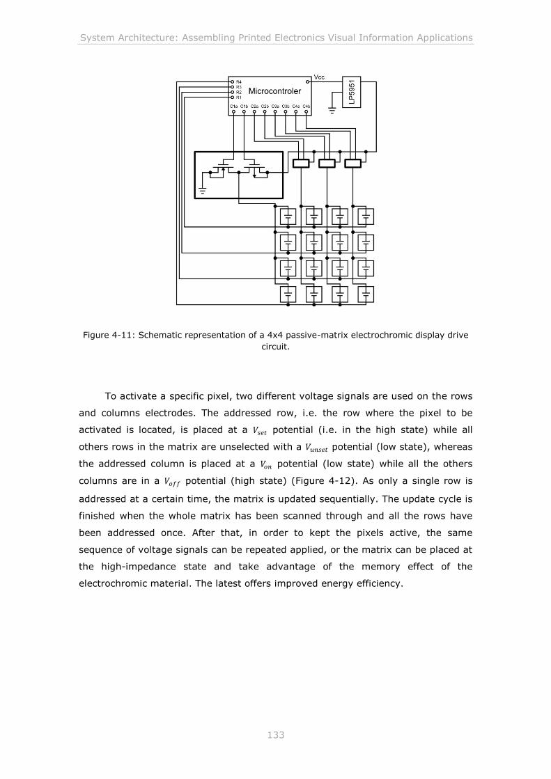
System Architecture: Assembling Printed Electronics Visual Information Applications
133
Figure 4-11: Schematic representation of a 4x4 passive-matrix electrochromic display drive
circuit.
To activate a specific pixel, two different voltage signals are used on the rows
and columns electrodes. The addressed row, i.e. the row where the pixel to be
activated is located, is placed at a 𝑉𝑠𝑒𝑡 potential (i.e. in the high state) while all
others rows in the matrix are unselected with a 𝑉𝑢𝑛𝑠𝑒𝑡 potential (low state), whereas
the addressed column is placed at a 𝑉𝑜𝑛 potential (low state) while all the others
columns are in a 𝑉𝑜𝑓𝑓 potential (high state) (Figure 4-12). As only a single row is
addressed at a certain time, the matrix is updated sequentially. The update cycle is
finished when the whole matrix has been scanned through and all the rows have
been addressed once. After that, in order to kept the pixels active, the same
sequence of voltage signals can be repeated applied, or the matrix can be placed at
the high-impedance state and take advantage of the memory effect of the
electrochromic material. The latest offers improved energy efficiency.
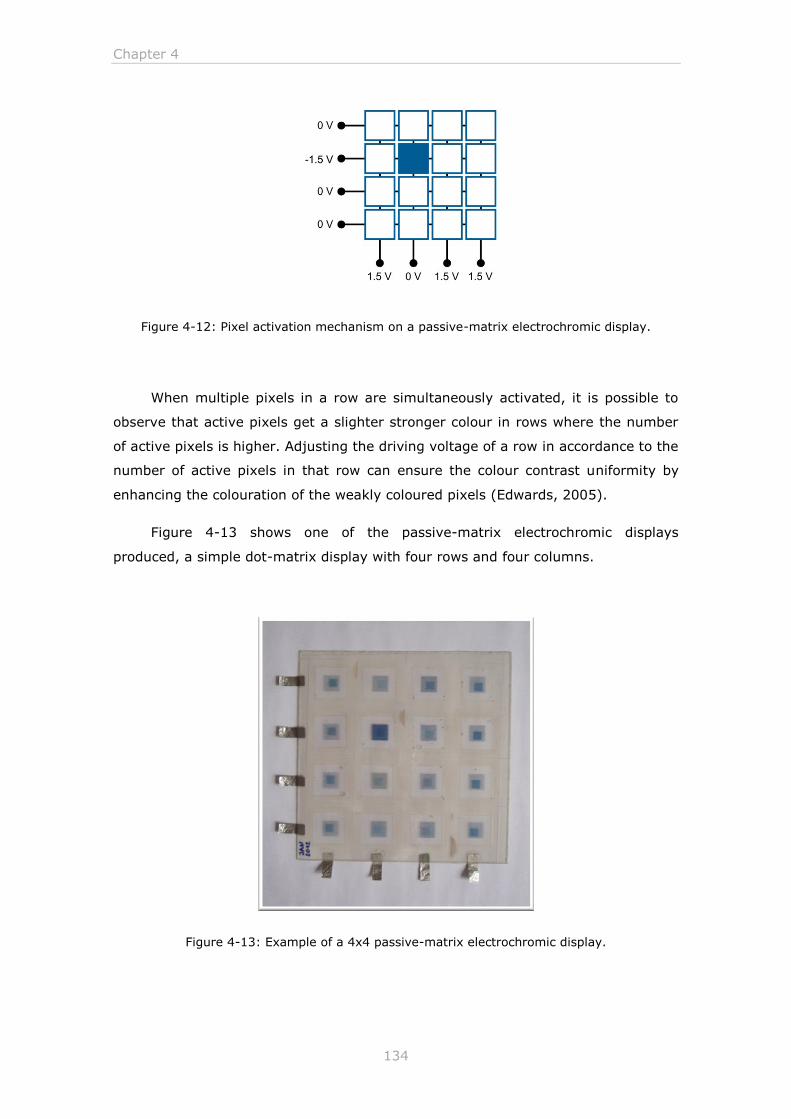
Chapter 4
134
Figure 4-12: Pixel activation mechanism on a passive-matrix electrochromic display.
When multiple pixels in a row are simultaneously activated, it is possible to
observe that active pixels get a slighter stronger colour in rows where the number
of active pixels is higher. Adjusting the driving voltage of a row in accordance to the
number of active pixels in that row can ensure the colour contrast uniformity by
enhancing the colouration of the weakly coloured pixels (Edwards, 2005).
Figure 4-13 shows one of the passive-matrix electrochromic displays
produced, a simple dot-matrix display with four rows and four columns.
Figure 4-13: Example of a 4x4 passive-matrix electrochromic display.
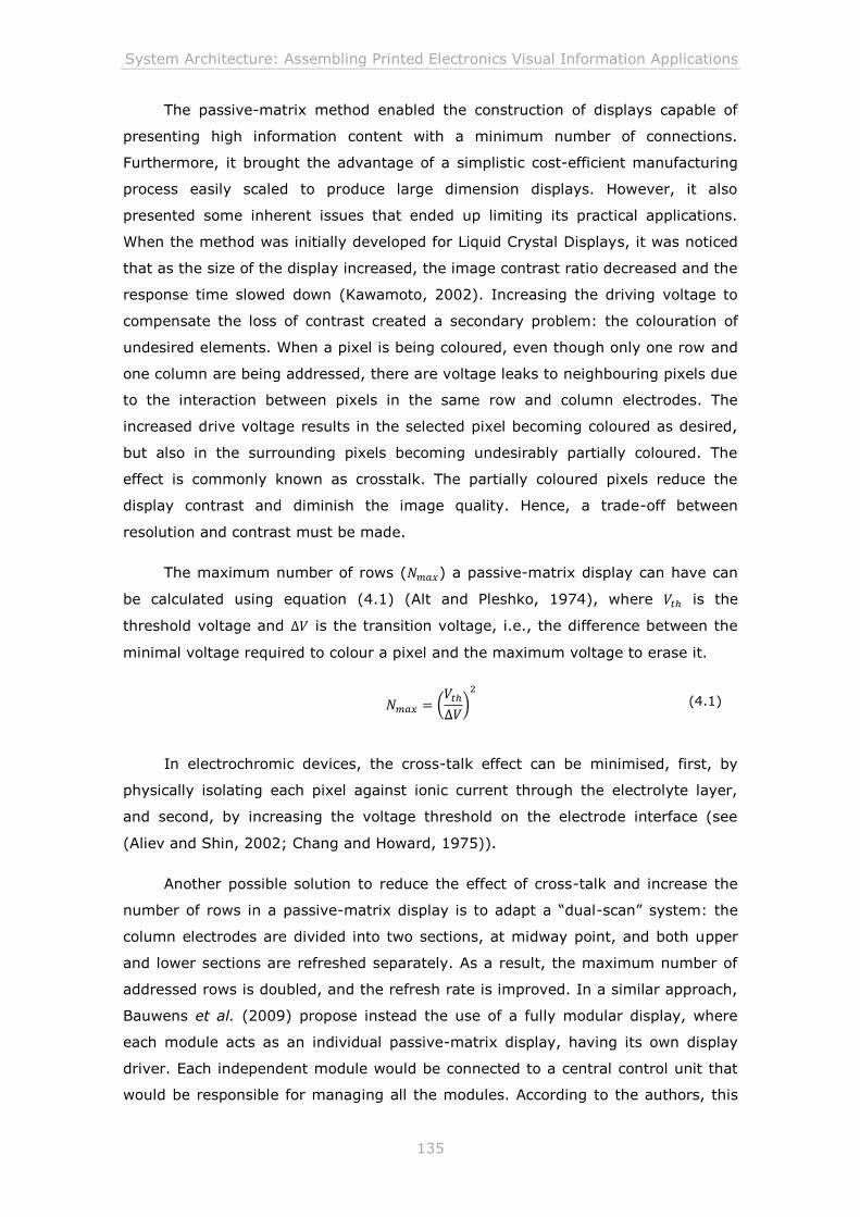
System Architecture: Assembling Printed Electronics Visual Information Applications
135
The passive-matrix method enabled the construction of displays capable of
presenting high information content with a minimum number of connections.
Furthermore, it brought the advantage of a simplistic cost-efficient manufacturing
process easily scaled to produce large dimension displays. However, it also
presented some inherent issues that ended up limiting its practical applications.
When the method was initially developed for Liquid Crystal Displays, it was noticed
that as the size of the display increased, the image contrast ratio decreased and the
response time slowed down (Kawamoto, 2002). Increasing the driving voltage to
compensate the loss of contrast created a secondary problem: the colouration of
undesired elements. When a pixel is being coloured, even though only one row and
one column are being addressed, there are voltage leaks to neighbouring pixels due
to the interaction between pixels in the same row and column electrodes. The
increased drive voltage results in the selected pixel becoming coloured as desired,
but also in the surrounding pixels becoming undesirably partially coloured. The
effect is commonly known as crosstalk. The partially coloured pixels reduce the
display contrast and diminish the image quality. Hence, a trade-off between
resolution and contrast must be made.
The maximum number of rows (𝑁𝑚𝑎𝑥) a passive-matrix display can have can
be calculated using equation (4.1) (Alt and Pleshko, 1974), where 𝑉𝑡ℎ is the
threshold voltage and ∆𝑉 is the transition voltage, i.e., the difference between the
minimal voltage required to colour a pixel and the maximum voltage to erase it.
𝑁𝑚𝑎𝑥 = (
𝑉𝑡ℎ
∆𝑉)
2
(4.1)
In electrochromic devices, the cross-talk effect can be minimised, first, by
physically isolating each pixel against ionic current through the electrolyte layer,
and second, by increasing the voltage threshold on the electrode interface (see
(Aliev and Shin, 2002; Chang and Howard, 1975)).
Another possible solution to reduce the effect of cross-talk and increase the
number of rows in a passive-matrix display is to adapt a “dual-scan” system: the
column electrodes are divided into two sections, at midway point, and both upper
and lower sections are refreshed separately. As a result, the maximum number of
addressed rows is doubled, and the refresh rate is improved. In a similar approach,
Bauwens et al. (2009) propose instead the use of a fully modular display, where
each module acts as an individual passive-matrix display, having its own display
driver. Each independent module would be connected to a central control unit that
would be responsible for managing all the modules. According to the authors, this
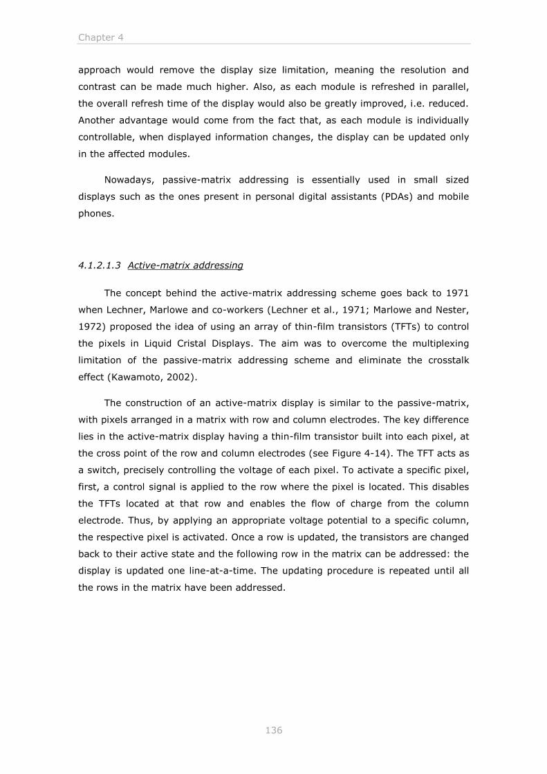
Chapter 4
136
approach would remove the display size limitation, meaning the resolution and
contrast can be made much higher. Also, as each module is refreshed in parallel,
the overall refresh time of the display would also be greatly improved, i.e. reduced.
Another advantage would come from the fact that, as each module is individually
controllable, when displayed information changes, the display can be updated only
in the affected modules.
Nowadays, passive-matrix addressing is essentially used in small sized
displays such as the ones present in personal digital assistants (PDAs) and mobile
phones.
4.1.2.1.3 Active-matrix addressing
The concept behind the active-matrix addressing scheme goes back to 1971
when Lechner, Marlowe and co-workers (Lechner et al., 1971; Marlowe and Nester,
1972) proposed the idea of using an array of thin-film transistors (TFTs) to control
the pixels in Liquid Cristal Displays. The aim was to overcome the multiplexing
limitation of the passive-matrix addressing scheme and eliminate the crosstalk
effect (Kawamoto, 2002).
The construction of an active-matrix display is similar to the passive-matrix,
with pixels arranged in a matrix with row and column electrodes. The key difference
lies in the active-matrix display having a thin-film transistor built into each pixel, at
the cross point of the row and column electrodes (see Figure 4-14). The TFT acts as
a switch, precisely controlling the voltage of each pixel. To activate a specific pixel,
first, a control signal is applied to the row where the pixel is located. This disables
the TFTs located at that row and enables the flow of charge from the column
electrode. Thus, by applying an appropriate voltage potential to a specific column,
the respective pixel is activated. Once a row is updated, the transistors are changed
back to their active state and the following row in the matrix can be addressed: the
display is updated one line-at-a-time. The updating procedure is repeated until all
the rows in the matrix have been addressed.
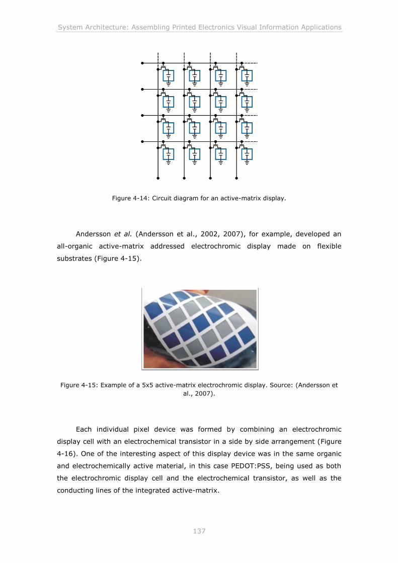
System Architecture: Assembling Printed Electronics Visual Information Applications
137
Figure 4-14: Circuit diagram for an active-matrix display.
Andersson et al. (Andersson et al., 2002, 2007), for example, developed an
all-organic active-matrix addressed electrochromic display made on flexible
substrates (Figure 4-15).
Figure 4-15: Example of a 5x5 active-matrix electrochromic display. Source: (Andersson et
al., 2007).
Each individual pixel device was formed by combining an electrochromic
display cell with an electrochemical transistor in a side by side arrangement (Figure
4-16). One of the interesting aspect of this display device was in the same organic
and electrochemically active material, in this case PEDOT:PSS, being used as both
the electrochromic display cell and the electrochemical transistor, as well as the
conducting lines of the integrated active-matrix.
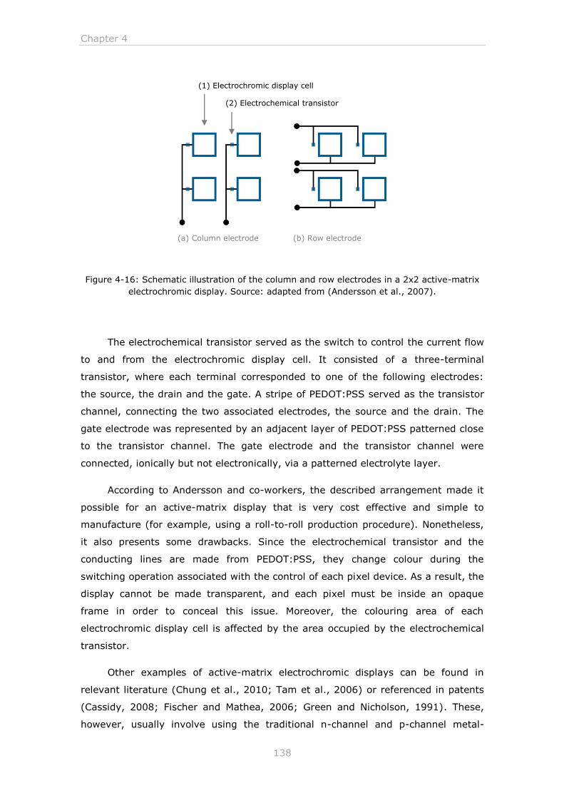
Chapter 4
138
Figure 4-16: Schematic illustration of the column and row electrodes in a 2x2 active-matrix
electrochromic display. Source: adapted from (Andersson et al., 2007).
The electrochemical transistor served as the switch to control the current flow
to and from the electrochromic display cell. It consisted of a three-terminal
transistor, where each terminal corresponded to one of the following electrodes:
the source, the drain and the gate. A stripe of PEDOT:PSS served as the transistor
channel, connecting the two associated electrodes, the source and the drain. The
gate electrode was represented by an adjacent layer of PEDOT:PSS patterned close
to the transistor channel. The gate electrode and the transistor channel were
connected, ionically but not electronically, via a patterned electrolyte layer.
According to Andersson and co-workers, the described arrangement made it
possible for an active-matrix display that is very cost effective and simple to
manufacture (for example, using a roll-to-roll production procedure). Nonetheless,
it also presents some drawbacks. Since the electrochemical transistor and the
conducting lines are made from PEDOT:PSS, they change colour during the
switching operation associated with the control of each pixel device. As a result, the
display cannot be made transparent, and each pixel must be inside an opaque
frame in order to conceal this issue. Moreover, the colouring area of each
electrochromic display cell is affected by the area occupied by the electrochemical
transistor.
Other examples of active-matrix electrochromic displays can be found in
relevant literature (Chung et al., 2010; Tam et al., 2006) or referenced in patents
(Cassidy, 2008; Fischer and Mathea, 2006; Green and Nicholson, 1991). These,
however, usually involve using the traditional n-channel and p-channel metal-
(a) Column electrode (b) Row electrode
(2) Electrochemical transistor
(1) Electrochromic display cell
-
System Architecture: Assembling Printed Electronics Visual Information Applications
139
oxide-semiconductor TFTs and typically placing them at the display backplane. The
biggest advantage in this approach, i.e. in placing the TFTs in the display
backplane, is in the maximisation of the viewable pixel area.
In sum, the active-matrix addressing scheme solved the problems associated
with passive-matrix displays, such as the scanning limitations and the crosstalk
effect, as well as the contrast ratio and grey scale limitations. However, the cost
and complexity of manufacturing an active-matrix display is also higher than a
passive-matrix. Hence, its implementation should be pondered according to the
type of application.
4.2 Types of content
The possible applications for electrochromic displays are numerous: from
being integrated in traditional print magazines and posters to products packages
and point of purchase (POP) locations or in signage systems. However, its
successful deployment is greatly dependent on its visual content. It must be
exciting and relevant, captivating and engaging users and consumers.
This section addresses the topic of content formats in electrochromic displays,
focusing on the creation of interactive and dynamic visual content. Based on the
different addressing methods described in section 4.1.2.1 and on the potential to
create dynamic content and animations, six different formats of visual content were
distinguished. Table 4-2 summarises the different categories of visual content and
the necessary architectures for displaying it. The designation of each category
intends to capture the uniqueness of that specific category in relation to the others.
In the following sub-sections, the six different types of content as well as the
necessary architecture to reproduce them are described in detail. It provides a first
glimpse of what could emerge as an inexpensive and creative platform for bridging
the worlds of bits and atoms. The examples developed for each type of
architecture/content illustrate how these can be implemented as simple, task-
specific applications (though they are still rough prototypes) following an end-user
fabrication process. All the materials and electronic components used to make the
devices are easily purchasable online by anyone or in any electronics specialty
store.
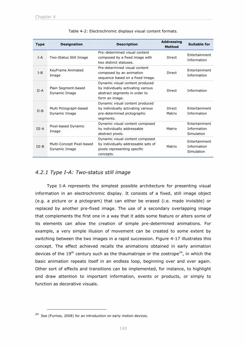
Chapter 4
140
Table 4-2: Electrochromic displays visual content formats.
Type Designation Description Addressing
Method Suitable for
I-A Two-Status Still Image
Pre–determined visual content
composed by a fixed image with
two distinct statuses.
Direct Entertainment
Information
I-B KeyFrame Animated
Image
Pre-determined visual content
composed by an animation
sequence based on a fixed image.
Direct Entertainment
Information
II-A Plain Segment-based
Dynamic Image
Dynamic visual content produced
by individually activating various
abstract segments in order to
form an image.
Direct Information
II-B Multi Pictograph-based
Dynamic Image
Dynamic visual content produced
by individually activating various
pre-determined pictographic
segments.
Direct
Matrix
Entertainment
Information
III-A Pixel-based Dynamic
Image
Dynamic visual content composed
by individually addressable
abstract pixels.
Matrix
Entertainment
Information
Simulation
III-B Multi-Concept Pixel-based
Dynamic Image
Dynamic visual content composed
by individually addressable sets of
pixels representing specific
concepts.
Matrix
Entertainment
Information
Simulation
4.2.1 Type I-A: Two-status still image
Type I-A represents the simplest possible architecture for presenting visual
information in an electrochromic display. It consists of a fixed, still image object
(e.g. a picture or a pictogram) that can either be erased (i.e. made invisible) or
replaced by another pre-fixed image. The use of a secondary overlapping image
that complements the first one in a way that it adds some feature or alters some of
its elements can allow the creation of simple pre-determined animations. For
example, a very simple illusion of movement can be created to some extent by
switching between the two images in a rapid succession. Figure 4-17 illustrates this
concept. The effect achieved recalls the animations obtained in early animation
devices of the 19th century such as the thaumatrope or the zoetrope24, in which the
basic animation repeats itself in an endless loop, beginning over and over again.
Other sort of effects and transitions can be implemented, for instance, to highlight
and draw attention to important information, events or products, or simply to
function as decorative visuals.
24
See (Furniss, 2008) for an introduction on early motion devices.
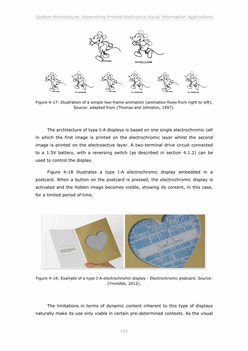
System Architecture: Assembling Printed Electronics Visual Information Applications
141
Figure 4-17: Illustration of a simple two-frame animation (animation flows from right to left).
Source: adapted from (Thomas and Johnston, 1997).
The architecture of type I-A displays is based on one single electrochromic cell
in which the first image is printed on the electrochromic layer whilst the second
image is printed on the electroactive layer. A two-terminal drive circuit connected
to a 1.5V battery, with a reversing switch (as described in section 4.1.2) can be
used to control the display.
Figure 4-18 illustrates a type I-A electrochromic display embedded in a
postcard. When a button on the postcard is pressed, the electrochromic display is
activated and the hidden image becomes visible, showing its content, in this case,
for a limited period of time.
Figure 4-18: Example of a type I-A electrochromic display - Electrochromic postcard. Source:
(Ynvisible, 2012).
The limitations in terms of dynamic content inherent to this type of displays
naturally make its use only viable in certain pre-determined contexts. As the visual
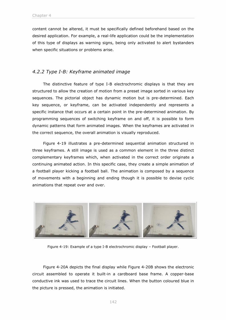
Chapter 4
142
content cannot be altered, it must be specifically defined beforehand based on the
desired application. For example, a real-life application could be the implementation
of this type of displays as warning signs, being only activated to alert bystanders
when specific situations or problems arise.
4.2.2 Type I-B: Keyframe animated image
The distinctive feature of type I-B electrochromic displays is that they are
structured to allow the creation of motion from a preset image sorted in various key
sequences. The pictorial object has dynamic motion but is pre-determined. Each
key sequence, or keyframe, can be activated independently and represents a
specific instance that occurs at a certain point in the pre-determined animation. By
programming sequences of switching keyframe on and off, it is possible to form
dynamic patterns that form animated images. When the keyframes are activated in
the correct sequence, the overall animation is visually reproduced.
Figure 4-19 illustrates a pre-determined sequential animation structured in
three keyframes. A still image is used as a common element in the three distinct
complementary keyframes which, when activated in the correct order originate a
continuing animated action. In this specific case, they create a simple animation of
a football player kicking a football ball. The animation is composed by a sequence
of movements with a beginning and ending though it is possible to devise cyclic
animations that repeat over and over.
Figure 4-19: Example of a type I-B electrochromic display – Football player.
Figure 4-20A depicts the final display while Figure 4-20B shows the electronic
circuit assembled to operate it built-in a cardboard base frame. A copper-base
conductive ink was used to trace the circuit lines. When the button coloured blue in
the picture is pressed, the animation is initiated.
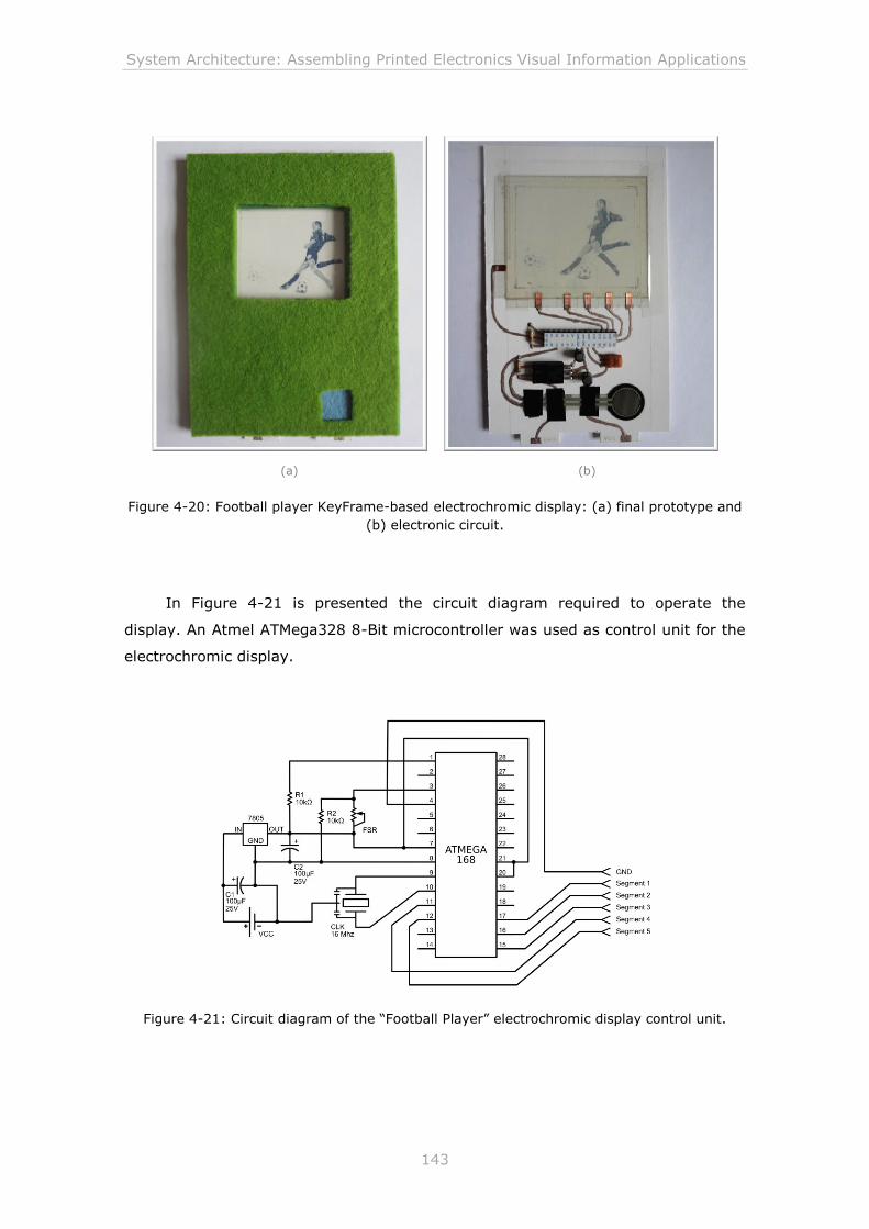
System Architecture: Assembling Printed Electronics Visual Information Applications
143
Figure 4-20: Football player KeyFrame-based electrochromic display: (a) final prototype and
(b) electronic circuit.
In Figure 4-21 is presented the circuit diagram required to operate the
display. An Atmel ATMega328 8-Bit microcontroller was used as control unit for the
electrochromic display.
Figure 4-21: Circuit diagram of the “Football Player” electrochromic display control unit.
(a) (b)
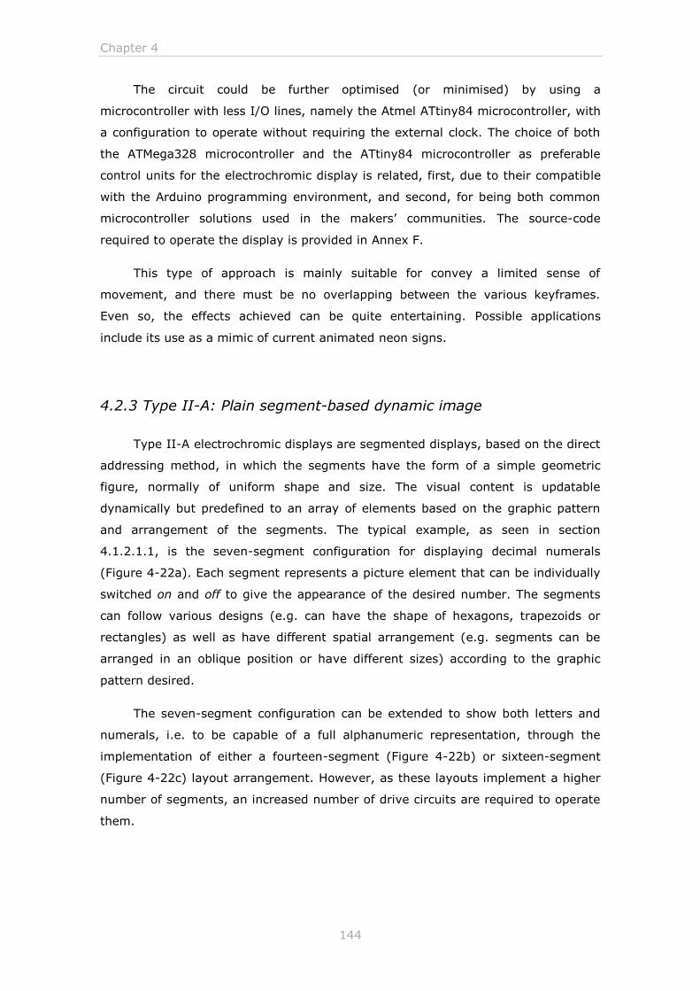
Chapter 4
144
The circuit could be further optimised (or minimised) by using a
microcontroller with less I/O lines, namely the Atmel ATtiny84 microcontroller, with
a configuration to operate without requiring the external clock. The choice of both
the ATMega328 microcontroller and the ATtiny84 microcontroller as preferable
control units for the electrochromic display is related, first, due to their compatible
with the Arduino programming environment, and second, for being both common
microcontroller solutions used in the makers’ communities. The source-code
required to operate the display is provided in Annex F.
This type of approach is mainly suitable for convey a limited sense of
movement, and there must be no overlapping between the various keyframes.
Even so, the effects achieved can be quite entertaining. Possible applications
include its use as a mimic of current animated neon signs.
4.2.3 Type II-A: Plain segment-based dynamic image
Type II-A electrochromic displays are segmented displays, based on the direct
addressing method, in which the segments have the form of a simple geometric
figure, normally of uniform shape and size. The visual content is updatable
dynamically but predefined to an array of elements based on the graphic pattern
and arrangement of the segments. The typical example, as seen in section
4.1.2.1.1, is the seven-segment configuration for displaying decimal numerals
(Figure 4-22a). Each segment represents a picture element that can be individually
switched on and off to give the appearance of the desired number. The segments
can follow various designs (e.g. can have the shape of hexagons, trapezoids or
rectangles) as well as have different spatial arrangement (e.g. segments can be
arranged in an oblique position or have different sizes) according to the graphic
pattern desired.
The seven-segment configuration can be extended to show both letters and
numerals, i.e. to be capable of a full alphanumeric representation, through the
implementation of either a fourteen-segment (Figure 4-22b) or sixteen-segment
(Figure 4-22c) layout arrangement. However, as these layouts implement a higher
number of segments, an increased number of drive circuits are required to operate
them.
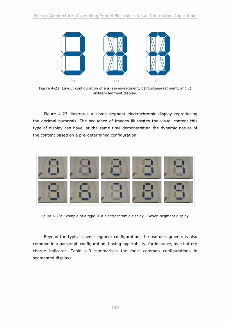
System Architecture: Assembling Printed Electronics Visual Information Applications
145
Figure 4-22: Layout configuration of a a) seven-segment, b) fourteen-segment, and c)
sixteen-segment display.
Figure 4-23 illustrates a seven-segment electrochromic display reproducing
the decimal numerals. The sequence of images illustrates the visual content this
type of display can have, at the same time demonstrating the dynamic nature of
the content based on a pre-determined configuration.
Figure 4-23: Example of a type II-A electrochromic display - Seven-segment display.
Beyond the typical seven-segment configuration, the use of segments is also
common in a bar graph configuration, having applicability, for instance, as a battery
charge indicator. Table 4-3 summarises the most common configurations in
segmented displays.
(a) (b) (c)
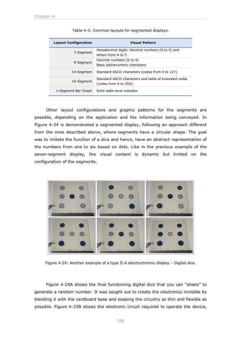
Chapter 4
146
Table 4-3: Common layouts for segmented displays.
Layout Configuration Visual Pattern
7-Segment Hexadecimal digits: Decimal numbers (0 to 9) and
letters from A to F.
9-Segment Decimal numbers (0 to 9)
Basic alphanumeric characters
14-Segment Standard ASCII characters (codes from 0 to 127).
16-Segment Standard ASCII characters and table of extended codes
(codes from 0 to 255).
n-Segment Bar Graph Solid state level indicator
Other layout configurations and graphic patterns for the segments are
possible, depending on the application and the information being conveyed. In
Figure 4-24 is demonstrated a segmented display, following an approach different
from the ones described above, where segments have a circular shape. The goal
was to imitate the function of a dice and hence, have an abstract representation of
the numbers from one to six based on dots. Like in the previous example of the
seven-segment display, the visual content is dynamic but limited on the
configuration of the segments.
Figure 4-24: Another example of a type II-A electrochromic display – Digital dice.
Figure 4-25A shows the final functioning digital dice that you can “shake” to
generate a random number. It was sought out to create the electronics invisible by
blending it with the cardboard base and keeping the circuitry as thin and flexible as
possible. Figure 4-25B shows the electronic circuit required to operate the device,
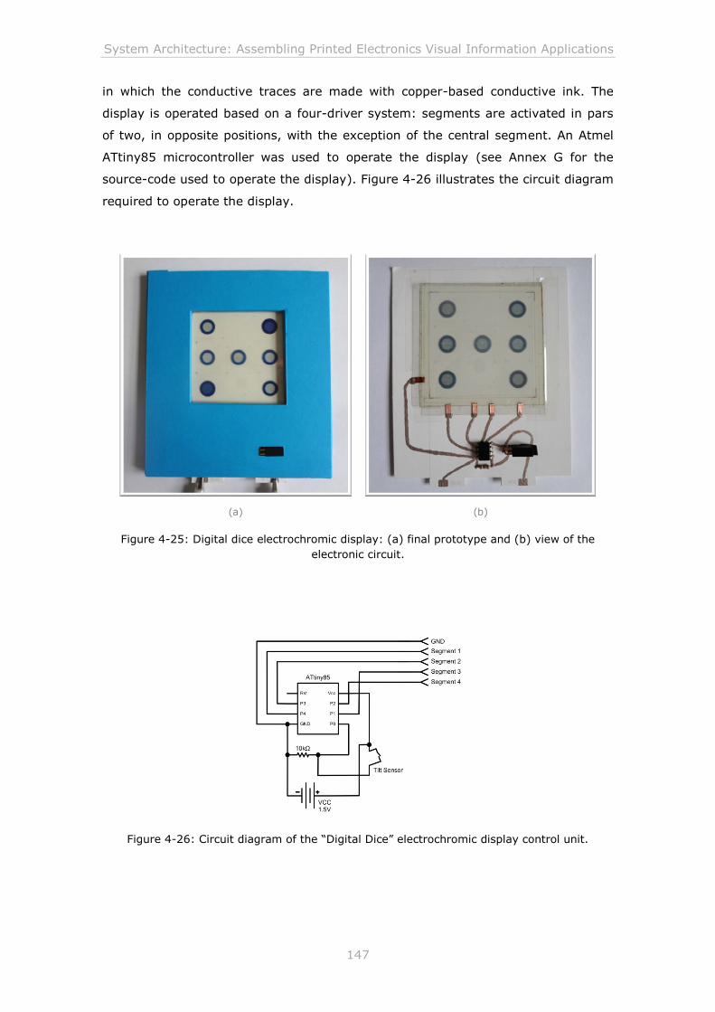
System Architecture: Assembling Printed Electronics Visual Information Applications
147
in which the conductive traces are made with copper-based conductive ink. The
display is operated based on a four-driver system: segments are activated in pars
of two, in opposite positions, with the exception of the central segment. An Atmel
ATtiny85 microcontroller was used to operate the display (see Annex G for the
source-code used to operate the display). Figure 4-26 illustrates the circuit diagram
required to operate the display.
Figure 4-25: Digital dice electrochromic display: (a) final prototype and (b) view of the
electronic circuit.
Figure 4-26: Circuit diagram of the “Digital Dice” electrochromic display control unit.
(a) (b)
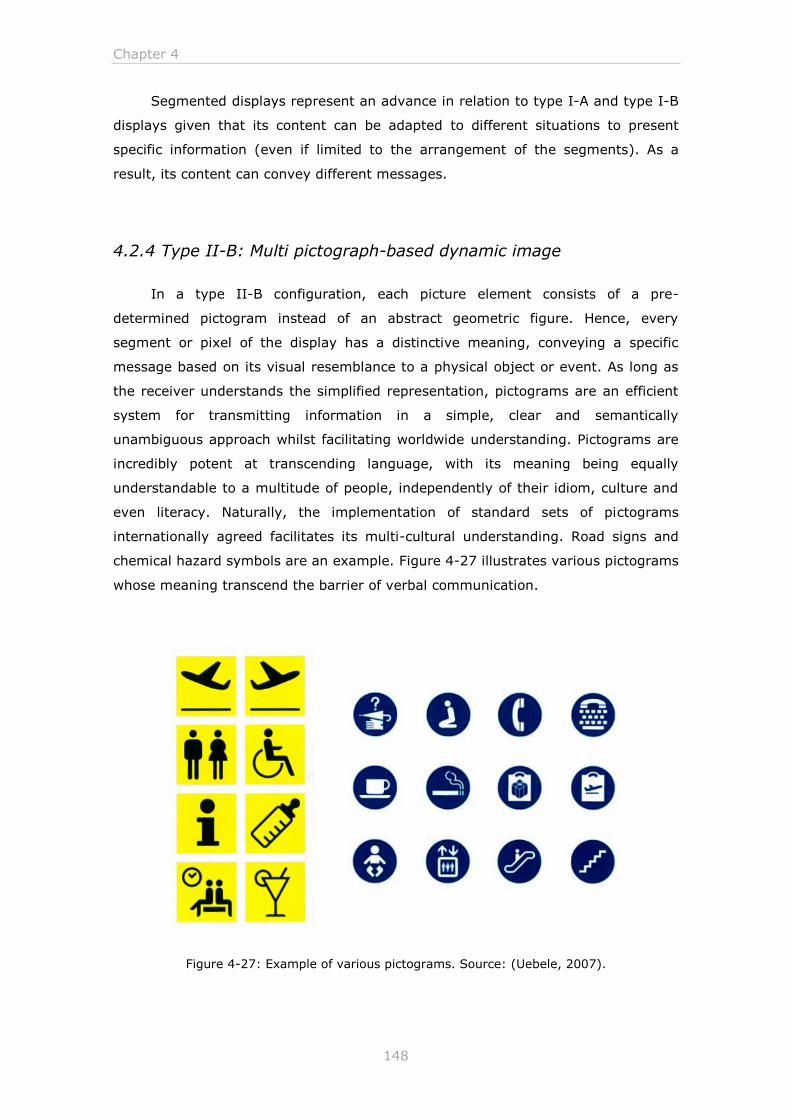
Chapter 4
148
Segmented displays represent an advance in relation to type I-A and type I-B
displays given that its content can be adapted to different situations to present
specific information (even if limited to the arrangement of the segments). As a
result, its content can convey different messages.
4.2.4 Type II-B: Multi pictograph-based dynamic image
In a type II-B configuration, each picture element consists of a pre-
determined pictogram instead of an abstract geometric figure. Hence, every
segment or pixel of the display has a distinctive meaning, conveying a specific
message based on its visual resemblance to a physical object or event. As long as
the receiver understands the simplified representation, pictograms are an efficient
system for transmitting information in a simple, clear and semantically
unambiguous approach whilst facilitating worldwide understanding. Pictograms are
incredibly potent at transcending language, with its meaning being equally
understandable to a multitude of people, independently of their idiom, culture and
even literacy. Naturally, the implementation of standard sets of pictograms
internationally agreed facilitates its multi-cultural understanding. Road signs and
chemical hazard symbols are an example. Figure 4-27 illustrates various pictograms
whose meaning transcend the barrier of verbal communication.
Figure 4-27: Example of various pictograms. Source: (Uebele, 2007).
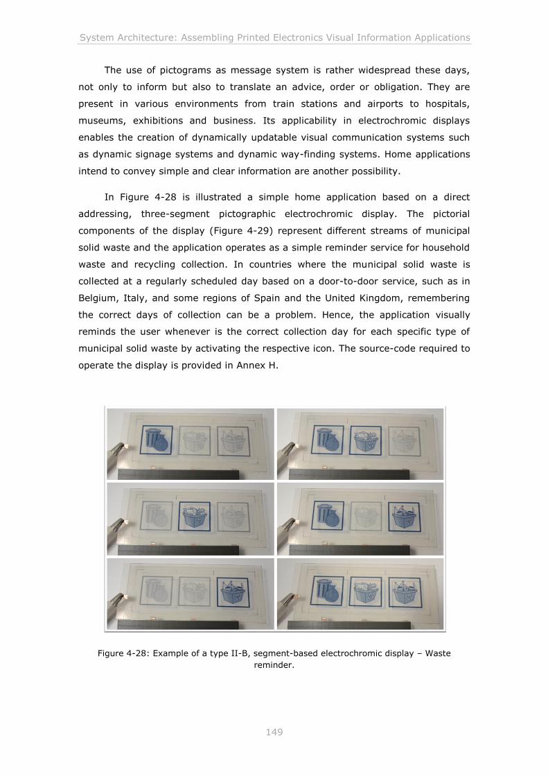
System Architecture: Assembling Printed Electronics Visual Information Applications
149
The use of pictograms as message system is rather widespread these days,
not only to inform but also to translate an advice, order or obligation. They are
present in various environments from train stations and airports to hospitals,
museums, exhibitions and business. Its applicability in electrochromic displays
enables the creation of dynamically updatable visual communication systems such
as dynamic signage systems and dynamic way-finding systems. Home applications
intend to convey simple and clear information are another possibility.
In Figure 4-28 is illustrated a simple home application based on a direct
addressing, three-segment pictographic electrochromic display. The pictorial
components of the display (Figure 4-29) represent different streams of municipal
solid waste and the application operates as a simple reminder service for household
waste and recycling collection. In countries where the municipal solid waste is
collected at a regularly scheduled day based on a door-to-door service, such as in
Belgium, Italy, and some regions of Spain and the United Kingdom, remembering
the correct days of collection can be a problem. Hence, the application visually
reminds the user whenever is the correct collection day for each specific type of
municipal solid waste by activating the respective icon. The source-code required to
operate the display is provided in Annex H.
Figure 4-28: Example of a type II-B, segment-based electrochromic display – Waste
reminder.
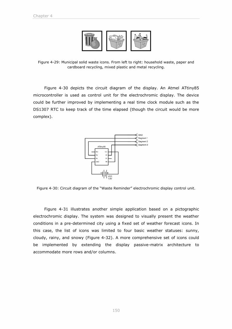
Chapter 4
150
Figure 4-29: Municipal solid waste icons. From left to right: household waste, paper and
cardboard recycling, mixed plastic and metal recycling.
Figure 4-30 depicts the circuit diagram of the display. An Atmel ATtiny85
microcontroller is used as control unit for the electrochromic display. The device
could be further improved by implementing a real time clock module such as the
DS1307 RTC to keep track of the time elapsed (though the circuit would be more
complex).
Figure 4-30: Circuit diagram of the “Waste Reminder” electrochromic display control unit.
Figure 4-31 illustrates another simple application based on a pictographic
electrochromic display. The system was designed to visually present the weather
conditions in a pre-determined city using a fixed set of weather forecast icons. In
this case, the list of icons was limited to four basic weather statuses: sunny,
cloudy, rainy, and snowy (Figure 4-32). A more comprehensive set of icons could
be implemented by extending the display passive-matrix architecture to
accommodate more rows and/or columns.
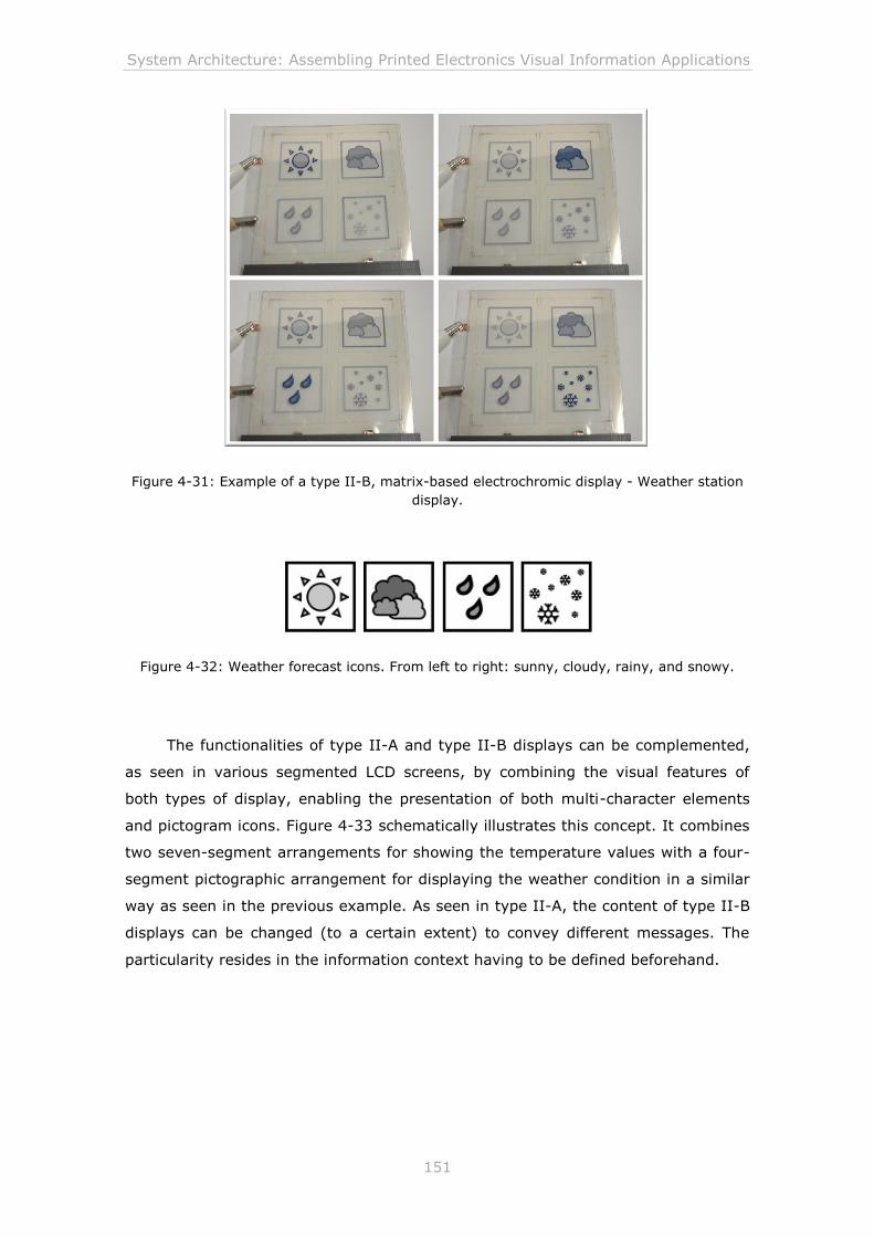
System Architecture: Assembling Printed Electronics Visual Information Applications
151
Figure 4-31: Example of a type II-B, matrix-based electrochromic display - Weather station
display.
Figure 4-32: Weather forecast icons. From left to right: sunny, cloudy, rainy, and snowy.
The functionalities of type II-A and type II-B displays can be complemented,
as seen in various segmented LCD screens, by combining the visual features of
both types of display, enabling the presentation of both multi-character elements
and pictogram icons. Figure 4-33 schematically illustrates this concept. It combines
two seven-segment arrangements for showing the temperature values with a four-
segment pictographic arrangement for displaying the weather condition in a similar
way as seen in the previous example. As seen in type II-A, the content of type II-B
displays can be changed (to a certain extent) to convey different messages. The
particularity resides in the information context having to be defined beforehand.
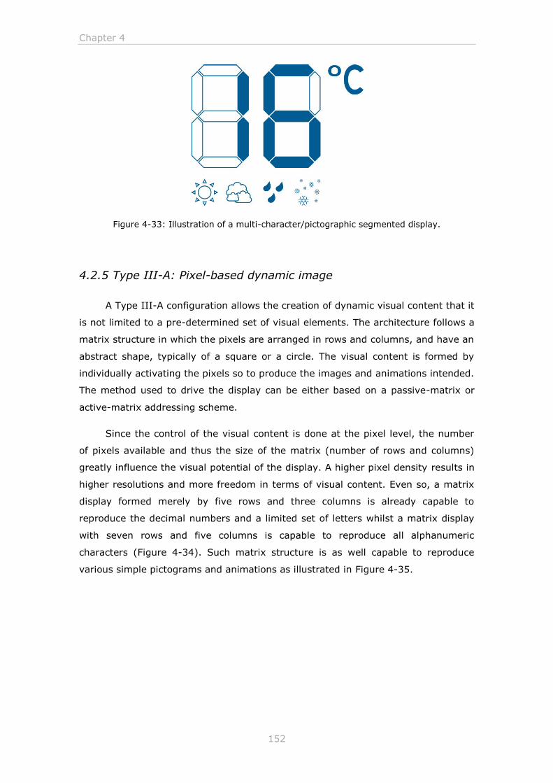
Chapter 4
152
Figure 4-33: Illustration of a multi-character/pictographic segmented display.
4.2.5 Type III-A: Pixel-based dynamic image
A Type III-A configuration allows the creation of dynamic visual content that it
is not limited to a pre-determined set of visual elements. The architecture follows a
matrix structure in which the pixels are arranged in rows and columns, and have an
abstract shape, typically of a square or a circle. The visual content is formed by
individually activating the pixels so to produce the images and animations intended.
The method used to drive the display can be either based on a passive-matrix or
active-matrix addressing scheme.
Since the control of the visual content is done at the pixel level, the number
of pixels available and thus the size of the matrix (number of rows and columns)
greatly influence the visual potential of the display. A higher pixel density results in
higher resolutions and more freedom in terms of visual content. Even so, a matrix
display formed merely by five rows and three columns is already capable to
reproduce the decimal numbers and a limited set of letters whilst a matrix display
with seven rows and five columns is capable to reproduce all alphanumeric
characters (Figure 4-34). Such matrix structure is as well capable to reproduce
various simple pictograms and animations as illustrated in Figure 4-35.
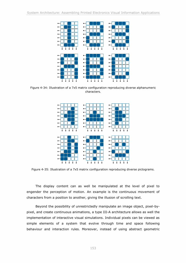
System Architecture: Assembling Printed Electronics Visual Information Applications
153
Figure 4-34: Illustration of a 7x5 matrix configuration reproducing diverse alphanumeric
characters.
Figure 4-35: Illustration of a 7x5 matrix configuration reproducing diverse pictograms.
The display content can as well be manipulated at the level of pixel to
engender the perception of motion. An example is the continuous movement of
characters from a position to another, giving the illusion of scrolling text.
Beyond the possibility of unrestrictedly manipulate an image object, pixel-by-
pixel, and create continuous animations, a type III-A architecture allows as well the
implementation of interactive visual simulations. Individual pixels can be viewed as
simple elements of a system that evolve through time and space following
behaviour and interaction rules. Moreover, instead of using abstract geometric
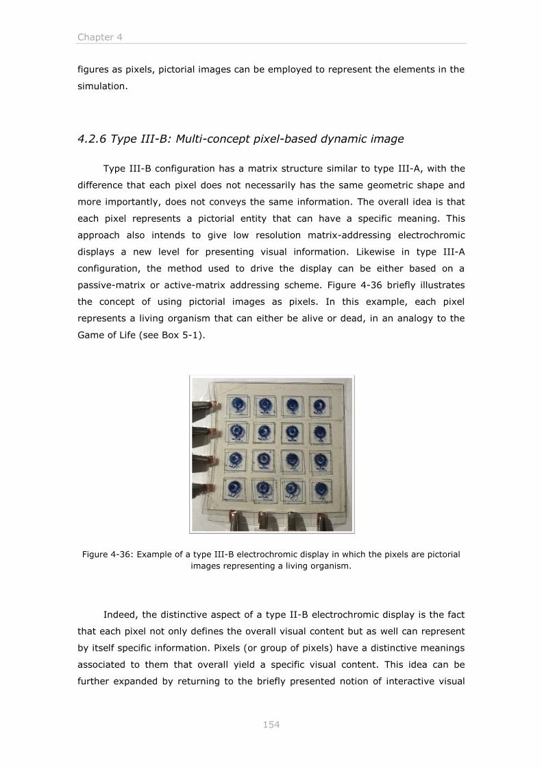
Chapter 4
154
figures as pixels, pictorial images can be employed to represent the elements in the
simulation.
4.2.6 Type III-B: Multi-concept pixel-based dynamic image
Type III-B configuration has a matrix structure similar to type III-A, with the
difference that each pixel does not necessarily has the same geometric shape and
more importantly, does not conveys the same information. The overall idea is that
each pixel represents a pictorial entity that can have a specific meaning. This
approach also intends to give low resolution matrix-addressing electrochromic
displays a new level for presenting visual information. Likewise in type III-A
configuration, the method used to drive the display can be either based on a
passive-matrix or active-matrix addressing scheme. Figure 4-36 briefly illustrates
the concept of using pictorial images as pixels. In this example, each pixel
represents a living organism that can either be alive or dead, in an analogy to the
Game of Life (see Box 5-1).
Figure 4-36: Example of a type III-B electrochromic display in which the pixels are pictorial
images representing a living organism.
Indeed, the distinctive aspect of a type II-B electrochromic display is the fact
that each pixel not only defines the overall visual content but as well can represent
by itself specific information. Pixels (or group of pixels) have a distinctive meanings
associated to them that overall yield a specific visual content. This idea can be
further expanded by returning to the briefly presented notion of interactive visual
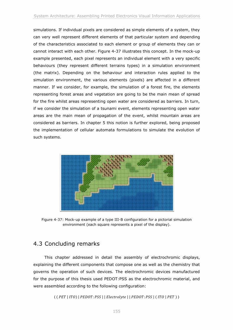
System Architecture: Assembling Printed Electronics Visual Information Applications
155
simulations. If individual pixels are considered as simple elements of a system, they
can very well represent different elements of that particular system and depending
of the characteristics associated to each element or group of elements they can or
cannot interact with each other. Figure 4-37 illustrates this concept. In the mock-up
example presented, each pixel represents an individual element with a very specific
behaviours (they represent different terrains types) in a simulation environment
(the matrix). Depending on the behaviour and interaction rules applied to the
simulation environment, the various elements (pixels) are affected in a different
manner. If we consider, for example, the simulation of a forest fire, the elements
representing forest areas and vegetation are going to be the main mean of spread
for the fire whilst areas representing open water are considered as barriers. In turn,
if we consider the simulation of a tsunami event, elements representing open water
areas are the main mean of propagation of the event, whilst mountain areas are
considered as barriers. In chapter 5 this notion is further explored, being proposed
the implementation of cellular automata formulations to simulate the evolution of
such systems.
Figure 4-37: Mock-up example of a type III-B configuration for a pictorial simulation
environment (each square represents a pixel of the display).
4.3 Concluding remarks
This chapter addressed in detail the assembly of electrochromic displays,
explaining the different components that compose one as well as the chemistry that
governs the operation of such devices. The electrochromic devices manufactured
for the purpose of this thesis used PEDOT:PSS as the electrochromic material, and
were assembled according to the following configuration:
⟨ ( 𝑃𝐸𝑇 | 𝐼𝑇𝑂) | 𝑃𝐸𝐷𝑂𝑇: 𝑃𝑆𝑆 | | 𝐸𝑙𝑒𝑐𝑡𝑟𝑜𝑙𝑦𝑡𝑒 | | 𝑃𝐸𝐷𝑂𝑇: 𝑃𝑆𝑆 | ( 𝐼𝑇𝑂 | 𝑃𝐸𝑇 ) ⟩
Chapter 4
156
The choice of PEDOT:PSS as the electrochromic material was mainly because
of its proprieties, in particular, its high chemical stability in normal conditions; its
high transparency in thin, oxidised films; and its low electronic bandgap; as well as
due to the fact that it can be processed from a water emulsion and easily deposited
in various substrate, both rigid and flexible, by means of inkjet printing.
Design configurations regarding the control of individual picture elements in
electrochromic displays were also tackled. The three main addressing methods
explored were: (1) direct addressing, (2) passive-matrix addressing, and (3)
active-matrix addressing. Each method has its advantages and challenges. The
selection of one method over other influences the architecture and construction of
the display, as well as the functioning of the microcontroller responsible for
operating the display. The implementation of a particular addressing method in an
electrochromic display is closely related to its desired application, the information
content to be displayed and the production cost. The display area and the response
time can also have influence in the choice.
Direct addressing is essentially convenient for display applications where
there are only a reduced number of elements that have to be activated (e.g.
alphanumeric displays). Given that in direct addressing displays, each picture
element (commonly called segment) requires an individual connection, increasing
the number of segments to further increase the information content of the display
can significantly raise the number of connections to a point where managing all
becomes too complicated, ultimately becoming unpractical due to the high cost of
using so many drivers and the absence of space between elements for the higher
number of connections.
Passive-matrix addressing solved the limitations of direct addressing in
present high information content by moving to a scheme composed by pixels
arranged in a matrix with row and column electrodes. The novelty was in the
picture elements, i.e. the pixels, being addressed by their row and column instead
of being driven separately. Moreover, the simplicity of the scheme also made it very
cost-efficient. However, it also raised new issues that ended up limiting its practical
applicability. As the size of the passive-matrix increased, the image contrast ratio
decreased and the response time slowed down. Also, it was observed voltage leaks
between neighbouring pixels in the same row or column electrodes, resulting in the
colouration of undesirable elements (crosstalk effect).
Finally, the active-matrix addressing scheme appears as a solution to the
problems associated with passive-matrix displays, such as the scanning limitations
System Architecture: Assembling Printed Electronics Visual Information Applications
157
and crosstalk effect. The construction is similar to the passive-matrix, with pixels
arranged in a matrix with row and column electrodes. However, active-matrix
display have a thin-film transistor built into each pixel, at the cross point of the row
and column electrodes. The TFT acts as a switch, precisely controlling the voltage of
each pixel. The drawback of the active-matrix scheme when compared to the
passive-matrix is mainly related to its higher cost and manufacturing complexity.
The different types of display architecture/content detailed in this chapter
highlight how electrochromic displays can be used to present different levels of
visual information. It intends to provide a clear view of the various possibilities
offered and what can be expected to be achieved in terms of dynamic content. The
complexity of the architecture of the different arrangements increases from type I
to type III, likewise the potential for presenting dynamic information.
The dominant feature of type I displays is that content is pre-determined and
limited to a fixed number of difference instances. In type I-A, the maximum
number of instances is two whilst in type I-B the content is segmented to provide
multiple instances of the same image. In turn, the particularity of type II displays
lies in the content being updatable but limited to a fix pre-set of arrangements
based on layout of the composing segments. In type II-A displays, the individually
addressed segments are composed by abstract elements that can be combined to
form numbers, letter or symbols whilst in type II-B, the segments are composed by
individual pictograms, each one with a very specific meaning. Finally, in type III
displays, the matrix structure of the display allow the creation of dynamic content
through the differentiate control of the different picture elements. Type III-A
represents the typical all-purpose matrix arrangement display, where it is possible
to create multiple compositions and animations whilst the type III-B represents a
arrangement where a specific meaning is associated to each individual picture
elements that influences the overall visual content of the display. An envisaged
application, addressed in detail in the next chapter, is the use of such arrangement
as a means to display simulations based on pictorial elements performed by cellular
automata models in real time.
Electrochromic displays are still in their infancy stage in terms of real word
applications, and hence, experimentation in real world contexts is still necessary.
The various examples advanced here intend not only to demonstrate the different
types of architecture/content but as well provide insights for possible applications.
The particular technical universe explored showed to be appropriate for making
interactive devices. With the exception of Type III-B displays (which were only
idealised), all examples were developed using off-the-shelf components and
Chapter 4
158
hardware. A key point was to allow for user participation in the creation of the
devices themselves. Naturally, it would be interesting to see how the makers’
communities would embrace and use this technology in their projects, considering
the vast array of possibilities for customisation.
Computing with Simple Programs
159
5 Computing with Simple Programs
5.1 The world of cellular automata
In the late forties, the mathematician John von Neumann was trying to
formalise an abstract model of self-reproduction in biology. Following a suggestion
from his friend and fellow mathematician Stanislaw Ulam, of using a discrete
system for creating a reductionist model of a self-replication machine (Mitchell,
2009: 123; Wolfram, 2002: 876), von Neumann envisaged a checkerboard look-
like system, in which each square was a finite state automaton. In this particular
system, each cell could be in one of twenty-nine possible different states and would
follow pre-determined rules specifically set up to create a perfect reproduction of
any initial pattern placed on the cellular automaton lattice (see Neumann, 1966).
Von Neumann’s mathematical formulation of a self-replicating automaton was at
the time a major advance in the field of artificial life, demonstrating that a) self-
reproduction by machines was in theory possible and b) fairly simple rules could
form complex patterns. Moreover, he demonstrated that the devised cellular
automata could execute any computable operation. However, due to its complexity,
Von Neumann rules were never implemented on a computer.
In 2002, Stephen Wolfram published a likewise acclaimed (see Rucker, 2003)
and controversial (see Giles, 2002) book entitled “A New Kind of Science” (or NKS
for short) (Wolfram, 2002). In it, Wolfram set out to study the behaviour of simple
programs, in particular of cellular automata. The author argues that every process
found in nature can be regarded as a computation25 that has very simple, definitive,
underlying rules. The core idea is that simple programs such as cellular automata,
despite the simplicity of their underlying rules, can exhibit highly complex and
random-looking behaviour, and somehow the same basic mechanisms responsible
for this phenomenon in simple programs are present in the natural world producing
the wealth of complexity perceived everywhere. Wolfram states that it is
25
Computation is viewed here in a broader concept. It is regarded as the process of transforming inputs
into outputs, where the inputs and outputs are states of the underlying system that supports the
computational process.
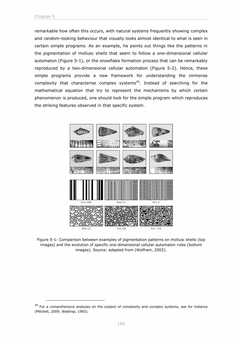
Chapter 5
160
remarkable how often this occurs, with natural systems frequently showing complex
and random-looking behaviour that visually looks almost identical to what is seen in
certain simple programs. As an example, he points out things like the patterns in
the pigmentation of mollusc shells that seem to follow a one-dimensional cellular
automaton (Figure 5-1), or the snowflake formation process that can be remarkably
reproduced by a two-dimensional cellular automaton (Figure 5-2). Hence, these
simple programs provide a new framework for understanding the immense
complexity that characterise complex systems26. Instead of searching for the
mathematical equation that try to represent the mechanisms by which certain
phenomenon is produced, one should look for the simple program which reproduces
the striking features observed in that specific system.
Figure 5-1: Comparison between examples of pigmentation patterns on mollusc shells (top
images) and the evolution of specific one-dimensional cellular automaton rules (bottom
images). Source: adapted from (Wolfram, 2002).
26
For a comprehensive analyses on the subject of complexity and complex systems, see for instance
(Mitchell, 2009; Waldrop, 1993).
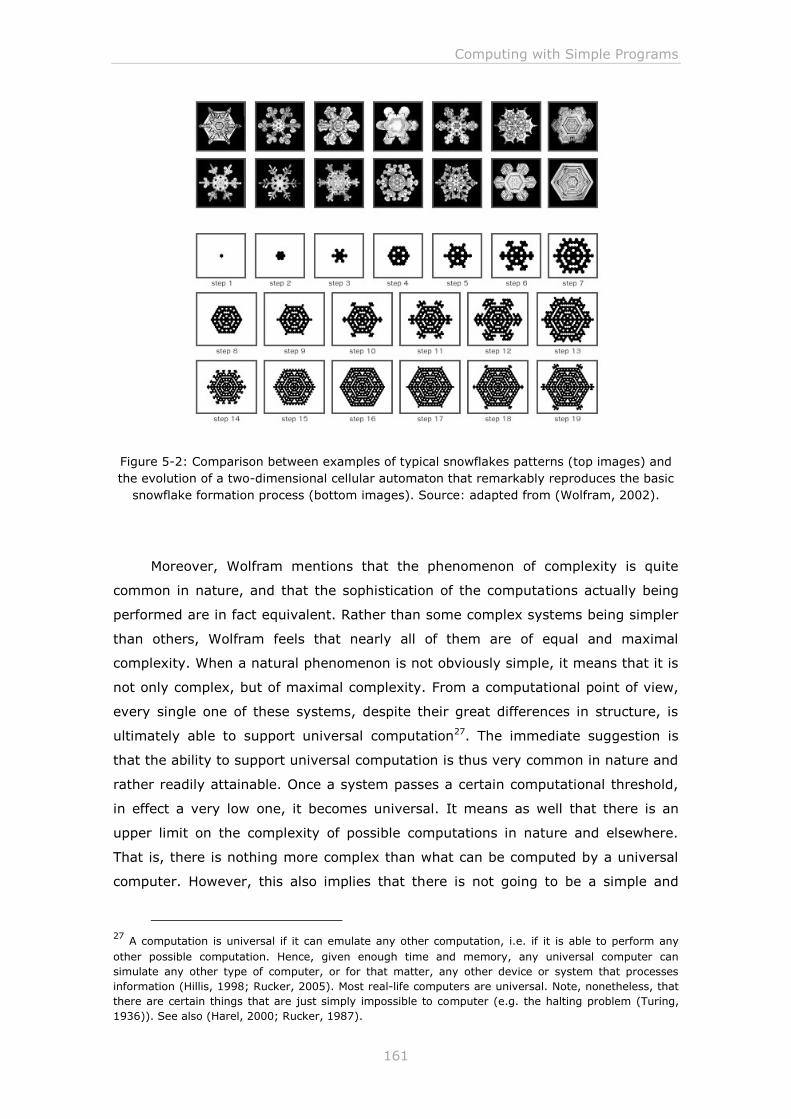
Computing with Simple Programs
161
Figure 5-2: Comparison between examples of typical snowflakes patterns (top images) and
the evolution of a two-dimensional cellular automaton that remarkably reproduces the basic
snowflake formation process (bottom images). Source: adapted from (Wolfram, 2002).
Moreover, Wolfram mentions that the phenomenon of complexity is quite
common in nature, and that the sophistication of the computations actually being
performed are in fact equivalent. Rather than some complex systems being simpler
than others, Wolfram feels that nearly all of them are of equal and maximal
complexity. When a natural phenomenon is not obviously simple, it means that it is
not only complex, but of maximal complexity. From a computational point of view,
every single one of these systems, despite their great differences in structure, is
ultimately able to support universal computation27. The immediate suggestion is
that the ability to support universal computation is thus very common in nature and
rather readily attainable. Once a system passes a certain computational threshold,
in effect a very low one, it becomes universal. It means as well that there is an
upper limit on the complexity of possible computations in nature and elsewhere.
That is, there is nothing more complex than what can be computed by a universal
computer. However, this also implies that there is not going to be a simple and
27
A computation is universal if it can emulate any other computation, i.e. if it is able to perform any
other possible computation. Hence, given enough time and memory, any universal computer can
simulate any other type of computer, or for that matter, any other device or system that processes
information (Hillis, 1998; Rucker, 2005). Most real-life computers are universal. Note, nonetheless, that
there are certain things that are just simply impossible to computer (e.g. the halting problem (Turing,
1936)). See also (Harel, 2000; Rucker, 1987).
Chapter 5
162
rapidly running computation that can emulate the natural world much faster that it
happens (Rucker, 2005; Wolfram, 2002).
Wolfram approaches various fields of science from the perspective of simple
programs, namely mathematics, physics, biology, fluid dynamics, artificial
intelligence, artificial life, chaos theory, complexity theory, economics,
consciousness, extra-terrestrial intelligence, and, of course, computer science. He
goes to the point of speculating that there is a “simple program which, if run for
long enough, would reproduce our universe in every detail” (Wolfram, 2002: 465) -
the ultimate model for the universe whose computations are the source of
everything that exists28. It is worth mentioning that the ideas and claims presented
in “A New Kind of Science” are far from consensual, being the target of scrutiny by
various scholars (see (Bailey, 2002; Kadanoff, 2002; Kurzweil, 2002; Mitchell,
2002)).
Considering the framework of this thesis, the core idea to retain is the
inherent potential of simple programs such as cellular automata in performing
complex computations in a non-traditional way. Systems with extremely simple
underlying rules can indeed produce complex outcomes and once a certain
threshold for complex behaviour has been reached, making the underling rules of a
system more complex does not ultimately lead to more complex overall behaviours.
From an aesthetical point of view, cellular automata provide an interesting way to
produce new forms of images that are capable of changing interactively (spatial
images).
5.2 The basics behind cellular automata
Cellular Automata (see for instance, (Toffoli and Margolus, 1987; Wolfram,
1983, 2002)) are discrete dynamical systems consisting of a uniform grid (or
lattice) of simple identical components, commonly called cells. The overall structure
can be viewed as a parallel processing device since the system has no central
controller and the communication between constituent cells is limited to local
interaction. Time advances in a succession of discrete steps and at each time
instance each individual cell exists in a specific state from a finite number of overall
possible states (for example, in the simplest possible cellular automata
28
The idea that the universe might be like a cellular automaton was in fact originally suggested by
Konrad Zuse as early as 1967 (Schmidhuber, 2002; Zuse, 1970). Likewise, Edward Fredkin theorised the
same concept, though some years later, before becoming acquainted with the work of Zuse (Fredkin,
1992; Wright, 1988).
Computing with Simple Programs
163
configuration two states are considered: on and off). The state of each individual
cell over time is determined based on the states of its local neighbour’s cells at the
preceding time step according to the application of a finite set of pre-determined
transition rules (also known as local rules) to the system. The dynamics of the
system results from repeatedly implementing the transition rules to every cell on
the grid. The rules can be represented in numerous different ways, from a set of IF-
THEN statements to a formula or a lookup table. Totalistic rules are those in which
the new state of a cell depends only on the average of the previous states of its
neighbours as well as on its own previous state. The best known two-dimensional
totalistic cellular automaton is the Game of Life (see Box 5-1).
Normally, the transition rules are applied simultaneously to every cell, i.e.
there is a global clock that dictates the pace of all local processes in the system,
and are identical for all cells. Even so, there are examples of asynchronous cellular
automata (Capcarrere, 2002; Cornforth et al., 2003; Ingerson and Buvel, 1984;
Nehaniv, 2003; Schönfisch and de Roos, 1999; Zielonka, 1987)29, where the state
of each cell is updated sequentially in such a way that the new state of a cell
influences the calculation of the state of neighbouring cells. The update sequence in
which the cells are considered can be described as either random or ordered.
Common employed approaches include (Cornforth et al., 2005): (a) the clocked
scheme, where each cell has its own independent timer, so that updating is
autonomous and proceeds at different rates for different cells; (b) the self-sync
scheme, similar to the clocked scheme, but the period of each timer is adjusted
after an update so as to more closely match the period of other cells in its
neighbourhood; (c) the cyclic scheme, where at each time step a cell is chosen
according to a fixed update order, which was decided at random during the
initialisation of the system; (d) the random independent scheme, where one cell is
randomly selected for update at each time step; and (e) the random order scheme,
where all cells are updated in a random order at each time step. Likewise, there are
examples of cellular automata where the transition rules are not identical for every
cell (i.e. each cell may contain a different rule). These are commonly called hybrid
or non-uniform cellular automata (Dennunzio et al., 2012; Dogaru, 2009; Sipper,
1994). In these particular cases of cellular automata, there is a collection of
transition rules that are applied according to the position of the cell.
One of the most fundamental properties of cellular automata is the
dimensional arrangement of the lattice on which the system is computed. In theory,
29
It is argued that the synchronous approach is not realistic from a biological point of view since there is
no accurate evidence of global synchronization in nature (Capcarrere, 2002; Cornforth et al., 2003).
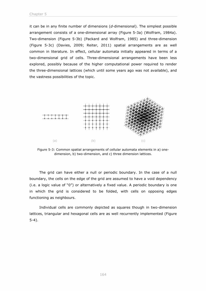
Chapter 5
164
it can be in any finite number of dimensions (d-dimensional). The simplest possible
arrangement consists of a one-dimensional array (Figure 5-3a) (Wolfram, 1984a).
Two-dimension (Figure 5-3b) (Packard and Wolfram, 1985) and three-dimension
(Figure 5-3c) (Davies, 2009; Reiter, 2011) spatial arrangements are as well
common in literature. In effect, cellular automata initially appeared in terms of a
two-dimensional grid of cells. Three-dimensional arrangements have been less
explored, possibly because of the higher computational power required to render
the three-dimensional lattices (which until some years ago was not available), and
the vastness possibilities of the topic.
Figure 5-3: Common spatial arrangements of cellular automata elements in a) one-
dimension, b) two-dimension, and c) three dimension lattices.
The grid can have either a null or periodic boundary. In the case of a null
boundary, the cells on the edge of the grid are assumed to have a void dependency
(i.e. a logic value of “0”) or alternatively a fixed value. A periodic boundary is one
in which the grid is considered to be folded, with cells on opposing edges
functioning as neighbours.
Individual cells are commonly depicted as squares though in two-dimension
lattices, triangular and hexagonal cells are as well recurrently implemented (Figure
5-4).
(a) (b) (c)
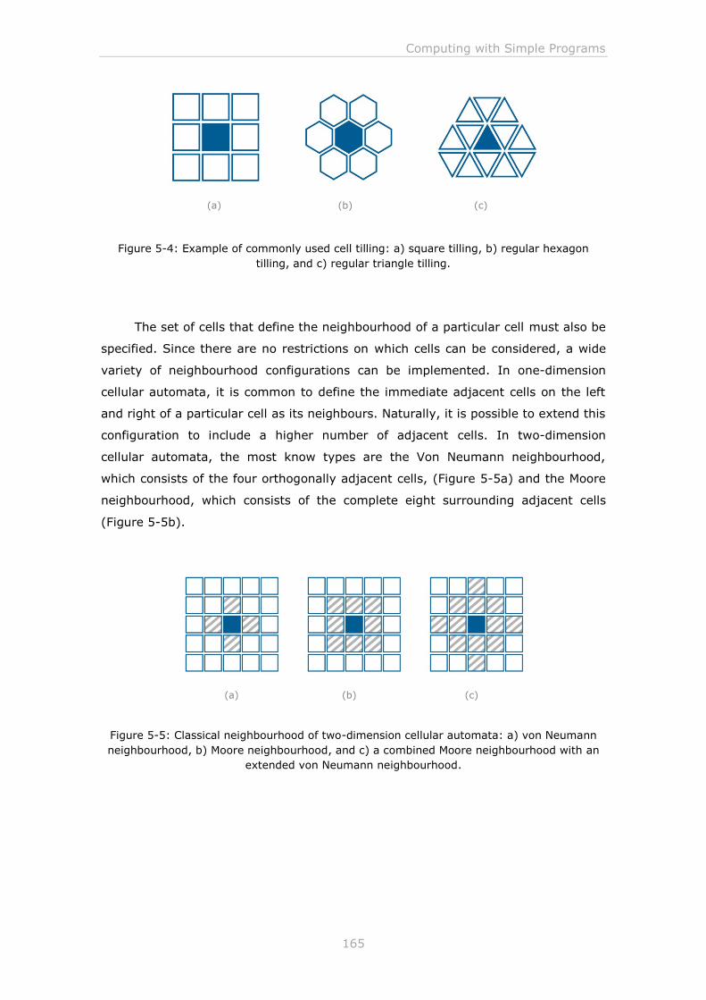
Computing with Simple Programs
165
Figure 5-4: Example of commonly used cell tilling: a) square tilling, b) regular hexagon
tilling, and c) regular triangle tilling.
The set of cells that define the neighbourhood of a particular cell must also be
specified. Since there are no restrictions on which cells can be considered, a wide
variety of neighbourhood configurations can be implemented. In one-dimension
cellular automata, it is common to define the immediate adjacent cells on the left
and right of a particular cell as its neighbours. Naturally, it is possible to extend this
configuration to include a higher number of adjacent cells. In two-dimension
cellular automata, the most know types are the Von Neumann neighbourhood,
which consists of the four orthogonally adjacent cells, (Figure 5-5a) and the Moore
neighbourhood, which consists of the complete eight surrounding adjacent cells
(Figure 5-5b).
Figure 5-5: Classical neighbourhood of two-dimension cellular automata: a) von Neumann
neighbourhood, b) Moore neighbourhood, and c) a combined Moore neighbourhood with an
extended von Neumann neighbourhood.
(a) (b) (c)
(a) (b) (c)
Chapter 5
166
Box 5-1: John Conway’s “Game of Life”.
Game of Life
The “Game of Life”, or simply “Life”, is a two-dimension cellular automaton
that was devised by the mathematician John Conway. It is the most widely known
example of cellular automata, having reach an immediate popularity when it was
first mentioned by Martin Gardner in his monthly column "Mathematical Games" of
the October 1970 issue of Scientific American (Gardner, 1970). The overall
excitement was primarily due to the fascinating patterns and intricate behaviours
that emerged from the very simple rules behind the computations.
In the Game of Life, individual cells can have either the value of 0 or 1 bit,
denoting respectively if the cell is dead or alive. It is a totalistic cellular automaton
meaning that the new state of a cell depends only on the average of the previous
values of its neighbours as well as on its own previous value. The neighbourhood
of each cell consisting of the eight surrounding adjacent cells (Moore
neighbourhood). Likewise cells are described as being alive or dead, the Game of
Life rules (Figure 5-6) are as well commonly phased in terms of life processes:
- A dead cell becomes alive at the next time step when that cell has exactly
three live neighbours (birth). Otherwise a dead cell stays dead.
- A live cell with exactly two or three live neighbours stays alive at the next
time step (survival). Otherwise it dies of loneliness (cell with fewer than
two live neighbours) or overcrowding (cell with more than three live
neighbours).
The Game of Life balances these tendencies, making it difficult to figure
whether a pattern will die out completely, form a stable population, or grow
forever.
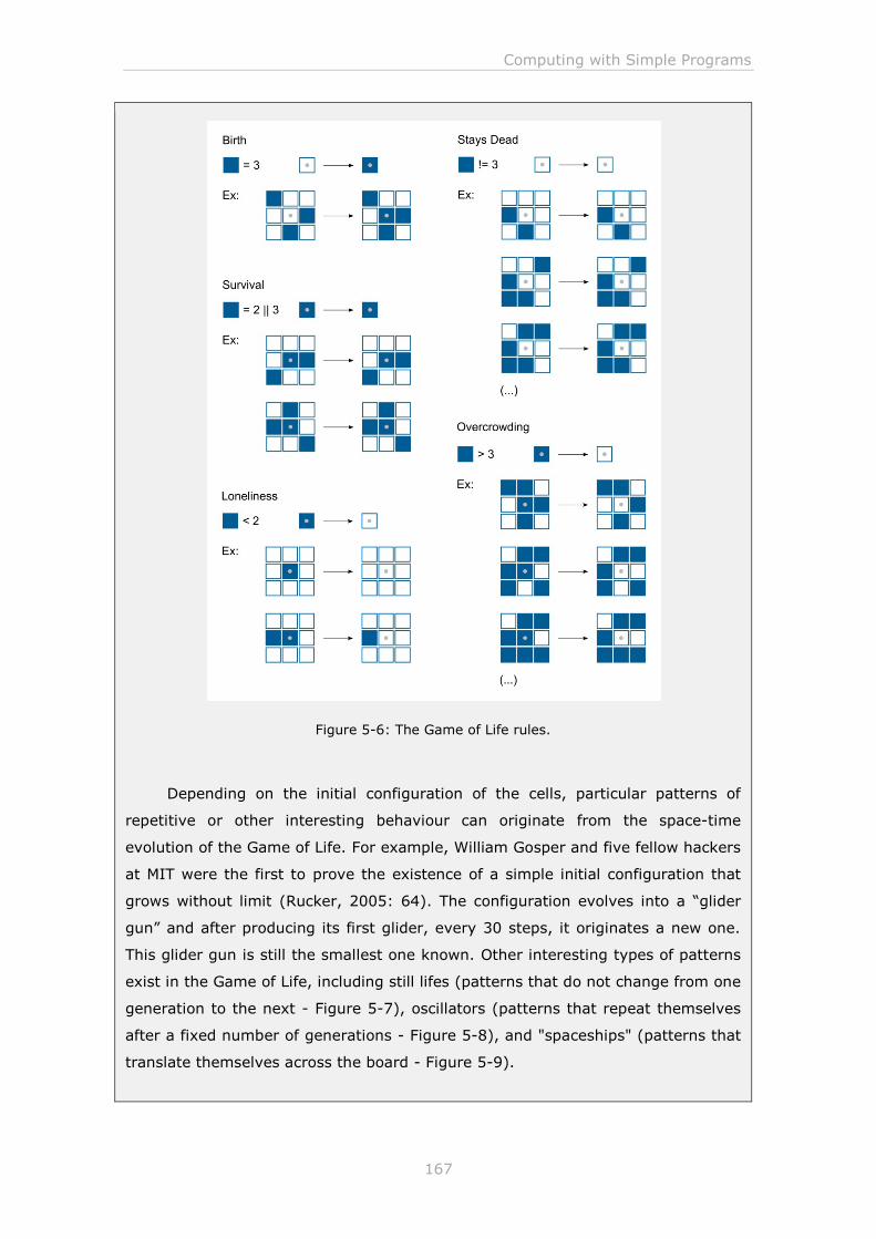
Computing with Simple Programs
167
Figure 5-6: The Game of Life rules.
Depending on the initial configuration of the cells, particular patterns of
repetitive or other interesting behaviour can originate from the space-time
evolution of the Game of Life. For example, William Gosper and five fellow hackers
at MIT were the first to prove the existence of a simple initial configuration that
grows without limit (Rucker, 2005: 64). The configuration evolves into a “glider
gun” and after producing its first glider, every 30 steps, it originates a new one.
This glider gun is still the smallest one known. Other interesting types of patterns
exist in the Game of Life, including still lifes (patterns that do not change from one
generation to the next - Figure 5-7), oscillators (patterns that repeat themselves
after a fixed number of generations - Figure 5-8), and "spaceships" (patterns that
translate themselves across the board - Figure 5-9).
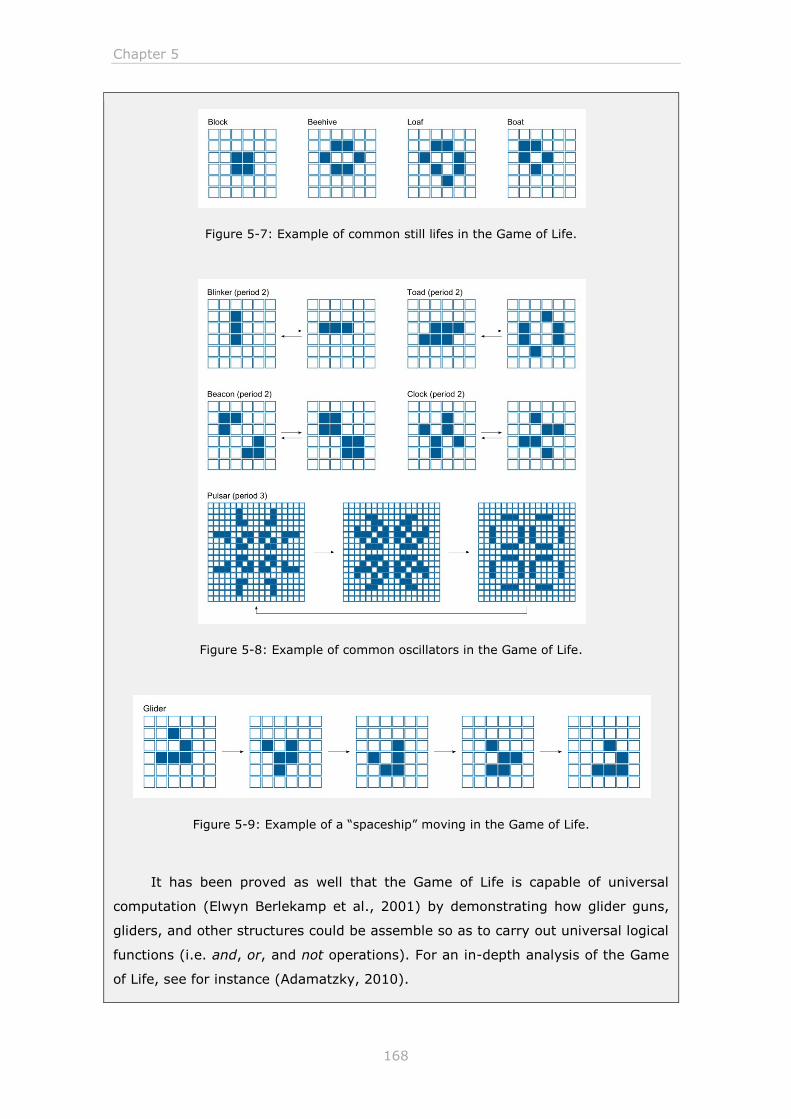
Chapter 5
168
Figure 5-7: Example of common still lifes in the Game of Life.
Figure 5-8: Example of common oscillators in the Game of Life.
Figure 5-9: Example of a “spaceship” moving in the Game of Life.
It has been proved as well that the Game of Life is capable of universal
computation (Elwyn Berlekamp et al., 2001) by demonstrating how glider guns,
gliders, and other structures could be assemble so as to carry out universal logical
functions (i.e. and, or, and not operations). For an in-depth analysis of the Game
of Life, see for instance (Adamatzky, 2010).
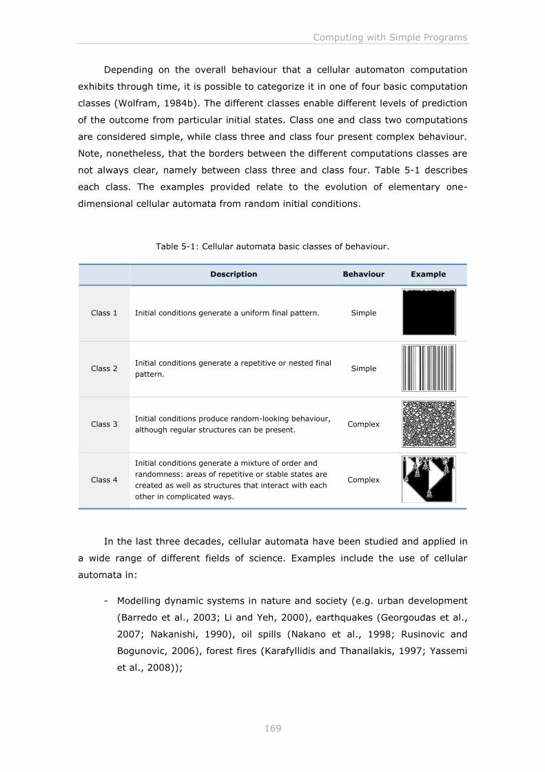
Computing with Simple Programs
169
Depending on the overall behaviour that a cellular automaton computation
exhibits through time, it is possible to categorize it in one of four basic computation
classes (Wolfram, 1984b). The different classes enable different levels of prediction
of the outcome from particular initial states. Class one and class two computations
are considered simple, while class three and class four present complex behaviour.
Note, nonetheless, that the borders between the different computations classes are
not always clear, namely between class three and class four. Table 5-1 describes
each class. The examples provided relate to the evolution of elementary one-
dimensional cellular automata from random initial conditions.
Table 5-1: Cellular automata basic classes of behaviour.
Description Behaviour Example
Class 1 Initial conditions generate a uniform final pattern. Simple
Class 2 Initial conditions generate a repetitive or nested final
pattern. Simple
Class 3 Initial conditions produce random-looking behaviour,
although regular structures can be present. Complex
Class 4
Initial conditions generate a mixture of order and
randomness: areas of repetitive or stable states are
created as well as structures that interact with each
other in complicated ways.
Complex
In the last three decades, cellular automata have been studied and applied in
a wide range of different fields of science. Examples include the use of cellular
automata in:
- Modelling dynamic systems in nature and society (e.g. urban development
(Barredo et al., 2003; Li and Yeh, 2000), earthquakes (Georgoudas et al.,
2007; Nakanishi, 1990), oil spills (Nakano et al., 1998; Rusinovic and
Bogunovic, 2006), forest fires (Karafyllidis and Thanailakis, 1997; Yassemi
et al., 2008));
Chapter 5
170
- Modelling physical systems (e.g. fluid dynamics (Frisch et al., 1986;
Wolfram, 1986), gas behaviour (Boon et al., 1996; Zahedi Sohi and
Khoshandam, 2012)),
- Modelling chemical systems (e.g. first- and second-order kinetic
phenomena (Kier et al., 2000; Seybold et al., 1997), Belousov–
Zhabotinsky reaction (Gerhardt and Schuster, 1989; Markus and Hess,
1990))
- Modelling biological systems (e.g. predator-prey dynamics (Droz and
Pȩkalski, 2001; Pekalski, 2004), immunology (Chowdhury et al., 1990;
Sieburg et al., 1990), cell grow (Alarcón et al., 2003; Ermentrout and
Edelstein-Keshet, 1993), pigmentation formation (Gunji, 1990; Markus and
Kusch, 1995));
- Idealizations of massively parallel, non-centralized computation (Hansen,
1993; Spezzano and Talia, 1999);
- Cryptography as generators of random numbers (Nandi et al., 1994;
Seredynski et al., 2004).
- Animation (e.g. clouds (Dobashi et al., 2000; Miyazaki et al., n.d.) and
water waves (Wang et al., 2003))
Comprehensive surveys highlighting the theory and applications of cellular
automata can be found in (Ganguly et al., 2003; Kari, 2005; Kutrib et al., 1997;
Mitchell, 1998).
5.3 Computing with pictorial entities
Most computations are primarily done based on numerical entities due to
these being easily interpreted, written and manipulated (Nickerson, 1988).
However, in our daily life, we mainly use linguistic and pictorial entities to describe
the world. The use of linguistic (Zadeh, 1975) and pictorial (Camara et al., 1994)
entities in computation allows the shift from strictly quantitative variables into more
qualitative and distributed representations of reality. Indeed, pictorials entities can
be a powerful and efficient mean to represent concepts and ideas, overcoming as
well existing language barriers.
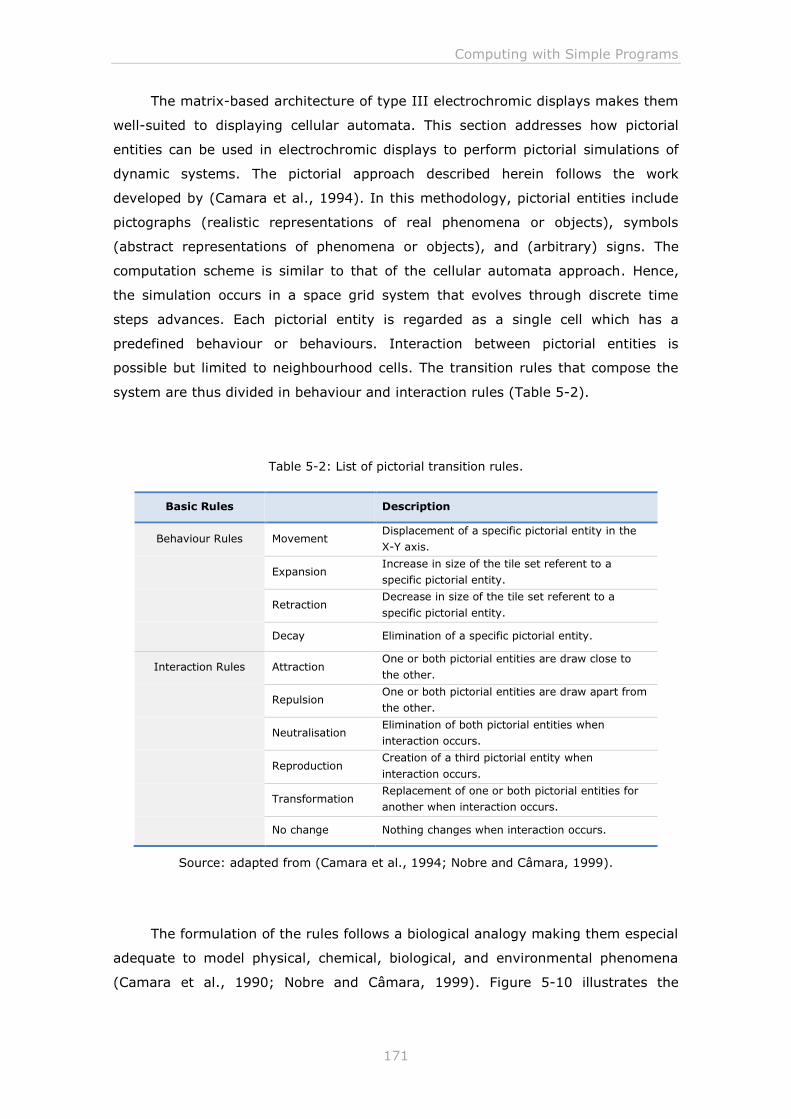
Computing with Simple Programs
171
The matrix-based architecture of type III electrochromic displays makes them
well-suited to displaying cellular automata. This section addresses how pictorial
entities can be used in electrochromic displays to perform pictorial simulations of
dynamic systems. The pictorial approach described herein follows the work
developed by (Camara et al., 1994). In this methodology, pictorial entities include
pictographs (realistic representations of real phenomena or objects), symbols
(abstract representations of phenomena or objects), and (arbitrary) signs. The
computation scheme is similar to that of the cellular automata approach. Hence,
the simulation occurs in a space grid system that evolves through discrete time
steps advances. Each pictorial entity is regarded as a single cell which has a
predefined behaviour or behaviours. Interaction between pictorial entities is
possible but limited to neighbourhood cells. The transition rules that compose the
system are thus divided in behaviour and interaction rules (Table 5-2).
Table 5-2: List of pictorial transition rules.
Basic Rules Description
Behaviour Rules Movement Displacement of a specific pictorial entity in the
X-Y axis.
Expansion Increase in size of the tile set referent to a
specific pictorial entity.
Retraction Decrease in size of the tile set referent to a
specific pictorial entity.
Decay Elimination of a specific pictorial entity.
Interaction Rules Attraction One or both pictorial entities are draw close to
the other.
Repulsion One or both pictorial entities are draw apart from
the other.
Neutralisation Elimination of both pictorial entities when
interaction occurs.
Reproduction Creation of a third pictorial entity when
interaction occurs.
Transformation Replacement of one or both pictorial entities for
another when interaction occurs.
No change Nothing changes when interaction occurs.
Source: adapted from (Camara et al., 1994; Nobre and Câmara, 1999).
The formulation of the rules follows a biological analogy making them especial
adequate to model physical, chemical, biological, and environmental phenomena
(Camara et al., 1990; Nobre and Câmara, 1999). Figure 5-10 illustrates the
Chapter 5
172
application of the behaviour and interaction rules in a two-dimensional spatial
arrangement.
Figure 5-10: Exemplification of the pictorial simulation behaviour and interaction Rules.
5.3.1 Implementation in electrochromic display
The implementation of the pictorial simulation approach was envisaged in a
multi-layer architecture based on a series of interconnected modules of stackable
electrochromic displays (Figure 5-11).
Computing with Simple Programs
173
Figure 5-11: Architecture of the pictorial simulation environment.
The system is divided in a two-level hierarchical structure. The base level
encodes the overall space and time structure of the system such as the type of
boundary (cyclic or null), the type of neighbourhood (von Neumann, Moore or
other), and the global clock (synchronous or asynchronous). It is formed by a
single layer representing a particular simulation environment.
The top level provides the logic for the simulation. It encodes the
specifications of the components that form the system. It is composed by one or
more layers, each representing a specific pictorial entity with a pre-determined set
of behaviour and interaction rules. Each layer can function independently from the
others but also in interaction. Hence, when only a pictorial entity layer is
implemented in the system, the simulation will be based essentially on the
behaviour rules created for that specific pictorial entity. In contrasts, when multiple
layers are stacked together, i.e. connected to one another, the simulation will be
Chapter 5
174
based both on the behaviour rules of each pictorial entity but also on the interaction
rules. This allows the engineering of specific interactions between certain pictorial
entities.
The system is idealised to allow the layers to be changed easily. Also,
additional ones can be added to the system at any given moment, enabling new
pictorial entities to be incorporated to the simulation. The crucial element of this
architecture is that all information and instructions must be clearly defined and
separated according to the hierarchical structure of the system. The system
architecture was replicated in a computer simulation. The code diagram for system
is provided in Annex I.
Pictorial simulation can be applied to various spatial simulation problems
(Camara et al., 1990, 1994; Nobre and Câmara, 1999). As mentioned above, the
formulation of the rules follows a biological analogy making them especially
adequate to model physical, chemical, biological, and environmental phenomena.
Typical uses include the modelling of forest fires, floods, oil spills, and predator-
prey dynamics. From an educational application standpoint view it provides a
tangible way for experimenting with complex systems (and acquire knowledge)
using straightforward pictorial entities and intuitive transition rules.
5.4 Concluding remarks
Cellular automata are a fascinating type of computation. Despite of their
underlying simple structure, cellular automata are capable of producing outcomes
that are far from simple. One of the obvious attractions of cellular automata is the
complex and often beautiful visual patterns that they can generate. The number of
interesting configurations that can be made from these elements is immense. Other
appeal of cellular automata is the potential to simulate different sophisticated
natural phenomena. By using the type of rules embodied in cellular automata it is
possible to capture a vast range of essential mechanisms in physical, chemical, and
biological systems. The Game of Life is one of the best know cellular automata. It is
characterised by generating a great number of structures such as oscillators and
“spaceships” capable of producing interesting behaviour on the boundary between
stability and chaos. With proper initial conditions it is also capable of simulating any
given computation. In fact, there are cellular automata systems whose rules are
simple enough to be described in a few sentences that are nevertheless capable of
universal computation (e.g. rule 110 (Cook, 2004)).
Computing with Simple Programs
175
The matrix-based architecture of type III electrochromic displays naturally
suggests its use with cellular automata. A clear analogy can be made between the
individual cells in cellular automata and the pixels in an image, with the
particularity that the dynamic nature of cellular automata can be used to animate
the static pixels. Hence, cellular automata can be used to produce interesting
patterns and images in electrochromic displays, even with a rather small number of
pixels. On the other hand, it is somehow laborious to design cellular automata rules
to have a specific behaviour or to produce a specific pattern, unless the rules for
that specific outcome are already known.
The use of pictorial entities as pixel elements provides a different approach to
the presentation of visual information. The association of specific behaviour and
interaction rules extended with cellular automata formulation to unique pictorial
entities enables in turn an object oriented simulation of natural systems with
inherent temporal and spatial dimensions. The approach presented is based on a
multi-layer architecture of stackable electrochromic displays. It intends to provide a
tangible way for experimenting with complex systems using intuitive transition
rules and obvious pictorial entities. The real engineering challenges lie in the design
and development of the necessary hardware.

Chapter 5
176
Conclusions and Future Research
177
6 Conclusions and Future Research
The research work undertaken in this thesis is based on the premise that
computers should be invisible. Its use and presence should be so natural that they
would become part of our surroundings and daily activities. Microcomputers would
be integrated into everyday objects, augmenting a physical object’s original use-
value with a new set of digital functionalities.
The advances made in microelectronics and communications technology in the
last two decades have pushed the technical vision of Ubiquitous Computing into the
realm of the possible. Computers have become mobile and ever connected to the
internet. Tablet computers or more clearly e-book readers are gradually
overcoming the paradigm of the general-purpose personal computer in favour of
small, specialised digital devices that are entering our lifestyle. However, we are
not yet in the presence of a truly invisible computer. It is evident that smaller,
faster and cheaper microelectronics as well as better interconnectivity between
devices are a fundamental aspect of the vision of Ubiquitous Computing, but
materials capable of levelling the integration of the physical and digital worlds are
as well essential.
Printed Electronics is presented as a ground-breaking new type of electronics
that are able to enhance the current state of Ubiquitous Computing. It promises the
mass production of low-cost, lightweight, thin and flexible digital devices free from
form factors. The idea behind is to use conventional printing technologies to
produce passive and active electronic components in a wide array of substrates
through the printing of electro-optical functional inks. The possibility of
incorporating the concepts behind Printed Electronics with 3D printing is as well
attractive. Complete digital devices and interactive objects could be created as a
single part rather than as a case that encloses the circuit boards and individual
electronic components. For instance, sensing and display elements could be directly
embedded in the mechanical structure of the object being created instead of being
assembled separately and incorporated afterwards.
Chapter 6
178
The idea that all these technologies will be available to the general public is as
well a compelling one. Nowadays, there are already numerous individuals that are
taking advantage of the potential of digital fabrication technologies not only to
create the things that they desire and need, rather than using what someone else
thought they needed, but more importantly to solve specific problems that directly
affects them. Indeed, Personal Fabrication is empowering individuals by giving
them the control over technology and its development, whilst fulfilling their desires.
Making Printed Electronics technologies available to the general public can
further pave the way for the development of a technological world shaped by its
users and a user-driven reality of Ubiquitous Computing. It will encourage new
ideas and products to come to life whilst giving end-users the ability to develop
their own embedded digital devices. Likewise the internet ended up being shaped
by its users and its utility adapted by each one of us, an open Internet of Things
might as well be produced by all of us.
The realisation of the vision of Ubiquitous Computing is naturally dependent
on the development of various technologies. For example, advances in wireless
communications, energy storage, human-to-machine interfaces, sensors and digital
display screens are of particular significance. In this thesis it was given a clear
emphasis to the latest. Visual communication has always played an important role
in human societies and nowadays, more than ever, is often used as a method of
choice for conveying information.
In order to achieve a truly invisible computer, new ways to provide and
present digital information have to be implemented. These must be able to present
dynamic information and be easily incorporated into objects. Electrochromic
displays have the potential to enable exciting novel forms of visual content than can
be used to not only to entertain but also to inform and engage audiences to take
action. From a point of view of creativity, it becomes possible to create hybrid
contents that mix the traditional graphic print look and feel with features from the
digital area, such as animated and readily updatable content. The effective use of
such technology is nonetheless, subject to the strategic deployment of their unique
features for a given situation. Different purposes can represent different
architectures, with different complexities. Moreover, it should be taken into account
that the technology is only an enabler. Careful attention must be given as well to
the nature and presentation of the content which must be relevant and interesting
to the audience at hand. As in traditional visual communication printed approaches,
design considerations about the legibility, readability, typography, and imagery of
the content must be taken into account in order to deliver an effective message.
Conclusions and Future Research
179
These elements can be used to either emphasize important information or de-
emphasize more trivial details. The possibility to add animations and movement to
such elements means that not only new compositions and arrangements can be
exploited but as well that all the elements have to be carefully integrated. In sum,
a well-designed display can only be used to give a strong and clear message that
successfully will draw attention, raise awareness, provide guidance, or simple
entertain, if it delivers the appropriate content for the audience in question.
Aesthetics and function have to be combined to provide a unique identity.
The proposed classification for electrochromic displays based on the type of
architecture/content intended to illustrate the potential of these for presenting
dynamic information beyond the traditional alphanumeric seven-segment
arrangements and dot-matrix arrangements. It is composed by three main
categories (type I to type III), with each category in its turn being divided in two
sub-types (A and B). The examples developed for each type of architecture/content
illustrate how these can be implemented as simple, task-specific applications
following an end-user fabrication process. They all emphasize interaction and visual
actuation, using the minimal hardware components. Likewise to what would be
expected in a Personal Fabrication approach, all the materials and electronic
components used to make the devices are commercially available online or in any
electronics specialty store.
The complexity of the display architecture increases from type I to type III,
likewise the ability to present dynamic visual content. Type A refers to the basic
architecture/content, namely, for type I-A, the direct addressing of a pre-
determined image; for a type II-A, the direct addressing of a set of geometric
abstract segments that when combined form specific pre-determined visual
elements; and for a type III-A, the matrix addressing of geometric abstract pixels
capable of form bitmap images. Type B represents an enhancement in terms of
content to the basic structure. In type I-B, the pre-determined image is segmented
so its individual parts can be activated and animated separately; while in type II-B,
the use of pictorial images (e.g. icons or glyphs) instead of abstract geometric
picture elements not only enables new types of content but as well can provide a
more visually stimulating approach and effective communication. Type III-B further
explores the use of pictorial elements as pixels by associating to each pixel a
specific meaning that influences the overall visual content of the display. It is
highlighted its use as an interface for pictorial based simulations through extended
cellular automata formulations.
Chapter 6
180
Indeed, cellular automata are introduced here as a simple computation model
capable of producing highly complex behaviour and visually interesting patterns.
The spatial structure of cellular automata is equivalent to the matrix-based
architecture of type III electrochromic displays, with the pixels of the display
mirroring the individual cells of a cellular automaton. As such, the dynamic process
of cellular automata can be explored to create dynamic visual content in
electrochromic displays, though its use goes well beyond the creation of visually
interesting patterns.
The ability to have pictorial elements as pixels in electrochromic displays
instead of abstract geometric figures is further explored through the association of
specific cellular automata-based behaviour and interaction rules to unique pictorial
entities. The pictorial simulation approach followed attempts to provide an object
oriented simulation of natural systems with inherent temporal and spatial
dimensions. Its applicability in real-world, in the context of this thesis, was
conceptualised through the development of a task-specific device based on a multi-
layer architecture of stackable electrochromic displays. The main aim was to
provide a simple and tangible way of experimenting with complex systems using
intuitive and clear transition rules and pictorial entities. Ultimately, it is expected
that it will lead to more ideas for applications and more sophisticated requirements
for it. The main innovation of the proposed system relies in the integration of the
different components. Even though the final device was not fully developed, due to
current technology constrains, the technology concept and application were
formulated, and experimentation and validation of the separate elements was done.
The aim of this thesis was to explore and demonstrate new possibilities for
task-specific, low computation interactive devices. The various experiences and
applications developed demonstrated that the technical universe explored (i.e. the
exploit of printed circuits and electrochromic displays) offers new creative
opportunities for inexpensive, flexible, visual communication digital devices. It also
opens the doors for further research on the topic.
Electrochromic displays still require various improvements in ordered to
achieve their expected potential. There is still a sizable gap between the theoretical
performance of electrochromic displays and the actual working capabilities.
Improvements in the resolution of the displays, contrast and lifespan are required.
The limited variety of available colours and the slow response times are also
observable drawbacks in certain applications. Further research is required as well in
the development of adequate matrix-addressing control units and operating
schemes. Passive matrix addressing schemes have the tendency to originate
Conclusions and Future Research
181
voltage leaks between neighbourhood pixels of active pixels, resulting in the
colouration of undesired elements (the crosstalk effect). In turn, active-matrix
addressing schemes are more complex and costly to manufacture that passive-
matrix addressing electrochromic displays. Further investigation in terms of real
world applications for electrochromic displays aimed at the presentation of dynamic
visual information is also necessary. Most applications developed so far are either
prototypes or technology showcases. It is necessary to deploy them in real world
contexts and analyse how the public reacts to it.
From a Personal Fabrication ideal point of view, it would be interesting to
explore and further develop fabrication technologies and processes that could make
accessible Printed Electronics to the general public. Nowadays, Printed Electronics
technologies are mainly available to specialised companies and R&D institutes. In
an attempt to change this tendency, various companies launched recently
crowdfunding campaigns to make available their Printed Electronics products to
everyone. For example, Ynvisible successfully funded Printoo30 on May 2004, an
open-source printed electronic prototyping platform of paper-thin circuit boards and
modules, and AgIC31, named after Ag Inkjet Circuit, funded on April 2014,
transforms home inkjet printers into Printed Electronic circuit board manufacturing
equipment. Another interesting example is Circuit Stickers32, a set of adhesive peel-
and-stick electronics for crafting circuits that can be used in combination with
conductive materials such as conductive paint or thread to build interactive projects
without any complicated equipment or programming skills. All these examples
illustrate solutions aimed at facilitating the fabrication process of electronic circuits
whilst enabling electronics to be integrated in a range of non-traditional material.
They also have the potential to be an effective education tool for the general public.
More approaches of this nature would be more than welcome.
Last but not least, it would be interesting to further explore how the simplicity
of cellular automata can be exploited not only to create interesting visual patterns
in electrochromic displays but as well as a way to operate ubiquitous computing
devices. The proposed prototype is a very specific example idealised for the
simulation of dynamic systems that also needs to be further developed to bring the
concept towards a higher technology readiness level. The basic technological
components for such device are all identified but still need to be integrated with
30 http://www.printoo.pt 31 http://agic.cc/ 32 http://chibitronics.com/
Chapter 6
182
reasonably realistic supporting elements so they can be tested in a real world
environment.
In sum, the main contributions of this research work can be listed as:
- Contextualization of the potential of Printed Electronics and Personal
Fabrication in driving Ubiquitous Computing;
- Development of task-specific, visual information applications using direct
addressing and passive-matrix addressing electrochromic displays and
open source hardware;
- Systematization of visual content types in electrochromic displays;
- Reframing of the use of Pictorial Entities as a tangible way of
experimenting with complex systems through the use of matrix addressing
electrochromic displays.
References
183
7 References
Adamatzky A (2010) Game of Life Cellular Automata. Adamatzky A (ed.), London:
Springer London, Available from: http://link.springer.com/10.1007/978-1-
84996-217-9 (accessed 20 March 2014).
Aernouts T, Vanlaeke P, Poortmans J, et al. (2004) Polymer solar cells: screen
printing as a novel deposition technique. In: Heremans PL, Muccini M, and
Hofstraat H (eds), Proc. SPIE 5464, Organic Optoelectronics and Photonics, pp.
252–260, Available from:
http://proceedings.spiedigitallibrary.org/proceeding.aspx?articleid=846124 (accessed 17 April 2013).
Agnihotry SA, Nidhi, Pradeep, et al. (2000) Li+ conducting gel electrolyte for
electrochromic windows. Solid State Ionics, 136-137(1-2), 573–576, Available
from: http://linkinghub.elsevier.com/retrieve/pii/S0167273800003398
(accessed 23 August 2012).
Alarcón T, Byrne HM and Maini PK (2003) A cellular automaton model for tumour
growth in inhomogeneous environment. Journal of Theoretical Biology, 225(2),
257–274, Available from:
http://linkinghub.elsevier.com/retrieve/pii/S0022519303002443 (accessed 25
March 2014).
Albert JD, Comiskey B, Jacobson JM, et al. (2000) Multi-color electrophoretic displays and materials for making the same. USA: United States Patent.
Albert JD, Comiskey B, Jacobson JM, et al. (2001) Retroreflective electrophoretic displays and materials for making the same. USA: United States Patent.
Aliev a. . and Shin H. (2002) Image diffusion and cross-talk in passive matrix
electrochromic displays. Displays, 23(5), 239–247, Available from:
http://linkinghub.elsevier.com/retrieve/pii/S0141938202000525.
Allen M, Aronniemi M, Mattila T, et al. (2011) Contactless read-out of printed
memory. Microelectronic Engineering, 88(9), 2941–2945, Available from:
http://linkinghub.elsevier.com/retrieve/pii/S0167931711004503 (accessed 31 January 2013).
Alt PM and Pleshko P (1974) Scanning limitations of liquid-crystal displays. IEEE
Transactions on Electron Devices, 21(2), 146–155, Available from:
http://ieeexplore.ieee.org/lpdocs/epic03/wrapper.htm?arnumber=1477699 (accessed 13 August 2012).
Amundson K (2005) Electrophoretic Imaging Films for Electronic Paper Displays. In: Crawford G (ed.), Flexible flat panel displays, John Wiley & Sons.

184
Anderson C (2012) Makers: The New Industrial Revolution. London, UK: Random
House Business Books.
Andersson H, Rusu A, Manuilskiy A, et al. (2011) System of nano-silver inkjet
printed memory cards and PC card reader and programmer. Microelectronics
Journal, 42(1), 21–27, Available from:
http://linkinghub.elsevier.com/retrieve/pii/S0026269210002089 (accessed 25
February 2013).
Andersson P, Nilsson D, Svensson P-O, et al. (2002) Active Matrix Displays Based
on All-Organic Electrochemical Smart Pixels Printed on Paper. Advanced Materials, 14(20), 1460–1464.
Andersson P, Forchheimer R, Tehrani P, et al. (2007) Printable All-Organic
Electrochromic Active-Matrix Displays. Advanced Functional Materials, 17(16),
3074–3082, Available from: http://doi.wiley.com/10.1002/adfm.200601241 (accessed 19 July 2012).
Antinucci M, Chevalier B and Ferriolo A (1995) Development and characterisation of
electrochromic devices on polymeric substrates. Solar Energy Materials and
Solar Cells, 39(2-4), 271–287, Available from:
http://linkinghub.elsevier.com/retrieve/pii/092702489500064X (accessed 1 October 2012).
Argun A a., Aubert P-H, Thompson BC, et al. (2004) Multicolored Electrochromism
in Polymers: Structures and Devices. Chemistry of Materials, 16(23), 4401–
4412, Available from: http://pubs.acs.org/doi/abs/10.1021/cm049669l.
Argun AA, Cirpan A and Reynolds JR (2003) The First Truly All-Polymer
Electrochromic Devices. Advanced Materials, 15(16), 1338–1341, Available
from: http://doi.wiley.com/10.1002/adma.200305038 (accessed 4 August 2012).
Arimoto FS and Haven AC (1955) Derivatives of Dicyclopentadienyliron. Journal of
the American Chemical Society, 77(23), 6295–6297.
Arsenault AC, Puzzo DP, Manners I, et al. (2007) Photonic-crystal full-colour
displays. Nature Photonics, 1(8), 468–472, Available from:
http://www.nature.com/doifinder/10.1038/nphoton.2007.140 (accessed 3 December 2012).
AT&T Laboratories Cambridge (2002) The Active Badge System. AT&T Laboratories
Cambridge website.
Badila M, Brochon C, Hébraud A, et al. (2008) Encapsulation of TiO2 in poly(4-vinyl
pyridine)-based cationic microparticles for electrophoretic inks. Polymer,
49(21), 4529–4533, Available from:
http://linkinghub.elsevier.com/retrieve/pii/S0032386108006459 (accessed 28
November 2012).
Baetens R, Jelle BP and Gustavsen A (2010) Properties, requirements and
possibilities of smart windows for dynamic daylight and solar energy control in
buildings: A state-of-the-art review. Solar Energy Materials and Solar Cells,
Elsevier, 94(2), 87–105, Available from:
References
185
http://linkinghub.elsevier.com/retrieve/pii/S0927024809002992 (accessed 18
July 2012).
Bailey DH (2002) A Reclusive Kind of Science. Computing in Science and Engineering, 4(5), 79–81.
Bakker S, Hoven E van den and Eggen B (2010) Design for the Periphery. In:
Eurohaptics 2010: Proceedings of the special sympo- sium haptic and audio-visual stimuli, pp. 71–80.
Bamfield P and Hutchings MG (2010) Chromic Phenomena: Technological
Applications of Colour Chemistry. RSC Publishing.
Banzi M (2011) Getting Started with Arduino. 2nd Editio. O’Reilly Media / Make.
Barnes HA (1997) Thixotropy - A review. Journal of Non-Newtonian Fluid
Mechanics, 70(1-2), 1–33, Available from:
http://linkinghub.elsevier.com/retrieve/pii/S0377025797000049 (accessed 2 March 2013).
Barr MC, Rowehl JA, Lunt RR, et al. (2011) Direct Monolithic Integration of Organic
Photovoltaic Circuits on Unmodified Paper. Advanced Materials, 23(31), 3500–
3505, Available from: http://www.ncbi.nlm.nih.gov/pubmed/21739489 (accessed 15 February 2013).
Barredo JI, Kasanko M, McCormick N, et al. (2003) Modelling dynamic spatial
processes: simulation of urban future scenarios through cellular automata.
Landscape and Urban Planning, 64(3), 145–160, Available from:
http://linkinghub.elsevier.com/retrieve/pii/S0169204602002189 (accessed 22 April 2014).
Baucke FG. (1987) Electrochromic mirrors with variable reflectance. Solar Energy
Materials, 16(1-3), 67–77, Available from:
http://linkinghub.elsevier.com/retrieve/pii/0165163387900098 (accessed 28 July 2012).
Bauwens P, Monté A, Christiaens W, et al. (2009) Improved passive-matrix
multiplexability with a modular display and UTCP technology. Displays, 30(2),
71–76, Available from:
http://linkinghub.elsevier.com/retrieve/pii/S0141938208000851 (accessed 16 October 2012).
Beaujuge PM and Reynolds JR (2010) Color control in pi-conjugated organic
polymers for use in electrochromic devices. Chemical reviews, 110(1), 268–
320, Available from: http://www.ncbi.nlm.nih.gov/pubmed/20070115 (accessed 13 July 2012).
Beecher P, Servati P, Rozhin A, et al. (2007) Ink-jet printing of carbon nanotube
thin film transistors. Journal of Applied Physics, 102(4), 043710–7, Available
from: http://link.aip.org/link/JAPIAU/v102/i4/p043710/s1&Agg=doi (accessed
10 March 2013).
Bennett N (2012) Create innovative interactive paper apps by mixing graphic
design and printed electronics. Digital Arts, Available from:
http://www.digitalartsonline.co.uk/features/hacking-maker/create-innovative-
186
interactive-paper-apps-by-mixing-graphic-design-printed-electronics/
(accessed 26 April 2013).
Berzina Z (2011) Touche Me. Zane Berzina Website, Available from: http://www.zaneberzina.com/touchme.htm (accessed 18 January 2013).
Bird CL and Kuhn AT (1981) Electrochemistry of the viologens. Chemical Society
Reviews, 10(1), 49–82, Available from: http://xlink.rsc.org/?DOI=cs9811000049 (accessed 5 August 2012).
Birnstock J, Blaessing J, Hunze A, et al. (2002) Screen-printed passive matrix
displays and multicolor devices. In: Kafafi ZH (ed.), Proc. SPIE 4464, Organic
Light-Emitting Materials and Devices V, pp. 68–75, Available from:
http://proceedings.spiedigitallibrary.org/proceeding.aspx?articleid=891247 (accessed 17 April 2013).
Bliss A (2013) Printed electronics: the future at your fingertips. Computer Arts,
Available from: http://www.computerarts.co.uk/blog/printed-electronics-future-your-fingertips-133664 (accessed 26 April 2013).
Blue Spark (2011) Blue Spark Website. Blue Spark Technologies Website, Available from: http://www.bluesparktechnologies.com/ (accessed 25 February 2013).
Bohn J, Coroama V, Langheinrich M, et al. (2005) Social, economic, and ethical
implications of ambient intelligence and ubiquitous computing. In: Weber W,
Rabaey J, and Aarts E (eds), Ambient Intelligence, Springer-Verlag, pp. 5–29.
Bonfil Y, Brand M and Kirowa-Eisner E (2000) Trace determination of mercury by
anodic stripping voltammetry at the rotating gold electrode. Analytica Chimica
Acta, 424(1), 65–76, Available from: http://linkinghub.elsevier.com/retrieve/pii/S0003267000010746.
Boon JP, Dab D, Kapral R, et al. (1996) Lattice gas automata for reactive systems.
Physics Reports, 273(2), 55–147, Available from:
http://linkinghub.elsevier.com/retrieve/pii/0370157395000801 (accessed 22 April 2014).
Boujtita M, Hart JP and Pittson R (2000) Development of a disposable ethanol
biosensor based on a chemically modified screen-printed electrode coated with
alcohol oxidase for the analysis of beer. Biosensors & bioelectronics, 15(5-6), 257–63, Available from: http://www.ncbi.nlm.nih.gov/pubmed/11219737.
Brabec CJ, Sariciftci NS and Hummelen JC (2001) Plastic Solar Cells. Advanced
Functional Materials, 11(1), 15–26, Available from:
http://doi.wiley.com/10.1002/1616-
3028%28200102%2911%3A1%3C15%3A%3AAID-ADFM15%3E3.0.CO%3B2-A.
Brazier A, Appetecchi GB, Passerini S, et al. (2007) Ionic liquids in electrochromic
devices. Electrochimica Acta, 52(14), 4792–4797, Available from:
http://linkinghub.elsevier.com/retrieve/pii/S0013468607001144 (accessed 29 August 2012).
Bridgestone (2012) Bridgestone to Withdraw from Electronic Paper Business.
Bridgestone Corporation Website, Available from:
References
187
http://www.bridgestone.com/corporate/news/2012051501.html (accessed 23
January 2013).
Brinker CJ and Scherer GW (1990) Sol-Gel Science: The Physics and Chemistry of Sol-Gel Processing. Academic Press.
Brotherston ID, Mudigonda DSK, Osborn JM, et al. (1999) Tailoring the
electrochromic properties of devices via polymer blends, copolymers, laminates
and patterns. Electrochimica Acta, 44(18), 2993–3004, Available from:
http://linkinghub.elsevier.com/retrieve/pii/S0013468699000146.
Brown JS and Duguid P (1996) Keeping It Simple: Investigating Resources in the
Periphery. In: Winograd T (ed.), Bringing Design to Software, ACM Press/Addison-Wesley, pp. 129–145.
Bruce PG and Vincent CA (1993) Polymer electrolytes. Journal of the Chemical
Society, Faraday Transactions, 89(17), 3187–3203, Available from:
http://xlink.rsc.org/?DOI=ft9938903187 (accessed 28 August 2012).
Buffat P and Borel J-P (1976) Size effect on the melting temperature of gold
particles. Physical Review A, 13(6), 2287–2298, Available from: http://link.aps.org/doi/10.1103/PhysRevA.13.2287 (accessed 12 March 2013).
Buretea MA and Tilley TD (1997) Poly(ferrocenylenevinylene) from Ring-Opening
Metathesis Polymerization of ansa -(Vinylene)ferrocene. Organometallics,
16(7), 1507–1510, Available from: http://pubs.acs.org/doi/abs/10.1021/om960940l (accessed 14 August 2012).
Burkinshaw SM, Griffiths J and Towns AD (1998) Reversibly thermochromic
systems based on pH-sensitive functional dyes. Journal of Materials Chemistry,
8(12), 2677–2683, Available from: http://xlink.rsc.org/?DOI=a805994b
(accessed 17 January 2013).
Burns S, Kuhn C, Stone N, et al. (2002) Inkjet Printed Polymer Thin Film
Transistors for Active-Matrix Display Applications. SID Symposium Digest of Technical Papers, 33, 1193–1195.
Byker HJ (2001) Electrochromics and polymers. Electrochimica Acta, 46(13-14),
2015–2022, Available from:
http://linkinghub.elsevier.com/retrieve/pii/S0013468601004182.
Caglar U (2009) Studies of Inkjet Printing Technology with Focus on Electronic Materials. Tampere University of Technology.
Cal Poly (2012) Canvas Magazine Cover. California Polytechnic State University
Website, Available from:
http://printedelectronics.calpoly.edu/research/canvas.html (accessed 26 April
2013).
Camara A, Ferreira F and Seixas MJ (1990) Exploring “Ideas”, A Multidimensional
Dynamic Simulation Approach. In: The 8th International Conference of the System Dynamics Society, pp. 181–190.
188
Camara AS, Ferreira FC, Nobre E, et al. (1994) Pictorial modeling of dynamic
systems. System Dynamics Review, 10(4), 361–373, Available from: http://doi.wiley.com/10.1002/sdr.4260100403.
Capcarrere MS (2002) Evolution of Asynchronous Cellular Automata. In: Guervós
JJM, Adamidis P, Beyer H-G, et al. (eds), Parallel Problem Solving from Nature - PPSN VII, Springer Berlin Heidelberg, pp. 903–912.
Carpi F and De Rossi D (2006) Colours from electroactive polymers: Electrochromic,
electroluminescent and laser devices based on organic materials. Optics &
Laser Technology, 38(4-6), 292–305, Available from:
http://linkinghub.elsevier.com/retrieve/pii/S0030399205001210 (accessed 20
August 2012).
Cassidy M (2008) Active Matrix Electrochromic Display. USA: United States Patent.
Center for Bits and Atoms (n.d.) FabCentral. FabLabs Website, Available from:
http://fab.cba.mit.edu/ (accessed 9 April 2013).
Chalmers D, Chalmers M, Crowcroft J, et al. (2006) Ubiquitous Computing:
Experience, Design and Science. UK-UbiNet, Available from: http://www-dse.doc.ic.ac.uk/Projects/UbiNet/GC/Manifesto/manifesto.pdf.
Chan YJ, Kung CP and Pei Z (2005) Printed RFID: technology and application. In:
2005 IEEE International Workshop on Radio-Frequency Integration
Technology: Integrated Circuits for Wideband Comm & Wireless Sensor
Networks, IEEE, pp. 139–141, Available from:
http://ieeexplore.ieee.org/lpdocs/epic03/wrapper.htm?arnumber=1598894
(accessed 25 February 2013).
Chandrasekhar P (1999) Conducting Polymers, Fundamentals and Applications: A
Practical Approach. Kluwer Academic Publishers.
Chang IF and Howard WE (1975) Performance Characteristics of Electrochromic Displays. IEEE Transactions on Electron Devices, 22(9), 749–758.
Chang S-C, Liu J, Bharathan J, et al. (1999) Multicolor Organic Light-Emitting
Diodes Processed by Hybrid Inkjet Printing. Advanced Materials, 11(9), 734–
737, Available from: http://doi.wiley.com/10.1002/%28SICI%291521-
4095%28199906%2911%3A9%3C734%3A%3AAID-ADMA734%3E3.0.CO%3B2-D.
Chason M, Brazis PW, Zhang J, et al. (2005) Printed Organic Semiconducting Devices. Proceedings of the IEEE, 93(7), 1348–1356.
Chemnitius GC and Bilitewski U (1996) Development of screen-printed enzyme
electrodes for the estimation of fish quality. Sensors and Actuators B:
Chemical, 32(2), 107–113, Available from: http://linkinghub.elsevier.com/retrieve/pii/0925400596801183.
Chen Y, Au J, Kazlas P, et al. (2003) Electronic paper: Flexible active-matrix
electronic ink display. Nature, 423(6936), 136, Available from:
http://www.ncbi.nlm.nih.gov/pubmed/12736673 (accessed 12 November 2012).
References
189
Chiang C, Fincher C, Park Y, et al. (1977) Electrical Conductivity in Doped
Polyacetylene. Physical Review Letters, 39(17), 1098–1101, Available from: http://link.aps.org/doi/10.1103/PhysRevLett.39.1098 (accessed 30 July 2012).
Chilton JA and Goosey M (1995) Special Polymers for Electronics and Optoelectronics. Chapman & Hall.
Choi J, Yarimaga O, Yoon B, et al. (2010) Power Optimization of Thermally Actuated
Organic Display by Pulse Width Modulation Technique. In: 10th International
Meeting on Information Display (IMID 2010), pp. 656–657.
Chowdhury D, Stauffer D and Choudary P (1990) A unified discrete model of immune response. Journal of Theoretical Biology, 145(2), 207–215.
Chung DS, Kim JW, Yi YJ, et al. (2010) 4.8″ QVGA electrochromic displays driven
by oxide TFTs. In: 2010 IEEE Photinic Society’s 23rd Annual Meeting, IEEE, pp.
303–304, Available from:
http://ieeexplore.ieee.org/lpdocs/epic03/wrapper.htm?arnumber=5698880 (accessed 4 November 2012).
Cinnsealach R, Boschloo G, Rao SN, et al. (1998) Electrochromic windows based on
viologen-modified nanostructured TiO2 films. Solar Energy Materials and Solar Cells, 55(1), 215–223.
Clottes J (2002) Paleolithic Cave Paintings and Rock Art in France. Bradshaw
Foundation, Available from:
http://www.bradshawfoundation.com/clottes/index.php (accessed 21 November 2013).
Coleman JP, Lynch AT, Madhukar P, et al. (1999) Printed, flexible electrochromic
displays using interdigitated electrodes. Solar Energy Materials and Solar Cells,
56(3-4), 395–418, Available from: http://linkinghub.elsevier.com/retrieve/pii/S0927024898001445.
Comiskey B, Albert JD, Yoshizawa H, et al. (1998) An electrophoretic ink for all-printed reflective electronic displays. Nature, 394(6690), 253–255.
Cook M (2004) Universality in Elementary Cellular Automata. Complex Systems, 15(1), 1–40.
Cornforth D, Green DG, Newth D, et al. (2003) Do Artificial Ants March in Step?
Ordered Asynchronous Processes and Modularity in Biological Systems. In:
ICAL 2003: Proceedings of the eighth international conference on Artificial life, Cambridge, MA, USA: MIT Press, pp. 28–32.
Cornforth D, Green DG and Newth D (2005) Ordered asynchronous processes in
multi-agent systems. Physica D: Nonlinear Phenomena, 204(1-2), 70–82,
Available from:
http://linkinghub.elsevier.com/retrieve/pii/S0167278905001338 (accessed 5 July 2013).
Cox PA (1995) Transition Metal Oxides: An Introduction to their Electronic Structure
and Properties. USA: Oxford University Press.
190
Cristaldi DJR, Pennisi S and Pulvirenti F (2009) Liquid Crystal Display Drivers:
Techniques and Circuits. Springer.
Crouch E, Cowell DC, Hoskins S, et al. (2005) A novel, disposable, screen-printed
amperometric biosensor for glucose in serum fabricated using a water-based
carbon ink. Biosensors & bioelectronics, 21(5), 712–718, Available from: http://www.ncbi.nlm.nih.gov/pubmed/16242609 (accessed 13 March 2013).
Dai L, Winkler B, Dong L, et al. (2001) Conjugated Polymers for Light-Emitting
Applications. Advanced Materials, 13(12-13), 915–925, Available from:
http://doi.wiley.com/10.1002/1521-
4095%28200107%2913%3A12%2F13%3C915%3A%3AAID-
ADMA915%3E3.0.CO%3B2-N.
Davies P (2009) 3D Cellular Automata. In: Proceedings 5th Annual BPC Research
Conference, Bournemouth and Poole College.
Day JH (1963) Thermochromism. Chemical Reviews, 63(1), 65–80, Available from:
http://pubs.acs.org/cgi-bin/doilookup/?10.1021/cr60221a005 (accessed 13 December 2012).
Day JH (1968) Thermochromism of inorganic compounds. Chemical Reviews, 68(6),
649–657, Available from: http://pubs.acs.org/cgi-
bin/doilookup/?10.1021/cr60256a001 (accessed 15 January 2013).
De Mattos IL, Gorton L and Ruzgas T (2003) Sensor and biosensor based on
Prussian Blue modified gold and platinum screen printed electrodes. Biosensors
and Bioelectronics, 18(2-3), 193–200, Available from:
http://linkinghub.elsevier.com/retrieve/pii/S0956566302001859 (accessed 22 April 2013).
De Paoli M-A, Zanelli A, Mastragostino M, et al. (1997) An electrochromic device
combining polypyrrole and WO3 II: solid-state device with polymeric
electrolyte. Journal of Electroanalytical Chemistry, 435(1-2), 217–224,
Available from: http://linkinghub.elsevier.com/retrieve/pii/S0022072897003082.
De S, Higgins TM, Lyons PE, et al. (2009) Silver Nanowire Networks as Flexible,
Transparent, Conducting Films: Extremely High DC to Optical Conductivity
Ratios. ACS nano, 3(7), 1767–1774, Available from:
http://www.ncbi.nlm.nih.gov/pubmed/19552383 (accessed 13 July 2012).
Dearden AL, Smith PJ, Shin D-Y, et al. (2005) A Low Curing Temperature Silver Ink
for Use in Ink-Jet Printing and Subsequent Production of Conductive Tracks.
Macromolecular Rapid Communications, 26(4), 315–318, Available from: http://doi.wiley.com/10.1002/marc.200400445 (accessed 12 March 2013).
Deb SK (1969) A Novel Electrophotographic System. Applied Optics, 8(S1), 192–
195.
Deganello D, Cherry J a., Gethin DT, et al. (2012) Impact of metered ink volume on
reel-to-reel flexographic printed conductive networks for enhanced thin film
conductivity. Thin Solid Films, Elsevier B.V., 520(6), 2233–2237, Available
from: http://linkinghub.elsevier.com/retrieve/pii/S0040609011015525
(accessed 18 April 2013).
References
191
Demming A (2012) On display with transparent conducting films. Nanotechnology,
23(11), 110201, Available from:
http://www.ncbi.nlm.nih.gov/pubmed/22370184 (accessed 27 September 2012).
Dennunzio A, Formenti E and Provillard J (2012) Non-uniform cellular automata:
Classes, dynamics, and decidability. Information and Computation, Elsevier
Inc., 215(June), 32–46, Available from:
http://linkinghub.elsevier.com/retrieve/pii/S0890540112000685 (accessed 26 June 2013).
Desai S, Shepherd RL, Innis PC, et al. (2011) Gel electrolytes with ionic liquid
plasticiser for electrochromic devices. Electrochimica Acta, Elsevier Ltd,
56(11), 4408–4413, Available from:
http://linkinghub.elsevier.com/retrieve/pii/S0013468610013964 (accessed 23 August 2012).
Dietrich M, Heinze J, Heywang G, et al. (1994) Electrochemical and spectroscopic
characterization of polyalkylenedioxythiophenes. Journal of Electroanalytical
Chemistry, 369(1-2), 87–92, Available from:
http://linkinghub.elsevier.com/retrieve/pii/0022072894870853 (accessed 12 August 2012).
Digital Arts Staff (2012) Moving Brands mixes conductive inks, papercraft and
Arduino to create a glowing Christmas ornament. Digital Arts, Available from:
http://www.digitalartsonline.co.uk/news/hacking-maker/moving-brands-
mixes-conductive-inks-papercraft-arduino-create-glowing-christmas-ornament/ (accessed 26 April 2013).
Dobashi Y, Kaneda K, Yamashita H, et al. (2000) A simple, efficient method for
realistic animation of clouds. In: Proceedings of the 27th annual conference on
Computer graphics and interactive techniques - SIGGRAPH ’00, New York, New
York, USA: ACM Press, pp. 19–28, Available from:
http://portal.acm.org/citation.cfm?doid=344779.344795 (accessed 6 December 2011).
Dogaru R (2009) Hybrid cellular automata as pseudo-random number generators
with binary synchronization property. In: 2009 International Symposium on
Signals, Circuits and Systems, IEEE, pp. 1–4, Available from:
http://ieeexplore.ieee.org/lpdocs/epic03/wrapper.htm?arnumber=5206126 (accessed 5 July 2013).
Droz M and Pȩkalski A (2001) Coexistence in a predator-prey system. Physical
Review E, 63(5), 051909, Available from:
http://link.aps.org/doi/10.1103/PhysRevE.63.051909 (accessed 25 April 2014).
Duchene J (1982) Electrode system for electrolytic display means with seven segments. USA: United States Patent.
Duek EAR, De Paoli M-A and Mastragostino M (1992) An electrochromic device
based on polyaniline and prussian blue. Advanced Materials, 4(4), 287–291,
Available from: http://doi.wiley.com/10.1002/adma.19920040410 (accessed 20 August 2012).
192
Duek EAR, De Paoli M-A and Mastragostino M (1993) A solid-state electrochromic
device based on polyaniline, prussian blue and an elastomeric electrolyte.
Advanced Materials, 5(9), 650–652, Available from: http://doi.wiley.com/10.1002/adma.19930050912 (accessed 20 August 2012).
Duthaler G, Au J, Davis M, et al. (2002) Active-Matrix Color Displays Using
Electrophoretic Ink and Color Filters. SID Symposium Digest of Technical
Papers, 33(1), 1374–1377, Available from: http://doi.wiley.com/10.1889/1.1833654 (accessed 25 January 2013).
E Ink (2004) E Ink’s electronic paper commercialized. E Ink Corporation, Available
from:
http://www.eink.com/press_releases/e_ink_epd_commercialized_032404.html (accessed 23 January 2013).
E Ink (2012a) Customer Showcase: eReaders. E Ink Corporation Website, Available
from: http://www.eink.com/customer_showcase_eReaders.html (accessed 23 January 2013).
E Ink (2012b) Customer Showcase: JumpDrive Secure II Plus by Lexar. E Ink
Corporation Website, Available from:
http://www.eink.com/customer_showcase_jumpdrive.html (accessed 23 January 2013).
E Ink (2012c) Customer Showcase: Kindle Touch by Amazon. E Ink Corporation
Website, Available from:
http://www.eink.com/customer_showcase_kindle_touch.html (accessed 23 January 2012).
E Ink (2012d) Customer Showcase: Motofone F3 by Motorola. E Ink Corporation
Website, Available from:
http://www.eink.com/customer_showcase_motofone.html (accessed 23
January 2013).
E Ink (2012e) Customer Showcase: Watches. E Ink Corporation Website, Available
from: http://www.eink.com/customer_showcase_watches.html (accessed 23 January 2013).
E Ink (2012f) Customer Showcase: World Time Sport by Phosphor. E Ink
Corporation Website, Available from:
http://www.eink.com/customer_showcase_phosphor_sport.html (accessed 23 January 2012).
E Ink (2012g) Electrophoretic Ink, explained. E Ink Corporation Website, Available from: http://www.eink.com/technology.html (accessed 23 January 2013).
E Ink (n.d.) E Ink Pearl Imaging Film. E Ink Corporation, Available from: http://www.eink.com/sell_sheets/pearl sell sheet.pdf.
E Ink (n.d.) E Ink SURF. E Ink Corporation, Available from:
http://www.eink.com/sell_sheets/Surf Sell Sheet.pdf.
E Ink (n.d.) E Ink Triton Imaging Film. E Ink Corporation, Available from: http://www.eink.com/sell_sheets/triton sell sheet.pdf.
References
193
EDDY (2012) Conductivity of Metals Sorted By Resistivity. Eddy Current Technology
Incorporated Website, Available from: http://www.eddy-current.com/condres.htm (accessed 21 March 2013).
Edwards MOM (2005) Passive-matrix addressing of viologen–TiO2 displays. Applied
Physics Letters, 86(7), 073507, Available from:
http://link.aip.org/link/APPLAB/v86/i7/p073507/s1&Agg=doi (accessed 16
October 2012).
EE Times (2012) Qualcomm drops Mirasol display, seeks licensees. EE Times
Website, Available from: http://www.eetimes.com/electronics-
news/4391001/Qualcomm-drops-Mirasol-display--seeks-licensees (accessed
23 January 2013).
Eggen B and Mensvoort K Van (2009) Making Sense of What Is Going on “Around”:
Designing Environmental Awareness Information Displays. In: Markopoulos P,
Ruyter B De, and Mackay W (eds), Awareness Systems: Advances in Theory, Methodology and Design, Springer London, pp. 99–124.
Ellis M (2007) Electronic paper displays from photonic crystals. Materials World
Magazine, Available from: http://www.iom3.org/news/electronic-paper-displays-photonic-crystals.
Elrod S, Bruce R, Gold R, et al. (1992) Liveboard: a large interactive display
supporting group meetings, presentations, and remote collaboration. In:
Proceedings of the SIGCHI conference on Human factors in computing systems
- CHI ’92, New York, New York, USA: ACM Press, pp. 599–607, Available from:
http://portal.acm.org/citation.cfm?doid=142750.143052 (accessed 21 November 2012).
Elschner A, Kirchmeyer S, Lovenich W, et al. (2011) PEDOT: Principles and Applications of an Intrinsically Conductive Polymer. CRC Press.
Elwyn Berlekamp, Conway J and Guy R (2001) Winning Ways for Your Mathematical
Plays, Volume 1. Second Edi. Wellesley, Massachusetts, USA: A K Peters.
Endo M, Strano MS and Ajayan PM (2008) Potential Applications of Carbon
Nanotubes. In: Jorio A, Dresselhaus G, and Dresselhaus MS (eds), Carbon
Nanotubes: Advanced Topics in the Synthesis, Structure, Properties and Applications, Springer Berlin Heidelberg, pp. 13–61.
Enfucell (2012) Enfucell Website. Enfucell Ltd. Website, Available from:
http://www.enfucell.com/ (accessed 25 February 2013).
Eom SH, Senthilarasu S, Uthirakumar P, et al. (2009) Polymer solar cells based on
inkjet-printed PEDOT:PSS layer. Organic Electronics, 10(3), 536–542,
Available from:
http://linkinghub.elsevier.com/retrieve/pii/S1566119909000251 (accessed 12
March 2013).
Epilog Laser (2009) Legend Elite Tech Specs. Available from:
http://www.epiloglaser.com/legend_techspecs.htm (accessed 4 October 2012).
194
Erlenkötter A, Kottbus M and Chemnitius G-C (2000) Flexible amperometric
transducers for biosensors based on a screen printed three electrode system.
Journal of Electroanalytical Chemistry, 481(1), 82–94, Available from:
http://linkinghub.elsevier.com/retrieve/pii/S002207289900491X (accessed 22
April 2013).
Ermentrout GB and Edelstein-Keshet L (1993) Cellular automata approaches to
biological modeling. Journal of theoretical biology, 160(1), 97–133, Available
from: http://www.ncbi.nlm.nih.gov/pubmed/8474249 (accessed 22 April 2014).
Evans PSA, Harrey PM, Ramsey BJ, et al. (2001) Lithographic Film Circuits - A
Review. Circuit World, 27(3), 31–35.
Fan Z, Wei T, Luo G, et al. (2005) Fabrication and characterization of multi-walled
carbon nanotubes-based ink. Journal of Materials Science, 40(18), 5075–5077,
Available from: http://link.springer.com/10.1007/s10853-005-1622-7 (accessed 23 April 2013).
Fang X, Yang H, Wu G, et al. (2009) Preparation and characterization of low density
polystyrene/TiO2 core–shell particles for electronic paper application. Current
Applied Physics, Elsevier B.V., 9(4), 755–759, Available from:
http://linkinghub.elsevier.com/retrieve/pii/S156717390800148X (accessed 4 January 2013).
Feenstra BJ (2006) Electrowetting Technology Aims to Improve on the Performance
of LCDs for Mobile Applications. Information Display, 22(11), 10–13.
Feenstra BJ, Hayes RA, Camps IGJ, et al. (2004) A video-speed reflective display
based on electrowetting: principle and properties. Journal of the Society for
Information Display, 12(3), 293–299, Available from: http://doi.wiley.com/10.1889/1.1828693 (accessed 18 January 2013).
Feenstra J and Hayes R (2009) Electrowetting Displays. Liquavista White Paper,
Available from: http://www.liquavista.com/files/LQV0905291LL5-15.pdf.
Fernández Romero JM, Stiene M, Kast R, et al. (1998) Application of screen-printed
electrodes as transducers in affinity flow-through sensor systems. Biosensors &
bioelectronics, 13(10), 1107–1115, Available from: http://www.ncbi.nlm.nih.gov/pubmed/9842706.
Fischer J and Mathea A (2006) Active matrix circuit, active matrix display and
method for manufacturing the same. EU: EU Patent.
Franke EB, Trimble CL, Hale JS, et al. (2000) Infrared switching electrochromic
devices based on tungsten oxide. Journal of Applied Physics, 88(10), 5777–
5784, Available from: http://link.aip.org/link/JAPIAU/v88/i10/p5777/s1&Agg=doi.
Fredkin E (1992) A New Cosmogony. In: Workshop on Physics and Computation,
IEEE, pp. 116–121, Available from:
http://ieeexplore.ieee.org/lpdocs/epic03/wrapper.htm?arnumber=615507 (accessed 27 June 2013).
Freemantle M (2009) An Introduction to Ionic Liquids. RSC Publishing.
References
195
Friedewald M and Raabe O (2011) Ubiquitous computing: An overview of
technology impacts. Telematics and Informatics, Elsevier Ltd, 28(2), 55–65,
Available from:
http://linkinghub.elsevier.com/retrieve/pii/S0736585310000547 (accessed 10
November 2012).
Friend RH, Gymer RW, Holmes AB, et al. (1999) Electroluminescence in conjugated
polymers. Nature, 397(January), 121–128.
Frisch U, Hasslacher B and Pomeau Y (1986) Lattice-Gas Automata for the Navier-
Stokes Equation. Physical Review Letters, 56(14), 1505–1508, Available from:
http://link.aps.org/doi/10.1103/PhysRevLett.56.1505 (accessed 22 April
2014).
Fujifilm Dimatix (2008) Materials Printer & Cartridges DMP-2831 & DMC-
11601/11610. Available from: http://www.fujifilmusa.com/shared/bin/DMP-2831_Datasheet.pdf (accessed 4 October 2012).
Furniss M (2008) The Animation Bible: a guide to everything - from flipbooks to flash. Laurence King.
Furusawa M, Hashimoto T, Ishida M, et al. (2002) Inkjet-Printed Bus and Address
Electrodes for Plasma Display. SID Symposium Digest of Technical Papers,
33(1), 753–755, Available from: http://doi.wiley.com/10.1889/1.1830892 (accessed 19 April 2013).
Galagan Y, Coenen EWC, Sabik S, et al. (2012) Evaluation of ink-jet printed current
collecting grids and busbars for ITO-free organic solar cells. Solar Energy
Materials and Solar Cells, Elsevier, 104, 32–38, Available from:
http://linkinghub.elsevier.com/retrieve/pii/S0927024812002152 (accessed 4 March 2013).
Ganguly N, Sikdar BK, Deutsch A, et al. (2003) A Survey on Cellular Automata.
Centre for High Performance Computing, Dresden University of Technology,
Available from: http://www.cs.unibo.it/bison/publications/CAsurvey.pdf.
Gardner M (1970) The fantastic combinations of John Conway’s new solitaire game “life.”Scientific American, 223(October), 120–123.
Geim AK (2009) Graphene: status and prospects. Science, 324(5934), 1530–1534,
Available from: http://www.ncbi.nlm.nih.gov/pubmed/19541989 (accessed 27 February 2013).
Geim AK and Novoselov KS (2007) The rise of graphene. Nature materials, 6(3),
183–191, Available from: http://www.ncbi.nlm.nih.gov/pubmed/17330084 (accessed 2 March 2013).
Georgoudas IG, Sirakoulis GC and Andreadis I (2007) Modelling earthquake activity
features using cellular automata. Mathematical and Computer Modelling, 46(1-
2), 124–137, Available from:
http://linkinghub.elsevier.com/retrieve/pii/S0895717707000325 (accessed 22 April 2014).
196
Gerard M, Chaubey A and Malhotra BD (2002) Application of conducting polymers
to biosensors. Biosensors & bioelectronics, 17(5), 345–359, Available from: http://www.ncbi.nlm.nih.gov/pubmed/11888724.
Gerhardt M and Schuster H (1989) A cellular automaton describing the formation of
spatially ordered structures in chemical systems. Physica D: Nonlinear
Phenomena, 36(3), 209–221, Available from:
http://linkinghub.elsevier.com/retrieve/pii/016727898990081X (accessed 25 April 2014).
German RM (1996) Sintering Theory and Practice. John Wiley & Sons.
Gershenfeld N (1999) When Things Start to Think. London, UK: Hodder and Stoughton.
Gershenfeld N (2005) Fab: The Coming Revolution on Your Desktop - From Personal Computers to Personal Fabrication. New York, NY, USA: Basic Books.
Ghaffarzadeh K (2013) Where is the printed thin film transistor technology now?
Printed Electronics World, Available from:
http://www.printedelectronicsworld.com/articles/where-is-the-printed-thin-film-transistor-technology-now-00005115.asp (accessed 20 February 2013).
Giles J (2002) Stephen Wolfram: what kind of science is this? Nature, 417(6886),
216–218, Available from: http://www.ncbi.nlm.nih.gov/pubmed/12015565
(accessed 21 June 2013).
Glaister C, Mehin A and Rosen T (2004) Chronos Chromos Concrete. InnovationRCA
Website, Available from:
http://www.innovation.rca.ac.uk/718/all/1/preview.aspx (accessed 23 January 2013).
Graham-Rowe D (2007) E-paper with Photonic Ink. MIT Technology Review,
Available from: http://www.technologyreview.com/news/408614/e-paper-with-photonic-ink/.
Grande L, Chundi VT, Wei D, et al. (2012) Graphene for energy harvesting/storage
devices and printed electronics. Particuology, 10(1), 1–8, Available from:
http://linkinghub.elsevier.com/retrieve/pii/S1674200111002094 (accessed 8
March 2013).
Granqvist CG (1995) Handbook of Inorganic Electrochromic Materials. Elsevier.
Granqvist CG, Azens A, Isidorsson J, et al. (1997) Towards the smart window:
progress in electrochromics. Journal of Non-Crystalline Solids, 218(1997), 273–279.
Gray FM (1991) Solid Polymer Electrolytes: Fundamentals and Technological Applications. VCH Verlagsgesellschaft.
Green PE and Nicholson MM (1991) Electrochromic Display Dot Drive Matrix. USA:
United States Patent.
Greenfield A (2006a) Everyware: The dawning age of ubiquitous computing. New Riders Publishing.
References
197
Greenfield A (2006b) Photograph: Tab in hand. Available from:
http://www.flickr.com/photos/studies_and_observations/231227039/.
Groenendaal L “Bert,” Jonas F, Freitag D, et al. (2000) Poly(3,4-
ethylenedioxythiophene) and its derivatives: Past , Present , and Future. Advanced Materials, 12(7), 481–494.
Grossman E (2007) High Tech Trash: Digital Devices, Hidden Toxics, and Human Health. Shearwater Books.
Gunji Y (1990) Pigment color patterns of molluscs as an autonomous process
generated by asynchronous automata. Biosystems, 23(4), 317–334, Available
from: http://linkinghub.elsevier.com/retrieve/pii/030326479090014R (accessed 26 April 2014).
Gusev AI, Rempel AA and Magerl AJ (2001) Disorder and Order in Strongly
Nonstoichiometric Compounds: Transition Metal Carbides, Nitrides and Oxides.
Springer.
Gustafsson-Carlberg JC, Inganäs O, Andersson MR, et al. (1995) Tuning the
bandgap for polymeric smart windows and displays. Electrochimica Acta,
40(13-14), 2233–2235, Available from:
http://linkinghub.elsevier.com/retrieve/pii/001346869500169F (accessed 8
August 2012).
Gutenberg Museum Mainz (2008) The life of Johannes Gutenberg. Gutenberg-
Museum Mainz Website, Available from: http://www.gutenberg-museum.de/117.0.html?&L=1 (accessed 25 February 2013).
Hackerspaces (2012) Hackerspaces. Hackerspaces Website, Available from: http://hackerspaces.org/ (accessed 9 April 2013).
Hahn R and Reichl H (1999) Batteries and power supplies for wearable and
ubiquitous computing. In: Digest of Papers. Third International Symposium on
Wearable Computers, IEEE Comput. Soc, pp. 168–169, Available from:
http://ieeexplore.ieee.org/lpdocs/epic03/wrapper.htm?arnumber=806705
(accessed 25 February 2013).
Hamada TH, Nakauchi NH, Hishida KT, et al. (1979) Lead-in electrode structure for
electrochromic displays of the segmented type. USA: United States Patent.
Hansen PB (1993) Parallel cellular automata: A model program for computational
science. Concurrency: Practice and Experience, 5(5), 425–448, Available from: http://doi.wiley.com/10.1002/cpe.4330050504 (accessed 26 April 2014).
Hanson E (2009) How an ink jet printer works. Society for Imaging Sciences and
Technology Website, Available from:
http://www.imaging.org/ist/resources/tutorials/inkjet_printer.cfm (accessed 27 March 2013).
Haque MM, Cho D and Lee CS (2013) Investigation of sintering behavior of
octanethiol-coated copper nano ink under various atmospheres. Thin Solid
Films, Elsevier B.V., Available from:
http://linkinghub.elsevier.com/retrieve/pii/S0040609013004616 (accessed 20 April 2013).
198
Harel D (2000) Computers Ltd.: What They Really Can’t Do. Oxford, NY, USA:
Oxford University Press.
Harper R, Rodden T, Rogers Y, et al. (2008) Being Human: Human-Computer Interaction in the Year 2020. Cambridge, England: Microsoft Research Ltd.
Harrey PM, Ramsey BJ, Evans PS a., et al. (2002) Capacitive-type humidity sensors
fabricated using the offset lithographic printing process. Sensors and Actuators
B: Chemical, 87(2), 226–232, Available from:
http://linkinghub.elsevier.com/retrieve/pii/S092540050200240X.
Harry Ransom Center (2007) The Spread of Printing. Harry Ransom Center
Website, Available from:
http://www.hrc.utexas.edu/exhibitions/permanent/gutenberg/html/5.html (accessed 25 February 2013).
Hart JP and Wring SA (1997) Recent developments in the design and application of
screen-printed electrochemical sensors for biomedical, environmental and
industrial analyses. TrAC Trends in Analytical Chemistry, 16(2), 89–103,
Available from:
http://linkinghub.elsevier.com/retrieve/pii/S0165993696000970 (accessed 23 April 2013).
Hart JP, Crew A, Crouch E, et al. (2005) Some Recent Designs and Developments of
Screen Printed Carbon Electrochemical Sensors/Biosensors for Biomedical,
Environmental, and Industrial Analyses. Analytical Letters, 37(5), 789–830,
Available from: http://www.tandfonline.com/doi/abs/10.1081/AL-120030682 (accessed 23 April 2013).
Ha rting M, Zhang J, Gamota DR, et al. (2009) Fully printed silicon field effect
transistors. Applied Physics Letters, 94(19), 193509, Available from:
http://link.aip.org/link/APPLAB/v94/i19/p193509/s1&Agg=doi (accessed 10 February 2013).
Hattori R, Yamada S, Masuda Y, et al. (2003) Novel Type of Bistable Reflective
Display using Quick Response Liquid Powder. SID Symposium Digest of
Technical Papers, 34(1), 846–849, Available from:
http://doi.wiley.com/10.1889/1.1833654 (accessed 29 January 2013).
Hattori R, Yamada S, Masuda Y, et al. (2004) A novel bistable reflective display
using quick-response liquid powder. Journal of the Society for Information
Display, 12(1), 75–80, Available from: http://doi.wiley.com/10.1889/1.1828693.
Hattori R, Masuda Y, Nihei N, et al. (2005) Power consumption of a Quick-Response
Liquid Powder Display (QR-LPD). In: Proceedings of the 5th International Meeting on Information Display, pp. 845–849.
Hattori R, Sakurai R, Niher N, et al. (2010) Thin and Light Weight Flexible Electronic
Paper Display using QR-LPD Technology. In: 10th International Meeting on
Information Display and International Display Manufacturing Conference and
Asia Display 2010, pp. 133–134.
Hayat Z, Reeve J and Boutle C (2007) Ubiquitous security for ubiquitous computing.
Information Security Technical Report, 12(3), 172–178, Available from:
References
199
http://linkinghub.elsevier.com/retrieve/pii/S1363412707000210 (accessed 7
December 2011).
Hayes RA and Feenstra BJ (2003) Video-speed electronic paper based on
electrowetting. Nature, Materials Science; Statistical Mechanics, 425(6956),
383–5, Available from: http://www.ncbi.nlm.nih.gov/pubmed/14508484 (accessed 28 November 2012).
Hayes RA, Feenstra BJ, Camps IGJ, et al. (2004) A High Brightness Colour 160 PPI
Reflective Display Technology Based on Electrowetting. SID Symposium Digest
of Technical Papers, 35(1), 1412–1415, Available from: http://doi.wiley.com/10.1889/1.1833654 (accessed 5 February 2013).
Heeger AJ (2001) Semiconducting and Metallic Polymers: The Fourth Generation of
Polymeric Materials. The Journal of Physical Chemistry B, 105(36), 8475–8491,
Available from: http://pubs.acs.org/doi/abs/10.1021/jp011611w (accessed 8 August 2012).
Heikenfeld J, Drzaic P, Yeo J-S, et al. (2011) Review Paper: A critical review of the
present and future prospects for electronic paper. Journal of the Society for
Information Display, 19(2), 129–156, Available from: http://doi.wiley.com/10.1889/1.1828693 (accessed 22 October 2012).
Heikenfeld JC (2011) Display Week 2011 Review: E-Paper. Information Display, 7/8(11), 2–4.
Heinzl J and Hertz CH (1985) Ink-Jet Printing. Advances in Electronics and Electron Physics, 65, 91–171.
Hennerdal L-O and Berggren M (2011) Picture-to-picture switching in full-color
thermochromic paper displays. Applied Physics Letters, 99(18), 183303,
Available from: http://link.aip.org/link/APPLAB/v99/i18/p183303/s1&Agg=doi (accessed 1 February 2013).
Heraeus Precious Metals (2012) Conductive Polymers. Heraeus website, Available
from: http://clevios.com/en/conductivepolymers/pedot-pss-conductive-
polymers.aspx (accessed 13 August 2012).
Heuer HW, Wehrmann R and Kirchmeyer S (2002) Electrochromic window based on
conducting Poly(3,4-ethylenedioxythiophene)-Poly(styrene sulfonate). Advanced Functional Materials, 12(2), 89–94.
Heywang G and Jonas F (1992) Poly(alkylenedioxythiophene)s - new, very stable
conducting polymers. Advanced Materials, 4(2), 116–118, Available from:
http://doi.wiley.com/10.1002/adma.19920040213 (accessed 11 August 2012).
Higuchi M (2009) Electrochromic Organic–Metallic Hybrid Polymers: Fundamentals
and Device Applications. Polymer Journal, 41(7), 511–520, Available from:
http://www.nature.com/doifinder/10.1295/polymj.PJ2009053 (accessed 27 July 2012).
Higuchi M, Akasaka Y, Ikeda T, et al. (2008) Electrochromic Solid-State Devices
Using Organic-Metallic Hybrid Polymers. Journal of Inorganic and
Organometallic Polymers and Materials, 19(1), 74–78, Available from:
200
http://www.springerlink.com/index/10.1007/s10904-008-9243-7 (accessed 28
July 2012).
Hilder M, Winther-Jensen B and Clark NB (2009) Paper-based, printed zinc–air
battery. Journal of Power Sources, 194(2), 1135–1141, Available from:
http://linkinghub.elsevier.com/retrieve/pii/S0378775309010726 (accessed 25 February 2013).
Hillis WD (1998) The Pattern on the Stone: The Simple Ideas That Make Computers
Work. New York, NY, USA: Basic Books.
Hippel E Von (2005) Democratizing Innovation. Cambridge, MA, USA: MIT Press.
Hohnholz D, Okuzaki H and MacDiarmid a. G (2005) Plastic Electronic Devices
Through Line Patterning of Conducting Polymers. Advanced Functional
Materials, 15(1), 51–56, Available from: http://doi.wiley.com/10.1002/adfm.200400241 (accessed 7 August 2012).
Holliday BJ and Swager TM (2005) Conducting metallopolymers: the roles of
molecular architecture and redox matching. Chemical communications, (1),
23–36, Available from: http://www.ncbi.nlm.nih.gov/pubmed/15614363 (accessed 14 August 2012).
Honeychurch KC and Hart JP (2003) Screen-printed electrochemical sensors for
monitoring metal pollutants. Trends in Analytical Chemistry, 22(7), 456–469,
Available from:
http://linkinghub.elsevier.com/retrieve/pii/S0165993603007039 (accessed 14 February 2013).
Huang L, Huang Y, Liang J, et al. (2011) Graphene-based conducting inks for direct
inkjet printing of flexible conductive patterns and their applications in electric
circuits and chemical sensors. Nano Research, 4(7), 675–684, Available from:
http://www.springerlink.com/index/10.1007/s12274-011-0123-z (accessed 15 March 2013).
Huang S-W and Ho K-C (2006) An all-thiophene electrochromic device fabricated
with poly(3-methylthiophene) and poly(3,4-ethylenedioxythiophene). Solar
Energy Materials and Solar Cells, 90(4), 491–505, Available from:
http://linkinghub.elsevier.com/retrieve/pii/S0927024805001431 (accessed 23 August 2012).
Hübler AC, Bellmann M, Schmidt GC, et al. (2012) Fully mass printed loudspeakers
on paper. Organic Electronics, 13(11), 2290–2295, Available from:
http://linkinghub.elsevier.com/retrieve/pii/S1566119912003151 (accessed 12 March 2013).
Huguenin F (1981) Electrochromic display device. USA: United States Patent.
Iijima S (1991) Helical microtubules of graphitic carbon. Nature, 354(6348), 56–58,
Available from: http://www.nature.com/doifinder/10.1038/354056a0
(accessed 28 February 2013).
Inaba H, Iwaku M, Nakase K, et al. (1995) Electrochromic display device of
tungsten trioxide and prussian blue films using polymer gel electrolyte of
methacrylate. Electrochimica Acta, 40(2), 227–232, Available from:
References
201
http://linkinghub.elsevier.com/retrieve/pii/001346869400230X (accessed 23
August 2012).
Ingerson TE and Buvel RL (1984) Structure in asynchronous cellular automata.
Physica D: Nonlinear Phenomena, 10(1-2), 59–68, Available from:
http://linkinghub.elsevier.com/retrieve/pii/0167278984902495 (accessed 5 July 2013).
International Fab Lab Association (n.d.) The International Fab Lab Association
Website. The International Fab Lab Association, Available from: http://www.fablabinternational.org/ (accessed 9 April 2013).
International Telecommunications Union (2005) The Internet of Things. Geneva, Switzerland: ITU Internet Reports.
Inzelt G (2012) Conducting Polymers: A New Era in Electrochemistry. 2nd Editio. Springer.
Ishiguro K, Sasaki T, Arai T, et al. (1958) Optical and Electrical Properties of Tin
Oxide Films. Journal of the Physical Society of Japan, 13(3), 296–304,
Available from: http://jpsj.ipap.jp/link?JPSJ/13/296/ (accessed 27 September 2012).
Ishii H (2004) Bottles: A Transparent Interface as a Tribute to Mark Weiser. IEICE TRANSACTIONS on Information and Systems, E87-D(6), 1299–1311.
Ishii H and Ullmer B (1997) Tangible bits: towards seamless interfaces between
people, bits and atoms. In: Proceedings of the SIGCHI conference on Human
factors in computing systems - CHI ’97, New York, New York, USA: ACM Press,
pp. 234–241, Available from:
http://portal.acm.org/citation.cfm?doid=258549.258715 (accessed 21 June
2011).
Ishii H, Wisneski C, Brave S, et al. (1998) ambientROOM: Integrating Ambient
Media with Architectural Space. In: CHI 98 conference summary on Human
factors in computing systems - CHI ’98, New York, New York, USA: ACM Press,
pp. 173–174, Available from:
http://portal.acm.org/citation.cfm?doid=286498.286652 (accessed 7 December 2011).
Ishii H, Fletcher HR, Lee J, et al. (1999) musicBottles. In: ACM SIGGRAPH 99
Conference abstracts and applications - SIGGRAPH ’99, New York, New York,
USA: ACM Press, p. 174, Available from:
http://portal.acm.org/citation.cfm?doid=311625.311976 (accessed 13 December 2012).
Ishii H, Mazalek A and Lee J (2001) Bottles as a Minimal Interface to Access Digital
Information. In: CHI ’01 extended abstracts on Human factors in computer
systems - CHI '01, New York, New York, USA: ACM Press, pp. 187–188,
Available from: http://portal.acm.org/citation.cfm?doid=634067.634180 (accessed 7 December 2011).
Itaya K, Shibayama K, Akahoshi H, et al. (1982) Prussian-blue-modified electrodes:
An application for a stable electrochromic display device. Journal of Applied
Physics, 53(1), 804.
202
Iwata K (1985) Electrochromic display device. USA: United States Patent.
Jabbour GE, Radspinner R and Peyghambarian N (2001) Screen printing for the
fabrication of organic light-emitting devices. IEEE Journal of Selected Topics in
Quantum Electronics, 7(5), 769–773, Available from:
http://ieeexplore.ieee.org/lpdocs/epic03/wrapper.htm?arnumber=979337 (accessed 17 April 2013).
Jacobson JM, Drzaic PS and Morrison ID (2001) Electrophoretic displays using
nanoparticles. USA: United States Patent.
Jang IB, Sung JH, Choi HJ, et al. (2005) Synthesis and characterization of titania
coated polystyrene core-shell spheres for electronic ink. Synthetic Metals,
152(1-3), 9–12, Available from:
http://linkinghub.elsevier.com/retrieve/pii/S0379677905002043 (accessed 28
November 2012).
Jasinski R and Carroll S (1970) Thermal Stability of a Propylene Carbonate
Electrolyte. Journal of The Electrochemical Society, 117(2), 218–219, Available
from: http://link.aip.org/link/JESOAN/v117/i2/p218/s1&Agg=doi (accessed 25
August 2012).
Jee SH, Kakati N, Lee SH, et al. (2011) Characteristics of Li–P–W–O–N electrolyte
for all solid state electrochromic devices. Electrochimica Acta, Elsevier Ltd,
56(27), 9741–9745, Available from:
http://linkinghub.elsevier.com/retrieve/pii/S0013468611011807 (accessed 23
August 2012).
Jeon NJ, Leem CS, Kim MH, et al. (2007) A taxonomy of ubiquitous computing
applications. Wireless Personal Communications, 43(4), 1229–1239, Available
from: http://www.springerlink.com/index/10.1007/s11277-007-9297-9 (accessed 7 December 2011).
Joannopoulos JD, Johnson SG, Winn JN, et al. (2008) Photonic Crystals: Molding
the Flow of Light. Second Edi. Princeton University Press.
Jonas F and Schrader L (1991) Conductive modifications of polymers with
polypyrroles and polythiophenes. Synthetic Metals, 41(3), 831–836, Available
from: http://linkinghub.elsevier.com/retrieve/pii/0379677991915066 (accessed 11 August 2012).
Jonas F, Krafft W and Muys B (1995) Poly(3, 4-ethylenedioxythiophene):
Conductive coatings, technical applications and properties. Macromolecular
Symposia, 100(1), 169–173, Available from: http://doi.wiley.com/10.1002/masy.19951000128 (accessed 12 August 2012).
Judeinstein P and Sanchez C (1996) Hybrid organic-inorganic materials: a land of
multidisciplinarity. Journal of Materials Chemistry, 6(4), 511–525, Available
from: http://xlink.rsc.org/?DOI=jm9960600511 (accessed 29 August 2012).
Kadanoff LP (2002) A New Kind of Science (Book Review). Physics Today, Cellular
Automata and Lattice Gases, 55(7), 55, Available from:
http://link.aip.org/link/PHTOAD/v55/i7/p55/s1&Agg=doi (accessed 21 June 2013).
References
203
Kahn B and Zervos H (2008) Displays and Lighting: OLED, e-paper,
electroluminescent and beyond. IDTechEx Report.
Kaihovirta N, Mäkelä T, He X, et al. (2010) Printed all-polymer electrochemical
transistors on patterned ion conducting membranes. Organic Electronics,
Elsevier B.V., 11(7), 1207–1211, Available from:
http://linkinghub.elsevier.com/retrieve/pii/S1566119910001424 (accessed 18
March 2013).
Kallio P and Latvakoski J (2004) Challenges and Requirements of Ubiquitous
Computing. WSEAS Transactions on Information Science and Applications, 1(1), 234–239.
Kamyshny A, Steinke J and Magdassi S (2011) Metal-based Inkjet Inks for Printed
Electronics. The Open Applied Physics Journal, 4(1), 19–36, Available from:
http://benthamscience.com/open/openaccess.php?toapj/articles/V004/SI0001TOAPJ19TOAPJ.htm (accessed 14 March 2013).
Kang M-G, Joon Park H, Hyun Ahn S, et al. (2010) Transparent Cu nanowire mesh
electrode on flexible substrates fabricated by transfer printing and its
application in organic solar cells. Solar Energy Materials and Solar Cells, 94(6),
1179–1184, Available from:
http://linkinghub.elsevier.com/retrieve/pii/S0927024810000929 (accessed 26 July 2012).
Kantarjiev CK, Demers A, Frederick R, et al. (1993) Experiences with X in a
Wireless Environment. In: MLCS Mobile & Location-Independent Computing Symposium, Berkeley, CA, USA: USENIX Association, pp. 117–128.
Kantola V, Kulovesi J, Lahti L, et al. (2009) Printed Electronics, Now and Future. In:
Neuvo Y and Ylönen S (eds), Bit Bang: Rays to the Future, Helsinki University Print.
Karafyllidis I and Thanailakis A (1997) A model for predicting forest fire spreading
using cellular automata. Ecological Modelling, 99(1), 87–97, Available from: http://linkinghub.elsevier.com/retrieve/pii/S0304380096019424.
Kari J (2005) Theory of cellular automata: A survey. Theoretical Computer Science,
334(1-3), 3–33, Available from:
http://linkinghub.elsevier.com/retrieve/pii/S030439750500054X (accessed 5
June 2013).
Kawamoto H (2002) The History of Liquid-Crystal Displays. Proceedings of the IEEE, 90(4), 460–500.
Kawase T, Shimoda T, Newsome C, et al. (2003) Inkjet printing of polymer thin film
transistors. Thin Solid Films, 438-439, 279–287, Available from:
http://linkinghub.elsevier.com/retrieve/pii/S0040609003008010 (accessed 25
February 2013).
Kelly SM and O’Neill M (2000) Liquid crystals for electro-optic applications. In:
Nalwa HS (ed.), Handbook of Advanced Electronic and Photonic Materials and
Devices - Volume 7: Liquid Crystals, Display and Laser Materials, Academic Press.
204
Keskinen M and Valkama J (2009) End-of-Life challenges of printed electronics. In:
2009 IEEE International Symposium on Sustainable Systems and Technology,
IEEE, pp. 1–5, Available from:
http://ieeexplore.ieee.org/lpdocs/epic03/wrapper.htm?arnumber=5156737
(accessed 1 May 2013).
Kier LB, Cheng CK and Seybold PG (2000) Cellular automata models of chemical
systems. SAR and QSAR in environmental research, 11(2), 79–102, Available
from: http://www.ncbi.nlm.nih.gov/pubmed/10877471 (accessed 1 April 2014).
Kim A, Song K, Kim Y, et al. (2011) All solution-processed, fully transparent
resistive memory devices. ACS applied materials & interfaces, 3(11), 4525–4530, Available from: http://www.ncbi.nlm.nih.gov/pubmed/22010837.
Kim CA, Joung MJ, Ahn SD, et al. (2005) Microcapsules as an electronic ink to
fabricate color electrophoretic displays. Synthetic Metals, 151(3), 181–185,
Available from:
http://linkinghub.elsevier.com/retrieve/pii/S0379677905000937 (accessed 28 November 2012).
Kim D and Moon J (2005) Highly Conductive Ink Jet Printed Films of Nanosilver
Particles for Printable Electronics. Electrochemical and Solid-State Letters,
8(11), J30–J33, Available from:
http://esl.ecsdl.org/cgi/doi/10.1149/1.2073670 (accessed 20 March 2013).
Kim D, Jeong Y, Song K, et al. (2009) Inkjet-printed zinc tin oxide thin-film
transistor. Langmuir: the ACS journal of surfaces and colloids, 25(18), 11149–
11154, Available from: http://www.ncbi.nlm.nih.gov/pubmed/19735156 (accessed 6 February 2013).
Kim SH, Bae JS and Hwang SH (1996) Response-Improved Electrochromic Two-
Colour Display. Dyes and Pigments, 31(2), 89–95.
Kim Y, Lee B, Yang S, et al. (2012) Use of copper ink for fabricating conductive
electrodes and RFID antenna tags by screen printing. Current Applied Physics,
Elsevier B.V, 12(2), 473–478, Available from:
http://linkinghub.elsevier.com/retrieve/pii/S1567173911004366 (accessed 5
March 2013).
Kim Y-B, Park S and Hong J-W (2009) Fabrication of flexible polymer dispersed
liquid crystal films using conducting polymer thin films as the driving
electrodes. Thin Solid Films, 517(10), 3066–3069, Available from:
http://linkinghub.elsevier.com/retrieve/pii/S0040609008014727 (accessed 28
September 2012).
Kingsborough RP and Swager TM (2007) Transition Metals in Polymeric pi-
Conjugated Organic Frameworks. In: Karlin KD (ed.), Progress in Inorganic Chemistry, Volume 48, John Wiley & Sons.
Kipphan H (2001) Handbook of Print Media: Technologies and Production Methods. Berlin, Germany: Springer-Verlag Berlin Heidelberg.
Kiri P, Hyett G and Binions R (2010) Solid state thermochromic materials. Advanced
Materials Letters, 1(2), 86–105, Available from:
References
205
http://www.amlett.com/journal_Sept2010_Vol1_Issu2/article/86-105.pdf
(accessed 11 December 2012).
Knobloch A, Manuelli A, Bernds A, et al. (2004) Fully printed integrated circuits
from solution processable polymers. Journal of Applied Physics, 96(4), 2286–
2291, Available from:
http://link.aip.org/link/JAPIAU/v96/i4/p2286/s1&Agg=doi (accessed 12 March
2013).
Kobayashi N, Miura S, Nishimura M, et al. (2007) Gel electrolyte-based flexible
electrochromic devices showing subtractive primary colors. Electrochimica
Acta, 53(4), 1643–1647, Available from:
http://linkinghub.elsevier.com/retrieve/pii/S0013468607007396 (accessed 21 August 2012).
Kopola P, Tuomikoski M, Suhonen R, et al. (2009) Gravure printed organic light
emitting diodes for lighting applications. Thin Solid Films, Elsevier B.V.,
517(19), 5757–5762, Available from:
http://linkinghub.elsevier.com/retrieve/pii/S0040609009007202 (accessed 22 March 2013).
Kopola P, Aernouts T, Sliz R, et al. (2011) Gravure printed flexible organic
photovoltaic modules. Solar Energy Materials and Solar Cells, 95(5), 1344–
1347, Available from:
http://linkinghub.elsevier.com/retrieve/pii/S0927024810006975 (accessed 17 April 2013).
Kordás K, Mustonen T, Tóth G, et al. (2006) Inkjet printing of electrically
conductive patterns of carbon nanotubes. Small, 2(8-9), 1021–1025, Available
from: http://www.ncbi.nlm.nih.gov/pubmed/17193162 (accessed 12 March
2013).
Krebs FC (2009) Fabrication and processing of polymer solar cells: A review of
printing and coating techniques. Solar Energy Materials and Solar Cells, 93(4),
394–412, Available from:
http://linkinghub.elsevier.com/retrieve/pii/S0927024808003486 (accessed 11
February 2013).
Krebs FC, Jørgensen M, Norrman K, et al. (2009) A complete process for production
of flexible large area polymer solar cells entirely using screen printing—First
public demonstration. Solar Energy Materials and Solar Cells, 93(4), 422–441,
Available from:
http://linkinghub.elsevier.com/retrieve/pii/S0927024808004595 (accessed 6 March 2013).
Krebs FC, Gevorgyan S a. and Alstrup J (2009) A roll-to-roll process to flexible
polymer solar cells: model studies, manufacture and operational stability
studies. Journal of Materials Chemistry, 19(30), 5442–5451, Available from: http://xlink.rsc.org/?DOI=b823001c (accessed 5 March 2013).
Kulčar R, Friškovec M, Hauptman N, et al. (2010) Colorimetric properties of
reversible thermochromic printing inks. Dyes and Pigments, 86(3), 271–277,
Available from:
http://linkinghub.elsevier.com/retrieve/pii/S0143720810000215 (accessed 16 January 2013).
206
Kurzweil R (2002) Reflections on Stephen Wolfram’s A New Kind of Science.
Kurzweil Accelerating Intelligence Network Website, Available from:
http://www.kurzweilai.net/reflections-on-stephen-wolfram-s-a-new-kind-of-science (accessed 21 June 2013).
Kutrib M, Vollmar R and Worsch T (1997) Introduction to the special issue on
cellular automata. Parallel Computing, 23(11), 1567–1576, Available from:
http://linkinghub.elsevier.com/retrieve/pii/S0167819197000732.
Kwak MK, Shin KH, Yoon EY, et al. (2010) Fabrication of conductive metal lines by
plate-to-roll pattern transfer utilizing edge dewetting and flexographic printing.
Journal of colloid and interface science, Elsevier Inc., 343(1), 301–305,
Available from: http://www.ncbi.nlm.nih.gov/pubmed/19959177 (accessed 18 April 2013).
Laakso P, Ruotsalainen S, Halonen E, et al. (2009) Sintering of printed nanoparticle structures using laser treatment. In: ICALEO 2009, pp. 1360–1366.
Lahiri I, Verma VP and Choi W (2011) An all-graphene based transparent and
flexible field emission device. Carbon, 49(5), 1614–1619, Available from:
http://linkinghub.elsevier.com/retrieve/pii/S0008622310009231 (accessed 1 August 2012).
Laschi S, Palchetti I and Mascini M (2006) Gold-based screen-printed sensor for
detection of trace lead. Sensors and Actuators B: Chemical, 114(1), 460–465,
Available from:
http://linkinghub.elsevier.com/retrieve/pii/S0925400505005502 (accessed 25 February 2013).
Le HP (1998) Progress and Trends in Ink-jet Printing Technology. Journal of
Imaging Science and Technology, 42(1), 49–62, Available from: http://www.imaging.org/ist/resources/tutorials/inkjet.cfm.
Lechner BJ, Marlowe FJ, Nester EO, et al. (1971) Liquid crystal matrix displays.
Proceedings of the IEEE, 59(11), 1566–1579, Available from:
http://ieeexplore.ieee.org/lpdocs/epic03/wrapper.htm?arnumber=1450419 (accessed 3 July 2012).
Lee B, Kim Y, Yang S, et al. (2009) A low-cure-temperature copper nano ink for
highly conductive printed electrodes. Current Applied Physics, Elsevier B.V.,
9(2), e157–e160, Available from:
http://linkinghub.elsevier.com/retrieve/pii/S1567173909001448 (accessed 6 March 2013).
Lee C-W, Nam D-H, Han Y-S, et al. (2005) Humidity sensors fabricated with
polyelectrolyte membrane using an ink-jet printing technique and their
electrical properties. Sensors and Actuators B: Chemical, 109(2), 334–340,
Available from:
http://linkinghub.elsevier.com/retrieve/pii/S0925400505000225 (accessed 14
March 2013).
Lee J-H, Liu DN and Wu S-T (2008) Introduction. In: Introduction to Flat Panel
Displays, John Wiley & Sons, pp. 1–10.
References
207
Letheby H (1862) On the production of a blue substance by the electrolysis of
sulphate of aniline. Journal of the Chemical Society, 15, 161–163, Available from: http://xlink.rsc.org/?DOI=js8621500161 (accessed 8 August 2012).
Li B, Santhanam S, Schultz L, et al. (2007) Inkjet printed chemical sensor array
based on polythiophene conductive polymers. Sensors and Actuators B:
Chemical, 123(2), 651–660, Available from:
http://linkinghub.elsevier.com/retrieve/pii/S0925400506006800 (accessed 25 February 2013).
Li D, Le Y, Hou X-Y, et al. (2011) Colored nanoparticles dispersions as electronic
inks for electrophoretic display. Synthetic Metals, 161(13-14), 1270–1275,
Available from:
http://linkinghub.elsevier.com/retrieve/pii/S0379677911001640 (accessed 25 January 2013).
Li X and Yeh AG-O (2000) Modelling sustainable urban development by the
integration of constrained cellular automata and GIS. International Journal of
Geographical Information Science, 14(2), 131–152, Available from:
http://www.tandfonline.com/doi/abs/10.1080/136588100240886 (accessed 7 April 2014).
Li Y, Wu Y and Ong BS (2005) Facile synthesis of silver nanoparticles useful for
fabrication of high-conductivity elements for printed electronics. Journal of the
American Chemical Society, 127(10), 3266–3267, Available from: http://www.ncbi.nlm.nih.gov/pubmed/15755129.
Lian K, Li R, Wang H, et al. (2010) Printed flexible memory devices using copper
phthalocyanine. Materials Science and Engineering B, 167(1), 12–16, Available
from: http://linkinghub.elsevier.com/retrieve/pii/S0921510710000401
(accessed 25 February 2013).
Liang RC, Hou J, Zang H, Chung J, et al. (2003) Microcup displays: Electronic paper
by roll-to-toll manufacturing process. Journal of the Society for Information
Display, 11(4), 621–628, Available from:
http://www.sipix.com/technology/pub/pub_0006_2003.02.23_Liang_JSID
2003.vol 11-4.p621-628.pdf.
Liang RC, Hou J, Zang H and Chung J (2003) Passive Matrix Microcup
Electrophoretic Displays. In: Proceedings of the 3rd International Display
Manufacturing Conference (IDMC 2003), p. 351, Available from:
http://www.sipix.com/technology/pub/pub_0005_2003.02.18_Liand_IDMC %2703 (PM).Taipei.pdf.
Liang W and Kuo P (2004) Solid polymer electrolytes VIII: effect of LiClO-doped
level on the microstructure and ionic conductivity of a chemical-covalently
polyether-siloxane hybrid electrolyte. Polymer, 45(5), 1617–1626, Available
from: http://linkinghub.elsevier.com/retrieve/pii/S0032386103012175 (accessed 23 August 2012).
Liu G and Richardson T (2005) Sb-Cu-Li electrochromic mirrors. Solar Energy
Materials and Solar Cells, 86(1), 113–121, Available from:
http://linkinghub.elsevier.com/retrieve/pii/S0927024804002685 (accessed 30
July 2012).
208
Liu L, Peng S, Wen W, et al. (2007) Paperlike thermochromic display. Applied
Physics Letters, 90(21), 213508, Available from:
http://link.aip.org/link/APPLAB/v90/i21/p213508/s1&Agg=doi (accessed 6 November 2012).
Loxley A and Comiskey B (2001) Capsules for electrophoretic displays and methods for making the same. USA: United States Patent.
Lu W, Fadeev AG, Qi B, et al. (2002) Use of ionic liquids for pi-conjugated polymer
electrochemical devices. Science (New York, N.Y.), 297(5583), 983–7,
Available from: http://www.ncbi.nlm.nih.gov/pubmed/12098704 (accessed 15 July 2012).
Lu W, Fadeev AG, Qi B, et al. (2003) Stable Conducting Polymer Electrochemical
Devices Incorporating Ionic Liquids. Synthetic Metals, 135-136, 139–140,
Available from:
http://linkinghub.elsevier.com/retrieve/pii/S0379677902005581 (accessed 29 August 2012).
Lynam N (1987) Electrochromic Automotive Day/Night Mirrors. SAE Technical Paper
870636.
Lyytinen K and Yoo Y (2002) Issues and Challenges in Ubiquitous Computing -
Introduction. Communications of the ACM, 45(12), 62–65, Available from:
http://portal.acm.org/citation.cfm?doid=585597.585616 (accessed 13 December 2012).
Maas D Van Der, Meagher M, Abegg C, et al. (2009) Thermochromic information
surfaces: Interactive visualization for architectural environments. In:
Computation: The New Realm of Architectural Design (27th eCAADe Conference Proceedings), pp. 491–496.
MacCallum JR and Vincent CA (1989) Polymer Electrolyte Reviews, Volume 2. Springer.
MacDiarmid A (2001) Nobel Lecture: “Synthetic metals”: A novel role for organic
polymers. Reviews of Modern Physics, 73(3), 701–712, Available from:
http://link.aps.org/doi/10.1103/RevModPhys.73.701 (accessed 8 August 2012).
Maclanchlan MJ (2007) Metal-Containing pi-Conjugated Polymers. In: Abd-El-Aziz
AS and Manners I (eds), Frontiers in Transition Metal-Containing Polymers,
John Wiley & Sons.
MacLaren DC and White MA (2003) Dye-developer interactions in the crystal violet
lactone-lauryl gallate binary system: implications for thermochromism. Journal
of Materials Chemistry, 13(7), 1695–1700, Available from: http://xlink.rsc.org/?DOI=b302249h (accessed 16 January 2013).
Makerspace (n.d.) What’s a Makerspace? Makerspace Website, Available from:
http://makerspace.com/ (accessed 9 April 2013).
Maluf N and Williams K (2004) Introduction to Microelectromechanical Systems Engineering. Norwood, MA, USA: Artech House.
References
209
Mannoor MS, Jiang Z, James T, et al. (2013) A 3D Printed Bionic Ear. Nano Letters,
Available from: http://pubs.acs.org/doi/abs/10.1021/nl4007744 (accessed 2 May 2013).
Marcilla R, Alcaide F, Sardon H, et al. (2006) Tailor-made polymer electrolytes
based upon ionic liquids and their application in all-plastic electrochromic
devices. Electrochemistry Communications, 8(3), 482–488, Available from:
http://linkinghub.elsevier.com/retrieve/pii/S1388248106000282 (accessed 18 July 2012).
Margolis M (2011) Arduino Cookbook. O’Reilly Media.
Markus M and Hess B (1990) Isotropic cellular automaton for modelling excitable
media. Nature, 347(6288), 56–58, Available from:
http://www.nature.com/doifinder/10.1038/347056a0 (accessed 25 April
2014).
Markus M and Kusch I (1995) Cellular automata for modelling shell pigmentation of
molluscs. Journal of Biological Systems, 03(04), 999–1011, Available from:
http://www.worldscientific.com/doi/abs/10.1142/S0218339095000897
(accessed 26 April 2014).
Marlowe FJ and Nester EO (1972) Alternating Voltage Excitation of Liquid Crystal
Display Matrix. USA.
Mastragostino M, Arbizzani C, Ferloni P, et al. (1992) Polymer-based electrochromic
devices. Solid State Ionics, 53-56(1), 471–478, Available from:
http://linkinghub.elsevier.com/retrieve/pii/016727389290417N (accessed 17
August 2012).
Mastragostino M, Arbizzani C, Bongini A, et al. (1993) Polymer-based
electrochromic devices—I. Poly(3-methylthiophenes). Electrochimica Acta,
38(1), 135–140, Available from:
http://linkinghub.elsevier.com/retrieve/pii/001346869380020Z (accessed 17
August 2012).
Masuda Y, Nihei N, Sakurai R, et al. (2006) A reflective-display QR-LPD. Journal of
the Society for Information Display, 14(5), 443–448, Available from: http://doi.wiley.com/10.1889/1.1828693.
Mattern F (2001) The Vision and Technical Foundations of Ubiquitous Computing.
UPGRADE - The European Online Magazine for the IT Professional, II(5), 1–4,
Available from: http://www.vs.inf.ethz.ch/publ/papers/ubicompvision.pdf.
Mattern F (2004) Wireless Future: Ubiquitous Computing. In: Proceedings of
Wireless Congress 2004, Munich, Germany, Available from: http://www.vs.inf.ethz.ch/res/papers/mattern2004_electronica.pdf.
Mattern F and Sturm P (2003) From Distributed Systems to Ubiquitous Computing -
The State of the Art, Trends, and Prospects of Future Networked Systems. In:
Irmscher K and Fähnrich K-P (eds), Proceedings KIVS 2003, Springer-Verlag, pp. 3–25.
McGarry SP and Tarr NG (2008) Fabrication and modelling of screen-printed active
electrolytic polymer devices. Semiconductor Science and Technology, 23(5),
210
055009, Available from: http://stacks.iop.org/0268-
1242/23/i=5/a=055009?key=crossref.408e404dcea20f25cdb40a424552aee4 (accessed 13 August 2012).
Meggs PB and Purvis AW (2011) Meggs’ History of Graphic Design. Hoboken, NJ, USA: John Wiley & Sons.
Michaelis L and Hill ES (1933) The Viologen Indicators. The Journal of General
Physiology, 16(6), 859–873, Available from:
http://www.pubmedcentral.nih.gov/articlerender.fcgi?artid=2141252&tool=pmcentrez&rendertype=abstract.
Miles M (1997) A new reflective FDP technology using interferometric modulation. Journal of the Society for Information Display, 5(4), 379–382.
Miles M, Larson E, Chui C, et al. (2002) A New Angle on Reflective Displays. Information Display, 18(12), 26–29.
Mitchell M (1998) Computation in Cellular Automata: A Selected Review. In:
Gramss T, Bornholdt S, Gross M, et al. (eds), Nonstandard Computation, Weinheim: VCH Verlagsgesellschaft, pp. 95–140.
Mitchell M (2002) Is the Universe a Universal Computer? Science, 298(5591), 65–
68, Available from:
http://www.sciencemag.org/cgi/doi/10.1126/science.1075073 (accessed 21
June 2013).
Mitchell M (2009) Complexity: A Guided Tour. New York, NY, USA: Oxford University Press.
Miyazaki R, Yoshida S, Dobashi Y, et al. (n.d.) A method for modeling clouds based
on atmospheric fluid dynamics. In: Proceedings Ninth Pacific Conference on
Computer Graphics and Applications. Pacific Graphics 2001, IEEE Comput. Soc,
pp. 363–372, Available from:
http://ieeexplore.ieee.org/lpdocs/epic03/wrapper.htm?arnumber=962893 (accessed 7 April 2014).
Monk P, Mortimer R and Rosseinsky D (1995) Electrochromism: Fundamentals and Applications. VCH.
Monk P, Mortimer R and Rosseinsky D (2007) Electrochromism and Electrochromic
Devices. Cambridge University Press.
Monk PMS (1998) The viologens: physicochemical properties, synthesis, and applications of the salts of 4,4’-bipyridine. Wiley.
Morita M (1994) Electrochromic behavior and stability of polyaniline composite films
combined with prussian blue. Journal of Applied Polymer Science, 52(5), 711–
719, Available from: http://doi.wiley.com/10.1002/app.1994.070520512
(accessed 20 August 2012).
Mortimer RJ (1997) Electrochromic materials. Chemical Society Reviews, 26(3), 147.
References
211
Mortimer RJ (1999) Organic electrochromic materials. Electrochimica Acta,
44(1999), 2971–2981.
Mortimer RJ (2011) Electrochromic Materials. Annual Review of Materials Research,
41(1), 241–268, Available from:
http://www.annualreviews.org/doi/abs/10.1146/annurev-matsci-062910-100344 (accessed 31 July 2012).
Mortimer RJ and Rosseinsky DR (1984) Iron hexacyanoferrate films :
spectroelectrochemical distinction and electrodeposition sequence of “soluble”
(K+ -containing) and “insoluble” (K+ -free) Prussian Blue, and composition
changes in polyelectrochromic switching. Journal of the Chemical Society,
Dalton Transactions, 11(9), 2059–2061, Available from: http://xlink.rsc.org/?DOI=dt9840002059 (accessed 4 August 2012).
Mortimer RJ, Dyer AL and Reynolds JR (2006) Electrochromic organic and polymeric
materials for display applications. Displays, 27(1), 2–18, Available from:
http://linkinghub.elsevier.com/retrieve/pii/S0141938205000594 (accessed 18
July 2012).
Mota C (2011) The rise of personal fabrication. In: Proceedings of the 8th ACM
conference on Creativity and cognition - C&C ’11, New York, New York, USA:
ACM Press, pp. 279–288, Available from:
http://dl.acm.org/citation.cfm?doid=2069618.2069665 (accessed 16 April
2013).
Mouras S, Hamm A, Djurado D, et al. (1987) Synthesis of first stage graphite
intercalation compounds with fluorides. Revue de Chimie Minerale, 24(5), 572–582.
Mudigonda DSK, Meeker DL, Loveday DC, et al. (1999) Compositional control of
electrochromic properties in copolymers of N-vinylcarbazole and N-phenyl-2-(
5’-vinyl-2'-thienyl)-5-( 2''-thienyl)-pyrrole. Polymer, 40(12), 3407–3412.
Nakanishi H (1990) Cellular-automaton model of earthquakes with deterministic
dynamics. Physical Review A, 41(12), 7086–7089, Available from: http://link.aps.org/doi/10.1103/PhysRevA.41.7086 (accessed 22 April 2014).
Nakano T, Hasegawa J and Morishita S (1998) Coastal oil pollution prediction by a
tanker using cellular automata. In: OCEANS ’98 Conference Proceedings, Nice ,
France, pp. 1324–1328, Available from: http://ieeexplore.ieee.org/lpdocs/epic03/wrapper.htm?arnumber=726283.
Nakayama Y and Akita S (2001) Field-emission device with carbon nanotubes for a
flat panel display. Synthetic Metals, 117(1-3), 207–210, Available from:
http://linkinghub.elsevier.com/retrieve/pii/S0379677900003659 (accessed 28
September 2012).
Nandi S, Kar BK and Pal Chaudhuri P (1994) Theory and applications of cellular
automata in cryptography. IEEE Transactions on Computers, 43(12), 1346–
1357, Available from:
http://ieeexplore.ieee.org/lpdocs/epic03/wrapper.htm?arnumber=338094
(accessed 19 March 2014).
212
Neff VD (1978) Electrochemical oxidation and reduction of thin films of Prussian
blue. Journal of The Electrochemical Society, 125(6), 886–887.
Nehaniv CL (2003) Evolution in asynchronous cellular automata. In: ICAL 2003:
Proceedings of the eighth international conference on Artificial life, Cambridge, MA, USA: MIT Press, pp. 65–73.
Neumann J (1966) Theory of self-reproducing automata. Burks A (ed.), IL, USA:
University of Illinois Press Champaign, Available from:
http://dl.acm.org/citation.cfm?id=1102024 (accessed 26 March 2014).
Nickerson R (1988) Counting, Computing, and the Representation of Numbers.
Human Factors: The Journal of the Human Factors and Ergonomics Society, 30(April), 181–199.
Niklasson G and Granqvist C (2007) Electrochromics for smart windows: thin films
of tungsten oxide and nickel oxide, and devices based on these. Journal of
Materials Chemistry, 17(2), 127–156, Available from: http://xlink.rsc.org/?DOI=b612174h (accessed 15 July 2012).
Nobel Media AB (n.d.) The Nobel Prize in Chemistry 2000. Nobelprize.org, Available
from: http://www.nobelprize.org/nobel_prizes/chemistry/laureates/2000/ (accessed 8 August 2012).
Nobre EMN and Câmara AS (1999) Spatial Simulation by Sketching. In: Camara AS
and Raper J (eds), Spatial Multimedia and Virtual Reality, Taylor & Francis, pp. 111–120.
Norman DA (1999) The Invisible Computer. Cambridge, MA, USA: MIT Press.
Novoselov KS, Geim AK, Morozov S V, et al. (2004) Electric field effect in atomically
thin carbon films. Science, 306(5696), 666–9, Available from: http://www.ncbi.nlm.nih.gov/pubmed/15499015.
Novoselov KS, Jiang D, Schedin F, et al. (2005) Two-dimensional atomic crystals.
Proceedings of the National Academy of Sciences of the United States of
America, 102(30), 10451–10453, Available from:
http://www.pubmedcentral.nih.gov/articlerender.fcgi?artid=1180777&tool=pmcentrez&rendertype=abstract (accessed 2 March 2013).
Novoselov KS, Geim AK, Morozov S V, et al. (2005) Two-dimensional gas of
massless Dirac fermions in graphene. Nature, 438(7065), 197–200, Available
from: http://www.ncbi.nlm.nih.gov/pubmed/16281030 (accessed 27 February 2013).
Novoselov KS, Fal’ko VI, Colombo L, et al. (2012) A roadmap for graphene. Nature,
490(7419), 192–200, Available from:
http://www.ncbi.nlm.nih.gov/pubmed/23060189 (accessed 28 February 2013).
Opalux (2013) Photonic Ink Technology. Opalux Inc. Website, Available from:
http://opalux.com/technology/photonic-ink-technology/ (accessed 15 January
2013).
References
213
Orel B, Vuk AŠ, Ješe R, et al. (2003) Development of sol–gel redox I3−/I−
electrolytes and their application in hybrid electrochromic devices. Solid State
Ionics, 165(1-4), 235–246, Available from:
http://linkinghub.elsevier.com/retrieve/pii/S0167273803003825 (accessed 22
August 2012).
Ota I, Ohnishi J and Yoshiyama M (1973) Electrophoretic image display (EPID)
panel. Proceedings of the IEEE, 61(7), 832–836, Available from:
http://ieeexplore.ieee.org/lpdocs/epic03/wrapper.htm?arnumber=1451103 (accessed 24 January 2013).
Ouyang M, Wang G, Zhang Y, et al. (2011) Multicolored electrochromic copolymer
based on 1,4-di(thiophen-3-yl)benzene and 3,4-ethylenedioxythiophene.
Journal of Electroanalytical Chemistry, Elsevier B.V., 653(1-2), 21–26,
Available from:
http://linkinghub.elsevier.com/retrieve/pii/S1572665711000348 (accessed 24
August 2012).
Packard NH and Wolfram S (1985) Two-dimensional cellular automata. Journal of
Statistical Physics, 38(5-6), 901–946, Available from: http://www.springerlink.com/index/10.1007/BF01010423.
Pardo DA, Jabbour GE and Peyghambarian N (2000) Application of Screen Printing
in the Fabrication of Organic Light-Emitting Devices. Advanced Materials,
12(17), 1249–1252, Available from: http://doi.wiley.com/10.1002/1521-
4095%28200009%2912%3A17%3C1249%3A%3AAID-ADMA1249%3E3.0.CO%3B2-Y.
Park BK, Kim D, Jeong S, et al. (2007) Direct writing of copper conductive patterns
by ink-jet printing. Thin Solid Films, 515(19), 7706–7711, Available from:
http://linkinghub.elsevier.com/retrieve/pii/S0040609006014167 (accessed 6 March 2013).
Patel NG, Meier S, Cammann K, et al. (2001) Screen-printed biosensors using
different alcohol oxidases. Sensors and Actuators B: Chemical, 75(1-2), 101–
110, Available from:
http://linkinghub.elsevier.com/retrieve/pii/S0925400501005457.
Pei Q, Zuccarello G, Ahlskog M, et al. (1994) Electrochromic and highly stable
poly(3,4-ethylenedioxythiophene) switches between opaque blue-black and
transparent sky blue. Polymer, 35(7), 1347–1351, Available from:
http://linkinghub.elsevier.com/retrieve/pii/0032386194903328 (accessed 12 August 2012).
Pekalski A (2004) A short guide to predator-prey lattice models. Computing in
Science & Engineering, 6(1), 62–66, Available from:
http://scitation.aip.org/content/aip/journal/cise/6/1/10.1109/MCISE.2004.125
5822 (accessed 25 April 2014).
Perelaer BJ, de Laat AWM, Hendriks CE, et al. (2008) Inkjet-printed silver tracks:
low temperature curing and thermal stability investigation. Journal of Materials
Chemistry, 18(27), 3209–3215, Available from: http://xlink.rsc.org/?DOI=b720032c (accessed 6 March 2013).
Periard D, Schaal N, Schaal M, et al. (2007) Printing Food. In: Proceedings of the
18th Solid Freeform Fabrication Symposium, pp. 564–574.
214
Pettersson H, Gruszecki T, Johansson L, et al. (2002) Screen-Printed Electrochromic
Displays based on Nanocrystalline Electrodes. SID Symposium Digest of
Technical Papers, 33(1), 123–125, Available from: http://doi.wiley.com/10.1889/1.1830751 (accessed 18 April 2013).
Pettersson H, Gruszecki T, Johansson L-H, et al. (2004) Direct-driven
electrochromic displays based on nanocrystalline electrodes. Displays, 25(5),
223–230, Available from:
http://linkinghub.elsevier.com/retrieve/pii/S0141938204000824 (accessed 18 July 2012).
Pitt MG, Zehner RW, Amudson KR, et al. (2002) Power Consumption of micro-
encapsulated Display for Smart Handheld Applications. SID Symposium Digest
of Technical Papers, 33(1), 1378–1381, Available from: http://doi.wiley.com/10.1889/1.1833654 (accessed 1 February 2013).
Pollack MG, Fair RB and Shenderov AD (2000) Electrowetting-based actuation of
liquid droplets for microfluidic applications. Applied Physics Letters, 77(11),
1725–1726.
Przyluski J, Wieczorek W and Florjanczyk Z (1993) Polymeric Electrolytes - Old
Problems and New Approaches. Materials Science Forum, 122, 131–148,
Available from: http://www.scientific.net/MSF.122.131 (accessed 28 August 2012).
Pudas M, Hagberg J and Leppävuori S (2004) Printing parameters and ink
components affecting ultra-fine-line gravure-offset printing for electronics
applications. Journal of the European Ceramic Society, 24(10-11), 2943–2950,
Available from:
http://linkinghub.elsevier.com/retrieve/pii/S095522190300863X (accessed 18
April 2013).
Pudas M, Halonen N, Granat P, et al. (2005) Gravure printing of conductive
particulate polymer inks on flexible substrates. Progress in Organic Coatings,
54(4), 310–316, Available from:
http://linkinghub.elsevier.com/retrieve/pii/S0300944005001700 (accessed 18
April 2013).
Puzzo DP, Arsenault AC, Manners I, et al. (2009) Electroactive inverse opal: a
single material for all colors. Angewandte Chemie (International ed. in
English), 48(5), 943–7, Available from:
http://www.ncbi.nlm.nih.gov/pubmed/19053100 (accessed 6 November 2012).
Qi WH (2005) Size effect on melting temperature of nanosolids. Physica B:
Condensed Matter, 368(1-4), 46–50, Available from:
http://linkinghub.elsevier.com/retrieve/pii/S0921452605008525 (accessed 5
March 2013).
Qualcomm (2008) Competitive Display Technologies. Qualcomm White Paper.
Qualcomm (2013a) Mirasol. QUALCOMM Incorporated Website, Available from:
http://www.qualcomm.com/mirasol (accessed 29 January 2013).
References
215
Qualcomm (2013b) Products with mirasol Displays. QUALCOMM Incorporated
Website, Available from: http://www.qualcomm.com/mirasol/products (accessed 29 January 2013).
Ramsey B, Harrison D, Lochun D, et al. (2000) Handbook Of Conductive
Lithographic Films. Available from: http://dea.brunel.ac.uk/cleaner/electronics_projects/Handbook_1.htm.
Randin JP (1978) Chemical and electrochemical stability of WO3 electrochromic
films in liquid electrolytes. Journal of Electronic Materials, 7(1), 47–63,
Available from: http://www.springerlink.com/index/10.1007/BF02656020 (accessed 24 August 2012).
Rathmell AR, Bergin SM, Hua Y-L, et al. (2010) The growth mechanism of copper
nanowires and their properties in flexible, transparent conducting films.
Advanced materials (Deerfield Beach, Fla.), 22(32), 3558–63, Available from: http://www.ncbi.nlm.nih.gov/pubmed/20512817 (accessed 7 August 2012).
Rauh RD (1999) Electrochromic windows: an overview. Electrochimica Acta,
44(18), 3165–3176, Available from:
http://linkinghub.elsevier.com/retrieve/pii/S0013468699000341 (accessed 31 July 2012).
Reddy ASG, Narakathu BB, Atashbar MZ, et al. (2011a) Fully Printed Flexible
Humidity Sensor. Procedia Engineering, 25, 120–123, Available from:
http://linkinghub.elsevier.com/retrieve/pii/S1877705811056992 (accessed 17
April 2013).
Reddy ASG, Narakathu BB, Atashbar MZ, et al. (2011b) Gravure Printed
Electrochemical Biosensor. Procedia Engineering, 25, 956–959, Available from:
http://linkinghub.elsevier.com/retrieve/pii/S1877705811059042 (accessed 17 April 2013).
Reiter C a. (2011) Cyclic cellular automata in 3D. Chaos, Solitons & Fractals,
Elsevier Ltd, 44(9), 764–768, Available from:
http://linkinghub.elsevier.com/retrieve/pii/S0960077911001172 (accessed 4 July 2013).
Robin MB (1962) The Color and Electronic Configurations of Prussian Blue.
Inorganic Chemistry, 1(2), 337–342, Available from: http://pubs.acs.org/cgi-
bin/doilookup/?10.1021/ic50002a028 (accessed 3 August 2012).
Robinson A (2007) The Story of Writing. Thames and Hudson.
Rocco AM, De Paoli M-A, Zanelli A, et al. (1996) An electrochromic device
combining polypyrrole and WO3—I. Liquid electrolyte. Electrochimica Acta,
41(18), 2805–2816, Available from:
http://linkinghub.elsevier.com/retrieve/pii/0013468696000928 (accessed 23
August 2012).
Rodrigues LC, Silva MM, Smith MJ, et al. (2011) Preliminary characterisation of
LiAsF6 hybrid polymer electrolytes for electrochromic devices. Electrochimica
Acta, 57(1), 52–57, Available from:
http://linkinghub.elsevier.com/retrieve/pii/S001346861101053X (accessed 22
August 2012).
216
Rogers Y (2006) Moving on from Weiser’s Vision of Calm Computing: Engaging
UbiComp Experiences. In: Dourish P and Friday A (eds), UbiComp 2006
Ubiquitous Computing - 8th International Conference, Orange County, CA, USA, pp. 404 – 421.
Romano F (1999) Printing Processes. In: Professional Prepress, Printing, & Publishing, Prentice Hall.
Rose TL, D’ Antonio S, Jillson MH, et al. (1997) A microwave shutter using
conductive polymers. Synthetic Metals, 85(1-3), 1439–1440.
Roth TO and Deutsch A (2011) Universal Synthesizer and Window: Cellular
Automata as a New Kind of Cybernetic Image. In: Grau O (ed.), Imagery in the 21st Century, MIT Press.
Rowley NM and Mortimer RJ (2002) New electrochromic materials. Science Progress, 85(3), 243–262.
Rucker R (1987) Mind Tools: The Five Levels of Mathematical Reality. Boston, MA,
USA: Houghton Mifflin.
Rucker R (2003) Review - A New Kind of Science. American Mathematical Monthly, (November), 851–861.
Rucker R (2005) The Lifebox, the Seashell, and the Soul: What Gnarly Computation
Taught Me About Ultimate Reality, the Meaning of Life, and How to be Happy. New York, NY, USA: Thunder’s Mouth Press.
Rupprecht H, Rikkola R and Hernberg I (2012) Research, development and
commercialisation highlights in Printed Intelligence: 2011-2012. VTT Technical Research Centre of Finland.
Rusinovic Z and Bogunovic N (2006) Cellular automata based model for the
prediction of oil slicks behavior. In: 28th International Conference on
Information Technology Interfaces, Cavtat, Croatia, pp. 569–574, Available
from: http://ieeexplore.ieee.org/lpdocs/epic03/wrapper.htm?arnumber=1708543.
Ryu Y, Yin L and Yu C (2012) Dramatic electrical conductivity improvement of
carbon nanotube networks by simultaneous de-bundling and hole-doping with
chlorosulfonic acid. Journal of Materials Chemistry, 22(14), 6959, Available
from: http://xlink.rsc.org/?DOI=c2jm16000e (accessed 23 March 2013).
Sadki S, Schottland P, Brodie N, et al. (2000) The mechanisms of pyrrole
electropolymerization. Chemical Society Reviews, 29(5), 283–293, Available from: http://xlink.rsc.org/?DOI=a807124a (accessed 2 March 2013).
Saifuddin N, Raziah AZ and Junizah AR (2013) Carbon Nanotubes: A Review on
Structure and Their Interaction with Proteins. Journal of Chemistry, 2013, 1–
18, Available from: http://www.hindawi.com/journals/chem/2013/676815/ (accessed 13 April 2013).
Sakamura K (1996) The TRON Project. Information and Software Technology,
38(3), 239–251, Available from: http://linkinghub.elsevier.com/retrieve/pii/0950584995010831.
References
217
Sakurai R, Ohno S, Kita S, et al. (2006) Color and Flexible Electronic Paper Display
using QR-LPD® Technology. SID Symposium Digest of Technical Papers,
37(1), 1922–1925, Available from: http://doi.wiley.com/10.1889/1.1833654 (accessed 29 January 2013).
Sakurai R, Hattori R, Asakawa M, et al. (2007) Ultra-thin and Flexible LSI Driver
Mounted Electronic Paper Display using Quick-Response Liquid-Powder
Technology. SID Symposium Digest of Technical Papers, 38(1), 1462–1465,
Available from: http://doi.wiley.com/10.1889/1.1833654 (accessed 29 January 2013).
Sampsell J (1981) Tungsten Oxide Electrochromic Display. SAE Technical Paper
810075.
Sankir ND (2008) Selective deposition of PEDOT/PSS on to flexible substrates and
tailoring the electrical resistivity by post treatment. Circuit World, 34(4), 32–
37, Available from:
http://www.emeraldinsight.com/10.1108/03056120810918105 (accessed 31
July 2012).
Schluep M, Hagelueken C, Kuehr R, et al. (2009) Recycling - From e-waste to
resources. United Nations Environmental Programme, Available from:
http://www.unep.org/PDF/PressReleases/E-Waste_publication_screen_FINALVERSION-sml.pdf.
Schmidhuber J (2002) Zuse’s Thesis - The Universe is a Computer. Available from:
http://www.idsia.ch/~juergen/digitalphysics.html (accessed 6 December 2011).
Schmidt G, Kempa H, Fuegmann U, et al. (2006) Challenges and perspectives of
printed electronics. In: Proc. SPIE 6336, Organic Field-Effect Transistors V, pp.
633610–633619, Available from:
http://proceedings.spiedigitallibrary.org/proceeding.aspx?doi=10.1117/12.680256 (accessed 24 February 2013).
Schmitt M and Aegerter MA (2001) Electrochromic properties of pure and doped
Nb2O5 coatings and devices. Electrochimica Acta, 46(13-14), 2105–2111,
Available from:
http://linkinghub.elsevier.com/retrieve/pii/S0013468601003802 (accessed 23 August 2012).
Schneider JJ, Hoffmann RC, Engstler J, et al. (2008) A Printed and Flexible Field-
Effect Transistor Device with Nanoscale Zinc Oxide as Active Semiconductor
Material. Advanced Materials, 20(18), 3383–3387, Available from:
http://doi.wiley.com/10.1002/adma.200800819 (accessed 25 February 2013).
Schönfisch B and de Roos A (1999) Synchronous and asynchronous updating in
cellular automata. Bio Systems, 51(3), 123–43, Available from: http://www.ncbi.nlm.nih.gov/pubmed/10530753.
Schoot CJ, Ponjee JJ, Dam HT van, et al. (1973) New electrochromic memory
display. Applied Physics Letters, 23(2), 64–65, Available from:
http://link.aip.org/link/?APL/23/64/1&Agg=doi (accessed 27 July 2012).
218
Scott JC (2010) History of Conductive Polymers. In: Eftekhari A (ed.),
Nanostructured Conductive Polymers, John Wiley & Sons.
Seddon KR, Stark A and Torres M-J (2000) Influence of chloride, water, and organic
solvents on the physical properties of ionic liquids. Pure and Applied
Chemistry, 72(12), 2275–2287, Available from: http://iupac.org/publications/pac/72/12/2275/ (accessed 30 July 2012).
Seredynski F, Bouvry P and Zomaya AY (2004) Cellular automata computations and
secret key cryptography. Parallel Computing, 30(5-6), 753–766, Available
from: http://linkinghub.elsevier.com/retrieve/pii/S0167819104000419 (accessed 26 April 2014).
Seybold PG, Kier LB and Cheng C-K (1997) Simulation of First-Order Chemical
Kinetics Using Cellular Automata. Journal of Chemical Information and
Modeling, 37(2), 386–391, Available from: http://pubs.acs.org/cgi-bin/doilookup/?10.1021/ci960103u (accessed 25 April 2014).
Shaheen SE, Radspinner R, Peyghambarian N, et al. (2001) Fabrication of bulk
heterojunction plastic solar cells by screen printing. Applied Physics Letters,
79(18), 2996, Available from:
http://link.aip.org/link/APPLAB/v79/i18/p2996/s1&Agg=doi (accessed 6 March 2013).
Shay JL, Schiavone LM, Epworth RW, et al. (1982) Performance of a seven-segment iridium oxide electrochromic display. Journal of Applied Physics, 53(9), 6004.
Shim GH, Han MG, Sharp-Norton JC, et al. (2008) Inkjet-printed electrochromic
devices utilizing polyaniline–silica and poly(3,4-ethylenedioxythiophene)–silica
colloidal composite particles. Journal of Materials Chemistry, 18(5), 594–601,
Available from: http://xlink.rsc.org/?DOI=b712766a (accessed 12 March 2013).
Shimizu KS and Fujikawa IT (1979) Electrochromic display device. USA: United
States Patent.
Shimoda T (2003) Ink-jet Technology for Fabrication Processes of Flat Panel
Displays. SID Symposium Digest of Technical Papers, 34(1), 1178–1181,
Available from: http://doi.wiley.com/10.1889/1.1832497 (accessed 18 April 2013).
Shimoda T, Morii K, Seki S, et al. (2003) Inkjet Printing of Light-Emitting Polymer
Displays. MRS Bulletin, 28(11), 821–827, Available from:
http://www.journals.cambridge.org/abstract_S0883769400019497 (accessed 29 March 2013).
Shin D-Y, Lee Y and Kim CH (2009) Performance characterization of screen printed
radio frequency identification antennas with silver nanopaste. Thin Solid Films,
Elsevier B.V., 517(21), 6112–6118, Available from:
http://linkinghub.elsevier.com/retrieve/pii/S0040609009009626 (accessed 10 April 2013).
Shirakawa H (2001) The discovery of polyacetylene film: the dawning of an era of
conducting polymers. Reviews of Modern Physics, 73(3), 713–718, Available
References
219
from: http://link.aps.org/doi/10.1103/RevModPhys.73.713 (accessed 8 August
2012).
Sieburg HB, McCutchan JA, Clay OK, et al. (1990) Simulation of HIV infection in
artificial immune systems. Physica D: Nonlinear Phenomena, 45(1-3), 208–
227, Available from:
http://linkinghub.elsevier.com/retrieve/pii/016727899090184Q (accessed 26
April 2014).
Siegel AC, Phillips ST, Wiley BJ, et al. (2009) Thin, lightweight, foldable
thermochromic displays on paper. Lab on a chip, 9(19), 2775–81, Available
from: http://www.ncbi.nlm.nih.gov/pubmed/19967113 (accessed 9 November
2012).
Sipper M (1994) Non-Uniform Cellular Automata: Evolution in Rule Space and
Formation of Complex Structures. In: Artificial Life IV: Proceedings of the
Fourth International Workshop on the Synthesis and Simulation of Living Systems, Cambridge, MA, USA: MIT Press, pp. 394–399.
Somani PR and Radhakrishnan S (2003) Electrochromic materials and devices:
present and future. Materials Chemistry and Physics, 77(1), 117–133,
Available from:
http://linkinghub.elsevier.com/retrieve/pii/S0254058401005752 (accessed 27 July 2012).
Søndergaard RR, Hösel M and Krebs FC (2013) Roll-to-Roll fabrication of large area
functional organic materials. Journal of Polymer Science Part B: Polymer
Physics, 51(1), 16–34, Available from: http://doi.wiley.com/10.1002/polb.23192 (accessed 28 February 2013).
Song JY, Wang YY and Wan CC (1999) Review of gel-type polymer electrolytes for
lithium-ion batteries. Journal of Power Sources, 77(2), 183–197, Available
from: http://linkinghub.elsevier.com/retrieve/pii/S0378775398001931.
Sonmez G, Shen CKF, Rubin Y, et al. (2004) A Red, Green, and Blue (RGB)
Polymeric Electrochromic Device (PECD): The Dawning of the PECD Era.
Angewandte Chemie, 116(12), 1524–1528, Available from: http://doi.wiley.com/10.1002/ange.200352910 (accessed 24 April 2013).
Sonmez G, Sonmez HB, Shen CKF, et al. (2004) Red, Green, and Blue Colors in
Polymeric Electrochromics. Advanced Materials, 16(21), 1905–1908, Available
from: http://doi.wiley.com/10.1002/adma.200400546 (accessed 23 August 2012).
Souza FL, Aegerter MA and Leite ER (2007) Solid hybrid polyelectrolyte with high
performance in electrochromic devices: Electrochemical stability and optical
study. Solar Energy Materials and Solar Cells, 91(19), 1825–1830, Available
from: http://linkinghub.elsevier.com/retrieve/pii/S092702480700253X (accessed 23 August 2012).
Spezzano G and Talia D (1999) Programming cellular automata algorithms on
parallel computers. Future Generation Computer Systems, 16(2-3), 203–216,
Available from:
http://linkinghub.elsevier.com/retrieve/pii/S0167739X99000473 (accessed 26 April 2014).
220
Srichan C, Saikrajang T, Lomas T, et al. (2009) Inkjet Printing PEDOT:PSS using
Desktop Inkjet Printer. In: 2009 6th International Conference on Electrical
Engineering/Electronics, Computer, Telecommunications and Information
Technology, IEEE, pp. 465–468, Available from:
http://ieeexplore.ieee.org/lpdocs/epic03/wrapper.htm?arnumber=5137049.
Stenger-Smith JD (1998) Intrinsically electrically conducting polymers. Synthesis,
characterization, and their applications. Progress in Polymer Science, 23(1),
57–79, Available from:
http://linkinghub.elsevier.com/retrieve/pii/S0079670097000245 (accessed 7
August 2012).
Stevens T (2010) Liquavista’s monochrome and color e-paper displays get
demonstrated. Engadget Website, Available from:
http://www.engadget.com/2010/01/12/liquavistas-monochrome-and-color-e-paper-displays-get-demonstra/ (accessed 23 January 2013).
Su L, Xiao Z and Lu Z (1998) All solid-state electrochromic device with PMMA gel
electrolyte. Materials Chemistry and Physics, 52(2), 180–183, Available from:
http://linkinghub.elsevier.com/retrieve/pii/S0254058498800229 (accessed 22 August 2012).
Subramanian V, Chang PC, Lee JB, et al. (2005) Printed organic transistors for
ultra-low-cost RFID applications. IEEE Transactions on Components and
Packaging Technologies, 28(4), 742–747, Available from:
http://ieeexplore.ieee.org/lpdocs/epic03/wrapper.htm?arnumber=1546184 (accessed 24 February 2013).
Subramanian V, Chang PC, Huang D, et al. (2006) All-printed RFID tags: materials,
devices, and circuit implications. In: Proceedings of the 19th International
Conference on VLSI Design (VLSID’06), IEEE, p. 6 pp., Available from:
http://ieeexplore.ieee.org/lpdocs/epic03/wrapper.htm?arnumber=1581539 (accessed 25 February 2013).
Subramanian V, Chang JB, Vornbrock A de la F, et al. (2008) Printed electronics for
low-cost electronic systems: Technology status and application development.
In: ESSDERC 2008 - 38th European Solid-State Device Research Conference,
IEEE, pp. 17–24, Available from:
http://ieeexplore.ieee.org/lpdocs/epic03/wrapper.htm?arnumber=4681691
(accessed 20 February 2013).
Sung D, de la Fuente Vornbrock a. and Subramanian V (2010) Scaling and
Optimization of Gravure-Printed Silver Nanoparticle Lines for Printed
Electronics. IEEE Transactions on Components and Packaging Technologies,
33(1), 105–114, Available from:
http://ieeexplore.ieee.org/lpdocs/epic03/wrapper.htm?arnumber=5350800.
Tam SW-B, McGregor B, Ishida M, et al. (2006) The Design and Driving of Active-
Matrix Electrochromic Displays Driven by LTPS TFTs. SID Symposium Digest of
Technical Papers, 37(1), 33–36, Available from: http://doi.wiley.com/10.1889/1.1833654 (accessed 5 November 2012).
Tarkuc S, Unver EK, Udum YA, et al. (2010) Multi-colored electrochromic polymer
with enhanced optical contrast. European Polymer Journal, Elsevier Ltd,
46(11), 2199–2205, Available from:
References
221
http://linkinghub.elsevier.com/retrieve/pii/S0014305710002673 (accessed 23
August 2012).
Tekin E, Smith PJ and Schubert US (2008) Inkjet printing as a deposition and
patterning tool for polymers and inorganic particles. Soft Matter, 4(4), 703–
713, Available from: http://xlink.rsc.org/?DOI=b711984d (accessed 17 July 2012).
Thomas F and Johnston O (1997) The Illusion of Life: Disney Animation. New York,
NY, USA: Hyperion.
Thostenson ET, Ren Z and Chou T-W (2001) Advances in the science and
technology of carbon nanotubes and their composites: a review. Composites
Science and Technology, 61(13), 1899–1912, Available from: http://linkinghub.elsevier.com/retrieve/pii/S026635380100094X.
Toffoli T and Margolus N (1987) Cellular Automata Machines: A New Environment
for Modeling. MIT Press.
Topart P and Hourquebie P (1999) Infrared switching electroemissive devices based
on highly conducting polymers. Thin Solid Films, 352(1-2), 243–248, Available from: http://linkinghub.elsevier.com/retrieve/pii/S0040609099004010.
Torrisi F, Hasan T, Wu W, et al. (2012) Inkjet-printed graphene electronics. ACS
nano, 6(4), 2992–3006, Available from:
http://www.ncbi.nlm.nih.gov/pubmed/22449258 (accessed 12 March 2013).
Toshima N and Hara S (1995) Direct synthesis of conducting polymers from simple
monomers. Progress in Polymer Science, 20(1), 155–183, Available from:
http://linkinghub.elsevier.com/retrieve/pii/0079670094000292 (accessed 24 April 2013).
Turing A (1936) On computable numbers, with an application to the
Entscheidungsproblem. Proceedings of the London Mathematical Society, Series 2, 42(1936), 230–265.
Uebele A (2007) Signage Systems & Information Graphics: A Professional Sourcebook. London, UK: Thames and Hudson.
Ullmer B and Ishii H (2001) Emerging frameworks for tangible user interfaces. In:
Carroll JM (ed.), Human-Computer Interaction in the New Millenium, Addison-
Wesley, pp. 579–601.
Varshney P, Deepa M, Agnihotry S a., et al. (2003) Photo-polymerized films of
lithium ion conducting solid polymer electrolyte for electrochromic windows
(ECWs). Solar Energy Materials and Solar Cells, 79(4), 449–458, Available
from: http://linkinghub.elsevier.com/retrieve/pii/S0927024803000205
(accessed 23 August 2012).
Vidinha P, Lourenço NMT, Pinheiro C, et al. (2008) Ion jelly: a tailor-made
conducting material for smart electrochemical devices. Chemical
communications (Cambridge, England), (44), 5842–4, Available from:
http://www.ncbi.nlm.nih.gov/pubmed/19009100 (accessed 2 August 2012).
222
Vigolo B and Hérold C (2011) Processing Carbon Nanotubes. In: Yellampalli S (ed.),
Carbon Nanotubes - Synthesis, Characterization, Applications, InTech, pp. 3–28.
Volkman SK, Mattis BA, Molesa SE, et al. (2004) A novel transparent air-stable
printable n-type semiconductor technology using ZnO nanoparticles. In: IEDM
Technical Digest. IEEE International Electron Devices Meeting, 2004., IEEE, pp.
769–772, Available from:
http://ieeexplore.ieee.org/lpdocs/epic03/wrapper.htm?arnumber=1419287 (accessed 21 February 2013).
Vondrák J, Sedlařıková M, Reiter J, et al. (1999) Polymer gel electrolytes for
electrochromic devices. Electrochimica Acta, 44(18), 3067–3073, Available
from: http://linkinghub.elsevier.com/retrieve/pii/S0013468699000225 (accessed 23 August 2012).
Waldrop MM (1993) Complexity: The Emerging Science at the Edge of Order and Chaos. 1st editio. Simon and Schuster.
Wallace P (1947) The Band Theory of Graphite. Physical Review, 71(9), 622–634,
Available from: http://link.aps.org/doi/10.1103/PhysRev.71.622 (accessed 27 March 2013).
Wang C, Wang Z, Jin J, et al. (2003) Real-time Simulation of Ocean Wave Based on
Cellular Automata. In: Proceedings of CAD/Graphics’2003, pp. 26–31,
Available from:
http://www.cad.zju.edu.cn/chinagraph/chinese/specialtopic/graphics/Graphic_paper_WangChangbo_CADCG03.pdf.
Wang H, Kerins F, Kamp U, et al. (2011) Photonic-Crystal Display Materials.
Information Display, 27(8), 26–29, Available from:
http://www.informationdisplay.org/wholeissues/2011/08/08_2011.pdf
(accessed 14 December 2012).
Wang J, Nascimento VB, Lu J, et al. (1996) Disposable nickel screen-printed sensor
based on dimethylglyoxime-containing carbon ink. Electroanalysis, 8(7), 635–
638, Available from: http://doi.wiley.com/10.1002/elan.1140080706 (accessed 23 April 2013).
Wang P-C and MacDiarmid AG (2007) Integration of polymer-dispersed liquid
crystal composites with conducting polymer thin films toward the fabrication of
flexible display devices. Displays, 28(3), 101–104, Available from:
http://linkinghub.elsevier.com/retrieve/pii/S0141938207000182 (accessed 28 September 2012).
Wang SJ, Geng Y, Zheng Q, et al. (2010) Fabrication of highly conducting and
transparent graphene films. Carbon, 48(6), 1815–1823, Available from:
http://linkinghub.elsevier.com/retrieve/pii/S0008622310000503 (accessed 13 July 2012).
Want R, Hopper A, Falcão V, et al. (1992) The active badge location system. ACM
Transactions on Information Systems, 10(1), 91–102, Available from:
http://portal.acm.org/citation.cfm?doid=128756.128759.
References
223
Want R, Schilit BN, Adams NI, et al. (1995) An overview of the PARCTAB ubiquitous
computing experiment. IEEE Personal Communications, 2(6), 28–43, Available
from:
http://ieeexplore.ieee.org/lpdocs/epic03/wrapper.htm?arnumber=475986
(accessed 17 December 2012).
Want R, Pering T, Borriello G, et al. (2002) Disappearing hardware [ubiquitous
computing]. IEEE Pervasive Computing, 1(1), 36–47, Available from:
http://ieeexplore.ieee.org/lpdocs/epic03/wrapper.htm?arnumber=993143 (accessed 8 December 2012).
Ware M (1999) Cyanotype: The History, Science and Art of Photographic Printing in
Prussian Blue. London, UK: Science Museum.
Wassei JK and Kaner RB (2010) Graphene, a promising transparent conductor.
Materials Today, Elsevier Ltd, 13(3), 52–59, Available from:
http://linkinghub.elsevier.com/retrieve/pii/S1369702110700341 (accessed 17 July 2012).
Watanabe Y, Nagashima T, Nakamura K, et al. (2012) Continuous-tone images
obtained using three primary-color electrochromic cells containing gel
electrolyte. Solar Energy Materials and Solar Cells, Elsevier, 104, 140–145,
Available from:
http://linkinghub.elsevier.com/retrieve/pii/S0927024812002449 (accessed 21
August 2012).
Wei T, Ruan J, Fan Z, et al. (2007) Preparation of a carbon nanotube film by ink-jet
printing. Carbon, 45(13), 2712–2716, Available from:
http://linkinghub.elsevier.com/retrieve/pii/S0008622307003843 (accessed 23 April 2013).
Weiser M (1991) The Computer for the 21st Century. Scientific American, 265(3),
94–104, Available from: http://www.nature.com/doifinder/10.1038/scientificamerican0991-94.
Weiser M (1993a) Some computer science issues in ubiquitous computing.
Communications of the ACM - Special issue on computer augmented
environments: back to the real world, 36(7), 75–84, Available from:
http://www.ubiq.com/hypertext/weiser/UbiCACM.html (accessed 26 July 2011).
Weiser M (1993b) Ubiquitous Computing. Computer, 26(10), 71–72.
Weiser M (1994) The world is not a desktop. interactions, 1(1), 7–8, Available
from: http://portal.acm.org/citation.cfm?doid=174800.174801 (accessed 21 September 2011).
Weiser M (1999) The computer for the 21 st century. ACM SIGMOBILE Mobile
Computing and Communications Review, 3(3), 3–11, Available from:
http://portal.acm.org/citation.cfm?doid=329124.329126 (accessed 20 June 2011).
Weiser M and Brown JS (1995) Designing Calm Technology. Powergrid Journal, Available from: http://nano.xerox.com/weiser/calmtech/calmtech.htm.
224
Weiser M and Brown JS (1998) The coming age of calm technology. In: Denning PJ
and Metcalfe RM (eds), Beyond Calculation: The Next Fifty Years of Computing, Springer, pp. 75–82.
Weng B, Shepherd RL, Crowley K, et al. (2010) Printing conducting polymers. The
Analyst, 135(11), 2779–2789, Available from: http://www.ncbi.nlm.nih.gov/pubmed/20820492 (accessed 12 March 2013).
Werts MPL, Badila M, Brochon C, et al. (2008) Titanium Dioxide−Polymer Core–
Shell Particles Dispersions as Electronic Inks for Electrophoretic Displays.
Chemistry of Materials, 20(4), 1292–1298, Available from: http://pubs.acs.org/doi/abs/10.1021/cm071197y.
White MA and LeBlanc M (1999) Thermochromism in Commercial Products. Journal
of Chemical Education, 76(9), 1201–1205, Available from:
http://pubs.acs.org/doi/abs/10.1021/ed076p1201.
Whittell GR and Manners I (2007) Metallopolymers: New Multifunctional Materials.
Advanced Materials, 19(21), 3439–3468, Available from: http://doi.wiley.com/10.1002/adma.200702876 (accessed 23 July 2012).
Whittell GR, Hager MD, Schubert US, et al. (2011) Functional soft materials from
metallopolymers and metallosupramolecular polymers. Nature materials,
10(3), 176–88, Available from: http://www.ncbi.nlm.nih.gov/pubmed/21336298 (accessed 17 July 2012).
Wild A, Winter A, Hager MD, et al. (2011) Synthetic Strategies to Conjugated Main-
Chain Metallopolymers. In: Chujo Y (ed.), Conjugated Polymer Synthesis, John
Wiley & Sons.
Wildoer JWG, Venema LC, Rinzler AG, et al. (1998) Electronic structure of
atomically resolved carbon nanotubes. Nature, 391(January), 59–62.
Williams K a, Boydston AJ and Bielawski CW (2007) Main-chain organometallic
polymers: synthetic strategies, applications, and perspectives. Chemical
Society reviews, 36(5), 729–44, Available from:
http://www.ncbi.nlm.nih.gov/pubmed/17471398 (accessed 25 July 2012).
Willis K, Brockmeyer E, Hudson S, et al. (2012) Printed optics: 3D printing of
embedded optical elements for interactive devices. In: Proceedings of the 25th
annual ACM symposium on User interface software and technology - UIST ’12,
New York, New York, USA: ACM Press, pp. 589–598, Available from:
http://dl.acm.org/citation.cfm?doid=2380116.2380190 (accessed 20 June 2014).
Wolf MO (2001) Transition-Metal-Polythiophene Hybrid Materials. Advanced
Materials, 13(8), 545–553, Available from:
http://doi.wiley.com/10.1002/1521-
4095%28200104%2913%3A8%3C545%3A%3AAID-ADMA545%3E3.0.CO%3B2-3 (accessed 31 July 2012).
Wolfram S (1983) Statistical mechanics of cellular automata. Reviews of Modern
Physics, 55(3), 601–644, Available from: http://www.stephenwolfram.com/publications/articles/ca/83-statistical/.
References
225
Wolfram S (1984a) Cellular Automata as Models for Complexity. Nature,
311(October 1984), 419–424.
Wolfram S (1984b) Universality and complexity in cellular automata. Physica 10D,
1–35, Available from: http://linkinghub.elsevier.com/retrieve/pii/0167278984902458.
Wolfram S (1986) Cellular automaton fluids 1: Basic theory. Journal of Statistical
Physics, 45(3-4), 471–526, Available from:
http://link.springer.com/10.1007/BF01021083 (accessed 22 April 2014).
Wolfram S (2002) A New Kind Of Science. Wolfram Media, Available from: http://www.wolframscience.com/.
Wright R (1988) Did the Universe Just Happen? The Atlantic Monthly, 261(4), 29.
Wu Z, Chen Z, Du X, et al. (2004) Transparent, conductive carbon nanotube films.
Science (New York, N.Y.), 305(5688), 1273–1276, Available from: http://www.ncbi.nlm.nih.gov/pubmed/15333836 (accessed 16 July 2012).
Xu C, Zhao J, Cui C, et al. (2012) Triphenylamine-based multielectrochromic
material and its neutral green electrochromic devices. Journal of
Electroanalytical Chemistry, Elsevier B.V., 682, 29–36, Available from:
http://linkinghub.elsevier.com/retrieve/pii/S1572665712002561 (accessed 24 August 2012).
Xu K (2004) Nonaqueous liquid electrolytes for lithium-based rechargeable
batteries. Chemical reviews, 104(10), 4303–417, Available from: http://www.ncbi.nlm.nih.gov/pubmed/15669157.
Yang J, Vak D, Clark N, et al. (2013) Organic photovoltaic modules fabricated by an
industrial gravure printing proofer. Solar Energy Materials and Solar Cells,
Elsevier, 109, 47–55, Available from:
http://linkinghub.elsevier.com/retrieve/pii/S0927024812004850 (accessed 17 April 2013).
Yang L and Tentzeris M (2007) Design and Characterization of Novel Paper-based
Inkjet-Printed RFID and Microwave Structures for Telecommunication and
Sensing Applications. In: 2007 IEEE/MTT-S International Microwave
Symposium, IEEE, pp. 1633–1636, Available from:
http://ieeexplore.ieee.org/lpdocs/epic03/wrapper.htm?arnumber=4264161 (accessed 25 February 2013).
Yarimaga O, Im M, Choi Y-K, et al. (2010) A color display system based on
thermochromic conjugated polydiacetylene supramolecules. Macromolecular
Research, 18(4), 404–407, Available from:
http://www.springerlink.com/index/10.1007/s13233-010-0402-7 (accessed 16 January 2013).
Yashiro T, Hirano S, Naijoh Y, et al. (2011) Novel design for color electrochromic
display. In: Proc. of SID2011, pp. 42–45.
Yassemi S, Dragićević S and Schmidt M (2008) Design and implementation of an
integrated GIS-based cellular automata model to characterize forest fire
behaviour. Ecological Modelling, 210(1-2), 71–84, Available from:
226
http://linkinghub.elsevier.com/retrieve/pii/S0304380007003626 (accessed 6
December 2011).
Ynvisible (2011) Ynvisible Website. YD Ynvisible, S.A. Website, Available from: http://www.ynvisible.com/ (accessed 12 September 2012).
Ynvisible (2012) Ynvisible’s online shop. YD Ynvisible, S.A. Website, Available from: http://www.ynvisible.com/shop/ (accessed 31 January 2013).
Yu J-S, Kim I, Kim J-S, et al. (2012) Silver front electrode grids for ITO-free all
printed polymer solar cells with embedded and raised topographies, prepared
by thermal imprint, flexographic and inkjet roll-to-roll processes. Nanoscale,
4(19), 6032–6040, Available from: http://www.ncbi.nlm.nih.gov/pubmed/22915093 (accessed 16 March 2013).
Yukui L, Changchun Z and Xinghui L (2002) Field emission display with carbon
nanotubes cathode: prepared by a screen-printing process. Diamond and
Related Materials, 11(11), 1845–1847, Available from: http://linkinghub.elsevier.com/retrieve/pii/S0925963502001711.
Zadeh L a. (1975) The concept of a linguistic variable and its application to
approximate reasoning. Information Sciences, 8(3), 199–249, Available from:
http://linkinghub.elsevier.com/retrieve/pii/0020025575900365 (accessed 17
May 2014).
Zahedi Sohi H and Khoshandam B (2012) Cellular automata modeling of non-
catalytic gas–solid reactions. Chemical Engineering Journal, 200-202, 710–
719, Available from:
http://linkinghub.elsevier.com/retrieve/pii/S1385894712008558 (accessed 22 April 2014).
Zelazowska E, Borczuch-Laczka M and Rysiakiewicz-Pasek E (2007) Sol–gel derived
organic–inorganic hybrid electrolytes for thin film electrochromic devices.
Journal of Non-Crystalline Solids, 353(18-21), 2104–2108, Available from:
http://linkinghub.elsevier.com/retrieve/pii/S0022309307002797 (accessed 23 August 2012).
Zeng F-G, Zhu C-C, Liu W, et al. (2006) The fabrication and operation of fully
printed Carbon nanotube field emission displays. Microelectronics Journal,
37(6), 495–499, Available from:
http://linkinghub.elsevier.com/retrieve/pii/S002626920500323X (accessed 12 March 2013).
Zeng Q, McNally A, Keyes TE, et al. (2008) Three colour electrochromic
metallopolymer based on a ruthenium phenolate complex bound to poly(4-
vinyl)pyridine. Electrochemistry Communications, 10(3), 466–470, Available
from: http://linkinghub.elsevier.com/retrieve/pii/S1388248108000106 (accessed 13 August 2012).
Zeng X-Y, Zhang Q-K, Yu R-M, et al. (2010) A new transparent conductor: silver
nanowire film buried at the surface of a transparent polymer. Advanced
Materials, 22(40), 4484–4488, Available from:
http://www.ncbi.nlm.nih.gov/pubmed/20683862 (accessed 12 August 2012).
References
227
Zhang D, Ryu K, Liu X, et al. (2006) Transparent, conductive, and flexible carbon
nanotube films and their application in organic light-emitting diodes. Nano
letters, 6(9), 1880–6, Available from: http://www.ncbi.nlm.nih.gov/pubmed/16967995 (accessed 26 July 2012).
Zhang H-T, Subramanian P, Fussa-Rydel O, et al. (1992) Electrochromic devices
based on thin metallopolymeric films. Solar Energy Materials and Solar Cells,
25(3-4), 315–325, Available from:
http://linkinghub.elsevier.com/retrieve/pii/0927024892900762 (accessed 14 August 2012).
Zhang Y, Tan Y-W, Stormer HL, et al. (2005) Experimental observation of the
quantum Hall effect and Berry’s phase in graphene. Nature, 438(7065), 201–4,
Available from: http://www.ncbi.nlm.nih.gov/pubmed/16281031 (accessed 28 February 2013).
Zhu Y, Murali S, Cai W, et al. (2010) Graphene and graphene oxide: synthesis,
properties, and applications. Advanced Materials, 22(35), 3906–3924,
Available from: http://www.ncbi.nlm.nih.gov/pubmed/20706983 (accessed 27 February 2013).
Zielonka W (1987) Notes on finite asynchronous automata. Theoretical Informaties and Applications, 21(2), 99–135.
Zuse K (1970) Calculating Space. Cambridge, MA, USA: Massachusetts Institute of
Technology (Project MAC), Available from:
ftp://ftp.idsia.ch/pub/juergen/zuserechnenderraum.pdf.

228

229
Annexes

230
Annexes
231
Annex A - Electrochromic Materials
Electrochromic materials are known for having the property to change of
colour when affected either by an electron-transfer process or by a sufficient
electrochemical potential. In the following sub-sections, it is reviewed the most
important classes of electrochromic materials for electrochromic displays: transition
metal oxides; Prussian blue systems; viologens; conjugated conducting polymers;
and metal coordination complexes (metallopolymers).
Transition metal oxides
Transition metal oxides form a series of compounds with a uniquely wide
range of electronic properties. They have important applications as dielectrics,
semiconductors and metals, and as materials for magnetic and optical uses (Cox,
1995). Several metal oxides films can be electrochemically switched from a
colourless oxidised state to a non-stoichiometric33 redox state which has an intense
coloured reduced form. A good example is the tungsten trioxide (𝑊𝑂3). Since its
electrochromic properties were first reported in 1969 (Deb, 1969), it has been
widely studied and today is still one of the most promising candidate for large-scale
uses of electrochromic devices. Tungsten trioxide is transparent as a thin film, and
upon electrochemical reduction has an intense blue colour. The detailed colouration
mechanism is still controversial, but it is generally accepted that the injection and
extraction of electrons and protons or univalent inert metal cations play a
fundamental role (Mortimer, 2011; Rowley and Mortimer, 2002). The reaction can
be written as shown in equation (A.1), where M+ represents one of the following
cations: H+, Li+, Na+, or K+; e- designates the electrons; and 0 < x ≤ 1.
33
Non-stoichiometric compounds are chemical compounds in which the numbers of atoms of the
elements present cannot be represented by a ratio of well-defined natural numbers (see for instance,
(Gusev et al., 2001)).
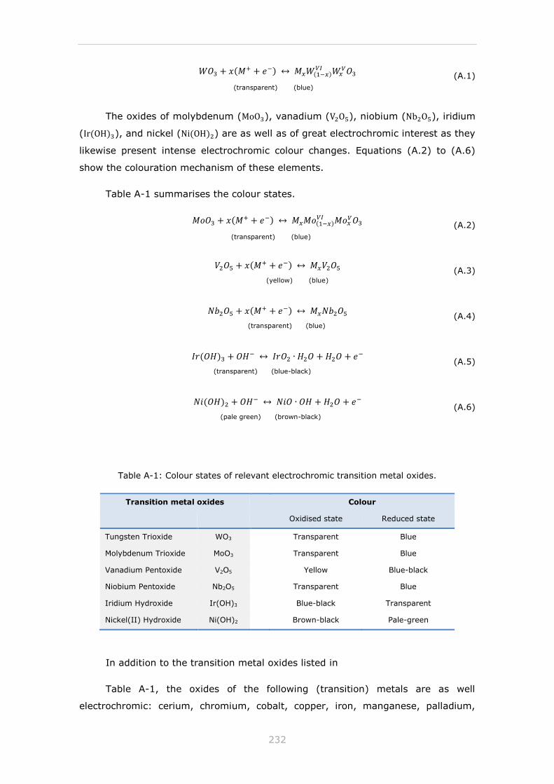
232
𝑊𝑂3 + 𝑥(𝑀+ + 𝑒−) ↔ 𝑀𝑥𝑊(1−𝑥)𝑉𝐼 𝑊𝑥
𝑉𝑂3
(transparent) (blue)
(A.1)
The oxides of molybdenum (MoO3), vanadium (V2O5), niobium (Nb2O5), iridium
(Ir(OH)3), and nickel (Ni(OH)2) are as well as of great electrochromic interest as they
likewise present intense electrochromic colour changes. Equations (A.2) to (A.6)
show the colouration mechanism of these elements.
Table A-1 summarises the colour states.
𝑀𝑜𝑂3 + 𝑥(𝑀+ + 𝑒−) ↔ 𝑀𝑥𝑀𝑜(1−𝑥)𝑉𝐼 𝑀𝑜𝑥
𝑉𝑂3
(transparent) (blue)
(A.2)
𝑉2𝑂5 + 𝑥(𝑀+ + 𝑒−) ↔ 𝑀𝑥𝑉2𝑂5
(yellow) (blue)
(A.3)
𝑁𝑏2𝑂5 + 𝑥(𝑀+ + 𝑒−) ↔ 𝑀𝑥𝑁𝑏2𝑂5
(transparent) (blue)
(A.4)
𝐼𝑟(𝑂𝐻)3 + 𝑂𝐻− ↔ 𝐼𝑟𝑂2 ∙ 𝐻2𝑂 + 𝐻2𝑂 + 𝑒−
(transparent) (blue-black)
(A.5)
𝑁𝑖(𝑂𝐻)2 + 𝑂𝐻− ↔ 𝑁𝑖𝑂 ∙ 𝑂𝐻 + 𝐻2𝑂 + 𝑒−
(pale green) (brown-black)
(A.6)
Table A-1: Colour states of relevant electrochromic transition metal oxides.
Transition metal oxides Colour
Oxidised state Reduced state
Tungsten Trioxide WO3 Transparent Blue
Molybdenum Trioxide MoO3 Transparent Blue
Vanadium Pentoxide V2O5 Yellow Blue-black
Niobium Pentoxide Nb2O5 Transparent Blue
Iridium Hydroxide Ir(OH)3 Blue-black Transparent
Nickel(II) Hydroxide Ni(OH)2 Brown-black Pale-green
In addition to the transition metal oxides listed in
Table A-1, the oxides of the following (transition) metals are as well
electrochromic: cerium, chromium, cobalt, copper, iron, manganese, palladium,
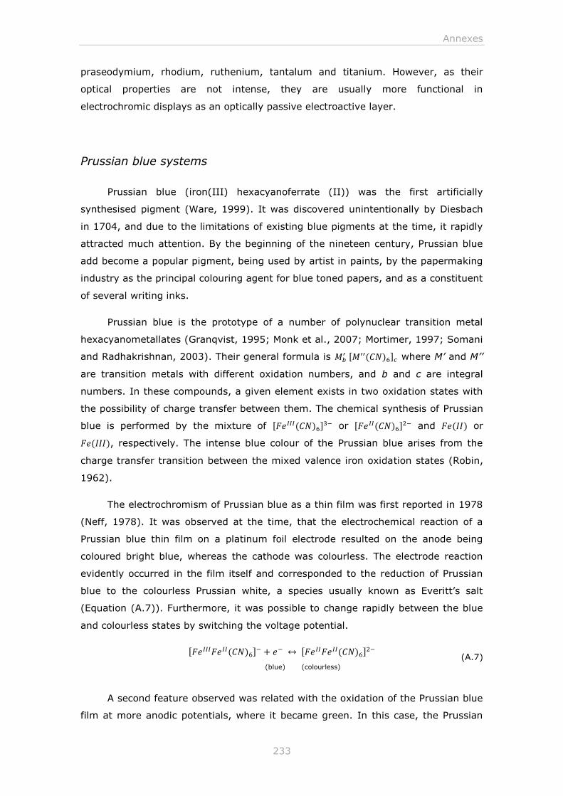
Annexes
233
praseodymium, rhodium, ruthenium, tantalum and titanium. However, as their
optical properties are not intense, they are usually more functional in
electrochromic displays as an optically passive electroactive layer.
Prussian blue systems
Prussian blue (iron(III) hexacyanoferrate (II)) was the first artificially
synthesised pigment (Ware, 1999). It was discovered unintentionally by Diesbach
in 1704, and due to the limitations of existing blue pigments at the time, it rapidly
attracted much attention. By the beginning of the nineteen century, Prussian blue
add become a popular pigment, being used by artist in paints, by the papermaking
industry as the principal colouring agent for blue toned papers, and as a constituent
of several writing inks.
Prussian blue is the prototype of a number of polynuclear transition metal
hexacyanometallates (Granqvist, 1995; Monk et al., 2007; Mortimer, 1997; Somani
and Radhakrishnan, 2003). Their general formula is 𝑀𝑏′ [𝑀′′(𝐶𝑁)6]𝑐 where M’ and M’’
are transition metals with different oxidation numbers, and b and c are integral
numbers. In these compounds, a given element exists in two oxidation states with
the possibility of charge transfer between them. The chemical synthesis of Prussian
blue is performed by the mixture of [𝐹𝑒𝐼𝐼𝐼(𝐶𝑁)6]3− or [𝐹𝑒𝐼𝐼(𝐶𝑁)6]2− and 𝐹𝑒(𝐼𝐼) or
𝐹𝑒(𝐼𝐼𝐼), respectively. The intense blue colour of the Prussian blue arises from the
charge transfer transition between the mixed valence iron oxidation states (Robin,
1962).
The electrochromism of Prussian blue as a thin film was first reported in 1978
(Neff, 1978). It was observed at the time, that the electrochemical reaction of a
Prussian blue thin film on a platinum foil electrode resulted on the anode being
coloured bright blue, whereas the cathode was colourless. The electrode reaction
evidently occurred in the film itself and corresponded to the reduction of Prussian
blue to the colourless Prussian white, a species usually known as Everitt’s salt
(Equation (A.7)). Furthermore, it was possible to change rapidly between the blue
and colourless states by switching the voltage potential.
[𝐹𝑒𝐼𝐼𝐼𝐹𝑒𝐼𝐼(𝐶𝑁)6]− + 𝑒− ↔ [𝐹𝑒𝐼𝐼𝐹𝑒𝐼𝐼(𝐶𝑁)6]2−
(blue) (colourless)
(A.7)
A second feature observed was related with the oxidation of the Prussian blue
film at more anodic potentials, where it became green. In this case, the Prussian
234
blue was oxidised to Prussian green, also known as Berlin green (Equation (A.8)).
Again, the colour could be switched rapidly between blue and green.
3[𝐹𝑒𝐼𝐼𝐼𝐹𝑒𝐼𝐼(𝐶𝑁)6]− ↔ 𝐹𝑒3𝐼𝐼𝐼[𝐹𝑒𝐼𝐼𝐼(𝐶𝑁)6]2[𝐹𝑒𝐼𝐼(𝐶𝑁)6]− + 2𝑒−
(blue) (green)
(A.8)
However, the transition of Prussian blue to Prussian green corresponded only
to the partial electrochemical oxidation of the Prussian blue chromophore, as the
complete oxidation results in a golden yellow Prussian yellow (Equation (A.9)).
[𝐹𝑒𝐼𝐼𝐼𝐹𝑒𝐼𝐼(𝐶𝑁)6]− ↔ [𝐹𝑒𝐼𝐼𝐼𝐹𝑒𝐼𝐼𝐼(𝐶𝑁)6] + 𝑒−
(blue) (yellow)
(A.9)
The electrochemical oxidation of Prussian blue hence presents a continuous
mixed-valence composition between the yellow and blue states by the adjustment
of the potential. By contrast, the reduction of Prussian blue to Prussian white is
abrupt, involving the clean conversion of one element into the other at a critical
potential (Mortimer and Rosseinsky, 1984). The spectra of the different forms of
Prussian blue are shown in Figure A-1.
(a): +0.50V (blue )
(b): −0.20V (colourless)
(c): +0.80V (green)
(d): +0.85V (green)
(e): +0.90V (green)
(f): +1.20V (yellow)
Figure A-1: Spectra of iron hexacyanoferrate films on tin-doped indium oxide (ITO)/glass at
various voltage potentials. Source: (Mortimer, 2011).
The first electrochromic display to use Prussian blue as electrochromic
material was reported by Itaya et al. (Itaya et al., 1982). The seven-segment
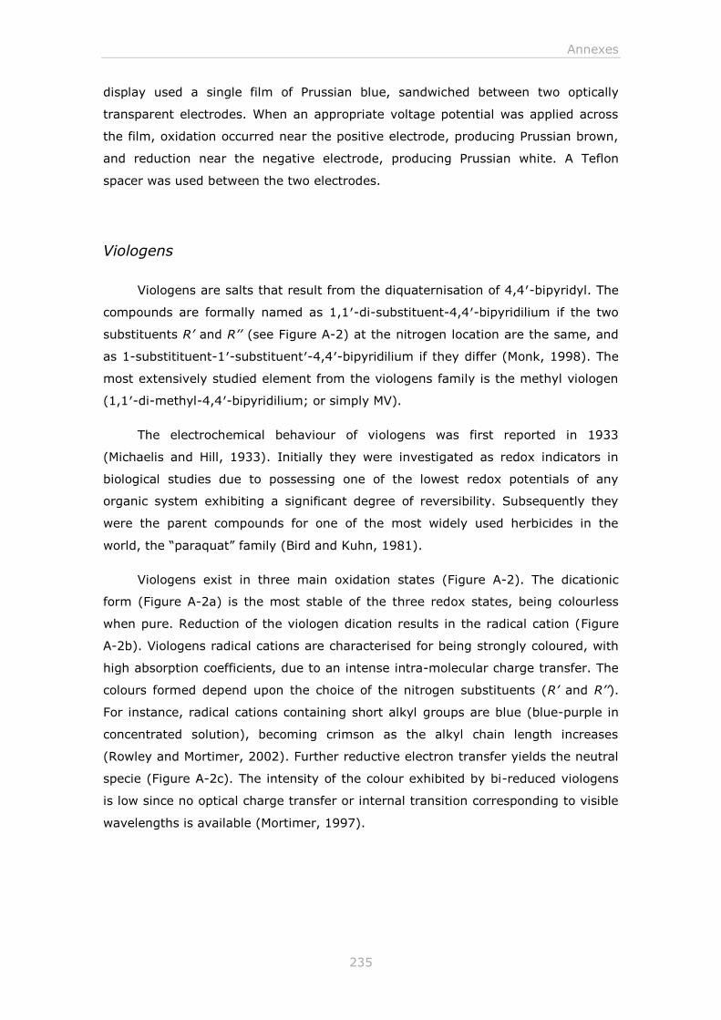
Annexes
235
display used a single film of Prussian blue, sandwiched between two optically
transparent electrodes. When an appropriate voltage potential was applied across
the film, oxidation occurred near the positive electrode, producing Prussian brown,
and reduction near the negative electrode, producing Prussian white. A Teflon
spacer was used between the two electrodes.
Viologens
Viologens are salts that result from the diquaternisation of 4,4′-bipyridyl. The
compounds are formally named as 1,1′-di-substituent-4,4′-bipyridilium if the two
substituents R’ and R’’ (see Figure A-2) at the nitrogen location are the same, and
as 1-substitituent-1′-substituent′-4,4′-bipyridilium if they differ (Monk, 1998). The
most extensively studied element from the viologens family is the methyl viologen
(1,1′-di-methyl-4,4′-bipyridilium; or simply MV).
The electrochemical behaviour of viologens was first reported in 1933
(Michaelis and Hill, 1933). Initially they were investigated as redox indicators in
biological studies due to possessing one of the lowest redox potentials of any
organic system exhibiting a significant degree of reversibility. Subsequently they
were the parent compounds for one of the most widely used herbicides in the
world, the “paraquat” family (Bird and Kuhn, 1981).
Viologens exist in three main oxidation states (Figure A-2). The dicationic
form (Figure A-2a) is the most stable of the three redox states, being colourless
when pure. Reduction of the viologen dication results in the radical cation (Figure
A-2b). Viologens radical cations are characterised for being strongly coloured, with
high absorption coefficients, due to an intense intra-molecular charge transfer. The
colours formed depend upon the choice of the nitrogen substituents (R’ and R’’).
For instance, radical cations containing short alkyl groups are blue (blue-purple in
concentrated solution), becoming crimson as the alkyl chain length increases
(Rowley and Mortimer, 2002). Further reductive electron transfer yields the neutral
specie (Figure A-2c). The intensity of the colour exhibited by bi-reduced viologens
is low since no optical charge transfer or internal transition corresponding to visible
wavelengths is available (Mortimer, 1997).
236
Figure A-2: The three common redox states of Viologens: a) dication, b) radical cation, and
c) neutral species. Source: adapted from (Mortimer et al., 2006).
The first reduction step is highly reversible and can be cycled several times
without significant side reaction. In contrast, the reduction to the fully reduced
state (the neutral species) is less reversible, not only because the latter is
frequently an insoluble species but also because is an uncharged one (Bird and
Kuhn, 1981). Viologens can also be incorporated into polymers, the resulting
materials retaining to a great extent the chemical and electrochemical properties of
the viologen species.
The first application of viologens as electrochromic material in electrochromic
displays was reported in 1973, by Schoot et al. (Schoot et al., 1973).
Conjugated conducting polymers
Conjugated conducting polymers (see for instance, (Chandrasekhar, 1999;
Chilton and Goosey, 1995; Inzelt, 2012)) are organic polymers that exhibit high
electrical conductivity. They are produced by either chemical or electrochemical
polymerization of various aromatic molecules, such as pyrrole, thiophene, aniline,
furan, carbazole, azulene or indole (Figure A-3).
The conductivity of the conjugated polymer is achieved through the process of
“doping”. This essentially consists of the oxidation (p-doping), or in some cases
reduction (n-doping), of the polymeric backbone by a number of simple anionic or
cationic species (dopants) with the aim of creating charge carriers. Conjugated
polymers possess a unique, extended -conjugation structure, alternating simple
a) b) c)
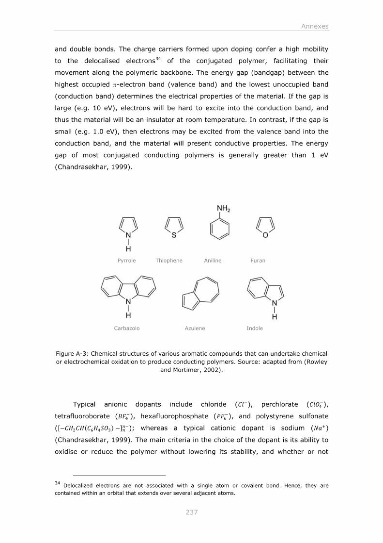
Annexes
237
and double bonds. The charge carriers formed upon doping confer a high mobility
to the delocalised electrons34 of the conjugated polymer, facilitating their
movement along the polymeric backbone. The energy gap (bandgap) between the
highest occupied -electron band (valence band) and the lowest unoccupied band
(conduction band) determines the electrical properties of the material. If the gap is
large (e.g. 10 eV), electrons will be hard to excite into the conduction band, and
thus the material will be an insulator at room temperature. In contrast, if the gap is
small (e.g. 1.0 eV), then electrons may be excited from the valence band into the
conduction band, and the material will present conductive properties. The energy
gap of most conjugated conducting polymers is generally greater than 1 eV
(Chandrasekhar, 1999).
Figure A-3: Chemical structures of various aromatic compounds that can undertake chemical
or electrochemical oxidation to produce conducting polymers. Source: adapted from (Rowley
and Mortimer, 2002).
Typical anionic dopants include chloride (𝐶𝑙−), perchlorate (𝐶𝑙𝑂4−),
tetrafluoroborate (𝐵𝐹4−), hexafluorophosphate (𝑃𝐹6
−), and polystyrene sulfonate
([−𝐶𝐻2𝐶𝐻(𝐶6𝐻4𝑆𝑂3) −]𝑛𝑛−); whereas a typical cationic dopant is sodium (𝑁𝑎+)
(Chandrasekhar, 1999). The main criteria in the choice of the dopant is its ability to
oxidise or reduce the polymer without lowering its stability, and whether or not
34
Delocalized electrons are not associated with a single atom or covalent bond. Hence, they are
contained within an orbital that extends over several adjacent atoms.
Pyrrole Thiophene Aniline Furan
Carbazolo Azulene Indole
238
they are capable of initiating side reactions that inhibit the polymers capability to
conduct electricity.
The first chemical oxidative polymerization dates back to 1892 when Letheby
(Letheby, 1862), while investigating two cases of fatal poisoning by nitrobenzol,
and finding that this compound changed in the living stomach into aniline, decided
to study into the chemical reactions of aniline. He observed that the electrolytic
oxidation of a sulphatic solution of aniline resulted in a blue pigment (polyaniline),
when the reduced form was colourless. However, the modern study of electric
conduction in conjugated polymers only began in 1977 (see (Scott, 2010) for a
thorough description), when Chian et al. reported the doping of polyacetylene
(Chiang et al., 1977). Following this publication, numerous research groups began
programs to understand better the properties of conjugated conducting polymers,
and to search for new and better materials. Research papers on the topic became
systematic. In less than a decade, most of the monomer building blocks that we
know today had been identified and many procedures for polymeric synthesis had
been documented. In 2000, the Nobel Committee recognised the crucial
contributions of Heeger (Heeger, 2001), MacDiarmid (MacDiarmid, 2001) and
Shirakawa (Shirakawa, 2001) in "[...] the discovery and development of conductive
polymers" (Nobel Media AB, n.d.), awarding them the Nobel Prize in Chemistry.
All conjugated conducting polymers are potentially electrochromic in thin film
form. They exhibit different colours whether they are in the oxidised (doped) or
reduced (undoped) form. The colour change or contrast between the doped and
undoped forms depends on the magnitude of the energy gap (bandgap) of the
undoped form. Thin films with an energy gap greater than 3 eV (~400 nm) are
colourless and transparent in the undoped form, while in the doped form their
absorption spectrum is generally in the visible region. In turn, those with an energy
gap equal to or less than 1.5 eV (~800 nm) are highly absorbing in the visible
spectrum when in the undoped form but, after doping, the absorption in the visible
spectrum is weak, being transferred to the near infrared. The polymers with the
intermediate energy gaps are the ones more that present the most distinct optical
changes throughout the visible spectrum (Mortimer et al., 2006).
Furthermore, conjugated conducting polymers can be tailored to induce other
colour changes, i.e. they can be designed for a particular energy gap. This can be
achieved by changing the composition of the polymers at the molecular level using
a variety of synthetic strategies (see (Beaujuge and Reynolds, 2010; Stenger-
Smith, 1998)) such as, varying the overall planarity of the polymer backbone, or by
copolymerizing different monomers. The blending of different electroactive
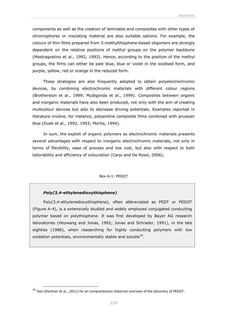
Annexes
239
components as well as the creation of laminates and composites with other types of
chromophores or insulating material are also suitable options. For example, the
colours of thin films prepared from 3-methylthiophene-based oligomers are strongly
dependent on the relative positions of methyl groups on the polymer backbone
(Mastragostino et al., 1992, 1993). Hence, according to the position of the methyl
groups, the films can either be pale blue, blue or violet in the oxidised form, and
purple, yellow, red or orange in the reduced form.
These strategies are also frequently adopted to obtain polyelectrochromic
devices, by combining electrochromic materials with different colour regions
(Brotherston et al., 1999; Mudigonda et al., 1999). Composites between organic
and inorganic materials have also been produced, not only with the aim of creating
multicolour devices but also to decrease driving potentials. Examples reported in
literature involve, for instance, polyaniline composite films combined with prussian
blue (Duek et al., 1992, 1993; Morita, 1994).
In sum, the exploit of organic polymers as electrochromic materials presents
several advantages with respect to inorganic electrochromic materials, not only in
terms of flexibility, ease of process and low cost, but also with respect to both
tailorability and efficiency of colouration (Carpi and De Rossi, 2006).
Box A-1: PEDOT
Poly(3,4-ethylenedioxythiophene)
Poly(3,4-ethylenedioxythiophene), often abbreviated as PEDT or PEDOT
(Figure A-4), is a extensively studied and widely employed conjugated conducting
polymer based on polythiophene. It was first developed by Bayer AG research
laboratories (Heywang and Jonas, 1992; Jonas and Schrader, 1991), in the late
eighties (1988), when researching for highly conducting polymers with low
oxidation potentials, environmentally stable and soluble35.
35 See (Elschner et al., 2011) for an comprehensive historical overview of the discovery of PEDOT.
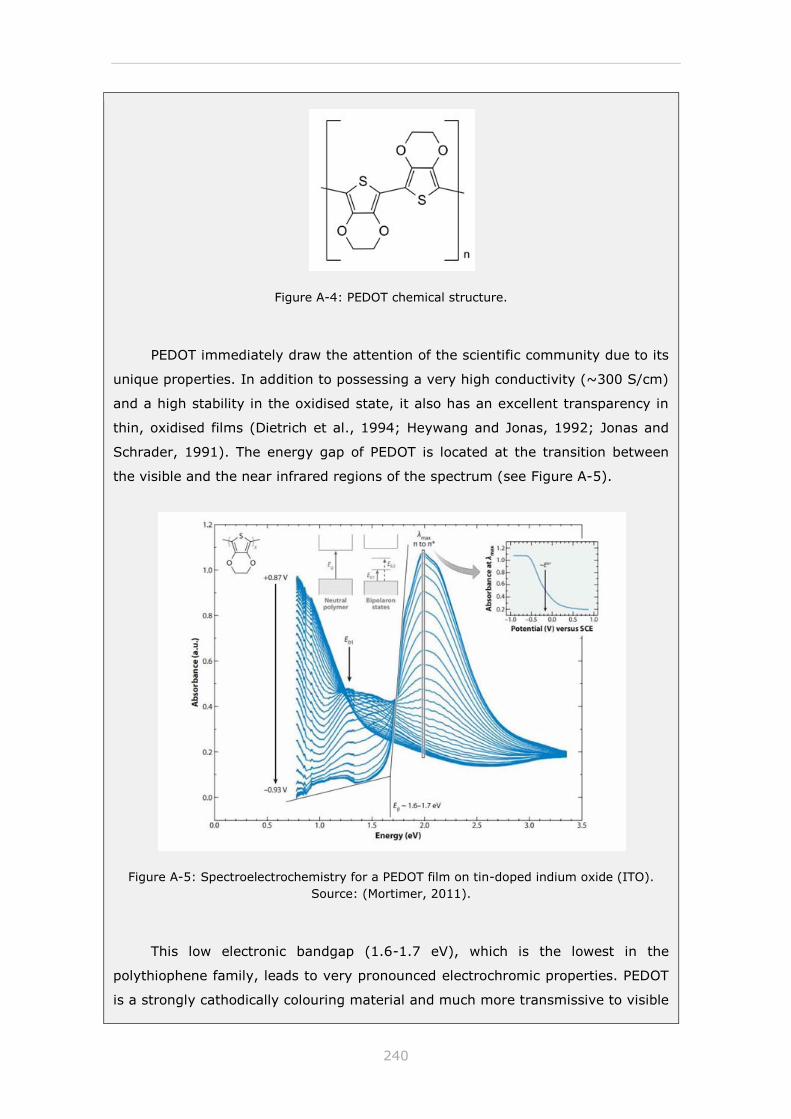
240
Figure A-4: PEDOT chemical structure.
PEDOT immediately draw the attention of the scientific community due to its
unique properties. In addition to possessing a very high conductivity (~300 S/cm)
and a high stability in the oxidised state, it also has an excellent transparency in
thin, oxidised films (Dietrich et al., 1994; Heywang and Jonas, 1992; Jonas and
Schrader, 1991). The energy gap of PEDOT is located at the transition between
the visible and the near infrared regions of the spectrum (see Figure A-5).
Figure A-5: Spectroelectrochemistry for a PEDOT film on tin-doped indium oxide (ITO).
Source: (Mortimer, 2011).
This low electronic bandgap (1.6-1.7 eV), which is the lowest in the
polythiophene family, leads to very pronounced electrochromic properties. PEDOT
is a strongly cathodically colouring material and much more transmissive to visible
Annexes
241
light in the doped and conducting state than it is in the reduced state (Pei et al.,
1994). In this state, PEDOT exhibits a highly absorbing deep-blue colour while is
almost transparent in the oxidise form, exhibiting a light-blue colour.
Unfortunately, like most conducting polymers, PEDOT is insoluble and therefore
difficult to process in thin film form. The solubility problem was eventually
overcome by Bayer through the use of a water soluble polyelectrolyte,
poly(styrene sulfonate) (commonly known as PSS), as the charge balancing
dopant during the polymerization of PEDOT to yield PEDOT:PSS (Figure A-6). The
result was a water soluble polyelectrolyte system with good film forming
properties, high conductivity36, high visible light transmissivity, and excellent
stability (Groenendaal et al., 2000; Jonas et al., 1995). The lower price of
PEDOT:PSS when compared to other alternatives also makes it a commercially
attractive material.
Figure A-6: Chemical structure of PEDOT:PSS. Source: adapted from (Monk et al., 2007).
The electrochromic colouration mechanism of PEDOT:PSS is show in
Equation (A.10), where M+ represents one of the following cations: H+, Li+, Na+,
or K+; and e- designates the electrons.
𝑃𝐸𝐷𝑂𝑇+𝑃𝑆𝑆− + 𝑀+ + 𝑒− ↔ 𝑃𝐸𝐷𝑂𝑇0+𝑃𝑆𝑆−𝑀+
(transparent light-blue) (deep blue)
(A.10)
The physical properties of PEDOT:PSS make it possible for it to be selectively
deposit, with a relative ease, into an assortment of substrates, whether they be
rigid (e.g. glass) or flexible (e.g. paper). This is usually achieved by applying it as
36 As an example, the commercially available solution produced by Heraeus with the trade name Clevios
can have a conductivity of up to 1000 S/cm (Heraeus Precious Metals, 2012).
242
a water dispersion using standard coating or printing processes. Screen printing
(see for instance, (McGarry and Tarr, 2008)), line patterning (see (Hohnholz et
al., 2005)), and ink-jet printing (see (Tekin et al., 2008)) are the most commonly
used manufacturing techniques. These methods not only reduce the number of
fabrication steps but also eliminate the need for high-vacuum processing (Sankir,
2008).
The first description of a PEDOT based electrochromic device was reported
by Gustafsson-Carlberg et al., in 1995 (Gustafsson-Carlberg et al., 1995). The
device was assembled when the authors were investigating the use of PEDOT and
other conducting polymers of the polythiophene family in electrochromic
applications (smart windows and displays). It consisted of a solid state
electrochromic cell formed by one PEDOT layer on a tin-doped indium oxide
(indium tin oxide, or simply ITO) coated glass electrode, and one vanadium oxide
layer, also on an ITO coated glass electrode, separated by a solid polymer
electrolyte. The use of PEDOT as the electrochromic material in solid state
electrochemical cells demonstrated that it was possible to construct
electrochromic devices with relatively small switching voltages (~1.5 V). In 2003,
Argun et al. (Argun et al., 2003) reported the first truly all-polymer electrochromic
device based on PEDOT:PSS. However, in this case, PEDOT:PSS was not used as
the electrochromic layer but instead as the transparent electrode material,
replacing the traditionally used ITO electrodes. As the electrochromic layer was
used another cathodically colouring electrochromic polymer, and since the
electroactive layer was also formed by an electrochromic polymer, the device was
constructed using only organic and polymeric components. More recently,
Andersson and co-workers (Andersson et al., 2007) combined an PEDOT:PSS
based electrochemical transistor with an PEDOT:PSS based electrochromic display
cell to form electrochemical smart pixels and build an all-organic active matrix
addressed paper display (see also section 4.1.2.1.3). Here, PEDOT:PSS served
both as the active material in the electrochemical smart pixels, as well as the
conducting lines to route the updating signals of the integrated active-matrix
display.
Metallopolymers
Metallopolymers (see for instance, (Maclanchlan, 2007; Wild et al., 2011)) are
conjugated polymers that contain transition metal complexes. The great interest in
these materials is related to their unique properties, which represent a combination
Annexes
243
of the physical, electronic and optical properties of the organic polymer with the
physical, electronic and optical properties of the incorporated metal complex.
Depending on the arrangement of the metal group relatively to the polymer
backbone, metallopolymers can be divided into three types (Figure A-7) (Wolf,
2001):
- Type I metallopolymers have the metal group bind to the conjugated
polymer backbone by a linker such as an alkyl group. The large connection
distance between the polymer and the complexes results in no, or only
weak, interaction between both. The polymer acts primarily as a
conductive support and the electronic, optical, and chemical properties of
the metal group are essentially the same as those of the unbind complex.
- In Type II metallopolymers, the metal is directly coupled to the conjugated
polymer backbone making it easier for the polymer and metal group to
affect each other's properties. Since -conjugated backbones and many
metal groups are redox active, the system might be able to be
electrochemically tuned.
- Last, type III metallopolymers have the metal group directly incorporated
into the conjugated polymer backbone. In this type of arrangement, strong
electronic interactions between the organic bridge and metal group are
possible. The properties of the conducting polymer are greatly influenced
by the metal.
Figure A-7: Schematic representation of the three different types of structures of
metallopolymers. Source: adapted from (Wolf, 2001).
244
The synthesis of metallopolymers can be done using a variety of methods
(Wild et al., 2011). The most commonly used include condensation (Kingsborough
and Swager, 2007), ring-opening metathesis (Buretea and Tilley, 1997) and
electropolymerisation (Wolf, 2001). The successful free radical polymerization of
vinyl ferrocene, reported in 1955, marks the first metal-containing polymer,
poly(vinylferrocene) (Arimoto and Haven, 1955).
The use of metallopolymers as functional materials has been under
investigation for the last decades, and a variety of potential applications are
proposed (Holliday and Swager, 2005; Whittell and Manners, 2007; Whittell et al.,
2011; Williams et al., 2007; Wolf, 2001). These include the use of metallopolymers
as photoelectronic and electroluminescent devices; as photovoltaic materials; as
electro-responsive sensors; as data storage devices; as molecular wires, switches,
and antennae; and as macromolecular catalysts and artificial enzymes.
In terms of electrochromism, metallopolymers are attractive because of their
intense colouration and ample redox reactivity. The chromophoric properties of
metallopolymers usually emerge either from low-energy metal-to-ligand charge
transfer (MLCT), intervalence charge transfer (IVCT), intraligand excitation, or
related visible-region electronic transitions. Since all these transitions involve
valence electrons, the chromophoric characteristics of the complex are altered or
eliminated once it is oxidise or reduced (Monk et al., 2007; Zhang et al., 1992).
Multicolour electrochromic changes can be induced by introducing two distinct types
of metal ions into the polymer structure (see, (Higuchi, 2009; Higuchi et al.,
2008)).
Good examples of metal coordination complexes with the potential for use in
electrochromic devices include the [𝑀𝐼𝐼(𝑏𝑖𝑝𝑦)3]2+ series (Mortimer, 2011), where 𝑀𝐼𝐼
corresponds to one of the following metal elements: iron (𝐹𝑒), ruthenium (𝑅𝑢), or
osmium (𝑂𝑠); and 𝑏𝑖𝑝𝑦 to 2,2’-bipyridine. The choice of one metal complex over the
other influences the colour of the metallopolymer film in the 𝑀𝐼𝐼 redox state. Using
iron as the metal complex confers a red colour to the thin film; while ruthenium
gives it an orange colouration. In turn, osmium confers a green colour to the thin
film. As an example, Zeng et al. (Zeng et al., 2008) reported on a Ru-phenolate
based metallopolymer (metallopolymer incorporating a ruthenium metal centre)
capable exhibiting rich electrochromic behaviour in the visible and near infrared
regions of the electromagnetic spectrum, whereas in solution or in thin film form.
The oxidation at 0.5 eV resulted in a change of colour from wine red to light green
while potentials above 1.5 eV produced a change in the near infrared region.
Annexes
245
Annex B - Types of Electrolytes
Electrolytes function as a source and sink of cations and anions as the various
redox processes take place in an electrochromic displays. In the following sub-
sections is briefly described the different classes of electrolytes commonly used in
electrochromic displays.
Liquid electrolytes
Liquid electrolytes are characterised for having high ionic conductivities. The
ionic transport is realised in a two-step process. First, the solvation and dissociation
of the ionic compounds by the solvent molecules occurs, and second, the solvated
ions migrate through the solvent medium. The excellent conductivity results from
the combination of the ionic mobility and dissociation constant of the electrolyte
system (Xu, 2004).
Solvent composition tailoring has been the main tool for manipulating
electrolyte ion conductivity due to the availability of a vast number of candidate
solvents (Xu, 2004). Since the advent of non-aqueous electrolytes, a wide
spectrum of polar solvents has been investigated. The majority of them fall into
either one of the following families: organic esters and ethers. Among these
solvents, cyclic diesters of carbonic acid have undoubtedly attracted the main
research attention. The most commonly used are propylene carbonate (PC),
ethylene carbonate (EC) and -butyrolactone (-BL).
Ideally, liquid electrolyte solvents should: (1) be able to dissolve salts to a
sufficient concentration; (2) have a low viscosity, so that facile ion transport can
occur; (3) remain inert to all components of the electrochemical cell, especially the
charged surfaces of the cathode and the anode; (4) remain liquid in a wide
temperature range, i.e. its melting point should be low and its boiling point high;
(5) be nontoxic; and (6) be economical (Xu, 2004).
246
Early electrochromic devices used liquid electrolytes as medium by excellence.
For example, Deb’s (Deb, 1969) novel electrochromic device used an aqueous
solution of sulphuric acid (𝐻2𝑆𝑂4) as electrolyte. Liquid acids are now rarely
employed because of their tendency to degrade or dissolve electrochromic materials
and because of fears that the device will leak (Mortimer, 1997). Another popular
electrolyte solute was Lithium perchlorate (𝐿𝑖𝐶𝑙𝑂4). However, the high oxidation
state of chlorine (VII) in perchlorate makes it a strong oxidant, which readily reacts
with most organic species in violent ways under certain conditions such as high
temperature and high current charge (Jasinski and Carroll, 1970).
The main drawbacks in using liquid electrolytes are related to problems of
leakage of the electrolyte solution, the weight gain from the solution, the low
chemical stability, and homogeneity problems during the colouration process. A
thickener, such as an acrylic polymer, poly(vinylbutyral), or colloidal silica, can be
added to the liquid electrolyte solution to increase its viscosity and improve the
safety of a electrochromic device should rupture occurs. Moreover, it helps
minimize the effects of mass transport by natural convection. Clearly, as the
addition of the polymer thickener is continued, the viscosity increases to the point
where eventually the solution is self-supporting or free standing, and can be
considered a physical gel (Byker, 2001).
Gel electrolytes
Gel electrolytes have a unique hybrid structure that consists of a polymer
matrix swollen in a liquid medium (solvent). The liquid medium prevents the
polymer matrix from collapsing into a compact mass whereas the polymer matrix,
in turn, provides the microstructure to retain the liquid medium. The particularity of
this arrangement is that the liquid medium, i.e. the solvent, is dissolved in the
polymer matrix and not the other way around. The interactions between the
polymer matrix and the liquid medium result in the electrolyte possessing
simultaneously the cohesive properties of solid electrolytes and the diffusive
transport properties of liquids electrolytes (Byker, 2001; Song et al., 1999).
Gel electrolytes are usually prepared by incorporating large quantities of a
liquid plasticiser, alongside with the solvent(s), into the polymer matrix. The aim of
the liquid plasticiser is to adjust the viscosity and improve the performance, namely
the ionic conductivity, of the electrolyte. The excessive addition of the liquid
plasticiser leads to the gel electrolyte presenting the same problems commonly
Annexes
247
associated to liquid electrolytes, as pointed out in the previous sub-section. Typical
solvent plasticisers used are ethylene carbonate, propylene carbonate, dimethyl
sulphoxide, dimethyl carbonate and diethyl carbonate.
Gel electrolytes are obtained as a result of either a chemical or a physical
cross-linking process (Song et al., 1999). The chemical cross-link occurs when
covalent bonds are created between the polymer chains by means of a chemical
reaction to form a certain number of tie or junction points. In this case, as the
number of junction points basically does not change upon the variation of the
external conditions such as temperature, concentration, or stress, it leads to the
formation of irreversible gels. Physical cross-link, on the contrary, occurs when the
polymeric chains interact over a portion of their length or align in some regions to
form small crystallites. In this case, “van der Waals” forces are responsible for
joining the polymer chains and the solvent. Due to their weak nature, the
connections can be broken by external conditions. The cross-linked polymer is
typically formed by in-situ polymerization once the electrochromic device is filled
with the solution containing the necessary polymer forming materials. Most gel
electrolytes are based on polymer matrixes of polyacrylonitrile (PAN), poly(ethylene
oxide) (PEO), poly(methyl methacrylate) (PMMA), poly(vinylchloride) (PVC),
poly(vinyl pyrrolidone) (PVP), and poly(vinylidene fluoride) (PVDF).
The salts dissolved in the solution phase of a chemical or physical gel have
ionic conductivities approaching those of liquid electrolytes. For example, gel
electrolytes based on poly(methylmethacrylate) (PMMA) have room temperature
conductivities of 10-3 S/cm (Agnihotry et al., 2000).
Solid electrolytes
Solid electrolytes generally have lower ionic conductivities than gel and liquid
electrolytes. These lower conductivities arise from the slower ion diffusion through
the solvated polymer matrix as a consequence of the higher viscosities. However,
as electrochromic devices do not require high conductivity values due to the close
proximity of the electrodes in the assembled electrochromic device, solid
electrolytes that present ionic conductivities in the order of 10−4 S/cm at room
temperature are adequate for use (Przyluski et al., 1993).
Solid electrolytes are obtained through the dissolution of salts in ion-
coordinating macromolecules (the polymer matrix) liberated of any low weight
solvent or additives (Bruce and Vincent, 1993). A wide variety of salts based on
248
alkali-metal, alkaline-earth-metal, transition-metal and lanthanide ions can be
used. The classic polymer host used is poly(ethylene oxide) (PEO) because of its
solvation power and complexing ability to alkali metal ion (Liang and Kuo, 2004).
Other commonly used polymer matrixes are polyacrylonitrile (PAN), poly(methyl
methacrylate) (PMMA), poly(vinylchloride) (PVC), poly(vinyl pyrrolidone) (PVP), and
poly(vinylidene fluoride) (PVDF), as already seen in gel electrolytes.
Solid electrolytes are typically formed by one of two methods. Thin films can
either be fabricated by using solvent evaporation coating techniques, namely
solvent casting, where basically the solvent is slowly removed from a homogeneous
solution of polymer and salt; or, alternatively, by cryogenic grinding appropriate
mixtures of polymer and salt and then subject the resulting powder to a modest
heat treatment (Bruce and Vincent, 1993).
The advantage of using solid electrolytes in electrochromic devices is related
to their mechanical and chemical stability. Furthermore, solid electrolytes have an
excellent adhesive behaviour forming good interfacial contacts with the electrodes,
and excellent elastomeric characteristics, being capable to relax elastically when
under stress. In sum, they eliminate the problems associated with electrolyte
evaporation and leakage, increase of hydrostatic pressure and device deformation,
and undesired oxidation-reduction reactions with the electroactive materials. The
need for a hermetic sealing is also eliminated.
Hybrid electrolytes
Hybrid electrolytes are organic–inorganic polymer electrolytes. The main
synthetic route for the formation of these innovative systems is the sol–gel method
(see (Brinker and Scherer, 1990)). The process consists of the formation of a gel
system from a colloidal suspension of solid particles in a liquid, the sol. The sol is
typically obtained through the hydrolysis and partial condensation of a precursor
such as an inorganic metal salt or a metal organic compound (usually a metal
alkoxide). The high versatility of the sol-gel method and the wide variety of
precursors offers important advantages for the preparation of hybrid organic–
inorganic electrolytes. It allows the incorporation of various organic polymers and
molecules in the inorganic polymers, and thus the preparation of organic–inorganic
hybrids that exhibit different physical and chemical properties depending on the
organic phase and on the inorganic matrix (Orel et al., 2003). As a result, these
hybrid materials combine the most important properties of their constituents, such
Annexes
249
as high transparency, low processing temperatures, sufficient thermal stability, and
with high-performance yield, properties not found together in either material
individually.
Based on the nature of the inner interfaces verified between the organic and
inorganic phases, organic-inorganic hybrid materials can be divided into two distinct
classes (Judeinstein and Sanchez, 1996): in class I (or type I), organic and
inorganic compounds are held together only by weak bonds, namely hydrogen, van
der Waals or ionic bonds; in class II (or type II), the two phases are linked together
through strong chemical bonds, such as covalent bonds. Hybrid electrolytes should
preferably be of type II. The ionic conductivity of hybrid electrolytes is only
marginally smaller than that of liquid electrolytes.
Ionic liquid electrolytes
Ionic liquids are organic salts with a low melting point (below 100 ºC). They
are, hence, typically liquid at room temperature. The most impressive feature of
ionic liquids is the wide range of possible variations in their properties. In theory,
ionic liquids can be designed to deliver almost any set of physical and chemical
properties for almost any application in the chemical sciences (Freemantle, 2009).
The tailoring of the physical, chemical and biological properties of ionic liquids is
commonly done by changing the nature of the cations or anions; by introducing
specific functionalities directly into the cations or anions, i.e. by changing their
structure; or by mixing two or more simple ionic liquid (see (Freemantle, 2009;
Seddon et al., 2000)). However, in practice, ionic liquids are usually selected for an
application based on their properties rather than being specifically designed for it.
The unique properties that certain ionic liquids present has made them
emerge as promising elements for electrolyte systems in electrochemical devices.
In general, they have a high ionic conductivity (~10-2 S/cm) associated with
excellent chemical and thermal stabilities. Furthermore, they feature low or
negligible volatility, low flammability, and a wide electrochemical potential window.
Two main strategies have been pursued by the scientific community in an attempt
to translate the benefits of ionic liquids to polymer electrolytes. The first strategy
involves the design of electrolyte systems composed of conventional polymer
matrixes and ionic liquids; while the second consists of designing functional
polymers presenting some of the characteristics of ionic liquids (Marcilla et al.,
2006).
250
The implementation of ionic liquid based electrolytes in real electrochromic
devices demonstrated that ionic liquids can indeed radically improve the
performance, speed, cyclability and long term stability of electrochromic devices
(Lu et al., 2002, 2003; Marcilla et al., 2006). The benefits of ionic liquids based
electrolytes in electrochromic displays was first reported by Lu et al. (Lu et al.,
2002).
Examples of ionic liquids suitable to be used in electrolytes for electrochromic
devices are: ethyl ammonium nitrate ([𝐸𝑡𝑁𝐻3][𝑁𝑂3]), 1-butyl-3-methylimidazolium
tetrafluoroborate ([𝐵𝑀𝐼𝑀][𝐵𝐹4]) or 1-butyl-3-methylimidazolium hexafluoro-
phosphate ([𝐵𝑀𝐼𝑀][𝑃𝐹6]).
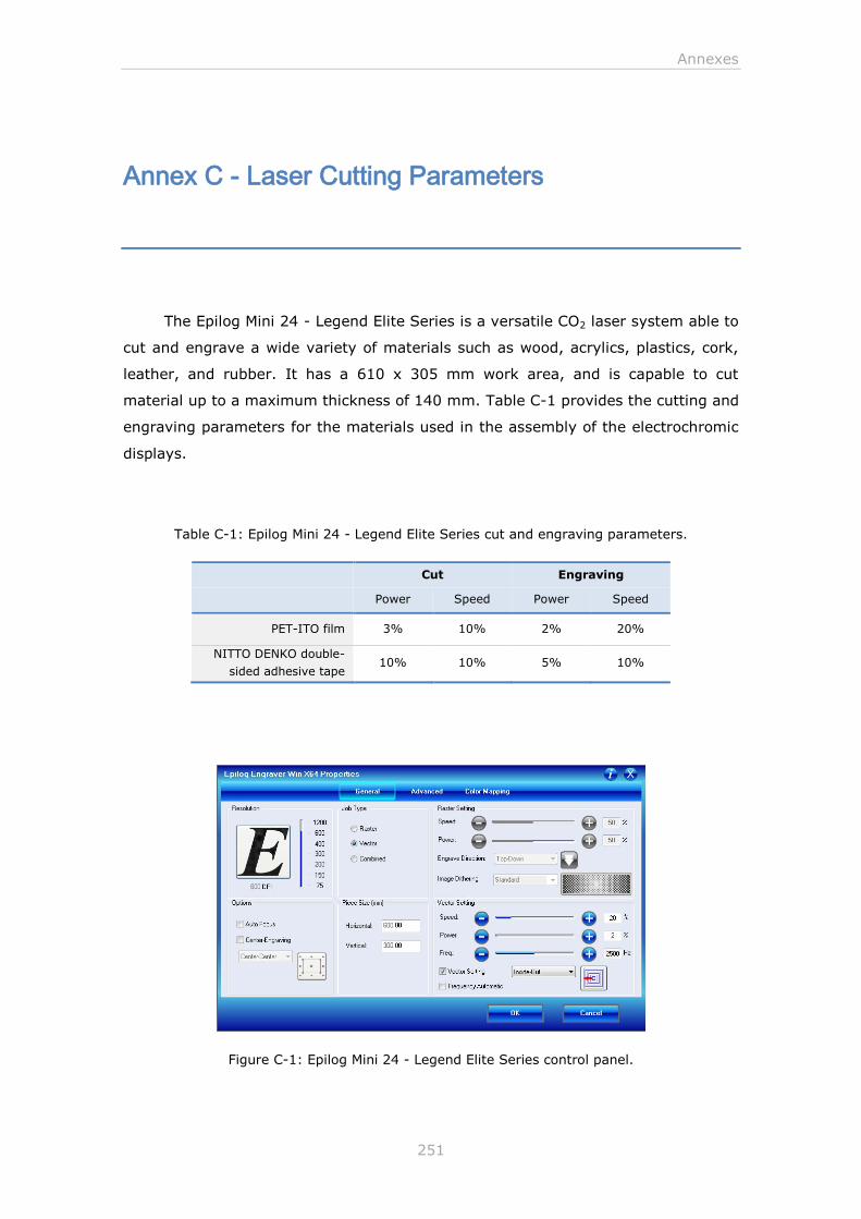
Annexes
251
Annex C - Laser Cutting Parameters
The Epilog Mini 24 - Legend Elite Series is a versatile CO2 laser system able to
cut and engrave a wide variety of materials such as wood, acrylics, plastics, cork,
leather, and rubber. It has a 610 x 305 mm work area, and is capable to cut
material up to a maximum thickness of 140 mm. Table C-1 provides the cutting and
engraving parameters for the materials used in the assembly of the electrochromic
displays.
Table C-1: Epilog Mini 24 - Legend Elite Series cut and engraving parameters.
Cut Engraving
Power Speed Power Speed
PET-ITO film 3% 10% 2% 20%
NITTO DENKO double-
sided adhesive tape 10% 10% 5% 10%
Figure C-1: Epilog Mini 24 - Legend Elite Series control panel.

252
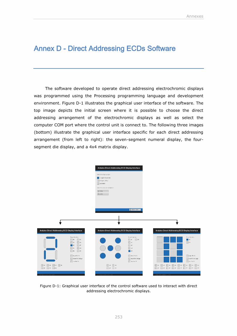
Annexes
253
Annex D - Direct Addressing ECDs Software
The software developed to operate direct addressing electrochromic displays
was programmed using the Processing programming language and development
environment. Figure D-1 illustrates the graphical user interface of the software. The
top image depicts the initial screen where it is possible to choose the direct
addressing arrangement of the electrochromic displays as well as select the
computer COM port where the control unit is connect to. The following three images
(bottom) illustrate the graphical user interface specific for each direct addressing
arrangement (from left to right): the seven-segment numeral display, the four-
segment die display, and a 4x4 matrix display.
Figure D-1: Graphical user interface of the control software used to interact with direct
addressing electrochromic displays.
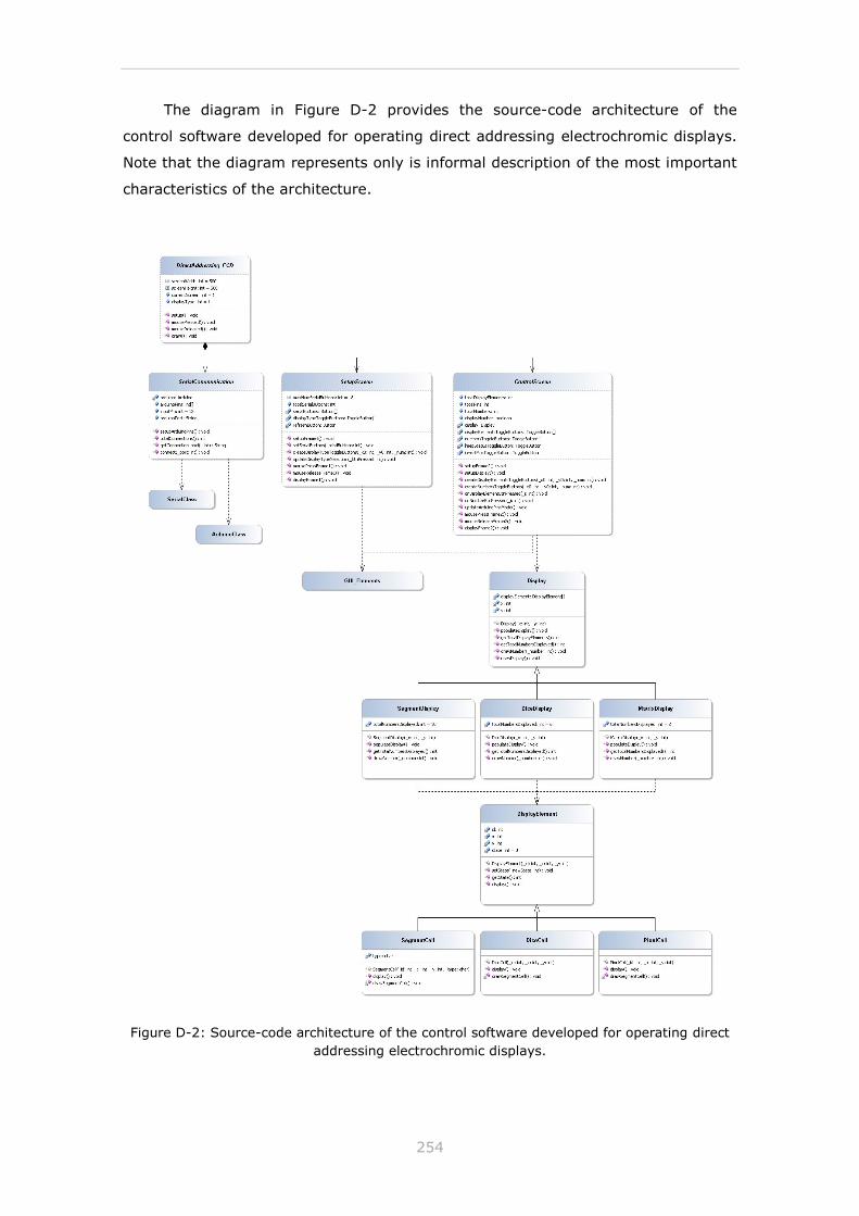
254
The diagram in Figure D-2 provides the source-code architecture of the
control software developed for operating direct addressing electrochromic displays.
Note that the diagram represents only is informal description of the most important
characteristics of the architecture.
Figure D-2: Source-code architecture of the control software developed for operating direct
addressing electrochromic displays.
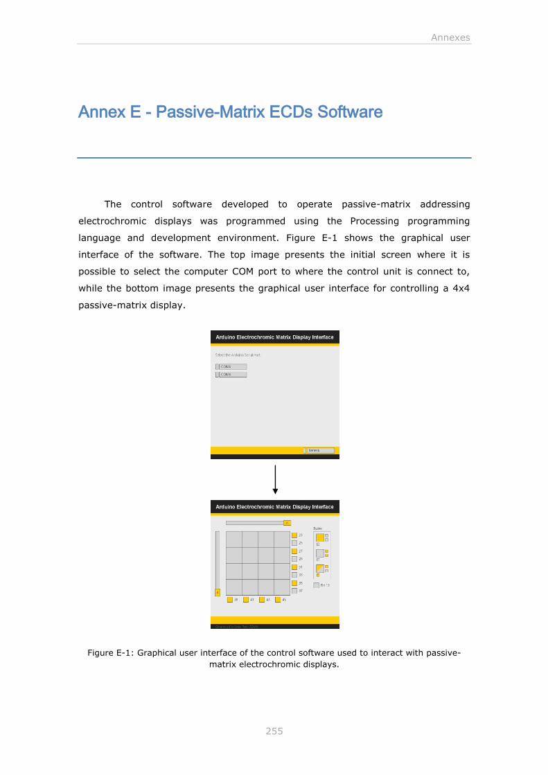
Annexes
255
Annex E - Passive-Matrix ECDs Software
The control software developed to operate passive-matrix addressing
electrochromic displays was programmed using the Processing programming
language and development environment. Figure E-1 shows the graphical user
interface of the software. The top image presents the initial screen where it is
possible to select the computer COM port to where the control unit is connect to,
while the bottom image presents the graphical user interface for controlling a 4x4
passive-matrix display.
Figure E-1: Graphical user interface of the control software used to interact with passive-
matrix electrochromic displays.
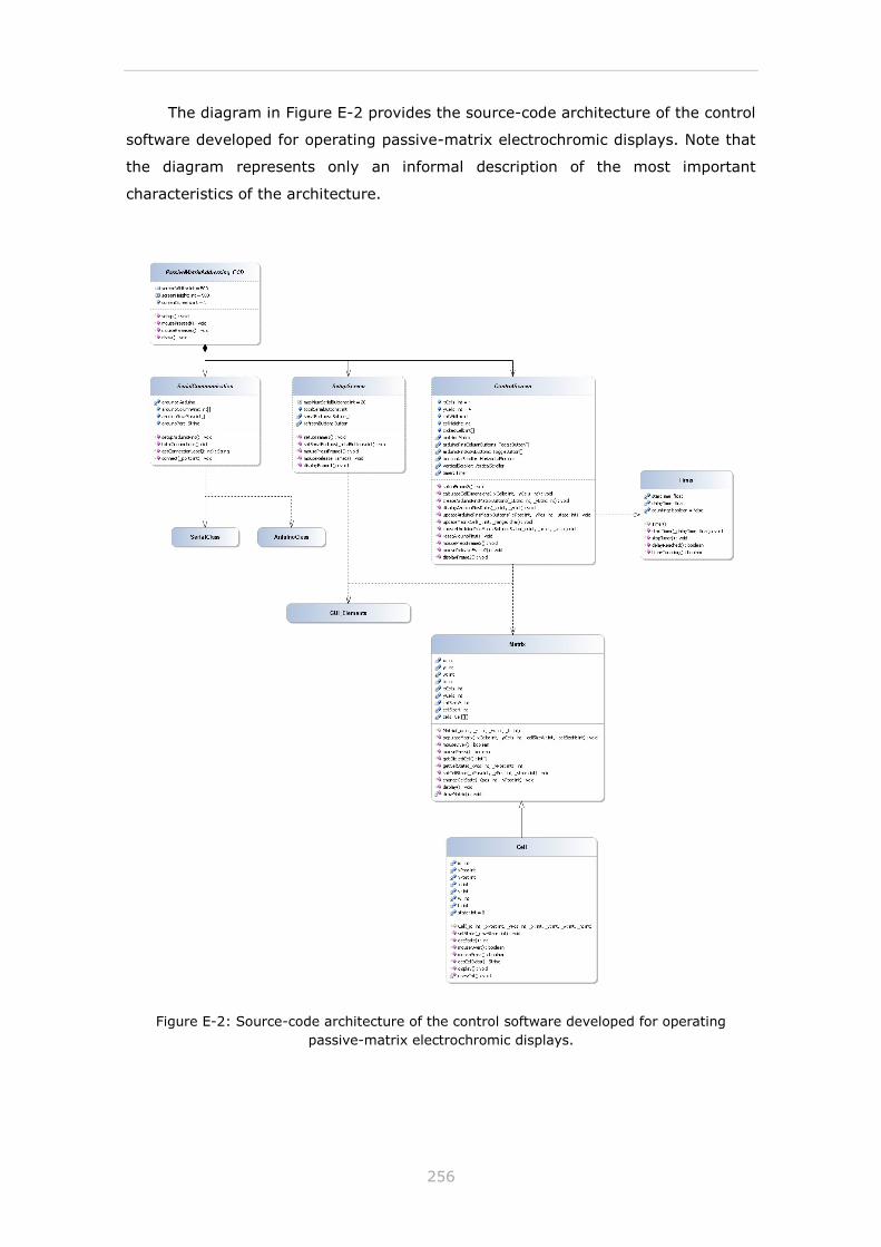
256
The diagram in Figure E-2 provides the source-code architecture of the control
software developed for operating passive-matrix electrochromic displays. Note that
the diagram represents only an informal description of the most important
characteristics of the architecture.
Figure E-2: Source-code architecture of the control software developed for operating
passive-matrix electrochromic displays.
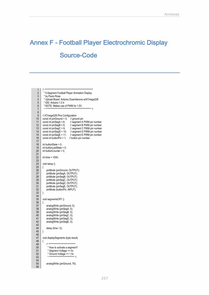
Annexes
257
Annex F - Football Player Electrochromic Display
Source-Code
1 2 3 4 5 6 7 8 9
10 11 12 13 14 15 16 17 18 19 20 21 22 23 24 25 26 27 28 29 30 31 32 33 34 35 36 37 38 39 40 41 42 43 44 45 46 47 48 49 50 51 52 53 54 55 56
/* ****************************************************** * 5-Segment Football Player Animation Display * by Paulo Rosa * Upload Board: Arduino Duamilanove w/ATmega328 * IDE: Arduino 1.0.4 * NOTE: Makes use of PWM for 1.5V * *************************************************** */ // ATmega328 Pins Configuration const int pinGround = 3; // ground pin const int pinSegA = 6; // segment A PWM pin number const int pinSegB = 5; // segment B PWM pin number const int pinSegC = 9; // segment C PWM pin number const int pinSegD = 10; // segment D PWM pin number const int pinSegE = 11; // segment E PWM pin number const int buttonPin = 1; // button pin number int buttonState = 0; int buttonLastState = 0; int buttonCounter = 0; int time = 1000; void setup () pinMode (pinGround, OUTPUT); pinMode (pinSegA, OUTPUT); pinMode (pinSegB, OUTPUT); pinMode (pinSegC, OUTPUT); pinMode (pinSegD, OUTPUT); pinMode (pinSegE, OUTPUT); pinMode (buttonPin, INPUT); void segmentsOFF () analogWrite (pinGround, 0); analogWrite (pinSegA, 0); analogWrite (pinSegB, 0); analogWrite (pinSegC, 0); analogWrite (pinSegD, 0); analogWrite (pinSegE, 0); delay (time / 3); void displaySegments (byte result) /* ****************************** * How to activate a segment? * Segment Voltage == 0v * Ground Voltage == 1.5v * **************************** */ analogWrite (pinGround, 76);
258
57 58 59 60 61 62 63 64 65 66 67 68 69 70 71 72 73 74 75 76 77 78 79 80 81 82 83 84 85 86 87 88 89 90 91 92 93 94 95 96 97 98 99
100 101 102 103 104 105 106 107 108 109 110 111 112 113 114 115 116 117 118 119 120 121 122 123 124 125 126 127 128 129 130 131 132
/* *************************************************************************** * Result must come in the form of a binary value where 1 = ON, 0 = OFF * | Seg A | Seg B | Seg C | Seg D | Seg E | * | B00001 | B00010 | B00100 | B01000 | B10000 | * ************************************************************************* */ analogWrite (pinSegA, bitRead (result, 0) == 0 ? 76 : 0); analogWrite (pinSegB, bitRead (result, 1) == 0 ? 76 : 0); analogWrite (pinSegC, bitRead (result, 2) == 0 ? 76 : 0); analogWrite (pinSegD, bitRead (result, 3) == 0 ? 76 : 0); analogWrite (pinSegE, bitRead (result, 4) == 0 ? 76 : 0); void testSegments () segmentsOFF (); displaySegments (B00001); delay (time * 5); segmentsOFF (); displaySegments (B00010); delay (time * 5); segmentsOFF (); displaySegments (B00100); delay (time * 5); segmentsOFF (); displaySegments (B01000); delay (time * 5); segmentsOFF (); displaySegments (B10000); delay (time * 5); segmentsOFF (); displaySegments (B10101); delay (time * 5); segmentsOFF (); delay (time * 5); void displayFootballPlayerSequence (int state) switch (state) case 1: displaySegments (B01101); break; case 2: displaySegments (B01110); break; case 3: displaySegments (B11010); break; default: displaySegments (B00000); void loop() // read the state of the pushbutton value: buttonState = digitalRead (buttonPin); if (buttonState != buttonLastState) if (buttonState == HIGH) buttonCounter ++; segmentsOFF (); displayFootballPlayerSequence (buttonCounter); delay (time / 2);

Annexes
259
133 134 135 136 137 138 139 140
if (buttonCounter == 4) buttonCounter = 0; buttonLastState = buttonState; // END
260
Annex G - Digital Dice Electrochromic Display
Source-Code
1 2 3 4 5 6 7 8 9
10 11 12 13 14 15 16 17 18 19 20 21 22 23 24 25 26 27 28 29 30 31 32 33 34 35 36 37 38 39 40 41 42 43 44 45 46 47 48 49 50 51 52 53 54 55 56
/* ******************************************************** * 4-Segments DIGITAL DICE Display * by Paulo Rosa * Upload Board: ATtiny85 (internal 8MHz clock) * IDE: Arduino 1.0.4 * NOTE: Requires a 1.5V Power Source * * DESCRIPTION: Random numbers are generated every * time a button is pressed * ***************************************************** */ // Pin numbers: const int buttonPin = 0; // pin number of the TiltSensor const int pinSegA = 4; // pin number of the segment A const int pinSegB = 3; // pin number of the segment B const int pinSegC = 1; // pin number of the segment C const int pinSegD = 2; // pin number of the segment D int buttonState = 0; int buttonLastState = 0; int randNumber; void setup() pinMode (buttonPin, INPUT); pinMode (pinSegA, OUTPUT); pinMode (pinSegB, OUTPUT); pinMode (pinSegC, OUTPUT); pinMode (pinSegD, OUTPUT); void setPinState (int pin, int state) // Activate de pin with the inverted result digitalWrite (pin, state == HIGH ? LOW : HIGH); void clearResult () setPinState (pinSegA, LOW); setPinState (pinSegB, LOW); setPinState (pinSegC, LOW); setPinState (pinSegD, LOW); /* **************************** * #1 = Segment B * #2 = Segment A * #3 = Segment B + D * #4 = Segment A + D * #5 = Segment A + B + D * #6 = Segment A + C + D * *************************** */ void displayResult (int result)
Annexes
261
57 58 59 60 61 62 63 64 65 66 67 68 69 70 71 72 73 74 75 76 77 78 79 80 81 82 83 84 85 86 87 88 89 90 91 92 93 94 95 96 97 98 99
100 101 102 103 104 105 106 107 108 109 110 111 112 113 114
switch (result) case 1: setPinState (pinSegB, HIGH); break; case 2: setPinState (pinSegA, HIGH); break; case 3: setPinState (pinSegB, HIGH); setPinState (pinSegD, HIGH); break; case 4: setPinState (pinSegA, HIGH); setPinState (pinSegD, HIGH); break; case 5: setPinState (pinSegA, HIGH); setPinState (pinSegB, HIGH); setPinState (pinSegD, HIGH); break; case 6: setPinState (pinSegA, HIGH); setPinState (pinSegC, HIGH); setPinState (pinSegD, HIGH); break; void loop() // read the state of the pushbutton value: buttonState = digitalRead (buttonPin); if (buttonState != buttonLastState) if (buttonState == HIGH) clearResult (); randNumber = random (1, 7); displayResult (randNumber); //digitalWrite (ledPinA, randNumber == 1 ? HIGH : LOW); //digitalWrite (ledPinB, randNumber == 2 ? HIGH : LOW); //digitalWrite (ledPinC, randNumber == 3 ? HIGH : LOW); //digitalWrite (ledPinD, randNumber == 4 ? HIGH : LOW); buttonLastState = buttonState; // END
262
Annex H - Waste Reminder Electrochromic Display
Source-Code
1 2 3 4 5 6 7 8 9
10 11 12 13 14 15 16 17 18 19 20 21 22 23 24 25 26 27 28 29 30 31 32 33 34 35 36 37 38 39 40 41 42 43 44 45 46 47 48 49 50 51 52 53 54 55 56
/* ****************************************************** * 3-Segment Waste Reminder Display * by Paulo Rosa * Upload Board: ATtiny85 (internal 8MHz clock) * IDE: Arduino 1.0.4 * NOTE: Requires a 1.5V Power Source * * DESCRIPTION: Icons are highlighted following a * pre-determined time schedule * *************************************************** */ #include <Time.h> #include <TimeAlarms.h> // Pin numbers: const int pinSegA = 4; // pin number of the segment A const int pinSegB = 3; // pin number of the segment B const int pinSegC = 2; // pin number of the segment C const int pinGround = 0; // ground pin void setup() pinMode (pinSegA, OUTPUT); pinMode (pinSegB, OUTPUT); pinMode (pinSegC, OUTPUT); pinMode (pinGround, OUTPUT); void setPinState (int pin, int state) digitalWrite (pin, state); void activateSegments (byte result) /* ******************************* * How to activate a segment? * Segment Voltage == 0v * Ground Voltage == 1.5v * ***************************** */ setPinState (pinGround, HIGH); // Activate de pin with the inverted result setPinState (pinSegA, bitRead (result, 0) == LOW ? HIGH : LOW); setPinState (pinSegB, bitRead (result, 1) == LOW ? HIGH : LOW); setPinState (pinSegC, bitRead (result, 2) == LOW ? HIGH : LOW); void reset () activateSegments (B000); void wasteAlarm()
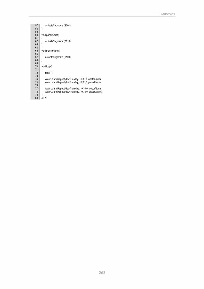
Annexes
263
57 58 59 60 61 62 63 64 65 66 67 68 69 70 71 72 73 74 75 76 77 78 79 80
activateSegments (B001); void paperAlarm() activateSegments (B010); void plasticAlarm() activateSegments (B100); void loop() reset (); Alarm.alarmRepeat(dowTuesday, 19,30,0, wasteAlarm); Alarm.alarmRepeat(dowTuesday, 19,30,0, paperAlarm); Alarm.alarmRepeat(dowThursday, 19,30,0, wasteAlarm); Alarm.alarmRepeat(dowThursday, 19,30,0, plasticAlarm); // END
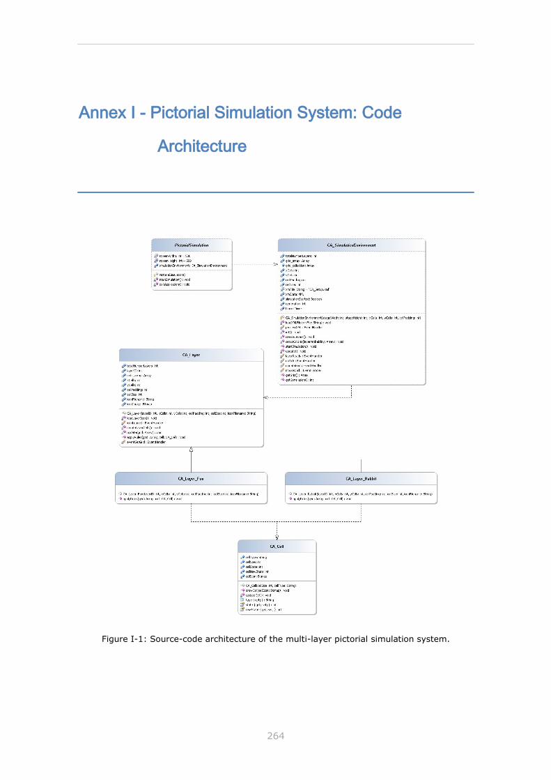
264
Annex I - Pictorial Simulation System: Code
Architecture
Figure I-1: Source-code architecture of the multi-layer pictorial simulation system.