Embed Size (px)
Citation preview
MODELING AND DESIGN OF MICROWAVE-MILLIMETERWAVE FILTERS AND MULTIPLEXERS
by
Yunchi Zhang
Dissertation submitted to the Faculty of the Graduate School of theUniversity of Maryland, College Park in partial ful�llment
of the requirements for the degree ofDoctor of Philosophy
2006
Advisory Committee:
Professor Kawthar A. Zaki, Chair/AdvisorProfessor Christopher DavisProfessor Isaak D. MayergoyzProfessor Neil GoldsmanProfessor Amr Baz


ABSTRACT
Title of dissertation: MODELING AND DESIGN OFMICROWAVE-MILLIMETERWAVEFILTERS AND MULTIPLEXERS
Yunchi Zhang, Doctor of Philosophy, 2006
Dissertation directed by: Professor Kawthar A. ZakiDepartment of Electrical and ComputerEngineering
Modern communication systems require extraordinarily stringent speci�ca-
tions on microwave and millimeter-wave components. In mobile and integrated
communication systems, miniature, ultra-wideband and high performance �lters
and multiplexers are demanded for microwave integrated circuits (MICs) and
monolithic microwave integrated circuits (MMICs). In satellite communications
and wireless base stations, small volume, high quality, high power handling capa-
bility and low cost �lters and multiplexers are required. In order to meet these re-
quirements, three aspects are mainly concerned: design innovations, precise CAD
procedure, and improved manufacturing technologies. This dissertation is, there-
fore, devoted to creating innovated �lter and multiplexer structures, developing
full-wave modeling and design procedures of �lters and multiplexers, and inte-
grating waveguide structures for MICs and MMICs in Low Temperature Co-�red
Ceramic (LTCC) technology.
In order to realize miniature and broadband �lters, novel multiple-layer cou-

pled stripline resonator structures are proposed for �lter designs. The essential of
the resonators is investigated, and the design procedure of the �lters is demon-
strated by examples. Rigorous full-wave mode matching program is developed
to model the �lters and optimize the performance. The �lters are manufactured
in LTCC technology to gain high-integration. In order to obtain better quality
than planar structures, original ridge waveguide coupled stripline resonator �lters
and multiplexers are introduced for LTCC applications. Planar and waveguide
structures are combined in such �lter and multiplexer designs to improve the loss
performance. A rigorous CAD procedure using mode matching technique is de-
veloped for the modeling and design. To design wideband multiplexers for LTCC
applications, ridge waveguide divider junctions are presented to achieve wideband
matching performance. Such junctions and ridge waveguide evanescent-mode �l-
ters are cascaded together to realize the multiplexer designs. The design method-
ology, e¤ects of spurious modes and LTCCmanufacturing procedure are discussed.
Some other important issues of microwave �lter and multiplexer designs addressed
in this dissertation are: (1) Systematic approximation, synthesis and design pro-
cedures of multiple-band coupled resonator �lters. Various �lter topologies are
created by analytical methods, and utilized in waveguide and dielectric resonator
�lter designs. (2) Dual-mode �lter designs in circular and rectangular waveguides.
(3) Systematic tuning procedure of quasi-elliptic �lters. (4) Improvement of �lter
spurious performance by stepped impedance resonators (SIRs). (5) Multipaction
e¤ects in waveguide structures for space applications.

MODELING AND DESIGN OF MICROWAVE-MILLIMETERWAVE FILTERS AND MULTIPLEXERS
by
Yunchi Zhang
Dissertation submitted to the Faculty of the Graduate School of theUniversity of Maryland, College Park in partial ful�llment
of the requirements for the degree ofDoctor of Philosophy
2006
Advisory Committee:
Professor Kawthar A. Zaki, Chair/AdvisorProfessor Christopher DavisProfessor Isaak D. MayergoyzProfessor Neil GoldsmanProfessor Amr Baz

c Copyright by
Yunchi Zhang
2006

DEDICATION
To my parents and Ningning.
ii

ACKNOWLEDGMENTS
I would like to express my deep and sincere gratitude to my advisor Prof.
Kawthar A. Zaki for her invaluable guidance and enthusiastic support during the
course of this work. Her wide knowledge and logical way of thinking have been of
great value for me. Her understanding, encouraging and trusting have provided
a good basis for the present thesis. My sincere thanks are due to Dr. Jorge A.
Ruiz-Cruz, Universidad Autónoma de Madrid, Spain, for his unsel�shly sharing
programs, friendly help, and valuable comments. I owe him lots of gratitude for
assisting me to understand the numerical methods. He could not even realize
how much I have learned from him. I am greatly indebted to Dr. Ali E. Atia,
president of Orbital Communications International, for his innovative ideas and
precious suggestions. The conversations with him have inspired me to think of
many interesting areas of research. I am very grateful to four other faculty mem-
bers of the University of Maryland at College Park, Dr. Christopher Davis, Dr.
Isaak D. Mayergoyz, Dr. Neil Goldsman, and Dr. Amr Baz, for serving in my
Advisory Committee. I would also like to thank Andrew J. Piloto, Kyocera Amer-
ican, for allowing me to have the opportunity to participate in his projects. Finally
and most importantly, I wish to acknowledge that this dissertation could not have
been accomplished without the love, encouragement, understanding, patience, and
devotion of my beautiful wife, Ningning Xu.
iii
Contents
Contents iv
List of Tables viii
List of Figures x
1 Introduction 1
1.1 Microwave-Millimeterwave Components . . . . . . . . . . . . . . . 1
1.2 CAD of Microwave Components . . . . . . . . . . . . . . . . . . . 4
1.2.1 Overview . . . . . . . . . . . . . . . . . . . . . . . . . . . 4
1.2.2 General Numerical Methods . . . . . . . . . . . . . . . . . 9
1.2.3 Mode Matching Method . . . . . . . . . . . . . . . . . . . 11
1.3 Practical Realization Technologies . . . . . . . . . . . . . . . . . . 18
1.4 Dissertation Objectives . . . . . . . . . . . . . . . . . . . . . . . . 22
1.5 Text Organization . . . . . . . . . . . . . . . . . . . . . . . . . . . 23
1.6 Dissertation Contributions . . . . . . . . . . . . . . . . . . . . . . 25
2 Multiple-Band Quasi-Elliptic Filters 27
2.1 Introduction . . . . . . . . . . . . . . . . . . . . . . . . . . . . . . 27
2.2 The Approximation Problem . . . . . . . . . . . . . . . . . . . . . 29
2.2.1 Problem Statement . . . . . . . . . . . . . . . . . . . . . . 29
2.2.2 Determination of Characteristic Function C(s) . . . . . . . 30
2.2.3 Determination of E(s); F (s); and P (s) . . . . . . . . . . . 37
2.2.4 Examples of Approximation Problem . . . . . . . . . . . . 39
iv

2.3 The Synthesis Problem . . . . . . . . . . . . . . . . . . . . . . . . 42
2.3.1 Problem Statement . . . . . . . . . . . . . . . . . . . . . . 42
2.3.2 Overview of Coupling Matrix Synthesis . . . . . . . . . . . 45
2.3.3 Cascaded Building-blocks . . . . . . . . . . . . . . . . . . 49
2.3.4 Synthesis Example . . . . . . . . . . . . . . . . . . . . . . 51
2.4 Hardware Implementation . . . . . . . . . . . . . . . . . . . . . . 54
2.4.1 Filter Transformation . . . . . . . . . . . . . . . . . . . . . 54
2.4.2 Filter Realization . . . . . . . . . . . . . . . . . . . . . . . 55
3 Microwave Filter Designs 57
3.1 Design Methodology . . . . . . . . . . . . . . . . . . . . . . . . . 57
3.1.1 Introduction . . . . . . . . . . . . . . . . . . . . . . . . . . 57
3.1.2 Generalized Design Approach . . . . . . . . . . . . . . . . 59
3.1.3 Determination of Couplings . . . . . . . . . . . . . . . . . 67
3.2 Miniature Double-layer Coupled Stripline Resonator Filters in LTCC
Technology . . . . . . . . . . . . . . . . . . . . . . . . . . . . . . 73
3.2.1 Introduction . . . . . . . . . . . . . . . . . . . . . . . . . . 73
3.2.2 Filter Con�guration . . . . . . . . . . . . . . . . . . . . . . 74
3.2.3 Filter Design and Modeling . . . . . . . . . . . . . . . . . 77
3.2.4 Design Examples . . . . . . . . . . . . . . . . . . . . . . . 85
3.2.5 LTCC Manufacturing E¤ects . . . . . . . . . . . . . . . . 100
3.3 Multiple-layer Coupled Resonator Filters . . . . . . . . . . . . . . 104
3.3.1 Introduction . . . . . . . . . . . . . . . . . . . . . . . . . . 104
3.3.2 Possible Resonator Structures . . . . . . . . . . . . . . . . 105
3.3.3 Equivalent Circuit Model . . . . . . . . . . . . . . . . . . . 109
3.3.4 Filter Con�guration . . . . . . . . . . . . . . . . . . . . . . 114
3.3.5 Triple-layer Coupled Stripline Resonator Filter . . . . . . . 115
3.3.6 Double-layer Coupled Hairpin Resonator Filter . . . . . . 125
3.4 Ridge Waveguide Coupled Stripline Resonator Filters . . . . . . . 132
3.4.1 Introduction . . . . . . . . . . . . . . . . . . . . . . . . . . 132
v
3.4.2 Chebyshev Filter Con�guration and Design . . . . . . . . . 134
3.4.3 Quasi-Elliptic Filter Con�guration and Design . . . . . . . 144
3.5 Dual-mode Asymmetric Filters in Circular Waveguides . . . . . . 155
3.5.1 Introduction . . . . . . . . . . . . . . . . . . . . . . . . . . 155
3.5.2 Filter Parameters . . . . . . . . . . . . . . . . . . . . . . . 158
3.5.3 Physical Implementation . . . . . . . . . . . . . . . . . . . 161
3.5.4 Measurement Results . . . . . . . . . . . . . . . . . . . . . 164
3.6 Dual-mode Quasi-Elliptic Filters in Rectangular Waveguides . . . 167
3.6.1 Introduction . . . . . . . . . . . . . . . . . . . . . . . . . . 167
3.6.2 Filter Con�guration . . . . . . . . . . . . . . . . . . . . . . 169
3.6.3 Filter Design Procedure . . . . . . . . . . . . . . . . . . . 172
3.6.4 Design Example . . . . . . . . . . . . . . . . . . . . . . . . 174
3.7 Systematic Tuning of Quasi-Elliptic Filters . . . . . . . . . . . . . 181
3.7.1 Introduction . . . . . . . . . . . . . . . . . . . . . . . . . . 181
3.7.2 Tuning Procedure . . . . . . . . . . . . . . . . . . . . . . . 183
3.7.3 Filter Tuning Example . . . . . . . . . . . . . . . . . . . . 189
4 Microwave Multiplexer Designs 201
4.1 Design Methodology . . . . . . . . . . . . . . . . . . . . . . . . . 201
4.1.1 General Theory . . . . . . . . . . . . . . . . . . . . . . . . 201
4.1.2 Full-Wave CAD in MMM . . . . . . . . . . . . . . . . . . 205
4.1.3 Hybrid CAD . . . . . . . . . . . . . . . . . . . . . . . . . 207
4.1.4 Multiport Network Synthesis . . . . . . . . . . . . . . . . . 210
4.2 Wideband Ridge Waveguide Divider-type Multiplexers . . . . . . 210
4.2.1 Introduction . . . . . . . . . . . . . . . . . . . . . . . . . . 210
4.2.2 Ridge Waveguide Divider Junction . . . . . . . . . . . . . 212
4.2.3 Ridge Waveguide Channel Filters . . . . . . . . . . . . . . 216
4.2.4 Input and Output Transitions . . . . . . . . . . . . . . . . 218
4.2.5 Diplexer Design Example . . . . . . . . . . . . . . . . . . . 220
4.2.6 Triplexer Design Example . . . . . . . . . . . . . . . . . . 223
vi
4.3 Waveguide Multiplexers for Space Applications . . . . . . . . . . 228
4.3.1 Introduction . . . . . . . . . . . . . . . . . . . . . . . . . . 228
4.3.2 Multiplexer Con�guration and Modeling . . . . . . . . . . 229
4.3.3 Multipaction Consideration . . . . . . . . . . . . . . . . . 235
4.3.4 Diplexer Example . . . . . . . . . . . . . . . . . . . . . . . 238
4.3.5 Triplexer Example . . . . . . . . . . . . . . . . . . . . . . 241
4.4 LTCC Multiplexers Using Stripline Junctions . . . . . . . . . . . 243
4.4.1 Introduction . . . . . . . . . . . . . . . . . . . . . . . . . . 243
4.4.2 Multiplexer Con�guration . . . . . . . . . . . . . . . . . . 244
4.4.3 Diplexer Example . . . . . . . . . . . . . . . . . . . . . . . 245
4.5 Wideband Diplexer Using E-plane Bifurcation Junction . . . . . . 247
4.5.1 Design Task and Diplexer Con�guration . . . . . . . . . . 247
4.5.2 Results . . . . . . . . . . . . . . . . . . . . . . . . . . . . . 251
5 Conclusions and Future Research 252
5.1 Conclusions . . . . . . . . . . . . . . . . . . . . . . . . . . . . . . 252
5.2 Future Research . . . . . . . . . . . . . . . . . . . . . . . . . . . . 253
A Generalized Transverse Resonance (GTR) Technique1 255
A.1 Introduction . . . . . . . . . . . . . . . . . . . . . . . . . . . . . . 255
A.2 Problem Statement . . . . . . . . . . . . . . . . . . . . . . . . . . 256
A.3 Field Expansion in Parallel-plate Region . . . . . . . . . . . . . . 260
A.4 Field Matching Between Regions . . . . . . . . . . . . . . . . . . 264
A.5 Characteristic System . . . . . . . . . . . . . . . . . . . . . . . . . 266
B Eigen�eld Distribution of Waveguides 268
C Coupling Integrals between Waveguides2 271
Bibliography 275
vii

List of Tables
1.1 Available commercial CAD software tools . . . . . . . . . . . . . . 11
1.2 Formulations to calculate the GSM of a generic step discontinuity. 16
2.1 Three multiple-band �lter examples in the sense of approximation.The zeros at in�nity are not counted in the item #Zero. . . . . . 39
2.2 Brief synthesis procedures of coupled resonator network and transver-sal array network. . . . . . . . . . . . . . . . . . . . . . . . . . . . 46
2.3 Formulas to select the rotation angle of a similarity transform. . . 47
3.1 Qualitative comparison between di¤erent realization technologies[35]. . . . . . . . . . . . . . . . . . . . . . . . . . . . . . . . . . . 61
3.2 Final dimensions of �lter example II. Variables have the similarde�nitions as in Fig. 3.17. All the dimensions are given in mil. . . 99
3.3 Final dimensions of the triple-layer coupled stripline resonator �lteras shown in Fig. 3.30. All the dimensions are given in mil. Thethickness of metallization strips is 0.4 mil. . . . . . . . . . . . . . 125
3.4 Final dimensions of the double-layer coupled hairpin resonator �lteras shown in Fig. 3.35(a). All the dimensions are given in mil. . . . 132
3.5 Final dimensions of the quasi-elliptic stripline resonator �lter asshown in Fig. 3.47(a). All the dimensions are given in mil. . . . . 152
3.6 Final dimensions of the quasi-elliptic dual-mode �lter as shown inFig. 3.59. All the dimensions are given in inch. . . . . . . . . . . 179
4.1 The speci�cations of a wideband diplexer. . . . . . . . . . . . . . 222
viii

4.2 The speci�cations of a wideband triplexer design using ridge waveguidedivider junctions. . . . . . . . . . . . . . . . . . . . . . . . . . . . 223
4.3 The speci�cations of a Ku band diplexer. All the interface waveguidesshould be WR75. 12 carriers are operating in the diplexer with thepower of each at 85 W. Isolation means channel to channel rejectionlevel. TR represents the operating temperature range. . . . . . . . 238
4.4 The speci�cations of a Ku band triplexer. The interface waveguidesare: WR62 for the common port and Ch. 3; WR75 for Ch. 1 and 2.Isolation means channel to channel rejection level. TR representsthe operating temperature range. . . . . . . . . . . . . . . . . . . 241
4.5 The speci�cations of a diplexer using stripline bifurcation junctionin LTCC technology. . . . . . . . . . . . . . . . . . . . . . . . . . 247
4.6 The speci�cations of a wideband diplexer using E-plane bifurcationjunction. . . . . . . . . . . . . . . . . . . . . . . . . . . . . . . . . 248
A.1 Properties of TE (h), TM (e) and TEM (o) modes of a homogeneouswaveguide cross section [10, 35]. . . . . . . . . . . . . . . . . . . . 257
A.2 Basis functions for TEM, TE and TM modes. . . . . . . . . . . . 262
ix

List of Figures
1.1 An example of satellite payload system. . . . . . . . . . . . . . . . 3
1.2 (a) Physical layout of a coupled microstrip line �lter. (b) The layoutof (a) has been subdivided using the standard library elements foranalysis. . . . . . . . . . . . . . . . . . . . . . . . . . . . . . . . . 7
1.3 (a) 3D structure of a combline �lter. (b) Subdivided circuits of (a)for analysis. (reprinted from the archived seminar in Ansoft.com.) 8
1.4 Examples of non-canonical waveguide geometries that can be ana-lyzed by mode matching method. . . . . . . . . . . . . . . . . . . 13
1.5 (a) A generic step discontinuity structure that can be characterizedby GSM. (b) A generic multiple-port junction structure that canbe characterized by GAM. . . . . . . . . . . . . . . . . . . . . . . 14
1.6 (a) An example of components consisting of only step discontinu-ities. (b) An example of components using multiple-port junctions. 17
2.1 Low-pass prototype multiple-band �lter . . . . . . . . . . . . . . . 32
2.2 A typical curve of the characteristic function with the critical fre-quency points . . . . . . . . . . . . . . . . . . . . . . . . . . . . . 34
2.3 The approximation example 1 with prescribed complex zeros. . . . 40
2.4 Magnitude response of the approximation example 2. . . . . . . . 41
2.5 Magnitude response of the approximation example 3. . . . . . . . 42
2.6 The synthesized starting networks for a multiple-band �lter. (a)Coupled Resonator Network. (b) Compact notation of coupled res-onator network. (c) Transversal array network in compact notation. 44
x
2.7 Well-known �lter topologies. (a) Canonical folded network for sym-metric cases (even and odd orders). (b) Canonical folded networkfor asymmetric cases (even and odd orders). (c) Extented-box sec-tions (three cases). (d) Cul-De-Sac (three cases). (e) CascadedTriplets. (f) Cascaded Quartets. (g) Cascaded N-tuplets. (h) In-line topology. . . . . . . . . . . . . . . . . . . . . . . . . . . . . . 48
2.8 One transformation example using the building block technique.(a) Diagram from cascaded triplets to cascaded quintets. (b) Thesequential rotations. . . . . . . . . . . . . . . . . . . . . . . . . . 50
2.9 Wheel network topology for an Nth order �ltering function withM transmission zeros. It can be transformed to CT topology ana-lytically. . . . . . . . . . . . . . . . . . . . . . . . . . . . . . . . . 51
2.10 A multiple-band �lter synthesis example. (a) Magnitude responseof the multiple-band �ltering function (6 poles and 3 zeros) in nor-malized frequency. (b) Possible network topologies: folded network;Cul-De-Sac network; Cascaded Triplets network; Cascaded Quartetand Triplet network. . . . . . . . . . . . . . . . . . . . . . . . . . 53
3.1 The �ow chart of generalized �lter design procedure. . . . . . . . 60
3.2 Low-pass �lter prototypes. (a) Unit elements with series inductors.(b) Unit elements with parallel capacitors. (c) Cascade of unitelements. . . . . . . . . . . . . . . . . . . . . . . . . . . . . . . . . 62
3.3 Inter-coupling between coupled resonators. (a) Coupled resonatorcircuit with electric coupling. (b) Coupled resonator circuit withmagnetic coupling. (c) Coupled resonator circuit with mixed elec-tric and magnetic coupling. . . . . . . . . . . . . . . . . . . . . . 68
3.4 (a) Two-port scattering matrix of a lossless, reciprocal microwavecoupling structure. (b) A circuit representation of the couplingstructure by k-inverter and transmission lines. . . . . . . . . . . . 70
3.5 (a) An equivalent circuit of the input/output resonator with anexternal coupling resistance. (b) Typical phase response and phasevariation response of the re�ection coe¢ cient S11. . . . . . . . . . 72
3.6 Double-layer coupled stripline resonator structure. (a) 3D view.(b) Cross section. (c) Side view. The structure is �lled with ahomogeneous dielectric material. . . . . . . . . . . . . . . . . . . . 75
3.7 Filter con�gurations using double-layer coupled stripline resonators.(a) Interdigital �lter con�guration. (b) Combline �lter con�guration. 76
xi
3.8 Inter-coupling curves of interdigital and combline con�gurations.Identical resonators are used. S is the separation between tworesonators. . . . . . . . . . . . . . . . . . . . . . . . . . . . . . . . 77
3.9 A 10th order interdigital �lter using double-layer coupled striplineresonators. (a) Physical structrure with ports along z-axis. (b)Involved cross sections of structure in (a) along z-axis. (c) Physicalstructrure with ports bent along x-axis. (d) Involved cross sectionsof structure in (c) along x-axis. . . . . . . . . . . . . . . . . . . . 80
3.10 An odd-order (11th) interdigital �lter using double-layer coupledstripline resonators. . . . . . . . . . . . . . . . . . . . . . . . . . . 83
3.11 The end view along x-direction of the �lter con�guration in Fig.3.9(c). . . . . . . . . . . . . . . . . . . . . . . . . . . . . . . . . . 86
3.12 (a) Con�guration to decide the dimensions of the resonator. (b)Typical frequency response of S21 for con�guration (a). . . . . . . 87
3.13 (a) The con�guration to calculate the external coupling R. (b)External coupling curve: normalized R vs tapped-in position htapin 89
3.14 (a) The con�guration to calculate the inter-coupling between tworesonators. (b) The typical simulated magnitude and phase re-sponses of con�guration (a). . . . . . . . . . . . . . . . . . . . . . 90
3.15 Inter-coupling curve between two resonators: normalized couplingm vs separation S. . . . . . . . . . . . . . . . . . . . . . . . . . . 91
3.16 (a) Frequency response of �lter example I with initial dimensions.(b) Simulated frequency response of �lter example I with �nal di-mensions by HFSS and MMM with only TEM modes. . . . . . . . 92
3.17 The �nal dimensions of �lter example I: widths of the resonators(in mil): ws1 = 21:2, ws2 = 23:1, ws3 = 21:4, ws4 = 20:2, ws5 =19:8. Separations between resonators (in mil): s1 = 7:2, s2 =11, s3 = 12:4, s4 = 13:1, s5 = 13:4. Other dimensions (in mil):lr = 500, lc = 420, htapin = 434, wtapin = 19. Ports are 50ohmstriplines. The �lter is �lled with a homogeneous dielectric materialwith "r = 5:9. The vertical dimensions shown in Fig. 3.11 are givenin the context. . . . . . . . . . . . . . . . . . . . . . . . . . . . . . 93
3.18 (a) Picture of the measurement arrangement. (b) Picture of themanufactured �lters (example I and II). Filter II is slightly largerthan Filter I. . . . . . . . . . . . . . . . . . . . . . . . . . . . . . 95
xii

3.19 (a) Measured frequency response of �lter I. (b) Comparison betweenthe measurement and the simulated response by HFSS. . . . . . . 96
3.20 (a) Measured response of �lter II. (b) Comparison between themeasurement and the simulated response by HFSS. . . . . . . . . 98
3.21 (a) Structure of combline �lter example III. (b) Frequency responseby HFSS. Filter dimensions: h1 = 29:68mil, h2 = 37:08mil, h =63:02mil, (as in Fig. 3.11). w1 = 21:8mil, w2 = 20mil, w3 =20mil, s1 = 23:06mil, s2 = 30:6mil, s3 = 31:7mil, lr = 700mil,lc = 516mil, htapin = 322:7mil, wtapin = 20mil, aport = 100mil. 101
3.22 Draft of the physical realization of �lters in LTCC technology. . . 102
3.23 Possible multiple-layer coupled resonator structures. (a) Doubleand triple layer stripline resonators. Each strip is grounded at oneend. (b) Double and triple layer hairpin resonators. (c) Double andtriple layer folded stripline resonators. (d) Double and triple layerspiral resonators. . . . . . . . . . . . . . . . . . . . . . . . . . . . 106
3.24 Comparison between resonators with di¤erent number of layers. (a)One-layer stripline resonator. (b) Double-layer coupled striplineresonator. (c) Triple-layer coupled stripline resonator. . . . . . . . 108
3.25 The equivalent circuit model of multiple-layer coupled resonators.(a) Single-layer resonator. (b) Double-layer coupled resonator. (c)Triple-layer coupled resonator. (d) Equivalent circuit of n-layercoupled resonator. . . . . . . . . . . . . . . . . . . . . . . . . . . . 110
3.26 Natural resonant frequencies of multiple-layer coupled resonators.(a) Single-layer stripline resonator. (b) Double-layer coupled striplineresonator with two natural resonant frequencies. (c) Triple-layercoupled stripline resonator with three natural resonant frequencies. 113
3.27 A triple-layer coupled stripline resonator (Drawings are not in scale).(a) 3D view with excitations. (b) End view. (c) Side view. (d)Typical S21 response. . . . . . . . . . . . . . . . . . . . . . . . . . 117
3.28 External coupling structure and computed coupling curves. (a)Tapped-in stripline external coupling structure. (b) External cou-pling curves with respect to the tapped-in position htap. . . . . . 119
3.29 Inter-coupling structure and coupling curves. (a) Interdigital cou-pling structure between resonators. (b) Inter-coupling curves vsseparation s. . . . . . . . . . . . . . . . . . . . . . . . . . . . . . . 120
xiii
3.30 Filter structure using triple-layer coupled stripline resonators. The�lter is �ipped-symmetric and �lled with homogeneous dielectricmaterials. (a) 3D view of the �lter. (b) Top view of the �lter withde�ned variables. . . . . . . . . . . . . . . . . . . . . . . . . . . . 122
3.31 Frequency response of the initial �lter structure by Sonnet. . . . . 123
3.32 Frequency response of the �nal �lter design by Sonnet. (a) In-bandresponse. (b) Wide band response. . . . . . . . . . . . . . . . . . 124
3.33 (a)Structure of double-layer coupled hairpin resonator (Filled withhomogeneous dielectric material). (b) Resonant frequency f0 withrespect to the resonator length lr. . . . . . . . . . . . . . . . . . 127
3.34 (a) External coupling curve of a tapped-in structure. (b) Inter-coupling curve between two double-layer coupled hairpin resonators.. . . . . . . . . . . . . . . . . . . . . . . . . . . . . . . . . . . . . 129
3.35 (a) A six-pole interdigital �lter structure using double-layer coupledhairpin resonators. (b) The frequency response of the �lter withinitial dimensions. . . . . . . . . . . . . . . . . . . . . . . . . . . . 130
3.36 The frequency response of the �nal �lter design using double-layercoupled hairpin resonators. (a) In-band response. (b) Wide bandresponse. . . . . . . . . . . . . . . . . . . . . . . . . . . . . . . . . 131
3.37 (a) Chebyshev �lter con�guration using ridge waveguide coupledstripline resonators for LTCC applications. (b) Draft of LTCCphysical realization of a segment of the �lter structure as shown in(a) (Stripline-Ridge-Stripline). . . . . . . . . . . . . . . . . . . . . 135
3.38 (a) Two types of cross sections that appear in the Chebyshev �ltercon�guration: Stripline and Ridge waveguide. (b) Stripline tapped-in excitation for the external coupling. (c) Inter-coupling sectionbetween two stripline resonators by evanescent ridge waveguide. . 137
3.39 Inter-coupling values between stripline resonators with respect tothe length lr of the ridge waveguide coupling section. Other di-mensions are given in Fig. 3.40. . . . . . . . . . . . . . . . . . . . 140
3.40 (a) Filter structure and dimensions. (b) Simulated frequency re-sponse by MMM and HFSS. Dimensions (in mil) of the �lter are:a = 100, b = 37:4, d = 29:92, ws0 = 7, ws1 = 20, w = 45,ls1 = 40:88, ls2 = 79:66, l1 = l13 = 44:73, l2 = l12 = 192:12, l3 =l11 = 63:37, l4 = l10 = 189:38, l5 = l9 = 76:25, l6 = l8 = 188:9,l7 = 78:92. . . . . . . . . . . . . . . . . . . . . . . . . . . . . . . . 141
xiv
3.41 Frequency response with lossy material (conductivity � = 13100000S/m and loss tangent is 0.002). . . . . . . . . . . . . . . . . . . . 142
3.42 (a) Filter structure using SIRs. (b) Frequency response by MMMand HFSS. Filter dimensions (in mil) are: a = 100, b = 37:4,d = 29:92, ws0 = 7, ws1 = 20, w = 45, wsh = 80, ls1 = 33:99,ls2 = 87:65, lh = 30, ll1 = 87:83, ll2 = 87:03, ll3 = 85:92, l1 =46:33; l2 = 147:83, l3 = 66:99, l4 = 147:03, l5 = 80:4, l6 = 145:92,l7 = 84:26. The length of narrow striplines in all the resonators aresame as lh. . . . . . . . . . . . . . . . . . . . . . . . . . . . . . . 143
3.43 (a) Physical con�guration of canonical �lter topology using striplineresonators. (b) Canonical topology of 2n resonator symmetric quasi-elliptic �lter. . . . . . . . . . . . . . . . . . . . . . . . . . . . . . . 145
3.44 (a) Con�guration of electric cross coupling. (b) Con�guration ofmagnetic cross coupling. . . . . . . . . . . . . . . . . . . . . . . . 147
3.45 Two types of new cross sections in the canonical �lter con�guration.(a) Symmetric double stripline waveguide. (b) Symmetric doubleridge-stripline waveguide. . . . . . . . . . . . . . . . . . . . . . . . 148
3.46 The cross coupling curves. (a) Electric cross coupling curve M14
and loaded frequency f0 as a function of wi1 (lc1 = wi1� 20mil).(b) Magnetic cross coupling curve M23 and loaded frequency f0 asa function of wi2 (wr2 = 0:45 � wi2). Other dimensions are shownin Table 3.5. . . . . . . . . . . . . . . . . . . . . . . . . . . . . . . 151
3.47 (a) The whole �lter structure (Filled with LTCC ceramics "r = 5:9).(b) Simulated �lter resonse by MMM with the initial dimensions. 153
3.48 (a) Simulated frequency response of the �nal �lter design by MMMand HFSS. Response obtained from ideal circuit model is also shownfor comparison. (b) Wide band frequency response by MMM. . . 154
3.49 Network topologies applicable for dual-mode �lter designs. (a)Canonical folded-network for symmetric transfer function. (b) Extended-box or longitudinal network for symmetric transfer function. (c)Extended-box or longitudinal network for asymmetric transfer func-tion. . . . . . . . . . . . . . . . . . . . . . . . . . . . . . . . . . . 156
3.50 Ideal response of a 4-pole-1-zero asymmetric quasi-elliptic �lter. (a)Transmission zero within the upper stopband. (b) Transmissionzero within the lower stopband. . . . . . . . . . . . . . . . . . . . 159
xv

3.51 (a) The implementation structure for the 4th-order longitudinaltopology in dual-mode circular waveguide cavities. (b) The sep-arated parts of the manufactured �lter. (c) The assembled �lterhardware. . . . . . . . . . . . . . . . . . . . . . . . . . . . . . . . 162
3.52 Front view and side view of the coupling iris. . . . . . . . . . . . . 163
3.53 Measured �lter responses of dual-mode circular wavguide �lter. (a)Transmission zero within the upper stopband. (b) Transmissionzero within the lower stopband. . . . . . . . . . . . . . . . . . . . 165
3.54 Photograph of the dual-mode circular waveguide cavity �lter on thetest bench. . . . . . . . . . . . . . . . . . . . . . . . . . . . . . . . 166
3.55 (a) Physical con�guration of a rectangular waveguide quasi-ellipticfunction dual-mode �lter. (b) Cross coupling mechanism betweenthe dual modes. . . . . . . . . . . . . . . . . . . . . . . . . . . . . 170
3.56 External coupling structure and calculated coupling curve. (a) Cou-pling structure and dimensions. (b) Coupling curves: k vs widthof iris, and phase o¤sets vs width of iris. . . . . . . . . . . . . . . 175
3.57 (a) Inter-coupling structure and dimensions. (b) Inter-couplingcurves: inverter values vs cross sections of iris. . . . . . . . . . . . 177
3.58 Cross coupling structure for dual-mode waveguide �lter and thecalculated coupling curves. (a) Coupling structure and dimensions.(b) Coupling curves: coupling value M and loaded frequency f0 vslength of small waveguide lcrs. . . . . . . . . . . . . . . . . . . . 178
3.59 (a) Frequency response of the �lter with initial dimensions. (b)Frequency responses of the ideal circuit model and the �nal �lterstructure in MMM and HFSS. . . . . . . . . . . . . . . . . . . . 180
3.60 The ideal response of a quasi-elliptic eight-pole �lter with two �nitetransmission zeros. The �lter is synthesized in Cul-De-Sac topology. 190
3.61 Dielectric resonator structure. (a) Top view. (b) Side view. (c)Dielectric resonator with tuning disc. . . . . . . . . . . . . . . . . 191
3.62 The coupling structures for dielectric resonator �lters. (a) A curvedprobe for external coupling. (b) A straight wire for external cou-pling. (c) Iris coupling structure for positive coupling. (d) Curvedprobe structure for positive coupling. (e) Straight wire structure fornegative coupling. (f) Curved probe structure for negative coupling. 193
xvi
3.63 The phase of the re�ection coe¢ cient of the in-line diagnosis path.(a) Path L-8. (b) Path L-8-7. (c) Path L-8-7-3. (d) Path L-8-7-3-4. 195
3.64 The phase of the re�ection coe¢ cient of the in-line diagnosis paths.(a) Path L-8-7-3-2. (b) Path L-8-7-6. (c) Path L-8-7-6-5. (d) PathS-1-2-6. . . . . . . . . . . . . . . . . . . . . . . . . . . . . . . . . 196
3.65 The phase response of the sub-�lters in the �lter structure. (a) Sub-�lter path S-1-2-6-5. (b) Sub-�lter path S-1-2-6-5-3. (c) Sub-�lterpath S-1-2-6-5-3-4. (d) Sub-�lter path S-1-2-6-5-3-4-7. . . . . . . . 198
3.66 (a) The measured response of the pre-tuned �lter. (b) The mea-sured response of the �ne-tuned �lter. . . . . . . . . . . . . . . . . 199
4.1 The typical response of a singly terminated quasi-elliptic �lter. (a)Real and imaginary parts of input admittance Yin. (b) S-parameters.204
4.2 A hybrid CAD model of a manifold multiplexer. The channel �ltersmay be represented by circuit models or S-parameters from an EMsimulator. . . . . . . . . . . . . . . . . . . . . . . . . . . . . . . . 208
4.3 (a) Structure of a simple ridge waveguide divider junction. (b) Atypical magnitude response of the junction. . . . . . . . . . . . . . 213
4.4 (a) Structure of a ridge waveguide divider junction with an embed-ded matching transformer. (b) Typical magnitude response of theimproved divider junction. . . . . . . . . . . . . . . . . . . . . . . 215
4.5 (a) A typical ridge waveguide evanescent-mode �lter. (b) Cou-pling by evanescent rectangular waveguide. (c) Coupling by evanes-cent narrow ridge waveguide. (d) Coupling between �ipped ridgewaveguides by evanescent rectangular waveguide. . . . . . . . . . 217
4.6 (a) A transition from ridge waveguide to 50 ohm stripline in LTCC.(b) A transition from ridge waveguide to SMA connector. (c) Sim-ulation and measurement results of a back-to-back transition inLTCC. . . . . . . . . . . . . . . . . . . . . . . . . . . . . . . . . . 219
4.7 (a) Structure of channel �lter 1. (b) Structure of channel �lter 2 in-cluding transformer in-front. (c) Diplexer structure and simulatedresponse in MMM and HFSS. . . . . . . . . . . . . . . . . . . . . 221
4.8 Triplexer con�guration by cascading two diplexers using ridge waveguidedivider junctions. . . . . . . . . . . . . . . . . . . . . . . . . . . . 224
xvii

4.9 (a) side view of diplexer 1 for the triplexer design. (b) Simulatedresponse of diplexer 1 by MMM and HFSS. . . . . . . . . . . . . . 225
4.10 (a) Side view of diplexer 2 for the triplexer design. (b) Simulatedresponse of diplexer 2 by MMM and HFSS. . . . . . . . . . . . . . 226
4.11 (a) Side view of the triplexer structure ful�lled by two cascadeddiplexers. (b) Simulated response in MMM. . . . . . . . . . . . . 227
4.12 (a) E-plane waveguide T-junction. (b) Multiplexer con�guration. . 230
4.13 The �lter structures employed in the multiplexers. (a) Stepped im-pedance waveguide lowpass �lter. (b) Waveguide inductive windowbandpass �lter. (c) Waveguide lowpass �lter with E-plane roundcorners. (d) Waveguide bandpass �lter with E-plane round corners. 231
4.14 Approximation of round corner by waveguide steps for analysis. . 233
4.15 (a) The Ku-band diplexer structure. (b) The simulated diplexerresponse in MMM and HFSS. . . . . . . . . . . . . . . . . . . . . 239
4.16 (a) The Ku-band Triplexer structure. (b) The simulated responsesin MMM and HFSS. . . . . . . . . . . . . . . . . . . . . . . . . . 242
4.17 (a) Stripline bifurcation junction. (b) Stripline manifold junctioncomposed of stripline T-junctions. (c) Ridge waveguide coupledstripline resonator �lter. . . . . . . . . . . . . . . . . . . . . . . . 245
4.18 (a) Diplexer structure. (b) Simulated responses in MMM. . . . . . 246
4.19 (a) E-plane waveguide bifurcation junction. (b) Simulated responseof the junction. (c) Ridge waveguide �lter structure with transform-ers. (d) Iris coupled waveguide �lter structure. . . . . . . . . . . . 249
4.20 (a) The diplexer structure. (b) Simulated responses in MMM andHFSS. . . . . . . . . . . . . . . . . . . . . . . . . . . . . . . . . . 250
A.1 (a) Generic waveguide cross-section that can be characterized byGTR. (b) Generalized equivalent transverse network of the genericcross-section. Dm represents the discontinuity between two parallel-plate regions. Dm is characterized by GSM. . . . . . . . . . . . . 259
A.2 (a) One single-parallel-plate region with two reference systems. (b)One multi-parallel-plate region consisting of T subregions. . . . . 260
xviii
A.3 (a) Basic discontinuity between two parallel-plate regions. A sim-pli�ed reference system is used. (b) An equivalent block model.The discontinuity is represented by GSMx. . . . . . . . . . . . . . 264
B.1 Electric �eld distribution of waveguides. (a) TEMmode of stripline.(b) Fundamental mode of coupled-ridge. (c) Fundamental mode ofsingle ridge. (d) Fundamental mode of double ridge. (e) Two TEMmodes of multiple-stripline (totally 20 TEM modes exist). . . . . 269
B.2 Electric �eld distribution of waveguides. (a) TEMmode with PMWof coupled stripline. (b) TEMmode with PEW of coupled stripline.(c) TEM mode with PMW of ridge-stripline. (d) TEM mode withPEW of ridge-stripline. (e) The �rst TE mode with PMW of ridge-stripline. (f) The �rst TE mode with PEW of ridge-stripline. . . . 270
xix
Chapter 1
Introduction
1.1 Microwave-Millimeterwave Components
Microwave and millimeter-wave bands have been widely employed for many com-
mercial and military applications such as radar systems, communication systems,
heating systems, and medical imaging systems, etc. Radar systems are used for de-
tecting, locating and sensing remote targets. Examples of some radar systems are
air-tra¢ c control systems, missile tracking radars, automobile collision-avoidance
systems, weather prediction systems, and motion detectors. Communication sys-
tems have been developed rapidly in recent years in order to support a wide vari-
ety of applications. Examples of communication systems include direct broadcast
satellite (DBS) television, personal communications systems (PCSs), wireless lo-
cal area networks (WLANs), global positioning systems (GPSs), cellular phone
and video systems, and local multipoint distribution systems (LMDS).
Microwave and millimeter-wave components are required in all the afore-
1
mentioned systems. Typical components are [1�3]: �lters, multiplexers, couplers,
transformers, polarizers, orthomode transducers (OMTs), power dividers, circu-
lators, switches, low noise ampli�ers (LNAs), frequency synthesizers, power am-
pli�ers, and oscillators. In order to illustrate the basic functions of these compo-
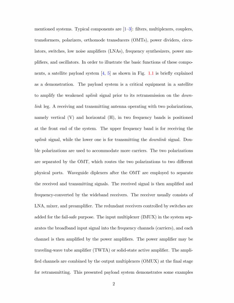
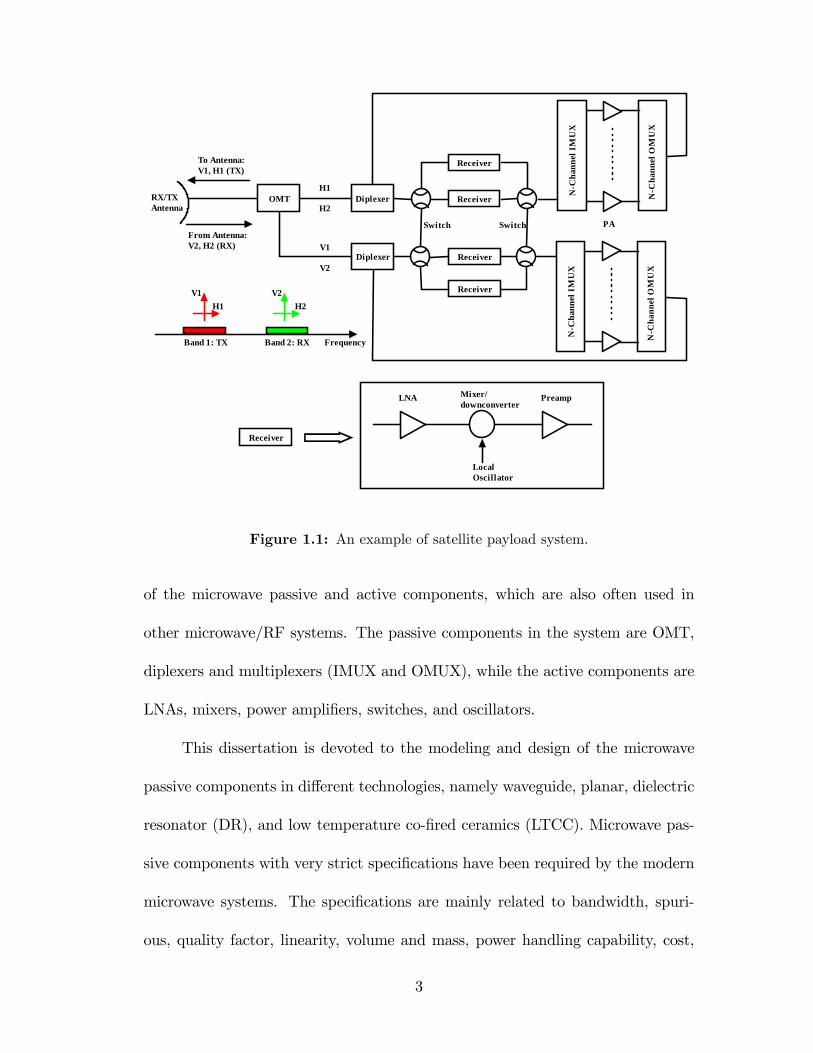
nents, a satellite payload system [4, 5] as shown in Fig. 1.1 is brie�y explained
as a demonstration. The payload system is a critical equipment in a satellite
to amplify the weakened uplink signal prior to its retransmission on the down-
link leg. A receiving and transmitting antenna operating with two polarizations,
namely vertical (V) and horizontal (H), in two frequency bands is positioned
at the front end of the system. The upper frequency band is for receiving the
uplink signal, while the lower one is for transmitting the downlink signal. Dou-
ble polarizations are used to accommodate more carriers. The two polarizations
are separated by the OMT, which routes the two polarizations to two di¤erent
physical ports. Waveguide diplexers after the OMT are employed to separate
the received and transmitting signals. The received signal is then ampli�ed and
frequency-converted by the wideband receivers. The receiver usually consists of
LNA, mixer, and preampli�er. The redundant receivers controlled by switches are
added for the fail-safe purpose. The input multiplexer (IMUX) in the system sep-
arates the broadband input signal into the frequency channels (carriers), and each
channel is then ampli�ed by the power ampli�ers. The power ampli�er may be
traveling-wave tube ampli�er (TWTA) or solid-state active ampli�er. The ampli-
�ed channels are combined by the output multiplexers (OMUX) at the �nal stage
for retransmitting. This presented payload system demonstrates some examples
2
OMT
Diplexer
Diplexer
Receiver
Receiver
Receiver
Receiver
PA
To Antenna:V1, H1 (TX)
From Antenna:V2, H2 (RX)
RX/TXAntenna
Switch Switch
H1
H2
V1
V2
NC
hann
elIM
UX
NC
hann
elO
MU
X
NC
hann
elIM
UX
NC
hann
elO
MU
X
LocalOscillator
LNA Mixer/downconverter
Preamp
Receiver
Band 1: TX Band 2: RX Frequency
V1H1
V2H2
Figure 1.1: An example of satellite payload system.
of the microwave passive and active components, which are also often used in
other microwave/RF systems. The passive components in the system are OMT,
diplexers and multiplexers (IMUX and OMUX), while the active components are
LNAs, mixers, power ampli�ers, switches, and oscillators.
This dissertation is devoted to the modeling and design of the microwave
passive components in di¤erent technologies, namely waveguide, planar, dielectric
resonator (DR), and low temperature co-�red ceramics (LTCC). Microwave pas-
sive components with very strict speci�cations have been required by the modern
microwave systems. The speci�cations are mainly related to bandwidth, spuri-
ous, quality factor, linearity, volume and mass, power handling capability, cost,
3

and development time. For example, high integration of microwave integrated
circuits (MICs) and monolithic microwave integrated circuits (MMICs) requires
miniature and broadband �lters and multiplexers. Wireless base station requests
�lters and multiplexers with small volume, low loss, high power handling capabil-
ity and high rejection levels. Satellite communication systems need multiplexers
with many channels and very small guarding bandwidth. The objective of this
dissertation is to provide some new ideas for the design of the microwave passive
components with very strict speci�cations.
1.2 CAD of Microwave Components
1.2.1 Overview
Computer aided design (CAD) of microwave components has advanced steadily
over the past few decades with the development of the computers. Many versatile
CAD tools have been developed, and are being used to all kinds of the microwave
component designs. The main purpose of CAD is to obtain the physical dimen-
sions of a component with the prescribed speci�cations, and reduce or even avoid
the experimental debugging and tuning period after the manufacture of the com-
ponent. The �nal objective is, actually, to shorten the development time and
reduce the total cost. However, not all the components used nowadays, especially
the ones with very demanding speci�cations, can be designed optimally and e¢ -
ciently by the available CAD tools. The development of e¢ cient CAD tools is,
4
therefore, still a very active research area.
The traditional CAD methods are based on the equivalent circuit theory,
which were �rst used by the members of the radiation laboratory of the Massa-
chusetts Institute of Technology (MIT) for the design of microwave components
[6�8]. The circuit-theory-based CAD introduces single (fundamental) mode equiv-
alent circuits to represent complex waveguide discontinuities in terms of simple
lumped circuit elements (inductors, capacitors, transformers, and resistors, etc.).
The complex electromagnetic �eld problems can then be solved with simple cal-
culations based on the network theory, and the computational e¤ort required to
obtain the �nal results is negligible. Many equivalent circuit models for waveguide
discontinuities and junctions can be found in [7]. These models, together with the
network synthesis theory [9], have been applied for the design of many devices.
Although single mode equivalent networks have proved to be very valuable
engineering tools, they also have serious drawbacks [3, 10, 11]. The most impor-
tant one is that equivalent circuit models only take the fundamental mode of the
waveguide into account to represent the distributed discontinuities in terms of
lumped elements. However, the discontinuities in close proximity usually excite
many higher order modes that are not considered in the equivalent circuit models.
Thus, the single mode equivalent networks are no longer valid for these cases. In
reality, the designed prototypes using the equivalent circuit theory usually need
more experimental debugging and tuning.
Field-theory-based CAD or full-wave analysis of microwave components is
an alternative to the previous circuit-theory-based approach. Basically, the �eld-
5

theory-based CAD tools are created based on the direct or approximate solution
of Maxwell�s equations [12�15]. The development of the computers has allowed
the realization of many numerical �eld-solvers that seemed not feasible many
years ago because of the lack of the computational power. The �eld-theory-based
approach is superior to the circuit-theory-based one because i) it predicts very
accurate frequency response; ii) it takes higher order mode e¤ects into account;
iii) it can potentially include all the electromagnetic e¤ects: radiation, excitation,
and loss, etc.; iv) it can be used to calculate and observe the �eld distribution in
components; v) it is valid for any frequency or wavelength range; vi) it can be de-
veloped to analyze a discontinuity with an arbitrary shape. The most signi�cant
limitation on �eld-solver tools is the long solution time to analyze a complex com-
ponent given the available computer resources: Central Processing Unit (CPU)
speed, memory amount, and disk storage. Many researchers are now working on
developing e¢ cient algorithms to speed up the simulation of �eld-solver tools.
When lengthy simulation prevents one from analyzing complete components
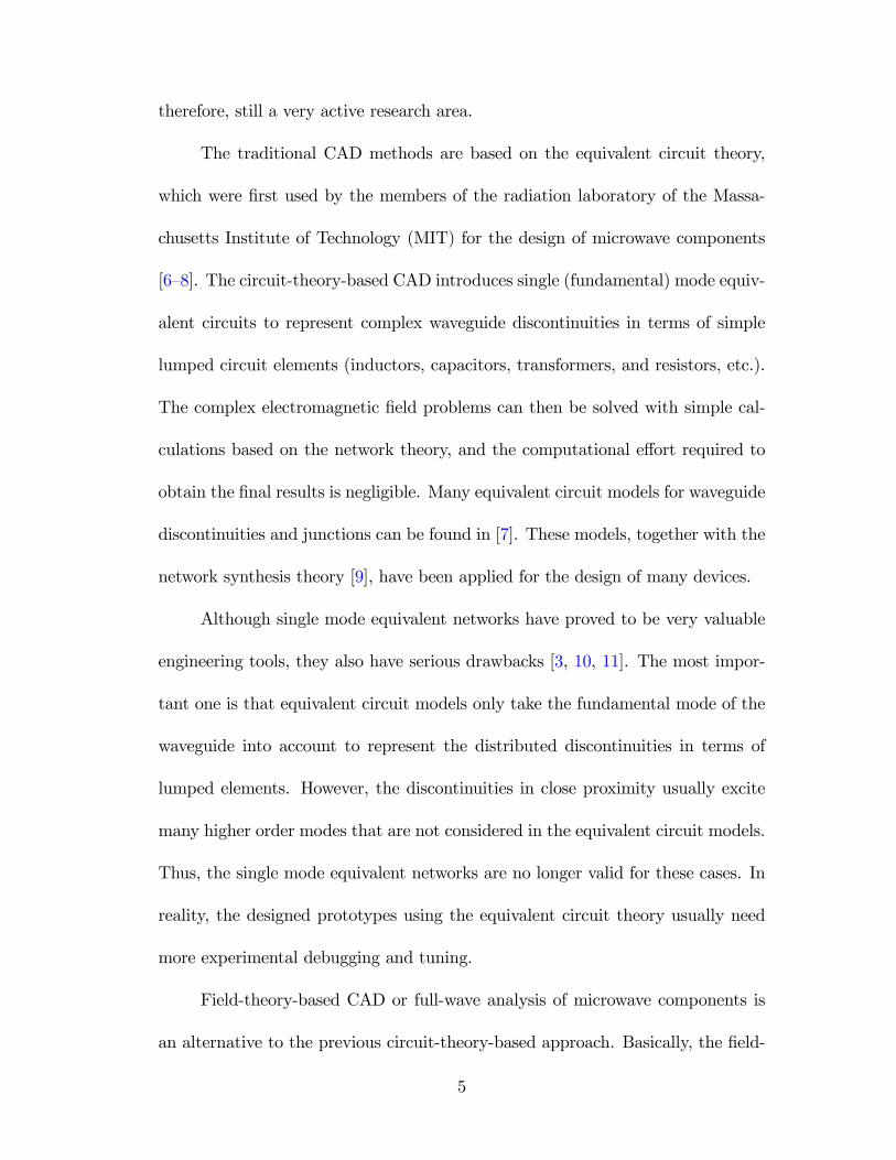
with a �eld-solver, hybrid approaches can be employed to improve the e¢ ciency.
One approach is to identify the key elements (discontinuities and junctions, etc.)
of the problem that need the �eld-solver, and to approximate the rest with the
equivalent circuit theory. An example is shown in Fig. 1.2 to demonstrate this
approach. The physical layout in Fig. 1.2(a) is a coupled-line bandpass �lter in
microstrip technology. This �lter structure has been subdivided using the library
of elements (transmission lines, mitered bends, and coupled-lines, etc.) in the
simulators for analysis. For the transmission lines, the physical dimensions are
6
(a)
(b)
(a)
(b)
Figure 1.2: (a) Physical layout of a coupled microstrip line �lter. (b) The layout of
(a) has been subdivided using the standard library elements for analysis.
related to impedance and electrical length through a set of closed form equations
(i.e. equivalent circuit model). For a discontinuity like the miter bend, a �eld-
solver can be used for the analysis to take the parasitic e¤ects into account. Shown
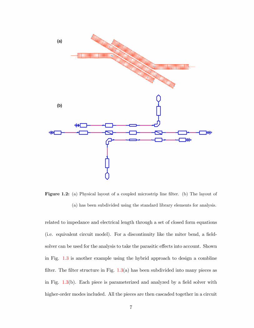
in Fig. 1.3 is another example using the hybrid approach to design a combline
�lter. The �lter structure in Fig. 1.3(a) has been subdivided into many pieces as
in Fig. 1.3(b). Each piece is parameterized and analyzed by a �eld solver with
higher-order modes included. All the pieces are then cascaded together in a circuit
7
(a)
(b)
(a)
(b)
Figure 1.3: (a) 3D structure of a combline �lter. (b) Subdivided circuits of (a) for
analysis. (reprinted from the archived seminar in Ansoft.com.)
simulator to obtain the frequency response. The tuning procedure is performed
in the circuit simulator to acquire the optimal design and improve the design ef-
�ciency. The development time can be signi�cantly reduced and the accuracy is
still remained. Another possible hybrid approach is to model a component using
a hybrid of two or more di¤erent numerical methods. The basic idea is to seg-
ment the component into di¤erent parts which are treated separately by di¤erent
numerical techniques [16]. Each part can be characterized by a multiple-mode
matrix, such as Generalized Scattering Matrix (GSM) and Generalized Admit-
tance Matrix (GAM). The response of the whole component can be obtained by
cascading all the part matrices together. For example, the �nite element method
(FEM) can be combined with mode matching method (MMM) to analyze and
design many waveguide components [17�19]. Some commercial CAD tools using
this hybrid approach are also available [20, 21].
8
1.2.2 General Numerical Methods
The purpose of all numerical methods in electromagnetics is to �nd approximate
solutions of Maxwell�s equations (or equations derived from them) that satisfy the
given boundary and initial conditions. Various numerical techniques are available,
and distinguished themselves from others mainly in three aspects [11]: i) The ap-
proximated electromagnetic quantity (electric �eld, magnetic �eld, potential, cur-
rent distribution, and charge distributions, etc.). ii) The expansion functions used
to approximate the unknown solutions. iii)The strategy (algorithms) employed to
determine the coe¢ cients of the expansion functions. The most representative
numerical methods [14] are:
� Finite Di¤erence Method [22]. This method can be categorized more as
Finite Di¤erence in Time Domain (FDTD) [23, 24] and Finite Di¤erence in
Frequency Domain (FDFD) [25]. Finite di¤erence method is well known to
be the least analytical.
� Finite Element Method (FEM) [26, 27]. FEM has variational features in
the algorithm that makes it di¤erent from the �nite di¤erence method. The
recently proposed Boundary Element Method (BEM) [28] is the combination
of the boundary integral equation and a discretization technique similar to
the FEM as applied to the boundary.
� Transmission Line Matrix method (TLM) [29, 30]. The �eld problem is
converted to a three dimensional equivalent network problem in this method.
9

� The Method of Moments (MoM) [15]. In the narrower sense, MoM is the
method of choice for solving problems stated in the form of an electric �eld
integral equation or a magnetic �eld integral equation.
� Mode Matching Method (MMM) [3, 10]. MMM is actually a �eld-matching
method that is usually used to obtain the GSMs or GAMs of waveguide
discontinuities (steps and junctions, etc.). The range of problems that can
be handled by MMM is constrained by the geometries and materials. Other
recently proposed advanced methods expanded from MMM are Boundary
Integral-Resonant Mode Expansion method (BIRME) [31, 32] and Boundary
Contour Mode Matching method (BCMM) [33�35]. These methods can be
employed to deal with the discontinuities with non-canonical shapes. MMM
is well known to be a very e¢ cient method.
� Spectral Domain Method (SDM) [36]. SDM is a Fourier-transformed version
of the integral equation method applied to planar structures. SDM is nu-
merically rather e¢ cient, but its range of applicability is generally restricted
to well-shaped structures.
A wide variety of commercial software tools based on the aforementioned
numerical techniques are available. Some of the well known software tools are
listed in Table 1.1. In reality, which numerical method (or commercial software)
to use usually depends on the geometry, accuracy, and e¢ ciency. For example,
if a component only involves canonical waveguide structures, MMM is usually
employed due to its high e¢ ciency and good accuracy. To analyze a multiple-layer
10
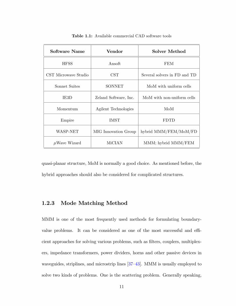
Table 1.1: Available commercial CAD software tools
Software Name Vendor Solver Method
HFSS Ansoft FEM
CST Microwave Studio CST Several solvers in FD and TD
Sonnet Suites SONNET MoM with uniform cells
IE3D Zeland Software, Inc. MoM with non-uniform cells
Momentum Agilent Technologies MoM
Empire IMST FDTD
WASP-NET MIG Innovation Group hybrid MMM/FEM/MoM/FD
�Wave Wizard MiCIAN MMM; hybrid MMM/FEM
quasi-planar structure, MoM is normally a good choice. As mentioned before, the
hybrid approaches should also be considered for complicated structures.
1.2.3 Mode Matching Method
MMM is one of the most frequently used methods for formulating boundary-
value problems. It can be considered as one of the most successful and e¢ -
cient approaches for solving various problems, such as �lters, couplers, multiplex-
ers, impedance transformers, power dividers, horns and other passive devices in
waveguides, striplines, and microstrip lines [37�43]. MMM is usually employed to
solve two kinds of problems. One is the scattering problem. Generally speaking,
11
when the geometry of the structure can be identi�ed as a junction (or discon-
tinuities) of two or more regions, MMM can then be used to solve the GSM,
GAM, or GIM (Generalized Impedance Matrix) characterization of the structure.
If a microwave component consists of a few junctions that are characterized by
GSMs solved in MMM, the scattering parameters of the component can easily be
obtained by cascading the GSMs together [14]. The other kind of problem that
can be handle by MMM is the eigenvalue problems. MMM can be formulated to
obtain the resonant frequency of a cavity, the cuto¤ frequencies of a waveguide,
or the propagation constant of a transmission line. The analysis in MMM of ce-
ramic cavities, generalized ridge waveguides, striplines, microstrip lines, and some
non-canonical waveguides as in Fig. 1.4 can be found in [35, 41, 44�46]. The mi-
crowave components presented in this dissertation are mostly designed in MMM.
Therefore, a brief introduction of MMM is given in this section.
To analyze a component or structure in MMM, three steps are usually fol-
lowed. The �rst step is to �nd the normal eigenmodes in each individual re-
gion (waveguide, coaxial line, stripline, and microstrip line, etc.) so that the
general electromagnetic �eld in each region can be expressed as a series of the
normal eigenmodes (with unknown coe¢ cients at this step). The normal eigen-
modes belong to one out of three groups: Transverse Electric (TE), Transverse
Magnetic (TM) or Transverse Electromagnetic (TEM) modes. The exact analyt-
ical solutions can be obtained for some canonical structures, such as rectangular
waveguides, circular waveguides, and coaxial waveguides [3, 7, 47, 48], while for
non-canonical structures as shown in Fig. 1.4, numerical methods are usually
12
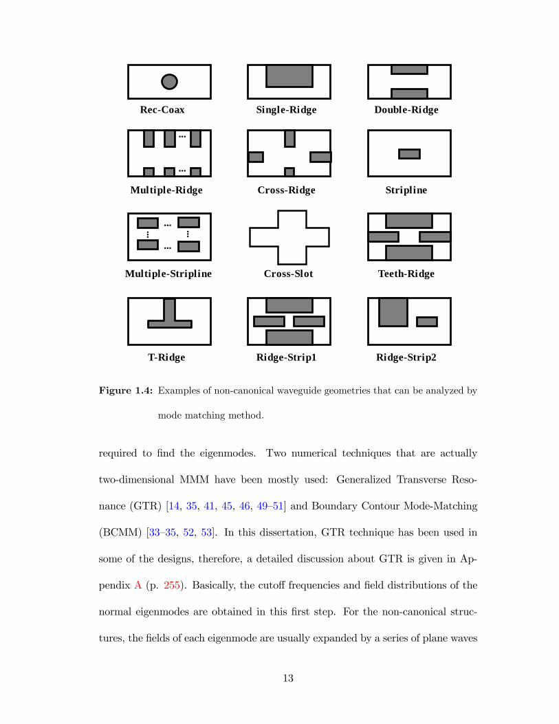
RecCoax SingleRidge DoubleRidge
...
...
MultipleRidge CrossRidge Stripline
MultipleStripline
...
......
...
CrossSlot TeethRidge
TRidge RidgeStrip1 RidgeStrip2
Figure 1.4: Examples of non-canonical waveguide geometries that can be analyzed by
mode matching method.
required to �nd the eigenmodes. Two numerical techniques that are actually
two-dimensional MMM have been mostly used: Generalized Transverse Reso-
nance (GTR) [14, 35, 41, 45, 46, 49�51] and Boundary Contour Mode-Matching
(BCMM) [33�35, 52, 53]. In this dissertation, GTR technique has been used in
some of the designs, therefore, a detailed discussion about GTR is given in Ap-
pendix A (p. 255). Basically, the cuto¤ frequencies and �eld distributions of the
normal eigenmodes are obtained in this �rst step. For the non-canonical struc-
tures, the �elds of each eigenmode are usually expanded by a series of plane waves
13

(L)
(s)
AL
As
z
(a) (b)
1 2
3
GAMa1
b1
b2
a2
a3 b3
GSMaL
bL
bs
as
(Z = 0)
(L)
(s)
AL
As
z
(L)
(s)
AL
As
z
(a) (b)
1 2
3
1 2
3
1 2
3
GAMa1
b1
b2
a2
a3 b3
GAMa1
b1
b2
a2
a3 b3
GSMaL
bL
bs
as
(Z = 0)
GSMaL
bL
bs
as
(Z = 0)
Figure 1.5: (a) A generic step discontinuity structure that can be characterized by
GSM. (b) A generic multiple-port junction structure that can be charac-
terized by GAM.
or circular waves with the solved coe¢ cients.
The second step is to characterize the junctions in one component by GSMs,
GAMs or GIMs based on the �eld-matching procedure. Basically, the �elds in
each individual region are described as the weighted sum of the normal eigen-
modes solved in the �rst step. The so-obtained �eld expansions are then matched
in the plane of the junction or discontinuity to derive the GSM or GAM. The
orthogonality property of the eigenmodes should be applied in this step. Two
kinds of junctions are usually treated by MMM. One is the step discontinuity
as shown in Fig. 1.5(a) that is characterized by GSM. The general formulations
to calculate the GSM are given in Table 1.2. The other kind of junction is the
14
generic multiple-port junction discontinuity as shown in Fig. 1.5(b) that is usu-
ally characterized by GAM. The basic procedure to calculate the GAM for such
a junction is to compute the magnetic �eld (corresponding to current) on the
ports when an electric �eld (corresponding to voltage) is excited in one of the
connection apertures. The ports except the excited port should be short-circuited
during this computation, which is consistent with the de�nition of the admittance
matrix. Once the �elds are known on each port, the elements of the GAM can
easily be obtained. The general GAM formulations can be found in [10, 35, 44],
and are not listed here. In general, the �nite number of normal eigenmodes is
used to approximate the �elds since it is not possible to extract an exact solution
with the in�nite number of eigenmodes. The accuracy of the approximated results
should be veri�ed carefully because of the relative convergence problem found in
the evaluation of the mode-matching equations [54].
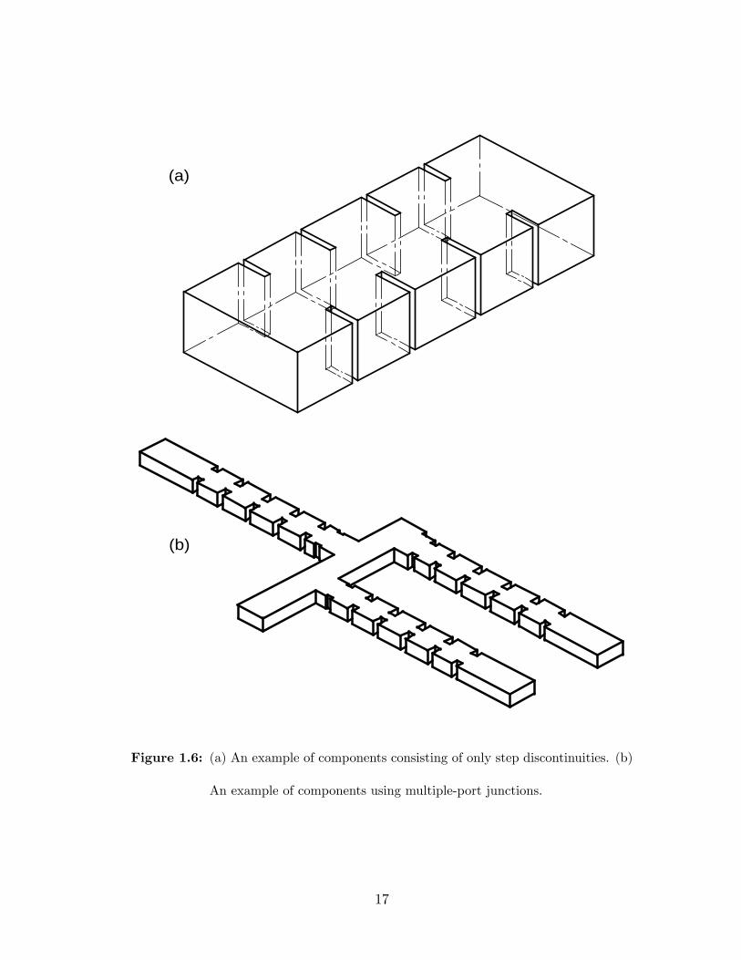
The third step of MMM is to obtain the scattering parameters of a compo-
nent by cascading the GSMs or GAMs of the junctions in the component together.
For instance, Shown in Fig. 1.6(a) is an H-plane inductive window �lter consisting
of only step discontinuities. The way to analyze it is just to characterize each step
as a GSM, and then perform the cascading. Fig. 1.6(b) is an H-plane manifold
triplexer. Two H-plane T-junctions are employed to ful�ll the manifold junction
and connect the three channel �lters. To analyze this component, the GAMs
for the T-junctions and the GSMs for the channel �lters are calculated �rst, and
then cascaded together to obtain the GSM of the whole triplexer. One necessary
procedure before cascading is to transform the GAMs or GIMs of multiple-port
15
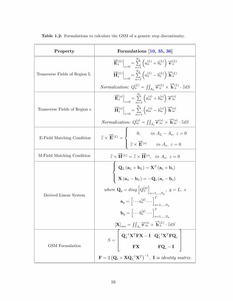
Table 1.2: Formulations to calculate the GSM of a generic step discontinuity.
Property Formulations [10, 35, 36]
Transverse Fields of Region L
�!E(L)t
���z=0=
NLPn=1
�a(L)n + b
(L)n
��!e (L)n
�!H(L)t
���z=0=
NLPn=1
�a(L)n � b(L)n
��!h(L)n
Normalization: Q(L)n =RRAL
�!e (L)n ��!h(L)n � bzdS
Transverse Fields of Region s
�!E(s)t
���z=0=
NsPm=1
�a(s)m + b
(s)m
��!e (s)m�!H(s)t
���z=0=
NsPm=1
�a(s)m � b(s)m
��!h(s)m
Normalization: Q(s)m =RRAs
�!e (s)m ��!h(s)m � bzdS
E-Field Matching Condition bz ��!E (L) =
8>><>>:0; in AL � As; z = 0
bz ��!E (s) in As; z = 0
M-Field Matching Condition bz ��!H(L) = bz ��!H(s); in As; z = 0
Derived Linear System
8>><>>:QL (aL + bL) = X
T (as + bs)
X (aL � bL) = �Qs (as � bs)
where Qg = diaghQ(g)n
in=1;:::;Ng
; g = L; s
ag =h� � � a(g)n � � �
iTn=1;:::;Ng
bg =h� � � b(g)n � � �
iTn=1;:::;Ng
[X]mn =RRAs
�!e (s)m ��!h(L)n � bzdS
GSM FormulationS =
2664 Q�1L X
TFX� I Q�1L X
TFQs
FX FQs � I
3775F = 2
�Qs +XQ
�1L X
T��1
; I is identity matrix.
16
(a)
(b)
(a)
(b)
Figure 1.6: (a) An example of components consisting of only step discontinuities. (b)
An example of components using multiple-port junctions.
17
junctions to equivalent GSMs. The relationship between the GSM, GAM and
GIM is given as the following equations [10, 35].
eY = eZ�1 = (I� S) (I+ S)�1eZ = eY�1 = (I+ S) (I� S)�1
S =�I+ eZ��1 �I� eZ� = �I� eY��I+ eY��1
(1.1)
where I is the identity matrix. eY and eZ are normalized or scaled versions of
the general GAM and GIM. The normalization or scale factors depend on the
relationship between the modal amplitudes and the voltages and currents [35]. It
must be pointed out that the phase delay of the connecting transmission structures
between the junctions must be taken into account for the cascading of GSMs.
Usually the number of modes used for the connections is much less than the
number of modes for the characterization of junctions since most of the modes are
evanescent in the connecting structures. To be complete, the resulting GSM SC
of cascading two GSMs SL and SR is given by [3, 35]
SC =
2664 SL11 + SL12WSR11S
L21 SL12WSR12
SR21�I+ SL22WSR11
�SL21 SR22 + S
R21S
L22WSR12
3775 (1.2)
where
W =�I� SR11SL22
��1; I is identity matrix.
1.3 Practical Realization Technologies
In practice, which technology to use for the realization of microwave passive com-
ponents, especially �lters and multiplexers, is related to many factors: frequency
18
range, quality factor Q, physical size, power handling capability, temperature
drifting, and cost, etc. A comprehensive consideration of these factors is usually
needed before choosing a realization technology for the desired components. Some
technologies are listed and discussed next.
1. Lumped-element �lters and multiplexers. The microwave frequency is
up to about 18 GHz. The unloaded Q averages about 200 (Q is dependent on
frequency), and over 800 may be achieved at lower frequencies [55]. The dimen-
sions are much smaller than distributed components, which is a major advantage.
The power handling capability is very low unless superconducting technology is
applied. The production cost is quite low. Lumped-element realizations of mi-
crowave components are not often used nowadays because the wavelength is so
short compared with the dimensions of circuit elements.
2. Vacuum- or Air-�lled Metallic-form components. Microwave components
implemented by vacuum- or air-�lled rectangular waveguides, ridge waveguides,
circular waveguides, and coaxial TEM lines belong to this category. The Q factors
can be realized from 5 to 20000 [9, 56, 57]. Waveguide �lters and multiplexers are
often employed for space and satellite applications to achieve high power handling
capability and high Q factor (silver-plated material can be used for higher Q).
The metallic-form components are usually bulky, and aluminum is mostly used
to have a light weight. The temperature stability of metallic-form components
usually needs to be improved for the space and satellite applications due to the
severe environment condition. The temperature drifting e¤ect can be compensated
or reduced by three ways: considerate design methodology, employing special
19
materials (e.g., Invar), and smart mechanical structures. Coaxial TEM �lters
and multiplexers are well-known for the low cost and the relatively high Q factor
(1 - 5000) [56, 58], and many standard components for wireless base station are
available in industries.
3. Planar structures. Microwave components realized by microstrip lines,
striplines, coplanar lines (waveguides), and suspended striplines belong to this
category. The main purpose of planar structures is to achieve the miniaturiza-
tion of the components. Planar structures are mostly employed for MICs and
MMICs. The power handling capability and Q factors are usually very low. Pla-
nar structures are the most �exible methods to implement �lters, and a variety of
structures have been and are being created by researchers.
4. Dielectric resonator �lters and multiplexers. Dielectric resonator �lters
and multiplexers are mostly employed to achieve very high Q and very good
temperature stability [57, 58]. The common designs use a cylindrical puck of
ceramic suspended on a supporter within a metallic housing. The fundamental
mode, hybrid modes, or multiple degenerate modes of the dielectric resonators can
be applied for the �lter designs. More than 50000 unloaded Q factor and less than
1 ppm/�C temperature coe¢ cient can be achieved by some ceramic materials.
5. Low Temperature Co-�red Ceramic (LTCC) technology. LTCC tech-
nology is commonly used for multiple-layer structures and packaging. Standard
LTCC technology is applied from few hundred MHz to about 40 GHz. The ad-
vantages of LTCC are cost e¢ ciency for high volumes, high packaging density,
reliability, and relatively higher Q than planar structures. Many waveguide com-
20
ponents have been manufactured by LTCC technology [59�64] to achieve a rela-
tively good Q factor. The unloaded Q factor is from 1 to 250 (depending on the
employed vendors). The basic way to realize waveguides in LTCC technology is
to use metallization and via fences to approximate the conductors and metallic
housing.
6. High temperature superconducting (HTS) components. In principle,
superconductivity enables resonators with near-in�nite unloaded Q to be con-
structed in a very small size. Examples can be found in [65, 66]. The disadvan-
tages of the HTS components are the bulky cooling system and the high power
consumption.
7. Surface acoustic wave (SAW) components. SAW devices operate by
manipulating acoustic waves propagating near the surface of piezoelectric crystals.
The frequency can be up to 3 GHz [57]. The main advantage of SAW components
is their very small size in applications such as cellular handsets. The Q factor,
power handling capability and temperature stability are usually poor. Examples
can be found in [67, 68].
8. Micromachined electromechanical systems (MEMS). MEMS-based prod-
ucts combine both mechanical and electronic devices on a monolithic microchip
to obtain superior performance over solid-state components, especially for wire-
less applications. The advantages of microwave-MEMS components are miniature
size, relatively low loss, and tunable property. MEMS technology are suitable for
handset �lters, transceiver duplexers, tunable resonators, switches, and tunable
�lters, etc. Micromechanical resonators with 7450 Q factor at 100 MHz have been
21
demonstrated in [69]. Examples of tunable �lters can be found in [70]. Tuning
bandwidths of up to 30% with Q of 300 are possible using MEMS technology [56].
1.4 Dissertation Objectives
This dissertation is devoted to creating innovated �lter and multiplexer structures
that will satisfy very stringent speci�cations, developing the precise modeling
and design procedures for microwave components, and integrating 3D component
structures for microwave integrated circuits.
With this general objective, the dissertation is mainly concentrating on �ve
di¤erent topics: i) Approximating, synthesizing and realizing generalized multiple-
band quasi-elliptic �lters. ii) Creating novel resonator structures to implement
miniature, ultra-wideband, and high performance �lters. iii) Inventing waveguide
structures to implement wideband �lters and multiplexers, and integrating them
in LTCC technology to achieve higher Q factors than planar structures. iv) Devel-
oping techniques to improve the spurious performance of the �lters. v) Creating
EM/Circuit combinational techniques for the �lter and multiplexer designs.
Many CAD tools have been used in this dissertation to perform the designs,
which include ad hoc mode-matching programs and some commercial software
tools in other numerical methods [71�73]. No matter which CAD tool has been
used, systematic modeling and design procedures have always been followed. A
systematic debugging and tuning procedure has also been created for quasi-elliptic
�lter designs.
22

LTCC technology has been employed to produce highly integrated microwave
circuits in this dissertation. Many multiple-layer and waveguide structures have
been designed and implemented for LTCC applications.
1.5 Text Organization
The dissertation is organized in �ve chapters, including this chapter for the intro-
duction. In chapter 2, the generalized approximation and synthesis methods of
multiple-band quasi-elliptic �lters are presented. An optimum equal-ripple perfor-
mance for a multiple-band quasi-elliptic �lter with any number of passbands and
stopbands can be obtained by the approximation procedure, which also allows the
use of real or complex transmission zeros in the �lter functions. For the synthesis
method, a powerful building-block cascading technique is developed to synthesize
various realizable network topologies.
Chapter 3 mainly concentrates on the microwave �lter designs. It begins
with the discussion of the generalized �lter design methodology that, actually,
can be applied to any �lter structures regardless of the geometry and implemen-
tation technology. In order to achieve miniaturization and wideband performance,
novel double-layer coupled stripline resonator �lter structures are developed. The
modeling and design of such �lters are performed in MMM and veri�ed by HFSS.
LTCC technology is employed to manufacture the �lters to gain the high inte-
gration. The measured results demonstrate a good agreement with the simulated
ones. The idea of double-layer resonator structures is then expanded to multiple-
23
layer coupled resonator structures. Two �lter designs using triple-layer coupled
stripline resonators and double-layer coupled hairpin resonators are performed in
Sonnet, respectively, to validate the concept. In order to obtain a good quality
factor with compact size, ridge waveguide coupled stripline resonator �lter struc-
tures, which can be in-line or folded, are created for LTCC applications. Analysis
and optimization in MMM are used to design such �lters. Stepped impedance
resonator (SIR) structure is also applied in the �lters to improve the spurious per-
formance. The dual-mode technology is applied for the realization of quasi-elliptic
�lters. A dual-mode circular waveguide �lter is designed and tuned on bench to
demonstrate the feasibility to realize an asymmetric �lter in dual-mode technol-
ogy, while a dual-mode rectangular waveguide �lter is modeled and designed in
MMM to show the realizability of having a dual-mode quasi-elliptic �lter without
any tuning screws. Finally, a systematic tuning procedure of quasi-elliptic �lters
is presented. A dielectric resonator �lter is tuned step by step to illustrate the
procedure.
Chapter 4 studies the modeling and design of microwave multiplexers. Gen-
eralized design methodologies are discussed at the beginning. Several multiplexer
designs are then performed for di¤erent perspectives. In order to obtain wideband
multiplexer designs in LTCC technology, ridge waveguide divider junctions are in-
vestigated and employed to realize multiplexers with the use of ridge waveguide
evanescent-mode �lters. Such structures can be highly integrated in LTCC tech-
nology and are appropriate for ultra-wideband multiplexer designs. The analysis
and optimization of such multiplexers are completely performed in MMM. Ku
24

band waveguide multiplexers for space applications are then presented. The mul-
tipaction discharge e¤ect on the power handling capability is discussed, and the
estimation method of multipaction threshold is explained. To avoid the tuning
of such multiplexers after the manufacture, round corners generated by the �nite
radius of the drill tool are included in the design step. A discretized step model
is employed in the analysis of MMM to represent the round corners. In order to
obtain miniaturized multiplexers with good quality factors, the stripline bifurca-
tion and T-junctions are used with the ridge waveguide coupled stripline resonator
�lters for multiplexer realizations. A diplexer design using stripline bifurcation
junction is performed in MMM to demonstrate the feasibility. Finally, a wide-
band waveguide diplexer is realized by waveguide E-plane bifurcation junction,
ridge waveguide evanescent-mode �lter, and iris coupled rectangular waveguide
�lter for high power application. The modeling and design of this diplexer are
performed in MMM and veri�ed by HFSS.
In chapter 5, conclusions of this dissertation are summarized, and the inter-
ested future research works are also addressed.
1.6 Dissertation Contributions
The main contributions of this dissertation are given as followings.
1. The generalized approximation procedure and the building-block synthesis
method are developed for multiple-band quasi-elliptic �lters. An optimum
equal-ripple performance in all passbands and stopbands is guaranteed.
25

2. Double-layer coupled stripline resonator �lter structures are created for
achieving the miniature and wideband performance. The modeling and de-
sign procedure of such �lters in MMM is developed.
3. Multiple-layer coupled resonator structures are proposed for miniature and
broadband �lter designs. The validity of the concept has been proved by
two �lter design examples.
4. Ridge waveguide coupled stripline resonator �lters and multiplexers are in-
vented to have a compact structure as well as a good quality factor. The
complete analysis and optimization procedure in MMM is developed.
5. Dual-mode �lter technology is applied for the realization of asymmetric �l-
ters. The feasibility is illustrated by a dual-mode circular waveguide �lter
prototype.
6. A dual-mode rectangular �lter structure is created for implementing quasi-
elliptic �lters without any tuning screws. The analysis and optimization are
carried out in MMM.
7. A systematic tuning procedure is proposed for quasi-elliptic �lters. The
procedure is generalized, and can be applied to any realization technology.
8. Ridge waveguide divider-type multiplexers are created to achieve high inte-
gration and ultra-wideband performance for LTCC applications. The mod-
eling and design are performed in MMM.
26

Chapter 2
Multiple-Band Quasi-Elliptic
Filters
2.1 Introduction
In recent years, with the development of concurrent multiple-band ampli�ers [74]
and multiple-band antennas [75], multiple-band �lters have been �nding applica-
tions in both space and terrestrial microwave telecommunication systems. The
system architecture is dramatically simpli�ed by using these multiple-band com-
ponents because non-contiguous channels can be transmitted to the same geo-
graphical region through only one beam [76]. Incorporating multiple passbands
within the single �lter structure o¤ers advantages over the equivalent multiplexing
solution, in terms of mass, volume, manufacturing, tuning and cost.
Three approaches are usually employed to implement multiple-band �lters.
The �rst approach is to use multiplexing method. Single-band bandpass �lters are
27

designed for each passband in a multiple-band �lter. Their input/output ports
are then connected together through junctions. This approach usually leads to a
complex design procedure since junctions and �lters have to be optimized to have
a good multiplexing performance and comply with the mechanical constraints.
The second approach is to use the multiple harmonic resonating modes of the
resonators [77, 78]. Each harmonic mode is employed to ful�ll one passband.
This approach has the di¢ culty to tune the harmonic modes to the desired center
frequencies of each passband. Therefore, it is often applied for dual-band �lter
designs. The third approach is to design a single circuit realizing the multiple-
band characteristics. This approach requires the approximation and synthesis of
an advanced �ltering function, but makes the hardware implementation easier
since the classical �lter architecture can be used.
This chapter discusses the approximation and synthesis methods for the
third approach. Some recent work on this subject has demonstrated the tech-
niques to synthesize dual-band �lters [79�81]. However, a generalized solution for
multiple-band �lters with real, imaginary or complex transmission zeros has not
been provided yet. In this chapter, an e¢ cient method based on iteration is pre-
sented for generating symmetric or asymmetric multiple-band transfer functions
with real, imaginary or complex transmission zeros.
A �lter design procedure commonly consists of three steps.
1. Solution to the approximation problem. A rational transfer function
needs to be found for multiple-band characteristics.
2. Solution to the synthesis problem. An equivalent lumped-element net-
28

work is synthesized to realize the transfer function.
3. Solution to the hardware implementation. Physical dimensions of a dis-
tributed �lter structure is obtained by full-wave numerical methods or tuning
methods based on the equivalent network.
Step 1 and 2 are detailedly presented in this chapter, while step 3 is only
brie�y discussed and more information can be found in later chapters.
2.2 The Approximation Problem
2.2.1 Problem Statement
The approximation problem for multiple-band �lters is mainly concerned with
obtaining realizable rational transfer functions of minimum degree with respect
to desired speci�cations, such as insertion loss, return loss, phase linearity, and
group delay, to produce the required amplitude response in all passbands and
stopbands, and the phase response in the passbands [82].
For any two-port lossless �lter network composed of a series of N coupled
resonators, the transfer and re�ection functions may be expressed as ratio of Nth
degree polynomials [83]
S11(s) =F (s)
E(s)and S21(s) =
P (s)
"E(s)(2.1)
where s is the complex frequency s = �+ j!, " is a constant scale factor to adjust
the equiripple levels. All the polynomials are monic. The polynomials F (s), P (s),
and E(s) must satisfy the following conditions to have a realizable lossless two
29

port network [57, 84]:
1. E(s) is a strict Hurwitz polynomial, i.e. all its roots must lie in the left
half s-plane.
2. The polynomial P (s) is of degree M � N � 1 and satis�es the condition
P = (�1)N+1P �, i.e. its roots must be symmetric with respect to the imaginary
axes.
3. F (s) is of degree N .
4. The conservation of energy for a lossless network generates the equation:
E(s)E�(s) = F (s)F �(s) +1
"2P (s)P �(s) (2.2)
Using (2.2), the transfer and re�ection functions can be expressed as
jS11(!)j2 ="2C2(!)
1 + "2C2(!)jS21(!)j2 =
1
1 + "2C2(!)(2.3)
where C(!) = F (!)P (!)
is know as the characteristic function. The approximation
problem is therefore simpli�ed to �nd the characteristic function C(s), and thus
the polynomials F (s), P (s) and E(s).
2.2.2 Determination of Characteristic Function C(s)
The determination of the characteristic function is based on the low-pass prototype
multiple-band �lters as shown in Fig. 2.1. A set of passbands and stopbands are
speci�ed by the normalized real frequency points. Each band is de�ned by two
frequency points except that the two outside stopbands are each speci�ed by one
point. The aim is to obtain an equiripple performance in each passband and
30
stopband, which will yield an optimum �ltering function mathematically. In Fig.
2.1, !0 is the right band-edge equiripple frequency point of the �rst stopband
(the left one is at negative in�nity). !1 and !2 are the two band-edge equiripple
frequency points for the �rst passband. !3 and !4 are the band-edge equiripple
frequency points for the second stopband. Similar speci�cations are given for other
�lter bands. It should be noted that the left (right) band-edge point of the most
left (right) passband is usually taken as �1 (+1) (!1 and !10 in Fig. 2.1) for the
normalization. Given the speci�ed passbands and stopbands, the requirements
are usually given on the minimum return loss (or maximum insertion loss) of the
passbands. The attenuation of the stopbands is normally controlled by the number
of transmission zeros. Other requirements, like phase and group delay, can also be
considered by using real or complex transmission zeros. According to the author�s
knowledge, there are no known analytical solutions to the approximation problem
of multiple-band �lters. A numerical method based on iteration is used to obtain
the optimum solution, which will be discussed next.
Roots of polynomials F (s) and P (s) are the poles and transmission zeros
of the multiple-band �ltering function. The characteristic function C(!) can be
represented as:
C(!) =F (!)
P (!)=
NYi=1
(! � pi)
MYj=1
(! � zj)(2.4)
where pi, i = 1; 2; :::; N , are poles of the passbands and must be real. zj, j =
1; 2; :::;M , are transmission zeros of stopbands and can be real, imaginary or
31
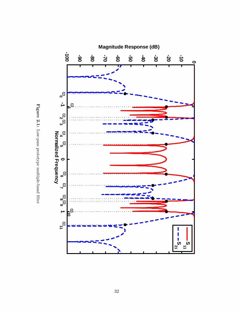
10
1100
90
80
70
60
50
40
30
20
10 0
Norm
alized Frequency
Magnitude Response (dB)S
11S
21
ω0
ω1
ω2 ω
3ω
4ω
5ω
6ω
7ω
8 ω9
ω10
ω11
Figu
re2.1:
Low-pass
prototypemultiple-band
�lter
32
complex. It must be noticed that pi and zj are now de�ned in the !-domain.
M � N � 1 must be satis�ed in order to have at least one transmission zero
at in�nity. By separating the real values of zj from the imaginary and complex
values, C(!) can be rewritten as:
C(!) =
NYi=1
(! � pi)
LYj=1
(! � rj)TYk=1
(! � ck)(2.5)
where rj, j = 1; 2; :::; L, are real values of z (imaginary transmission zeros in s-
domain). ck, k = 1; 2; :::; T , are imaginary or complex values of z (real or complex
transmission zeros in s-domain). ck must be given in conjugated pair. The total
number of transmission zeros M = L + T . Usually, real or complex transmis-
sion zeros are used to improve the phase linearity or the �atness of group delay.
Their values will be prescribed and �xed during the approximation procedure.
Therefore, the approximation problem can be re-phrased as:
Given the frequency range (band-edge equiripple points) of each passband
and stopband in a multiple-band �lter, the number of poles in each passband, the
number of imaginary zeros in each stopband, the prescribed real or complex zeros,
and the minimum return loss in each passband, the goal is to �nd the values of
poles ( pi in (2.5)) and imaginary zeros ( rj in (2.5)) for an optimum multiple-band
�ltering function, namely equiripple performance in each frequency band.
The procedure for �nding the equiripple response starts with the initial
guessing of a set of poles and zeros in every frequency band. The critical frequen-
cies, at which C(!) has its extrema, are then determined by solving for the roots
33
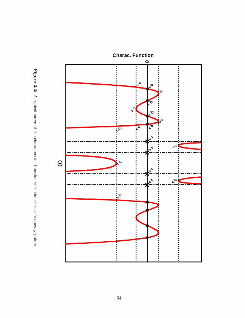
0
ω
Charac. Function
p1
p2
p3
p4
z1z2
z3z4
α0
α1
α2
α3
α4β0
β1
β2
β3
β4
Figu
re2.2:
Atypical
curveofthe
characteristicfunction
with
thecritical
frequencypoints
34
of the derivative of C(!):
dC(!)
d!= P (!)F
0(!)� F (!)P 0
(!) = 0 (2.6)
A typical curve of C(!) is shown in Fig. 2.2. Only three frequency bands,
two passbands and one stopband are displayed in the �gure. Other more frequency
bands in a multiple-band �lter are having the similar behaviors. Let the roots of
(2.6) in one passband be �1; �2:::; �K�1, where K is the number of poles in this
passband. Let �0 and �K represent the two band-edge equiripple points that are
given at the beginning. Therefore,
�0 < �1 < �2::: < �i::: < �K�1 < �K
Each pole of p�s in the passband should lie between two successive ��s as shown in
Fig. 2.2, i.e. �i�1 < pi < �i. With the �rst guessing of p�s, the absolute values of
C(!) at ��s usually are not equal (unless we are very lucky). Thus, new values of
p�s need to be found for an updated characteristic function, which will be closer
to an equiripple performance, according to the solved values of ��s. Let C0(!) be
the initial characteristic function and
C1(!) = (! � p0
l)
NYi=1;i6=l
(! � pi)
MYj=1
(! � zj)(2.7)
be the updated characteristic function with a new value p0l for the replacement of
the old value pl in C0(!). p0l is used to force C1(!) to have equal absolute values
at �l�1 and �l, that is
C1(�l�1) = �C1(�l) (2.8)
35

It must be pointed out that the index l for pl is a global index in all the
poles of the multiple-band �lter. It can be easily transformed into the local index
in the poles of a single passband. This transforming procedure has been ignored
for the sake of concision. From (2.7) and (2.8),
(�l�1 � p0
l)
NYi=1;i6=l
(�l�1 � pi)
MYj=1
(�l�1 � zj)= �(�l � p
0
l)
NYi=1;i6=l
(�l � pi)
MYj=1
(�l � zj)(2.9)
and
(�l�1 � p0l)
(�l�1 � pl)C0(�l�1) = �
(�l � p0l)
(�l � pl)C0(�l) (2.10)
After more manipulations, p0l is solved as
p0
l =pl [�l�1C0(�l�1) + �lC0(�l)]� �l�1�l [C0(�l�1) + C0(�l)]
pl [C0(�l�1) + C0(�l)]� [�lC0(�l�1) + �l�1C0(�l)](2.11)
For one stopband as in Fig. 2.2, let the roots of (2.6) in this stopband be
�1; �2:::; �I�1, where I is the number of zeros in this stopband. Let �0 and �I
represent the two band-edge equiripple points that are given at the beginning.
Each zero of z�s in the stopband should lie between two successive ��s as shown
in Fig. 2.2, i.e. �j�1 < zj < �j. Similar to the case of passband, the objective
is to �nd new values of z�s for an updated characteristic function to be closer
to an equiripple performance. The updated characteristic function C1(!) will be
expressed as
C1(!) =1
(! � z0l)
NYi=1
(! � pi)
MYj=1;j 6=l
(! � zj)(2.12)
36
where z0l is the new zero value for the replacement of the old value zl, such that
C1(�l�1) = �C1(�l) (2.13)
Thus,
1
(�l�1 � z0l)
NYi=1
(�l�1 � pi)
MYj=1;j 6=l
(�l�1 � zj)= � 1
(�l � z0l)
NYi=1
(�l � pi)
MYj=1;j 6=l
(�l � zj)(2.14)
which yields
z0
l =zl��l�1C0(�l) + �lC0(�l�1)
�� �l�1�l
�C0(�l�1) + C0(�l)
�zl�C0(�l�1) + C0(�l)
����l�1C0(�l�1) + �lC0(�l)
� (2.15)
One iteration to obtain an updated characteristic function is complete once
all the updated poles and zeros are found for each passband and stopband in a
multiple-band �lter. The roots of (2.6) using the updated characteristic function
are calculated again to check the values of C(!). The iteration will be continu-
ing until an equiripple performance with acceptable tolerance in every frequency
band is simultaneously achieved. The convergence of the iteration procedure is
guaranteed using the above updating method, and usually less than 20 iterations
is required.
2.2.3 Determination of E(s); F (s); and P (s)
After the poles and zeros are obtained by the iteration procedure, the polynomials
F (s) and P (s) are given as:
F (s) =NYi=1
(s� jpi); P (s) =MYk=1
(s� jzk) (2.16)
37
Equation (2.2) is then used to obtain the polynomial E(s). After some
derivations, the following expression is obtained.
Eleft(s)Eright(s) = F 2(s) + (�1)N�M P2(s)
"2(2.17)
where Eleft(s) is a polynomial with all its roots in the left half s-plane, which
is actually the wanted polynomial. Eright(s) has all its roots in the right half
s-plane. Value of " can be determined by the speci�ed minimum return loss in
the passbands. Therefore, the roots of the right-hand-side expression of (2.17) is
solved �rst. E(s) is then constructed by using the roots in the left half s-plane.
The unitary conditions on the scattering parameters are [2, 47]
S11S�11 + S21S
�21 = 1
S22S�22 + S12S
�12 = 1
S11S�12 + S21S
�22 = 0
(2.18)
According to (2.18), it may be shown that [47] the phases �, �1, and �2 of
S21(s), S11(s), and S22(s), respectively, are related by:
�� �1 + �22
=�
2(2k � 1); k is any integer (2.19)
Thus, to ensure the orthogonality between F (s) and P (s), P (s) given in
(2.16) should be updated as [85]:
P (s) =
8>><>>:P (s); if (N �M) is odd
j � P (s); if (N �M) is even(2.20)
After E(s), F (s), and P (s) are known, the transfer and re�ection functions
of a multiple-band �lter can be obtained straightforwardly.
38
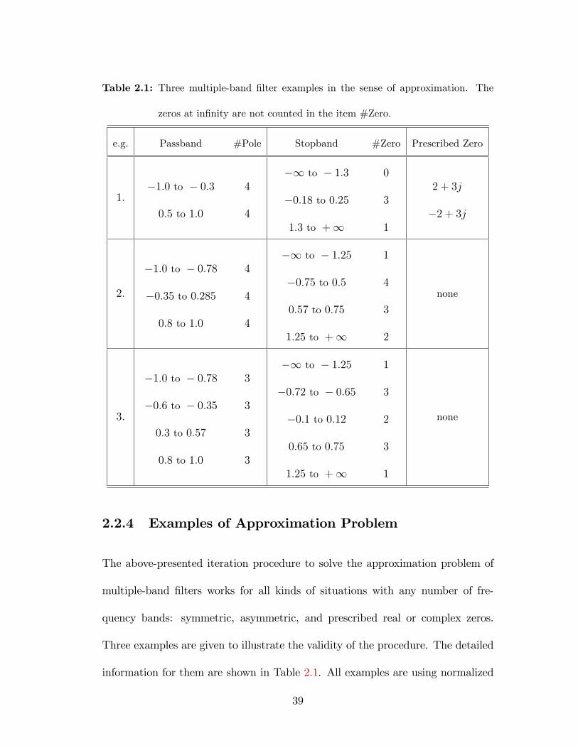
Table 2.1: Three multiple-band �lter examples in the sense of approximation. The
zeros at in�nity are not counted in the item #Zero.
e.g. Passband #Pole Stopband #Zero Prescribed Zero
1:�1:0 to � 0:3
0:5 to 1:0
4
4
�1 to � 1:3
�0:18 to 0:25
1:3 to +1
0
3
1
2 + 3j
�2 + 3j
2:
�1:0 to � 0:78
�0:35 to 0:285
0:8 to 1:0
4
4
4
�1 to � 1:25
�0:75 to 0:5
0:57 to 0:75
1:25 to +1
1
4
3
2
none
3:
�1:0 to � 0:78
�0:6 to � 0:35
0:3 to 0:57
0:8 to 1:0
3
3
3
3
�1 to � 1:25
�0:72 to � 0:65
�0:1 to 0:12
0:65 to 0:75
1:25 to +1
1
3
2
3
1
none
2.2.4 Examples of Approximation Problem
The above-presented iteration procedure to solve the approximation problem of
multiple-band �lters works for all kinds of situations with any number of fre-
quency bands: symmetric, asymmetric, and prescribed real or complex zeros.
Three examples are given to illustrate the validity of the procedure. The detailed
information for them are shown in Table 2.1. All examples are using normalized
39
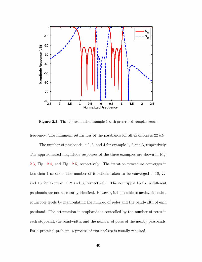
2.5 2 1.5 1 0.5 0 0.5 1 1.5 2 2.580
70
60
50
40
30
20
10
0
Normalized Frequency
Mag
nitu
de R
espo
nse
(dB
)
S11S
21
Figure 2.3: The approximation example 1 with prescribed complex zeros.
frequency. The minimum return loss of the passbands for all examples is 22 dB.
The number of passbands is 2, 3, and 4 for example 1, 2 and 3, respectively.
The approximated magnitude responses of the three examples are shown in Fig.
2.3, Fig. 2.4, and Fig. 2.5, respectively. The iteration procedure converges in
less than 1 second. The number of iterations taken to be converged is 16, 22,
and 15 for example 1, 2 and 3, respectively. The equiripple levels in di¤erent
passbands are not necessarily identical. However, it is possible to achieve identical
equiripple levels by manipulating the number of poles and the bandwidth of each
passband. The attenuation in stopbands is controlled by the number of zeros in
each stopband, the bandwidth, and the number of poles of the nearby passbands.
For a practical problem, a process of run-and-try is usually required.
40
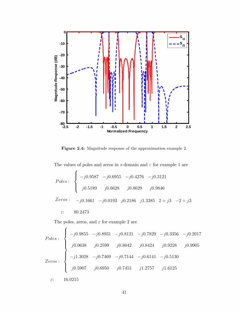
2.5 2 1.5 1 0.5 0 0.5 1 1.5 2 2.580
70
60
50
40
30
20
10
0
Normalized Frequency
Mag
nitu
de R
espo
nse
(dB
)
S11S21
Figure 2.4: Magnitude response of the approximation example 2.
The values of poles and zeros in s-domain and " for example 1 are
Poles :
8>><>>:�j0:9587 �j0:6955 �j0:4276 �j0:3121
j0:5189 j0:6628 j0:8629 j0:9846
Zeros : �j0:1661 �j0:0193 j0:2186 j1:3385 2 + j3 �2 + j3
": 80:2473
The poles, zeros, and " for example 2 are
Poles :
8>><>>:�j0:9855 �j0:8931 �j0:8121 �j0:7829 �j0:3356 �j0:2017
j0:0638 j0:2599 j0:8042 j0:8424 j0:9228 j0:9905
Zeros :
8>><>>:�j1:3028 �j0:7469 �j0:7144 �j0:6141 �j0:5130
j0:5907 j0:6950 j0:7451 j1:2757 j1:6125
": 16:0215
41
2 1.5 1 0.5 0 0.5 1 1.5 260
50
40
30
20
10
0
Normalized Frequency
Mag
nitu
de R
espo
nse
(dB)
S11S21
Figure 2.5: Magnitude response of the approximation example 3.
The poles, zeros, and " for example 3 are
Poles :
8>><>>:�j0:9811 �j0:8638 �j0:7875 �j0:5933 �j0:5172 �j0:3744
j0:3203 j0:4595 j0:5597 j0:8063 j0:8708 j0:9810
Zeros :
8>><>>:�j1:3062 �j0:7156 �j0:6841 �j0:6540 �j0:0673
j0:0940 j0:6568 j0:7043 j0:7451 j1:3110
": 4:0433
2.3 The Synthesis Problem
2.3.1 Problem Statement
Once the polynomials of the transfer and re�ection functions of a multiple-band
�lter are solved in the approximation problem, a lumped-element lossless network
42
needs to be synthesized to realize the desired �ltering function. Many synthesis
methods have been presented in published books and literature for single-band
�ltering functions. They are also applicable to multiple-band �lters since the
�ltering functions are constructed in the exactly same way mathematically (poly-
nomials are created based on the poles and zeros). Actually, two aspects can be
considered. One is that a single-band �lter is a special case of a multiple-band
�lter. The other one is that a multiple-band �lter is in fact a single-band �lter
with some transmission zeros inside the passband. The second aspect explains
why the synthesis methods for single-band �lters will also work for multiple-band
�lters.
The synthesis problem is to �nd the element values, namely coupling matrix,
of a lumped-element lossless network to realize the approximated �ltering func-
tion. The network topology should be simple enough to be realized by a classical
hardware implementation, for example, waveguide and planar structures. The
available synthesis methods can be separated into two categories. One is based
on the extraction procedure, which is usually a synthesis cycle to extract certain
elements one by one. For instance, the Darlington�s procedure [57, 84]. The other
category is based on the matrix and eigenvalue theory, which usually takes one
single step to yield all the elements of a generalized network. Once a generalized
network is obtained, more operations are usually performed on it to generate one
realizable network topology. This generalized network is therefore referred as a
starting network. The methods belonging to the second category are mostly used
nowadays, which will be discussed next.
43
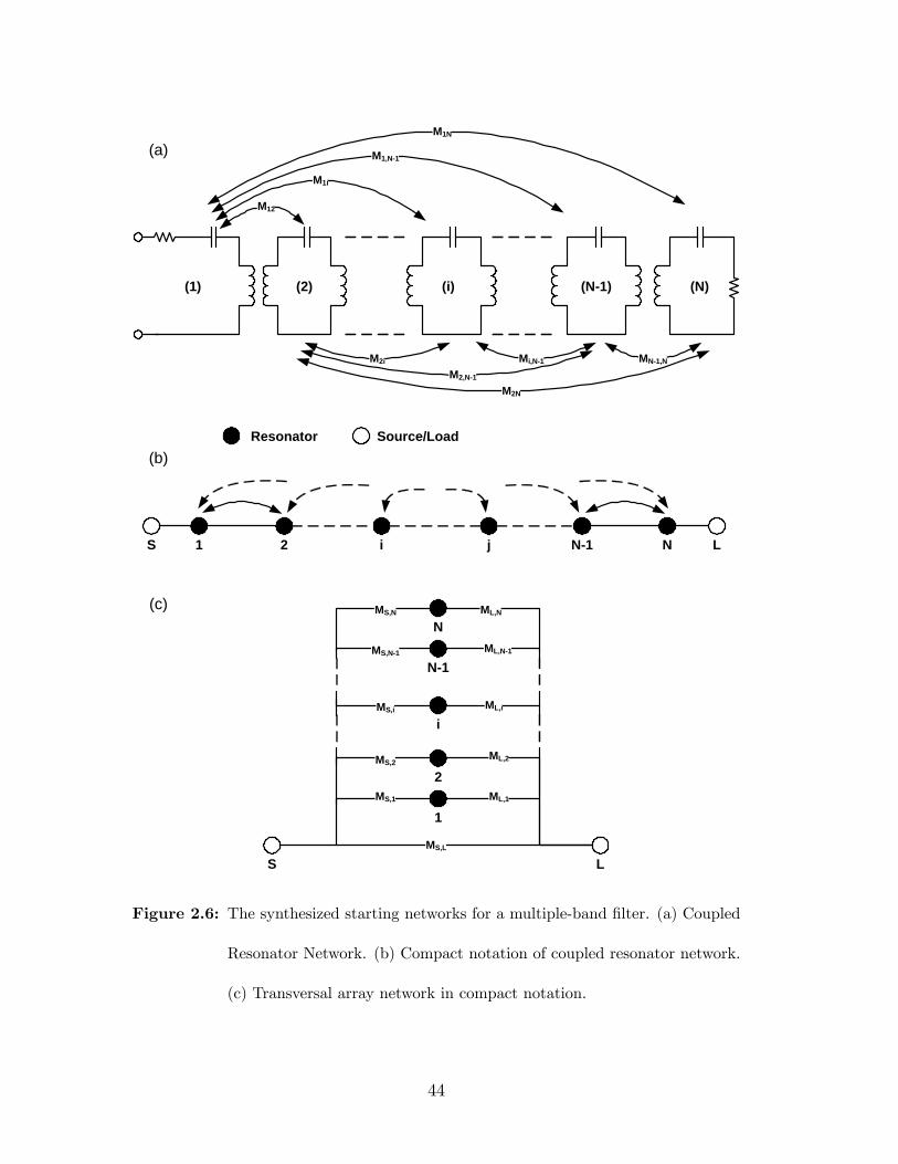
(1) (N)(N1)(i)(2)
M12
M1i
M1,N1
M1N
M2i Mi,N1 MN1,N
M2,N1
M2N
1 NN1jiS 2 L
S L
1
2
i
N1
N
MS,L
MS,1 ML,1
MS,2ML,2
MS,i ML,i
ML,N1MS,N1
MS,N ML,N
Resonator Source/Load
(a)
(b)
(c)
Figure 2.6: The synthesized starting networks for a multiple-band �lter. (a) Coupled
Resonator Network. (b) Compact notation of coupled resonator network.
(c) Transversal array network in compact notation.
44
2.3.2 Overview of Coupling Matrix Synthesis
One starting network �rstly presented by Atia et al [86] is the multiple coupled
resonator network as shown in Fig. 2.6(a) and (b). This network can have a
maximum of N � 2 �nite transmission zeros (assuming the �lter order is N) since
the source and load are each coupled to only one resonator. The other starting
network presented by Cameron [85] is the canonical transversal array network as
shown in Fig. 2.6(c). It has the advantage of being able to synthesize the fully
canonical �ltering functions (N poles with N transmission zeros) since multiple
source and load couplings are accommodated. The synthesis procedures of these
two networks have been clearly presented in [86] and [85]. The steps to obtain the
coupling matrix of each equivalent network are brie�y given in Table 2.2.
The coupling matrix topologies of the above two starting networks are too
complicated to be realized by hardware structures (one element is coupled to
many other elements). A similarity transformation (or rotation) procedure is
usually used to annihilate unwanted couplings and reduce the coupling matrix to
be a desired realizable topology. The use of similarity transforms ensures that
the eigenvalues and eigenvectors of the coupling matrix are preserved, such that
under analysis, the transformed matrix will yield exactly the same transfer and
re�ection characteristics as the original matrix [83, 85, 86]. LetM0 andM1 be the
original and transformed matrix, respectively, then the equation for a similarity
transform is given as:
M1 = R �M0 �Rt (2.21)
45
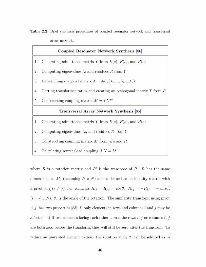
Table 2.2: Brief synthesis procedures of coupled resonator network and transversal
array network.
Coupled Resonator Network Synthesis [86]
1. Generating admittance matrix Y from E(s), F (s), and P (s)
2. Computing eigenvalues �i and residues R from Y
3. Determining diagonal matrix � = diag(�1; :::; �i; :::�n)
4. Getting transformer ratios and creating an orthogonal matrix T from R
5. Constructing coupling matrix M = T�T t
Transversal Array Network Synthesis [85]
1. Generating admittance matrix Y from E(s), F (s), and P (s)
2. Computing eigenvalues �i, and residues R from Y
3. Constructing coupling matrix M from �i�s and R
4. Calculating source/load coupling if N =M .
where R is a rotation matrix and Rt is the transpose of R. R has the same
dimensions as M0 (assuming N � N) and is de�ned as an identity matrix with
a pivot [i; j] (i 6= j), i.e. elements Ri;i = Rj;j = cos �r, Ri;j = �Rj;i = � sin �r,
(i; j 6= 1; N). �r is the angle of the rotation. The similarity transform using pivot
[i; j] has two properties [83]: i) only elements in rows and columns i and j may be
a¤ected. ii) If two elements facing each other across the rows i, j or columns i, j
are both zero before the transform, they will still be zero after the transform. To
reduce an unwanted element to zero, the rotation angle �r can be selected as in
46
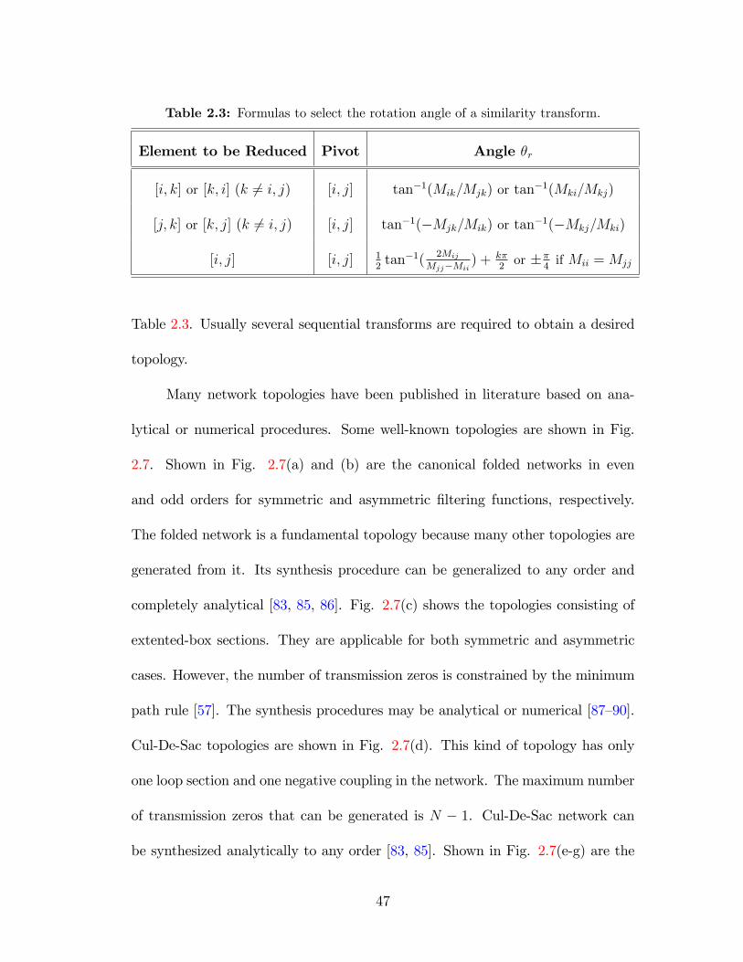
Table 2.3: Formulas to select the rotation angle of a similarity transform.
Element to be Reduced Pivot Angle �r
[i; k] or [k; i] (k 6= i; j) [i; j] tan�1(Mik=Mjk) or tan�1(Mki=Mkj)
[j; k] or [k; j] (k 6= i; j) [i; j] tan�1(�Mjk=Mik) or tan�1(�Mkj=Mki)
[i; j] [i; j] 12tan�1(
2Mij
Mjj�Mii) + k�
2or ��
4if Mii =Mjj
Table 2.3. Usually several sequential transforms are required to obtain a desired
topology.
Many network topologies have been published in literature based on ana-
lytical or numerical procedures. Some well-known topologies are shown in Fig.
2.7. Shown in Fig. 2.7(a) and (b) are the canonical folded networks in even
and odd orders for symmetric and asymmetric �ltering functions, respectively.
The folded network is a fundamental topology because many other topologies are
generated from it. Its synthesis procedure can be generalized to any order and
completely analytical [83, 85, 86]. Fig. 2.7(c) shows the topologies consisting of
extented-box sections. They are applicable for both symmetric and asymmetric
cases. However, the number of transmission zeros is constrained by the minimum
path rule [57]. The synthesis procedures may be analytical or numerical [87�90].
Cul-De-Sac topologies are shown in Fig. 2.7(d). This kind of topology has only
one loop section and one negative coupling in the network. The maximum number
of transmission zeros that can be generated is N � 1. Cul-De-Sac network can
be synthesized analytically to any order [83, 85]. Shown in Fig. 2.7(e-g) are the
47
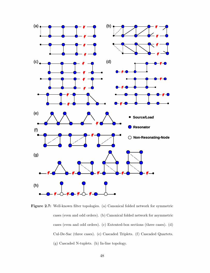
(a) (b)
(c) (d)
(e)
(f)
(g)
(h)
Source/Load
Resonator
NonResonatingNode
(a) (b)
(c) (d)
(e)
(f)
(g)
(h)
Source/Load
Resonator
NonResonatingNode
Figure 2.7: Well-known �lter topologies. (a) Canonical folded network for symmetric
cases (even and odd orders). (b) Canonical folded network for asymmetric
cases (even and odd orders). (c) Extented-box sections (three cases). (d)
Cul-De-Sac (three cases). (e) Cascaded Triplets. (f) Cascaded Quartets.
(g) Cascaded N-tuplets. (h) In-line topology.
48

topologies of cascaded triplets, cascaded quartets, and cascaded N -tuplets. Their
synthesis is based on the extraction of zeros and can be completely analytical
[91, 92]. One advantage of such networks is that the zero-generating locations can
be controlled through the synthesis procedure. An in-line topology using Non-
Resonating-Nodes (NRNs) is shown in Fig. 2.7(h). The elements are extracted
one by one according to the admittance matrix [93]. Many other discussions on
linear phase �lters and dual-band �lters are given in [79�81, 94, 95].
2.3.3 Cascaded Building-blocks
One important topology is the cascadedN -tuplet (CN) topology as in Fig. 2.7(g),
which consists of pure or mixed blocks of cascaded triplets (CT ), cascaded quar-
tets, and cascaded quintets, etc. Actually, the synthesis of CN topology is based
on the building block technique: a network is separated into two or more blocks
�rst, and then any transformation procedures can be applied on each block to obtain
a desired topology without a¤ecting other blocks. Basically, two steps are required:
i) Gathering N elements for a N -tuplet block. ii) Reducing the gathered N -tuplet
block to be a canonical folded topology or other topologies based on the well-
know rotation procedures. The reduction procedure at the second step will only
transform the N -tuplet block without a¤ecting other elements outside this block.
A pure CT network topology is appropriate for the building block technique
because it can be easily separated into blocks by simple rotations. Fig. 2.8 shows
one example to obtain a cascaded quintet block from the CT topology. Other N -
49
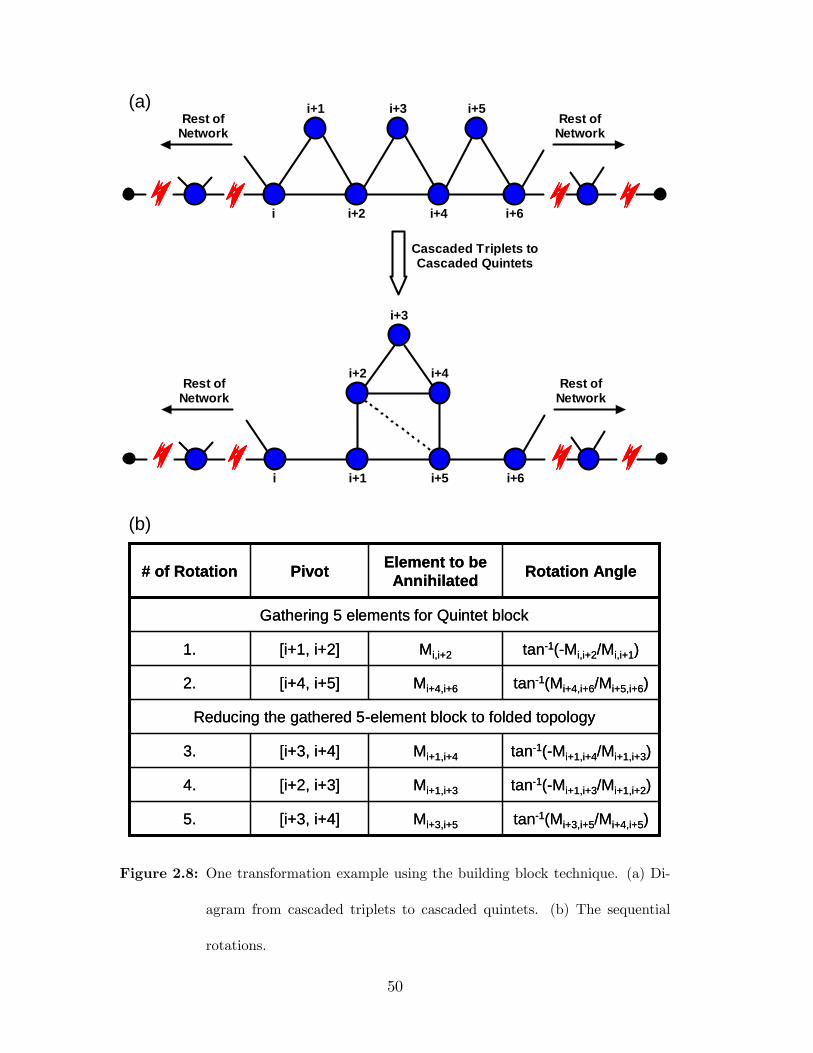
tan1(Mi+1,i+4/Mi+1,i+3)Mi+1,i+4[i+3, i+4]3.
tan1(Mi+1,i+3/Mi+1,i+2)Mi+1,i+3[i+2, i+3]4.
tan1(Mi+3,i+5/Mi+4,i+5)Mi+3,i+5[i+3, i+4]5.
Reducing the gathered 5element block to folded topology
tan1(Mi+4,i+6/Mi+5,i+6)Mi+4,i+6[i+4, i+5]2.
tan1(Mi,i+2/Mi,i+1)Mi,i+2[i+1, i+2]1.
Gathering 5 elements for Quintet block
Rotation AngleElement to beAnnihilatedPivot# of Rotation
i
i+1
i+2
i+3
i+4
i+5
i+6
Rest ofNetwork
Rest ofNetwork
i
i+2
i+1
i+3
i+5
i+4
i+6
Rest ofNetwork
Rest ofNetwork
Cascaded Triplets toCascaded Quintets
(a)
(b)
Figure 2.8: One transformation example using the building block technique. (a) Di-
agram from cascaded triplets to cascaded quintets. (b) The sequential
rotations.
50
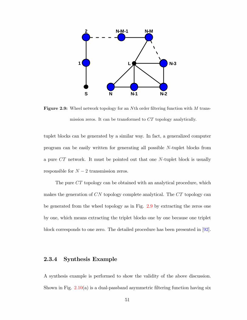
N
1
N1
NM
N2
N3
2
S
NM1
L
Figure 2.9: Wheel network topology for an Nth order �ltering function withM trans-
mission zeros. It can be transformed to CT topology analytically.
tuplet blocks can be generated by a similar way. In fact, a generalized computer
program can be easily written for generating all possible N -tuplet blocks from
a pure CT network. It must be pointed out that one N -tuplet block is usually
responsible for N � 2 transmission zeros.
The pure CT topology can be obtained with an analytical procedure, which
makes the generation of CN topology complete analytical. The CT topology can
be generated from the wheel topology as in Fig. 2.9 by extracting the zeros one
by one, which means extracting the triplet blocks one by one because one triplet
block corresponds to one zero. The detailed procedure has been presented in [92].
2.3.4 Synthesis Example
A synthesis example is performed to show the validity of the above discussion.
Shown in Fig. 2.10(a) is a dual-passband asymmetric �ltering function having six
51

poles and three transmission zeros. Its dual passbands are: [�1 to �0:3] and [0:42
to 1]. Its stopbands are: [�0:11 to 0:1] and [1:4 to +1]. Four possible network
topologies as shown in Fig. 2.10(b) have been synthesized to realize the �ltering
function, namely folded topology, Cul-De-Sac topology, Cascaded triplets topol-
ogy, and Cascaded Quartet-Triplet topology. The synthesized coupling matrix for
each topology is given as the followings.
1. Non-zero elements in the coupling matrix of the folded network are:
MS1 = 0:8999; M11 = 0:0843; M12 = 0:8793; M22 = 0:0365; M23 = 0:3674;
M25 = 0:3777; M26 = 0:3313; M33 = �0:0654; M34 = 0:3423; M35 = �0:0810;
M44 = �0:1853; M45 = 0:3907; M55 = �0:2708; M56 = 0:8145; M66 = 0:0843;
M6L = 0:8999.
2. Non-zero elements in the coupling matrix of the Cul-De-Sac topology
are: MS1 = 0:8999; M11 = 0:0843; M12 = 0:7296; M15 = �0:4909; M22 = 0:2905;
M23 = 0:3391; M26 = 0:7296; M33 = 0:2222; M44 = �0:4729; M45 = 0:4234;
M55 = �0:5249; M56 = 0:4909; M66 = 0:0843; M6L = 0:8999.
3. Non-zero elements in the coupling matrix of the CT network are: MS1 =
0:8999; M11 = 0:0843; M12 = 0:4460; M13 = 0:7578; M22 = �0:0336; M23 =
�0:2039; M33 = 0:3007; M34 = �0:2729; M35 = 0:6052; M44 = �0:2098; M45 =
0:3210; M55 = 0:4604; M56 = 0:4547; M5L = 0:5716; M66 = �0:9183; M6L =
0:6950.
4. Non-zero elements in the coupling matrix of the CQ-CT topology are:
MS1 = 0:8999; M11 = 0:0843; M12 = 0:5701; M14 = 0:6695; M22 = �0:0639;
M23 = 0:0574; M24 = 0:0861; M33 = 0:1585; M34 = 0:3972; M44 = �0:0374;
52
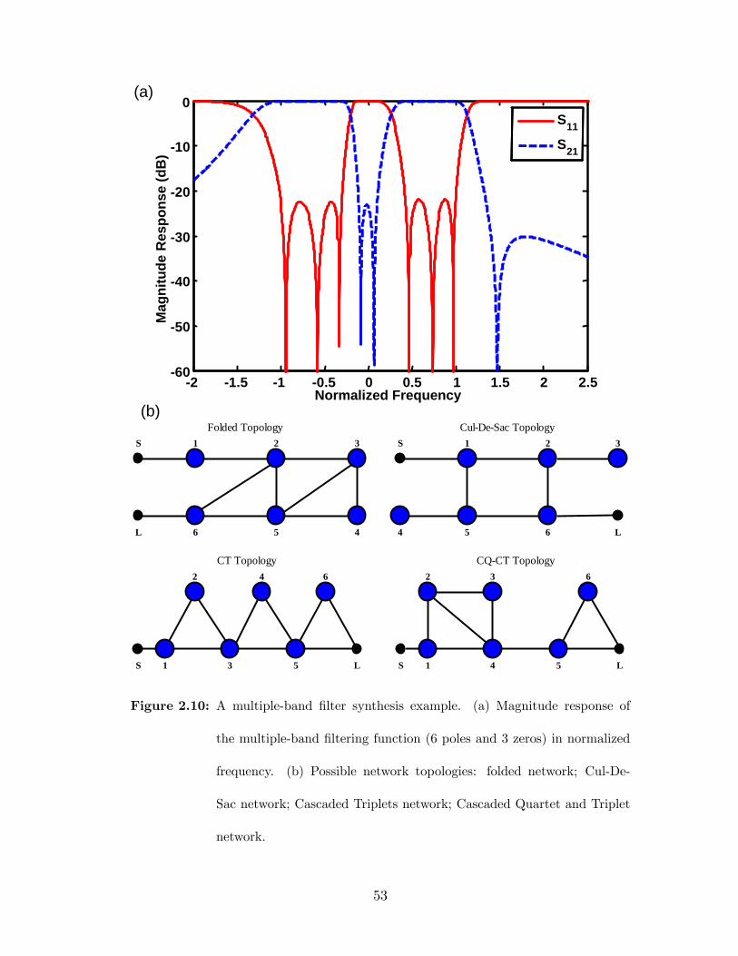
2 1.5 1 0.5 0 0.5 1 1.5 2 2.560
50
40
30
20
10
0
Normalized Frequency
Mag
nitu
de R
espo
nse
(dB
)
S11
S21
2 1.5 1 0.5 0 0.5 1 1.5 2 2.560
50
40
30
20
10
0
Normalized Frequency
Mag
nitu
de R
espo
nse
(dB
)
S11
S21
S 1 2 3
L 6 5 4
S 1 2 3
L5 64
Folded Topology CulDeSac Topology
L
2 4 6
S 1 3 5
CT Topology
L
2 3 6
S 1 4 5
CQCT Topology
(a)
(b)
Figure 2.10: A multiple-band �lter synthesis example. (a) Magnitude response of
the multiple-band �ltering function (6 poles and 3 zeros) in normalized
frequency. (b) Possible network topologies: folded network; Cul-De-
Sac network; Cascaded Triplets network; Cascaded Quartet and Triplet
network.
53
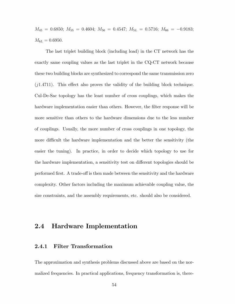
M45 = 0:6850; M55 = 0:4604; M56 = 0:4547; M5L = 0:5716; M66 = �0:9183;
M6L = 0:6950.
The last triplet building block (including load) in the CT network has the
exactly same coupling values as the last triplet in the CQ-CT network because
these two building blocks are synthesized to correspond the same transmission zero
(j1:4711). This e¤ect also proves the validity of the building block technique.
Cul-De-Sac topology has the least number of cross couplings, which makes the
hardware implementation easier than others. However, the �lter response will be
more sensitive than others to the hardware dimensions due to the less number
of couplings. Usually, the more number of cross couplings in one topology, the
more di¢ cult the hardware implementation and the better the sensitivity (the
easier the tuning). In practice, in order to decide which topology to use for
the hardware implementation, a sensitivity test on di¤erent topologies should be
performed �rst. A trade-o¤ is then made between the sensitivity and the hardware
complexity. Other factors including the maximum achievable coupling value, the
size constraints, and the assembly requirements, etc. should also be considered.
2.4 Hardware Implementation
2.4.1 Filter Transformation
The approximation and synthesis problems discussed above are based on the nor-
malized frequencies. In practical applications, frequency transformation is, there-
54
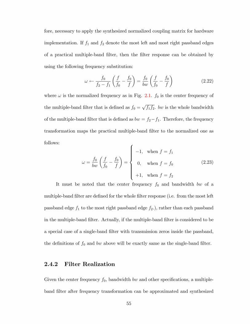
fore, necessary to apply the synthesized normalized coupling matrix for hardware
implementation. If f1 and f2 denote the most left and most right passband edges
of a practical multiple-band �lter, then the �lter response can be obtained by
using the following frequency substitution:
! f0f2 � f1
�f
f0� f0f
�=f0bw
�f
f0� f0f
�(2.22)
where ! is the normalized frequency as in Fig. 2.1. f0 is the center frequency of
the multiple-band �lter that is de�ned as f0 =pf1f2. bw is the whole bandwidth
of the multiple-band �lter that is de�ned as bw = f2�f1. Therefore, the frequency
transformation maps the practical multiple-band �lter to the normalized one as
follows:
! =f0bw
�f
f0� f0f
�=
8>>>>>><>>>>>>:�1; when f = f1
0; when f = f0
+1; when f = f2
(2.23)
It must be noted that the center frequency f0 and bandwidth bw of a
multiple-band �lter are de�ned for the whole �lter response (i.e. from the most left
passband edge f1 to the most right passband edge f2.), rather than each passband
in the multiple-band �lter. Actually, if the multiple-band �lter is considered to be
a special case of a single-band �lter with transmission zeros inside the passband,
the de�nitions of f0 and bw above will be exactly same as the single-band �lter.
2.4.2 Filter Realization
Given the center frequency f0, bandwidth bw and other speci�cations, a multiple-
band �lter after frequency transformation can be approximated and synthesized
55
through the afore-presented procedures, and a normalized coupling matrix for
a desired topology can be obtained. The normalized coupling matrix must be
transformed to the actual coupling values for �lter realization as follows:8>><>>:Mij � bw; in frequency unit
Mij � bwf0 ; in normal unit
(2.24)
During the �lter realization, the center frequency f0 and the actual coupling
values of the multiple-band �lter are mapped to the physical structures and dimen-
sions by appropriate CAD tools. Tuning and optimization are usually required
to obtain the desired �lter performance. Actually, the realization methodology of
multiple-band �lters is completely identical with single-band �lters. The detailed
information about �lter realization can be found in Chapter 3.
56
Chapter 3
Microwave Filter Designs
3.1 Design Methodology
3.1.1 Introduction
Microwave �lters belong to the most commonly used passive components in any
microwave system. They are, by nature, distributed networks that usually consist
of periodic structures to exhibit passband and stopband characteristics in various
frequency bands. It is desirable that a design method would be able to determine
the physical dimensions of a �lter structure having the desired frequency charac-
teristics. Research on microwave �lters has spanned more than sixty years, and
the number of contributions devoted to the design methods of microwave �lters
is enormous. Reviews on the topic of �lter designs in a historical perspective can
be found in [9, 55, 56].
In the following subsection, a generalized design method for a wide variety of
57
microwave and millimeter-wave �lters will be presented. The method depends on
a combination of a simple synthesis and an accurate analysis based on advanced
numerical methods. Basically, the �lter designs proceed from the synthesis of
the lumped-element low-pass prototypes. The physical dimensions/parameters of
�lter structures are then related to the corresponding parameters of the prototypes
by numerical analysis. Optimization and tuning procedures are usually involved in
microwave �lter designs. For most of the �lter designs, �eld-theory-based analysis
is an integrated part of the design process. Such analysis methods allow �lter
responses to be predicted very accurately, so that the experimental adjustments
of the manufactured components can be reduced or eliminated. For some �lter
structures that can not be e¢ ciently optimized by numerical methods due to the
structure complexity or the lengthy simulation speed, experimental tuning is a
necessary step in the design procedure. The tuning process can be guided by
computer programs according to the parameter extraction methods.
The analysis of �lter structures in this dissertation is mostly addressed with
the mode matching method (MMM). MMM has the advantage of high e¢ ciency,
which makes it the most preferable for the full-wave analysis and optimization
procedure. However, MMM is a structure-related method, which means that
knowledge of di¤erent structures needs to be studied individually in order to create
ad hoc MMM codes to perform the rigorous full-wave analysis on them. Other
numerical methods, such as FEM and MoM, provided by the commercial software
tools [71�73] are also employed in this dissertation to analyze some structures that
can not be tackled by MMM and verify the �nal designs performed in MMM. In
58

addition, the post-processing features, like �eld calculations and plots, in these
commercial software tools are also used to gain an insight into the component
operation.
3.1.2 Generalized Design Approach
A generalized design procedure shown in Fig. 3.1 as a �ow chart has been followed
in this dissertation to perform the �lter designs. The detailed concerns on each
step will be discussed in the following points.
1. The design procedure begins with the desired �lter performance. The
performance is usually determined by the requirement of a microwave system and
expressed in terms of electrical, mechanical, and environmental parameters. Com-
monly used electrical parameters are: center frequency, bandwidth, insertion loss,
gain �atness, return loss, stopband attenuation, group delay or phase linearity,
and power handling capability, etc. Mechanical requirements are usually char-
acterized by constraints of the maximum volume, weight, and �lter interfaces.
Environmental requirements include the vibration test and the thermal drifting
limitation (i.e., the electrical performance must be maintained in the considered
environments). Even though the objective of a design is to satisfy all the given
speci�cations, sometimes a compromise has to be made between the electrical,
mechanical and environmental requirements to obtain a feasible physical struc-
ture. Therefore, �nal speci�cations of a �lter design are usually decided with the
consideration of the system requirements, the physical realizability, the design
59
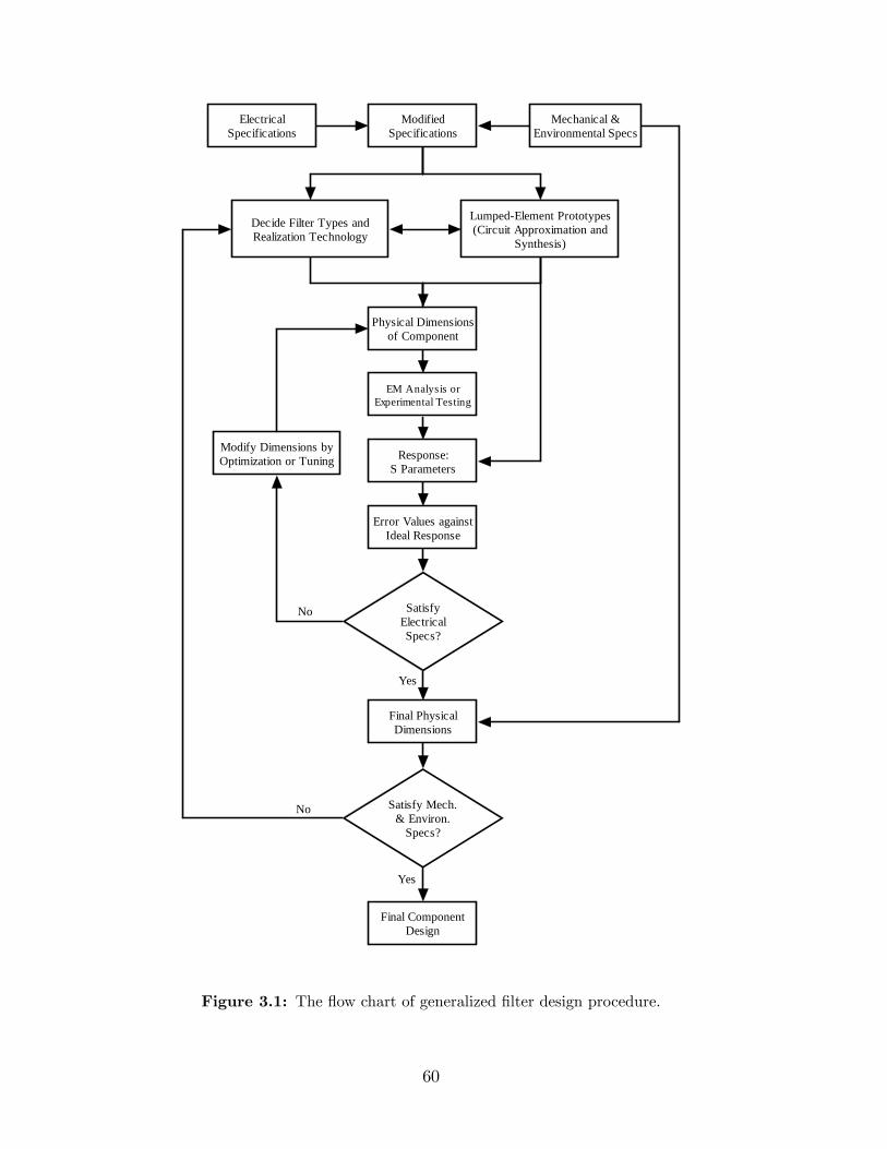
ModifiedSpecifications
ElectricalSpecifications
Mechanical &Environmental Specs
LumpedElement Prototypes(Circuit Approximation and
Synthesis)
Decide Filter Types andRealization Technology
Physical Dimensionsof Component
EM Analysis orExperimental Testing
Response:S Parameters
Error Values againstIdeal Response
Modify Dimensions byOptimization or Tuning
Final PhysicalDimensions
Satisfy Mech.& Environ.
Specs?
SatisfyElectricalSpecs?
Final ComponentDesign
Yes
Yes
No
No
Figure 3.1: The �ow chart of generalized �lter design procedure.
60
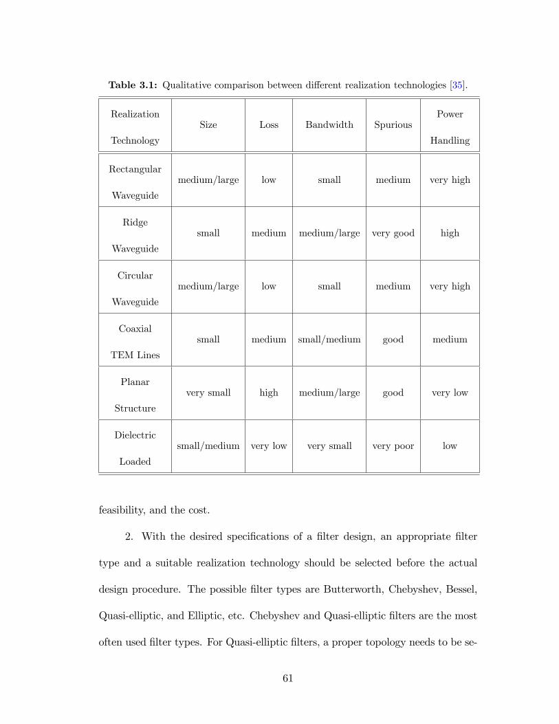
Table 3.1: Qualitative comparison between di¤erent realization technologies [35].
Realization
Technology
Size Loss Bandwidth SpuriousPower
Handling
Rectangular
Waveguide
medium/large low small medium very high
Ridge
Waveguide
small medium medium/large very good high
Circular
Waveguide
medium/large low small medium very high
Coaxial
TEM Lines
small medium small/medium good medium
Planar
Structure
very small high medium/large good very low
Dielectric
Loaded
small/medium very low very small very poor low
feasibility, and the cost.
2. With the desired speci�cations of a �lter design, an appropriate �lter
type and a suitable realization technology should be selected before the actual
design procedure. The possible �lter types are Butterworth, Chebyshev, Bessel,
Quasi-elliptic, and Elliptic, etc. Chebyshev and Quasi-elliptic �lters are the most
often used �lter types. For Quasi-elliptic �lters, a proper topology needs to be se-
61
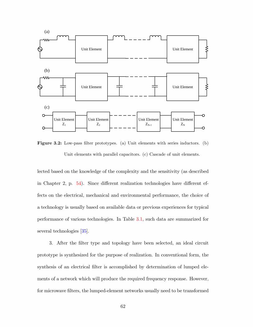
Unit ElementUnit Element
Unit ElementZ1
Unit ElementZ2
Unit ElementZN1
Unit ElementZN
Unit ElementUnit Element
(a)
(b)
(c)
Figure 3.2: Low-pass �lter prototypes. (a) Unit elements with series inductors. (b)
Unit elements with parallel capacitors. (c) Cascade of unit elements.
lected based on the knowledge of the complexity and the sensitivity (as described
in Chapter 2, p. 54). Since di¤erent realization technologies have di¤erent ef-
fects on the electrical, mechanical and environmental performance, the choice of
a technology is usually based on available data or previous experiences for typical
performance of various technologies. In Table 3.1, such data are summarized for
several technologies [35].
3. After the �lter type and topology have been selected, an ideal circuit
prototype is synthesized for the purpose of realization. In conventional form, the
synthesis of an electrical �lter is accomplished by determination of lumped ele-
ments of a network which will produce the required frequency response. However,
for microwave �lters, the lumped-element networks usually need to be transformed
62

to an appropriate format that would lead to the physical dimensions of the device.
The commonly used networks for low-pass and bandpass �lters are discussed next.
The prototypes for highpass and bandstop �lters can also be obtained by using
the well-known transformations from low-pass prototypes.
� One ideal prototype for low-pass �lter is using the unit elements with series
inductors or parallel capacitors as shown in Fig. 3.2(a) and (b), where a
unit element is a lossless transmission line of unit length, for example quar-
ter wavelength. Kuroda�s identities are usually used for the transformation
of this prototype network [2]. Detailed information about the transforma-
tion procedure can be found in [96]. Another ideal prototype for low-pass
�lter is the stepped impedance unit element network as in Fig. 3.2(c). This
prototype consists entirely of a cascade of unit elements with di¤erent char-
acteristic impedances. The detailed synthesis theory on this prototype has
been given in [82, 97, 98]. Other ideal prototypes for low-pass �lter can be
found in [57].
� One ideal prototype for bandpass �lter is the multiple coupled resonator
network discussed in chapter 2. The values of mutual couplings (impedance
inverters or admittance inverters) and self couplings need to be found for a
selected network topology by using the synthesis methods given in chapter
2. Some other prototypes for extracted-pole �lters and linear phase �lters
can be found in [99�101].
4. The initial dimensions of the physical �lter structure are found according
63
to the synthesized circuit prototypes and the selected realization technology. The
response of the initial �lter structure should be close to the ideal response of the
equivalent circuit. The initial dimensions are commonly generated by mapping
the physical dimensions with the elements of the synthesized equivalent circuit.
The possible mapping methods are given as below.
� Commensurate network transformations are usually used for low-pass �lter
realizations. Unit elements are implemented as transmission lines with the
required electrical length and characteristic impedance. Inductors and ca-
pacitors are transformed into short-circuited or open-circuited stubs using
Richard�s transformation [2, 57]. This method is commonly applied to TEM
transmission line low-pass �lters, however, it can also be used on pseudo-
low-pass �lter designs with waveguide structures, such applications can be
found in [102�104].
� Classical formulas approximating electromagnetic modes are used to re-
late the waveguide dimensions (especially junctions) to the circuit elements,
which can be found in [7]. Other circuit models taking into account some
higher order modes for the discontinuities are presented in [105�107], which
is more accurate than the formulas.
� Full-wave numerical techniques are employed to analyze the cavity, disconti-
nuity, and part region in a �lter structure, so that the equivalent circuit pa-
rameters can be generated to model these structures. All the aforementioned
numerical methods can be used for the analysis, however, the e¢ ciency, the
64
capability, and the accuracy should be considered to select an appropriate
method. Basically, numerical methods are used to determine the resonant
frequency of the cavity, the inter-coupling values between two cavities, and
the external coupling of input/output interface [45, 108�111]. Usually, a
curve or table relating the determined values to the physical dimensions can
be obtained. The initial physical dimensions are then determined by inter-
polation method based on the synthesized circuit prototype. The response
of the initial �lter structure is mostly very close to the desired one due to
the precise analysis of the full-wave numerical methods.
5. Optimization or tuning of the complete component is performed to im-
prove the �lter performance once the initial dimensions of the �lter structure have
been obtained. if a �lter structure can be rigorously and e¢ ciently analyzed by
full-wave numerical techniques, a full-wave optimization procedure is usually ap-
plied to �nd the optimum dimensions that will generate the desired response.
Some common optimization algorithms are: Quasi-Newton, Simplex, Random
walk, Simulated Annealing and Gradient Technique. The detailed information
regarding the features of each algorithm can be found in [35, 112�114]. Optimiza-
tion routines usually need to minimize an error function. A typical error function
is expressed as
err(x) =
NpXi=1
wp fdB [S11(x; fp;i)] + rg2 +NIsX
i=1
wIs�dB�S21(x; f
Is;i)�+ aI
2+
NIIsXi=1
wIIs�dB�S21(x; f
IIs;i)�+ aII
2(3.1)
65
where Np, N Is , and N
IIs are the number of frequency points in the passband, stop-
band I (lower), and stopband II (higher), respectively. f�s represent the sampled
frequency points in passband and stopband. x is the geometrical parameters of the
�lter to be optimized. w�s are the weight factors for controlling the contributions
of each error element. Operator dB(�) is to transform S-parameters in unit of dB.
r, aI , and aII are the desired return loss, attenuation in stopband I, and atten-
uation in stopband II, respectively. In practical design, the optimization should
go gradually to achieve the ultimate goal, which means that some intermediate
less-aggressive goals should be ful�lled by the optimizer �rst.
Tuning procedure is also often required to improve the performance of some
�lter structures that can not be analyzed and optimized by the numerical methods
e¢ ciently. Tuning procedure can be categorized as: numerical tuning and exper-
imental tuning. CAD software tools are still used in the numerical tuning proce-
dure, however, several methods, like electromagnetic-circuit combination method
[11], space-mapping method [115�118] and parameter extraction method [119] are
employed to improve the tuning e¢ ciency. Laboratory instruments, like network
analyzer, are used in the experimental tuning. The e¢ ciency of this tuning proce-
dure is commonly related to the accumulated experience. Computer-aided tuning
methods are also available for the experimental tuning [120�122], and still a very
interesting research topic.
6. Experimental testing needs to be performed to check the electrical and
environmental speci�cations after the �nal dimensions have been obtained for a
�lter structure. If electrical performance, like insertion loss, or environmental
66

performance, like temperature drifting, do not satisfy the requirements, some
modi�cations must be made to improve them. In some worst cases, the whole
design process has to be started over again.
Most of the �lters can be designed by following the procedure in Fig. 3.1.
Some of the steps might be simpli�ed or avoided depending on the speci�cations
and the complexity of the �lter. However, what has not been mentioned is that
a designer should always gain an insight into the �lter structures and be able to
control all the design aspects. A good understanding of the �lter structure and
operation can make the �lter design much easier.
3.1.3 Determination of Couplings
Coupled resonator circuit prototypes are most commonly used in the design of
microwave coupled resonator bandpass �lters in the sense that they can be applied
to any type of resonator despite its physical structure. They have been applied to
the design of waveguide �lters [123, 124], dielectric resonator �lters [125], ceramic
combline �lters [126], microstrip �lters [127�130], superconducting �lters [131],
and micromachined �lters [132]. The design method is based on the coupling
coe¢ cients of the inter-coupled resonators and the external couplings of the input
and output resonators (i.e. the coupling matrix discussed in chapter 2). Therefore,
a relationship between the coupling coe¢ cients and the physical structures needs
to be established. The formulations for extracting the couplings are given next
for di¤erent cases.
67
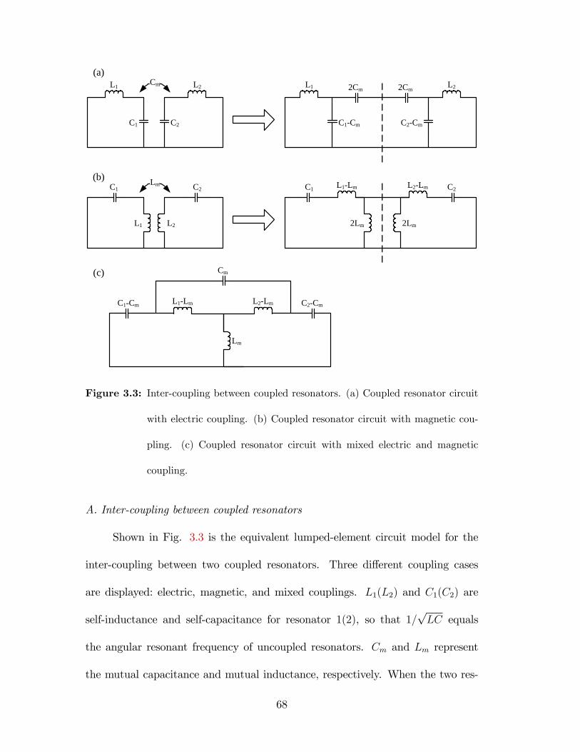
L1
C1Cm C2Cm
2Cm 2CmL2L1
C1 C2
L2Cm
LmC1 C2
L1 L2
C1 C2
Cm
2Lm 2Lm
L1LmC1Cm C2CmL2Lm
Lm
(a)
(b)
(c)
L1Lm L2Lm
Figure 3.3: Inter-coupling between coupled resonators. (a) Coupled resonator circuit
with electric coupling. (b) Coupled resonator circuit with magnetic cou-
pling. (c) Coupled resonator circuit with mixed electric and magnetic
coupling.
A. Inter-coupling between coupled resonators
Shown in Fig. 3.3 is the equivalent lumped-element circuit model for the
inter-coupling between two coupled resonators. Three di¤erent coupling cases
are displayed: electric, magnetic, and mixed couplings. L1(L2) and C1(C2) are
self-inductance and self-capacitance for resonator 1(2), so that 1=pLC equals
the angular resonant frequency of uncoupled resonators. Cm and Lm represent
the mutual capacitance and mutual inductance, respectively. When the two res-
68
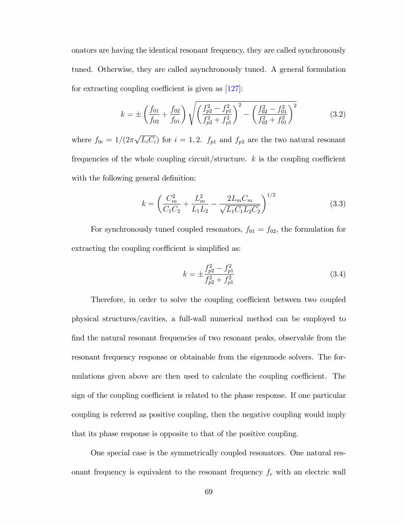
onators are having the identical resonant frequency, they are called synchronously
tuned. Otherwise, they are called asynchronously tuned. A general formulation
for extracting coupling coe¢ cient is given as [127]:
k = ��f01f02
+f02f01
�s�f 2p2 � f 2p1f 2p2 + f 2p1
�2��f 202 � f 201f 202 + f 201
�2(3.2)
where f0i = 1=(2�pLiCi) for i = 1; 2. fp1 and fp2 are the two natural resonant
frequencies of the whole coupling circuit/structure. k is the coupling coe¢ cient
with the following general de�nition:
k =
�C2mC1C2
+L2mL1L2
� 2LmCmpL1C1L2C2
�1=2(3.3)
For synchronously tuned coupled resonators, f01 = f02, the formulation for
extracting the coupling coe¢ cient is simpli�ed as:
k = �f 2p2 � f 2p1f 2p2 + f 2p1
(3.4)
Therefore, in order to solve the coupling coe¢ cient between two coupled
physical structures/cavities, a full-wall numerical method can be employed to
�nd the natural resonant frequencies of two resonant peaks, observable from the
resonant frequency response or obtainable from the eigenmode solvers. The for-
mulations given above are then used to calculate the coupling coe¢ cient. The
sign of the coupling coe¢ cient is related to the phase response. If one particular
coupling is referred as positive coupling, then the negative coupling would imply
that its phase response is opposite to that of the positive coupling.
One special case is the symmetrically coupled resonators. One natural res-
onant frequency is equivalent to the resonant frequency fe with an electric wall
69
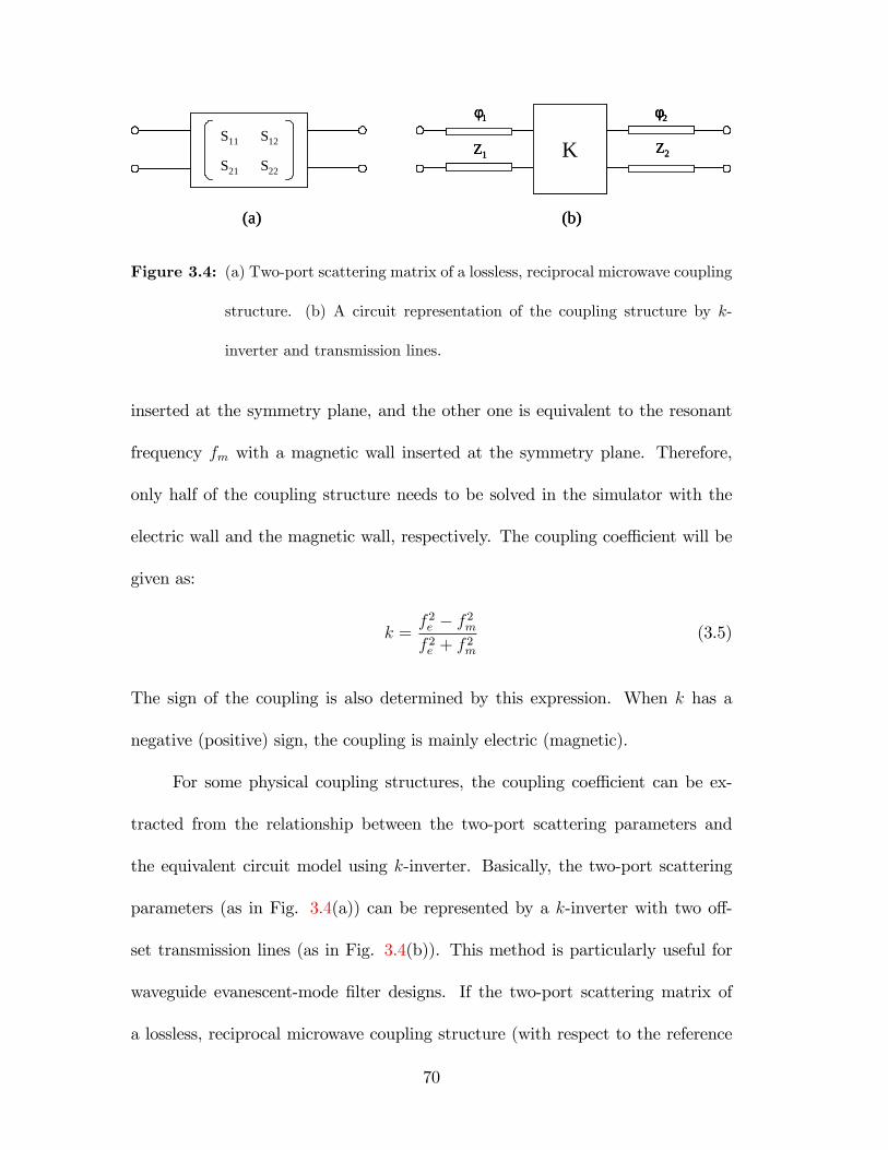
S11 S12
S21 S22
KZ1
φ2φ1
Z2
(a) (b)
S11 S12
S21 S22
S11 S12
S21 S22
KZ1
φ2φ1
Z2KZ1
φ2φ1
Z2
(a) (b)
Figure 3.4: (a) Two-port scattering matrix of a lossless, reciprocal microwave coupling
structure. (b) A circuit representation of the coupling structure by k-
inverter and transmission lines.
inserted at the symmetry plane, and the other one is equivalent to the resonant
frequency fm with a magnetic wall inserted at the symmetry plane. Therefore,
only half of the coupling structure needs to be solved in the simulator with the
electric wall and the magnetic wall, respectively. The coupling coe¢ cient will be
given as:
k =f 2e � f 2mf 2e + f 2m
(3.5)
The sign of the coupling is also determined by this expression. When k has a
negative (positive) sign, the coupling is mainly electric (magnetic).
For some physical coupling structures, the coupling coe¢ cient can be ex-
tracted from the relationship between the two-port scattering parameters and
the equivalent circuit model using k-inverter. Basically, the two-port scattering
parameters (as in Fig. 3.4(a)) can be represented by a k-inverter with two o¤-
set transmission lines (as in Fig. 3.4(b)). This method is particularly useful for
waveguide evanescent-mode �lter designs. If the two-port scattering matrix of
a lossless, reciprocal microwave coupling structure (with respect to the reference
70
planes of the discontinuities) can be solved by full-wave numerical methods, the
k value and phase o¤sets of the transmission lines can be solved as [45, 133]:
For k < 1: k =
s1� jS11j1 + jS11j
; �i = �1
2�i +
1
2�
For k > 1: k =
s1 + jS11j1� jS11j
; �i = �1
2�i; i = 1; 2 (3.6)
where S11 = jS11j ej�1, and S22 = jS22j ej�2. In practical designs, the phase o¤sets
�1 and �2 of the two transmission lines should be used to adjust the lengths of
the two coupled resonators to compensate the loading e¤ect.
B. External input and output couplings
Shown in Fig. 3.5(a) is an equivalent circuit of the external coupled resonator
structure, where R is the external coupling resistance connected to the lossless
LC resonator. In order to extract the coupling resistance R, the phase and phase
variation responses of S11 are �rstly solved. The coupling resistance R is then
calculated as [134, 135]:
R = � 4
fld�df
���min
(3.7)
where � is the phase angle of the input re�ection coe¢ cient. fl is the loaded
frequency of the resonator corresponding to the frequency point of the minimum
phase variation. Typical phase and phase variation responses are shown in Fig.
3.5(b). The external Q can be obtained as
Qe =flR
(3.8)
In practice, the phase and phase variation response of S11 of a physical
input/output coupling structure can be solved by full-wave numerical methods.
71
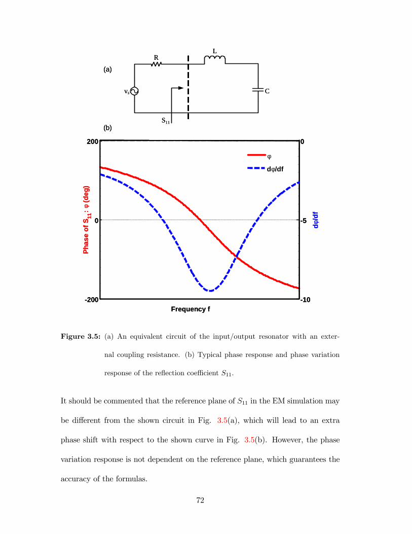
R
C
L
vs
S11
200
0
200
Phas
e of
S11
:φ(d
eg)
Frequency f10
5
0
dφ/d
f
φ
dφ/df
(a)
(b)
R
C
L
vs
S11
200
0
200
Phas
e of
S11
:φ(d
eg)
Frequency f10
5
0
dφ/d
f
φ
dφ/df
200
0
200
Phas
e of
S11
:φ(d
eg)
Frequency f10
5
0
dφ/d
f
φ
dφ/df
(a)
(b)
Figure 3.5: (a) An equivalent circuit of the input/output resonator with an exter-
nal coupling resistance. (b) Typical phase response and phase variation
response of the re�ection coe¢ cient S11.
It should be commented that the reference plane of S11 in the EM simulation may
be di¤erent from the shown circuit in Fig. 3.5(a), which will lead to an extra
phase shift with respect to the shown curve in Fig. 3.5(b). However, the phase
variation response is not dependent on the reference plane, which guarantees the
accuracy of the formulas.
72
3.2 Miniature Double-layer Coupled Stripline Res-
onator Filters in LTCC Technology
3.2.1 Introduction
Miniature broadband �lters compatible with printed circuit board (PCB) and
monolithic microwave integrated circuit (MMIC) fabrication technologies are re-
quired in many communication systems. The �lter size is usually constrained by
the size of the employed resonator structures, and the �lter bandwidth is limited
by the achievable maximum couplings between these resonators. Many available
compact resonator structures can be found in literatures. Some of them, such
as stripline resonator with one grounded end [1], hairpin resonator [136], etc.,
have the size constraint of quarter wavelength. Others, such as folded quarter-
wavelength resonator [137], ring resonator [138], spiral resonator [139], etc., have
smaller size than quarter wavelength, but are usually not applicable for broadband
�lter designs due to the di¢ culty in realizing the strong couplings.
In this section a novel double-layer coupled stripline resonator structure is
proposed to design broadband �lters with compact size less than �=8 � �=8 � h
(�lter height h is usually very small and approximately equal to the substrate
height of the stripline). The size of the proposed resonator structure can be
less than �=12, and the coupling between two resonators can be realized strong
enough for �lter designs up to 60% bandwidth by proper mechanisms. Physical
realization of the resonator structure can be easily performed in LTCC technology
73

that is a suitable manufacturing choice for high-integration level of multiple-layer
structures.
Two types of �lter con�gurations can be implemented using the proposed
resonator structures: combline and interdigital. In this section, two examples of
interdigital �lters and one example of combline �lter are designed to validate the
concept. Experimental results of the two interdigital �lters are also presented.
The two interdigital �lters have the identical speci�cations, but use di¤erent res-
onator dimensions to investigate the LTCC manufacturing e¤ects on the �lter
performance.
3.2.2 Filter Con�guration
A. Proposed Resonator Structure
The proposed double-layer coupled stripline resonator structure is shown in
Fig. 3.6. The idea is to introduce a strong capacitive loading e¤ect inside the
resonator to reduce its physical length [140]. The resonator structure consists of
two strongly coupled strips as shown in Fig. 3.6(b). The opposite ends of these
two strips are shorted to ground as in Fig. 3.6(c), so the coupling between these
two strips will behave like a capacitance that will lower the resonant frequency.
Due to this capacitive coupling e¤ect, the total physical length lr of the resonator
will be much shorter than quarter wavelength at the desired resonant frequency.
The physical length lr of the resonator is determined by three factors: the width
ws of the two strips, the coupled (overlapped) length lc, and the vertical distance
74
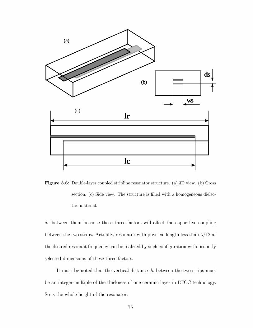
lr
lc
(a)
(b)
(c)
ws
ds
lr
lc
(a)
(b)
(c)
ws
ds
Figure 3.6: Double-layer coupled stripline resonator structure. (a) 3D view. (b) Cross
section. (c) Side view. The structure is �lled with a homogeneous dielec-
tric material.
ds between them because these three factors will a¤ect the capacitive coupling
between the two strips. Actually, resonator with physical length less than �=12 at
the desired resonant frequency can be realized by such con�guration with properly
selected dimensions of these three factors.
It must be noted that the vertical distance ds between the two strips must
be an integer-multiple of the thickness of one ceramic layer in LTCC technology.
So is the whole height of the resonator.
75
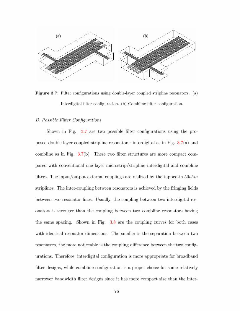
(a) (b)(a) (b)
Figure 3.7: Filter con�gurations using double-layer coupled stripline resonators. (a)
Interdigital �lter con�guration. (b) Combline �lter con�guration.
B. Possible Filter Con�gurations
Shown in Fig. 3.7 are two possible �lter con�gurations using the pro-
posed double-layer coupled stripline resonators: interdigital as in Fig. 3.7(a) and
combline as in Fig. 3.7(b). These two �lter structures are more compact com-
pared with conventional one layer microstrip/stripline interdigital and combline
�lters. The input/output external couplings are realized by the tapped-in 50ohm
striplines. The inter-coupling between resonators is achieved by the fringing �elds
between two resonator lines. Usually, the coupling between two interdigital res-
onators is stronger than the coupling between two combline resonators having
the same spacing. Shown in Fig. 3.8 are the coupling curves for both cases
with identical resonator dimensions. The smaller is the separation between two
resonators, the more noticeable is the coupling di¤erence between the two con�g-
urations. Therefore, interdigital con�guration is more appropriate for broadband
�lter designs, while combline con�guration is a proper choice for some relatively
narrower bandwidth �lter designs since it has more compact size than the inter-
76
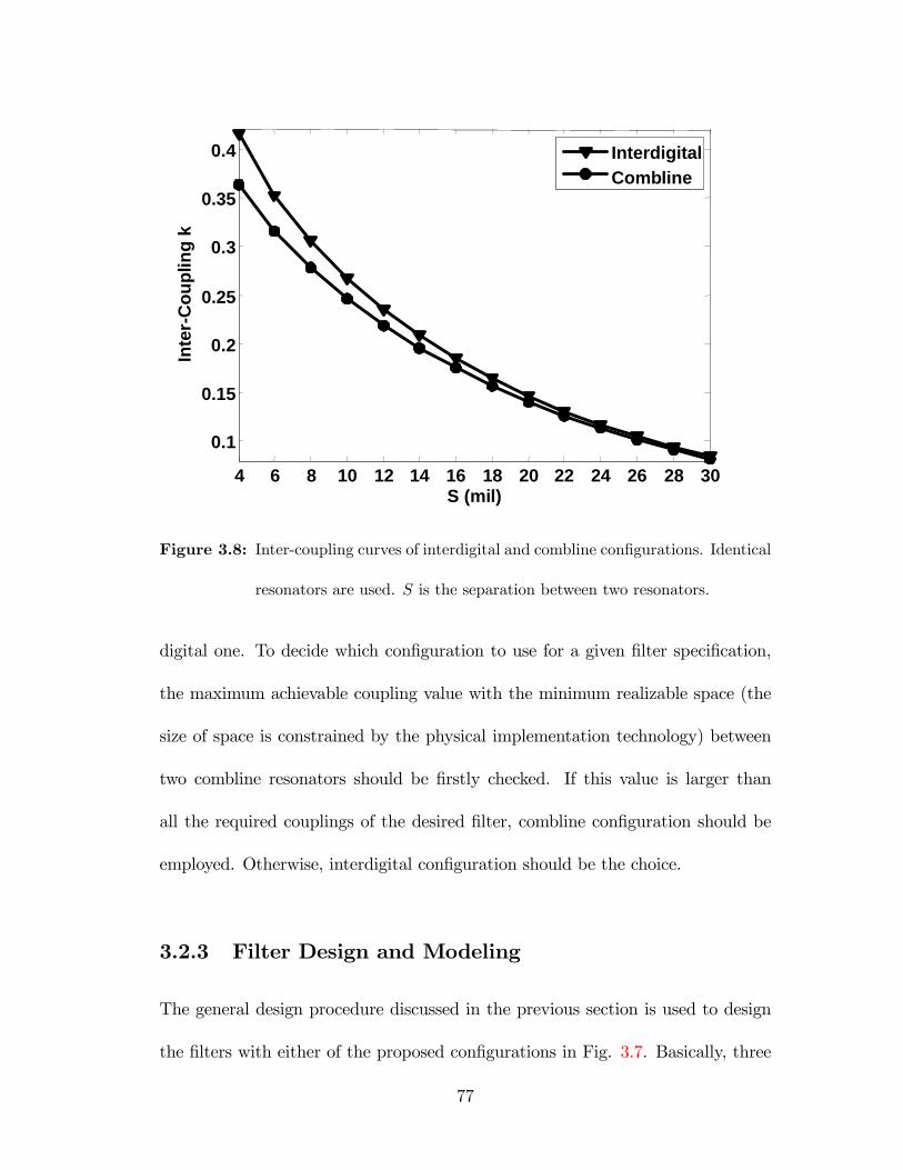
4 6 8 10 12 14 16 18 20 22 24 26 28 30
0.1
0.15
0.2
0.25
0.3
0.35
0.4
S (mil)
Inte
rC
oupl
ing
k
InterdigitalCombline
4 6 8 10 12 14 16 18 20 22 24 26 28 30
0.1
0.15
0.2
0.25
0.3
0.35
0.4
S (mil)
Inte
rC
oupl
ing
k
InterdigitalCombline
Figure 3.8: Inter-coupling curves of interdigital and combline con�gurations. Identical
resonators are used. S is the separation between two resonators.
digital one. To decide which con�guration to use for a given �lter speci�cation,
the maximum achievable coupling value with the minimum realizable space (the
size of space is constrained by the physical implementation technology) between
two combline resonators should be �rstly checked. If this value is larger than
all the required couplings of the desired �lter, combline con�guration should be
employed. Otherwise, interdigital con�guration should be the choice.
3.2.3 Filter Design and Modeling
The general design procedure discussed in the previous section is used to design
the �lters with either of the proposed con�gurations in Fig. 3.7. Basically, three
77

main steps are implemented: i) Initial �lter dimensions are determined according
to the given �lter speci�cations. ii) Optimization using MMM is performed to
�nd the optimum �lter dimensions. iii) Ansoft HFSS is employed to check the
optimum design from the second step and �ne-tune the �lter dimensions if needed.
The detailed information of each step is illustrated below.
A. Initial Design
Given the speci�cations of a desired �lter, the �lter design starts with synthe-
sizing a circuit model prototype. Physical realization is then performed according
to such ideal model. The initial design procedure for the presented �lters is given
as follows.
1. An ideal circuit model is generated according to the �lter requirements [1].
2. The dimensions of the double-layer coupled stripline resonator are deter-
mined in terms of the center frequency of the �lter.
3. Determine the tapped-in stripline position to achieve the external coupling
R [111].
4. Determine the separations between resonators to provide the required inter-
couplings [127].
5. Assemble the tapped-lines and resonators together according to the cal-
culated dimensions. Initial �lter responses can be obtained by full-wave
electromagnetic simulation in MMM or HFSS.
One of the advantages of combline and interdigital �lters is that the resonant
78

frequency of the resonators will not be changed much by the loading e¤ects of the
couplings. Therefore, the initial �lter response is usually a good starting point
(typically return loss is below 10 dB) for further optimization.
B. Optimization by MMM
The initial design procedure given above does not take into account the
higher order modes and the non-adjacent couplings between resonators, which
have more e¤ects on broadband �lter designs than narrow-band ones. To achieve
the desired �lter performance, optimization by MMM can be employed. To
demonstrate the optimization procedure by MMM, an interdigital �lter con�g-
uration is used (Combline case is similar).
Shown in Fig. 3.9(a) is an interdigital �lter with two stripline ports along
z-axis. To model this �lter con�guration, the MMM should be applied along
the z-direction. The cross sections involved are a stripline (I), an asymmetric
stripline (II), side view of double-layer coupled stripline resonator (III), a rectan-
gular waveguide (IV), and so on (as in Fig. 3.9(b)). Eigenmodes and eigen�elds
of these cross sections can be solved by the GTR technique (see Appendix A, p.
255). The typical electric �eld distributions of the fundamental mode of section
(I) and (III) are shown in Appendix B (Fig. B.1(a) and (b), p. 269). The discon-
tinuities between the cross sections are modeled by GSMs that can be obtained by
MMM program based on the formulations in Appendix C (p. 271). Finally, the
overall response can be computed by cascading all the GSMs together using (1.2).
In principle this MMM approach is rigorous, but the convergence and simulation
speed must be considered. The rectangular waveguides separating the discontinu-
79
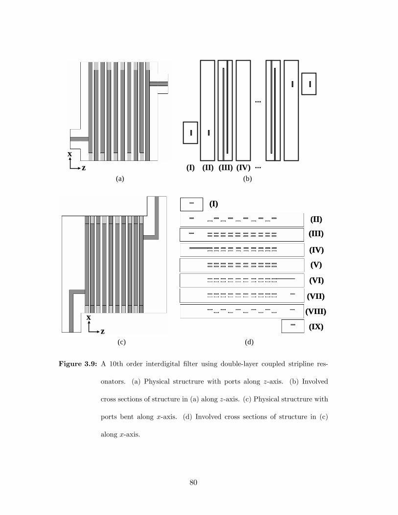
(a) (b)
...
(I) (II) (III) (IV) ...x
z
xz
(I)
(II)
(III)
(IV)
(V)
(VI)
(VII)
(VIII)
(IX)
(I)
(II)
(III)
(IV)
(V)
(VI)
(VII)
(VIII)
(IX)
(c) (d)
Figure 3.9: A 10th order interdigital �lter using double-layer coupled stripline res-
onators. (a) Physical structrure with ports along z-axis. (b) Involved
cross sections of structure in (a) along z-axis. (c) Physical structrure with
ports bent along x-axis. (d) Involved cross sections of structure in (c)
along x-axis.
80
ities are very short, and the fundamental resonating modes of the interdigital �lter
are mainly operating with TEMx �elds, while the �elds in cross sections of III, IV,
etc. are presented as a summation of TEz and TMz modes in the MMM analy-
sis. As a consequence, a very large number of modes are needed for convergence,
which would result in large computation time and numerical errors. Therefore,
this approach is not appropriate for optimization.
Shown in Fig. 3.9(c) is the same �lter as in Fig. 3.9(a) with 90� bends
added at the input and output ports along x-direction. MMM simulation can,
therefore, be applied along x-direction for this transformed topology. The bene�t
of doing MMM simulation along x-direction is that the fundamental modes of
the cross-sections along x-axis will be TEMx modes, which correspond to the
main operating resonant modes of the �lter. This means that MMM simulation
with only TEMx modes can generate acceptable results close to the converged
ones (actually, the e¤ects of non-adjacent couplings are included in these TEMx
modes). MMM simulation with only TEMx modes is also fast and appropriate
for optimization. The same situation can also be found in [35] for conventional
interdigital �lters.
For the �lter structure In Fig. 3.9(c), there are several cross sections involved
along x-direction, and some of them have N � 1 internal conductors. For these
cross sections, N orthogonal TEMx modes exist and must be included in the
MMM simulation. Shown in Fig. 3.9(d) are the nine cross sections of the �lter
topology in Fig. 3.9(c) along positive x-direction in sequence. The number of
TEMx modes for each section is: one TEMx mode in section (I) and (IX), eleven
81
TEMx modes in section (II) and (VIII), twenty TEMx modes in section (IV),
(V) and (VI), and twenty-one TEMx modes in section (III) and (VII). The GTR
technique is well suited to calculate the eigenmodes and eigen�elds of these cross
sections (A computer program has been created for generalized waveguide cross-
sections based on the GTR formulations in Appendix A, p. 255). Shown in Fig.
B.1(e) (p. 269) are the typical electric �eld distribution of two TEMx modes of
cross-section (V) (Totally 20 orthogonal TEMx modes exist inside section (V).),
from which the interactions between non-adjacent strips can be noticed. Actually,
these interactions are corresponding to the non-adjacent couplings between the
resonators.
After the eigen�elds of all the TEMx modes have been solved for each cross
section, the discontinuities between these cross sections can be characterized by
GSMs (Computer program can be created based on the formulations in Appendix
C, p. 271) and the overall response can be obtained by means of GSM cascading
using (1.2). In order to have more accurate response, higher order TE and TM
modes should be included for the simulation.
For the odd-order �lter as shown in Fig. 3.10, the structure is symmetric
about the middle plane. In order to analyze this structure, MMM simulation is
performed twice on the one-port half structure separated by the middle plane:
once is placing a perfect electric wall (PEW, corresponding to short circuit) at
the symmetry plane, and the other once is placing a perfect magnetic wall (PMW,
corresponding to open circuit) at the symmetry plane. Two results of re�ection
coe¢ cients S11e and S11m are obtained from the MMM simulation corresponding
82
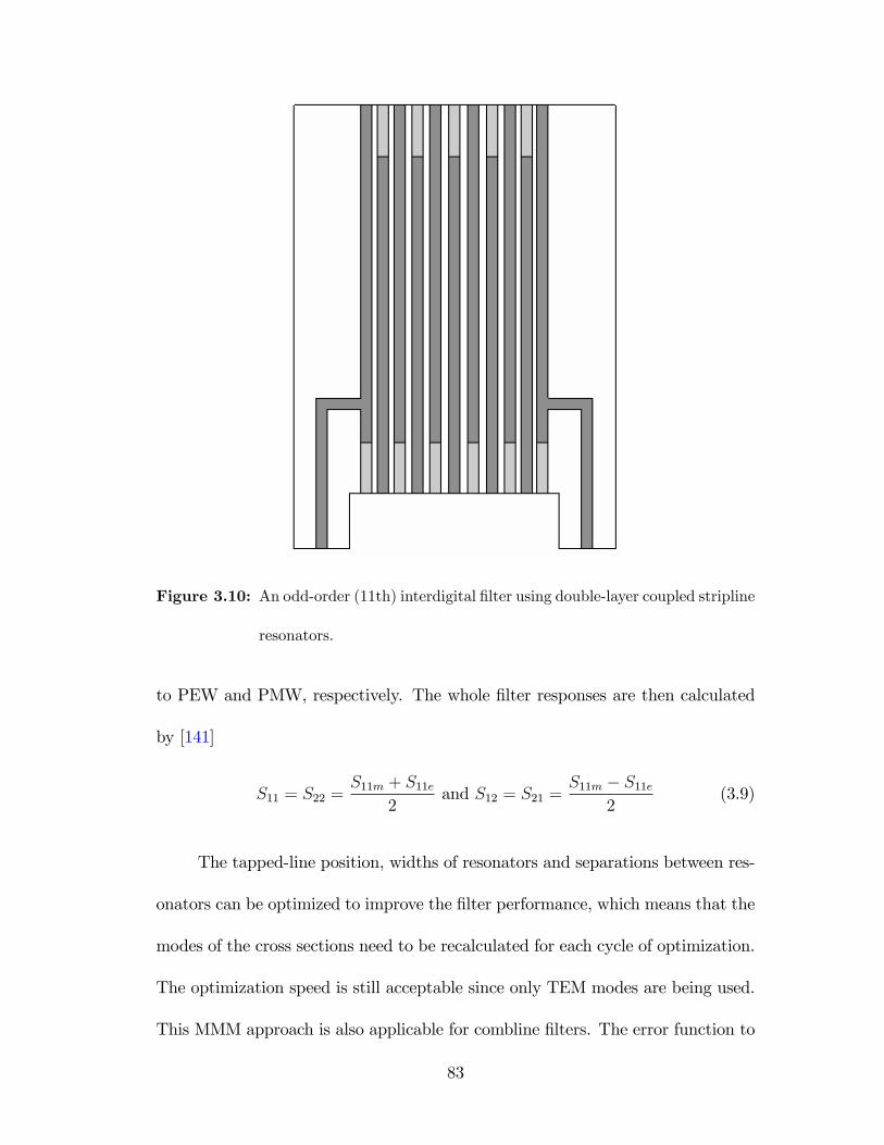
Figure 3.10: An odd-order (11th) interdigital �lter using double-layer coupled stripline
resonators.
to PEW and PMW, respectively. The whole �lter responses are then calculated
by [141]
S11 = S22 =S11m + S11e
2and S12 = S21 =
S11m � S11e2
(3.9)
The tapped-line position, widths of resonators and separations between res-
onators can be optimized to improve the �lter performance, which means that the
modes of the cross sections need to be recalculated for each cycle of optimization.
The optimization speed is still acceptable since only TEM modes are being used.
This MMM approach is also applicable for combline �lters. The error function to
83
be minimized for the optimization is constructed depending on the locations of
the poles (fpi) and equiripple points (fei).
err =
NpXi=1
wpi jS11(fpi)j2 +NeXi=1
wei (jS11(fei)j � ")2 (3.10)
where Np and Ne are the number of poles and equiripple points, respectively. wp
and we are the optimization weights. " represents the equiripple return loss.
C. Fine-Tuning in HFSS (if needed)
The simulated �lter response by MMM with only TEM modes might be
di¤erent from the converged one. Many higher order TE and TM modes must be
included in MMM simulation to obtain the converged response, which makes the
�nal tuning too di¢ cult since the modes of cross sections have to be recalculated
each time. Hence, Ansoft HFSS is then applied to verify the design and �ne-tune
the �lter if needed. The parameter extraction method [119] can be employed to
guide the �ne-tuning in HFSS to speed up the procedure. Basically, only the
tapped-line position and the width of the �rst resonator are needed to be tuned
in this step.
HFSS is not used in the previous optimization step because of the slow
simulation speed. For the design examples given next, it takes MMM about �ve
hours and 1000 iterations to generate the desired performance after the eigenmodes
and eigen�elds have been calculated (150 modes are used). While it takes HFSS
more than six hours to obtain the converged response for one single �lter structure.
For an optimization procedure of 1000 iterations, it will take HFSS about 6000
hours to acquire the optimum performance, which is not acceptable in practice.
84
A desktop PC using 3.0-GHz Pentium 4 processor and 4-GB memory is employed
to perform the simulations.
3.2.4 Design Examples
Three design examples are performed to show the feasibility. Two interdigital
�lters with the same speci�cations but di¤erent resonator dimensions are man-
ufactured to investigate the e¤ects of the LTCC manufacturing procedure. One
combline �lter is designed only for demonstration.
A. Design Example I
A design of a ten-pole Chebyshev �lter with a center frequency of 1.125 GHz
and 500-MHz bandwidth is performed. The relative bandwidth is about 45%. The
desired stopband rejection level below 0.75 GHz and above 1.5 GHz must be larger
than 50 dB. The external couplings and the normalized inter-couplings are
Rin = Rout = 0:98562 m1;2 = m9;10 = 0:81907
m2;3 = m8;9 = 0:58576 m3;4 = m7;8 = 0:54538
m4;5 = m6;7 = 0:53288 m5;6 = 0:52976
(3.11)
The interdigital �lter con�guration to be employed is shown in Fig. 3.9(c).
This �lter will be embedded inside a PCB system using LTCC technology, and
the stack-up options with other components set many constraints on the vertical
dimensions. Shown in Fig. 3.11 is the end view of the �lter along x-direction.
The height of the whole �lter box is h = 59:28mil, the vertical position of the
lower strip is h1 = 25:94mil, and the vertical position of the upper strip is h2 =
29:69mil. Only one ceramic layer (thickness is about 3:74mil) exists between the
85
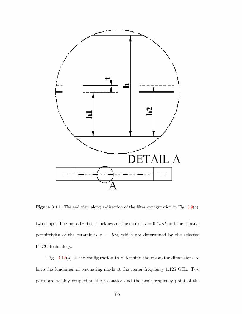
Figure 3.11: The end view along x-direction of the �lter con�guration in Fig. 3.9(c).
two strips. The metallization thickness of the strip is t = 0:4mil and the relative
permittivity of the ceramic is "r = 5:9, which are determined by the selected
LTCC technology.
Fig. 3.12(a) is the con�guration to determine the resonator dimensions to
have the fundamental resonating mode at the center frequency 1.125 GHz. Two
ports are weakly coupled to the resonator and the peak frequency point of the
86
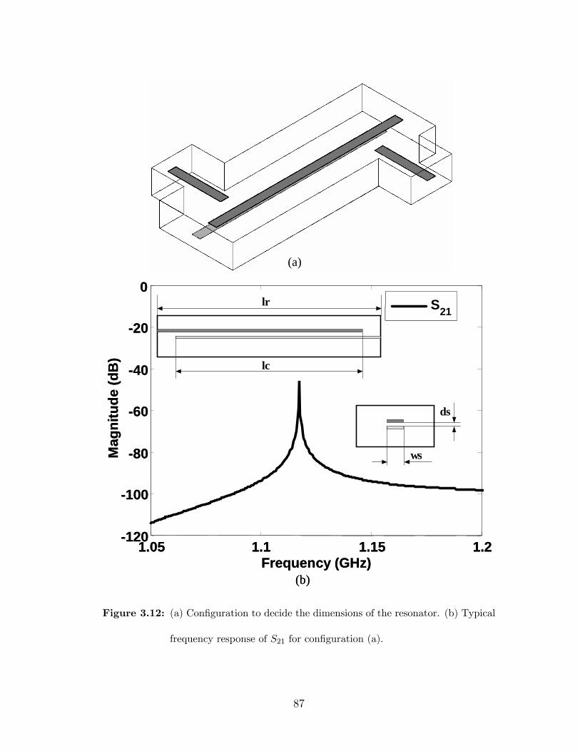
1.05 1.1 1.15 1.2120
100
80
60
40
20
0
Mag
nitu
de (d
B)
Frequency (GHz)
S21
(b)
lr
lc
ws
ds
(a)
1.05 1.1 1.15 1.2120
100
80
60
40
20
0
Mag
nitu
de (d
B)
Frequency (GHz)
S21
(b)
lr
lc
ws
ds
(a)
Figure 3.12: (a) Con�guration to decide the dimensions of the resonator. (b) Typical
frequency response of S21 for con�guration (a).
87

simulated S21 response as in Fig. 3.12(b) is the resonant frequency. The length lr
of the resonator is selected as lr = 500mil. The coupled length lc and width ws
of the two strips (two strips in one resonator have the same dimensions) are being
swept until the required resonant frequency 1.125 GHz is achieved. The found
values are lc = 420mil and ws = 20mil.
The con�guration for computing the external coupling is shown in Fig.
3.13(a). The coupling extraction method is discussed in the previous section.
Basically, the re�ection coe¢ cient S11 is obtained by MMM with respect to the
di¤erent tapped-in positions (htapin in Fig. 3.13(b)), and equation (3.7) is used
to calculate the coupling values. The external coupling curve is presented in Fig.
3.13(b), which shows the external coupling is linearly proportional to the tapped-
in position. The value of htapin to have R = 0:98562 is about 432mil.
Fig. 3.14(a) shows the con�guration to calculate the inter-coupling value,
in which the two ports are very weakly coupled to the coupled resonator struc-
ture. The typical simulated magnitude and phase responses of such con�guration
are displayed in Fig. 3.14(b), where two peak frequency points correspond to
the natural frequencies. The inter-coupling value k can be calculated by (3.4)
with respect to the di¤erent separations between the resonators. The computed
inter-coupling curve is shown in Fig. 3.15 and the separations are calculated by
interpolation to have the desired inter-coupling values. The found separations for
the �ve desired adjacent couplings in (3.11) are: S1 = 7:1mil, S2 = 11:9mil,
S3 = 13:0mil, S4 = 13:4mil, and S5 = 13:5mil, respectively (variable de�ni-
tions are given in Fig. 3.17). The relationship between k and the normalized
88
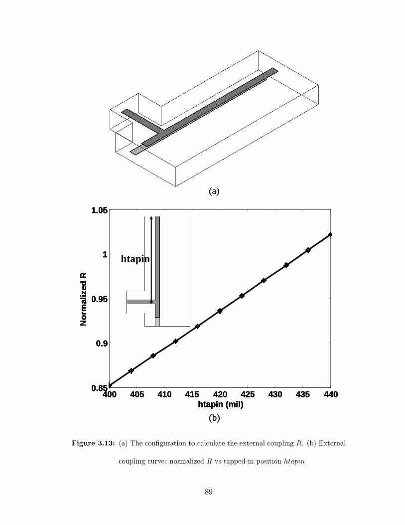
400 405 410 415 420 425 430 435 4400.85
0.9
0.95
1
1.05
htapin (mil)
Nor
mal
ized
R
htapin
(a)
(b)
400 405 410 415 420 425 430 435 4400.85
0.9
0.95
1
1.05
htapin (mil)
Nor
mal
ized
R
htapin
400 405 410 415 420 425 430 435 4400.85
0.9
0.95
1
1.05
htapin (mil)
Nor
mal
ized
R
htapin
(a)
(b)
Figure 3.13: (a) The con�guration to calculate the external coupling R. (b) External
coupling curve: normalized R vs tapped-in position htapin
89
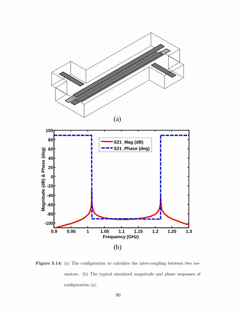
0.9 0.95 1 1.05 1.1 1.15 1.2 1.25 1.3
100
80
60
40
20
0
20
40
60
80
100
Mag
nitu
de (d
B) &
Pha
se (d
eg)
Frequency (GHz)
S21_Mag (dB)S21_Phase (deg)
0.9 0.95 1 1.05 1.1 1.15 1.2 1.25 1.3
100
80
60
40
20
0
20
40
60
80
100
Mag
nitu
de (d
B) &
Pha
se (d
eg)
Frequency (GHz)
S21_Mag (dB)S21_Phase (deg)
(a)
(b)
Figure 3.14: (a) The con�guration to calculate the inter-coupling between two res-
onators. (b) The typical simulated magnitude and phase responses of
con�guration (a).
90
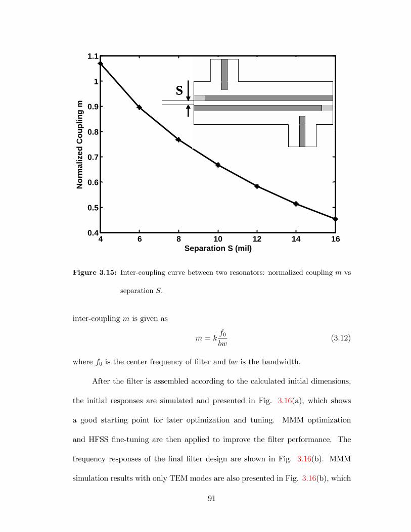
4 6 8 10 12 14 160.4
0.5
0.6
0.7
0.8
0.9
1
1.1
Separation S (mil)
Nor
mal
ized
Cou
plin
g m
S
4 6 8 10 12 14 160.4
0.5
0.6
0.7
0.8
0.9
1
1.1
Separation S (mil)
Nor
mal
ized
Cou
plin
g m
4 6 8 10 12 14 160.4
0.5
0.6
0.7
0.8
0.9
1
1.1
Separation S (mil)
Nor
mal
ized
Cou
plin
g m
SS
Figure 3.15: Inter-coupling curve between two resonators: normalized coupling m vs
separation S.
inter-coupling m is given as
m = kf0bw
(3.12)
where f0 is the center frequency of �lter and bw is the bandwidth.
After the �lter is assembled according to the calculated initial dimensions,
the initial responses are simulated and presented in Fig. 3.16(a), which shows
a good starting point for later optimization and tuning. MMM optimization
and HFSS �ne-tuning are then applied to improve the �lter performance. The
frequency responses of the �nal �lter design are shown in Fig. 3.16(b). MMM
simulation results with only TEM modes are also presented in Fig. 3.16(b), which
91
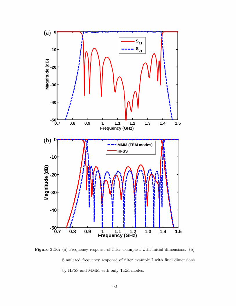
0.7 0.8 0.9 1 1.1 1.2 1.3 1.4 1.550
40
30
20
10
0
Mag
nitu
de (d
B)
Frequency (GHz)
S11
S21
0.7 0.8 0.9 1 1.1 1.2 1.3 1.4 1.550
40
30
20
10
0
Mag
nitu
de (d
B)
Frequency (GHz)
MMM (TEM modes)HFSS
(a)
(b)
0.7 0.8 0.9 1 1.1 1.2 1.3 1.4 1.550
40
30
20
10
0
Mag
nitu
de (d
B)
Frequency (GHz)
S11
S21
0.7 0.8 0.9 1 1.1 1.2 1.3 1.4 1.550
40
30
20
10
0
Mag
nitu
de (d
B)
Frequency (GHz)
S11
S21
0.7 0.8 0.9 1 1.1 1.2 1.3 1.4 1.550
40
30
20
10
0
Mag
nitu
de (d
B)
Frequency (GHz)
MMM (TEM modes)HFSS
0.7 0.8 0.9 1 1.1 1.2 1.3 1.4 1.550
40
30
20
10
0
Mag
nitu
de (d
B)
Frequency (GHz)
MMM (TEM modes)HFSS
(a)
(b)
Figure 3.16: (a) Frequency response of �lter example I with initial dimensions. (b)
Simulated frequency response of �lter example I with �nal dimensions
by HFSS and MMM with only TEM modes.
92
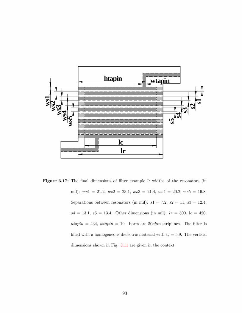
lr
htapin wtapin
ws1
ws2
ws3
ws4
ws5
s1s2s3
s4s5
lc
Figure 3.17: The �nal dimensions of �lter example I: widths of the resonators (in
mil): ws1 = 21:2, ws2 = 23:1, ws3 = 21:4, ws4 = 20:2, ws5 = 19:8.
Separations between resonators (in mil): s1 = 7:2, s2 = 11, s3 = 12:4,
s4 = 13:1, s5 = 13:4. Other dimensions (in mil): lr = 500, lc = 420,
htapin = 434, wtapin = 19. Ports are 50ohm striplines. The �lter is
�lled with a homogeneous dielectric material with "r = 5:9. The vertical
dimensions shown in Fig. 3.11 are given in the context.
93

shows the feasibility of optimization by MMM (The frequency shift can be taken
into account during the optimization). The �nal dimensions of the �lter structure
are given in the caption of Fig. 3.17.
The minimum return loss over the passband is about 15 dB because the non-
adjacent couplings for such broadband �lter are not avoidable and make it very
di¢ cult to achieve a return loss better than 15 dB. The upper stopband of this
�lter has clean spurious response up to the third harmonic. The �nal dimension
of the whole �lter box is about 500mil � 515mils � 59:28mil, which is less than
�=8� �=8� h = 540mil� 540mil� 59:28mil at the center frequency 1.125 GHz.
This �lter is manufactured in LTCC technology for testing. Fig. 3.18(a)
shows the �lter prototype and the arrangement of the measurement. Input and
output ports of the �lter are bent toward the same direction for the convenience to
connect with other components. Transitions from 50Ohm microstrip lines to the
tapped-in striplines are also added on the �lter. J-probe launches and a Cascade
Microwave Probe Station are used in the measurement. The measured response
is shown in Fig. 3.19(a). The insertion loss at the center frequency is about 3
dB and at the higher band edge is about 6 dB. The wideband response shows
that the spurious response starts around 3.6 GHz that is about three harmonics.
A simulation by HFSS with lossy materials is also performed to investigate the
response di¤erence between the designed and manufactured �lters. The employed
parameters for loss are: �nite conductivity � = 13100000 S=m for conductor and
loss tangent of 0.001 for ceramics. Both the simulated and measured responses
are shown in Fig. 3.19(b). A good agreement is noticed except a frequency
94
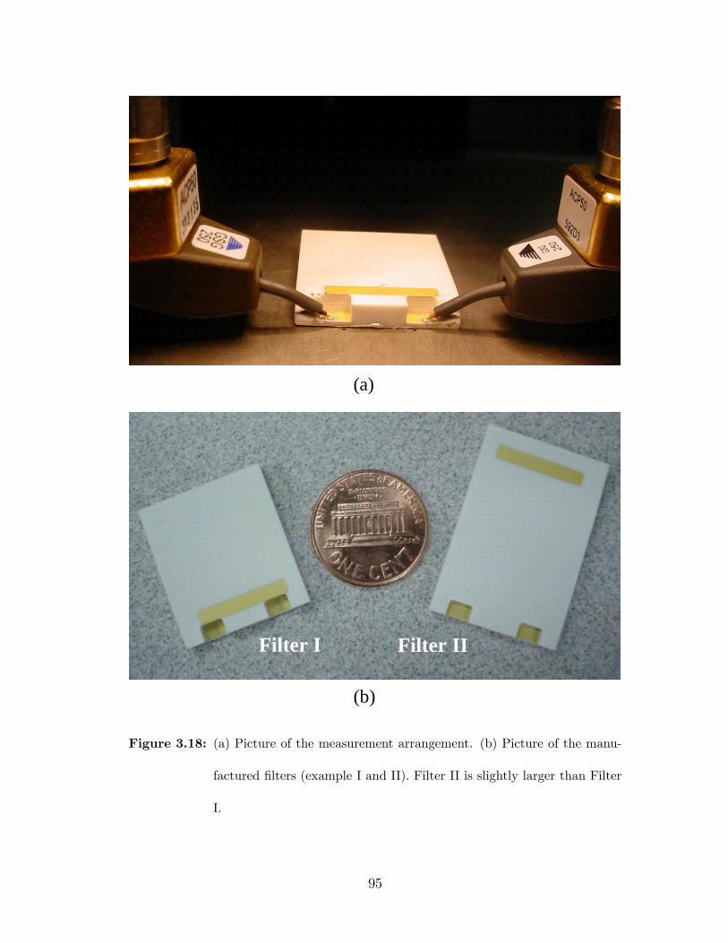
Filter I Filter IIFilter I Filter II
(a)
(b)
Figure 3.18: (a) Picture of the measurement arrangement. (b) Picture of the manu-
factured �lters (example I and II). Filter II is slightly larger than Filter
I.
95
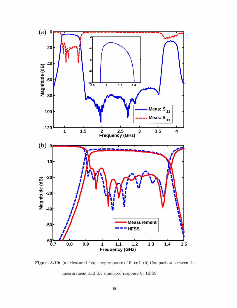
1 1.5 2 2.5 3 3.5 4120
100
80
60
40
20
0
Frequency (GHz)
Mag
nitu
de (d
B)
Meas: S 21
Meas: S 11
1 1.5 2 2.5 3 3.5 4120
100
80
60
40
20
0
Frequency (GHz)
Mag
nitu
de (d
B)
Meas: S 21
Meas: S 11
0.7 0.8 0.9 1 1.1 1.2 1.3 1.4 1.560
50
40
30
20
10
0
Frequency (GHz)
Mag
nitu
de (d
B)
MeasurementHFSS
0.7 0.8 0.9 1 1.1 1.2 1.3 1.4 1.560
50
40
30
20
10
0
Frequency (GHz)
Mag
nitu
de (d
B)
MeasurementHFSS
(a)
(b)
0.8 1 1.2 1.410
8
6
4
2
0.8 1 1.2 1.410
8
6
4
2
Figure 3.19: (a) Measured frequency response of �lter I. (b) Comparison between the
measurement and the simulated response by HFSS.
96

shift between them. The frequency shift is caused by the e¤ects of the LTCC
manufacturing procedure, such as vias, inhomogeneous ceramic layers, etc. (In
HFSS simulation, solid walls and homogeneous materials are assumed.), which
will be discussed later.
B. Design Example II
In design example I, one ceramic layer of thickness ds = 3:74mil exists be-
tween the two strips of a resonator. To investigate the sensitivity of the �lter
with respect to ds and the e¤ects of the LTCC manufacturing procedure on �lter
performance, a second design with larger ds is carried out for an odd-order inter-
digital �lter. The �lter requirements are identical with design example I, but a
design of an eleven-pole �lter is performed for this example. The stack-up option
is di¤erent from example I. For this example, h1 = 29:68mil, h2 = 37:08mil,
and h = 63:02mil. De�nitions of h1, h2 and h are given as in Fig. 3.11. The
separation between the two strips is ds = h2�h1 = 7:4mil, which means that the
physical length of the resonator will be longer than example I due to the relatively
weaker coupling between two strips. The selected dimensions of the resonator are:
lr = 700mil, lc = 516mil, and ws = 20mil.
The same design procedure as example I is followed for this design. The
�nal dimensions of the �lter structure are given in Table 3.2. The volume of the
whole �lter box is about 700mil � 540mils� 63:02mil that is larger than design
example I. Fig. 3.18(b) shows both manufactured �lters of example I and II. The
measured response is shown in Fig. 3.20(a). The spurious response starts around
2.5 GHz that is about two harmonics. The reason that �lter II has worse spurious
97
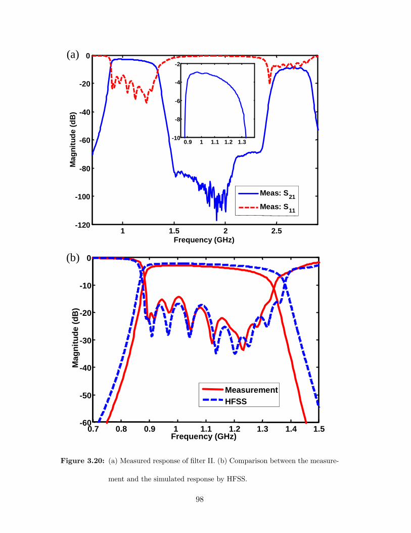
1 1.5 2 2.5120
100
80
60
40
20
0
Frequency (GHz)
Mag
nitu
de (d
B)
Meas: S21
Meas: S11
1 1.5 2 2.5120
100
80
60
40
20
0
Frequency (GHz)
Mag
nitu
de (d
B)
Meas: S21
Meas: S11
0.9 1 1.1 1.2 1.310
8
6
4
2
0.9 1 1.1 1.2 1.310
8
6
4
2
0.7 0.8 0.9 1 1.1 1.2 1.3 1.4 1.560
50
40
30
20
10
0
Frequency (GHz)
Mag
nitu
de (d
B)
MeasurementHFSS
0.7 0.8 0.9 1 1.1 1.2 1.3 1.4 1.560
50
40
30
20
10
0
Frequency (GHz)
Mag
nitu
de (d
B)
MeasurementHFSS
(a)
(b)
Figure 3.20: (a) Measured response of �lter II. (b) Comparison between the measure-
ment and the simulated response by HFSS.
98
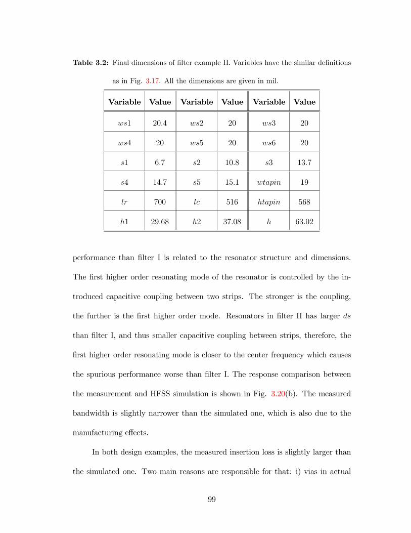
Table 3.2: Final dimensions of �lter example II. Variables have the similar de�nitions
as in Fig. 3.17. All the dimensions are given in mil.
Variable Value Variable Value Variable Value
ws1 20:4 ws2 20 ws3 20
ws4 20 ws5 20 ws6 20
s1 6:7 s2 10:8 s3 13:7
s4 14:7 s5 15:1 wtapin 19
lr 700 lc 516 htapin 568
h1 29:68 h2 37:08 h 63:02
performance than �lter I is related to the resonator structure and dimensions.
The �rst higher order resonating mode of the resonator is controlled by the in-
troduced capacitive coupling between two strips. The stronger is the coupling,
the further is the �rst higher order mode. Resonators in �lter II has larger ds
than �lter I, and thus smaller capacitive coupling between strips, therefore, the
�rst higher order resonating mode is closer to the center frequency which causes
the spurious performance worse than �lter I. The response comparison between
the measurement and HFSS simulation is shown in Fig. 3.20(b). The measured
bandwidth is slightly narrower than the simulated one, which is also due to the
manufacturing e¤ects.
In both design examples, the measured insertion loss is slightly larger than
the simulated one. Two main reasons are responsible for that: i) vias in actual
99

structures might introduce more loss than the solid wall model in HFSS and ii)
the loss tangent of the actual ceramic material is larger than 0.001.
C. Design Example III
A combline �lter is also designed to show the feasibility of applying double-
layer coupled stripline resonators for combline �lter con�guration as in Fig. 3.7(b).
A design of six-pole �lter with center frequency 1.1 GHz and 15% bandwidth is
performed. The design procedure is exactly same as the previous two examples,
except that di¤erent cross sections are used for MMM modeling. The �lter struc-
ture and simulated frequency response are shown in Fig. 3.21.
3.2.5 LTCC Manufacturing E¤ects
The measured responses of example I and II are slightly di¤erent from the simu-
lated ones, which is usually caused by the LTCC manufacturing e¤ects. Shown in
Fig. 3.22 is a draft of the physical realization of the designed �lters in LTCC tech-
nology. Basically, the �lled ceramic is placed layer by layer with �xed thickness of
each layer. The horizontal walls and the resonator striplines inside the ceramic are
implemented by metallization of gold. The vertical walls are realized by via fence
of closely-placed vias. If the signal is communicating between di¤erent layers, vias
are also applied to connect the signal lines. Such a manufacturing procedure will
a¤ect the �lter performance from several points of views.
First, the via fence to realize the vertical walls of the �lter will a¤ect the
resonator length, which can be observed from the zoom-in view in Fig. 3.22.
100
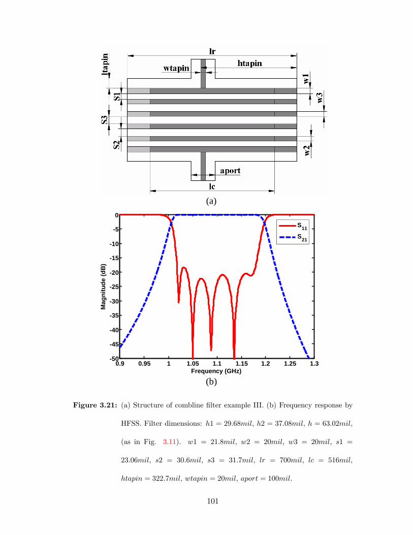
0.9 0.95 1 1.05 1.1 1.15 1.2 1.25 1.350
45
40
35
30
25
20
15
10
5
0
Mag
nitu
de (d
B)
Frequency (GHz)
S11
S21
0.9 0.95 1 1.05 1.1 1.15 1.2 1.25 1.350
45
40
35
30
25
20
15
10
5
0
Mag
nitu
de (d
B)
Frequency (GHz)
S11
S21
(a)
(b)
Figure 3.21: (a) Structure of combline �lter example III. (b) Frequency response by
HFSS. Filter dimensions: h1 = 29:68mil, h2 = 37:08mil, h = 63:02mil,
(as in Fig. 3.11). w1 = 21:8mil, w2 = 20mil, w3 = 20mil, s1 =
23:06mil, s2 = 30:6mil, s3 = 31:7mil, lr = 700mil, lc = 516mil,
htapin = 322:7mil, wtapin = 20mil, aport = 100mil.
101
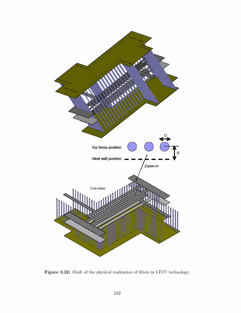
S
D
Via fence position
Ideal wall position
Cutview
Zoomin
S
D
Via fence position
Ideal wall position
Cutview
Zoomin
Figure 3.22: Draft of the physical realization of �lters in LTCC technology.
102

Diameter D of vias is about 6mil. The distance between two vias should be
selected to be as small as possible to decrease the parasitic resistance and also
create an e¤ective �pure resistance� environment (i.e. parasitic inductance and
capacitance are counteracted.), which is usually decided experimentally. The via
fence position relative to the ideal vertical wall position (S in Fig. 3.22) should be
determined to have the manufactured resonator resonating at the same frequency
as the ideal resonator, otherwise, the actual �lter response will be shifted from
the designed one. The optimum via fence position is about S = D=4.
Second, the thickness of gold metallization usually varies from 0:4mil to
0:6mil. This e¤ect will cause the variation of the vertical distance ds (as in
Fig. 3.6) between two strips in a resonator, and thus the frequency shift of the
resonators. The �lters designed with smaller ds will be in�uenced more by this
e¤ect than those with larger ds since the variation occupies more percentage in
smaller ds. This might be one of the reasons that the measured response of �lter
I is shifted from the desired center frequency.
Third, assembling the �lled ceramic layer by layer causes the variation of
the permittivity of di¤erent layers, i.e. the �lled ceramic is not perfectly homoge-
neous. The relative permittivity can be from 4.7 to 6.3. This e¤ect will cause the
frequency shift and mainly in�uence all the couplings existing in the �lters. The
�lters with larger ds will be a¤ected more since larger ds means greater variation
of the permittivity. This could be one of the reasons that �lter II has narrower
bandwidth than the designed one.
In the actual manufacture, several test pieces are usually manufactured and
103
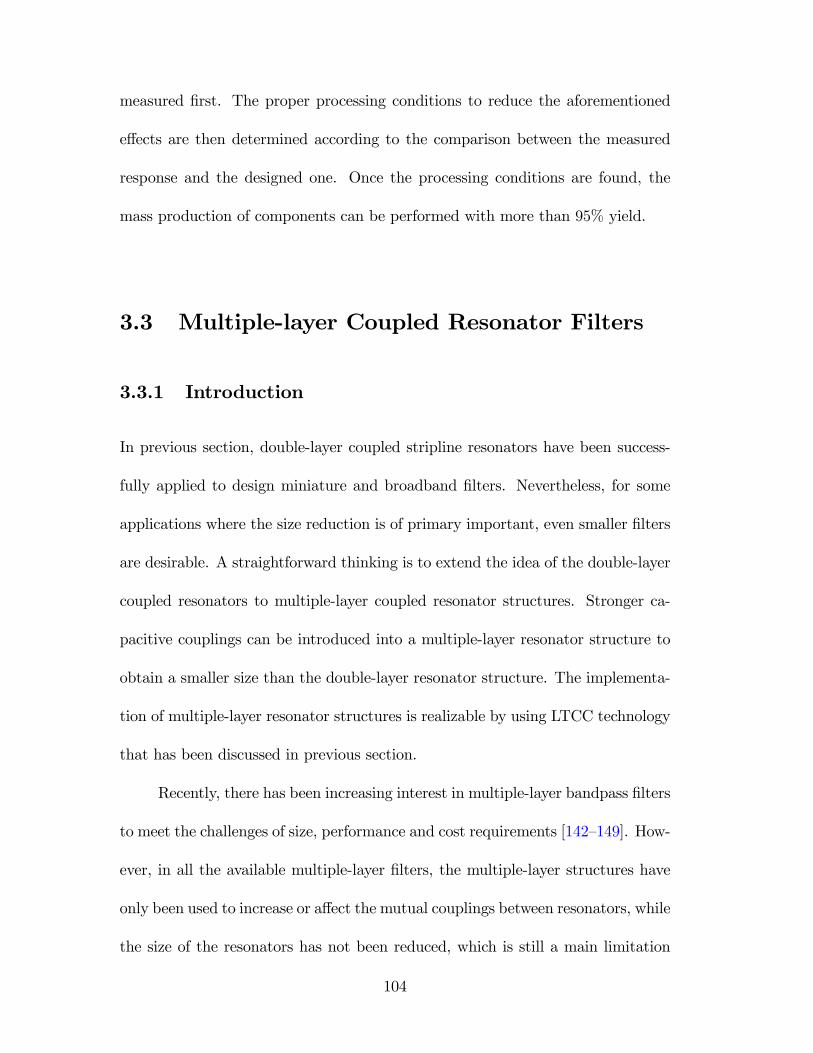
measured �rst. The proper processing conditions to reduce the aforementioned
e¤ects are then determined according to the comparison between the measured
response and the designed one. Once the processing conditions are found, the
mass production of components can be performed with more than 95% yield.
3.3 Multiple-layer Coupled Resonator Filters
3.3.1 Introduction
In previous section, double-layer coupled stripline resonators have been success-
fully applied to design miniature and broadband �lters. Nevertheless, for some
applications where the size reduction is of primary important, even smaller �lters
are desirable. A straightforward thinking is to extend the idea of the double-layer
coupled resonators to multiple-layer coupled resonator structures. Stronger ca-
pacitive couplings can be introduced into a multiple-layer resonator structure to
obtain a smaller size than the double-layer resonator structure. The implementa-
tion of multiple-layer resonator structures is realizable by using LTCC technology
that has been discussed in previous section.
Recently, there has been increasing interest in multiple-layer bandpass �lters
to meet the challenges of size, performance and cost requirements [142�149]. How-
ever, in all the available multiple-layer �lters, the multiple-layer structures have
only been used to increase or a¤ect the mutual couplings between resonators, while
the size of the resonators has not been reduced, which is still a main limitation
104

on the whole �lter size. The multiple-layer structure presented in this section is
employed to signi�cantly reduce the resonator size. Meanwhile, strong couplings
between resonators can still be achieved for broadband �lter designs.
In this section, the idea of generalized multiple-layer coupled resonators is
discussed based on the circuit models as well as the full-wall numerical meth-
ods. Several possible multiple-layer resonator structures are presented, and two
bandpass �lter design examples using such structures are performed to validate
the concept. Commercial software tool Sonnet [72], which is based on MoM, is
employed to do the analysis and design in this section.
3.3.2 Possible Resonator Structures
Shown in Fig. 3.23 are some possible multiple-layer coupled resonator structures.
Fig. 3.23(a) shows double- and triple-layer coupled stripline resonators. Each strip
is grounded at one end and open at the other end. The ground ends of two near
strips are placed at opposite sides to create potential di¤erence along the lines,
and thus, a strong capacitive coupling between them. Fig. 3.23(b), (c) and (d)
are double- and triple-layer coupled hairpin, folded stripline, and spiral resonators,
respectively. Actually almost all the one-layer planar resonator structures can be
extended to multiple-layer coupled resonator structures. The main idea is to create
large potential di¤erences, which leads to strong capacitive couplings, between any
two near one-layer structures inside the resonator. The coupling e¤ects will then
decrease the frequency value of the fundamental resonant mode. From the other
105
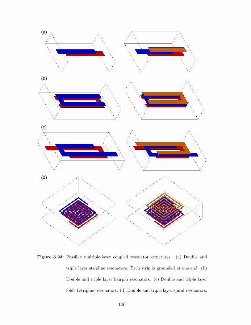
(a)
(b)
(c)
(d)
Figure 3.23: Possible multiple-layer coupled resonator structures. (a) Double and
triple layer stripline resonators. Each strip is grounded at one end. (b)
Double and triple layer hairpin resonators. (c) Double and triple layer
folded stripline resonators. (d) Double and triple layer spiral resonators.
106

point of view, the multiple-layer coupled resonators have shrunk size to realize a
given resonant frequency point due to the capacitive couplings.
The straightforward intuition about the multiple-layer coupled resonators
is that the more number of layers is used, the smaller the resonator size will be
obtained. In order to know whether this intuition makes sense, three stripline
resonators with di¤erent number of layers are analyzed in Sonnet to make com-
parisons. The structures are shown in Fig. 3.24, which are One-layer stripline res-
onator, double-layer coupled stripling resonator, and triple-layer coupled stripline
resonator. They have identical substrate (material and height), identical enclosure
box, and identical strip length. The double- and triple-layer resonators have the
same overlap (coupled) length between two near strips. To decide the resonant
frequency of each structure numerically, two ports are very weakly coupled to the
resonator to excite the fundamental resonant mode (as shown in the geometry
drawings of Fig. 3.24). The simulated S21 response is also shown in Fig. 3.24
for each resonator. The peak frequency points of the S21 responses correspond to
the resonant frequency of each structure, which are 2.672 GHz, 1.383 GHz, and
1.123 GHz for one-layer, double-layer, and triple-layer resonator, respectively. Ac-
cording to the obtained result, it can be concluded that the resonant frequency of
resonator is becoming smaller with the more number of coupled layers (assuming
other dimensions are identical). It also veri�es that the aforementioned intuition
is correct.
The characteristics of multiple-layer coupled resonators can be summarized
as: i) All the available one-layer planar resonator structures can be extended
107
2.4 2.5 2.6 2.7 2.8 2.950
40
30
20
10
0X: 2.672Y: 0.04779
Freq (GHz)
Mag
(dB
)
S21
2.4 2.5 2.6 2.7 2.8 2.950
40
30
20
10
0X: 2.672Y: 0.04779
Freq (GHz)
Mag
(dB
)
S21
1.3 1.35 1.4 1.45 1.5100
80
60
40
20
0X: 1.383Y: 17.6
Freq (GHz)
Mag
(dB
)S21
1.3 1.35 1.4 1.45 1.5100
80
60
40
20
0X: 1.383Y: 17.6
Freq (GHz)
Mag
(dB
)S21
1.1 1.11 1.12 1.13 1.14 1.15100
80
60
40
20
0
X: 1.123Y: 20.19
Freq (GHz)
Mag
(dB
)
S21
1.1 1.11 1.12 1.13 1.14 1.15100
80
60
40
20
0
X: 1.123Y: 20.19
Freq (GHz)
Mag
(dB
)
S21
(a)
(b)
(c)
Figure 3.24: Comparison between resonators with di¤erent number of layers. (a) One-
layer stripline resonator. (b) Double-layer coupled stripline resonator.
(c) Triple-layer coupled stripline resonator.
108
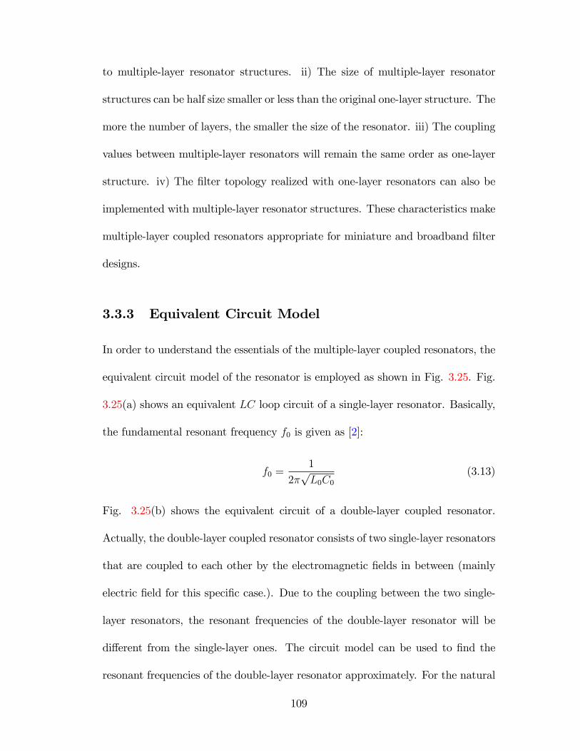
to multiple-layer resonator structures. ii) The size of multiple-layer resonator
structures can be half size smaller or less than the original one-layer structure. The
more the number of layers, the smaller the size of the resonator. iii) The coupling
values between multiple-layer resonators will remain the same order as one-layer
structure. iv) The �lter topology realized with one-layer resonators can also be
implemented with multiple-layer resonator structures. These characteristics make
multiple-layer coupled resonators appropriate for miniature and broadband �lter
designs.
3.3.3 Equivalent Circuit Model
In order to understand the essentials of the multiple-layer coupled resonators, the
equivalent circuit model of the resonator is employed as shown in Fig. 3.25. Fig.
3.25(a) shows an equivalent LC loop circuit of a single-layer resonator. Basically,
the fundamental resonant frequency f0 is given as [2]:
f0 =1
2�pL0C0
(3.13)
Fig. 3.25(b) shows the equivalent circuit of a double-layer coupled resonator.
Actually, the double-layer coupled resonator consists of two single-layer resonators
that are coupled to each other by the electromagnetic �elds in between (mainly
electric �eld for this speci�c case.). Due to the coupling between the two single-
layer resonators, the resonant frequencies of the double-layer resonator will be
di¤erent from the single-layer ones. The circuit model can be used to �nd the
resonant frequencies of the double-layer resonator approximately. For the natural
109
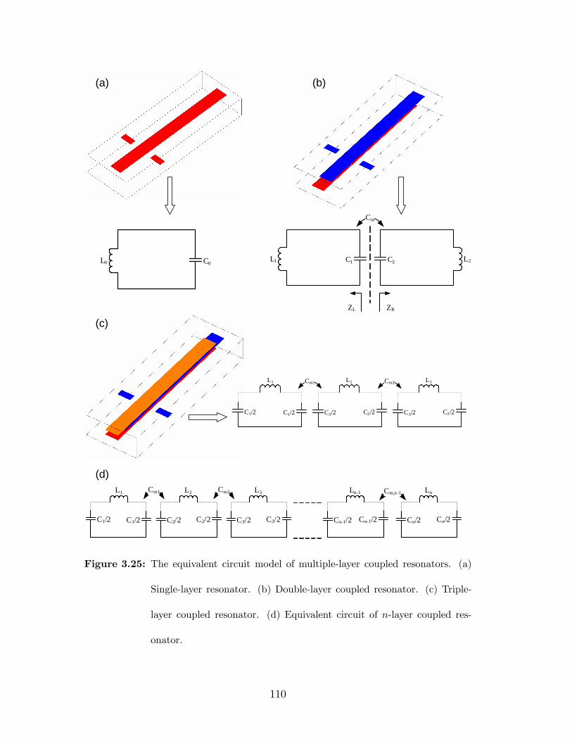
(a) (b)
(c)
L1 C1 L2C2
Cm
ZL ZR
L0 C0
C1/2
L1
C1/2 C2/2
L2
C2/2
Cm1
C3/2
L3
C3/2
Cm2
(d)
C1/2
L1
C1/2 C2/2
L2
C2/2
Cm1
C3/2
L3
C3/2
Cm2
Cn1/2
Ln1
Cn1/2 Cn/2
Ln
Cn/2
Cm,n1
Figure 3.25: The equivalent circuit model of multiple-layer coupled resonators. (a)
Single-layer resonator. (b) Double-layer coupled resonator. (c) Triple-
layer coupled resonator. (d) Equivalent circuit of n-layer coupled res-
onator.
110

resonance of the circuit model in Fig. 3.25(b), the condition is
ZL = �ZR (3.14)
where ZL and ZR are the input impedances looking at the left and the right
of the reference plane (dotted line in Fig. 3.25(b)). This condition leads to an
eigen-equation
!4�L1L2C1C2 � L1L2C2m
�� !2 (L1C1 + L2C2) + 1 = 0 (3.15)
The resonant frequencies can, therefore, be solved as
f1;2 =
vuutf 201 + f 202 �q(f 202 � f 201)
2+ 4f 201f
202k
2
2 (1� k2) (3.16)
where f01 and f02 are the unloaded resonant frequency of the two single-layer
resonators, respectively. They are given by f0i = 12�pLiCi
, i = 1; 2. k is the
normalized coupling given by
k2 =C2mC1C2
(3.17)
Usually the resonant frequencies of the two single-layer resonators are iden-
tical, i.e. f01 = f02 = f0. Therefore, the two natural resonant frequencies of the
double-layer resonator are
f1 =f0p1 + k
and f2 =f0p1� k
(3.18)
Thus, if the coupling between two single-layer resonators is very strong, i.e. k is
large, f1 will be much smaller than f0 and f2 much larger than f0. The fundamen-
tal resonant mode f1 can then be used for �lter designs to achieve a miniature size
111
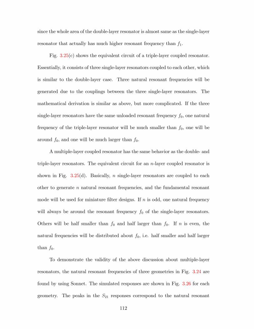
since the whole area of the double-layer resonator is almost same as the single-layer
resonator that actually has much higher resonant frequency than f1.
Fig. 3.25(c) shows the equivalent circuit of a triple-layer coupled resonator.
Essentially, it consists of three single-layer resonators coupled to each other, which
is similar to the double-layer case. Three natural resonant frequencies will be
generated due to the couplings between the three single-layer resonators. The
mathematical derivation is similar as above, but more complicated. If the three
single-layer resonators have the same unloaded resonant frequency f0, one natural
frequency of the triple-layer resonator will be much smaller than f0, one will be
around f0, and one will be much larger than f0.
A multiple-layer coupled resonator has the same behavior as the double- and
triple-layer resonators. The equivalent circuit for an n-layer coupled resonator is
shown in Fig. 3.25(d). Basically, n single-layer resonators are coupled to each
other to generate n natural resonant frequencies, and the fundamental resonant
mode will be used for miniature �lter designs. If n is odd, one natural frequency
will always be around the resonant frequency f0 of the single-layer resonators.
Others will be half smaller than f0 and half larger than f0. If n is even, the
natural frequencies will be distributed about f0, i.e. half smaller and half larger
than f0.
To demonstrate the validity of the above discussion about multiple-layer
resonators, the natural resonant frequencies of three geometries in Fig. 3.24 are
found by using Sonnet. The simulated responses are shown in Fig. 3.26 for each
geometry. The peaks in the S21 responses correspond to the natural resonant
112
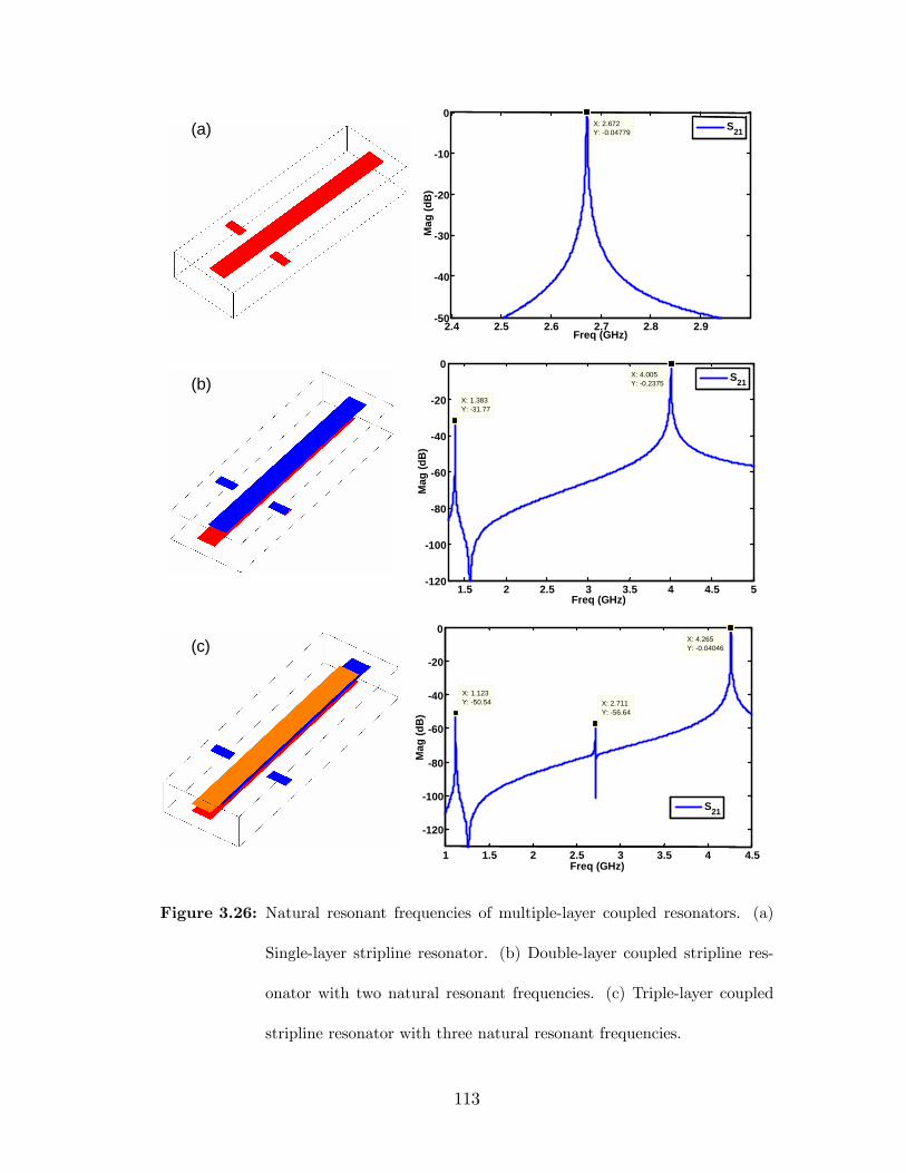
2.4 2.5 2.6 2.7 2.8 2.950
40
30
20
10
0X: 2.672Y: 0.04779
Freq (GHz)
Mag
(dB
)
S21
2.4 2.5 2.6 2.7 2.8 2.950
40
30
20
10
0X: 2.672Y: 0.04779
Freq (GHz)
Mag
(dB
)
S21(a)
(b)
(c)
1.5 2 2.5 3 3.5 4 4.5 5120
100
80
60
40
20
0
X: 1.383Y: 31.77
Freq (GHz)
Mag
(dB
)
X: 4.005Y: 0.2375
S21
1.5 2 2.5 3 3.5 4 4.5 5120
100
80
60
40
20
0
X: 1.383Y: 31.77
Freq (GHz)
Mag
(dB
)
X: 4.005Y: 0.2375
S21
1 1.5 2 2.5 3 3.5 4 4.5
120
100
80
60
40
20
0
X: 1.123Y: 50.54
Freq (GHz)
Mag
(dB
)
X: 2.711Y: 56.64
X: 4.265Y: 0.04046
S21
1 1.5 2 2.5 3 3.5 4 4.5
120
100
80
60
40
20
0
X: 1.123Y: 50.54
Freq (GHz)
Mag
(dB
)
X: 2.711Y: 56.64
X: 4.265Y: 0.04046
S21
Figure 3.26: Natural resonant frequencies of multiple-layer coupled resonators. (a)
Single-layer stripline resonator. (b) Double-layer coupled stripline res-
onator with two natural resonant frequencies. (c) Triple-layer coupled
stripline resonator with three natural resonant frequencies.
113
frequencies of the resonators. The values are: 2.672 GHz for the single-layer
resonator, 1.383 GHz and 4.005 GHz for the double-layer resonator, and 1.123
GHz, 2.711 GHz, and 4.265 GHz for the triple-layer resonator. These found values
are consistent with the above essential discussions of multiple-layer resonators.
For a given center frequency of a �lter design, the more number of layers
is used in a multiple-layer coupled resonator, the smaller resonator size can be
obtained. However, the spurious performance will be becoming worse with the
more number of layers because the second resonant mode will be closer to the
fundamental resonant mode. It can be seen from Fig. 3.26(b) and (c): the triple-
layer stripline resonator has a second resonant mode at 2.711 GHz, while the
double-layer resonator has one at 4.005 GHz.
3.3.4 Filter Con�guration
Many �lter con�gurations can be realized by multiple-layer coupled resonators.
The most commonly used ones are the so-called combline and interdigital con�g-
urations (as shown in Fig. 3.7 using double-layer resonators). They are extended
structures from the single-layer combline and interdigital �lters. In the multiple-
layer �lter structures, the strips ( or single-layer structures) of one resonator are
coupled to the strips at the same layer of another resonator. Therefore, the inter-
coupling between two resonators is the combined couplings between the paired
strips at each layer. The strong inter-coupling values are, thus, still achievable
between the multiple-layer coupled resonators even though the size (area) of the
114
resonators is compact. Therefore, multiple-layer coupled resonators are appropri-
ate for miniature and broadband �lter designs.
Actually, other quasi-elliptic �lter con�gurations realized by single-layer res-
onators are also able to be implemented by multiple-layer coupled resonators.
However, the �lter structures will be more complicated, which also makes the
analysis and design more di¢ cult. Mode matching method used in previous sec-
tion for double-layer resonator �lters might not be an appropriate tool to analyze
some multiple-layer resonator structures. FEM (in Ansoft HFSS) and MoM (in
Sonnet) can, thus, be employed to perform the analysis and design. A systematic
design methodology is then necessary to compensate the low e¢ ciency of FEM
and MoM. Two examples using MoM in Sonnet are given next to illustrate the
design procedure.
In practice, three main factors are usually considered to decide the number of
layers used in a resonator: �lter size, �lter bandwidth, and spurious performance.
Generally, with the more number of layers, the �lter size will be smaller, achievable
bandwidth will be narrower, and the spurious performance will be worse.
3.3.5 Triple-layer Coupled Stripline Resonator Filter
To demonstrate the feasibility of the multiple-layer coupled resonator �lters, a
design of six-order Chebyshev �lter using triple-layer coupled stripline resonators
is performed. The bandwidth is from 1.0 GHz to 1.27 GHz (~23% relative band-
width). The return loss should be better than 18 dB in-band. The required
115
couplings are
Rin = Rout = 1:10643 (276:61 MHz)
M12 = M56 = 0:88859 (222:15 MHz)
M23 = M45 = 0:62816 (157:04 MHz)
M34 = 0:59653 (149:13 MHz) (3.19)
The coupling values in MHz are the actual couplings used in the design process,
which are obtained by multiplying the normalized coupling values by the �lter
bandwidth. An interdigital con�guration is employed to ful�ll the �lter (as shown
in Fig. 3.30(a)). LTCC technology will be used to manufacture the �lter. The
LTCC parameters are: relative permittivity of ceramics "r = 5:9, thickness of
metallization ts = 0:4mil, and thickness of each ceramic layer tc = 3:74mil.
The triple-layer coupled stripline resonator structure is shown in Fig. 3.27(a).
The vertical dimensions are decided according to the desired stack option in
LTCC. The heights of the three metallization layers as shown in Fig. 3.27(b)
are: h1 = 29:68mil, h2 = 37: 08mil, and h3 = 44: 48mil, respectively. The height
of the box is h = 63: 02mil. The length lr of the box or resonator as shown in
Fig. 3.27(c) is taken as a �xed value 480mil. The width ws of each strip in the
resonator is also �xed at 40mil. Three strips in the resonator have the identical
length ls. The center frequency of the �lter is about 1.135 GHz. In order to
obtain a resonator resonating at 1.135 GHz, the strip length ls is swept to �nd
the right value. Basically, the resonator is weakly excited at the middle layer by
two striplines. The S21 response is simulated in Sonnet to search for the resonant
116
lr
ls ws
lr
ls ws
h1 h2 h3
h
h1 h2 h3
h
(a) (b)
(c)
1.1 1.11 1.12 1.13 1.14 1.15100
80
60
40
20
0
Freq (GHz)
Mag
(dB
)
S21
1.1 1.11 1.12 1.13 1.14 1.15100
80
60
40
20
0
Freq (GHz)
Mag
(dB
)
S21
(d)
Figure 3.27: A triple-layer coupled stripline resonator (Drawings are not in scale). (a)
3D view with excitations. (b) End view. (c) Side view. (d) Typical S21
response.117

frequency. A typical S21 response is shown in Fig. 3.27(d). The �nally decided
value of ls is 444mil.
The external input and output couplings are provided by tapped-in 50-ohm
striplines as shown in Fig. 3.28(a). The 50-ohm stripline can be tapped onto any
of the three strips in one resonator. In this speci�c case, the middle strip of the
resonator is used. A loop is constructed by the 50-ohm stripline and the middle
strip of the resonator, which mainly provides the magnetic coupling to excite the
resonator. Therefore, the larger the tapped-in position htap, the stronger the
external coupling (because the loop is larger). The dimension htap is swept to
calculate the external coupling values by using (3.7). The obtained coupling curves
are shown in Fig. 3.28(b): coupling value R vs htap, and the loaded frequency f0
vs htap. It can be seen that R is linearly proportional to htap and f0 is almost
constant. For this design, R should be about 276.61 MHz, and f0 should be
around 1.135 GHz. The value htap found by interpolation is about 368mil.
The inter-coupling structure is shown in Fig. 3.29(a), which is an interdigital
con�guration. The separation s between two resonators is swept to compute the
coupling values and the loaded frequencies. The formulation (3.4) is used to
calculate the coupling value M , while the loaded frequency is given by
f0 =
s2f 21 f
22
f 21 + f 22�pf1f2 (3.20)
where f1 and f2 are the two peak frequency points of the simulated S21 response
of the structure in Fig. 3.29(a). The obtained coupling curves are shown in
Fig. 3.29(b): inter-coupling value M vs s and f0 vs s. The values of s found
118
340 345 350 355 360 365 370 375 380240
260
280
R (M
Hz)
htap (mil)
340 345 350 355 360 365 370 375 3801.13
1.135
1.14
htap (mil)
f 0(G
Hz)
340 345 350 355 360 365 370 375 380240
260
280
R (M
Hz)
htap (mil)
340 345 350 355 360 365 370 375 3801.13
1.135
1.14
htap (mil)
f 0(G
Hz)
(a)
(b)
htaphtap
Figure 3.28: External coupling structure and computed coupling curves. (a) Tapped-
in stripline external coupling structure. (b) External coupling curves
with respect to the tapped-in position htap.
119
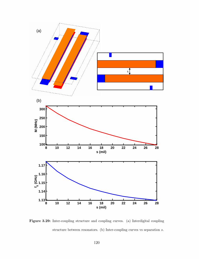
s
8 10 12 14 16 18 20 22 24 26 28100
150
200
250
300
s (mil)
M (M
Hz)
8 10 12 14 16 18 20 22 24 26 281.13
1.14
1.15
1.16
1.17
s (mil)
f 0(G
Hz)
8 10 12 14 16 18 20 22 24 26 28100
150
200
250
300
s (mil)
M (M
Hz)
8 10 12 14 16 18 20 22 24 26 281.13
1.14
1.15
1.16
1.17
s (mil)
f 0(G
Hz)
(a)
(b)
Figure 3.29: Inter-coupling structure and coupling curves. (a) Interdigital coupling
structure between resonators. (b) Inter-coupling curves vs separation s.
120

by interpolation to provide the desired inter-couplings M12, M23, and M34 are
s1 = 13:3mil, s2 = 19:2mil, and s3 = 20:1mil (variables are de�ned in Fig.
3.30(b)), respectively. The loaded frequencies with respect to s1, s2, and s3 are
1.151 GHz, 1.138 GHz, and 1.136 GHz. These frequency values will be helpful for
later tuning procedure.
The whole �lter structure is assembled according to the obtained initial
dimensions. Shown in Fig. 3.30 are the 3D and top views of the �lter structure.
The frequency response of this �lter is simulated in Sonnet. It is well-known that
uniform cells are used in Sonnet to perform the simulation. Therefore, in order to
improve the simulation e¢ ciency, integer values are taken for all the dimensions
(Larger cells can, thus, be used in Sonnet). The used values of s1, s2, and s3 are
13, 19, and 20, respectively. The simulated response of the initial �lter structure
is shown in Fig. 3.31, which is a very good starting point for further tuning or
optimization. The simulation time for this structure is about 18 minutes in a
desktop PC with 3.0 GHz Pentium 4 CPU and 4 GB memory.
The �lter dimensions need to be tuned or optimized to satisfy the require-
ments. The optimization speed is not acceptable since about 18 minutes are
required for one single iteration. However, it is possible to tune the dimensions ac-
cording to the calculated coupling curves, especially the loaded frequency curves.
The loaded frequencies of the �rst and the second resonators are about 1.151
GHz, which is higher than the desired center frequency. The widths of these two
resonators can be increased to tune the frequency down. The tuning step for
all the dimensions is taken as 1 or 2 mil to keep the simulation e¢ ciency. The
121
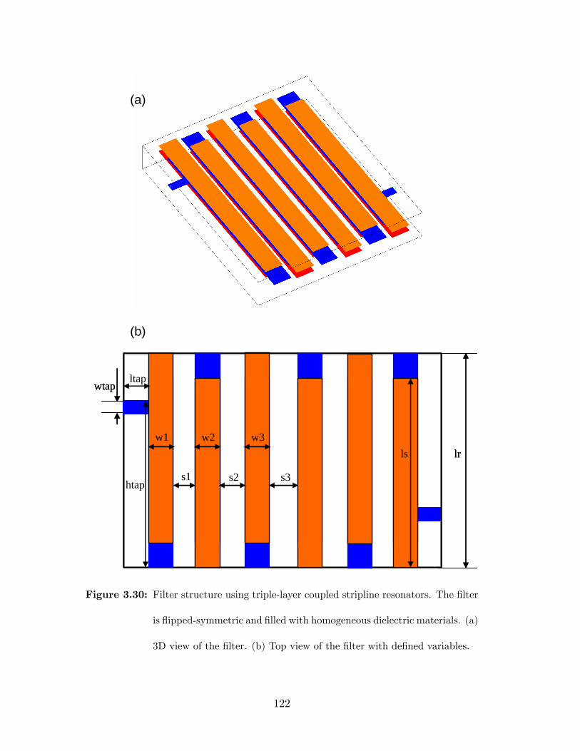
htap
wtapltap
w1 w2 w3
s1 s2 s3
lrls
htap
wtapltap
w1 w2 w3
s1 s2 s3
lrls
(a)
(b)
Figure 3.30: Filter structure using triple-layer coupled stripline resonators. The �lter
is �ipped-symmetric and �lled with homogeneous dielectric materials. (a)
3D view of the �lter. (b) Top view of the �lter with de�ned variables.
122
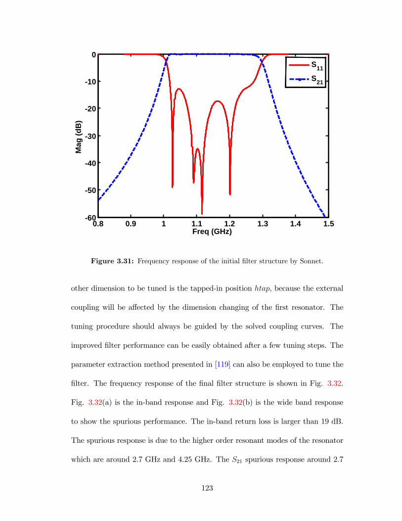
0.8 0.9 1 1.1 1.2 1.3 1.4 1.560
50
40
30
20
10
0
Freq (GHz)
Mag
(dB
)
S11
S21
0.8 0.9 1 1.1 1.2 1.3 1.4 1.560
50
40
30
20
10
0
Freq (GHz)
Mag
(dB
)
S11
S21
Figure 3.31: Frequency response of the initial �lter structure by Sonnet.
other dimension to be tuned is the tapped-in position htap, because the external
coupling will be a¤ected by the dimension changing of the �rst resonator. The
tuning procedure should always be guided by the solved coupling curves. The
improved �lter performance can be easily obtained after a few tuning steps. The
parameter extraction method presented in [119] can also be employed to tune the
�lter. The frequency response of the �nal �lter structure is shown in Fig. 3.32.
Fig. 3.32(a) is the in-band response and Fig. 3.32(b) is the wide band response
to show the spurious performance. The in-band return loss is larger than 19 dB.
The spurious response is due to the higher order resonant modes of the resonator
which are around 2.7 GHz and 4.25 GHz. The S21 spurious response around 2.7
123
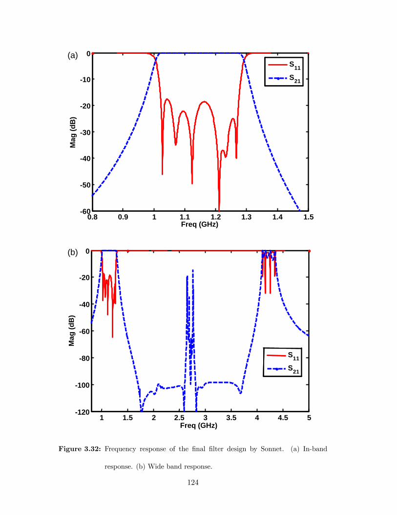
0.8 0.9 1 1.1 1.2 1.3 1.4 1.560
50
40
30
20
10
0
Freq (GHz)
Mag
(dB
)S11
S21
0.8 0.9 1 1.1 1.2 1.3 1.4 1.560
50
40
30
20
10
0
Freq (GHz)
Mag
(dB
)S11
S21
1 1.5 2 2.5 3 3.5 4 4.5 5120
100
80
60
40
20
0
Freq (GHz)
Mag
(dB
)
S11
S21
1 1.5 2 2.5 3 3.5 4 4.5 5120
100
80
60
40
20
0
Freq (GHz)
Mag
(dB
)
S11
S21
(a)
(b)
Figure 3.32: Frequency response of the �nal �lter design by Sonnet. (a) In-band
response. (b) Wide band response.
124
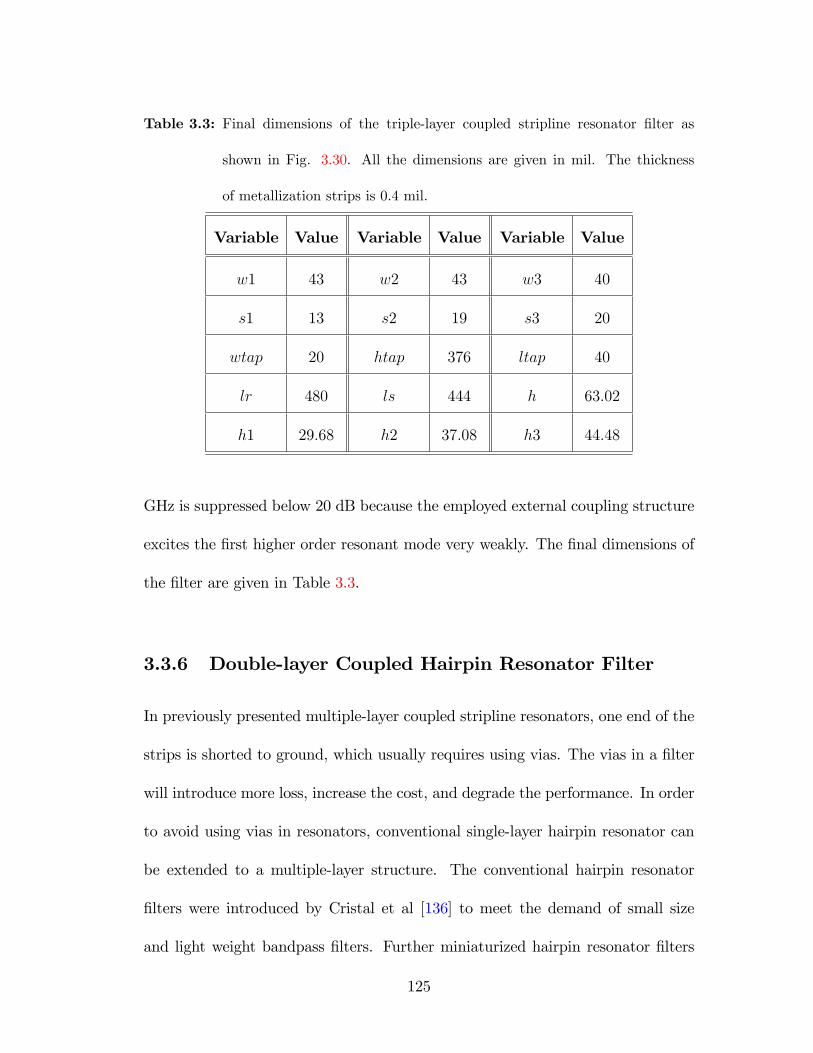
Table 3.3: Final dimensions of the triple-layer coupled stripline resonator �lter as
shown in Fig. 3.30. All the dimensions are given in mil. The thickness
of metallization strips is 0.4 mil.
Variable Value Variable Value Variable Value
w1 43 w2 43 w3 40
s1 13 s2 19 s3 20
wtap 20 htap 376 ltap 40
lr 480 ls 444 h 63:02
h1 29:68 h2 37:08 h3 44:48
GHz is suppressed below 20 dB because the employed external coupling structure
excites the �rst higher order resonant mode very weakly. The �nal dimensions of
the �lter are given in Table 3.3.
3.3.6 Double-layer Coupled Hairpin Resonator Filter
In previously presented multiple-layer coupled stripline resonators, one end of the
strips is shorted to ground, which usually requires using vias. The vias in a �lter
will introduce more loss, increase the cost, and degrade the performance. In order
to avoid using vias in resonators, conventional single-layer hairpin resonator can
be extended to a multiple-layer structure. The conventional hairpin resonator
�lters were introduced by Cristal et al [136] to meet the demand of small size
and light weight bandpass �lters. Further miniaturized hairpin resonator �lters
125
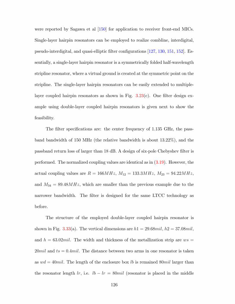
were reported by Sagawa et al [150] for application to receiver front-end MICs.
Single-layer hairpin resonators can be employed to realize combline, interdigital,
pseudo-interdigital, and quasi-elliptic �lter con�gurations [127, 130, 151, 152]. Es-
sentially, a single-layer hairpin resonator is a symmetrically folded half-wavelength
stripline resonator, where a virtual ground is created at the symmetric point on the
stripline. The single-layer hairpin resonators can be easily extended to multiple-
layer coupled hairpin resonators as shown in Fig. 3.23(c). One �lter design ex-
ample using double-layer coupled hairpin resonators is given next to show the
feasibility.
The �lter speci�cations are: the center frequency of 1.135 GHz, the pass-
band bandwidth of 150 MHz (the relative bandwidth is about 13.22%), and the
passband return loss of larger than 18 dB. A design of six-pole Chebyshev �lter is
performed. The normalized coupling values are identical as in (3.19). However, the
actual coupling values are R = 166MHz, M12 = 133:3MHz, M23 = 94:22MHz,
and M34 = 89:48MHz, which are smaller than the previous example due to the
narrower bandwidth. The �lter is designed for the same LTCC technology as
before.
The structure of the employed double-layer coupled hairpin resonator is
shown in Fig. 3.33(a). The vertical dimensions are h1 = 29:68mil, h2 = 37:08mil,
and h = 63:02mil. The width and thickness of the metallization strip are ws =
20mil and ts = 0:4mil. The distance between two arms in one resonator is taken
as wd = 40mil. The length of the enclosure box lb is remained 80mil larger than
the resonator length lr, i.e. lb � lr = 80mil (resonator is placed in the middle
126
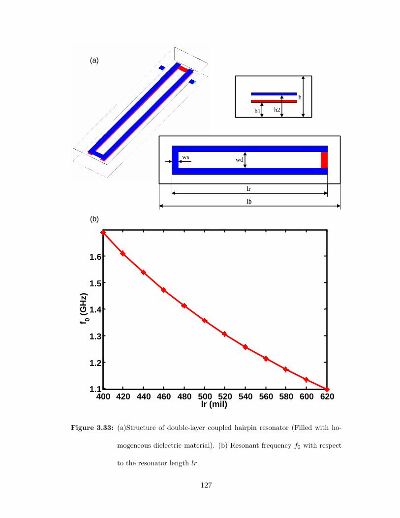
h1 h2
h
h1 h2
h
wdws
lr
lb
wdws
lr
lb
400 420 440 460 480 500 520 540 560 580 600 6201.1
1.2
1.3
1.4
1.5
1.6
lr (mil)
f 0(G
Hz)
400 420 440 460 480 500 520 540 560 580 600 6201.1
1.2
1.3
1.4
1.5
1.6
lr (mil)
f 0(G
Hz)
(a)
(b)
Figure 3.33: (a)Structure of double-layer coupled hairpin resonator (Filled with ho-
mogeneous dielectric material). (b) Resonant frequency f0 with respect
to the resonator length lr.
127

of the box). The resonator length lr is swept to search for the desired resonant
frequency of 1.135 GHz. Shown in Fig. 3.33(b) is the calculated curve of the
resonant frequency f0 with respect to the resonator length lr. The value of lr is
found to be 604mil by interpolation.
External couplings are also realized by tapped-in 50-ohm striplines as in
previous examples. The tapped-in position htap is swept to calculate the external
coupling value R and the loaded resonant frequency f0. The obtained coupling
curves are shown in Fig. 3.34(a). To have a coupling value R = 166MHz, htap
is found to be 428mil. However, the loaded resonant frequency f0 is about 1.084
GHz that is smaller than the desired value of 1.135 GHz. The dimension wd is,
therefore, decreased to increase the loaded resonant frequency f0 and, meanwhile,
remain the external coupling value R. The value of wd is taken as 28mil �nally.
Two resonators are interdigitally coupled to each other as shown in the inset
of Fig. 3.34(b). The calculation of inter-coupling value M and loaded frequency
f0 is following the same method presented before. The coupling curves are shown
in Fig. 3.34(b). The values of the separation s for providing the desired inter-
couplings are s1 = 10:8mil, s2 = 16:4mil, and s3 = 17:3mil (variables de�ned in
Fig. 3.35(a)). The loaded resonant frequencies are 1.135 GHz, 1.131 GHz, and
1.130 GHz, respectively.
The assembled �lter structure is shown in Fig. 3.35(a). The initial dimen-
sions are taken with the resolution of 0:5mil to gain the acceptable simulation
speed in Sonnet. The used values of s1, s2, and s3 are 10.5, 16.5, and 17.5, re-
spectively. The frequency response of the initial �lter is shown in Fig. 3.35(b),
128
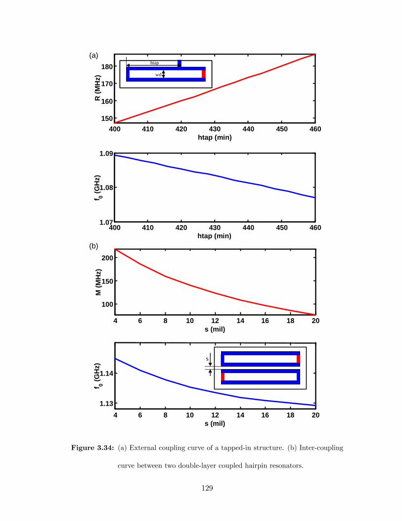
400 410 420 430 440 450 460150
160
170
180
htap (min)
R (M
Hz)
400 410 420 430 440 450 4601.07
1.08
1.09
htap (min)
f 0(G
Hz)
400 410 420 430 440 450 460150
160
170
180
htap (min)
R (M
Hz)
400 410 420 430 440 450 4601.07
1.08
1.09
htap (min)
f 0(G
Hz)
wd
htap
4 6 8 10 12 14 16 18 201.13
1.14
s (mil)
f 0(G
Hz)
4 6 8 10 12 14 16 18 20
100
150
200
s (mil)
M (M
Hz)
s
4 6 8 10 12 14 16 18 201.13
1.14
s (mil)
f 0(G
Hz)
4 6 8 10 12 14 16 18 20
100
150
200
s (mil)
M (M
Hz)
4 6 8 10 12 14 16 18 201.13
1.14
s (mil)
f 0(G
Hz)
4 6 8 10 12 14 16 18 20
100
150
200
s (mil)
M (M
Hz)
s
(a)
(b)
Figure 3.34: (a) External coupling curve of a tapped-in structure. (b) Inter-coupling
curve between two double-layer coupled hairpin resonators.
129
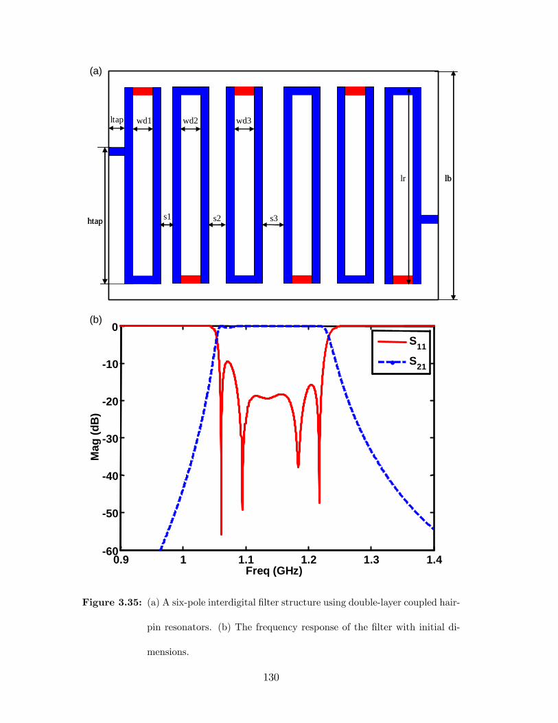
ltap wd1 wd2 wd3
s1 s2 s3htap
lblr
ltap wd1 wd2 wd3
s1 s2 s3htap
lblr
0.9 1 1.1 1.2 1.3 1.460
50
40
30
20
10
0
Freq (GHz)
Mag
(dB
)
S11
S21
0.9 1 1.1 1.2 1.3 1.460
50
40
30
20
10
0
Freq (GHz)
Mag
(dB
)
S11
S21
(a)
(b)
Figure 3.35: (a) A six-pole interdigital �lter structure using double-layer coupled hair-
pin resonators. (b) The frequency response of the �lter with initial di-
mensions.
130
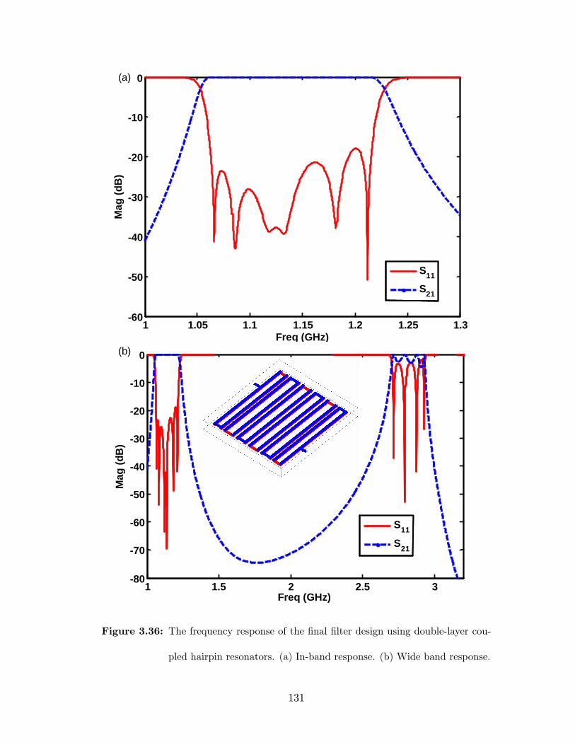
1 1.05 1.1 1.15 1.2 1.25 1.360
50
40
30
20
10
0
Freq (GHz)
Mag
(dB
)
S11
S21
1 1.05 1.1 1.15 1.2 1.25 1.360
50
40
30
20
10
0
Freq (GHz)
Mag
(dB
)
S11
S21
1 1.5 2 2.5 380
70
60
50
40
30
20
10
0
Freq (GHz)
Mag
(dB
)
S11
S21
1 1.5 2 2.5 380
70
60
50
40
30
20
10
0
Freq (GHz)
Mag
(dB
)
S11
S21
1 1.5 2 2.5 380
70
60
50
40
30
20
10
0
Freq (GHz)
Mag
(dB
)
S11
S21
(a)
(b)
Figure 3.36: The frequency response of the �nal �lter design using double-layer cou-
pled hairpin resonators. (a) In-band response. (b) Wide band response.
131
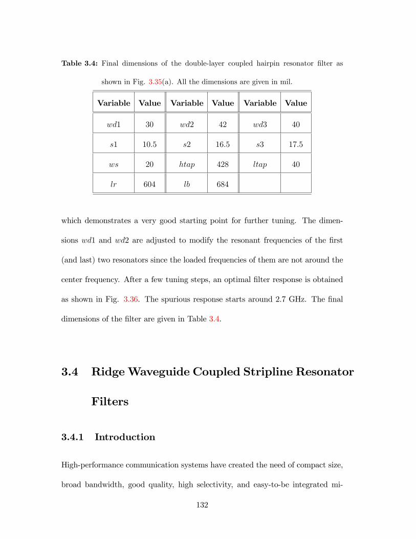
Table 3.4: Final dimensions of the double-layer coupled hairpin resonator �lter as
shown in Fig. 3.35(a). All the dimensions are given in mil.
Variable Value Variable Value Variable Value
wd1 30 wd2 42 wd3 40
s1 10:5 s2 16:5 s3 17:5
ws 20 htap 428 ltap 40
lr 604 lb 684
which demonstrates a very good starting point for further tuning. The dimen-
sions wd1 and wd2 are adjusted to modify the resonant frequencies of the �rst
(and last) two resonators since the loaded frequencies of them are not around the
center frequency. After a few tuning steps, an optimal �lter response is obtained
as shown in Fig. 3.36. The spurious response starts around 2.7 GHz. The �nal
dimensions of the �lter are given in Table 3.4.
3.4 RidgeWaveguide Coupled Stripline Resonator
Filters
3.4.1 Introduction
High-performance communication systems have created the need of compact size,
broad bandwidth, good quality, high selectivity, and easy-to-be integrated mi-
132
crowave �lters and multiplexers. Planar �lters are currently popular structures
in integrated PCB circuits because of their small size and lower fabrication cost.
The drawback of planar �lters is the relatively-low quality factor. Waveguide
�lters are recently applied in PCB circuits using LTCC technology for achieving
higher quality factors. They are manufactured as multiple-layer structures to have
high-integration level. LTCC ridge waveguide �lter and multiplexer designs were
presented in [61, 62, 141, 153]. The drawback of LTCC ridge waveguide �lters is
their relatively-large cross sections, especially their heights. Many ceramic layers
are usually required to implement the ridge waveguide �lters in LTCC technol-
ogy, which will increase the cost and degrade the �lter performance because the
variation of the dielectric permittivity is increased with the number of ceramic
layers. Therefore, new �lter structures with more compact cross sections than
ridge waveguides and better quality than planar structures need to be found for
some integrated circuit systems.
The size of waveguide �lters is mainly constrained by the cut-o¤ frequency
of their fundamental TE/TM mode, while planar �lters do not have such con-
straint because TEM mode is their main operating mode (the size of planar �lters
is usually constrained by the resonator structures and the coupling mechanism).
The idea is to use a TEM-mode resonator structure to gain a smaller �lter cross
section than other waveguide ones. New �lter con�gurations using stripline res-
onators are presented in this section. The stripline resonators are coupled by
ridge waveguide evanescent-mode sections to ful�ll a bandpass �lter and main-
tain the in-line topology (�lter cross section remains same). The cross section of
133
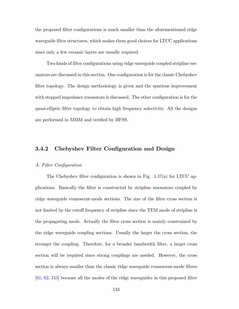
the proposed �lter con�gurations is much smaller than the aforementioned ridge
waveguide �lter structures, which makes them good choices for LTCC applications
since only a few ceramic layers are usually required.
Two kinds of �lter con�gurations using ridge waveguide coupled stripline res-
onators are discussed in this section. One con�guration is for the classic Chebyshev
�lter topology. The design methodology is given and the spurious improvement
with stepped impedance resonators is discussed. The other con�guration is for the
quasi-elliptic �lter topology to obtain high frequency selectivity. All the designs
are performed in MMM and veri�ed by HFSS.
3.4.2 Chebyshev Filter Con�guration and Design
A. Filter Con�guration
The Chebyshev �lter con�guration is shown in Fig. 3.37(a) for LTCC ap-
plications. Basically the �lter is constructed by stripline resonators coupled by
ridge waveguide evanescent-mode sections. The size of the �lter cross section is
not limited by the cuto¤ frequency of stripline since the TEM mode of stripline is
the propagating mode. Actually the �lter cross section is mainly constrained by
the ridge waveguide coupling sections. Usually the larger the cross section, the
stronger the coupling. Therefore, for a broader bandwidth �lter, a larger cross
section will be required since strong couplings are needed. However, the cross
section is always smaller than the classic ridge waveguide evanescent-mode �lters
[61, 62, 153] because all the modes of the ridge waveguides in this proposed �lter
134
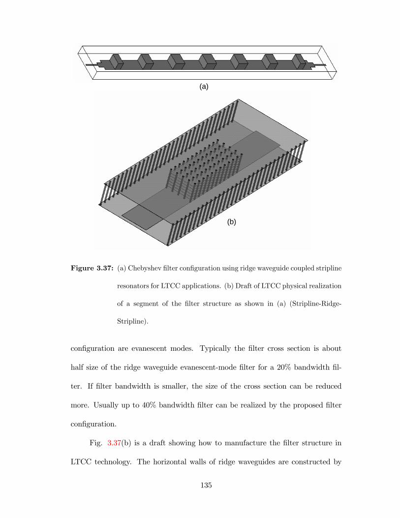
(a)
(b)
Figure 3.37: (a) Chebyshev �lter con�guration using ridge waveguide coupled stripline
resonators for LTCC applications. (b) Draft of LTCC physical realization
of a segment of the �lter structure as shown in (a) (Stripline-Ridge-
Stripline).
con�guration are evanescent modes. Typically the �lter cross section is about
half size of the ridge waveguide evanescent-mode �lter for a 20% bandwidth �l-
ter. If �lter bandwidth is smaller, the size of the cross section can be reduced
more. Usually up to 40% bandwidth �lter can be realized by the proposed �lter
con�guration.
Fig. 3.37(b) is a draft showing how to manufacture the �lter structure in
LTCC technology. The horizontal walls of ridge waveguides are constructed by
135

printing parallel planar conductors, while the vertical walls are realized by closely
spaced metal vias. The stripline is implemented by one metallization layer. Thus,
the �lter can be embedded into multiple layer ceramics and integrated with other
PCB circuits.
B. Filter Modeling in MMM
The full wave analysis of the proposed �lter structure in Fig. 3.37(a) is
carried out by means of rigorous mode matching method. Solid wall structures
without vias are considered at the design stage (The �lter is usually designed with
su¢ cient margin with respect to the speci�cations to compensate the e¤ects of the
vias.). The mode matching analysis consists of three steps as discussed in Subsec.
1.2.3 (p. 11): i) Calculate the eigenmodes of all the involved waveguides. ii)
Characterize each discontinuity by GSM. iii) Compute the complete �lter response
by cascading the GSMs of each discontinuity.
Two types of waveguides appear in the �lter structure of Fig. 3.37(a):
stripline and ridge waveguide. Their cross sections are shown in Fig. 3.38(a).
The eigenmodes of stripline are classi�ed as TEM, TE and TM modes, while the
eigenmodes in ridge waveguide are classi�ed as TE and TM modes. The eigen-
modes of these two waveguides can be solved by the GTR technique discussed in
Appendix A (p. 255). The typical electric �eld distribution of the fundamental
TEM mode of a stripline cross-section is shown in Fig. B.1(a) (p. 269), while the
fundamental TE mode of a single-ridge waveguide is shown in Fig. B.1(c).
Two types of waveguide discontinuities exist in the �lter structure: stripline
to stripline and stripline to ridge waveguide. The GSM of these two types of dis-
136
PMW PMW
(top view) (top view)
(side view) (side view)
(top view) (top view)
(side view) (side view)
(a)
(b) (c)
Figure 3.38: (a) Two types of cross sections that appear in the Chebyshev �lter con-
�guration: Stripline and Ridge waveguide. (b) Stripline tapped-in exci-
tation for the external coupling. (c) Inter-coupling section between two
stripline resonators by evanescent ridge waveguide.
137
continuities can be solved using the �eld matching procedure in Table 1.2 (p. 16).
The coupling integrals X in Table 1.2 can be calculated based on the formulations
in Appendix C (p. 271).
The GSM cascading is performed by using (1.2) to obtain the whole �lter
response. It is important to note that the �lter has symmetry with respect to
the middle plane along the overall length. Therefore, only the eigenmodes with
PMW at the symmetric plane should be considered in the MMM analysis, which
will signi�cantly reduce the simulation time.
C. Filter Design Procedure
To design a �lter with the proposed con�guration as in Fig. 3.37(a), dimen-
sions of the cross sections of stripline and ridge waveguide should be determined
�rst according to the �lter speci�cations, such as center frequency f0 and pass-
band bandwidth. Typically the cuto¤ frequency of the fundamental mode of the
ridge waveguide can be chosen around 2f0 for 15%�20% bandwidth �lters, which
will generate strong enough couplings between stripline resonators.
The �lter design consists of two steps after the cross sections have been de-
termined. The �rst step is to obtain the initial dimensions of the �lter based on
the impedance inverter method [1, 45, 154]. Physical realizations of the external
couplings by stripline tapped-in excitation are shown in Fig. 3.38(b). The ex-
ternal coupling value can be calculated from the phase response of the re�ection
coe¢ cient by (3.7). The inter-coupling sections between two stripline resonators
are shown in Fig. 3.38(c). The GSM between the two discontinuities of stripline
to ridge waveguide can be calculated by MMM. The impedance inverter is related
138
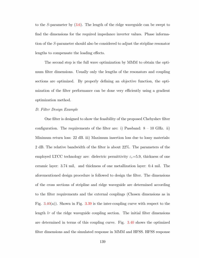
to the S-parameter by (3.6). The length of the ridge waveguide can be swept to
�nd the dimensions for the required impedance inverter values. Phase informa-
tion of the S-parameter should also be considered to adjust the stripline resonator
lengths to compensate the loading e¤ects.
The second step is the full wave optimization by MMM to obtain the opti-
mum �lter dimensions. Usually only the lengths of the resonators and coupling
sections are optimized. By properly de�ning an objective function, the opti-
mization of the �lter performance can be done very e¢ ciently using a gradient
optimization method.
D. Filter Design Example
One �lter is designed to show the feasibility of the proposed Chebyshev �lter
con�guration. The requirements of the �lter are: i) Passband: 8 �10 GHz. ii)
Minimum return loss: 22 dB. iii) Maximum insertion loss due to lossy materials:
2 dB. The relative bandwidth of the �lter is about 22%. The parameters of the
employed LTCC technology are: dielectric permittivity "r=5.9, thickness of one
ceramic layer: 3.74 mil, and thickness of one metallization layer: 0.4 mil. The
aforementioned design procedure is followed to design the �lter. The dimensions
of the cross sections of stripline and ridge waveguide are determined according
to the �lter requirements and the external couplings (Chosen dimensions as in
Fig. 3.40(a)). Shown in Fig. 3.39 is the inter-coupling curve with respect to the
length lr of the ridge waveguide coupling section. The initial �lter dimensions
are determined in terms of this coupling curve. Fig. 3.40 shows the optimized
�lter dimensions and the simulated response in MMM and HFSS. HFSS response
139
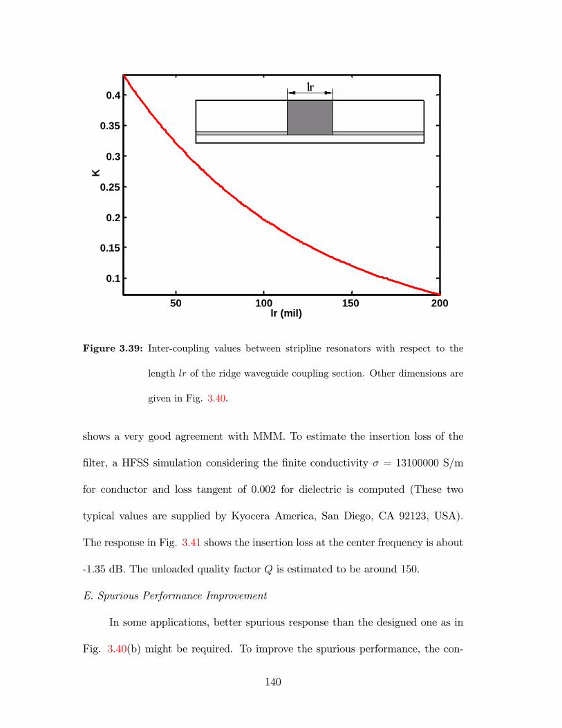
50 100 150 200
0.1
0.15
0.2
0.25
0.3
0.35
0.4
lr (mil)
K
50 100 150 200
0.1
0.15
0.2
0.25
0.3
0.35
0.4
lr (mil)
K
Figure 3.39: Inter-coupling values between stripline resonators with respect to the
length lr of the ridge waveguide coupling section. Other dimensions are
given in Fig. 3.40.
shows a very good agreement with MMM. To estimate the insertion loss of the
�lter, a HFSS simulation considering the �nite conductivity � = 13100000 S/m
for conductor and loss tangent of 0.002 for dielectric is computed (These two
typical values are supplied by Kyocera America, San Diego, CA 92123, USA).
The response in Fig. 3.41 shows the insertion loss at the center frequency is about
-1.35 dB. The unloaded quality factor Q is estimated to be around 150.
E. Spurious Performance Improvement
In some applications, better spurious response than the designed one as in
Fig. 3.40(b) might be required. To improve the spurious performance, the con-
140
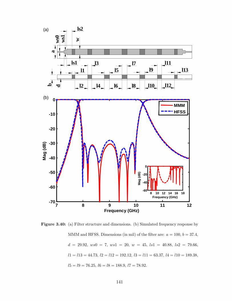
aws
0ws
1
w
b d
l1
l2
l3 l7
l4
l5
l6 l8
l9
l10
l11
l12
l13ls1
ls2
7 8 9 10 11 1270
60
50
40
30
20
10
0
Mag
(dB
)
Frequency (GHz)
MMMHFSS
7 8 9 10 11 1270
60
50
40
30
20
10
0
Mag
(dB
)
Frequency (GHz)
MMMHFSS
8 10 12 14 16 1860
40
20
0
Mag
(dB
)
Frequency (GHz)8 10 12 14 16 18
60
40
20
0
Mag
(dB
)
Frequency (GHz)
(a)
(b)
Figure 3.40: (a) Filter structure and dimensions. (b) Simulated frequency response by
MMM and HFSS. Dimensions (in mil) of the �lter are: a = 100, b = 37:4,
d = 29:92, ws0 = 7, ws1 = 20, w = 45, ls1 = 40:88, ls2 = 79:66,
l1 = l13 = 44:73, l2 = l12 = 192:12, l3 = l11 = 63:37, l4 = l10 = 189:38,
l5 = l9 = 76:25, l6 = l8 = 188:9, l7 = 78:92.
141
7 7.5 8 8.5 9 9.5 10 10.5 11 11.560
50
40
30
20
10
0
Mag
nitu
de (d
B)
Frequency (GHz)
HFSS: S11
HFSS: S21
7 7.5 8 8.5 9 9.5 10 10.5 11 11.560
50
40
30
20
10
0
Mag
nitu
de (d
B)
Frequency (GHz)
HFSS: S11
HFSS: S21
7.5 8 8.5 9 9.5 10 10.52
1.8
1.6
1.4
1.2
7.5 8 8.5 9 9.5 10 10.52
1.8
1.6
1.4
1.2
Figure 3.41: Frequency response with lossy material (conductivity � = 13100000 S/m
and loss tangent is 0.002).
cept of stepped impedance resonators (SIRs) can be applied [155�158]. Basically,
a wider-strip lower-impedance stripline is introduced in the middle of the orig-
inal stripline resonator (as in Fig 3.42(a)). This wider stripline will reduce the
total length of the resonator to have a fundamental resonant mode at the center
frequency f0 because the �eld of this mode is concentrated around the middle of
the resonator and this wider stripline introduces very strong coupling e¤ect for
it. While for the �rst higher order resonant mode, the �eld is very weak in the
middle of the resonator and very strong close to the two ends. Therefore, the
wider stripline will push the �rst higher order mode further away from f0 since
142
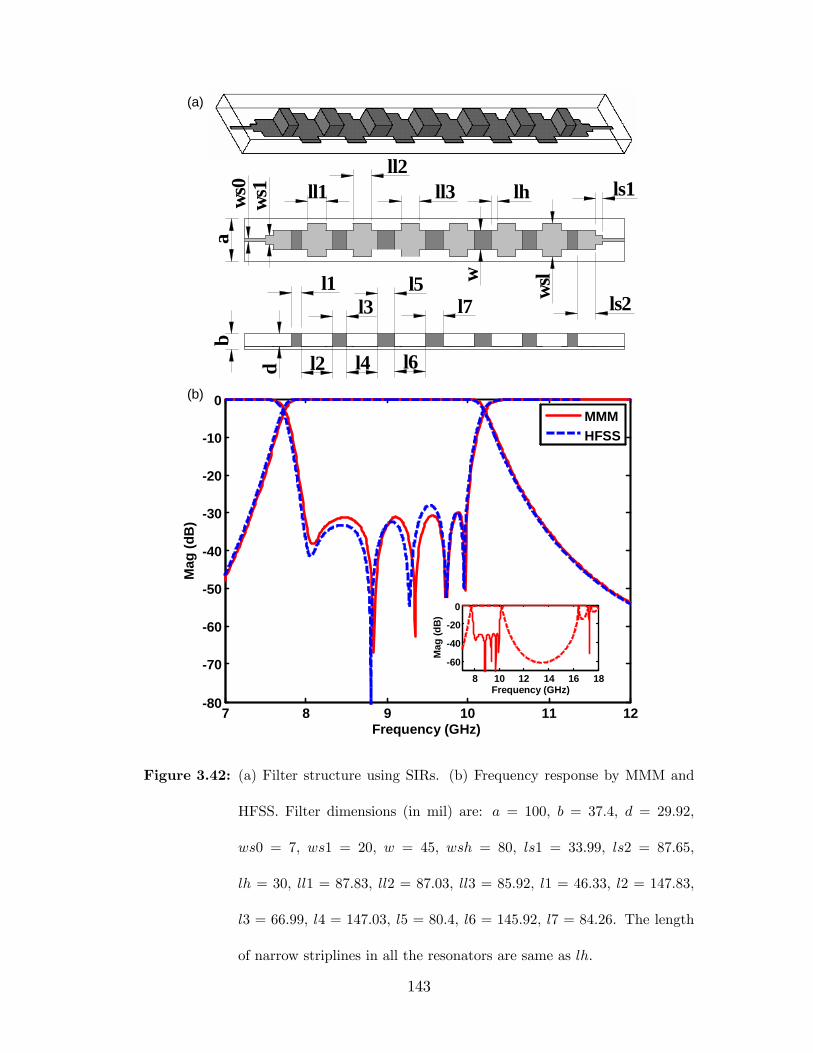
ab
dws
1ws
0
l1l3
l2 l4
l5
l6
l7
ll1ll2
ll3 lh
wsl
ls2
ls1
w
7 8 9 10 11 1280
70
60
50
40
30
20
10
0
Mag
(dB
)
Frequency (GHz)
MMMHFSS
7 8 9 10 11 1280
70
60
50
40
30
20
10
0
Mag
(dB
)
Frequency (GHz)
MMMHFSS
8 10 12 14 16 1860
40
20
0
Mag
(dB
)
Frequency (GHz)8 10 12 14 16 18
60
40
20
0
Mag
(dB
)
Frequency (GHz)
(a)
(b)
Figure 3.42: (a) Filter structure using SIRs. (b) Frequency response by MMM and
HFSS. Filter dimensions (in mil) are: a = 100, b = 37:4, d = 29:92,
ws0 = 7, ws1 = 20, w = 45, wsh = 80, ls1 = 33:99, ls2 = 87:65,
lh = 30, ll1 = 87:83, ll2 = 87:03, ll3 = 85:92, l1 = 46:33; l2 = 147:83,
l3 = 66:99, l4 = 147:03, l5 = 80:4, l6 = 145:92, l7 = 84:26. The length
of narrow striplines in all the resonators are same as lh.
143
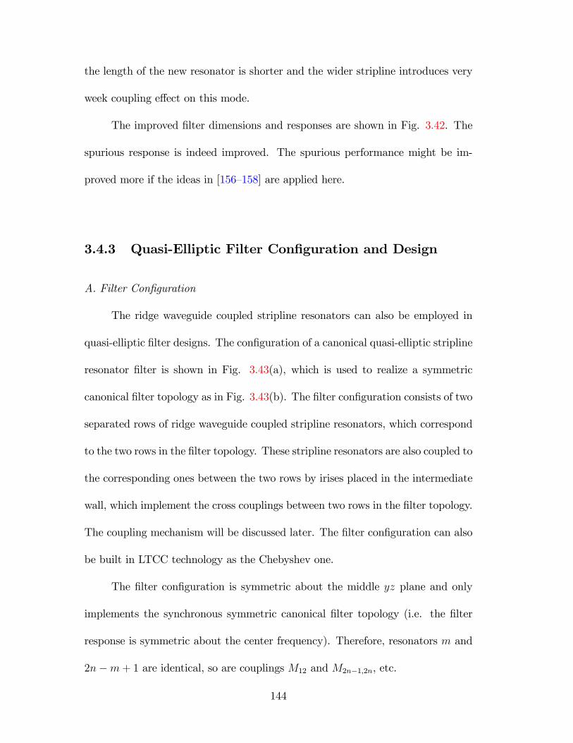
the length of the new resonator is shorter and the wider stripline introduces very
week coupling e¤ect on this mode.
The improved �lter dimensions and responses are shown in Fig. 3.42. The
spurious response is indeed improved. The spurious performance might be im-
proved more if the ideas in [156�158] are applied here.
3.4.3 Quasi-Elliptic Filter Con�guration and Design
A. Filter Con�guration
The ridge waveguide coupled stripline resonators can also be employed in
quasi-elliptic �lter designs. The con�guration of a canonical quasi-elliptic stripline
resonator �lter is shown in Fig. 3.43(a), which is used to realize a symmetric
canonical �lter topology as in Fig. 3.43(b). The �lter con�guration consists of two
separated rows of ridge waveguide coupled stripline resonators, which correspond
to the two rows in the �lter topology. These stripline resonators are also coupled to
the corresponding ones between the two rows by irises placed in the intermediate
wall, which implement the cross couplings between two rows in the �lter topology.
The coupling mechanism will be discussed later. The �lter con�guration can also
be built in LTCC technology as the Chebyshev one.
The �lter con�guration is symmetric about the middle yz plane and only
implements the synchronous symmetric canonical �lter topology (i.e. the �lter
response is symmetric about the center frequency). Therefore, resonators m and
2n�m+ 1 are identical, so are couplings M12 and M2n�1;2n, etc.
144
plane xz
plane yz
1 2 n
2n 2n1 n+1
1 2
Rout
Rin
n
M1,2n
M2n1,2n
M2,2n1
2n 2n1 n+1
Mn,n+1
M1,2
(a)
(b)
Figure 3.43: (a) Physical con�guration of canonical �lter topology using stripline res-
onators. (b) Canonical topology of 2n resonator symmetric quasi-elliptic
�lter.
145
B. Coupling Mechanism
The canonical �lter topology as in Fig. 3.43(b) has adjacent couplings
Mi;i+1 along the two rows and cross couplings Mi;2n�i+1 between the two rows
(in some cases, some of Mi;2n�i+1 might be zero). The adjacent couplings Mi;i+1
are achieved by the ridge waveguide evanescent mode coupling sections between
the stripline resonators, similar as the previously presented Chebyshev case. These
adjacent couplings are mainly magnetic couplings and have positive signs. Cross
couplingsMi;2n�i+1 include two types of couplings: electric coupling and magnetic
coupling, which correspond to negative and positive sign couplings, respectively.
The realization of electric cross coupling is shown in Fig. 3.44(a). A small
iris window is opened inside the separation wall at the center position of the
stripline resonators. The broad sides of these two striplines are placed close to
each other through this iris window. The electric coupling is provided by the
interaction of the fringing �elds of these two striplines. The coupling strength can
be controlled by the coupled length of the two striplines and the separation space
between them.
The realization of magnetic cross coupling is shown in Fig. 3.44(b). Ridge
waveguides are sandwiched inside two stripline resonators �rst, and then coupled
to each other through the iris window opened inside the separation wall. The ridge
waveguide is to transform the TEM mode of stripline to TE/TM modes. The iris
coupling is then mainly provided by the magnetic �elds of the fundamental TE
modes of the ridge waveguides. The coupling strength can be controlled by the size
of the ridge waveguide and the separation between them. If very strong coupling
146
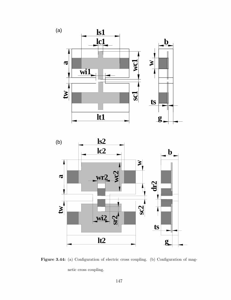
a
ls1lc1
sc1tw
wc1
b
w
g
ts
lt1
wi1a
lt2
tw
ls2lc2
wc2
wr2
sc2
wi2
bdr
2
g
ts
w
sr2
(a)
(b)
Figure 3.44: (a) Con�guration of electric cross coupling. (b) Con�guration of mag-
netic cross coupling.
147
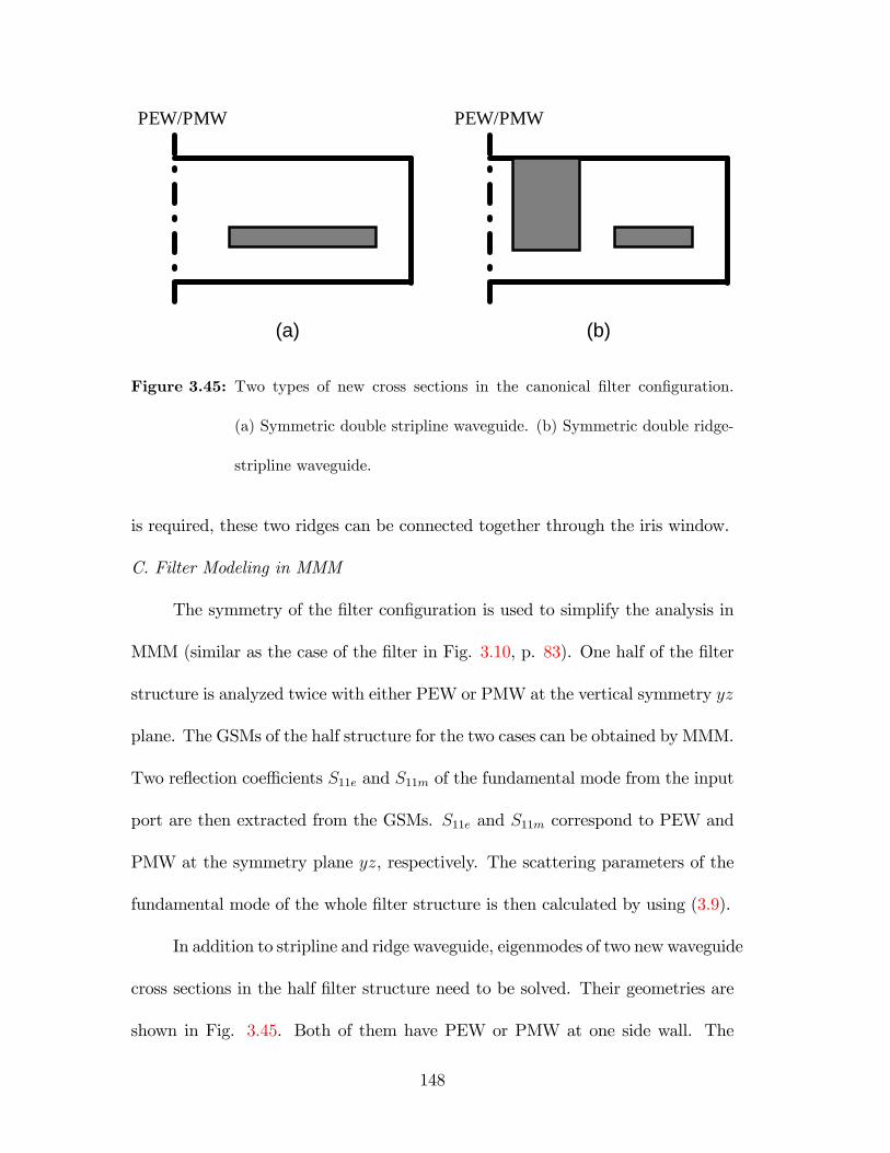
PEW/PMW PEW/PMW
(a) (b)
Figure 3.45: Two types of new cross sections in the canonical �lter con�guration.
(a) Symmetric double stripline waveguide. (b) Symmetric double ridge-
stripline waveguide.
is required, these two ridges can be connected together through the iris window.
C. Filter Modeling in MMM
The symmetry of the �lter con�guration is used to simplify the analysis in
MMM (similar as the case of the �lter in Fig. 3.10, p. 83). One half of the �lter
structure is analyzed twice with either PEW or PMW at the vertical symmetry yz
plane. The GSMs of the half structure for the two cases can be obtained by MMM.
Two re�ection coe¢ cients S11e and S11m of the fundamental mode from the input
port are then extracted from the GSMs. S11e and S11m correspond to PEW and
PMW at the symmetry plane yz, respectively. The scattering parameters of the
fundamental mode of the whole �lter structure is then calculated by using (3.9).
In addition to stripline and ridge waveguide, eigenmodes of two new waveguide
cross sections in the half �lter structure need to be solved. Their geometries are
shown in Fig. 3.45. Both of them have PEW or PMW at one side wall. The
148
analysis method of these two cross sections is based on the GTR technique (see
Appendix A, p. 255). Two kinds of TEM modes exist in these two cross sections:
even TEM mode corresponding to PMW and odd TEM mode corresponding to
PEW. The typical electric �eld distributions of the two TEM modes inside the
cross section of Fig. 3.45(a) are shown in Fig. B.2(a) and (b) (p. 270). For the
cross section in Fig. 3.45(b), the electric �eld distributions of two TEM modes
and two TE modes are shown in Fig. B.2(c)�(e). The GSMs of each discontinuity
can be calculated by using the formulations in Appendix C (p. 271).
D. Filter Design Procedure
The design procedure consists of two steps, similar to the Chebyshev case.
In the �rst step, the initial dimensions of the �lter are obtained according to the
required coupling values. Basically each coupling value is matched with some
physical dimensions. For external coupling R and adjacent couplings Mi;i+1, the
impedance inverter method is used. The relationships between inverter K and
normalized couplings Mi;i+1 and R are [3, 159]
K01 = K2n;2n+1 =
s�
2
bw
f0R �
sf 20
f 20 � f 2c
Ki;i+1 =�
2
bw
f0Mi;i+1 �
f 20f 20 � f 2c
(3.21)
where f0 and bw are center frequency and bandwidth of the �lter. fc is the cuto¤
frequency of the fundamental mode of the waveguide. In this presented case, fc
is zero. For cross couplings Mi;2n�i+1, the two resonant frequencies fe and fm
(corresponding to a PEW and a PMW between two resonators, respectively) are
computed for the structures in Fig. 3.44. Coupling value M in frequency unit
149
and loaded resonant frequency fl are obtained as (extended from (3.5))
M =f 2e � f 2mf 2e + f 2m
� fl and fl =pfefm (3.22)
In the second step, the �lter is analyzed and optimized using MMM to
improve the performance and obtain an optimum design.
E. Filter Design Example
To demonstrate the feasibility of the proposed quasi-elliptic �lter con�g-
uration, a design of four-pole-two-zero �lter with a center frequency of 9 GHz
and bandwidth 900 MHz is performed. The minimum return loss is 22 dB. The
equivalent circuit satisfying the speci�cations can be synthesized using the method
presented in chapter 2. The synthesized prototype circuit has normalized external
coupling R = 1:15444 and a coupling matrix
M =
266666666664
0 M12 0 M14
M12 0 M23 0
0 M23 0 M34
M14 0 M34 0
377777777775(3.23)
with adjacent couplings M12 = M34 = 0:9370 and cross couplings M23 = 0:7650
and M14 = �0:1026.
The cross sections of the stripline resonators and ridge waveguides are chosen
identical as the previous Chebyshev �lter example since the center frequencies are
identical. The length of the ridge waveguide coupling section is swept to �nd
the dimension for the adjacent couplings M12 and M34. The coupling curve is
shown in Fig. 3.39. The coupling curves to determine the dimensions for cross
150
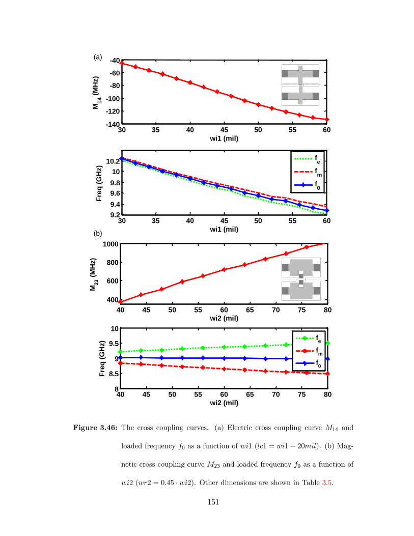
40 45 50 55 60 65 70 75 808
8.5
9
9.5
10
wi2 (mil)
Freq
(GH
z)
40 45 50 55 60 65 70 75 80400
600
800
1000
wi2 (mil)
M23
(MH
z)
fefmf0
40 45 50 55 60 65 70 75 808
8.5
9
9.5
10
wi2 (mil)
Freq
(GH
z)
40 45 50 55 60 65 70 75 808
8.5
9
9.5
10
wi2 (mil)
Freq
(GH
z)
40 45 50 55 60 65 70 75 80400
600
800
1000
wi2 (mil)
M23
(MH
z)
fefmf0
30 35 40 45 50 55 60140
120
100
80
60
40
wi1 (mil)
M14
(MH
z)
30 35 40 45 50 55 609.29.49.69.810
10.2
wi1 (mil)
Freq
(GH
z)
fefmf0
30 35 40 45 50 55 60140
120
100
80
60
40
wi1 (mil)
M14
(MH
z)
30 35 40 45 50 55 609.29.49.69.810
10.2
30 35 40 45 50 55 60140
120
100
80
60
40
wi1 (mil)
M14
(MH
z)
30 35 40 45 50 55 609.29.49.69.810
10.2
wi1 (mil)
Freq
(GH
z)
fefmf0
(a)
(b)
Figure 3.46: The cross coupling curves. (a) Electric cross coupling curve M14 and
loaded frequency f0 as a function of wi1 (lc1 = wi1� 20mil). (b) Mag-
netic cross coupling curve M23 and loaded frequency f0 as a function of
wi2 (wr2 = 0:45 � wi2). Other dimensions are shown in Table 3.5.
151
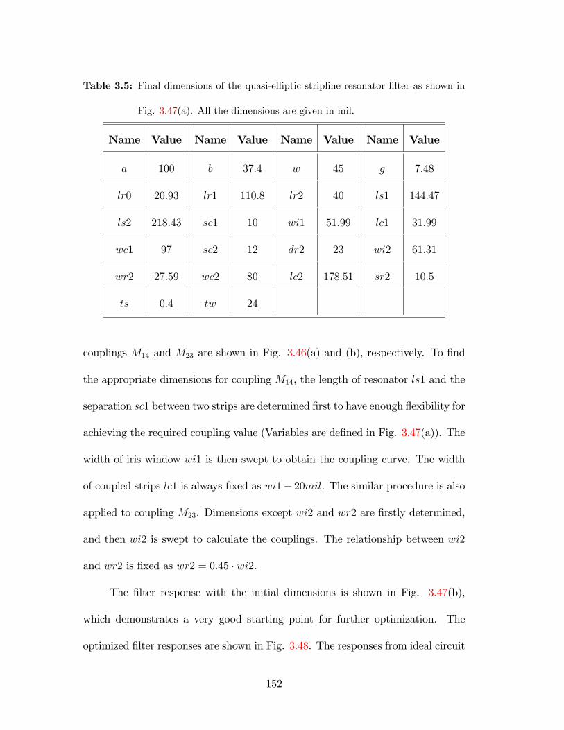
Table 3.5: Final dimensions of the quasi-elliptic stripline resonator �lter as shown in
Fig. 3.47(a). All the dimensions are given in mil.
Name Value Name Value Name Value Name Value
a 100 b 37:4 w 45 g 7:48
lr0 20:93 lr1 110:8 lr2 40 ls1 144:47
ls2 218:43 sc1 10 wi1 51:99 lc1 31:99
wc1 97 sc2 12 dr2 23 wi2 61:31
wr2 27:59 wc2 80 lc2 178:51 sr2 10:5
ts 0:4 tw 24
couplings M14 and M23 are shown in Fig. 3.46(a) and (b), respectively. To �nd
the appropriate dimensions for coupling M14, the length of resonator ls1 and the
separation sc1 between two strips are determined �rst to have enough �exibility for
achieving the required coupling value (Variables are de�ned in Fig. 3.47(a)). The
width of iris window wi1 is then swept to obtain the coupling curve. The width
of coupled strips lc1 is always �xed as wi1� 20mil. The similar procedure is also
applied to coupling M23. Dimensions except wi2 and wr2 are �rstly determined,
and then wi2 is swept to calculate the couplings. The relationship between wi2
and wr2 is �xed as wr2 = 0:45 � wi2.
The �lter response with the initial dimensions is shown in Fig. 3.47(b),
which demonstrates a very good starting point for further optimization. The
optimized �lter responses are shown in Fig. 3.48. The responses from ideal circuit
152
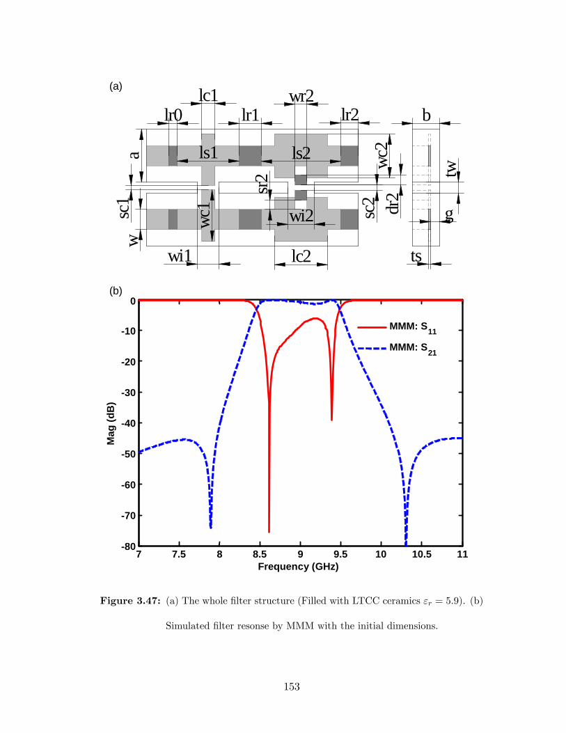
a ls1 ls2
lr1 lr2sc
1
lc2
wi2
wr2
dr2
sc2
lr0lc1
wi1
wc1
wc2
sr2
bw
ts
tw
g
7 7.5 8 8.5 9 9.5 10 10.5 1180
70
60
50
40
30
20
10
0
Mag
(dB
)
Frequency (GHz)
MMM: S11
MMM: S21
7 7.5 8 8.5 9 9.5 10 10.5 1180
70
60
50
40
30
20
10
0
Mag
(dB
)
Frequency (GHz)
MMM: S11
MMM: S21
(a)
(b)
Figure 3.47: (a) The whole �lter structure (Filled with LTCC ceramics "r = 5:9). (b)
Simulated �lter resonse by MMM with the initial dimensions.
153
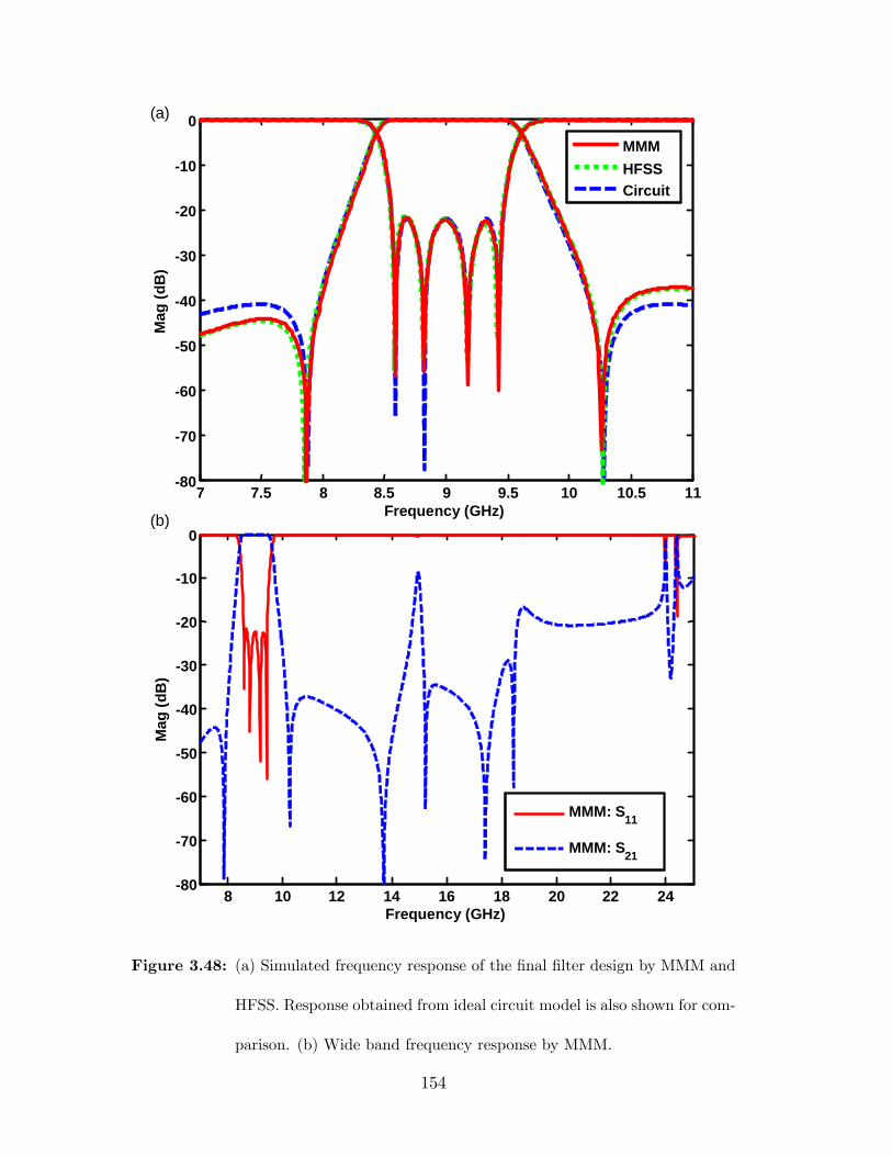
8 10 12 14 16 18 20 22 2480
70
60
50
40
30
20
10
0
Mag
(dB
)
Frequency (GHz)
MMM: S11
MMM: S21
8 10 12 14 16 18 20 22 2480
70
60
50
40
30
20
10
0
Mag
(dB
)
Frequency (GHz)
MMM: S11
MMM: S21
7 7.5 8 8.5 9 9.5 10 10.5 1180
70
60
50
40
30
20
10
0
Frequency (GHz)
Mag
(dB
)MMMHFSSCircuit
7 7.5 8 8.5 9 9.5 10 10.5 1180
70
60
50
40
30
20
10
0
Frequency (GHz)
Mag
(dB
)MMMHFSSCircuit
(a)
(b)
Figure 3.48: (a) Simulated frequency response of the �nal �lter design by MMM and
HFSS. Response obtained from ideal circuit model is also shown for com-
parison. (b) Wide band frequency response by MMM.
154
mode, MMM and HFSS are all shown in Fig. 3.48(a) for comparison. HFSS result
shows a very good agreement with MMM. The wide band frequency response is
shown in Fig. 3.48(b). The S21 spurious response around the second harmonic is
suppressed below -10 dB by the stepped impedance resonators in the �lter. The
�nal �lter dimensions are shown in Table 3.5.
3.5 Dual-mode Asymmetric Filters in Circular
Waveguides
3.5.1 Introduction
High performance waveguide �lters with high Q cavities may take up a signi�cant
physical volume, which is disadvantageous in many telecommunications and space
applications. One method of size reduction is to exploit the existence of multiple
degenerate modes in waveguide cavities. For example, one dual-mode cavity can
be employed to implement two resonant circuits in one �lter (Assuming the cou-
pling between the two modes can be realized mechanically), such that the number
of cavities required to realize an N -degree �lter is reduced to N=2 (N is even) and,
therefore, the physical �lter volume is more compact than the �lter realized by
single-mode cavities (N single-mode cavities are required for an N -degree �lter).
Multiple-mode cavity �lter were �rst reported by Lin in 1951 [160]. The concept
was then extended to dual-, triple-, and quadruple-mode coupled cavity �lters
[161�164]. Since then, multiple-mode coupled cavity/resonator �lters have been
155
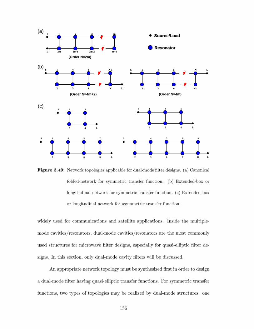
S 1 2 3 m
m+12m22m12mL
S 1 2 3 m
m+12m22m12mL
(a)
S 1
2 3
4 5
6 N
N1
L
S 1
2 3
4 5
6 N
N1
L
(b)
Source/Load
Resonator
Source/Load
Resonator
(Order N=2m)
(Order N=4m+2) (Order N=4m)
S 1
2 3
4 5
6 N1
N LS 1
2 3
4 5
6 N1
N L
S 1
2 4
3
L
S 1
2 3
4 5
6 L
S 1
2 3
4 5
6 8
7
L
S 1
2 3
4 5
6 7
8
L10
9
(c)
Figure 3.49: Network topologies applicable for dual-mode �lter designs. (a) Canonical
folded-network for symmetric transfer function. (b) Extended-box or
longitudinal network for symmetric transfer function. (c) Extended-box
or longitudinal network for asymmetric transfer function.
widely used for communications and satellite applications. Inside the multiple-
mode cavities/resonators, dual-mode cavities/resonators are the most commonly
used structures for microwave �lter designs, especially for quasi-elliptic �lter de-
signs. In this section, only dual-mode cavity �lters will be discussed.
An appropriate network topology must be synthesized �rst in order to design
a dual-mode �lter having quasi-elliptic transfer functions. For symmetric transfer
functions, two types of topologies may be realized by dual-mode structures. one
156
type is the canonical folded-network topology as shown in Fig. 3.49(a). Any two
resonators in one column (e.g. 1 and 2m, m and m+1, etc.) can be implemented
by one dual-mode cavity/resonator. The two rows/lines in this network topology
are symmetric, which will simplify the hardware implementations of the couplings
between two dual-mode cavities. However, one drawback of this topology is that
the source and load of the �lter will be in the same physical dual-mode cavity,
which sometimes might not be practical. The other type is the extended-box or
longitudinal topology as shown in Fig. 3.49(b), in which the source and load are at
opposite ends. Even though this network topology is not symmetric, the produced
frequency response is still symmetric about the center frequency. When the �lter
order N = 4m + 2, the source and load are in the same line/row, which means
that they are exciting the same polarized mode of the dual-mode cavities. When
the �lter order N = 4m, the source and load are in di¤erent lines, which means
that they are exciting two di¤erent polarized modes of the dual-mode cavities.
The number of �nite transmission zeros produced by this longitudinal topology is
constrained by the number of resonators along the minimum path between source
and load because each resonator along this minimum path corresponds to a trans-
mission zero at in�nity. Therefore, the maximum number of �nite transmission
zeros that can be generated by a longitudinal topology is given by [57]
Nz;max =
8>><>>:N2� 1 = 2m for N = 4m+ 2
N2= 2m for N = 4m
(3.24)
The analytical synthesis procedure of the longitudinal topology for symmetric
transfer functions is given in [88] for N = 6; 8; 10; 12; and 14. For higher order
157
�lters, optimization procedure can be employed.
For asymmetric transfer function, the longitudinal topologies for 4th, 6th,
8th, and 10th order �lters as shown in Fig. 3.49(c) are appropriate for dual-mode
realizations. The source and load are always in di¤erent lines. The maximum
number of �nite transmission zeros that can be produced by this type of topology
is (m � 1) for a �lter order of N = 2m, which can be seen through the afore-
explained minimum path rule. The synthesis procedure of this kind of topology
based on optimization method is given in [83].
Various dual-mode implementations of symmetric quasi-elliptic �lters can be
found in literature. In this section, in order to demonstrate the feasibility of dual-
mode realization of asymmetric quasi-elliptic �lters, a 4-pole �lter with one trans-
mission zero is synthesized and implemented by dual-mode circular waveguide
cavities. The detailed design procedure and measurement results are given next.
Similar structure and design procedure can also be applied for higher order dual-
mode asymmetric �lter designs.
3.5.2 Filter Parameters
A 4-pole-1-zero quasi-elliptic �lter with bandwidth 35 MHz about the center fre-
quency 3.38 GHz is designed. The minimum return loss within the pass band is
required to be 22 dB. The maximum insertion loss within the passband is 0.3 dB.
Two di¤erent solutions are possible according to the location of the transmission
zero (one is within the lower stopband and the other one is within the upper stop-
158
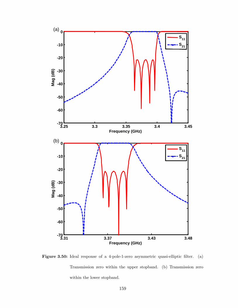
3.25 3.3 3.35 3.4 3.4570
60
50
40
30
20
10
0
Frequency (GHz)
Mag
(dB
)
S11
S21
3.25 3.3 3.35 3.4 3.4570
60
50
40
30
20
10
0
Frequency (GHz)
Mag
(dB
)
S11
S21
3.31 3.37 3.43 3.4870
60
50
40
30
20
10
0
Frequency (GHz)
Mag
(dB
)
S11
S21
3.31 3.37 3.43 3.4870
60
50
40
30
20
10
0
Frequency (GHz)
Mag
(dB
)
S11
S21
(a)
(b)
Figure 3.50: Ideal response of a 4-pole-1-zero asymmetric quasi-elliptic �lter. (a)
Transmission zero within the upper stopband. (b) Transmission zero
within the lower stopband.
159
band.). The coupling matrices of the 4th-order longitudinal topology as in Fig.
3.49(c) for these two solutions are given as
MU =
266666666664
0:0402 0:7673 �0:5590 0
0:7673 0:5662 0 0:7673
�0:5590 0 �0:8582 0:5590
0 0:7673 0:5590 0:0402
377777777775
ML =
266666666664
�0:0402 0:7673 �0:5590 0
0:7673 �0:5662 0 0:7673
�0:5590 0 0:8582 0:5590
0 0:7673 0:5590 �0:0402
377777777775Rin = Rout = 1:1496 (3.25)
whereMU is the solution for the �lter with a zero within the upper stopband and
ML is for the �lter with a zero within the lower stopband. The ideal frequency
responses for these two cases are shown in Fig. 3.50(a) and (b), respectively.
The location of transmission zero is only determined by the frequency o¤sets of
the resonators, in other words, the signs of the self-coupling term Mii in the
coupling matrix. When the signs of all Mii are changed to the opposite ones, the
transmission zero will move to the opposite side of the stopband. The relationship
betweenMii and the frequency o¤sets of resonators for narrow bandwidth �lter is
approximately given by
fi � f0 �1
2Mii �BW (3.26)
160
where fi is the shifted resonant frequency of each resonator. f0 is the center
frequency of the �lter. Mii is the normalized self-coupling coe¢ cient. BW is the
bandwidth of the �lter. In practice, asymmetric quasi-elliptic �lters are mostly
used in the front end of the transmitter/receiver diplexers in base stations. The
transmission zeros are, therefore, placed between the adjacent channels to obtain
the high rejection to prevent the interference.
3.5.3 Physical Implementation
Dual-mode circular waveguide cavities operating with dual TE111 resonant modes
are used to realize the synthesized ideal longitudinal network. The diagram of the
implementation structure is shown in Fig. 3.51(a). The manufactured parts are
shown in Fig. 3.51(b) and the assembled �lter hardware is shown in Fig. 3.51(c).
The external input and output couplings (Rin andRout) are provided by the probes
of SMA connectors. The two SMA connectors are positioned perpendicular to
each other to excite the two polarizations of the TE111 resonant mode. Resonant
frequencies (fi) and cross couplings (Mij, i 6= j) are adjusted by tuning screws,
coupling screws and coupling iris as shown in Fig. 3.51(a) and (b). The tuning
screws must be aligned with either of the SMA probes to modify the resonant
frequency fi, while the coupling screws must be placed at the position of 45
degrees from the tuning screws and the SMA probes to introduce the cross coupling
between two orthogonal polarizations. In order to produce two cross couplings
with di¤erent signs, the two coupling screws inside two consecutive cavities must
161
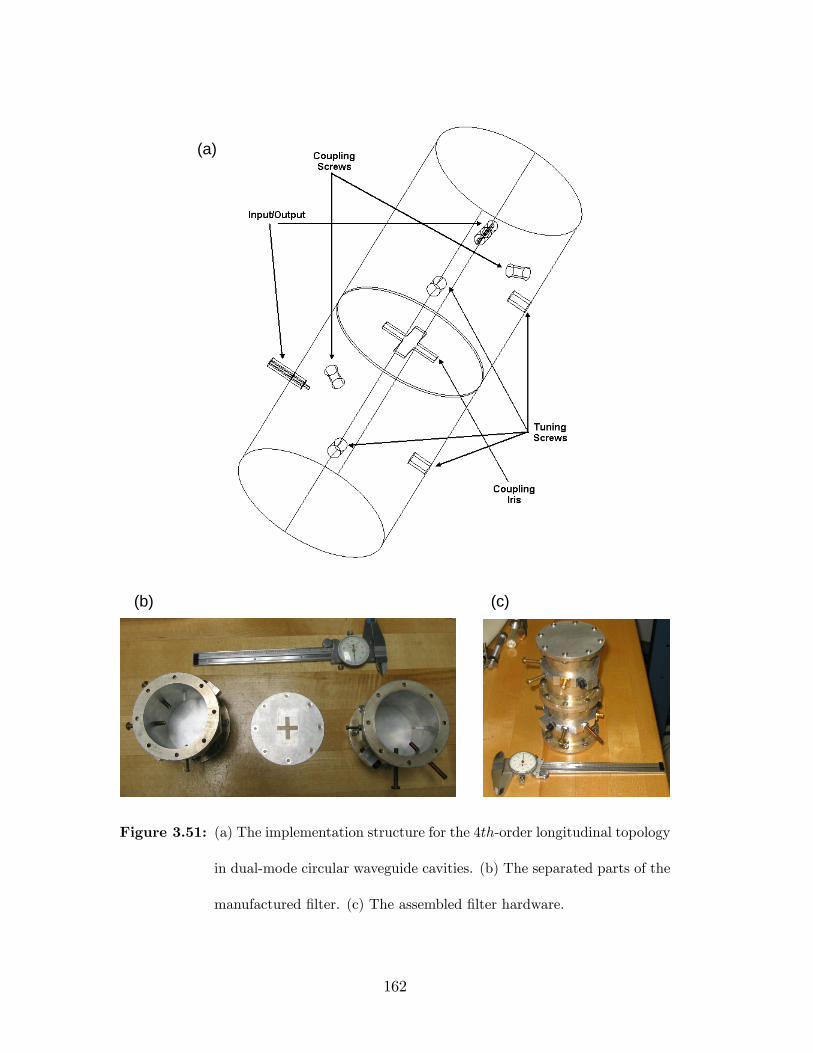
(a)
(b) (c)
Figure 3.51: (a) The implementation structure for the 4th-order longitudinal topology
in dual-mode circular waveguide cavities. (b) The separated parts of the
manufactured �lter. (c) The assembled �lter hardware.
162
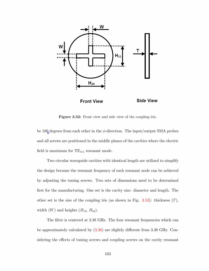
Figure 3.52: Front view and side view of the coupling iris.
be 180 degrees from each other in the �-direction. The input/output SMA probes
and all screws are positioned in the middle planes of the cavities where the electric
�eld is maximum for TE111 resonant mode.
Two circular waveguide cavities with identical length are utilized to simplify
the design because the resonant frequency of each resonant node can be achieved
by adjusting the tuning screws. Two sets of dimensions need to be determined
�rst for the manufacturing. One set is the cavity size: diameter and length. The
other set is the size of the coupling iris (as shown in Fig. 3.52): thickness (T ),
width (W ) and heights (H13, H24).
The �lter is centered at 3.38 GHz. The four resonant frequencies which can
be approximately calculated by (3.26) are slightly di¤erent from 3.38 GHz. Con-
sidering the e¤ects of tuning screws and coupling screws on the cavity resonant
163

frequency, the cavity size should be chosen to have a higher TE111 resonant fre-
quency than 3.38 GHz. The cavity size is �nally selected to have a diameter of
2.4 inch and a length of 3.08 inch, which has a TE111 resonant frequency at about
3.46 GHz.
The dimensions of the coupling iris can be approximately decided by model-
ing the slot coupling structure between two identical cavities without considering
the e¤ects from the screws. Either MMM or FEM in HFSS is suitable for analyz-
ing such structure. The iris thickness T and the identical widthW of the two slots
are chosen to be �xed (T = 0:032", W = 0:1875"). The height of each slot is then
swept to search for H13 and H24 to have the coupling values of M13 and M24 (As-
suming resonant node 1 and 2 are realized by one physical cavity, and node 3 and
4 are realized by the other cavity), respectively. The calculation method for the
coupling values between two identical cavities is following the same way as before,
i.e. using the two resonant frequency points fe and fm corresponding to PEW
and PMW at the symmetric plane, respectively. The determined dimensions for
H13 and H24 are 0:905" and 1:0", respectively.
3.5.4 Measurement Results
The manufactured �lter hardware is shown in Fig. 3.51(b) and (c). A systematic
tuning procedure is employed to �nd the optimum positions of all the screws.
Each dual-mode cavity is tuned separately based on the phase response of S11
of the one-port network. The external input/output couplings and the resonant
164
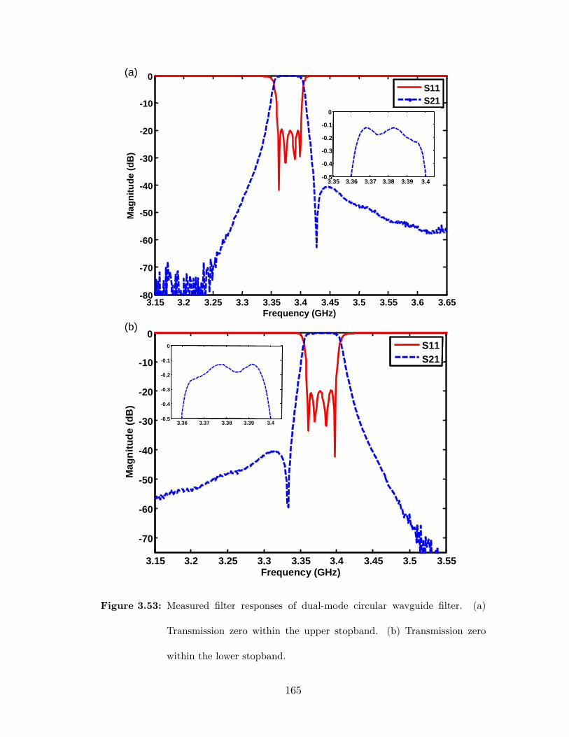
3.15 3.2 3.25 3.3 3.35 3.4 3.45 3.5 3.55
70
60
50
40
30
20
10
0
Frequency (GHz)
Mag
nitu
de (d
B)
S11S21
3.15 3.2 3.25 3.3 3.35 3.4 3.45 3.5 3.55
70
60
50
40
30
20
10
0
Frequency (GHz)
Mag
nitu
de (d
B)
S11S21
3.15 3.2 3.25 3.3 3.35 3.4 3.45 3.5 3.55 3.6 3.6580
70
60
50
40
30
20
10
0
Frequency (GHz)
Mag
nitu
de (d
B)
S11S21
3.15 3.2 3.25 3.3 3.35 3.4 3.45 3.5 3.55 3.6 3.6580
70
60
50
40
30
20
10
0
Frequency (GHz)
Mag
nitu
de (d
B)
S11S21
3.35 3.36 3.37 3.38 3.39 3.40.5
0.4
0.3
0.2
0.1
0
3.35 3.36 3.37 3.38 3.39 3.40.5
0.4
0.3
0.2
0.1
0
3.36 3.37 3.38 3.39 3.40.5
0.4
0.3
0.2
0.1
0
3.36 3.37 3.38 3.39 3.40.5
0.4
0.3
0.2
0.1
0
(a)
(b)
Figure 3.53: Measured �lter responses of dual-mode circular wavguide �lter. (a)
Transmission zero within the upper stopband. (b) Transmission zero
within the lower stopband.
165
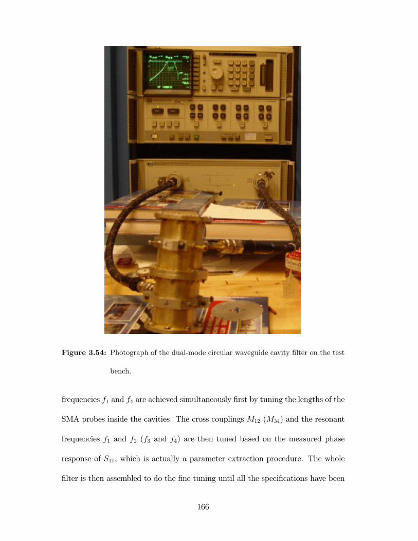
Figure 3.54: Photograph of the dual-mode circular waveguide cavity �lter on the test
bench.
frequencies f1 and f4 are achieved simultaneously �rst by tuning the lengths of the
SMA probes inside the cavities. The cross couplings M12 (M34) and the resonant
frequencies f1 and f2 (f3 and f4) are then tuned based on the measured phase
response of S11, which is actually a parameter extraction procedure. The whole
�lter is then assembled to do the �ne tuning until all the speci�cations have been
166
satis�ed. The measured �nal �lter responses are shown in Fig. 3.53(a) and (b) for
the two di¤erent solutions with di¤erent transmission zero locations, respectively.
The arrangement of the �lter measurement is shown in Fig. 3.54 for one solution.
For higher order asymmetric quasi-elliptic �lters, the tuning procedure will
be much more di¢ cult than the above presented one. The parameter extraction
method based on optimization and the aforementioned space mapping method
can then be employed to guide the tuning.
3.6 Dual-mode Quasi-Elliptic Filters in Rectan-
gular Waveguides
3.6.1 Introduction
Dual-mode quasi-elliptic function �lters are widely used in high-quality microwave
�lters and multiplexers due to their higher selectivity, smaller size and less mass
than single mode coupled resonator �lters [123, 161, 162, 165, 166]. The conven-
tional approaches, e.g. dual-mode circular waveguide �lter in previous section, to
couple dual modes is by adding a coupling screw at 45� angle from the direction
of the electric �elds of the two dual modes. By changing the penetration of the
coupling screw in the cavity, the coupling between the two dual modes can be
adjusted. Although the tuning and coupling screws provide �exibility for opti-
mizing the �lter response, the tuning process is time consuming and makes the
production of dual-mode �lters expensive. Another drawback is that the power
167
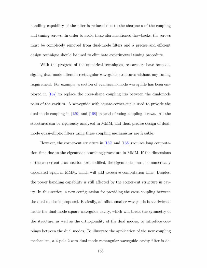
handling capability of the �lter is reduced due to the sharpness of the coupling
and tuning screws. In order to avoid these aforementioned drawbacks, the screws
must be completely removed from dual-mode �lters and a precise and e¢ cient
design technique should be used to eliminate experimental tuning procedure.
With the progress of the numerical techniques, researchers have been de-
signing dual-mode �lters in rectangular waveguide structures without any tuning
requirement. For example, a section of evanescent-mode waveguide has been em-
ployed in [167] to replace the cross-shape coupling iris between the dual-mode
pairs of the cavities. A waveguide with square-corner-cut is used to provide the
dual-mode coupling in [159] and [168] instead of using coupling screws. All the
structures can be rigorously analyzed in MMM, and thus, precise design of dual-
mode quasi-elliptic �lters using these coupling mechanisms are feasible.
However, the corner-cut structure in [159] and [168] requires long computa-
tion time due to the eigenmode searching procedure in MMM. If the dimensions
of the corner-cut cross section are modi�ed, the eigenmodes must be numerically
calculated again in MMM, which will add excessive computation time. Besides,
the power handling capability is still a¤ected by the corner-cut structure in cav-
ity. In this section, a new con�guration for providing the cross coupling between
the dual modes is proposed. Basically, an o¤set smaller waveguide is sandwiched
inside the dual-mode square waveguide cavity, which will break the symmetry of
the structure, as well as the orthogonality of the dual modes, to introduce cou-
plings between the dual modes. To illustrate the application of the new coupling
mechanism, a 4-pole-2-zero dual-mode rectangular waveguide cavity �lter is de-
168

signed in MMM. The same design procedure can also be used to design higher
order dual-mode �lters.
3.6.2 Filter Con�guration
Fig. 3.55(a) is the physical con�guration of the dual-mode rectangular waveguide
quasi-elliptic �lters which can be used to implement the topologies shown in Fig.
3.49(b) and (c). The structure can be manufactured either in air-�lled metallic
form or in LTCC technology.
The input and output ports are standard rectangular waveguides, while the
cavities are realized by square waveguides to support TE01 and TE10 degenerate
modes. The external coupling is provided by the evanescent-mode iris between
the port waveguide and the cavity. The port waveguide only supports a single
propagating mode (either TE10 or TE01, depending on the placement of the port
waveguide) in the interested frequency range, which will, therefore, only excite
one polarized mode in the cavity. The two port waveguides excite either the
same polarized mode (as shown in Fig. 3.55(a)) or the two di¤erent dual modes
depending on the �lter order and �lter topology as shown in Fig. 3.49(b) and (c).
In order to introduce the cross couplings between the dual modes in one
cavity, a smaller waveguide is added into the middle of the cavity as shown in Fig.
3.55(b). The center of this small waveguide is o¤set from the center of the square
waveguide for the cavity, thus, the double symmetry of the cavity is broken and a
coupling will be generated between the two originally orthogonal dual modes. For
169
(a)
(b)
Figure 3.55: (a) Physical con�guration of a rectangular waveguide quasi-elliptic func-
tion dual-mode �lter. (b) Cross coupling mechanism between the dual
modes.
170

symmetric quasi-elliptic function �lters, all the resonators are synchronized at the
center frequency, so this small waveguide will also be a square waveguide to have
the same e¤ect on the two polarizations. For asymmetric quasi-elliptic function
�lters, this small waveguide is usually not square to provide the di¤erent e¤ects
on the two polarizations because the resonators are not synchronized any more.
The coupling values between the dual modes in one cavity can be controlled by
adjusting the cross section and the length of the small waveguide, which dose not
add excessive mode-searching computation time and provides �exibility in dual-
mode coupling design. In quasi-elliptic �lter designs, couplings with di¤erent signs
are usually required. The small waveguides can be placed in opposite positions
with respect to the square cavity (as shown in Fig. 3.49(b)) to provide cross
couplings with di¤erent signs because the e¤ects on the �eld distribution will
introduce an equivalent 180� phase di¤erence. The resonant frequencies of the
dual resonant modes in one cavity are a¤ected by the coupling e¤ect of the small
waveguide and the lengths of the two separated square waveguides. Hence, it
is very �exible to control the self-couplings and the cross-coupling in one cavity,
which is especially important for asymmetric �lter designs.
Evanescent-mode waveguides (i.e. the rectangular irises between cavities
in Fig. 3.55(a)) are used to provide inter-couplings between dual-mode adjacent
cavities. This structure has advantages compared to the cross-shape iris: i) Mode-
searching procedure in MMM is avoided. ii) The numerical solution in MMM
converges much faster because fewer modes are required. iii) The coupling is
much less sensitive to the dimensional tolerances. The coupling values can be
171

controlled by adjusting the dimensions of the cross section and the thickness of
the iris.
3.6.3 Filter Design Procedure
A. Design Parameters
The number of poles and transmission zeros is determined according to the
given speci�cations. The coupling matrix is then synthesized for a chosen topol-
ogy as in Fig. 3.49. The external coupling values and inter-coupling values are
transformed to the equivalent impedance inverters using (3.21) which will be used
later to decide the initial dimensions of the irises.
B. Design of Cavity and Irises
The dimensions (widths and heights) of the waveguides and cavities should
be chosen �rst according to the frequency range of the �lter. Usually, a stan-
dard waveguide is selected for the input and output ports, and the square cavity
waveguide is taken the width dimension of the standard waveguide. In order to
decide the dimensions (width, height and thickness) of input/output irises and
the inter-cavity coupling irises, the scattering parameters solved in MMM can be
related to the impedance inverters by (3.6). The e¤ect of the small waveguide in
each cavity is neglected in this step.
C. Dual-mode Coupling Design
The small waveguide in each cavity causes the two degenerate orthogonal
modes to be split into two interacting resonant modes with two di¤erent resonant
172
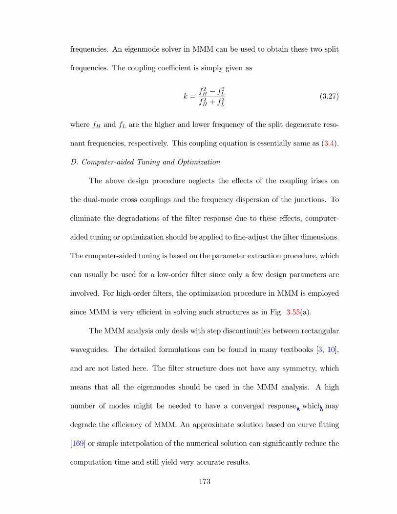
frequencies. An eigenmode solver in MMM can be used to obtain these two split
frequencies. The coupling coe¢ cient is simply given as
k =f 2H � f 2Lf 2H + f 2L
(3.27)
where fH and fL are the higher and lower frequency of the split degenerate reso-
nant frequencies, respectively. This coupling equation is essentially same as (3.4).
D. Computer-aided Tuning and Optimization
The above design procedure neglects the e¤ects of the coupling irises on
the dual-mode cross couplings and the frequency dispersion of the junctions. To
eliminate the degradations of the �lter response due to these e¤ects, computer-
aided tuning or optimization should be applied to �ne-adjust the �lter dimensions.
The computer-aided tuning is based on the parameter extraction procedure, which
can usually be used for a low-order �lter since only a few design parameters are
involved. For high-order �lters, the optimization procedure in MMM is employed
since MMM is very e¢ cient in solving such structures as in Fig. 3.55(a).
The MMM analysis only deals with step discontinuities between rectangular
waveguides. The detailed formulations can be found in many textbooks [3, 10],
and are not listed here. The �lter structure does not have any symmetry, which
means that all the eigenmodes should be used in the MMM analysis. A high
number of modes might be needed to have a converged response, which may
degrade the e¢ ciency of MMM. An approximate solution based on curve �tting
[169] or simple interpolation of the numerical solution can signi�cantly reduce the
computation time and still yield very accurate results.
173
3.6.4 Design Example
A four-pole symmetric quasi-elliptic dual-mode �lter is designed to demonstrate
the feasibility. The center frequency of the �lter is 8.5 GHz and the fractional
bandwidth is 2% (170 MHz). The normalized coupling matrix and external cou-
pling are given as
M =
266666666664
0 1:0468 0 �0:1364
1:0468 0 0:8380 0
0 0:8380 0 1:0468
�0:1364 0 1:0468 0
377777777775R = 1:3764 (3.28)
The input and output waveguide is chosen to be WR90 (a � b = 0:9 � 0:4
inch), and the width and height of the cavity waveguide are chosen to be a� a =
0:9 � 0:9 inch. In order to determine the dimensions of the input and output
irises, the two-port network structure as shown in Fig. 3.56(a) is analyzed in
MMM. The scattering parameter between the two discontinuities can be related
to the impedance inverter by (3.6). Three dimensions of the iris can be modi�ed to
obtain the desired impedance inverter: width, height and thickness. To simplify
the problem, the height of the iris is taken identical as WR90, i.e. b = 0:4 inch.
The thickness of the iris is �xed at tio = 0:1 inch. The width of iris aio is swept
to calculate the inverter values. The obtained coupling curves are shown in Fig.
3.56(b): the upper one is inverter values versus aio, and the lower ones are the
phase o¤sets versus aio. The phase o¤sets are used later to adjust the cavity
174
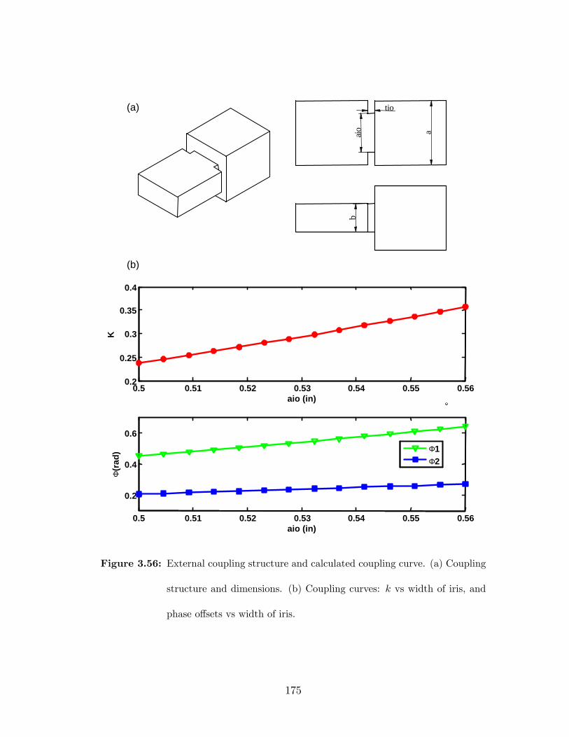
(a)
(b)
0.5 0.51 0.52 0.53 0.54 0.55 0.560.2
0.25
0.3
0.35
0.4
aio (in)
K
0.5 0.51 0.52 0.53 0.54 0.55 0.56
0.2
0.4
0.6
aio (in)
Φ(r
ad) Φ1
Φ2
0.5 0.51 0.52 0.53 0.54 0.55 0.560.2
0.25
0.3
0.35
0.4
aio (in)
K
0.5 0.51 0.52 0.53 0.54 0.55 0.56
0.2
0.4
0.6
aio (in)
Φ(r
ad) Φ1
Φ2
0.5 0.51 0.52 0.53 0.54 0.55 0.560.2
0.25
0.3
0.35
0.4
aio (in)
K
0.5 0.51 0.52 0.53 0.54 0.55 0.56
0.2
0.4
0.6
aio (in)
Φ(r
ad) Φ1
Φ2
aiob
tio
aaiob
tio
a
Figure 3.56: External coupling structure and calculated coupling curve. (a) Coupling
structure and dimensions. (b) Coupling curves: k vs width of iris, and
phase o¤sets vs width of iris.
175

length. The value of aio is decided to be 0:546 inch by interpolation to have a
desired inverter value 0:3270.
Two inter-coupling valuesM14 (or k14) andM23 (or k23) between the cavities
are provided simultaneously by the evanescent-mode iris. The scattering parame-
ters of the structure in Fig. 3.57(a) are calculated by MMM, and then related to
the inverter values. Two sets of scattering parameters need to solve: one is corre-
sponding to TE10 (H10) mode, and the other one is corresponding to TE01 (H01)
mode. Therefore, the two inverter values k14 and k23 can be computed accord-
ingly. There are three variables (width air, height bir, and thickness tir) to be
determined for an iris to realize the coupling pairs. If one variable is chosen, the
other two can be uniquely determined. Usually, the thickness of the iris is �xed
because the width and height of the iris will each mainly a¤ect one coupling value.
In this case, the thickness is �xed at tir = 0:1 inch. The width air and height bir
can be swept to calculate the inverter values k14 and k23. The obtained curves are
shown in Fig. 3.57(b). The values of air and bir are found to be 0:26 inch and
0:46 inch, respectively, to have the desired values of k14 = 0:0163 (corresponds to
H10 mode) and k23 = 0:1003 (corresponds to H01 mode). A simple optimization
procedure can also be used to �nd the values of air and bir to yield the required
couplings for a given thickness. The objective function is constructed as
err = (kc14 � kd14)2 + (kc23 � kd23)2 (3.29)
where (kc14, kc23) are the computed couplings and (k
d14, k
d23) are the desired cou-
plings.
176
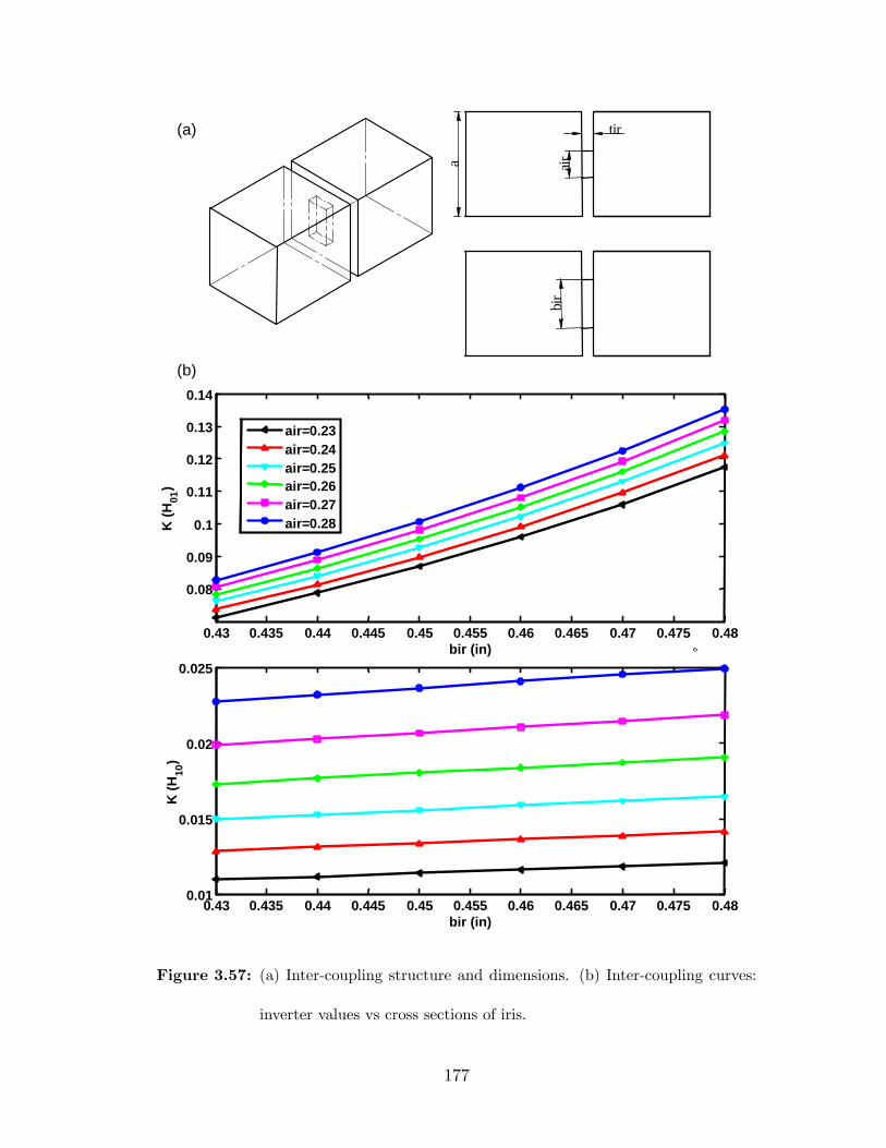
0.43 0.435 0.44 0.445 0.45 0.455 0.46 0.465 0.47 0.475 0.48
0.08
0.09
0.1
0.11
0.12
0.13
0.14
bir (in)
K (H
01)
air=0.23air=0.24air=0.25air=0.26air=0.27air=0.28
0.43 0.435 0.44 0.445 0.45 0.455 0.46 0.465 0.47 0.475 0.480.01
0.015
0.02
0.025
bir (in)
K (H
10)
0.43 0.435 0.44 0.445 0.45 0.455 0.46 0.465 0.47 0.475 0.48
0.08
0.09
0.1
0.11
0.12
0.13
0.14
bir (in)
K (H
01)
air=0.23air=0.24air=0.25air=0.26air=0.27air=0.28
0.43 0.435 0.44 0.445 0.45 0.455 0.46 0.465 0.47 0.475 0.480.01
0.015
0.43 0.435 0.44 0.445 0.45 0.455 0.46 0.465 0.47 0.475 0.48
0.08
0.09
0.1
0.11
0.12
0.13
0.14
bir (in)
K (H
01)
air=0.23air=0.24air=0.25air=0.26air=0.27air=0.28
0.43 0.435 0.44 0.445 0.45 0.455 0.46 0.465 0.47 0.475 0.480.01
0.015
0.02
0.025
bir (in)
K (H
10)
(a)
(b)
a ir
b ir
tir
a air
b ir
tir
a
Figure 3.57: (a) Inter-coupling structure and dimensions. (b) Inter-coupling curves:
inverter values vs cross sections of iris.
177
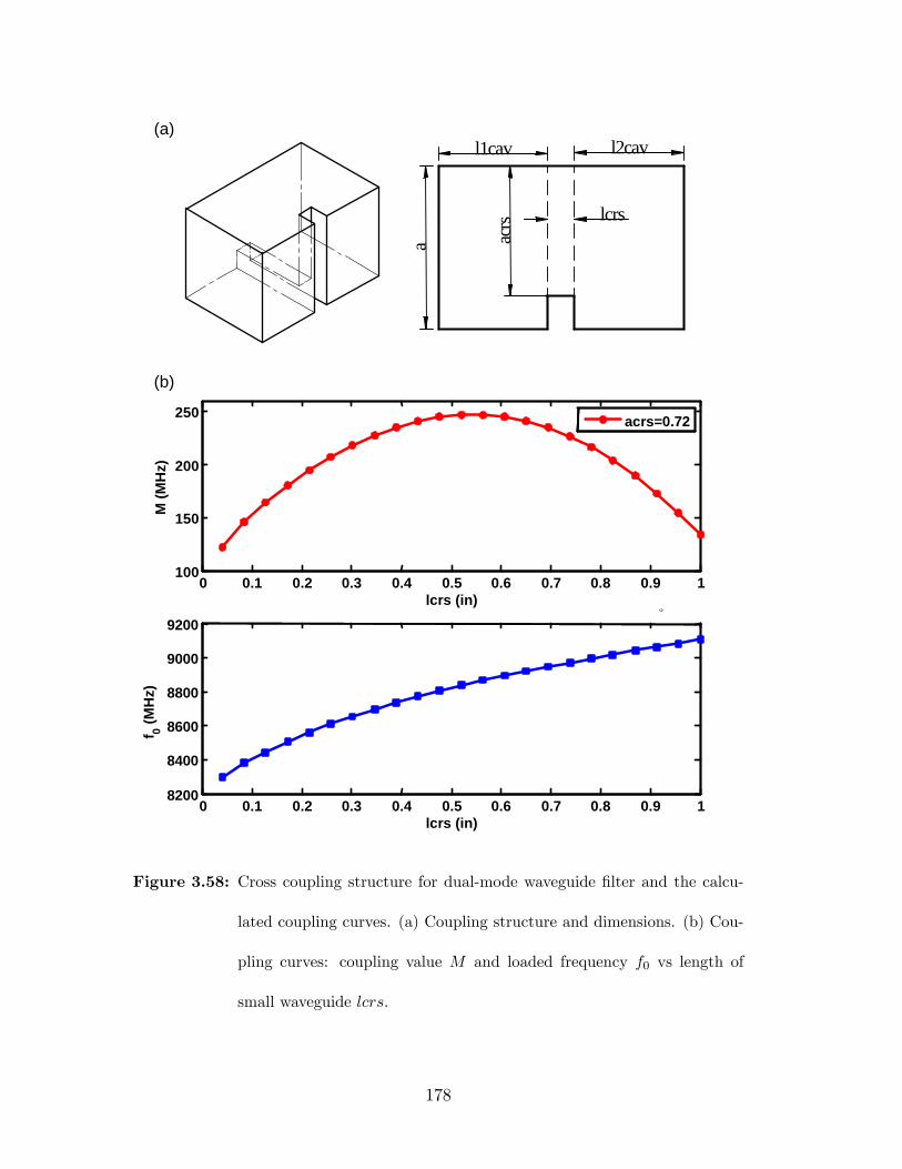
0 0.1 0.2 0.3 0.4 0.5 0.6 0.7 0.8 0.9 1100
150
200
250
lcrs (in)
M (M
Hz)
0 0.1 0.2 0.3 0.4 0.5 0.6 0.7 0.8 0.9 18200
8400
8600
8800
9000
9200
lcrs (in)
f 0(M
Hz)
acrs=0.72
0 0.1 0.2 0.3 0.4 0.5 0.6 0.7 0.8 0.9 1100
150
200
250
lcrs (in)
M (M
Hz)
0 0.1 0.2 0.3 0.4 0.5 0.6 0.7 0.8 0.9 18200
8400
8600
8800
9000
9200
lcrs (in)
f 0(M
Hz)
0 0.1 0.2 0.3 0.4 0.5 0.6 0.7 0.8 0.9 1100
150
200
250
lcrs (in)
M (M
Hz)
0 0.1 0.2 0.3 0.4 0.5 0.6 0.7 0.8 0.9 18200
8400
8600
8800
9000
9200
lcrs (in)
f 0(M
Hz)
acrs=0.72
(a)
(b)
lcrs
acr s
a
l1cav l2cav
lcrs
acr s
a
l1cav l2cav
Figure 3.58: Cross coupling structure for dual-mode waveguide �lter and the calcu-
lated coupling curves. (a) Coupling structure and dimensions. (b) Cou-
pling curves: coupling value M and loaded frequency f0 vs length of
small waveguide lcrs.
178
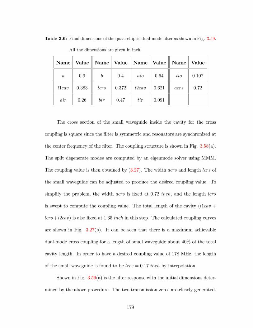
Table 3.6: Final dimensions of the quasi-elliptic dual-mode �lter as shown in Fig. 3.59.
All the dimensions are given in inch.
Name Value Name Value Name Value Name Value
a 0:9 b 0:4 aio 0:64 tio 0:107
l1cav 0:383 lcrs 0:372 l2cav 0:621 acrs 0:72
air 0:26 bir 0:47 tir 0:091
The cross section of the small waveguide inside the cavity for the cross
coupling is square since the �lter is symmetric and resonators are synchronized at
the center frequency of the �lter. The coupling structure is shown in Fig. 3.58(a).
The split degenerate modes are computed by an eigenmode solver using MMM.
The coupling value is then obtained by (3.27). The width acrs and length lcrs of
the small waveguide can be adjusted to produce the desired coupling value. To
simplify the problem, the width acrs is �xed at 0:72 inch, and the length lcrs
is swept to compute the coupling value. The total length of the cavity (l1cav +
lcrs+ l2cav) is also �xed at 1:35 inch in this step. The calculated coupling curves
are shown in Fig. 3.27(b). It can be seen that there is a maximum achievable
dual-mode cross coupling for a length of small waveguide about 40% of the total
cavity length. In order to have a desired coupling value of 178 MHz, the length
of the small waveguide is found to be lcrs = 0:17 inch by interpolation.
Shown in Fig. 3.59(a) is the �lter response with the initial dimensions deter-
mined by the above procedure. The two transmission zeros are clearly generated.
179
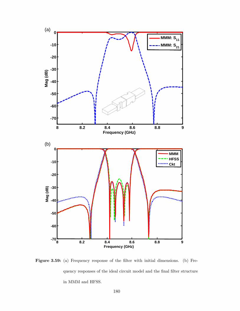
8 8.2 8.4 8.6 8.8 970
60
50
40
30
20
10
0
Frequency (GHz)
Mag
(dB
)
MMMHFSSCkt
8 8.2 8.4 8.6 8.8 970
60
50
40
30
20
10
0
Frequency (GHz)
Mag
(dB
)
MMMHFSSCkt
8 8.2 8.4 8.6 8.8 9
70
60
50
40
30
20
10
0
Mag
(dB
)
Frequency (GHz)
MMM: S11
MMM: S21
8 8.2 8.4 8.6 8.8 9
70
60
50
40
30
20
10
0
Mag
(dB
)
Frequency (GHz)
MMM: S11
MMM: S21
(a)
(b)
Figure 3.59: (a) Frequency response of the �lter with initial dimensions. (b) Fre-
quency responses of the ideal circuit model and the �nal �lter structure
in MMM and HFSS.
180
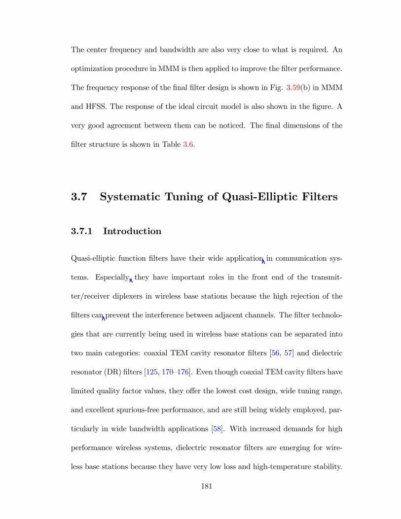
The center frequency and bandwidth are also very close to what is required. An
optimization procedure in MMM is then applied to improve the �lter performance.
The frequency response of the �nal �lter design is shown in Fig. 3.59(b) in MMM
and HFSS. The response of the ideal circuit model is also shown in the �gure. A
very good agreement between them can be noticed. The �nal dimensions of the
�lter structure is shown in Table 3.6.
3.7 Systematic Tuning of Quasi-Elliptic Filters
3.7.1 Introduction
Quasi-elliptic function �lters have their wide application in communication sys-
tems. Especially, they have important roles in the front end of the transmit-
ter/receiver diplexers in wireless base stations because the high rejection of the
�lters can prevent the interference between adjacent channels. The �lter technolo-
gies that are currently being used in wireless base stations can be separated into
two main categories: coaxial TEM cavity resonator �lters [56, 57] and dielectric
resonator (DR) �lters [125, 170�176]. Even though coaxial TEM cavity �lters have
limited quality factor values, they o¤er the lowest cost design, wide tuning range,
and excellent spurious-free performance, and are still being widely employed, par-
ticularly in wide bandwidth applications [58]. With increased demands for high
performance wireless systems, dielectric resonator �lters are emerging for wire-
less base stations because they have very low loss and high-temperature stability.
181

However, the dielectric resonator �lters have higher cost than the coaxial TEM
cavity �lters and very poor spurious performance.
Quasi-elliptic �lters using the above-mentioned two technologies usually re-
quire post-production adjustment procedure to obtain the desired �lter response
since a complete CAD of such �lters based on available numerical methods is not
possible so far. The post-production adjustment consists of two aspects: diagno-
sis and tuning. Diagnosis is to detect the components that are out of the tuning
range of the tuning screws in a manufactured �lter, e.g. one coupling value or
one cavity frequency can not be achieved by adjusting the tuning screws. Usu-
ally, these failed components must be re-manufactured or replaced. Such faults
typically originate from errors in the assembly, manufacturing, or even in the de-
sign. Tuning is to adjust and improve the �lter response by means of the tuning
screws, which often requires a skilled technician. Actually, the fault diagnosis and
tuning are closely related problems. The diagnosis and tuning of multiple-coupled
resonator quasi-elliptic �lters are usually time-consuming and expensive. They
can be very troublesome without the support of the computer. Therefore, the
development of e¢ cient algorithms for the computer aided diagnosis and tuning
becomes an essential objective in order to improve the design e¢ ciency and reduce
the cost.
Many computer aided tuning methods have been published in literatures.
Some of the algorithms are based on the optimization to extract the parameters
of the coupling matrix [122, 177]. Such algorithms rely on pre-tuned �lters whose
frequency response is su¢ ciently close to the desired response. The possibility
182

to stuck in a local minimum and fail to converge to the desired coupling matrix
is reduced. Some algorithms depend on the sensitivity analysis [178, 179]. A
nearly linear relationship between the �lter response and the depth of the tuning
screws is employed. However, in practice, this linear dependence is restricted to
small tuning ranges. Some other algorithms employing shorted circuit models do
not estimate the �lter parameters [180, 181], which make the fault diagnosis very
di¢ cult. Even though all the algorithms are based on a pre-tuned �lter, they do
not o¤er a diagnosis and tuning procedure to obtain a pre-tuned �lter from an
initially detuned �lter after manufacturing and assembling.
In this section, a systematic tuning procedure of quasi-elliptic �lters is dis-
cussed, which covers the whole process of developing a quasi-elliptic �lter from
scratch. The tuning procedure is especially useful for �lters in coaxial TEM cavi-
ties and dielectric resonators since the full-wave CAD of such �lters are not avail-
able nowadays. Filters in other technologies, e.g. waveguide and planar struc-
tures, can also be tuned on bench or in a numerical simulator based on the similar
procedure. An example of an eight-pole asymmetric dielectric resonator �lter is
presented in this section to demonstrate the whole procedure.
3.7.2 Tuning Procedure
The systematic tuning procedure presented below has been proven to be very
e¢ cient for the class of quasi-elliptic �lters using the technologies of coaxial TEM
cavities and dielectric resonators. Moreover, the principle can also be applied
183
to other realizations, in general, to all tunable �lters that can be modeled by a
coupling matrix. The systematic tuning procedure can be divided into four steps
that will be discussed next.
1. CAD of Cavity and Coupling Structures
This step is actually not a bench tuning process, but it is a very important
step to decide the manufacturing dimensions of the initial �lter structure for tun-
ing. Given the speci�cations of a �lter, a �lter topology is selected considering
the �lter performance, the mechanical feasibility and the tuning sensitivity. The
coupling matrix, which will be used for realization and tuning, is then synthesized
for this chosen �lter topology. In order to determine the mechanical dimensions
of the physical �lter structure, the �lter requirements and the coupling matrix
should be related to the mechanical structures by full-wave numerical methods.
In this step, one should try to make sure that all the �lter parameters can be
achieved by adjusting the tuning screws, in other words, all the �lter parameters
are inside the tuning range. Otherwise, post manufacturing will be required to �x
or replace some elements in the �lter, which will delay the developing time and
increase the cost.
The physical cavity dimensions are determined according to the center fre-
quency of the �lter and the desired unloaded Q factor. For coaxial TEM cavities,
the length of the cylinder rod and the capacitance loading from the tuning screw
a¤ect the resonant frequency. The size of the metallic enclosure has the in�uence
on the unloaded Q factor. For dielectric resonators, the resonant frequency is
mainly a¤ected by the size of the ceramic puck and the depth of the tuning disc.
184
The unloaded Q factor is related to the loss tangent of the dielectric material
and the size of the metallic enclosure. An eigenmode solver in MMM or FEM
can be used to design the cavity dimensions. MMM is preferred because of its
high e¢ ciency. The MMM algorithms for solving the two cavity structures can
be found in [44, 45, 154]. The tuning screw or disc should also be considered
in the eigenmode solver to check the tuning range, which is especially important
for asymmetric �lter designs. The size of the cavity enclosure can be enlarged
to improve the Q factor, however, this e¤ect becomes not apparent after some
size. Therefore, an optimum enclosure size should be determined according to the
computed Q factor and the �lter size constraint.
The dimensions of the coupling structures are decided based on the band-
width of the �lter and the desired coupling values. Two kinds of couplings are
usually required in quasi-elliptic �lters: positive and negative couplings. The �eld
distributions of the employed resonant mode of a cavity structure should be inves-
tigated, and the coupling mechanisms for positive and negative signs are created
accordingly. For coaxial TEM cavities, iris coupling structure is often used for pos-
itive or magnetic couplings, while probe structure is normally used for negative or
electric couplings [182]. For dielectric resonators, the coupling structures depend
on the employed resonant modes and the �lter topologies [57]. MMM and FEM
are mostly used to design the coupling structures for these two technologies. The
equation for computing coupling values has been presented before (p. 67). The
coupling screws should also be included in the numerical simulator, e.g. HFSS, to
make sure that the tuning range is enough to obtain the desired coupling values.
185
2. Fault Diagnosis
Filters in their initial state after manufacturing and assembling are strongly
detuned. In order to check whether all the self-coupling and mutual-coupling
values can be achieved by adjusting the tuning screws (or discs), a diagnosis
procedure should be employed. If one coupling value is found not be able to be
realized, one or more physical elements in the �lter will then need to be �xed or
replaced. The diagnosis procedure is, therefore, called fault diagnosis.
Precise parameter extraction is required to guarantee the accuracy of the
diagnosis procedure. In [183], Hsu et al presented a computer-aided diagnosis
method of cascaded (or in-line) coupled resonator �lters. Basically, the phase of
the re�ection coe¢ cient of short-circuit terminated networks is used to extract
the inter-resonator couplings and the resonant frequencies of the resonators. The
extracted parameters are always unique for the in-line coupled resonator struc-
tures. In order to apply this diagnosis method to a quasi-elliptic �lter structure,
the topology of the quasi-elliptic �lter can be separated into many in-line paths
consisting of coupled cavities. The phase responses of these one-port networks
are then measured, and the self- and mutual-coupling values can be extracted
using the method in [183]. The tuning screws are adjusted according to the
di¤erences between the extracted parameters and the desired parameters in the
pre-synthesized coupling matrix. The cavities in each path should be included
and tuned one by one according to the calculated ideal phase response to improve
the e¢ ciency. Once one or more parameters can not be achieved by the tuning
screws, the corresponding fault physical elements can be easily identi�ed.
186

In some cases, the �lter topology consists of not only in-line paths, but also
triplet or quadruplet loop paths. Most of the couplings in one loop path can be
diagnosed �rst by breaking the loop into many smaller in-line paths except one
connecting coupling. The optimization procedure can then be used to extract
the parameters of the whole loop path. Usually, the ideal phase response can be
calculated, and loaded onto the monitor of the instrument as a tuning reference.
Once the measured response is close to the ideal one, the convergence of the
optimization procedure will be guaranteed.
in the diagnosis procedure, the resonators outside the interested path must
be detuned using the tuning screws, i.e. setting the resonant frequencies of the
corresponding resonators to values outside of the frequency range under consid-
eration. The detuned resonators can create virtual short-circuit terminations at
the plane of the coupling irises or other coupling structures, which are necessary
for the applicability of the diagnosis algorithm.
3. Tuning of Sub-�lters
After the fault diagnosis procedure, all the mutual-couplings are tuned very
close to the desired coupling values, and the tuning screws have enough tuning
ranges. A sequential tuning procedure as in [121] can be applied to obtain a
pre-tuned �lter. Basically, the whole �lter is tuned gradually through the sub-
�lters, i.e. beginning with all resonators being strongly detuned, one resonator
after the other is tuned. Thus, for a �lter of degree n, one gets a sequence of
n sub-�lters, the sub-�lter i being characterized by n � i tuned and i detuned
resonators. Tuning at each step aims to minimize the deviation between the ideal
187
and actual sub-�lter response or parameters.
Usually, tuning from two ports of the �lter individually provides the possi-
bility to tune a certain number of sub-�lters using the input re�ection coe¢ cients
S11 and the remaining sub-�lters using the output re�ection coe¢ cients S22. This
increases the overall accuracy of the tuning procedure. Better performances are
obtained by minimizing the number of additional resonators to be tuned from one
port providing unperceptive variations on the phase response. These resonators
are usually coupled to other resonators by means of very weak couplings. There-
fore, a good criterion is tuning half a �lter by means of S11 and the remaining
sub-�lters by means of S22.
In practice, the ideal phase response of each sub-�lter, which can be cal-
culated using the pre-synthesized coupling matrix, can be used as a reference to
guide the tuning and improve the e¢ ciency. Usually, only the resonators need to
be tuned in this step since the mutual-couplings are already very closely tuned.
In very rare cases, if one desired sub-�lter response can not be obtained by any
means, a parameter extraction method can then be applied to determine the pa-
rameters of the corresponding tuned part of the sub-�lter, which is actually a
second diagnosis procedure. The parameter extraction of the sub-�lters is based
on the optimization procedure. The optimized parameters must be constrained
inside a small variations from the desired values, which assures that the converged
parameter values are the correct solutions.
The frequency response of the �nal sub-�lter, i.e. the whole �lter, using
the sequential tuning procedure is su¢ ciently close to the desired response. For
188

�lters of moderate degree and complexity, an additional �ne tuning procedure
even becomes unnecessary. For high degree (� 8) �lters with highly complex
topologies, the response is usually good enough for one to use the available �ne
tuning techniques.
4. Fine Tuning
The pre-tuned �lter after step 3 may require �ne tuning procedure to improve
the performance. Usually, a skilled technician can easily �nish the �ne tuning if
the pre-tuned �lter response is very close to the desired response. In some cases,
the �lter responses might be very sensitive to the parameters or the tuning screws.
Some �ne tuning techniques based on parameter extraction or space mapping can
then be employed to guide the tuning.
3.7.3 Filter Tuning Example
A quasi-elliptic eight-pole bandpass �lter realized by single TE10� mode of dielec-
tric resonators with two �nite transmission zeros in the left stopband is designed
and tuned to demonstrate the tuning procedure. The �lter possesses a center
frequency of 868.1 MHz and a fractional bandwidth of 0.86% (7.5 MHz). The
ideal �lter response is shown in Fig. 3.60, and a Cul-De-Sac topology (as the
inset of Fig. 3.60) is synthesized to ful�ll the �lter. The equal ripple frequency
point for the left stopband is at 863.95 MHz. The unloaded Q value used in the
circuit model to estimate the loss is taken as 20000 that is a typical value of the
employed dielectric resonators. This �lter is used as the transmit �lter in a trans-
189
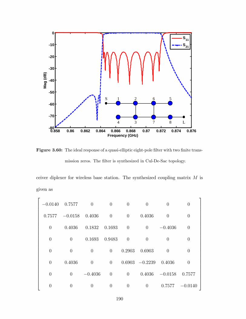
0.858 0.86 0.862 0.864 0.866 0.868 0.87 0.872 0.874 0.87680
70
60
50
40
30
20
10
0
Frequency (GHz)
Mag
(dB
)
S11
S21
0.858 0.86 0.862 0.864 0.866 0.868 0.87 0.872 0.874 0.87680
70
60
50
40
30
20
10
0
Frequency (GHz)
Mag
(dB
)
S11
S21
S 1 2
34 7 8
56
L
Figure 3.60: The ideal response of a quasi-elliptic eight-pole �lter with two �nite trans-
mission zeros. The �lter is synthesized in Cul-De-Sac topology.
ceiver diplexer for wireless base station. The synthesized coupling matrix M is
given as2666666666666666666666666664
�0:0140 0:7577 0 0 0 0 0 0
0:7577 �0:0158 0:4036 0 0 0:4036 0 0
0 0:4036 0:1832 0:1693 0 0 �0:4036 0
0 0 0:1693 0:9483 0 0 0 0
0 0 0 0 0:2903 0:6903 0 0
0 0:4036 0 0 0:6903 �0:2239 0:4036 0
0 0 �0:4036 0 0 0:4036 �0:0158 0:7577
0 0 0 0 0 0 0:7577 �0:0140
3777777777777777777777777775190
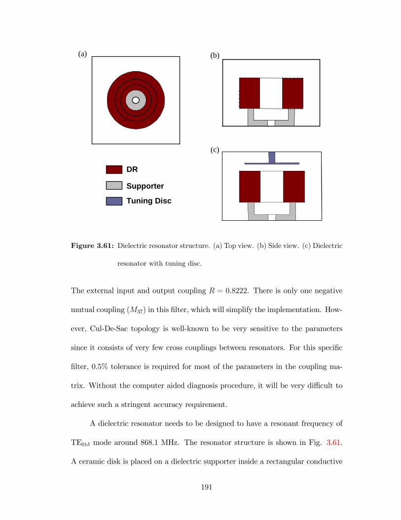
DR
Supporter
Tuning Disc
(a) (b)
(c)
Figure 3.61: Dielectric resonator structure. (a) Top view. (b) Side view. (c) Dielectric
resonator with tuning disc.
The external input and output coupling R = 0:8222. There is only one negative
mutual coupling (M37) in this �lter, which will simplify the implementation. How-
ever, Cul-De-Sac topology is well-known to be very sensitive to the parameters
since it consists of very few cross couplings between resonators. For this speci�c
�lter, 0.5% tolerance is required for most of the parameters in the coupling ma-
trix. Without the computer aided diagnosis procedure, it will be very di¢ cult to
achieve such a stringent accuracy requirement.
A dielectric resonator needs to be designed to have a resonant frequency of
TE01� mode around 868.1 MHz. The resonator structure is shown in Fig. 3.61.
A ceramic disk is placed on a dielectric supporter inside a rectangular conductive
191
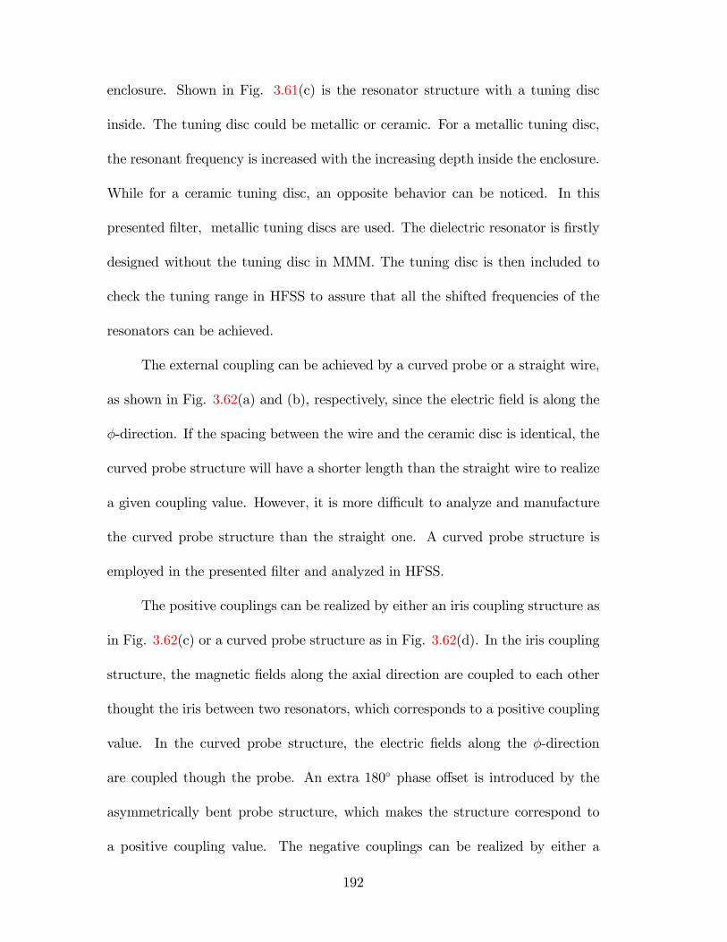
enclosure. Shown in Fig. 3.61(c) is the resonator structure with a tuning disc
inside. The tuning disc could be metallic or ceramic. For a metallic tuning disc,
the resonant frequency is increased with the increasing depth inside the enclosure.
While for a ceramic tuning disc, an opposite behavior can be noticed. In this
presented �lter, metallic tuning discs are used. The dielectric resonator is �rstly
designed without the tuning disc in MMM. The tuning disc is then included to
check the tuning range in HFSS to assure that all the shifted frequencies of the
resonators can be achieved.
The external coupling can be achieved by a curved probe or a straight wire,
as shown in Fig. 3.62(a) and (b), respectively, since the electric �eld is along the
�-direction. If the spacing between the wire and the ceramic disc is identical, the
curved probe structure will have a shorter length than the straight wire to realize
a given coupling value. However, it is more di¢ cult to analyze and manufacture
the curved probe structure than the straight one. A curved probe structure is
employed in the presented �lter and analyzed in HFSS.
The positive couplings can be realized by either an iris coupling structure as
in Fig. 3.62(c) or a curved probe structure as in Fig. 3.62(d). In the iris coupling
structure, the magnetic �elds along the axial direction are coupled to each other
thought the iris between two resonators, which corresponds to a positive coupling
value. In the curved probe structure, the electric �elds along the �-direction
are coupled though the probe. An extra 180� phase o¤set is introduced by the
asymmetrically bent probe structure, which makes the structure correspond to
a positive coupling value. The negative couplings can be realized by either a
192
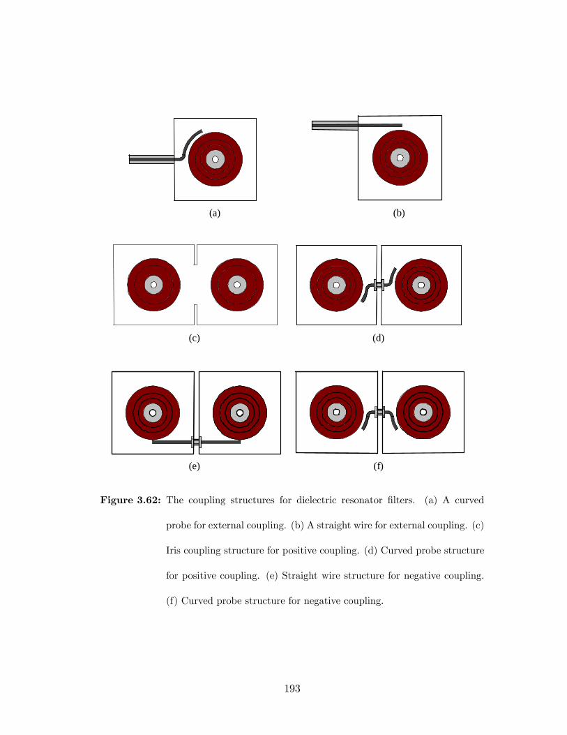
(a) (b)
(c) (d)
(e) (f)
Figure 3.62: The coupling structures for dielectric resonator �lters. (a) A curved
probe for external coupling. (b) A straight wire for external coupling. (c)
Iris coupling structure for positive coupling. (d) Curved probe structure
for positive coupling. (e) Straight wire structure for negative coupling.
(f) Curved probe structure for negative coupling.
193

straight wire as in Fig. 3.62(e) or a curved probe as in Fig. 3.62(f). Both of the
coupling structures are electric couplings. Coupling structures as in Fig. 3.62(c)
and (f) are employed in the presented �lter for the positive and negative couplings,
respectively. HFSS is used to design the dimensions for each coupling. The tuning
screws are also included in the analysis to check the tuning range. It must be
pointed out that the sign of these coupling structures might be changed for a
triplet structure because of the phase o¤set of the �eld. The detailed discussion
can be found in [170].
The �lter topology is separated into several in-line paths to perform the
diagnosis. The detailed diagnosis procedure is given as below.
1. The in-line path L-8-7-3-4 is diagnosed �rst. The probe coupling structure
for the negative coupling M37 is in this path and should be tuned at the
�rst step because the probe has very strong e¤ect on the self-couplings of
resonator 3 and 7. All the resonators are detuned at the beginning, and
added one after the other according to the order in the path. The phase
response of S22 for path L-8, L-8-7, L-8-7-3, and L-8-7-3-4 are shown in Fig.
3.63(a), (b), (c), and (d), respectively. After this step, the output coupling
and the inter-couplings between resonator 8, 7, 3 and 4 can be achieved
very accurately, and the positions of the coupling screws and probe should
be locked.
2. Continuing from step 1, resonator 4 is detuned, and path L-8-7-3-2 is di-
agnosed. The sub-path L-8-7-3 has been tuned in step 1, therefore, only
194
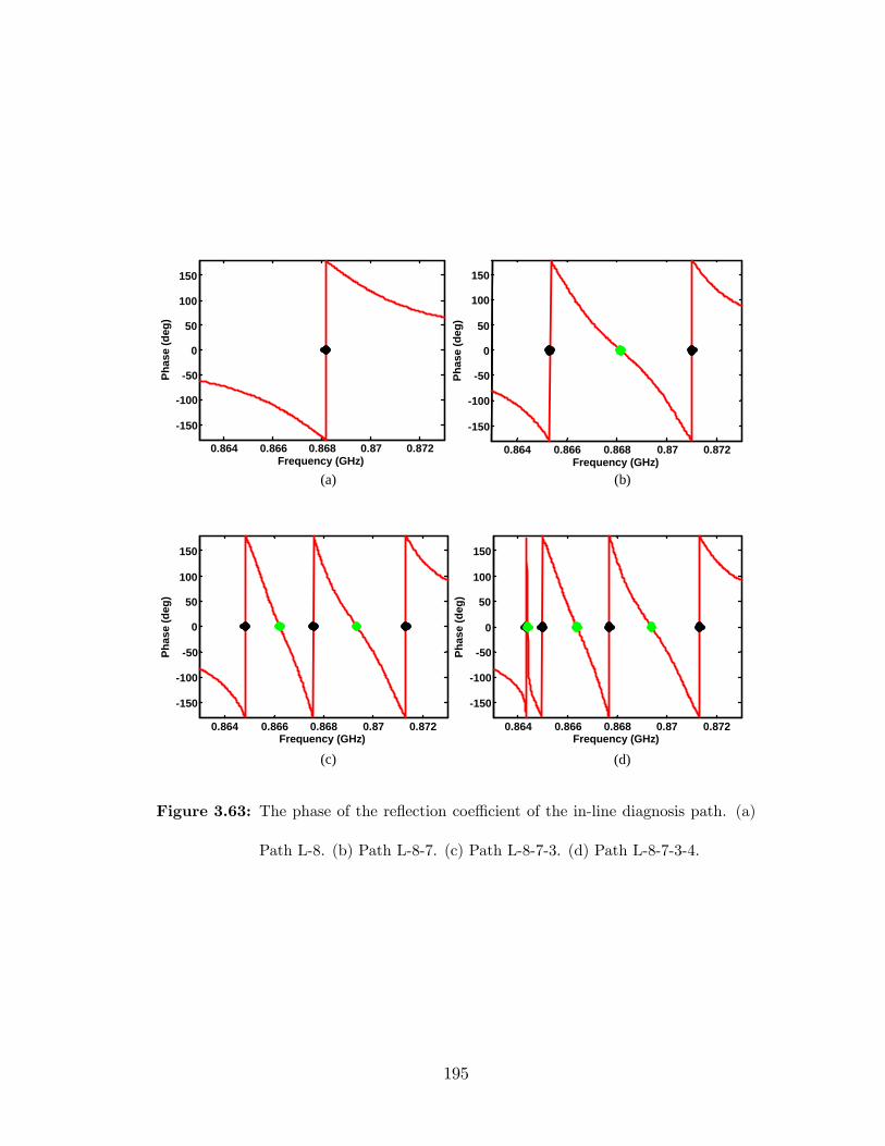
0.864 0.866 0.868 0.87 0.872
150
100
50
0
50
100
150
Frequency (GHz)
Phas
e (d
eg)
0.864 0.866 0.868 0.87 0.872
150
100
50
0
50
100
150
Frequency (GHz)
Phas
e (d
eg)
0.864 0.866 0.868 0.87 0.872
150
100
50
0
50
100
150
Frequency (GHz)Ph
ase
(deg
)0.864 0.866 0.868 0.87 0.872
150
100
50
0
50
100
150
Frequency (GHz)Ph
ase
(deg
)
(a) (b)
(c) (d)
0.864 0.866 0.868 0.87 0.872
150
100
50
0
50
100
150
Frequency (GHz)
Phas
e (d
eg)
0.864 0.866 0.868 0.87 0.872
150
100
50
0
50
100
150
Frequency (GHz)
Phas
e (d
eg)
0.864 0.866 0.868 0.87 0.872
150
100
50
0
50
100
150
Frequency (GHz)
Phas
e (d
eg)
0.864 0.866 0.868 0.87 0.872
150
100
50
0
50
100
150
Frequency (GHz)
Phas
e (d
eg)
Figure 3.63: The phase of the re�ection coe¢ cient of the in-line diagnosis path. (a)
Path L-8. (b) Path L-8-7. (c) Path L-8-7-3. (d) Path L-8-7-3-4.
195
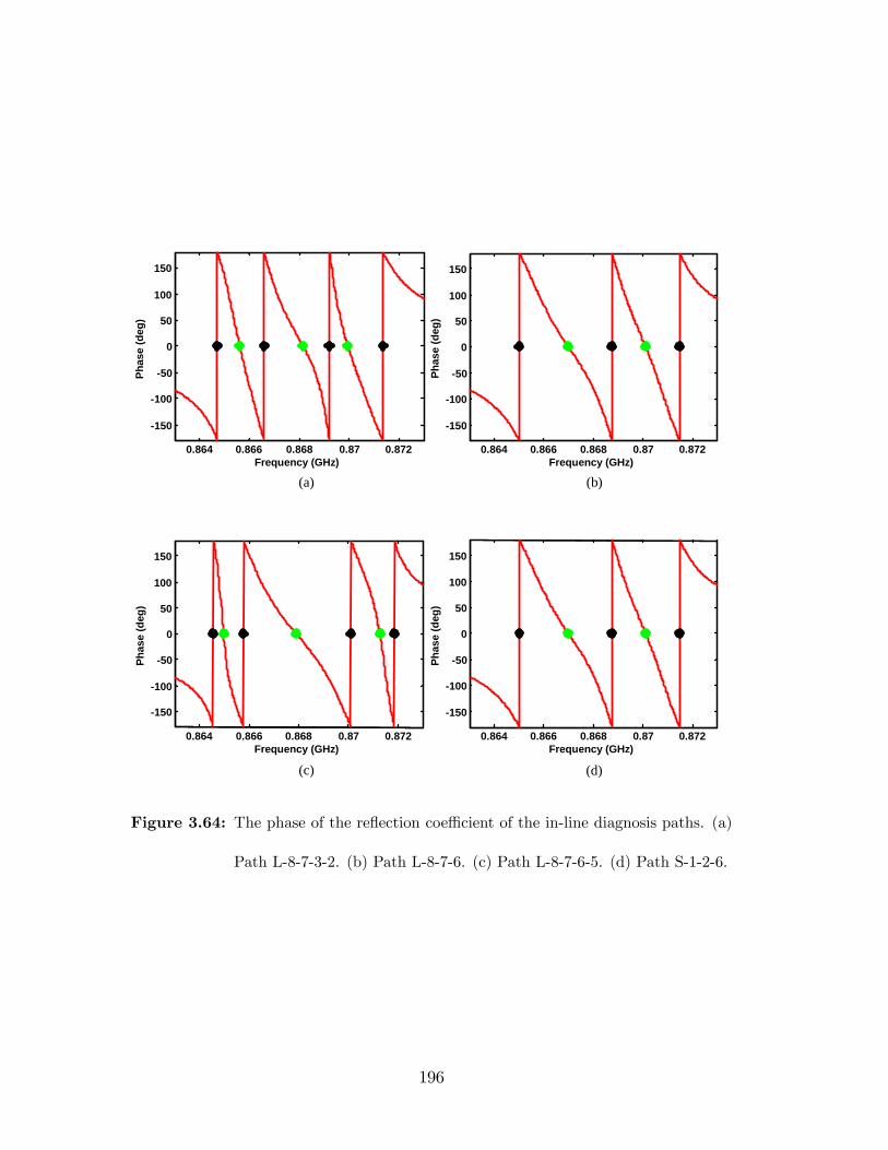
0.864 0.866 0.868 0.87 0.872
150
100
50
0
50
100
150
Frequency (GHz)
Phas
e (d
eg)
0.864 0.866 0.868 0.87 0.872
150
100
50
0
50
100
150
Frequency (GHz)
Phas
e (d
eg)
(a) (b)
(c) (d)
0.864 0.866 0.868 0.87 0.872
150
100
50
0
50
100
150
Frequency (GHz)
Phas
e (d
eg)
0.864 0.866 0.868 0.87 0.872
150
100
50
0
50
100
150
Frequency (GHz)
Phas
e (d
eg)
0.864 0.866 0.868 0.87 0.872
150
100
50
0
50
100
150
Frequency (GHz)
Phas
e (d
eg)
0.864 0.866 0.868 0.87 0.872
150
100
50
0
50
100
150
Frequency (GHz)
Phas
e (d
eg)
0.864 0.866 0.868 0.87 0.872
150
100
50
0
50
100
150
Frequency (GHz)
Phas
e (d
eg)
0.864 0.866 0.868 0.87 0.872
150
100
50
0
50
100
150
Frequency (GHz)
Phas
e (d
eg)
Figure 3.64: The phase of the re�ection coe¢ cient of the in-line diagnosis paths. (a)
Path L-8-7-3-2. (b) Path L-8-7-6. (c) Path L-8-7-6-5. (d) Path S-1-2-6.
196

coupling M23 and resonator 2 and 3 need to be tuned at this step. The
phase response of S22 for path L-8-7-3-2 is shown in Fig. 3.64(a). The
coupling M23 can be achieved very accurately after this step.
3. Continuing from step 2, resonator 2 and 3 are detuned, and path L-8-7-6-5
is diagnosed. The sub-path L-8-7 has been tuned in step 1. The resonator
6 and 5 are included one by one. The phase response of path L-8-7-6 and
L-8-7-6-5 are shown in Fig. 3.64(b) and (c), respectively. The couplings of
M67 and M56 are achieved very accurately after this step.
4. Continuing from step 3, resonator 7 and 5 are detuned, and path S-1-2-6-5
is diagnosed. The phase response of S-1 and S-1-2 are identical as L-8 and
L-8-7, respectively. The phase response of L-1-2-6 and L-1-2-6-5 are shown
in Fig. 3.64(d) and Fig. 3.64(a), respectively. The input coupling and
couplings between resonator 1, 2, and 6 can be tuned very accurately after
this step.
After the four steps of the diagnosis procedure, all the couplings in the
�lter structure are tuned very close to the desired values. A sequential tuning
procedure of the sub-�lters is then applied to align the �lter. Four sub-�lters are
tuned sequentially, namely S-1-2-6-5, S-1-2-6-5-3, S-1-2-6-5-3-4, and S-1-2-6-5-3-
4-7. The phase response of these sub-�lters are shown in Fig. 3.65. Actually, only
the resonators are needed to be tuned because all the mutual-couplings have been
achieved very close to the desired values after the diagnosis procedure.
The frequency response of the pre-tuned �lter after the sequential tuning
197
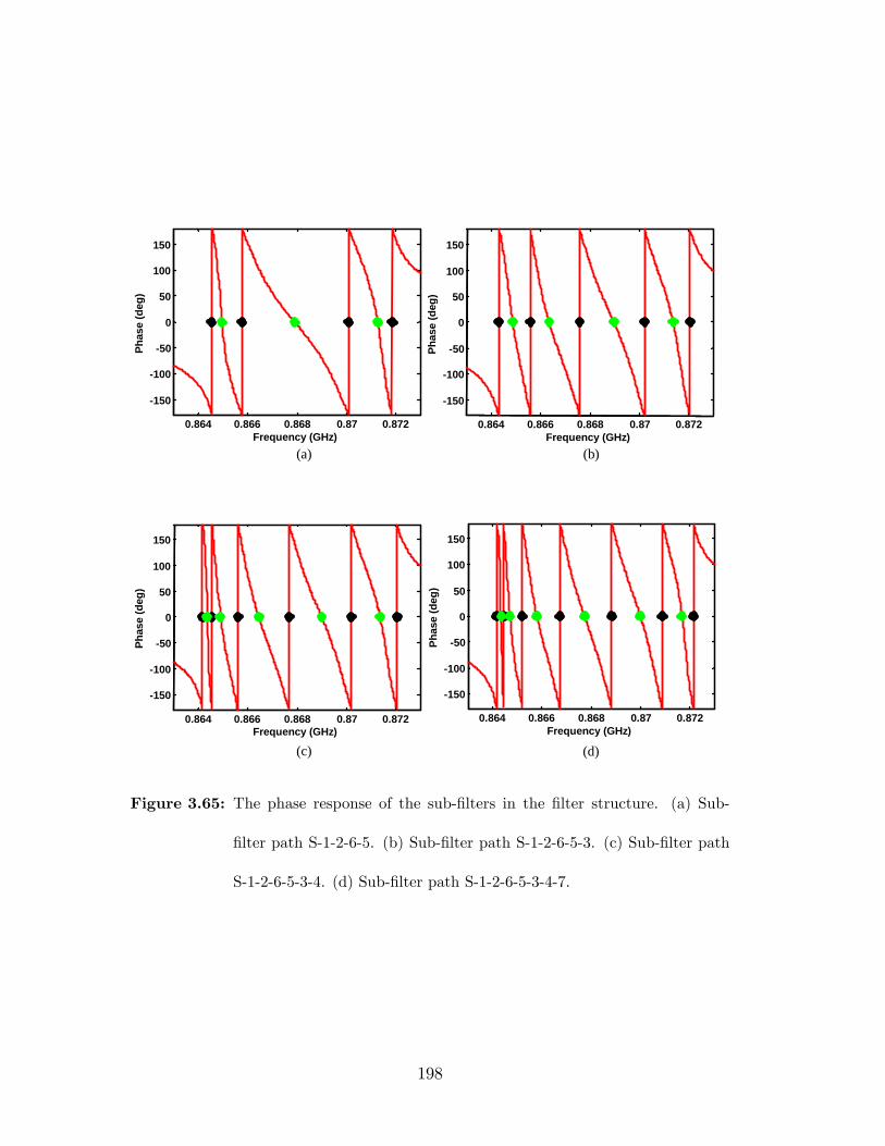
0.864 0.866 0.868 0.87 0.872
150
100
50
0
50
100
150
Frequency (GHz)
Phas
e (d
eg)
0.864 0.866 0.868 0.87 0.872
150
100
50
0
50
100
150
Frequency (GHz)
Phas
e (d
eg)
0.864 0.866 0.868 0.87 0.872
150
100
50
0
50
100
150
Frequency (GHz)
Phas
e (d
eg)
0.864 0.866 0.868 0.87 0.872
150
100
50
0
50
100
150
Frequency (GHz)
Phas
e (d
eg)
(a) (b)
(c) (d)
0.864 0.866 0.868 0.87 0.872
150
100
50
0
50
100
150
Frequency (GHz)
Phas
e (d
eg)
0.864 0.866 0.868 0.87 0.872
150
100
50
0
50
100
150
Frequency (GHz)
Phas
e (d
eg)
0.864 0.866 0.868 0.87 0.872
150
100
50
0
50
100
150
Frequency (GHz)Ph
ase
(deg
)0.864 0.866 0.868 0.87 0.872
150
100
50
0
50
100
150
Frequency (GHz)Ph
ase
(deg
)
Figure 3.65: The phase response of the sub-�lters in the �lter structure. (a) Sub-
�lter path S-1-2-6-5. (b) Sub-�lter path S-1-2-6-5-3. (c) Sub-�lter path
S-1-2-6-5-3-4. (d) Sub-�lter path S-1-2-6-5-3-4-7.
198
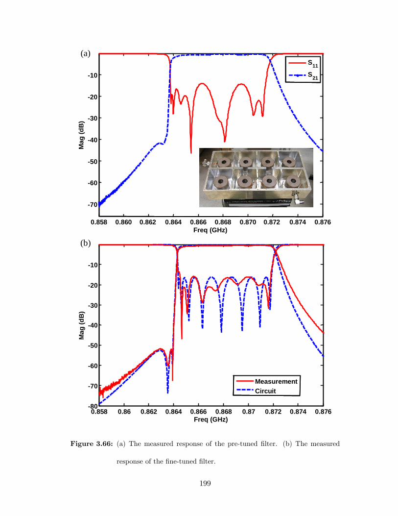
0.858 0.86 0.862 0.864 0.866 0.868 0.87 0.872 0.874 0.87680
70
60
50
40
30
20
10
Freq (GHz)
Mag
(dB
)
MeasurementCircuit
0.858 0.86 0.862 0.864 0.866 0.868 0.87 0.872 0.874 0.87680
70
60
50
40
30
20
10
Freq (GHz)
Mag
(dB
)
MeasurementCircuit
0.858 0.860 0.862 0.864 0.866 0.868 0.870 0.872 0.874 0.876
70
60
50
40
30
20
10
Freq (GHz)
Mag
(dB
)
S11
S21
0.858 0.860 0.862 0.864 0.866 0.868 0.870 0.872 0.874 0.876
70
60
50
40
30
20
10
Freq (GHz)
Mag
(dB
)
S11
S21
(a)
(b)
Figure 3.66: (a) The measured response of the pre-tuned �lter. (b) The measured
response of the �ne-tuned �lter.
199

procedure is shown in Fig. 3.66(a). The in-band response is very close to the
desired one, but the left stopband performance needs to be improved more. The
resonators 3, 4, 5 and 6, and the couplings between them are �ne tuned to improve
the �lter performance because these resonators are strongly o¤set from the center
frequency of the �lter. After several iterations, the �nal tuned �lter response is
obtained and shown in Fig. 3.66(b). The measured response is also compared
with the ideal circuit response in Fig. 3.66(b). A very good agreement can be
noticed. The physical �lter structure is shown as the inset of Fig. 3.66(a).
The presented �lter example validates the feasibility of the systematic tuning
procedure for quasi-elliptic �lters. The �lters realized in other technologies can
also be tuned in a similar procedure as the presented dielectric resonator �lter.
200

Chapter 4
Microwave Multiplexer Designs
4.1 Design Methodology
4.1.1 General Theory
The purpose of a multiplexer is to divide the frequency band into a number of
channels, which may be contiguous (adjacent in the frequency band) or separated
by guarding bands. Practical applications using multiplexers include multi-carrier
communications satellite repeater, antenna feeding system, wireless base station,
and power combiner, etc. Obviously, in order to obtain multiplexing performance
one can not just connect arbitrarily selected �lters in shunt or series and expect
the multiplexer to work. The immittance of one channel �lter might have a
seriously degrading e¤ect on the performance of the others [184]. The literature on
theories of multiplexer synthesis is quite extensive. An overview of these theories
is discussed next.
201
A fundamental multiplexer theorem was present by Grayzel [185] in 1969,
which states that it is always possible to design a contiguous multiplexer having
arbitrary bandwidths. However, the Grayzel theory is just a concept, and unsuit-
able for any practical application in its original form. In practice, two types of
multiplexers are most commonly used. One type has the property that the inter-
acting channel �lters are directly connected (all in series or all in parallel) through
a common junction without additional immittance compensation networks. The
other type is using immittance compensation networks in the multiplexer, e.g.
manifold multiplexers. For multiplexers in series or parallel form, a general direct
analytical design process is presented in [186]. Basically, independent doubly ter-
minated �lters are developed for each individual channel �rst, and formulas for
modi�cations to parameters associated with the �rst two resonators are derived to
match the multiplexer. The main limitation of these formulas is that the channels
may not be spaced too closely in frequency. In [187], an extended general design
procedure is presented for multiplexers having any number of channel �lters, with
arbitrary degrees, bandwidths, and inter-channel spacings. Commencing with the
closed-form expressions for element values in doubly terminated channel �lters,
this multiplexer design process modi�es all of the elements in each channel �lter
in turn by optimization, and preserves a match at the two points of perfect trans-
mission closes to the band edges of each channel �lter, while taking into account
the frequency dependence across each channel.
For multiplexers using immittance compensation networks, manifold mul-
tiplexers are widely used in practical applications. General design procedures of
202
manifold multiplexers can be found in [188] and [189]. Basically, the design process
also commences from doubly terminated channel �lters. The channel �lters are
connected to a manifold junction with physical separations or phase shifters in
between. The spacings or the phase shifters between channels not only serve to
separate the �lters physically, but also compensate the �lter interactions. Actu-
ally, the phase shifters are su¢ cient to compensate the multiplexer to such an
extent that contiguous channeling cases are even designable. Closed formulas and
computer optimization process can be found in [188] and [189], respectively.
When the channels of the multiplexer are contiguous, i.e. adjacent channels
have attenuation characteristics that typically cross over at 3 dB points, singly
terminated �lter prototypes are usually employed [1, 190�192]. The typical re-
sponses of the input admittance and scattering parameters of a singly terminated
quasi-elliptic �lter are shown in Fig. 4.1. The real part of the �lter input admit-
tance has an equal ripple property about the value of 1 within the passband of the
�lter, and are all zeros outside the passband (as shown in Fig 4.1(a)). Therefore,
the singly terminated �lters in a contiguous multiplexer are easier to compensate
than their doubly terminated counterpart because the condition on the input ad-
mittance of the multiplexer is more closely satis�ed by singly terminated �lters.
The condition is given by [185]
Y (s) =
nXi=1
Yi(s) = 1 =)
nXi=1
Re [Yi(s)] = 1 andnXi=1
Im [Yi(s)] = 0 (4.1)
where Y (s) is the input admittance of a contiguous multiplexer consisting of n
203
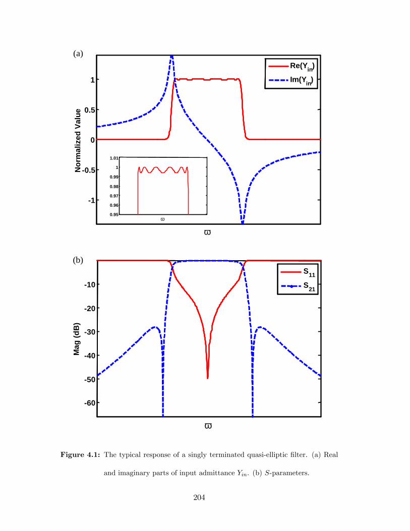
1
0.5
0
0.5
1
ω
Nor
mal
ized
Val
ueRe(Yin)
Im(Yin)
1
0.5
0
0.5
1
ω
Nor
mal
ized
Val
ueRe(Yin)
Im(Yin)
0.95
0.96
0.97
0.98
0.99
1
1.01
ω0.95
0.96
0.97
0.98
0.99
1
1.01
ω
60
50
40
30
20
10
ω
Mag
(dB
)
S11
S21
60
50
40
30
20
10
ω
Mag
(dB
)
S11
S21
(a)
(b)
Figure 4.1: The typical response of a singly terminated quasi-elliptic �lter. (a) Real
and imaginary parts of input admittance Yin. (b) S-parameters.
204
channels, and Yi(s) is the input admittance of the ith channel �lter. For mul-
tiplexer designs based on singly terminated �lters, dummy channels are usually
required to imitate absent channels at the edges of the total multiplexer band-
width, thus forming an additional annulling network for the compensation of the
channel interactions.
4.1.2 Full-Wave CAD in MMM
The above-discussed theories are based on single-mode network representations
and can only provide approximate results. It is desirable to apply rigorous nu-
merical methods for the reliable CAD of the complete multiplexer structures. In
all of the available numerical methods, MMM is well-known for its high e¢ ciency
and accuracy, and is widely employed for waveguide multiplexer designs. The an-
alyzable con�gurations and the general design procedure of multiplexers in MMM
are discussed next.
Usually, waveguide multiplexers can be decomposed as several key building
blocks, namely waveguide junctions and �lters. Possible waveguide junctions in-
clude E- and H-plane T-junctions, E- and H-plane bifurcations, E- and H-plane
multi-furcations, and ridge waveguide T-junctions, etc [3, 153]. It should be noted
that a manifold structure is actually composed of cascaded T-junctions. In some
cases, a compensation structure, e.g. a conductor block, can also be added to
these junctions to obtain better performance. Waveguide �lters might be induc-
tive window bandpass �lters, corrugated waveguide �lters, E-plane metal-insert
205
�lters [43], and ridge waveguide bandpass �lters, etc. All these key building blocks
can be analyzed in MMM by several di¤erent techniques discussed before.
The general design procedure of a multiplexer in MMM can be divided into
three main steps [3, 193, 194]. Firstly, the channel �lters are designed individually
using the techniques presented in previous chapter to meet the required speci�ca-
tions of each channel. The �lters might be doubly or singly terminated depending
on the frequency spacings between the channels. If doubly terminated �lters are
used in a multiplexer design, the stopband attenuation levels of one channel �lter
over the passbands of other channels will be improved around 6 dB after the �lter
is added to the multiplexer (due to the power division between the in-band and
out-of-band channels). This property, sometimes, can be considered to reduce
the orders of the channel �lters. After this step, all the channel �lters will be
characterized by the GSMs solved in MMM.
Secondly, the waveguide junctions are designed and analyzed in MMM. Usu-
ally, a homogeneous power splitter structure is desired for the junctions. Some
compensation structures are also often added in the junctions to have more de-
grees of freedom to match the �lter loads. The GSMs of the channel �lters are
then cascaded with the GSMs of the junctions to obtain the multiplexer response
at the initial state. A few parameters can be tuned in this step to improve the
multiplexer performance. For example, the lengths of the connecting waveguides
between �lters and junctions, and the dimensions of the compensation structures
in junctions, etc. This tuning procedure is very e¢ cient since the GSMs (nor-
mally, using the GSMs just corresponding to the fundamental modes is accurate
206
enough at this step) of the �lters (and sometimes the junctions) do not need to
be recalculated again.
The third step is a full-wave optimization procedure. A high computation
e¤ort, especially for multiplexers with many channels, is required in this step since
the whole multiplexer needs to be re-analyzed in each iteration. The parameters
to be optimized should be included gradually to speed up the convergence. Mostly,
the desired multiplexer performance can be obtained by optimizing only the �rst
few dimensions (close to the junction) in the channel �lters. In some cases, e.g. a
manifold multiplexer, if a good match has been achieved in the second step, namely
each channel can be identi�ed clearly from the multiplexer response and has an
acceptable in-band return loss for optimization, then the channel �lters can be
optimized one after the other to speed up the procedure. During the optimization
of one channel �lter, the GSMs of other components only need to be calculated
once. The dimensions of the junctions and the connecting waveguides should not
be changed during the optimization of each �lter, otherwise, the compensation
e¤ect will be destroyed. Some other techniques to improve the e¢ ciency of the
optimization procedure can be found in [195�197].
4.1.3 Hybrid CAD
For some multiplexers, the channel �lters might not possibly be analyzed by
MMM, e.g. a multiplexer consisting of a manifold junction and many dielectric
resonator �lters. The channel �lters may need to be tuned on bench or designed
207
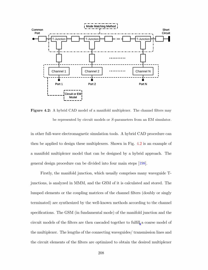
TJunction TJunction TJunction
Channel 1 Channel 2 Channel N
CommonPort
ShortCircuit
Port 1 Port 2 Port N
Circuit or EMModel
Mode Matching Method
TJunction TJunction TJunction
Channel 1 Channel 2 Channel N
CommonPort
ShortCircuit
Port 1 Port 2 Port N
Circuit or EMModel
Mode Matching Method
Figure 4.2: A hybrid CAD model of a manifold multiplexer. The channel �lters may
be represented by circuit models or S-parameters from an EM simulator.
in other full-wave electromagnetic simulation tools. A hybrid CAD procedure can
then be applied to design these multiplexers. Shown in Fig. 4.2 is an example of
a manifold multiplexer model that can be designed by a hybrid approach. The
general design procedure can be divided into four main steps [198].
Firstly, the manifold junction, which usually comprises many waveguide T-
junctions, is analyzed in MMM, and the GSM of it is calculated and stored. The
lumped elements or the coupling matrices of the channel �lters (doubly or singly
terminated) are synthesized by the well-known methods according to the channel
speci�cations. The GSM (in fundamental mode) of the manifold junction and the
circuit models of the �lters are then cascaded together to ful�ll a coarse model of
the multiplexer. The lengths of the connecting waveguides/ transmission lines and
the circuit elements of the �lters are optimized to obtain the desired multiplexer
208
performance. After the optimization, the updated circuit elements or the coupling
matrix of each channel �lter are extracted out and stored.
Secondly, each channel �lter is designed separately according to the ex-
tracted coupling matrix from the previous step (The frequency response is nor-
mally not an optimum �lter response). In this step, the �lters can be either
designed in an EM simulator or tuned on bench to match the updated �lter re-
sponse. Some special technique, like space mapping method, is often combined
with the EM tools to perform the �lter design since other numerical methods are
not so e¢ cient as MMM. After this step, the scattering parameters of each channel
�lter are obtained and stored.
Thirdly, the S-parameters of the channel �lters from the second step are
cascaded with the GSM of the manifold to check the multiplexer response (the
optimized connecting waveguide lengths from the �rst step should be used). A
second optimization procedure may be performed to improve the performance.
But this time, only the connecting waveguide lengths should be optimized. The
channel �lters may also be tuned again if the desired multiplexer performance can
not be achieved by the optimization. Therefore, it is actually an iterative process
in this step.
Fourthly, the manifold junction (also the �lters if they are designed by EM
tools in previous steps) is manufactured and assembled with the �lters to realize
the multiplexer. A �ne tuning procedure may be needed to achieve the require-
ments. Nevertheless, it usually takes a very short time if the previous steps are
successfully accomplished.
209
4.1.4 Multiport Network Synthesis
For multiplexers in an integrated structure, i.e. the complete network is formed
exclusively by coupled resonators, an exact coupling matrix synthesis method
is desired since the implementation and tuning procedure are dependent on the
coupling matrix. Many e¤orts have been made in the past on this topic [199, 200].
However, most of the approaches used today are based on optimization. Recently,
a virtually exact analytical synthesis approach was presented in [201] for diplexers.
Basically, the rational polynomials of a diplexer are obtained by an iteration
process. The polynomials for each channel �lter are then derived accordingly,
and the general method discussed in chapter 2 is used to synthesize the coupling
matrix. Another analytical method was presented in [202], in which the rational
polynomials of multiplexers are generated through the Cauchy method [203]. At
this point, the exact synthesis of multiport networks, namely multiplexers, is still
a very active research topic.
4.2 Wideband RidgeWaveguide Divider-typeMul-
tiplexers
4.2.1 Introduction
The development of millimeter-wave communications and transceiver technology
has created the need for compact, wideband, high-performance diplexers and mul-
tiplexers. Usually, waveguide multiplexers are the most suitable choices to achieve
210
these requirements. Previous waveguide multiplexer designs consist of E- and
H-plane manifold multiplexers, E- and H-plane T-junction multiplexers, E- and
H-plane divider-type multiplexers [3], and Ridge waveguide T-junction multiplex-
ers [153, 204], etc. However, rectangular waveguide junctions are usually not
applicable for wideband multiplexer designs because of the limited mono-mode
frequency range of rectangular waveguides. Ridge waveguides have much wider
mono-mode frequency range than rectangular waveguides, which makes them an
appropriate choice for wideband multiplexer designs. A wideband diplexer design
using ridge waveguide T-junction has been presented in [204]. The disadvantage
of ridge waveguide T-junction multiplexers is that the physical size, especially the
total area, is large and the physical layout makes it very di¢ cult to integrate them
inside a system.
In this section, novel ridge waveguide divider junctions are presented for
wideband multiplexer designs. A wideband match at the common port can be eas-
ily achieved for these junctions. Diplexers and multiplexers using such junctions
usually occupy a small area and provide a convenient layout for high-integration.
These diplexer or multiplexer designs are mostly applicable for LTCC applications
since they can be integrated underneath other components on a circuit board. The
LTCC realization procedure of ridge waveguide structures has been discussed be-
fore ( see sec. 3.4, p. 132). Analysis and design of the ridge waveguide divider
junctions can be completely ful�lled in MMM.
Two design examples, one diplexer and one triplexer, using ridge waveguide
divider junctions are given in this section to validate the concept. Both de-
211

signs have very wide fractional bandwidth, 95% for the diplexer and 50% for the
triplexer. Ridge waveguide evanescent-mode bandpass �lters are employed for all
the channel �lters. The diplexer and triplexer are designed to be manufactured
in LTCC technology. Multiplexer designs in metallic form using the presented
junctions are also possible.
4.2.2 Ridge Waveguide Divider Junction
Waveguide junctions are very important components in many microwave appli-
cations, especially in multiplexer designs. These junctions are usually lossless
reciprocal three ports, and all three ports can not be matched simultaneously [2].
However, in multiplexer applications, it is often desirable to have the junction
with one of its ports well matched over a wide frequency band [204], i.e. low
re�ection from the common port. Fig. 4.3(a) shows a simple ridge waveguide
divider junction. Basically, a common port of single ridge waveguide is connected
to an intermediate double ridge waveguide, and then to two separated output
ports of single ridge waveguides. Many modes, mainly the fundamental mode, of
the double ridge waveguide are excited by the fundamental mode of the common
port ridge waveguide. These modes will then excite the fundamental mode of the
two output ridge waveguides. This structure is expected to have a power divider
performance because most of the power transmitted to the double ridge waveguide
almost equally splits into the two output waveguides. The typical performance of
this simple junction structure is shown in Fig. 4.3(b), which is indeed a power
212
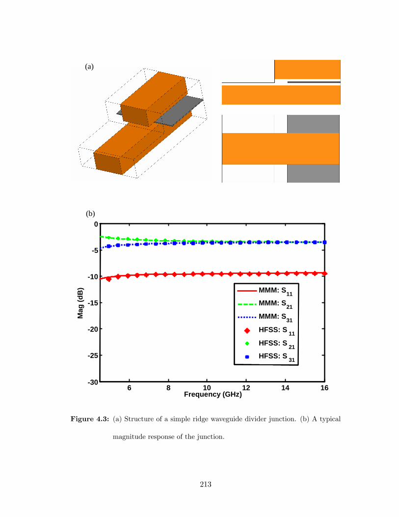
6 8 10 12 14 1630
25
20
15
10
5
0
Frequency (GHz)
Mag
(dB
) MMM: S11MMM: S21
MMM: S31
HFSS: S 11
HFSS: S 21HFSS: S 31
6 8 10 12 14 1630
25
20
15
10
5
0
Frequency (GHz)
Mag
(dB
)
6 8 10 12 14 1630
25
20
15
10
5
0
Frequency (GHz)
Mag
(dB
) MMM: S11MMM: S21
MMM: S31
HFSS: S 11
HFSS: S 21HFSS: S 31
(a)
(b)
Figure 4.3: (a) Structure of a simple ridge waveguide divider junction. (b) A typical
magnitude response of the junction.
213

divider. However, the performance of the common port matching is limited, which
is mainly due to the discontinuity between the common port ridge waveguide and
the double ridge waveguide.
In order to improve the junction performance, a matching transformer is
introduced between the common port and the double ridge waveguide. The new
junction structure is shown in Fig. 4.4(a). The transformer is used to relax
the abrupt discontinuity in the simple junction and compensate the power re�ec-
tion from the double ridge waveguide. To design a junction as in Fig. 4.4(b), an
analysis and optimization procedure by MMM is applied. The eigenmodes of each
ridge waveguide are found by the GTR technique (see Appendix A, p. 255). The
discontinuities between waveguides are characterized as GSMs solved by MMM
(using the formulations in Appendix C, p. 271). The frequency response of the
whole junction is obtained by GSM cascading. In the analysis, the three-port
junction can be represented as a generalized two-port network (see [35], p. 37),
which is convenient to cascade the junction with other channel �lters for multi-
plexer analysis. The optimization goal of the junction is to have small re�ection
coe¢ cient from the common port and almost equal transmission coe¢ cients to
the two output ports. Shown in Fig. 4.4(b) is the response of the optimized junc-
tion, which shows a very good wideband performance. Responses by HFSS are
also given in Fig. 4.3(b) and 4.4(b) to show the agreement with MMM. For both
junction structures, usually the shorter the double ridge waveguide, the better
the performance. This length can be set as the achievable minimum length of the
employed manufacture technology.
214
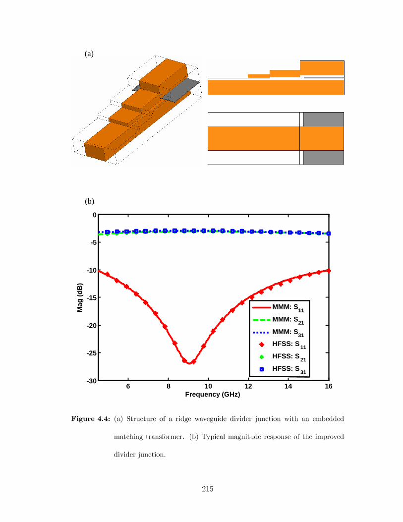
6 8 10 12 14 1630
25
20
15
10
5
0
Frequency (GHz)
Mag
(dB
)
MMM: S11
MMM: S21
MMM: S31
HFSS: S 11
HFSS: S 21
HFSS: S 31
6 8 10 12 14 1630
25
20
15
10
5
0
Frequency (GHz)
Mag
(dB
)
6 8 10 12 14 1630
25
20
15
10
5
0
Frequency (GHz)
Mag
(dB
)
MMM: S11
MMM: S21
MMM: S31
HFSS: S 11
HFSS: S 21
HFSS: S 31
(a)
(b)
Figure 4.4: (a) Structure of a ridge waveguide divider junction with an embedded
matching transformer. (b) Typical magnitude response of the improved
divider junction.
215
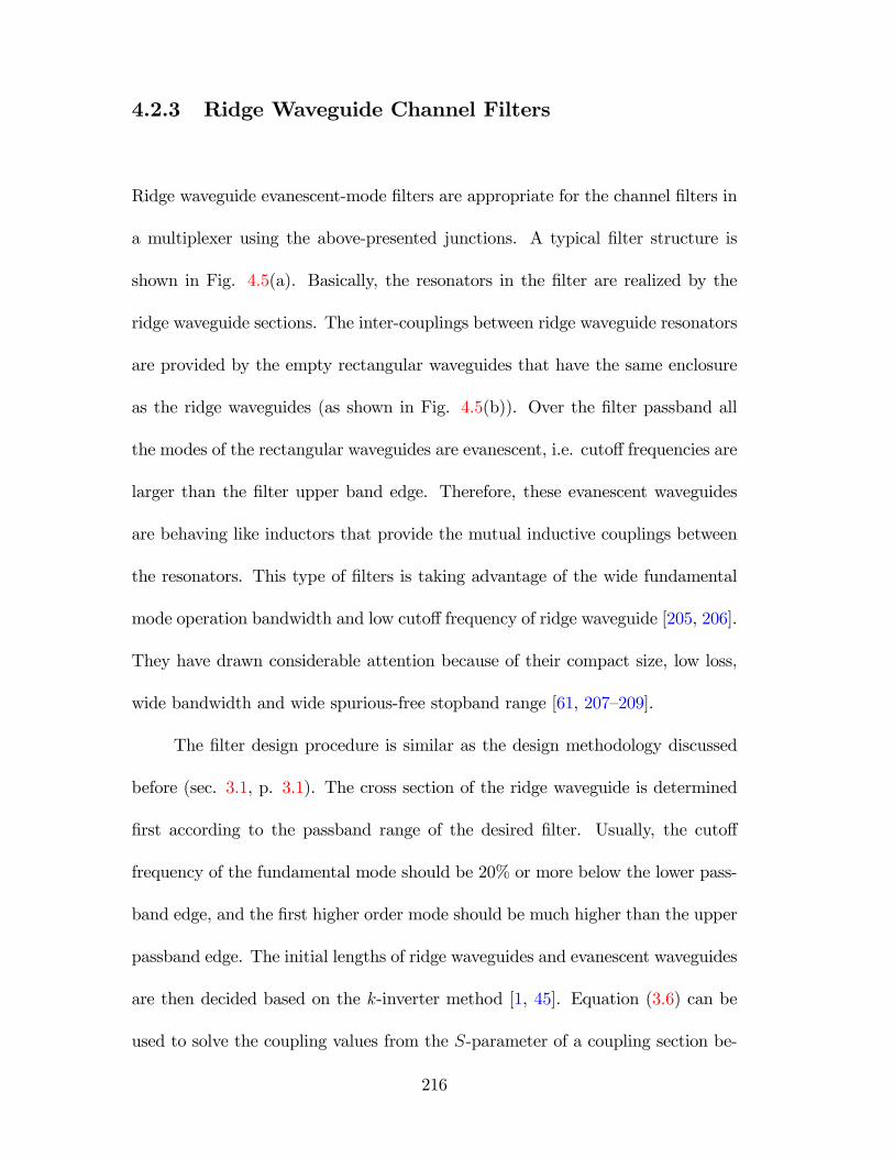
4.2.3 Ridge Waveguide Channel Filters
Ridge waveguide evanescent-mode �lters are appropriate for the channel �lters in
a multiplexer using the above-presented junctions. A typical �lter structure is
shown in Fig. 4.5(a). Basically, the resonators in the �lter are realized by the
ridge waveguide sections. The inter-couplings between ridge waveguide resonators
are provided by the empty rectangular waveguides that have the same enclosure
as the ridge waveguides (as shown in Fig. 4.5(b)). Over the �lter passband all
the modes of the rectangular waveguides are evanescent, i.e. cuto¤ frequencies are
larger than the �lter upper band edge. Therefore, these evanescent waveguides
are behaving like inductors that provide the mutual inductive couplings between
the resonators. This type of �lters is taking advantage of the wide fundamental
mode operation bandwidth and low cuto¤ frequency of ridge waveguide [205, 206].
They have drawn considerable attention because of their compact size, low loss,
wide bandwidth and wide spurious-free stopband range [61, 207�209].
The �lter design procedure is similar as the design methodology discussed
before (sec. 3.1, p. 3.1). The cross section of the ridge waveguide is determined
�rst according to the passband range of the desired �lter. Usually, the cuto¤
frequency of the fundamental mode should be 20% or more below the lower pass-
band edge, and the �rst higher order mode should be much higher than the upper
passband edge. The initial lengths of ridge waveguides and evanescent waveguides
are then decided based on the k-inverter method [1, 45]. Equation (3.6) can be
used to solve the coupling values from the S-parameter of a coupling section be-
216
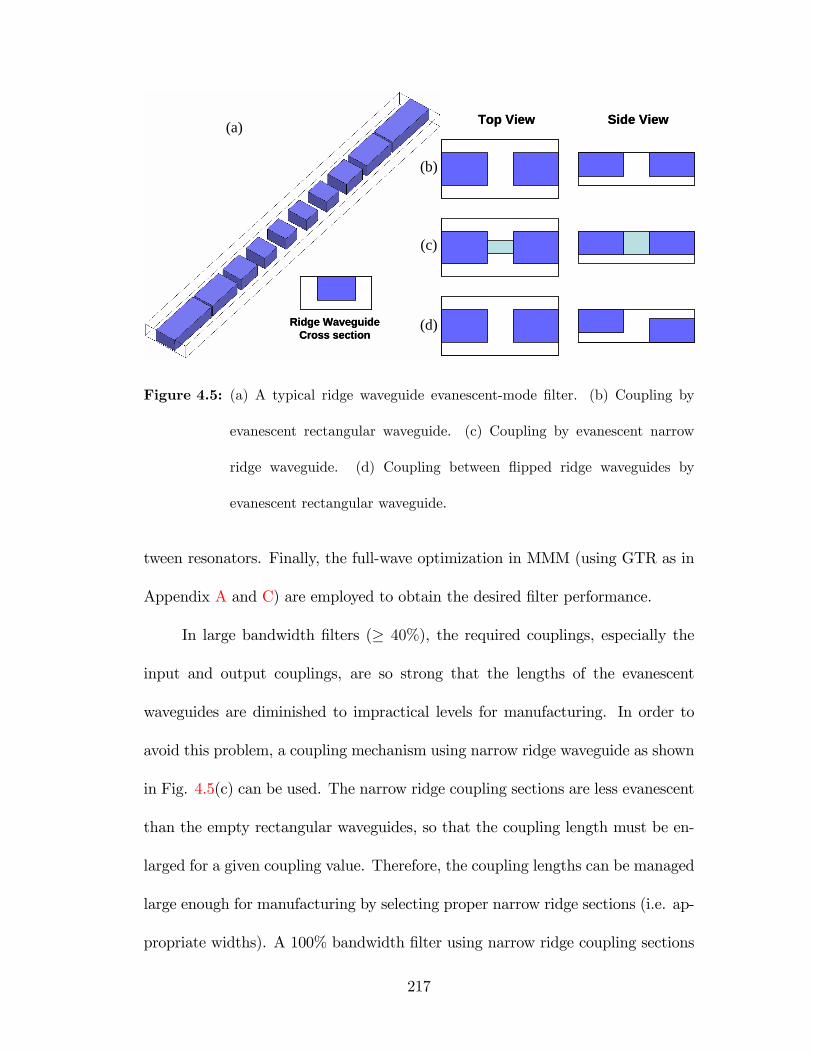
(a)
(b)
(c)
(d)Ridge WaveguideCross section
Top View Side View(a)
(b)
(c)
(d)Ridge WaveguideCross section
Ridge WaveguideCross section
Top View Side View
Figure 4.5: (a) A typical ridge waveguide evanescent-mode �lter. (b) Coupling by
evanescent rectangular waveguide. (c) Coupling by evanescent narrow
ridge waveguide. (d) Coupling between �ipped ridge waveguides by
evanescent rectangular waveguide.
tween resonators. Finally, the full-wave optimization in MMM (using GTR as in
Appendix A and C) are employed to obtain the desired �lter performance.
In large bandwidth �lters (� 40%), the required couplings, especially the
input and output couplings, are so strong that the lengths of the evanescent
waveguides are diminished to impractical levels for manufacturing. In order to
avoid this problem, a coupling mechanism using narrow ridge waveguide as shown
in Fig. 4.5(c) can be used. The narrow ridge coupling sections are less evanescent
than the empty rectangular waveguides, so that the coupling length must be en-
larged for a given coupling value. Therefore, the coupling lengths can be managed
large enough for manufacturing by selecting proper narrow ridge sections (i.e. ap-
propriate widths). A 100% bandwidth �lter using narrow ridge coupling sections
217
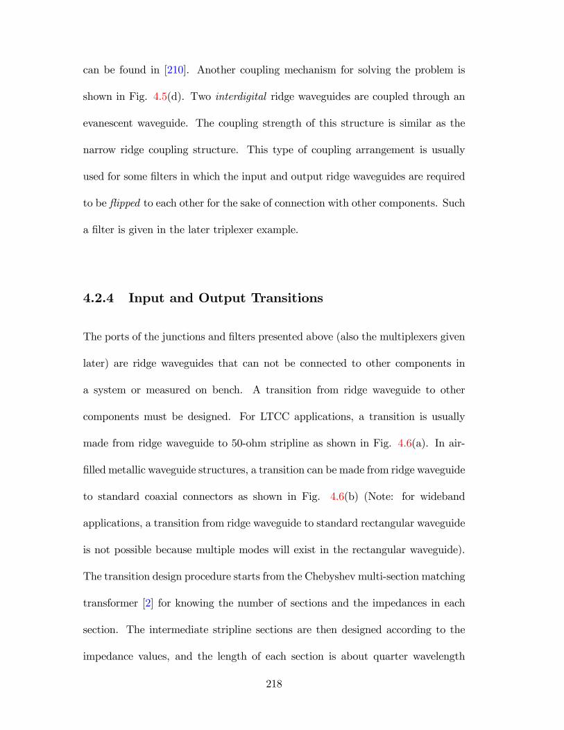
can be found in [210]. Another coupling mechanism for solving the problem is
shown in Fig. 4.5(d). Two interdigital ridge waveguides are coupled through an
evanescent waveguide. The coupling strength of this structure is similar as the
narrow ridge coupling structure. This type of coupling arrangement is usually
used for some �lters in which the input and output ridge waveguides are required
to be �ipped to each other for the sake of connection with other components. Such
a �lter is given in the later triplexer example.
4.2.4 Input and Output Transitions
The ports of the junctions and �lters presented above (also the multiplexers given
later) are ridge waveguides that can not be connected to other components in
a system or measured on bench. A transition from ridge waveguide to other
components must be designed. For LTCC applications, a transition is usually
made from ridge waveguide to 50-ohm stripline as shown in Fig. 4.6(a). In air-
�lled metallic waveguide structures, a transition can be made from ridge waveguide
to standard coaxial connectors as shown in Fig. 4.6(b) (Note: for wideband
applications, a transition from ridge waveguide to standard rectangular waveguide
is not possible because multiple modes will exist in the rectangular waveguide).
The transition design procedure starts from the Chebyshev multi-section matching
transformer [2] for knowing the number of sections and the impedances in each
section. The intermediate stripline sections are then designed according to the
impedance values, and the length of each section is about quarter wavelength
218
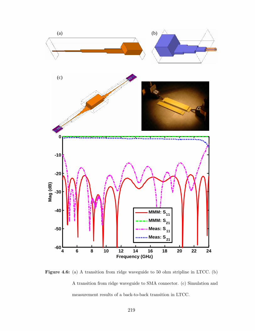
(a) (b)
4 6 8 10 12 14 16 18 20 22 2460
50
40
30
20
10
0
Mag
(dB
)
Frequency (GHz)
MMM: S11
MMM: S21Meas: S11
Meas: S21
4 6 8 10 12 14 16 18 20 22 2460
50
40
30
20
10
0
Mag
(dB
)
Frequency (GHz)
MMM: S11
MMM: S21Meas: S11
Meas: S21
(c)
Figure 4.6: (a) A transition from ridge waveguide to 50 ohm stripline in LTCC. (b)
A transition from ridge waveguide to SMA connector. (c) Simulation and
measurement results of a back-to-back transition in LTCC.
219

at the center frequency. A full-wave optimization in MMM (using GTR as in
Appendix A and C) is then applied to acquire the desired transition performance.
Extreme wideband transitions can be designed using the structures as in Fig.
4.6(a) and (b). Shown in Fig. 4.6(c) is an example of transition for LTCC appli-
cation. The fractional bandwidth is about 140% ( 4 to 24 GHz). The transition
is connected back to back, and two coplanar lines are connected to the input and
output striplines for measurement. A Cascade probe station is used to measure
the response. Even though the performance is degraded by LTCC manufacturing
e¤ect, it is still acceptable for the speci�c application.
4.2.5 Diplexer Design Example
A wideband diplexer is designed to demonstrate the feasibility of using ridge
waveguide divider junctions for multiplexer designs. The speci�cations are given
in Table 4.1. The relative bandwidth of the whole diplexer is about 95%. Channel
�lter 1 has relative bandwidth of about 31% and channel �lter 2 has about 33%.
The diplexer is designed based on LTCC technology. The relative permittivity of
dielectric material is 5.9. The thickness of each dielectric layer is 3.74 mil and the
thickness of metallization is 0.4 mil. The diplexer height must be integer multiples
of dielectric layers.
The junction as in Fig. 4.4(a) is employed for this diplexer design. Its
response as in Fig. 4.4(b) shows very good performance through the whole diplexer
frequency band.
220
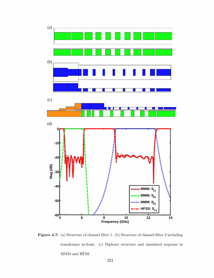
(a)
(b)
(c)
4 6 8 10 12 1460
50
40
30
20
10
0
Frequency (GHz)
Mag
(dB
)
MMM: S11
MMM: S21
MMM: S31
HFSS: S11
4 6 8 10 12 1460
50
40
30
20
10
0
Frequency (GHz)
Mag
(dB
)
MMM: S11
MMM: S21
MMM: S31
HFSS: S11
(d)
Figure 4.7: (a) Structure of channel �lter 1. (b) Structure of channel �lter 2 including
transformer in-front. (c) Diplexer structure and simulated response in
MMM and HFSS.
221
Table 4.1: The speci�cations of a wideband diplexer.
Channel Passband (GHz) Return Loss (dB) Isolation (dB)
1 4.5 �6.15 � 18 � 60
2 9.0 �12.5 � 18 � 60
Channel �lter 1 and channel �lter 2 are ridge waveguide evanescent-mode
bandpass �lters. Shown in Fig. 4.7(a) and Fig. 4.7(b) are the top and side views
of �lter 1 and �lter 2, respectively. The cross sections of the ridge waveguides
employed by these two �lters are di¤erent due to the di¤erence of the center
frequencies of the �lters. Filter 1 uses the same ridge waveguide as the junction
output waveguide, while �lter 2 uses a smaller one since it has a higher center
frequency. A matching transform is, therefore, added between the junction and
�lter 2 to connect them, which is also shown in Fig. 4.7(b). These two �lters are
initially chosen as 8-pole doubly terminated Chebyshev �lters.
Shown in Fig. 4.7(c) is the side view of the diplexer structure. The optimized
junction and channel �lters are connected together to have the initial design of the
diplexer. The response of the diplexer is computed by cascading the GSMs of the
junction and �lters (using (1.2) since the junction is characterized as a generalized
two-port network). If the higher order resonant modes of channel �lter 1 do not
exist inside the passband of channel �lter 2, the initial diplexer response (only
adjusting the connection waveguide lengths) will be a very good starting point
for optimization. If it is not the case, the higher order resonant modes of channel
222
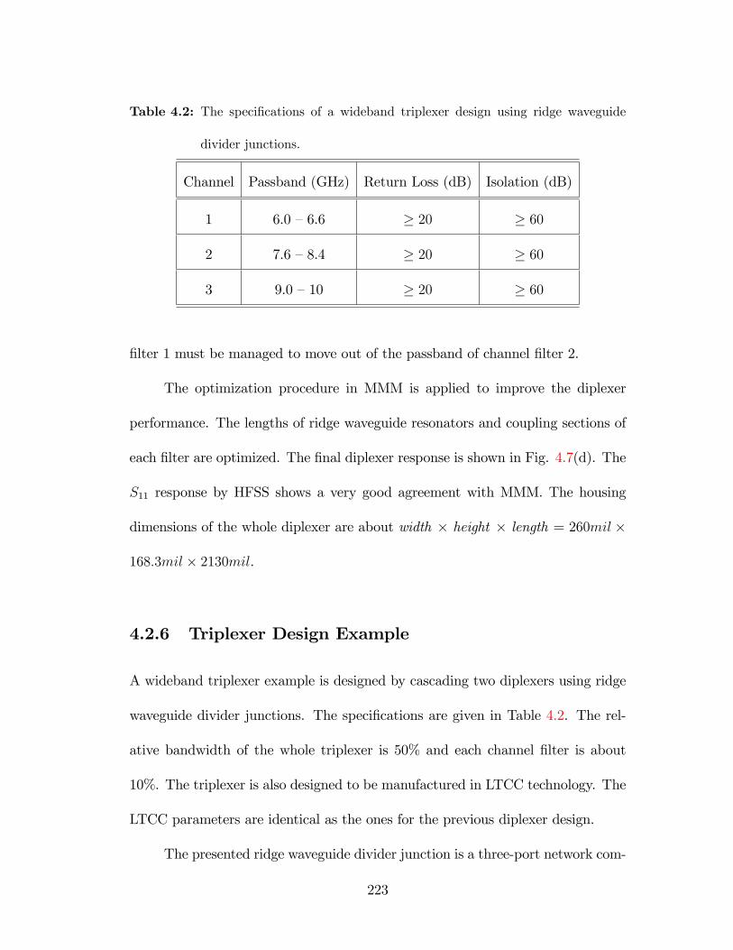
Table 4.2: The speci�cations of a wideband triplexer design using ridge waveguide
divider junctions.
Channel Passband (GHz) Return Loss (dB) Isolation (dB)
1 6.0 �6.6 � 20 � 60
2 7.6 �8.4 � 20 � 60
3 9.0 �10 � 20 � 60
�lter 1 must be managed to move out of the passband of channel �lter 2.
The optimization procedure in MMM is applied to improve the diplexer
performance. The lengths of ridge waveguide resonators and coupling sections of
each �lter are optimized. The �nal diplexer response is shown in Fig. 4.7(d). The
S11 response by HFSS shows a very good agreement with MMM. The housing
dimensions of the whole diplexer are about width � height � length = 260mil �
168:3mil � 2130mil.
4.2.6 Triplexer Design Example
A wideband triplexer example is designed by cascading two diplexers using ridge
waveguide divider junctions. The speci�cations are given in Table 4.2. The rel-
ative bandwidth of the whole triplexer is 50% and each channel �lter is about
10%. The triplexer is also designed to be manufactured in LTCC technology. The
LTCC parameters are identical as the ones for the previous diplexer design.
The presented ridge waveguide divider junction is a three-port network com-
223
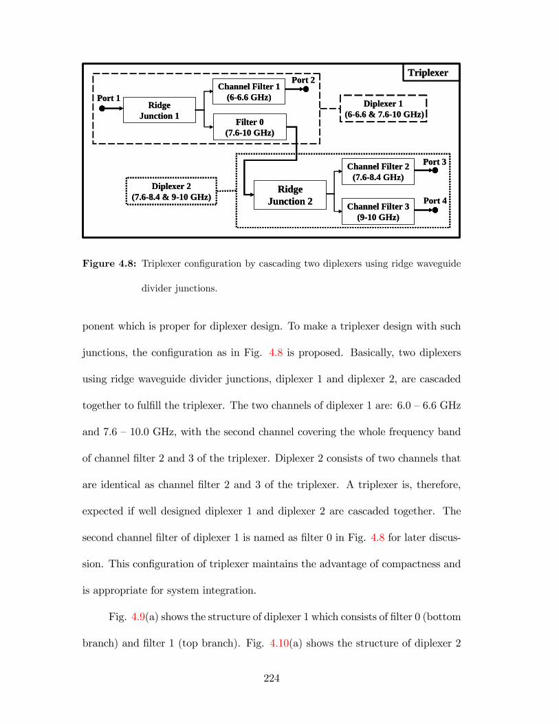
RidgeJunction 2
Channel Filter 1(66.6 GHz)
RidgeJunction 1
Channel Filter 3(910 GHz)
Channel Filter 2(7.68.4 GHz)
Port 1
Port 2
Port 3
Port 4
Filter 0(7.610 GHz)
Diplexer 1(66.6 & 7.610 GHz)
Diplexer 2(7.68.4 & 910 GHz)
Triplexer
RidgeJunction 2
Channel Filter 1(66.6 GHz)
RidgeJunction 1
Channel Filter 3(910 GHz)
Channel Filter 2(7.68.4 GHz)
Port 1
Port 2
Port 3
Port 4
Filter 0(7.610 GHz)
Diplexer 1(66.6 & 7.610 GHz)
Diplexer 2(7.68.4 & 910 GHz)
Triplexer
Figure 4.8: Triplexer con�guration by cascading two diplexers using ridge waveguide
divider junctions.
ponent which is proper for diplexer design. To make a triplexer design with such
junctions, the con�guration as in Fig. 4.8 is proposed. Basically, two diplexers
using ridge waveguide divider junctions, diplexer 1 and diplexer 2, are cascaded
together to ful�ll the triplexer. The two channels of diplexer 1 are: 6.0 �6.6 GHz
and 7.6 �10.0 GHz, with the second channel covering the whole frequency band
of channel �lter 2 and 3 of the triplexer. Diplexer 2 consists of two channels that
are identical as channel �lter 2 and 3 of the triplexer. A triplexer is, therefore,
expected if well designed diplexer 1 and diplexer 2 are cascaded together. The
second channel �lter of diplexer 1 is named as �lter 0 in Fig. 4.8 for later discus-
sion. This con�guration of triplexer maintains the advantage of compactness and
is appropriate for system integration.
Fig. 4.9(a) shows the structure of diplexer 1 which consists of �lter 0 (bottom
branch) and �lter 1 (top branch). Fig. 4.10(a) shows the structure of diplexer 2
224
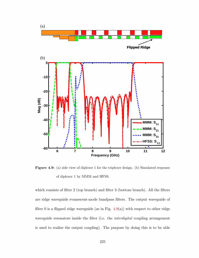
Flipped RidgeFlipped Ridge
6 7 8 9 10 11 1260
50
40
30
20
10
0
Frequency (GHz)
Mag
(dB
)
MMM: S11
MMM: S21
MMM: S31
HFSS: S11
6 7 8 9 10 11 1260
50
40
30
20
10
0
Frequency (GHz)
Mag
(dB
)
MMM: S11
MMM: S21
MMM: S31
HFSS: S11
(a)
(b)
Figure 4.9: (a) side view of diplexer 1 for the triplexer design. (b) Simulated response
of diplexer 1 by MMM and HFSS.
which consists of �lter 2 (top branch) and �lter 3 (bottom branch). All the �lters
are ridge waveguide evanescent-mode bandpass �lters. The output waveguide of
�lter 0 is a �ipped ridge waveguide (as in Fig. 4.9(a)) with respect to other ridge
waveguide resonators inside the �lter (i.e. the interdigital coupling arrangement
is used to realize the output coupling). The purpose by doing this is to be able
225
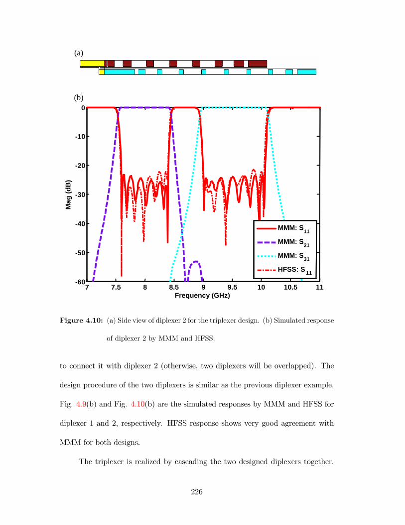
7 7.5 8 8.5 9 9.5 10 10.5 1160
50
40
30
20
10
0
Frequency (GHz)
Mag
(dB
)
MMM: S11
MMM: S21
MMM: S31
HFSS: S11
7 7.5 8 8.5 9 9.5 10 10.5 1160
50
40
30
20
10
0
Frequency (GHz)
Mag
(dB
)
MMM: S11
MMM: S21
MMM: S31
HFSS: S11
(a)
(b)
Figure 4.10: (a) Side view of diplexer 2 for the triplexer design. (b) Simulated response
of diplexer 2 by MMM and HFSS.
to connect it with diplexer 2 (otherwise, two diplexers will be overlapped). The
design procedure of the two diplexers is similar as the previous diplexer example.
Fig. 4.9(b) and Fig. 4.10(b) are the simulated responses by MMM and HFSS for
diplexer 1 and 2, respectively. HFSS response shows very good agreement with
MMM for both designs.
The triplexer is realized by cascading the two designed diplexers together.
226
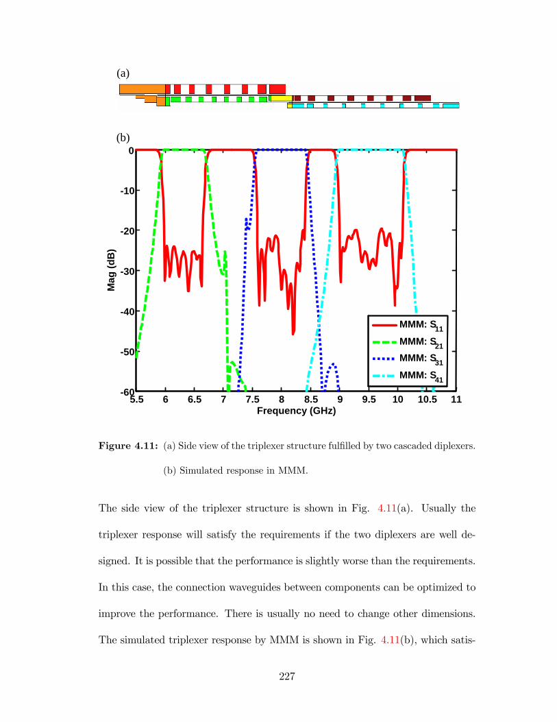
5.5 6 6.5 7 7.5 8 8.5 9 9.5 10 10.5 1160
50
40
30
20
10
0
Frequency (GHz)
Mag
(dB
)
MMM: S11
MMM: S21MMM: S31
MMM: S41
5.5 6 6.5 7 7.5 8 8.5 9 9.5 10 10.5 1160
50
40
30
20
10
0
Frequency (GHz)
Mag
(dB
)
MMM: S11
MMM: S21MMM: S31
MMM: S41
(a)
(b)
Figure 4.11: (a) Side view of the triplexer structure ful�lled by two cascaded diplexers.
(b) Simulated response in MMM.
The side view of the triplexer structure is shown in Fig. 4.11(a). Usually the
triplexer response will satisfy the requirements if the two diplexers are well de-
signed. It is possible that the performance is slightly worse than the requirements.
In this case, the connection waveguides between components can be optimized to
improve the performance. There is usually no need to change other dimensions.
The simulated triplexer response by MMM is shown in Fig. 4.11(b), which satis-
227
�es all the desired requirements. The housing dimensions of the whole triplexer
are about:width � height � length = 200mil � 149:6mil � 4276mil.
4.3 Waveguide Multiplexers for Space Applica-
tions
4.3.1 Introduction
Multiplexers for space applications, e.g. satellite payload system, are desired to
have good performance in four aspects. Firstly, the lowest possible insertion loss
is desired in each channel �lter, especially in the transmitting channel, to obtain
optimal e¢ ciency with the limited power of the spacecraft or satellite. Secondly,
The lowest possible mass and compact size are sought due to the high launch
cost of a payload. Thirdly, the highest possible power handling capability is
aimed in order to include more carriers in the transmitting channel and avoid the
multipaction discharge. Fourthly, the largest possible working temperature range
is wanted to overcome the severe environmental condition in space. In order to
achieve an optimum solution concerning these decisive deign goals, the manifold
multiplexing technique is most commonly used [3].
A modern satellite payload system usually requires three di¤erent type of
multiplexers: the diplexing or multiplexing antenna feed system, the input mul-
tiplexer (IMUX) to split the carriers into the power ampli�ers (usually traveling
wave tubes), and the output multiplexer (OMUX) to combine the carriers into the
228
transmitting channel. In this section, the diplexer and multiplexer for antenna
feed system are discussed and designed. In order to limit the experimental ex-
pense, a complete CAD procedure is employed to design these multiplexers with
the considerations of insertion loss, mass and volume, multipaction e¤ect, and
temperature drifting. More importantly, the manufacturing tolerance has been
taken into account at the design step, and therefore, the designed multiplexers
need not be tuned after the manufacture.
Two frequency bands are normally used in satellite TV system: C band
and Ku band. In this section, two multiplexers at the Ku band are designed
for the antenna feeding in a satellite payload system that is used to receive the
uplink signal and transmit the ampli�ed downlink signal. The complete design
procedure and necessary considerations related to the above-mentioned design
goals are demonstrated through these two multiplexer examples.
4.3.2 Multiplexer Con�guration and Modeling
Metallic waveguides are used in the multiplexer structures in order to achieve low
insertion loss and high power handling capability. Waveguide E-plane T-junctions
as shown in Fig. 4.12(a) are employed to ful�ll a manifold and connect the channel
�lters. Compared with the typical manifold multiplexer, the multiplexers in this
section use a slightly di¤erent con�guration as shown in Fig. 4.12(b). The channel
�lters are sequentially connected to the T-junctions of the manifold according
to their center frequencies. Instead of a short circuit at the opposite end of
229
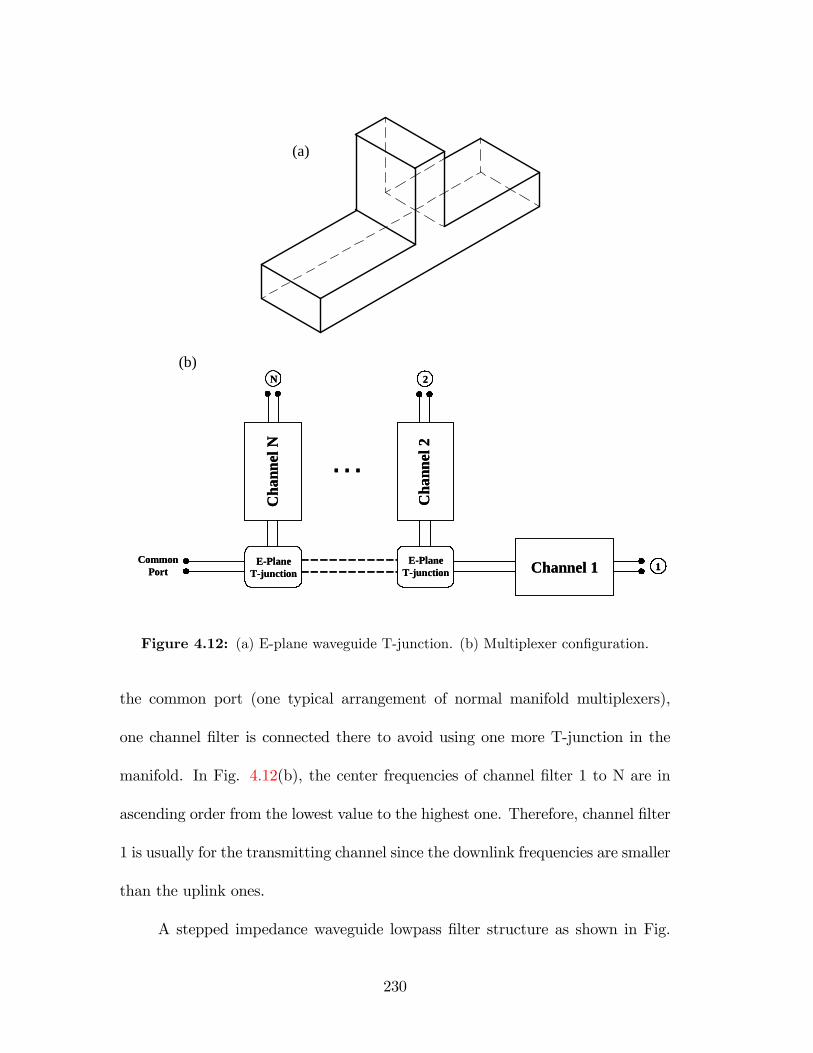
EPlaneTjunction
Cha
nnel
N
Cha
nnel
2
Channel 1EPlaneTjunction
CommonPort 1
2N
…
EPlaneTjunction
Cha
nnel
N
Cha
nnel
2
Channel 1EPlaneTjunction
CommonPort 11
2N
…
(a)
(b)
Figure 4.12: (a) E-plane waveguide T-junction. (b) Multiplexer con�guration.
the common port (one typical arrangement of normal manifold multiplexers),
one channel �lter is connected there to avoid using one more T-junction in the
manifold. In Fig. 4.12(b), the center frequencies of channel �lter 1 to N are in
ascending order from the lowest value to the highest one. Therefore, channel �lter
1 is usually for the transmitting channel since the downlink frequencies are smaller
than the uplink ones.
A stepped impedance waveguide lowpass �lter structure as shown in Fig.
230
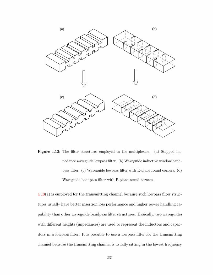
(a)
(c)
(b)
(d)
Figure 4.13: The �lter structures employed in the multiplexers. (a) Stepped im-
pedance waveguide lowpass �lter. (b) Waveguide inductive window band-
pass �lter. (c) Waveguide lowpass �lter with E-plane round corners. (d)
Waveguide bandpass �lter with E-plane round corners.
4.13(a) is employed for the transmitting channel because such lowpass �lter struc-
tures usually have better insertion loss performance and higher power handling ca-
pability than other waveguide bandpass �lter structures. Basically, two waveguides
with di¤erent heights (impedances) are used to represent the inductors and capac-
itors in a lowpass �lter. It is possible to use a lowpass �lter for the transmitting
channel because the transmitting channel is usually sitting in the lowest frequency
231

range of a multiplexer. An inductive window waveguide bandpass �lter structure
as shown in Fig. 4.13(b) is used for the receiving channels in a multiplexer. Ba-
sically, waveguide resonators are coupled through the iris windows in between
[1].
The multiplexers using the E-plane T-junctions and the two types of �l-
ter structures can be manufactured as one integrated element by the split-block
housing fabrication procedure, i.e. the whole multiplexer structure is split into
two halves along the symmetric plane (magnetic wall). The multiplexers are ex-
pected to operating correctly right after the manufacturing, which means that
tuning screws are not needed in the physical structures. However, in reality, the
round corners resulting from the manufacturing process are not avoidable due to
the �nite tool radius. This corner problem is not serious for multiplexers at low
frequency bands, but it becomes critical as the operating frequency band moves
to millimeter-wave frequency, e.g. Ku band in this section, since the dimensions
of the multiplexers are now comparable with the round corners. To overcome this
corner problem, modi�ed �lter structures, as shown in Fig. 4.13(c) and (d), are
used instead of the ideal ones as in Fig. 4.13(a) and (b). In the two modi�ed �lter
structures, E-plane round corners are included in the designs. The performance of
manufactured multiplexers using such modi�ed �lters can be maintained almost
identical as the designed one. The modi�ed �lters also allow the use of relatively
large radius tools, which can reduce the manufacturing di¢ culty and lower the
cost.
The E-plane T-junction can be modeled in MMM using either the three-
232
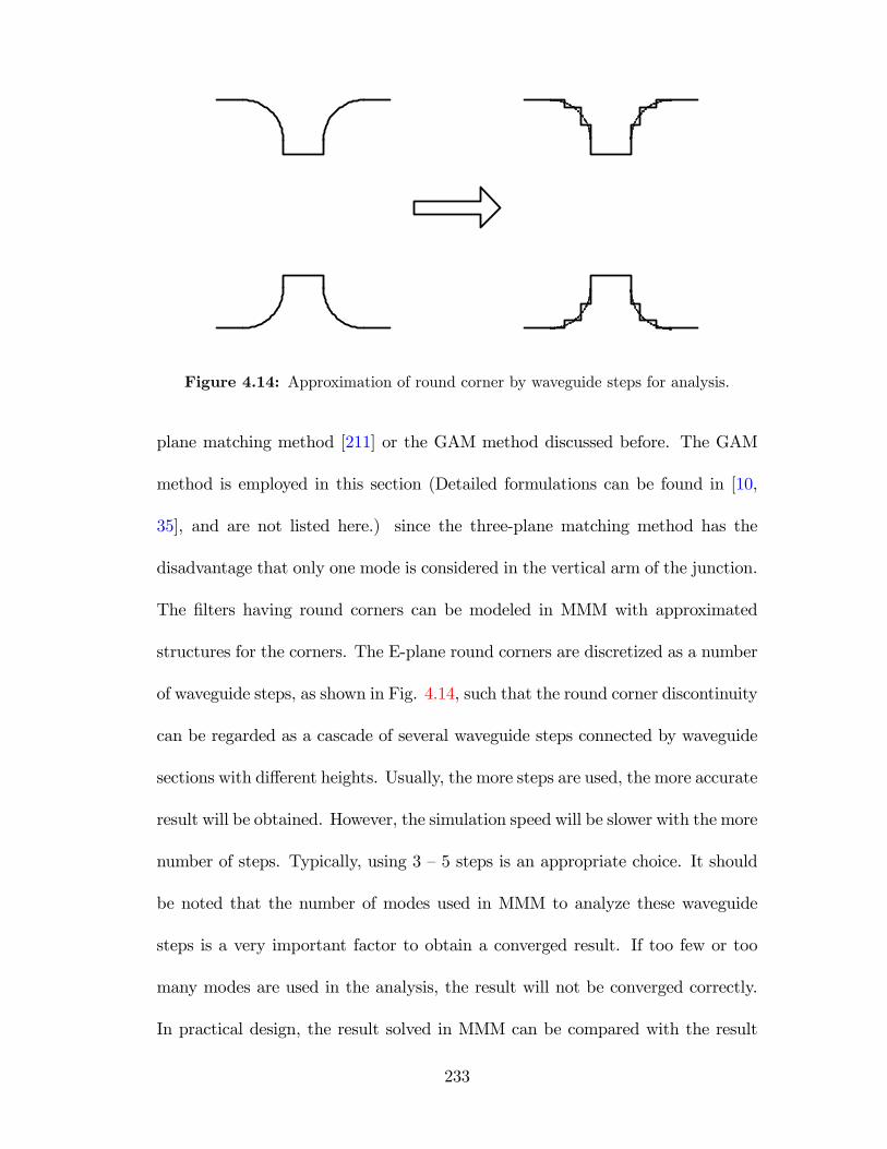
Figure 4.14: Approximation of round corner by waveguide steps for analysis.
plane matching method [211] or the GAM method discussed before. The GAM
method is employed in this section (Detailed formulations can be found in [10,
35], and are not listed here.) since the three-plane matching method has the
disadvantage that only one mode is considered in the vertical arm of the junction.
The �lters having round corners can be modeled in MMM with approximated
structures for the corners. The E-plane round corners are discretized as a number
of waveguide steps, as shown in Fig. 4.14, such that the round corner discontinuity
can be regarded as a cascade of several waveguide steps connected by waveguide
sections with di¤erent heights. Usually, the more steps are used, the more accurate
result will be obtained. However, the simulation speed will be slower with the more
number of steps. Typically, using 3 �5 steps is an appropriate choice. It should
be noted that the number of modes used in MMM to analyze these waveguide
steps is a very important factor to obtain a converged result. If too few or too
many modes are used in the analysis, the result will not be converged correctly.
In practical design, the result solved in MMM can be compared with the result
233
from other numerical methods, e.g. HFSS, and the number of modes employed in
MMM can be determined accordingly. The formulations used in MMM program
for a waveguide step discontinuity can be found in [3, 10, 35].
The lowpass �lter is designed using the stepped-impedance lowpass �lter
theory [2]. The port waveguide dimensions, width a0 and height b0, are decided
�rst according to the operating frequency range and the interface to other com-
ponents. The height dimensions, bh and bl, of the high-z and low-z waveguides
(they have the same width as the port waveguide) are then determined based on
the power handling consideration and the stopband rejection requirement. The
initial lengths of the waveguides are given as
lh =Lb0�hbh
and ll =Cbl�lb0
(4.2)
where L and C are the inductances and capacitances in the circuit model of the
lowpass �lter, respectively. lh and ll are the corresponding lengths of the high-z
and low-z waveguides. �g, g = (h; l), is the propagating constant of the waveguide
at the cuto¤ frequency f0 of the lowpass �lter, which is given as
�g =2�qf 20 � f 2c;gc
(4.3)
where fc;g is the cuto¤ frequency of the fundamental mode of the waveguides. c
is the speed of light in vacuum. Finally, the optimization procedure in MMM is
applied to acquire the desired �lter performance. Once round corners are included
in the lowpass �lter, the frequency response will be shifted slightly higher. The
lengths of the high-z waveguides can be tuned longer to compensate the shifting
e¤ect. A second optimization procedure may be needed too.
234
The bandpass �lter is designed based on the k-inverter method [1]. The
round corner approximated by the waveguide steps should be included in the
MMM analysis to calculate the inverter values. Optimization is also required
to improve the �lter performance. The analysis and optimization of the whole
multiplexer in MMM have been discussed before, and are ignored here.
4.3.3 Multipaction Consideration
The transmitting �lter in a multiplexer can su¤er malfunctions if multipaction
discharges are present during its life cycle. Multipaction discharge is a resonant
vacuum discharge which is actually an avalanche caused by secondary electron
emission [212, 213]. Primary electrons accelerated by microwave �elds can impact
a surface and release a larger number of secondary electrons, which may in turn
be accelerated and impact a surface again to release even more electrons. Hence,
a resonant discharge occurs. Multipaction phenomena can dissipate substantial
amounts of energy fed into microwave structures. It can detune a microwave signal
and heat the surface, possibly increasing noise levels and perhaps causing damage.
In some circumstances, multipaction may even induce vacuum breakdown. For
satellite application, a multipaction discharge can lead to a failure in the whole
satellite transponder. The space hardware, e.g. multiplexer in this section, needs
to be extensively tested against multipaction before launch, which is usually a
very expensive task. Sometimes, a device may have to be redesigned and tested
until a free of multipaction performance is achieved.
235
In order to reduce development time and cost, it is necessary to assess the
multipaction risk in the devices before actual manufacturing and testing. A lot
of e¤orts have been made towards the accurate modeling and prediction of mul-
tipaction risk in high power satellite components. In [214] and [215], an approxi-
mate method based on circuit models was developed for the calculation of the peak
voltage inside bandpass �lters and multiplexers. More recently, the voltage mag-
ni�cation factor (VMF) was introduced to estimate the multipaction risk [216].
The VMF is calculated provided that the electromagnetic �elds are accurately
known inside the structure. The method using VMF to estimate the multipaction
threshold in a structure is discussed next.
Given a designed component, the electromagnetic analysis using numerical
methods, e.g. HFSS, is used to �nd the peak voltage inside the structure. The
VMF can be calculated as
VMF (f) =Vpeak(f)
V +in (f)
(4.4)
where Vpeak is the total peak voltage at the multipaction analysis plane, and V +in
is the peak forward voltage at the input port. The multipaction threshold Pm is
then calculated using the equation
Pm =V 2th(f)
2Z0(f)VMF 2(f)(4.5)
where Vth is the peak threshold voltage of multipaction discharge which can be
calculated using the multipaction susceptibility curve generated by ESA [217]. Z0
is the impedance of the employed transmission structure, i.e. waveguide in this
236

section. The multipaction margin Mm can, therefore, be estimated as
Mm =
8>><>>:10 log(Pm
Pi), for single carrier devices
10 log( PmN2Pi
), for multiple carrier devices
(4.6)
where Pi is the desired peak power of each carrier. N is the number of carriers in
a multi-carrier device. Usually, the margin is expected to be larger than 6 dB or
3 dB to obtain a free of multipaction device.
However, the above method is not applicable in some cases for multi-carrier
devices. Another method is proposed to calculate the maximum permissible power
per carrier based on 20-gap-crossing-rule [218]. The rule states: as long as du-
ration of multi-carrier peak and mode order gap are such that no more than 20
gap crossings can occur, during the multi-carrier peak, the design may be con-
sidered safe with regards to multipaction even though the multipaction threshold
may be exceeded from time to time. This is because the multipaction discharges
are so short that the generated noise and harmonics have no e¤ects on system
performance.
In this section, a waveguide stepped impedance lowpass �lter is employed
for the transmitting channel in a multiplexer. It is possible to estimate the mul-
tipaction margin of such a �lter with a stand-alone waveguide structure since
there is no resonating cavity in the �lter. The estimation is actually performed
in a multipaction calculator [219] created by Strijk in ESA/ESTEC that can be
used to perform single- and multi-carrier multipaction analysis on parallel gap,
microstrip, stripline, coaxial and waveguide components.
The multipaction threshold is dependent on the surface material. Four typ-
237
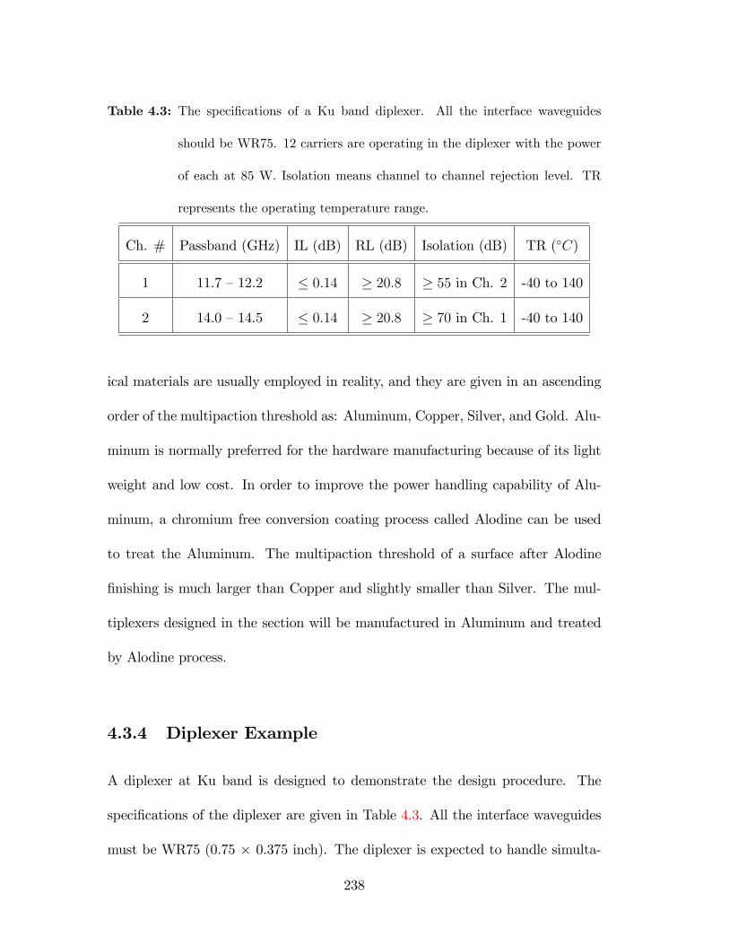
Table 4.3: The speci�cations of a Ku band diplexer. All the interface waveguides
should be WR75. 12 carriers are operating in the diplexer with the power
of each at 85 W. Isolation means channel to channel rejection level. TR
represents the operating temperature range.
Ch. # Passband (GHz) IL (dB) RL (dB) Isolation (dB) TR (�C)
1 11.7 �12.2 � 0:14 � 20:8 � 55 in Ch. 2 -40 to 140
2 14.0 �14.5 � 0:14 � 20:8 � 70 in Ch. 1 -40 to 140
ical materials are usually employed in reality, and they are given in an ascending
order of the multipaction threshold as: Aluminum, Copper, Silver, and Gold. Alu-
minum is normally preferred for the hardware manufacturing because of its light
weight and low cost. In order to improve the power handling capability of Alu-
minum, a chromium free conversion coating process called Alodine can be used
to treat the Aluminum. The multipaction threshold of a surface after Alodine
�nishing is much larger than Copper and slightly smaller than Silver. The mul-
tiplexers designed in the section will be manufactured in Aluminum and treated
by Alodine process.
4.3.4 Diplexer Example
A diplexer at Ku band is designed to demonstrate the design procedure. The
speci�cations of the diplexer are given in Table 4.3. All the interface waveguides
must be WR75 (0.75 � 0.375 inch). The diplexer is expected to handle simulta-
238
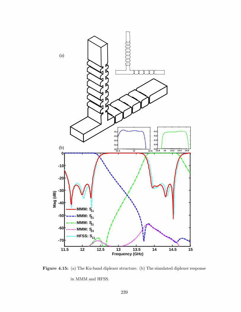
11.5 12 12.5 13 13.5 14 14.5 15
70
60
50
40
30
20
10
0
Mag
(dB
)
Frequency (GHz)
MMM: S11
MMM: S21
MMM: S31
MMM: S23
HFSS: S11
11.5 12 12.5 13 13.5 14 14.5 15
70
60
50
40
30
20
10
0
Mag
(dB
)
Frequency (GHz)
MMM: S11
MMM: S21
MMM: S31
MMM: S23
HFSS: S11
(a)
(b)11.5 12 12.5
0.5
0.4
0.3
0.2
0.1
11.5 12 12.50.5
0.4
0.3
0.2
0.1
13.8 14 14.2 14.4 14.60.5
0.4
0.3
0.2
0.1
13.8 14 14.2 14.4 14.60.5
0.4
0.3
0.2
0.1
Figure 4.15: (a) The Ku-band diplexer structure. (b) The simulated diplexer response
in MMM and HFSS.
239
neously RF power of 12 carriers with each at 85 W. In single carrier analysis, the
transmitting �lter should have a multipaction margin larger than 3 dB. In multiple
carrier analysis, 6 dB or greater margin between the 20-gap-crossing multipaction
power and the applied power levels should exist.
In order to compensate the e¤ect of the temperature drifting, the designed
�lter bandwidths are enlarged 100 MHz wider than the required bandwidths, i.e.
the channel passbands are designed to be: 11.65 �12.25 GHz and 13.95 �14.55
GHz. A 3 dB or more margin for return loss and isolation is achieved between
the designed �lters and the required ones to compensate the possible performance
degrading due to the manufacturing tolerance.
For the waveguide lowpass �lter, the height of the low-z waveguide is de-
termined according to the requirement of the multipaction margin. The height
should be selected as the lowest possible value to reduce the �lter volume. By
using the tool of multipaction calculator, the height of the low-z waveguide is de-
cided to be 0.15 inch to have a 3.36 dB multipaction margin with Alodine surface
�nishing. The height of the high-z waveguide is determined to be 0.45 inch to
achieve a 60 dB isolation in the receiving band with a 15-order lowpass �lter. A
4-order bandpass �lter is used for the receiving �lter to achieve a 73 dB isolation
in the transmitting band.
The designed �lter structure is shown in Fig. 4.15(a). The simulated re-
sponses of the diplexer in MMM and HFSS are shown in Fig. 4.15(b). A good
agreement can be noticed. This diplexer is being made of Aluminum. To estimate
the insertion loss of each channel, a HFSS simulation is performed with the con-
240
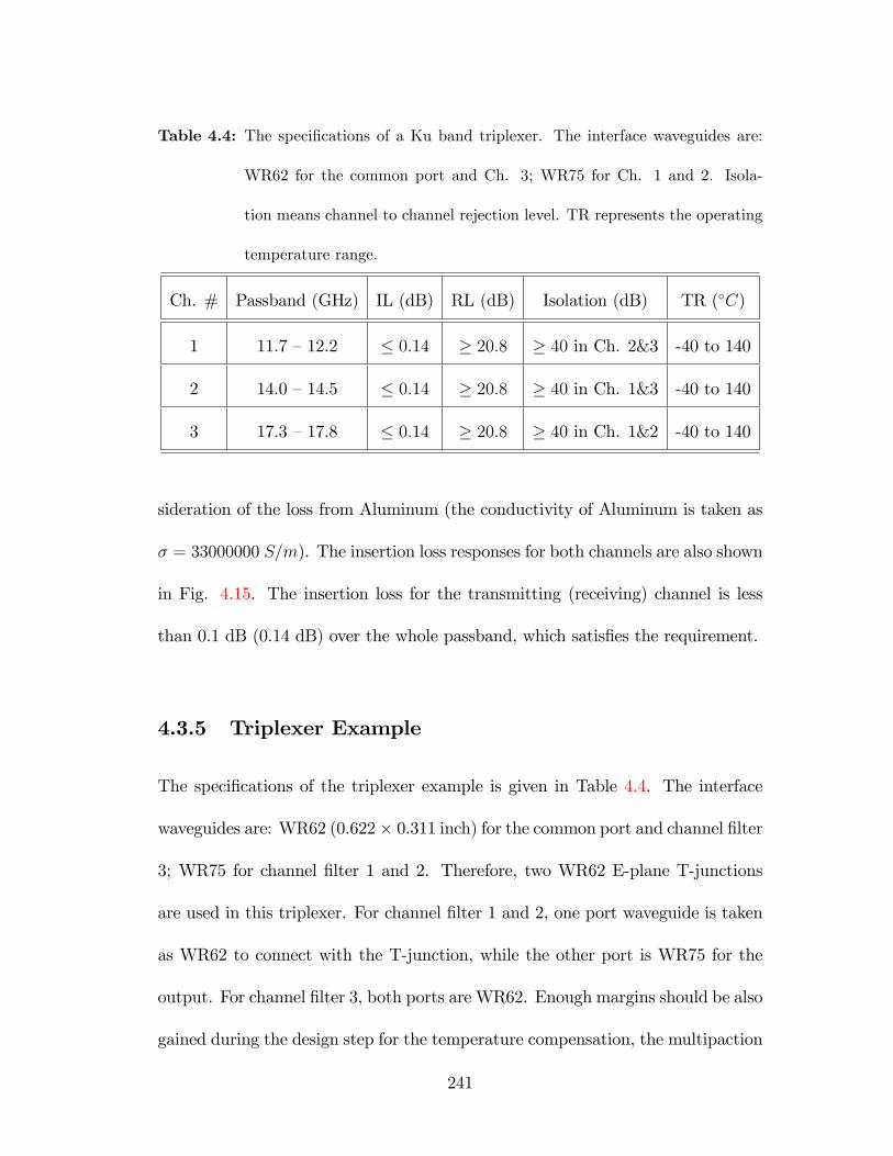
Table 4.4: The speci�cations of a Ku band triplexer. The interface waveguides are:
WR62 for the common port and Ch. 3; WR75 for Ch. 1 and 2. Isola-
tion means channel to channel rejection level. TR represents the operating
temperature range.
Ch. # Passband (GHz) IL (dB) RL (dB) Isolation (dB) TR (�C)
1 11.7 �12.2 � 0:14 � 20:8 � 40 in Ch. 2&3 -40 to 140
2 14.0 �14.5 � 0:14 � 20:8 � 40 in Ch. 1&3 -40 to 140
3 17.3 �17.8 � 0:14 � 20:8 � 40 in Ch. 1&2 -40 to 140
sideration of the loss from Aluminum (the conductivity of Aluminum is taken as
� = 33000000 S=m). The insertion loss responses for both channels are also shown
in Fig. 4.15. The insertion loss for the transmitting (receiving) channel is less
than 0.1 dB (0.14 dB) over the whole passband, which satis�es the requirement.
4.3.5 Triplexer Example
The speci�cations of the triplexer example is given in Table 4.4. The interface
waveguides are: WR62 (0.622� 0.311 inch) for the common port and channel �lter
3; WR75 for channel �lter 1 and 2. Therefore, two WR62 E-plane T-junctions
are used in this triplexer. For channel �lter 1 and 2, one port waveguide is taken
as WR62 to connect with the T-junction, while the other port is WR75 for the
output. For channel �lter 3, both ports are WR62. Enough margins should be also
gained during the design step for the temperature compensation, the multipaction
241
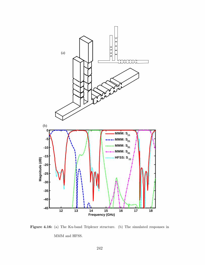
12 13 14 15 16 17 1845
40
35
30
25
20
15
10
5
0
Mag
nitu
de (d
B)
Frequency (GHz)
MMM: S11
MMM: S21
MMM: S31
MMM: S41
HFSS: S 11
12 13 14 15 16 17 1845
40
35
30
25
20
15
10
5
0
Mag
nitu
de (d
B)
Frequency (GHz)
MMM: S11
MMM: S21
MMM: S31
MMM: S41
HFSS: S 11
(a)
(b)
Figure 4.16: (a) The Ku-band Triplexer structure. (b) The simulated responses in
MMM and HFSS.
242
margin, the return losses, and the channel to channel isolations.
The channel �lter 1 and 2 can be designed with the same waveguide for
both ports �rst. One port is then replaced by the required interface waveguide,
which usually degrades the �lter performance. Optimization can be applied again
to achieve the desired �lter requirements. The designed triplexer structure and
simulated responses are shown in Fig. 4.16(a) and (b), respectively. A good
agreement can be seen between the responses from MMM and HFSS.
4.4 LTCCMultiplexers Using Stripline Junctions
4.4.1 Introduction
With the development of the LTCC technology, it is desirable to integrate all the
components of a microwave system into one single circuit board. The microwave
passive components, e.g. �lters and multiplexers, are usually placed underneath
other active components due to their bulk size. Stripline structures are the most
common choices for microwave passive components in a circuit board because of
their practical features, namely compact size, wide applicable frequency range,
easy processing in LTCC, and convenient connection with active elements [220].
A major drawback of stripline structures is the high loss, which is very critical for
�lters and multiplexers. Nevertheless, stripline and waveguide structures can be
combined together for the realizations of �lters and multiplexers to improve the
insertion loss, e.g. ridge waveguide coupled stripline resonator �lters presented in
243
Sec. 3.4 (p. 132).
In this section, novel multiplexer/diplexer con�gurations using stripline junc-
tions are presented. They are applicable to LTCC applications and can be inte-
grated easily with other components. A good insertion loss performance is also
able to be achieved. Such multiplexers can be rigorously designed in MMM, which
guarantees their performance after the manufacturing in LTCC (In practice, it is
no possible to tune a LTCC component.). A diplexer example is designed in this
section to show the validity of the concept.
4.4.2 Multiplexer Con�guration
Two types of stripline junctions can be employed for the multiplexer structure:
stripline bifurcation junction and stripline manifold junction as shown in Fig.
4.17(a) and (b), respectively. Stripline bifurcation junction is appropriate for a
diplexer design with relatively broad bandwidth (> 30%) and high integration
requirement, while stripline manifold junction is a good choice for multiplexer
designs with relatively narrow bandwidths (< 20%). A transformer is usually
required in the bifurcation junction to improve the matching. These two junctions
can be modeled by MMM with the theories of GSM and GAM, respectively [35].
Ridge waveguide coupled stripline resonator �lters are used for the channel
�lters in a multiplexer to gain a good insertion loss performance. Shown in Fig.
4.17(c) is a typical �lter structure. Compared with the �lter structure in Fig.
3.37(a) (p. 135), the external couplings of the �lter in Fig. 4.17(c) are provided
244
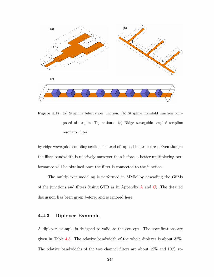
(a) (b)
(c)
Figure 4.17: (a) Stripline bifurcation junction. (b) Stripline manifold junction com-
posed of stripline T-junctions. (c) Ridge waveguide coupled stripline
resonator �lter.
by ridge waveguide coupling sections instead of tapped-in structures. Even though
the �lter bandwidth is relatively narrower than before, a better multiplexing per-
formance will be obtained once the �lter is connected to the junction.
The multiplexer modeling is performed in MMM by cascading the GSMs
of the junctions and �lters (using GTR as in Appendix A and C). The detailed
discussion has been given before, and is ignored here.
4.4.3 Diplexer Example
A diplexer example is designed to validate the concept. The speci�cations are
given in Table 4.5. The relative bandwidth of the whole diplexer is about 32%.
The relative bandwidths of the two channel �lters are about 12% and 10%, re-
245
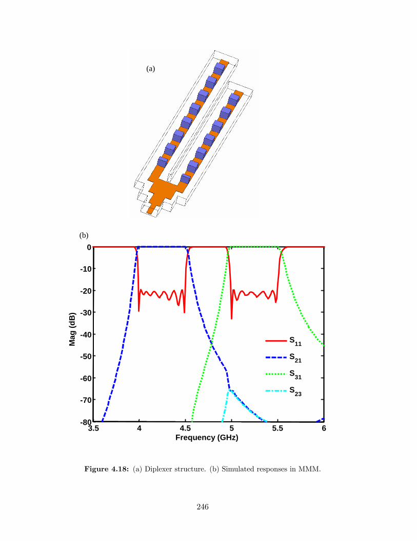
3.5 4 4.5 5 5.5 680
70
60
50
40
30
20
10
0
Mag
(dB
)
Frequency (GHz)
S11
S21
S31
S23
3.5 4 4.5 5 5.5 680
70
60
50
40
30
20
10
0
Mag
(dB
)
Frequency (GHz)
S11
S21
S31
S23
(a)
(b)
Figure 4.18: (a) Diplexer structure. (b) Simulated responses in MMM.
246
Table 4.5: The speci�cations of a diplexer using stripline bifurcation junction in LTCC
technology.
Channel Passband (GHz) Return Loss (dB) Isolation (dB)
1 4 �4.5 � 20 � 50 in Ch. 2
2 5 �5.5 � 20 � 50 in Ch. 1
spectively. This diplexer is expected to be realized in LTCC technology. The
LTCC parameters are: relative permittivity of ceramic "r = 5:9, thickness of
metallization ts = 0:4mil, and thickness of each ceramic layer tc = 3:74mil.
The designed diplexer structure is shown in Fig. 4.18(a). A stripline bifur-
cation junction is employed. The two channel �lters are implemented as seven-
and six-order bandpass �lters, respectively. The simulated response by MMM of
the designed diplexer is shown in Fig. 4.18(b), which satis�es all the requirements.
4.5 Wideband Diplexer Using E-plane Bifurca-
tion Junction
4.5.1 Design Task and Diplexer Con�guration
One wideband diplexer, in which one channel �lter is in K band and the other one
is in Ka band, is desired to be designed and manufactured in metallic waveguide
structures. A compact con�guration that is suitable for quasi-planar printed cir-
247
Table 4.6: The speci�cations of a wideband diplexer using E-plane bifurcation junc-
tion.
Channel Passband (GHz) Return Loss (dB) Isolation (dB)
1 19 �23 � 18 � 50 in Ch. 2
2 29.5 �31 � 18 � 50 in Ch. 1
cuit technology is required for this diplexer. The detailed speci�cations are given
in Table 4.6. The relative bandwidth of the whole diplexer is about 50%. The
two channel �lters have relative bandwidths of about 20% and 7%, respectively.
A standard waveguide WR34 (0.34 � 0.17 inch) must be used for all three ports
of the diplexer.
A waveguide junction structure must be selected �rst to satisfy two condi-
tions: wideband common-port matching and compact size suitable for integration.
An E-plane bifurcation junction as shown in Fig. 4.19(a) is an appropriate choice.
The advantages of such a junction include [3]: i) a very good matching can be
achieved over a wide frequency band. ii) It is compact, low-cost, and can be
used in quasi-planar printed components. iii) It is appropriate for E-plane split-
block housing fabrication. iv) the transformer is less complicate and easier to
design than H-plane junctions owing that the waveguide division plane is an elec-
tric wall for the fundamental mode. The designed junction response is shown in
Fig. 4.19(b), which demonstrates a power divider performance and a very good
matching at the common port over the whole operating frequency band.
248
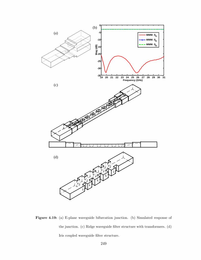
19 20 21 22 23 24 25 26 27 28 29 30 3135
30
25
20
15
10
5
0
Mag
(dB
)
Frequency (GHz)
MMM: S11
MMM: S21
MMM: S31
19 20 21 22 23 24 25 26 27 28 29 30 3135
30
25
20
15
10
5
0
Mag
(dB
)
Frequency (GHz)
MMM: S11
MMM: S21
MMM: S31
(a)(b)
(c)
(d)
Figure 4.19: (a) E-plane waveguide bifurcation junction. (b) Simulated response of
the junction. (c) Ridge waveguide �lter structure with transformers. (d)
Iris coupled waveguide �lter structure.
249
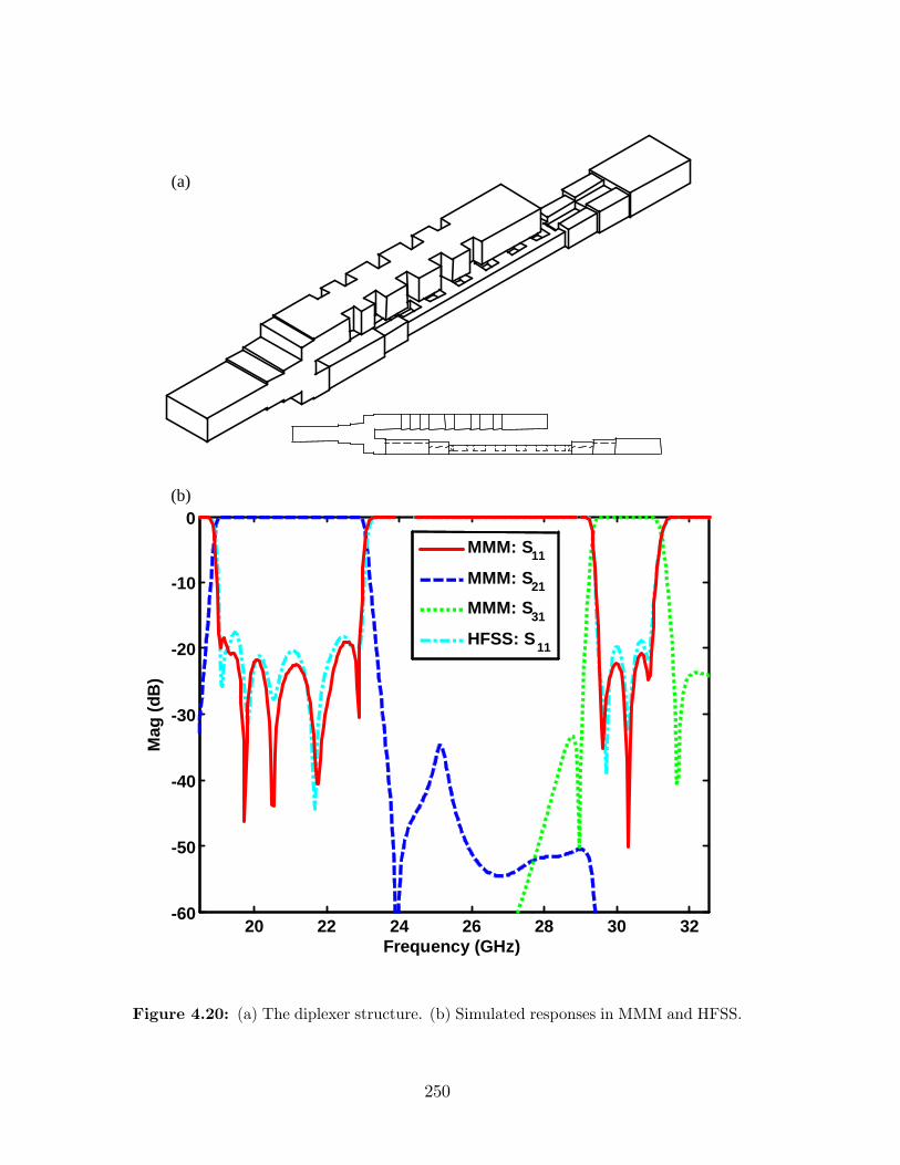
20 22 24 26 28 30 3260
50
40
30
20
10
0
Mag
(dB
)
Frequency (GHz)
MMM: S11
MMM: S21
MMM: S31
HFSS: S11
20 22 24 26 28 30 3260
50
40
30
20
10
0
Mag
(dB
)
Frequency (GHz)
MMM: S11
MMM: S21
MMM: S31
HFSS: S11
(a)
(b)
Figure 4.20: (a) The diplexer structure. (b) Simulated responses in MMM and HFSS.
250

A large separation exists between the passbands of the two channel �lters.
The stopband spurious response of channel �lter 1 must be clean (>50 dB re-
jection) inside the passband of channel �lter 2. If a bandpass �lter is used for
channel �lter 1, the higher order harmonic resonant modes must be outside the
passband of the channel �lter 2, otherwise, a stop notch will be generated in chan-
nel �lter 2. In order to have a broad bandwidth along with acceptable spurious
performance, a ridge waveguide evanescent-mode bandpass �lter as shown in Fig.
4.19(c) is employed to implement channel �lter 1 because available rectangular
waveguide �lters are unlikely to achieve the requirements. Two transformers from
ridge waveguide to rectangular waveguide are also included in the �lter structure
for the sake of connection with the above junction. An iris coupled rectangular
waveguide �lter as shown in Fig. 4.19(d) is applied to realize channel �lter 2.
4.5.2 Results
MMM is used to analyze and optimize each element and the whole diplexer. The
formulations for E-plane bifurcation junction and waveguide step discontinuities
can be found in [3, 10]. Actually, the E-plane bifurcation junction can be char-
acterized as a generalized two-port network to simplify the analysis (see [35], p.
37). The ridge waveguide �lter can be modeled by using the GTR technique as
discussed in Appendix A and C. The designed diplexer structure is shown in Fig.
4.20(a). The simulated diplexer responses in MMM and HFSS are shown in Fig.
4.20(b), from which a good agreement can be noticed.
251
Chapter 5
Conclusions and Future Research
5.1 Conclusions
This dissertation has been devoted to the development of innovated �lter and
multiplexer structures, the modeling and design of microwave components using
numerical methods, the miniaturized realization of �lters and multiplexers, and
the systematic tuning of quasi-elliptic �lters. The motivation is to develop the
optimum designs of microwave �lters and multiplexers to meet the continuously
more demanding speci�cations. Several works have been presented in this disser-
tation and proved to be successful to address the purpose.
Modern communication systems have created the need of multiple-band
quasi-elliptic �lters. An iteration procedure has been derived in Chapter 2 to
obtain the polynomial expressions of the optimum multiple-band quasi-elliptic
transfer function (i.e. the approximation procedure), from which di¤erent net-
work topologies can be synthesized through the well-known synthesis methods.
252

The approximation procedure is generalized and e¤ective for any number of pass-
bands and stopbands in a multiple-band �lter function. A powerful building-block
technique has also been presented in Chapter 2 in order to synthesize versatile
topologies. The e¤ectiveness and powerfulness of the technique are evidenced by
the given examples.
The generalized design methodologies of microwave �lters and multiplexers
have been discussed in Chapter 3 and 4. The modeling and design procedure can
be applied to any structure, regardless of the geometry of the problems. Several
novel �lter and multiplexer designs have been presented to achieve the miniatur-
ization and wideband performance, namely double- and multiple-layer coupled
resonator �lters, ridge waveguide coupled stripline resonator �lters and multi-
plexers, and ridge waveguide divider-type multiplexers. Some other �lters and
multiplexers have been developed for high power applications, which are dual-
mode �lters in circular and rectangular waveguides ,and waveguide multiplexers
using bifurcation, T- and manifold junctions. A systematic tuning procedure has
also been created for the development of quasi-elliptic �lters. The feasibility has
been validated by a dielectric resonator �lter example.
5.2 Future Research
This dissertation has concentrated on the modeling and design of microwave and
millimeter-wave �lters and multiplexers. More future research works are interested
by the author:
253

� Rigorous CAD of single- and multiple-band quasi-elliptic �lters, especially
the asymmetric �lters, in waveguide and planar structures.
� Harmonic multiple-band �lter designs with multiple-layer coupled resonator
structures.
� Spurious performance improvement by using the SIR technology in ridge
waveguide and rectangular waveguide �lters.
� Computer aided tuning of single- and multiple-band quasi-elliptic �lters in
coaxial TEM cavity and dielectric resonator technologies.
� Tunable �lters in coaxial TEM cavity and dielectric resonator technologies.
� Multiple-mode �lter designs in waveguide and dielectric resonator technolo-
gies.
� Multiport network synthesis and its application in diplexer and multiplexer
designs.
� Miniaturization of waveguide �lters and multiplexers in LTCC technology
to achieve high quality.
254
Appendix A
Generalized Transverse
Resonance (GTR) Technique1
A.1 Introduction
In this dissertation, many non-canonical waveguide geometries have been em-
ployed to design �lters and multiplexers in mode matching method (MMM). Some
of the waveguide cross-sections are shown in Fig. 1.4 (p. 13). One necessary step
in MMM is to solve the eigenmodes and eigen�elds of waveguide cross-sections.
The modes of canonical waveguides, namely rectangular, circular, coaxial circular,
and elliptical, can be obtained by analytical method [10, 12]. However, the modes
of non-canonical waveguides need to be solved by approximated numerical meth-
ods. In this dissertation, the generalized transverse resonance (GTR) technique
1The formulations in this appendix have been detailedly presented in the Ph.D. thesis of Dr.
J. A. Ruiz-Cruz [35]. They are repeated here just for completeness.
255
is used to acquire the modes of the used non-canonical waveguides.
The GTR is a well-known technique used to analyze waveguide cross-sections
that can be segmented into rectangular coordinates. The literature in GTR is
very extensive, and its theory and applications can be found in many references
[14, 35, 45, 46, 49�51]. The complete GTR formulations for TEM, TE and TM
modes have been detailedly presented in [35]. Nevertheless, the formulations are
repeated again in this appendix since some new structures in this dissertations
are analyzed by the GTR.
A.2 Problem Statement
It is well-known that the electromagnetic �eld in homogeneous waveguide can
be described in terms of TEM, TE and TM modes. The theory of waveguides
is well established and reported in many textbooks [7, 13]. The properties of
TEM, TE and TM modes are summarized in Table A.1. The �eld of a TEM,
TE or TM mode can be derived from a scalar potential � that is the solution of
Laplace or Helmholtz equation with appropriate boundary conditions. Therefore,
the objective is to �nd the cuto¤ wavenumber kc of the modes and the associated
scalar potential �. Once � is solved, the components of the eigen�eld can be
easily obtained by using the basic gradient operations in Table A.1.
In order to solve the eigenmodes and eigen�elds of the non-canonical waveguides
2For a waveguide with P + 1 conductors (each one with contour Cp), P TEM modes exist.
The boundary conditions are �m = �m;p on Cp, p = 1; 2; :::; P . �m;p is a constant potential.
256
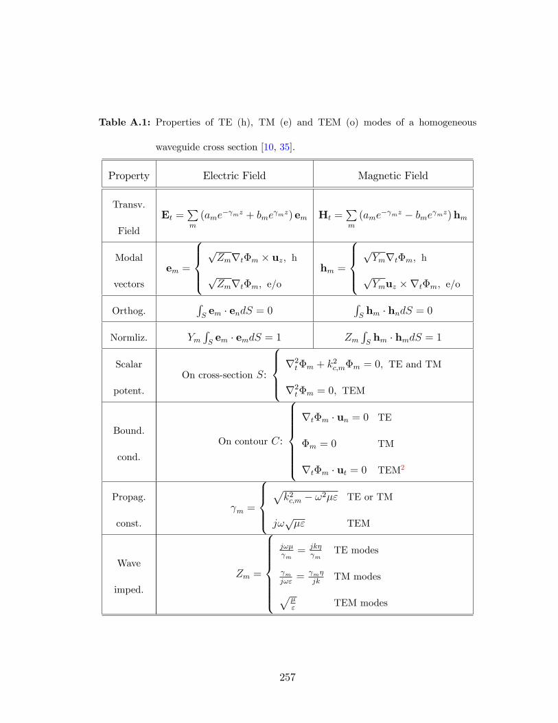
Table A.1: Properties of TE (h), TM (e) and TEM (o) modes of a homogeneous
waveguide cross section [10, 35].
Property Electric Field Magnetic Field
Transv.
Field
Et =Pm
(ame� mz + bme
mz) em Ht =Pm
(ame� mz � bme mz)hm
Modal
vectors
em =
8>><>>:pZmrt�m � uz; hpZmrt�m; e/o
hm =
8>><>>:pYmrt�m; hpYmuz �rt�m; e/o
Orthog.RSem � endS = 0
RShm � hndS = 0
Normliz. YmRSem � emdS = 1 Zm
RShm � hmdS = 1
Scalar
potent.
On cross-section S:
8>><>>:r2t�m + k2c;m�m = 0; TE and TM
r2t�m = 0; TEM
Bound.
cond.
On contour C:
8>>>>>><>>>>>>:rt�m � un = 0 TE
�m = 0 TM
rt�m � ut = 0 TEM2
Propag.
const.
m =
8>><>>:pk2c;m � !2�" TE or TM
j!p�" TEM
Wave
imped.
Zm =
8>>>>>><>>>>>>:
j!� m= jk�
mTE modes
mj!"= m�
jkTM modesp
�"
TEM modes
257
as shown in Fig. 1.4, a generic waveguide cross-section as shown in Fig. A.1(a)
is considered. The generic structure consists of a cascade of M parallel-plate
regions along the x-direction. Rectangular conductors, which create subregions
in one region, may exist in some of the parallel-plate regions, e.g. region m in
Fig. A.1(a). Each top and bottom wall may have di¤erent boundary conditions,
namely PEW or PMW, according to the symmetry of the geometries. This generic
cross-section is a generalized waveguide, and all the non-canonical waveguides in
this dissertation are special cases of it.
The GTR is used to characterize the generic waveguide cross-section in
A.1(a). Basically, the generic structure can be represented as a generalized trans-
verse network as shown in Fig. A.1(b). Each parallel-plate region is considered as
multiple-electric-port transmission lines. The discontinuity (Dm in Fig. A.1(b))
between two parallel-plate regions is characterized by GSM. The two terminal
ends are either short or open circuit depending on the symmetry of the structure.
Therefore, the generalized transverse network in Fig. A.1(b) is actually a resonant
network, and its resonant condition will provide the cuto¤wavenumber kc of each
eigenmode of the waveguide structure.
Therefore, the problem can be stated as: Given a non-canonical waveguide
that can be segmented into many parallel-plate regions, a generalized transverse
resonance network needs to be created to represent the structure, and the natural
resonant condition is used to solve the eigenmodes and eigen�elds of the waveguide.
The detailed formulations for characterizing the discontinuities and creating the
resonance network are given next.
258
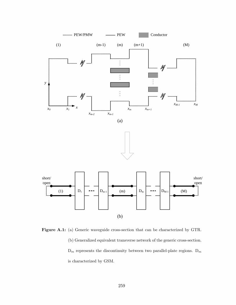
PEW/PMW PEW Conductor
(1) (m1) (m) (m+1) (M)
x0 x1xm2 xm1
xm xm+1
xM1 xMx
y
D1 Dm1 Dm DM1(1) (m) (M)
(a)
(b)
short/open
short/open
Figure A.1: (a) Generic waveguide cross-section that can be characterized by GTR.
(b) Generalized equivalent transverse network of the generic cross-section.
Dm represents the discontinuity between two parallel-plate regions. Dm
is characterized by GSM.
259
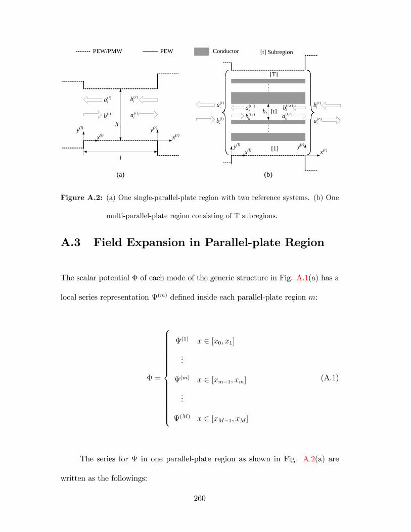
y(l)
x(l)y(r)
x(r)
l
h
( )lia
( )lib
( )rib
( )ria
y(l)
x(l)y(r)
x(r)
( )lia
( )lib
( )rib
( )ria
[1]
ht
( , )t lka( , )t lkb
( , )t rkb( , )t rka
[t]
[T]
PEW/PMW PEW Conductor [t] Subregion
(a) (b)
Figure A.2: (a) One single-parallel-plate region with two reference systems. (b) One
multi-parallel-plate region consisting of T subregions.
A.3 Field Expansion in Parallel-plate Region
The scalar potential � of each mode of the generic structure in Fig. A.1(a) has a
local series representation (m) de�ned inside each parallel-plate region m:
� =
8>>>>>>>>>>>>>><>>>>>>>>>>>>>>:
(1) x 2 [x0; x1]...
(m) x 2 [xm�1; xm]...
(M) x 2 [xM�1; xM ]
(A.1)
The series for in one parallel-plate region as shown in Fig. A.2(a) are
written as the followings:
260
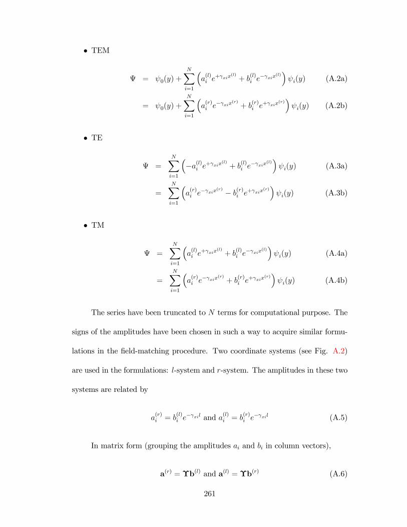
� TEM
= 0(y) +NXi=1
�a(l)i e
+ xix(l)
+ b(l)i e
� xix(l)� i(y) (A.2a)
= 0(y) +
NXi=1
�a(r)i e� xix
(r)
+ b(r)i e+ xix
(r)� i(y) (A.2b)
� TE
=NXi=1
��a(l)i e+ xix
(l)
+ b(l)i e
� xix(l)� i(y) (A.3a)
=NXi=1
�a(r)i e� xix
(r) � b(r)i e+ xix(r)� i(y) (A.3b)
� TM
=NXi=1
�a(l)i e
+ xix(l)
+ b(l)i e
� xix(l)� i(y) (A.4a)
=NXi=1
�a(r)i e� xix
(r)
+ b(r)i e+ xix
(r)� i(y) (A.4b)
The series have been truncated to N terms for computational purpose. The
signs of the amplitudes have been chosen in such a way to acquire similar formu-
lations in the �eld-matching procedure. Two coordinate systems (see Fig. A.2)
are used in the formulations: l-system and r-system. The amplitudes in these two
systems are related by
a(r)i = b
(l)i e
� xil and a(l)i = b(r)i e� xil (A.5)
In matrix form (grouping the amplitudes ai and bi in column vectors),
a(r) = �b(l) and a(l) = �b(r) (A.6)
261
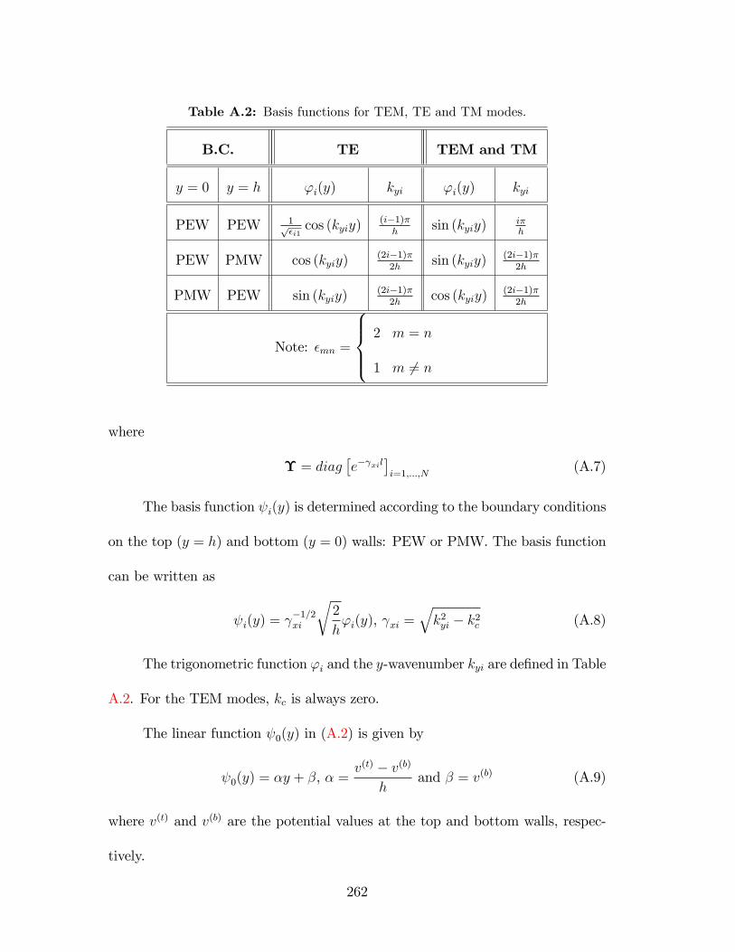
Table A.2: Basis functions for TEM, TE and TM modes.
B.C. TE TEM and TM
y = 0 y = h 'i(y) kyi 'i(y) kyi
PEW PEW 1p�i1cos (kyiy)
(i�1)�h
sin (kyiy)i�h
PEW PMW cos (kyiy)(2i�1)�2h
sin (kyiy)(2i�1)�2h
PMW PEW sin (kyiy)(2i�1)�2h
cos (kyiy)(2i�1)�2h
Note: �mn =
8>><>>:2 m = n
1 m 6= n
where
� = diag�e� xil
�i=1;:::;N
(A.7)
The basis function i(y) is determined according to the boundary conditions
on the top (y = h) and bottom (y = 0) walls: PEW or PMW. The basis function
can be written as
i(y) = �1=2xi
r2
h'i(y), xi =
qk2yi � k2c (A.8)
The trigonometric function 'i and the y-wavenumber kyi are de�ned in Table
A.2. For the TEM modes, kc is always zero.
The linear function 0(y) in (A.2) is given by
0(y) = �y + �, � =v(t) � v(b)
hand � = v(b) (A.9)
where v(t) and v(b) are the potential values at the top and bottom walls, respec-
tively.
262
The term multi-parallel-plate region is used to refer one parallel-plate re-
gion having multiple conductors inside (see region m in Fig. A.1(a)). In a multi-
parallel-plate region as shown in Fig. A.2(b), there are T parallel-plate subregions.
In each subregion t, the function can be expanded in a series formally identical
to (A.2), (A.3), and (A.4) for TEM, TE, and TM modes, respectively. The am-
plitudes of each subregion can be grouped together as one set of amplitudes for
the multi-parallel-plate region:
a(l) =�a(1;l); � � � ; a(t;l); � � � a(T;l)
�t, a(t;l) =
ha(t;l)1 ; � � � ; a(t;l)Nt
itb(l) =
�b(1;l); � � � ;b(t;l); � � �b(T;l)
�t, b(t;l) =
hb(t;l)1 ; � � � ; b(t;l)Nt
ita(r) =
�a(1;r); � � � ; a(t;r); � � � a(T;r)
�t, a(t;r) =
ha(t;r)1 ; � � � ; a(t;r)Nt
itb(r) =
�b(1;r); � � � ;b(t;r); � � �b(T;r)
�t, b(t;r) =
hb(t;r)1 ; � � � ; b(t;r)Nt
it(A.10)
where Nt is the truncated number of terms for each subregion. The amplitudes
in the two coordinate systems are related by (A.6), where the matrix � is now
constructed by the subregions
� = diag��(t)
�t=1;:::;T
, �(t) = diaghe�
(t)xi lii=1;:::;Nt
(A.11)
Therefore, a multi-parallel-plate region can be considered to be a general-
ized parallel-plate region, whose mathematical operations are similar to a single
parallel-plate region.
263
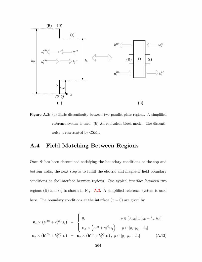
( )Bib
( )Bia
( )sia
( )sib
x
y
(0, 0)
hB hs
y0
D
(B)
(s)
(B) (s)
( )Bib
( )Bia
( )sia
( )sib
(D)
(a) (b)
Figure A.3: (a) Basic discontinuity between two parallel-plate regions. A simpli�ed
reference system is used. (b) An equivalent block model. The disconti-
nuity is represented by GSMx.
A.4 Field Matching Between Regions
Once has been determined satisfying the boundary conditions at the top and
bottom walls, the next step is to ful�ll the electric and magnetic �eld boundary
conditions at the interface between regions. One typical interface between two
regions (B) and (s) is shown in Fig. A.3. A simpli�ed reference system is used
here. The boundary conditions at the interface (x = 0) are given by
ux ��e(B) + e(B)z uz
�=
8>><>>:0; y 2 [0; y0] [ [y0 + hs; hB]
ux ��e(s) + e
(s)z uz
�; y 2 [y0; y0 + hs]
ux ��h(B) + h(B)z uz
�= ux �
�h(s) + h(s)z uz
�; y 2 [y0; y0 + hs] (A.12)
264
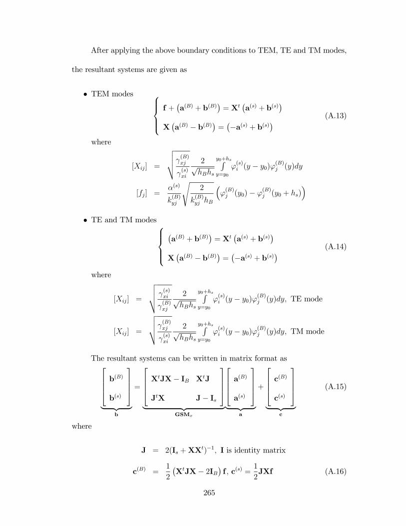
After applying the above boundary conditions to TEM, TE and TM modes,
the resultant systems are given as
� TEM modes 8>><>>:f +
�a(B) + b(B)
�= Xt
�a(s) + b(s)
�X�a(B) � b(B)
�=��a(s) + b(s)
� (A.13)
where
[Xij] =
vuut (B)xj
(s)xi
2phBhs
y0+hsRy=y0
'(s)i (y � y0)'
(B)j (y)dy
[fj] =�(s)
k(B)yj
s2
k(B)yj hB
�'(B)j (y0)� '(B)j (y0 + hs)
�� TE and TM modes8>><>>:
�a(B) + b(B)
�= Xt
�a(s) + b(s)
�X�a(B) � b(B)
�=��a(s) + b(s)
� (A.14)
where
[Xij] =
vuut (s)xi
(B)xj
2phBhs
y0+hsRy=y0
'(s)i (y � y0)'
(B)j (y)dy; TE mode
[Xij] =
vuut (B)xj
(s)xi
2phBhs
y0+hsRy=y0
'(s)i (y � y0)'
(B)j (y)dy; TM mode
The resultant systems can be written in matrix format as2664 b(B)b(s)
3775| {z }
b
=
2664 XtJX� IB XtJ
JtX J� Is
3775| {z }
GSMx
2664 a(B)a(s)
3775| {z }
a
+
2664 c(B)c(s)
3775| {z }
c
(A.15)
where
J = 2(Is +XXt)�1; I is identity matrix
c(B) =1
2
�XtJX� 2IB
�f ; c(s) =
1
2JXf (A.16)
265
Therefore, each interface can be characterized by GSMx for TE and TM
modes (c is null). For TEM modes, a vector c is generated. The GSMx and c
for a interface between multi-parallel-plate regions can be obtained similarly as
the above procedure. The only di¤erence is that the matrix X and vector f are
composed of blocks from each subregion.
A.5 Characteristic System
With the matrix characterization of every basic discontinuity in Fig. A.3(b), the
complete matrix representation of the problem as shown in Fig. A.1(b) can be
obtained by means of cascading of the characterizations of each discontinuity. The
GSMx (S(T )) that relates the amplitudes at x = x0 and x = xM can be easily
computed to obtain the total characterization of the structure:2664 b(T )1
b(T )2
3775| {z }
b(T )
=
2664 S(T )11 S
(T )12
S(T )21 S
(T )22
3775| {z }
S(T )
2664 a(T )1
a(T )2
3775| {z }
a(T )
+
2664 c(T )1
c(T )2
3775| {z }
c(T )
(A.17)
where 8>><>>:b(T )1 = a(1;l) b
(T )2 = a(M;r)
a(T )1 = b(1;l) a
(T )2 = b(M;r)
(A.18)
In order to obtain the characteristic equation for the whole system (see Fig.
A.1), the conditions at the lateral walls (PEW or PMW) are applied:2664 b(1;l)b(M;r)
3775 =2664 �L 0
0 �R
3775| {z }
�
2664 a(1;l)a(M;r)
3775 ; �L;�R =8>><>>:�I; PEW
+I; PMW
(A.19)
266
The characteristic system is therefore represented by
���1 � S(T )
�a(T ) = c(T ) (A.20)
For TEM modes, the solution of this characteristic system provides the
amplitudes at the lateral walls, while for TE and TM modes, a mode can exist
only if
det���1 � S(T )
�= det
���1 � S(T )(kc)
�= 0
The real roots of the above characteristic equation are the cuto¤wavenumber
kc of the modes. These roots can be solved by Muller method [114] for real
argument functions. Once kc is known for each mode, the amplitudes in each
region can be obtained by an iterative procedure of de-cascading.
267
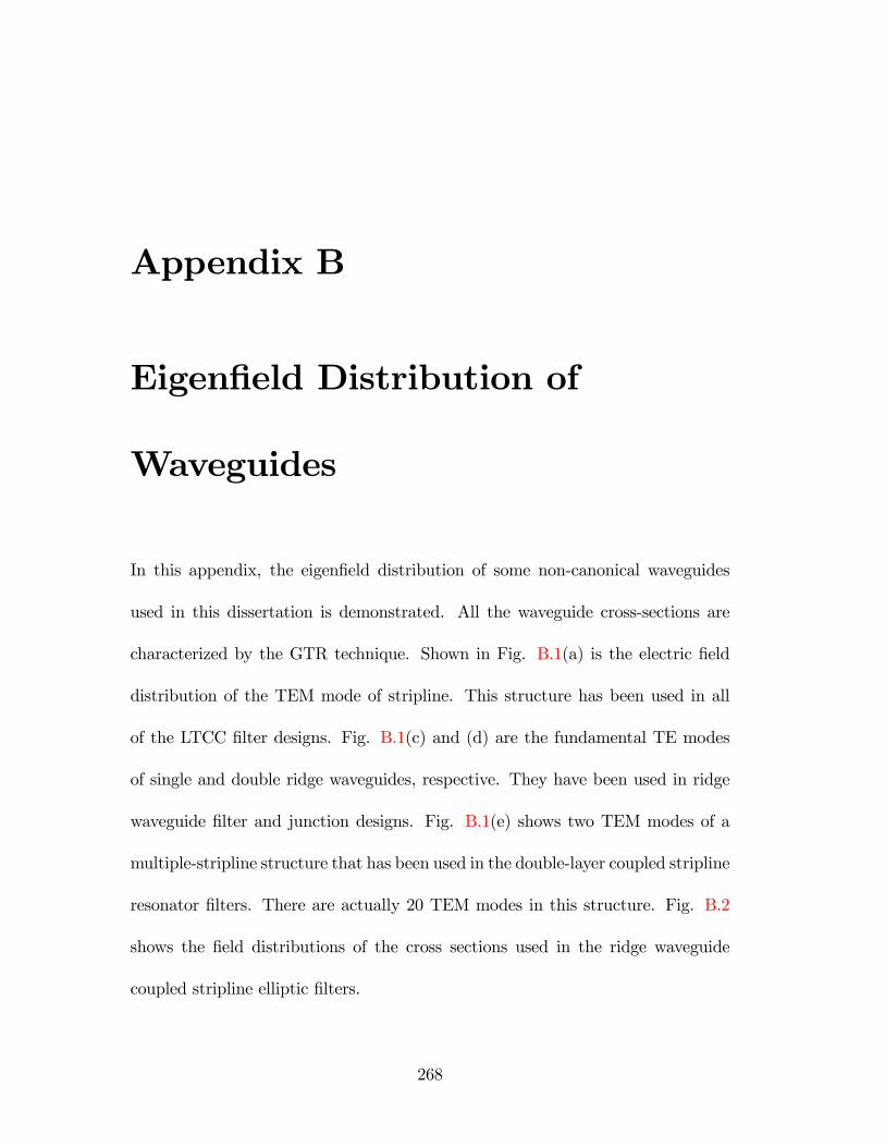
Appendix B
Eigen�eld Distribution of
Waveguides
In this appendix, the eigen�eld distribution of some non-canonical waveguides
used in this dissertation is demonstrated. All the waveguide cross-sections are
characterized by the GTR technique. Shown in Fig. B.1(a) is the electric �eld
distribution of the TEM mode of stripline. This structure has been used in all
of the LTCC �lter designs. Fig. B.1(c) and (d) are the fundamental TE modes
of single and double ridge waveguides, respective. They have been used in ridge
waveguide �lter and junction designs. Fig. B.1(e) shows two TEM modes of a
multiple-stripline structure that has been used in the double-layer coupled stripline
resonator �lters. There are actually 20 TEM modes in this structure. Fig. B.2
shows the �eld distributions of the cross sections used in the ridge waveguide
coupled stripline elliptic �lters.
268
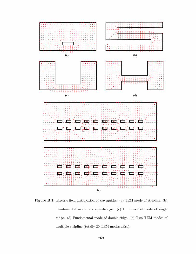
(a) (b)
(c) (d)
(e)
Figure B.1: Electric �eld distribution of waveguides. (a) TEM mode of stripline. (b)
Fundamental mode of coupled-ridge. (c) Fundamental mode of single
ridge. (d) Fundamental mode of double ridge. (e) Two TEM modes of
multiple-stripline (totally 20 TEM modes exist).
269
PMWPMW PEWPEW
PMWPMW PEWPEW
PMWPMW PEWPEW
(a) (b)
(c) (d)
(e) (f)
Figure B.2: Electric �eld distribution of waveguides. (a) TEM mode with PMW of
coupled stripline. (b) TEM mode with PEW of coupled stripline. (c)
TEM mode with PMW of ridge-stripline. (d) TEM mode with PEW of
ridge-stripline. (e) The �rst TE mode with PMW of ridge-stripline. (f)
The �rst TE mode with PEW of ridge-stripline.
270
Appendix C
Coupling Integrals between
Waveguides1
In the application of the mode matching technique between waveguides (one large
and one small in the most general case), it is usually necessary to calculate the
coupling integrals between the modes of the waveguides (e.g. matrix X in Table
1.2, p. 16). Two types of inner products need to be computed if the scalar
potential � is used to evaluate the coupling integral, which are
X1 =
ZZS
rt�1 � rt�2dS; X2 =
ZZS
rt�1 � rt�2 � uzdS (C.1)
where �1 and �2 are two modes belonging to two di¤erent waveguides. The
surface S usually coincides with the area of the small waveguide cross-section. It
is worth noting that the coupling integral between a TEM/TM mode of the small
waveguide with a TE mode of the large waveguide is always equal to zero.1The formulations in this appendix have been presented in the Ph.D. thesis of Dr. J. A.
Ruiz-Cruz [35] before.
271
In this appendix, the coupling integral between two waveguides character-
ized by GTR (see p. 255) is formularized. The surface S of the discontinuity
between two GTR waveguides can be decomposed into non-intersecting rectangu-
lar domains Rk as
S = [kRk (C.2)
and then the inner product is given by
X1 =Xk
X1;Ri ; X2 =Xk
X2;Rk
where X1;Rk and X2;Rk are the local inner products evaluated over domain Rk.
In each domain R (index k is ignored), the local representation of the
scalar potential � of the modes can be written as
=NXi=1
�Apie
+ ix + Anie� ix
�fi (y) + �y + const (C.3)
where the x-coordinate has been transformed to the local system of domain R
(The transformed coe¢ cients are counted into Api and Ani). Api and Ani are
also related to the amplitudes in (A.2), (A.3) and (A.4) in terms of normalization
constants and sign changes.
Assuming that the bottom (y = 0) of domain R has an o¤set y0 with respect
to the the corresponding parallel-plate region in the waveguide, the function in
y is then given as fi(y) = 'i(y + y0). For TE and TM modes, � = 0. In the
following discussions, domain R is assumed to have a width w and a height h.
The inner product X1;R and X2;R over domain R are then evaluated as
X1;R =
ZZR
rt1 � rt2dS; X2;R =
ZZR
rt1 � rt2 � uzdS (C.4)
272
The partial derivatives of (C.3) are calculated as
@
@x=
NXi=1
i�Apie
+ ix � Anie� ix�fi(y) � x
@
@y= �+
NXi=1
�Apie
+ ix + Anie� ix
�f0
i (y) � �+y (C.5)
Thus, the following equations can be written:
1x =
N1Xi=1
(1)i
�A(1)pi e
+ (1)i x � A(1)ni e�
(1)i x�f(1)i (y)
1y =
N1Xi=1
�A(1)pi e
+ (1)i x + A
(1)ni e
� (1)i x�f(1)0
i (y)
2x =
N2Xj=1
(2)j
�A(2)pj e
+ (2)j x � A(2)nj e�
(2)j x�f(2)j (y)
2y =
N2Xj=1
�A(2)pj e
+ (2)j x + A
(2)nj e
� (2)j x�f(2)0
j (y) (C.6)
Equation (C.4) can then be calculated through the following identities
rt1 � rt2 = 1x2x +1y2y + �12y + �21y + �1�2
rt1 � rt2 � uz = 1x2y �1y2x + �21x � �12x (C.7)
and
1x2x =
N1Xi=1
N2Xj=1
(1)i
(2)j
�A(1)pi e
+ (1)i x � A(1)ni e�
(1)i x���
A(2)pj e
+ (2)j x � A(2)nj e�
(2)j x�f(1)i (y)f
(2)j (y)
1y2y =
N1Xi=1
N2Xj=1
�A(1)pi e
+ (1)i x + A
(1)ni e
� (1)i x���
A(2)pj e
+ (2)j x + A
(2)nj e
� (2)j x�f(1)0
i (y)f(2)0
j (y)
1x2y =
N1Xi=1
N2Xj=1
(1)i
�A(1)pi e
+ (1)i x � A(1)ni e�
(1)i x���
A(2)pj e
+ (2)j x + A
(2)nj e
� (2)j x�f(1)i (y)f
(2)0
j (y)
273
1y2x =
N1Xi=1
N2Xj=1
(2)j
�A(1)pi e
+ (1)i x + A
(1)ni e
� (1)i x���
A(2)pj e
+ (2)j x � A(2)nj e�
(2)j x�f(1)0
i (y)f(2)j (y) (C.8)
Therefore, X1;R and X2;R can be obtained by calculating the integral of
each term in (C.7) over domain R. All the integrals are analytical since only
exponential and trigonometric functions are involved. For example,
ZZR
1x2xdS =
N1Xi=1
N2Xj=1
(1)i
(2)j �26666664
A(1)pi A
(2)pj
wZx=0
e(+ (1)i +
(2)j )xdx� A(1)pi A
(2)nj
wZx=0
e(+ (1)i � (2)j )xdx
�A(1)ni A(2)pj
wZx=0
e(� (1)i +
(2)j )xdx+ A
(1)ni A
(2)nj
wZx=0
e(� (1)i � (2)j )xdx
37777775 �hZ
y=0
f(1)i (y)f
(2)j (y)dy (C.9)
Other integral terms can be computed in similar procedures, and are not listed
here.
274

Bibliography
[1] G. L. Matthaei, L. Young, and E. M. T. Jones, Microwave Filters,Impedance-Matching Networks and Coupling Structures. Boston: ArtechHouse, 1980.
[2] D. M. Pozar, Microwave Engineering. New York: John Wiley, 1998.
[3] J. Uher, J. Bornemann, and U. Rosenberg, Waveguide Components for An-tenna Feed Systems. Boston: Artech House, 1993.
[4] M. Williamson, The Communications Satellite. Bristol and New York:Adam Hilger, 1990.
[5] D. Roddy, Satellite Communications. New York: McGraw-Hill, 2006.
[6] A. A. Oliner, �Historical perspectives on microwave �eld theory,� IEEETrans. Microw. Theory Tech., vol. 32, pp. 1022�1045, Sept. 1984.
[7] N. Marcuvitz, Waveguide Handbook. New York: McGraw-Hill, 1951.
[8] C. Montgomery, R. Dicke, and E. Purcell, Principles of Microwave Circuits.London: IEE Electromagnetic waves series 25, 1987.
[9] R. Levy and S. Cohn, �A history of microwave �lter research, design, anddevelopment,�IEEE Trans. Microw. Theory Tech., vol. 32, pp. 1055�1067,Sept. 1984.
[10] G. Conciauro, M. Guglielmi, and R. Sorrentino, Advanced modal analysis:CAD techniques for waveguide components and �lters. John Wiley, 1999.
[11] J. D. G. Swanson and W. J. R. Hoefer, Microwave Circuit Modeling UsingElectromagnetic Field Simulation. Boston, London: Artech House, 2003.
[12] P. Morse and H. Feshbach, Methods of Theoretical Physics. McGraw-Hill,1953.
[13] R. E. Collin, Field Theory of Guided Waves. New York: IEEE Press, 1991.
[14] T. Itoh (editor), Numerical Techniques for Microwave and Millimeter-WavePassive-Structures. New York: John Wiley, 1989.
275
[15] R. F. Harrington, Field Computation by Moment Methods. New York:Macmillan, 1968.
[16] R. Sorrentino, �Planar circuits, waveguide models, and segmentationmethod,�IEEE Trans. Microw. Theory Tech., vol. 33, pp. 1057�1066, Oct.1985.
[17] F. Arndt, R. Beyer, J. M. Reiter, T. Sieverding, and T. Wolf, �Automateddesign of waveguide components using hybrid mode-matching/numericalEM building-blocks in optimization-oriented CAD frameworks-state of theart and recent advances,� IEEE Trans. Microw. Theory Tech., vol. 45,pp. 747�760, May 1997.
[18] F. Arndt, J. Brandt, V. Catina, J. Ritter, I. Rullhusen, J. Dauelsberg,U. Hilgefort, and W. Wessel, �Fast CAD and optimization of waveguidecomponents and aperture antennas by hybrid MM/FE/MoM/FD methods-state-of-the-art and recent advances,� IEEE Trans. Microw. Theory Tech.,vol. 52, pp. 292�305, Jan. 2004.
[19] R. Beyer and F. Arndt, �E¢ cient modal analysis of waveguide �lters includ-ing the orthogonal mode coupling elements by an MM/FE method,�IEEEMicrowave Guided Wave Lett., vol. 5, pp. 1�3, Jan. 1995.
[20] Wasp-Net. Bremen, Germany: Microwave Innovation Group.
[21] Microwave Wizard. Bremen, Germany: Mician GbR.
[22] G. Mur, �Finite di¤erence method for the solution of electromagneticwaveguide discontinuity problem,� IEEE Trans. Microw. Theory Tech.,vol. 22, pp. 54�57, Jan. 1974.
[23] A. Ta�ove and S. Hagness, Computational Electromagnetics: The Finite-Di¤erence Time-Domain Method. Norwood, MA: Artech House, 2000.
[24] W. K. Gwarek, �Analysis of arbitrarily shaped two-dimensional microwavecircuits by Finite-Di¤erence Time-Domain method,�IEEE Trans. Microw.Theory Tech., vol. 36, pp. 738�744, Apr. 1988.
[25] S. Ha¤a, D. Hollmann, , and W. Wiesbeck, �The �nite di¤erence methodfor S-parameter calculation of arbitrary three-dimensional structures,�IEEETrans. Microw. Theory Tech., vol. 40, pp. 1602�1610, Aug. 1992.
[26] P. P. Silvester and R. L. Ferrari, Finite Elements for Electrical Engineers.New York: Cambridge University Press, 1996.
[27] J. Webb and S. Parihar, �Finite element analysis of H -plane rectangularwaveguide problems,�IEE Proc., vol. 133 pt. H, pp. 91�94, Apr. 1986.
276
[28] M. Koshiba and M. Suzuki, �Application of the Boundary-Element methodto waveguide discontinuities,� IEEE Trans. Microw. Theory Tech., vol. 34,pp. 301�307, Feb. 1986.
[29] C. Christopoulos, The Transmission-Line Modeling Method TLM. NewYork: IEEE Press, 1995.
[30] P. B. Johns, �A symmetrical condensed node for the TLM method,�IEEETrans. Microw. Theory Tech., vol. 35, no. 4, pp. 370�377, 1987.
[31] G. Conciauro, P. Arcioni, M. Bressan, and L. Perregrini, �Wideband model-ing of arbitrarily shaped H plane waveguide components by the �BoundaryIntegral-Resonant Mode Expansion method�,�IEEE Trans. Microw. TheoryTech., vol. 44, pp. 1057�1066, July 1996.
[32] P. Arcioni, M. Bressan, G. Conciauro, and L. Perregrini, �Wideband model-ing of arbitrarily shaped E plane waveguide components by the �BoundaryIntegral-Resonant Mode Expansion method�,�IEEE Trans. Microw. TheoryTech., vol. 44, pp. 2083�2092, Nov. 1996.
[33] J. M. Reiter and F. Arndt, �A Boundary Contour Mode-Matching methodfor the rigorous analysis of cascaded arbitrarily shaped H -plane disconti-nuities in rectangular waveguides,� IEEE Microwave Guided Wave Lett.,vol. 2, pp. 403�405, Oct. 1992.
[34] J. M. Reiter and F. Arndt, �Rigorous analysis of arbitrarily shaped H - andE -plane discontinuities in rectangular waveguides by a full-wave Bound-ary Contour Mode-Matching method,�IEEE Trans. Microw. Theory Tech.,vol. 43, pp. 796�801, Apr. 1995.
[35] J. A. R. Cruz, Contribution to the CAD of Microwave-Millimeterwave Pas-sive Devices by Mode-Matching Techniques. PhD thesis, Univ. Politécnicade Madrid, Madrid, Spain, 2005.
[36] T. Itoh, �Analysis of microstrip resonators,� IEEE Trans. Microw. TheoryTech., vol. 22, pp. 946�952, 1974.
[37] A. Wexler, �Solution of waveguides discontinuities by modal analysis,�IEEETransactions on Microwave Theory and Techniques, vol. 15, pp. 508�517,1967.
[38] P. J. B. Clarricoats and K. R. Slinn, �Numerical method for the solution ofwaveguide discontinuity problems,�Electronic Letters, pp. 226�227, 1966.
[39] S. W. Drabuwitch, �Multimode antennas,� Microwave Journal, vol. 9,pp. 41�51, 1966.
277
[40] W. Menzel and I. Wol¤, �A method for calculating the frequency-dependentproperties of microstrip discontinuities,� IEEE Trans. Microw. TheoryTech., vol. 25, pp. 107�112, Feb. 1977.
[41] J. Bornemann and F. Arndt, �Modal-S-matrix design of optimum steppedridged and �nned waveguide transformers,� IEEE Trans. Microw. TheoryTech., vol. 35, pp. 561�567, June 1987.
[42] H. Patzelt and F. Arndt, �Double-plane steps in rectangular waveguides andtheir application for transformers, irises, and �lters,�IEEE Trans. Microw.Theory Tech., vol. 82, pp. 771�776, May 1982.
[43] J. Dittlo¤ and F. Arndt, �Computer-aided design of slit-coupled H-plane T-junction diplexers with E-plane metal-insert �lters,� IEEE Trans. Microw.Theory Tech., vol. 36, pp. 1833�1840, Dec. 1988.
[44] C. Wang, Modeling of conductor, dielectric loaded resonators, �lters anddouble ridge waveguide T-junctions. PhD thesis, University of Maryland,College Park, MD, USA, 1997.
[45] Y. Rong, Modeling of combline coaxial, ridge waveguide �lters and multi-plexers. PhD thesis, University of Maryland, College Park, MD, USA, 1999.
[46] Y. Rong and K. A. Zaki, �Characteristics of generalized rectangular andcircular ridge waveguides,� IEEE Trans. Microw. Theory Tech., vol. 48,pp. 258�265, Feb. 2000.
[47] R. E. Collin, Foundations For Microwave Engineering. New York: McGraw-Hill International Editions, 1966.
[48] R. Mittra and W. W. Lee, Analytical techniques in the theory of guidedwaves. New York: MacMillan, 1971.
[49] R. Sorrentino and T. Itoh, �Transverse resonance analysis of �nline discon-tinuities,�IEEE Trans. Microw. Theory Tech., vol. 32, pp. 1633�1638, Dec.1984.
[50] H. Y. Yee, �Transverse modal analysis of printed circuit transmission lines,�IEEE Trans. Microw. Theory Tech., vol. 33, pp. 808�816, Sept. 1985.
[51] R. Vahldieck and J. Bornemann, �A modi�ed mode-matching technique andits application to a class of quasi-planar transmission lines,� IEEE Trans.Microw. Theory Tech., vol. 33, pp. 916�926, Oct. 1985.
[52] R. H. MacPhie and K. L. Wu, �A full-wave modal analysis of arbitrarilyshaped waveguide discontinuities using the �nite plane-wave series expan-sion,�IEEE Trans. Microw. Theory Tech., vol. 47, pp. 232�237, Feb. 1999.
278
[53] R. H. MacPhie and K. L. Wu, �A full-wave modal analysis of inhomoge-neous waveguide discontinuities with both planar and circular cylindricalboundaries,� IEEE Trans. Microw. Theory Tech., vol. 49, pp. 1132�1136,June 2001.
[54] M. Leroy, �On the convergence of numerical results in Modal Analysis,�IEEE Trans. Antennas Propagat., vol. 31, pp. 655�659, July 1983.
[55] R. Levy, R. V. Snyder, and G. Matthaei, �Design of microwave �lters,�IEEE Trans. Microw. Theory Tech., vol. 50, pp. 783�793, March 2002.
[56] I. C. Hunter, L. Billonet, B. Jarry, and P. Guillon, �Microwave �lters -applications and technology,� IEEE Trans. Microw. Theory Tech., vol. 50,pp. 794�805, March 2002.
[57] I. Hunter, Theory and Design of Microwave Filters. London: IEE Electro-magnetic waves series 4, 2001.
[58] R. R. Mansour, �Filter technologies for wireless base stations,� IEEE mi-crowave magazine, pp. 68�74, March 2004.
[59] A. Piloto, K. Leahy, B. Flanick, and K. A. Zaki, �Waveguide �lters havinga layered dielectric structure,�Jan. 1995.
[60] J. Gipprich, D. Stevens, M. Hageman, A. Piloto, K. Zaki, and Y. Rong,�Embedded waveguide �lters for microwave and wireless applications usingco�red ceramic technologies,�Proc. of Int. Symp. on Microelectronics, 1998,San Diego, CA., pp. 23�26.
[61] Y. Rong, K. Zaki, M. Hageman, D. Stevens, and J. Gipprich, �Low-temperature co�red ceramic (LTCC) ridge waveguide bandpass chip �lters,�IEEE Trans. Microw. Theory Tech., vol. 47, pp. 2317�2324, Feb. 1999.
[62] Y. Rong, K. Zaki, J. Gipprich, M. Hageman, and D. Stevens, �Low-temperature co�red ceramic (LTCC) wide-band ridge-waveguide bandpass�lters,� IEEE Trans. Microw. Theory Tech., vol. 47, pp. 1836�1840, Sept.1999.
[63] J. Gipprich, L. Dickens, B. Hayes, and F. Sacks, �A compact 8-14 GHzLTCC stripline coupler network for high e¢ ciency power combining withbetter than 82% combining e¢ ciency,�Proc. 1995 IEEE MTT-S Int. Mi-crowave Symp. Dig., pp. 1583�1586.
[64] R. Hayes, J. Gipprich, and M. Hershfeld, �Stripline re-entrant coupler net-work for co�red multilayer microwave circuits,�Proc. 1996 IEEE MTT-SInt. Microwave Symp. Dig., pp. 801�804.
279
[65] C. Lascaux, F. Rouchaud, V. Madrangeas, M. Aubourg, P. Guillon,B. Theron, and M. Maigna, �Planar Ka-band high temperature supercon-ducting �lters for space applications,� Proc. 2001 IEEE MTT-S Int. Mi-crowave Symp. Dig., pp. 487�490, June 2001.
[66] M. J. Lancaster, Passive Microwave Device Applications of High-Temperature Superconductors. Cambridge, U.K: Cambridge Univ. Press,1997.
[67] R. Weigel, D. P. Morgan, J. M. Owens, A. Ballato, K. M. Lakin,K. Hashimoto, and C. C. W. Ruppel, �Microwave acoustic materials,devices, and applications,� IEEE Trans. Microw. Theory Tech., vol. 50,pp. 738�749, March 2002.
[68] J. D. Larson, R. C. Ruby, P. Bradley, J. Wen, S. Kok, and A. Chien, �Powerhandling and temperature coe¢ cient studies in FBAR duplexers for 1900MHz PCS band,�IEEE Ultrason. Symp. Dig., pp. 869�874, 2000.
[69] C. T.-C. Nguyen, �Transceiver front-end architectures using high-Q mi-cromechanical resonators,� IEEE Eur. MIDAS MEMS for High-Q FiltersWorkshop, Surrey, U.K., July 2000.
[70] D. Peroulis, S. Pacheco, K. Sarabandi, and L. P. B. Katehi, �Tunable lumpedcomponents with applications to recon�gurable MEMS �lters,�Proc. 2001IEEE MTT-S Int. Microwave Symp. Dig., Phoenix, AZ, pp. 341�344, June2001.
[71] Ansoft High Frequency Structure Simulator (HFSS). Ansoft Corporation.
[72] SONNET: 3D Planar High-Frequency Electromagnetic Software. SonnetSoftware Inc.
[73] IE3D: A full-wave, method-of-moments based simulator. Zeland Software,Inc.
[74] H. Hashemi and A. Hajimiri, �Concurrent multiband low-noise ampli�ers-theory, design and applications,� IEEE Trans. Microw. Theory Tech.,vol. 50, pp. 288�301, Jan. 2002.
[75] E. Lee, P. Hall, P. Gardner, and D. Kitchener, �Multi-band antennas,�Proc.1999 IEEE Antennas and Propagation Symp. Dig., vol. 2, pp. 912�915, June1999.
[76] S. Holme, �Multiple passband �lters for satellite applications,�Proc. 20thAIAA Int. Commun. Satellite Syst. Conf. Exhibit, pp. 1993�1996, 2002.
[77] H.-M. Lee, C.-R. Chen, C.-C. Tsai, and C.-M. Tsai, �Dual-band couplingand feed structure for microstrip �lter design,� Proc. 2004 IEEE MTT-SInt. Microwave Symp. Dig., vol. 3, pp. 1971�1974, June 2004.
280
[78] J.-T. Kuo and H.-S. Cheng, �Design of quasi-elliptic function �lters with adual-passband response,�IEEE Microwave Wireless Compon. Lett., vol. 14,pp. 472�474, Oct. 2004.
[79] R. J. Cameron, M. Yu, and Y. Wang, �Direct-coupled microwave �lters withsingle and dual stopbands,� IEEE Trans. Microw. Theory Tech., vol. 53,pp. 3288�3297, Nov. 2005.
[80] G. Macchiarella and S. Tamiazzo, �Design techniques for dual-passband�lters,� IEEE Trans. Microw. Theory Tech., vol. 53, pp. 3265�3271, Nov.2005.
[81] P. Lenoir, S. Bila, F. Seyfert, D. Baillargeat, and S. Verdeyme, �Synthesisand design of asymmetrical dual-band bandpass �lters based on equiva-lent network simpli�cation,� IEEE Trans. Microw. Theory Tech., vol. 54,pp. 3090�3097, July 2006.
[82] J. D. Rhodes, Theory of electrical �lters. London, New York, Sydney,Toronto: John Wiley & Sons, 1976.
[83] R. J. Cameron, �General coupling matrix synthesis methods for Chebyshev�ltering functions,� IEEE Trans. Microw. Theory Tech., vol. 47, pp. 433�442, Apr. 1999.
[84] M. E. Valkenberg, Introduction to modern network synthesis. New York:John Wiley & Sons, 1960.
[85] R. J. Cameron, �Advanced coupling matrix synthesis techniques for mi-crowave �lters,�IEEE Trans. Microw. Theory Tech., vol. 51, pp. 1�10, Jan.2003.
[86] A. E. Atia, A. E. Williams, and R. W. Newcomb, �Narrow-band multiple-coupled cavity synthesis,�IEEE Trans. Circuit Syst., vol. CAS-21, pp. 649�655, Sept. 1974.
[87] R. J. Cameron, A. R. Harish, and C. J. Radcli¤e, �Synthesis of advancedmicrowave �lters without diagonal cross-couplings,� IEEE Trans. Microw.Theory Tech., vol. 50, pp. 2862�2872, Dec. 2002.
[88] R. J. Cameron and J. D. Rhodes, �Asymmetric realizations for dual-modebandpass �lters,� IEEE Trans. Microw. Theory Tech., vol. 29, pp. 51�58,Jan. 1981.
[89] G. Macchiarella, �Accurate synthesis of inline prototype �lters using cas-caded triplet and quadruplet sections,�IEEE Trans. Microw. Theory Tech.,vol. 50, pp. 1779�1783, July 2002.
281
[90] W. A. Atia, K. A. Zaki, and A. E. Atia, �Synthesis of general topologymultiple coupled resonator �lters by optimization,�Proc. 1998 IEEE MTT-S Int. Microwave Symp. Dig., vol. 2, pp. 821�824, June 1998.
[91] N. Yildirim, O. A. Sen, Y. Sen, M. Karaaslan, and D. Pelz, �A revision ofcascade synthesis theory covering cross-coupled �lters,� IEEE Trans. Mi-crow. Theory Tech., vol. 50, pp. 1536�1543, June 2002.
[92] S. Tamiazzo and G. Macchiarella, �An analytical technique for the synthesisof cascaded N-tuplets cross-coupled resonators microwave �lters using ma-trix rotations,�IEEE Trans. Microw. Theory Tech., vol. 53, pp. 1693�1698,May 2005.
[93] S. Amari and G. Macchiarella, �Synthesis of inline �lters with arbitrarilyplaced attenuation poles by using nonresonating nodes,� IEEE Trans. Mi-crow. Theory Tech., vol. 53, pp. 3075�3081, Oct. 2005.
[94] A. E. Atia and A. E. Williams, �Nonminimum-phase optimum-amplitudebandpass waveguide �lters,� IEEE Trans. Microw. Theory Tech., vol. 22,pp. 425�431, Apr. 1974.
[95] G. P�tzenmaier, �Synthesis and realization of narrow-band canonical mi-crowave bandpass waveguide �lters exhibiting linear phase and tansmissionzeros,� IEEE Trans. Microw. Theory Tech., vol. 82, pp. 1300�1311, Sept.1982.
[96] A. I. Grayzel, �A synthesis procedure for transmission line networks,�IRETransactions on Circuit Theory, vol. 5, pp. 172�181, Sept. 1958.
[97] R. Levy, �Tables of element values for the distributed low-pass prototype�lter,�IEEE Trans. Microw. Theory Tech., vol. 13, pp. 514�536, Sept. 1965.
[98] L. Young, �Stepped-impedance transformers and �lter prototypes,� IEEETrans. Microw. Theory Tech., vol. 10, pp. 339�359, Sept. 1962.
[99] J. D. Rhodes and R. J., �General extracted pole synthesis technique withapplications to low-loss TE011 mode �lters,�IEEE Trans. Microw. TheoryTech., vol. 28, pp. 1018�1028, Sept. 1980.
[100] J. R. Montejo-Garai and J. M. Rebollar, �Synthesis of N-order �lters withN transmission zeros at real frequencies by means of extracted poles,�Elec-tronic Letters, vol. 39, pp. 182�183, Jan. 2003.
[101] J. D. Rhodes, �A low-pass prototype network for microwave linear phase�lters,� IEEE Trans. Microw. Theory Tech., vol. 18, pp. 290�301, June1970.
[102] R. Levy, �Tapered corrugated waveguide low-pass �lters,�IEEE Trans. Mi-crow. Theory Tech., vol. 21, pp. 526�532, Aug. 1973.
282
[103] R. Levy, �Inhomogeneous stepped-impedance corrugated waveguide low-pass �lters,� Proc. 2005 IEEE MTT-S Int. Microwave Symp. Dig., June2005.
[104] M. Simeoni, S. Cacchione, F. Vanin, J. Molina-Perez, and D. Schmitt,�Automatic dimensional synthesis without optimization for stepped im-pedance low-pass �lters,�Microwave and Optical Technology Letters, vol. 44,pp. 190�194, Jan. 2005.
[105] R. Levy, �Determination of simple equivalent circuits of interacting discon-tinuities in waveguides or transmission lines,�IEEE Trans. Microw. TheoryTech., vol. 48, pp. 1712�1716, Oct. 2000.
[106] R. Levy, �A generalized design technique for practical distributed reciprocalladder networks,�IEEE Trans. Microw. Theory Tech., vol. 21, pp. 519�526,Aug. 1973.
[107] R. Levy, �Derivation of equivalent circuits of microwave structures using nu-merical techniques,�IEEE Trans. Microw. Theory Tech., vol. 47, pp. 1688�1695, Sept. 1999.
[108] H. Yao, K. Zaki, A. Atia, and R. Hershtig, �Full wave modeling of conductingposts in rectangular waveguides and its applications to slot-coupled combline�lters,� IEEE Trans. Microw. Theory Tech., vol. 43, pp. 2824�2830, Dec.1995.
[109] H. Yao and K. Zaki, �Modeling of generalized coaxial probes in rectangularwaveguides,� IEEE Trans. Microw. Theory Tech., vol. 43, pp. 2805�2811,Dec. 1995.
[110] Y. Rong and K. Zaki, �Full-wave analysis of coupling between cylindricalcombline resonators,�IEEE Trans. Microw. Theory Tech., vol. 47, pp. 1721�1729, Sept. 1999.
[111] M. E. Sabbagh, H.-T. Hsu, and K. A. Zaki, �Full-wave optimization ofstripline tapped-in ridge waveguide bandpass �lters,�Proc. 2002 Int. Mi-crowave Symp. Dig., pp. 1805�1808, July 2002.
[112] Y. Ramat-Samii and E. Michielssen, Electromagnetic Optimization by Ge-netic Algorithms. John Wiley and Sons, 1999.
[113] R. H. Otten and L. P. V. Ginneken, The Annealing Algorithm. KluwerAcademic Publishers, 1989.
[114] W. Press, S. Teukolsky, W. Vetterling, and B. Flannery, Numerical Recipesin Fortran. Cambridge University Press, 1992.
283
[115] J. W. Bandler, R. M. Biernacki, S. H. Chen, P. A. Grobelay, and R. H. Hem-mers, �Space mapping technique for electromagnetic optimization,� IEEETrans. Microw. Theory Tech., vol. 42, pp. 2536�2544, Dec. 1994.
[116] J. W. Bandler, R. M. Biernacki, S. H. Chen, and Y. F. Huang, �Designoptimization of interdigital �lters using aggressive space mapping and de-composition,� IEEE Trans. Microw. Theory Tech., vol. 45, pp. 761�769,May 1997.
[117] M. H. Bakr, J. W. Bandler, and N. Georgieva, �An aggressive approachto parameter extraction,� IEEE Trans. Microw. Theory Tech., vol. 47,pp. 2428�2439, Dec. 1999.
[118] J. W. Bandler, Q. S. Cheng, S. A. Dakroury, A. S. Mohamed, M. H. Bakr,K. Madsen, and J. Sondergaard, �Space mapping: the state of the art,�IEEE Trans. Microw. Theory Tech., vol. 52, pp. 337�361, Jan. 2004.
[119] H.-T. Hsu, Z. Zhang, K. A. Zaki, and A. E. Atia, �Parameter extraction forsymmetric coupled-resonator �lters,� IEEE Trans. Microw. Theory Tech.,vol. 50, pp. 2971�2978, Dec. 2002.
[120] G. Pepe, F.-J. Gortz, and H. Chaloupka, �Computer-aided tuning and di-agnosis of microwave �lters using sequential parameter extraction,�Proc.2004 IEEE MTT-S Int. Microwave Symp. Dig., June 2004.
[121] G. Pepe, F.-J. Gortz, and H. Chaloupka, �Sequential tuning of microwave�lters using adaptive models and parameter extraction,� IEEE Trans. Mi-crow. Theory Tech., vol. 53, pp. 22�31, Jan. 2005.
[122] M. Kahrizi, S. Safavi-Naeini, and S. K. Chaudhuri, �Computer diagnosisand tuning of microwave �lters using model-based parameter estimation andmulti-level optimization,�Proc. 2000 IEEE MTT-S Int. Microwave Symp.Dig., June 2000.
[123] A. E. Atia and A. E. Williams, �Narrow-bandpass waveguide �lters,�IEEETrans. Microw. Theory Tech., vol. 20, pp. 258�265, Apr. 1972.
[124] L. Accatino, G. Bertin, and M. Mongiardo, �Elliptical cavity resonators fordual-mode narrow-band �lters,�IEEE Trans. Microw. Theory Tech., vol. 45,pp. 2393�2401, Dec. 1997.
[125] C. Wang, H.-W. Yao, K. A. Zaki, and R. R. Mansour, �Mixed modes cylin-drical planar dielectric resonator �lters with rectangular enclosure,� IEEETrans. Microw. Theory Tech., vol. 43, pp. 2817�2823, Dec. 1995.
[126] H.-W. Yao, C.Wang, and K. A. Zaki, �Quarter wavelength ceramic combline�lters,� IEEE Trans. Microw. Theory Tech., vol. 44, pp. 2673�2679, Dec.1996.
284
[127] J. S. Hong and M. J. Lancaster, Microstrip �lters for RF/Microwave appli-cations. New York, NY: John Wiley, 2001.
[128] J.-S. Hong and M. J. Lancaster, �Couplings of microstrip square open-loopresonators for cross-coupled planar microwave �lters,�IEEE Trans. Microw.Theory Tech., vol. 44, pp. 2099�2109, Dec. 1996.
[129] J.-S. Hong and M. J. Lancaster, �Theory and experiment of novel microstripslow-wave open-loop resonator �lters,�IEEE Trans. Microw. Theory Tech.,vol. 45, pp. 2658�2665, Dec. 1997.
[130] J.-S. Hong and M. J. Lancaster, �Cross-coupled microstrip hairpin-resonator�lters,�IEEE Trans. Microw. Theory Tech., vol. 46, pp. 118�122, Jan. 1998.
[131] J.-S. Hong, M. J. Lancaster, D. Jedamzik, and R. B. Greed, �On the de-velopment of superconducting microstrip �lters for mobile communicationsapplications,� IEEE Trans. Microw. Theory Tech., vol. 47, pp. 1656�1663,Sept. 1999.
[132] P. Blondy, A. R. Brown, D. Cros, and G. M. Rebeiz, �Low loss microma-chined �lters for millimeter-wave telecommunication systems,� 1998 ProcIEEE MTT-S Int. Microwave Symp. Dig., pp. 1181�1184, June 1998.
[133] J.-F. Liang, CAD of dual mode dielectric-�lled and dielectric-loaded minia-ture waveguide �lters and multiplexers and compact dynamic thermo-feedback transistors model. PhD thesis, University of Maryland, CollegePark, MD, USA, 1994.
[134] M. A. E. Sabbagh, H.-T. Hsu, K. A. Zaki, P. Pramanick, and T. Dolan, �Fullwave optimization of stripline tapped-in ridge waveguide bandpass �lters,�Proc. 2002 IEEE MTT-S Int. Microwave Symp. Dig., June 2002.
[135] C. Wang and K. A. Zaki, �Modeling of couplings between double-ridgewaveguide and dielectric-loaded resonator,� IEEE Trans. Microw. TheoryTech., vol. 46, pp. 2404�2411, Dec. 1998.
[136] E. Cristal and S. Frankel, �Hairpin-line and hybrid hairpin-line/half-waveparallel-coupled-line �lters,� IEEE Trans. Microw. Theory Tech., vol. 20,pp. 719�728, Nov. 1972.
[137] C. Y. Chang, C. C. Chen, and H. J. Huang, �Folded quarter-wave res-onator �lters with Chebyshev, �at group delay, or quasi-elliptical functionresponse,� Proc. 2002 IEEE MTT-S Int. Microwave Symp. Dig., vol. 3,pp. 1609�1612, June 2002.
[138] K. Chang, Microwave Ring Circuits and Antennas. New York: John Wiley,1996.
285
[139] F. Huang, �Ultra-compact superconducting narrow-band �lters using signle-and twin-spiral resonators,� IEEE Trans. Microw. Theory Tech., vol. 51,pp. 487�491, Feb. 2003.
[140] L. A. Robinson, �Wideband interdigital �lters with capacitively loaded res-onators,� Proc. 1965 IEEE G-MTT Symp. Dig., vol. 65, pp. 33�38, May1965.
[141] J. A. Ruiz-Cruz, M. E. Sabbagh, K. A. Zaki, J. M. Rebollar, and Y. Zhang,�Canonical ridge waveguide �lters in LTCC or metallic cavities,� IEEETrans. Microw. Theory Tech., vol. 53, pp. 174�182, Jan. 2005.
[142] W. Schwab and W. Menzel, �Compact bandpass �lters with improved stop-band characteristics using planar multilayer structures,�Proc. 1992 IEEEMTT-S Int. Microwave Symp. Dig., pp. 1207�1210, June 1992.
[143] W. Schwab, F. Boegelsack, and W. Menzel, �Multilayer suspended striplineand coplanar line �lters,� IEEE Trans. Microw. Theory Tech., vol. 42,pp. 1403�1406, July 1994.
[144] O. Fordham, M.-J. Tsai, and N. G. Alexopoulos, �Electromagnetic synthesisof overlap-gap-coupled microstrip �lters,� Proc. 1995 IEEE MTT-S Int.Microwave Symp. Dig., pp. 1199�1202, June 1995.
[145] C. Cho and K. C. Gupta, �Design methodology for multilayer coupled line�lters,�Proc. 1997 IEEE MTT-S Int. Microwave Symp. Dig., pp. 785�788,June 1997.
[146] J. A. Curtis and S. J. Fiedzuszko, �Multi-layered planar �lters based onaperture coupled, dual mode microstrip or stripline resonators,�Proc. 1992IEEE MTT-S Int. Microwave Symp. Dig., pp. 1203�1206, June 1992.
[147] S. J. Yao, R. R. Bonetti, and A. E. Williams, �Generalized dual-plane multi-coupled line �lters,�IEEE Trans. Microw. Theory Tech., vol. 41, pp. 2182�2189, Dec. 1993.
[148] H.-C. Chang, C.-C. Yeh, W.-C. Ku, and K.-C. Tao, �A multilayer bandpass�lters integrated into RF module board,� Proc. 1996 IEEE MTT-S Int.Microwave Symp. Dig., pp. 619�622, June 1996.
[149] J.-S. Hong and M. J. Lancaster, �Aperture-coupled microstrip open-loopresonators and their applications to the design of novel microstrip bandpass�lters,� IEEE Trans. Microw. Theory Tech., vol. 47, pp. 1848�1855, Sept.1999.
[150] M. Sagawa, K. Takahashi, and M. Makimoto, �Miniaturized hairpin res-onator �lters and their application to receiver front-end MICs,�IEEE Trans.Microw. Theory Tech., vol. 37, pp. 1991�1997, Dec. 1989.
286
[151] J.-S. Hong and M. J. Lancaster, �Development of new microstrip pseudo-interdigital bandpass �lters,� IEEE Microwave Guided Wave Lett., vol. 5,pp. 261�263, Aug. 1995.
[152] G. L. Matthaei, N. O. Fenzi, R. Forse, and S. Rohl�ng, �Narrow-bandhairpin-comb �lters for HTS and other applications,�1996 Proc IEEE MTT-S Int. Microwave Symp. Dig., pp. 457�460, June 1996.
[153] Y. Rong, K. Zaki, M. Hageman, D. Stevens, and J. Gipprich, �Low-temperature co�red ceramic (LTCC) ridge waveguide multiplexers,�Proc.2000 Int. Microwave Symp. Dig., vol. 2, pp. 1169�1172, June 2000.
[154] T. Shen, Full-wave modeling and design of waveguide passive components.PhD thesis, University of Maryland, College Park, MD, USA, 2001.
[155] M. Makimoto and S. Yamashita, �Bandpass �lter using parallel-coupledstripline stepped impedance resonators,� IEEE Trans. Microw. TheoryTech., vol. 28, pp. 1413�1417, Dec. 1980.
[156] J. T. Kuo and E. Shih, �Microstrip stepped impedance resonator bandpass�lter with an extended optimal rejection bandwidth,�IEEE Trans. Microw.Theory Tech., vol. 51, pp. 1554�1559, May 2003.
[157] C.-F. Chen, T.-Y. Huang, and R.-B. Wu, �Design of microstrip bandpass�lters with multiorder spurious-mode suppresssion,� IEEE Trans. Microw.Theory Tech., vol. 53, pp. 3788�3793, Dec. 2005.
[158] H. W. Yao, K. A. Zaki, and A. E. Atia, �Improvement of spurious perfor-mance of combline �lters,�Proc. 1997 IEEE MTT-S Int. Microwave Symp.Dig., vol. 2, pp. 1099�1102, June 1997.
[159] J. F. Liang, X. P. Liang, K. A. Zaki, and A. E. Atia, �Dual-mode dielectricor air-�lled rectangular waveguide �lters,� IEEE Trans. Microw. TheoryTech., vol. 42, pp. 1330�1336, July 1994.
[160] W. Lin, �Microwave �lters employing a single cavity excited in more thanone mode,�J. Appl. Phys., vol. 22, pp. 989�1011, Aug. 1951.
[161] A. E. Williams and A. E. Atia, �Dual-mode canonical waveguide �lters,�IEEE Trans. Microw. Theory Tech., vol. 25, pp. 1021�1026, Dec. 1977.
[162] A. E. Atia and A. E. Williams, �New types of bandpass �lters for satellitetransponders,�COMSAT Tech. Rev., vol. 1, pp. 21�43, FAll 1971.
[163] W. C. Tang and S. K. Chaudhuri, �A true elliptic function �lter using triplemode degenerate cavities,� IEEE Trans. Microw. Theory Tech., vol. 32,pp. 1449�1454, Nov. 1984.
287
[164] R. R. Bonetti and A. E. Williams, �Application of dual TM modes to triple-and quadruple-mode �lters,� IEEE Trans. Microw. Theory Tech., vol. 35,pp. 1143�1149, Dec. 1987.
[165] S. J. Fiedziusko, �Dual-mode dielectric resonator loaded cavity �lters,�IEEE Trans. Microw. Theory Tech., vol. 30, pp. 1311�1316, Sept. 1982.
[166] K. A. Zaki, C. Chen, and A. Atia, �Canonical and longitudinal dual modedielectric resonator �lters without iris,�IEEE Trans. Microw. Theory Tech.,vol. 35, pp. 1130�1135, Dec. 1987.
[167] H.-C. Chang and K. A. Zaki, �Evanescent-mode coupling of dual-mode rec-tangular waveguide �lters,� IEEE Trans. Microw. Theory Tech., vol. 39,pp. 1307�1312, Aug. 1991.
[168] X. P. Liang, K. A. Zaki, and A. E. Atia, �Dual mode coupling by squarecorner cut in resonators and �lters,� IEEE Trans. Microw. Theory Tech.,vol. 40, pp. 2294�2302, Dec. 1992.
[169] J.-F. Liang and K. A. Zaki, �CAD of microwave junction by polyno-mial curve-�tting,�Proc. 1993 IEEE MTT-S Int. Microwave Symp. Dig.,pp. 451�454, June 1993.
[170] J.-F. Liang andW. D. Blair, �High-Q TE01 mode DR �lters for PCS wirelessbase stations,�IEEE Trans. Microw. Theory Tech., vol. 46, pp. 2493�2500,Dec. 1998.
[171] C. Wang, K. A. Zaki, A. E. Atia, and T. G. Dolan, �Dielectric combline res-onators and �lters,�IEEE Trans. Microw. Theory Tech., vol. 46, pp. 2501�2506, Dec. 1998.
[172] S. J. Fiedziuzko, I. C. Hunter, T. Itoh, Y. Kobayashi, T. Nishikawa, S. N.Stitzer, and K. Wakino, �Dielectric materials, devices and circuits,� IEEETrans. Microw. Theory Tech., vol. 50, pp. 706�720, March 2002.
[173] S.-W. Chen, K. A. Zaki, and R. G. West, �Tunable, temperature-compensated dielectric resonators and �lters,�IEEE Trans. Microw. TheoryTech., vol. 38, pp. 1046�1052, Aug. 1990.
[174] V. Madrangeas, M. Aubourg, P. Guillon, S. Vigneron, and B. Theron,�Analysis and realization of L-band dielectric resonator microwave �lters,�IEEE Trans. Microw. Theory Tech., vol. 40, pp. 120�127, Jan. 1992.
[175] J.-F. Liang and K. A. Zaki, �Mixed modes dielectric resonator �lters,�IEEETrans. Microw. Theory Tech., vol. 42, pp. 2449�2454, Dec. 1994.
[176] I. C. Hunter, J. D. Rhodes, and V. Dassonville, �Dual-mode �lters withconductor-loaded dielectric resonators,�IEEE Trans. Microw. Theory Tech.,vol. 47, pp. 2304�2311, Dec. 1999.
288
[177] P. harscher, R. Vahldieek, and S. Amari, �Automated �lter tuing usinggeneralized low-pass prototype networks and gradient-based parameter ex-traction,�IEEE Trans. Microw. Theory Tech., vol. 49, pp. 2523�2538, Dec.2001.
[178] J. Marquardt and G. Muller, �Computer aided tuning of microwave cir-cuits,�Proc. 1977 IEEE MTT-S Int. Microwave Symp. Dig., pp. 147�150,June 1977.
[179] P. M. Marshall and P. Tissi, �A new algorithm for the accurate alignment ofmicrowave networks,�IEEE Trans. Microw. Theory Tech., vol. 39, pp. 1754�1758, Oct. 1991.
[180] M. H. Chen, �Short-circuit tuning method for singly terminated �lters,�IEEE Trans. Microw. Theory Tech., vol. 25, pp. 1032�1036, Dec. 1977.
[181] M. Dishal, �Alignment and adjustment of synchronously tuned multiple-resonant-circuit �lters,� IEEE Trans. Microw. Theory Tech., vol. 39,pp. 1448�1455, Nov. 1951.
[182] J. B. Thomas, �Cross-coupling in coaxial cavity �lters-A tutorial overview,�IEEE Trans. Microw. Theory Tech., vol. 51, pp. 1368�1376, Apr. 2003.
[183] H.-T. Hsu, H.-W. Yao, K. A. Zaki, and A. E. Atia, �Computer-aided diagno-sis and tuning of cascaded coupled resoantors �lters,�IEEE Trans. Microw.Theory Tech., vol. 50, pp. 1137�1145, Apr. 2002.
[184] J. A. G. Malherbe, Microwave Transmission Line Filters. Dedham, MA:Artech House, 1980.
[185] A. I. Grayzel, �A fundamental multiplexer theorem,�Proc. IEEE, vol. 57,pp. 847�848, May 1969.
[186] J. D. Rhodes and R. Levy, �A generalized multiplexer theory,�IEEE Trans.Microw. Theory Tech., vol. 27, pp. 34�40, Feb. 1979.
[187] J. D. Rhodes and S. A. Alseyab, �A design procedure for bandpass chan-nel multiplexers connected at a common junction,� IEEE Trans. Microw.Theory Tech., vol. 28, pp. 246�253, March 1980.
[188] J. D. Rhodes and R. Levy, �Design of general manifold multiplexer,�IEEETrans. Microw. Theory Tech., vol. 27, pp. 111�122, Feb. 1979.
[189] A. E. Atia, �Computer-aided-design of waveguide multiplexers,� IEEETrans. Microw. Theory Tech., vol. 22, pp. 332�336, March 1974.
[190] G. Matthaei and E. Cristal, Theory and design of diplexers and multiplexersin Advances in Microwaves. New York: Academic Press, 1967.
289
[191] M. H. Chen et al., �A contiguous band multiplexer,�COMSAT TechnicalReview, vol. 6, pp. 285�307, Fall 1976.
[192] R. Levy, �Analytical design of contiguous multiplexers,�Proc. 1999 IEEEMTT-S Int. Microwave Symp. Dig., June 1999.
[193] J. Dittlo¤ and F. Arndt, �Rigorous �eld theory design of millimeter-wave E-plane integrated circuit multiplexers,�IEEE Trans. Microw. Theory Tech.,vol. 37, pp. 340�350, Feb. 1989.
[194] Y. Rong, H.-W. Yao, K. A. Zaki, and T. G. Dolan, �Millimeter-wave Ka-band H-plane diplexers and multiplexers,� IEEE Trans. Microw. TheoryTech., vol. 47, pp. 2325�2330, Dec. 1999.
[195] M. Guglielmi, �Simple CAD procedure for microwave �lters and multiplex-ers,�IEEE Trans. Microw. Theory Tech., vol. 42, pp. 1347�1352, July 1994.
[196] A. A. Kirilenko, L. A. Rud, V. I. Tkachenko, and P. Pramanick, �A system-atic approach for computer aided design of waveguide E -plane diplexers,�International Journal of RF and Microwave Computer-Aided Engineering,vol. 9, no. 2, pp. 104�116, 1999.
[197] A. A. Kirilenko, S. L. Senkevich, V. I. Tkachenko, and B. G. Tysik,�Waveguide diplexer and multiplexer design,�IEEE Trans. Microw. TheoryTech., vol. 42, pp. 1393�1396, July 1994.
[198] M. Yu, �Design of multiplexer with many channels,�Workshop in IMS 2006,San Francisco, CA, June 2006.
[199] J. L. Haine and J. D. Rhodes, �Direct design formulas for asymmetricbandpass channel diplexers,� IEEE Trans. Microw. Theory Tech., vol. 25,pp. 807�813, Oct. 1977.
[200] R. Levy, �Synthesis of non-contiguous diplexers using broadband matchingtheory,�Proc. 1991 IEEE MTT-S Int. Microwave Symp. Dig., pp. 543�545,June 1991.
[201] G. Macchiarella and S. Tamiazzo, �Synthesis of diplexers based on the eval-uation of suitable characteristic polynomials,�Proc. 2005 IEEE MTT-S Int.Microwave Symp. Dig., June 2005.
[202] A. Garcfa-Lamperez, M. Salazar-Palma, and T. K. Sarkar, �Analytical syn-thesis of microwave multiport networks,�Proc. 2004 IEEE MTT-S Int. Mi-crowave Symp. Dig., June 2004.
[203] A. Garcia-Lamperez, T. K. Sarkar, and M. Salazar-Palma, �Generation ofaccurate rational models of lossy systems using the Cauchy method,�IEEEMicrowave Wireless Compon. Lett., vol. 14, pp. 490�492, Oct. 2004.
290
[204] H. Yao, X. Liang, K. A. Zaki, and A. Martin, �Wide-band waveguide andridge waveguide T-junctions for diplexer applications,� IEEE Trans. Mi-crow. Theory Tech., vol. 41, pp. 2166�2173, Dec. 1993.
[205] S. B. Cohn, �Properties of ridge waveguide,�Proc. IRE, vol. 35, pp. 783�788, Aug. 1947.
[206] S. Hopfer, �The design of ridged waveguide,�IRE Trans . Microwave TheoryTech., vol. 5, pp. 20�29, Oct. 1955.
[207] A. M. K. Saad, J. D. Miller, A. Mitha, and R. Brown, �Analysis of an-tipodal ridge waveguide structure and application on extremely wide stop-band lowpass �lter,�Proc. 1986 IEEE MTT-S Int. Microwave Symp. Dig.,pp. 361�363.
[208] A. M. K. Saad, �Novel lowpass harmonic �lters for satellite application,�Proc. 1984 IEEE MTT-S Int. Microwave Symp. Dig., pp. 292�294.
[209] A. M. K. Saad, �Length reduction of evanescent-mode ridge waveguide band-pass �lters,�Proc. 2001 IEEE MTT-S Int. Microwave Symp. Dig., pp. 1491�1494.
[210] Z. M. Liu, J. A. Ruiz-Cruz, C. Wang, and K. A. Zaki, �An extremelywideband ridge waveguide �lter,�Proc. 2004 IEEE MTT-S Int. MicrowaveSymp. Dig., pp. 615�618.
[211] X. P. Liang, K. A. Zaki, and A. E. Atia, �A rigorous three plane mode-matching technique for characterizing waveguide T-junctions, and its appli-cation in multiplexer design,� IEEE Trans. Microw. Theory Tech., vol. 29,pp. 2138�2147, Dec. 1991.
[212] R. A. Kishek, �Multipactor discharge on metals and dielectrics: Historicalreview and recent theories,�Physica of Plasmas, vol. 5, pp. 2120�2126, May1998.
[213] C. Vicente, M. Mattes, D. Wolk, H. Hartnagel, J. Mosig, and D. Raboso,�Multipactor breakdown prediction in rectangular waveguide based compo-nents,�Proc. 2005 IEEE MTT-S Int. Microwave Symp. Dig., June 2005.
[214] A. Sivadas, M. Yu, and R. Cameron, �A simpli�ed analysis for high powermicrowave bandpass �lter structures,� Proc. 2000 IEEE MTT-S Int. Mi-crowave Symp. Dig., June 2000.
[215] C. Wang and K. A. Zaki, �Analysis of power handling capacity of bandpass�lters,�Proc. 2001 IEEE MTT-S Int. Microwave Symp. Dig., June 2001.
[216] M. Ludovico, L. Accatino, and M. Mongiardo, �CAD of multipactor-freewaveguide components for communication satellites,� Proc. 2002 IEEEMTT-S Int. Microwave Symp. Dig., June 2002.
291

[217] A. Woode and J. Petit, �Diagnostic investigations into multipactor e¤ect,susceptibility zone measurement and parameters a¤ecting a discharge,�ES-TEC Working Paper, no. 1556.
[218] D. Wolk, D. Schmitt, and T. Schlipf, �Novel approach for calculation themultipaction threshold level in multicarrier operation,�Workshop on Multi-pactor, RF and DC corona and Passive Intermodulation in Space RF Hard-ware, Sept. 2000.
[219] S. J. G. Strijk, Multipactor Calculator. http://multipactor.esa.int/, Noord-wijk, The Netherlands: ESA/ESTEC, 2005.
[220] M. Makimoto and S. Yamashita, Microwave Resonators and Filters forWireless Communication. New York, NY: Springer, 2001.
292