Embed Size (px)
Citation preview

POUR L'OBTENTION DU GRADE DE DOCTEUR ÈS SCIENCES
acceptée sur proposition du jury:
Prof. J. Jacot, président du juryProf. Y. Perriard, directeur de thèse
Dr B. Dehez, rapporteur Prof. P.-A. Farine, rapporteur
Dr D. Ladas, rapporteur
Modeling of Inductive Contactless Energy Transfer Systems
THÈSE NO 5486 (2012)
ÉCOLE POLYTECHNIQUE FÉDÉRALE DE LAUSANNE
PRÉSENTÉE LE 25 SEPTEmBRE 2012
À LA FACULTÉ DES SCIENCES ET TECHNIQUES DE L'INGÉNIEURLABORATOIRE D'ACTIONNEURS INTÉGRÉS
PROGRAmmE DOCTORAL EN SYSTÈmES DE PRODUCTION ET ROBOTIQUE
Suisse2012
PAR
Pascal mEYER


Un Tiens vaut, ce dit-on, mieux que deux Tu l’auras ;
L’un est sûr, l’autre ne l’est pas.
— Jean de La Fontaine
Whatever you can do or dream you can, begin it.
Boldness has genius, power and magic in it.
— William Hutchison Murray


Remerciements
Tout d’abord, je tiens à remercier Yves qui m’a donné l’opportunité de faire ce travail de
recherche au LAI avec une grande liberté et autonomie. Il a réussi à instaurer dans ce labora-
toire une atmosphère à la fois stimulante d’un point de vue intellectuel et ouverte à un esprit
de franche camaraderie, offrant un cadre de travail absolument exceptionnel.
Bien sûr, toute l’équipe du LAI y contribue largement. En particulier, un grand merci à Paolo
pour sa sagacité, sa disponibilité, et surtout sa science qu’il prodigue avec allégresse. En
travaillant avec lui, j’ai appris qu’il n’y a pas de problème insoluble lorsqu’il s’agit de bricoler,
réparer, souder, tourner, fraiser, prototyper,. . .
Je tiens aussi à remercier Mika, un peu agressif lorsqu’il brandit son stylo rouge, mais tou-
jours (ou presque) juste lorsqu’il s’attelle à améliorer une publication ou à solutionner des
problèmes scientifiques. Une pensée aussi pour Christian, avec qui j’ai toujours eu plaisir à
converser de sujets techniques ou actuels et qui n’aura eu de cesse de m’étonner par sa culture
et son savoir.
Je remercie également les doctorants et collègues qui ont tous, à leur manière, un petit grain de
folie susceptible d’égayer une pause, une sortie ou un repas. Je pense aux anciens espagnols
(José et Pinot), à toute la clique tessinoise (Sebi, Ale, Omar), à Markus, Joël, Chris, Tophe,
Romain, Shi Dan et Xinchang. Enfin, à Greg, avec qui j’ai partagé les études, les voyages, le vin,
le bureau, l’appartement, une pimpante CBR rouge et d’épiques combats de boxe. . .
Je tiens spécialement à remercier mes parents, Jojo et Gérard, qui m’ont toujours encouragé
et soutenu durant mes études et ce travail de thèse. Un merci aussi à mes frères et ma sœur,
Fred, Sandra et RV, avec qui je partage le même goût des bonnes choses que la vie peut offrir
et cet insatiable désir de profiter de l’instant présent. Enfin, une mention toute spéciale pour
Sindy, qui a eu la patience et la gentillesse de me supporter durant ma phase de rédaction, et
qui fait de chaque jour passé à ses côtés un mixte d’émerveillement et d’aventure.
Neuchâtel, 29 Août 2012 P. M.
v

Abstract
In the domain of electronic devices and especially desktop peripherals, there is an industrial
trend which consists in removing the cables that pollute our domestic and professional envi-
ronments. In this sense, wireless communication protocols are already massively widespread
while the power supplies still use wires or batteries. To address this problem, alternative
solutions must be investigated such as contactless energy transfer (CET).
In a broad sense, CET is a process that allows to bring electrical energy from one point to
another through a given medium (generally air or vacuum) and at a certain distance. Inductive
CET means that the intermediate form of energy is the magnetic induction, generated from
primary coils excited by high-frequency alternating currents and collected in secondary coils
by induced voltages. Most of existing approaches to design CET systems are applicable to only
single applications and do not include an optimization method. For this reason, the present
thesis focuses on the modeling, design and optimization of inductive CET systems.
Using the coreless transformer as the central part of CET systems, an equivalent electric model
is derived from the theory of conventional transformers. The absence of ferrite core gives rise
to a specific characteristic, which is to have large leakage inductances compared to the main
one. In order to circumvent this issue, using a high frequency together with a resonant circuit
allow to enhance the effect of the mutual inductance and to transfer power with an excellent
efficiency. Different parts of the coreless transformer are addressed separately.
First, an accurate modeling of DC resistances, self and mutual inductances is proposed. Then,
the equivalent electric circuit is resolved and the different compensation topologies for the
resonant circuit are discussed. Finally, the AC resistance is computed using a 2D finite element
modeling that takes into account the skin and proximity effects in the conductors. So as
to exploit optimally FEM simulations, a complete output mapping together with a specific
interpolation strategy are implemented, giving access to the AC resistance evaluation in a
very short time. As a result, all the models are implemented in a way that makes them highly
vii
adaptable and low-consuming in term of computing resources.
Then a sensitivity analyzis is performed in order to restrict the variation range of different
parameters and to provide a general and intuitive understanding of inductive CET. After that,
an optimization method using genetic algorithms (GAs) is presented. The main advantage of
GAs is that the number of free parameters does not change the complexity of the algorithm.
They are very efficient when a lot of free parameters are involved and for optimizations
where the computing time is a key factor. As existing GAs failed to converge properly for
different tested CET problems, a new one is developed, that allows to optimize two objective
functions in the same time. It is thus a multiobjective genetic algorithm (MOGA) and has been
successfully applied to the design of different CET systems.
Finally, in order to validate the models and optimization methods proposed along the thesis,
several prototypes are built, measured and tested. Notably, a CET table that allows to supply
simultaneously different peripherals is fabricated. By analyzing in real time the current ampli-
tude in the primary coils, an efficient sensorless detection of the peripherals is implemented.
Digital control techniques have enabled the autonomous management of the detection and
the local activation of the table. These results contribute to the future development of robust
and efficient CET tables.
Keywords: Contactless energy transfer, coreless transformer, high-frequency effects, skin and
proximity effects, 2D finite element modeling, genetic algorithms, optimization, coils arrays,
sensorless detection.
viii

Résumé
Le monde des appareils électroniques et en particulier des périphériques d’ordinateur est
gouverné par une tendance industrielle aspirant à éliminer les câbles qui infestent aussi bien
les milieux domestiques que professionnels. Dans cette optique, les protocoles de commu-
nications sans fil sont déjà profondément implantés tandis que l’alimentation électrique a
encore recours aux câbles et aux batteries. Des recherches de solutions alternatives doivent
donc être entreprises, à l’instar de la transmission d’énergie sans contact (TESC).
Au sens large, la TESC est un procédé qui consiste à transporter de l’énergie d’un circuit
électrique à un autre, à travers une certaine distance et dans un milieu tel que l’air ou le
vide. La TESC par induction indique que la forme intermédiaire de l’énergie est celle d’un
champ magnétique. Elle est issue de bobines primaires parcourues par un courant alternatif à
haute fréquence et récoltée dans des bobines secondaires sous forme de tensions induites. La
plupart des méthodes existantes pour le dimensionnement de tels systèmes sont uniquement
applicables à des systèmes isolés et n’incluent pas de procédé d’optimisation. Pour cette
raison, la présente thèse se consacre à la modélisation, le dimensionnement et l’optimisation
de systèmes de TESC par induction.
Plaçant le transformateur sans fer au cœur de la méthode de conception, un modèle électrique
équivalent est créé en se fondant sur la théorie des transformateurs conventionnels. L’absence
de fer leur confère une propriété particulière qui consiste à avoir de grandes inductances
de fuite et par conséquent une inductance principale relativement faible. Ce problème est
contourné en augmentant la fréquence de fonctionnement et en intégrant des circuits réso-
nants. De cette manière, l’effet de l’inductance mutuelle est amplifié et le transfert d’énergie
peut être exécuté à des rendements excellents. Les différentes parties du transformateur sans
fer sont étudiées séparément.
Une première partie se consacre à la modélisation précise des résistances à basse fréquence
(DC), des inductances propres et des inductances mutuelles. Ensuite, le circuit équivalent des
transformateurs sans fer est résolu en tenant compte des différentes topologies existantes
ix

pour les circuits résonants. Finalement, les résistances à haute fréquence (AC) sont calculées
en utilisant la modélisation par éléments finis (MEF 2D) capable de prendre en charge les
effets de peau et de proximité dans les conducteurs. Afin d’exploiter de manière optimale les
simulations de la MEF, une stratégie de balayage complet de l’espace de recherche ainsi qu’une
technique d’interpolation spécifique ont été mises au point, permettant l’évaluation de la
résistance AC en un temps extrêmement court. Ainsi, les différents modèles sont implémentés
d’une manière telle qu’ils sont très flexibles et peu coûteux en temps de calcul.
Ensuite, une analyse de sensibilité des paramètres est effectuée afin de réduire au maximum
leur plage de variation et également afin d’insuffler au lecteur une compréhension globale et
intuitive de la TESC. Une méthode d’optimisation utilisant les algorithmes génétiques (AGs)
est présentée. Le principal atout des AGs, comparativement à d’autres algorithmes existants,
réside dans le fait que le nombre de paramètres libres n’influe pas sur leur complexité. Ils sont
en outre très efficaces lorsque le nombre de paramètres libres est important et que le temps
de calcul est un point critique. Dans la mesure où la convergence d’AGs préalablement déve-
loppés n’a pas abouti à des résultats satisfaisants lorsqu’ils ont été appliqués à des problèmes
de TESC, un nouveau AG a été développé. Ce dernier est capable d’optimiser deux objectifs
en même temps, et à ce titre, est appelé algorithme génétique multi-objectif (AGMO). Il a été
appliqué avec succès à la conception de plusieurs systèmes de TESC.
Finalement, pour valider les différents modèles et la méthode d’optimisation, plusieurs proto-
types ont été réalisés, mesurés et testés. Le plus important d’entre eux est sûrement une table à
induction qui permet l’alimentation simultanée de plusieurs périphériques d’ordinateur. Une
analyse en temps réel de l’amplitude du courant circulant dans les bobines primaires permet
la détection sans capteur des périphériques. Par le biais de techniques de contrôle numérique,
un microcontrôleur gère de manière autonome la détection et l’activation localisée de la
table à induction. Ces résultats contribuent au futur développement de systèmes robustes et
efficaces impliquant la TESC.
Mots-clés : Transmission d’énergie sans contact, transformateur sans fer, effets haute-fréquence,
effet de peau, effet de proximité, modélisation par éléments finis 2D, algorithmes génétiques,
optimisation, matrice de bobines, détection sans capteur.
x

Contents
Remerciements v
Abstract (English/Français) vii
Contents xi
List of figures xv
List of tables xxi
1 Introduction 1
1.1 Contactless energy transfer . . . . . . . . . . . . . . . . . . . . . . . . . . . . . . . 2
1.2 Scope of the thesis . . . . . . . . . . . . . . . . . . . . . . . . . . . . . . . . . . . . 3
1.2.1 Historical context and current state . . . . . . . . . . . . . . . . . . . . . . 3
1.2.2 Technical and industrial background . . . . . . . . . . . . . . . . . . . . . 4
1.3 State of the art . . . . . . . . . . . . . . . . . . . . . . . . . . . . . . . . . . . . . . . 5
1.3.1 Fixed position systems . . . . . . . . . . . . . . . . . . . . . . . . . . . . . . 6
1.3.2 Free position systems . . . . . . . . . . . . . . . . . . . . . . . . . . . . . . 12
1.3.3 Discussion . . . . . . . . . . . . . . . . . . . . . . . . . . . . . . . . . . . . . 19
1.4 Motivations and objectives . . . . . . . . . . . . . . . . . . . . . . . . . . . . . . . 19
1.5 Thesis structure . . . . . . . . . . . . . . . . . . . . . . . . . . . . . . . . . . . . . . 20
2 Coreless transformer modeling 23
2.1 Introduction . . . . . . . . . . . . . . . . . . . . . . . . . . . . . . . . . . . . . . . . 24
2.2 Coreless transformer modeling . . . . . . . . . . . . . . . . . . . . . . . . . . . . . 25
2.2.1 Resistance . . . . . . . . . . . . . . . . . . . . . . . . . . . . . . . . . . . . . 26
2.2.2 Magnetic flux density . . . . . . . . . . . . . . . . . . . . . . . . . . . . . . 26
2.2.3 Inductances . . . . . . . . . . . . . . . . . . . . . . . . . . . . . . . . . . . . 27
2.2.4 Coupling factor and quality factor . . . . . . . . . . . . . . . . . . . . . . . 32
2.2.5 Validation and measurements . . . . . . . . . . . . . . . . . . . . . . . . . 33
2.3 Equivalent electric circuit modeling . . . . . . . . . . . . . . . . . . . . . . . . . . 40
2.3.1 General electric circuit . . . . . . . . . . . . . . . . . . . . . . . . . . . . . . 42
xi
Contents
2.3.2 The four topologies . . . . . . . . . . . . . . . . . . . . . . . . . . . . . . . . 45
2.3.3 Discussion . . . . . . . . . . . . . . . . . . . . . . . . . . . . . . . . . . . . . 50
2.4 Conclusion . . . . . . . . . . . . . . . . . . . . . . . . . . . . . . . . . . . . . . . . . 50
3 High frequency effects 51
3.1 Introduction . . . . . . . . . . . . . . . . . . . . . . . . . . . . . . . . . . . . . . . . 52
3.1.1 Definition of the skin and proximity effects . . . . . . . . . . . . . . . . . . 52
3.1.2 Equivalent electric circuit of a coil . . . . . . . . . . . . . . . . . . . . . . . 53
3.1.3 Joule losses and efficiency issues . . . . . . . . . . . . . . . . . . . . . . . . 56
3.1.4 Problem definition . . . . . . . . . . . . . . . . . . . . . . . . . . . . . . . . 56
3.2 First numerical method . . . . . . . . . . . . . . . . . . . . . . . . . . . . . . . . . 59
3.2.1 Current density modeling . . . . . . . . . . . . . . . . . . . . . . . . . . . . 59
3.2.2 Resistance calculation . . . . . . . . . . . . . . . . . . . . . . . . . . . . . . 61
3.2.3 Internal self inductance calculation . . . . . . . . . . . . . . . . . . . . . . 62
3.2.4 Validation and measurements . . . . . . . . . . . . . . . . . . . . . . . . . 63
3.3 Numerical modeling using FEM . . . . . . . . . . . . . . . . . . . . . . . . . . . . 65
3.3.1 Introduction . . . . . . . . . . . . . . . . . . . . . . . . . . . . . . . . . . . . 65
3.3.2 Geometrical structure and model of a coil . . . . . . . . . . . . . . . . . . 65
3.3.3 Meshing of the conductors . . . . . . . . . . . . . . . . . . . . . . . . . . . 67
3.3.4 Physical and electrical definition . . . . . . . . . . . . . . . . . . . . . . . . 68
3.3.5 Validation and measurements . . . . . . . . . . . . . . . . . . . . . . . . . 70
3.4 Discussion . . . . . . . . . . . . . . . . . . . . . . . . . . . . . . . . . . . . . . . . . 70
3.5 Exploitation of FEM simulations . . . . . . . . . . . . . . . . . . . . . . . . . . . . 72
3.5.1 Design of experiments . . . . . . . . . . . . . . . . . . . . . . . . . . . . . . 72
3.5.2 Complete output mapping . . . . . . . . . . . . . . . . . . . . . . . . . . . 74
3.6 Effective impact of the high frequency on CET . . . . . . . . . . . . . . . . . . . . 76
3.7 Overall conclusion . . . . . . . . . . . . . . . . . . . . . . . . . . . . . . . . . . . . 77
4 Design and optimization of CET systems 79
4.1 Problem definition . . . . . . . . . . . . . . . . . . . . . . . . . . . . . . . . . . . . 80
4.2 Sensitivity analyzis . . . . . . . . . . . . . . . . . . . . . . . . . . . . . . . . . . . . 83
4.2.1 Analyzis context . . . . . . . . . . . . . . . . . . . . . . . . . . . . . . . . . . 83
4.2.2 Effect of the number of turns . . . . . . . . . . . . . . . . . . . . . . . . . . 83
4.2.3 Effect of the track width . . . . . . . . . . . . . . . . . . . . . . . . . . . . . 85
4.2.4 Effect of the space between tracks . . . . . . . . . . . . . . . . . . . . . . . 85
4.2.5 Effect of the size of the coils . . . . . . . . . . . . . . . . . . . . . . . . . . . 86
4.2.6 Effect of the displacement of the secondary coil . . . . . . . . . . . . . . . 87
4.2.7 Effect of the frequency . . . . . . . . . . . . . . . . . . . . . . . . . . . . . . 88
4.2.8 Discussion . . . . . . . . . . . . . . . . . . . . . . . . . . . . . . . . . . . . . 90
4.3 Optimization methods . . . . . . . . . . . . . . . . . . . . . . . . . . . . . . . . . . 91
4.4 Genetic algorithms . . . . . . . . . . . . . . . . . . . . . . . . . . . . . . . . . . . . 92
4.4.1 Generalities . . . . . . . . . . . . . . . . . . . . . . . . . . . . . . . . . . . . 92
4.4.2 Genetic algorithm implementation . . . . . . . . . . . . . . . . . . . . . . 93
xii
Contents
4.4.3 Genetic algorithm testing . . . . . . . . . . . . . . . . . . . . . . . . . . . . 94
4.5 Multiobjective genetic algorithms . . . . . . . . . . . . . . . . . . . . . . . . . . . 98
4.5.1 Pareto optimality . . . . . . . . . . . . . . . . . . . . . . . . . . . . . . . . . 98
4.5.2 Generalities . . . . . . . . . . . . . . . . . . . . . . . . . . . . . . . . . . . . 99
4.5.3 Multiobjective genetic operators . . . . . . . . . . . . . . . . . . . . . . . . 100
4.5.4 Multiobjective genetic algorithm implementation . . . . . . . . . . . . . 102
4.5.5 MOGA testing . . . . . . . . . . . . . . . . . . . . . . . . . . . . . . . . . . . 103
4.6 Design of the CET table . . . . . . . . . . . . . . . . . . . . . . . . . . . . . . . . . 107
4.6.1 Context and specifications . . . . . . . . . . . . . . . . . . . . . . . . . . . 107
4.6.2 Choice of the coils geometry . . . . . . . . . . . . . . . . . . . . . . . . . . 108
4.6.3 Choice of the compensation topology . . . . . . . . . . . . . . . . . . . . . 109
4.6.4 CET table Optimization . . . . . . . . . . . . . . . . . . . . . . . . . . . . . 110
4.7 Overall conclusion . . . . . . . . . . . . . . . . . . . . . . . . . . . . . . . . . . . . 115
5 Experimental results and prototypes 117
5.1 Inductive notebook charger . . . . . . . . . . . . . . . . . . . . . . . . . . . . . . . 118
5.1.1 Context and specifications . . . . . . . . . . . . . . . . . . . . . . . . . . . 118
5.1.2 The coreless transformer . . . . . . . . . . . . . . . . . . . . . . . . . . . . 118
5.1.3 Electronics . . . . . . . . . . . . . . . . . . . . . . . . . . . . . . . . . . . . . 120
5.1.4 Measurements . . . . . . . . . . . . . . . . . . . . . . . . . . . . . . . . . . 122
5.1.5 Conclusion . . . . . . . . . . . . . . . . . . . . . . . . . . . . . . . . . . . . . 126
5.2 CET table . . . . . . . . . . . . . . . . . . . . . . . . . . . . . . . . . . . . . . . . . . 127
5.2.1 Introduction . . . . . . . . . . . . . . . . . . . . . . . . . . . . . . . . . . . . 127
5.2.2 First measurements . . . . . . . . . . . . . . . . . . . . . . . . . . . . . . . 128
5.2.3 Second prototype . . . . . . . . . . . . . . . . . . . . . . . . . . . . . . . . . 130
5.2.4 Supply strategy . . . . . . . . . . . . . . . . . . . . . . . . . . . . . . . . . . 131
5.2.5 Primary coils array circuit . . . . . . . . . . . . . . . . . . . . . . . . . . . . 134
5.2.6 Peripheral detection . . . . . . . . . . . . . . . . . . . . . . . . . . . . . . . 138
5.2.7 Secondary coils circuit . . . . . . . . . . . . . . . . . . . . . . . . . . . . . . 142
5.2.8 Third prototype . . . . . . . . . . . . . . . . . . . . . . . . . . . . . . . . . . 144
5.3 Estimation of the magnetic field . . . . . . . . . . . . . . . . . . . . . . . . . . . . 146
5.4 Conclusion . . . . . . . . . . . . . . . . . . . . . . . . . . . . . . . . . . . . . . . . . 148
6 Conclusion 149
6.1 Overview . . . . . . . . . . . . . . . . . . . . . . . . . . . . . . . . . . . . . . . . . . 149
6.2 Main results and innovative contributions . . . . . . . . . . . . . . . . . . . . . . 150
6.3 Outlook and perspectives . . . . . . . . . . . . . . . . . . . . . . . . . . . . . . . . 151
A Electric Modeling Equations 153
A.1 Series Compensated Secondary: Voltage Source Behavior . . . . . . . . . . . . . 153
A.2 Parallel Compensated Secondary: Current Source Behavior . . . . . . . . . . . . 154
A.3 Behavior of the four topologies . . . . . . . . . . . . . . . . . . . . . . . . . . . . . 156
xiii

Contents
B Numerical methods for the integral 159
B.1 Integral method . . . . . . . . . . . . . . . . . . . . . . . . . . . . . . . . . . . . . . 159
B.2 Approximated integral method . . . . . . . . . . . . . . . . . . . . . . . . . . . . . 160
B.3 Geometrical mean distance method . . . . . . . . . . . . . . . . . . . . . . . . . . 161
B.4 Linear resistance and internal self inductance for circular cross-section conductors164
C Genetic algorithms implementation and test functions 165
C.1 Genetic operators . . . . . . . . . . . . . . . . . . . . . . . . . . . . . . . . . . . . . 165
C.1.1 Individual evaluation . . . . . . . . . . . . . . . . . . . . . . . . . . . . . . . 165
C.1.2 Constraints management . . . . . . . . . . . . . . . . . . . . . . . . . . . . 166
C.1.3 Selection . . . . . . . . . . . . . . . . . . . . . . . . . . . . . . . . . . . . . . 167
C.1.4 Crossover . . . . . . . . . . . . . . . . . . . . . . . . . . . . . . . . . . . . . 168
C.1.5 Mutation . . . . . . . . . . . . . . . . . . . . . . . . . . . . . . . . . . . . . . 168
C.1.6 Replacement . . . . . . . . . . . . . . . . . . . . . . . . . . . . . . . . . . . 169
C.1.7 Genetic algorithm termination . . . . . . . . . . . . . . . . . . . . . . . . . 169
C.2 Multiobjective test functions . . . . . . . . . . . . . . . . . . . . . . . . . . . . . . 169
C.2.1 Unconstrained test functions . . . . . . . . . . . . . . . . . . . . . . . . . . 169
C.2.2 Constrained test functions . . . . . . . . . . . . . . . . . . . . . . . . . . . 169
D Notebook charger: Preliminary study and electronics 173
D.1 Energy chain . . . . . . . . . . . . . . . . . . . . . . . . . . . . . . . . . . . . . . . . 173
D.2 Charger and notebook specifications . . . . . . . . . . . . . . . . . . . . . . . . . 174
D.2.1 Coils . . . . . . . . . . . . . . . . . . . . . . . . . . . . . . . . . . . . . . . . 174
D.2.2 Electrical requirements . . . . . . . . . . . . . . . . . . . . . . . . . . . . . 174
D.2.3 Input voltage of the coreless transformer . . . . . . . . . . . . . . . . . . . 175
D.2.4 Output voltage of the coreless transformer . . . . . . . . . . . . . . . . . . 176
D.2.5 Summary . . . . . . . . . . . . . . . . . . . . . . . . . . . . . . . . . . . . . . 177
D.3 Electronics . . . . . . . . . . . . . . . . . . . . . . . . . . . . . . . . . . . . . . . . . 178
E CET table: electronics 181
E.1 Primary coils array implementation . . . . . . . . . . . . . . . . . . . . . . . . . . 181
E.2 Detection method implementation . . . . . . . . . . . . . . . . . . . . . . . . . . 182
E.3 Secondary circuit implementation . . . . . . . . . . . . . . . . . . . . . . . . . . . 183
Bibliography 185
Curriculum Vitae 195
xiv

List of Figures
1.1 Principle of contactless energy transfer by induction. . . . . . . . . . . . . . . . . 3
1.2 Pictures of the Alto platform. (a) Without notebook [1]. (b) With notebook [2]. . 5
1.3 Principle of an induction cooker. . . . . . . . . . . . . . . . . . . . . . . . . . . . . 6
1.4 (a) Coreless transformer structure of the TET system for artificial heart supply,
showing the amorphous magnetic coils [87]. (b) Coreless transformer structure
of the TET for the electrical stimulation system [105]. . . . . . . . . . . . . . . . . 8
1.5 (a) One of the first prototypes involving a CET system to charge a mobile phone
[34]. (b) Inductively charged mouse from A4 Tech [8]. (c) Portable Powermat
station that allows to charge up to three devices simultaneously. . . . . . . . . . 9
1.6 (a) Coreless transformer using a track of primary coils. (b) Coreless Transformer
using a meander shaped primary coil. (Adapted from [82].) . . . . . . . . . . . . 13
1.7 (a) An illustration of four primary coils with the free moving secondary one. (b)
Focus on a single primary coil with its smaller sensing coils. (Taken from [104].) 14
1.8 (a) Secondary coil above nine primary coils [37]. (b) Contactless planar actuator
with a manipulator for different applications such as measurement, inspection
or manufacturing tasks on the moving platform [39]. . . . . . . . . . . . . . . . . 15
1.9 (a) Schematic view of the CET desktop showing the clusters of three activated
primary coils, each of them being 120 shifted in phase [115]. (b) The array
of primary hexagon spiral windings used in the prototype of the CET desktop
presented in [114]. . . . . . . . . . . . . . . . . . . . . . . . . . . . . . . . . . . . . 15
1.10 Pictures of the prototype used for the measurements made in [131]. (a) Primary
array showing the ferrite cores inside each primary coil. (b) Secondary coil with
the ferrite plate. . . . . . . . . . . . . . . . . . . . . . . . . . . . . . . . . . . . . . . 16
1.11 (a) Three layers of hexagonal coils used for the modeling and simulation in [78].
(b) Picture showing a mobile phone being charged by a three-layer primary coils
array (taken from [67]). . . . . . . . . . . . . . . . . . . . . . . . . . . . . . . . . . . 17
2.1 General coreless transformer system. . . . . . . . . . . . . . . . . . . . . . . . . . 24
2.2 Equivalent electric circuit of a coil at low frequency. . . . . . . . . . . . . . . . . . 25
2.3 Spatial configuration of a straight conductor of finite length. . . . . . . . . . . . 28
xv
List of Figures
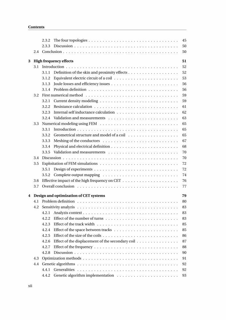
2.4 Computation of the mutual inductance. Here, two square coils with a single
closed turn are represented, but eq. (2.8) can be applied to any conductor shape. 30
2.5 Computation of the self inductance. . . . . . . . . . . . . . . . . . . . . . . . . . . 31
2.6 Top views of (a) a rectangular coil and (b) a hexagonal coil. Cross-sections of (c)
a PCB coil and (d) a coil with conventional or Litz wires. . . . . . . . . . . . . . . 34
2.7 (a) Magnetic flux densities generated by coil 5 when it is excited by a 1 A current.
Computed with the Biot-Savart’s law (a) and with the FEM software (b) at a
height of z = 5 mm. Computed with the Biot-Savart’s law (c) and with the FEM
software (d) at a height of z = 1 mm. . . . . . . . . . . . . . . . . . . . . . . . . . . 36
2.8 Self inductance computed as a function of the step size for coil 2 (a) and for coil
5 (b). . . . . . . . . . . . . . . . . . . . . . . . . . . . . . . . . . . . . . . . . . . . . 37
2.9 (a) Mutual inductance computation between coils 1 and 2. (b) Mutual induc-
tance computation between coils 5 and 6. . . . . . . . . . . . . . . . . . . . . . . 38
2.10 (a) Measured and computed mutual inductance between coils 1 and 2. (b)
Measured and computed mutual inductance between coils 5 and 6. . . . . . . . 41
2.11 Electric circuit of the coreless transformer. . . . . . . . . . . . . . . . . . . . . . . 42
2.12 (a) Step 2: Simplification of the secondary circuit. (b) Step 3: Reflected impedance
of the secondary circuit. (c) Step 4: Total equivalent impedance of the coreless
transformer. . . . . . . . . . . . . . . . . . . . . . . . . . . . . . . . . . . . . . . . . 44
2.13 (a) Series-Series (SS) topology. (b) Parallel-Series (PS) topology. (c) Series-Parallel
(SP) topology. (d) Parallel-Parallel (PP) topology. . . . . . . . . . . . . . . . . . . . 46
3.1 Equivalent electric circuit of a coil at high frequency. . . . . . . . . . . . . . . . . 53
3.2 Typical impedance of a coil versus the frequency, with hypothetical values R =1Ω, L = 5 µH, C = 10 pF (a) Real part. (b) Imaginary part. . . . . . . . . . . . . . 55
3.3 Typical variation of the resistance versus the frequency for coils 5, 7 and 10. . . 58
3.4 Typical variation of the self inductance versus the frequency for coils 5, 7 and 10. 58
3.5 Conductor of rectangular cross-section. . . . . . . . . . . . . . . . . . . . . . . . . 60
3.6 Comparison between the analytical solution and the numerical one for the linear
resistance (a) and for the linear internal inductance (b). The linear resistance
and the linear internal inductance are normalized to the DC value. . . . . . . . 63
3.7 Comparison between the numerical solution and the measurements on (a) coil
4, (b) coil 5, (c) coil 7, and (d) coil 10. . . . . . . . . . . . . . . . . . . . . . . . . . . 64
3.8 Geometrical design of a coil with Flux2d. . . . . . . . . . . . . . . . . . . . . . . . 66
3.9 Intensity of the magnetic flux density around the coil showing the boundary
condition of the design. . . . . . . . . . . . . . . . . . . . . . . . . . . . . . . . . . 67
3.10 Magnetic field lines zoomed in the conductors region. . . . . . . . . . . . . . . . 68
3.11 Meshing of the intermediate box and the conductors. . . . . . . . . . . . . . . . 69
3.12 Current density distribution in the conductors at (a) 200 kHz and (b) 5 MHz. . . 69
3.13 Comparison between measured and computed AC resistance. The AC resistance
is normalized to the DC resistance. (a) Coil 4, (b) Coil 5, (c) Coil 6, (d) Coil 7, (e)
coil 10, (f) coil 11. . . . . . . . . . . . . . . . . . . . . . . . . . . . . . . . . . . . . . 71
xvi
List of Figures
3.14 Discrepancy between FEM simulations and the complete output mapping used
with the closest pick strategy. A total of 2000 samples randomly generated in the
experimental domain have been evaluated. . . . . . . . . . . . . . . . . . . . . . 75
3.15 Discrepancy between FEM simulations and the complete output mapping with
interpolation. The results obtained from the model with interactions and with-
out interactions are compared. The same 2000 samples as in Fig. 3.14 have been
evaluated. . . . . . . . . . . . . . . . . . . . . . . . . . . . . . . . . . . . . . . . . . 76
3.16 Computed quality factor for different coils. . . . . . . . . . . . . . . . . . . . . . . 77
3.17 Efficiency and power losses versus the frequency for the coreless transformer
made of coils 5 and 6. Dashed curves show the case where the HF effects are not
taken into account, and plain curves when they are. . . . . . . . . . . . . . . . . 78
4.1 (a) Mutual inductance, (b) output power, and (c) efficiency versus the number of
primary turns and the number of secondary turns. . . . . . . . . . . . . . . . . . 84
4.2 (a) Mutual inductance, (b) output power, and (c) efficiency versus the primary
track width and the secondary track width. . . . . . . . . . . . . . . . . . . . . . . 86
4.3 (a) Mutual inductance, (b) output power, and (c) efficiency versus the primary
inter-track space and the secondary inter-track space. . . . . . . . . . . . . . . . 87
4.4 (a) Mutual inductance, (b) output power, and (c) efficiency versus the primary
coil size and the secondary coil size. . . . . . . . . . . . . . . . . . . . . . . . . . . 88
4.5 (a) Mutual inductance, (b) output power, and (c) efficiency versus the displace-
ments xd and yd of the secondary coil. . . . . . . . . . . . . . . . . . . . . . . . . 89
4.6 (a) Output power and (b) efficiency versus the operating frequency. . . . . . . . 90
4.7 Schematic description of a conventional GA. . . . . . . . . . . . . . . . . . . . . . 93
4.8 Power losses versus output power for different solutions obtained from two runs
of optimization and with different values of α. . . . . . . . . . . . . . . . . . . . . 97
4.9 Output power versus α showing the fluctuations of the solutions obtained with
the second run. . . . . . . . . . . . . . . . . . . . . . . . . . . . . . . . . . . . . . . 97
4.10 Explanation of the Pareto optimality. Here, the point D dominates the points E
and F, because its two objectives are better. A and B belong to the set of Pareto
optima, because no other solution dominates them. . . . . . . . . . . . . . . . . 98
4.11 Schematic description of the MOGA implemented for CET systems. . . . . . . . 100
4.12 Multiplication coefficient evolution. . . . . . . . . . . . . . . . . . . . . . . . . . . 104
4.13 Obtained Pareto optimal solutions with NSGAimp and Matlab’s NSGA-II on (a)
ZDT1, (b) ZDT2, (c) ZDT3, (d) ZDT4. . . . . . . . . . . . . . . . . . . . . . . . . . . 105
4.14 (a) Obtained Pareto optimal solutions with NSGAimp and Matlab’s NSGA-II on
Constr. (b) Obtained Pareto optimal solutions with NSGAimp on Tnk. . . . . . . 106
4.15 Pareto optimal solutions obtained for three successive runs of NSGAimp on the
problem Prob1. . . . . . . . . . . . . . . . . . . . . . . . . . . . . . . . . . . . . . . 106
4.16 Arrays of (a)-(b) circular coils, (c) hexagonal coils, (d)-(e) square coils. (f) Two
layers of primary square coils. . . . . . . . . . . . . . . . . . . . . . . . . . . . . . . 109
4.17 (a) Single-transistor converter. (b) Full-bridge converter . . . . . . . . . . . . . . 110
xvii

List of Figures
4.18 (a) Position P1, (b) position P2, (c) position P3. . . . . . . . . . . . . . . . . . . . . 111
4.19 (a) Position Pa , (b) position Pb , (c) position Pc . . . . . . . . . . . . . . . . . . . . 112
4.20 Results of three optimization runs giving the total output power (−O1) versus
the total Joule losses (O2). . . . . . . . . . . . . . . . . . . . . . . . . . . . . . . . . 114
5.1 The CET system for the CET notebook charger. . . . . . . . . . . . . . . . . . . . 119
5.2 (a) Top view and (b) side view of the full-bridge converter. . . . . . . . . . . . . . 121
5.3 The output rectifier with the series compensation capacitor and the smoothing
capacitor. . . . . . . . . . . . . . . . . . . . . . . . . . . . . . . . . . . . . . . . . . . 122
5.4 Measurement of the input voltage and the current in the primary coil when no
load is present. . . . . . . . . . . . . . . . . . . . . . . . . . . . . . . . . . . . . . . 123
5.5 (a) Measurement of the input voltage and the current in the primary coil when
the coreless transformer is loaded by a resistor of 5Ωwithout the rectifier. (b)
Measurement of the voltage and the current in the load. . . . . . . . . . . . . . . 124
5.6 (a) Measurement of the input voltage and the current in the primary coil when
the coreless transformer is loaded by a resistor of 5 Ω with the rectifier. (b)
Measurement of the voltage at the input of the secondary rectifier and the current
in the secondary coil. . . . . . . . . . . . . . . . . . . . . . . . . . . . . . . . . . . . 125
5.7 Efficiency and DC voltage level versus the load resistance. . . . . . . . . . . . . . 126
5.8 (a) Picture of the prototype without the notebook. (b) Picture of the prototype
while charging the notebook battery. . . . . . . . . . . . . . . . . . . . . . . . . . 127
5.9 (a) The array of 9 coils. (b) The array of 18 coils. . . . . . . . . . . . . . . . . . . . 128
5.10 Picture of the setup with the array of 18 coils. . . . . . . . . . . . . . . . . . . . . 129
5.11 Load voltage versus the displacement along X axis and along Y axis. (a) Calcu-
lated and (b) measured over an array of 9 coils. (c) Calculated and (d) measured
over an array of 18 coils distributed into two shifted layers. . . . . . . . . . . . . 130
5.12 (a) Top view and (b) bottom view of the prototype. . . . . . . . . . . . . . . . . . 132
5.13 General strategy used for the CET table. . . . . . . . . . . . . . . . . . . . . . . . . 133
5.14 Different time scales for the signals applied to the primary coils array. . . . . . . 134
5.15 Primary circuit schematic. . . . . . . . . . . . . . . . . . . . . . . . . . . . . . . . . 135
5.16 Single-transistor converter. . . . . . . . . . . . . . . . . . . . . . . . . . . . . . . . 136
5.17 (a) Good scenario with two loads and two activated coils. (b) Bad scenario with
two loads and four activated coils. . . . . . . . . . . . . . . . . . . . . . . . . . . . 137
5.18 (a) Signal generated on the gate of the MOSFET. (b) Input voltage and primary
coil current. . . . . . . . . . . . . . . . . . . . . . . . . . . . . . . . . . . . . . . . . 137
5.19 Circuit implemented for the estimation of the current. . . . . . . . . . . . . . . . 139
5.20 (a) Current generated by the voltage supply. (b) Voltage provided to the A/D
converter of the DSP. . . . . . . . . . . . . . . . . . . . . . . . . . . . . . . . . . . . 140
5.21 Current delivered by the DC voltage supply over a large time scale showing a few
short detection phases between the supply phases with no load (a), one load (b),
and two loads (c). View of the current during a single detection phase with no
load (d), one load (e), and two loads (f). . . . . . . . . . . . . . . . . . . . . . . . . 141
xviii

List of Figures
5.22 Zoom on the second coil scanning with and without load. . . . . . . . . . . . . . 142
5.23 Secondary circuit scheme for the speaker providing a 5 V (DC) output. . . . . . 142
5.24 (a) Voltage and current measured on a load of 10Ωwithout rectifier. (b) Voltage
and current measured at the input and at the output of the rectifier loaded by a
resistor of 10Ω. . . . . . . . . . . . . . . . . . . . . . . . . . . . . . . . . . . . . . . 143
5.25 Picture of the primary coils array and the secondary coil. . . . . . . . . . . . . . 145
A.1 Behavior of the coreless transformer (coils 5 and 6) when the load resistance
varies from 10 to 100Ω. . . . . . . . . . . . . . . . . . . . . . . . . . . . . . . . . . 154
A.2 Behavior of the coreless transformer (coils 5 and 6) when the load resistance
varies from 10 to 100Ω. . . . . . . . . . . . . . . . . . . . . . . . . . . . . . . . . . 155
A.3 Behavior of the coreless transformer (coils 5 and 6) when the load resistance
varies from 10 to 100Ω. (a)-(b) PS topology, (c)-(d) PP topology. . . . . . . . . . 157
A.4 Behavior of the coreless transformer (coils 5 and 6) when the load resistance
varies from 10 to 100Ω. (a)-(b) SS topology, (c)-(d) SP topology. . . . . . . . . . 158
C.1 (a) Pareto front line of (a) ZDT1, (b) ZDT2, (c) ZDT3, (d) ZDT4. . . . . . . . . . . 171
C.2 (a) Pareto front line of (a) Constr, (b) Tnk. . . . . . . . . . . . . . . . . . . . . . . . 171
D.1 Energy chain for the CET system of the notebook. . . . . . . . . . . . . . . . . . . 174
D.2 Electronic schematic from the grid to the primary coil. The secondary side is not
shown. . . . . . . . . . . . . . . . . . . . . . . . . . . . . . . . . . . . . . . . . . . . 175
D.3 Schematic view of the rectified and smoothed voltages. . . . . . . . . . . . . . . 176
D.4 Schematic view of the AC voltage at the converter output. . . . . . . . . . . . . . 177
D.5 (a) Electronic schematic of the secondary circuit. (b) Equivalent circuit. . . . . 178
D.6 (a) Top view and (b) side view of the full-bridge converter. . . . . . . . . . . . . . 179
D.7 The output rectifier with the series compensation capacitor and the filter capacitor.180
E.1 Photograph of the primary electronic circuit and a portion of the primary coils
array. . . . . . . . . . . . . . . . . . . . . . . . . . . . . . . . . . . . . . . . . . . . . 181
xix


List of Tables
1.1 Summary of the main characteristics of some CET fixed charging applications
available on the market or found in literature. The size of the coils is given by the
external diameter for the circular coils and by the external lengths for square or
rectangular coils. . . . . . . . . . . . . . . . . . . . . . . . . . . . . . . . . . . . . . 11
1.2 Summary of the main characteristics of some CET free charging systems found
in literature. The size of the coils is given by the external diameter for the circular
or hexagonal coils and by the external lengths for square or rectangular coils. . 18
2.1 Calculated DC internal self inductance for conductors of rectangular cross-
section with different aspect ratios. . . . . . . . . . . . . . . . . . . . . . . . . . . 31
2.2 Geometric parameters . . . . . . . . . . . . . . . . . . . . . . . . . . . . . . . . . . 34
2.3 Characteristics of the experimental coils . . . . . . . . . . . . . . . . . . . . . . . 35
2.4 Self inductance computations as a function of the step size. . . . . . . . . . . . . 37
2.5 Computation time for different cases issued from Fig. 2.9(b). . . . . . . . . . . . 38
2.6 Results of the self inductance computations and measurements . . . . . . . . . 39
2.7 Results of the mutual inductance computations and measurements. . . . . . . 40
2.8 Electric parameters. . . . . . . . . . . . . . . . . . . . . . . . . . . . . . . . . . . . 41
3.1 Input parameters for the FEM simulations . . . . . . . . . . . . . . . . . . . . . . 66
3.2 Variation range of the input parameters . . . . . . . . . . . . . . . . . . . . . . . . 73
4.1 Free parameters of CET systems. . . . . . . . . . . . . . . . . . . . . . . . . . . . . 82
4.2 Free parameters. . . . . . . . . . . . . . . . . . . . . . . . . . . . . . . . . . . . . . 107
4.3 Output parameters. . . . . . . . . . . . . . . . . . . . . . . . . . . . . . . . . . . . . 107
4.4 Electric specifications of the mouse, keyboard and loudspeaker . . . . . . . . . 108
4.5 Input parameters for the CET table. . . . . . . . . . . . . . . . . . . . . . . . . . . 114
4.6 Output parameters for the CET table. . . . . . . . . . . . . . . . . . . . . . . . . . 114
5.1 Specifications of the CET notebook charger demonstrator . . . . . . . . . . . . . 118
5.2 Final design of the coreless transformer for the Notebook. . . . . . . . . . . . . . 120
5.3 Calculated and measured parameters of the coreless transformer. . . . . . . . . 120
xxi

List of Tables
5.4 Electrical values of the coreless transformer. . . . . . . . . . . . . . . . . . . . . . 123
5.5 Electrical values of the coreless transformer. . . . . . . . . . . . . . . . . . . . . . 124
5.6 Electrical values of the coreless transformer. . . . . . . . . . . . . . . . . . . . . . 125
5.7 Geometrical parameters of the coils for the second prototype. . . . . . . . . . . 131
5.8 Power and efficiency measurements . . . . . . . . . . . . . . . . . . . . . . . . . . 144
5.9 Parameters of the primary and secondary coils . . . . . . . . . . . . . . . . . . . 145
5.10 Measured and calculated electric parameters of the third prototype. . . . . . . . 146
5.11 Estimation of the magnetic flux density at different points above the two CET
prototypes. . . . . . . . . . . . . . . . . . . . . . . . . . . . . . . . . . . . . . . . . . 147
C.1 Unconstrained test functions that are often used to evaluate MOGAs. . . . . . . 170
C.2 Constrained functions that are often used to evaluate MOGAs. . . . . . . . . . . 170
D.1 Main components of the full-bridge converter . . . . . . . . . . . . . . . . . . . . 178
D.2 Components used in the rectifier. . . . . . . . . . . . . . . . . . . . . . . . . . . . 180
E.1 Description of the main components used in the primary circuit. . . . . . . . . 182
E.2 The main components used in the detection circuit. . . . . . . . . . . . . . . . . 182
E.3 Description of the main components used in the primary circuit. . . . . . . . . 183
xxii

CHAPTER 1
Introduction
Summary1.1 Contactless energy transfer . . . . . . . . . . . . . . . . . . . . . . . . . . . . . 2
1.2 Scope of the thesis . . . . . . . . . . . . . . . . . . . . . . . . . . . . . . . . . . 3
1.2.1 Historical context and current state . . . . . . . . . . . . . . . . . . . . . 3
1.2.2 Technical and industrial background . . . . . . . . . . . . . . . . . . . . 4
1.3 State of the art . . . . . . . . . . . . . . . . . . . . . . . . . . . . . . . . . . . . . 5
1.3.1 Fixed position systems . . . . . . . . . . . . . . . . . . . . . . . . . . . . . 6
1.3.2 Free position systems . . . . . . . . . . . . . . . . . . . . . . . . . . . . . 12
1.3.3 Discussion . . . . . . . . . . . . . . . . . . . . . . . . . . . . . . . . . . . . 19
1.4 Motivations and objectives . . . . . . . . . . . . . . . . . . . . . . . . . . . . . 19
1.5 Thesis structure . . . . . . . . . . . . . . . . . . . . . . . . . . . . . . . . . . . . 20
This first chapter gives the general aspects related to this thesis. The first section introduces
the reader to the world of contactless energy transfer (CET), through a large panel of different
technologies associated to CET and then by focusing on the most interesting one for this
thesis, that is electromagnetic coupling. An overview of the commercially available devices
and a state of the art of the recent researches are summarized in the second part of the chapter.
Then, the strategy and the main objectives for designing and optimizing CET systems are
described. Finally this first chapter ends with the outline of the whole dissertation.

Chapter 1. Introduction
1.1 Contactless energy transfer
Contactless Energy Transfer refers to a really broad and vague concept if not bounded by a
specific context. In its large meaning, contactless energy can take the form of electricity, light,
heat or even sound and wind. The contactless transfer involves a starting point (source) and
an ending point (receiver) without intermediate material that would be intentionally added
to achieve some purpose. In the scope of this thesis, the starting and ending points are both
characterized by electric energy, with in between no additional wires or material.
Light energy transfer can be obtained by photons travel from a source such as the sun or a
laser, to a receiver that is generally a photovoltaic cell. The advantage of the laser as a source
is that it provides a very directional illumination thanks to its high degree of temporal and
spatial coherence. However, the efficiency of light energy transfer is very low, because the
losses at each step of the transfer processes are important, namely in the source, in the air
and in the receiver. Furthermore, the economical aspects are not attractive [45]. For these
reasons, light energy is interesting only for applications that require a transfer over a very large
distance, for example in the space.
The microwaves can also transfer energy over a relatively large distance that can be greater
than the emitter and receiver sizes. They are electromagnetic waves ranging from 1 GHz
to 300 GHz and are used for far-field energy transfer [83]. The most common source for
domestic applications is the magnetron thanks to its unexpensive cost, but high frequency
waves can be also generated by antennas. The receiver is a rectenna which is actually an
antenna with a rectifier used to convert microwaves into DC electricity. The main drawbacks
of this technology are the health risks and the relatively low efficiency that can be obtained.
The most used way to transfer contactless energy is the magnetic induction whose principle is
shown in Fig. 1.1. It uses near-field electromagnetic waves in the range of frequencies between
10 kHz and a few MHz. The characteristic distance of transfer is the same order as the size of
the receiver (secondary coil) and the emitter (primary coil). Such CET systems are based on
the coreless transformers theory. The working principle consists in applying a high frequency
current in a primary coil. In the surrounding air, it generates a magnetic field that induces a
voltage to a secondary coil if placed in proximity. It is necessary to operate at high frequency
because coreless transformers suffer from weak mutual coupling. To enhance the coupling
between primary and secondary, both coils must be well aligned and the air gap must be as
small as possible.
With this description, a distinction can be made between inductive CET and RFID systems.
Indeed, the former involves a transfer of power through a relatively short distance as de-
fined above, while the latter is used to transfer information (with power generally lower than
2

1.2. Scope of the thesis
100 mW) through a large distance.
I1U1
B
I1U1
Figure 1.1: Principle of contactless energy transfer by induction.
1.2 Scope of the thesis
1.2.1 Historical context and current state
Nicola Tesla proposed the first theories of CET in 1899-1900. He carried out various wireless
transmission and reception experiments through air or matter. At his Colorado Springs
laboratory, he experimented for example a remote supply of 200 light bulbs through the
ground from a distance of about 40 km [14].
The first reported researches on the so-called energy transport by inductive coupling date
from the 1960s [71]. Although the principle of inductive CET was known for a long time,
this technology has remained immature for a long time as the first industrial applications
appear in the 1990s with the electric toothbrushes. Even nowadays the number of electric
devices supplied by inductive CET is relatively low. This absence is probably due to the lack of
standards and regulations for this technology, and also to the uncertainty from the average
population concerning the inherent health dangers.
In 1998, a scientific committee has published general guidelines [25] to avoid any kind of
health risks concerning the exposure of the population to electromagnetic fields. Basically
these recommendations provide the restrictions for the public exposure as a function of the
operating frequency, the immersed body proportion and the size of the coils. However, in
practice, they are not relevant according to [10]. Therein, a study on the maximum power
transfer, based on these restrictions, shows that common applications including coils size of
40 mm to 100 mm could transfer no more than about 30 mW, which is roughly two orders of
3

Chapter 1. Introduction
magnitude lower than existing products on the market. This statement will be assessed later
in this thesis work.
In late 2008, the Wireless Power Consortium (WPC) has been created in order to unify the
powering protocols related to inductive CET systems. At that time the consortium consisted
of the gathering of 8 companies that are active in the domain of CET technologies. Thanks
to its great success, it counted 100 companies in October 2011. Basically the WPC aims to
set the standard for interoperable wireless charging [18]. In July 2010, a three-part document
has been finalized, in which the new standard, called ’Qi’, is designed for electronic devices
up to 5 W. Practically it means that all receivers stamped with the Qi logo can be supplied
by all transmitters also stamped with the same logo. In this sense the Qi sign stands for the
emblematic figure of interoperability and compatibility between the different devices.
1.2.2 Technical and industrial background
More and more electric applications require an energy transfer without wires and contacts.
Especially in the domain of desktop applications such as computer peripherals, wireless
technologies (Bluetooth, ZigBee, RF, IR, WiFi) that allow transfer of information are very trendy,
while the supplying process uses massively wires or batteries. In a desktop environment,
removing the cables between the power source and electronic devices would be convenient. It
would allow to gain a certain amount of place and to clean the surface from wires pollution.
In this context, the contactless energy transfer by inductive coupling meets more and more
success. Some products are already available for a few applications, such as mice or mobile
phones. However, a full platform enabling to supply simultaneously several consumers is still
not to be reported.
In the framework of a collaboration between Logitech SA and the Laboratory of Integrated
Actuators (LAI), CET systems are studied for notebook and desktop applications.
This collaboration is divided into two different practical applications:
1. The inductive notebook charger is aiming to realize the prototype of a CET system
from a platform to a static notebook. The said platform is a product already available on
the market under the commercial name Alto (Fig. 1.2);
2. The CET table is aiming to realize a prototype of a CET system embedded in a table in
order to supply multiple desktop peripherals.
Logitech [9] is a Swiss company developing and marketing products such as peripheral devices
for PCs, including mice, keyboards, loudspeakers, microphones and webcams. They are
4

1.3. State of the art
(a) (b)
Figure 1.2: Pictures of the Alto platform. (a) Without notebook [1]. (b) Withnotebook [2].
responsible in the above-mentioned projects for providing the equipment (Alto platform,
peripherals, . . . ) and sharing their know-how on hardware and manufacturing of electronic
peripherals.
The LAI has conducted numerous projects linked to CET. As representative examples, a few
projects are chosen and briefly described here. The first one is the Serpentine project [55],
[56]. A power of 2.5 kW was provided to an electric vehicle through a coreless transformer
composed of a linear track of primary coils and a single secondary coil.
The second application concerns a project in collaboration with Hilti [29]. The goal was to add
new functions to a drill machine, such as a bidirectional communication between the main
tool and the accessories. The main challenge was to simultaneously transfer power (25 W) and
information. Therefore two pairs of windings were used with extremely low mutual effects in
order to make both functions as decoupled as possible.
The third application refers to the ColoStim project. The goal of the project was to electrically
stimulate the colon of people suffering from severe motility troubles. Using classical electric
stimulators often causes problems due to the presence of wires. In order to resolve this
problem, a new device using inductive CET is designed in [57], [58]. The primary is worn
around the patient’s torso and multiple secondary windings (0.1 W) are implanted all along
the colon so as to stimulate the peristaltic waves.
1.3 State of the art
CET systems can be classified into two categories. The first one concerns fixed position
systems wherein the devices to be supplied are static. The second one concerns the free
5

Chapter 1. Introduction
position systems involving devices that can be freely moved on the charging surface. With
such a definition, it is obvious that the inductive notebook charger belongs to the first one and
the CET table to the second one.
1.3.1 Fixed position systems
The fixed position system is the simplest inductive CET method. Nowadays, it involves almost
all the existing industrial applications. It usually charges one load and the energy is transferred
from a single primary coil to a single secondary coil. Furthermore, both coils have to be
approximatively the same size and well aligned to ensure a good mutual coupling, a sufficient
amount of transferred energy and a good efficiency.
Induction cookers
Fixed CET is traditionally the method used in induction cookers, except that the secondary
coil is replaced by the cooking vessel made of ferromagnetic and conductive metal. The initial
researches and patents date from the early 1900s, but the first production of induction cookers
was performed in the 1970s by the Westinghouse Electric Corporation [15]. Nowadays, many
manufacturers are present on this market, such as Bosch, Miele, Siemens, Electrolux,. . .
The principle of the induction heating is shown in Fig. 1.3. The magnetic field generated
by the primary coil creates Eddy currents in the pot that cause the heating Joule effect. The
wires of the primary coils generally exhibit a flat and spread geometry in order to enhance the
distribution of the magnetic field that reaches the cooking vessel. The transferred power is in
the order of 1 to 2 kW and the operating frequency is situated in a range from 20 kHz to 50 kHz.
Figure 1.3: Principle of an induction cooker.
6

1.3. State of the art
Electric toothbrushes
Inductive CET is interesting for applications that require no exposed electrical contacts, such
as devices that are used in a moist environment or even immersed in water. Since the early
1990s, rechargeable toothbrushes (for example from the Oral-B brand [7]) use this technology
that allows to enclose and therefore fully insulate the wires. It gives the advantage to protect
the user against electric shocks due to apparent contacts and to prevent short-circuits that
could damage electronics. The system generally includes a ferromagnetic core that increases
the coupling between the coils. The operating frequency is around 10 kHz or more, and the
transferred power is between 10 and 15 W. Similar CET systems are also integrated into electric
shavers.
Transcutaneous energy transfer
In the medical domain, CET can be used to supply surgically implanted devices, where it is
specifically called transcutaneous energy transfer (TET).
For instance, the use of heart assist devices to circumvent left ventricular dysfunctions has
been proven to be beneficial for the patients [101]. However, conventional ways to supply
them can develop additional risks associated to the apparition of infections as the wires are
passed through the skin. To solve this problem, a novel resonant converter with its coreless
transformer is designed in [129] and allows to supply a prototype of such a heart assist device.
The amount of transferred power is 10 W and the operating frequency is 205.1 kHz.
In [86],[87], a TET system is designed for an implantable artificial heart. Therein, the main
constraint is that the primary coil has to be placed near the secondary one in order to have
a good coupling. The operating frequency is 50 kHz and the amount of transferred power is
20 W. The coreless transformer includes two circular spiral coils whose mechanical structure
is maintained by radial amorphous fibers. These fibers make the coils flexible and contain
magnetic material that is supposed to improve the energy transfer by concentrating the flux
through the coils (c.f. Fig. 1.4(a)). Furthermore, a special focus is made on the temperature
rise of the secondary coil, which is a critical issue for in vivo applications.
Finally, TET is used in [105] to supply electrodes that aim to generate electrical stimulations in
order to restore the movement of limbs paralysed by injured spinal cord. The primary coil has
a solenoid shape and is placed around the said limb. The secondary coils have spiral shapes
and are connected to the electrodes, as shown in Fig. 1.4(b). Two different frequencies of
96 kHz and 387 kHz are tested, and the transferred power is not indicated but estimated to be
less than 1 W for each electrode.
7

Chapter 1. Introduction
(a) (b)
Figure 1.4: (a) Coreless transformer structure of the TET system for artificial heartsupply, showing the amorphous magnetic coils [87]. (b) Coreless transformerstructure of the TET for the electrical stimulation system [105].
Desktop peripherals and mobile phones
The first CET studies dedicated to mobile phones were realized in the early 2000s. For example,
the prototype of a small platform allowing to recharge a mobile phone battery is proposed in
[33], [34]. A picture of the prototype is given in Fig. 1.5(a). The coreless transformer is made of
printed circuit board (PCB) coils that have to be precisely aligned to start the charging process.
The operating frequency is ranged between 920 and 980 kHz, and the power transferred to the
battery is 3.3 W, but the transformer has been tested to transfer up to 24 W.
More recently, many desktop applications have been marketed. An example of existing CET
application is the battery-free optical mouse from A4 Tech [8] (c.f. Fig. 1.5(b)). Instead of
batteries, the mouse uses inductive CET to provide energy via the included mouse pad, which
is connected to a computer USB port. Mice are very low powered devices, generally the
amount of transferred power is less than 1 W. In a similar way, the HP Touchstone is a small
dockstation powered by the USB port and can transfer the power (5 W) to recharge a phone or
a Palm device [6].
Concerning systems involving CET to multiple devices, many products are commercially
available. They remain in this category of fixed position charging because they do not offer
the possibility to supply the devices freely placed on the whole surface, but only at predefined
places. For example, the first CET table developed by Fulton Innovation under the denomina-
tion of eCoupled allows to transfer energy to multiple but fixed devices [5]. This application
has the ability to communicate with the devices thanks to a process specifically developed
by Fulton, which allows to transfer the exact amount of power required by each load on the
8

1.3. State of the art
platform.
Other companies are present on this market with similar platforms and applications, such
as Qualcomm with the eZone charger [16], Mojo Mobility with the MojoPad [17], Homedics
with its Powermat product line [12]. The common points to these applications are the low
power devices that they can supply (generally less than 5 W), the predetermined position of
the devices on the platform and the integrated intelligence that detects and recognizes the
devices.
(a) (b)
(c)
Figure 1.5: (a) One of the first prototypes involving a CET system to charge amobile phone [34]. (b) Inductively charged mouse from A4 Tech [8]. (c) PortablePowermat station that allows to charge up to three devices simultaneously.
Electric vehicles
A new niche market that may explode in the future for fixed positioning CET systems is the
electric vehicles charging. Many researches are ongoing in this domain [49], [127], [124],
prototypes are being tested by Siemens or BMW [4], and some applications are on the verge
to be commercially available [3], [19]. For instance, the typical specifications for a prototype
(such as the one developed in [127]) consist of transferring a power of 30 kW to the vehicle
9

Chapter 1. Introduction
battery. The operating frequency is 20 kHz. The main issue here comes from the large airgap
of 45 mm which makes the coupling low.
As a conclusion for the fixed position systems, a summary of the most noteworthy applications
encountered in this section is given in Table 1.1 with their main specifications. A remark
should be made about the efficiency of such CET systems. Strangely, efficiency issues are
rarely discussed in literature, especially for low-consuming applications. It is probably due
to the fact that it is not an attractive point for inductive CET. Furthermore, when they are
mentioned, their application is often blurry and it is difficult to determine what they take
into account. Thereby, the efficiency is just mentioned in parentheses in table 1.1 when the
information is available and the values have to be taken with caution.
10

1.3. State of the art
Tab
le1.
1:Su
mm
ary
of
the
mai
nch
arac
teri
stic
so
fso
me
CE
Tfi
xed
char
gin
gap
pli
cati
on
sav
aila
ble
on
the
mar
ket
or
fou
nd
inli
tera
ture
.Th
esi
zeo
fth
eco
ils
isgi
ven
by
the
exte
rnal
dia
met
erfo
rth
eci
rcu
lar
coil
san
db
yth
eex
tern
alle
ngt
hs
for
squ
are
or
rect
angu
lar
coil
s.
Ap
pli
cati
on
Au
tho
r/
Co
mp
any
Ref
.Ye
arC
oil
sFr
equ
.P
ower
Spec
ifics
Ind
uct
ion
coo
k-er
sW
esti
ngh
ou
seC
orp
.[1
5]19
73-1
975
Cir
cula
r-
spir
al~
150-
300
mm
20-5
0kH
z1-
2kW
(η=
84%
)N
ose
con
dar
yco
ilFe
rro
mag
net
icm
etal
Ele
ctri
cto
oth
-b
rush
esO
ral-
BP
hil
ips
Son
icar
e[7
],[1
1]~
1990
Cir
cula
r-
squ
are
~20
mm
10kH
z10
-15
WFe
rro
mag
net
icco
re
Tran
scu
tan
eou
sen
ergy
tran
sfer
Wu
etal
.[1
29]
2009
Litz
wir
esC
ircu
lar
~20
-30
mm
205.
1kH
z10
W(η
=84
.5%
)-
Mat
suki
etal
.[8
6],[
87]
1990
-199
2C
ircu
lar
-sp
iral
114
mm
50kH
z20
W(η
=90
%)
Flex
ible
coil
sR
adia
lmag
net
icfi
ber
s
Sato
etal
.[1
05]
2001
Pri
mar
yC
ircu
lar
-so
len
oid
55m
m96
kHz
<1
WP
rim
ary
coil
aro
un
dth
ear
m
Seco
nd
ary
Cir
cula
r-
spir
al11
.5m
m
Des
kto
pp
erip
her
als
Mo
bil
ep
ho
nes
Ch
oie
tal.
[34]
2004
PC
Bco
ils
Cir
cula
r-
spir
al35
mm
920-
980
kHz
24W
(η=
57%
)-
A4
Tech
[8]
-C
ircu
lar
~20
0m
m(P
rim
.)~
30m
m(S
ec.)
-<
1W
Pri
mar
yco
ilsu
pp
lied
by
USB
po
rt
Pow
erm
at[1
2]-
Squ
are
~10
mm
-<
5W
Up
toth
ree
dev
ices
si-
mu
ltan
eou
sly
char
ged
Ele
ctri
cve
hi-
cles
Wan
get
al.
[127
]20
05R
ecta
ngu
lar
800×
600
mm
220
kHz
30kW
Larg
eai
rga
p
11

Chapter 1. Introduction
1.3.2 Free position systems
The free position systems are more complex and elaborated than the fixed ones. They generally
can charge one or multiple loads on a large area, whatever their position. They are made of
multiple primary and secondary coils that can be distributed in one or multiple layers. Besides,
they often integrate a detection system that allows to activate only the primary coils located
under the loads. Until now, no such manufactured system does exist, but many projects are in
the research phase.
Single primary coil configuration
At first thought, the most simplistic way to supply multiple loads that can be freely moved
on a large surface consists in using a single primary coil that encompasses the whole useful
area. However, this leads to two main problems. First, it is difficult to ensure that the same
amount of energy is transferred for every position of the loads. Secondly, as the primary coil
is much larger than the secondary ones, their coupling is very low which obviously makes it
more difficult to transfer large amounts of energy.
In [77], such a system is proposed to transfer simultaneously from 2 to 12 W to four loads at
an operating frequency of 418 kHz. The design of the primary coil is based on a magnetic
field approach. Indeed the intensity of the magnetic field is almost uniform thanks to the use
of two layers of primary coils different in shape and size. The main drawback of this design
procedure comes from the relatively small charging surface that has to be limited in order to
ensure a sufficient power to be transferred. The prototyped primary platform has a size of
126 mm × 97 mm and the secondary coils have a size of 60 mm × 30 mm.
Two-dimensional primary coils
Unlike the electric vehicles presented in section 1.3.1, CET can be used to supply the vehicles
while they are moving. It allows to remove or drastically reduce the weight of the batter-
ies. These CET systems generally integrate a track of primary coils wherein the vehicle is
constrained to remain.
In [82] a study linked to the Serpentine project is conducted. A power of 2.5 kW is transferred
at about 100 kHz to an electric vehicle through a coreless transformer composed of a linear
track of primary coils (placed in the ground) and a single secondary coil (placed at the vehicle
chassis). The structure of the coreless transformer is shown in Fig. 1.6(a). The supply strategy
consists in activating only the two primary coils that are closest to the secondary one, and
the operating frequency is continuously adapted thanks to a maximum power point tracking
12
1.3. State of the art
(MPPT) method.
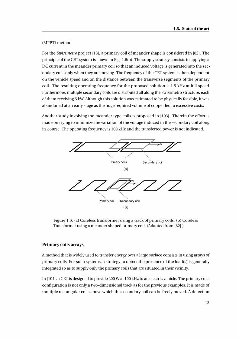
For the Swissmetro project [13], a primary coil of meander shape is considered in [82]. The
principle of the CET system is shown in Fig. 1.6(b). The supply strategy consists in applying a
DC current in the meander primary coil so that an induced voltage is generated into the sec-
ondary coils only when they are moving. The frequency of the CET system is then dependent
on the vehicle speed and on the distance between the transverse segments of the primary
coil. The resulting operating frequency for the proposed solution is 1.5 kHz at full speed.
Furthermore, multiple secondary coils are distributed all along the Swissmetro structure, each
of them receiving 5 kW. Although this solution was estimated to be physically feasible, it was
abandoned at an early stage as the huge required volume of copper led to excessive costs.
Another study involving the meander type coils is proposed in [103]. Therein the effort is
made on trying to minimize the variation of the voltage induced in the secondary coil along
its course. The operating frequency is 100 kHz and the transferred power is not indicated.
V
V
Primary coil Secondary coil
Primary coils Secondary coil
(a)
V
V
Primary coil Secondary coil
Primary coils Secondary coil
(b)
Figure 1.6: (a) Coreless transformer using a track of primary coils. (b) CorelessTransformer using a meander shaped primary coil. (Adapted from [82].)
Primary coils arrays
A method that is widely used to transfer energy over a large surface consists in using arrays of
primary coils. For such systems, a strategy to detect the presence of the load(s) is generally
integrated so as to supply only the primary coils that are situated in their vicinity.
In [104], a CET is designed to provide 200 W at 100 kHz to an electric vehicle. The primary coils
configuration is not only a two-dimensional track as for the previous examples. It is made of
multiple rectangular coils above which the secondary coil can be freely moved. A detection
13
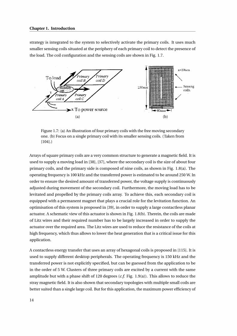
Chapter 1. Introduction
strategy is integrated to the system to selectively activate the primary coils. It uses much
smaller sensing coils situated at the periphery of each primary coil to detect the presence of
the load. The coil configuration and the sensing coils are shown in Fig. 1.7.
(a) (b)
Figure 1.7: (a) An illustration of four primary coils with the free moving secondaryone. (b) Focus on a single primary coil with its smaller sensing coils. (Taken from[104].)
Arrays of square primary coils are a very common structure to generate a magnetic field. It is
used to supply a moving load in [38], [37], where the secondary coil is the size of about four
primary coils, and the primary side is composed of nine coils, as shown in Fig. 1.8(a). The
operating frequency is 100 kHz and the transferred power is estimated to be around 250 W. In
order to ensure the desired amount of transferred power, the voltage supply is continuously
adjusted during movement of the secondary coil. Furthermore, the moving load has to be
levitated and propelled by the primary coils array. To achieve this, each secondary coil is
equipped with a permanent magnet that plays a crucial role for the levitation function. An
optimisation of this system is proposed in [39], in order to supply a large contactless planar
actuator. A schematic view of this actuator is shown in Fig. 1.8(b). Therein, the coils are made
of Litz wires and their required number has to be largely increased in order to supply the
actuator over the required area. The Litz wires are used to reduce the resistance of the coils at
high frequency, which thus allows to lower the heat generation that is a critical issue for this
application.
A contactless energy transfer that uses an array of hexagonal coils is proposed in [115]. It is
used to supply different desktop peripherals. The operating frequency is 150 kHz and the
transferred power is not explicitly specified, but can be guessed from the application to be
in the order of 5 W. Clusters of three primary coils are excited by a current with the same
amplitude but with a phase shift of 120 degrees (c.f. Fig. 1.9(a)). This allows to reduce the
stray magnetic field. It is also shown that secondary topologies with multiple small coils are
better suited than a single large coil. But for this application, the maximum power efficiency of
14

1.3. State of the art
(a) (b)
Figure 1.8: (a) Secondary coil above nine primary coils [37]. (b) Contactless planaractuator with a manipulator for different applications such as measurement,inspection or manufacturing tasks on the moving platform [39].
13% is relatively low. In [114], they still use their three-phase configuration to reduce the stray
magnetic field, but change the strategy of the CET by using larger secondary coils than the
primary ones, which ensures a larger minimal mutual coupling. Furthermore, the efficiency
and power transfer are slightly improved. The operating frequency is increased to 2.77 MHz
and it is possible to transfer up to 8 W to the loads.
(a) (b)
Figure 1.9: (a) Schematic view of the CET desktop showing the clusters of threeactivated primary coils, each of them being 120 shifted in phase [115]. (b) Thearray of primary hexagon spiral windings used in the prototype of the CET desktoppresented in [114].
In [62], a completely different design for a CET desktop is presented. The primary is composed
of an array of small circular coils. The energy is transferred from multiple primary coils to
a larger secondary one. The detection strategy consists in sending information from the
secondary to the primary. To detect the secondary device, the primary coils turn into a signal-
reception mode and the secondary coil changes into a signal-emission mode to determine its
15

Chapter 1. Introduction
exact position. Two different frequencies are used. The detection system works at 500 kHz
and the power transfer at 100 kHz. Up to 50 W can be transferred this way. The measurements
show a CET efficiency of 85%±5% depending on the location of the secondary. However,
the major drawback comes from the detection system, since it needs the integration of more
electronics on the secondary device, which is inconvenient for small peripherals.
Finally, in [130],[131], another structure for the primary coils array is proposed. A study on
the best arrangement of shapes for primary and secondary coils is performed. It aims to
ensure a good efficiency, whatever the position of the device. As a result, this paper states
that the best solution is an hexagonal packing of circular primary windings coiled around a
ferrite core, and a larger secondary circular spiral coil designed so that it covers at least one
primary coil wherever it is placed on the surface. The system is able to detect the device and
generate the charging magnetic field only within the covered area of the secondary coil. The
operating frequency is 150 kHz and the transferred power is 5 W. Practical measurements show
an efficiency in the range of 86% to 89%. A picture of the prototype is given in Fig. 1.10. On
the one hand this system is convenient because it needs only one primary layer, but on the
other hand it requires a three-dimensional ferromagnetic structure that cannot be realized
with PCB coils.
(a) (b)
Figure 1.10: Pictures of the prototype used for the measurements made in [131].(a) Primary array showing the ferrite cores inside each primary coil. (b) Secondarycoil with the ferrite plate.
Multiple layers of primary coils arrays
In single layered primary coils arrays, the main difficulty comes from the drop of magnetic
field intensity between the coils, which may lead to an insufficient amount of energy transfer if
the secondary coil is located just at this position. Using multiple layers of primary coils arrays
allows to circumvent this problem.
16

1.3. State of the art
For example, in [24] a study on different array structures is shown. Two shapes (square and
hexagonal) are taken into account, and different multilayer arrangements are tested. This
paper presents only a preliminary study on the best primary coil array structures for a battery
charging platform, so that no power or frequency considerations are investigated. The result
shows that three layers of shifted hexagonal coils or two layers of shifted square coils are the
best solutions. However, although simulations provide interesting results, the experimental
measurements remain quite far from simulations.
In order to generate an uniform flux density over the whole surface, a three-layer array of
hexagonal PCB coils (Fig. 1.11(a)) is simulated and measured in [67], [78]. This application is
designed to charge different electronic devices such as mobile phones or Palm devices. The
transferred power is about 5 W at a 130 kHz frequency. An interesting development concerns
the connexions and the activation strategy of the primary coils. Multiple coils, that belong
to one or different layers, are connected in series. Thereby, clusters of primary coils can be
activated. For example they propose so-called columns of six coils spread over two layers, and
each column can be separately activated. This simplifies the modeling and the supply of their
CET platform. A picture of a prototype is given in Fig. 1.11(b).
(a) (b)
Figure 1.11: (a) Three layers of hexagonal coils used for the modeling and simula-tion in [78]. (b) Picture showing a mobile phone being charged by a three-layerprimary coils array (taken from [67]).
As a conclusion for the free position systems, a summary of the most noteworthy applications
encountered in this section is given in Table 1.2 with their main specifications. Concerning
efficiency issues, the same remark as for Table 1.1 can be made. The values of efficiency are
given in parentheses when they are available and have to be considered with caution.
17

Chapter 1. IntroductionTa
ble
1.2:
Sum
mar
yo
fth
em
ain
char
acte
rist
ics
ofs
om
eC
ET
free
char
gin
gsy
stem
sfo
un
din
lite
ratu
re.
Th
esi
zeo
fth
eco
ils
isgi
ven
by
the
exte
rnal
dia
met
erfo
rth
eci
rcu
lar
or
hex
ago
nal
coil
san
db
yth
eex
tern
alle
ngt
hs
for
squ
are
or
rect
angu
lar
coil
s.
Syst
emA
uth
or
Ref
.Ye
arP
rim
.co
ils
Sec.
coil
sFr
equ
.P
ower
Spec
ifics
Sin
gle
pri
mar
yco
ilLi
uet
al.
[77]
2008
Rec
tan
gula
r12
6×
97m
m2
Rec
tan
gula
r60
×30
mm
241
8kH
z2-
12W
(η=
80%
)U
pto
fou
rlo
ads
sim
u-
lata
no
usl
ych
arge
d
2Dco
ils
Mac
abre
yet
al.
[82]
,[55
]19
97R
ecta
ngu
lar
1×
0.3
m2
Rec
tan
gula
r0.
9×
0.3
m2
~10
0kH
z2.
5kW
(η=
95%
)La
rge
airg
apof
55m
m
Mac
abre
yet
al.
[82]
1998
Mea
nd
erty
pe
Wid
th:0
.3m
Hal
fper
iod
:1m
Rec
tan
gula
r1×
0.3
m2
~1.
5kH
z5
kWLa
rge
airg
apof
50m
m
Pri
mar
yco
ilsar
rays
On
ela
yer
Sato
etal
.[1
04]
1996
Rec
tan
gula
r25
0×
80m
m2
Cir
cula
r80
mm
100
kHz
200
W(η
=~80
%)
Smal
lsen
sin
gco
ils
atth
ep
erip
her
yo
fpri
m.
and
sec.
coil
s
de
Bo
eije
tal.
[37]
2006
Squ
are
60m
mSq
uar
e13
0m
m10
0kH
z~
250
W(η
=95
%)
Per
man
ent
mag
net
sin
sid
eth
ese
c.co
ils
Son
nta
get
al.
[114
]20
08H
exag
on
al25
mm
Hex
ago
nal
40m
m2.
77M
Hz
≤8
WP
CB
coil
s
Hat
anak
aet
al.
[62]
2002
Cir
cula
rC
ircu
lar
100
kHz
50W
(η=
85%
)-
Zh
on
get
al.
[130
],[1
31]
2002
Cir
cula
r~
22m
mC
ircu
lar
~8
mm
150
kHz
5W
(η=
85%
)
Lar
ger
sec.
coil
sth
anp
rim
.on
esFe
rro
mag
net
icst
ruc-
ture
s
Pri
mar
yco
ilsar
rays
Mu
ltip
lela
yers
Ach
terb
erg
etal
.[2
4]20
08
Squ
are
30m
mh
exag
on
al30
mm
Hex
ago
nal
35m
m10
kHz
-P
CB
coil
s
Hu
ieta
l.[6
7],[
78]
2007
Hex
ago
nal
36m
mH
exag
on
al36
mm
195
kHz
1.5-
4W
PC
Bco
ils
18

1.4. Motivations and objectives
1.3.3 Discussion
Beyond the technical aspects, this section shows that there is no limit to the scope of the
coils shape and configuration. They can be of meander type or of spiral type, planar or
three-dimensional. Many shapes exist, such as circular, square, rectangular, hexagonal,. . . and
nothing prevents from possibly generating new exotic geometries. They can be made of usual
wires, Litz wires or PCB tracks. In array configurations, the coils can be placed in different
arrangements and in different number of layers. This diversity gives a huge freedom to the
designer, which is both an advantage and a challenge. The former because it opens the field
of research into an infinite panel of possibilities, and the latter because it is impossible to
consider every possibility.
Fortunately, this state of the art also highlights the limitations of different CET methods and
therefore can orient towards the most favorable solutions. For fixed position charging, the
most appropriate technique consists, with regard to the different presented applications, in
using one primary coil and one secondary coil that are similar in shape and in size. This
provides a high magnetic coupling which is the prerequisite to transfer the maximal power
with a good efficiency.
For the free position charging, primary coils arrays are the most appropriate solution, and
using larger secondary coils is interesting since it allows to integrate only one of them to each
load, instead of multiple smaller ones. Furthermore, the PCB support without the addition of
ferromagnetic structures offers, in our opinion, a great manufacturing benefit.
1.4 Motivations and objectives
As pointed out in the state of the art of the last section, an industrial application of a fully
operational desktop able to supply multiple peripherals over a large area does not exist yet.
The main goal of this thesis is to propose a design methodology of such CET systems.
Furthermore, optimizations for CET systems do exist but are only applicable to specific
and isolated cases. This work aims to propose a design methodology that integrates an
optimization of CET systems. With the developments presented in this thesis, it should
be possible to perform an optimal CET design for different ranges of power, different coils
configurations and different distances between the primary and secondary coils.
To be optimal, the CET system has to minimize losses in the coils and in the electronic
components. Therefore, the resistance of the coils has to be accurately modeled in order to
determine the inherent losses. This leads to issues linked to the use of high frequency currents
in the coreless transformers, namely the skin effect and the proximity effect. These effects
19

Chapter 1. Introduction
are responsible for an increase of the resistance of the coils with the frequency. However they
are most often neglected in the literature concerning CET systems design, and when they are
taken into account, some assumptions are made that are difficult to justify for optimization
purposes. Therefore an accurate modeling of these effects and their impact on the resistance
of the coils is necessary to achieve an effective optimization.
With the coreless transformers and the high frequency effects accurately modeled, an opti-
mization method can be used. For CET systems, the number of parameters that are involved is
relatively high, and it may be interesting to optimize different objectives according to the appli-
cation. For example, if a great amount of power is to be transferred, it could be advantageous
to maximize the efficiency of the system. However, when the size of the coils has to remain
small, in order to integrate them in electronic devices, the configuration (shape, number,
arrangement, . . . ) that allows the maximal power transfer has to be researched. Therefore, a
study has to be performed so as to identify the parameters to be optimized.
Many optimization methods exist and can be investigated. In electronic and electromag-
netic design, a method that gains more and more success is the genetic algorithms (GAs).
Its greatest advantage is to reach an optimal solution with lower cost of computation time
than for conventional methods such as the gradient methods or response surface methods.
Furthermore, it is well suited for problems involving a lot of parameters and also multiple
objectives to optimize. An effective GA has to be developed and adapted in a way that makes
it applicable to any CET system.
Finally, two different prototypes have to be built, as presented in section 1.2.2. The first one,
that is the inductive notebook charger, will allow to verify the accuracy of the modeling and is
above all challenging in terms of electronics. For the second prototype, that is the CET table
able to supply different peripherals, two main challenges have to be fulfilled. First, the system
has to be able to provide continuously a minimal amount of power at every position on the
CET surface. Secondly, the prototype has to integrate an autonomous control unit that is able
to detect the position of the peripherals and to control the activation of the energy transfer
only where required.
1.5 Thesis structure
The thesis presents the modeling, optimization and implementation of different CET systems.
It is divided into four main chapters in addition to the introduction and conclusion.
In the present chapter is given a general introduction on CET with a state of the art of the field
and the main objectives of the thesis research.
20

1.5. Thesis structure
Chapter 2 is dedicated to the modeling of the coreless transformers. First the “magnetic” part
of the modeling allows to calculate resistances and inductances of the coils based on the
geometry of the coreless transformers. Then the “electric” part allows to determine power
magnitudes, current and voltage intensities, based on the resolution of an equivalent electric
circuit of coreless transformers. Concepts of resonance and reactive power compensation are
introduced then.
Chapter 3 deals with the high frequency effects in the coils. After defining the problem
and providing the main inherent hypotheses to resolve it, two methods to compute the AC
resistances that vary with the frequency are provided. The first one is based on the resolution
of Maxwell’s equations in a particular case, and the second one is derived from finite-element-
method (FEM) simulations. The issue of losses in the coils is then addressed and the impact of
the high frequency is discussed.
Chapter 4 is probably the most important one because it provides innovative tools to design
and optimize different CET systems. In the first part, a sensitivity analyzis of the main pa-
rameters of coreless transformers is presented. This allows to identify the ones that need to
be optimized, as well as their variation range. In the second part, the optimization method
itself is described. The main concepts of genetic algorithms and, in particular, multiobjective
genetic algorithms are introduced. The implementation of a new algorithm based on a very
common one (called NSGA-II) is then presented. It integrates notably several improvements
that make it highly efficient. It is then tested with some often-used functions for multiobjective
algorithms evaluation, and successfully applied to different CET problems.
Chapter 5 presents the different prototypes built during this thesis work. The design the
electronics are discussed in details. Notably, for the CET table, the strategy used to control the
detection and the local activation of the table is thoroughly presented.
Chapter 6 ends with a general overview of the results obtained in this thesis. The perspectives
and main contributions are also analyzed.
21


CHAPTER 2
Coreless transformer modeling
Summary
2.1 Introduction . . . . . . . . . . . . . . . . . . . . . . . . . . . . . . . . . . . . . . 24
2.2 Coreless transformer modeling . . . . . . . . . . . . . . . . . . . . . . . . . . . 25
2.2.1 Resistance . . . . . . . . . . . . . . . . . . . . . . . . . . . . . . . . . . . . 26
2.2.2 Magnetic flux density . . . . . . . . . . . . . . . . . . . . . . . . . . . . . 26
2.2.3 Inductances . . . . . . . . . . . . . . . . . . . . . . . . . . . . . . . . . . . 27
2.2.4 Coupling factor and quality factor . . . . . . . . . . . . . . . . . . . . . . 32
2.2.5 Validation and measurements . . . . . . . . . . . . . . . . . . . . . . . . 33
2.3 Equivalent electric circuit modeling . . . . . . . . . . . . . . . . . . . . . . . . 40
2.3.1 General electric circuit . . . . . . . . . . . . . . . . . . . . . . . . . . . . . 42
2.3.2 The four topologies . . . . . . . . . . . . . . . . . . . . . . . . . . . . . . . 45
2.3.3 Discussion . . . . . . . . . . . . . . . . . . . . . . . . . . . . . . . . . . . . 50
2.4 Conclusion . . . . . . . . . . . . . . . . . . . . . . . . . . . . . . . . . . . . . . . 50
This chapter presents the fundamental aspects associated to CET systems. The concept
of coreless transformer is introduced, and the modeling of the parameters linked to the
geometry of the coils is proposed. The electric modeling is then described for different
possible configurations and allows to calculate the power transferred to a load and determine
efficiency issues.

Chapter 2. Coreless transformer modeling
2.1 Introduction
Basically, a CET system that involves a primary and a secondary coil is none other than a
transformer. As it has no ferromagnetic structure, it is called in this thesis a coreless trans-
former. The theory of transformers can then be adapted and applied to CET systems, but a
main difference distinguishes coreless transformers from conventional ones. Indeed, they
suffer from weak mutual coupling. This is circumvented by operating at high frequencies
(generally from 100 kHz to a few MHz) so as to enhance the mutual effect. Consequently,
coreless transformers are characterized by high leakage inductances, which gives rise to a
large reactive power that in turn generates additional losses. To solve this problem, a resonant
circuit is implemented on both primary and secondary sides, by adding resonant capacitors
(in series or in parallel).
The global energy chain for an usual CET system is represented in Fig. 2.1. Each part requires a
special attention to design an efficient CET. At a first stage, the energy is generally provided by
a DC voltage supply. A high frequency voltage is then generated by a high frequency converter.
The energy is then passed through the coreless transformer, from the primary coil to the
secondary coil and their respective resonant circuits. The voltage thus obtained has to be
rectified so as to make it exploitable by the load.
DC
AC-hf
DC t o AC-hfconvert er
Primaryresonant
circuit
Corelesst ransformer
Secondaryresonant
circuit
High-f req.rect if ier
Load
Figure 2.1: General coreless transformer system.
The aim of this chapter is to establish the modeling of coreless transformers in order to design
and optimize CET systems. It is developed in a general way that ideally makes it applicable to
all possible cases. Some parts of it have been published in [90], [88]. All coils types (solenoid,
spiral, . . . ), all coils materials (Litz wires, PCB tracks, . . . ), all coils geometries (circular, square,
rectangular, hexagonal, . . . ) can be modeled. The transformer configuration can as well be
freely chosen so that the primary and the secondary coils may be close or distant, aligned or
misaligned, and even different in shape or type.
24

2.2. Coreless transformer modeling
The design of the coreless transformer is based on its equivalent circuit modeling. First the
main components of the coreless transformer have to be calculated, such as inductances and
resistances. Then, the electric circuit can be resolved. The design of the coreless transformers
is therefore split into two main parts:
1. The magnetic part: With the geometry of the coreless transformer completely defined,
it is possible to compute inductances and resistances of the coils. This part concerns
the coreless transformer itself where the electromagnetic conversion takes place, and
its modeling is presented in section 2.2. In this chapter, the skin and proximity effects
are not taken into account. Only the formulations for DC resistance and inductance are
presented. However, for high frequencies, these effects can not be neglected. This issue
is discussed in chapter 3.
2. The electric part: Once inductances and resistances are accurately computed, an equiv-
alent electric model of the coreless transformer can be generated. The resonant circuit
plays here a significant role, and different possible configurations (series or parallel in
the primary or in the secondary) can be considered. Currents, voltages, power, and
efficiency involved in different components of the coreless transformer can thus be
calculated. As a prerequisite, the value of the load, the amplitude of the input voltage
(or current) and the power to be transferred have to be determined, according to the
application and the specifications. The electric modeling is presented in section 2.3.
2.2 Coreless transformer modeling
At low frequencies (less than 200 kHz), the coils can be regarded as a resistor and an inductor
in series, as illustrated in Fig. 2.2. The coupling between the primary coil and the secondary
coil is represented by the mutual inductance. This section aims to calculate those different
elements.
R
L
Figure 2.2: Equivalent electric circuit of a coil at low frequency.
25

Chapter 2. Coreless transformer modeling
2.2.1 Resistance
It is important to calculate the resistance of the primary and secondary coils in CET systems,
because they represent the main limitation for the power that can be transferred. Actually,
if resistances were zero, the efficiency of the coreless transformer would be 100 % and there
would be no limitation to the amount of power that could be transferred. However, coils
resistances generate heat due to Joule effect, and this heat has to remain at an acceptable level.
Minimizing the Joule losses is then a crucial point while designing CET systems, in terms of
efficiency and transferable power.
The resistance of a coil exhibits a DC behavior at DC and low frequencies (≤ 200 kHz). It
means that the current is uniformly distributed over the cross-section of the conductor. The
DC resistance RDC of a coil is given by the well-known formula:
RDC = ρl
S(2.1)
where ρ is the resistivity of the conductive material (ρ = 17 nΩm for the copper at 21C), l is
the length of the conductor and S is the cross-section area of the conductor.
The DC resistance is often sufficiently accurate to design coreless transformers, and many
examples found in literature simply neglect the high-frequency effects. Their impact on the
resistance value mainly depends on the size of the cross-section and the frequency. To give an
idea on the orders of magnitude, in a circular wire with a radius of 1 mm for example, they
become noticeable at about 10 kHz [117]. Up to a frequency of 200 kHz, the influence of the
high-frequency effects is generally insignificant when using PCB windings [51], [50] or Litz
wires [118], [117].
2.2.2 Magnetic flux density
The magnetic flux density B is a vector field that is created by a current in a conductor. It is
related to the magnetic field H through the magnetic permeability µ that characterizes the
medium in which the conductor is situated:
B =µH =µ0µrH (2.2)
where µ0 is the permeability of free space and µr the relative permeability of the magnetic
medium. In coreless transformers, the coils are situated in the air for which the relative
permeability is approximated to unity. With this, the magnetic flux density and the magnetic
field are equivalent for coreless transformers, except for units. The B-field is expressed in
Tesla [T], and the H-field is expressed in Ampere per metre [A/m].
26
2.2. Coreless transformer modeling
It is interesting to compute the magnetic flux density in CET systems for three reasons. First,
for health considerations, they can be used to foresee electromagnetic radiations that are
generated by the conductors and then to verify if they fulfill regulation conditions. Secondly,
the magnetic flux density can be used as a design tool for CET systems, like in [77], [24], [78].
By investigating its distribution over one or multiple coils, it is possible to avoid local drops
of field intensity and consequently to ensure a minimal magnetic flux density everywhere.
Finally, it is a part of a solution that leads to inductance calculation, as it will be shown in
section 2.2.3.
The analytical solution for the magnetic flux density B is given by the Biot-Savart’s law [32]:
B = µ0I
4π
∮C
dl×R
R3 (2.3)
where I is the current in the conductor, C is the integration path of the conductor, R is the
distance between the elementary integration length dl and the point where the magnetic flux
density is evaluated. For example, this integral is easily solved for a straight conductor of finite
length. Assuming that the primary and secondary coils are parallel to the (x, y) plane, only the
B-field in the z-direction has a contribution to CET. For a straight segment parallel to y-axis,
such as the one shown in Fig. 2.3, the magnetic flux density in the z-direction is evaluated at a
position (x, y, z) by [53], [82]:
Bz (x, y, z) = µ0I
4π
( l2 − y√(l1 +x)2 + z2 + (l2 − y)2
+ l2 + y√(l1 +x)2 + z2 + (l2 + y)2
)( l1 +x
(l1 +x)2 + z2
)(2.4)
where l2 is half the length of the segment and l1 its distance from the y-axis. For simple
coils such as square ones or hexagonal ones, this equation has to be adapted and applied
to each segment. The addition of their individual contribution gives then the magnetic flux
density generated by the coil. For more complex geometries, the same strategy is applied:
The conductor is divided into multiple segments that have to be sufficiently small so as to be
considered as straight. The magnetic flux density is then calculated at a position (x, y, z) by
summing the contributions of all small segments.
2.2.3 Inductances
In literature, inductances calculations have been a lot explored, but most of the time, the
developed solutions are only applicable to specific coil shapes:
• circular coils in [123], [68], [69];
• rectangular coils in [60];
27

Chapter 2. Coreless transformer modeling
x
yz
l12l2
R=(x,y,z)
Figure 2.3: Spatial configuration of a straight conductor of finite length.
• square coils in [27],[80];
• square, hexagonal, octagonal and circular in [94], but the model requires adjustments
for each individual case.
The aim here is to describe an analytical model that can be applied to any coils. So far, two
different methods can be used. The first one consists in using the magnetic flux density and
Stokes’ theorem [90]. The second one consists in using Neumann’s formula [117], [113].
Mutual inductance
The mutual inductance in a CET system is a crucial point, because it defines its ability to
transfer power. It is an image of the mutual coupling and of the link between the primary and
the secondary coils. It contains the information of how they influence each other in a coreless
transformer.
Stokes’ theorem
With this method, the strategy consists first in calculating the mutual inductance between
two single-turn coils. These coils can be approximated by two closed loops. Their mutual
inductance is then calculated using the Stokes’ theorem and the magnetic vector potential:
M = 1
I1
∮C2
A ·dl2 = 1
I1
ÏS2
∇×A ·dS = 1
I1
ÏS2
B ·dS (2.5)
Here, A is the magnetic vector potential and B is the magnetic flux density issued from
the primary coil current I1. S2 is the area delimited by the secondary coil. The analytical
solution for B is given by eq. (2.3). This equation has to be numerically integrated on the
area delimited by the second coil in order to evaluate the mutual inductance between the two
coils.
28

2.2. Coreless transformer modeling
For primary and secondary coils that have more than one turn, the total mutual inductance
L12 is obtained by summing mutual inductances between each possible pair of turns:
L12 =n1∑
i=1
n2∑j=1
Mi j (2.6)
where n1 is the number of primary turns, n2 the number of secondary turns, and Mi j the
mutual inductances between the i -th primary turn and the j -th secondary turn. The required
number of iterations is therefore equal to n1 ·n2, and the computation resource may become
heavy above a certain amount of turns.
It is then possible to use the equivalent spire method, which consists in concentrating all the
primary turns in one equivalent turn and repeating the process for the secondary coil. In this
case, each turn of the primary coil is assumed to be traversed by an identical magnetic flux,
and the same goes for the secondary coil. The mutual inductance Meq between the equivalent
primary turn and secondary one can then be seen as the mutual permeance between the
primary and secondary coils. The resulting value for the mutual inductance between the two
coils is given by:
L12 = n1 ·n2 ·Meq (2.7)
This allows to reduce drastically the computation resources, but in return the result suffers
from a lower accuracy, especially if the turns of one of the coils are distant from each other.
Neumann’s formula
The second method for inductance calculations is given by Neumann’s formula [31], [113]. It
provides the analytical equation for the mutual inductance between two coils of any shape:
L12 = µ0
4π
∮C2
∮C1
dl2 ·dl1
R(2.8)
where C1 is the integration path of the primary conductor, C2 is the integration path of the
secondary conductor, and R is the distance between the two elementary integration lengths
dl1 and dl2. A schematic view of two coils and their different parameters is given in Fig. 2.4.
The Neumann’s formula is complicated to use directly. It can be evaluated in two steps. First,
the magnetic vector potential is calculated as follows:
A = µ0I1
4π
∮C1
dl1
R(2.9)
29

Chapter 2. Coreless transformer modeling
C2
dl1
xy
C1
R
dl2
Figure 2.4: Computation of the mutual inductance. Here, two square coils with asingle closed turn are represented, but eq. (2.8) can be applied to any conductorshape.
Then, the mutual inductance is expressed as a function of the vector potential:
L12 = 1
I1
∮C2
A ·dl2 (2.10)
Self inductance
The self inductance of a coil characterizes its ability to generate a magnetic field. It is important
for CET systems since it influences the power that can be transferred and plays an important
role to achieve a resonance phenomenon.
The evaluation of self inductances is performed in a similar way as the mutual inductance, but
the problem of the singularity present in (2.3) or (2.8) when R = |R| = 0 has to be addressed.
As in [117], it is circumvented by splitting the self inductance into two parts:
L1 = Li +Le (2.11)
where Le is the external inductance and Li the internal inductance. The external inductance
can as well be expressed by Stokes’ theorem or Neumann’s formula, but unlike for the mutual
inductance, C2 is the integration path on the wire surface, as illustrated in Fig. 2.5.
The internal part is at it largest at a low frequency and decreases when the frequency increases.
30
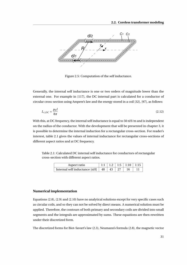
2.2. Coreless transformer modeling
dl1
xy
C1 C2dl2
R
Figure 2.5: Computation of the self inductance.
Generally, the internal self inductance is one or two orders of magnitude lower than the
external one. For example in [117], the DC internal part is calculated for a conductor of
circular cross-section using Ampere’s law and the energy stored in a coil [32], [97], as follows:
Li ,DC = µ0l
8π(2.12)
With this, at DC frequency, the internal self inductance is equal to 50 nH/m and is independent
on the radius of the conductor. With the development that will be presented in chapter 3, it
is possible to determine the internal induction for a rectangular cross-section. For reader’s
interest, table 2.1 gives the values of internal inductance for rectangular cross-sections of
different aspect ratios and at DC frequency.
Table 2.1: Calculated DC internal self inductance for conductors of rectangularcross-section with different aspect ratios.
Aspect ratio 1:1 1.2 1:5 1:10 1:15Internal self inductance [nH] 48 43 27 16 11
Numerical implementation
Equations (2.8), (2.9) and (2.10) have no analytical solutions except for very specific cases such
as circular coils, and so they can not be solved by direct means. A numerical solution must be
applied. Therefore, the contours of both primary and secondary coils are divided into small
segments and the integrals are approximated by sums. These equations are then rewritten
under their discretized form.
The discretized forms for Biot-Savart’s law (2.3), Neumann’s formula (2.8), the magnetic vector
31

Chapter 2. Coreless transformer modeling
potential (2.9) and (2.10) are respectively given by:
B = µ0I
4π
∑C1
∆l1 ×R
R3 (2.13)
L12 = µ0
4π
∑C2
∑C1
∆l2 ·∆l1
R(2.14)
A = µ0I1
4π
∑C1
∆l1
R(2.15)
L12 = 1
I1
∑C2
A ·∆l2 (2.16)
Here, the infinitesimal vectors dl1 and dl2 from integral formulations become respectively
the vectors ∆l1 and ∆l2 whose discretization length, also called step size, has to be judiciously
chosen.
Indeed, the crucial point concerning the discretized model is to set the correct step size. There
is a trade-off between the computation time and the resulting accuracy. In [117], experimental
rules are defined in order to choose the largest step size providing a solution with an acceptable
error. Nevertheless, the impact of the step size on the obtained results is more deeply analyzed
in section 2.2.5.
2.2.4 Coupling factor and quality factor
Two more parameters are often used to describe coreless transformers. The first one is the
coupling factor that can be expressed as follows:
k = L12pL1L2
(2.17)
where L12 is the mutual inductance between the primary and secondary coils, L1, and L2 are
their respective self inductances. In conventional transformers, this value is close to 1, but
for coreless transformers a coupling factor around 0.5 (when the coils are well aligned) is very
32

2.2. Coreless transformer modeling
good, and for applications involving a large air gap, its value is often below 0.1.
The second one is the quality factor of a coils:
Q = ωL1
R1(2.18)
where ω is the pulsation associated to the operating frequency. This factor is an image of the
quality of a given coil. It defines its capacity to generate a large magnetic field and low losses.
According to [18], a quality factor below 10 represents a really poor coil that should be avoided
for CET, and values around 100 are excellent for industrial applications.
2.2.5 Validation and measurements
In order to validate the modeling of coreless transformers, a series of verifications are under-
taken. Therefore multiple experimental coils are used for measurements and comparisons
with the modeling. Before entering these considerations, it is necessary to define the main
parameters that are involved in coreless transformers so as to be able to describe correctly the
geometry of experimental coils.
To validate the modeling of the coreless transformers, two coils shapes (rectangular and
hexagonal) and two types of wires (Litz wires and PCB tracks) are considered. Furthermore,
their size is chosen in order to cover a large range of possible solutions.
Geometric parameters
The coils have different geometric parameters depending on whether they are rectangular
or hexagonal and whether they are made of PCB tracks or Litw wires. These differences
are shown in Fig. 2.6, and the parameters involved in coreless transformers are defined in
Table 2.2. Except for g , indices 1 or 2 can be attached to all parameters. They represent
respectively the primary and the secondary coil. Besides those parameters could be also
added the misalignment of the secondary coil compared to the primary one. Assuming the
coils are parallel to the (x, y) plane, the misalignment is defined by the displacements xd and
yd . As a result they are zero when the centers of the coils are superimposed.
Experimental coils
The characteristics of the experimental coils used in the following sections are presented in
Table 2.3. The two first proposed coils are rectangular shaped, made of Litz wires and their
size is rather large compared to the others. In fact, they are respectively the primary and the
33
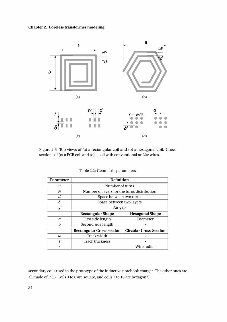
Chapter 2. Coreless transformer modeling
w
d
b
aw
d
a
(a) (b)
w dt
dd
r = w/2d
dd
(c) (d)
Figure 2.6: Top views of (a) a rectangular coil and (b) a hexagonal coil. Cross-sections of (c) a PCB coil and (d) a coil with conventional or Litz wires.
Table 2.2: Geometric parameters
Parameter Definition
n Number of turnsN Number of layers for the turns distributiond Space between two turnsδ Space between two layersg Air gap
Rectangular Shape Hexagonal Shapea First side length Diameterb Second side length -
Rectangular Cross-section Circular Cross-Sectionw Track width -t Track thickness -r - Wire radius
secondary coils used in the prototype of the inductive notebook charger. The other ones are
all made of PCB. Coils 3 to 6 are square, and coils 7 to 10 are hexagonal.
34

2.2. Coreless transformer modeling
Table 2.3: Characteristics of the experimental coils
Type n N a [mm] b [mm] w [mm] t [µm] r [mm] d [mm] δ [mm]1 Litz 1 1 220 140 - - 1.0 - -2 Litz 10 3 220 140 - - 1.0 0 03 PCB 16 1 50 50 1.0 105 - 0.5 -4 PCB 28 2 30 30 0.5 105 - 0.5 0.65 PCB 18 2 40 40 1.5 105 - 0.5 0.26 PCB 20 2 40 40 1.0 105 - 0.5 0.27 PCB 10 1 34.64 - 0.2 35 - 0.8 -8 PCB 10 1 34.64 - 0.9 35 - 0.1 -9 PCB 5 1 50 - 1.5 105 - 0.5 -
10 PCB 15 1 50 - 0.5 105 - 0.5 -
Magnetic flux density validation
The computed magnetic flux density (2.3) is verified by comparing it with results obtained
from magneto-static FEM simulations. Assuming the coils parallel to the (x, y) plane, only the
z-component of the magnetic flux density is evaluated. Its distribution is compared using coil
5 for two different heights.
First, the distribution of the magnetic flux density computed with (2.3) at a height of z = 5 mm
over the coil 5 when it is excited by a current of 1 A is shown in Fig. 2.7(a). It is compared to
FEM simulation in Fig. 2.7(b). The results show a good agreement since the relative difference
between computed and simulated values remains below 2 %. The maximal difference is
obtained in the center of the coil, where the intensity of the magnetic flux density is the
highest.
Then, a second comparison is made with the same conditions but at a height of z = 1 mm over
the coil 5. The results computed with (2.3) and simulated are respectively given in Fig. 2.7(c)
and (d). The relative difference remains below 9 %, and the maximal values are obtained at the
corners of the most internal turns. This difference can be explained by the very short distance
of evaluation and by the approximation of (2.3), where the wires are considered as infinitely
thin filaments. So all the current is concentrated in these filaments, and this results in a larger
magnetic field intensity just over them, especially when the distance of evaluation is short.
Inductances: step size definition
In order to find the good compromise between accuracy and time computation, the step
size for the numerical implementation of inductances presented in section 2.2.3 is analyzed
through two sets of computations.
35
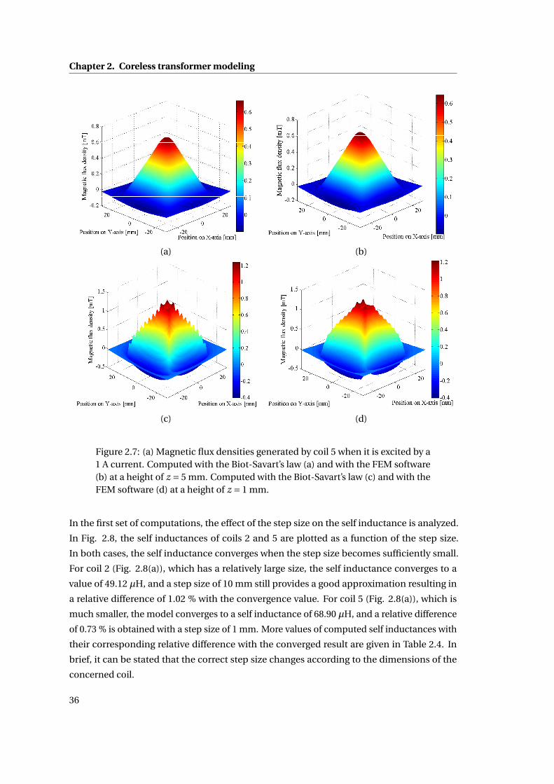
Chapter 2. Coreless transformer modeling
(a) (b)
(c) (d)
Figure 2.7: (a) Magnetic flux densities generated by coil 5 when it is excited by a1 A current. Computed with the Biot-Savart’s law (a) and with the FEM software(b) at a height of z = 5 mm. Computed with the Biot-Savart’s law (c) and with theFEM software (d) at a height of z = 1 mm.
In the first set of computations, the effect of the step size on the self inductance is analyzed.
In Fig. 2.8, the self inductances of coils 2 and 5 are plotted as a function of the step size.
In both cases, the self inductance converges when the step size becomes sufficiently small.
For coil 2 (Fig. 2.8(a)), which has a relatively large size, the self inductance converges to a
value of 49.12 µH, and a step size of 10 mm still provides a good approximation resulting in
a relative difference of 1.02 % with the convergence value. For coil 5 (Fig. 2.8(a)), which is
much smaller, the model converges to a self inductance of 68.90 µH, and a relative difference
of 0.73 % is obtained with a step size of 1 mm. More values of computed self inductances with
their corresponding relative difference with the converged result are given in Table 2.4. In
brief, it can be stated that the correct step size changes according to the dimensions of the
concerned coil.
36

2.2. Coreless transformer modeling
10−4
10−3
10−2
10−1
35
40
45
50
Step size [mm]
Sel
f ind
ucta
nce
[µH]
10−4
10−3
10−2
3
3.5
4
4.5
5
5.5
6
6.5
7
Step size [mm]
Sel
f ind
ucta
nce
[µH]
(a) (b)
Figure 2.8: Self inductance computed as a function of the step size for coil 2 (a)and for coil 5 (b).
Table 2.4: Self inductance computations as a function of the step size.
Step size [mm] 0.1 0.5 1.0 2.0 5.0 10.0 20.0 50.0
Coil 2
Computed selfinductance [µH]
49.1 49.1 49.0 49.0 48.9 48.6 46.4 43.4
Relative differ-ence [%]
0 0 0.20 0.20 0.41 1.02 5.50 11.61
Coil 5
Computed selfinductance [µH]
68.9 68.4 68.4 65.6 63.3 53.7 33.4 -
Relative differ-ence [%]
0 0.73 0.73 4.79 8.13 22.06 51.52 -
In the second set of computations, the effect of the step size on the mutual inductance is
analyzed. Fig. 2.9(a) shows the mutual inductances between coils 1 and 2 as a function of the
air gap. They are computed using Stokes’ theorem (2.5) and Neumann’s formula (2.14). The
former is solved using directly the function dblquad from the MATLAB toolbox, and the later
is solved with different step sizes. The results show that both approaches provide equivalent
results for small step sizes. More specifically, for step sizes smaller or equal to 10 mm, the
relative difference using Stokes’ theorem is much smaller than 1 %.
Fig. 2.9(b)) shows the mutual inductances between coils 5 and 6 as a function of a lateral
displacement xd . Only a positive displacement along the X axis is considered for symmetry
reasons. The results show that Stokes’ theorem and Neumann’s formula with a step size of
1 mm provide equivalent results with a relative difference much smaller than 1 %. For a step
size of 10 mm, the difference becomes more noticeable, that is about 13.7 % when xd is equal
37

Chapter 2. Coreless transformer modeling
to zero, but it decreases when xd becomes larger.
It is also interesting to compare the computation time between Stokes’ and Neumann’s ap-
proaches and for different step sizes. The goal is to obtain accurate values (with a relative
difference smaller than 1 %) in the shortest computation time. The interest comes from that it
allows to gain a considerable time in an optimization process that may require more than 105
inductances computations (see chapter 4). In Fig. 2.9(b), nine different positions are evaluated
for the mutual inductance computations. The computation time is compared in Table 2.5 for
both approaches and for different step sizes. Hence, the discretized model is really interesting,
even for small step sizes, because it provides accurate and quick results.
0 20 40 60 80 1000
0.5
1
1.5
2
2.5
3
3.5
4
Air gap [mm]
Mut
ual i
nduc
tanc
e [µ
H]
Stoke’s theoremNeum. step size = 1 [mm]Neum. step size = 10 [mm]Neum. step size = 30 [mm]Neum. step size = 50 [mm]
0 5 10 15 20 25 30 35 40
0
1
2
3
4
5
Displacement along X axis [mm]
Mut
ual i
nduc
tanc
e [µ
H]
Stoke’s theoremNeum. step size = 1 [mm]Neum. step size = 3 [mm]Neum. step size = 5 [mm]Neum. step size = 10 [mm]Neum. step size = 20 [mm]
(a) (b)
Figure 2.9: (a) Mutual inductance computation between coils 1 and 2. (b) Mutualinductance computation between coils 5 and 6.
Table 2.5: Computation time for different cases issued from Fig. 2.9(b).
Neumann’s formulaStep size = 10 mm
Neumann’s formulaStep size = 1 mm
Neumann’s formulaStep size = 0.1 mm
Stokes’ theorem
~ 1 s 5 s 43 s 278 s
As a conclusion, it can be stated that the dimensions of the coils have a major impact on the
choice of the step size which must be fixed accordingly. For the mutual inductance, the larger
the distance between the coils (lateral or vertical), the lower is the impact of the step size.
However, the step size is more critical for the self inductance computation, as seen through
the two sets of computations. As a global rule, we consider the results of an inductance
computation as accurate enough when the step size does not cause an error greater than 1 %
in comparison with its value of convergence. In all cases encountered in this work, a step size
of 0.5 mm for the mutual inductances and a step size of 0.1 mm for the self inductances fulfil
38

2.2. Coreless transformer modeling
by far this condition while considering coils with an external size greater or equal to 20 mm.
Thereby, those step sizes are used by default in this thesis or it is mentioned otherwise.
Inductance measurements
The inductances are measured with a HP Precision LCR Meter 4284A (20Hz-1MHz) at 200 kHz.
Litz wires are used as connection cables from the coils to the LCR Meter, and they are reduced
to their shortest length so as to minimize their effect on the measurement. Generally, their
contribution to the total inductance is insignificant, as their length is much shorter than the
one of the coil track. But in the following measurements, they are taken into account. The
inductance of connection cables is evaluated by measuring it on a twisted pair of straight
Litz wires of 1 mm radius, resulting in a linear inductance of 0.6 µH/m. For instance, the
contribution of the connection cables for coils 3 to 6 is much smaller than 1 % of the total self
inductance and can be therefore neglected. This is due to the high number of turns which
ensures a long length of track. For coils 1 and 2, the inductance of the connection cables
corresponds respectively to 12.9 % and 0.4 % of the total inductance. Because the coil 1 has
only a single turn, the length of the connection cables are significant compared to the length
of the coil itself, and as a result, their effect on the total inductance cannot be neglected.
In Table 2.6, the measured self inductances of coils 1 to 10 are compared with the computed
ones. For the measurements, the inductance of the connection cables is subtracted. The
relative error between measurements and computations with Neumann’s formula is also
provided. Measured and computed results are in good agreement as relative errors remain
smaller than 6 %.
Table 2.6: Results of the self inductance computations and measurements
Coil # Stoke Neumann Measurement Error1 806 nH 791 nH 821 nH 3.65 %2 49.12 µH 49.11 µH 52.20 µH 5.73 %3 5.97 µH 5.97 µH 5.85 µH 2.05 %4 11.18 µH 11.15 µH 11.35 µH 1.76 %5 6.91 µH 6.89 µH 7.12 µH 3.23 %6 11.44 µH 11.43 µH 11.50 µH 0.61 %7 2.49 µH 2.48 µH 2.43 µH 2.06 %8 2.27 µH 2.25 µH 2.35 µH 4.26 %9 1.22 µH 1.22 µH 1.28 µH 4.69 %
10 7.12 µH 7.10 µH 7.24 µH 1.93 %
The method used to measure mutual inductances is as follows. First of all, the coils are set
in the position for which the mutual inductance is wanted to be measured. Two successive
39
Chapter 2. Coreless transformer modeling
measurements are then required. First, both coils are connected in series, and the inductance
L A thus obtained is defined as:
L A = L1 +L2 +2L12 (2.19)
where L1, L2 are the self inductances of the coils and L12 is the mutual inductance. Secondly,
the terminals of one of the coil are inverted, which gives the inductance LB defined as:
LB = L1 +L2 −2L12 (2.20)
The mutual inductance is then deduced by:
L12 = 1
4(L A −LB ) (2.21)
The mutual inductance can be deduced only from (2.19) if the self inductance of both coils is
known. However, performing the second measurement provides more accurate results as the
error due to the connection cables is automatically compensated in the subtraction of (2.21).
In Table 2.7, the measured mutual inductances between different couples of coils 1 to 6 are
compared with computed ones. The relative error is given between the results computed
with the Neumann’s formula and the measurements. They are in good agreement with errors
remaining below 5 %.
Table 2.7: Results of the mutual inductance computations and measurements.
Coupled coils Airgap Stoke Neumann Measurement Error1-2 15 mm 2.51 µH 2.48 µH 2.58 µH 3.88 %1-2 30 mm 1.63 µH 1.62 µH 1.69 µH 4.14 %3-4 2.5 mm 4.72 µH 4.71 µH 4.80 µH 1.88 %3-4 5 mm 3.66 µH 3.65 µH 3.78 µH 3.44 %5-6 5 mm 5.11 µH 5.11 µH 4.91 µH 4.07 %
Finally, in Fig. 2.10, the mutual inductance between coils 1 and 2 is measured when the air
gap is varied, and the mutual inductance between coils 5 and 6 is measured when the lateral
displacement is varied, as for Fig. 2.9. In both cases the relative error between measured and
computed values remains smaller than 8 %.
2.3 Equivalent electric circuit modeling
The goal of this section consists in calculating the electric parameters of the transformer once
the inductances and the resistances are known. It is possible to determine the voltages and
40

2.3. Equivalent electric circuit modeling
0 20 40 60 80 1000
0.5
1
1.5
2
2.5
3
3.5
4
Air gap [mm]
Mut
ual i
nduc
tanc
e [µ
H]
MeasurementNeum. step size = 0.1 [mm]
0 5 10 15 20 25 30 35 40−1
0
1
2
3
4
5
6
Displacement along X axis [mm]
Mut
ual i
nduc
tanc
e [µH
]
MeasurementNeum. step size = 0.1 [mm]
(a) (b)
Figure 2.10: (a) Measured and computed mutual inductance between coils 1 and2. (b) Measured and computed mutual inductance between coils 5 and 6.
currents in the primary and secondary sides with the voltage equations of the transformer, and
consequently the power generated by the source or consumed by the load. In the second part
of this section, the choice of the compensation capacitors and their evaluation are discussed.
The main electric parameters of coreless transformers are listed in Table 2.8.
Table 2.8: Electric parameters.
Parameter Definition
L1 Primary inductanceL2 Secondary inductanceL12 Mutual inductanceR1 Primary resistanceR2 Secondary resistanceRL Load resistanceC1 Primary compensation capacitorC2 Secondary compensation capacitorI1 RMS source current
IL1 RMS current in the primary coilI2 RMS load current
IL2 RMS current in the secondary coilω Electric pulsation
41

Chapter 2. Coreless transformer modeling
2.3.1 General electric circuit
Let us consider the electric circuit in the simplest case, i.e. when no compensation capacitors
are present. This circuit is shown in Fig. 2.11. The approach to solve the coreless transformer
circuit is similar to the one proposed in [38], [37], [90], but is adapted and treated more in
detail. The system is assumed to be excited by a perfect sine wave in a steady state condition.
U1
R1 L1 L2 R2
RL
IL2IL1
-jωL12IL2 jωL12IL1
U1
R1 L1
Z2
IL2IL1
-jωL12IL2 jωL12IL1
U1
R1 L1
IL1
ZR
U1
IL1
Zeq
Figure 2.11: Electric circuit of the coreless transformer.
In this section, a distinction is made between the current delivered by the source I 1 and
the current flowing in the primary coil I L1. Similarly for the secondary side, a distinction is
made between the current in the load I 1 and the current in the secondary coil I L1. However,
when there are no compensation capacitors or when they are placed in series with the self
inductances, those currents are respectively equal (i.e. I 1 = I L1 and I 2 = I L2). This can be
observed in Fig. 2.13.
As a result, when there are no compensation capacitors, the primary and secondary voltage
equations are respectively given by:
U 1 = R1I L1 + jωL1I L1 − jωL12I L2 (2.22)
and
U 2 = jωL12I L1 = (R2 +RL)I L2 + jωL2I L2 (2.23)
Here, the first equality of the second voltage equation is not so trivial. It provides the basic
information on how inductive coupling works and governs the condition that allows to obtain
higher voltage levels at the secondary. Indeed, the voltage induced in the secondary coil is
proportional to the frequency, the mutual inductance and the current of the primary coil. If
the transferred power is wanted to be increased for a given application, at least one of these
three parameters has to be increased.
42

2.3. Equivalent electric circuit modeling
An usual way to solve the circuit consists in analyzing the effect of the complete secondary
circuit on the primary side. Basically, the secondary circuit is viewed from the primary voltage
supply as an impedance, namely the reflected impedance Z R which is highly dependent on
the geometric configuration of the primary and secondary coils. The electric circuit of the
coreless transformer can be fully determined in four steps, as shown in Figs. 2.11 and 2.12.
1. Step 1: The electric circuit of the coreless transformer is given in Fig. 2.11. The unknown
variables are the current in the primary coil IL1 and the current in the secondary coil IL2;
2. Step 2: The secondary circuit is reduced to a single impedance Z 2 (Fig. 2.12(a));
3. Step 3: The whole secondary circuit is replaced by the reflected impedance Z R in the
primary (Fig. 2.12(b));
4. Step 4: Knowing the total equivalent impedance Z eq viewed from the voltage supply
(Fig. 2.12(c)), it is possible to determine IL1 and then to deduce IL2.
To determine the reflected impedance, it is convenient to write the secondary components as
a single impedance, that is the total secondary impedance Z 2 given by:
Z 2 = R2 +RL + jωL2 (2.24)
Then by substituting I L2 from (2.23), the term jωL12I L2 of (2.22) becomes:
jωL12I L2 =−ω2L2
12
Z 2I L1 =−Z R I L1 (2.25)
As a result, the reflected impedance can be expressed as follows:
Z R = (R2 +RL)ω2L212
(R2 +RL)2 +ω2L22
− jω3L2
12L2
(R2 +RL)2 +ω2L22
(2.26)
where the first term is respectively the real part and the second term the imaginary part of the
reflected impedance. With this, (2.22) becomes:
U 1 = (R1 + jωL1 +Z R )I L1 = Z eq I L1 (2.27)
with Zeq the total impedance seen by the voltage supply. It is determined by combining the
primary and secondary circuits. Assuming that the sinusoidal voltage amplitude of the supply
U 1 is known, (2.27) allows to calculate the current I L1 that flows in the primary coil. The power
P12 transferred from the primary coil to the secondary is given by the real part of the reflected
43

Chapter 2. Coreless transformer modeling
U1
R1 L1 L2 R2
RL
IL2IL1
-jωL12IL2 jωL12IL1
U1
R1 L1
Z2
IL2IL1
-jωL12IL2 jωL12IL1
U1
R1 L1
IL1
ZR
U1
IL1
Zeq
(a)
U1
R1 L1 L2 R2
RL
I2IL1
-jωL12IL2 jωL12IL1
U1
R1 L1
Z2
I2IL1
-jωL12IL2 jωL12IL1
U1
R1 L1
IL1
ZR
U1
IL1
Zeq
U1
R1 L1 L2 R2
RL
I2IL1
-jωL12IL2 jωL12IL1
U1
R1 L1
Z2
I2IL1
-jωL12IL2 jωL12IL1
U1
R1 L1
IL1
ZR
U1
IL1
Zeq
(b) (c)
Figure 2.12: (a) Step 2: Simplification of the secondary circuit. (b) Step 3: Reflectedimpedance of the secondary circuit. (c) Step 4: Total equivalent impedance of thecoreless transformer.
impedance multiplied by the square of the primary current magnitude as follows:
P12 =ℜZ R I 2L1 (2.28)
Assuming that the input voltage U 1 is perfectly sinusoidal, the difference between the input
power Pi n delivered by the voltage supply and the transferred power P12 corresponds to
the Joule losses in the resistance of the primary coil. Furthermore, the power transferred to
the load is defined as the load resistance multiplied by the square of the secondary current
amplitude:
PL = RL I 2L2 (2.29)
Similarly, the difference between the transferred power P12 and the load power PL is due to
the Joule losses in the resistance of the secondary coil. So basically, considering the simple
44

2.3. Equivalent electric circuit modeling
coreless transformer presented in this subsection, three issues can be stated:
1. The losses in coreless transformers are caused only by the Joule effects in respectively
the primary and secondary coils. Therefore, these resistances are wanted to be as small
as possible. In the same time, the self-inductances of the coils have to be maximized,
since they represent their ability to generate a magnetic flux density for a given current.
Generally, a high inductance goes with a high resistance, so there is a trade-off with an
optimal solution for every application which has to be investigated. The goal is then to
use coils with the highest possible quality factor.
2. For a coreless transformer without secondary resonant capacitors the power transferred
to the load can not be sufficient unless the input voltage is large. The reason is that the
secondary coil impedance R2 + jωL2 is generally great and therefore is responsible for a
significant current drop in the load resistance. The simplest way to circumvent this issue
is to increase the input voltage so that the power transferred to the load is sufficient. But
this solution is not optimal because it requires higher current amplitudes in the primary
coil, which in turn generates greater Joule losses. This may lead to dramatic results in
terms of efficiency and Joule losses.
3. The previous point leads to the necessary addition of resonance capacitors to the pri-
mary and secondary circuits. By decreasing or even cancelling the large reactance of
a coil, the resonance capacitors allow to reduce the current amplitudes and therefore
to improve the efficiency of coreless transformers, and the optimum is reached at the
resonance frequency. Resonant circuits are widely used to enhance inductive power
transmission. They involve an alternating exchange of energy between the capacitor and
the inductance of the coil, and the amount of energy required to maintain the oscillation
is minimal. To understand this effect, it can be compared to the movement of a swing,
where the energy of each push is added to the total energy if applied at the right time.
There are many different possible configurations for the capacitors, as discussed in the
following subsection. They have also an impact on the equations presented above.
2.3.2 The four topologies
In addition to the case where they are not present, the resonance capacitors can be placed
in parallel or in series with the inductance of the coil. In the scope of this thesis, only the
cases when they are present are considered of interest. This gives four different possible
configurations. In the following, the letter S stands for a capacitor in series with the coil and
P for a capacitor in parallel. The four topologies shown in 2.13 are labelled as SS, PS, SP and
PP, where the first letter identifies the primary capacitor and the second one identifies the
45

Chapter 2. Coreless transformer modeling
secondary capacitor.
Each different topology has its advantages and drawbacks. The choice has to be made ac-
cording to the specifications of the application to develop. In [120], [125], [126], [127], these
advantages and drawbacks are discussed more in detail. However, the different topologies are
discussed without taking into account the resistances of the coils because they are assumed to
be insignificant.
Therefore, in the following points, each topology is briefly discussed. The addition of the
capacitors modifies the equations presented in the previous section. The new formulations
for the different topologies are presented and the resistances of the coils are also included in
the model.
R1C1
L1 L2
R2C2
R1
L1C1 L2
R2C2 R1
L1C1 L2
R2
C2
L2
R2
C2
R1C1
L1
SS SP
PS PP
IL1 IL2 IL1 IL2 I2
I1 IL1 IL2 IL2 I2I1 IL1
R1C1
L1 L2
R2C2
R1
L1C1 L2
R2C2 R1
L1C1 L2
R2
C2
L2
R2
C2
R1C1
L1
SS SP
PS PP
IL1 IL2 IL1 IL2 I2
I1 IL1 IL2 IL2 I2I1 IL1
(a) (b)
R1C1
L1 L2
R2C2
R1
L1C1 L2
R2C2 R1
L1C1 L2
R2
C2
L2
R2
C2
R1C1
L1
SS SP
PS PP
IL1 IL2 IL1 IL2 I2
I1 IL1 IL2 IL2 I2I1 IL1
R1C1
L1 L2
R2C2
R1
L1C1 L2
R2C2 R1
L1C1 L2
R2
C2
L2
R2
C2
R1C1
L1
SS SP
PS PP
IL1 IL2 IL1 IL2 I2
I1 IL1 IL2 IL2 I2I1 IL1
(c) (d)
Figure 2.13: (a) Series-Series (SS) topology. (b) Parallel-Series (PS) topology. (c)Series-Parallel (SP) topology. (d) Parallel-Parallel (PP) topology.
Series compensated secondary
With the addition of a series capacitor, the secondary impedance (2.24) and the reflected
impedance (2.26) can be rewritten as follows:
Z 2 = R2 +RL + jωL2 − j1
ωC2(2.30)
46

2.3. Equivalent electric circuit modeling
and
Z R = ω4C 22 L2
12(R2 +RL)
(ω2C2L2 −1)2 +ω2C 22 (R2 +RL)2
− jω3C2L2
12(ω2C2L2 −1)
(ω2C2L2 −1)2 +ω2C 22 (R2 +RL)2
(2.31)
To obtain the maximal power transferred from the primary to the secondary of (2.28), the goal
is to maximize the real part of the reflected impedance and to cancel the imaginary part. By
working at the resonance frequency, an advantage of a series compensation capacitor is that
the secondary impedance and therefore the reflected impedance are purely resistive. So there
is no reflected reactance generating additional losses. The secondary resonance frequency is
given by:
ω0 = 1pL2C2
(2.32)
At the resonance frequency, the total secondary impedance Z 2 becomes:
Z 2 = R2 +RL + j (ω0L2 − 1
ω0C2) = R2 +RL (2.33)
As a result, the reflected impedance is given by:
Z R = ω20L2
12
R2 +RL(2.34)
which is purely resistive. This shows with (2.28) that a series compensated secondary behaves
like a voltage source and is well suited to supply a stable load voltage when the coreless trans-
former is supplied by a current source. This statement is verified through a set of calculations
in appendix A.
Another advantage of the secondary compensated capacitor is that the resonant frequency
is independent on the mutual inductance, which is interesting for applications where the
secondary coil position is expected to be variable.
Parallel compensated secondary
With the addition of a parallel capacitor, the secondary and reflected impedances are respec-
tively given by:
Z 2 = R2 + jωL2 + 11
RL+ jωC2
(2.35)
47

Chapter 2. Coreless transformer modeling
and
Z R = ω2L212(1+ω2L2
2R2L)(R2 +RL +ω2L2C2RL)
(R2 +RL +ω2L2C2RL)2 + (ωL2 −ωC2RLR2 −ωC2R2L)2
− jω2L2
12(1+ω2L22R2
L)(ωL2 −ωC2RLR2 −ωC2R2L)
(R2 +RL +ω2L2C2RL)2 + (ωL2 −ωC2RLR2 −ωC2R2L)2
(2.36)
Here, just to simplify the expression and to highlight the impact of the parallel compensated
capacitor, the resistance of the secondary is neglected, keeping in mind that it is not the case
in the model. At the resonant frequency, the reflected impedance is then reduced to:
Z R = L212RL
L22
− jω0L2
12
L2(2.37)
Thereby, the reflected impedance has a capacitive reactance when the secondary capacitor
is in parallel. Of course, this reactance can be also compensated by the primary inductance
together with the primary capacitor.
Given that the coreless transformer is supplied by a current source, (2.28) with (2.37) show that
a parallel compensated secondary behaves like a current source and is is well suited to supply
a stable secondary load current. This statement can be verified through a set of computations
given in appendix A.
Series compensated primary
A series compensated primary can be used to cancel the inductance of the coil at resonance
frequency. This allows to reduce the voltage of the source to manageable levels. The total
impedance Z eq seen by the voltage supply is given by:
Z eq = R1 + jωL1 + 1
jωC1+Z R , (2.38)
where the imaginary part is cancelled at resonance frequency. A great advantage of this primary
topology is that the reactive impedance compensation of the primary coil is independent on
the mutual inductance and the load resistance. To perform this, the capacitor has to be simply
designed so that it exactly cancels the impedance of the primary inductance:
C1 = 1
ω20L1
. (2.39)
However, this topology has also two disadvantages. First, when the load becomes small or
48

2.3. Equivalent electric circuit modeling
when the mutual inductance becomes weak (which happens when the secondary coil is
removed from the CET system for example), the primary circuit will draw very large currents
from the source. This is due to the decrease of the reflected impedance and to the fact that the
primary inductance is cancelled by the primary capacitor. To solve this problem, a current
limitation has to be implemented.
Secondly, if the load increases (that is the load resistance decreases) or if the mutual induc-
tance increases (that is when the primary and secondary coils are well aligned), the reflected
impedance will greatly increase, which in turn will cause the primary current to decrease and
thus result in a smaller power transferred to the load. This is unacceptable to ensure a minimal
voltage induced in the load. To solve this problem, a primary current regulation should be
implemented.
Parallel compensated primary
A parallel capacitor is generally used to generate large currents in the primary coil, which
in return may require a large voltage supply because of the intrinsic large impedance of the
primary coil at high frequency. The total impedance Z eq seen by the voltage supply is given
by:
Z eq = 1
jωC1 + 1R1+ jωL1+Z R
(2.40)
In this configuration, the interesting point is that the voltage applied to the primary coil is
also the voltage applied to the capacitor. At resonance frequency, the current and the voltage
delivered by the sinusoidal voltage supply should have a zero phase angle. This way they are
exactly in phase and no reactive loss is generated.
The strategy to design the primary capacitor consists in considering the total circuit without
the capacitor itself and to write its corresponding impedance as follows:
Z t = R1 + jωL1 +Z R = Rt + j X t (2.41)
where Z t is the total impedance seen by the voltage source without the primary capacitor,
Rt and X t are respectively the real part and the imaginary part of this impedance. The total
impedance in (2.40) can then be rewritten as follows:
Z eq = Rt
(1−ωC1X t )2 +ω2C 21 R2
t
+ jX t −ωC1R2
t −ωC1X 2t
(1−ωC1X t )2 +ω2C 21 R2
t
(2.42)
Here, the condition of zero phase angle is reached only if Z eq is purely resistive. Therefore the
49

Chapter 2. Coreless transformer modeling
primary capacitor has to be designed so that the imaginary part of (2.42) is cancelled. This is
achieved with:
C1 = X t
ω(R2t +X 2
t )(2.43)
For example, in the specific case of a series compensation of the secondary coil and at the
resonance frequency, the primary capacitor takes the following form:
C1 = L1(R2 +RL)2
ω40L4
12 +ω20(2R1L2
12(R2 +RL)+L21(R2 +RL)2)+R2
1(R2 +RL)2(2.44)
A similar development can be made for a parallel compensated secondary. The main drawback
of a parallel compensation at the primary is that the compensation of the reactive part of
the whole circuit is a function of the mutual inductance and the load. However, the reflected
impedance is generally much smaller than the primary coil impedance and therefore the
impact of its variation is not critical for the primary capacitor design.
2.3.3 Discussion
In this section, the equivalent electric circuit of the coreless transformer has been presented.
The different topologies with or without compensation capacitors have been analyzed through
the general equations of transformers. The main contributions here are the integration of the
resistances in the model and the discussion on the advantages and drawbacks of the different
existing topologies.
2.4 Conclusion
In this chapter, different aspects of the coreless transformer have been addressed. First, the
analytical and numerical models for the inductances have been presented. The model has
then been validated through multiple sets of measurements. A special effort has been put
in determining the right compromise between the computation time and the accuracy in
anticipation of the forthcoming problem of optimization.
In the second part of this chapter, the equivalent electric circuit of the coreless transformer
has been thoroughly analyzed, allowing to highlight the advantages and drawbacks of the
different existing compensation topologies.
50

CHAPTER 3
High frequency effects
Summary3.1 Introduction . . . . . . . . . . . . . . . . . . . . . . . . . . . . . . . . . . . . . . 52
3.1.1 Definition of the skin and proximity effects . . . . . . . . . . . . . . . . . 52
3.1.2 Equivalent electric circuit of a coil . . . . . . . . . . . . . . . . . . . . . . 53
3.1.3 Joule losses and efficiency issues . . . . . . . . . . . . . . . . . . . . . . . 56
3.1.4 Problem definition . . . . . . . . . . . . . . . . . . . . . . . . . . . . . . . 56
3.2 First numerical method . . . . . . . . . . . . . . . . . . . . . . . . . . . . . . . 59
3.2.1 Current density modeling . . . . . . . . . . . . . . . . . . . . . . . . . . . 59
3.2.2 Resistance calculation . . . . . . . . . . . . . . . . . . . . . . . . . . . . . 61
3.2.3 Internal self inductance calculation . . . . . . . . . . . . . . . . . . . . . 62
3.2.4 Validation and measurements . . . . . . . . . . . . . . . . . . . . . . . . 63
3.3 Numerical modeling using FEM . . . . . . . . . . . . . . . . . . . . . . . . . . 65
3.3.1 Introduction . . . . . . . . . . . . . . . . . . . . . . . . . . . . . . . . . . . 65
3.3.2 Geometrical structure and model of a coil . . . . . . . . . . . . . . . . . 65
3.3.3 Meshing of the conductors . . . . . . . . . . . . . . . . . . . . . . . . . . 67
3.3.4 Physical and electrical definition . . . . . . . . . . . . . . . . . . . . . . . 68
3.3.5 Validation and measurements . . . . . . . . . . . . . . . . . . . . . . . . 70
3.4 Discussion . . . . . . . . . . . . . . . . . . . . . . . . . . . . . . . . . . . . . . . 70
3.5 Exploitation of FEM simulations . . . . . . . . . . . . . . . . . . . . . . . . . . 72
3.5.1 Design of experiments . . . . . . . . . . . . . . . . . . . . . . . . . . . . . 72
3.5.2 Complete output mapping . . . . . . . . . . . . . . . . . . . . . . . . . . 74
3.6 Effective impact of the high frequency on CET . . . . . . . . . . . . . . . . . . 76
3.7 Overall conclusion . . . . . . . . . . . . . . . . . . . . . . . . . . . . . . . . . . 77

Chapter 3. High frequency effects
This chapter addresses the high frequency (HF) effects in the coils. Two different methods are
investigated. The first one is based on the resolution of Maxwell’s equations. The second one
uses FEM simulations. A strategy to exploit effectively the results is then developed. Finally,
the main repercussions of HF effects on coreless transformers are analyzed in terms of losses
and efficiency.
3.1 Introduction
3.1.1 Definition of the skin and proximity effects
Working at high frequency gives rise to effects that alter the behavior of electric currents in
conductors. A time-varying current flowing inside a conductor generates a magnetic field that
interacts with the current itself. More specifically, the varying magnetic field induces currents
that oppose the one generated by the external source at the center of the cross-section, and
that strengthen it at the periphery.
If a single conductor is involved, this results in a current accumulation at its periphery, and
the higher is the operating frequency, the greater becomes this accumulation. This is referred
to as the skin effect. For multiple close conductors, the current undergoes interactions from
one conductor to another, and the current also tends to accumulate at their periphery. This
is referred to as the proximity effect. Both skin and proximity effects are caused by the same
physical phenomenon. They can be modeled in a similar way, and they define how the
resistance and the internal self inductance of a coil varies with the frequency. Many works in
literature have tried to define high frequency effects in conductors, and a short review of the
most interesting ones is proposed here.
For a single circular conductor, the skin effect can be easily expressed in an analytical form
with Bessel equations [54], [93], [118]. For multiple neighboring conductors, a numerical
solution is derived from 2D-FEM simulations in [117].
In [26], [66], the impedance of rectangular conductors is computed by dividing the cross-
section into several subbars, which allows to obtain a numerical solution for single and
multiple conductors.
Another interesting method for multiple conductors of rectangular cross-section is presented
in [44], [43], [42], based on the evaluation of the electric field and the current density on each
segment of the discretized perimeter cross-sections.
In [61], the skin and proximity effects are evaluated through 2D-FEM simulations. Corrective
52

3.1. Introduction
coefficients are derived and integrated to the impedance of the coil. These coefficients are
functions of the frequency, the geometry and the fill factor of the conductors.
Finally, The PEEC (Partial Element Equivalent Circuit) method can be used to extract the
electric parameters such as the resistance and the self inductance from the geometry of the
conductors. It is well adapted to model structures that contain different kinds of metallic
conductors. Multiple publications deal with the PEEC method [36], [47], and commercialized
softwares exist such as the InCa3D solver by Cedrat [22]. The main advantage of this solu-
tion compared to the FEM one is that only the conductors have to be meshed and not the
surrounding air, which allows to reduce the computation time.
3.1.2 Equivalent electric circuit of a coil
Formulations for DC resistance RDC and DC internal self inductance Li ,DC of coils are respec-
tively discussed in sections 2.2.1 and 2.2.3. However, CET is performed at high frequencies,
generally situated from 10 kHz to 5 MHz, which may induce changes in the magnitudes of
resistance and inductance. To differentiate them from the DC case, we speak of AC resistance
RAC and AC internal self inductance Li ,AC . Furthermore, the modeling of the inductor coil
proposed in Fig. 2.2 is no longer valid at high frequencies, as the parasitic capacitance may be
no more negligible.
The multiple parallel turns of the coil gives rise to an equivalent parasitic capacitance in
parallel to the resistance and inductance of the coil, as illustrated in Fig. 3.1. This parasitic
capacitance Cpar is relatively small (in the order of 10 pF) which makes it insignificant at low
frequencies but not at very high frequencies (> 5 MHz).
R
L
Cpar
Figure 3.1: Equivalent electric circuit of a coil at high frequency.
As a result, the impedance of a coil is defined as follows:
Z−1 = jωCpar + 1
R + jωL(3.1)
where R and L are respectively the resistance and the self inductance of the coil. This gives
53

Chapter 3. High frequency effects
respectively the following real and imaginary parts for the coil impedance:
ℜZ = R
(1−ω2LCpar )2 + (ωRCpar )2 (3.2)
ℑZ = ωL−ωR2C −ω3L2Cpar
(1−ω2LCpar )2 + (ωRCpar )2 (3.3)
For the modeling of the coreless transformers, it is not necessary to compute accurately the
parasitic capacitance, as its impedance is insignificant compared to the one of the other
components. For example, the measured parasitic capacitance of coil 5 (from Table 2.3) is
88 pF. This is a great value because of the large track width and the two copper layers. The
corresponding impedance of the parasitic capacitance is about 9 kΩ at 200 kHz and 0.9 kΩ at
2 MHz. It is much greater than the impedance of the self inductance that is 8.67Ω at 200 kHz
and 86.70Ω at 2 MHz. For comparison, the measured parasitic capacitance of coil 10 is 1.14 pF.
At 200 kHz, the impedance of its parasitic capacitance is about 70 kΩ and the impedance of its
self inductance is 8.92Ω, and at 2 MHz, they are respectively 7 kΩ and 89.22 Ω.
So the parasitic capacitance can be neglected for the modeling of the coreless transformer.
However, it may have an impact on the measurement of the resistance and the self inductance
of a coil and therefore has to be taken into account. The reason comes from that the parasitic
capacitance and the self inductance form a resonant circuit which leads to a huge increase of
impedance at resonance frequency. Fig. 3.2 shows a typical impedance variation of a coil with
hypothetical values of R = 1 Ω, L = 5 µH, Cpar = 10 pF. The self resonance frequency fs of a
coil can be calculated by:
fs = 1
2πp
LC(3.4)
This results for the values given above (corresponding to Fig. 3.2) to a self resonance frequency
of 22.50 MHz.
In practice, the resistance and self inductance of a coil cannot be measured by direct means
with a RLC meter at high frequency, because the resistance, the self inductance and the
parasitic capacitance cannot be physically dissociated. Instead, the real and imaginary parts of
its impedance Z are easily obtained. The self resonance frequency is determined by analyzing
the measured curves and the value of the parasitic capacitance can be derived from (3.4). The
effective measured resistance and self inductance are then obtained by resolving the system
of equations (3.2) and (3.3).
Furthermore, a few remarks concerning the operating frequency can be made. The operating
54
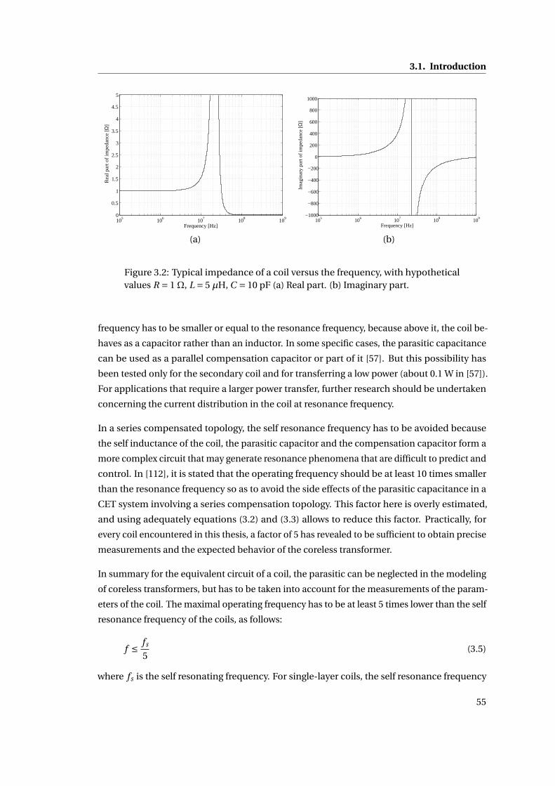
3.1. Introduction
105
106
107
108
109
0
0.5
1
1.5
2
2.5
3
3.5
4
4.5
5
Frequency [Hz]
Rea
l par
t of
impe
danc
e [Ω
]
105
106
107
108
109
−1000
−800
−600
−400
−200
0
200
400
600
800
1000
Frequency [Hz]
Imag
inar
y pa
rt o
f im
peda
nce
[Ω
]
(a) (b)
Figure 3.2: Typical impedance of a coil versus the frequency, with hypotheticalvalues R = 1Ω, L = 5 µH, C = 10 pF (a) Real part. (b) Imaginary part.
frequency has to be smaller or equal to the resonance frequency, because above it, the coil be-
haves as a capacitor rather than an inductor. In some specific cases, the parasitic capacitance
can be used as a parallel compensation capacitor or part of it [57]. But this possibility has
been tested only for the secondary coil and for transferring a low power (about 0.1 W in [57]).
For applications that require a larger power transfer, further research should be undertaken
concerning the current distribution in the coil at resonance frequency.
In a series compensated topology, the self resonance frequency has to be avoided because
the self inductance of the coil, the parasitic capacitor and the compensation capacitor form a
more complex circuit that may generate resonance phenomena that are difficult to predict and
control. In [112], it is stated that the operating frequency should be at least 10 times smaller
than the resonance frequency so as to avoid the side effects of the parasitic capacitance in a
CET system involving a series compensation topology. This factor here is overly estimated,
and using adequately equations (3.2) and (3.3) allows to reduce this factor. Practically, for
every coil encountered in this thesis, a factor of 5 has revealed to be sufficient to obtain precise
measurements and the expected behavior of the coreless transformer.
In summary for the equivalent circuit of a coil, the parasitic can be neglected in the modeling
of coreless transformers, but has to be taken into account for the measurements of the param-
eters of the coil. The maximal operating frequency has to be at least 5 times lower than the self
resonance frequency of the coils, as follows:
f ≤ fs
5(3.5)
where fs is the self resonating frequency. For single-layer coils, the self resonance frequency
55

Chapter 3. High frequency effects
is generally situated between 30 MHz and 100 MHz. Their maximal operating frequency is
then set to 5 MHz. However, for two-layers coils, the self resonating frequency can be situated
between 5 and 10 MHz. Therefore, the maximal frequency for two-layers coils is frequently set
to 1 or 2 MHz.
3.1.3 Joule losses and efficiency issues
Assuming there is no metallic material in vicinity, the only losses that are generated when a
current is flowing through a coil are the Joule losses. Considering the equivalent circuit of Fig.
3.1, the Joule losses P j are defined as:
P j =ℜZ I 2 (3.6)
where I is the amplitude of the current (AC rms) in the coil and Z the impedance of the coil.
Given that condition (3.5) is respected, the only source of Joule losses are the resistances of
the coils. Then, by considering only the losses in the coreless transformer (and not the ones
generated in electronic components), the efficiency is given by:
η= Pi n
Pout= Pi n
Pi n +Ploss= Pi n
Pi n +m∑
i=1P j ,i
(3.7)
where m is the number of coils in the coreless transformer and P j ,i their associated Joule
losses.
3.1.4 Problem definition
Most experts and designers of CET systems involving PCB coils (this is also valid for Litz coils)
agree that, below 200 kHz, high frequency effects can reasonably be neglected [50], [51]. But
the veracity of this statement cannot be proven for every case and the limits of its applicability
are fuzzy. Furthermore, over 200 kHz these effects can be no more neglected and have a
large impact on the Joule effects. The aim of the following sections should be to generate a
numerical model of the high frequency effects on the resistance and internal self inductance.
However, at this point, the focus of this chapter can be substantially restricted thanks to two
reasons.
First, the skin and proximity effects for conductors of circular cross-section has been thor-
oughly addressed in [117]. Therein, experimental factors derived from FEM simulations are
introduced in the analytical solution of the resistance and internal self inductance for a single
circular cross-section. As a result it is possible to compute RAC and Li ,AC as a function of
56
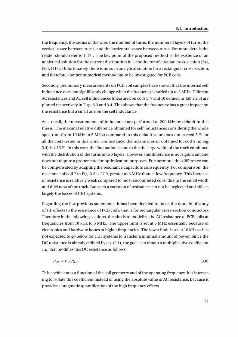
3.1. Introduction
the frequency, the radius of the wire, the number of turns, the number of layers of turns, the
vertical space between turns, and the horizontal space between turns. For more details the
reader should refer to [117]. The key point of the proposed method is the existence of an
analytical solution for the current distribution in a conductor of circular cross-section [54],
[93], [118]. Unfortunately, there is no such analytical solution for a rectangular cross-section,
and therefore another numerical method has to be investigated for PCB coils.
Secondly, preliminary measurements on PCB coil samples have shown that the internal self
inductance does not significantly change when the frequency is varied up to 5 MHz. Different
AC resistances and AC self inductances (measured on coils 5, 7 and 10 defined in Table 2.3) are
plotted respectively in Figs. 3.3 and 3.4. This shows that the frequency has a great impact on
the resistance but a small one on the self inductance.
As a recall, the measurements of inductance are performed at 200 kHz by default in this
thesis. The maximal relative difference obtained for self inductances considering the whole
spectrum (from 10 kHz to 5 MHz) compared to this default value does not exceed 5 % for
all the coils tested in this work. For instance, the maximal error obtained for coil 5 (in Fig.
3.4) is 4.13 %. In this case, the fluctuation is due to the the large width of the track combined
with the distribution of the turns in two layers. However, this difference is not significant and
does not require a proper care for optimization purposes. Furthermore, this difference can
be compensated by adapting the resonance capacitors consequently. For comparison, the
resistance of coil 7 in Fig. 3.3 is 27 % greater at 5 MHz than at low frequency. This increase
of resistance is relatively weak compared to most encountered coils, due to the small width
and thickness of the track. But such a variation of resistance can not be neglected and affects
largely the losses of CET systems.
Regarding the few previous statements, it has been decided to focus the domain of study
of HF effects to the resistance of PCB coils, that is for rectangular cross-section conductors.
Therefore in the following sections, the aim is to modelize the AC resistance of PCB coils at
frequencies from 10 kHz to 5 MHz. The upper limit is set at 5 MHz essentially because of
electronics and hardware issues at higher frequencies. The lower limit is set at 10 kHz as it is
not expected to go below for CET systems to transfer a minimal amount of power. Since the
DC resistance is already defined by eq. (2.1), the goal is to obtain a multiplicative coefficient
r AC that modifies this DC resistance as follows:
RAC = r AC RDC (3.8)
This coefficient is a function of the coil geometry and of the operating frequency. It is interest-
ing to isolate this coefficient instead of using the absolute value of AC resistance, because it
provides a pragmatic quantification of the high frequency effects.
57
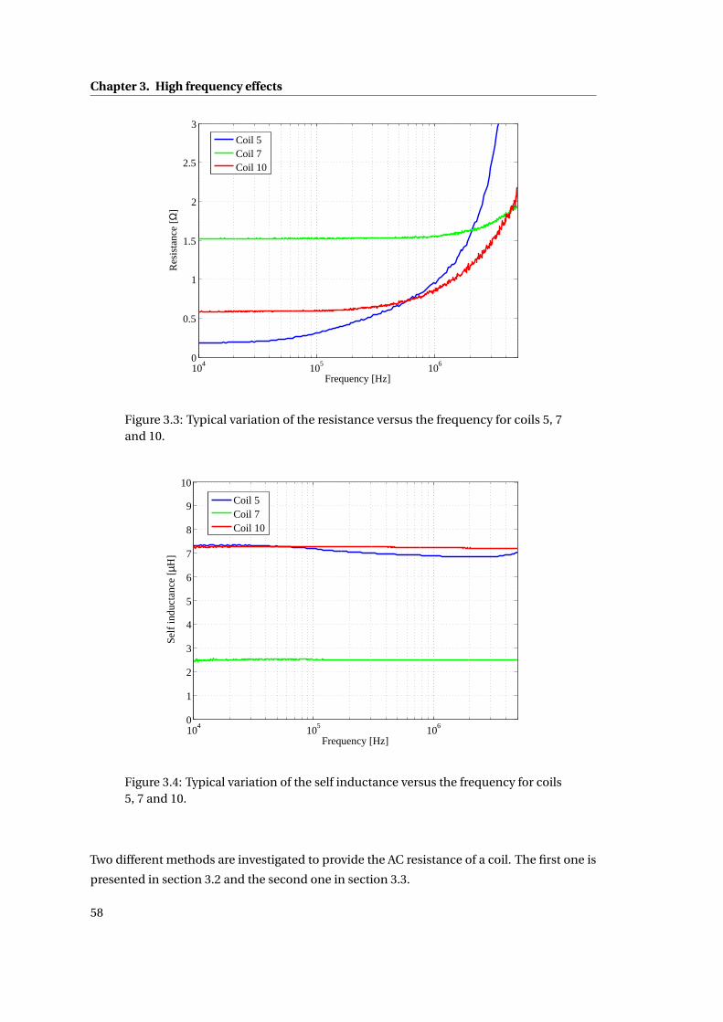
Chapter 3. High frequency effects
104
105
106
0
0.5
1
1.5
2
2.5
3
Frequency [Hz]
Res
ista
nce
[Ω]
Coil 5Coil 7Coil 10
Figure 3.3: Typical variation of the resistance versus the frequency for coils 5, 7and 10.
104
105
106
0
1
2
3
4
5
6
7
8
9
10
Frequency [Hz]
Self
indu
ctan
ce [µ
H]
Coil 5Coil 7Coil 10
Figure 3.4: Typical variation of the self inductance versus the frequency for coils5, 7 and 10.
Two different methods are investigated to provide the AC resistance of a coil. The first one is
presented in section 3.2 and the second one in section 3.3.
58

3.2. First numerical method
3.2 First numerical method
3.2.1 Current density modeling
This numerical method is based on [26]. The first step to modelize the high frequency effects
consists in evaluating the current distribution on the cross-section of the conductor. The
shape of the cross-section as well as the number of parallel conductors are also free parameters
in this method. Furthermore, the conductors are assumed to be infinite in length and the
current flows in the z-direction only.
Through a theoretical development that can be found in [26], [65], [109], the magnetic vector
potential, that is also solely z-directed, is given in the (x, y)-plane by:
A(x, y) = µ0
2π
∫S
J (x ′, y ′) ln√
(x −x ′)2 + (y − y ′)2d x ′d y ′ (3.9)
where S is the cross section of the conductor. The current density J(x, y) is defined by the
integral equation:
J (x, y) =− jωµ0σ
2π
∫S
J (x ′, y ′) ln√
(x −x ′)2 + (y − y ′)2d x ′d y ′+ Jω=0(x, y) (3.10)
Here, µ0 is the permeability of free space, σ is the conductivity of the copper, and Jω=0(x, y) =−σ|∇V | is the current density generated by the voltage supply, and corresponds to the current
density at low frequencies. By solving this last equation, it is possible to calculate the current
density distribution over the cross-section. But, except for a circular cross-section, it has no
analytical solution, that is why a numerical one is used to solve the problem. It is an integral
equation with the unknown function J (x, y). As it is not possible to solve it under this form, it
will be approximated by a matrix equation and then solved by inversion.
To do so, the cross-section is divided into multiple rectangular subbars, as shown in Fig. 3.5.
Each subbar can be different in width wi and thickness ti , resulting in a section Si . If the
subbars are sufficiently small (that is smaller than half the skin depth), the current density can
be assumed constant over their cross-section. It allows to rewrite equation (3.10) under the
59

Chapter 3. High frequency effects
form of a sum, as follows:
J (xm , ym) =− jωµ0σ
2π
N∑n=1
J (xn , yn)∫
Sn
ln√
(xm −x ′)2 + (ym − y ′)2d x ′d y ′+ Jω=0(xm , ym) (3.11)
Here, (xm , ym) is the position of the m-th subbar.
w
t
wi
ti(xi,yi)
y
x
Figure 3.5: Conductor of rectangular cross-section.
In order to transform equation (3.11) into a matrix form, it is necessary to solve the integral of
this last equation. Three different computation methods can be used [63], [110], [109], [65],
and are discussed in appendix B. They lead to the determination of the integral:
Qmn =∫
Sn
ln√
(xm −x ′)2 + (ym − y ′)2d x ′d y ′ (3.12)
and equation (3.11) takes the simpler form:
J (xm , ym) =− jωµ0σ
2π
N∑n=1
J (xn , yn)Qmn + Jω=0(xm , ym) (3.13)
Equation (3.11) may be applied for all subbars m = 1, . . . , N . This gives a set of complex
equations that can be written using matrix notation:c1,1 +1 c1,2 · · · c1,N
c2,1 c2,2 +1 · · · c2,N...
.... . .
...
cN ,1 cN ,2 · · · cN ,N +1
J1
J2...
JN
=
Jω=0,1
Jω=0,2...
Jω=0,N
(3.14)
60

3.2. First numerical method
with J1 = J (x1, y1), J2 = J (x2, y2),. . . JN = J (xN , yN ) and the coefficients cmn defined as follows:
cmn = jωµ0σQmn
2π(3.15)
Equation (3.14) can be expressed under its algebraic form:
(C+U )J =Jω= (3.16)
where U is the unit matrix, C is the matrix of the coefficients ckl , J is the vector of the z-
oriented current densities and Jω= the vector of the current densities at a zero-frequency.
Solving (3.16) allows to compute the current density for every subbar, and the distribution of
the potential vector A is calculated by resolving equation (3.9). With the assumption that the
current is constant over each subbar, the vector potential in the m-th subbar becomes:
Am = A(xm , ym) = µ0
2π
N∑n=1
JnQmn (3.17)
This way, the vector potential can be evaluated for every subbar.
3.2.2 Resistance calculation
Knowing the current distribution in the conductor, it is possible to calculate the linear resis-
tance Rl i n of the conductor. The idea consists in equating the total power dissipated in the
conductor S to the sum of the powers in every individual subbar as follows:
Rl i n |Itot |2 =N∑
n=1
ρ
Sn|In |2 = ρ
N∑n=1
|Jn |2Sn = ρ∫S
|J |2dS (3.18)
where Itot is the total current flowing in the conductor and is obtained by summing the
currents in each subbar as follows:
Itot =N∑
n=1In =
N∑n=1
JnSn =∫S
JdS (3.19)
Combining (3.18) and (3.19) yields the linear resistance:
Rl i n =ρ
∫S|J |2dS
|∫S
JdS|2 (3.20)
61

Chapter 3. High frequency effects
3.2.3 Internal self inductance calculation
In the introduction of this chapter, it is mentioned that it is not necessary to model the AC
self inductance, because its variation with the frequency is not significant. However, with the
method presented here, it is possible to calculate the internal part of the self inductance.
The linear internal self inductance Li ,l i n is also obtained using energy relations. The total
energy in the internal inductance is equated to the energy stored in the magnetic field within
the conductor, as follows:
Li ,l i n |Itot |2 =∫S
|∇× A|2dS = 1
µ0
∫S
|B |2dS = 1
µ0
N∑n=1
|Bn |2Sn (3.21)
As a remark, the factor 1/2 has been removed from both sides of the equation. This leads to
the following formulation for the linear internal inductance:
Li ,l i n = 1
µ0
∫S|B |2dS
|∫S
JdS|2 (3.22)
Therefore, to be able to compute Li ,l i n , it is necessary to evaluate the magnetic flux density B.
Since the the vector potential is solely z-directed, the magnetic flux density has two spatial
components along x-axis and y-axis, and is zero along z-axis (Bz = 0):
B =∇×A=
+∂A∂y
−∂A∂x
0
=
Bx
By
0
(3.23)
With equations (3.23) and (3.17), it is possible to calculate the magnetic flux density in the
center position of each subbar Sm as follows:
Bm,x = Bx (xm , ym) = µ0
2π
N∑n=1
Jn∂Qmn
∂y(3.24)
Bm,y = By (xm , ym) =−µ0
2π
N∑n=1
Jn∂Qmn
∂x(3.25)
where Bm,x and Bm,y are respectively the magnetic flux density in the x- and y-directions. The
norm is then easily calculated with the relation:
|Bm | =√
B 2m,x +B 2
m,x (3.26)
62

3.2. First numerical method
The numerical methods used to compute ∂Qmn/∂x and ∂Qmn/∂y are presented in appendix B.
3.2.4 Validation and measurements
To verify this model, two series of comparisons are made. The first one takes advantage from
that the numerical method can be applied to any conductor shape. More specifically, it means
that the subbars can be arranged at will so as to create the desired conductor shape. Then, a
convenient way to verify the accuracy of the model consists in applying it to a case which has
an analytical solution. For example, the skin effect for a conductor with circular cross-section
has an analytical solution which can therefore easily be compared to the computation method
proposed in this section.
At low frequencies, the linear resistance and the internal self inductance are given respectively
by Rdc,l i n = ρ/S, and Li ,l i n =µ0/8π. For a circular copper conductor with a radius of 0.1 mm,
the linear resistance and linear internal inductance are given respectively by 0.54Ω/m and
50.00 nH/m. The values obtained with the model presented in this section are 0.54Ω/m and
49.92 nH/m. Furthermore, it is also interesting to validate the model for higher frequencies. To
do this, the well-known analytical equations of the linear resistance and internal inductance
for a circular cross-section are used [54], [93], [118]. Their formulation is given in appendix
B.4 and are compared in Fig. 3.6 with the numerical method for different conductors radii.
Here as well, the size of the subbars is chosen so that their width wi and thickness ti are at
least smaller than half the skin depth. The results do match very well.
102
104
106
108
1010
0.5
1
1.5
2
2.5
3
3.5
4
4.5
5
5.5
6
Frequency [Hz]
Nor
mal
ized
res
ista
nce,
R AC/R
DC [−
]
Analytical sol., r=1 mmNumerical sol., r=1 mmAnalytical sol., r=0.1 mmNumerical sol., r=0.1 mmAnalytical sol., r=0.01 mmNumerical sol., r=0.01 mm
102
104
106
108
1010
0
0.2
0.4
0.6
0.8
1
Frequency [Hz]
Nor
mal
ized
inte
rnal
sel
f ind
ucta
nce,
Li,A
C/L
i,DC [−
]
Analytical sol., r=1 mm
Numerical sol., r=1 mm
Analytical sol., r=0.1 mm
Numerical sol., r=0.1 mm
Analytical sol., r=0.01 mm
Numerical sol., r=0.01 mm
(a) (b)
Figure 3.6: Comparison between the analytical solution and the numerical onefor the linear resistance (a) and for the linear internal inductance (b). The linearresistance and the linear internal inductance are normalized to the DC value.
In the second set of comparisons, the numerical solutions are compared with measurements
performed on real coils. According to [112], the numerical method provides more accurate
63

Chapter 3. High frequency effects
results by considering a number of neighboring conductors that is below the number of
turns of the coil. This assumption is assessed by varying the number of parallel conductors
during the computation of the AC resistance. Fig. 3.7 shows the comparison for coils 4,
5, 7 and 10 (defined in Table 2.3). The impedances have been measured using an Agilent
precision impedance analyzer 4294A (40 Hz-110 MHz). The real and imaginary parts of the coil
impedance are exported to Matlab and treated using equations (3.2) and (3.3) so as to retrieve
its AC resistance. This AC resistance is then normalized to the DC resistance, which gives the
multiplicative coefficient r AC .
104
105
106
0.5
1
1.5
2
2.5
3
Frequency [Hz]
Nor
mal
ized
res
ista
nce,
R AC/R
DC [−
]
Computed with 2 layers of 1 conductorComputed with 2 layers of 5 conductorsComputed with 2 layers of 10 conductorsComputed with 2 layers of 14 conductorsMeasured
104
105
106
0
1
2
3
4
5
6
7
8
Frequency [Hz]
Nor
mal
ized
res
ista
nce,
R AC/R
DC [−
]
Computed with 2 layers of 1 conductorComputed with 2 layers of 5 conductorsComputed with 2 layers of 9 conductorsMeasured
(a) (b)
104
105
106
0.95
1
1.05
1.1
1.15
1.2
1.25
1.3
1.35
Frequency [Hz]
Nor
mal
ized
res
ista
nce,
R AC/R
DC [−
]
Computed with 1 conductorComputed with 5 conductorsComputed with 10 conductorsMeasured
104
105
106
0.5
1
1.5
2
2.5
3
3.5
4
Frequency [Hz]
Nor
mal
ized
res
ista
nce,
R AC/R
DC [−
]
Computed with 1 conductorComputed with 10 conductorsComputed with 15 conductorsMeasured
(c) (d)
Figure 3.7: Comparison between the numerical solution and the measurementson (a) coil 4, (b) coil 5, (c) coil 7, and (d) coil 10.
The results of the comparison between the numerical model and the measurements have
to be analyzed. First, the model is good, since the relative difference rarely exceeds 30 %,
which is not a bad score considering the complexity of high frequency effects. In the four
considered coils, a maximal relative difference of 33 % is obtained for coil 5 at the highest
frequency. Secondly, the assumption made in [112], stating that the number of neighboring
64

3.3. Numerical modeling using FEM
conductors has to be adapted according to the tested coil has revealed to be true. This is an
issue because it is difficult, in a designing process, to guess a priori the number of conductors
to be evaluated for the coils.
As a conclusion for this first numerical method, our opinion is that it is well suited to generate a
general evaluation of the AC resistance for the design of CET systems. However, it is considered
insufficient for an optimization purpose.
3.3 Numerical modeling using FEM
3.3.1 Introduction
In this section, the second numerical method is discussed. It is based on finite element (FE)
models and simulations to evaluate the AC resistance of the coils.
For the design and optimization of systems that are too complex to be studied analytically
(or in which the analytical solution simply does not exist), the finite element method (FEM)
appears to be an interesting candidate. It consists of a numerical technique that allows to
resolve the differential equations describing a physical system. The solution obtained is an
approximation resulted from the subdivision of a complicated domain into multiple smaller
regions in which the governing equations are more easily solved. The approximation becomes
more accurate when the number of subregions is increased, but in return requires more
computational time and effort.
The FE software used, Flux from Cedrat [20], can solve electromagnetic and thermal physics
problems, both in two dimensions and three dimensions. It has proven to be capable of
computing Eddy currents in metallic materials, and of handling skin and proximity effects
in conductors [35], [73], [117]. In this section, the two-dimensional Flux2d will be used. The
following developments describe how simulations are carried out and how the resistance of
the simulated coils is extracted.
3.3.2 Geometrical structure and model of a coil
As the current in the conductors is assumed to be sinusoidal, the simulations for estimating
the skin and proximity effects are performed using the steady state AC magnetic 2D module.
In this section, the FE model of a coil will be represented through a simple but typical example.
Fig. 3.8 shows the geometrical description of this example, in which the conductors are
artificially enlarged for readability purposes.
65
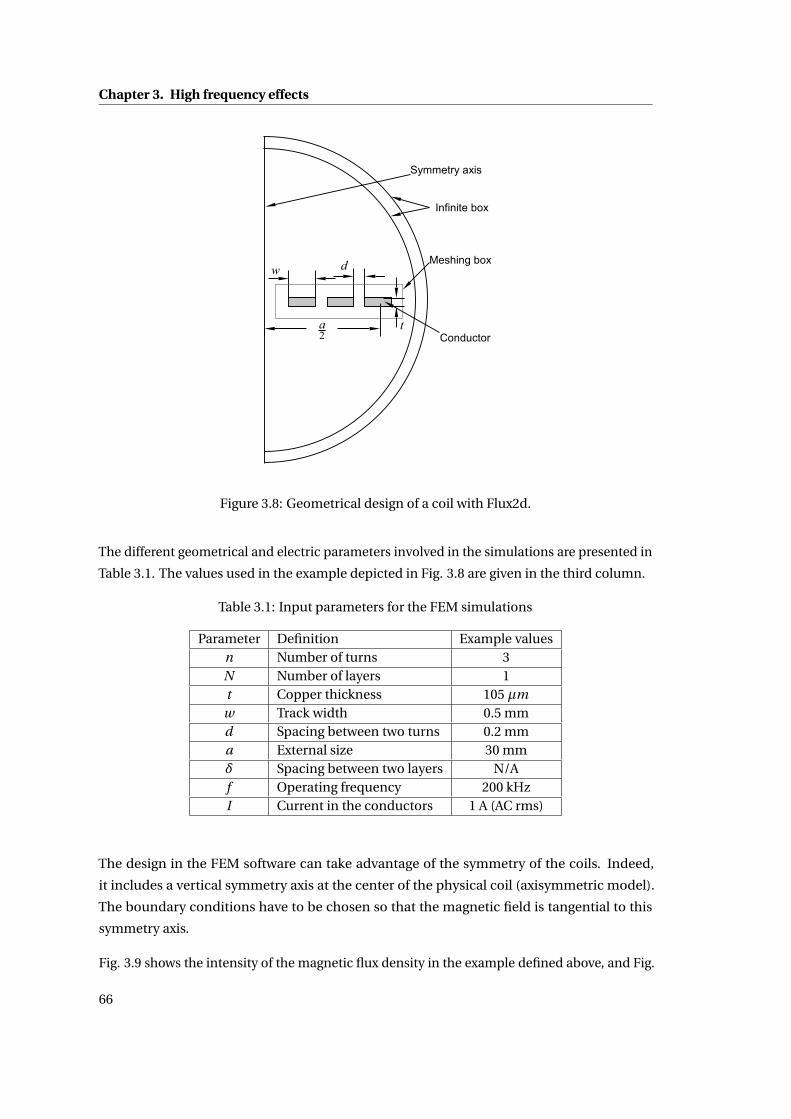
Chapter 3. High frequency effects
10.25 4.41w d
3.41t44.80a
2
Infinite box
Meshing box
Conductor
Symmetry axis
Figure 3.8: Geometrical design of a coil with Flux2d.
The different geometrical and electric parameters involved in the simulations are presented in
Table 3.1. The values used in the example depicted in Fig. 3.8 are given in the third column.
Table 3.1: Input parameters for the FEM simulations
Parameter Definition Example valuesn Number of turns 3N Number of layers 1t Copper thickness 105 µmw Track width 0.5 mmd Spacing between two turns 0.2 mma External size 30 mmδ Spacing between two layers N/Af Operating frequency 200 kHzI Current in the conductors 1 A (AC rms)
The design in the FEM software can take advantage of the symmetry of the coils. Indeed,
it includes a vertical symmetry axis at the center of the physical coil (axisymmetric model).
The boundary conditions have to be chosen so that the magnetic field is tangential to this
symmetry axis.
Fig. 3.9 shows the intensity of the magnetic flux density in the example defined above, and Fig.
66
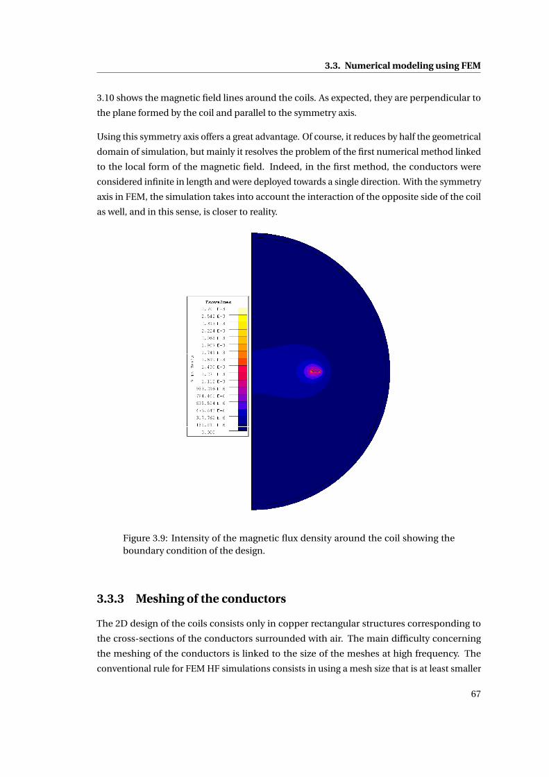
3.3. Numerical modeling using FEM
3.10 shows the magnetic field lines around the coils. As expected, they are perpendicular to
the plane formed by the coil and parallel to the symmetry axis.
Using this symmetry axis offers a great advantage. Of course, it reduces by half the geometrical
domain of simulation, but mainly it resolves the problem of the first numerical method linked
to the local form of the magnetic field. Indeed, in the first method, the conductors were
considered infinite in length and were deployed towards a single direction. With the symmetry
axis in FEM, the simulation takes into account the interaction of the opposite side of the coil
as well, and in this sense, is closer to reality.
Figure 3.9: Intensity of the magnetic flux density around the coil showing theboundary condition of the design.
3.3.3 Meshing of the conductors
The 2D design of the coils consists only in copper rectangular structures corresponding to
the cross-sections of the conductors surrounded with air. The main difficulty concerning
the meshing of the conductors is linked to the size of the meshes at high frequency. The
conventional rule for FEM HF simulations consists in using a mesh size that is at least smaller
67

Chapter 3. High frequency effects
Figure 3.10: Magnetic field lines zoomed in the conductors region.
or equal to half the skin depth. The skin depth is defined as follows:
δsd = 1√π f µ0σ
(3.27)
where µ0 is the magnetic permeability and ρ the resistivity of the conductor.
Considering copper as the conductive material and the highest frequency of 5 MHz for the
current application, the resulting skin depth is equal to 30 µm. Following the rule formulated
above, the mesh size for the conductors is set to 15 µm. In order to reduce the number of
elements for the simulations and to increase the quality of the meshing, an intermediate box is
created around the conductors where the mesh size is refined, as shown in Fig. 3.8. A practical
example of the meshing box and the meshing of conductors is shown in Fig. 3.11.
3.3.4 Physical and electrical definition
Each turn of the coil is physically represented in the simulation by a rectangular solid con-
ductor. Then, all these conductors are electrically connected in series and are supplied by a
current source of I = 1 A (AC rms). Fig. 3.12(a)-(b) gives two examples of the current density
distribution inside the conductors, respectively at 200 kHz and 5 MHz. At 200 kHz the current
distribution is nearly uniform on the entire cross-sections, and at 5 MHz, there is an obvious
crowding of current at their periphery.
The strategy to evaluate the resistance of the coil consists then in computing the Joule losses
68

3.3. Numerical modeling using FEM
Figure 3.11: Meshing of the intermediate box and the conductors.
(a)
(b)
Figure 3.12: Current density distribution in the conductors at (a) 200 kHz and (b)5 MHz.
inside the conductors with:
P j =∫S
ρ J 2dS (3.28)
where S is the surface defined by the conductors and J the current density. Knowing the
69

Chapter 3. High frequency effects
current I that is generated in the conductors, the resistance RAC can be deduced from:
RAC = P j
I 2 (3.29)
The value obtained is then normalized to the DC resistance obtained with (2.1) so as to obtain
the multiplication coefficient r AC .
3.3.5 Validation and measurements
To validate the FEM model, comparisons with measurements are performed on coils 4, 5,
6, 7, 10, 11 (defined in Table 2.3). The results are shown in Fig. 3.13. The conditions of
measurements are the same as those defined in Section 3.2.4.
The FEM solution was first thought to be used as a verification for the first numerical method,
but at last it appeared to be much more accurate than it according to the measurements. For
every coils tested in this work, the relative error between FEM computations and measure-
ments rarely exceeds 15 %. For example, the largest relative difference (of 19.5 %) for the 6 coils
compared in Fig. 3.13 is obtained for coil 6 at about 800 kHz.
As a conclusion, the FEM method provides more accurate results than the first method.
An error that generally remains below 15 % is really good for the AC resistance of a coil.
Furthermore, the FEM method does not require to adjust the number of conductors to be
modeled.
3.4 Discussion
Both methods have different advantages and drawbacks. In summary, the first method,
presented in section 3.2, is less expensive in terms of computation time but provides less
accurate results. Our belief is that this first method is sufficient for general design purposes
and prototyping. However, for an optimization method, more accurate results are preferable
so as to prevent an eventual erroneous convergence.
The second method, presented in section 3.3, provides more accurate results but in return
is much more time consuming, since it is necessary to launch the FEM software, create the
meshing, solve the equations and retrieve the results. Knowing that one simulation can easily
last more than one minute, this solution can definitely not be applied by direct means to the
optimization process, in which the number of simulations is expected to be in the order of
40’000.
70

3.4. Discussion
104
105
106
0.5
1
1.5
2
2.5
3
Frequency [Hz]
Nor
mal
ized
res
ista
nce,
R AC/R
DC [−
]
SimulatedInterpolatedMeasured
104
105
106
0
1
2
3
4
5
6
7
8
Frequency [Hz]
Nor
mal
ized
res
ista
nce,
R AC/R
DC [−
]
SimulatedInterpolatedMeasured
(a) (b)
104
105
106
1
1.5
2
2.5
3
3.5
4
4.5
5
5.5
6
Frequency [Hz]
Nor
mal
ized
res
ista
nce,
R AC/R
DC [−
]
SimulatedInterpolatedMeasured
104
105
106
0.95
1
1.05
1.1
1.15
1.2
1.25
1.3
Frequency [Hz]
Nor
mal
ized
res
ista
nce,
R AC/R
DC [−
]
SimulatedInterpolatedMeasured
(c) (d)
104
105
106
0.5
1
1.5
2
2.5
3
3.5
4
Frequency [Hz]
Nor
mal
ized
res
ista
nce,
R AC/R
DC [−
]
SimulatedInterpolatedMeasured
104
105
106
0
1
2
3
4
5
6
7
Frequency [Hz]
Nor
mal
ized
res
ista
nce,
R AC/R
DC [−
]
SimulatedInterpolatedMeasured
(e) (f)
Figure 3.13: Comparison between measured and computed AC resistance. TheAC resistance is normalized to the DC resistance. (a) Coil 4, (b) Coil 5, (c) Coil 6,(d) Coil 7, (e) coil 10, (f) coil 11.
71

Chapter 3. High frequency effects
Therefore, the simulations have to be exploited in a way that make them usable in the op-
timization method. This issue is discussed in the following section. Then, some practical
observations are made in section 3.6 concerning the effect of the high frequency on the coils
and more generally on CET systems.
3.5 Exploitation of FEM simulations
3.5.1 Design of experiments
The concepts of design of experiments (DOE) are thoroughly discussed in [52]. It consists basi-
cally in a strategy for planning the experiments linked to a given research problem. Properly
designed experiments allow to retrieve a maximum of information from as few experimental
tests as possible. The results thus obtained can be analyzed using relatively simple statistical
tools that make the information easily readable and interpretable.
DOE techniques are generally used in practical measurements or tests, more rarely in simula-
tions. But DOE applied to FEM simulations has been successfully performed in numerous
works [52], [98], [84]. Therein, each different experimental run would require its own proto-
type which is most often inconceivable in electromagnetic applications. In this sense it is
advantageous to replace the practical measurements by simulations.
Theoretically, DOE can be used to model a system in its entire experimental domain with only
a few simulations, the number of necessary experimental runs depending on the design itself.
Traditionally, the most common plan of experiments consists in varying one parameter at
a time, all the other ones being held constant. Such a simple plan only allows to study the
effect of the concerned factor on the system, and does not take into account the possible
interactions between factors. In this sense, well structured plans (or designs) bring along a
substantial improvement, as all parameters are simultaneously varied. Many different designs
do exist, such as full factorial designs, fractional designs, Hadamard designs or composite
designs. Every design has its advantages and drawbacks, but in this thesis, only full factorial
designs are used.
In full factorial designs, the parameters are generally evaluated on two levels that correspond
to their lower and upper limit. Then, to model a system defined by 5 parameters, the number
of required experiments is 25 = 32. With such a design, it is possible to generate a polynomial
linear model that takes into account the interactions between factors.
In the specific case, the number of variables can be reduced to 5. First knowing that the
number of layers for the turns distribution is either one or two, both cases can be treated
72
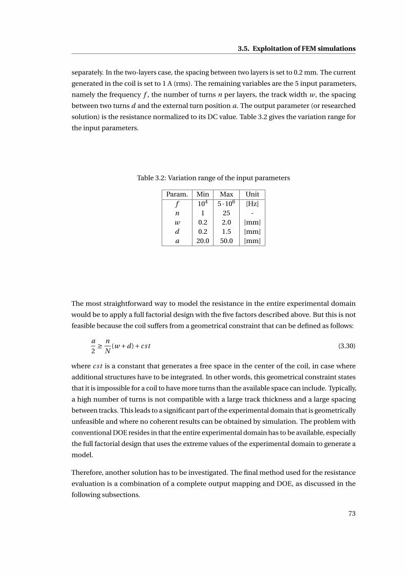
3.5. Exploitation of FEM simulations
separately. In the two-layers case, the spacing between two layers is set to 0.2 mm. The current
generated in the coil is set to 1 A (rms). The remaining variables are the 5 input parameters,
namely the frequency f , the number of turns n per layers, the track width w , the spacing
between two turns d and the external turn position a. The output parameter (or researched
solution) is the resistance normalized to its DC value. Table 3.2 gives the variation range for
the input parameters.
Table 3.2: Variation range of the input parameters
Param. Min Max Unitf 104 5 ·106 [Hz]n 1 25 -w 0.2 2.0 [mm]d 0.2 1.5 [mm]a 20.0 50.0 [mm]
The most straightforward way to model the resistance in the entire experimental domain
would be to apply a full factorial design with the five factors described above. But this is not
feasible because the coil suffers from a geometrical constraint that can be defined as follows:
a
2≥ n
N(w +d)+ cst (3.30)
where cst is a constant that generates a free space in the center of the coil, in case where
additional structures have to be integrated. In other words, this geometrical constraint states
that it is impossible for a coil to have more turns than the available space can include. Typically,
a high number of turns is not compatible with a large track thickness and a large spacing
between tracks. This leads to a significant part of the experimental domain that is geometrically
unfeasible and where no coherent results can be obtained by simulation. The problem with
conventional DOE resides in that the entire experimental domain has to be available, especially
the full factorial design that uses the extreme values of the experimental domain to generate a
model.
Therefore, another solution has to be investigated. The final method used for the resistance
evaluation is a combination of a complete output mapping and DOE, as discussed in the
following subsections.
73

Chapter 3. High frequency effects
3.5.2 Complete output mapping
Definition
A complete output mapping consists in generating the solutions of the problem for all possible
combinations of parameters. For continuous variables, some predetermined values within
their variation range have to be fixed. The number of these values will determine the number
of simulations to be done and therefore influence drastically the computation time. The result
is a grid of points that are distributed in the experimental domain.
The goal is then to predict the solution for a point where no simulation has been performed.
The simplest method is to choose the existing combination of parameters that comes clos-
est to the desired evaluation point. A more complex approach is to guess the solution by
interpolation.
The challenge consists then in realizing a huge number of simulations and saving the data in a
form that is easily and quickly accessible during an optimization process. In the present case,
the simulations can take advantage of the FEM software to simplify the management of data.
By creating a specific scenario during the solving of the simulations, it is possible to define
the frequency f as a variable parameter and then to compute the solutions for a single coil at
multiple different frequencies.
The complete output mapping is fully managed by Matlab. A routine has been created that
allows to launch automatically the simulations with the desired set of parameters and then to
retrieve the results. A total grid of 500’000 points have been evaluated this way, and the results
have been stored in text files that are quickly accessible for further use.
Interpolation Strategy
As already mentioned, the simplest way to find the solution for a random point in the exper-
imental domain is to choose the one of the complete output mapping that is closest. This
strategy can easily be tested using 2000 samples randomly chosen in the experimental domain.
Fig. 3.14 shows the discrepancy between FEM simulation and the complete output mapping
with the closest pick for these 2000 points. Obviously this strategy gives rise to errors that
could be avoided by performing interpolations.
First, let us note that the number of turns n does not require any interpolation since it can
take only integer values. Then, two different types of interpolation are used for the different
parameters of Table 3.2. The first interpolation concerns the frequency f .
During the simulation, the resistance of the coil is calculated for 10 different values evenly
74

3.5. Exploitation of FEM simulations
−15 −10 −5 0 5 10 15 200
1
2
3
4
5
6
Discrepancy [%]
Sam
ples
[%]
Closest pick
Figure 3.14: Discrepancy between FEM simulations and the complete outputmapping used with the closest pick strategy. A total of 2000 samples randomlygenerated in the experimental domain have been evaluated.
distributed inside the frequency variation range. To evaluate the resistance for intermediate
values situated between those 10 ones, a spline interpolation is applied.
The second interpolation concerns the track width w , the spacing between two tracks d and
the external turn position a. For these three parameters, a factorial plan can be applied to the
complete output mapping in order to generate a linear model between each of its points. Two
different models have been tested using the same 2000 random samples as in Fig. 3.14: the
linear model with interactions and the linear model without interactions.
Fig. 3.15 shows the discrepancy between FEM simulations and the complete output mapping
with both interpolations discussed above. They are in good agreement. The difference between
the model with interactions and the model without interactions is not significant, but the
former is preferred as its issued standard deviation (std = 0.41) is slightly lower than for the
latter (std = 0.42). For comparison, the standard deviation obtained with the closest pick
strategy was much larger (std = 3.41).
75

Chapter 3. High frequency effects
−4 −3 −2 −1 0 1 2 3 40
5
10
15
20
25
30
35
40
45
50
Discrepancy [%]
Sam
ples
[%]
With interactionsWithout interactions
Figure 3.15: Discrepancy between FEM simulations and the complete outputmapping with interpolation. The results obtained from the model with interac-tions and without interactions are compared. The same 2000 samples as in Fig.3.14 have been evaluated.
3.6 Effective impact of the high frequency on CET
An good manner to verify if it is advantageous for a certain coil to increase the operating
frequency is to compute its quality factor (2.18) on the whole frequency range. Fig. 3.16 shows
the quality factor Q as a function of the frequency for the coils measured in Fig. 3.13. For
all tested coils, the increase of resistance with the frequency is lower than the increase of
inductive reactance. Therefore the quality factor can be only increased with the frequency.
This statement can be generalized for all PCB coils in the frequency range considered in
this thesis, given that the condition (3.5) is respected. As a result, it seems advantageous
to work at the highest operating frequency as possible. However, the quality factor defines
the coils individually whereas a CET system is much more complex and involves additional
components (multiple coils, electronics, devices to be supplied, . . . ) that bring other issues at
high frequency. At this point it is too early to state that the highest operating frequency is the
best suited. This can be easily verified by evaluating the losses in a coreless transformer when
the frequency is varied and the output power is fixed.
Then, to measure the impact of the high frequency on CET systems, an example using the
coreless transformer composed of coils 5 and 6 as respective primary and secondary coils is
proposed. The efficiency of the coreless transformer and the power losses are plotted versus
76

3.7. Overall conclusion
the frequency in Fig. 3.17. Two cases are represented. In the first one, the HF effects are not
taken into account (the DC value of the resistances is used over the whole frequency range),
and in the second one, they are taken into account. In this example, the current of the primary
coil is adjusted so as to obtain exactly 5 W on a load resistance of 10Ω.
104
105
106
0
10
20
30
40
50
60
70
80
90
100
Frequency [Hz]
Qua
lity
fact
or, Q
[−]
Coil 4Coil 5Coil 6Coil 7Coil 10Coil 11
Figure 3.16: Computed quality factor for different coils.
This example shows how crucial it is to take into account the variation of the resistance with
the frequency. As this variation depends on the coils geometry as well, a deeper analyzis of
complete CET systems and the inherent losses has to be performed in order to obtain an
optimal solution. This matter is discussed in the next chapter.
3.7 Overall conclusion
As an overall conclusion, two methods to characterize the HF effects have been presented.
After comparison, the FEM method has been chosen for the forthcoming optimization since it
provided more accurate results. The main issue from this method is the computation time
that was not acceptable, knowing that the average time for a single evaluation is more than
one minute.
Therefore, a complete output mapping and an interpolation strategy using DOE have been
implemented in order to exploit effectively the results of FEM simulations. Doing so allows
to reduce the evaluation time of a single coil to about 0.2 seconds compared to more than
60 seconds that would be required to perform the full simulation. The final result offers an
77
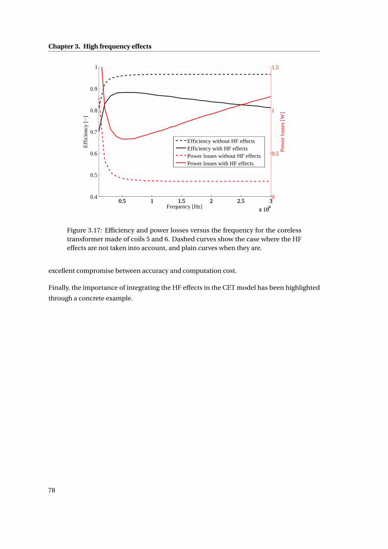
Chapter 3. High frequency effects
0.5 1 1.5 2 2.5 3
x 106
0.4
0.5
0.6
0.7
0.8
0.9
1
Effi
cien
cy [−
]
0.5 1 1.5 2 2.5 3
x 106
0
0.5
1
1.5
Pow
er lo
sses
[W]
Frequency [Hz]
Efficiency without HF effectsEfficiency with HF effectsPower losses without HF effectsPower losses with HF effects
Figure 3.17: Efficiency and power losses versus the frequency for the corelesstransformer made of coils 5 and 6. Dashed curves show the case where the HFeffects are not taken into account, and plain curves when they are.
excellent compromise between accuracy and computation cost.
Finally, the importance of integrating the HF effects in the CET model has been highlighted
through a concrete example.
78

CHAPTER 4
Design and optimization of CET
systems
Summary
4.1 Problem definition . . . . . . . . . . . . . . . . . . . . . . . . . . . . . . . . . . 80
4.2 Sensitivity analyzis . . . . . . . . . . . . . . . . . . . . . . . . . . . . . . . . . . 83
4.2.1 Analyzis context . . . . . . . . . . . . . . . . . . . . . . . . . . . . . . . . . 83
4.2.2 Effect of the number of turns . . . . . . . . . . . . . . . . . . . . . . . . . 83
4.2.3 Effect of the track width . . . . . . . . . . . . . . . . . . . . . . . . . . . . 85
4.2.4 Effect of the space between tracks . . . . . . . . . . . . . . . . . . . . . . 85
4.2.5 Effect of the size of the coils . . . . . . . . . . . . . . . . . . . . . . . . . . 86
4.2.6 Effect of the displacement of the secondary coil . . . . . . . . . . . . . . 87
4.2.7 Effect of the frequency . . . . . . . . . . . . . . . . . . . . . . . . . . . . . 88
4.2.8 Discussion . . . . . . . . . . . . . . . . . . . . . . . . . . . . . . . . . . . . 90
4.3 Optimization methods . . . . . . . . . . . . . . . . . . . . . . . . . . . . . . . . 91
4.4 Genetic algorithms . . . . . . . . . . . . . . . . . . . . . . . . . . . . . . . . . . 92
4.4.1 Generalities . . . . . . . . . . . . . . . . . . . . . . . . . . . . . . . . . . . 92
4.4.2 Genetic algorithm implementation . . . . . . . . . . . . . . . . . . . . . 93
4.4.3 Genetic algorithm testing . . . . . . . . . . . . . . . . . . . . . . . . . . . 94
4.5 Multiobjective genetic algorithms . . . . . . . . . . . . . . . . . . . . . . . . . 98
4.5.1 Pareto optimality . . . . . . . . . . . . . . . . . . . . . . . . . . . . . . . . 98
Chapter 4. Design and optimization of CET systems
4.5.2 Generalities . . . . . . . . . . . . . . . . . . . . . . . . . . . . . . . . . . . 99
4.5.3 Multiobjective genetic operators . . . . . . . . . . . . . . . . . . . . . . . 100
4.5.4 Multiobjective genetic algorithm implementation . . . . . . . . . . . . 102
4.5.5 MOGA testing . . . . . . . . . . . . . . . . . . . . . . . . . . . . . . . . . . 103
4.6 Design of the CET table . . . . . . . . . . . . . . . . . . . . . . . . . . . . . . . 107
4.6.1 Context and specifications . . . . . . . . . . . . . . . . . . . . . . . . . . 107
4.6.2 Choice of the coils geometry . . . . . . . . . . . . . . . . . . . . . . . . . 108
4.6.3 Choice of the compensation topology . . . . . . . . . . . . . . . . . . . . 109
4.6.4 CET table Optimization . . . . . . . . . . . . . . . . . . . . . . . . . . . . 110
4.7 Overall conclusion . . . . . . . . . . . . . . . . . . . . . . . . . . . . . . . . . . 115
This chapter addresses the problem of CET systems design for most possible applications
realized using PCB coils. In this context the most interesting research purpose consists in
proposing a general methodology to find the optimal solution to each individual applications.
The first part of this chapter defines the CET problems to be optimized in general and in the
scope of this thesis. The second part proposes a sensitivity analyzis on the main parameters
for CET systems in order to give a better global understanding of coreless transformers and
possibly to simplify the forthcoming optimization. Then the optimization of CET systems is
discussed and a new genetic algorithm (GA) is developed and tested. Finally, this new GA is
applied to the design of the CET table.
4.1 Problem definition
The first chapters of this thesis have presented a good overview of the different choices that
an engineer faces when he has to design coreless transformers for CET applications. Among
these choices, one can find notably the compensation topology, the shape of the coils, the
number of layers for the turns distribution, the operating frequency and the input voltage or
current. Thus, designing a coreless transformer is not a trivial task. Frequently, the influence
of each parameter is analyzed individually so as to deduce the tendencies and then make a
choice. In this chapter, the goal is to present a method that is able to find the global optimum.
As pointed out in Chapter 1, two different kinds of CET systems can be optimized. The first
one concerns relatively simple applications involving a static coreless transformer with only
one primary coil and one secondary coil. The second one addresses more complicated CET
systems with multiple primary coils or multiple secondary coils working simultaneously. The
design of these two cases is approached with the same method in this chapter, but some
differences still remain.
Indeed, the former can be resolved in a straightforward way, by evaluating only a single
80

4.1. Problem definition
situation that corresponds to the case where both coils are well aligned, or where the CET
is most critical. The latter involves a larger charging surface, where a minimal amount of
power has to be ensured at every positions. Without going too much into details as this matter
will be discussed later in this work, such systems require multiple evaluations corresponding
to different scenarios that may occur during the CET process. In brief, both problems are
solved with the same optimization method, the main difference resides in the function to be
optimized. In this chapter, the focus is first made on the first kind of CET systems through
a simple problem that allows to test and validate the optimization algorithm. Then, the
optimization of the second kind of CET systems will be discussed in section 4.6, where the
goal is to design a CET table.
In general for CET systems, the specifications are based on the application to perform, and
generally concern the dimensions of the CET platform, the input voltage and output voltage,
or the power to be transferred. The design criteria tend to maximize the efficiency η or
maximize the power transferred to the load PL . In this thesis, as the application deals with
low consumption peripherals (≤ 5 W), it is difficult to obtain really high efficiencies (≥ 90 %)
because of the intrinsic nature of CET systems. Indeed, the addition of electronics and the
presence of intermediate primary and secondary coils generate losses that cannot be avoided.
This is the price to pay when using CET systems. But still, they can be minimized by making
the good choices. That is why, in our opinion, it is more adequate to use the losses Ploss as
design criterion instead of the efficiency. This is even more true considering that the main
limitation for CET is the heat generated by the current in the coils, which is directly linked to
the Joule losses.
This work is done in the academic world, where economical aspects are generally not an issue.
However, for the design of a future industrial application, they have to be kept in mind. In
the scope of this thesis, the goal consists in building prototypes that show and validate the
theoretical developments, and economical issues remain secondary but still can be anticipated
to some extent. Furthermore, the cost estimation for a prototype designed and built during
this work would be far from an industrial reality where the price of the components highly
depends on their quantity. This is even more true for PCBs as the price of a single PCB is really
high compared to a multitude of identical PCBs for which the price per units is drastically
reduced. In this sense, the PCB is a good candidate for the coils of a CET application, in
addition to some obvious advantages that it offers during the fabrication and integration.
With this description, two objective functions have to be optimized, i.e. the output power and
81

Chapter 4. Design and optimization of CET systems
the power losses:
O1 = Ploss [W ] (4.1)
O2 = −Pout [W ] (4.2)
Here, the first objective function O1 represents the sum of Joule losses generated in every
coil of the CET system, and O2 represents the total power transferred to the terminals of the
secondary coil. To Pout is assigned the negative sign because every optimization problem
discussed in this chapter are turned into a minimization problem.
At a first glance, minimizing those two objective functions seems equivalent to maximizing
the efficiency. In fact, the problem is much more subtle, and the experience shows that both
objective functions have to be used to obtain the desired result. The different ways to deal
with multiobjective problems is discussed later in this chapter.
One of the main difficulties concerning the design of CET systems is the number of parameters,
because the geometry is quite complicated. As the output power is generally defined by the
specifications, the remaining free parameters for CET systems are given in Table 4.1, where
indices 1 and 2 are used to characterize respectively the primary and the secondary coils.
Table 4.1: Free parameters of CET systems.
Parameter ValueSh1,2 The choice of the coils shape
To The choice of the compensation topologyUi n or Ii n The input voltage or the input current
f The operating frequencyN1,2 The number of layersn1,2 The number of turnsa1,2 The external dimension of the coilsw1,2 The track widthd1,2 The space between two trackst1,2 The copper thicknessg The air gap
The design comes up with a total of 18 parameters or choices for simple CET systems. Compli-
cated CET systems (that belong to the second kind described above) include additional factors
such as the number of primary and secondary coils and how they are distributed.
The variation of each single parameter leads to different solutions that could possibly fulfill
the specifications of a given application. From this point, the problem can be solved in several
82

4.2. Sensitivity analyzis
ways. Before going directly into optimization considerations, a good strategy consists in
performing a sensitivity analyzis on the different parameters.
The advantage of a sensitivity analyzis is threefold. First, it provides a general understanding
of the CET behavior and the impact of the main parameters on the whole system. Secondly, it
allows to determine which parameters can be fixed so as to lighten the optimization process.
Thirdly, it allows to determine the variation range of the parameters.
4.2 Sensitivity analyzis
4.2.1 Analyzis context
The goal of this section is to analyze the effect of the main geometrical parameters on CET
systems. As a design reference for this analyzis, the coreless transformer obtained with coils 5
and 6 (from Table 2.3) as primary and secondary coils is used. By default, the parameters of
both coils are the ones presented in Table 2.3. A PS compensation topology is used because it
is the one that will be used for the CET table. This choice will be justified later. Both capacitors
are assumed to be perfectly designed according to the resonance frequency of 250 kHz, and
the load is a resistor of 10Ω. The input voltage U1 applied to the coreless transformer is set to
12 V (rms).
4.2.2 Effect of the number of turns
In this first part, the effect of the number of primary turns n1 and secondary turns n2 is studied.
The geometrical definition of a coil is such that the first turns are placed on its external size.
The additional turns are then added towards the center of the coil by superimposed pairs. The
number of primary turns n1 is varied from 2 to 18 (i.e. n1 = 2,4, . . . ,18) and the number of
secondary turns is varied from 2 to 20 (i.e. n1 = 2,4, . . . ,20), and the other parameters are kept
constant.
Fig. 4.1(a) shows the mutual inductance L12 of the coreless transformer as a function of n1
and n2. As expected, the results show that the mutual inductance increases when the number
of primary and secondary turns is increased and that internal turns have less impact than
external ones.
Fig. 4.1(b) presents the output power Pout of the coreless transformers as a function of n1
and n2. The results show that when n2 is increased, the output power is also increased. On
the contrary, increasing n1 leads to a decrease of the output power. The reason is that the
impedance of the primary coil, given by Z 1 = R1 + jωL1, becomes greater with the number of
83

Chapter 4. Design and optimization of CET systems
turns and therefore limits the current IL1 flowing through it when a PS topology is used. From
the second voltage equation (2.23), it is obvious that it leads to a decrease of the secondary
current I2. Actually this effect dominates the increase of the mutual inductance. However,
using a small amount of primary turns so as to transfer a large power may be inappropriate in
terms of Joule losses and efficiency.
Fig. 4.1(c) presents the efficiency η of the coreless transformer as a function of n1 and n2. Only
the Joule losses are taken into account. The efficiency is thus defined as follows:
η= Pout
Pout +Pl oss(4.3)
So using a sufficiently large number of turns ensures to have a good efficiency, especially for
the number of secondary turns.
05
1015
20
0
10
200
2
4
6
n1 [−]n
2 [−]
Mut
ual i
nduc
tanc
e L 12
[µH
]
05
1015
20
0
10
200
10
20
30
40
n1 [−]
n2 [−]
Out
put p
ower
[W]
(a) (b)
05
1015
20
0
10
200
0.2
0.4
0.6
0.8
1
n1 [−]n
2 [−]
Effi
cien
cy [−
]
(c)
Figure 4.1: (a) Mutual inductance, (b) output power, and (c) efficiency versus thenumber of primary turns and the number of secondary turns.
84

4.2. Sensitivity analyzis
4.2.3 Effect of the track width
Here, the primary and secondary track widths w1 and w2 are varied while the other parameters
are kept at their default value except for n1 and n2 that are set to 12, which allows to have a
larger range variation for w1 and w2, that is from 0.2 mm to 2.0 mm (w1,2 = 0.2,0.4, . . . ,2.0 mm).
Thus, the external size of the coils remains unchanged (their default value being a1 = a2 =40 mm), and the position of the turns is automatically adapted according to the track width.
Fig. 4.2(a) presents the mutual inductance as a function of w1 and w2. The results show that
the mutual inductance is greater for small values of track widths. It is so because small track
widths allow to concentrate the turns at the periphery of the coils, which leads to an increase
of self and mutual inductances.
Figs. 4.2(b) and 4.2(c) present respectively the output power and the efficiency of the coreless
transformer as a function of w1 and w2. In this case, the sensitivity analyzis shows a great
interest because the results are not consistent with the intuition. The output power increases
when w1 is increased, and on the contrary decreases when w2 is increased. Also, one could
expect to obtain the best efficiency when the track widths are maximal, but actually this is not
true. Here, for example, the best efficiency is obtained for intermediate values of widths (that
are w1 = 1.2 mm and w2 = 0.8 mm). This is mainly due to the skin and proximity effects that
have a greater impact on larger track widths.
4.2.4 Effect of the space between tracks
Here, the space between two tracks d1 and d2 respectively for the primary and secondary coils
are varied from 0.2 mm to 1.5 mm (i.e. d1,2 = 0.2,0.3, . . . ,1.5 mm). n1 and n2 are set to 12 so as
to obtain the maximal range of variation for d1 and d2. The other parameters are kept at their
default value.
Fig. 4.3(a) shows the mutual inductance of the coreless transformer as a function of d1 and d2.
It is logically greater for small values of d1 and d2 as the turns are more concentrated at the
periphery of the coils.
Fig. 4.3(b) presents the output power as a function of d1 and d2. Increasing the primary inter-
track space causes the impedance of the primary coil and mutual inductance to decrease, and
then more current is generated into the primary coil which results in more transferred power.
On the contrary, increasing the secondary inter-track space leads to a decrease of the output
power.
As shown in Fig. 4.3(c), d1 does not have a great impact on the efficiency of the coreless
85

Chapter 4. Design and optimization of CET systems
00.5
11.5
2
0
1
2
2
3
4
5
6
w1 [mm]w
2 [mm]
Mut
ual i
nduc
tanc
e L
12 [µ
H]
00.5
11.5
2
0
1
2
0
2
4
6
8
w1 [mm]w
2 [mm]
Out
put p
ower
[W
]
(a) (b)
00.5
11.5
2
0
1
2
0.4
0.6
0.8
1
w1 [mm]w
2 [mm]
Effi
cien
cy [−
]
(c)
Figure 4.2: (a) Mutual inductance, (b) output power, and (c) efficiency versus theprimary track width and the secondary track width.
transformer. Even so it is slightly more interesting to have a small value for d2. Here again, the
maximal efficiency is obtained with intermediate values of d1 and d2 (that are d1 = 0.6 mm
and d2 = 0.5 mm), instead of the smallest values as intuition could suggest.
4.2.5 Effect of the size of the coils
Here, the external lengths a1 and a2 are varied from 28 mm to 50 mm. n1 and n2 are set to 12
so as to obtain a sufficiently large range of variation. The other parameters are kept at their
default value.
Fig. 4.4(a) shows the mutual inductance as a function of a1 and a2. Of course it becomes
greater when both coils become larger as well. But there is another condition to satisfy in order
to obtain a maximal mutual inductance, which is for both coils to have a similar external size.
Fig. 4.4(b) presents the output power as a function of a1 and a2. It is difficult to predict the
86

4.2. Sensitivity analyzis
00.5
11.5
0
0.5
1
1.5
2
2.5
3
3.5
4
d1 [mm]d
2 [mm]
Mut
ual i
nduc
tanc
e L
12 [µ
H]
00.5
11.5
0
0.5
1
1.5
2
4
6
8
d1 [mm]d
2 [mm]
Out
put p
ower
[W
]
(a) (b)
00.5
11.5
00.5
11.5
0.75
0.8
0.85
0.9
0.95
d1 [mm]d
2 [mm]
Effi
cien
cy [−
]
(c)
Figure 4.3: (a) Mutual inductance, (b) output power, and (c) efficiency versus theprimary inter-track space and the secondary inter-track space.
behavior of the output power. However, an interesting result is that using a larger secondary
coil than the primary one allows to increase the transferred power, as long as the difference in
size is not excessive.
Fig. 4.4(c) shows that it is interesting to have coils as large as possible in term of efficiency, and
this statement is equivalently valid for the primary and the secondary coils.
4.2.6 Effect of the displacement of the secondary coil
Here, the secondary coil is displaced above the primary one. The lateral displacements are
defined by xd along the X-axis and by yd along the Y-axis. The displacements are varied from
0 mm (which corresponds to the case where the coils are perfectly aligned) to 30 mm.
Fig. 4.5(a) shows the mutual inductance and Fig. 4.5(b) shows the output power as a function
of xd and yd . In this case, the primary coil does not undergo a change of impedance as its
87

Chapter 4. Design and optimization of CET systems
2030
4050
20
30
40
500
2
4
6
a1 [mm]a
2 [mm]
Mut
ual i
nduc
tanc
e L
12 [µ
H]
2030
4050
20
30
40
500
2
4
6
8
a1 [mm]a
2 [mm]
Out
put p
ower
[W
]
(a) (b)
2030
4050
20
30
40
50
0.7
0.8
0.9
1
a1 [mm]a
2 [mm]
Effi
cien
cy [−
]
(c)
Figure 4.4: (a) Mutual inductance, (b) output power, and (c) efficiency versus theprimary coil size and the secondary coil size.
geometrical parameters are not changed. Then, there is only a small increase of current in
the primary coil due to the decrease of the mutual inductance when the secondary one is
displaced. As a result, the variation of the output power is largely dominated by the mutual
inductance.
Fig. 4.5(c) shows the efficiency as a function of xd and yd . The efficiency drops when the
mutual inductance and the output power become too weak. It is caused by the Joule losses
generated in the primary coil that become more significant compared to the output power.
4.2.7 Effect of the frequency
The effect of the frequency has already been shortly discussed in section 3.6, but here the
focus is made on the output power and on the efficiency. To show the general effect of the
frequency on the coreless transformer, the frequency f is varied from 100 kHz to 2 MHz, and
all the other parameters are kept constant.
88

4.2. Sensitivity analyzis
010
2030
0
10
20
30
−2
0
2
4
6
xd [mm]y
d [mm]
Mut
ual i
nduc
tanc
e L 12
[µH
]
010
2030
0
10
20
30
0
2
4
6
xd [mm]y
d [mm]
Out
put p
ower
[W
]
(a) (b)
010
2030
0
10
20
30
0
0.5
1
xd [mm]y
d [mm]
Effi
cien
cy [−
]
(c)
Figure 4.5: (a) Mutual inductance, (b) output power, and (c) efficiency versus thedisplacements xd and yd of the secondary coil.
Fig. 4.6(a) and (b) show respectively the output power and the efficiency as a function of the
operating frequency.
Interestingly, for a PS topology, the frequency has a similar effect as n1 on the coreless trans-
former. Indeed, an increase of the frequency leads to an increase of the impedance of the
primary self inductance and of the mutual inductance, while the secondary self inductance
can still be compensated by adapting the secondary capacitor C2. This leads to a decrease of
the current in the primary coil and consequently to a decrease of transferred power. Fig. 4.6(a)
clearly shows this effect. As a result, it is necessary to increase the input voltage so as to obtain
an acceptable output power at high frequencies. Furthermore, as mentioned in section 3.6,
it is obvious that using higher frequencies is not necessarily favorable in term of efficiency,
because of the increase of resistance (Fig. 4.6(b)).
89
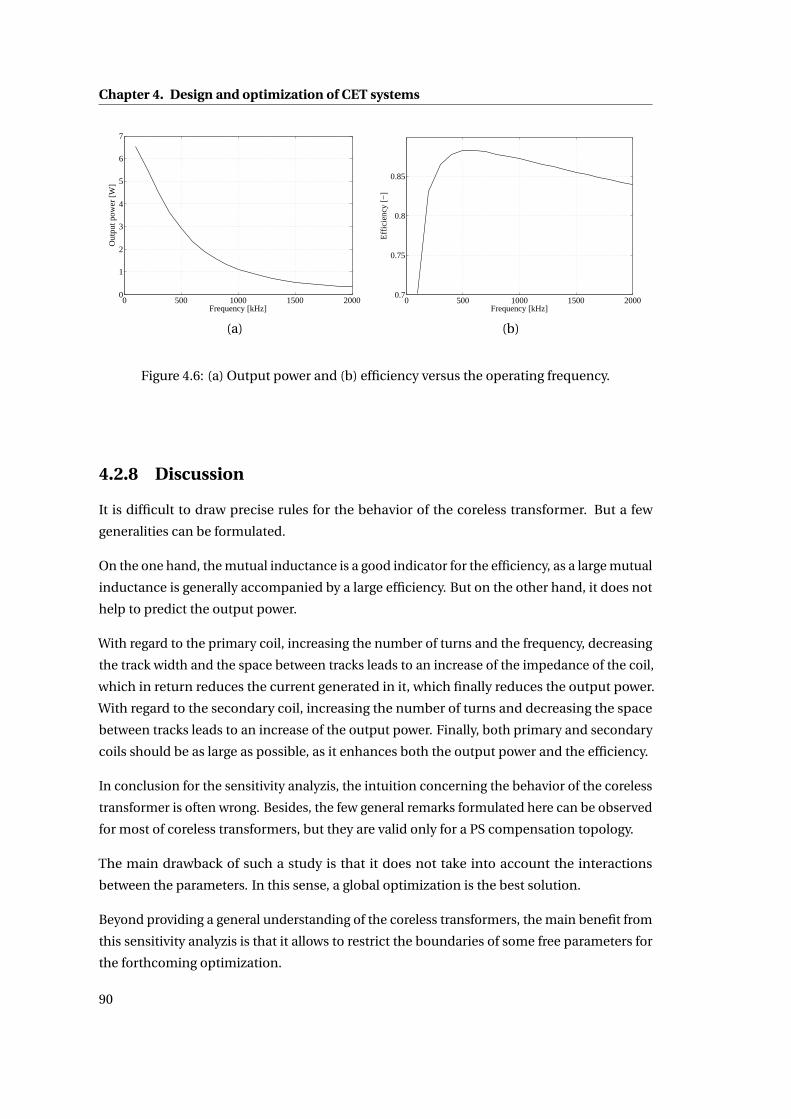
Chapter 4. Design and optimization of CET systems
0 500 1000 1500 20000
1
2
3
4
5
6
7
Frequency [kHz]
Out
put p
ower
[W
]
0 500 1000 1500 20000.7
0.75
0.8
0.85
Frequency [kHz]
Effi
cien
cy [−
]
(a) (b)
Figure 4.6: (a) Output power and (b) efficiency versus the operating frequency.
4.2.8 Discussion
It is difficult to draw precise rules for the behavior of the coreless transformer. But a few
generalities can be formulated.
On the one hand, the mutual inductance is a good indicator for the efficiency, as a large mutual
inductance is generally accompanied by a large efficiency. But on the other hand, it does not
help to predict the output power.
With regard to the primary coil, increasing the number of turns and the frequency, decreasing
the track width and the space between tracks leads to an increase of the impedance of the coil,
which in return reduces the current generated in it, which finally reduces the output power.
With regard to the secondary coil, increasing the number of turns and decreasing the space
between tracks leads to an increase of the output power. Finally, both primary and secondary
coils should be as large as possible, as it enhances both the output power and the efficiency.
In conclusion for the sensitivity analyzis, the intuition concerning the behavior of the coreless
transformer is often wrong. Besides, the few general remarks formulated here can be observed
for most of coreless transformers, but they are valid only for a PS compensation topology.
The main drawback of such a study is that it does not take into account the interactions
between the parameters. In this sense, a global optimization is the best solution.
Beyond providing a general understanding of the coreless transformers, the main benefit from
this sensitivity analyzis is that it allows to restrict the boundaries of some free parameters for
the forthcoming optimization.
90

4.3. Optimization methods
4.3 Optimization methods
Many optimization methods do exist for finding the best solution to a problem issued from
engineering design. As a preliminary introduction to the optimization methods, the different
terms used in the following sections are defined as follows:
• Objective function: Function to be minimized or maximized
• Free parameters: Factors that have an influence on the objective function
• Search space: Domain in which the objective function can be evaluated
• Constraint: Condition that restricts the search space to admissible solutions
• Admissible space: Region of the search space where all constraints are respected
The most obvious method for finding an optimum consists in evaluating all the possible
solutions of a given problem. This is actually the only solution which allows to say with
certainty that the global optimum is reached. But its computation cost is generally huge and
increases greatly with the number of free parameters. Indeed, for problems involving many
parameters (i.e. 10 or more) such as the CET systems studied in this thesis, this method is
clearly not an option.
Besides, there are two kinds of optimization algorithms, the deterministic and the stochastic
algorithms [100].
A deterministic algorithm is an algorithm that behaves in a predictable and repeatable way.
Given a certain function to be maximized or minimized, it will produce at each execution the
same result and will pass through the same algorithm sequences. In other words, deterministic
algorithms produce a solution that is highly dependent on the initial conditions. The most
used and probably most efficient deterministic method is the gradient-based algorithm, in
which the partial derivations of the function to optimize are computed in order to reach a
local optimum where the gradient of the function is zero. The main problem for this kind of
strategy is that there is no way to certify that the resulting solution is a global optimum and not
a local one. The designer has to try multiple initial conditions to increase the chances to reach
the global optimum. Moreover, this method is well suited for problems having an analytical
solution that is stable and differentiable. But the modeling of CET systems includes discrete
parameters (such as the number of turns and the number of layers), and uses numerical
solutions where the analytical solution does not exist (for example the inductance calculation).
For all these reasons, deterministic algorithms such as the gradient method are discarded
from the possible optimization methods in this thesis.
91

Chapter 4. Design and optimization of CET systems
The stochastic methods use randomly generated parameters within their variation range.
Thus, each separate execution of a stochastic algorithm evaluates different solutions. The
problem of global or local convergence does not exist anymore, even if it remains difficult to
prove that a local or global optimum is reached. A stochastic algorithm has greater chances of
converging to the global optimum if the number of iterations or objective function evaluations
is large. Furthermore, it is possible to solve problems involving discrete parameters and non-
differentiable functions. Many stochastic algorithms exist, such as the simulated annealing,
the ant colony optimization or the genetic algorithms. The only one studied in this thesis
is the genetic algorithms (GA) for two reasons. First, it is the most intuitive and convenient.
Secondly, the research group in which this thesis work has been realized has a good experience
of GAs and has already developed a few efficient algorithms [99], [98], [106], [30], [85], [84].
4.4 Genetic algorithms
4.4.1 Generalities
Historically, the first GA was proposed by John Holland in 1975 [64]. But GAs became popu-
larized later in 1989, after David Goldberg published his book [59]. GAs belong to the larger
class of evolutionary algorithms (EA). The main concept is based on the simple principle that
if the evolution has been able to optimize natural biological processes, it can be used as a
paradigm to find optimal solutions to any other problems. Then, GAs take their inspiration on
the natural evolution as in Darwin’s theory, in which the selection, the reproduction, and the
exchange of genes play a central role.
In a GA, a population of individuals is generated. After their evaluation, a few of them (the
best ones according to the law of the survival of the fittest) are selected as parents in order to
generate the next generation. During the process, their genetic material can be exchanged
or undergo different mutations. Over successive generations, the population is supposed to
evolve towards an optimal solution.
In this section, only the main concepts involved in GAs are mentioned so as to make the
future developments coherent and understandable to the reader. More details are presented
in appendix C.1, and multiple references may complete those descriptions [98], [95], [111],
[70].
The specific rules that govern GAs are often called operators. They are responsible for the
definition of the processes that lead to the creation of the new generations and determine how
they replace the former ones. They are generally 5 for conventional GAs:
92

4.4. Genetic algorithms
• The evaluation of individuals: During this phase, each individual is evaluated and
qualitatively quantified in anticipation for the patents selection.
• The selection of the parents: The selection phase consists in generating a new popula-
tion of parents. They are chosen on the basis of the evaluation through an appropriate
method.
• The crossover: The crossover is an operation that allows to exchange the genetic mate-
rial of the parents so as to create one or multiple children.
• The mutation: The mutation is a phase in which random modifications are applied to
the children.
• The replacement: The replacement strategy defines how the children are inserted into
the next generation and therefore how they replace the parents.
A scheme of the working of usual GAs is presented in Fig, 4.7. A description of the different
operators and their implementation is given in appendix C.1.
Randomly createinitial population
Evaluatepopulation
SelectParents
Crossoveroperator
Mutationoperator
Reproduction process
Evaluatechildren
ReplacementoperatorStop ?
Retrieve bestindividuals
yes
no
Figure 4.7: Schematic description of a conventional GA.
4.4.2 Genetic algorithm implementation
As a first attempt, the function ga.m from Matlab optimization toolbox [21] was tested, but the
probabilities of mutation and crossover were difficult to adjust and the management of the
constraints was not compatible with the ones associated with CET applications. Therefore,
[106] and [98] have developed their own GA by including to it three main improvements.
93
Chapter 4. Design and optimization of CET systems
The first improvement is related to the mutation and crossover operators. It consists of the
adaptation of a method proposed in [128] that allows to regulate automatically the crossover
and mutation probabilities according to the population diversity. At the beginning, a great
diversity is imposed so as to ensure a good exploration of the search space. The diversity is
then progressively decreased and oriented towards a local search at the end. As a result, the
searchability of the GA is increased.
The second improvement concerns the crossover operator. It is adapted from [72] and consists
of a specific arithmetic crossover applied to three parents instead of two parents. According to
[72], this crossover increases the convergence speed and in the same time avoids a premature
convergence.
The third improvement concerns the introduction of a local search in the GA. It is based on
[72] and consists in exploring the neighbourhood of the best children at each generation.
Basically, if a so generated individual is better than its original child, it takes his place in the
next generation. This method increases the convergence speed and maintains the diversity in
each generation. In return, it requires some computation time, since the objective functions
of the new individuals have to be evaluated.
4.4.3 Genetic algorithm testing
This last GA has proven to be very effective and has allowed to optimize the design of a surgical
ultrasonic transducer in [98] and a linear actuator in [84]. However, the former involves 11
free parameters and no constraint. The latter involves 4 free parameters and 2 constraints. For
the optimization of CET systems using PCB coils, there are at least 10 free parameters and two
geometrical constraints defined by (3.30). The problem to be solved is then obviously more
complicated. Furthermore, as previously mentioned, two objectives are to be optimized for
CET systems, namely the losses (to be minimized) and the output power (to be maximized). It
is then interesting to test the GA with a simple CET application before to investigate the more
complicated design of the CET table.
In order to test the GA for CET systems, a simple application (called Prob1) is created. It
consists of a simple coreless transformer made up of two well-aligned coils. The goal is to
transfer a power of 5 Watts to a load of 10 Ω, and the maximal size of the coils was fixed to
50 by 50 mm2. These specifications are rather general and could refer to a typical application
such as recharging a portable phone. Prob1 makes a good candidate for testing the GA
presented above. In this simple case, the compensation topology is parallel-series (PS) and
the geometry of the coils is reduced to square and single-layered ones. The input voltage is set
94
4.4. Genetic algorithms
to 12 V (AC rms). With this, the parameters limits (LU) are:
100 < f < 500 [kH z] (4.4)
1 < n1, n2 < 50 [−] (4.5)
20.0 < a1, a2 < 50.0 [mm] (4.6)
0.2 < w1, w2 < 2.0 [mm] (4.7)
0.2 < d1, d2 < 1.5 [mm] (4.8)
In most cases, it is sufficient to optimize only one of two objectives and set the other one as a
constraint. In a first optimization attempt, the objective function to be minimized is chosen
to be the power losses, and the output power is defined as a constraint. The power losses Ploss
generated in the coreless transformer are defined as follows:
Ploss = P j 1 +P j 2 (4.9)
with P j 1 and P j 2 the Joule losses of the primary and secondary coils.
The inequality constraints are defined as follows:
n1(w1 +d1)+ cst < a1
2(4.10)
n2(w2 +d2)+ cst < a2
2(4.11)
Pout > 5 (4.12)
Prob1 has been submitted to the GA and led to bad results because the GA failed to con-
verge properly. The reason comes from the fact that the problem to be solved is too much
constrained. Indeed, the three constraints prevented the GA from converging adequately.
Therefore, to solve this problem, the GA has been applied to another objective function that
allows to eliminate the last constraint.
According to [81], a simple solution to deal with multiobjective problems consists in expressing
a single objective function in the form of a weighted summation, as follows:
O =αPl oss − (1−α)PL (4.13)
where O is the new objective function to be minimized. The term of the output power and the
losses are weighted by a factor α that allows to assign a degree of importance to both criteria.
This parameter has to be fixed according to the application to develop, and theoretically, each
95
Chapter 4. Design and optimization of CET systems
different value of α could lead to a different solution. One can note here that maximizing the
efficiency would be equivalent to minimizing (4.13) for a single and specific value of α.
The GA has been run to optimize Prob1 with this new objective function. Unlike in the preced-
ing attempt, there is no more problems of convergence, but the results remain unsatisfactory.
The reason is that it is impossible to find the right value for α that corresponds exactly to the
specifications. To illustrate this problem, two runs of optimizations are executed for different
values of α. The results are presented in Fig. 4.8.
In the first run, α takes the successive values:
α= 0.89, 0.90, 0.91, . . . , 0.98 (4.14)
With this, a linear relation between the losses and the output power can be observed, but the
spacing between each solution that corresponds to different values of α is too large to obtain
a satisfactory solution. Therefore the variation range for α is refined in the second run, as
follows:
α= 0.9110, 0.9115, 0.9120, . . . , 0.9195 (4.15)
All solutions are also situated on the vicinity of the same straight line as before, but it is
impossible to extract a solution that corresponds to the desired specifications. The set of
solutions undergoes some fluctuations along the straight line when the spacing between
the different values of α is reduced. This can be observed in Fig. 4.9, where the output
power versus α is plotted. The best solution, that is the closest one to the fulfilment of the
specifications of Prob1, would provide an output power of 6.08 W and generate power losses of
0.53 W. This solution is obtained with α= 0.9170. It is not bad in itself, but it is far from being
optimal according to the specifications of Prob1. Indeed, the desired output power is 5 W, and
a solution that is able to provide 6.08 W is sure to generate more Joule losses than one that
would be closer to 5 W. In this sense it is not optimal.
Other solutions have been tried to minimize (4.13). For example, many attempts to assign
different weighting factors and to vary them separately have been carried out, but with similar
unsatisfactory results. Therefore, a new GA has to be implemented, that allows to provide at
least one good solution. So far, a multiobjective problem was reduced to a single-objective
one so as to find its optimum. In the following section, an optimization method that exploits
simultaneously two objective functions is introduced and developed.
96
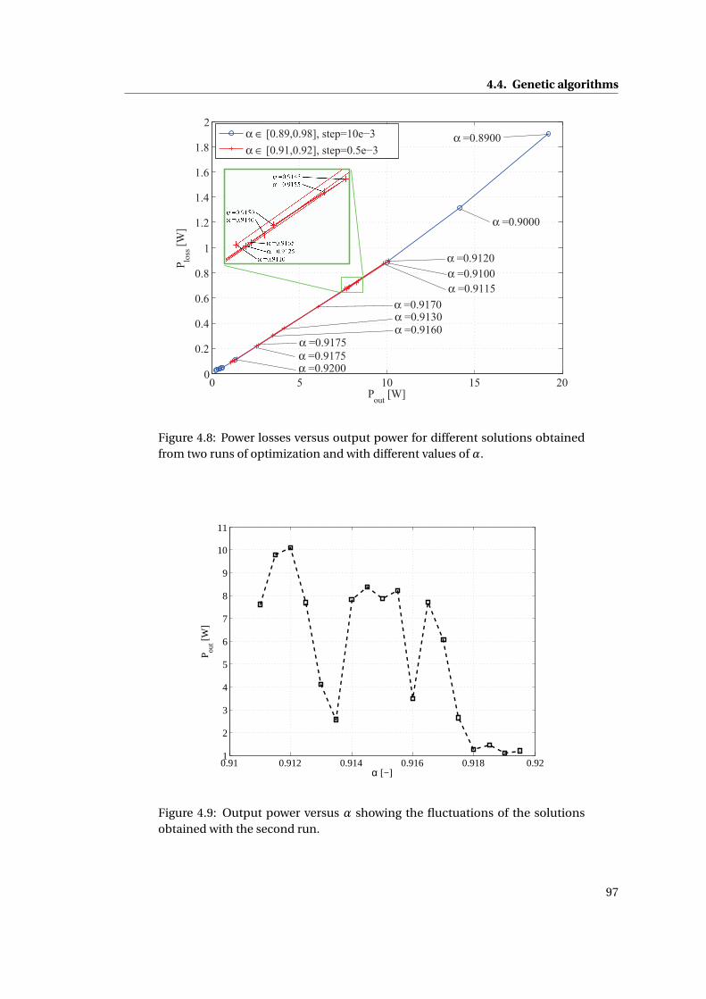
4.4. Genetic algorithms
0 5 10 15 200
0.2
0.4
0.6
0.8
1
1.2
1.4
1.6
1.8
2
Pout [W]
P loss
[W]
α ∈ [0.89,0.98], step=10e−3α ∈ [0.91,0.92], step=0.5e−3
α =0.9115
α =0.9120
α =0.8900
α =0.9000
α =0.9100
α =0.9130α =0.9170
α =0.9160
α =0.9200
α =0.9175α =0.9175
Figure 4.8: Power losses versus output power for different solutions obtainedfrom two runs of optimization and with different values of α.
0.91 0.912 0.914 0.916 0.918 0.921
2
3
4
5
6
7
8
9
10
11
α [−]
P out [W
]
Figure 4.9: Output power versus α showing the fluctuations of the solutionsobtained with the second run.
97

Chapter 4. Design and optimization of CET systems
4.5 Multiobjective genetic algorithms
4.5.1 Pareto optimality
Before entering multiobjective optimization considerations, it is necessary to define the
concept of Pareto optimality. Vilfredo Pareto (1848-1923) was a sociologist and economist
who developed several theories on the study of income distribution and in the analyzis of
individual’s choices. He was the one who first introduced a notion of optimality that consists in
defining an optimum as an individual’s state (of welfare for instance) that cannot be improved
without making at least another individual’s state worse off [23].
In the field of multiobjective minimization, a solution is a Pareto optimum if there is no other
solution that allows to decrease an objective without increasing another one. To illustrate
this, the example of two objectives to be minimized is often used. The concepts of Pareto
domination and Pareto optimum are depicted in Fig. 4.10.
A B
FD
E
Pareto Optimum
Objective 1
Obj
ectiv
e2
Figure 4.10: Explanation of the Pareto optimality. Here, the point D dominatesthe points E and F, because its two objectives are better. A and B belong to the setof Pareto optima, because no other solution dominates them.
Multiple algorithms, in which the Pareto optimality is used, do exist. Some are based on the
simulated annealing method. One can mention for example the PASA (Pareto archived simu-
lated annealing) or MOSA (Multiobjective simulated annealing) methods that are frequently
presented in literature [121], [28]. In this section, the focus is made on the multiobjective
genetic algorithms (MOGAs).
98

4.5. Multiobjective genetic algorithms
4.5.2 Generalities
The organization and the general concepts of the single objective GAs presented in the previous
section remain valid for MOGAs, except for a few differences that will be explained further. The
MOGA provided with the Matlab toolbox has been tried, with the same conclusion as in the
previous section, especially the management of constraints that allows to define only linear
constraints in the search space, which is not sufficient for the optimization of CET systems.
Thus a new MOGA has to be implemented.
There are many kinds of MOGAs, but the most recent and popular ones are the strength
Pareto evolutionary algorithm (SPEA, [133]), the Pareto-archived evolution strategy (PAES,
[74]), and the non-dominated sorting genetic algorithm (NSGA, [116]). The common point to
all these MOGAs is that they integrate the concept of Pareto domination in the evaluation of
the individuals. In this thesis, the developed MOGA is based on the NSGA-II, which is an im-
provement of the NSGA, created so as to respond to the main criticism that was formulated by
the scientific community. This algorithm has been chosen essentially because of its relatively
simple implementation and because it is currently one of the most efficient [41].
Compared to single objective GAs, the main difference with MOGAs comes from the strategy
to maintain the diversity inside the population and to keep a high convergence pressure so
as to obtain a set of solutions that are well spread and uniformly spaced. In the NSGA-II, the
convergence pressure is assured by the elitism operator, which defines how the individuals are
evaluated and then selected inside a population. The diversity is maintained with the niche
operator, which prevents the crowding of solutions in a region of the search space.
With the NSGA-II, there are thus two new operators:
• The elitism operator: It consists of a process that evaluates the individuals of a popu-
lation based on their degree of non-domination. The elitism is also influenced by the
replacement strategy and the niche operator.
• The niche operator: This method allows to limit the number of similar individuals that
are passed to the next generation. In other words, it defines the ability of a MOGA to
spread properly the individuals along the set of Pareto optimal solutions.
The different phases of the MOGA implemented in this thesis (called NSGAimp) are depicted in
Fig. 4.11. Therein, Np is the number of parents, Nc the number of children, and Ntot the total
number of individuals inside the population. Typical values are given for those parameters.
The differences with the single objective GA and the main improvements carried out on the
NSGA-II are described in the following subsections.
99
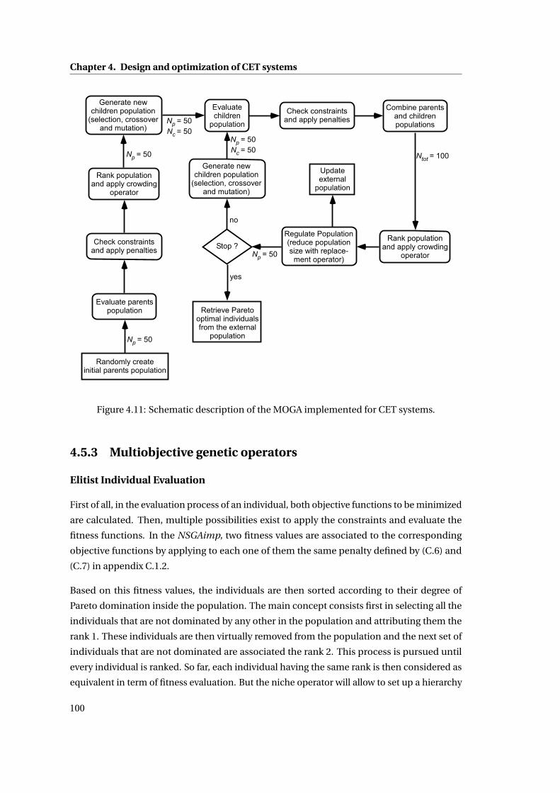
Chapter 4. Design and optimization of CET systems
Randomly createinitial parents population
Evaluate parentspopulation
Check constraintsand apply penalties
Rank populationand apply crowding
operator
Generate newchildren population
(selection, crossoverand mutation)
Evaluatechildren
population
Check constraintsand apply penalties
Combine parentsand childrenpopulations
Rank populationand apply crowding
operator
Regulate Population(reduce populationsize with replace-
ment operator)
Stop ?
yes
no
Generate newchildren population
(selection, crossoverand mutation)
Updateexternal
population
Retrieve Paretooptimal individualsfrom the external
populationNp = 50
Np = 50
Np = 50Nc = 50
Ntot = 100
Np = 50
Np = 50Nc = 50
Figure 4.11: Schematic description of the MOGA implemented for CET systems.
4.5.3 Multiobjective genetic operators
Elitist Individual Evaluation
First of all, in the evaluation process of an individual, both objective functions to be minimized
are calculated. Then, multiple possibilities exist to apply the constraints and evaluate the
fitness functions. In the NSGAimp, two fitness values are associated to the corresponding
objective functions by applying to each one of them the same penalty defined by (C.6) and
(C.7) in appendix C.1.2.
Based on this fitness values, the individuals are then sorted according to their degree of
Pareto domination inside the population. The main concept consists first in selecting all the
individuals that are not dominated by any other in the population and attributing them the
rank 1. These individuals are then virtually removed from the population and the next set of
individuals that are not dominated are associated the rank 2. This process is pursued until
every individual is ranked. So far, each individual having the same rank is then considered as
equivalent in term of fitness evaluation. But the niche operator will allow to set up a hierarchy
100
4.5. Multiobjective genetic algorithms
of each individual belonging to the same rank.
This ranking procedure together with the constraints management that involves the penalty
applied to both objective functions gives a property to the MOGA that is interesting: the
convergence towards feasible solutions in the early generations when there are potentially no
feasible solutions. Especially for CET systems optimization, the constraints are very coercive
and this is the reason why the single objective GA did not work. Here, the ranking procedure is
also applied to individuals that do not satisfy the constraints, and an individual that violates
’less severely’ a constraint than another one is sure to be assigned a lower rank in the popula-
tion. Thanks to that, if there is no feasible solution at early generations, the MOGA evolves
towards the admissible space, and once it is reached, it evolves towards the Pareto optimal set
of solutions.
Niche operator
Niche is a term issued from ecology that describes the relational position of a population (or
multiple species) in its ecosystem. Each species has its own characteristics and occupies a
different niche. In MOGAs, this concept is reused to prevent the algorithm from converging to
a single region of the search space. Among the niching methods, there is the fitness sharing
[116], the crowding method [102], and the clearing procedure [96].
The fitness sharing consists in assigning to each individual a shared fitness that is equal to its
raw fitness divided by a value defined by the number of similar individuals. The greater the
number of similar individuals, the larger is this value. Thus, an isolated individual has a higher
probability to generate offsprings. There are two main problems with this method. First, a
large population should be used so as to reduce the risk of disappearance of subpopulations
during the stochastic evolution of the algorithm. Secondly, this method requires additional
parameters, such as the size of the niche.
The crowding method inserts the children in the population by replacing similar elements. To
do so, the selection process is designed in a way that only couples of similar parents can be
chosen to generate children that will then belong to the same niche. Another possibility is for
the children to replace the individuals that are most similar to them in the population. This
avoids the concentration of all individuals in a single niche.
The clearing procedure is similar to the fitness sharing, except that a maximal number of
individuals per niche is decided, and the fitness is deteriorated only for individuals that exceed
this number. For example, if each niche accepts k individuals, the clearing procedure preserves
the fitness of the k best individuals and decreases the fitness of the other ones that belong
to the same niche. The disadvantage of this method is that it requires additional parameters
101
Chapter 4. Design and optimization of CET systems
(size of the niche, number of niches, maximal number of individuals per niche).
In the NSGAimp, the diversity is preserved using a crowded-distance approach similar to the
one proposed in [48]. The crowded distance consists of an estimation of the density of the
individuals surrounding the one that is evaluated. It is determined by summing the distance
of the two individuals situated on either sides of the evaluated individual (in the objective
space). This distance is then normalized to the extreme values of objective functions obtained
in the population. In other words, a smaller crowded distance is assigned to individuals that
are more crowded. All individuals of the population are given a crowded distance according to
their rank. This method has the advantage not to require additional parameters. In brief, each
individual is characterized by two values: its rank and its crowded distance.
Elitist replacement strategy
In a wide sense, an elitist strategy consists in preserving the best individuals from one genera-
tion to another. For MOGAs, it means that each individual belonging to the first rank have to
be transfered to the next generation. This is easily performed during the first generations, for
which the number of first rank solutions is smaller than the size of the children population. At
an advanced stage of the MOGA, the population formed by parents and children may count
more first ranked individuals than can be passed to the next generation. Here, the crowding
operator comes into play and selects the individuals that are most isolated.
Thus, the replacement strategy applied to the MOGA developed in this thesis consists in
selecting primarily the individuals belonging to the lowest ranks and secondarily the ones that
are less crowded.
4.5.4 Multiobjective genetic algorithm implementation
The different phases of the MOGA implemented to optimize CET systems are shown in Fig.
4.11. In addition to the strategy that ensures the convergence towards feasible solutions at
early generations, three main improvements are applied to the MOGA. These are probably our
main contributions to the development of an efficient MOGA.
The first improvement is related to a new strategy that combines the strengths of two different
crossover methods. First, a standard uniform crossover offers a good convergence pressure
but limits the diversity of the population because the original parameters of the parents are
transferred to the children. This results in a quick convergence at early generations, but
a slower one when the algorithm becomes close to the optimal set of solutions. Secondly,
the arithmetic crossover introduced in section 4.4.2, involving three parents to generate
102

4.5. Multiobjective genetic algorithms
two children, has a relatively low convergence pressure but allows to spread considerably
the individuals in the search space, resulting in an excellent diversity inside the population.
NSGAimp cumulates both advantages by using alternatively those two crossovers. Doing so
improves the overall speed of convergence and introduces more diversity in the population.
The second improvement is based on [108]. The MOGA developed therein includes an exter-
nal file that contains the optimal solutions of each generation. This file is updated at each
generation and only the first ranked solutions are kept. In the NSGAimp, this idea is reused by
updating at each generation an external population that contains all the optimal solutions.
All individuals assigned to rank 1 at each generation are registered in the external population.
Within this external population, the dominated individuals are removed. If the number of
individuals in the external population is greater than its maximal admissible number Nmax ,
the most similar individuals are removed using the crowded distance operator. The external
population does not interfere in the MOGA, it is just a passive tool that prevents the loss of
optimal solutions during the elitist evolution of the MOGA.
The third improvement concerns the mutation operator. The mutation operator developed
for the NSGAimp involves a polynomial probability distribution Pp as described in [40], a
multiplication coefficient c and the current value of the parameters Xi . The mutated value of
a parameter is then calculated as follows:
Xi ,mut ated = Xi + cPp Xi (4.16)
The polynomial probability distribution is defined so that −1 < Pp < 1 and Pp has a larger
probability to be in the vicinity of zero. For more details, the reader should refer to [40]. The
multiplication coefficient c is dynamically varied during the evolution of the MOGA. Thus, c
has been empirically defined so that, at generation k, it is given by:
c =(20 · (25 ·10−3)
(1− k
T
)0.5)−1(4.17)
with T the maximal number of generations. To show the effect of the coefficient c, as an
example, the maximal number of generations is set to T = 500. The resulting value of c is
shown in Fig. 4.12. This dynamical variation of c introduces an aggressive strategy of mutations
at early generations and reduces progressively the mutation values so as to obtain very small
perturbations at the end of the MOGA.
4.5.5 MOGA testing
Different test functions are frequently used to evaluate the MOGAs. Zitzler et al., a reference
in the world of MOGAs, proposed six unconstrained test functions in [132]. The first four of
103

Chapter 4. Design and optimization of CET systems
0 100 200 300 400 5000
0.5
1
1.5
2
Generation k
Coe
ffic
ient
c
Figure 4.12: Multiplication coefficient evolution.
these six problems will be used in this section and are called ZDT1, ZDT2, ZDT3, and ZDT4.
In addition, two constrained problems, called Constr [41] and Tnk [122] are tested. All these
test functions are defined in detail and their Pareto front plotted in appendix C.2. Finally, the
MOGA will be tested on Prob1 that has been defined in section 4.4.3.
In all problems, the population size is set to Ntot = 100 individuals, in which Nc = 50 children
are generated at each iteration. The number of generations is set to T = 120 which leads to a
total of 6000 function evaluations, which is relatively low to reach an acceptable convergence
for many problems. Each function is tested with the NSGAimp and the NSGA-II provided in
the Matlab toolbox in order to compare their performance, except the Tnk function for which
it is impossible because of the second order constraints.
For all unconstrained test functions, the worst, best and average results obtained over 15 runs
are presented in Fig. 4.13. The number of parameters is set to 15 for ZDT1, ZDT2, ZDT3, and to
10 for ZDT4. The results show that NSGAimp is much more efficient in terms of convergence
and number of Pareto solutions. Furthermore, each run provides similar results with NSGAimp,
which is a guarantee of stability and repetitiveness.
For the constrained problems Constr and Tnk, equivalent results are obtained from different
runs. Therefore, Fig. 4.14 shows the results of only single runs. The results show that for Constr,
the convergence is equivalent for NSGAimp and Matlab’s NSGA-II. However, the number of
optimal solutions is greater for the former which makes it more interesting. Results on Tnk
show that NSGAimp is able to handle effectively second order constraints.
Finally, NSGAimp is tested on the problem Prob1. The two objective functions to be optimized
104
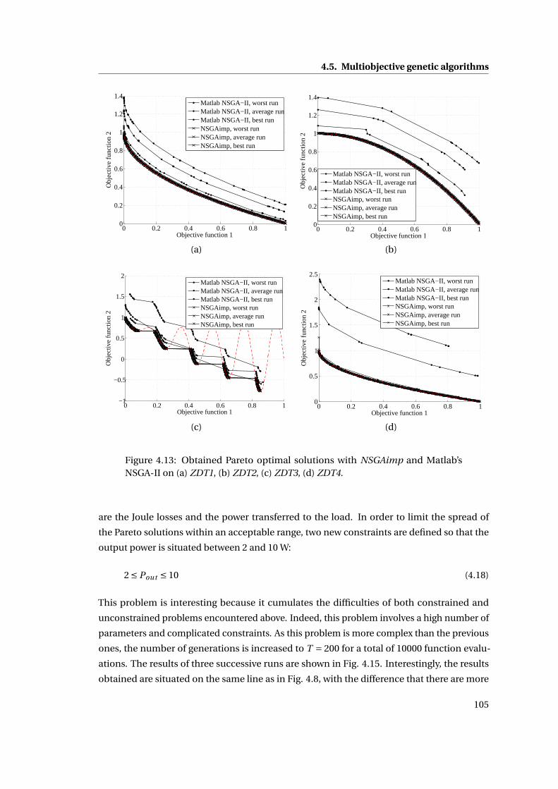
4.5. Multiobjective genetic algorithms
0 0.2 0.4 0.6 0.8 10
0.2
0.4
0.6
0.8
1
1.2
1.4
Objective function 1
Obj
ectiv
e fu
nctio
n 2
Matlab NSGA−II, worst runMatlab NSGA−II, average runMatlab NSGA−II, best runNSGAimp, worst runNSGAimp, average runNSGAimp, best run
0 0.2 0.4 0.6 0.8 10
0.2
0.4
0.6
0.8
1
1.2
1.4
Objective function 1
Obj
ectiv
e fu
nctio
n 2
Matlab NSGA−II, worst runMatlab NSGA−II, average runMatlab NSGA−II, best runNSGAimp, worst runNSGAimp, average runNSGAimp, best run
(a) (b)
0 0.2 0.4 0.6 0.8 1−1
−0.5
0
0.5
1
1.5
2
Objective function 1
Obj
ectiv
e fu
nctio
n 2
Matlab NSGA−II, worst runMatlab NSGA−II, average runMatlab NSGA−II, best runNSGAimp, worst runNSGAimp, average runNSGAimp, best run
0 0.2 0.4 0.6 0.8 10
0.5
1
1.5
2
2.5
Objective function 1
Obj
ectiv
e fu
nctio
n 2
Matlab NSGA−II, worst runMatlab NSGA−II, average runMatlab NSGA−II, best runNSGAimp, worst runNSGAimp, average runNSGAimp, best run
(c) (d)
Figure 4.13: Obtained Pareto optimal solutions with NSGAimp and Matlab’sNSGA-II on (a) ZDT1, (b) ZDT2, (c) ZDT3, (d) ZDT4.
are the Joule losses and the power transferred to the load. In order to limit the spread of
the Pareto solutions within an acceptable range, two new constraints are defined so that the
output power is situated between 2 and 10 W:
2 ≤ Pout ≤ 10 (4.18)
This problem is interesting because it cumulates the difficulties of both constrained and
unconstrained problems encountered above. Indeed, this problem involves a high number of
parameters and complicated constraints. As this problem is more complex than the previous
ones, the number of generations is increased to T = 200 for a total of 10000 function evalu-
ations. The results of three successive runs are shown in Fig. 4.15. Interestingly, the results
obtained are situated on the same line as in Fig. 4.8, with the difference that there are more
105

Chapter 4. Design and optimization of CET systems
0.3 0.4 0.5 0.6 0.7 0.8 0.9 10
2
4
6
8
10
Objective function 1
Obj
ectiv
e fu
nctio
n 2
Matlab NSGA−IIMatlab NSGAimp
0 0.2 0.4 0.6 0.8 1 1.20
0.2
0.4
0.6
0.8
1
1.2
Objective function 1
Obj
ectiv
e fu
nctio
n 2
NSGAimp
(a) (b)
Figure 4.14: (a) Obtained Pareto optimal solutions with NSGAimp and Matlab’sNSGA-II on Constr. (b) Obtained Pareto optimal solutions with NSGAimp on Tnk.
than 200 available solutions spread along this line for each run. In this case again, NSGAimp
shows a good stability and effectiveness.
2 4 6 8 100
0.2
0.4
0.6
0.8
1
Pout
[W]
P loss
[W
]
NSGAimp, run 1NSGAimp, run 2NSGAimp, run 3
Figure 4.15: Pareto optimal solutions obtained for three successive runs of NS-GAimp on the problem Prob1.
To determine the final solution for an application, one has only to choose the adequate
solution that meets the specifications. For the problem Prob1, the goal is to obtain an output
106

4.6. Design of the CET table
power of 5 W, which is obtained with the set of input parameters given in Table 4.2. The
calculated output power and power losses of the corresponding coreless transformer are given
in Table 4.3. Finally, this solution has been realized and measured using the electronics and
the setup that will be presented in section 5.1.3. The measured values are just mentioned here
so as to compare them with the calculated ones.
Table 4.2: Free parameters.
Primary coil Secondary coil
Parameter Value Parameter Value
n1 9 n2 10a1 49.60 mm a2 50.00 mmw1 1.21 mm w2 0.94 mmd1 0.47 mm d2 0.40 mmf 500 kHz
Table 4.3: Output parameters.
Parameter Calc. value Meas. value
Pout 5.03 W 5.05 WP j 1 0.23 W 0.25 WP j 2 0.21 W 0.22 W
Pl oss 0.44 W 0.47 Wη 92 % 92 %
This validates the use of NSGAimp for simple CET applications. However, for more complicated
CET systems such as the CET table, some preliminary remarks have to be done concerning
the design. Based on the sensitivity analyzis of section 4.2 and the MOGA developed in this
section, a strategy to design the CET table is presented in the following section.
4.6 Design of the CET table
4.6.1 Context and specifications
The goal consists in designing a CET table for multiple low-powered loads. The expectations
for such a CET table can be formulated as follows:
• It must be able to supply simultaneously small peripherals such as a mouse, a keyboard
and a loudspeaker.
107
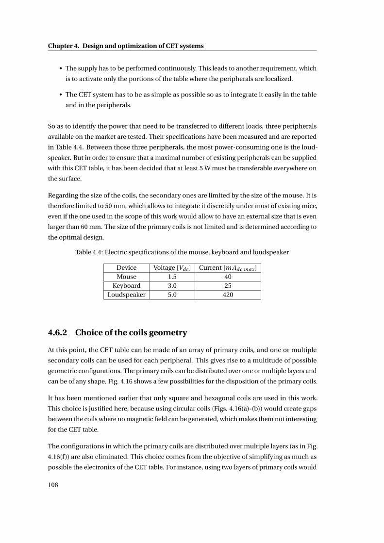
Chapter 4. Design and optimization of CET systems
• The supply has to be performed continuously. This leads to another requirement, which
is to activate only the portions of the table where the peripherals are localized.
• The CET system has to be as simple as possible so as to integrate it easily in the table
and in the peripherals.
So as to identify the power that need to be transferred to different loads, three peripherals
available on the market are tested. Their specifications have been measured and are reported
in Table 4.4. Between those three peripherals, the most power-consuming one is the loud-
speaker. But in order to ensure that a maximal number of existing peripherals can be supplied
with this CET table, it has been decided that at least 5 W must be transferable everywhere on
the surface.
Regarding the size of the coils, the secondary ones are limited by the size of the mouse. It is
therefore limited to 50 mm, which allows to integrate it discretely under most of existing mice,
even if the one used in the scope of this work would allow to have an external size that is even
larger than 60 mm. The size of the primary coils is not limited and is determined according to
the optimal design.
Table 4.4: Electric specifications of the mouse, keyboard and loudspeaker
Device Voltage [Vdc ] Current [m Adc,max ]Mouse 1.5 40
Keyboard 3.0 25Loudspeaker 5.0 420
4.6.2 Choice of the coils geometry
At this point, the CET table can be made of an array of primary coils, and one or multiple
secondary coils can be used for each peripheral. This gives rise to a multitude of possible
geometric configurations. The primary coils can be distributed over one or multiple layers and
can be of any shape. Fig. 4.16 shows a few possibilities for the disposition of the primary coils.
It has been mentioned earlier that only square and hexagonal coils are used in this work.
This choice is justified here, because using circular coils (Figs. 4.16(a)-(b)) would create gaps
between the coils where no magnetic field can be generated, which makes them not interesting
for the CET table.
The configurations in which the primary coils are distributed over multiple layers (as in Fig.
4.16(f)) are also eliminated. This choice comes from the objective of simplifying as much as
possible the electronics of the CET table. For instance, using two layers of primary coils would
108
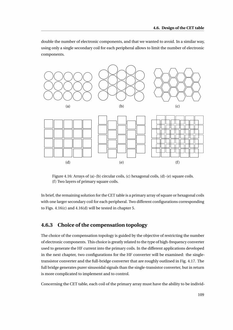
4.6. Design of the CET table
double the number of electronic components, and that we wanted to avoid. In a similar way,
using only a single secondary coil for each peripheral allows to limit the number of electronic
components.
(a) (b) (c)
(d) (e) (f)
Figure 4.16: Arrays of (a)-(b) circular coils, (c) hexagonal coils, (d)-(e) square coils.(f) Two layers of primary square coils.
In brief, the remaining solution for the CET table is a primary array of square or hexagonal coils
with one larger secondary coil for each peripheral. Two different configurations corresponding
to Figs. 4.16(c) and 4.16(d) will be tested in chapter 5.
4.6.3 Choice of the compensation topology
The choice of the compensation topology is guided by the objective of restricting the number
of electronic components. This choice is greatly related to the type of high-frequency converter
used to generate the HF current into the primary coils. In the different applications developed
in the next chapter, two configurations for the HF converter will be examined: the single-
transistor converter and the full-bridge converter that are roughly outlined in Fig. 4.17. The
full bridge generates purer sinusoidal signals than the single-transistor converter, but in return
is more complicated to implement and to control.
Concerning the CET table, each coil of the primary array must have the ability to be individ-
109

Chapter 4. Design and optimization of CET systems
(a) (b)
Figure 4.17: (a) Single-transistor converter. (b) Full-bridge converter
ually activated and deactivated. A large number of switches and electronic components are
therefore required to control the whole CET table. For example, an interesting solution to a
similar application is proposed in [112]. Therein, the electronics used to control a relatively
small CET platform includes three transistors per primary coil, a demultiplexer, a multitude of
drivers and other smaller components. The place it requires is really huge, much larger than
the CET platform itself.
Because it allows to reduce the number of electronic components of the CET table developed
in this thesis, a novel switching configuration based on the single-transistor converter is
proposed. This will be discussed more into details in chapter 5.
To achieve the resonance with the primary inductance, it is necessary to place the primary
compensation capacitor C1 in parallel when using such a single-transistor converter. The
secondary compensation is placed in series, because in this case the reflected impedance is
strictly real and therefore the secondary circuit draws only active power.
4.6.4 CET table Optimization
In brief, the aim is to optimize a CET system composed of an array of primary coils and
larger secondary coils. The losses are to be minimized and a minimal power of 5 W has to be
transferred above the whole surface. The first idea that comes into mind to solve this problem
consists in placing the secondary coil in the position where it is most difficult to reach this
minimal amount of power and performing the optimization for this position. This method
was tested and provided unsatisfactory results because the power was too much fluctuating as
a function of the position of the secondary coil. Moreover, it did not allow to certify that the
minimal power was transferred over the whole surface.
110

4.6. Design of the CET table
Then, the strategy adopted to optimize the CET table consists in separating the problem into
different scenarios. Doing so allows to obtain a smaller fluctuation of the output power over
the surface and ensures that the minimal power is transferred to the load.
For an array of square coils such as the one in Fig. 4.16(d), assuming that the secondary coil
remains parallel to the primary ones, one can consider three different scenarios depicted in
Fig. 4.18:
• The secondary coil is well aligned with a primary one. This corresponds to the position
P1. In this case, only the concerned primary coil has to be activated.
• The secondary coil is placed above two adjacent primary coils. This corresponds to the
position P2. In this case, both concerned primary coils have to be activated.
• The secondary coil is placed above four adjacent primary coils. This corresponds to the
position P3. In this case, the four concerned primary coils have to be activated.
(a) (b) (c)
Figure 4.18: (a) Position P1, (b) position P2, (c) position P3.
Similarly for hexagonal coils, three different scenarios corresponding to positions Pa , Pb ,
Pc , can be considered and are described in Fig. 4.19. Different tests have shown that the
optimization provides better results when the position Pa from the first scenario is laterally
shifted by half the radius of a primary coil.
During the optimization, the three scenarios have to be taken into account. It is done by
summing the respective output powers of each scenario in the first objective function and
summing the respective power losses of each scenario in the second objective function. For
example, applying this to an array of hexagonal coils as shown in Fig. 4.19 leads to the following
objective functions (to be minimized):
O1 = −Pout ,a −Pout ,b −Pout ,c (4.19)
O2 = Ploss,a +Pl oss,b +Ploss,c (4.20)
111
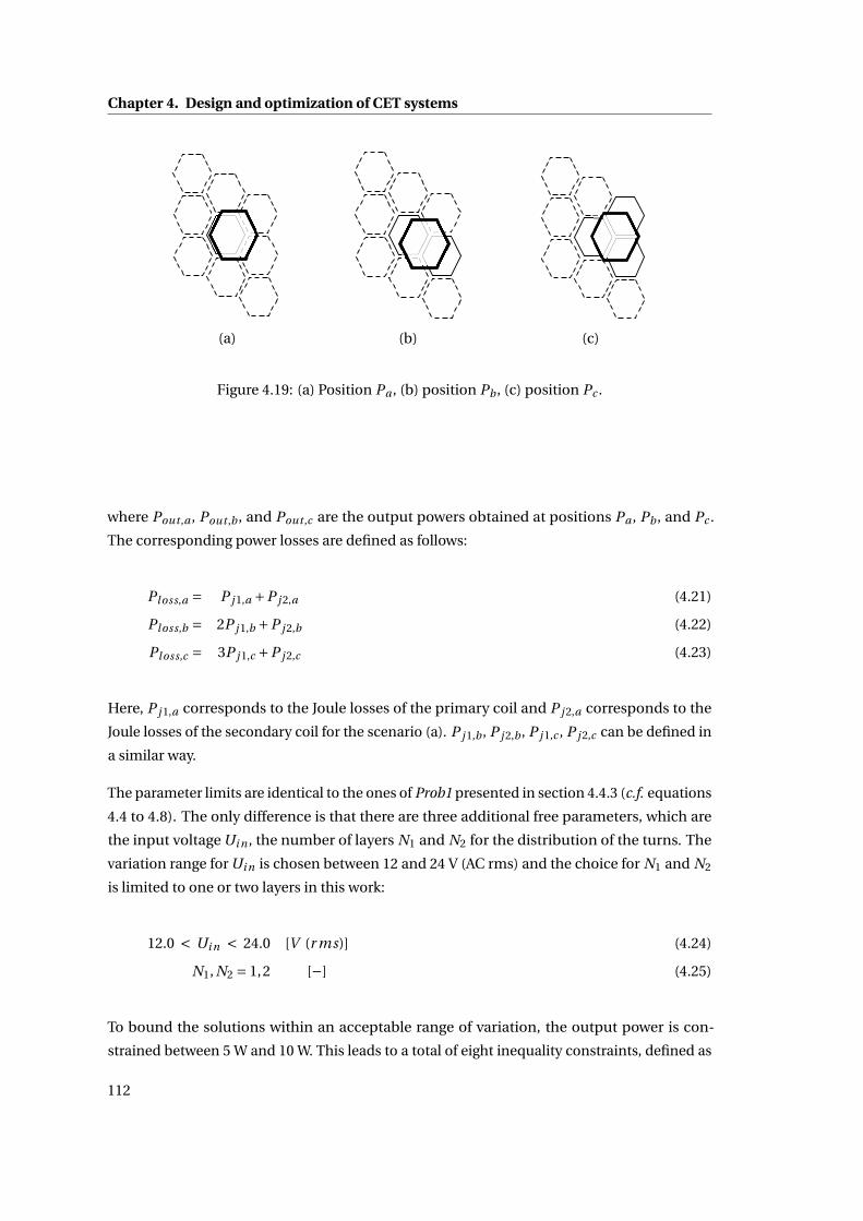
Chapter 4. Design and optimization of CET systems
(a) (b) (c)
Figure 4.19: (a) Position Pa , (b) position Pb , (c) position Pc .
where Pout ,a , Pout ,b , and Pout ,c are the output powers obtained at positions Pa , Pb , and Pc .
The corresponding power losses are defined as follows:
Pl oss,a = P j 1,a +P j 2,a (4.21)
Ploss,b = 2P j 1,b +P j 2,b (4.22)
Ploss,c = 3P j 1,c +P j 2,c (4.23)
Here, P j 1,a corresponds to the Joule losses of the primary coil and P j 2,a corresponds to the
Joule losses of the secondary coil for the scenario (a). P j 1,b , P j 2,b , P j 1,c , P j 2,c can be defined in
a similar way.
The parameter limits are identical to the ones of Prob1 presented in section 4.4.3 (c.f. equations
4.4 to 4.8). The only difference is that there are three additional free parameters, which are
the input voltage Ui n , the number of layers N1 and N2 for the distribution of the turns. The
variation range for Ui n is chosen between 12 and 24 V (AC rms) and the choice for N1 and N2
is limited to one or two layers in this work:
12.0 < Ui n < 24.0 [V (r ms)] (4.24)
N1, N2 = 1,2 [−] (4.25)
To bound the solutions within an acceptable range of variation, the output power is con-
strained between 5 W and 10 W. This leads to a total of eight inequality constraints, defined as
112

4.6. Design of the CET table
follows:
n1
N1(w1 +d1)+ cst < a1
2(4.26)
n2
N2(w2 +d2)+ cst < a2
2(4.27)
Pout ,a < 10 (4.28)
Pout ,b < 10 (4.29)
Pout ,c < 10 (4.30)
Pout ,a > 5 (4.31)
Pout ,b > 5 (4.32)
Pout ,c > 5 (4.33)
As a recall, cst is a parameter that corresponds to the minimal free space inside the coils where
no copper can be present. In this work, it is set to 2 mm.
The NSGAimp is then applied to this problem. As it is much more complicated than the
previously encountered ones, the number of generations is set to T = 400, which gives a total
of 20’000 function evaluations. The results of three consecutive runs are given in Fig. 4.20. In
order to take advantage of the full potential offered by the multi-core computers, the “parallel
computing toolbox” from Matlab has been used. Notably, the function “parfor” allows to
distribute simultaneously different tasks to the four cores (clocked at 2.5 GHz) of the CPU. In
this case, it has reduced the computation time by a factor of 3 to 3.5. As a result, a run typically
requires between 8 and 10 hours of computing time.
As for Prob1, the result of the three runs are similar. Each solution so obtained could fulfill
the specifications. But in this specific case, the goal is to choose one that allows to provide
at least 5 W at every position with the lowest Joule losses and with the lowest fluctuation of
output power. Thus, a judicious choice consists in picking the solution with the lowest total
Joule losses. The set of free parameters for this solution is given in Table 4.5 and the output
parameters are given in Table 4.6. This solution will be experimentally tested in section 5.2.8.
113
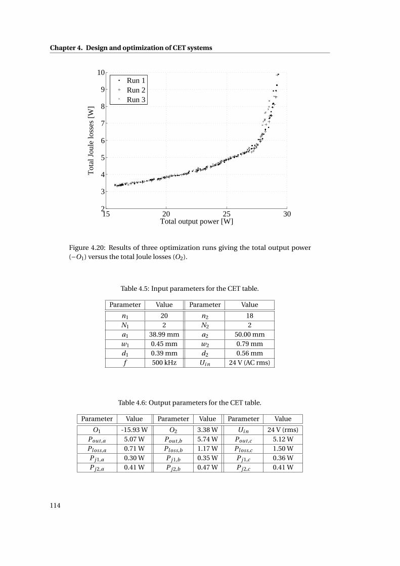
Chapter 4. Design and optimization of CET systems
15 20 25 302
3
4
5
6
7
8
9
10
Total output power [W]
Tot
al J
oule
loss
es [
W]
Run 1Run 2Run 3
Figure 4.20: Results of three optimization runs giving the total output power(−O1) versus the total Joule losses (O2).
Table 4.5: Input parameters for the CET table.
Parameter Value Parameter Value
n1 20 n2 18N1 2 N2 2a1 38.99 mm a2 50.00 mmw1 0.45 mm w2 0.79 mmd1 0.39 mm d2 0.56 mmf 500 kHz Ui n 24 V (AC rms)
Table 4.6: Output parameters for the CET table.
Parameter Value Parameter Value Parameter Value
O1 -15.93 W O2 3.38 W Ui n 24 V (rms)Pout ,a 5.07 W Pout ,b 5.74 W Pout ,c 5.12 WPloss,a 0.71 W Ploss,b 1.17 W Ploss,c 1.50 WP j 1,a 0.30 W P j 1,b 0.35 W P j 1,c 0.36 WP j 2,a 0.41 W P j 2,b 0.47 W P j 2,c 0.41 W
114

4.7. Overall conclusion
4.7 Overall conclusion
In this chapter, a general method to design CET systems is given. First, a sensitivity analyzis is
performed and allows to anticipate the variation range and the impact of the main parameters
on a CET system.
Then, a new MOGA is developed so as to generate an optimal design for different CET systems.
This new MOGA has been tested and has proven to provide excellent results in terms of
convergence and diversity.
The main and innovative contribution of this chapter consists of the establishment of a method
that allows to design and optimize both fixed and movable CET systems. The only difference
resides in the number of scenarios to evaluate. Fixed position systems are designed by taking
into account only a single position evaluation, and free position systems are designed by
considering multiple scenarios for the position of the secondary coil. Thanks to this strategy,
only the two objective functions have to be adapted, but the rest of the design process is left
unchanged.
115

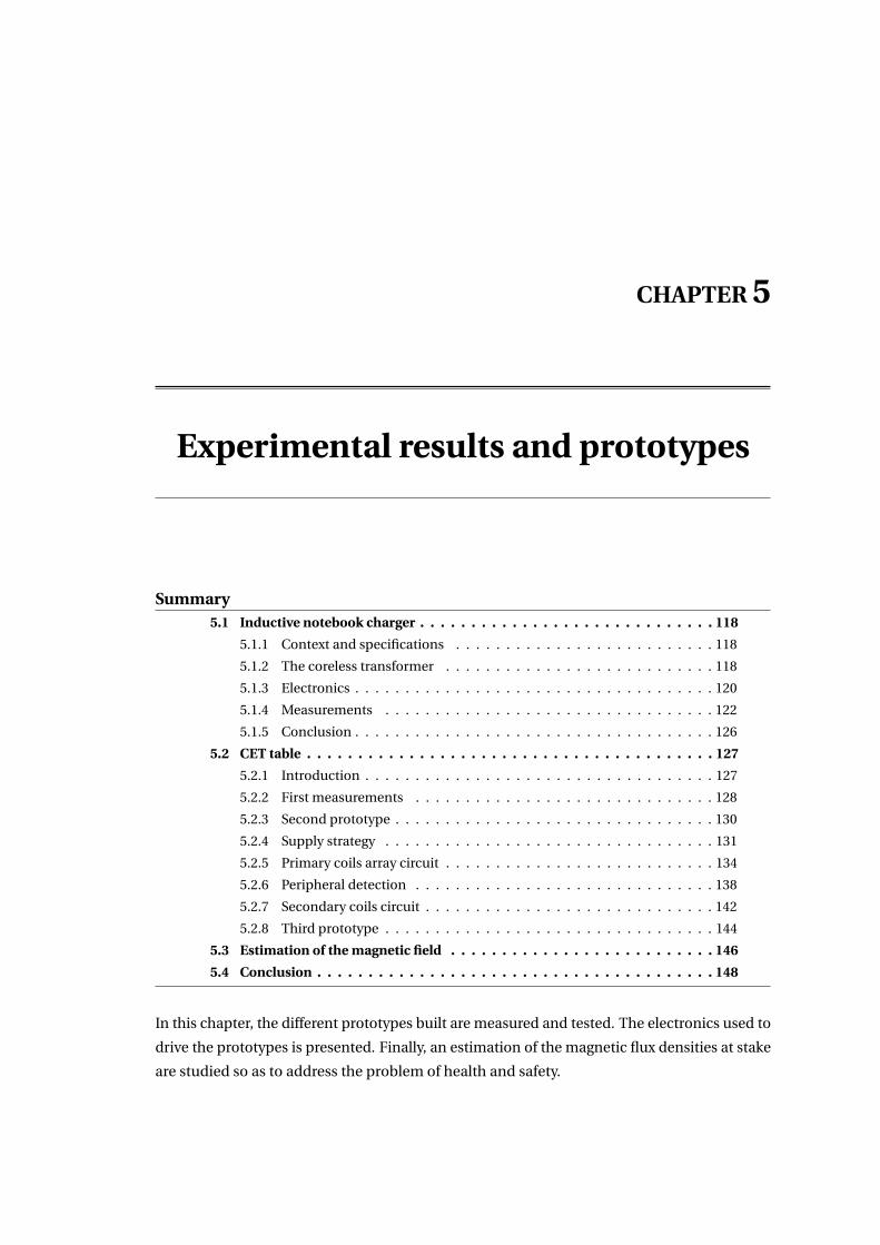
CHAPTER 5
Experimental results and prototypes
Summary5.1 Inductive notebook charger . . . . . . . . . . . . . . . . . . . . . . . . . . . . . 118
5.1.1 Context and specifications . . . . . . . . . . . . . . . . . . . . . . . . . . 118
5.1.2 The coreless transformer . . . . . . . . . . . . . . . . . . . . . . . . . . . 118
5.1.3 Electronics . . . . . . . . . . . . . . . . . . . . . . . . . . . . . . . . . . . . 120
5.1.4 Measurements . . . . . . . . . . . . . . . . . . . . . . . . . . . . . . . . . 122
5.1.5 Conclusion . . . . . . . . . . . . . . . . . . . . . . . . . . . . . . . . . . . . 126
5.2 CET table . . . . . . . . . . . . . . . . . . . . . . . . . . . . . . . . . . . . . . . . 127
5.2.1 Introduction . . . . . . . . . . . . . . . . . . . . . . . . . . . . . . . . . . . 127
5.2.2 First measurements . . . . . . . . . . . . . . . . . . . . . . . . . . . . . . 128
5.2.3 Second prototype . . . . . . . . . . . . . . . . . . . . . . . . . . . . . . . . 130
5.2.4 Supply strategy . . . . . . . . . . . . . . . . . . . . . . . . . . . . . . . . . 131
5.2.5 Primary coils array circuit . . . . . . . . . . . . . . . . . . . . . . . . . . . 134
5.2.6 Peripheral detection . . . . . . . . . . . . . . . . . . . . . . . . . . . . . . 138
5.2.7 Secondary coils circuit . . . . . . . . . . . . . . . . . . . . . . . . . . . . . 142
5.2.8 Third prototype . . . . . . . . . . . . . . . . . . . . . . . . . . . . . . . . . 144
5.3 Estimation of the magnetic field . . . . . . . . . . . . . . . . . . . . . . . . . . 146
5.4 Conclusion . . . . . . . . . . . . . . . . . . . . . . . . . . . . . . . . . . . . . . . 148
In this chapter, the different prototypes built are measured and tested. The electronics used to
drive the prototypes is presented. Finally, an estimation of the magnetic flux densities at stake
are studied so as to address the problem of health and safety.

Chapter 5. Experimental results and prototypes
5.1 Inductive notebook charger
5.1.1 Context and specifications
As mentioned in chapter 1, the aim of this section is to design a CET system from the Alto
platform (depicted in Fig. 1.2) to a notebook charger. To achieve this, Litz wires are used
because the external size of the coils is quite large and because they offer in this case the
best compromise between resistivity and integration. This prototype will allow to validate
experimentally the modeling of coreless transformers presented in chapter 2.
A preliminary study has allowed to establish the specifications of the coreless transformer.
The details of this study are presented in appendix D. A summary of the specifications is given
in Table 5.1. The global electronics schematic of the CET system is presented in Fig. 5.1. It
includes the following main parts (or functions):
• the input rectifier;
• the full-bridge converter;
• the coreless transformer;
• the output rectifier.
Table 5.1: Specifications of the CET notebook charger demonstrator
Specification Description
Maximal coils size 240 mm by 160 mmAirgap 10 mm
Input voltage U1 = 355 V (AC rms)Output voltage U2 = 20 V (AC rms)
Load power PL = 80 W
5.1.2 The coreless transformer
The choice of the compensation topology is based on the specifications. The notebook battery
requires a stable voltage of 20 V (DC) even when the load fluctuates during the charging
process. A good candidate for this specification is the PS topology. This choice will be verified
by measurements.
The used Litz wire has a radius of 1 mm so as to support the current that flows through the coils.
The space between two turns is chosen as small as possible so that each turn is in physical
118
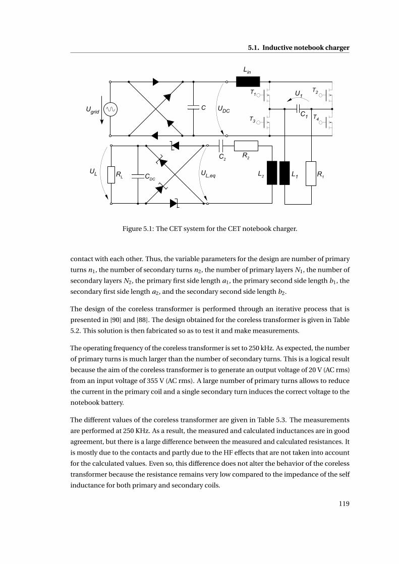
5.1. Inductive notebook charger
T3
UDC C1
L1
U1
CUgrid
Lin
T1T2
T4
L2
R2C2
RL CDC
UL UL,eq R1
Figure 5.1: The CET system for the CET notebook charger.
contact with each other. Thus, the variable parameters for the design are number of primary
turns n1, the number of secondary turns n2, the number of primary layers N1, the number of
secondary layers N2, the primary first side length a1, the primary second side length b1, the
secondary first side length a2, and the secondary second side length b2.
The design of the coreless transformer is performed through an iterative process that is
presented in [90] and [88]. The design obtained for the coreless transformer is given in Table
5.2. This solution is then fabricated so as to test it and make measurements.
The operating frequency of the coreless transformer is set to 250 kHz. As expected, the number
of primary turns is much larger than the number of secondary turns. This is a logical result
because the aim of the coreless transformer is to generate an output voltage of 20 V (AC rms)
from an input voltage of 355 V (AC rms). A large number of primary turns allows to reduce
the current in the primary coil and a single secondary turn induces the correct voltage to the
notebook battery.
The different values of the coreless transformer are given in Table 5.3. The measurements
are performed at 250 KHz. As a result, the measured and calculated inductances are in good
agreement, but there is a large difference between the measured and calculated resistances. It
is mostly due to the contacts and partly due to the HF effects that are not taken into account
for the calculated values. Even so, this difference does not alter the behavior of the coreless
transformer because the resistance remains very low compared to the impedance of the self
inductance for both primary and secondary coils.
119
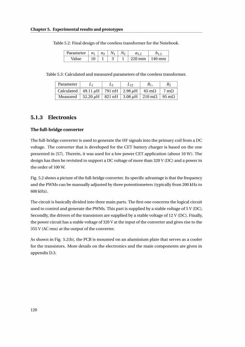
Chapter 5. Experimental results and prototypes
Table 5.2: Final design of the coreless transformer for the Notebook.
Parameter n1 n2 N1 N2 a1,2 b1,2
Value 10 1 3 1 220 mm 140 mm
Table 5.3: Calculated and measured parameters of the coreless transformer.
Parameter L1 L2 L12 R1, R2
Calculated 49.11 µH 791 nH 2.98 µH 65 mΩ 7 mΩMeasured 52.20 µH 821 nH 3.08 µH 210 mΩ 95 mΩ
5.1.3 Electronics
The full-bridge converter
The full-bridge converter is used to generate the HF signals into the primary coil from a DC
voltage. The converter that is developed for the CET battery charger is based on the one
presented in [57]. Therein, it was used for a low power CET application (about 10 W). The
design has then be revisited to support a DC voltage of more than 320 V (DC) and a power in
the order of 100 W.
Fig. 5.2 shows a picture of the full-bridge converter. Its specific advantage is that the frequency
and the PWMs can be manually adjusted by three potentiometers (typically from 200 kHz to
600 kHz).
The circuit is basically divided into three main parts. The first one concerns the logical circuit
used to control and generate the PWMs. This part is supplied by a stable voltage of 5 V (DC).
Secondly, the drivers of the transistors are supplied by a stable voltage of 12 V (DC). Finally,
the power circuit has a stable voltage of 320 V at the input of the converter and gives rise to the
355 V (AC rms) at the output of the converter.
As shown in Fig. 5.2(b), the PCB is mounted on an aluminium plate that serves as a cooler
for the transistors. More details on the electronics and the main components are given in
appendix D.3.
120

5.1. Inductive notebook charger
Board suppliesand protections
5 V (DC)
12 V (DC)
320 V (DC)
Frequency and PWM tuning
Full-bridge converter(4 transistors)
Drive of thetransistors
Primary compensationcapacitor
(a)
Full-bridge converter(4 transistors)
Primary compensationcapacitor
(b)
Figure 5.2: (a) Top view and (b) side view of the full-bridge converter.
121
Chapter 5. Experimental results and prototypes
The output rectifier
The rectifier is situated at the output of the coreless transformer. Fig. 5.3 shows a photograph
of the rectifier used to supply the notebook. More details on the components used in the
rectifier are given in appendix D.3.
Full-bridge rectifier
Smoothing capacitorSecondary compensationcapacitor
Figure 5.3: The output rectifier with the series compensation capacitor and thesmoothing capacitor.
5.1.4 Measurements
Two sets of measurements are performed on the prototype. First, multiple measurements of
voltages and currents are made at different steps of the CET system. Three cases are tested:
when the coreless transformer has no load, when the coreless transformer is directly loaded by
a resistor of 5Ω (without rectifier), and when the coreless transformer is loaded by a resistor
of 5Ω through the output rectifier. This first set of measurements allows to analyze the effect
of the load and of the full-bridge rectifier on the coreless transformer.
The second set of measurements is done with the rectifier and with a load varied from 2 to
15Ω to show that the system is able to provide a stable voltage to the notebook battery.
First set of measurements: case 1
Fig. 5.4 shows the input voltage U1 and the current in the primary coil IL1 when there is no
load. This corresponds to the case in which there is no notebook on the platform. Since there
is no load, only a small amount of active power is consumed in the CET system, due to the
resistance of the primary coil and the losses in the transistors. The waveforms of the input
122
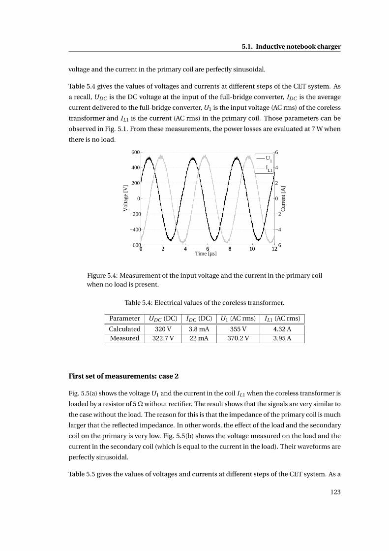
5.1. Inductive notebook charger
voltage and the current in the primary coil are perfectly sinusoidal.
Table 5.4 gives the values of voltages and currents at different steps of the CET system. As
a recall, UDC is the DC voltage at the input of the full-bridge converter, IDC is the average
current delivered to the full-bridge converter, U1 is the input voltage (AC rms) of the coreless
transformer and IL1 is the current (AC rms) in the primary coil. Those parameters can be
observed in Fig. 5.1. From these measurements, the power losses are evaluated at 7 W when
there is no load.
0 2 4 6 8 10 12−600
−400
−200
0
200
400
600
Vol
tage
[V]
0 2 4 6 8 10 12−6
−4
−2
0
2
4
6
Cur
rent
[A]
Time [µs]
U1
IL1
Figure 5.4: Measurement of the input voltage and the current in the primary coilwhen no load is present.
Table 5.4: Electrical values of the coreless transformer.
Parameter UDC (DC) IDC (DC) U1 (AC rms) IL1 (AC rms)
Calculated 320 V 3.8 mA 355 V 4.32 AMeasured 322.7 V 22 mA 370.2 V 3.95 A
First set of measurements: case 2
Fig. 5.5(a) shows the voltage U1 and the current in the coil IL1 when the coreless transformer is
loaded by a resistor of 5Ωwithout rectifier. The result shows that the signals are very similar to
the case without the load. The reason for this is that the impedance of the primary coil is much
larger that the reflected impedance. In other words, the effect of the load and the secondary
coil on the primary is very low. Fig. 5.5(b) shows the voltage measured on the load and the
current in the secondary coil (which is equal to the current in the load). Their waveforms are
perfectly sinusoidal.
Table 5.5 gives the values of voltages and currents at different steps of the CET system. As a
123

Chapter 5. Experimental results and prototypes
recall, UL is the voltage (AC rms) obtained on the load and IL is the current (AC rms) obtained in
the load. The total losses generated in the coils and the full-bridge converter can be estimated
from the measurements at 10.2 W, resulting in an efficiency of 88.9 %.
0 2 4 6 8 10 12−600
−400
−200
0
200
400
600
Vol
tage
[V]
0 2 4 6 8 10 12−6
−4
−2
0
2
4
6
Cur
rent
[A]
Time [µs]
U1
IL1
0 2 4 6 8 10 12−40
−20
0
20
40
Vol
tage
[V]
0 2 4 6 8 10 12−6
−4
−2
0
2
4
6
Cur
rent
[A]
Time [µs]
UL
IL
(a) (b)
Figure 5.5: (a) Measurement of the input voltage and the current in the primarycoil when the coreless transformer is loaded by a resistor of 5 Ω without therectifier. (b) Measurement of the voltage and the current in the load.
Table 5.5: Electrical values of the coreless transformer.
UDC (DC) IDC (DC) U1 (AC rms) IL1 (AC rms) UL (AC rms) IL (AC rms)
Calc. 320 V 234 mA 355 V 4.21 A 20.18 V 4.05 AMeas. 321.2 V 281.5 mA 358.1 V 3.80 A 21.16 V 3.79 A
First set of measurements: case 3
Fig. 5.6(a) shows the voltage U1 and the current in the coil IL1 when the coreless transformer
is loaded by a resistor of 5Ω through the rectifier. For the same reason formulated above, they
are very similar to the previous cases. Fig. 5.6(b) shows the voltage UL,eq obtained at the input
of the secondary rectifier and the current IL2 in the secondary coil. The waveforms are not
sinusoidal because of the non-linearities introduced by the diodes.
Table 5.6 gives the values of voltages and currents at different steps of the CET system. Here,
UL,DC and IL,DC are respectively the voltage and the current (DC) obtained in the load. The
total losses generated in the coils, the full-bridge converter and the full-bridge rectifier can be
estimated from the measurements at 22.6 W, resulting in an efficiency of 79.4 %.
124

5.1. Inductive notebook charger
0 2 4 6 8 10 12−600
−400
−200
0
200
400
600V
olta
ge [V
]
0 2 4 6 8 10 12−6
−4
−2
0
2
4
6
Cur
rent
[A]
Time [µs]
U1
IL1
0 2 4 6 8 10 12−30
−20
−10
0
10
20
30
Vol
tage
[V]
0 2 4 6 8 10 12−10
−5
0
5
10
Cur
rent
[A]
Time [µs]
UL,eq
IL2
(a) (b)
Figure 5.6: (a) Measurement of the input voltage and the current in the primarycoil when the coreless transformer is loaded by a resistor of 5Ωwith the rectifier.(b) Measurement of the voltage at the input of the secondary rectifier and thecurrent in the secondary coil.
Table 5.6: Electrical values of the coreless transformer.
UDC (DC) IDC (DC) U1 (AC rms) IL1 (AC rms) UL,DC (DC) IL,DC (DC)
Calc. 320 V 274 mA 355 V 4.34 A 20.06 V 4.01 AMeas. 320.4 V 345.5 mA 359.9 V 3.89 A 21.7 V 4.05 A
Second set of measurements
As explained in appendix D.2.2, the load of the notebook battery can vary during the process of
charging (as a function of the charge level, the screen brightness, CPU usage, . . . ), but in every
case, a voltage situated around 20 V (DC) is required. Therefore, it is interesting to analyze the
effect of the load variation of the system. To achieve this, an electronic load (HP 6050 DC) is
used and varied from 2 to 15Ω.
The load voltage UL,DC and the efficiency are plotted as a function of the load resistance in
Fig. 5.7. The smaller is the load (that is the larger is its corresponding resistance), the higher is
the DC voltage obtained on the load. This happens because the reflected impedance decreases
when the load resistance is increased. This leads to a slight increase of current in the primary
coil, which in turn increases the induced voltage in the secondary coil.
The measurements of efficiency take into account the losses in the transistors, in the coils
and in the diodes of the secondary rectifier. The efficiency is maximal for a load resistance
situated between 4 and 5Ω, which corresponds to the value for which the coreless transformer
is designed.
125

Chapter 5. Experimental results and prototypes
2 4 6 8 10 12 1435
40
45
50
55
60
65
70
75
80
Eff
icie
ncy
[%]
2 4 6 8 10 12 1418
19
20
21
22
23
24
25
Vol
tage
[V
]
Load [Ω]
EfficiencyLoad voltage
Figure 5.7: Efficiency and DC voltage level versus the load resistance.
5.1.5 Conclusion
Thanks to a preliminary study presented in appendix D, it is possible to draw the specifications
of the coreless transformer for the inductive notebook charger. With the analytical model
presented in chapter 2, the design of the coreless transformer is performed and a prototype is
built (c.f. Fig. 5.8(a)). The measurements show that the coreless transformer is able to provide
a minimal and stable voltage of 20 V (DC) for different values of load resistances.
The presence of the secondary rectifier generates voltage and current disturbances in the
secondary coil that deteriorate the efficiency of the whole system. The origin of this problem is
assumed to come from the addition of capacitive and inductive elements (in the rectifier and
the smoothing capacitor) that may be not consistent with the hypothesis that the equivalent
load (D.4) is purely resistive. This issue must be further investigated so as to minimize the
inherent efficiency drop.
Finally, the prototype has been tested directly on the battery while the notebook was working
(c.f. Fig. 5.8(b)). We have been able to recharge completely the battery. For us, this first
prototype allows to validate the modeling of coreless transformers.
126

5.2. CET table
(a)
(b)
Figure 5.8: (a) Picture of the prototype without the notebook. (b) Picture of theprototype while charging the notebook battery.
5.2 CET table
5.2.1 Introduction
Many aspects concerning the specifications and the design of the CET table and are discussed
in section 4.6. The present section presents three different prototypes built during this thesis,
127

Chapter 5. Experimental results and prototypes
so as to validate the different models and the optimization method presented in the previous
chapters.
First, preliminary measurements are made on two different arrays of coils. This allows to
validate the accuracy of the analytical model when multiple coils are used, and in the same
time, to identify some issues concerning the CET when using coils arrays. This first part is
presented in section 5.2.2.
Secondly, a larger prototype is built in which a new method for the detection and local
activation is implemented. This is probably the most important prototype developed in this
thesis as it includes innovative developments concerning the detection and the supply of
peripherals. The focus will be made on the electronics and the supply strategy of the CET table.
This second part is presented in sections 5.2.3 to 5.2.7.
Finally, for the third prototype, the solution proposed in Tables 4.5 and 4.6 is implemented
and measured so as to validate the optimization of the CET table. This third part is presented
in section 5.2.8.
5.2.2 First measurements
First tests and measurements are done on two different primary coils arrays. The design of the
coil 5 presented in Table 2.3 is replicated into multiple coils placed side by side. The first one
is an array of nine primary coils distributed in one layer as shown in Fig. 5.9(a). The second
one consists of an array of eighteen primary coils distributed in two shifted layers as shown in
Fig. 5.9(b). A picture of the setup that is used for the measurements is given in Fig. 5.10 with
the two-layers array and the full-bridge converter presented in section 5.1.3.
0
X
Y
0
X
Y
(a) (b)
Figure 5.9: (a) The array of 9 coils. (b) The array of 18 coils.
128

5.2. CET table
FFuullll--bbrriiddggee ccoonnvveerrtteerr
22--llaayyeerrss pprriimmaarryy ccooiill aarrrraayy MMoovviinngg llooaadd
Figure 5.10: Picture of the setup with the array of 18 coils.
For the measurements, the coil 6 of Table 2.3 is displaced over the arrays. Fig. 5.11 shows the
measured and calculated values of the voltage (AC rms) obtained on a load of 5Ω as a function
of the displacements xd and yd of the secondary coil. A grid of points separated by 5 mm is
used. The vertical distance between the primary coils and the secondary one is 5 mm. The
measurements are not performed above the whole arrays because the geometrical periodicity
of the structures would make them repetitive. A current of 1 A (AC rms) is generated in the
primary coils with the full-bridge converter working at a frequency of 220 kHz. The secondary
coil is series-compensated with a capacitor of 47 nF.
Figs. 5.11(a) and 5.11(b) show respectively the calculated and the measured load voltage
over the single-layer array. They are in good agreement. But the measurements show that a
minimal voltage of 0.3 V (AC rms) is obtained when the secondary coil is placed exactly above
the corners of four primary coils. Of course this value is not sufficient to supply electronic
peripherals.
A possible solution to solve this problem consists in using two shifted layers. Figs. 5.11(c) and
5.11(d) show respectively the calculated and the measured load voltage above the two-layers
array. The minimal voltage obtained under these conditions is about 3.3 V (AC rms).
In conclusion, this first study allows to validate the models presented in chapters 2 and 3
for primary coils arrays using PCB coils. Furthermore, it highlights the issues of CET with
primary coils arrays, in which the voltage transferred to the load is not constant in function
of the position, and may even be not sufficient to supply peripherals. A possible solution for
this problem consists in using two layers of primary coils. But this method brings two main
disadvantages. First, if it is true that a minimal amount of transferred power can be ensured at
every position, it remains inconstant over the surface, for example between 3.3 and 5.5 V (AC
rms) in Fig. 5.11(d). Secondly, concerning the problem of detection and local activation, two
129
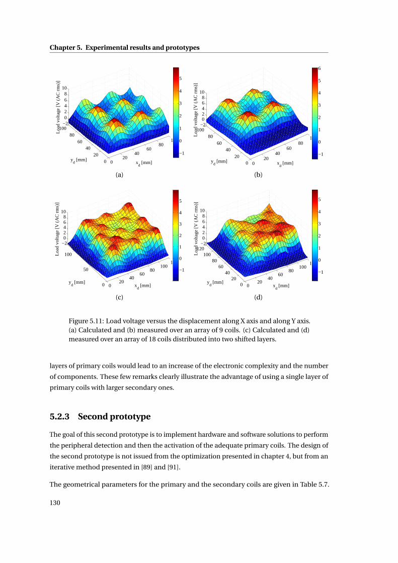
Chapter 5. Experimental results and prototypes
020
4060
80100
020
4060
80100
−202468
10
xd [mm]
yd [mm]
Load
vol
tage
[V (
AC
rm
s)]
−1
0
1
2
3
4
5
020
4060
80100
020
4060
80100
−202468
10
xd [mm]y
d [mm]
Load
vol
tage
[V (
AC
rm
s)]
−1
0
1
2
3
4
5
6
(a) (b)
020
4060
80100
120
0
50
100
−202468
10
xd [mm]
yd [mm]
Load
vol
tage
[V (
AC
rm
s)]
−1
0
1
2
3
4
5
020
4060
80100
120
020
4060
80100
120−202468
10
xd [mm]
yd [mm]
Load
vol
tage
[V (
AC
rm
s)]
−1
0
1
2
3
4
5
(c) (d)
Figure 5.11: Load voltage versus the displacement along X axis and along Y axis.(a) Calculated and (b) measured over an array of 9 coils. (c) Calculated and (d)measured over an array of 18 coils distributed into two shifted layers.
layers of primary coils would lead to an increase of the electronic complexity and the number
of components. These few remarks clearly illustrate the advantage of using a single layer of
primary coils with larger secondary ones.
5.2.3 Second prototype
The goal of this second prototype is to implement hardware and software solutions to perform
the peripheral detection and then the activation of the adequate primary coils. The design of
the second prototype is not issued from the optimization presented in chapter 4, but from an
iterative method presented in [89] and [91].
The geometrical parameters for the primary and the secondary coils are given in Table 5.7.
130

5.2. CET table
The operating frequency of the CET table is 200 kHz. At this frequency, the measured electrical
parameters for the primary coil are a resistance of 0.25 Ω and a self-inductance of 6,90 µH.
The measured electrical parameters for the secondary coil are a resistance of 0.95 Ω and a
self-inductance of 25,55 µH.
Two pictures of the prototype are given in Fig. 5.12 showing respectively a top and a bottom
view of the primary coils and electronics.
Table 5.7: Geometrical parameters of the coils for the second prototype.
Parameter Value Parameter Value
a1 40 mm a2 60 mmn1 18 n2 20N1 2 N2 2w1 1.5 mm w2 1.5 mmd1 0.5 mm d2 0.2 mm
5.2.4 Supply strategy
The system has to be able to supply only the primary coils that are situated below the peripher-
als. Therefore, the CET table detects the presence and localize the position of a peripheral. The
detection methods are presented in the next section. Once the position of the peripherals is
detected, the CET table activates only the corresponding coils. The whole process of detection
and local activation is completely autonomous and sensorless.
A DSP microcontroller (TI 28027 Piccolo) is used as the central control unit. It controls the tran-
sistors for the individual activation of primary coils, it processes the on-board measurements
for the detection of peripherals, and it manages all the supply strategy of the CET table.
Basically, this strategy can be split into four main phases that are synthesized in Fig. 5.13. The
first phase allows to calibrate the system, and the three following phases constitute an infinite
loop that controls the load detection and the coil activation. The detection is performed by
analyzing the electrical signals generated by the voltage supply. This issue is discussed in the
following section. The four phases can be defined as follows:
1. The initialization phase realizes a first scanning of each primary coil with no peripheral
on the table. The electrical signals of every single coil are measured and stored. This
first set of measurements will then serve as the reference values.
2. The detection phase starts a new scanning of all coils. The primary signals are mea-
sured and compared to the reference values. A short (about 0.5 ms) analyzis allows to
determine the presence or the absence of a load above each primary coil.
131

Chapter 5. Experimental results and prototypes
(a)
(b)
Figure 5.12: (a) Top view and (b) bottom view of the prototype.
132

5.2. CET table
3. The supply phase activates the primary coils where a load has been detected. This phase
takes most of time (about 0.5 s).
4. The clear phase deactivates all primary coils and leads to a new detection phase. This
phase is very short (much less than 1 ms).
First scanning On-boardmeasurements
Storage ofreference values
Initialization phase
ScanningOn-boardmeasurements
Comparison withreference values
Determination ofload presence
Detection phase
Activation ofswitches
Supply ofprimary coils
Supply phase
Deactivationof switches
Stopping supplyof primary coils
Clear phase
Figure 5.13: General strategy used for the CET table.
In brief, the operating strategy consists of an alternating sequence of detection phases and
supply phases. Consequently, three different scales of time or frequency are used in the CET
table, as explained in Fig. 5.14.
First, the supplying process is interrupted by the detection phases at intervals of about 0.5 s.
This duration may be decreased depending on the desired reactivity of the peripherals detec-
tion. However, experimental tests have shown that the detection phase should be no longer
than a few milliseconds in order not to perturb or interrupt the energy transfer. Keeping this
value under 5 ms ensures no discontinuity of the peripherals supplying.
Secondly, the scanning of the primary coils consists in activating individually each coil during
a very short time. Typically, the activation of every single coils lasts from 10 to 100 µs, which is
in agreement with the maximal duration of a few ms for the detection phase.
Thirdly, the activated coils are excited by a high-frequency current of about 200 kHz. This case
occurs during the supply phase and during the short activation of every coils for the detection.
133

Chapter 5. Experimental results and prototypes
//
//
~2 ms
~0.5 sSupply phase
Detection phase
Individual scanningwindows of the
coils
High-frequencysinewave current
(~200 kHz)
1st 2nd 3rd ... 36th~50 µs
~5 µs
Figure 5.14: Different time scales for the signals applied to the primary coils array.
5.2.5 Primary coils array circuit
Primary layout
For a large CET surface, the number of electronic components may become very important
and therefore the manufacturing cost and complexity of integration very high. In order to
reduce the number of components, a specific electronic circuit allowing to activate individual
primary coils has been developed. Its general layout is shown in Fig. 5.15. The coils are
arranged in an array, where it is possible to control the rows and the columns independently.
Each coil is represented by an inductor and a resistor in series.
The concept consists in managing all the primary coils as a function of their row and column
arrangement. This is realized by connecting all the primary coils of a row to the same line and
repeating the same process to columns. As a result, the column switches control the column
lines and the row switches control the row lines. Switching on one row and one column allows
to activate the corresponding single coil, as highlighted in Fig. 5.15.
A resonant capacitor is placed in parallel to each coil, so that if multiple primary coils are
activated simultaneously, there is no need to tune the operating frequency. Furthermore, a
diode must be added in series with every coil. This prevents the current from flowing back to
other inactive coils.
134
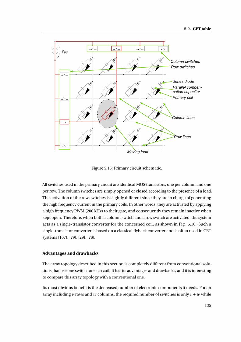
5.2. CET table
VDC
Column switchesRow switches
Series diodeParallel compen-sation capacitorPrimary coil
Row lines
Column lines
Moving load
Figure 5.15: Primary circuit schematic.
All switches used in the primary circuit are identical MOS transistors, one per column and one
per row. The column switches are simply opened or closed according to the presence of a load.
The activation of the row switches is slightly different since they are in charge of generating
the high frequency current in the primary coils. In other words, they are activated by applying
a high frequency PWM (200 kHz) to their gate, and consequently they remain inactive when
kept open. Therefore, when both a column switch and a row switch are activated, the system
acts as a single-transistor converter for the concerned coil, as shown in Fig. 5.16. Such a
single-transistor converter is based on a classical flyback converter and is often used in CET
systems [107], [79], [29], [76].
Advantages and drawbacks
The array topology described in this section is completely different from conventional solu-
tions that use one switch for each coil. It has its advantages and drawbacks, and it is interesting
to compare this array topology with a conventional one.
Its most obvious benefit is the decreased number of electronic components it needs. For an
array including v rows and w columns, the required number of switches is only v +w while
135

Chapter 5. Experimental results and prototypes
x
~~~ ~~~~~ ~~
~ 200 kHz
VDC
moving load
Column switches
Row switches
Figure 5.16: Single-transistor converter.
typical solutions use v ·w switches. For instance, the prototype presented in this section uses
only 6+6 = 12 MOS transistors instead of 36 that would be necessary for each primary coil.
Furthermore, the control of the activation is quite simple since only the 6 rows and the 6
columns have to be switched. Thanks to this small number of switches to be controlled, it is
possible to connect them directly to the microcontroller without any demultiplexer.
The second advantage of this primary topology is that it allows to integrate a single detection
system that is common to all the primary coils instead of using individual detection systems
for each primary coil. This reduces drastically the number of components and wires required
by the primary array.
However, this topology has also its drawbacks. The main one consists of an unwanted activa-
tion of some specific coils when multiple peripherals are placed on the table. Indeed, like for
the activation of a single primary coil, when two coils belonging to the same row or column
are activated, there is no problem. This case is shown in Fig. 5.17(a). But when two coils that
belong to neither the same row nor the same column have to be activated, this automatically
turns on two more coils situated at their opposite cross-sections. This case is shown in Fig.
5.17(b). It is not dramatic if the number of loads is not too high, but for a table that has a large
surface, it could limit the number of peripherals that can be so supplied. A solution to this
problem could be to fragment the table into multiple subparts that work independently of
each other. But for the prototype that is presented in this section, this is not an issue.
136
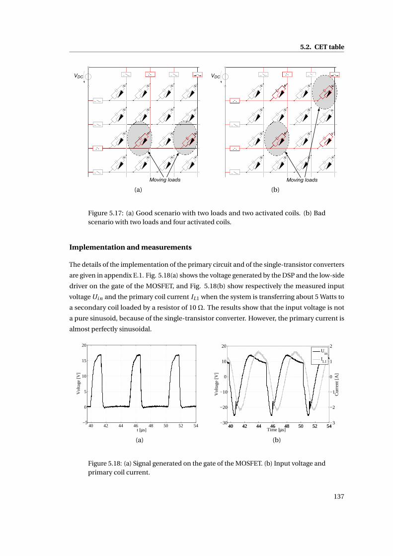
5.2. CET table
VDC
Moving loads
VDC
Moving loads
(a) (b)
Figure 5.17: (a) Good scenario with two loads and two activated coils. (b) Badscenario with two loads and four activated coils.
Implementation and measurements
The details of the implementation of the primary circuit and of the single-transistor converters
are given in appendix E.1. Fig. 5.18(a) shows the voltage generated by the DSP and the low-side
driver on the gate of the MOSFET, and Fig. 5.18(b) show respectively the measured input
voltage Ui n and the primary coil current IL1 when the system is transferring about 5 Watts to
a secondary coil loaded by a resistor of 10 Ω. The results show that the input voltage is not
a pure sinusoid, because of the single-transistor converter. However, the primary current is
almost perfectly sinusoidal.
40 42 44 46 48 50 52 54−5
0
5
10
15
20
t [µs]
Vol
tage
[V]
40 42 44 46 48 50 52 54−30
−20
−10
0
10
20
Vol
tage
[V]
40 42 44 46 48 50 52 54−3
−2
−1
0
1
2
Cur
rent
[A]
Time [µs]
Uin
IL1
(a) (b)
Figure 5.18: (a) Signal generated on the gate of the MOSFET. (b) Input voltage andprimary coil current.
137
Chapter 5. Experimental results and prototypes
5.2.6 Peripheral detection
Detection methods
Depending on the presence of a load above a primary coil, the equivalent impedance seen by
the voltage source is changed. As a result, the current and the voltage on the primary coil are
as well changed. With the microcontroller and an adequate shaping electronic circuit, it is
possible to detect these differences and determine the presence or absence of a peripheral.
Basically, two main effects can be observed depending on the presence of a load and on the
load itself.
The first one is the variation of the phase shift between the primary current and the input
voltage. Theoretically, the resistance of the primary coil is insignificant compared to its
inductive impedance. Then, if there is no load above it, the phase shift between the current
and voltage of the primary coil is nearly φ = 90 and no active power is consumed except for
Joule losses in the primary coil. For instance, the phase angle of the primary coil defined in
Table 5.7 is given by:
φ= arg(U i n)−arg(I L1) = arg(R1 + jωL1) = 88.34 (5.1)
If there is a secondary coil with a load above it, then the phase shift decreases (φ< 90), and the
greater is the load the smaller is the phase shift. This means that active power is consumed in
the CET process. For instance, if there is a secondary coil perfectly aligned with a primary coil
and if the secondary coil is loaded by a resistor of 10Ω, the phase shift between the primary
current and the voltage is given by:
φ= arg(U i n)−arg(I L1) = 54.81 (5.2)
So it is possible to use this effect to perform the peripherals detection. However, the phase shift
detection circuit is complicated to implement because it requires two distinct measurement
circuits for the current phase and the voltage phase [112].
The second effect that can be exploited is the amplitude of the primary coil current and the
amplitude of the input voltage. Due to the PS compensation topology, the voltage amplitude
is difficult to measure because its variation as a function of the load presence is not significant.
The current amplitude is more convenient to measure, because it is a relatively pure sinusoid
and because its amplitude variation is much more significant. The cause for this that the
presence of a load creates a reflected impedance on the primary circuit which leads to a
decrease of the primary current amplitude.
Implementing all the electronic circuits for the phase shift, the voltage amplitude and the
138
5.2. CET table
current amplitude could allow to evaluate accurately the total impedance of the system, and
the impedance of the load itself could then be deduced. Such a system is proposed in [112].
However, it requires four distinct electronic circuits, which is not in adequation with the
guideline of restricting the number of components.
Hence, it has been decided to implement only the current amplitude evaluation circuit pre-
sented in Fig. 5.19. The originality here is that this circuit is placed in series with the DC
voltage supply so that its delivered current is measured. Doing so allows to use a single circuit
for every primary coil. The strategy to determine the presence or the absence of a consumer
simply consists in fixing a threshold value on the difference between the current amplitude
measured during the calibration phase and the one measured during each detection phase. If
this threshold value is exceeded, the presence of a load is declared positive for the concerned
primary coil. All this process is continuously controlled by the DSP.
The main electronic components of the detection circuit are presented in details in appendix
E.2. The current is evaluated by amplifying the voltage obtained on a shunt resistor RS . A low-
pass filter with a cut-off frequency of about 500 kHz is implemented to reduce the noise, and
the resulting signal is then routed through a limiting current resistor to the analog-to-digital
(A/D) converter of the microcontroller. As a result, the current amplitude of each coil can be
evaluated, stored and compared to the calibrated values.
+
-
VDCRS
R1
R2
IIN
R3
C1
GND
R4
GND
3.3 V
mC-ADU7
D1
D2+15 V
-15 V
Figure 5.19: Circuit implemented for the estimation of the current.
Measurements
As a first set of measurements, the current generated by the voltage supply is measured in
four different cases. First when there is no load on the tested coil, and then in the three cases
presented in Fig. 4.18, that correspond respectively to when the secondary coil is perfectly
aligned with a primary coil (case 1), when the secondary coil is placed between two primary
coils (case 2), and when the primary coil is place between four primary coils (case 3). The
secondary coil is loaded by a resistor of 10Ω.
139

Chapter 5. Experimental results and prototypes
Fig. 5.20(a) shows the measurements of the current generated by the voltage supply, and
Fig. 5.20(b) shows the measurements of the voltage provided to the A/D converter of the
DSP (which corresponds to the output of the circuit presented in Fig. 5.19). Some noise is
generated at the output of the detection circuit due to the switching transistors. However, it
does not cause any problems because the A/D conversion is programmed to occur at the time
where the voltage is at its maximum, thus avoiding the switching instant.
0 5 10 15−1
−0.5
0
0.5
1
1.5
t [µs]
Cur
rent
[A]
Case 1
Case 2Case 3
No load
0 5 10 150
0.5
1
1.5
2
2.5
3
t [µs]
Vol
tage
[V
]
No loadCase 3
Case 1
Case 2
(a) (b)
Figure 5.20: (a) Current generated by the voltage supply. (b) Voltage provided tothe A/D converter of the DSP.
For the second set of measurements, the three different time scales depicted in Fig. 5.14 are
presented. Fig. 5.21 shows the current delivered by the voltage supply for different cases.
In Figs. 5.21(a)-(b)-(c), the current is measured over a duration of 2 seconds when respectively
no primary coil, one primary coil and two primary coils have detected the presence of a
load and therefore are activated. For this time scale, the supply and detection phases can be
observed. The supply phase shows different amplitudes of current as a function of the number
of activated primary coils, and the detection phase takes the form of short peaks. As it can be
observed, four detection phases per seconds are achieved so as to have a good reactivity for
the peripheral detection.
In Figs. 5.21(d)-(e)-(f), a zoom is made on a single detection phase when respectively no
primary coil, one primary coil and two primary coils have detected the presence of a load.
A whole detection phase lasts for about 2 ms during which each primary coil is separately
activated. In this specific case, 36 intervals can be observed (one per primary coil), and it is
interesting to note that the current amplitude is higher for the coils that detect the presence of
a load. For example, in Fig. 5.21(e), a secondary loaded coil is placed above the 24-th scanned
coil and in Fig. 5.21(f), two secondary coils are placed above respectively the 12-th and 24-th
coils.
140
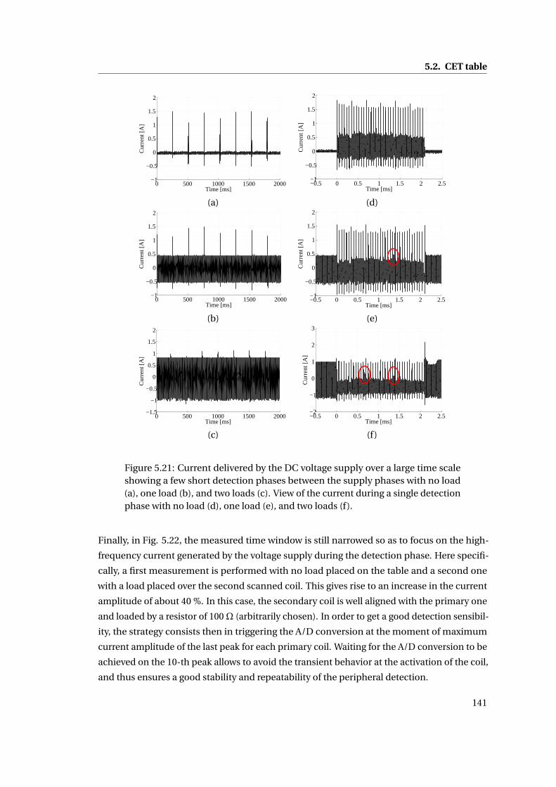
5.2. CET table
0 500 1000 1500 2000−1
−0.5
0
0.5
1
1.5
2
Cur
rent
[A]
Time [ms]−0.5 0 0.5 1 1.5 2 2.5−1
−0.5
0
0.5
1
1.5
2
Cur
rent
[A]
Time [ms]
(a) (d)
0 500 1000 1500 2000−1
−0.5
0
0.5
1
1.5
2
Cur
rent
[A]
Time [ms]−0.5 0 0.5 1 1.5 2 2.5−1
−0.5
0
0.5
1
1.5
2
Cur
rent
[A]
Time [ms]
(b) (e)
0 500 1000 1500 2000−1.5
−1
−0.5
0
0.5
1
1.5
2
Cur
rent
[A]
Time [ms]−0.5 0 0.5 1 1.5 2 2.5−2
−1
0
1
2
3
Cur
rent
[A]
Time [ms]
(c) (f)
Figure 5.21: Current delivered by the DC voltage supply over a large time scaleshowing a few short detection phases between the supply phases with no load(a), one load (b), and two loads (c). View of the current during a single detectionphase with no load (d), one load (e), and two loads (f).
Finally, in Fig. 5.22, the measured time window is still narrowed so as to focus on the high-
frequency current generated by the voltage supply during the detection phase. Here specifi-
cally, a first measurement is performed with no load placed on the table and a second one
with a load placed over the second scanned coil. This gives rise to an increase in the current
amplitude of about 40 %. In this case, the secondary coil is well aligned with the primary one
and loaded by a resistor of 100Ω (arbitrarily chosen). In order to get a good detection sensibil-
ity, the strategy consists then in triggering the A/D conversion at the moment of maximum
current amplitude of the last peak for each primary coil. Waiting for the A/D conversion to be
achieved on the 10-th peak allows to avoid the transient behavior at the activation of the coil,
and thus ensures a good stability and repeatability of the peripheral detection.
141

Chapter 5. Experimental results and prototypes
0.04 0.05 0.06 0.07 0.08 0.09 0.1 0.11 0.12 0.13 0.14−1
−0.5
0
0.5
1
1.5
2
Cur
rent
[A]
Time [ms]
No loadWith load
First coil Third coilSecond coil
A/D conversion
Figure 5.22: Zoom on the second coil scanning with and without load.
5.2.7 Secondary coils circuit
The schematic of the secondary circuit is shown in Fig. 5.23 and its main components are
described in details in appendix E.3. A full-bridge rectifier with a smoothing capacitor allows
to convert the 200 kHz induced voltage to a DC voltage. The level of the DC voltage is then
adapted to the needs of the peripheral. For example, for the loudspeaker, a voltage regulator
(called U1 in Fig. 5.23) allows to obtain the required voltage of 5 V (DC). Similar circuits are
used for the mouse and the keyboard.
R2
L22
C2
D2
D1
D3
D4
CU1 CU2
U1
RL UL,DCUL,eq
Figure 5.23: Secondary circuit scheme for the speaker providing a 5 V (DC) output.
Fig. 5.24 shows typical measurements of currents and voltages obtained on the secondary
circuit. Here, they are made when the secondary coil is well aligned with a primary coil, but
similar results are obtained for other scenarios. Two different cases are showed.
First, Fig. 5.24(a) gives the voltage UL and the current IL obtained on a load of 10Ωwhen there
142

5.2. CET table
is no rectifier and no voltage regulator.
Secondly, Fig. 5.24(b) gives the DC voltage UL,DC and current IL,DC obtained on a load of 10Ω
when there is a rectifier but no voltage regulator. The voltage UL,eq measured at the input of
the rectifier and the secondary coil current IL2 are also shown.
The results show that the current generated in the secondary coil is nearly identical with and
without rectifier. This confirms that the presence of the rectifier has no significant impact
on the value of the load. The voltage UL measured without rectifier is nearly sinusoidal, but
when a rectifier is used, the voltage UL,eq has a square-wave shape. One can as well notice
that the load voltage UL,DC shown in Fig. 5.24(b) is slightly lower than the amplitude of the
square-wave voltage UL,eq . This is due to the forward voltage drop in the diodes of the rectifier.
0 5 10 15−15
−10
−5
0
5
10
15
Vol
tage
[V]
0 5 10 15−1.5
−1
−0.5
0
0.5
1
1.5
Cur
rent
[A]
Time [µs]
UL
IL
0 5 10 15−10
−5
0
5
10
Vol
tage
[V]
0 5 10 15−1.5
−1
−0.5
0
0.5
1
1.5
Cur
rent
[A]
Time [µs]
UL,eq
IL2
UL,DC
IL,DC
(a) (b)
Figure 5.24: (a) Voltage and current measured on a load of 10Ωwithout rectifier.(b) Voltage and current measured at the input and at the output of the rectifierloaded by a resistor of 10Ω.
Finally, Table 5.8 gives multiple measurements of power and efficiency using different loads
in different scenarios. A rectifier is used for each measurement. The three different cases
described in Fig. 4.18 are measured for a load of 5Ω, a load of 10Ω, a load of 100Ω and the
loudspeaker.
The voltage supply is set to 18 V (DC) as this value allows to create an input voltage Ui n of
12 V (AC rms) on the primary coils. The power delivered by the source is then calculated by
multiplying its DC voltage (18 V (DC)) by its average current. The voltage UL,DC obtained in
the load is measured with a multimeter and the corresponding power PL is easily derived. As a
result, the efficiency η takes into account the losses in the transistors, in the coils and in the
rectifier.
For the loudspeaker, the losses in the voltage regulator are also taken into account, and UL,DC
143
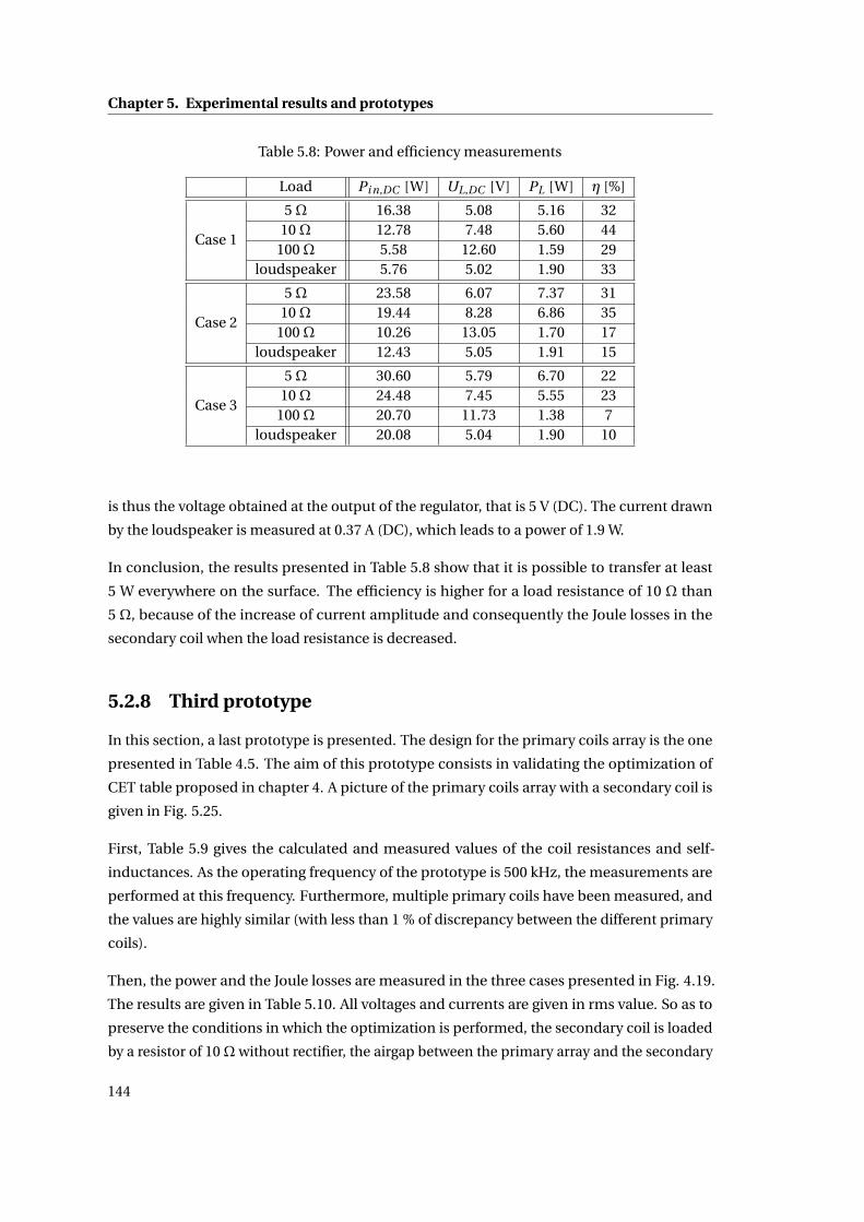
Chapter 5. Experimental results and prototypes
Table 5.8: Power and efficiency measurements
Load Pi n,DC [W] UL,DC [V] PL [W] η [%]
Case 1
5Ω 16.38 5.08 5.16 3210Ω 12.78 7.48 5.60 44
100Ω 5.58 12.60 1.59 29loudspeaker 5.76 5.02 1.90 33
Case 2
5Ω 23.58 6.07 7.37 3110Ω 19.44 8.28 6.86 35
100Ω 10.26 13.05 1.70 17loudspeaker 12.43 5.05 1.91 15
Case 3
5Ω 30.60 5.79 6.70 2210Ω 24.48 7.45 5.55 23
100Ω 20.70 11.73 1.38 7loudspeaker 20.08 5.04 1.90 10
is thus the voltage obtained at the output of the regulator, that is 5 V (DC). The current drawn
by the loudspeaker is measured at 0.37 A (DC), which leads to a power of 1.9 W.
In conclusion, the results presented in Table 5.8 show that it is possible to transfer at least
5 W everywhere on the surface. The efficiency is higher for a load resistance of 10 Ω than
5 Ω, because of the increase of current amplitude and consequently the Joule losses in the
secondary coil when the load resistance is decreased.
5.2.8 Third prototype
In this section, a last prototype is presented. The design for the primary coils array is the one
presented in Table 4.5. The aim of this prototype consists in validating the optimization of
CET table proposed in chapter 4. A picture of the primary coils array with a secondary coil is
given in Fig. 5.25.
First, Table 5.9 gives the calculated and measured values of the coil resistances and self-
inductances. As the operating frequency of the prototype is 500 kHz, the measurements are
performed at this frequency. Furthermore, multiple primary coils have been measured, and
the values are highly similar (with less than 1 % of discrepancy between the different primary
coils).
Then, the power and the Joule losses are measured in the three cases presented in Fig. 4.19.
The results are given in Table 5.10. All voltages and currents are given in rms value. So as to
preserve the conditions in which the optimization is performed, the secondary coil is loaded
by a resistor of 10Ωwithout rectifier, the airgap between the primary array and the secondary
144

5.2. CET table
Figure 5.25: Picture of the primary coils array and the secondary coil.
Table 5.9: Parameters of the primary and secondary coils
L1 [µH] R1 [Ω] L2 [µH] R2 [Ω]Measured 14.25 1.29 13.45 0.93Calculated 13.42 1.03 13.12 0.82
coil is 5 mm. A voltage input of approximately 24 V (AC rms) is generated in the primary coils
using the full-bridge converter presented in section 5.1.3. The Joule losses of the primary
coils and of the secondary coil (respectively P j 1 and P j 2) are calculated using the values of
the measured resistances (respectively R1 and R2) and the values of the measured currents
(respectively IL1 and IL2). For the case b, the current in the two primary coils is measured,
and for the case c, the current in the three primary coils is measured. Finally, The efficiency
estimation takes into account only the Joule losses in the coils.
The measured results are in good agreement with the calculated ones. The main difference
concerns the losses. Indeed, the calculated values for the losses are underevaluated. This is
mainly due to the calculated resistances of the coils that are also slightly underestimated in the
model. This difference is probably caused by imperfections of the PCB copper tracks, because
even the calculated DC resistances have a lower value than the measured ones. However, this
difference is not significant and the results obtained with this third prototype validate the
optimization method presented in chapter 4.
145
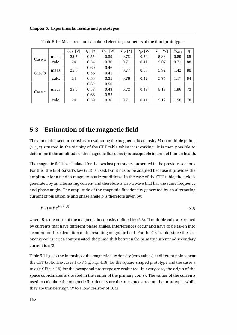
Chapter 5. Experimental results and prototypes
Table 5.10: Measured and calculated electric parameters of the third prototype.
Ui n [V] IL1 [A] P j 1 [W] IL2 [A] P j 2 [W] PL [W] Ploss η
Case ameas. 25.5 0.55 0.39 0.73 0.50 5.33 0.89 85calc. 24 0.54 0.30 0.71 0.41 5.07 0.71 88
Case bmeas. 25.6
0.60 0.460.77 0.55 5.92 1.42 80
0.56 0.41calc. 24 0.58 0.35 0.76 0.47 5.74 1.17 84
Case cmeas. 25.5
0.62 0.500.72 0.48 5.18 1.96 720.58 0.43
0.66 0.55calc. 24 0.59 0.36 0.71 0.41 5.12 1.50 78
5.3 Estimation of the magnetic field
The aim of this section consists in evaluating the magnetic flux density B on multiple points
(x, y, z) situated in the vicinity of the CET table while it is working. It is then possible to
determine if the amplitude of the magnetic flux density is acceptable in term of human health.
The magnetic field is calculated for the two last prototypes presented in the previous sections.
For this, the Biot-Savart’s law (2.3) is used, but it has to be adapted because it provides the
amplitude for a field in magneto-static conditions. In the case of the CET table, the field is
generated by an alternating current and therefore is also a wave that has the same frequency
and phase angle. The amplitude of the magnetic flux density generated by an alternating
current of pulsation w and phase angle β is therefore given by:
B(t ) = Be j (ωt+β) (5.3)
where B is the norm of the magnetic flux density defined by (2.3). If multiple coils are excited
by currents that have different phase angles, interferences occur and have to be taken into
account for the calculation of the resulting magnetic field. For the CET table, since the sec-
ondary coil is series-compensated, the phase shift between the primary current and secondary
current is π/2.
Table 5.11 gives the intensity of the magnetic flux density (rms values) at different points near
the CET table. The cases 1 to 3 (c.f. Fig. 4.18) for the square-shaped prototype and the cases a
to c (c.f. Fig. 4.19) for the hexagonal prototype are evaluated. In every case, the origin of the
space coordinates is situated in the center of the primary coil(s). The values of the currents
used to calculate the magnetic flux density are the ones measured on the prototypes while
they are transferring 5 W to a load resistor of 10Ω.
146

5.3. Estimation of the magnetic field
Table 5.11: Estimation of the magnetic flux density at different points above thetwo CET prototypes.
Prototype Case Position (x, y, z) [mm] Mag. flux density [µT]
Square coils
1
(0,0,20) 256.35(0,0,100) 6.80(50,0,20) 32.86
(50,0,100) 4.56(100,0,20) 3.44
(100,0,100) 1.91
2
(0,0,20) 263.37(0,0,100) 8.29(50,0,20) 48.94
(50,0,100) 5.65(100,0,20) 4.57
(100,0,100) 2.41
3
(0,0,20) 262.78(0,0,100) 10.83(50,0,20) 58.00
(50,0,100) 7.59(100,0,20) 6.51
(100,0,100) 3.39
Hexagonal coils
a
(0,0,20) 214.25(0,0,100) 3.05(50,0,20) 12.54
(50,0,100) 2.01(100,0,20) 1.47
(100,0,100) 0.84
b
(0,0,20) 217.13(0,0,100) 3.86(50,0,20) 15.19
(50,0,100) 2.57(100,0,20) 1.95
(100,0,100) 1.09
c
(0,0,20) 206.44(0,0,100) 4.69(50,0,20) 2.86
(50,0,100) 28.62(100,0,20) 3.24
(100,0,100) 2.83(100,0,100) 1.44
In [25], the limits for the human exposure to magnetic fields are defined. They are calculated
on the basis of a maximal energy that can be absorbed in human tissues without being harmed.
The basic restrictions for the current density generated in the body by a magnetic field are
147

Chapter 5. Experimental results and prototypes
precisely defined, but are practically difficult to measure. Besides those basic restrictions,
the general limits of the magnetic field intensities are given, which allow to ensure that the
basic restrictions are not exceeded. However, the converse is not necessarily true, that is if the
general limits are exceeded, it does not mean that the basic restrictions are violated.
According to [25], the maximal intensity of the magnetic flux density is dependent on the
frequency. For the square-shaped prototype working at 200 kHz, the general limit is fixed at
4.60 µT. For the hexagonal-shaped prototype working at 500 kHz, the general limit is fixed at
1.84 µT. The results of Table 5.11 show that these limits are often exceeded when the evaluation
is performed very close to the coils. But when the distance of evaluation becomes greater than
about 150 mm, the intensity of the magnetic flux density is acceptable.
Practically, for the CET table that aims to supply different peripherals, it means that only the
hands and a small portion of the arms are immersed in potentially too intense magnetic fields.
For us, as only a small portion of the body is concerned, the prototypes are estimated to be
valid, but more tests should be done on samples of human tissues to definitely confirm this
statement.
5.4 Conclusion
In this chapter, the different prototypes built during this thesis work are presented and tested.
They contribute largely to the validation of the different models and the optimization method
presented in the previous chapters.
The main effort has been placed in the prototype presented in sections 5.2.3 to 5.2.7. Therein,
a specific primary coils topology has been developed so as to limit as much as possible the
number of electronic components. In this sense, an efficient method to detect the peripherals
and selectively activate the primary coils is presented. The system is controlled by a single
DSP and is completely autonomous. Finally, different tests and measurements have shown
that the system is able to provide at least a power of 5 W over the whole surface.
Finally, the last section gives a general overview of the magnetic field densities that are at stake
when using a CET table and discusses the inherent health issues.
148

CHAPTER 6
Conclusion
6.1 Overview
This thesis addresses the modeling, design and optimization of inductive CET systems. In the
domain of electronic devices and especially desktop peripherals, inductive CET clearly appears
as the technology to investigate. Just like wireless communication protocols, it responds to
the omnipresent demand of electronic industry for removing cables, plugs, adaptors, chargers
or batteries that pollute domestic and professional environments.
In preamble of this thesis, a state of the art presents available products and current researches
dealing with inductive CET, highlighting the main issue concerning the design of such systems.
Indeed, the developed solutions are designed only for single applications and are often not
optimized. So there is an obvious lack of design and optimization methods applicable to
any inductive CET problem, and the aim of this thesis is to fill this gap. To achieve this,
the conception of the problem is separated into multiple subparts that can be individually
modified or adapted for different applications. Such a modular approach is the key point of
this thesis, as it allows to englobe a very large panel of CET solutions with a relatively simple
design methodology. Furthermore, it endorses the accessibility to the developments made in
the scope of this work, as they are expected to be reused by other engineers and researchers in
the future. It would be indeed easy for them to modify individual parts or add developments
of their own without compromising the rest of the design. Several issues concerning CET are

Chapter 6. Conclusion
addressed, notably an analytical model of inductances and its numerical implementation, the
FEM model allowing to calculate the resistance at high frequency, and the equivalent electric
model of the coreless transformer through different compensation topologies. Besides, an
optimizer using multiobjective genetic algorithms is developed in order to exploit effectively
the modeling and to generate the design of different CET systems. Finally, as for validation of
the modeling and optimization methods, fully functional prototypes are designed, built and
successfully tested.
6.2 Main results and innovative contributions
The main results and original contributions are summarized in the following points:
• Accurate modeling of coreless transformers: Analytical and numerical models, taking into
account coils resistance and different compensation topologies, allow to predict accu-
rately the behavior of inductive coils and coreless transformers. They are implemented
in a way that makes them highly adaptable and low-consuming in term of computation
time. Besides, an estimation of the magnetic field intensities has made it possible to
assess the related health risks.
• High frequency effects for PCB coils: A new method based on FEM simulations is pre-
sented and confronted to another numerical one issued from literature. The former
outpasses by far the latter in term of accuracy, but in return requires larger computing
resources. Therefore, a complete output mapping together with an interpolation strat-
egy using DOE exploit cleverly FEM simulations so as to address this problem without
compromising the accuracy of the results.
• Multiobjective genetic algorithms: A new MOGA based on the classical NSGA-II has been
implemented. Some major improvements are brought to the general working of the
algorithm and to different genetic operators. The new MOGA has then been submitted
to different test functions and applied to the design of CET systems. It has proven to
provide a fast convergence while maintaining an excellent diversity of solutions.
• Design method for the CET table: For free position systems, using a single-layer array of
primary coils with a larger secondary one has been identified as the most interesting
solution. A novel design method based on the evaluation of the transferred power and
the Joule losses for multiple positions of the secondary coil is presented. It allows to
generate an optimal solution in term of efficiency and, in the same time, it ensures the
uniformity of the transferred power above the CET surface.
• Implementation of the CET table and its detection system: An innovative activation
150

6.3. Outlook and perspectives
strategy of the primary coils has been developed. It consists of specific coils connexions
based on an arrangement of rows and columns so as to minimize the number of required
electronic components. Besides the primary coil activation, a single detection system
has been implemented for the whole CET table instead of multiple ones as encountered
in earlier works. It is based on the analyzis of the current amplitude delivered by the
voltage supply and in this sense is fully sensorless. Finally, digital control techniques
have enabled the autonomous management of the peripherals detection and coils
activation.
The collaboration with the industrial partner has enabled to have a clear view on the objectives
that consisted in modeling and implementing different CET prototypes. So as to reach that
goal, many scientific problems have been addressed. The inherent researches resulted to
five publications presented in international conferences (ICEM2010, ECCE2010, ICEMS2011,
EPE2011, ICEMS2012) and one article published in a transaction journal (Industry Applications
2011).
6.3 Outlook and perspectives
Having adopted a modular conception of CET systems encourages the promotion of further
researches in this domain and consequently their integration to the ones achieved during
this thesis work. The future developments that are more likely to share a link with this thesis,
among the multitude of existing ones, are summarized in the following points:
• Modeling of the losses in the transistors: The models and optimization presented in this
thesis are focused on the coreless transformer. It makes sense because this is the most
sensitive part in CET systems. The losses in the transistor are very complex to modelize,
and have been only studied superficially because it was not an issue for the success
of the thesis objectives. However, it would be very interesting to develop a complete
model of the losses in the transistors, as they have surely a significant impact on the
overall efficiency of CET systems, especially when the operating frequency is increased.
In the same vein, investigating the methods called zero voltage switching (ZVS) or soft
switching could be of greatest interest.
• Thermal modeling: The increase of temperature in the coils when the CET system
is loaded may become a limiting factor to the amount of transferred power. For the
different prototypes presented in this thesis, this was not an issue as Joule losses were in
the order of 0.5 W per coils, leading to temperatures that remained below 50 C. However,
a thermal modeling could be integrated to the ones of coreless transformer, so as to
provide a multi-physic approach for the optimization of CET systems.
151

Chapter 6. Conclusion
• Shielding: The advantage of adding a shielding under the primary coils and above the
secondary coils would be twofold. First it would increase the inductances of the coils
and thus their quality factor. Secondly it would reduce the intensity of the radiated
magnetic field in the surrounding of CET systems. The presence of ferro-magnetic
and/or conductive material would have a significant impact on CET systems, which
should be studied in detail.
• Primary current control: The different prototypes presented in this thesis are directly
supplied by voltage supplies. It could be however interesting to implement a system that
allows to control the current generated into the primary coil, by dynamically adapting
the input voltage level for example. Doing so could lead to a real-time regulation of the
transferred power.
• Prototype: Only a small version of the optimized design has been prototyped in order
to verify and validate the optimization method. It could be interesting to realize a
larger one that also integrates the digital control for the peripheral detection and local
activation.
• Load recognition: A system allowing to recognize the load should be implemented.
By analyzing thoroughly the current and the voltage of the primary coil, it should be
possible to avoid the activation of CET if an undesired material is placed on the table.
Still further, it should be possible to recognize exactly the load present on the table so as
to adapt the power to transfer. The electronic implementation and the digital control of
such a load recognition would be a great challenge.
Despite these possible improvements, this thesis has successfully proven the feasibility of a
CET table for multiple peripherals. The different developments and researches can be easily
reused by other engineers and leave a door open to the design of future CET applications.
In conclusion, a last reflexion is proposed concerning the ongoing standardization of CET
systems. At the beginning of this thesis work, the WPC (Wireless Power Consortium) was in its
very early days. But for a few years, it has been gaining more and more success and reputation
from both industrial and academic worlds. Our intuition is that aiming to set the standards
for inductive CET is the right strategy to further promote this technology. Not so far in the
future, the WPC may become unavoidable for designing industrial CET products. We therefore
strongly recommend to future CET engineers to keep a close watch on the WPC and, more
generally, to the development of standards.
152

APPENDIX A
Electric Modeling Equations
A.1 Series Compensated Secondary: Voltage Source Be-
havior
A series compensated secondary in coreless transformers leads to a voltage source behavior.
This can be easily verified using equations (2.28), and (2.30) to (2.34) for a given coreless
transformer, as for instance the one composed of coils 5 and 6 (so defined in section 2.2.5).
Fig. A.1(a) shows the load current versus the load voltage when the primary coil current is
maintained at a constant value of 1 A (rms), and when the load resistance is varied from 10 to
100Ω (arbitrarily chosen). This clearly shows that a secondary capacitor in series results in a
stable voltage supply. The power in the load is then given by:
PL = U 2L
RL(A.1)
where UL is the voltage on the load and RL the load resistance.
In Fig. A.1(b), the power transferred to the load versus the resistance of the load is plotted. The
curve is a typical one of a voltage supply.

Appendix A. Electric Modeling Equations
7.6 7.8 8 8.2 8.40
0.2
0.4
0.6
0.8
Load voltage (RMS) [V]
Loa
d cu
rren
t (R
MS)
[A
]
0 20 40 60 80 1000
1
2
3
4
5
6
7
Load resistance [Ω]
Loa
d po
wer
[W
]
(a) (b)
Figure A.1: Behavior of the coreless transformer (coils 5 and 6) when the loadresistance varies from 10 to 100Ω.
A.2 Parallel Compensated Secondary: Current Source
Behavior
A parallel compensated secondary in coreless transformers leads to a current source behavior.
This can be easily verified using equations (2.28), and (2.35) to (2.37). Using the coreless
transformer composed of coils 5 and 6 and maintaining the primary coil current at 1 A (rms),
the characteristic of the load voltage versus the load current is illustrated in Fig. A.2(a). This
clearly shows that a secondary capacitor in parallel results in a stable current source. The
power in the load can thus be defined as follows:
PL = RL I 2L (A.2)
where IL is the current in the load.
In Fig. A.2(b), the power transferred to the load versus the resistance of the load is plotted. The
curve is a typical one of a current source.
154

A.2. Parallel Compensated Secondary: Current Source Behavior
0 10 20 30 40 500.35
0.4
0.45
0.5
Load voltage (RMS) [V]
Loa
d cu
rren
t (R
MS)
[A
]
0 20 40 60 80 1000
5
10
15
Load resistance [Ω]
Loa
d po
wer
[W
]
(a) (b)
Figure A.2: Behavior of the coreless transformer (coils 5 and 6) when the loadresistance varies from 10 to 100Ω.
155

Appendix A. Electric Modeling Equations
A.3 Behavior of the four topologies
In the two previous sections, the coreless transformer is assumed to be supplied by a constant
current generated into the primary coil. This case refers to as a coreless transformer controlled
by a current source. However, when it is supplied by a constant voltage source, the behavior
may be completely different as a function of the compensation topology. This case refers to
as a coreless transformer controlled by a voltage source. The behavior of the four different
topologies is presented in Fig. A.3 (PS-PP) and Fig. A.4 (SS-SP). In all cases, the input voltage
U1 of the coreless transformer is set to 12 V (rms).
The results show that a PS topology behaves as a voltage supply for the load and that a SS
topology behaves as a current source for the load. PP and SP topologies lead to behaviors that
are more difficult to categorize and that are dependent on the geometrical parameters of the
coreless transformer.
156

A.3. Behavior of the four topologies
7 7.5 8 8.5 90
0.1
0.2
0.3
0.4
0.5
0.6
0.7
0.8
Load voltage (RMS) [V]
Loa
d cu
rren
t (R
MS)
[V
]
0 20 40 60 80 1000
1
2
3
4
5
6
Load resistance [Ω]
Loa
d po
wer
[W
]
(a) (b)
5 10 15 20 250.2
0.3
0.4
0.5
0.6
0.7
Load voltage (RMS) [V]
Loa
d cu
rren
t (R
MS)
[V
]
0 20 40 60 80 1004.5
5
5.5
6
6.5
7
7.5
8
8.5
9
Load resistance [Ω]
Loa
d po
wer
[W
]
(c) (d)
Figure A.3: Behavior of the coreless transformer (coils 5 and 6) when the loadresistance varies from 10 to 100Ω. (a)-(b) PS topology, (c)-(d) PP topology.
157

Appendix A. Electric Modeling Equations
0 20 40 60 80 100 1201.1
1.15
1.2
1.25
1.3
1.35
1.4
1.45
1.5
Load voltage (RMS) [V]
Loa
d cu
rren
t (R
MS)
[V
]
0 20 40 60 80 10020
40
60
80
100
120
140
Load resistance [Ω]
Loa
d po
wer
[W
]
(a) (b)
12 14 16 18 20 22 24 26 280.2
0.4
0.6
0.8
1
1.2
1.4
1.6
Load voltage (RMS) [V]
Loa
d cu
rren
t (R
MS)
[V
]
0 20 40 60 80 1006
8
10
12
14
16
18
20
Load resistance [Ω]
Loa
d po
wer
[W
]
(c) (d)
Figure A.4: Behavior of the coreless transformer (coils 5 and 6) when the loadresistance varies from 10 to 100Ω. (a)-(b) SS topology, (c)-(d) SP topology.
158

APPENDIX B
Numerical methods for the integral
B.1 Integral method
The first method is proposed in [109] and [65]. The integral method is the most straightforward
one because it consists in solving numerically the integral of equation (3.11), which is possible
with a computation software like Matlab. Then, for the solutions of ∂Qmn/∂x and ∂Qmn/∂y ,
the integral Qmn is derivated as follows:
∂Qmn
∂x=
∫Sn
∂
∂xmln
√(xm −x ′)2 + (ym − y ′)2d x ′d y ′
=∫
Sn
xm −x ′
(xm −x ′)2 + (ym − y ′)2 d x ′d y ′ (B.1)
and
∂Qmn
∂y=
∫Sn
∂
∂ymln
√(xm −x ′)2 + (ym − y ′)2d x ′d y ′
=∫
Sn
ym −x ′
(xm −x ′)2 + (ym − y ′)2 d x ′d y ′ (B.2)

Appendix B. Numerical methods for the integral
These two last integrals can be directly evaluated by a computation software. This method
gives accurate results for the computation of the AC-resistance and internal inductance, but
requires an intensive resolution with a large number of integrals, which may result in a long
computation time. Therefore, quicker solutions have to be used.
B.2 Approximated integral method
The second method is derived from the first one, but an approximation is made, that allows
to remove the integrals from the computation process [109]. If the integral Qmn is evaluated
on a point P (xm ; ym) that is situated outside the nth subbar, then it can be assumed that the
distance√
(xm −x ′)2 + (ym − y ′)2 does not change much inside the integration surface of the
nth subbar, so that it can be considered as constant. The integral Qmn is then simplified to:
Qmn =∫
Sn
ln√
(xm −x ′)2 + (ym − y ′)2d x ′d y ′ ≈ ln√
(xm −xn)2 + (ym − yn)2Sn (B.3)
and the derivatives ∂Qmn/∂x and par ti alQmn/∂y become:
∂Qmn
∂x≈ xm −xn
(xm −xn)2 + (ym − yn)2 Sn (B.4)
and
∂Qmn
∂y≈ ym −xn
(xm −xn)2 + (ym − yn)2 Sn (B.5)
This method has the advantage to be much quicker, and if the subbars are chosen sufficiently
small, it provides accurate results with an absolute error that is smaller than 1 % in comparison
with the integral method.
160
B.3. Geometrical mean distance method
B.3 Geometrical mean distance method
For convenience, equation (3.10) is used as the start point for this third method and is inte-
grated over the m-th subbar:
∫Sm
J (x, y)d xd y = − jωµ0σ
2π
∫Sm
∫S
J (x ′, y ′) ln√
(x −x ′)2 + (y − y ′)2d x ′d y ′d xd y
+∫
Sm
Jω=0(xm , ym)d xd y (B.6)
If the subbars are sufficiently small, the current density is assumed constant over their cross-
section, which allows to replace some integrals of equation (B.6) into sums as follows:
J (xm , ym)Sm = − jωµ0σ
2π
N∑n=1
J (x ′n , y ′
n)
·∫
Sm
∫Sn
ln√
(x −x ′)2 + (y − y ′)2d x ′d y ′d xd y
+ Jω=0(x, y)Sm (B.7)
where N is the number of subbars. The geometrical mean distance Rmn between two subbars
is defined by:
lnRmn =
∫Sm
∫Sn
ln√
(x −x ′)2 + (y − y ′)2d x ′d y ′d xd y
SmSn(B.8)
and therefore equation (B.7) becomes:
J (xm , ym) =− jωµ0σ
2π
N∑n=1
J (x ′n , y ′
n) lnRmnSn + Jω=0(x, y) (B.9)
The numerical method used to calculate lnRmn are proposed in [26], [63], [110]. Since no
solution to calculate ∂ lnRmn/∂x and ∂ lnRmn/∂y is proposed, this section presents a method
deduced from the solution of lnRmn .
161

Appendix B. Numerical methods for the integral
First, the numerical solution for lnRmn is given by:
lnRmn = −25/12+ 1
2wm tm wn tn
4∑i=1
4∑j=1
(−1)i+ j [(e2
i p2j
4− e4
i
24−
p4j
24)ln(e2
i +p2j )
+e3i p j
3tan−1(
p j
ei)+
ei p3j
3tan−1(
ei
p j)] (B.10)
where
e1 = E − wm
2− wn
2p1 = P − tm
2− tn
2
e2 = E + wm
2− wn
2p2 = P + tm
2− tn
2
e3 = E + wm
2+ wn
2p3 = P + tm
2+ tn
2
e4 = E − wm
2+ wn
2p4 = P − tm
2+ tn
2(B.11)
In order to compute ∂ lnRmn/∂x and ∂ lnRmn/∂y , eq. (B.10) is derivated. Since ∂/∂x ≡ ∂/∂ei ≡∂/∂E and ∂/∂y ≡ ∂/∂p j ≡ ∂/∂P , it gives:
∂ lnRmn
∂x= 1
2wm tm wn tn
4∑i=1
4∑j=1
(−1)i+ j [(ei p2
j
2− e3
i
6)ln(e2
i +p2j )
+(e2
i p2j
4− e4
i
24−
p4j
24)
2ei
e2i +p2
j
+e2i p j tan−1(
p j
ei)−
e3i p2
j
3(p2j +e2
i )
+p3
j
3tan−1(
ei
p j)+
ei p4j
3(e2i +p2
j )] (B.12)
162

B.3. Geometrical mean distance method
and
∂ lnRmn
∂y= 1
2wm tm wn tn
4∑i=1
4∑j=1
(−1)i+ j [(e2
i p j
2−
p3j
6)ln(e2
i +p2j )
+(e2
i p2j
4− e4
i
24−
p4j
24)
2p j
e2i +p2
j
+ e3i
3tan−1(
p j
ei)+ e4
i p j
3(e2i +p2
j )
+ei p2j tan−1(
ei
p j)−
e2i p3
j
3(p2j +e2
i )] (B.13)
This third method is much quicker than the first one but slightly longer than the second one.
Still, if the subbars are sufficiently small, the obtained results with this method provides an
error that is smaller than 1 % for the resistance and self internal inductance.
163

Appendix B. Numerical methods for the integral
B.4 Linear resistance and internal self inductance for cir-
cular cross-section conductors
To calculate the linear resistance and the linear self inductance as a function of the frequency,
there is an analytical solution for circular cross-section. It uses Bessel functions and is defined
as follows [54], [93], [118]:
R = k ′
2πaσ
ber(k ′a)bei′(k ′a)−bei(k ′a)ber′(k ′a)
(ber′(k ′a))2 + (bei′(k ′a))2 (B.14)
Li = k ′
2πaσω
ber(k ′a)ber′(k ′a)+bei(k ′a)bei′(k ′a)
(ber′(k ′a))2 + (bei′(k ′a))2 (B.15)
where ber, bei, ber’, bei’ are the real and imaginary parts of the Bessel function and respectively
of the derivatives of the Bessel function, k ′ =pωµ0σ and a is the radius of the conductor.
164

APPENDIX C
Genetic algorithms implementation
and test functions
C.1 Genetic operators
C.1.1 Individual evaluation
An individual is generally represented by a vector X that corresponds to a solution of the
function to optimize. This vector contains the values of the parameters associated to this
solution.
X = (X1, X2, . . . , Xi ) (C.1)
So an individual X contains the i parameters X1, X2, . . . , Xi . These parameters may take dif-
ferent forms, such as binary values or real values. The representation type is often called
genotype. In this thesis, only the real values genotype is used. However, some of the param-
eters, such as the number of turns, have only integer values. This problem is circumvented
during the individual (or child) creation by rounding the value of the affected parameters to
its closest integer value, as follows:
Xi ,i nt = round(Xi ) (C.2)

Appendix C. Genetic algorithms implementation and test functions
The choice of the genotype is important because it may influence the organization of the GA
and the way of individuals evaluation.
To quantify the quality of an individual, a fitness function F (X) has to be defined. Generally,
the fitness function associates to each individual a real value that defines its probability to
be chosen as a parent during the selection phase or to survive to the next generation. Often,
the fitness function is the same as the objective function O(X), except when a constraint is
violated. In this specific case, a penalty is applied to the fitness function.
C.1.2 Constraints management
The m constraints g1, g2, . . . , gm of a problem are organized in a vector G as follows:
G= (g1, g2, g3, . . . , gm) (C.3)
For all the individuals of a population, the constraints gi are defined so that they are strictly
positive only if they are violated. For example, the geometrical constraint related to the
maximal number of turns (3.30) introduced in chapter 3 becomes:
g1 = n
N(w +d)+ cst − a
2(C.4)
Similarly, a possible constraint on the maximal admissible Joule losses P j ,max for a coil would
take the following form:
g2 = P j −P j ,max (C.5)
In these two examples, the constraints are violated if g1 > 0 or g2 > 0. If so, a penalty is imposed
to the fitness function in a way that the concerned individual is at least worse than the worst
of the individuals that does not violate any constraint. With those explanations and assuming
a problem where the objective function is to be minimized, the fitness function is defined as
follows [92]:
F (X) = O(X) if gi ≤ 0 for all gi
Fmax +m∑
i=1vi (X) otherwise
(C.6)
where
vi (X) = max0, gi (X)
(C.7)
166

C.1. Genetic operators
and Fmax is the worst fitness function among the individuals that do not violate any constraints.
This strategy is interesting because it ensures that an individual that does not respect at least
one constraint has less probability to survive than any other that respects every constraint.
C.1.3 Selection
Once a fitness is assigned to each individual of the population, some of them will be selected to
begin the reproduction process. The greater is the individual fitness, the greater is his chance
to be selected. This operator is then consistent with the concept of natural selection, as the
most efficient individuals are more likely to be transferred to the next generation while the
weakest ones tend to disappear. Theoretically, if neither the crossover nor the mutation were
applied, the strongest individual would completely invade the population in a few generations,
leading to a premature convergence of the GA.
This brings together the concepts of selection pressure and diversity. Selection pressure is
an indication of the strength of a selection method and have a great influence on the speed
of convergence. A too high pressure reduces the diversity in a population, which may result
in a premature convergence. The diversity represents the ability of a GA to evaluate the
whole search space. Maintaining it as high as possible reduces the probability of premature
convergence but, in the same time, slows down the convergence. Thus, there is a trade-off
between selection pressure and diversity.
Multiple selection methods exist and have in common to be dependent on the fitness of the
individuals. In this thesis, only two methods are used as they are probably the most popular
and efficient ones.
The proportionate selection (or roulette-wheel selection) consists in selecting an individual
in proportion to its fitness. The roulette-wheel of a casino can illustrate the principle of this
method. It would include as many cases as individuals in the population and each case would
have a size that is proportional to the fitness value of the individual it represents. A random
selection is then made as if the roulette-wheel was rolled. The specificity of this method is
that a weak individual still has a chance to produce offspring even if the strongest ones are
more likely to do so.
The tournament selection consists in randomly picking a few individuals in the population
(generally between 2 and 10) and selecting the one (or the ones) that has (or have) the greatest
fitness. The main advantage of this method is that the selection pressure can be easily adjusted
by changing the number of individuals involved in the tournament. A large tournament size
reduces the probability of weak individuals to be selected.
167

Appendix C. Genetic algorithms implementation and test functions
C.1.4 Crossover
The selection operator allows to create new individuals (children). To do so, it generally uses
two parents selected during the preceding phase and generates one child or two children.
This is integral part of the stochastic process as multiple applications of the crossover on
the same parents can generate different children. Several crossover methods exist. One can
cite uniform crossover, arithmetic crossover, one-point or two-point crossover. As they are
already discussed and commented in literature [98], [30], only a short qualitative description
is proposed here.
The one-point crossover consists in randomly choosing a cutting point in the genotype for
both parents. This point can then be placed between any pair of parameters within the vector
X . The two children are obtained by exchanging the value of the parameters that are situated
before (or after) this cutting point. Similarly, the two-points crossover involves two random
cutting points in the genotype, and only the parameters situated between them (or outside
them) are exchanged.
The uniform crossover consists in evaluating separately each parameter from two parents
and choosing randomly between them to create the children. As a result, the genotype of the
children is a mixture of the two parents. The probability to choose the parameters from a
parent or the other one is generally set to 1/2, but this ratio can be adjusted.
In the previous crossover methods, the exact parameters values of the parents are distributed to
the children. However, especially for a real values genotype, it may be interesting to generate
children with different parameters values from the ones of the parents. In this sense, the
arithmetic crossover consists in taking the average values of the parameters from two parents
to generate one child.
C.1.5 Mutation
The aim of the mutation is to randomly modify a number of parameters in the genotype of an
individual, generally a recently born child. This operator allows to introduce some diversity
in the population. More specifically, it gives to an individual trapped in a local optimum the
opportunity to escape it. As for the other operators, multiple techniques exist, such as the
simple random mutation, the uniform mutation or gaussian mutation.
168

C.2. Multiobjective test functions
C.1.6 Replacement
Once the children are created (selection and crossover operators) and mutated (mutation op-
erator), the strategy of replacement has to be established. Basically the replacement operator
defines how the children replace the parents for the next generation.
A total replacement consists in completely replacing the individuals from the old population
by the children. However, the number of generated children at each generation is generally
not as large as as the number of individuals in the population. Then, a reverse replacement
can be applied, which consists in replacing the k worst individuals from the old population
by the k best children (or all children). Some additional conditions can be applied for the
replacement. For example, the possibility for a child to replace an individual only if it has a
better fitness value.
C.1.7 Genetic algorithm termination
A stop criterion has to be defined to decide when the execution of the GA ends. It can for
example be the convergence to a solution or a maximal number of generations. In this thesis,
the termination criterion will always be the number of objective function evaluations. This
strategy allows to control the computation time, but in return generates the risk that the
global optimum is not reached. Generally, if the maximum of objective function evaluations is
sufficiently high, this is not an issue.
C.2 Multiobjective test functions
C.2.1 Unconstrained test functions
The different multiobjective test functions used in chapter 4 are defined in this appendix.
Table C.1 presents the unconstrained test functions ZDT1, ZDT2, ZDT3, and ZDT4. Therein,
p is the number of variables of a test function. The values of the Pareto front solutions are
known and defined in the fifth column. In Fig. C.1, the Pareto fronts of the four test functions
are plotted.
C.2.2 Constrained test functions
Two constrained test functions are used in chapter 4, called Constr and Tnk. They are defined
in Table C.2. As a reminder, the constraints gi are defined in a way that they are not violated if
they are smaller or equal to zero. In Fig. C.2, the Pareto fronts of Constr and Tnk are plotted.
169

Appendix C. Genetic algorithms implementation and test functions
Table C.1: Unconstrained test functions that are often used to evaluate MOGAs.
Function pVariable
limitsObjective functions
Pareto front solu-tions
ZDT1 15 [0,1]
O1 = X1
O2 = h(X)[
1−√
X1h(X)
]h(X) = 1+9
(∑pi=2 Xi
)p−1
X1 ∈ [0,1]Xi = 0, i = 2, . . . , p
ZDT2 15 [0,1]
O1 = X1
O2 = h(X)
[1−
(X1
h(X)
)2]
h(X) = 1+9
(∑pi=2 Xi
)p−1
X1 ∈ [0,1]Xi = 0, i = 2, . . . , p
ZDT3 15 [0,1]
O1 = X1
O2 = h(X)[
1−√
X1h(X) −
X1h(X) sin(10πX1)
]h(X) = 1+9
(∑pi=2 Xi
)p−1
X1 ∈ [0,1]Xi = 0, i = 2, . . . , p
ZDT4 10X1 ∈ [0,1]Xi ∈ [−5,5],i = 2, . . . , p
O1 = X1
O2 = h(X)[
1−√
X1h(X)
]h(X) = 1+10(p −1)+∑p
i=2
[X 2
i −10cos(4πXi )] X1 ∈ [0,1]
Xi = 0, i = 2, . . . , p
Table C.2: Constrained functions that are often used to evaluate MOGAs.
Function pVariable
limitsObjective functions Constraints
Constr 2X1 ∈ [0.1,1.0]X2 ∈ [0,5]
O1 = X1
O2 = 1+X2X1
g1 = 6−X2 −9X1g2 = 1+X2 −9X1
Tnk 2X1 ∈ [0,π]X2 ∈ [0,π]
O1 = X1O2 = X2
g1 =−X 21 −X 2
2 +1+0.1cos(16arctan(X1/X2))g2 = (X1 −0.5)2 + (X2 −0.5)2 −0.5
170
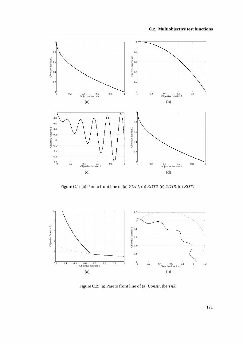
C.2. Multiobjective test functions
0 0.2 0.4 0.6 0.8 10
0.2
0.4
0.6
0.8
1
Objective function 1
Obj
ectiv
e fu
nctio
n 2
0 0.2 0.4 0.6 0.8 10
0.2
0.4
0.6
0.8
1
Objective function 1
Obj
ectiv
e fu
nctio
n 2
(a) (b)
0 0.2 0.4 0.6 0.8 1−0.8
−0.6
−0.4
−0.2
0
0.2
0.4
0.6
0.8
1
Objective function 1
Obj
ectiv
e fu
nctio
n 2
0 0.2 0.4 0.6 0.8 10
0.2
0.4
0.6
0.8
1
Objective function 1
Obj
ectiv
e fu
nctio
n 2
(c) (d)
Figure C.1: (a) Pareto front line of (a) ZDT1, (b) ZDT2, (c) ZDT3, (d) ZDT4.
0.3 0.4 0.5 0.6 0.7 0.8 0.9 10
2
4
6
8
10
Objective function 1
Obj
ectiv
e fu
nctio
n 2
0 0.2 0.4 0.6 0.8 1 1.20
0.2
0.4
0.6
0.8
1
1.2
Objective function 1
Obj
ectiv
e fu
nctio
n 2
(a) (b)
Figure C.2: (a) Pareto front line of (a) Constr, (b) Tnk.
171


APPENDIX D
Notebook charger: Preliminary study
and electronics
D.1 Energy chain
To determine the specifications of the CET system for the notebook charger, the whole system
has to be considered. Its energy chain is given in D.1. The different parts are the following
ones:
1. the grid;
2. the input rectifier;
3. the high frequency converter;
4. the coreless transformer;
5. the output rectifier;
6. the notebook battery (load).
In order to determine the specifications of the coreless transformer, each part (or function)
has to be analyzed separately. The following sections present the study that leads to the
establishment of specifications for the coreless transformer.

Appendix D. Notebook charger: Preliminary study and electronics
ACh-f
DC
RectifierHigh frequency
converter
Rectifier
AC
DC ACh-f
DC
Energysource
Resonant circuitand
magnetic system
Grids
Corelesstransformer
Load
Notebook
12 3
45
6
Figure D.1: Energy chain for the CET system of the notebook.
D.2 Charger and notebook specifications
D.2.1 Coils
The primary coil has to be integrated on the Alto platform in a way that it does not disturb
its conventional use. The secondary coil has to be integrated under the notebook. The only
restriction concerns the size of the coils that should not be larger than the one of the notebook,
that is approximately 240 mm by 160 mm.
The vertical distance (or airgap) between the primary and the secondary coil is 10 mm, due to
the thickness of the Alto platform and the integration of the primary coil.
D.2.2 Electrical requirements
As a first requirement, the battery charger has to draw its power directly from the grid. The
user should plug it and the CET has to be working.
Secondly, the notebook used for this project is a Dell Latitude C840. The original charger is
able to supply 20 V (DC) and 4.5 A (DC) to the notebook. Some measurements have been
performed while the computer was being charged. For these measurements, the screen was
set to a standard brightness and the CPU was not working. The measured voltage and current
drawn by the notebook oscillate periodically between two states:
174

D.2. Charger and notebook specifications
1. 18 V (DC), 3.2 A (DC) (during a few seconds)
2. 19.5 V (DC), 1.15 A (DC) (during a few seconds)
If the brightness of the screen is increased and the CPU is fully working, the current of the first
state can be increased (a maximal of 3.8 A (DC) has been measured). The load is automatically
managed by the internal electronics of the notebook. In brief, the goal is to realize a charger
that provides a stable voltage UL,DC of 20 V (DC) for a power up to 80 W, which offers a large
margin of security.
D.2.3 Input voltage of the coreless transformer
Fig. D.2 shows an electronic schematic of the primary side. The input voltage (AC) of the
coreless transformer is obtained in two steps.
Power bridge
T1
T3
T2
T4
UDC C1
L1
U1
CUgrid
Lin
Figure D.2: Electronic schematic from the grid to the primary coil. The secondaryside is not shown.
First, the grid voltage Ug r i d (240 V (AC rms), 50 Hz) is rectified by a full-bridge rectifier and a
smoothing capacitor. The rectifier used in this project is a Diotec KBU6G and the smoothing
capacitor is a standard one (C = 470 µF ). This gives the voltage UDC of 320 V (DC), obtained
as follows:
UDC = (Ug r i d
p2−2V j )0.95 ≈ 320 V (D.1)
where V j = 0.7 V is the forward voltage of the diodes. Here, a security margin of 5 % has been
used due to the fluctuation of the DC voltage, as outlined in Fig. D.3. Doing so has been
verified by measurement and shows a good agreement.
Secondly, a full-bridge converter (presented in section 5.1.3) allows to generate a HF voltage
U1 of 355 V (AC rms) on the primary coil. Theoretically, the converter applies a square wave
voltage to the primary coil. But the primary resonant capacitor has the effect of filtering the
higher harmonic voltages, which gives rise to a sine wave on the terminals of the primary coil.
175
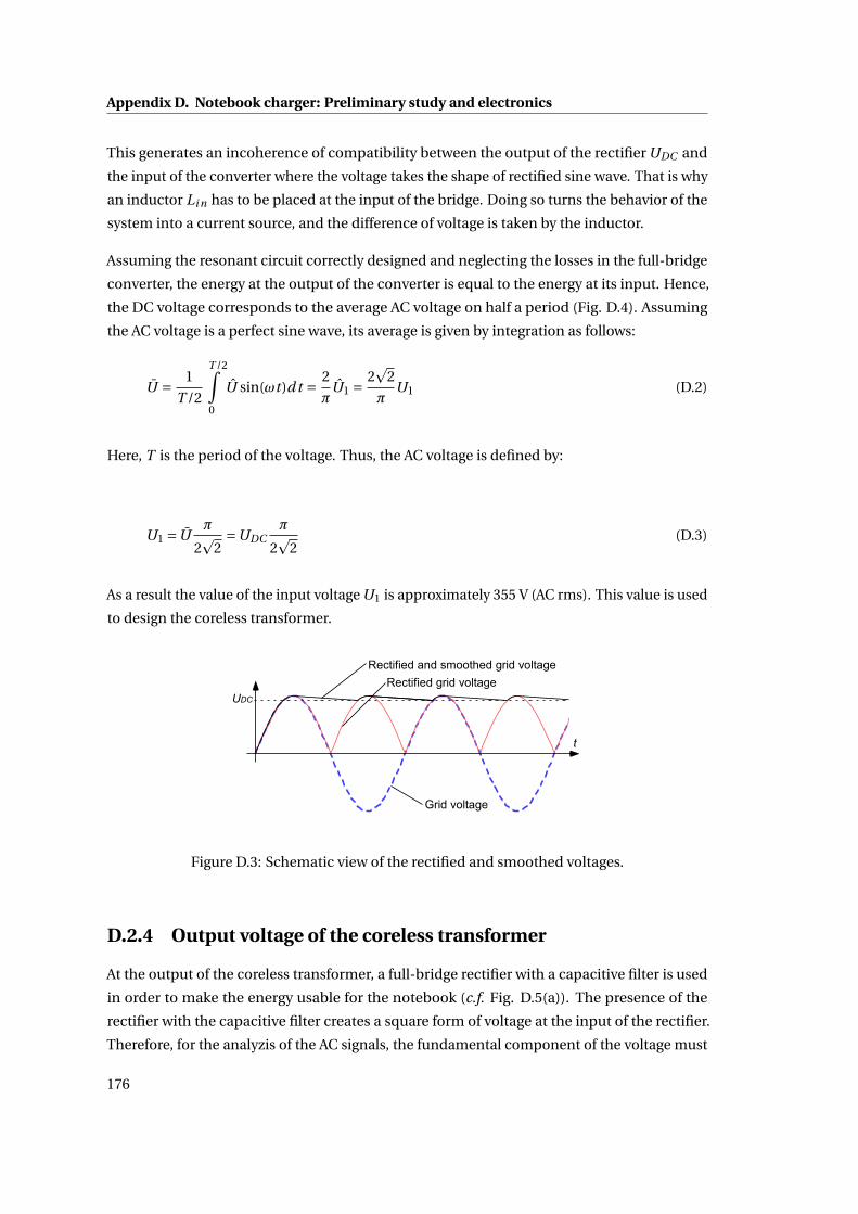
Appendix D. Notebook charger: Preliminary study and electronics
This generates an incoherence of compatibility between the output of the rectifier UDC and
the input of the converter where the voltage takes the shape of rectified sine wave. That is why
an inductor Li n has to be placed at the input of the bridge. Doing so turns the behavior of the
system into a current source, and the difference of voltage is taken by the inductor.
Assuming the resonant circuit correctly designed and neglecting the losses in the full-bridge
converter, the energy at the output of the converter is equal to the energy at its input. Hence,
the DC voltage corresponds to the average AC voltage on half a period (Fig. D.4). Assuming
the AC voltage is a perfect sine wave, its average is given by integration as follows:
U = 1
T /2
T /2∫0
U sin(ωt )d t = 2
πU1 = 2
p2
πU1 (D.2)
Here, T is the period of the voltage. Thus, the AC voltage is defined by:
U1 = Uπ
2p
2=UDC
π
2p
2(D.3)
As a result the value of the input voltage U1 is approximately 355 V (AC rms). This value is used
to design the coreless transformer.
UDC
t
Grid voltage
Rectified grid voltageRectified and smoothed grid voltage
Figure D.3: Schematic view of the rectified and smoothed voltages.
D.2.4 Output voltage of the coreless transformer
At the output of the coreless transformer, a full-bridge rectifier with a capacitive filter is used
in order to make the energy usable for the notebook (c.f. Fig. D.5(a)). The presence of the
rectifier with the capacitive filter creates a square form of voltage at the input of the rectifier.
Therefore, for the analyzis of the AC signals, the fundamental component of the voltage must
176

D.2. Charger and notebook specifications
UDC
t
Grid voltage
Rectified grid voltageRectified and smoothed grid voltage
UDC
t
Û1
Figure D.4: Schematic view of the AC voltage at the converter output.
be used [119]. But the rectifier changes the impedance of the load for the resonant circuit
because of the nonlinearity introduced by the rectifier. The resulted impedance formed by the
rectifier and the load itself can be modeled by an equivalent resistor as shown in Fig. D.5(b).
Its value is given by [46], [75]:
Req = 8
π2 RL (D.4)
With this, the computation of AC voltages and currents remains valid by taking the fundamen-
tal components of the signals and by loading the resonant circuit with the equivalent load
resistance. This leads to an equivalent load resistance Req of 4.6 Ω for the first state of the
supplying process (worst case). Furthermore the AC voltage required by the equivalent load is
given by:
UL,eq = 2p
2
πULDC (D.5)
By taking into account the voltage drop U j in the diodes, the necessary AC voltage that ensures
a DC voltage of 20 V (DC) to the notebook is:
UL,eq = 2p
2
πULDC +2U j (D.6)
In conclusion, the AC voltage UL,eq required at the output of the coreless transformer is 20 V
(AC rms).
D.2.5 Summary
In conclusion, Table 5.1 gives a summary of the different specifications for the coreless trans-
former.
177
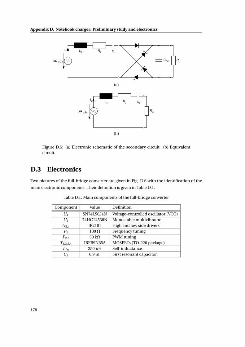
Appendix D. Notebook charger: Preliminary study and electronics
L2 R2 C2
RL
I2
jωL12IL1
L2 R2 C2
Req
I2
jωL12IL1
CDC
(a)
L2 R2 C2
RL
I2
jωL12IL1
L2 R2 C2
Req
I2
jωL12IL1
CDC
(b)
Figure D.5: (a) Electronic schematic of the secondary circuit. (b) Equivalentcircuit.
D.3 Electronics
Two pictures of the full-bridge converter are given in Fig. D.6 with the identification of the
main electronic components. Their definition is given in Table D.1.
Table D.1: Main components of the full-bridge converter
Component Value Definition
U1 SN74LS624N Voltage-controlled oscillator (VCO)U2 74HCT4538N Monostable multivibrator
U3,4 IR2101 High and low side driversP1 100Ω Frequency tuning
P2,3 50 kΩ PWM tuningT1,2,3,4 IRFB9N65A MOSFETs (TO-220 package)
Li n 250 µH Self-inductanceC1 6.9 nF First resonant capacitor.
178

D.3. Electronics
Lin
C1
P1,2,3
InputConnectors
OutputConnectors
5 V DC
12 V DC
U1,2
Power Circuit
U3,4T1,2
T3
T4
(a)
T1,2 T3,4Cooler
InputConnectors
OutputConnectors
(b)
Figure D.6: (a) Top view and (b) side view of the full-bridge converter.
179

Appendix D. Notebook charger: Preliminary study and electronics
A picture of the full-bridge rectifier is given in Fig. D.7 with the identification of the main
electronic components. Their definition is given in Table D.2.
AC Input
DC Output
C2
CDC
D1,2,3,4
Figure D.7: The output rectifier with the series compensation capacitor and thefilter capacitor.
Table D.2: Components used in the rectifier.
Component Value Definition
D1,2,3,4 SB1240 Schottky Barrier Rectifiers.C2 470 nF Second resonant capacitor.
CDC 1.68 µF Filter capacitor.
180

APPENDIX E
CET table: electronics
E.1 Primary coils array implementation
The main electronics used in the primary side and a portion of the primary coils array are
shown in Fig. E.1. The main components are then defined in Table E.1.
T1,...,6
T7,...,12
U1,...,6
Control DSPWires DC1,...,6DC7 DC8
R1,2,3 U7
Current EstimationCircuit Column LinesRow LinesC1,...,36 D1,...,36
Figure E.1: Photograph of the primary electronic circuit and a portion of theprimary coils array.

Appendix E. CET table: electronics
Table E.1: Description of the main components used in the primary circuit.
Component Value Definition
T1,...,6 IRF530N MOSFETs driving the column linesT7,...,12 IRF530N MOSFETs driving the row linesU1,...,6 IR2110 Low-side and high-side drivers
U7 - Part of the detection circuitR1,2,3 - Parts of the detection circuit
DC1,...,6 Traco TME 1212S 12 V/12 V DC/DC converter for the high-sidedrivers
DC7 Traco TEL 1210 2 Watts DC/DC converter with an output of 3.3 V.DC8 Traco TED 1222 2 Watts DC/DC converter with an output of ±15 V.
C1,...,36 Low ESR ceramic 100 nF Primary parallel compensation capacitors.D1,...,36 30BQ100 Shottky diodes.
Basically, the switch functions are achieved by using 12 MOSFET transistors that require
drivers to be activated. Therefore, 6 separate ICs (U1,...,6) are used, each of them containing
a low-side driver for the row switches and a high-side driver for the column switches. The
high frequency PWMs generated by the microcontroller are then routed to the input of the
low-side drivers while the logic signals for controlling the column switches are routed to the
high-side inputs. The 6 DC/DC converters DC1,...,6 are used to generate the high-side floating
supply voltage and the DC/DC converter DC7 is used to generate the logic supply voltage
(3.3 V) corresponding to the output level of the microcontroller. Furthermore, 36 capacitors
C1,...,36 are used as primary resonant for each coil, and 36 diodes are placed in series with each
primary coil and capacitor in order to prevent the current from flowing back into other coils.
E.2 Detection method implementation
The different electronic components used for the detection system are presented in Table E.2.
Table E.2: The main components used in the detection circuit.
Component Value Definition
U7 TL072CP Low-noise operational amplifier for the currentestimation circuit.
RS 0.1Ω SMS-R100-1.0 Shunt resistor.R1 10 kΩ Amplifier resistor.R2 22 kΩ Amplifier resistor.R3 100 kΩ Low-pass filter resistor.R4 1 kΩ Limiting current resistor.C1 3.3 nF Low-pass filter capacitor.
D1,2 BAT48 Small signal shottky diodes.
182

E.3. Secondary circuit implementation
E.3 Secondary circuit implementation
The different electronic components used in the secondary circuit are presented in Table E.3.
Table E.3: Description of the main components used in the primary circuit.
Component Value Definition
L22 25.45 µH Measured secondary coil self inductance.R2 0.95Ω Measured secondary coil resistance.C2 25.3 nF Secondary resonant capacitor.U1 LM2990T-5.0 Negative low dropout regulator.
D1,...,4 SB1240 Shottky diodes with a low forward voltage.CU 1 0.47 µF Electrolytic capacitor.CU 2 0.22 µF Electrolytic capacitor.
To supply the mouse and the keyboard, a linear adjustable regulator LM317 is used with the
right resistors configuration so as to obtain respectively 1.5 V (DC) and a 3 V (DC) at their
output.
183


Bibliography
[1] Alto picture. [Online], http://www.caron-informatique.fr/catalog/images/...cordless.jpg,June 2010.
[2] Alto picture. [Online], http://static.pcinpact.com/images/bd/news/33768-alto-logitech.jpg, June 2010.
[3] Car wireless charging by haloipt. [Online], http://www.haloipt.com/, September 2011.
[4] Contactless electric vehicle charging prototype by bmw and siemens. [On-line], http://techprezz.com/2011/04/bmw- and-siemens-introduces-induction-based-wireless-charging-ev-concept/, September 2011.
[5] Contactless energy transfer of the ecoupled table. [Online], http://ecoupled.com/,September 2011.
[6] Contactless energy transfer system for a small dockstation. [Online],http://www.hpwebos.com/us/products... .../accessories/touchstone-technology.html,September 2011.
[7] Inductive charging toothbrushes. [Online], http://www.oralb.com/, September 2011.
[8] Inductive powering mouse. [Online], http://www.a4tech.com/, September 2011.
[9] Logitech. [Online], http://www.logitech.com, September 2011.
[10] The maximum power transfer as a function of the coils size and the fre-quency with respect to the health restrictions recommanded by the in-ternational commission on non-ionizing radiation protection. [Online],http://www.wirelesspowerconsortium.com/technology/maximum-power-transfer-into-space.html, September 2011.
[11] The philips sonicare website. [Online], http://www.sonicare.com, September 2011.
[12] Powermat product line. [Online], http://www.powermateu.com/H, September 2011.
[13] The swissmetro website. [Online], http://www.swissmetro.ch, September 2011.
185

Bibliography
[14] Tesla’s experiments. [Online], http://www.neuronet.pitt.edu, September 2011.
[15] The westinghouse electric corporation website. [Online],http://www.westinghouse.com, September 2011.
[16] Wireless charging platform. [Online], http://www.qualcomm.com, September 2011.
[17] Wireless charging platform. [Online], http://www.mojomobility.com/, September 2011.
[18] The wireless power consortium. [Online], http://www.wirelesspowerconsortium.com/,September 2011.
[19] Witricity contactless system for electric vehicles. [Online],http://www.witricity.com/pages/ev-charging-system.html, September 2011.
[20] Cedrat website. [Online], http://www.cedrat.com/, January 2012.
[21] Genetic algorithm toolbox. [Online], http://www.mathworks.com/, January 2012.
[22] Inca3d from cedrat website. [Online], http://www.cedrat.com/InCa3D, August 2012.
[23] Vilfredo pareto’s life. [Online], http://en.wikipedia.org/wiki/VilfredoPareto, February2012.
[24] J. Achterberg, E. A. Lomonova, and J. de Boeij. Coil array structures compared forcontactless battery charging platform. Magnetics, IEEE Transactions on, 44(5):617–622,May 2008.
[25] A. Ahlbom, U. Bergqvist, J. H. Bernhardt, J. Cesarini, L. A. Court, M. Grandolfo, M. Hi-etanen, A. F. Mckinlay, M. H. Repacholi, D. H. Sliney, J. A. J. Stolwijk, M. L. Swicord,L. D. Szabo, M. Taki, T. S. Tenforde, H. P. Jammet, and R. Matthes. Guidelines for limit-ing exposure to time-varying electric, magnetic, and electromagnetic fields (up to 300GHz). International Commission on Non-Ionizing Radiation Protection. Health Phys,74(4):494–522, Apr. 1998.
[26] G. Antonini, A. Orlandi, and C. Paul. Internal impedance of conductors of rectangularcross section. Microwave Theory and Techniques, IEEE Transactions on, 47(7):979 –985,jul. 1999.
[27] A. Balakrishnan, W. Palmer, W. Joines, and T. Wilson. The inductance of planar structures.In Applied Power Electronics Conference and Exposition, 1993. APEC ’93. ConferenceProceedings 1993., Eighth Annual, pages 912 –921, mar 1993.
[28] S. Bandyopadhyay, S. Saha, U. Maulik, and K. Deb. A simulated annealing-based multi-objective optimization algorithm: Amosa. Evolutionary Computation, IEEE Transactionson, 12(3):269 –283, june 2008.
[29] T. Bieler, M. Perrottet, V. Nguyen, and Y. Perriard. Contactless power and informationtransmission. Industry Applications, IEEE Transactions on, 38(5):1266–1272, Sep/Oct2002.
186

Bibliography
[30] A. Bourquard. Optimisation d’un instrument chirurgical ultrasonique par algorithmesgenetique. Semester project, Ecole Polytechnique Federale de Lausanne (EPFL), 2008.
[31] H. Chan, K. Cheng, and D. Sutanto. A simplified neumann’s formula for calculation ofinductance of spiral coil. In Power Electronics and Variable Speed Drives, 2000. EighthInternational Conference on (IEE Conf. Publ. No. 475), pages 69 –73, 2000.
[32] D. K. Cheng. Field and Wave Electromagnetics. The Addison-Wesley series in electricalengineering. Addison-Wesley, 1989.
[33] B. Choi and J. Nho. Contactless energy transfer using planar printed circuit boardwindings. Electronics Letters, 37(16):1007–1009, 2 Aug 2001.
[34] B. Choi, J. Nho, H. Cha, T. Ahn, and S. Choi. Design and implementation of low-profile contactless battery charger using planar printed circuit board windings as energytransfer device. Industrial Electronics, IEEE Transactions on, 51(1):140–147, Feb. 2004.
[35] H. Chung and M. Pong. Effect of switching frequency and number of winding layers oncopper loss of an inductor. In Power Electronics and Motion Control Conference, 2000.Proceedings. IPEMC 2000. The Third International, volume 3, pages 1312 –1317 vol.3,2000.
[36] K. Coperich, A. Ruehli, and A. Cangellaris. Enhanced skin effect for partial-elementequivalent-circuit (peec) models. Microwave Theory and Techniques, IEEE Transactionson, 48(9):1435 –1442, sep 2000.
[37] J. de Boeij, E. Lomonova, J. Duarte, and A. Vandenput. Contactless energy transfer toa moving load part ii: Simulation of electrical and mechanical transient. IndustrialElectronics, 2006 IEEE International Symposium on, 2:745–750, July 2006.
[38] J. de Boeij, E. Lomonova, and A. Vandenput. Contactless energy transfer to a movingload part i: Topology synthesis and fem simulation. Industrial Electronics, 2006 IEEEInternational Symposium on, 2:739–744, July 2006.
[39] J. de Boeij, E. A. Lomonova, and A. J. A. Vandenput. Optimization of contactless planaractuator with manipulator. Magnetics, IEEE Transactions on, 44(6):1118–1121, June2008.
[40] K. Deb and M. Goyal. A Combined Genetic Adaptive Search (GeneAS) for EngineeringDesign. Computer Science and Informatics, 26:30–45, 1996.
[41] K. Deb, A. Pratap, S. Agarwal, and T. Meyarivan. A fast elitist multi-objective geneticalgorithm: Nsga-ii. IEEE Transactions on Evolutionary Computation, 6:182–197, 2000.
[42] T. Demeester and D. de Zutter. Applications of the dirichlet-to-neumann boundaryoperator in transmission line modeling. In Electromagnetic Compatibility, 2009 20thInternational Zurich Symposium on, pages 25 –28, jan. 2009.
[43] T. Demeester and D. De Zutter. Internal impedance of composite conductors witharbitrary cross section. Electromagnetic Compatibility, IEEE Transactions on, 51(1):101–107, feb. 2009.
187

Bibliography
[44] D. DeZutter and L. Knockaert. Skin effect modeling based on a differential surface ad-mittance operator. Microwave Theory and Techniques, IEEE Transactions on, 53(8):2526– 2538, aug. 2005.
[45] R. M. Dickinson. Wireless power transmission technology state of the art the first billbrown lecture. Acta Astronautica, 53(4-10):561–570, 2003.
[46] A. Ecklebe and A. Lindemann. Analysis and design of a contactless energy transmissionsystem with flexible inductor positioning for automated guided vehicles. IEEE IndustrialElectronics, IECON 2006 - 32nd Annual Conference on, pages 1721–1726, Nov. 2006.
[47] M. Enohnyaket and J. Ekman. Peec models for air-core reactors modeling skin andproximity effects. In Power Electronics Specialists Conference, 2007. PESC 2007. IEEE,pages 3034 –3038, june 2007.
[48] H. Eskandari and C. D. Geiger. A fast pareto genetic algorithm approach for solvingexpensive multiobjective optimization problems. Journal of Heuristics, 14(3):203–241,June 2008.
[49] A. Esser. Contactless charging and communication for electric vehicles. IndustryApplications Magazine, IEEE, 1(6):4 –11, nov/dec 1995.
[50] C. Fernandez, O. Garcia, R. Prieto, J. Cobos, S. Gabriels, and G. Van Der Borght. Designissues of a core-less transformer for a contact-less application. Applied Power ElectronicsConference and Exposition, 2002. APEC 2002. Seventeenth Annual IEEE, 1:339–345 vol.1,2002.
[51] C. Fernandez, R. Prieto, O. Garcia, P. Herranz, J. Cobos, and J. Uceda. Modelling core-lesshigh frequency transformers using finite element analysis. Power Electronics SpecialistsConference, 2002. pesc 02. 2002 IEEE 33rd Annual, 3:1260–1265 vol.3, 2002.
[52] J. Fernandez Lopez. Modeling and optimization of ultrasonic linear motors. PhD thesis,Ecole Polytechnique Federale de Lausanne (EPFL), 2006.
[53] A. Garcia, J. Carrasco, J. Soto, F. Maganto, and C. Morón. A method for calculatingthe magnetic field produced by a coil of any shape. Sensors and Actuators A: Physical,91(1-2):230 – 232, 2001. Third European Conference on Magnetic Sensors & Actuators.
[54] O. Gatous and J. Pissolato. Frequency-dependent skin-effect formulation for resistanceand internal inductance of a solid cylindrical conductor. Microwaves, Antennas andPropagation, IEE Proceedings -, 151(3):212 – 216, 2004.
[55] P. Germano and M. Jufer. Contactless power transmission: Frequency tuning by a maxi-mum power tracking method. EPE ’97, 7th European Conference on power electronicsand applications, Trondheim, IV:693–697, September 1997.
[56] P. Germano, N. Macabrey, and M. Jufer. Contactless power transmission: Linear posi-tioning of the moving element. Technical report, Swiss Federal Institute of Technology,Lausanne (EPFL) DE-LEME / ELG, 1998.
188
Bibliography
[57] P. Germano, I. Stefanini, and Y. Perriard. Stimulation colique pour le traitement destroubles de la motilité - projet colostim. Technical report, LAI-CHUV, 2007.
[58] P. Germano, I. Stefanini, and Y. Perriard. Contactless system dedicated to colic stimula-tion. ICEM 2008, Vilamoura, Portugal, 2008.
[59] D. E. Goldberg. Genetic Algorithm in Search, Optimization, and Machine Learning.Addison-Wesley, New York, 1989.
[60] H. Greenhouse. Design of planar rectangular microelectronic inductors. Parts, Hybrids,and Packaging, IEEE Transactions on, 10(2):101–109, Jun 1974.
[61] J. Gyselinck and F. Robert. Frequency- and time-domain homogenization of windingsin two-dimensional finite-element models. In Power Electronics and Applications, 2005European Conference on, pages 10 pp. –P.10, 0-0 2005.
[62] K. Hatanaka, F. Sato, H. Matsuki, S. Kikuchi, J. Murakami, M. Kawase, and T. Satoh. Powertransmission of a desk with a cord-free power supply. Magnetics, IEEE Transactions on,38(5):3329 – 3331, sep. 2002.
[63] T. J. Higgins. Formulas for the geometric mean distances of rectangular areas and ofline segments. Journal of Applied Physics, 14:188–195, 1943.
[64] J. H. Holland. Adaptation in Natural and Artificial Systems. University of Michigan Press,1975.
[65] S. R. H. Hoole. Computer-Aided Analysis and Design of Electromagnetic Devices. Elsevier,New York, 1989.
[66] A. Hu, W. Ma, and Z. Zhao. New numerical methods of computing internal inductanceof conductors of rectangular cross section. In Electromagnetic Compatibility and 19thInternational Zurich Symposium on Electromagnetic Compatibility, 2008. APEMC 2008.Asia-Pacific Symposium on, pages 674 –677, may 2008.
[67] S. Hui and W. Ho. A new generation of universal contactless battery charging platformfor portable consumer electronic equipment. Power Electronics, IEEE Transactions on,20(3):620–627, May 2005.
[68] W. Hurley and M. Duffy. Calculation of self and mutual impedances in planar magneticstructures. Magnetics, IEEE Transactions on, 31(4):2416–2422, Jul 1995.
[69] W. Hurley and M. Duffy. Calculation of self- and mutual impedances in planar sandwichinductors. Magnetics, IEEE Transactions on, 33(3):2282–2290, May 1997.
[70] O. A. Jadaan, L. Rajamani, and C. Rao. Improved selection operator for ga. Journal ofTheoretical and Applied Information Technology, 2005-2008.
[71] H. E. S. Jr., J. C. Schuder, and J. W. Mackenzie. Energy transport through tissue byinductive coupling. The American Journal of Surgery, 114(1):87 – 94, 1967.
[72] P. Kaelo and M. Ali. Integrated crossover rules in real coded genetic algorithms. EuropeanJournal of Operational Research, 176(1):60 – 76, 2007.
189

Bibliography
[73] M. Klauz and D. Dorrell. Eddy current effects in a switched reluctance motor. Magnetics,IEEE Transactions on, 42(10):3437 –3439, oct. 2006.
[74] J. Knowles and D. Corne. The pareto archived evolution strategy: a new baselinealgorithm for pareto multiobjective optimisation. In Evolutionary Computation, 1999.CEC 99. Proceedings of the 1999 Congress on, volume 1, pages 3 vol. (xxxvii+2348), 1999.
[75] R. Laouamer, J. P. Ferrieux, H. Benqassmi, O. Normand, and N. Buchheit. A comparisonof resonant converter topologies with three and four energy storage elements for auto-matic inductive charging application. Electric Machines and Power Systems, 27:221–236,March 1999.
[76] J. Li, Y. Shi, Z. Niu, and D. Zhou. Modeling, simulation and optimization design of pcbplanar transformer. In Electrical Machines and Systems, 2005. ICEMS 2005. Proceedingsof the Eighth International Conference on, volume 3, pages 1736 –1739 Vol. 3, sept. 2005.
[77] X. Liu and S. Hui. Optimal design of a hybrid winding structure for planar contactlessbattery charging platform. Power Electronics, IEEE Transactions on, 23(1):455–463, Jan.2008.
[78] X. Liu and S. Hui. Simulation study and experimental verification of a universal contact-less battery charging platform with localized charging features. Power Electronics, IEEETransactions on, 22(6):2202–2210, Nov. 2007.
[79] S. Llorente, F. Monterde, J. Burdio, and J. Acero. A comparative study of resonant invertertopologies used in induction cookers. In Applied Power Electronics Conference andExposition, 2002. APEC 2002. Seventeenth Annual IEEE, volume 2, pages 1168 –1174vol.2, 2002.
[80] E. Lou, N. Durdle, V. Raso, and D. Hill. Measurement of the magnetic field in the near-field region and self-inductance in free space due to a multiturn square-loop. Science,Measurement and Technology, IEE Proceedings -, 144(6):252 –256, nov 1997.
[81] Y. Louvrier. Etude et optimizsation multicritère d’un convertisseur DC-DC à canauxmultiples entrelacés. PhD thesis, Ecole Polytechnique Federale de Lausanne (EPFL),2010.
[82] N. Macabrey. Alimentation et guidage linéaire sans contact. PhD thesis, Ecole Polytech-nique Federale de Lausanne (EPFL), 1998.
[83] V. Marian, C. Vollaire, B. Allard, and J. Verdier. Low power rectenna topologies formedium range wireless energy transfer. In Power Electronics and Applications (EPE2011), Proceedings of the 2011-14th European Conference on, pages 1 –10, 30 2011-sept.1 2011.
[84] J. Maridor. Design, optimization and sensorless control of a linear actuator. PhD thesis,Ecole Polytechnique Federale de Lausanne (EPFL), 2011.
[85] J. Maridor, M. Markovic, Y. Perriard, and D. Ladas. Optimization design of a linearactuator using a genetic algorithm. In Electric Machines and Drives Conference, 2009.IEMDC ’09. IEEE International, pages 1776 –1781, may 2009.
190
Bibliography
[86] H. Matsuki, M. Shiiki, K. Murakami, K. Nadehara, and T. Yamamoto. Flexible tran-scutaneous transformer for artificial heart system. Magnetics, IEEE Transactions on,26(5):1548 –1550, sep 1990.
[87] H. Matsuki, M. Shiiki, K. Murakami, and T. Yamamoto. Investigation of coil geometry fortranscutaneous energy transmission for artificial heart. Magnetics, IEEE Transactionson, 28(5):2406–2408, Sep 1992.
[88] P. Meyer, P. Germano, M. Markovic, and Y. Perriard. Design of a contactless energytransfer system for desktop peripherals. In Energy Conversion Congress and Exposition(ECCE), 2010 IEEE, pages 2253 –2258, 2010.
[89] P. Meyer, P. Germano, M. Markovic, and Y. Perriard. Design of a contactless energy-transfer system for desktop peripherals. Industry Applications, IEEE Transactions on,47(4):1643 –1651, july-aug. 2011.
[90] P. Meyer, P. Germano, and Y. Perriard. Modelling and design of a contactless energytransfer system for a notebook battery charger. In Electrical Machines (ICEM), 2010 XIXInternational Conference on, pages 1 –6, 2010.
[91] P. Meyer, P. Germano, and Y. Perriard. Contactless energy transfer system for computerperipherals. In Power Electronics and Applications (EPE 2011), Proceedings of the 2011-14th European Conference on, pages 1 –10, 30 2011-sept. 1 2011.
[92] Z. Michalewicz. A survey of constraint handling techniques in evolutionary computationmethods. In Proceedings of the 4th Annual Conference on Evolutionary Programming,pages 135–155, 1995.
[93] W. Mingli and F. Yu. Numerical calculations of internal impedance of solid and tubularcylindrical conductors under large parameters. Generation, Transmission and Distribu-tion, IEE Proceedings-, 151(1):67 – 72, 2004.
[94] S. Mohan, M. del Mar Hershenson, S. Boyd, and T. Lee. Simple accurate expressions forplanar spiral inductances. Solid-State Circuits, IEEE Journal of, 34(10):1419–1424, Oct1999.
[95] P. C. Pendharkar and J. A. Rodger. An empirical study of impact of crossover operatorson the performance of non-binary genetic algorithm based neural approaches forclassification. Comput. Oper. Res., 31:481–498, April 2004.
[96] A. Petrowski. A clearing procedure as a niching method for genetic algorithms. InEvolutionary Computation, 1996., Proceedings of IEEE International Conference on,pages 798 –803, may 1996.
[97] B. D. Popovic. Introductory Engineering Electromagnetics. Addison-Wesley, 1971.
[98] D. Porto. Design Methodology and Numerical Optimization of Ultrasonic Transducersfor Spinal Surgery. PhD thesis, Ecole Polytechnique Federale de Lausanne (EPFL), 2009.
[99] D. Porto, A. Bourquard, and Y. Perriard. Genetic algorithm optimization for a surgicalultrasonic transducer. In Ultrasonics Symposium, 2008. IUS 2008. IEEE, pages 1457–1460, nov. 2008.
191

Bibliography
[100] P. Ragot. Modélisation analytique multiphysique pour la conception optimale de mo-teurs synchrones à aimants permanents. PhD thesis, Ecole Polytechnique Federale deLausanne (EPFL), 2008.
[101] E. A. Rose, A. C. Gelijns, A. J. Moskowitz, D. F. Heitjan, L. W. Stevenson, W. Dembitsky,J. W. Long, D. D. Ascheim, A. R. Tierney, R. G. Levitan, J. T. Watson, N. S. Ronan, P. A.Shapiro, R. M. Lazar, L. W. Miller, L. Gupta, O. H. Frazier, P. Desvigne-Nickens, M. C. Oz,V. L. Poirier, and P. Meier. Long-term use of a left ventricular assist device for end-stageheart failure. New England Journal of Medicine, 345(20):1435–1443, 2001.
[102] B. Sareni and L. Krahenbuhl. Fitness sharing and niching methods revisited. Evolution-ary Computation, IEEE Transactions on, 2(3):97–106, Sept. 1998.
[103] F. Sato, H. Matsuki, S. Kikuchi, T. Seto, T. Satoh, H. Osada, and K. Seki. A new meandertype contactless power transmission system-active excitation with a characteristics ofcoil shape. Magnetics, IEEE Transactions on, 34(4):2069–2071, Jul 1998.
[104] F. Sato, J. Murakami, H. Matsuki, S. Kikuchi, K. Harakawa, and T. Satoh. Stable energytransmission to moving loads utilizing new clps. Magnetics, IEEE Transactions on,32(5):5034–5036, Sep 1996.
[105] T. Sato, F. Sato, and H. Matsuki. New functional electrical system using magnetic coilsfor power transmission and control signal detection. Magnetics, IEEE Transactions on,37(4):2925 –2928, jul 2001.
[106] T. Schaffter. Optimisation d’un moteur synchrone à l’aide des algorithmes génétiques.Semester project, Ecole Polytechnique Federale de Lausanne (EPFL), 2007.
[107] H. Shiroyama, H. Matsuo, and Y. Ishizuka. Quasi-resonant converter with dividedresonant capacitor on primary and secondary side. In Telecommunications EnergyConference, 2009. INTELEC 2009. 31st International, pages 1 –6, oct. 2009.
[108] C. Silva and E. B. Jr. Genetic algorithm development for multi-objective optimization ofbatch free-radical polymerization reactors. Computers & Chemical Engineering,27(8 - 9):1329 – 1344, 2003.
[109] P. Silvester. Modern Electromagnetic Fields. Prentice-Hall, Inc., Englewood Cliffs, N.J.,1968.
[110] A. Sinclair and J. Ferreira. Analysis and design of transmission-line structures by meansof the geometric mean distance. In AFRICON, 1996., IEEE AFRICON 4th, volume 2,pages 1062 –1065 vol.2, Sept. 1996.
[111] A. Sokolov and D. Whitley. Unbiased tournament selection. In Proceedings of the 2005conference on Genetic and evolutionary computation, GECCO ’05, pages 1131–1138, NewYork, NY, USA, 2005. ACM.
[112] C. Sonntag. Contactless Energy Transfer Platform using Air-cored Planar Inductors. PhDthesis, Eindhoven University of Technology, 2010.
192

Bibliography
[113] C. Sonntag, E. Lomonova, and J. Duarte. Implementation of the neumann formula forcalculating the mutual inductance between planar pcb inductors. In Electrical Machines,2008. ICEM 2008. 18th International Conference on, pages 1 –6, 2008.
[114] C. Sonntag, E. Lomonova, and J. Duarte. Variable-phase contactless energy transferdesktop part i: Design. pages 4460 –4465, oct. 2008.
[115] C. Sonntag, E. Lomonova, J. Duarte, and A. Vandenput. Specialized receivers for three-phase contactless energy transfer desktop applications. Power Electronics and Applica-tions, 2007 European Conference on, pages 1–11, 2-5 Sept. 2007.
[116] N. Srinivas and K. Deb. Multiobjective optimization using nondominated sorting ingenetic algorithms. Evolutionary Computation, 2:221–248, 1994.
[117] I. Stefanini. Méthodologie de conception et optimisation d’actionneurs intégrés sans fer.PhD thesis, Ecole Polytechnique Federale de Lausanne (EPFL), 2006.
[118] I. Stefanini, M. Markovic, and Y. Perriard. 3d inductance and impedance determinationtaking skin effect into account. In Electric Machines and Drives, 2005 IEEE InternationalConference on, pages 74 –79, May 2005.
[119] R. Steigerwald. A comparison of half-bridge resonant converter topologies. PowerElectronics, IEEE Transactions on, 3(2):174 –182, Apr. 1988.
[120] O. Stielau and G. Covic. Design of loosely coupled inductive power transfer systems.Power System Technology, 2000. Proceedings. PowerCon 2000. International Conferenceon, 1:85–90 vol.1, 2000.
[121] R. Suresh and K. Mohanasundaram. Pareto archived simulated annealing for permu-tation flow shop scheduling with multiple objectives. In Cybernetics and IntelligentSystems, 2004 IEEE Conference on, volume 2, pages 712 –717, 2004.
[122] M. Tanaka, H. Watanabe, Y. Furukawa, and T. Tanino. Ga-based decision support systemfor multicriteria optimization. In Systems, Man and Cybernetics, 1995. Intelligent Systemsfor the 21st Century., IEEE International Conference on, volume 2, pages 1556 –1561 vol.2,oct 1995.
[123] S. Tang, S. Hui, and H.-H. Chung. Characterization of coreless printed circuit board(pcb) transformers. Power Electronics, IEEE Transactions on, 15(6):1275–1282, Nov 2000.
[124] D. Thrimawithana and U. Madawala. A three-phase bi-directional ipt system for contact-less charging of electric vehicles. In Industrial Electronics (ISIE), 2011 IEEE InternationalSymposium on, pages 1957 –1962, june 2011.
[125] C.-S. Wang, G. Covic, and O. Stielau. Power transfer capability and bifurcation phenom-ena of loosely coupled inductive power transfer systems. Industrial Electronics, IEEETransactions on, 51(1):148–157, Feb. 2004.
[126] C.-S. Wang, G. Covic, and O. Stielau. Investigating an lcl load resonant inverter for induc-tive power transfer applications. Power Electronics, IEEE Transactions on, 19(4):995–1002,July 2004.
193
Bibliography
[127] C.-S. Wang, O. Stielau, and G. Covic. Design considerations for a contactless electricvehicle battery charger. Industrial Electronics, IEEE Transactions on, 52(5):1308–1314,Oct. 2005.
[128] R.-L. Wang and K. Okazaki. An improved genetic algorithm with conditional geneticoperators and its application to set-covering problem. Soft Computing - A Fusion ofFoundations, Methodologies and Applications, 11:687–694, 2007. 10.1007/s00500-006-0131-1.
[129] H. Wu, A. Hu, P. Si, D. Budgett, C. Tung, and S. Malpas. A push-pull resonant converterwith dual coils for transcutaneous energy transfer systems. In Industrial Electronics andApplications, 2009. ICIEA 2009. 4th IEEE Conference on, pages 1051 –1056, may 2009.
[130] W. Zhong, X. Liu, and S. Hui. Analysis on a single-layer winding array structure for con-tactless battery charging systems with free-positioning and localized charging features.In Energy Conversion Congress and Exposition (ECCE), 2010 IEEE, pages 658 –665, 2010.
[131] W. Zhong, X. Liu, and S. Hui. A novel single-layer winding array and receiver coilstructure for contactless battery charging systems with free-positioning and localizedcharging features. Industrial Electronics, IEEE Transactions on, 58(9):4136 –4144, sept.2011.
[132] E. Zitzler, K. Deb, and L. Thiele. Comparison of Multiobjective Evolutionary Algorithms:Empirical Results. Evolutionary Computation, 8:173–195, 2000.
[133] E. Zitzler and L. Thiele. Multiobjective evolutionary algorithms: a comparative casestudy and the strength pareto approach. Evolutionary Computation, IEEE Transactionson, 3(4):257 –271, nov 1999.
194

Curriculum Vitae
Pascal MEYER
Born July 10, 1984
Swiss Citizen
Studies and professional experience
2008-to date Teaching assistant and Ph.D. student at the Integrated Actuators
Laboratory (LAI), Ecole Polytechnique Fédérale de Lausanne
(EPFL), Switzerland.
2003-2008 Master of Science in Microengineering, Ecole Polytechnique
Fédérale de Lausanne (EPFL), Switzerland.
1998-2003 High School Diploma in Latin/Sciences, Saint-Maurice, Switzer-
land
Publications
P. Meyer, P. Germano, and Y. Perriard. Modelling and design of a contactless energy transfer system for
a notebook battery charger. In Electrical Machines (ICEM), 2010 XIX International Conference on, pages
1-6, 2010.
P. Meyer, P. Germano, M. Markovic, and Y. Perriard. Design of a contactless energy transfer system for
desktop peripherals. In Energy Conversion Congress and Exposition (ECCE), 2010 IEEE, pages 2253-2258,
2010.
P. Meyer, P. Germano, M. Markovic, and Y. Perriard. Design of a contactless energy transfer system for
desktop peripherals. Industry Applications, IEEE Transactions on, 47(4):1643-1651, july-aug. 2011.
P. Meyer and Y. Perriard. Skin and proximity effects for coreless transformers. In Electrical Machines
and Systems (ICEMS), 2011 International Conference on, pages 1-5, aug. 2011.
P. Meyer, P. Germano, and Y. Perriard. Contactless energy transfer system for computer peripherals. In
Power Electronics and Applications (EPE 2011), Proceedings of the 2011- 14th European Conference on,
pages 1-10, 30 2011-sept. 1 2011.
P. Meyer, P. Germano, and Y. Perriard. FEM modeling of skin and proximity effects for coreless trans-
formers. To appear in Electrical Machines and Systems (ICEMS), 2012 International Conference on.