Embed Size (px)
Citation preview
IEEE MQ: WIMNACT-45
Takumi Ohashi1*, Kohei Suda2, Seiya Ishihara2, Naomi Sawamoto2, Shimpei Yamaguchi1,Kentaro Matsuura1, Kuniyuki Kakushima1, Nobuyuki Sugii1, Akira Nishiyama1,
Yoshinori Kataoka1, Kenji Natori1, Kazuo Tsutsui1, Hiroshi Iwai1, Atsushi Ogura2, and Hitoshi Wakabayashi1
1Tokyo Institute of Technology2Meiji University
MoS2 film thinning on high-temperature sputtering for enhancement-mode
nMOSFETs

More Moore, More than Moore
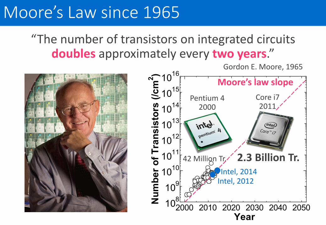
Moore’s Law since 1965“The number of transistors on integrated circuits
doubles approximately every two years.”Gordon E. Moore, 1965
2000 2010 2020 2030 2040 2050108109
1010101110121013101410151016
Year
Num
ber o
f Tra
nsis
tors
(/cm
2 )
Moore’s law slope
Intel, 2014Intel, 2012
42 Million Tr. 2.3 Billion Tr.
Pentium 42000
Core i72011
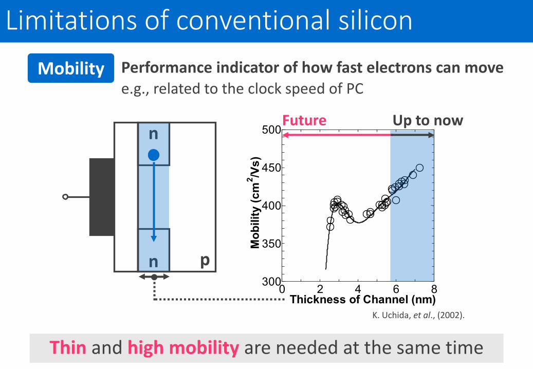
Limitations of conventional siliconMobility Performance indicator of how fast electrons can move
e.g., related to the clock speed of PC
0 2 4 6 8300
350
400
450
500
Thickness of Channel (nm)
Mob
ility
(cm
2 /Vs)
K. Uchida, et al., (2002).
Up to nowFuturen
n p
Thin and high mobility are needed at the same time
Our solution- 2D material with sputtering -
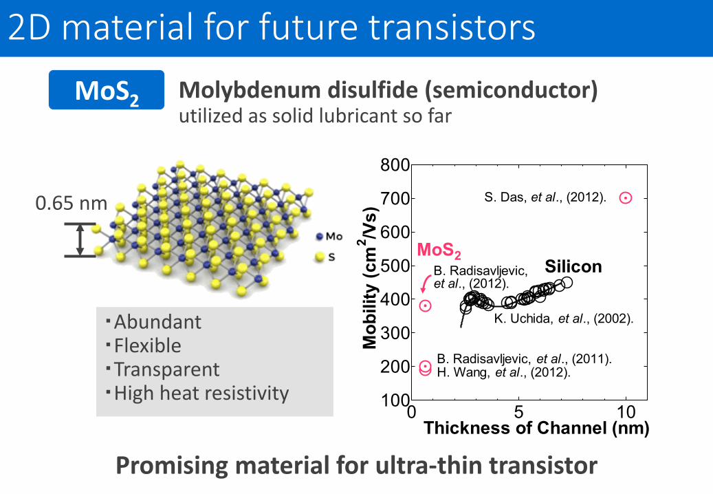
2D material for future transistorsMolybdenum disulfide (semiconductor)utilized as solid lubricant so far
MoS2
Promising material for ultra-thin transistor
・Abundant・Flexible・Transparent・High heat resistivity
0 5 10100
200
300
400
500
600
700
800
Thickness of Channel (nm)
Mob
ility
(cm
2 /Vs)
MoS2Silicon
B. Radisavljevic, et al., (2011).H. Wang, et al., (2012).
S. Das, et al., (2012).
B. Radisavljevic,
K. Uchida, et al., (2002).
et al., (2012).
0.65 nm
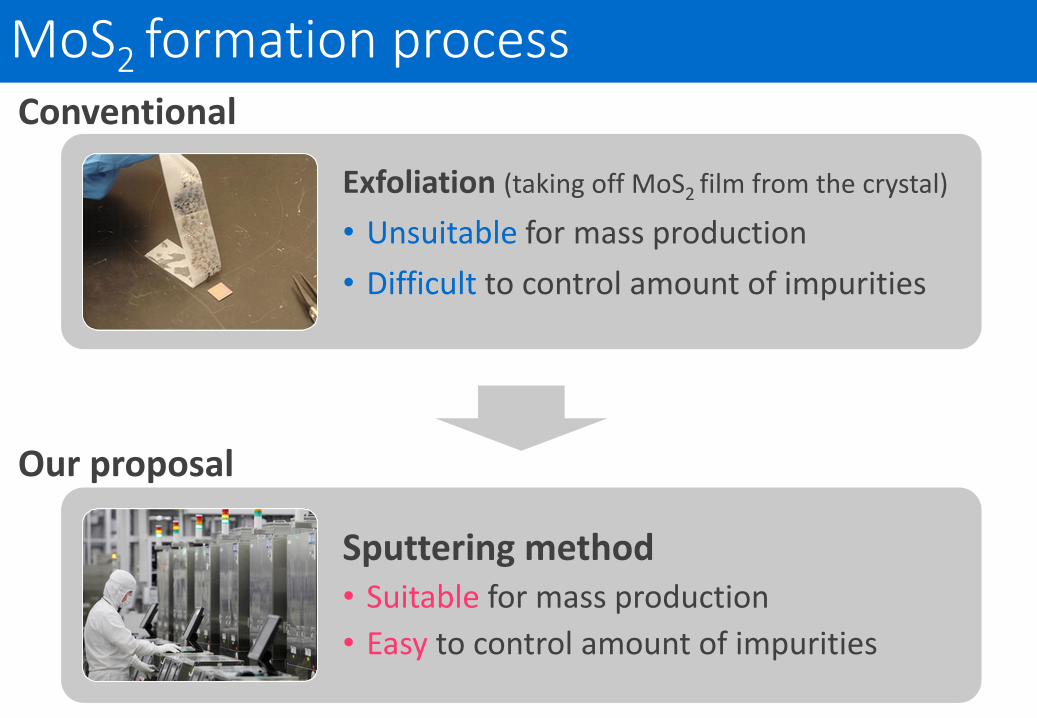
MoS2 formation process
Exfoliation (taking off MoS2 film from the crystal)
• Unsuitable for mass production• Difficult to control amount of impurities
Sputtering method• Suitable for mass production• Easy to control amount of impurities
Conventional
Our proposal

Current achievements
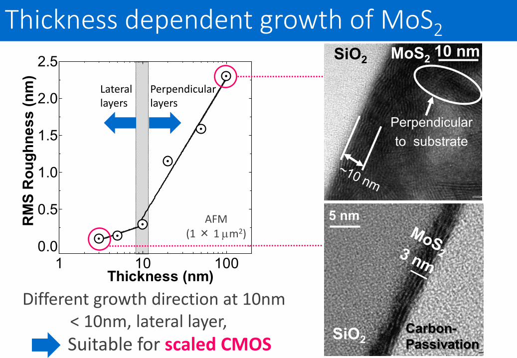
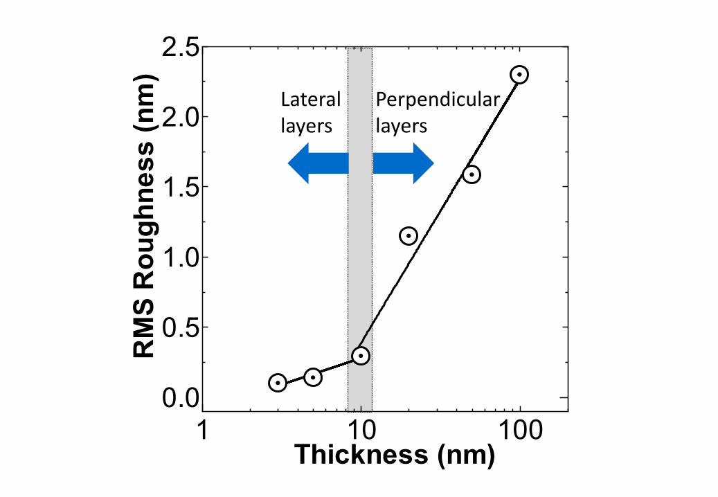
Thickness dependent growth of MoS2
1 10 1000.0
0.5
1.0
1.5
2.0
2.5
Thickness (nm)
RM
S R
ough
ness
(nm
)
Lateral layers
Perpendicularlayers
10 nmSiO2 MoS2
Perpendicularto substrate
5 nm
SiO2Carbon-Passivation
AFM(1 × 1 µm2)
Suitable for scaled CMOS
Different growth direction at 10nm< 10nm, lateral layer,
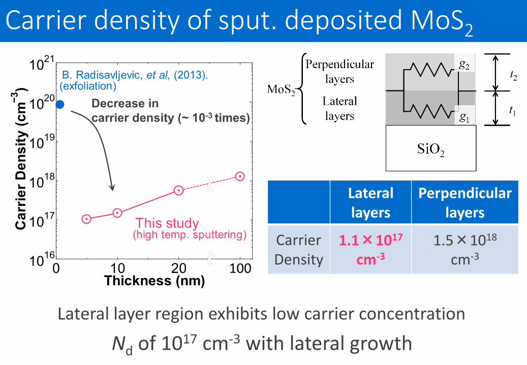
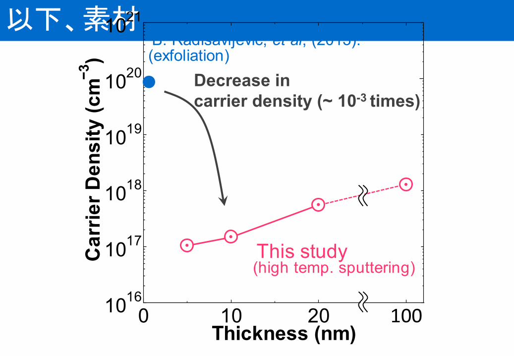
Carrier density of sput. deposited MoS2
0 10 20 301016
1017
1018
1019
1020
1021
Thickness (nm)
Car
rier D
ensi
ty (c
m−3
)
(high temp. sputtering)
B. Radisavljevic, et al, (2013).
This study
(exfoliation)
100
Decrease in carrier density (~ 10-3 times)
Laterallayers
Perpendicularlayers
CarrierDensity
1.1×10¹⁷
cm-31.5×10¹⁸
cm-3
Lateral layer region exhibits low carrier concentration
Nd of 1017 cm-3 with lateral growth
Future direction&
Conclusion
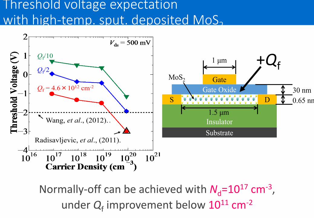
Threshold voltage expectation with high-temp. sput. deposited MoS2
H. Wang, et al, (2012).
B. Radisavljevic, et al, (2011).
Qf = 4.6×1012 cm-2
Qf/2
Qf/10
Wang, et al., (2012).
Radisavljevic, et al., (2011).
Gate OxideS D
InsulatorSubstrate
Gate
0.65 nm30 nm
1.5 μm
1 μm
MoS2
+Qf
Normally-off can be achieved with Nd=1017 cm-3, under Qf improvement below 1011 cm-2
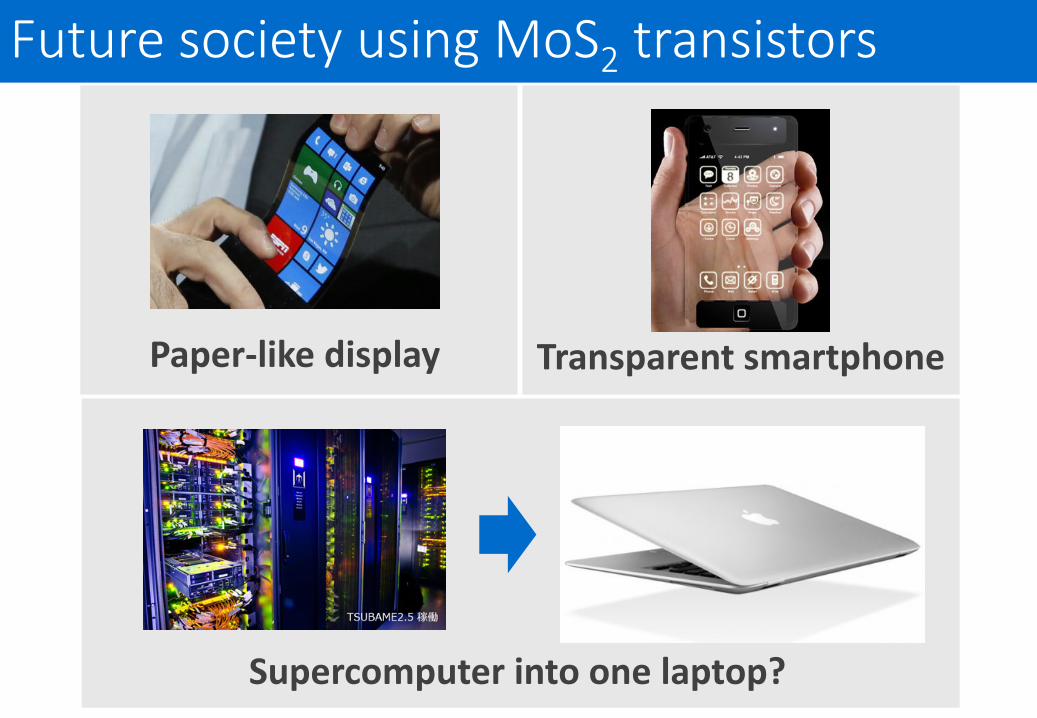
Future society using MoS2 transistors
Paper-like display Transparent smartphone
Supercomputer into one laptop?
Conclusion
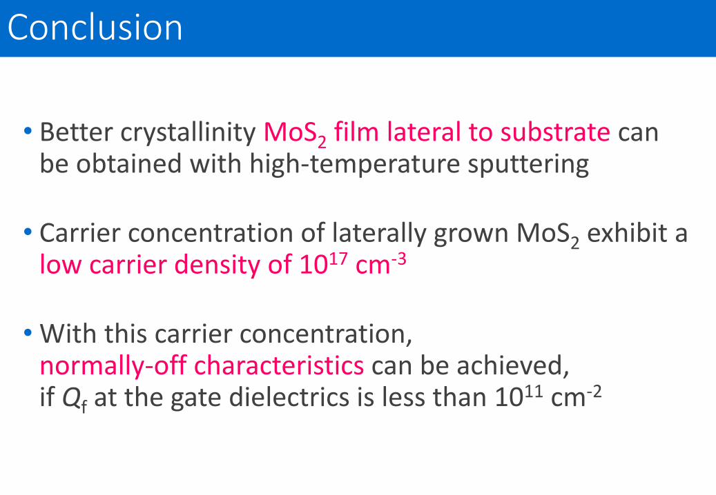
• Better crystallinity MoS2 film lateral to substrate can be obtained with high-temperature sputtering
• Carrier concentration of laterally grown MoS2 exhibit a low carrier density of 1017 cm-3
• With this carrier concentration, normally-off characteristics can be achieved, if Qf at the gate dielectrics is less than 1011 cm-2

以下、素材
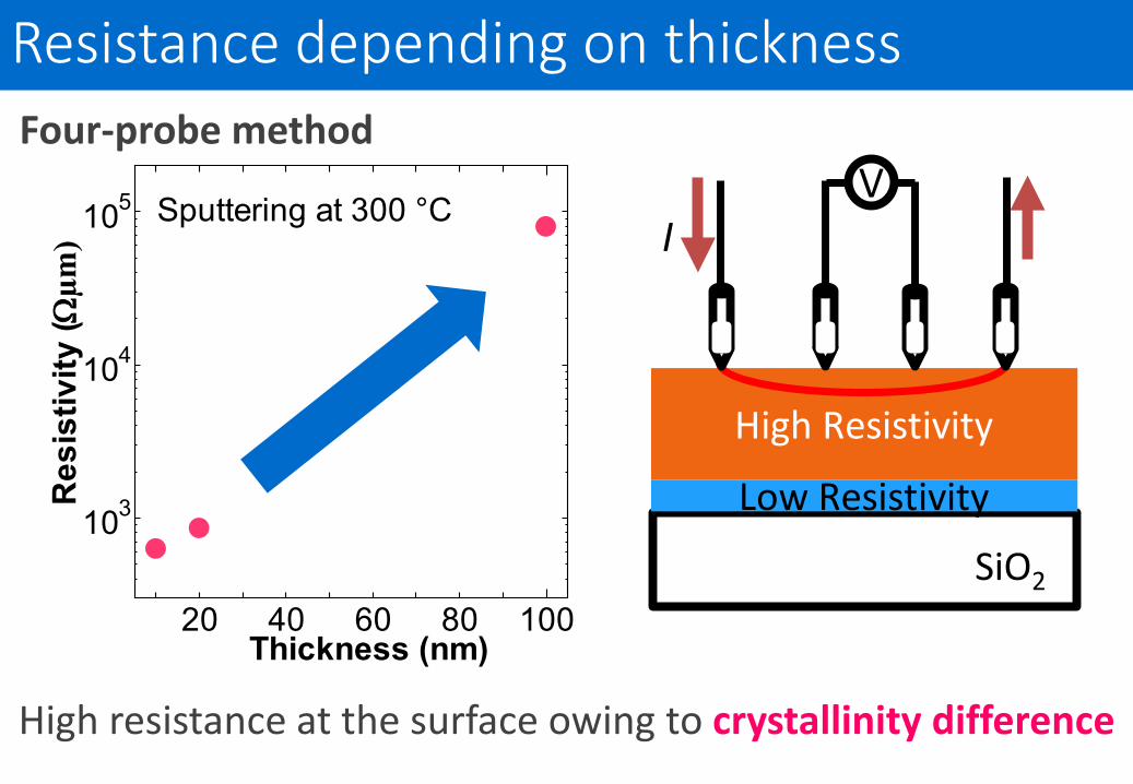
Resistance depending on thickness
SiO2
Low Resistivity
High Resistivity
VI
20 40 60 80 100
103
104
105
Thickness (nm)
Res
istiv
ity (Ω
µm)
Sputtering at 300 °C
High resistance at the surface owing to crystallinity difference
Four-probe method
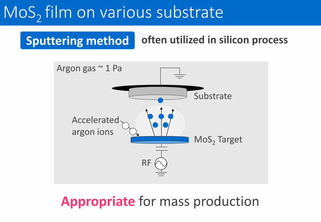
MoS2 film on various substrateoften utilized in silicon process
MoS2 Target
Substrate
RF
Acceleratedargon ions
Argon gas ~ 1 Pa
Sputtering method
Appropriate for mass production
以下、素材
0 10 20 301016
1017
1018
1019
1020
1021
Thickness (nm)
Car
rier D
ensi
ty (c
m−3
)
(high temp. sputtering)
B. Radisavljevic, et al, (2013).
This study
(exfoliation)
100
Decrease in carrier density (~ 10-3 times)
1 10 1000.0
0.5
1.0
1.5
2.0
2.5
Thickness (nm)
RM
S R
ough
ness
(nm
)Lateral layers
Perpendicularlayers
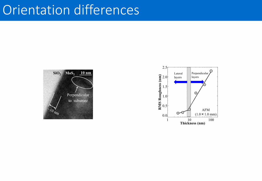
Orientation differences
10 nmSiO2 MoS2
Perpendicularto substrate
Laterallayers
Perpendicularlayers
1 10 1000.0
0.5
1.0
1.5
2.0
2.5
Thickness (nm)
RM
S R
ough
ness
(nm
)
AFM(1.0×1.0 mm)
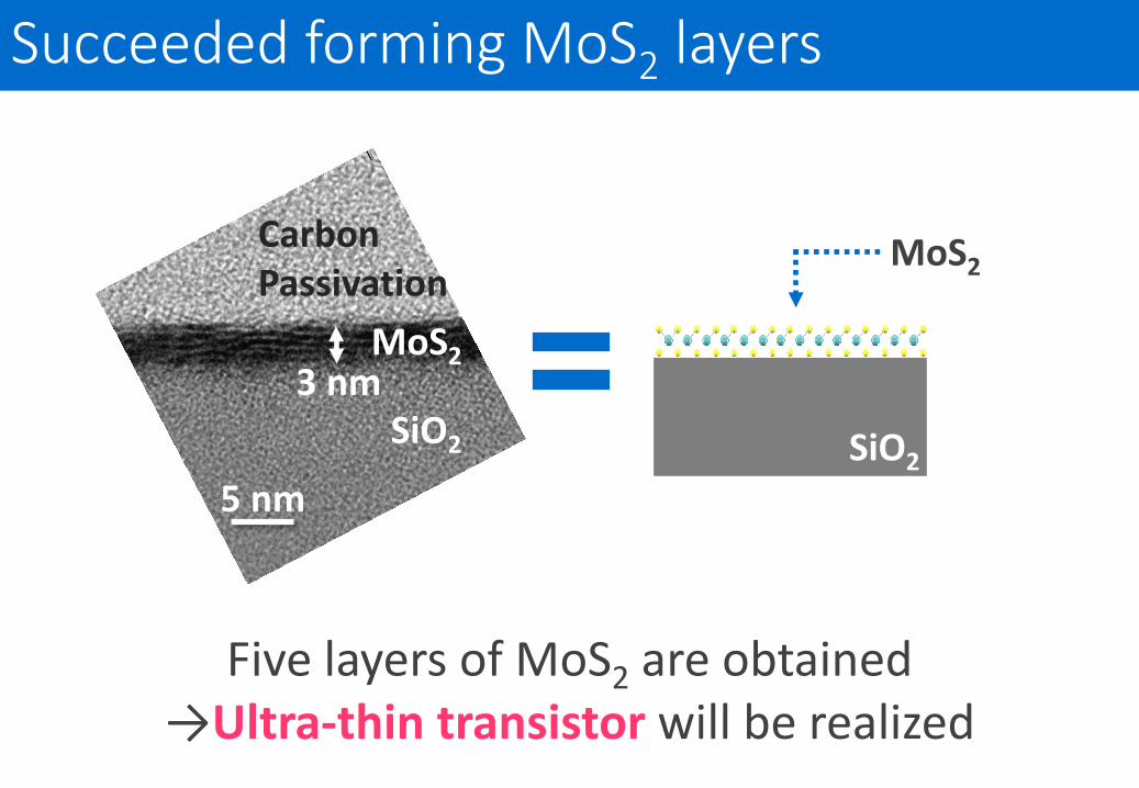
Succeeded forming MoS2 layers
3 nm
5 nm
SiO2
CarbonPassivation
MoS2
Five layers of MoS2 are obtained→Ultra-thin transistor will be realized
MoS2
SiO2
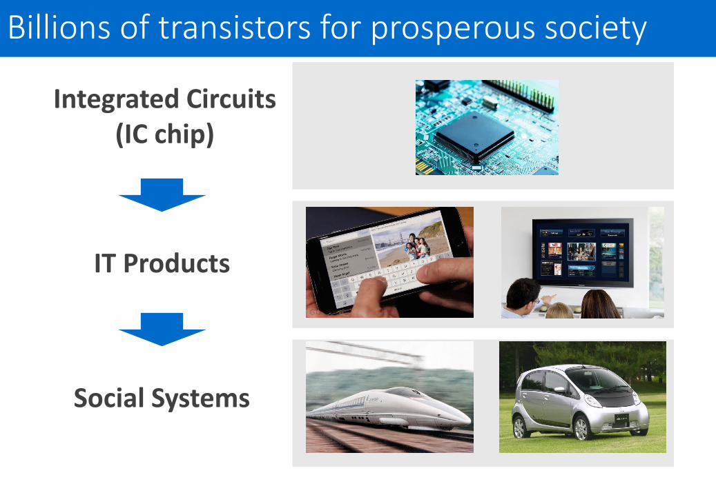
Billions of transistors for prosperous society
Integrated Circuits(IC chip)
IT Products
Social Systems
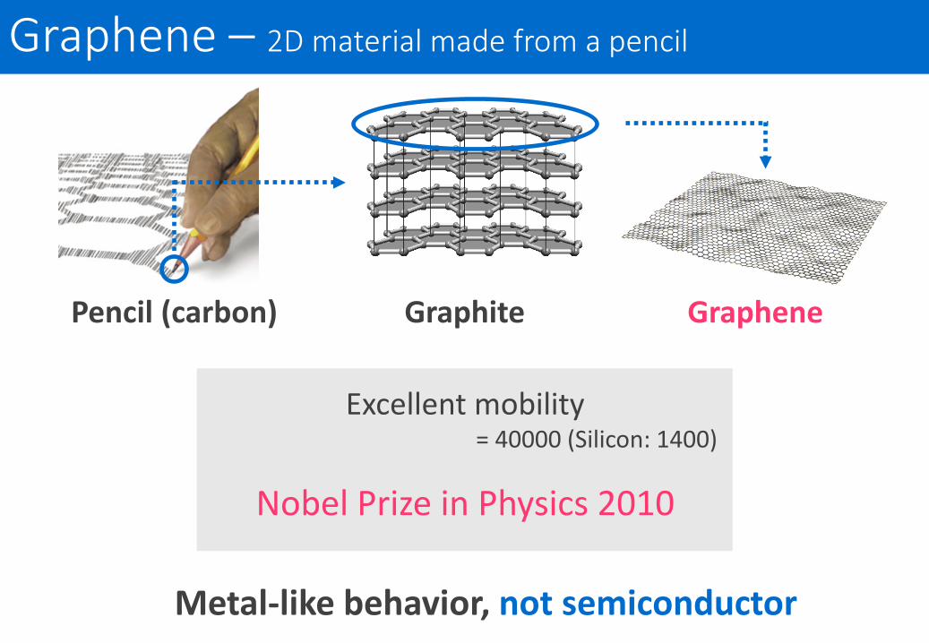
Graphene – 2D material made from a pencil
Excellent mobility
Pencil (carbon) Graphite Graphene
Metal-like behavior, not semiconductor
Nobel Prize in Physics 2010
= 40000 (Silicon: 1400)
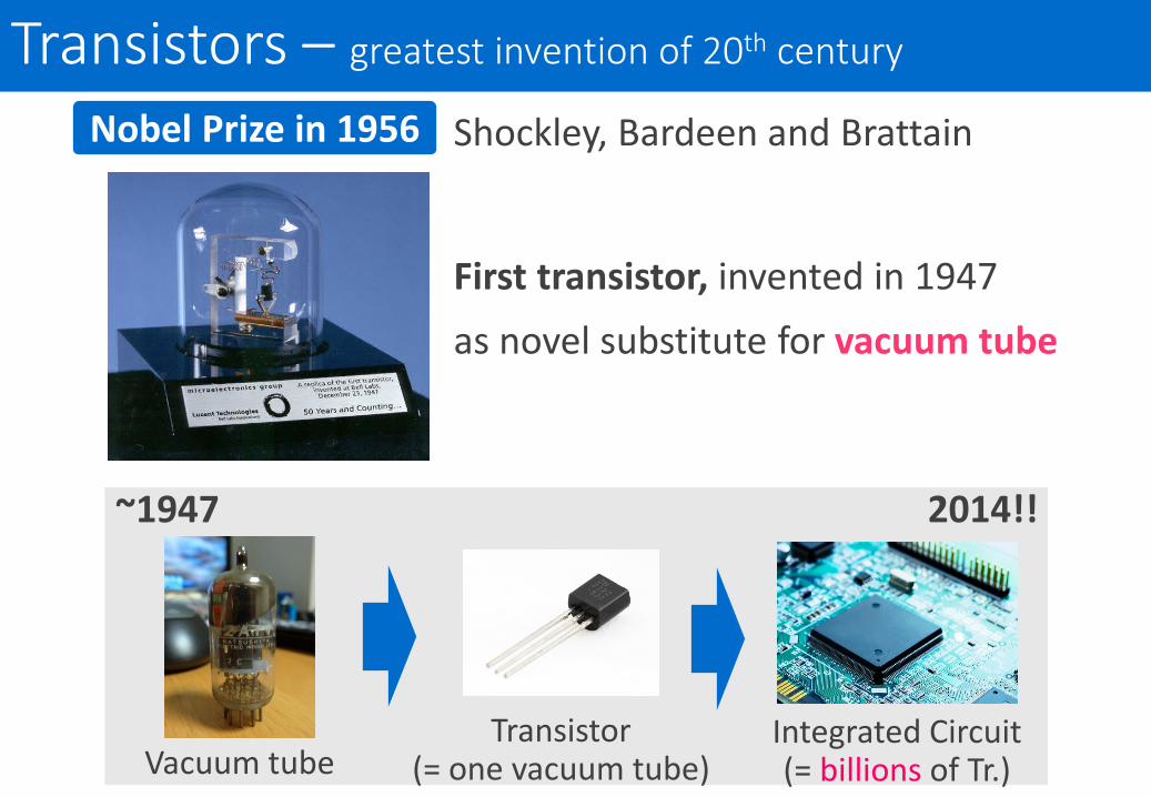
Transistors – greatest invention of 20th century
Nobel Prize in 1956 Shockley, Bardeen and Brattain
Vacuum tubeTransistor
(= one vacuum tube)Integrated Circuit(= billions of Tr.)
as novel substitute for vacuum tubeFirst transistor, invented in 1947
2014!!~1947
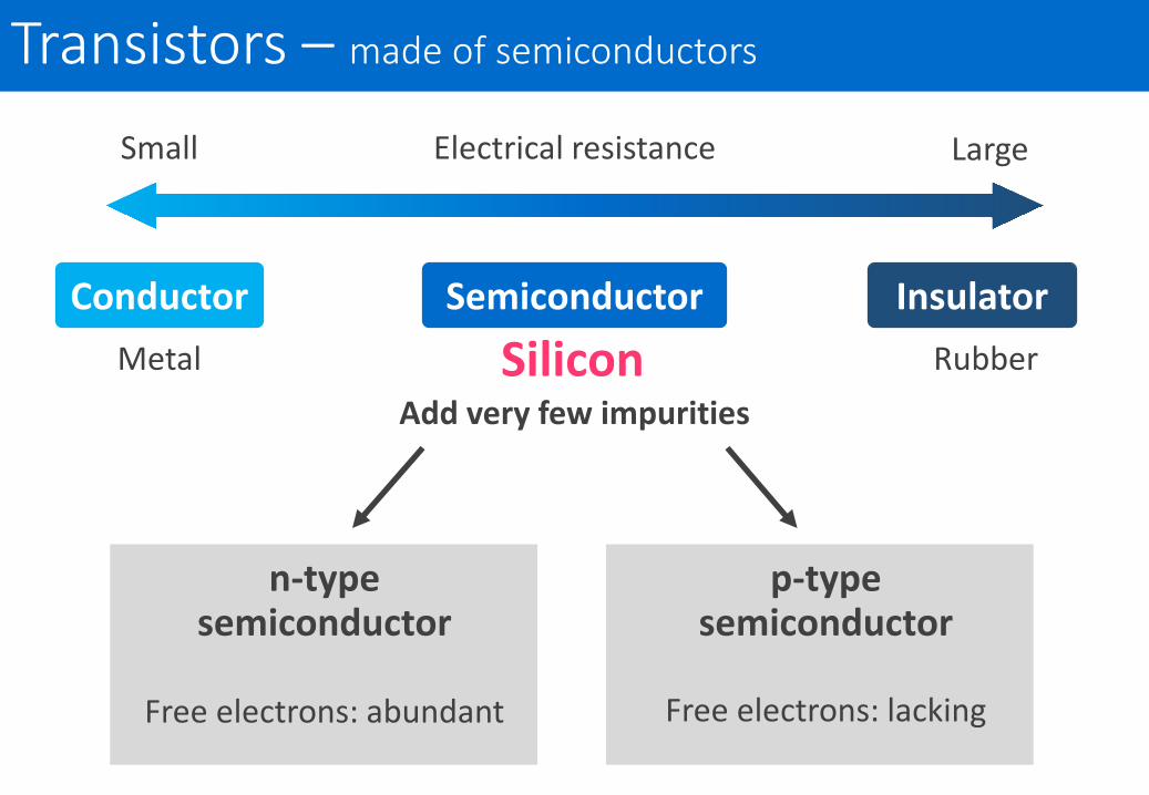
Transistors – made of semiconductors
Semiconductor
Electrical resistance LargeSmall
InsulatorConductorMetal RubberSilicon
n-typesemiconductor
p-typesemiconductor
Free electrons: abundant Free electrons: lacking
Add very few impurities
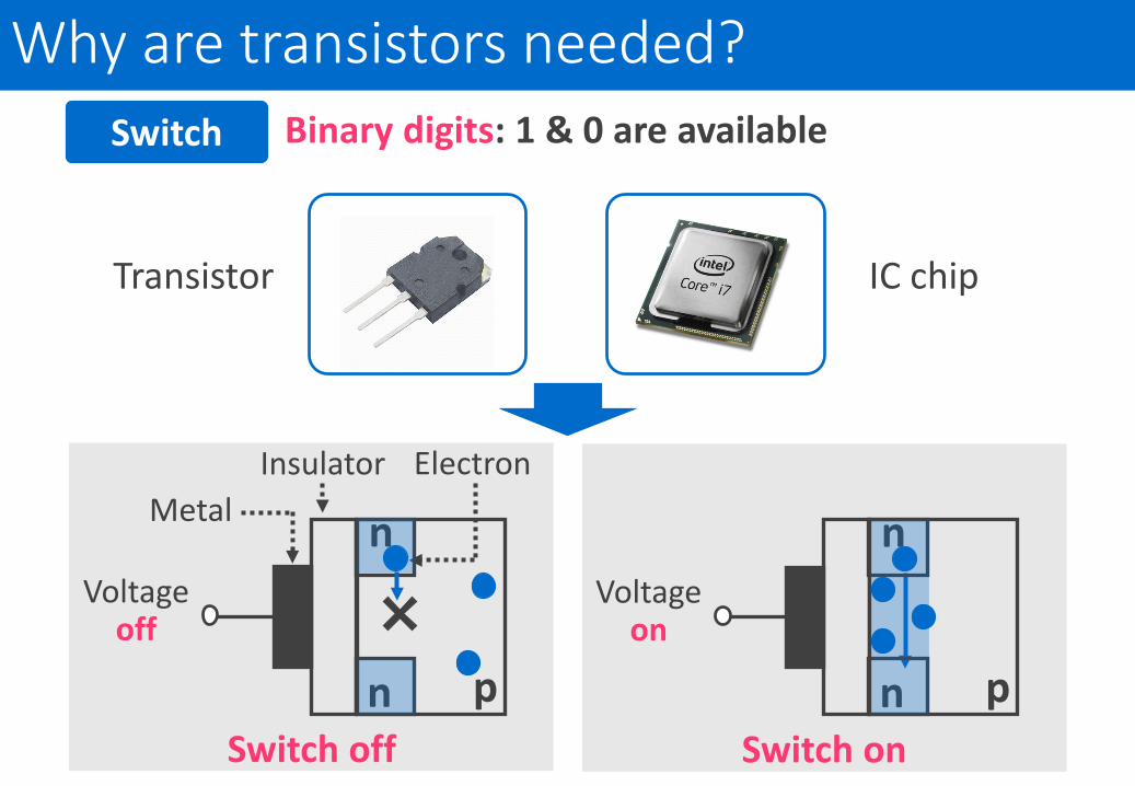
Why are transistors needed?
Transistor
Switch
InsulatorMetal n
n p
Voltageon
Electron
Switch on
n
n p
Voltageoff
Switch off
Binary digits: 1 & 0 are available
IC chip
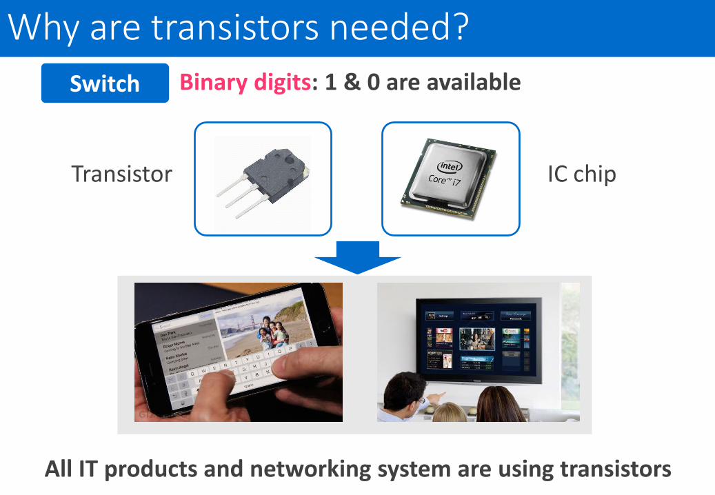
Why are transistors needed?
All IT products and networking system are using transistors
Switch Binary digits: 1 & 0 are available
Transistor IC chip
If there is no transistorsin the world…

More integration makes more prosperous society


![Broadband beamsplitter for high intensity laser ... · magnetron sputtering. The plant is also equipped with broadband monitoring (BBM) system [14] which was used in a passive mode](https://img.pdfslide.tips/doc/110x75/5e763a554d9da50d643ced87/broadband-beamsplitter-for-high-intensity-laser-magnetron-sputtering-the-plant.jpg)