Embed Size (px)
Citation preview
Multiscale approaches for electronic device simulation
M. Auf der Maur1, A. Pecchia2,
G. Penazzi3, A. Gagliardi4, F. Santoni1,
A. Di Carlo1
ECMI 2016
13-17 June 2016:
(1) University of Rome “Tor Vergata”
(2) CNR-ISMN, Italy
(3) BCCMS, University of Bremen
(4) TU Munich, Germany
University of Rome “Tor Vergata” - Dep. Electronic Engineering
EC
MI
2016
– S
an
tiag
o d
e C
om
po
ste
la,
13-1
7 J
un
e 2
016
2
Outline
• Why multiscale simulations?
• Multiscale coupling schemes, implementation concepts
• Atomistic/continuous coupling
• Examples
• Outlook
University of Rome “Tor Vergata” - Dep. Electronic Engineering
EC
MI
2016
– S
an
tiag
o d
e C
om
po
ste
la,
13-1
7 J
un
e 2
016
3
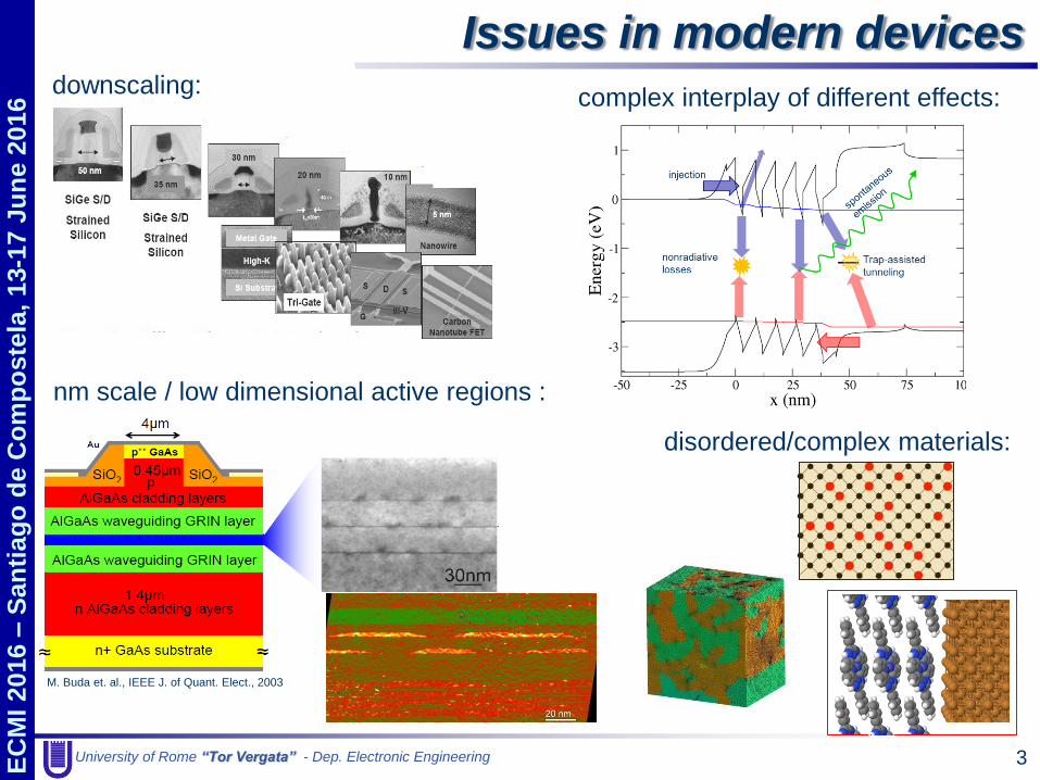
Issues in modern devices
M. Buda et. al., IEEE J. of Quant. Elect., 2003
downscaling:
nm scale / low dimensional active regions :
complex interplay of different effects:
disordered/complex materials:
University of Rome “Tor Vergata” - Dep. Electronic Engineering
EC
MI
2016
– S
an
tiag
o d
e C
om
po
ste
la,
13-1
7 J
un
e 2
016
4
Multiscale initiatives
• Increasing number of publications on multiscale
simulation of electronic devices
• Several international actions, in US and Europe:
– Specific calls
– Since 2012 a ERC bottom up counsil: EMMC
– Multiscale materials modeling cluster gathering FP7/H2020
projects
– COST action MultiscaleSolar
University of Rome “Tor Vergata” - Dep. Electronic Engineering
EC
MI
2016
– S
an
tiag
o d
e C
om
po
ste
la,
13-1
7 J
un
e 2
016
5
Atomistic/discrete + continuum
• Coupling atomistic or discrete models with continuum
models is of special interest:
– ultrascaled devices (few nm dimensions)
– CNTs, graphene, 2D materials
– alloy fluctuations (e.g. in InGaN, SiGe)
– SL, thin layers with sub-ML thickness (e.g. in AlInGaP
devices)
University of Rome “Tor Vergata” - Dep. Electronic Engineering
EC
MI
2016
– S
an
tiag
o d
e C
om
po
ste
la,
13-1
7 J
un
e 2
016
6
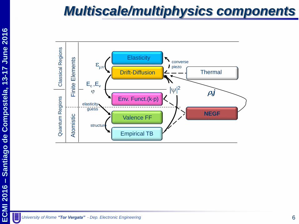
Multiscale/multiphysics components
Cla
ssic
al R
egio
ns
Elasticity
Drift-Diffusion Thermal
NEGF
Qu
an
tum
Re
gio
ns
Env. Funct.(k p)
Valence FF
Empirical TB Ato
mis
tic
Fin
ite
Ele
me
nts
Ec ,Ev
converse
piezo
structure
elasticity
guess
2 ,j
University of Rome “Tor Vergata” - Dep. Electronic Engineering
EC
MI
2016
– S
an
tiag
o d
e C
om
po
ste
la,
13-1
7 J
un
e 2
016
7
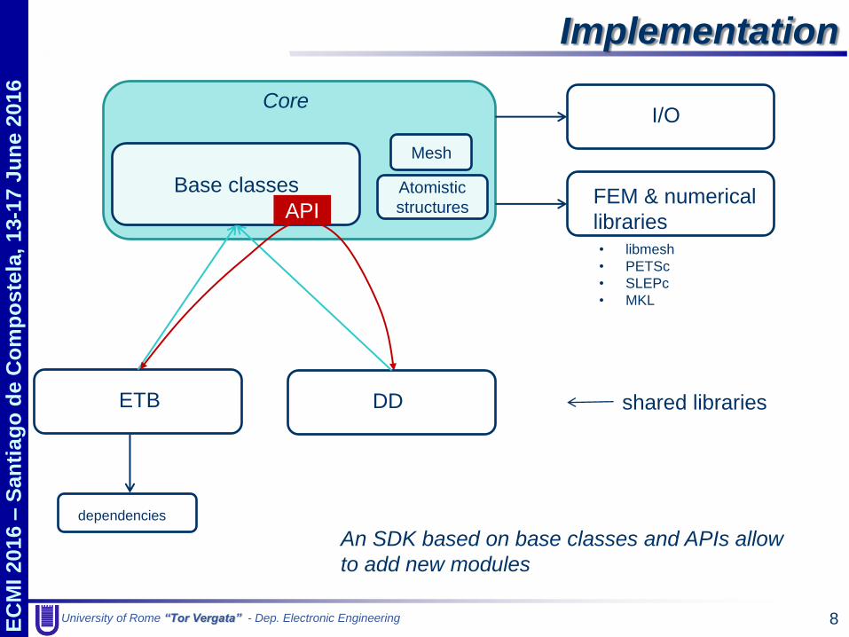
Implementation: TiberCAD
• Object oriented design
• Implementation is done in modular way, making use of
hierarchies of classes
• An API in the base classes provides functionality for
interchange of data between modules
• Continuous models are implemented using FEM
• Electronic transport: drift-diffusion, using electrochemical
potentials as variables
University of Rome “Tor Vergata” - Dep. Electronic Engineering
EC
MI
2016
– S
an
tiag
o d
e C
om
po
ste
la,
13-1
7 J
un
e 2
016
8
Implementation
Base classes
Core
FEM & numerical
libraries
I/O
ETB DD
dependencies
API
shared libraries
• libmesh
• PETSc
• SLEPc
• MKL
Mesh
Atomistic
structures
An SDK based on base classes and APIs allow
to add new modules
University of Rome “Tor Vergata” - Dep. Electronic Engineering
EC
MI
2016
– S
an
tiag
o d
e C
om
po
ste
la,
13-1
7 J
un
e 2
016
9
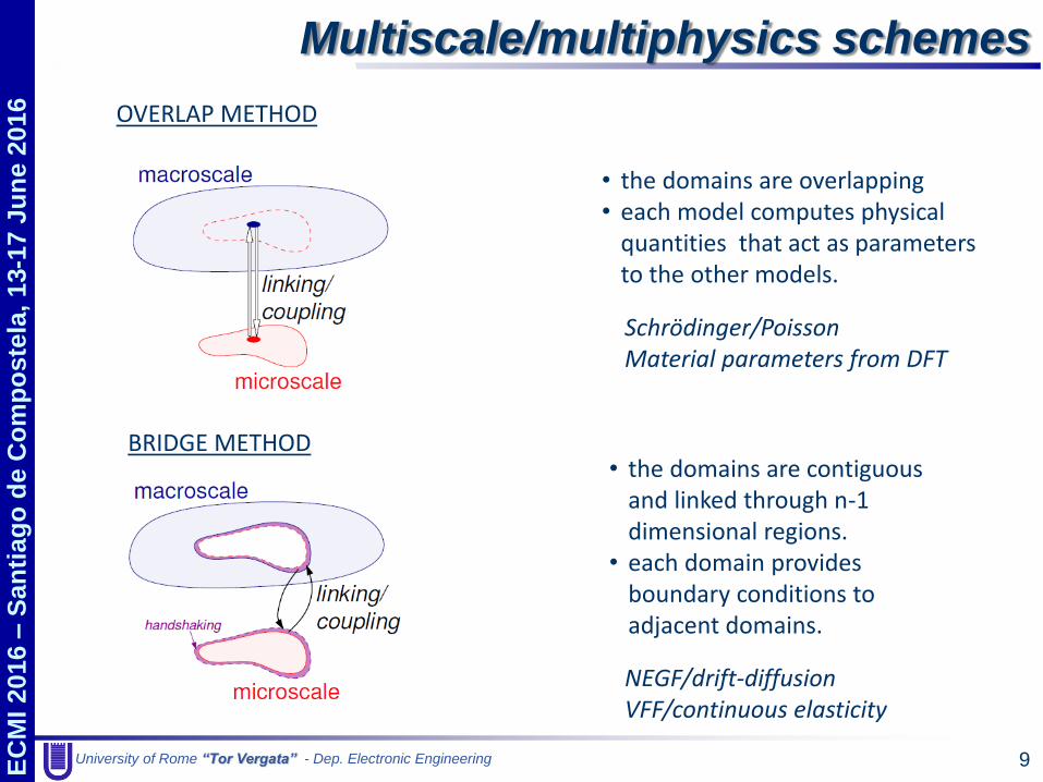
Multiscale/multiphysics schemes
BRIDGE METHOD • the domains are contiguous
and linked through n-1 dimensional regions.
• each domain provides boundary conditions to adjacent domains.
OVERLAP METHOD
• the domains are overlapping • each model computes physical
quantities that act as parameters to the other models.
Schrödinger/Poisson Material parameters from DFT
NEGF/drift-diffusion VFF/continuous elasticity
University of Rome “Tor Vergata” - Dep. Electronic Engineering
EC
MI
2016
– S
an
tiag
o d
e C
om
po
ste
la,
13-1
7 J
un
e 2
016
10
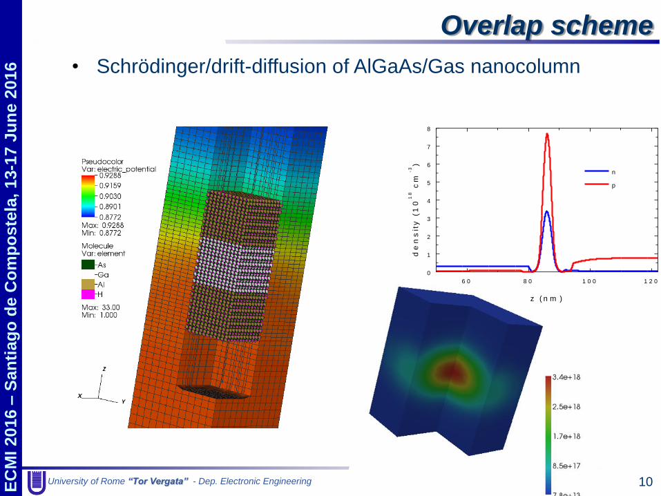
Overlap scheme
• Schrödinger/drift-diffusion of AlGaAs/Gas nanocolumn
6 0 8 0 1 0 0 1 2 0
0
1
2
3
4
5
6
7
8
n
p
de
ns
ity
(1
01
8
cm
-3
)
z ( n m )
University of Rome “Tor Vergata” - Dep. Electronic Engineering
EC
MI
2016
– S
an
tiag
o d
e C
om
po
ste
la,
13-1
7 J
un
e 2
016
11
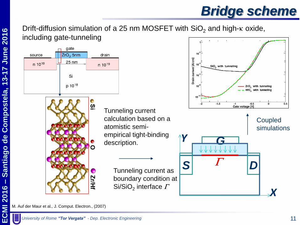
Bridge scheme Drift-diffusion simulation of a 25 nm MOSFET with SiO2 and high- oxide,
including gate-tunneling
Tunneling current
calculation based on a
atomistic semi-
empirical tight-binding
description.
M. Auf der Maur et al., J. Comput. Electron., (2007)
Coupled
simulations
Tunneling current as
boundary condition at
Si/SiO2 interface
G
D S
X
Y
University of Rome “Tor Vergata” - Dep. Electronic Engineering
EC
MI
2016
– S
an
tiag
o d
e C
om
po
ste
la,
13-1
7 J
un
e 2
016
12
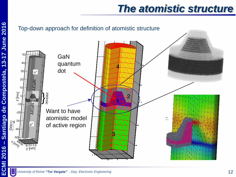
The atomistic structure
GaN
quantum
dot
Want to have
atomistic model
of active region
Top-down approach for definition of atomistic structure
University of Rome “Tor Vergata” - Dep. Electronic Engineering
EC
MI
2016
– S
an
tiag
o d
e C
om
po
ste
la,
13-1
7 J
un
e 2
016
13
Atomistic structure generation
• We can assure a consistent atomistic structure using a top
down approach:
1. Identify relevant volume
2. Fill up with atoms using the
crystal basis
3. Cut / fold atoms outside of
the structure
It is important that all atoms
are lying inside the
simulation domain
• The approach works for pseudomorphic structures with
commensurate interfaces
• Structure is strained to the reference material
• Every atom is associated to a mesh element
• Can produce random alloys (uniform and non-uniform)
University of Rome “Tor Vergata” - Dep. Electronic Engineering
EC
MI
2016
– S
an
tiag
o d
e C
om
po
ste
la,
13-1
7 J
un
e 2
016
14
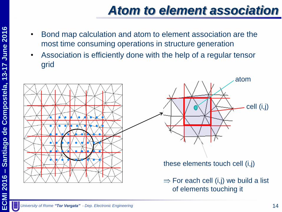
Atom to element association
• Bond map calculation and atom to element association are the
most time consuming operations in structure generation
• Association is efficiently done with the help of a regular tensor
grid
atom
cell (i,j)
these elements touch cell (i,j)
For each cell (i,j) we build a list
of elements touching it
University of Rome “Tor Vergata” - Dep. Electronic Engineering
EC
MI
2016
– S
an
tiag
o d
e C
om
po
ste
la,
13-1
7 J
un
e 2
016
15
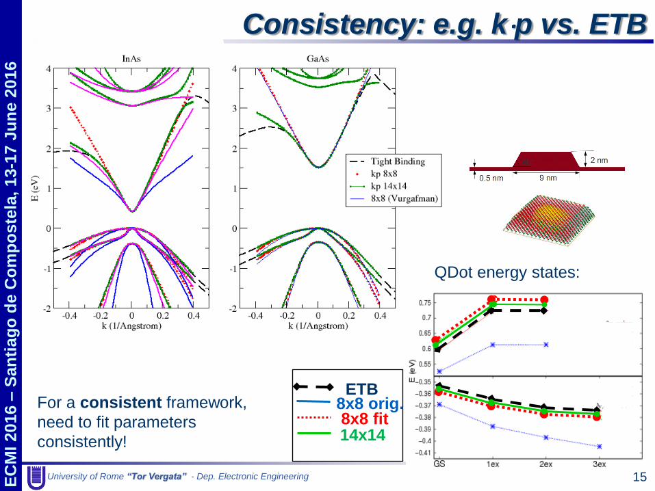
Consistency: e.g. k p vs. ETB
ETB 8x8 orig. 8x8 fit 14x14
For a consistent framework,
need to fit parameters
consistently!
QDot energy states:
University of Rome “Tor Vergata” - Dep. Electronic Engineering
EC
MI
2016
– S
an
tiag
o d
e C
om
po
ste
la,
13-1
7 J
un
e 2
016
16
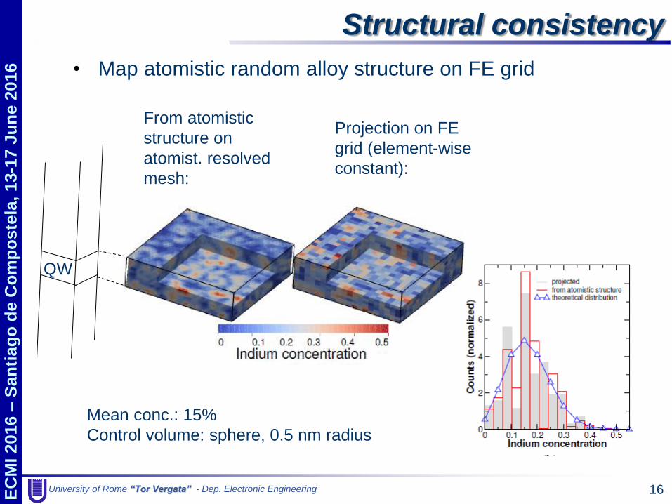
Structural consistency
• Map atomistic random alloy structure on FE grid
QW
From atomistic
structure on
atomist. resolved
mesh:
Projection on FE
grid (element-wise
constant):
Mean conc.: 15%
Control volume: sphere, 0.5 nm radius
University of Rome “Tor Vergata” - Dep. Electronic Engineering
EC
MI
2016
– S
an
tiag
o d
e C
om
po
ste
la,
13-1
7 J
un
e 2
016
17
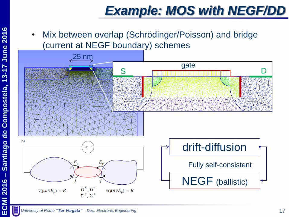
Example: MOS with NEGF/DD
S D
drift-diffusion
NEGF (ballistic)
Fully self-consistent
25 nm
• Mix between overlap (Schrödinger/Poisson) and bridge
(current at NEGF boundary) schemes
gate
University of Rome “Tor Vergata” - Dep. Electronic Engineering
EC
MI
2016
– S
an
tiag
o d
e C
om
po
ste
la,
13-1
7 J
un
e 2
016
18
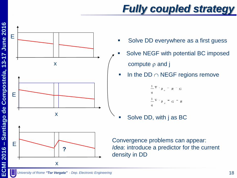
In the DD NEGF regions remove
Solve DD, with j as BC
Fully coupled strategy
Solve DD everywhere as a first guess
RG
q
GR
q
p
n
J
J
1
1
E
x
E
x
E
x
?
Convergence problems can appear:
Idea: introduce a predictor for the current
density in DD
Solve NEGF with potential BC imposed
compute and j
University of Rome “Tor Vergata” - Dep. Electronic Engineering
EC
MI
2016
– S
an
tiag
o d
e C
om
po
ste
la,
13-1
7 J
un
e 2
016
19
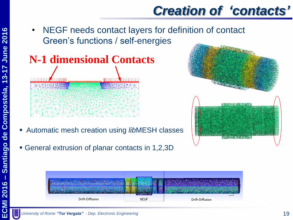
Creation of „contacts‟
N-1 dimensional Contacts
Automatic mesh creation using libMESH classes
General extrusion of planar contacts in 1,2,3D
• NEGF needs contact layers for definition of contact
Green’s functions / self-energies
University of Rome “Tor Vergata” - Dep. Electronic Engineering
EC
MI
2016
– S
an
tiag
o d
e C
om
po
ste
la,
13-1
7 J
un
e 2
016
20
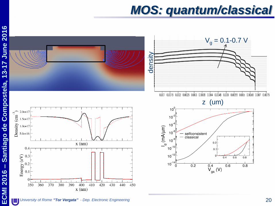
MOS: quantum/classical
z (um)
density
Vg = 0.1-0.7 V
z (um)
University of Rome “Tor Vergata” - Dep. Electronic Engineering
EC
MI
2016
– S
an
tiag
o d
e C
om
po
ste
la,
13-1
7 J
un
e 2
016
21
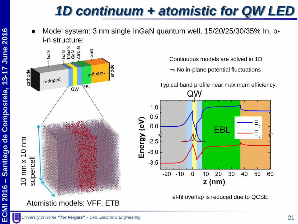
1D continuum + atomistic for QW LED
Continuous models are solved in 1D
No in-plane potential fluctuations
10 n
m x
10 n
m
superc
ell
Model system: 3 nm single InGaN quantum well, 15/20/25/30/35% In, p-
i-n structure:
Atomistic models: VFF, ETB
Typical band profile near maximum efficiency:
el-hl overlap is reduced due to QCSE
University of Rome “Tor Vergata” - Dep. Electronic Engineering
EC
MI
2016
– S
an
tiag
o d
e C
om
po
ste
la,
13-1
7 J
un
e 2
016
22
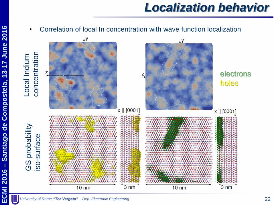
Localization behavior
• Correlation of local In concentration with wave function localization
holes
electrons
Lo
ca
l In
diu
m
co
nce
ntr
atio
n
GS
pro
ba
bili
ty
iso
-su
rfa
ce
University of Rome “Tor Vergata” - Dep. Electronic Engineering
EC
MI
2016
– S
an
tiag
o d
e C
om
po
ste
la,
13-1
7 J
un
e 2
016
23
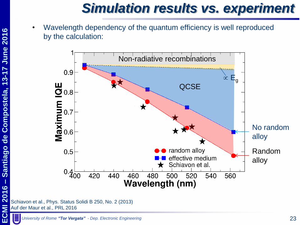
Simulation results vs. experiment
• Wavelength dependency of the quantum efficiency is well reproduced
by the calculation:
Schiavon et al., Phys. Status Solidi B 250, No. 2 (2013)
Auf der Maur et al., PRL 2016
Non-radiative recombinations
Eg
QCSE
No random
alloy
Random
alloy
University of Rome “Tor Vergata” - Dep. Electronic Engineering
EC
MI
2016
– S
an
tiag
o d
e C
om
po
ste
la,
13-1
7 J
un
e 2
016
24
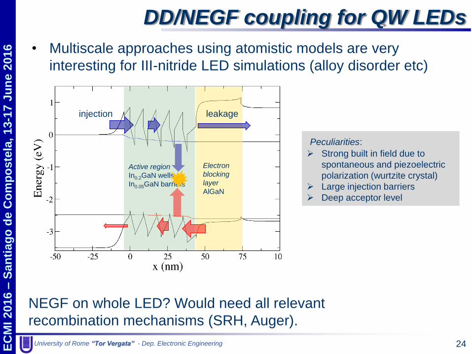
DD/NEGF coupling for QW LEDs
• Multiscale approaches using atomistic models are very
interesting for III-nitride LED simulations (alloy disorder etc)
Peculiarities:
Strong built in field due to
spontaneous and piezoelectric
polarization (wurtzite crystal)
Large injection barriers
Deep acceptor level
injection leakage
Electron
blocking
layer
AlGaN
Active region
In0.2GaN wells
In0.05GaN barriers
NEGF on whole LED? Would need all relevant
recombination mechanisms (SRH, Auger).
University of Rome “Tor Vergata” - Dep. Electronic Engineering
EC
MI
2016
– S
an
tiag
o d
e C
om
po
ste
la,
13-1
7 J
un
e 2
016
25
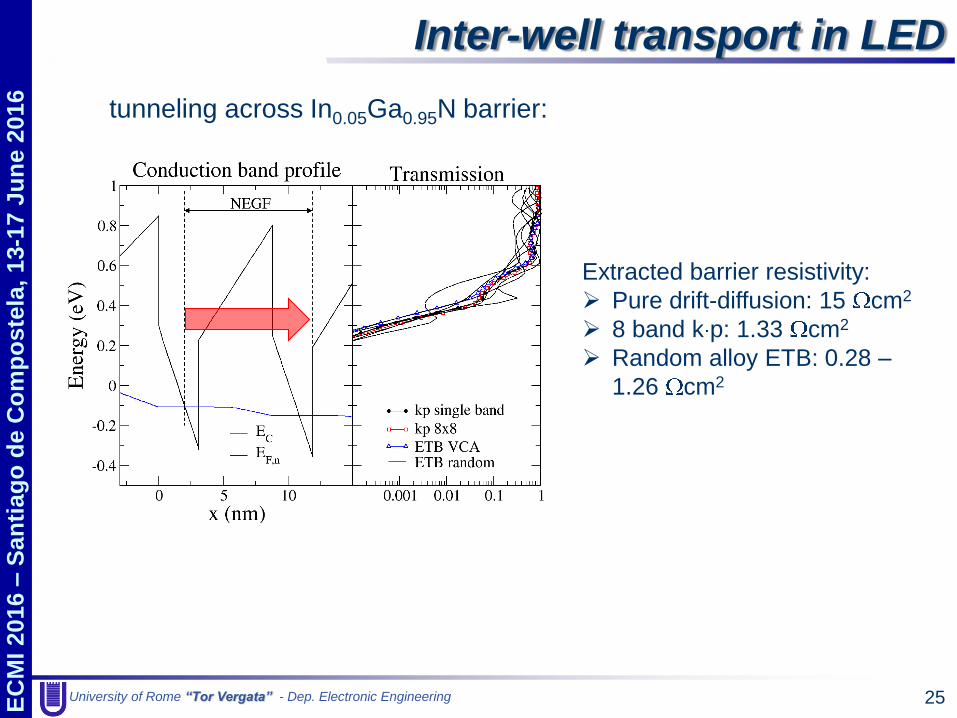
Inter-well transport in LED
tunneling across In0.05Ga0.95N barrier:
Extracted barrier resistivity:
Pure drift-diffusion: 15 cm2
8 band k p: 1.33 cm2
Random alloy ETB: 0.28 –
1.26 cm2
University of Rome “Tor Vergata” - Dep. Electronic Engineering
EC
MI
2016
– S
an
tiag
o d
e C
om
po
ste
la,
13-1
7 J
un
e 2
016
26
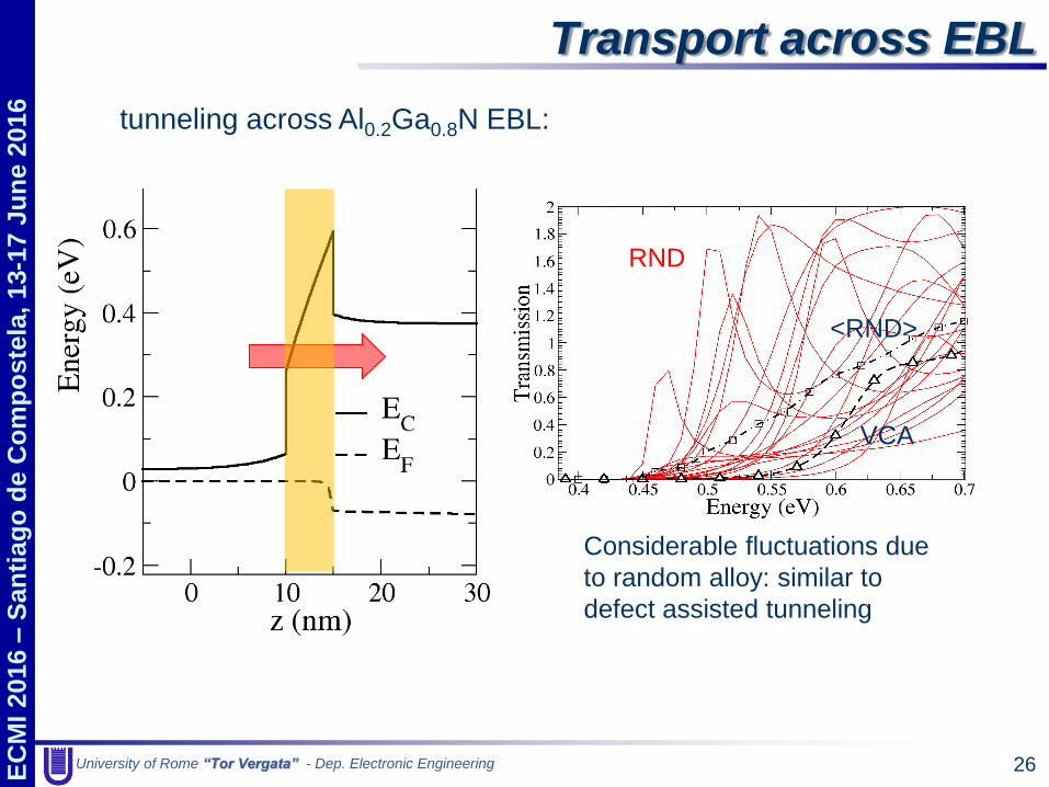
Transport across EBL
tunneling across Al0.2Ga0.8N EBL:
Considerable fluctuations due
to random alloy: similar to
defect assisted tunneling
RND
<RND>
VCA
University of Rome “Tor Vergata” - Dep. Electronic Engineering
EC
MI
2016
– S
an
tiag
o d
e C
om
po
ste
la,
13-1
7 J
un
e 2
016
27
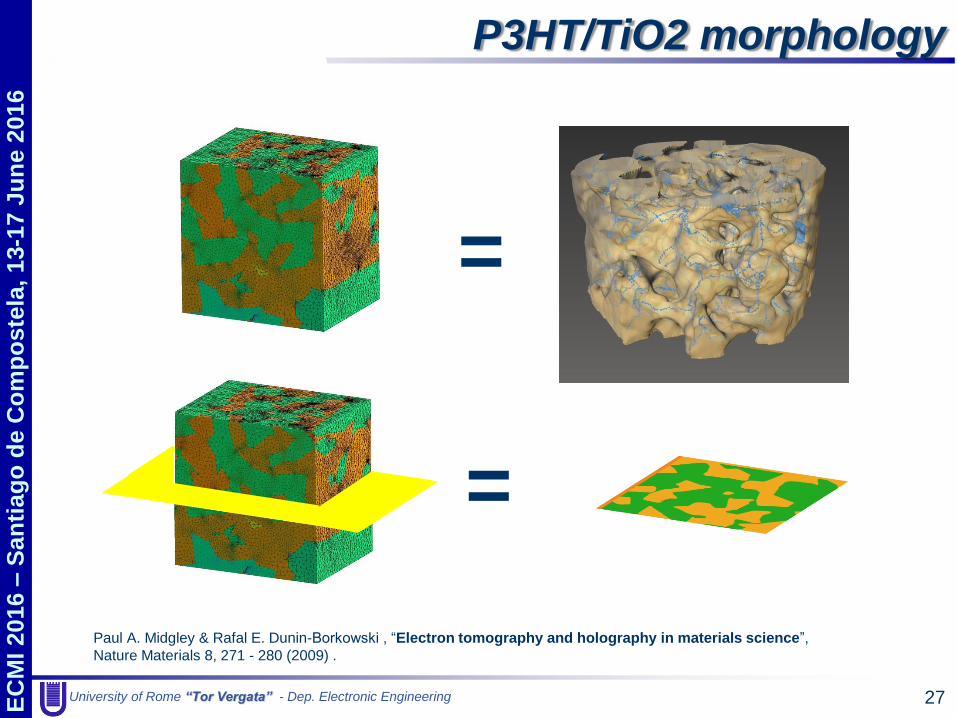
P3HT/TiO2 morphology
=
=
Paul A. Midgley & Rafal E. Dunin-Borkowski , “Electron tomography and holography in materials science”,
Nature Materials 8, 271 - 280 (2009) .
University of Rome “Tor Vergata” - Dep. Electronic Engineering
EC
MI
2016
– S
an
tiag
o d
e C
om
po
ste
la,
13-1
7 J
un
e 2
016
28
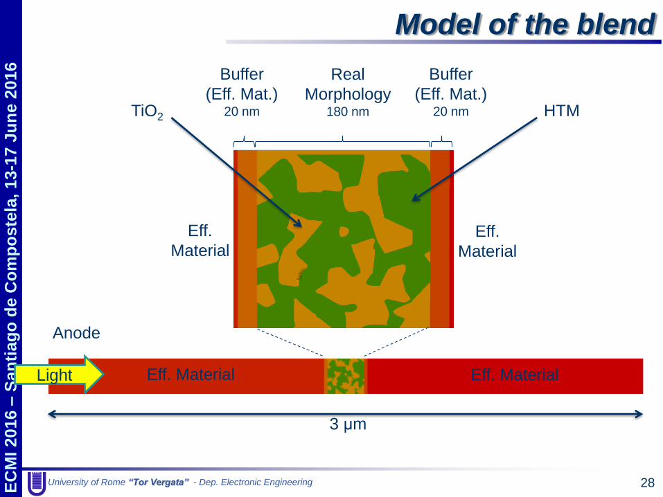
Model of the blend
3 μm
Anode
Eff. Material Eff. Material
Eff.
Material Eff.
Material
Buffer
(Eff. Mat.) 20 nm
Real
Morphology 180 nm
Buffer
(Eff. Mat.) 20 nm
Light
TiO2 HTM
University of Rome “Tor Vergata” - Dep. Electronic Engineering
EC
MI
2016
– S
an
tiag
o d
e C
om
po
ste
la,
13-1
7 J
un
e 2
016
29
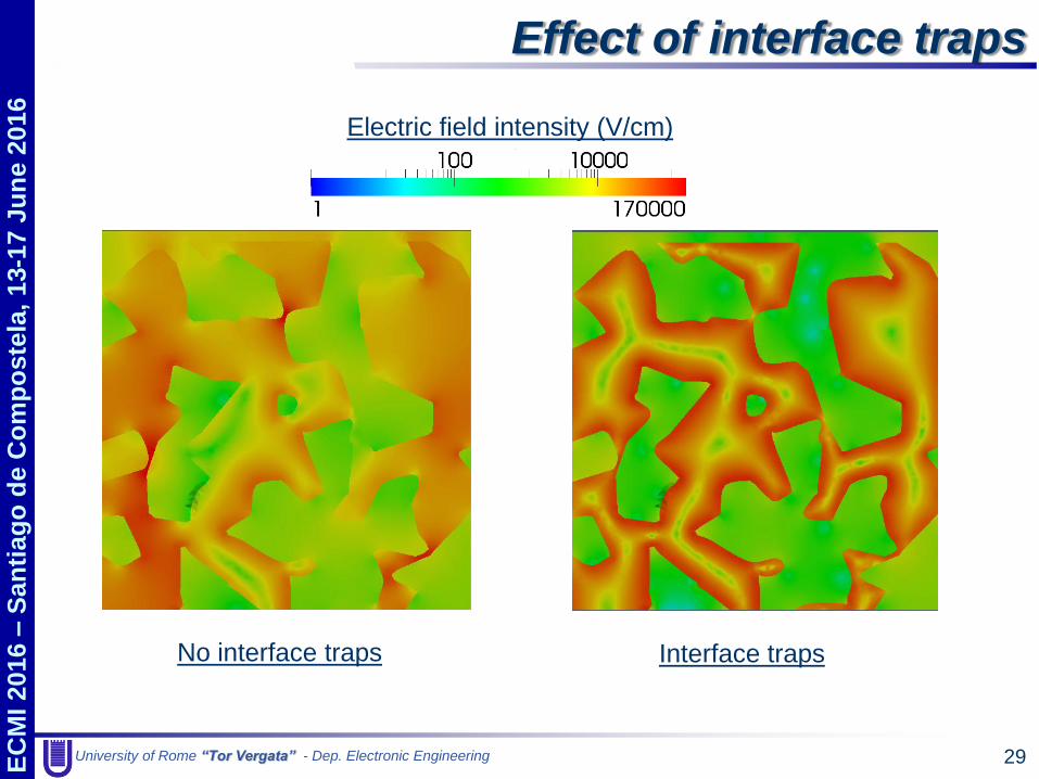
Effect of interface traps
No interface traps Interface traps
Electric field intensity (V/cm)
University of Rome “Tor Vergata” - Dep. Electronic Engineering
EC
MI
2016
– S
an
tiag
o d
e C
om
po
ste
la,
13-1
7 J
un
e 2
016
30
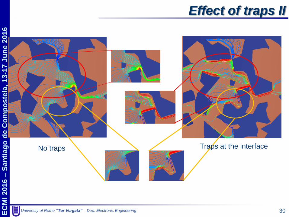
Effect of traps II
No traps Traps at the interface
University of Rome “Tor Vergata” - Dep. Electronic Engineering
EC
MI
2016
– S
an
tiag
o d
e C
om
po
ste
la,
13-1
7 J
un
e 2
016
31
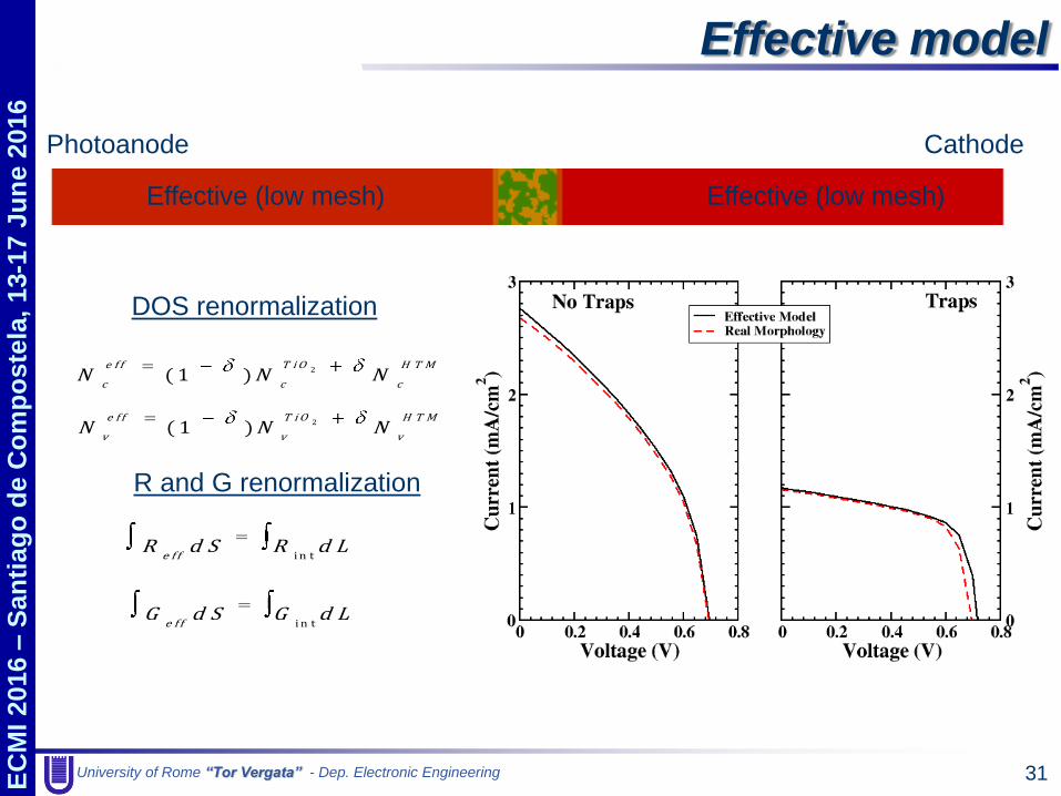
Effective model
Effective (low mesh) Effective (low mesh)
Photoanode Cathode
i n te f fR d S R d L
i n te f fG d S G d L
2( 1 )e f f T i O H T M
c c cN N N
2( 1 )e f f T i O H T M
v v vN N N
DOS renormalization
R and G renormalization
University of Rome “Tor Vergata” - Dep. Electronic Engineering
EC
MI
2016
– S
an
tiag
o d
e C
om
po
ste
la,
13-1
7 J
un
e 2
016
32
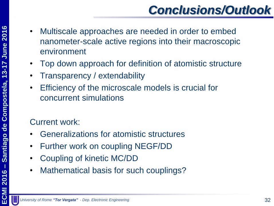
Conclusions/Outlook
• Multiscale approaches are needed in order to embed
nanometer-scale active regions into their macroscopic
environment
• Top down approach for definition of atomistic structure
• Transparency / extendability
• Efficiency of the microscale models is crucial for
concurrent simulations
Current work:
• Generalizations for atomistic structures
• Further work on coupling NEGF/DD
• Coupling of kinetic MC/DD
• Mathematical basis for such couplings?
University of Rome “Tor Vergata” - Dep. Electronic Engineering
EC
MI
2016
– S
an
tiag
o d
e C
om
po
ste
la,
13-1
7 J
un
e 2
016
33
Acknowledgements
Thank you
Prof. Aldo Di Carlo
Dr. A. Pecchia
Dr. F. Sacconi
Dr. G. Penazzi
Dr. G. Romano
Dr. A. Gagliardi
Dr. M. Lopez
Dr. D. Barettin
Dr. D. Gentilini
Dr. F. Santoni
Dr. W. Rodrigues
D. Rossi
Multiscale Device Simulator
http://www.tibercad.org FP7-ICT NEWLED
No. FP7-318388
H2020-NMP2014/2015
No. 646259


![[DL輪読会]Parallel Multiscale Autoregressive Density Estimation](https://img.pdfslide.tips/doc/110x75/5a64d62f7f8b9a88148b589b/dlparallel-multiscale-autoregressive-density-estimation.jpg)