Embed Size (px)
Citation preview
Multiscale beam evolution and shapingin corrugated plasmonic systems
S. Thongrattanasiri,2 D. C. Adams,1 D. Wasserman,1
and V. A. Podolskiy1,∗1 Department of Physics and Applied Physics, University of Massachusetts Lowell, 136 Olney
Hall, One University Ave, Lowell, Massachusetts 01854, USA2 Department of Physics, Oregon State University, 301 Weniger Hall, Corvallis, Oregon
97331, USA∗viktor [email protected]
Abstract: We analyze, theoretically and experimentally, the dynamicsof the wavepackets in plasmonic beaming devices, and show that the beamevolution in this class of structures is a multiscale phenomenon, whichinitiates in the near-field proximity of the device, develops continuouslyover a new length scale many times the wavelength of the light, and iscompleted well into the far-field of the system. We develop a quantitativedescription of the light evolution in the beaming structures and verify ourtheoretical predictions with experiments. Our analytical results are utilizedto develop plasmonic geometries for shaping the mid-field beam evolution,and experimental results from these structures are demonstrated.
© 2011 Optical Society of America
OCIS codes: (240.6680) Surface plasmons; (260.3160) Interference; (260.3060) Infrared.
References and links1. J. D. Joannopoulos, R. D. Meade, and J. N. Winn, Photonic Crystals: Molding the flow of light (Princeton U.
Press, 1995).2. D. R. Smith, W. J. Padilla, D. C. Vier, S. C. Nemat-Nasser, and S. Schultz, “Composite medium with simultane-
ously negative permeability and permittivity,” Phys. Rev. Lett. 84, 4184–4187 (2000).3. U. Leonhardt, “Optical conformal mapping,” Science 312, 1777–1780 (2006).4. W. Cai, U. K. Chettiar, A. V. Kildishev, and V. M. Shalaev, “Optical cloaking with metamaterials,” Nature Photon.
1, 224–227 (2007).5. H. J. Lezec, A. Degiron, E. Devaux, R. A. Linke, L. Martın-Moreno, F. J. Garcıa-Vidal, and T. W. Ebbesen,
“Beaming light from a subwavelength aperture,” Science 297, 820–822 (2002).6. L. Martın-Moreno, F. J. Garcıa-Vidal, H. J. Lezec, A. Degiron, and T. W. Ebbesen, “Theory of highly directional
emission from a single subwavelength aperture surrounded by surface corrugations,” Phys. Rev. Lett. 90, 167401(2003).
7. F. J. Garcıa-Vidal, L. Martın-Moreno, H. J. Lezec, and T. W. Ebbesen, “Focusing light with a single subwave-length aperture flanked by surface corrugations,” Appl. Phys. Lett. 83, 4500–4502 (2003).
8. D. C. Adams, S. Thongrattanasiri, T. Ribaudo, V. A. Podolskiy, and D. Wasserman, “Plasmonic mid-infraredbeam steering,” Appl. Phys. Lett. 96, 201112 (2010).
9. N. Yu, J. Fan, Q. J. Wang, C. Pflugl, L. Diehl, T. Edamura, M. Yamanishi, H. Kan, and F. Capasso, “Small-divergence semiconductor lasers by plasmonic collimation,” Nature Photon. 2, 564–570 (2008).
10. M. Born and E. Wolf, Principles of Optics (Cambridge Univ., 1999).11. H. Raether, Surface Plasmons on Smooth and Rough Surfaces and on Gratings (Springer-Verlag, 1988).12. S. I. Bozhevolnyi, V. S. Volkov, E. Devaux, J.-Y. Laluet, and T. W. Ebbesen, “Channel plasmon subwavelength
waveguide components including interferometers and ring resonators,” Nature 440, 508–511 (2006).13. W. L. Barnes, A. Dereux, and T. W. Ebbesen, “Surface plasmon subwavelength optics,” Nature 424, 824–830
(2003).14. A. Krier, Mid-infrared Semiconductor Optoelectronics (Springer, 2006).
#142612 - $15.00 USD Received 15 Feb 2011; revised 11 Apr 2011; accepted 16 Apr 2011; published 27 Apr 2011(C) 2011 OSA 9 May 2011 / Vol. 19, No. 10 / OPTICS EXPRESS 9269
15. I. I. Smolyaninov, D. L. Mazzoni, and C. D. Davis, “Imaging of surface plasmon scattering by lithographicallycreated individual surface defects,” Phys. Rev. Lett. 77, 3877–3880 (2003).
16. I. I. Smolyaninov, D. L. Mazzoni, J. Mait, and T. W. Ebbesen, “Experimental study of surface-plasmon scatteringby individual surface defects,” Phys. Rev. B 56, 1601–1611 (2003).
17. A. V. Shchegrov, I. V. Novikov, and A. A. Maradudin, “Scattering of surface plasmon polaritons by a circularlysymmetric surface defect,” Phys. Rev. Lett. 78, 4269–4272 (2003).
18. E.D. Palik, The Handbook of Optical Constants of Solids (Academic, 1997).19. M. A. Ordal, L. L. Long, R. J. Bell, R. R. Bell, R. W., Alexander Jr., and C. A. Ward, “Optical properties of
the metals Al, Co, Cu, Au, Fe, Pb, Ni, Pd, Pt, Ag, Ti, and W in the infrared and far infrared,” Appl. Optics 22,1099–1119 (1983).
20. For details see COMSOL Multiphysics 3.5a User’s Guide and RF Module User’s Guide, www.comsol.com.21. S. Thongrattanasiri, J. Elser, and V. A. Podolskiy, “Quasi-planar optics: computing light propagation and scatte-
ring in planar waveguide arrays,” J. Opt. Soc. Am. B 26, B102–B110 (2009).22. M. I. Amanti, M. Fischer, G. Scalari, M. Beck, and J. Faist, “Low-divergence single-mode terahertz quantum
cascade lase,” Nature Photon. 3, 586–590 (2009)
1. Introduction
Recent advances in fabrication, theory, and computational techniques have enabled a large classof composite materials [1–4] where light molding is an implicitly multiscale process. Here weconsider the problem of beaming in plasmonic structures whose extreme far-field propertieshave been described in [5–9], which link the far-field beam pattern to near-field propagation andscattering of excited surface waves. We show, experimentally and theoretically, that while beamformation in these unique devices initiates in the near-field, the beam develops continuouslyover a length scale many times the wavelength of the light (through the device “mid” field), andis completed well into the far-field of the system. This work allows for a new understandingof complex beam formation over this new lengthscale, opening the door to the integration ofbeam -steering and -shaping structures with miniaturized optical circuits, on-chip photonics,and lithographic and imaging systems.
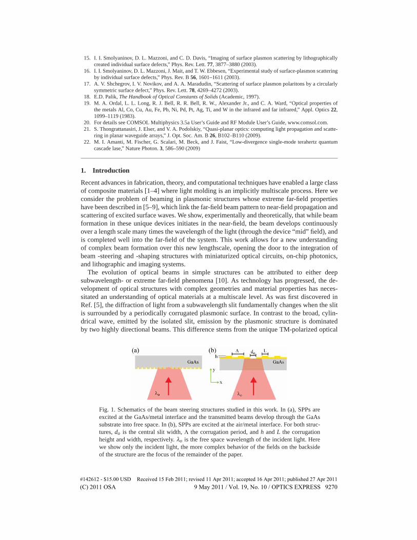
The evolution of optical beams in simple structures can be attributed to either deepsubwavelength- or extreme far-field phenomena [10]. As technology has progressed, the de-velopment of optical structures with complex geometries and material properties has neces-sitated an understanding of optical materials at a multiscale level. As was first discovered inRef. [5], the diffraction of light from a subwavelength slit fundamentally changes when the slitis surrounded by a periodically corrugated plasmonic surface. In contrast to the broad, cylin-drical wave, emitted by the isolated slit, emission by the plasmonic structure is dominatedby two highly directional beams. This difference stems from the unique TM-polarized optical
Fig. 1. Schematics of the beam steering structures studied in this work. In (a), SPPs areexcited at the GaAs/metal interface and the transmitted beams develop through the GaAssubstrate into free space. In (b), SPPs are excited at the air/metal interface. For both struc-tures, do is the central slit width, Λ the corrugation period, and h and L the corrugationheight and width, respectively. λo is the free space wavelength of the incident light. Herewe show only the incident light, the more complex behavior of the fields on the backsideof the structure are the focus of the remainder of the paper.
#142612 - $15.00 USD Received 15 Feb 2011; revised 11 Apr 2011; accepted 16 Apr 2011; published 27 Apr 2011(C) 2011 OSA 9 May 2011 / Vol. 19, No. 10 / OPTICS EXPRESS 9270
mode, guided by the interface between the dielectric and plasmonic media, known as a surfaceplasmon polariton (SPP) [11]. SPPs, often used for compact optical and opto-electronic struc-tures [12–14], can be coupled to conventional, free-space optics by surface inhomogeneities.This scattering of SPPs from surface defects was experimentally demonstrated and theoreti-cally described in earlier work demonstrating scattering from surface defects at short wave-lengths [15–17]. Schematics of the plasmonic beam steering devices fabricated on GaAs sub-strates, and characterized in this work, are shown in Fig. 1. In a typical beam steering devicesuch as the ones depicted in Fig. 1, SPPs, excited by a subwavelength aperture, propagate awayfrom the slit along the metal-dielectric interface. The periodic surface corrugation results in par-tial out-coupling of SPPs into free-space. As result, the light emitted by the device representsthe interference of the cylindrical wave emitted by the central hole and the portion of the origi-nal SPP scattered by the periodic surface corrugations [5–8]. Since the emission of the centralhole lacks directionality, the direction of the beams is determined solely by the interference ofSPP-scattered waves.
The direction corresponding to the interference maximum is given by the condition that, atthis ‘beaming’ angle, the phase of the light scattered by two neighboring surface corrugationsdiffers by 2π [6]:
k0 sinθ = kSPP − (2π −δ )/Λ, (1)
where k0 and kSPP correspond to the wavevector of the propagating waves above the gratingand that of the SPP, respectively, and the parameter δ describes the retardation of the phaseof the SPP caused by an individual corrugation (see below). This relationship describes the ex-treme far-field response of the system, and is typically measured experimentally, with a detectorpositioned at a centimeter- (or larger) distance from the sample, well into the far-field of theplasmonic structure.
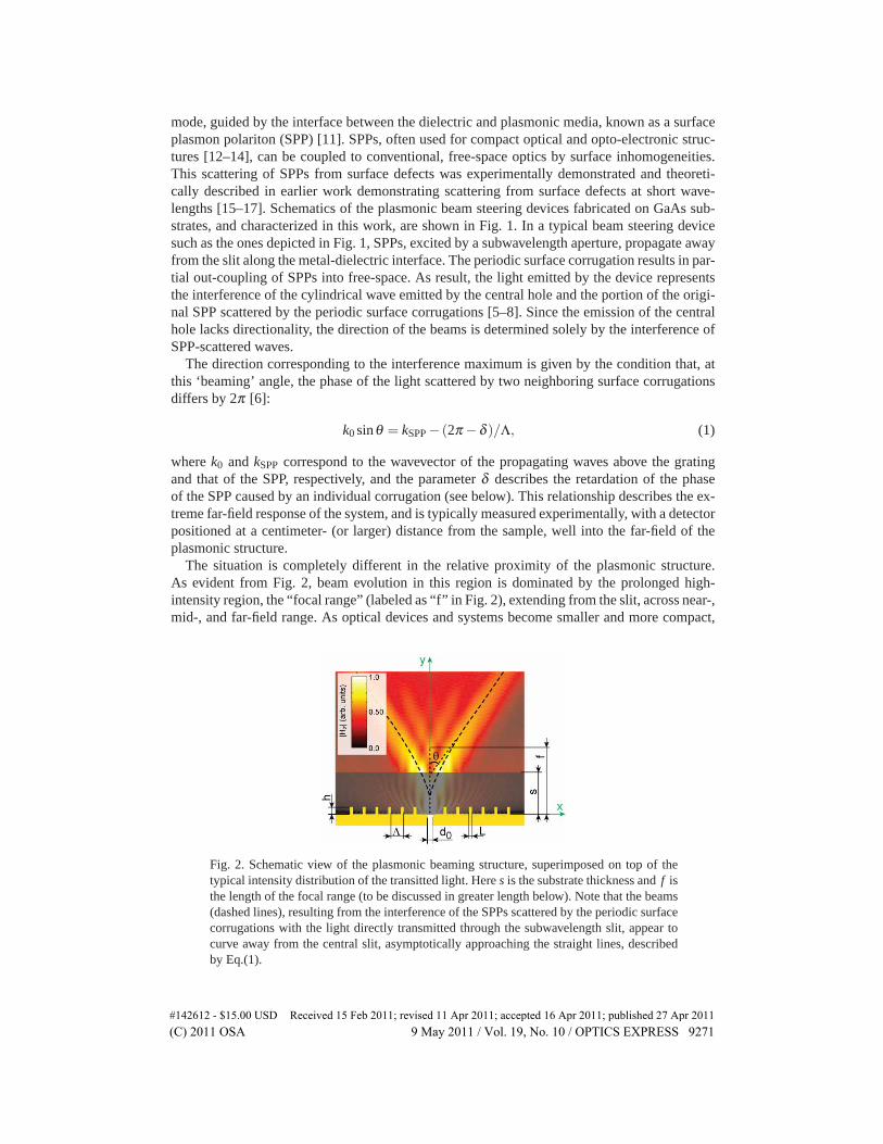
The situation is completely different in the relative proximity of the plasmonic structure.As evident from Fig. 2, beam evolution in this region is dominated by the prolonged high-intensity region, the “focal range” (labeled as “f” in Fig. 2), extending from the slit, across near-,mid-, and far-field range. As optical devices and systems become smaller and more compact,
Fig. 2. Schematic view of the plasmonic beaming structure, superimposed on top of thetypical intensity distribution of the transitted light. Here s is the substrate thickness and f isthe length of the focal range (to be discussed in greater length below). Note that the beams(dashed lines), resulting from the interference of the SPPs scattered by the periodic surfacecorrugations with the light directly transmitted through the subwavelength slit, appear tocurve away from the central slit, asymptotically approaching the straight lines, describedby Eq.(1).
#142612 - $15.00 USD Received 15 Feb 2011; revised 11 Apr 2011; accepted 16 Apr 2011; published 27 Apr 2011(C) 2011 OSA 9 May 2011 / Vol. 19, No. 10 / OPTICS EXPRESS 9271
understanding the evolution of light on the scale of 1 to 100 wavelengths becomes criticalfor the correct design and development of these systems. This motivates the necessity to gaininsight into the origin of the focal range formation in the beamsteering devices.
In this manuscript we provide the comprehensive analysis of this exciting phenomenon. Themanuscript is structured as follows: Section 2 presents our main analytical results, describesthe numerical approach for their validation, and summarizes the numerical studies. Section 3describes the experimental data supporting the phenomenon of the focal range formation. InSection 4, we use the developed formalism to design and realize plasmonic-grating mid-fieldfocusing structures. Section 5 concludes the paper.
2. Analytical Results and their Numerical Verification
2.1. SPP transmission and scattering from corrugations
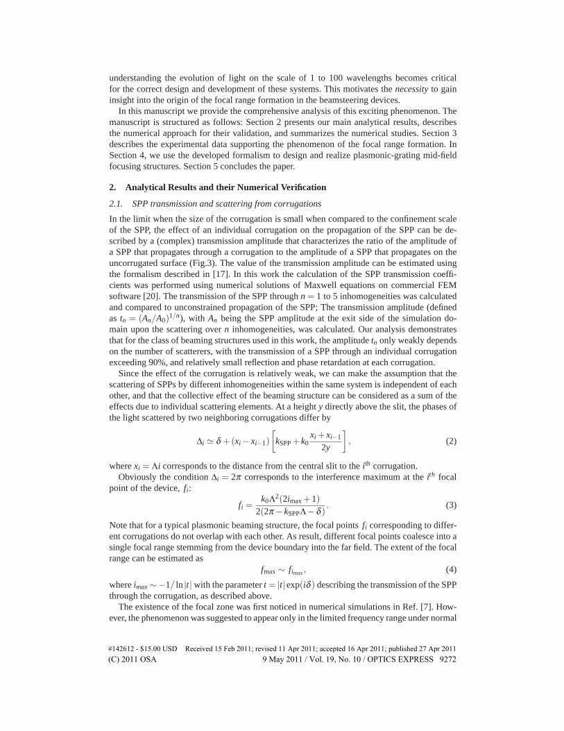
In the limit when the size of the corrugation is small when compared to the confinement scaleof the SPP, the effect of an individual corrugation on the propagation of the SPP can be de-scribed by a (complex) transmission amplitude that characterizes the ratio of the amplitude ofa SPP that propagates through a corrugation to the amplitude of a SPP that propagates on theuncorrugated surface (Fig.3). The value of the transmission amplitude can be estimated usingthe formalism described in [17]. In this work the calculation of the SPP transmission coeffi-cients was performed using numerical solutions of Maxwell equations on commercial FEMsoftware [20]. The transmission of the SPP through n = 1 to 5 inhomogeneities was calculatedand compared to unconstrained propagation of the SPP; The transmission amplitude (definedas tn = (An/A0)
1/n), with An being the SPP amplitude at the exit side of the simulation do-main upon the scattering over n inhomogeneities, was calculated. Our analysis demonstratesthat for the class of beaming structures used in this work, the amplitude tn only weakly dependson the number of scatterers, with the transmission of a SPP through an individual corrugationexceeding 90%, and relatively small reflection and phase retardation at each corrugation.
Since the effect of the corrugation is relatively weak, we can make the assumption that thescattering of SPPs by different inhomogeneities within the same system is independent of eachother, and that the collective effect of the beaming structure can be considered as a sum of theeffects due to individual scattering elements. At a height y directly above the slit, the phases ofthe light scattered by two neighboring corrugations differ by
Δi � δ +(xi − xi−1)
[kSPP + k0
xi + xi−1
2y
], (2)
where xi = Λi corresponds to the distance from the central slit to the ith corrugation.Obviously the condition Δi = 2π corresponds to the interference maximum at the ith focal
point of the device, fi:
fi =k0Λ2(2imax +1)
2(2π − kSPPΛ−δ ). (3)
Note that for a typical plasmonic beaming structure, the focal points fi corresponding to differ-ent corrugations do not overlap with each other. As result, different focal points coalesce into asingle focal range stemming from the device boundary into the far field. The extent of the focalrange can be estimated as
fmax ∼ fimax , (4)
where imax ∼−1/ ln |t| with the parameter t = |t|exp(iδ ) describing the transmission of the SPPthrough the corrugation, as described above.
The existence of the focal zone was first noticed in numerical simulations in Ref. [7]. How-ever, the phenomenon was suggested to appear only in the limited frequency range under normal
#142612 - $15.00 USD Received 15 Feb 2011; revised 11 Apr 2011; accepted 16 Apr 2011; published 27 Apr 2011(C) 2011 OSA 9 May 2011 / Vol. 19, No. 10 / OPTICS EXPRESS 9272
beaming conditions (θ � 0). One of the main results of this work is the demonstration (bothanalytically and experimentally) of the fact that light focusing is a universal phenomenon, ap-pearing in the majority of plasmonic gratings and other grating-outcoupled waveguides [9,22].
In all these structures, the end of the focal region corresponds to the transition between thefew-corrugation interference (dominating the near- to mid-field zone of the device) and thecollective interference dominating the extreme far-field behavior. In particular, this transitionresults in the formation of the beams, which are seen to be originating in the proximity to fmax.For shorter wavelengths fi < 0, indicating that the focal spot is “virtual”, so that the beamsappear to be emanating from behind the corrugated surface.
As pointed out above, the beams themselves are the result of constructive interference oflight scattered by the corrugated plasmonic surface. However, depending on the geometry of thedevice [11], this light can be in- or out-of-phase with the light emitted by the central slit. Thephase relation between the slit- and surface-originated beams determines whether the beamsappear at maxima or minima in the far-field response.
In the mid-field, however, the phase difference between the light emitted from the central slitand the light scattered by corrugations strongly depends on the coordinate y. Thus, the focalrange always manifests itself as set of interference maxima.
2.2. Calculation of field distribution in the system
In order to gain insight into the wave propagation in multiscale plasmonic structures and toverify the validity of the analytical equations describing the far- (Eq. 1) and mid- (Eq. 3) fieldbeam profiles we calculate the intensity distribution in the plasmonic beaming structures vianumerical solutions of Maxwell equations. Two alternative techniques have been used to cal-culate the field distribution in the system. First, the beam evolution has been calculated viacommercially-available finite-element-method (FEM) PDE solver [20]. The simulation spacein our models was at least 300μm-long and at least 450μm-high. The maximum size of the
Fig. 3. (a) Depiction of an individual scattering event of a SPP propagating across the smallbump on the otherwise smooth plasmonic surface. As result of this scattering, a (small) por-tion of the SPP energy is converted into free-space radiation, seen as the beam propagatingupward (dashed white curves). The amplitude of the SPP whose field profile is schemat-ically shown as the red shaded region is reduced, and its phase is (slightly) advanced.(b)Transmission and phase shift of SPP propagating through dielectric inserts. Note thatmore than 90 % of the SPP’s energy transfers through the insert. The phase of SPP isslightly advanced during the process. The 5 sets of solid (transmission) and dotted (phaseshift) lines correspond to transmission though 1 to 5 inserts, t1 . . .t5; the lines of differentcolor almost overlap, indicating that multiple-scattering can be omitted.
#142612 - $15.00 USD Received 15 Feb 2011; revised 11 Apr 2011; accepted 16 Apr 2011; published 27 Apr 2011(C) 2011 OSA 9 May 2011 / Vol. 19, No. 10 / OPTICS EXPRESS 9273
wavelength, µm6 7 8 9 10 11 12
-500
0
500
1000
f max
, µm
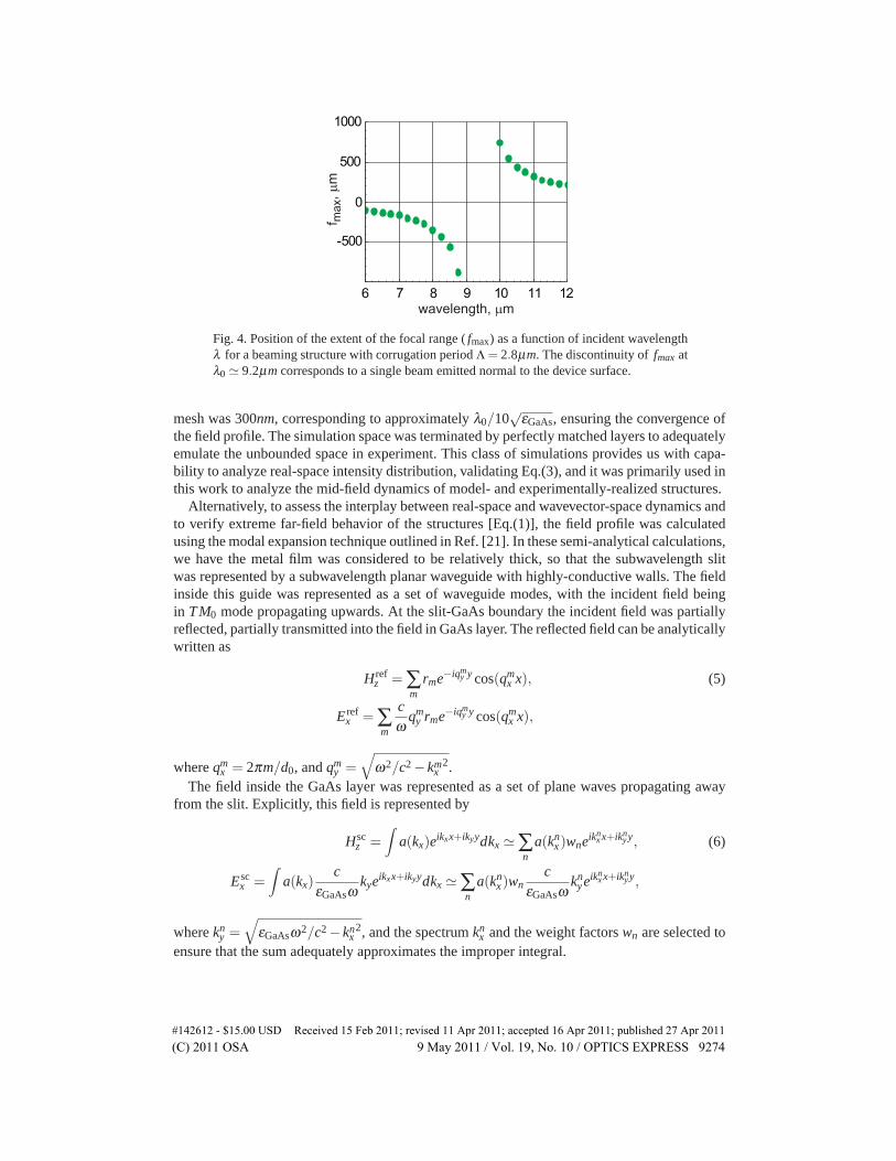
Fig. 4. Position of the extent of the focal range ( fmax) as a function of incident wavelengthλ for a beaming structure with corrugation period Λ = 2.8μm. The discontinuity of fmax atλ0 � 9.2μm corresponds to a single beam emitted normal to the device surface.
mesh was 300nm, corresponding to approximately λ0/10√
εGaAs, ensuring the convergence ofthe field profile. The simulation space was terminated by perfectly matched layers to adequatelyemulate the unbounded space in experiment. This class of simulations provides us with capa-bility to analyze real-space intensity distribution, validating Eq.(3), and it was primarily used inthis work to analyze the mid-field dynamics of model- and experimentally-realized structures.
Alternatively, to assess the interplay between real-space and wavevector-space dynamics andto verify extreme far-field behavior of the structures [Eq.(1)], the field profile was calculatedusing the modal expansion technique outlined in Ref. [21]. In these semi-analytical calculations,we have the metal film was considered to be relatively thick, so that the subwavelength slitwas represented by a subwavelength planar waveguide with highly-conductive walls. The fieldinside this guide was represented as a set of waveguide modes, with the incident field beingin TM0 mode propagating upwards. At the slit-GaAs boundary the incident field was partiallyreflected, partially transmitted into the field in GaAs layer. The reflected field can be analyticallywritten as
Hrefz = ∑
mrme−iqm
y y cos(qmx x), (5)
Erefx = ∑
m
cω
qmy rme−iqm
y y cos(qmx x),
where qmx = 2πm/d0, and qm
y =√
ω2/c2 − kmx
2.The field inside the GaAs layer was represented as a set of plane waves propagating away
from the slit. Explicitly, this field is represented by
Hscz =
∫a(kx)e
ikxx+ikyydkx � ∑n
a(knx)wneikn
x x+ikny y, (6)
Escx =
∫a(kx)
cεGaAsω
kyeikxx+ikyydkx � ∑
na(kn
x)wnc
εGaAsωkn
yeiknx x+ikn
y y,
where kny =
√εGaAsω2/c2 − kn
x2, and the spectrum kn
x and the weight factors wn are selected toensure that the sum adequately approximates the improper integral.
#142612 - $15.00 USD Received 15 Feb 2011; revised 11 Apr 2011; accepted 16 Apr 2011; published 27 Apr 2011(C) 2011 OSA 9 May 2011 / Vol. 19, No. 10 / OPTICS EXPRESS 9274
The unknown modal amplitudes are then found using boundary conditions.
∑n
a(knx)wneikn
x x =
{i0 +∑m rm cos(qm
x x) |x|< d0/2
−∑n a(knx)wn
εb(x)kny
εGaAsknbeikn
x x |x| ≥ d0/2,(7)
∑n
a(knx)
kny
εGaAswneikn
x x =
{i0 ω
c −∑m rmqmy cos(qm
x x) |x|< d0/2
−∑n a(knx)wn
knb
εb(x)eikn
x x |x| ≥ d0/2,
where knb(x) =
√εb(x)ω2/c2 − kn
x2, with εb(x) describing the permittivity of a substrate at a
particular location.The above equations are solved for a(kn
x) with a technique introduced in Ref. [21], specif-ically developed to calculate the modal amplitudes when the number of modes in the regionx < 0 differs from that in the region x > 0.
Since the mode-matching formalism assumes substrate to be flat (although having position-dependent permittivity), the developed technique is accurate in the absence of resonant-cavity-like modes [6] in the structure (low-scattering approximation implicitly assumes the sameregime).
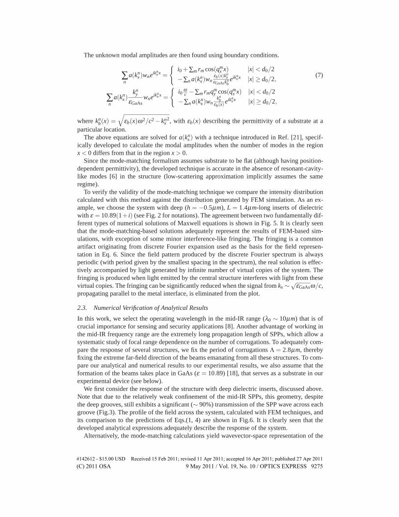
To verify the validity of the mode-matching technique we compare the intensity distributioncalculated with this method against the distribution generated by FEM simulation. As an ex-ample, we choose the system with deep (h = −0.5μm), L = 1.4μm-long inserts of dielectricwith ε = 10.89(1+ i) (see Fig. 2 for notations). The agreement between two fundamentally dif-ferent types of numerical solutions of Maxwell equations is shown in Fig. 5. It is clearly seenthat the mode-matching-based solutions adequately represent the results of FEM-based sim-ulations, with exception of some minor interference-like fringing. The fringing is a commonartifact originating from discrete Fourier expansion used as the basis for the field represen-tation in Eq. 6. Since the field pattern produced by the discrete Fourier spectrum is alwaysperiodic (with period given by the smallest spacing in the spectrum), the real solution is effec-tively accompanied by light generated by infinite number of virtual copies of the system. Thefringing is produced when light emitted by the central structure interferes with light from thesevirtual copies. The fringing can be significantly reduced when the signal from kx ∼√
εGaAsω/c,propagating parallel to the metal interface, is eliminated from the plot.
2.3. Numerical Verification of Analytical Results
In this work, we select the operating wavelength in the mid-IR range (λ0 ∼ 10μm) that is ofcrucial importance for sensing and security applications [8]. Another advantage of working inthe mid-IR frequency range are the extremely long propagation length of SPPs, which allow asystematic study of focal range dependence on the number of corrugations. To adequately com-pare the response of several structures, we fix the period of corrugations Λ = 2.8μm, therebyfixing the extreme far-field direction of the beams emanating from all these structures. To com-pare our analytical and numerical results to our experimental results, we also assume that theformation of the beams takes place in GaAs (ε = 10.89) [18], that serves as a substrate in ourexperimental device (see below).
We first consider the response of the structure with deep dielectric inserts, discussed above.Note that due to the relatively weak confinement of the mid-IR SPPs, this geometry, despitethe deep grooves, still exhibits a significant (∼ 90%) transmission of the SPP wave across eachgroove (Fig.3). The profile of the field across the system, calculated with FEM techniques, andits comparison to the predictions of Eqs.(1, 4) are shown in Fig.6. It is clearly seen that thedeveloped analytical expressions adequately describe the response of the system.
Alternatively, the mode-matching calculations yield wavevector-space representation of the
#142612 - $15.00 USD Received 15 Feb 2011; revised 11 Apr 2011; accepted 16 Apr 2011; published 27 Apr 2011(C) 2011 OSA 9 May 2011 / Vol. 19, No. 10 / OPTICS EXPRESS 9275
Fig. 5. Field profile, calculated with FEM simulations (top panels) and using the semi-analytical calculations (bottom) described in subsection 2.2; The parts of the spectrum cor-responding to propagation parallel to the structure, included in the calculations, are omittedfrom the plotting procedure to minimize fringing.
field that unambiguously demonstrates the dominant role of the interference of light scatteredby the SPPs in the optical response of the system.
To demonstrate universality of the observed phenomenon, we simulate the formation of thebeams in a similar system, where the relatively deep grooves are replaced with δ -like scatter-ers, modeled as 250nm-high and 100-nm-thick bumps. In contrast to the previously describedstructure, about 99% of SPP energy is transmitted through the individual δ -scatterer, so thecollective effect of the SPP bumps on the formation of the beams can be adequately evaluated.Fig.7 clearly reveals that the size of the focal zone is determined by the number of surfaceinhomogeneities contributing to the beam formation.
3. Experimental Set-Up and Results
Mid-IR plasmonic beam steering structures were fabricated in order to experimentally verifythe analytical and numerical simulations described above. The devices were fabricated usingstandard optical lithography and metallization techniques on semi-insulating GaAs wafers. Thefirst set of samples were fabricated to support mid-IR SPPs on the metal/GaAs interface [Fig.1(a)]. For these samples, the pattern for two periodic groove arrays, separated by 4.2μm wereexposed by photolithography in photoresist, which then served as an etch mask to define theperiod grooves (Λ = 2.8μm), etched a depth d=0.5μm into the GaAs surface. A second pho-toresist pattern, consisting of a single, 1.4μm slit, centered between the two groove arrays, wasthen exposed. A metal layer consisting of 10nm Ti and 200nm Au was deposited, and the cen-tral slit lifted off in acetone. The thin Ti layer is used to ensure adhesion of the metal layer tothe semiconductor surface, and does not significantly change the metal layer optical properties,as both Ti and Au, in the mid-IR wavelength range, have large and negative values of permittiv-ity [19]. The resulting structure consisted of the 1.4μm central slit, flanked by the two groovearrays of period 2.8μm. The GaAs wafer was then lapped down to a thickness of ∼ 200μm, andthe back surface roughened, to allow field measurements as close to the slit as possible and toprevent multiple reflections within the GaAs substrate, respectively (good agreement betweenexperimental results and theoretical calculations indicate that such roughening does not intro-duce major scattering in the system). A second set of samples was also fabricated, in this case to
#142612 - $15.00 USD Received 15 Feb 2011; revised 11 Apr 2011; accepted 16 Apr 2011; published 27 Apr 2011(C) 2011 OSA 9 May 2011 / Vol. 19, No. 10 / OPTICS EXPRESS 9276
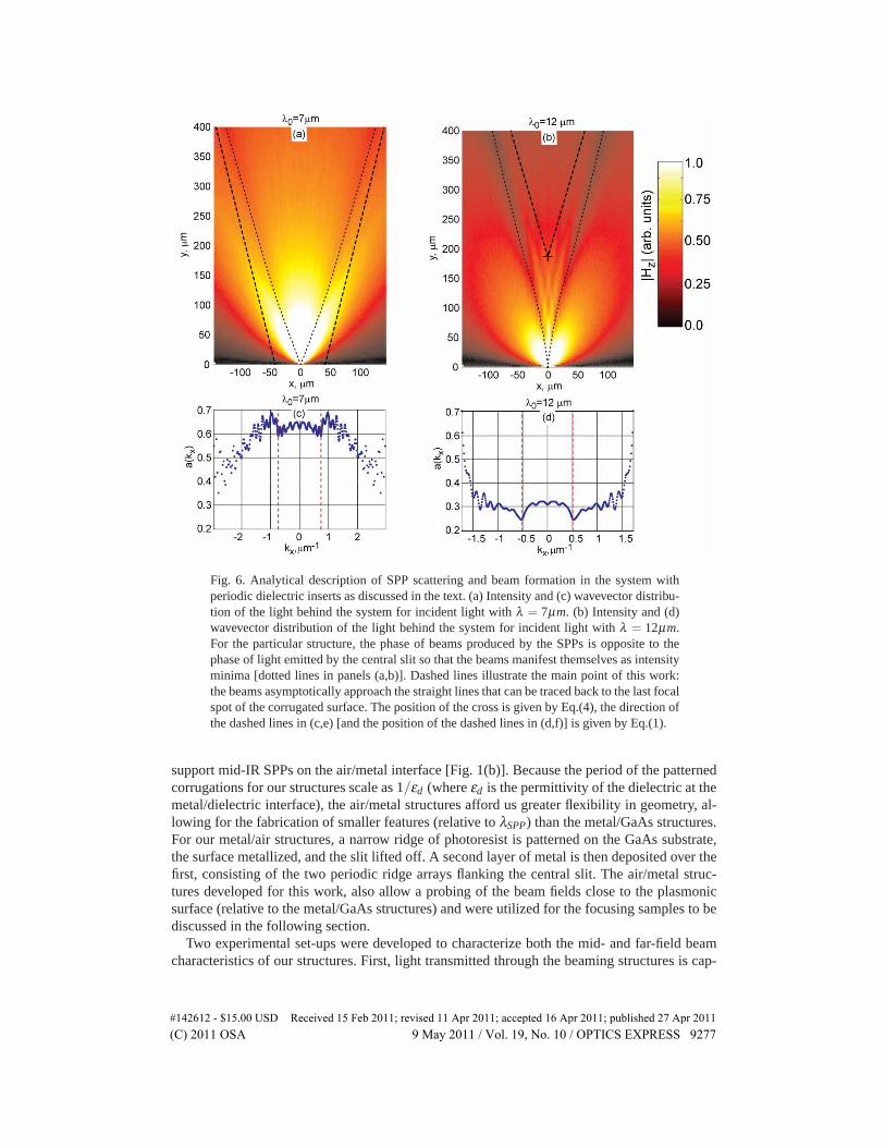
Fig. 6. Analytical description of SPP scattering and beam formation in the system withperiodic dielectric inserts as discussed in the text. (a) Intensity and (c) wavevector distribu-tion of the light behind the system for incident light with λ = 7μm. (b) Intensity and (d)wavevector distribution of the light behind the system for incident light with λ = 12μm.For the particular structure, the phase of beams produced by the SPPs is opposite to thephase of light emitted by the central slit so that the beams manifest themselves as intensityminima [dotted lines in panels (a,b)]. Dashed lines illustrate the main point of this work:the beams asymptotically approach the straight lines that can be traced back to the last focalspot of the corrugated surface. The position of the cross is given by Eq.(4), the direction ofthe dashed lines in (c,e) [and the position of the dashed lines in (d,f)] is given by Eq.(1).
support mid-IR SPPs on the air/metal interface [Fig. 1(b)]. Because the period of the patternedcorrugations for our structures scale as 1/εd (where εd is the permittivity of the dielectric at themetal/dielectric interface), the air/metal structures afford us greater flexibility in geometry, al-lowing for the fabrication of smaller features (relative to λSPP) than the metal/GaAs structures.For our metal/air structures, a narrow ridge of photoresist is patterned on the GaAs substrate,the surface metallized, and the slit lifted off. A second layer of metal is then deposited over thefirst, consisting of the two periodic ridge arrays flanking the central slit. The air/metal struc-tures developed for this work, also allow a probing of the beam fields close to the plasmonicsurface (relative to the metal/GaAs structures) and were utilized for the focusing samples to bediscussed in the following section.
Two experimental set-ups were developed to characterize both the mid- and far-field beamcharacteristics of our structures. First, light transmitted through the beaming structures is cap-
#142612 - $15.00 USD Received 15 Feb 2011; revised 11 Apr 2011; accepted 16 Apr 2011; published 27 Apr 2011(C) 2011 OSA 9 May 2011 / Vol. 19, No. 10 / OPTICS EXPRESS 9277
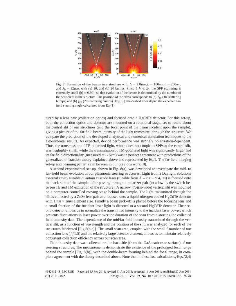
Fig. 7. Formation of the beams in a structure with Λ = 2.8μm,L = 100nm,h = 250nm,and λ0 = 12μm, with (a) 10, and (b) 20 bumps. Since L,h � λ0, the SPP scattering isextremely small (|t| � 0.99), so that evolution of the beams is determined by the number ofthe scatterers in the structure. The position of the cross corresponds to (a) f10 (10 scatteringbumps) and (b) f20 (20 scattering bumps) [Eq.(3)]; the dashed lines depict the expected far-field steering angle calculated from Eq.(1).
tured by a lens pair (collection optics) and focused onto a HgCdTe detector. For this set-up,both the collection optics and detector are mounted on a rotational stage, set to rotate aboutthe central slit of our structures (and the focal point of the beam incident upon the sample),giving a picture of the far-field beam intensity of the light transmitted through the structure. Wecompare the prediction of the developed analytical and numerical simulation techniques to theexperimental results. As expected, device performance was strongly polarization-dependent.Thus, the transmission of TE-polarized light, which does not couple to SPPs at the central slit,was negligibly small, while the transmission of TM-polarized light was significantly larger andits far-field directionality (measured at ∼ 5cm) was in perfect agreement with predictions of thegeneralized diffraction theory explained above and represented by Eq.1. The far-field imagingset-up and beaming patterns can be seen in our previous work [8].
A second experimental set-up, shown in Fig. 8(a), was developed to investigate the mid- tofar- field beam evolution in our plasmonic steering structures. Light from a Daylight Solutionsexternal cavity tunable quantum cascade laser (tunable from λ = 8.8−9.4μm) is focused ontothe back side of the sample, after passing through a polarizer pair (to allow us the switch be-tween TE and TM excitation of the structure). A narrow (75μm-wide) vertical slit was mountedon a computer-controlled moving stage behind the sample. The light transmitted through theslit is collected by a ZnSe lens pair and focused onto a liquid-nitrogen cooled HgCdTe detectorwith 1mm× 1mm element size. Finally a beam pick-off is placed before the focusing lens anda small fraction of the incident laser light is directed to a second HgCdTe detector. The sec-ond detector allows us to normalize the transmitted intensity to the incident laser power, whichprevents fluctuations in laser power over the duration of the scan from distorting the collectedfield intensity data. The dependence of the mid/far-field intensity transmitted through the ver-tical slit, as a function of wavelength and the position of the slit, was analyzed for each of thestructures fabricated [Fig.8(b,c)]. The small scan area, coupled with the small f-number of ourcollection lens ( f/1.5) and the relatively large detector element, allows us to maintain relativelyconsistent collection efficiency across our scan area.
Field intensity data was collected on the backside (from the GaAs substrate surface) of oursteering structures. The measurements demonstrate the existence of the prolonged focal rangebehind the sample [Fig. 8(b)], with the double-beam forming behind the focal range, in com-plete agreement with the theory described above. Note that in these last calculations, Eqs.(2,4)
#142612 - $15.00 USD Received 15 Feb 2011; revised 11 Apr 2011; accepted 16 Apr 2011; published 27 Apr 2011(C) 2011 OSA 9 May 2011 / Vol. 19, No. 10 / OPTICS EXPRESS 9278
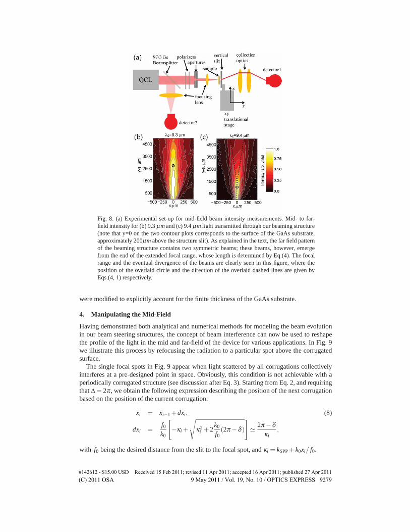
Fig. 8. (a) Experimental set-up for mid-field beam intensity measurements. Mid- to far-field intensity for (b) 9.3 μm and (c) 9.4 μm light transmitted through our beaming structure(note that y=0 on the two contour plots corresponds to the surface of the GaAs substrate,approximately 200μm above the structure slit). As explained in the text, the far field patternof the beaming structure contains two symmetric beams; these beams, however, emergefrom the end of the extended focal range, whose length is determined by Eq.(4). The focalrange and the eventual divergence of the beams are clearly seen in this figure, where theposition of the overlaid circle and the direction of the overlaid dashed lines are given byEqs.(4, 1) respectively.
were modified to explicitly account for the finite thickness of the GaAs substrate.
4. Manipulating the Mid-Field
Having demonstrated both analytical and numerical methods for modeling the beam evolutionin our beam steering structures, the concept of beam interference can now be used to reshapethe profile of the light in the mid and far-field of the device for various applications. In Fig. 9we illustrate this process by refocusing the radiation to a particular spot above the corrugatedsurface.
The single focal spots in Fig. 9 appear when light scattered by all corrugations collectivelyinterferes at a pre-designed point in space. Obviously, this condition is not achievable with aperiodically corrugated structure (see discussion after Eq. 3). Starting from Eq. 2, and requiringthat Δ = 2π , we obtain the following expression describing the position of the next corrugationbased on the position of the current corrugation:
xi = xi−1 +dxi, (8)
dxi =f0k0
[−κi +
√κ2
i +2k0
f0(2π −δ )
]� 2π −δ
κi,
with f0 being the desired distance from the slit to the focal spot, and κi = kSPP + k0xi/ f0.
#142612 - $15.00 USD Received 15 Feb 2011; revised 11 Apr 2011; accepted 16 Apr 2011; published 27 Apr 2011(C) 2011 OSA 9 May 2011 / Vol. 19, No. 10 / OPTICS EXPRESS 9279
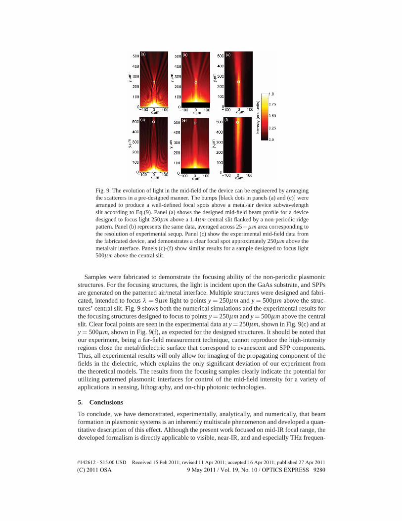
Fig. 9. The evolution of light in the mid-field of the device can be engineered by arrangingthe scatterers in a pre-designed manner. The bumps [black dots in panels (a) and (c)] werearranged to produce a well-defined focal spots above a metal/air device subwavelengthslit according to Eq.(9). Panel (a) shows the designed mid-field beam profile for a devicedesigned to focus light 250μm above a 1.4μm central slit flanked by a non-periodic ridgepattern. Panel (b) represents the same data, averaged across 25−μm area corresponding tothe resolution of experimental sequp. Panel (c) show the experimental mid-field data fromthe fabricated device, and demonstrates a clear focal spot approximately 250μm above themetal/air interface. Panels (c)-(f) show similar results for a sample designed to focus light500μm above the central slit.
Samples were fabricated to demonstrate the focusing ability of the non-periodic plasmonicstructures. For the focusing structures, the light is incident upon the GaAs substrate, and SPPsare generated on the patterned air/metal interface. Multiple structures were designed and fabri-cated, intended to focus λ = 9μm light to points y = 250μm and y = 500μm above the struc-tures’ central slit. Fig. 9 shows both the numerical simulations and the experimental results forthe focusing structures designed to focus to points y= 250μm and y= 500μm above the centralslit. Clear focal points are seen in the experimental data at y= 250μm, shown in Fig. 9(c) and aty = 500μm, shown in Fig. 9(f), as expected for the designed structures. It should be noted thatour experiment, being a far-field measurement technique, cannot reproduce the high-intensityregions close the metal/dielectric surface that correspond to evanescent and SPP components.Thus, all experimental results will only allow for imaging of the propagating component of thefields in the dielectric, which explains the only significant deviation of our experiment fromthe theoretical models. The results from the focusing samples clearly indicate the potential forutilizing patterned plasmonic interfaces for control of the mid-field intensity for a variety ofapplications in sensing, lithography, and on-chip photonic technologies.
5. Conclusions
To conclude, we have demonstrated, experimentally, analytically, and numerically, that beamformation in plasmonic systems is an inherently multiscale phenomenon and developed a quan-titative description of this effect. Although the present work focused on mid-IR focal range, thedeveloped formalism is directly applicable to visible, near-IR, and and especially THz frequen-
#142612 - $15.00 USD Received 15 Feb 2011; revised 11 Apr 2011; accepted 16 Apr 2011; published 27 Apr 2011(C) 2011 OSA 9 May 2011 / Vol. 19, No. 10 / OPTICS EXPRESS 9280

cies (where surface waves also propagate for long distances). The formalism can be furtherextended to predict the beam formation in new types of quantum cascade lasers [9], and inother structures where the emission pattern is formed by partial scattering of guided modes. Awide class of materials and devices where similar phenomena are expected to take place in-cludes photonic crystals, and other metamaterials- as well as composite structures with typicalinhomogeneity lengths scales comparable to wavelength.
6. Acknowledgements
This work was supported by ONR (# N00014-07-1-0457), NSF (#ECCS-0724763), AFRL(#FA8650-08-C-1445), and the AFOSR Young Investigator Program (#FA9550-10-1-0226).
#142612 - $15.00 USD Received 15 Feb 2011; revised 11 Apr 2011; accepted 16 Apr 2011; published 27 Apr 2011(C) 2011 OSA 9 May 2011 / Vol. 19, No. 10 / OPTICS EXPRESS 9281