Embed Size (px)
Citation preview
Fachgebiet 3D-Nanostrukturierung, Institut für Physik
Contact: [email protected]; [email protected]
Office: Unterpoerlitzer Straße 38 (Heisenbergbau) (tel: 3748) http://www.tu-ilmenau.de/3dnanostrukturierung/
Vorlesung: Friday 9:00 – 10:30, C 110
Übung: Friday (G), 11:00 – 12:30, C 110
Prof. Yong Lei & Dr. Yang Xu
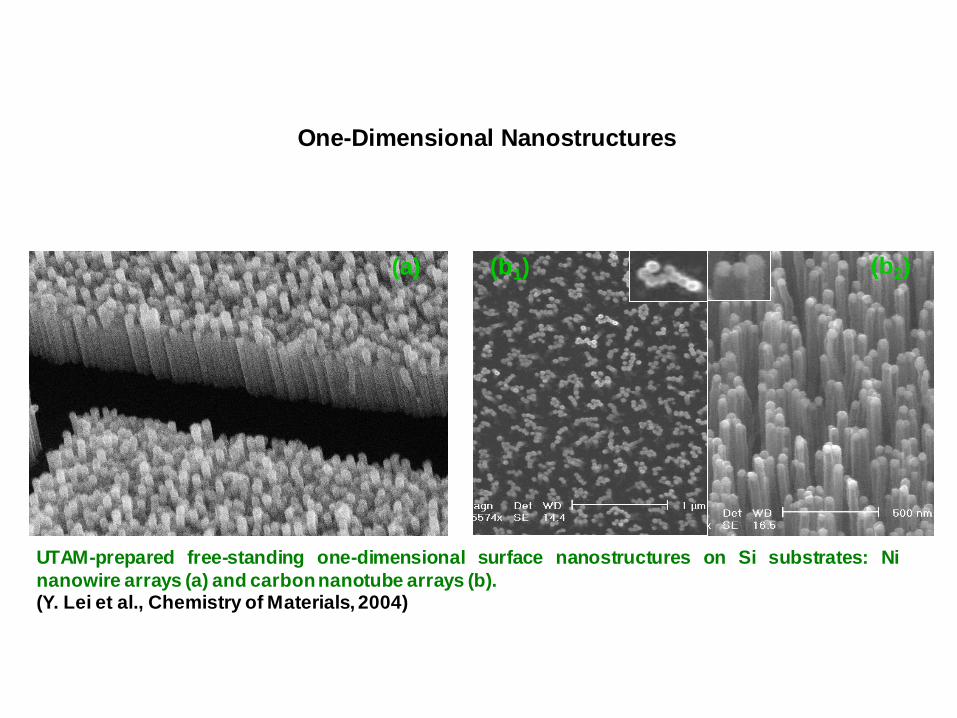
(a) (b2) (b1)
UTAM-prepared free-standing one-dimensional surface nanostructures on Si
substrates: Ni nanowire arrays (a) and carbon nanotube arrays (b).
Nanostrukturphysik (Nanostructure Physics)
Contents of Class 1
A general introduction of fundamentals of nano-
structured materials
Definition of nanostructures or nano-structured
materials
Significance of nanostructured materials
An outline of all the 12 classes
Characterization of nanostrcutures
3 types of nanostructures
Definition of nanocrystalline materials
‘There’s plenty of room at the bottom,
the principles of physics, as far as I can see, do not
speak against the possibility of manoeuvring things atom
by atom...’
By the legendary physicist Richard Feynman in 1959
(Feynman R., Eng Sci, 1960)
Progress made in past two decades has proven this
statement by the amazing nature of nanomaterials, has
achieved exciting technological advancement for the
benefit of mankind.
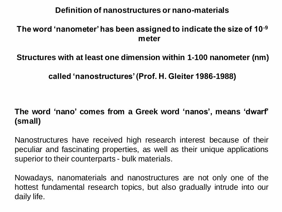
Definition of nanostructures or nano-materials
The word ‘nanometer’ has been assigned to indicate the size of 10-9
meter
Structures with at least one dimension within 1-100 nanometer (nm)
called ‘nanostructures’ (Prof. H. Gleiter 1986-1988)
The word ‘nano’ comes from a Greek word ‘nanos’, means ‘dwarf’
(small)
Nanostructures have received high research interest because of their
peculiar and fascinating properties, as well as their unique applications
superior to their counterparts - bulk materials.
Nowadays, nanomaterials and nanostructures are not only one of the
hottest fundamental research topics, but also gradually intrude into our
daily life.
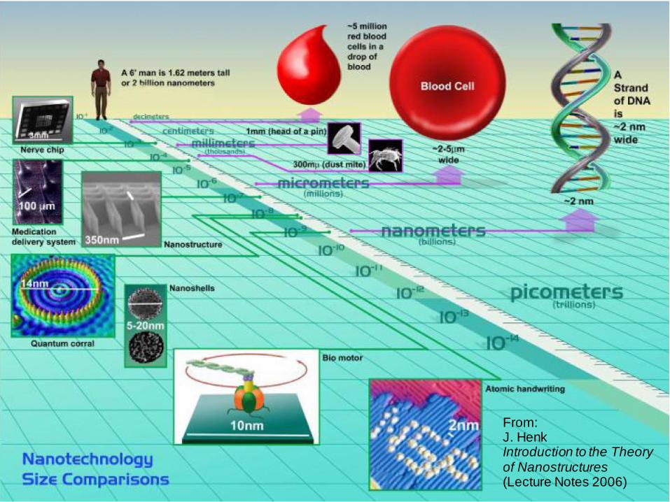
From: J. Henk Introduction to the Theory of Nanostructures (Lecture Notes 2006)
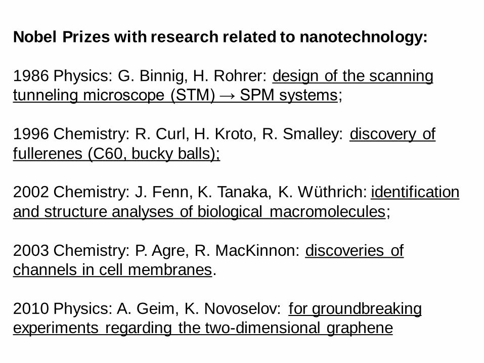
Nobel Prizes with research related to nanotechnology:
1986 Physics: G. Binnig, H. Rohrer: design of the scanning
tunneling microscope (STM) → SPM systems;
1996 Chemistry: R. Curl, H. Kroto, R. Smalley: discovery of
fullerenes (C60, bucky balls);
2002 Chemistry: J. Fenn, K. Tanaka, K. Wüthrich: identification
and structure analyses of biological macromolecules;
2003 Chemistry: P. Agre, R. MacKinnon: discoveries of
channels in cell membranes.
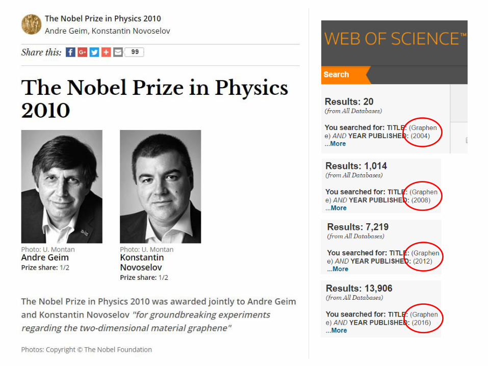
2010 Physics: A. Geim, K. Novoselov: for groundbreaking
experiments regarding the two-dimensional graphene
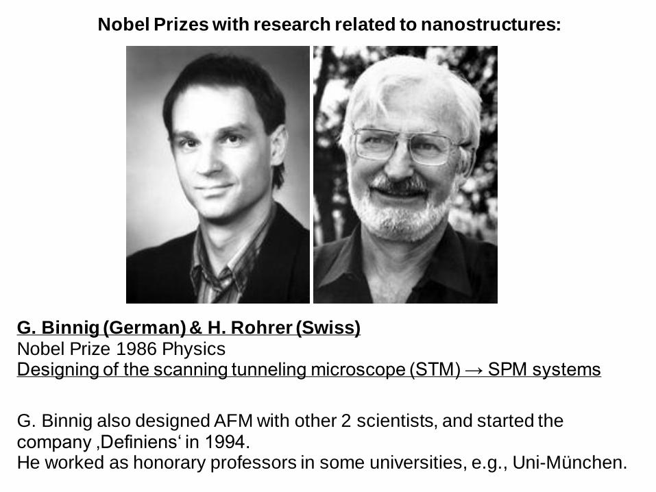
G. Binnig (German) & H. Rohrer (Swiss) Nobel Prize 1986 Physics Designing of the scanning tunneling microscope (STM) → SPM systems
Nobel Prizes with research related to nanostructures:
G. Binnig also designed AFM with other 2 scientists, and started the company ‚Definiens‘ in 1994. He worked as honorary professors in some universities, e.g., Uni-München.
8
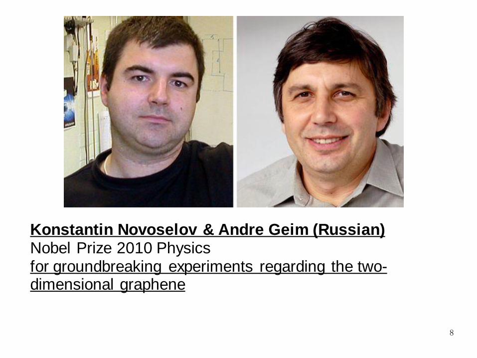
Konstantin Novoselov & Andre Geim (Russian) Nobel Prize 2010 Physics for groundbreaking experiments regarding the two-dimensional graphene
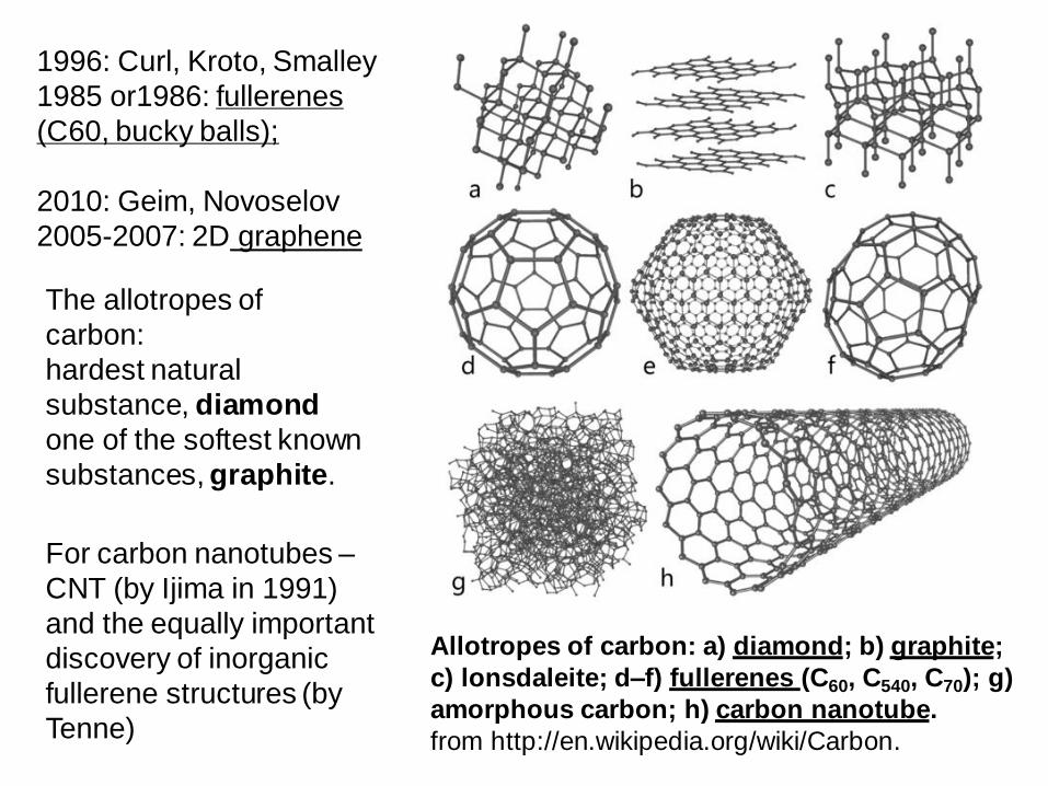
For carbon nanotubes –
CNT (by Ijima in 1991)
and the equally important
discovery of inorganic
fullerene structures (by
Tenne)
1996: Curl, Kroto, Smalley
1985 or1986: fullerenes
(C60, bucky balls);
2010: Geim, Novoselov
2005-2007: 2D graphene
The allotropes of
carbon:
hardest natural
substance, diamond
one of the softest known
substances, graphite.
Allotropes of carbon: a) diamond; b) graphite;
c) lonsdaleite; d–f) fullerenes (C60, C540, C70); g)
amorphous carbon; h) carbon nanotube.
from http://en.wikipedia.org/wiki/Carbon.
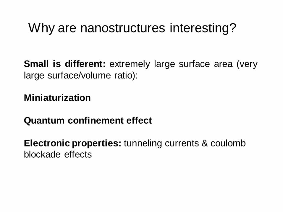
Why are nanostructures interesting?
Small is different: extremely large surface area (very
large surface/volume ratio):
Miniaturization
Quantum confinement effect
Electronic properties: tunneling currents & coulomb
blockade effects
Miniaturization represent the trend in different technologies:
simply by down-sizing existing microstructures into 1-100
nm range:
most successful example is microelectronics, where
‘smaller‘ means greater performance (since the invention of
integrated circuits);
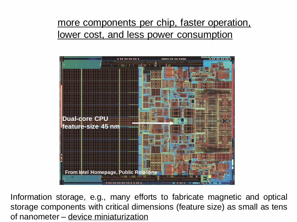
From Intel Homepage, Public Relations
Dual-core CPU
feature-size 45 nm
more components per chip, faster operation,
lower cost, and less power consumption
Information storage, e.g., many efforts to fabricate magnetic and optical
storage components with critical dimensions (feature size) as small as tens
of nanometer – device miniaturization
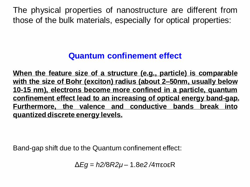
Quantum confinement effect
When the feature size of a structure (e.g., particle) is comparable
with the size of Bohr (exciton) radius (about 2–50nm, usually below
10-15 nm), electrons become more confined in a particle, quantum
confinement effect lead to an increasing of optical energy band-gap.
Furthermore, the valence and conductive bands break into
quantized discrete energy levels.
Band-gap shift due to the Quantum confinement effect:
ΔEg = h2/8R2μ – 1.8e2 /4πεoεR
The physical properties of nanostructure are different from
those of the bulk materials, especially for optical properties:
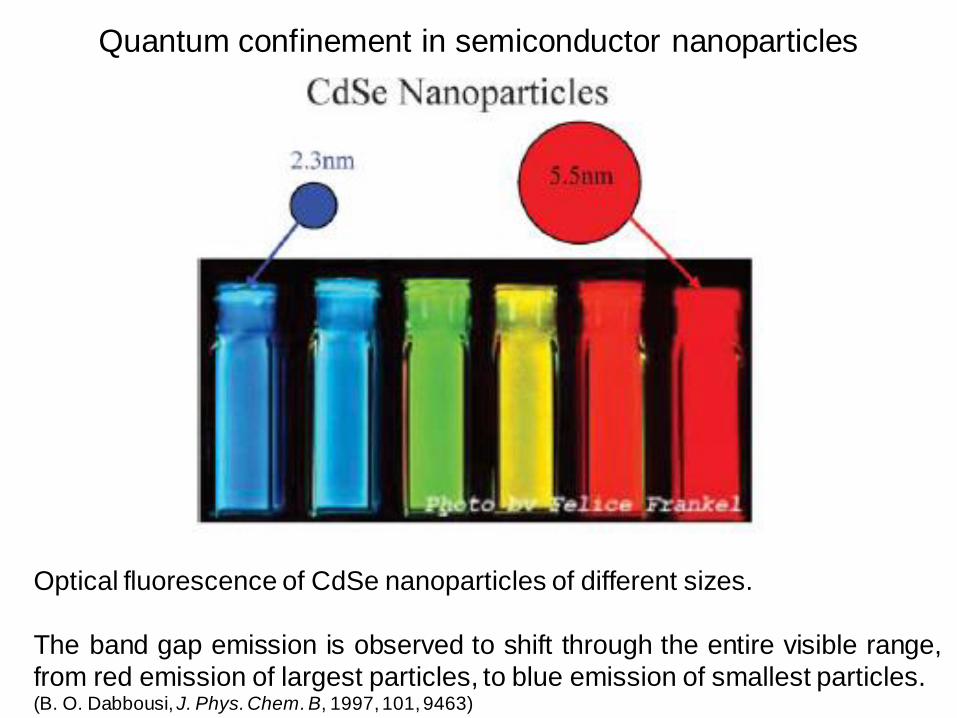
Quantum confinement in semiconductor nanoparticles
Optical fluorescence of CdSe nanoparticles of different sizes.
The band gap emission is observed to shift through the entire visible range,
from red emission of largest particles, to blue emission of smallest particles. (B. O. Dabbousi, J. Phys. Chem. B, 1997, 101, 9463)
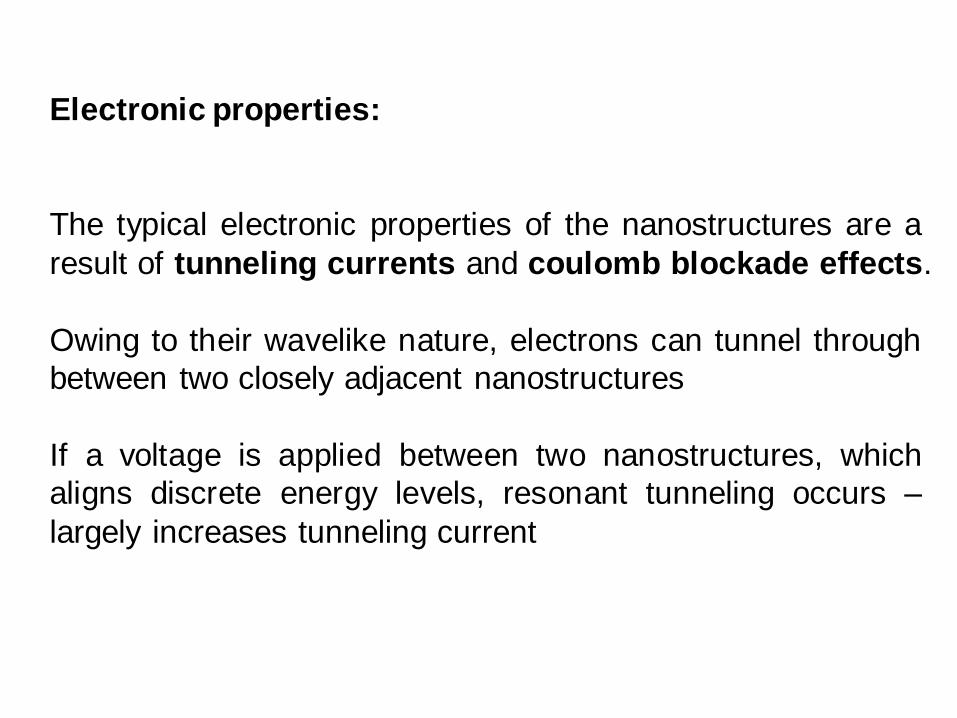
Electronic properties:
The typical electronic properties of the nanostructures are a
result of tunneling currents and coulomb blockade effects.
Owing to their wavelike nature, electrons can tunnel through
between two closely adjacent nanostructures
If a voltage is applied between two nanostructures, which
aligns discrete energy levels, resonant tunneling occurs –
largely increases tunneling current
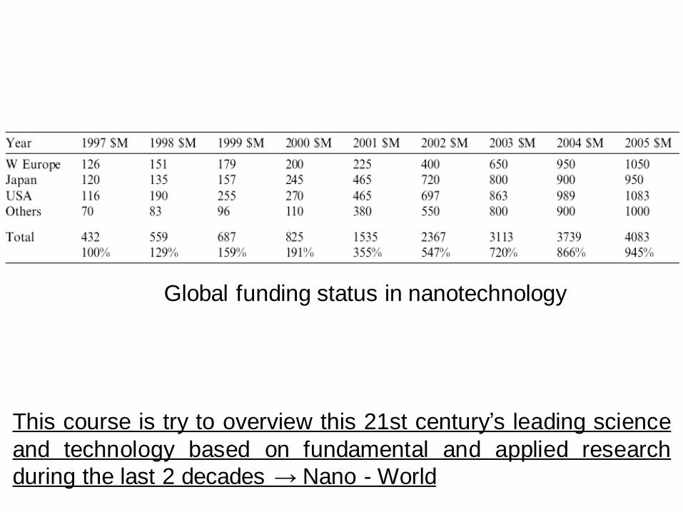
Global funding status in nanotechnology
This course is try to overview this 21st century’s leading science
and technology based on fundamental and applied research
during the last 2 decades → Nano - World
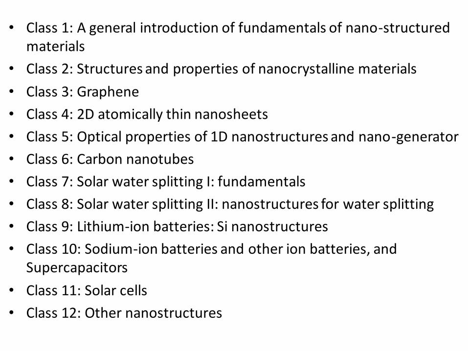
• Class 1: A general introduction of fundamentals of nano-structured materials
• Class 2: Structures and properties of nanocrystalline materials
• Class 3: Graphene
• Class 4: 2D atomically thin nanosheets
• Class 5: Optical properties of 1D nanostructures and nano-generator
• Class 6: Carbon nanotubes
• Class 7: Solar water splitting I: fundamentals
• Class 8: Solar water splitting II: nanostructures for water splitting
• Class 9: Lithium-ion batteries: Si nanostructures
• Class 10: Sodium-ion batteries and other ion batteries, and Supercapacitors
• Class 11: Solar cells
• Class 12: Other nanostructures
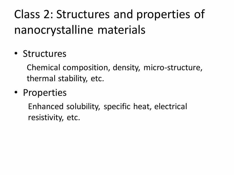
Class 2: Structures and properties of nanocrystalline materials
• Structures
Chemical composition, density, micro-structure, thermal stability, etc.
• Properties
Enhanced solubility, specific heat, electrical resistivity, etc.
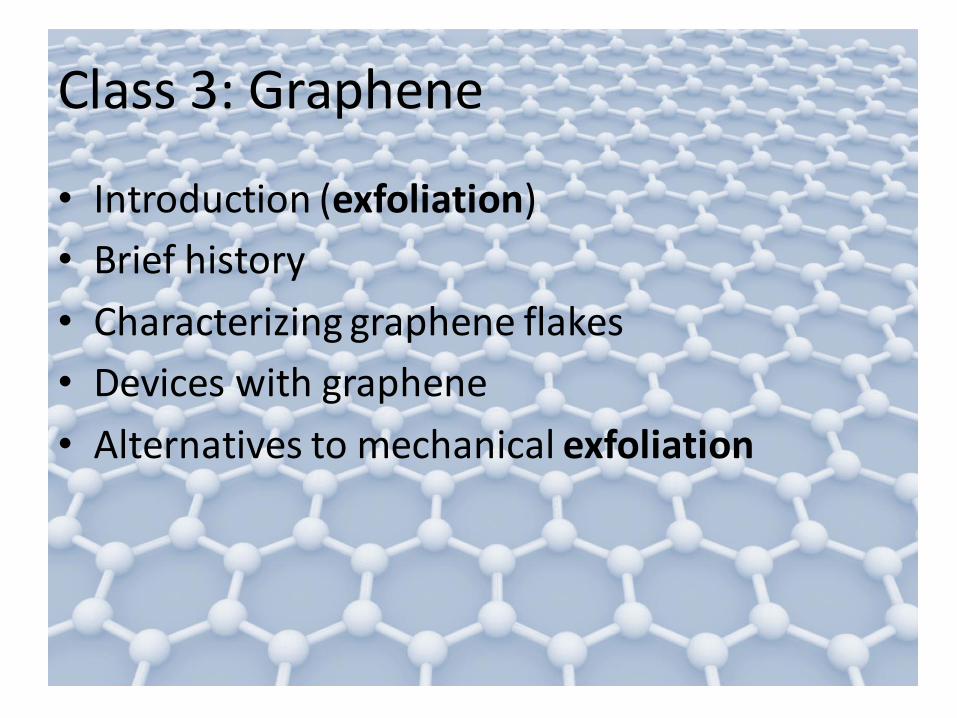
Class 3: Graphene
• Introduction (exfoliation)
• Brief history
• Characterizing graphene flakes
• Devices with graphene
• Alternatives to mechanical exfoliation
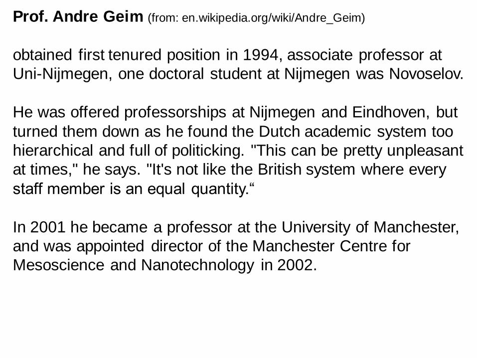
Prof. Andre Geim (from: en.wikipedia.org/wiki/Andre_Geim)
obtained first tenured position in 1994, associate professor at
Uni-Nijmegen, one doctoral student at Nijmegen was Novoselov.
He was offered professorships at Nijmegen and Eindhoven, but
turned them down as he found the Dutch academic system too
hierarchical and full of politicking. "This can be pretty unpleasant
at times," he says. "It's not like the British system where every
staff member is an equal quantity.“
In 2001 he became a professor at the University of Manchester,
and was appointed director of the Manchester Centre for
Mesoscience and Nanotechnology in 2002.
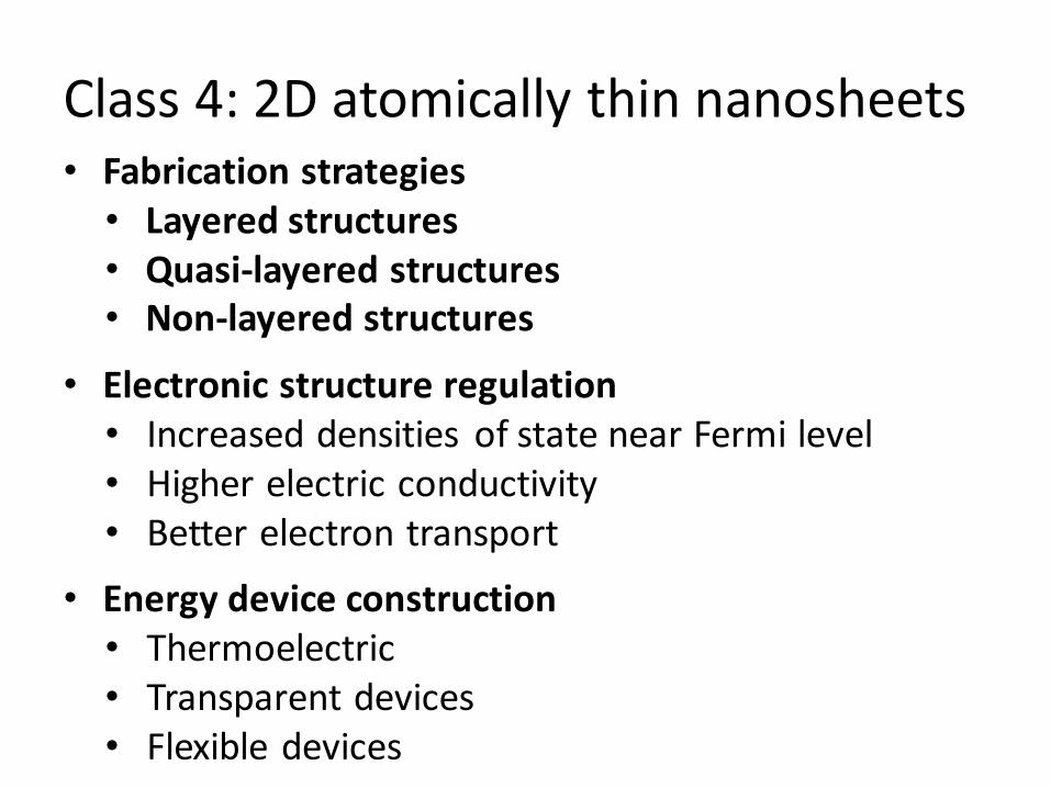
Class 4: 2D atomically thin nanosheets • Fabrication strategies
• Layered structures • Quasi-layered structures • Non-layered structures
• Electronic structure regulation • Increased densities of state near Fermi level • Higher electric conductivity • Better electron transport
• Energy device construction • Thermoelectric • Transparent devices • Flexible devices
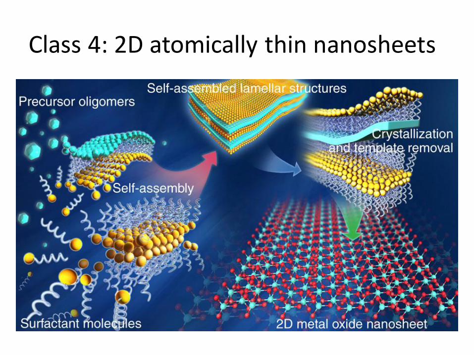
Class 4: 2D atomically thin nanosheets
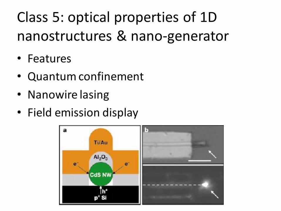
Class 5: optical properties of 1D nanostructures & nano-generator
• Features
• Quantum confinement
• Nanowire lasing
• Field emission display
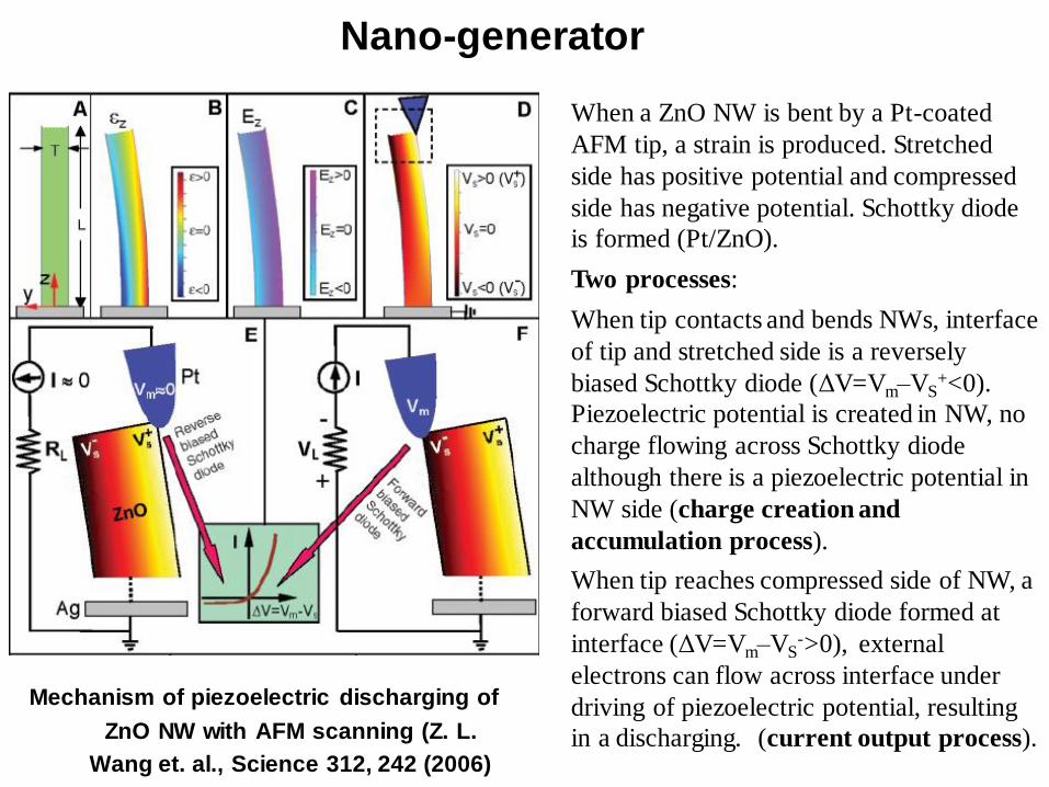
Mechanism of piezoelectric discharging of
ZnO NW with AFM scanning (Z. L.
Wang et. al., Science 312, 242 (2006)
When a ZnO NW is bent by a Pt-coated
AFM tip, a strain is produced. Stretched
side has positive potential and compressed
side has negative potential. Schottky diode
is formed (Pt/ZnO).
Two processes:
When tip contacts and bends NWs, interface
of tip and stretched side is a reversely
biased Schottky diode (ΔV=Vm–VS+<0).
Piezoelectric potential is created in NW, no
charge flowing across Schottky diode
although there is a piezoelectric potential in
NW side (charge creation and
accumulation process).
When tip reaches compressed side of NW, a
forward biased Schottky diode formed at
interface (ΔV=Vm–VS->0), external
electrons can flow across interface under
driving of piezoelectric potential, resulting
in a discharging. (current output process).
Nano-generator
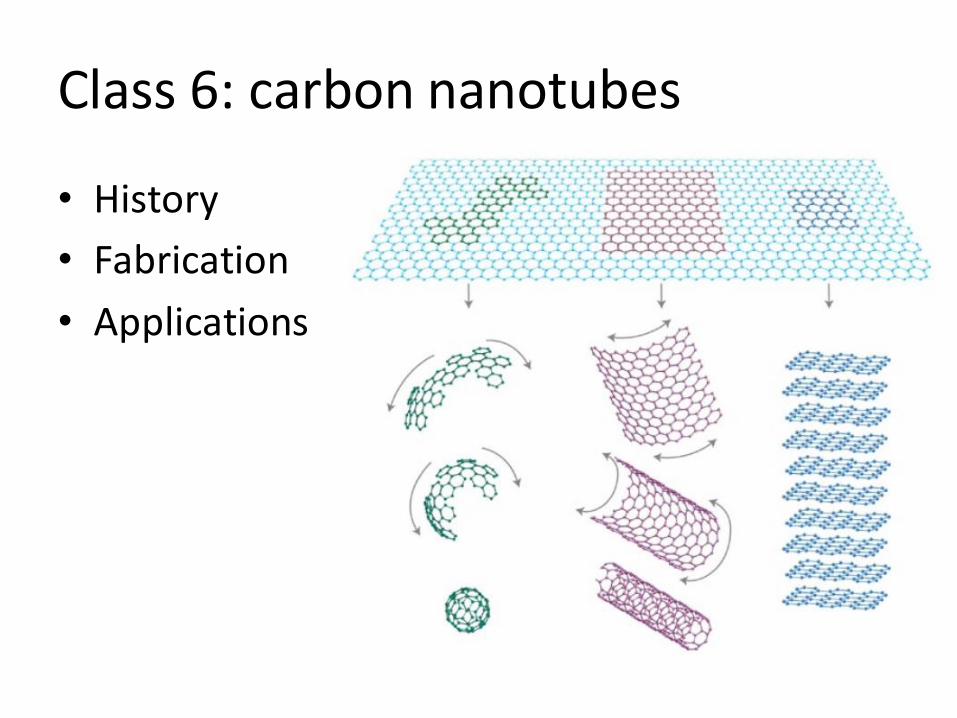
Class 6: carbon nanotubes
• History
• Fabrication
• Applications
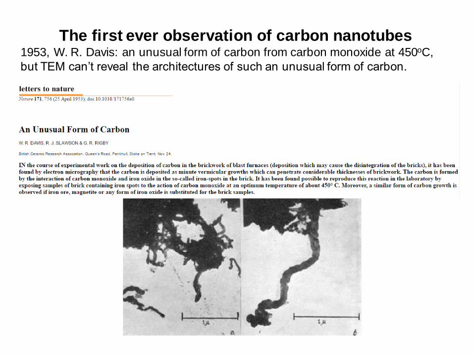
The first ever observation of carbon nanotubes 1953, W. R. Davis: an unusual form of carbon from carbon monoxide at 450oC,
but TEM can’t reveal the architectures of such an unusual form of carbon.
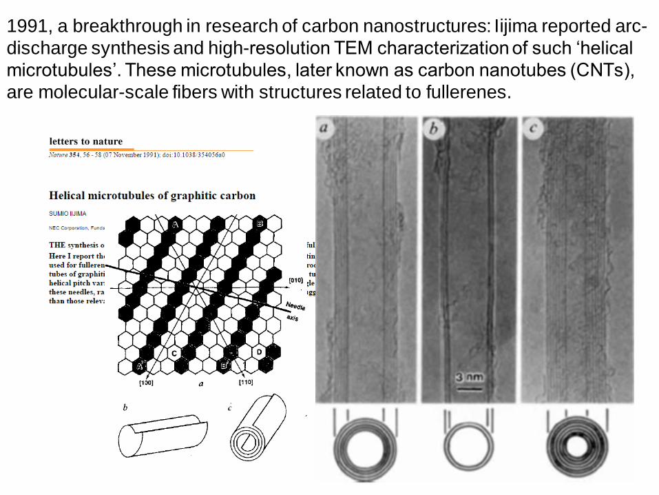
1991, a breakthrough in research of carbon nanostructures: Iijima reported arc-
discharge synthesis and high-resolution TEM characterization of such ‘helical
microtubules’. These microtubules, later known as carbon nanotubes (CNTs),
are molecular-scale fibers with structures related to fullerenes.
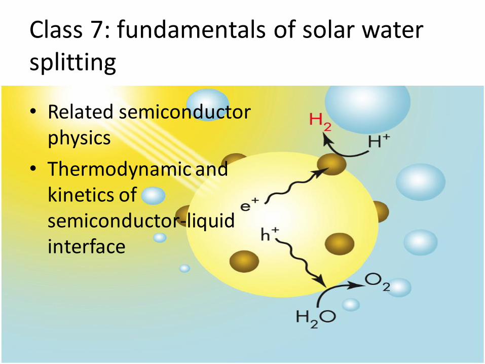
Class 7: fundamentals of solar water splitting
• Related semiconductor physics
• Thermodynamic and kinetics of semiconductor-liquid interface
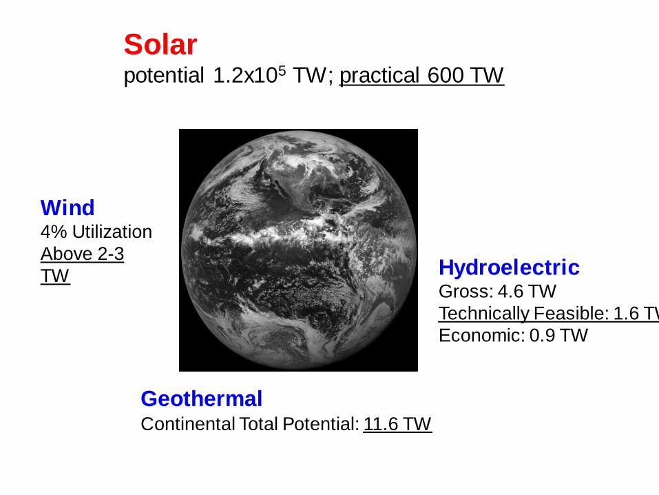
Hydroelectric Gross: 4.6 TW
Technically Feasible: 1.6 TW
Economic: 0.9 TW
Geothermal Continental Total Potential: 11.6 TW
Wind 4% Utilization
Above 2-3
TW
Solar potential 1.2x10⁵ TW; practical 600 TW
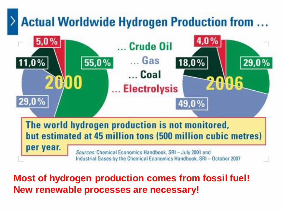
Most of hydrogen production comes from fossil fuel!
New renewable processes are necessary!
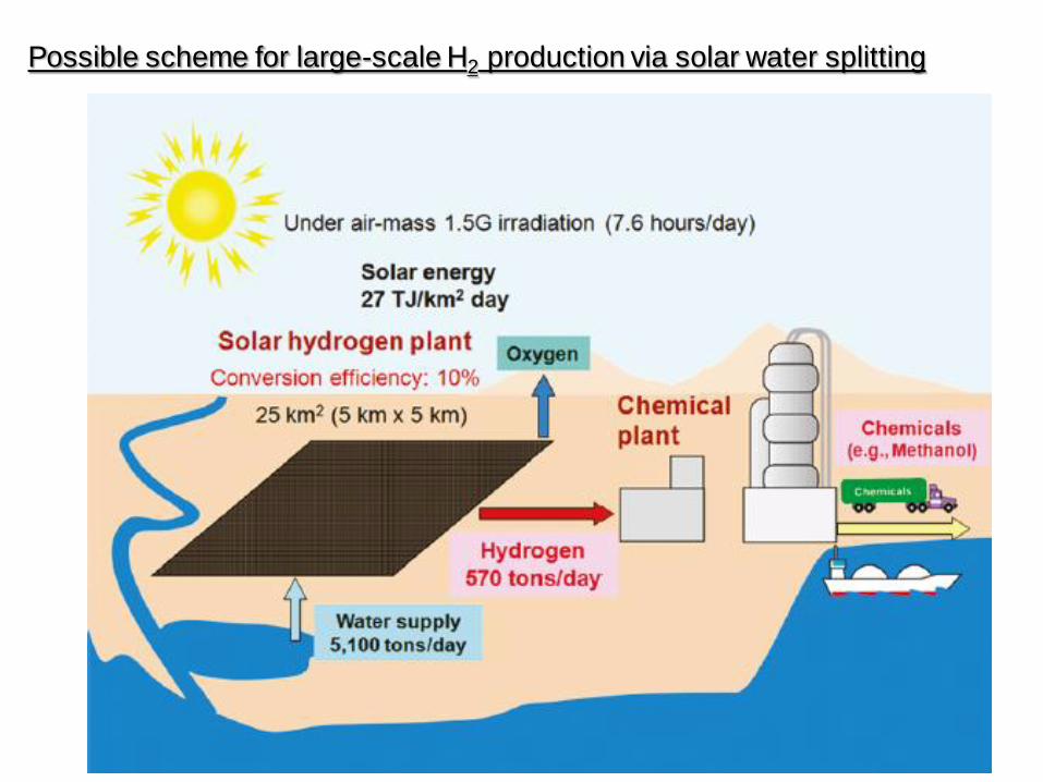
Possible scheme for large-scale H2 production via solar water splitting
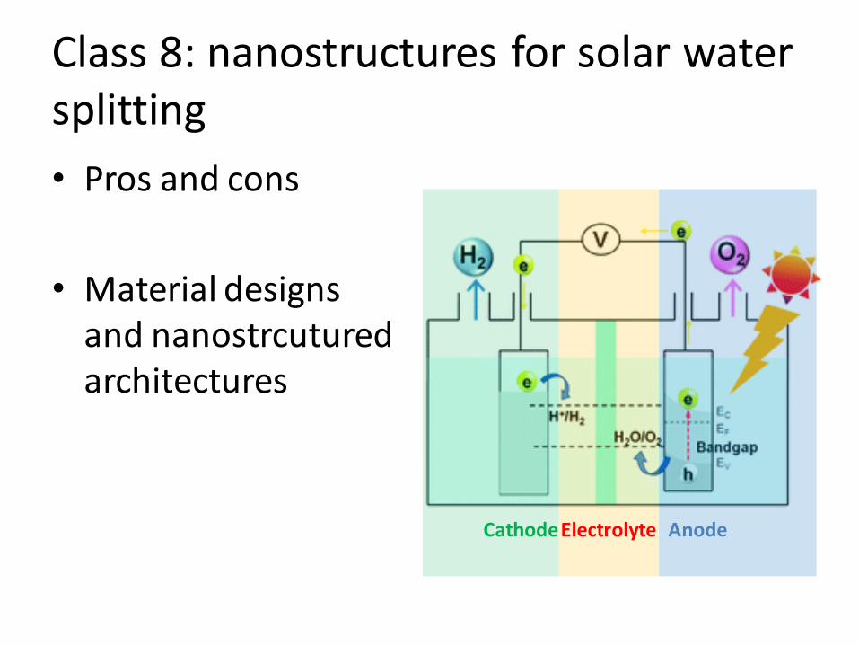
Class 8: nanostructures for solar water splitting
• Pros and cons
• Material designs and nanostrcutured architectures
Anode Cathode Electrolyte
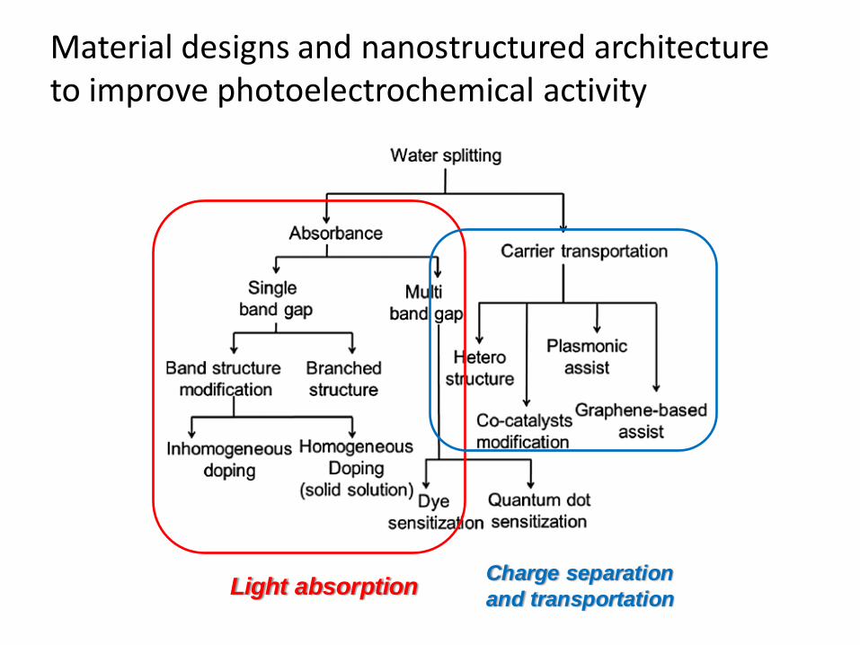
Material designs and nanostructured architecture to improve photoelectrochemical activity
Light absorption Charge separation
and transportation
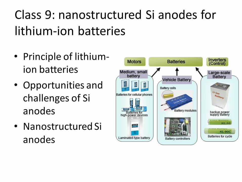
Class 9: nanostructured Si anodes for lithium-ion batteries
• Principle of lithium-ion batteries
• Opportunities and challenges of Si anodes
• Nanostructured Si anodes
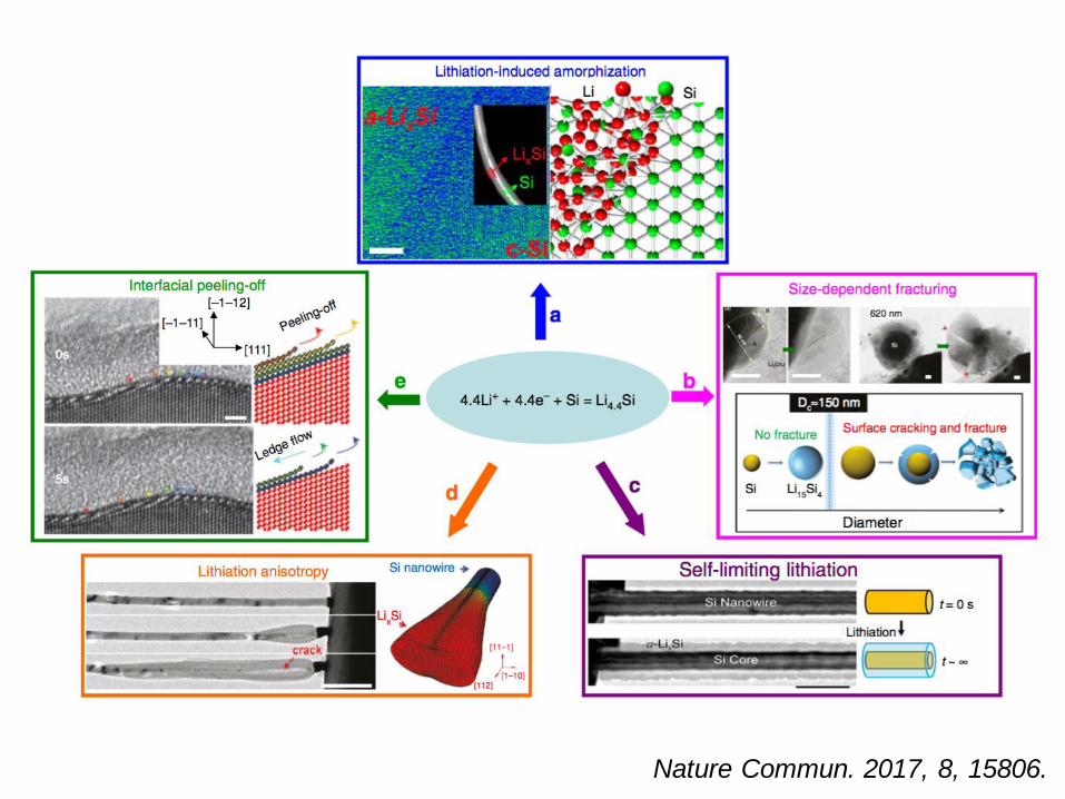
Nature Commun. 2017, 8, 15806.
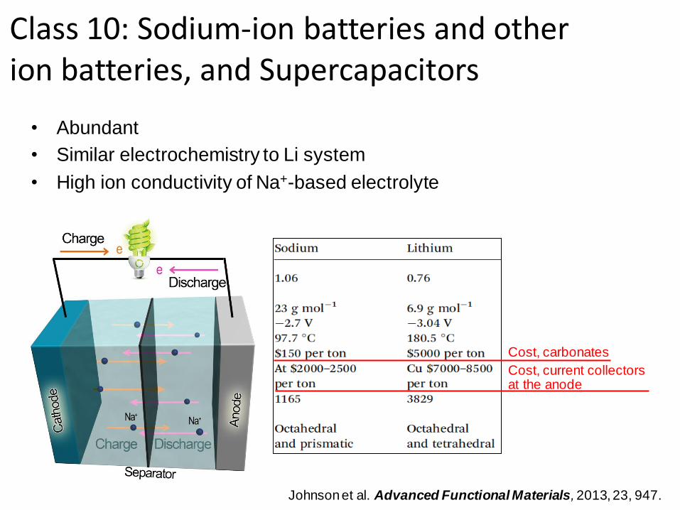
• Abundant
• Similar electrochemistry to Li system
• High ion conductivity of Na+-based electrolyte
Johnson et al. Advanced Functional Materials, 2013, 23, 947.
Cost, carbonates
Cost, current collectors at the anode
Class 10: Sodium-ion batteries and other ion batteries, and Supercapacitors
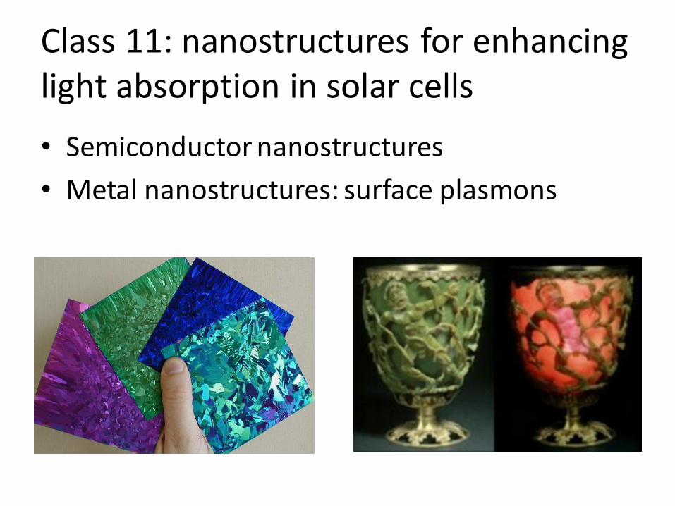
Class 11: nanostructures for enhancing light absorption in solar cells
• Semiconductor nanostructures
• Metal nanostructures: surface plasmons
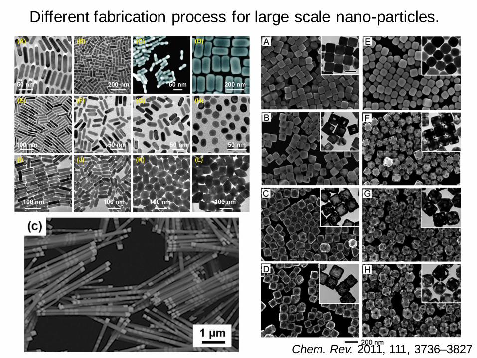
Different fabrication process for large scale nano-particles.
Chem. Rev. 2011, 111, 3736–3827
Characterization of nano-strcutures
An appropriate characterization will play a crucial role in determining
various structures and properties of nanostructures.
Three broadly approved aspects of characterization are
1. Morphology
2. Crystalline structure
3. Chemical analysis
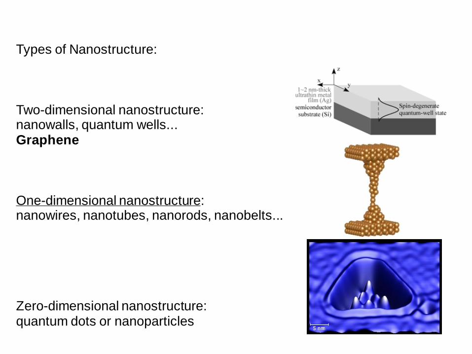
Types of Nanostructure: Two-dimensional nanostructure: nanowalls, quantum wells... Graphene One-dimensional nanostructure: nanowires, nanotubes, nanorods, nanobelts... Zero-dimensional nanostructure: quantum dots or nanoparticles
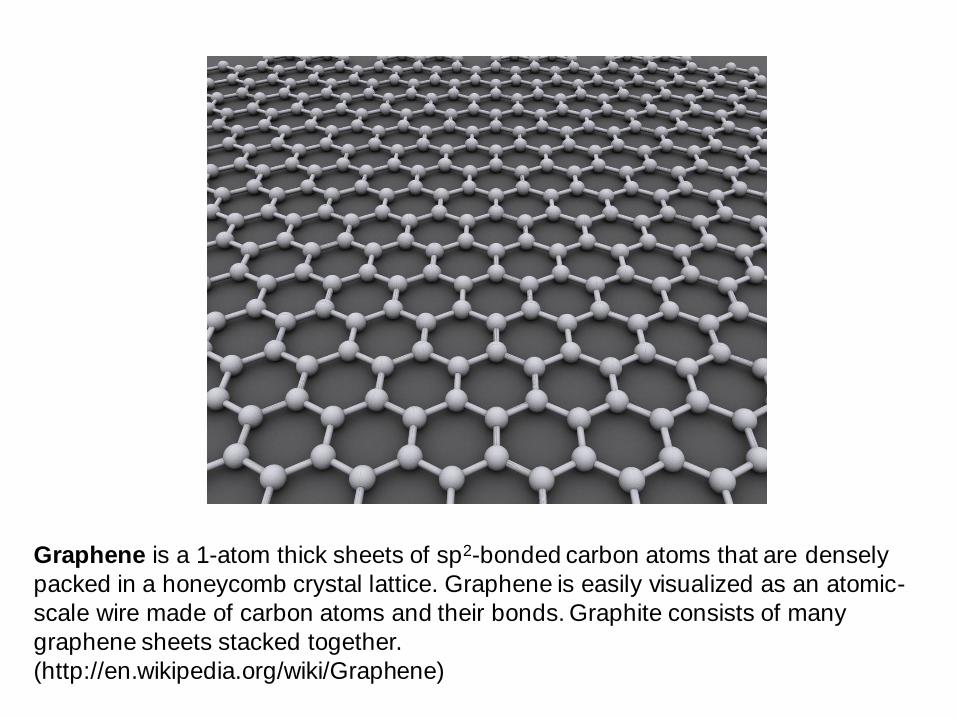
Graphene is a 1-atom thick sheets of sp2-bonded carbon atoms that are densely
packed in a honeycomb crystal lattice. Graphene is easily visualized as an atomic-
scale wire made of carbon atoms and their bonds. Graphite consists of many
graphene sheets stacked together.
(http://en.wikipedia.org/wiki/Graphene)
One dimensional (1D) nanostructures
1D nanostructure: nanowires, nanotubes, nanorods...
1D nanostructure refers to the systems with the lateral
dimension in the range of 1-100 nm.
Compared to 0D nanostructures, 1D nanostructures
provides a better model system to investigate the
dependence of properties (electronic transport, optical
& mechanical) on size confinement and dimension.
Nanowires, in particular, plays an important role as
both interconnects and active components in
preparing nanoscale devices (Nano-devices).
One-Dimensional Nanostructures
(a) (b2) (b1)
UTAM-prepared free-standing one-dimensional surface nanostructures on Si substrates: Ni
nanowire arrays (a) and carbon nanotube arrays (b). (Y. Lei et al., Chemistry of Materials, 2004)
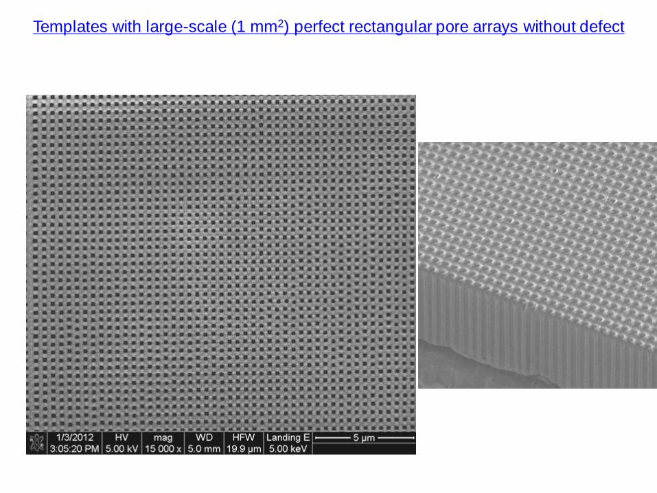
Templates with large-scale (1 mm2) perfect rectangular pore arrays without defect
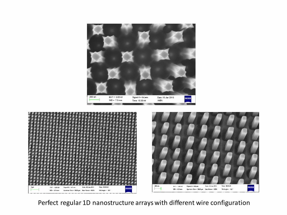
Perfect regular 1D nanostructure arrays with different wire configuration
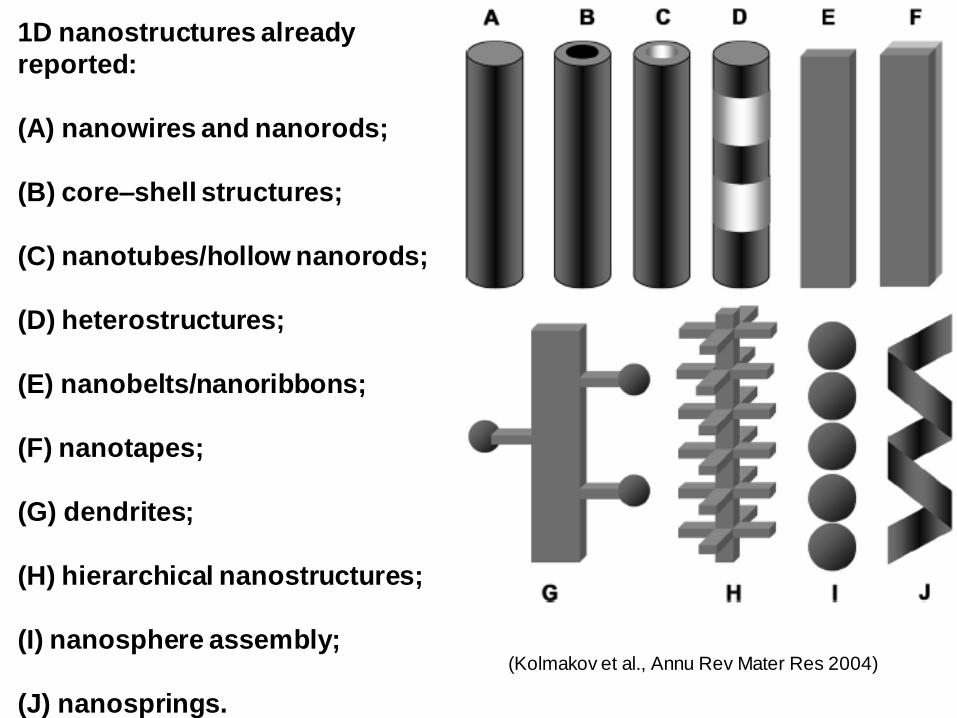
1D nanostructures already
reported:
(A) nanowires and nanorods;
(B) core–shell structures;
(C) nanotubes/hollow nanorods;
(D) heterostructures;
(E) nanobelts/nanoribbons;
(F) nanotapes;
(G) dendrites;
(H) hierarchical nanostructures;
(I) nanosphere assembly;
(J) nanosprings.
(Kolmakov et al., Annu Rev Mater Res 2004)
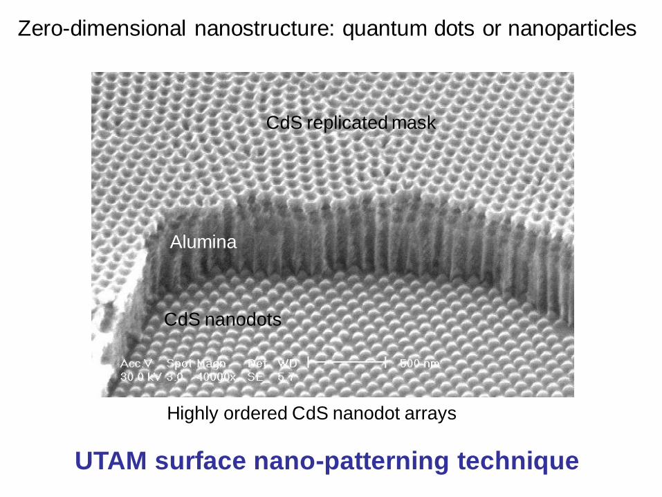
Highly ordered CdS nanodot arrays
CdS replicated mask
Alumina
CdS nanodots
Zero-dimensional nanostructure: quantum dots or nanoparticles
UTAM surface nano-patterning technique

• Class 1: A general introduction of fundamentals of nano-structured materials
• Class 2: Structures and properties of nanocrystalline materials
• Class 3: Graphene
• Class 4: 2D atomically thin nanosheets
• Class 5: Optical properties of 1D nanostructures and nano-generator
• Class 6: Carbon nanotubes
• Class 7: Solar water splitting I: fundamentals
• Class 8: Solar water splitting II: nanostructures for water splitting
• Class 9: Lithium-ion batteries: Si nanostructures
• Class 10: Sodium-ion batteries and other ion batteries, and Supercapacitors
• Class 11: Solar cells
• Class 12: Other nanostructures

Thanks for your attention


![Movement of Atoms [Sound, Phonons] Brockhouse 1950... E Q π/a The Nobel Prize in Physics 1994 Phonon Spectroscopy: 1) neutrons 2) high resolution X-rays](https://img.pdfslide.tips/doc/110x75/55147c8a550346ea6e8b4752/movement-of-atoms-sound-phonons-brockhouse-1950-e-q-a-the-nobel-prize-in-physics-1994-phonon-spectroscopy-1-neutrons-2-high-resolution-x-rays.jpg)


![Quantenchemische Studie der Photophysik eines kationischen ... · Nobel Prize winners in Physics Isamu Akasaki, Hiroshi Amano and Shuji Nakamura who have developed blue LED [2]. In](https://img.pdfslide.tips/doc/110x75/5dd0daa8d6be591ccb6305f4/quantenchemische-studie-der-photophysik-eines-kationischen-nobel-prize-winners.jpg)