Embed Size (px)
Citation preview
Research Article
Sadia Muniza Faraz*, Syed Riaz un Nabi Jafri, Hashim Raza Khan, Wakeel Shah,Naveed ul Hassan Alvi, Qamar ul Wahab, and Omer Nur
Effect of annealing temperature on the interfacestate density of n-ZnO nanorod/p-Siheterojunction diodes
https://doi.org/10.1515/phys-2021-0053received February 19, 2021; accepted June 19, 2021
Abstract: The effect of post-growth annealing treatmentof zinc oxide (ZnO) nanorods on the electrical propertiesof their heterojunction diodes (HJDs) is investigated. ZnOnanorods are synthesized by the low-temperature aqu-eous solution growth technique and annealed at tem-peratures of 400 and 600°C. The as-grown and annealednanorods are studied by scanning electron microscopy(SEM) and photoluminescence (PL) spectroscopy. Electricalcharacterization of the ZnO/Si heterojunction diode is doneby current–voltage (I–V) and capacitance–voltage (C–V)measurements at room temperature. The barrier height(ϕB), ideality factor (n), doping concentration and densityof interface states (NSS) are extracted. All HJDs exhibited anonlinear behavior with rectification factors of 23, 1,596and 309 at ±5 V for the as-grown, 400 and 600°C-annealednanorod HJDs, respectively. Barrier heights of 0.81 and0.63 V are obtained for HJDs of 400 and 600°C-annealednanorods, respectively. The energy distribution of the inter-face state density has been investigated and found to be inthe range 0.70 × 10¹⁰ to 1.05 × 10¹² eV/cm2 below the con-duction band from EC = 0.03 to EC = 0.58 eV. The highestdensity of interface states is observed in HJDs of 600°C-annealed nanorods. Overall improved behavior is observed
for the heterojunctions diodes of 400°C-annealed ZnOnanorods.
Keywords: ZnO nanorods, heterojunction, annealing, elec-trical characterization, interface states
1 Introduction
Zinc oxide (ZnO) is a direct and wide band-gap semicon-ductor (3.37 eV) studied widely for electronic and optoelec-tronic applications, such as light-emitting diodes, sensors,thin-film transistor (TFT), solar cells and UV photodetectors[1–3].
Zinc oxide shows n-type conductivity without anyintentional doping and obtaining reproducible p-dopedZnO is very challenging. Therefore, its heterojunctionsare realized on a variety of p-doped substrates such asSi, GaN, SiC, CuO2, etc. [4–8]. Among these, ZnO/Si hetero-junctions have attracted a great deal of interest due tolow cost and fewer process steps. The heterojunctions ofZnO nanorods/Si are very flexible in fabrication but theirelectronic and optical properties are strongly influencedby the presence of point defects and strains contained inZnO nanorods (NR) grown at low temperature. Since hetero-junctions are widely employed as fundamental buildingblocks of several devices, therefore, growth of defect-freepatterned and aligned one-dimensional nanorods with betteroptical quality is very important for the realization of efficientZnO/Si heterojunction and other nanodevices [9–12].
Thermal treatment is a conventional and effectivetechnique for reducing strains and defects and improvingthe crystalline quality [13,14]. The structural and opticalproperties of ZnO/Si heterojunctions can be modulatedby controlling the growth temperature and thermalannealing atmosphere and conditions of ZnO nanorods(NR) [15,16]. Low defect concentration, high crystallinityand improved current–voltage (I–V) characteristics havebeen recently reported for ZnO/Si heterojunction diodes
* Corresponding author: Sadia Muniza Faraz, Department ofElectronic Engineering, NED University of Engineering andTechnology, Karachi 75270, Pakistan, e-mail: [email protected] Riaz un Nabi Jafri, Hashim Raza Khan, Wakeel Shah:Department of Electronic Engineering, NED University of Engineeringand Technology, Karachi 75270, PakistanNaveed ul Hassan Alvi: RISE Research Institutes of Sweden,Bredgatan 33, Norrkőping, SwedenQamar ul Wahab: Departments of Physics, Chemistry and Biology(IFM), Linköping University, Linköping, SwedenOmer Nur: Department of Science and Technology (ITN), Faculty ofScience & Engineering, Linköping University, Linköping, Sweden
Open Physics 2021; 19: 467–476
Open Access. © 2021 Sadia Muniza Faraz et al., published by De Gruyter. This work is licensed under the Creative Commons Attribution 4.0International License.
(HJDs) of ZnO nanorods annealed at 450°C under differentannealing conditions [15,17,18]. A significant improvementin ideality factor and reverse breakdown voltage is alsoobserved in heterojunctions of nanorods annealed in anitrogen atmosphere [19]. It is seen that the photosensi-tivity and photoresponsivity are also improved by annealing[20,21]. Improvements in current–voltage (I–V) characteris-tics and UV sensing are also observed for ZnO/Si HJDsannealed at 550°C [22].
In the present work, the effect of thermal annealing isstudied for ZnO/Si HJDs. Well-aligned ZnO nanorods aregrown on a p-Si substrate by the aqueous chemicalgrowth (ACG) technique. Their post-growth annealing isdone at 400 and 600°C. Nanorods are characterized byscanning electron microscopy (SEM) and photolumines-cence (PL)measurements. n-ZnO nanorods/p-Si HJDs arefabricated and their electrical characteristics are studiedby current–voltage (I–V) and capacitance–voltage (C–V)measurements. Current transport properties, rectificationfactor, reverse saturation current and ideality factor arestudied for HJDs. The energy distribution of the density ofinterface states is also extracted and discussed. Theresults are compared with the heterojunctions fabricatedfrom the as-grown nanorods.
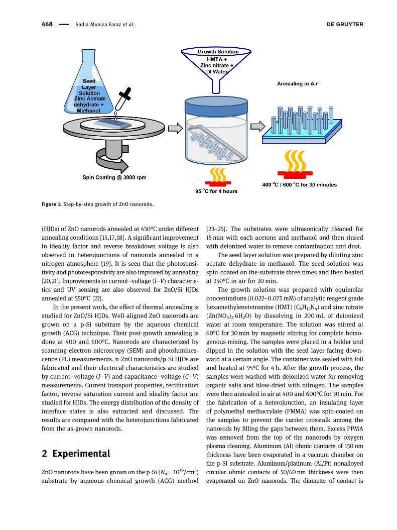
2 Experimental
ZnO nanorods have been grown on the p-Si (Na = 1016/cm3)substrate by aqueous chemical growth (ACG) method
[23–25]. The substrates were ultrasonically cleaned for15 min with each acetone and methanol and then rinsedwith deionized water to remove contamination and dust.
The seed layer solution was prepared by diluting zincacetate dehydrate in methanol. The seed solution wasspin-coated on the substrate three times and then heatedat 250°C in air for 20 min.
The growth solution was prepared with equimolarconcentrations (0.022–0.075mM) of analytic reagent gradehexamethylenetetramine (HMT) (C6H12N4) and zinc nitrate(Zn(NO3)2·6H2O) by dissolving in 200 mL of deionizedwater at room temperature. The solution was stirred at60°C for 30min by magnetic stirring for complete homo-genous mixing. The samples were placed in a holder anddipped in the solution with the seed layer facing down-ward at a certain angle. The container was sealed with foiland heated at 95°C for 4 h. After the growth process, thesamples were washed with deionized water for removingorganic salts and blow-dried with nitrogen. The sampleswere then annealed in air at 400 and 600°C for 30min. Forthe fabrication of a heterojunction, an insulating layerof polymethyl methacrylate (PMMA) was spin-coated onthe samples to prevent the carrier crosstalk among thenanorods by filling the gaps between them. Excess PPMAwas removed from the top of the nanorods by oxygenplasma cleaning. Aluminum (Al) ohmic contacts of 150 nmthickness have been evaporated in a vacuum chamber onthe p-Si substrate. Aluminum/platinum (Al/Pt) nonalloyedcircular ohmic contacts of 50/60 nm thickness were thenevaporated on ZnO nanorods. The diameter of contact is
Figure 1: Step-by-step growth of ZnO nanorods.
468 Sadia Muniza Faraz et al.
0.58mm with specific contact resistance of 1.2 × 10⁻⁵Ω/cm2.A step-by-step growth of ZnO nanorods is shown in Figure 1.
The structural characteristics of ZnO nanorods werestudied by using JEOLJSM – 6301F scanning electron micro-scope (SEM). Photoluminescence (PL) measurements wereperformed at room temperature using laser lines of wave-length 270 or 350 nm from an Ar+ laser as the excitationsource. Keithley SCS-4200 semiconductor characterizationSystem was used for current–voltage (I–V) and capacitan-ce–voltage (C–V)measurements by placing the samples ona probe station.
3 Results and discussion
3.1 SEM
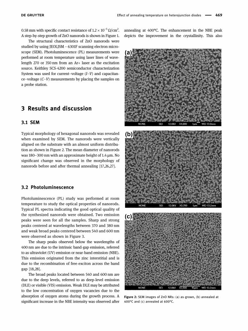
Typical morphology of hexagonal nanorods was revealedwhen examined by SEM. The nanorods were verticallyaligned on the substrate with an almost uniform distribu-tion as shown in Figure 2. The mean diameter of nanorodswas 180–300 nmwith an approximate height of 1.4 μm. Nosignificant change was observed in the morphology ofnanorods before and after thermal annealing [17,26,27].
3.2 Photoluminescence
Photoluminescence (PL) study was performed at roomtemperature to study the optical properties of nanorods.Typical PL spectra indicating the good optical quality ofthe synthesized nanorods were obtained. Two emissionpeaks were seen for all the samples. Sharp and strongpeaks centered at wavelengths between 370 and 380 nmand weak broad peaks centered between 540 and 600 nmwere observed as shown in Figure 3.
The sharp peaks observed below the wavelengths of400 nm are due to the intrinsic band-gap emission, referredto as ultraviolet (UV) emission or near-band emission (NBE).This emission originated from the zinc interstitial and isdue to the recombination of free-exciton across the bandgap [18,28].
The broad peaks located between 540 and 600 nm aredue to the deep levels, referred to as deep-level emission(DLE) or visible (VIS) emission.Weak DLEmay be attributedto the low concentration of oxygen vacancies due to theabsorption of oxygen atoms during the growth process. Asignificant increase in the NBE intensity was observed after
annealing at 400°C. The enhancement in the NBE peakdepicts the improvement in the crystallinity. This also
Figure 2: SEM images of ZnO NRs: (a) as-grown, (b) annealed at400°C and (c) annealed at 600°C.
Effect of annealing temperature on heterojunction diodes 469
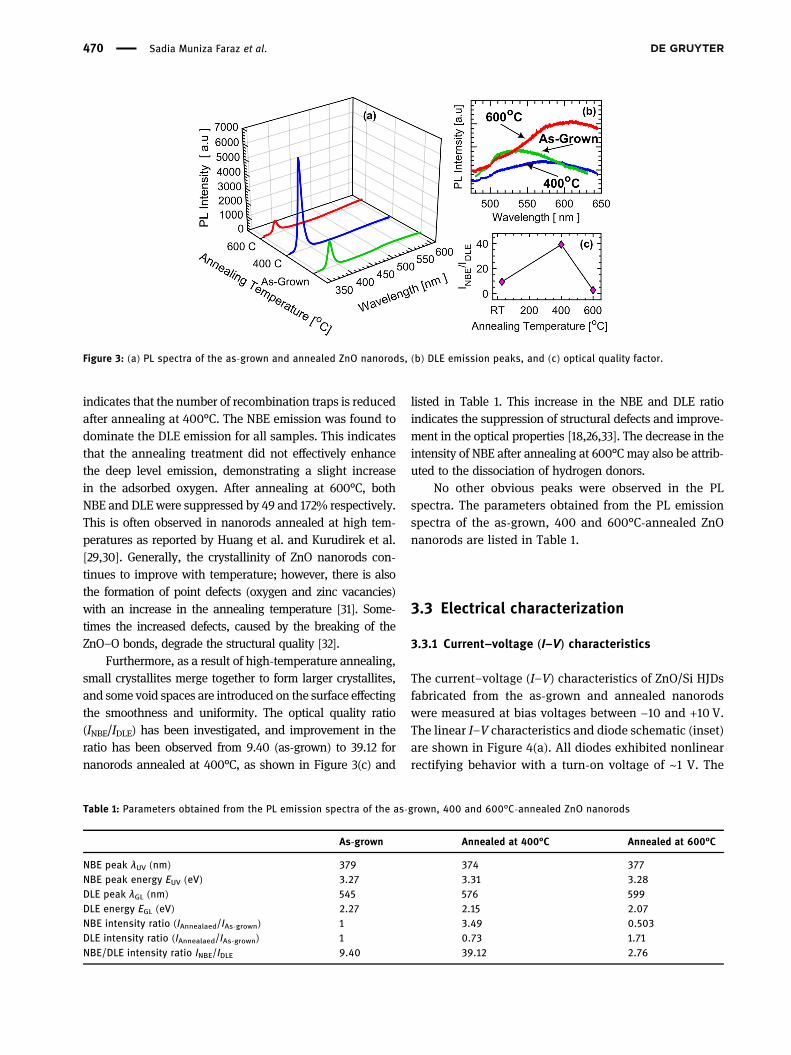
indicates that the number of recombination traps is reducedafter annealing at 400°C. The NBE emission was found todominate the DLE emission for all samples. This indicatesthat the annealing treatment did not effectively enhancethe deep level emission, demonstrating a slight increasein the adsorbed oxygen. After annealing at 600°C, bothNBE and DLE were suppressed by 49 and 172% respectively.This is often observed in nanorods annealed at high tem-peratures as reported by Huang et al. and Kurudirek et al.[29,30]. Generally, the crystallinity of ZnO nanorods con-tinues to improve with temperature; however, there is alsothe formation of point defects (oxygen and zinc vacancies)with an increase in the annealing temperature [31]. Some-times the increased defects, caused by the breaking of theZnO–O bonds, degrade the structural quality [32].
Furthermore, as a result of high-temperature annealing,small crystallites merge together to form larger crystallites,and some void spaces are introduced on the surface effectingthe smoothness and uniformity. The optical quality ratio(INBE/IDLE) has been investigated, and improvement in theratio has been observed from 9.40 (as-grown) to 39.12 fornanorods annealed at 400°C, as shown in Figure 3(c) and
listed in Table 1. This increase in the NBE and DLE ratioindicates the suppression of structural defects and improve-ment in the optical properties [18,26,33]. The decrease in theintensity of NBE after annealing at 600°C may also be attrib-uted to the dissociation of hydrogen donors.
No other obvious peaks were observed in the PLspectra. The parameters obtained from the PL emissionspectra of the as-grown, 400 and 600°C-annealed ZnOnanorods are listed in Table 1.
3.3 Electrical characterization
3.3.1 Current–voltage (I–V) characteristics
The current–voltage (I–V) characteristics of ZnO/Si HJDsfabricated from the as-grown and annealed nanorodswere measured at bias voltages between −10 and +10 V.The linear I–V characteristics and diode schematic (inset)are shown in Figure 4(a). All diodes exhibited nonlinearrectifying behavior with a turn-on voltage of ∼1 V. The
Figure 3: (a) PL spectra of the as-grown and annealed ZnO nanorods, (b) DLE emission peaks, and (c) optical quality factor.
Table 1: Parameters obtained from the PL emission spectra of the as-grown, 400 and 600°C-annealed ZnO nanorods
As-grown Annealed at 400°C Annealed at 600°C
NBE peak λUV (nm) 379 374 377NBE peak energy EUV (eV) 3.27 3.31 3.28DLE peak λGL (nm) 545 576 599DLE energy EGL (eV) 2.27 2.15 2.07NBE intensity ratio (IAnnealaed/IAs-grown) 1 3.49 0.503DLE intensity ratio (IAnnealaed/IAs-grown) 1 0.73 1.71NBE/DLE intensity ratio INBE/IDLE 9.40 39.12 2.76
470 Sadia Muniza Faraz et al.
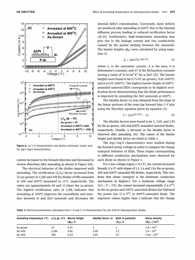
current increased in the forward direction and decreased inreverse directions after annealing as shown in Figure 4(b).
The electrical behavior of the diodes improved withannealing. The rectification (IF/IR) factor increased from23 (as-grown) to 1,596 and 309 for diodes of NRs annealedat 400 and 600°C measured at ±5 V, respectively. Theratios are approximately 69 and 13 times the as-grown.The highest rectification ratio of 1,596 indicates thatannealing at 400°C improves the crystallinity and inter-face between Si and ZnO nanorods and decreases the
internal defect concentration. Conversely, more defectsare produced after annealing at 600°C due to the thermaldiffusion process leading to reduced rectification factor[16,34]. Furthermore, high-temperature annealing maygive rise to the leakage current and low conductivitycaused by the partial melting between the nanorods.The barrier heights (ϕB) were calculated by using equa-tion (1)
=
− /I AA T e⁎ ,qϕ kTo
2 B (1)
where Io is the saturation current, A is the area, k isBoltzmann’s constant, and A* is the Richardson constanthaving a value of 32 A/cm2 K2 for n-ZnO [25]. The barrierheights were found to be 0.75 eV (as-grown), 0.81 (400°C)and 0.63 eV (600°C). The highest barrier height of 400°C-annealed nanorod HJDs corresponds to its highest recti-fication factor demonstrating that the diode performanceis improved by annealing the ZnO nanorods at 400°C.
The ideality factor (n) was obtained from the slope ofthe linear portions of the semi-log forward bias I–V plotusing the Shockley equation given by equation (2):
( )( )= −
/I I e 1 .qV nkTo (2)
The ideality factors were found to be 3, 3.09, and 2.95for the as-grown, 400 and 600°C-annealed nanorod diodes,respectively. Usually, a decrease in the ideality factor isobserved after annealing [35]. The values of the barrierheight and ideality factor are listed in Table 2.
The log I–log V characteristics were studied duringthe forward sweep voltage in order to compare the chargetransport behavior of HJDs. Three slopes correspondingto different conduction mechanisms were observed foreach diode as shown in Figure 5.
For a low-voltage region (<0.5 V), the current increasedlinearly (I α V)with slopes of 1.2, 1.4 and 1 for the as-grown,400 and 600°C-annealed NR diodes, respectively. This con-firms that ohmic transport is the dominant conductionmechanism in Region-I. For a moderate voltage range(0.5 < V < 2V), the current increased exponentially (I α emV)in the as-grown and 400°C-annealed diodes but followedthe power law (I α Vm) in 600°C-annealed diode. Theexponent values higher than 2 indicate that the charge
Figure 4: (a) I–V characteristics and device schematic (inset) and(b) log I–log V characteristics.
Table 2: Electrical parameters calculated from I–V and C–V characteristics for the ZnO/Si heterojunction diodes
Annealing temperature (°C) IF/IR @ ±5 V Barrier height(ϕB), V
Ideality factor (n) Built in potential(Vbi), V
Donor density(Nd), (/cm3)
As-grown 23 0.75 3 1 7.8 × 10¹²
Air-400 1,596 0.81 3.09 1.3 5.9 × 10¹⁵
Air-600 309 0.63 2.95 0.7 7.04 × 10¹⁴
Effect of annealing temperature on heterojunction diodes 471
transport is subjected to the space-charge effect. Infact, the current increased due to increased injection ofaccess carriers after filling the deep traps in the band. Theexponential and power-law dependence of current with
applied voltage shows that the diode behavior is domi-nated by Region-II in all diodes. In Region-III of highervoltages (V > 2 V). log I–log V of all HJDs showed a powerlaw (I α Vm) dependence with a decrease in slope (m ∼ 1.7).At higher voltages, most traps are occupied by injectedcarriers and the accumulation of space charge near theelectrode results in the creation of a field hindering furtherinjection. Hence, the carrier transport approaches the trap-filled limit. This behavior may be attributed to the presenceof oxygen vacancies [36,37].
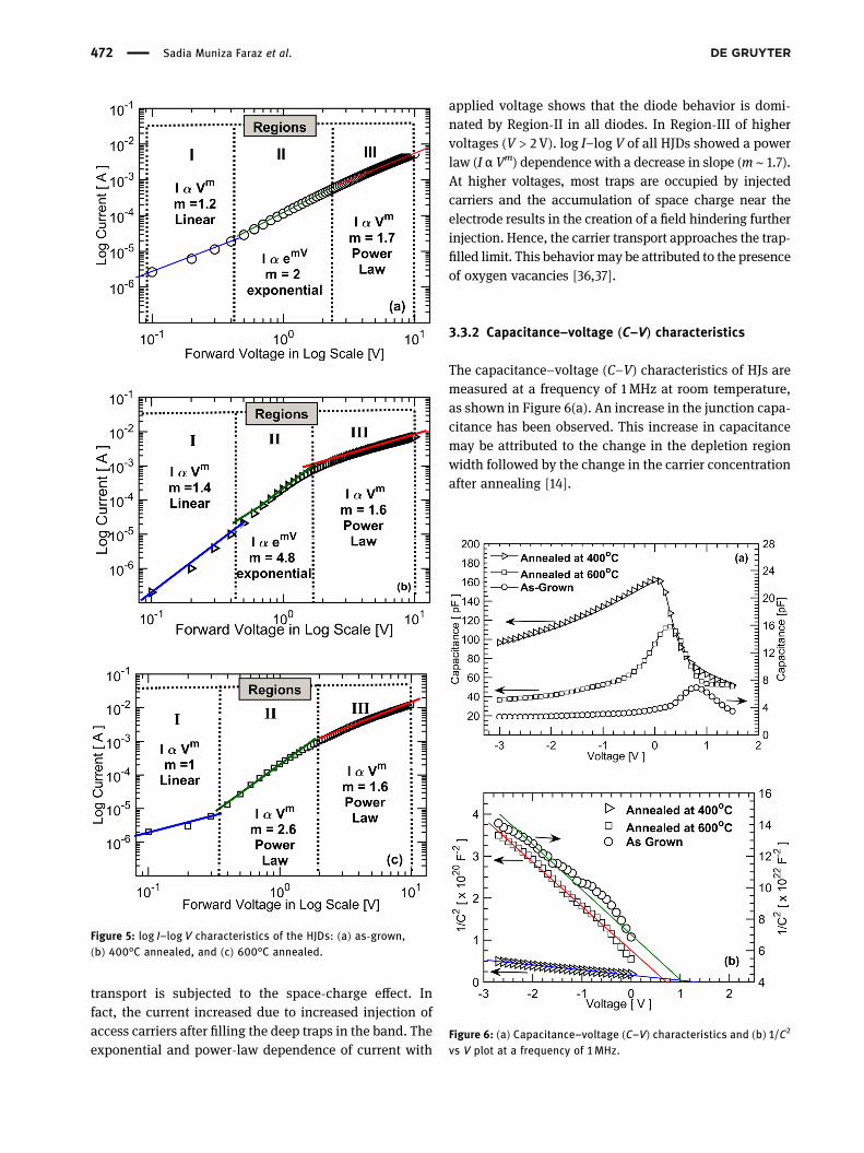
3.3.2 Capacitance–voltage (C–V) characteristics
The capacitance–voltage (C–V) characteristics of HJs aremeasured at a frequency of 1 MHz at room temperature,as shown in Figure 6(a). An increase in the junction capa-citance has been observed. This increase in capacitancemay be attributed to the change in the depletion regionwidth followed by the change in the carrier concentrationafter annealing [14].
Figure 5: log I–log V characteristics of the HJDs: (a) as-grown,(b) 400°C annealed, and (c) 600°C annealed.
Figure 6: (a) Capacitance–voltage (C–V) characteristics and (b) 1/C2vs V plot at a frequency of 1 MHz.
472 Sadia Muniza Faraz et al.

The concentration of electrons (Nd) is obtained byplotting the inverse squared junction capacitance (1/C2)against the applied reverse voltage (V). The concentrationswere extracted from the slope of the linear segment of thecurve as shown in Figure 6(b) by using equation (3):
( )= ×
/
Nqε ε
VA C
2 dd
.dS o
2 2 (3)
Here, εS is the relative permittivity of ZnO having a valueof 8.2. The extracted concentrations are 7.8 × 10¹², 5.9 × 10¹⁵
and 7.04 × 10¹⁴ for the as-grown, 400 and 600°C-annealednanorods diodes, respectively. An increase in the carrierconcentration is observed after annealing and a highercarrier concentration is achieved after annealing at400°C. This increase in carrier concentrations might bedue to the creation of oxygen vacancies and Zn-intersti-tial-related donor-type defects [38]. An increase in theconcentration of hydrogen after annealing might alsobe one of the factors for the increase in the carrier con-centration [39]. The lowest concentration obtained for theas-grownmight be due to the presence of additional oxygenin the form of OH groups due to incomplete reactions ata low growth temperature. These OH groups may act asacceptors giving a low carrier concentration [14,40]. Thebarrier height has been calculated using equation (4):
⎜ ⎟⎛
⎝
⎞
⎠( ) = +
−
ϕ V kTq
NN
ln .C VB biC
d(4)
Here, NC is the effective density of states in the conduc-tion band (CB). Its value is 3.5 × 10¹⁸/cm3 for ZnO,obtained from equation (5):
⎜ ⎟⎛
⎝
⎞
⎠=
/
N πm kTh
2 2 ,nC
⁎
2
3 2(5)
where mn⁎ is the effective mass of electrons given by
=m m0.27n⁎
o. The obtained barrier heights are 1.3 V (as-grown), 1.4 V (400°C) and 0.9 V (600°C) for HJDs. Thebarrier heights obtained from the C–V are comparativelylarger than the barrier heights obtained from the I–Vmeasurements. These discrepancies may be attributedto barrier inhomogeneity, surface defects and image force[25,41]. Second, the interface traps do not respond tohigh-frequency ac signals and hence do not contributeto capacitance [42,43].
3.3.3 Interface states density (NSS)
During the growth of ZnO, an unavoidable SiOx interfa-cial layer is formed at the ZnO/Si interface. This thininterfacial layer is formed due to incomplete covalent
bonds and chemical reactions resulting in a new dielec-tric phase. The electric charge in the thin insulating inter-facial layer introduces a high density of interface states.They affect the diode properties and recombination inthese states is sometimes the main loss mechanism inheterojunctions, especially heterojunction solar cells [14].
These unintentionally introduced interface states aredistributed continuously within the forbidden energygap states and a leakage current is caused by the highdensity of these states. The origin of these states isexactly not known; however, they are introduced due tooxidation of semiconductor surfaces from extended airexposure, surface dipoles, incomplete covalent bonds,hydrogen, chemical reactions during fabrication pro-cesses and sharp discontinuity between semiconductorcrystals [44,45]. The large surface area and small dia-meter of ZnO nanorods are also the reason for these states[46].
The density of interface states (NSS) can be extractedusing I–V and C–V measured values using equation(6) [25]:
⎡
⎣⎢{ ( ) } ⎤
⎦⎥= − −N
qεt
n V εW
1 1 .SSi
i
S
D(6)
Here, WD is the width of the space-charge region, and ɛiand ti are permittivity and thickness of the interfaciallayer. The capacitance of interfacial layer (Ci) is givenby equations (7) and (8);
⎜ ⎟
⎡
⎣⎢
⎛
⎝
⎞
⎠
⎤
⎦⎥
= +C C GωC
1 ,i mama
ma
2(7)
=
CA
ε εt
.i oi
i(8)
Here, ω is angular frequency given by 2πf, and Cma andGma are capacitance and conductance measured at a fre-quency of 1 MHz.The voltage-dependent ideality factorn(V) is extracted from equation (9):
( )
( )
=n V qV
kT ln.
IIo
(9)
Taking into account the voltage-dependent idealityfactor and series resistance, the bias-dependent effectivebarrier height (ϕe) and the energy distribution of interfacestates with respect to the conduction band (EC – ESS) areobtained by using equations (10) and (11), respectively:
⎜ ⎟⎛
⎝ ( )⎞
⎠( )= + − −ϕ φ
n VV IR1 1 ,e bo S (10)
( )− = −E E q ϕ V .c SS e (11)
Effect of annealing temperature on heterojunction diodes 473
The electrical behavior of the diode is affected whenthe electrons excited to the conduction band are trappedby these states. The influence of these interface states ismore pronounced for the compound semiconductor nano-structure as their surfaces have more defects [47].
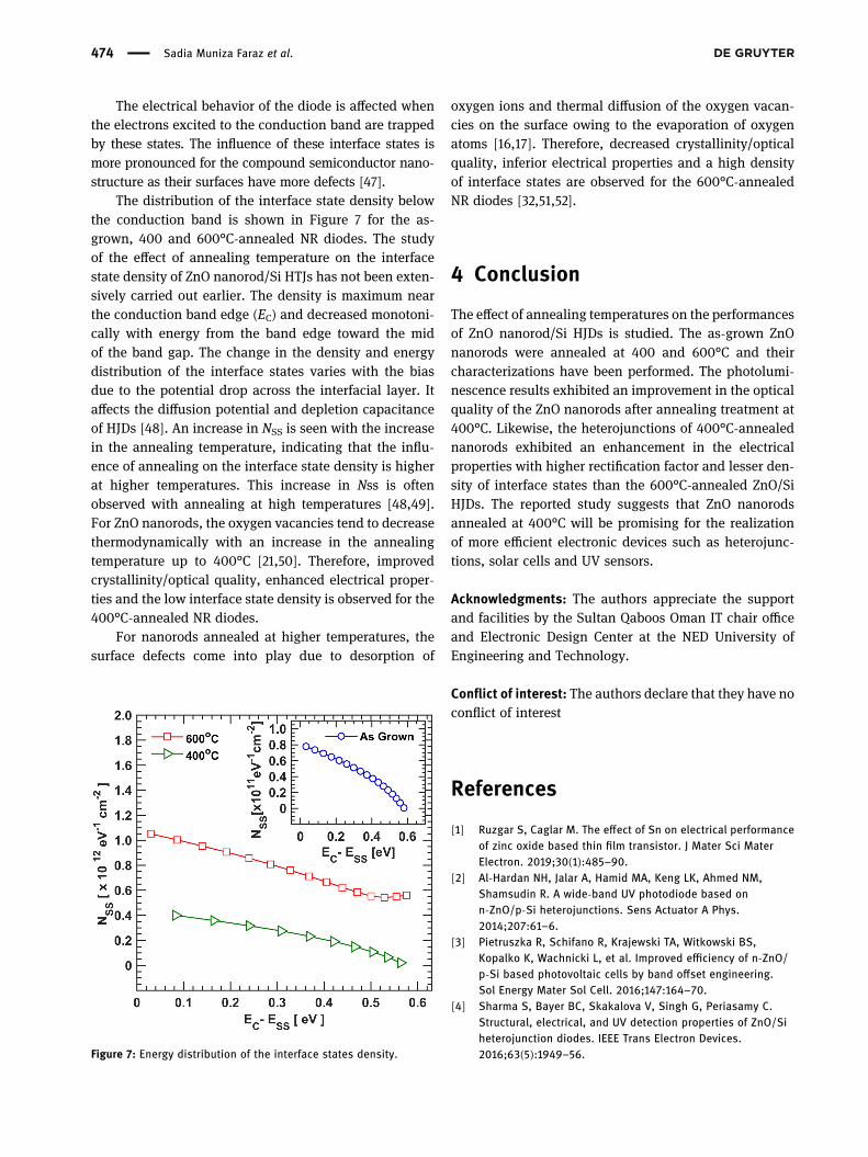
The distribution of the interface state density belowthe conduction band is shown in Figure 7 for the as-grown, 400 and 600°C-annealed NR diodes. The studyof the effect of annealing temperature on the interfacestate density of ZnO nanorod/Si HTJs has not been exten-sively carried out earlier. The density is maximum nearthe conduction band edge (EC) and decreased monotoni-cally with energy from the band edge toward the midof the band gap. The change in the density and energydistribution of the interface states varies with the biasdue to the potential drop across the interfacial layer. Itaffects the diffusion potential and depletion capacitanceof HJDs [48]. An increase in NSS is seen with the increasein the annealing temperature, indicating that the influ-ence of annealing on the interface state density is higherat higher temperatures. This increase in Nss is oftenobserved with annealing at high temperatures [48,49].For ZnO nanorods, the oxygen vacancies tend to decreasethermodynamically with an increase in the annealingtemperature up to 400°C [21,50]. Therefore, improvedcrystallinity/optical quality, enhanced electrical proper-ties and the low interface state density is observed for the400°C-annealed NR diodes.
For nanorods annealed at higher temperatures, thesurface defects come into play due to desorption of
oxygen ions and thermal diffusion of the oxygen vacan-cies on the surface owing to the evaporation of oxygenatoms [16,17]. Therefore, decreased crystallinity/opticalquality, inferior electrical properties and a high densityof interface states are observed for the 600°C-annealedNR diodes [32,51,52].
4 Conclusion
The effect of annealing temperatures on the performancesof ZnO nanorod/Si HJDs is studied. The as-grown ZnOnanorods were annealed at 400 and 600°C and theircharacterizations have been performed. The photolumi-nescence results exhibited an improvement in the opticalquality of the ZnO nanorods after annealing treatment at400°C. Likewise, the heterojunctions of 400°C-annealednanorods exhibited an enhancement in the electricalproperties with higher rectification factor and lesser den-sity of interface states than the 600°C-annealed ZnO/SiHJDs. The reported study suggests that ZnO nanorodsannealed at 400°C will be promising for the realizationof more efficient electronic devices such as heterojunc-tions, solar cells and UV sensors.
Acknowledgments: The authors appreciate the supportand facilities by the Sultan Qaboos Oman IT chair officeand Electronic Design Center at the NED University ofEngineering and Technology.
Conflict of interest: The authors declare that they have noconflict of interest
References
[1] Ruzgar S, Caglar M. The effect of Sn on electrical performanceof zinc oxide based thin film transistor. J Mater Sci MaterElectron. 2019;30(1):485–90.
[2] Al-Hardan NH, Jalar A, Hamid MA, Keng LK, Ahmed NM,Shamsudin R. A wide-band UV photodiode based onn-ZnO/p-Si heterojunctions. Sens Actuator A Phys.2014;207:61–6.
[3] Pietruszka R, Schifano R, Krajewski TA, Witkowski BS,Kopalko K, Wachnicki L, et al. Improved efficiency of n-ZnO/p-Si based photovoltaic cells by band offset engineering.Sol Energy Mater Sol Cell. 2016;147:164–70.
[4] Sharma S, Bayer BC, Skakalova V, Singh G, Periasamy C.Structural, electrical, and UV detection properties of ZnO/Siheterojunction diodes. IEEE Trans Electron Devices.2016;63(5):1949–56.Figure 7: Energy distribution of the interface states density.
474 Sadia Muniza Faraz et al.
[5] Al-Hardan NH, Rashid MM, Aziz AA, Ahmed NM. Low powerconsumption UV sensor based on n-ZnO/p-Si junctions.J Mater Sci Mater Electron. 2019;30(21):19639–46.
[6] Elfadill NG, Hashim MR, Saron KM, Chahrour KM, Qaeed MA,Bououdina M. Ultraviolet–visible photo-response of p-Cu2O/n-ZnO heterojunction prepared on flexible (PET) substrate.Mater Chem Phys. 2015;156:54–60.
[7] Ding M, Zhao D, Yao B, Li Z, Xu X. Ultraviolet photodetectorbased on heterojunction of n-ZnO microwire/p-GaN film.RSC Adv. 2015;5(2):908–12.
[8] Przezdziecka E, Chusnutdinow S, Wierzbicka A, Guziewicz M,Prucnal S, Stachowicz M, et al. Current transport mechanismsin zinc oxide/silicon carbide heterojunction light‐emittingdiodes. Phys Status Solidi (B). 2020;257(9):2000133.
[9] Liu J, Yi F. Fabrication and properties of ZnO nanorods onsilicon nanopillar surface for gas sensor application.J Mater Sci Mater Electron. 2019;30(12):11404–11.
[10] Wei X, Yao R, Jiang Z, Guo T, He F, Wang W, et al. Cirtopic whiteLED with a 490 nm emission peak based on He-Zn annealedZnO nanorods/polymer blend pn heterojunction. J AlloyCompd. 2019;780:306–11.
[11] Ahn H, Wang Y, Jee SH, Park M, Yoon YS, Kim DJ. Enhanced UVactivation of electrochemically doped Ni in ZnO nanorods forroom temperature acetone sensing. Chem Phys Lett.2011;511(4–6):331–5.
[12] Wei S, Lian J, Wu H. Annealing effect on the photolumines-cence properties of ZnO nanorod array prepared by a PLD-assistant wet chemical method. Mater Charact.2010;61(11):1239–44.
[13] Hu SY, Lee YC, Lee JW, Huang JC, Shen JL, Water W. Thestructural and optical properties of ZnO/Si thin films by RTAtreatments. Appl Surf Sci. 2008;254(6):1578–82.
[14] Sahu VK, Misra P, Ajimsha RS, Das AK, Singh B. Effect ofgrowth temperature on diode parameters of n-ZnO/p-Siheterojuction diodes grown by atomic layer deposition.Mater Sci Semicond Process. 2016;54:1–5.
[15] Tu Y, Chen S, Li X, Gorbaciova J, Gillin WP, Krause S, et al.Control of oxygen vacancies in ZnO nanorods by annealing andtheir influence on ZnO/PEDOT: PSS diode behaviour. J MaterChem C. 2018;6(7):1815–21.
[16] Hwang JD, Chen YH. Effects of pre-annealing conditions on thecharacteristics of ZnO nanorods and ZnO/p-Si heterojunctiondiodes grown through hydrothermal method. Thin Solid Films.2012;520(16):5294–9.
[17] Choi JW, Lee CM, Park CH, Lim JH, Park GC, Joo J. Effect ofAnnealing Temperature on Morphology and Electrical Propertyof Hydrothermally-Grown ZnO Nanorods/p-Si HeterojunctionDiodes. J Nanosci Nanotechnol. 2019;19(3):1640–4.
[18] Narayanan GN, Ganesh RS, Karthigeyan A. Effect of annealingtemperature on structural, optical and electrical properties ofhydrothermal assisted zinc oxide nanorods. Thin Solid Films.2016;598:39–45.
[19] Tiagulskyi S, Yatskiv R, Faitová H, Kučerová Š, Roesel D,Vaniš J, et al. Highly rectifying heterojunctions formed byannealed ZnO nanorods on GaN substrates. Nanomaterials.2020;10(3):508.
[20] Gu YZ, Lu HL, Zhang Y, Wang PF, Ding SJ, Zhang DW. Effects ofZnO seed layer annealing temperature on the properties ofn-ZnO NWs/Al 2 O 3/p-Si heterojunction. Opt express.2015;23(19):24456–63.
[21] Khayatian A, Kashi MA, Azimirad R, Safa S, Akhtarian SA. Effectof annealing process in tuning of defects in ZnO nanorods andtheir application in UV photodetectors. Optik.2016;127(11):4675–81.
[22] KAYA Ş. Effect of annealing temperature on structural, elec-trical, and UV sensing characteristics of n-ZnO/p-Si hetero-junction photodiodes. Turkish J Phys. 2019;43(3):252–63.
[23] Faraz SM, Willander M, Wahab Q. Interface state density dis-tribution in Au/n-ZnO nanorods Schottky diodes. In: E-MRS2011 Fall Symposium I (19–23 September 2011, Warszawa,Poland). IOP Conference Series: Materials Science andEngineering. Vol. 34, Issue. 1. IOP Publishing; 2012. p. 012006.
[24] Alnoor H, Pozina G, Khranovskyy V, Liu X, Iandolo D,Willander M, et al. Influence of ZnO seed layer precursor molarratio on the density of interface defects in low temperatureaqueous chemically synthesized ZnO nanorods/GaN light-emitting diodes. J Appl Phys. 2016;119(16):165702.
[25] Faraz SM, Shah W, Alvi NU, Nur O, Wahab QU. Electricalcharacterization of Si/ZnO nanorod PN heterojunction diode.Adv Condens Matter Phys. 2020;2020:1–9.
[26] Lee J, Chung J, Lim S. Improvement of optical properties ofpost-annealed ZnO nanorods. Phys E Low Dimens SystNanostruct. 2010;42(8):2143–6.
[27] Alvi NH, Willander M, Nur O. The effect of the post-growthannealing on the electroluminescence properties of n-ZnOnanorods/p-GaN light emitting diodes. SuperlatticeMicrostruct. 2010;47(6):754–61.
[28] Ahn CH, Kim YY, Kim DC, Mohanta SK, Cho HK. A comparativeanalysis of deep level emission in ZnO layers deposited byvarious methods. J Appl Phys. 2009;105(1):013502.
[29] Huang XH, Tay CB, Zhan ZY, Zhang C, Zheng LX, Venkatesan T,et al. Universal photoluminescence evolution of solution-grown ZnO nanorods with annealing: important role ofhydrogen donor. Cryst Eng Comm. 2011;13(23):7032–6.
[30] Kurudirek SV, Menkara H, Klein BD, Hertel NE, Summers CJ.Effect of annealing temperature on the photoluminescenceand scintillation properties of ZnO nanorods. Nucl InstrumMethods Phys Res Sect. 2018;877:80–6.
[31] Iza DC, Muñoz-Rojas D, Jia Q, Swartzentruber B, MacManus-Driscoll JL. Tuning of defects in ZnO nanorod arrays used inbulk heterojunction solar cells. Nanoscale Res Lett.2012;7(1):1–8.
[32] Bidier SA, Hashim MR, Aldiabat AM. Effect of postannealingtreatment on structural and optical properties of ZnO nanorodsprepared using chemical bath deposition. J Electron Mater.2017;46(7):4455–62.
[33] Ghosh P, Sharma AK. Optical characterization and growthmechanism of combination of zinc oxide nanowires andnanorods at various substrate temperatures. J Nanomater.2013;2013:1–9.
[34] Heo S, Kim C, Lee B, Lee Y, Lee S, Kim DY. Effects of curingtemperature on physical properties of hydrothermally-grownyttrium-doped ZnO nanorods. Curr Appl Phys. 2015;15(5):580–3.
[35] Baydogan N, Karacasu O, Cimenoglu H. Effect of annealingtemperature on ZnO: Al/p-Si heterojunctions. Thin Solid Films.2012;520(17):5790–6.
[36] Zhang J, Yang H, Zhang QL, Dong S, Luo JK. Bipolar resistiveswitching characteristics of low temperature grown ZnO thinfilms by plasma-enhanced atomic layer deposition. Appl PhysLett. 2013;102(1):012113.
Effect of annealing temperature on heterojunction diodes 475
[37] Saha R, Das A, Karmakar A, Chattopadhyay S. Self-rectifyingthreshold resistive switching based non-volatile memory ofCBD/CBD grown vertical n-ZnO nanowire/p-Si heterojunctiondiodes. Adv Mater Proc. 2018;3(4):298–303.
[38] Saha D, Das AK, Ajimsha RS, Misra P, Kukreja LM. Effect ofdisorder on carrier transport in ZnO thin films grown by atomiclayer deposition at different temperatures. J Appl Phys.2013;114(4):043703.
[39] Van de Walle CG. Hydrogen as a cause of doping in zinc oxide.Phys Rev Lett. 2000;85(5):1012.
[40] Huby N, Ferrari S, Guziewicz E, Godlewski M, Osinniy V.Electrical behavior of zinc oxide layers grown by low tem-perature atomic layer deposition. Appl Phys Lett.2008;92(2):023502.
[41] Hussain I, Soomro MY, Bano N, Nur O, Willander M. Interfacetrap characterization and electrical properties of Au-ZnOnanorod Schottky diodes by conductance and capacitancemethods. J Appl Phys. 2012;112(6):064506.
[42] Schroder DK. Semiconductor material and device characteri-zation. 3rd ed. Hoboken, New Jersey: Wiley-IEEE Press, JohnWiley & Sons, Inc.; 2006.
[43] Somvanshi D, Jit S. Analysis of temperature-dependent elec-trical characteristics of n-ZnO nanowires (NWs)/p-Si hetero-junction diodes. IEEE Trans Nanotechnol. 2013;13(1):62–9.
[44] Streetman BG, Banerjee S. Solid state electronic devices.6th ed. Upper Saddle River, NJ: Pearson/Prentice Hall; 2006.
[45] Brillson LJ. Advances in understanding metal-semiconductorinterfaces by surface science techniques. J Phys Chem Solids.1983;44(8):703–33.
[46] Liu X, Wu X, Cao H, Chang RP. Growth mechanism and pro-perties of ZnO nanorods synthesized by plasma-enhancedchemical vapor deposition. J Appl Phys. 2004 Mar15;95(6):3141–7.
[47] Sochacki M, Szmidt J, Bakowski M, Werbowy A. Influence ofannealing on reverse current of 4H–SiC Schottky diodes.Diam Relat Mater. 2002 Mar 1;11(3–6):1263–7.
[48] Reddy YM, Padmasuvarna R, Narasappa TL, Sreehith P,Padma R, Rao LD, et al. Effect of annealing temperature on theelectrical, structural and surface morphological properties ofRu/Ti Schottky contacts on n-type InP. SuperlatticeMicrostruct. 2015;86:280–91.
[49] Saha AR, Chattopadhyay S, Dalapati GK, Bose C, Maiti CK.Effect of annealing on interface state density of Ni-silicided/Si1−xGex Schottky diode. Mater Sci Semicond Process.2005;8(1–3):249–53.
[50] Kaya S, Yilmaz E. Effects of interfacial layer on the electricalproperties of n-ZnO/p-Si heterojunction diodes between260 and 340 K. J Mater Sci Mater Electron.2019;30(13):12170–9.
[51] Aydoğan Ş, Grilli ML, Yilmaz M, Çaldiran Z, Kaçuş H. A facilegrowth of spray based ZnO films and device performanceinvestigation for Schottky diodes: determination ofinterface state density distribution. J Alloy Compd.2017;708:55–66.
[52] Ejderha K, Orak I, Duman S, Turut A. The effect of thermalannealing and measurement temperature on interface statedensity distribution and time constant in Ni/n-GaP rectifyingcontacts. J Electron Mater. 2018;47(7):3502–9.
476 Sadia Muniza Faraz et al.


![SICregang - Willkommen - Sysmex Austria · Positive Diff. Morph. Count WBC & 27.76 IOA3/uL 1 OA6/uL g/dL] % pgg 1 OA3/uL] fL 113/uL 0/0 0/0 IOA3/uL IOA3/uL 1 OA3/uL IOA3/uL IOA3/uL](https://img.pdfslide.tips/doc/110x75/5ac49e847f8b9a2b5c8d1e67/sicregang-willkommen-sysmex-austria-diff-morph-count-wbc-2776-ioa3ul-1-oa6ul.jpg)