Embed Size (px)
Citation preview
NEWS 2012 APR
No. 415
4
- I/O-oriented High-performance Computing in the Big-data Era -
05
01
Intelligent Sensors ofArtificial DNA NanostructuresMiki Hirabayashi
03
R&D Information Infrastructure forGathering and Storing Large-scale Data
07 nano tech 2012 Report on 11th InternationalNanotechnology Exhibition/Technology Conference
08
11
Report on 6th NICT/EMC-net Technical Forum
10
July 1st of this year will be 1 second longer
Report on CRYPTREC Symposium 2012
09 Report on Entrepreneurs Koshien for youngergenerations and 2011 Information andCommunications Venture Business Plan Contest
Hiroshi Ishijima
Michiaki Iwazume
- Behind the scenes of primary frequency standards development -
For reliable ticking
Solid, reliable technology that expedites research activitiesPrototype Development Part 3
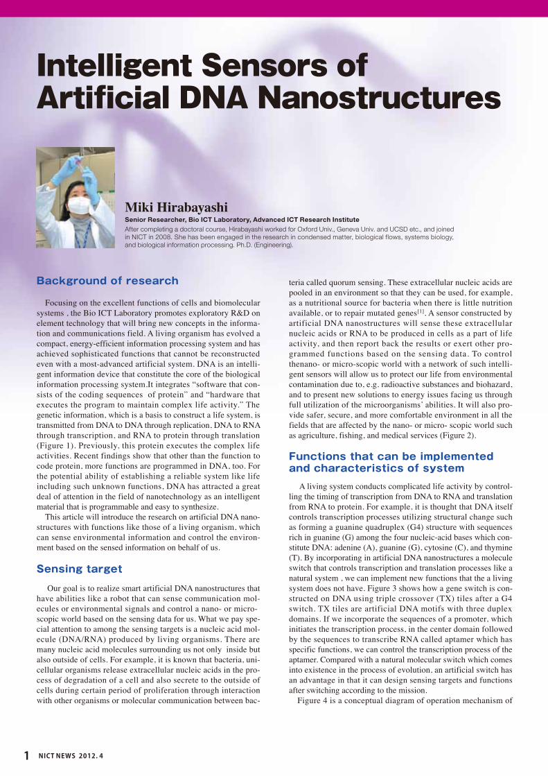
Focusing on the excellent functions of cells and biomolecular systems , the Bio ICT Laboratory promotes exploratory R&D on element technology that will bring new concepts in the informa-tion and communications field. A living organism has evolved a compact, energy-efficient information processing system and has achieved sophisticated functions that cannot be reconstructed even with a most-advanced artificial system. DNA is an intelli-gent information device that constitute the core of the biological information processing system.It integrates “software that con-sists of the coding sequences of protein” and “hardware that executes the program to maintain complex life activity.” The genetic information, which is a basis to construct a life system, is transmitted from DNA to DNA through replication, DNA to RNA through transcription, and RNA to protein through translation (Figure 1). Previously, this protein executes the complex life activities. Recent findings show that other than the function to code protein, more functions are programmed in DNA, too. For the potential ability of establishing a reliable system like life including such unknown functions, DNA has attracted a great deal of attention in the field of nanotechnology as an intelligent material that is programmable and easy to synthesize.
This article will introduce the research on artificial DNA nano-structures with functions like those of a living organism, which can sense environmental information and control the environ-ment based on the sensed information on behalf of us.
Our goal is to realize smart artificial DNA nanostructures that have abilities like a robot that can sense communication mol-ecules or environmental signals and control a nano- or micro-scopic world based on the sensing data for us. What we pay spe-cial attention to among the sensing targets is a nucleic acid mol-ecule (DNA/RNA) produced by living organisms. There are many nucleic acid molecules surrounding us not only inside but also outside of cells. For example, it is known that bacteria, uni-cellular organisms release extracellular nucleic acids in the pro-cess of degradation of a cell and also secrete to the outside of cells during certain period of proliferation through interaction with other organisms or molecular communication between bac-
teria called quorum sensing. These extracellular nucleic acids are pooled in an environment so that they can be used, for example, as a nutritional source for bacteria when there is little nutrition available, or to repair mutated genes[1]. A sensor constructed by artificial DNA nanostructures will sense these extracellular nucleic acids or RNA to be produced in cells as a part of life activity, and then report back the results or exert other pro-grammed functions based on the sensing data. To control thenano- or micro-scopic world with a network of such intelli-gent sensors will allow us to protect our life from environmental contamination due to, e.g. radioactive substances and biohazard, and to present new solutions to energy issues facing us through full utilization of the microorganisms’ abilities. It will also pro-vide safer, secure, and more comfortable environment in all the fields that are affected by the nano- or micro- scopic world such as agriculture, fishing, and medical services (Figure 2).
A living system conducts complicated life activity by control-ling the timing of transcription from DNA to RNA and translation from RNA to protein. For example, it is thought that DNA itself controls transcription processes utilizing structural change such as forming a guanine quadruplex (G4) structure with sequences rich in guanine (G) among the four nucleic-acid bases which con-stitute DNA: adenine (A), guanine (G), cytosine (C), and thymine (T). By incorporating in artificial DNA nanostructures a molecule switch that controls transcription and translation processes like a natural system , we can implement new functions that the a living system does not have. Figure 3 shows how a gene switch is con-structed on DNA using triple crossover (TX) tiles after a G4 switch. TX tiles are artificial DNA motifs with three duplex domains. If we incorporate the sequences of a promoter, which initiates the transcription process, in the center domain followed by the sequences to transcribe RNA called aptamer which has specific functions, we can control the transcription process of the aptamer. Compared with a natural molecular switch which comes into existence in the process of evolution, an artificial switch has an advantage in that it can design sensing targets and functions after switching according to the mission.
Figure 4 is a conceptual diagram of operation mechanism of
Background of research
Sensing target
Functions that can be implemented and characteristics of system
Intelligent Sensors ofArtificial DNA Nanostructures
After completing a doctoral course, Hirabayashi worked for Oxford Univ., Geneva Univ. and UCSD etc., and joined in NICT in 2008. She has been engaged in the research in condensed matter, biological flows, systems biology, and biological information processing. Ph.D. (Engineering).
Miki HirabayashiSenior Researcher, Bio ICT Laboratory, Advanced ICT Research Institute
NICT NEWS 2012. 4 1
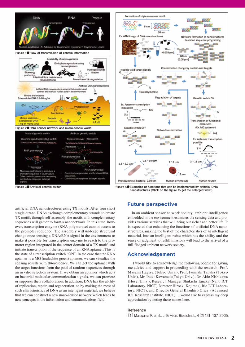
artificial DNA nanostructures using TX motifs. After four short single-strand DNAs exchange complementary strands to create TX motifs through self-assembly, the motifs with complementary sequences will gather to form a nanonetwork. In this state, how-ever, transcription enzyme (RNA polymerase) cannot access to the promoter sequence. The assembly will undergo structural change once sensing a DNA/RNA signal in the environment to make it possible for transcription enzyme to reach to the pro-moter region integrated in the center domain of a TX motif, and initiate transcription of the sequence of an RNA aptamer. This is the state of a transcription switch “ON”. In the case that the RNA aptamer is a MG (malachite green) aptamer, we can visualize the sensing results with fluorescence. We can get the aptamer with the target functions from the pool of random sequences through an in vitro selection system. If we obtain an aptamer which acts on bacterial molecular communication signals, we can promote or suppress their collaboration. In addition, DNA has the ability of replication, repair, and regeneration, so by making the most of such characteristics of DNA as an intelligent material, we believe that we can construct a new nano-sensor network which leads to new concepts in the information and communications field.
In an ambient sensor network society, ambient intelligence embedded in the environment estimates the sensing data and pro-vides various services that will bring our richer and better life. It is expected that enhancing the functions of artificial DNA nano-structures, making the best of the characteristics of an intelligent material, into an intelligent robot which has the ability and the sense of judgment to fulfill missions will lead to the arrival of a full-fledged ambient network society.
I would like to acknowledge the following people for giving me advice and support in proceeding with the research: Prof. Masami Hagiya (Tokyo Univ.), Prof. Fumiaki Tanaka (Tokyo Univ.), Mr. Ibuki Kawamata(Tokyo Univ.), Dr. Akio Nishikawa (Hosei Univ.), Research Manager Shukichi Tanaka (Nano ICT Laboratory, NICT) Director Hiroaki Kojima (, Bio ICT Labora-tory, NICT), and Director General Kazuhiro Oiwa (Advanced ICT Research Institute, NICT). I would like to express my deep appreciation by noting these names here.
Future perspective
Acknowledgement
Figure 4●Examples of functions that can be implemented by artificial DNA nanostructures (Click on the figure to get the enlarged view.)
Figure 3●Artificial genetic switch
Figure 2●DNA sensor network and micro-scopic world
Figure 1●Flow of transmission of genetic information
Reference[1]Maruyama F. et al., J. Environ. Biotechnol., 4(2)131‒137, 2005.
NICT NEWS 2012. 4 2
These days, a flood of non-programmed data is being created in real time from lifelogs, sensors, and automobiles that are con-nected to networks called “Internet of Things”, and all kinds. These data can quickly accumulate to volumes exceeding a petabyte, with entries numbering in the hundreds of millions to tens of billions, which is why this data is called “big data.” How to gather and effectively utilize this big data was discussed in the Davos Forum*1 that was held in January 2012, which indicates the mounting expectations and concern in big data as the frontier of new global business services and innovations, not only from those in the ICT field, but also those in business communities.
The Universal Communication Research Institute researches and develops fudamental technologies, such as information analysis technology, based on multi-lingual spoken language technologies and advanced semantic processing with the goal of realization of universal communications. These technologies require collecting vast amounts of text data and developing a massive corpus*2 and various language resources*3. Our R&D theme is to establish fundamental information technology to effi-ciently collect, store, and quickly retrieve a huge amount of spe-cific information on the internet. We are conducting an empirical study on (1) high-performance web crawling technology, (2) large-scale distributed data storage, and (3) development and management technology for large-scale computer infrastructure.
A web crawler is a type of software that automatically collects information on the network. Its execution principle is very simple: sequentially visiting the links embedded in web docu-ments. The Internet, however, contains many spam pages and duplicate sites. Some information is rarely updated, while other information, such as news, is frequently updated. It is also essen-tial to ensure that the network environment and business partner websites are not overloaded.
The laboratory developed and operated a web crawler as an information base for the web information analyzing system WISDOM developed under the Second Medium-term Plan (FY 2006 to 2010). The crawler collects up to about 10 million web pages a day and it has accumulated about 1 billion web pages.
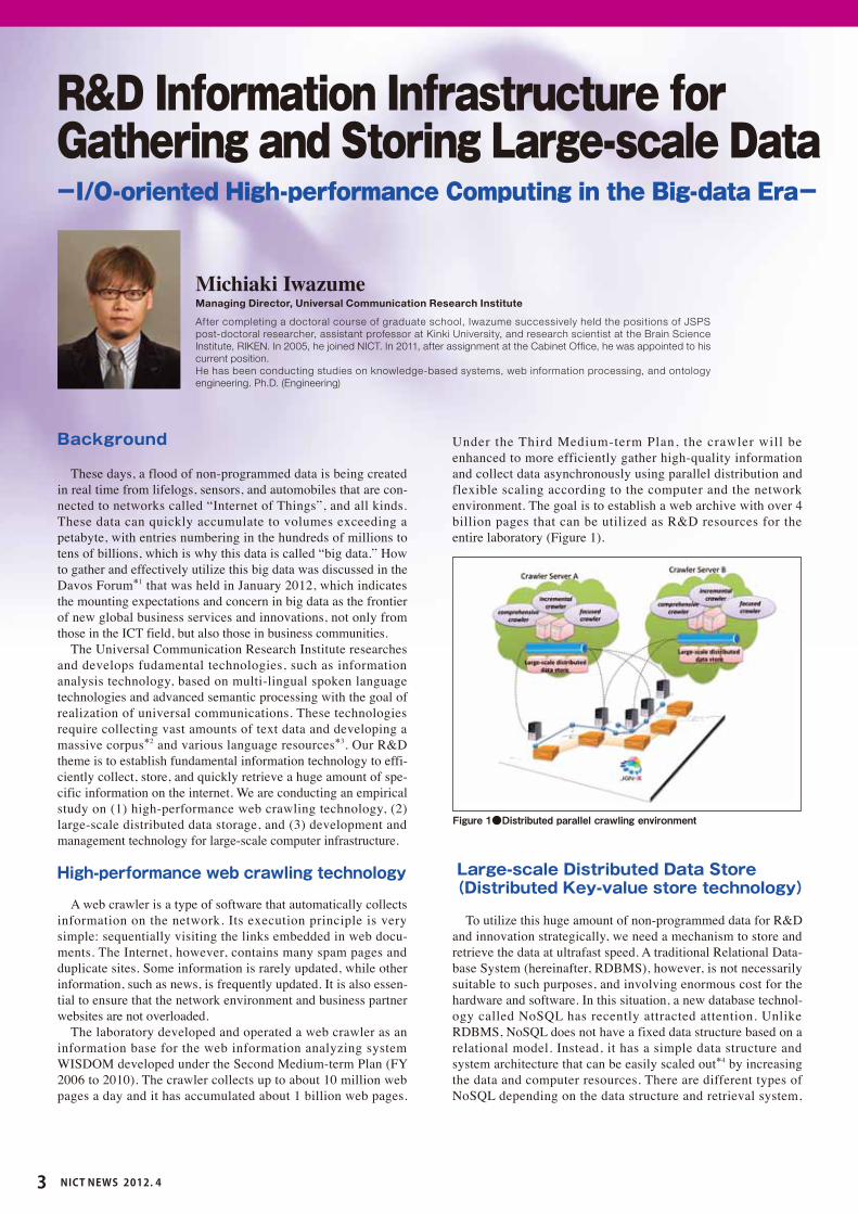
Under the Third Medium-term Plan, the crawler will be enhanced to more efficiently gather high-quality information and collect data asynchronously using parallel distribution and flexible scaling according to the computer and the network environment. The goal is to establish a web archive with over 4 billion pages that can be utilized as R&D resources for the entire laboratory (Figure 1).
To utilize this huge amount of non-programmed data for R&D and innovation strategically, we need a mechanism to store and retrieve the data at ultrafast speed. A traditional Relational Data-base System (hereinafter, RDBMS), however, is not necessarily suitable to such purposes, and involving enormous cost for the hardware and software. In this situation, a new database technol-ogy called NoSQL has recently attracted attention. Unlike RDBMS, NoSQL does not have a fixed data structure based on a relational model. Instead, it has a simple data structure and system architecture that can be easily scaled out*4 by increasing the data and computer resources. There are different types of NoSQL depending on the data structure and retrieval system,
Background
High-performance web crawling technology Large-scale Distributed Data Store (Distributed Key-value store technology)
R&D Information Infrastructure for Gathering and Storing Large-scale Data -I/O-oriented High-performance Computing in the Big-data Era-
Figure 1●Distributed parallel crawling environment
After completing a doctoral course of graduate school, Iwazume successively held the positions of JSPS post-doctoral researcher, assistant professor at Kinki University, and research scientist at the Brain Science Institute, RIKEN. In 2005, he joined NICT. In 2011, after assignment at the Cabinet Office, he was appointed to his current position.He has been conducting studies on knowledge-based systems, web information processing, and ontology engineering. Ph.D. (Engineering)
Michiaki IwazumeManaging Director, Universal Communication Research Institute
NICT NEWS 2012. 4 3
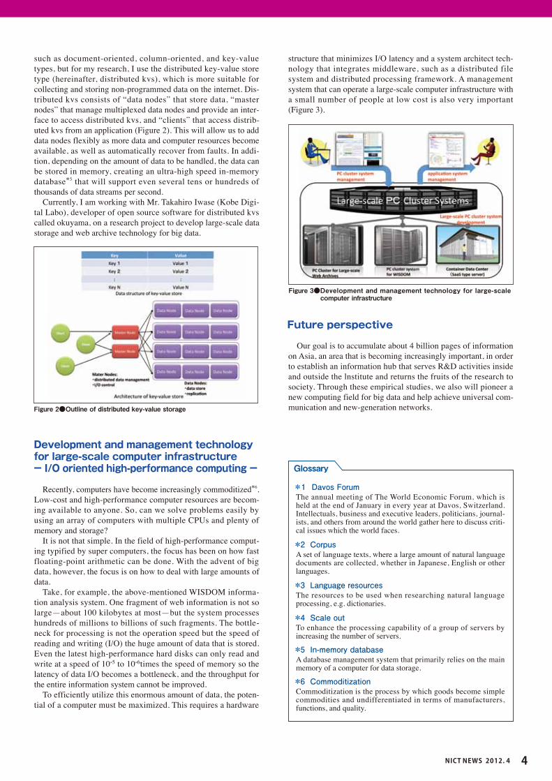
such as document-oriented, column-oriented, and key-value types, but for my research, I use the distributed key-value store type (hereinafter, distributed kvs), which is more suitable for collecting and storing non-programmed data on the internet. Dis-tributed kvs consists of “data nodes” that store data, “master nodes” that manage multiplexed data nodes and provide an inter-face to access distributed kvs, and “clients” that access distrib-uted kvs from an application (Figure 2). This will allow us to add data nodes flexibly as more data and computer resources become available, as well as automatically recover from faults. In addi-tion, depending on the amount of data to be handled, the data can be stored in memory, creating an ultra-high speed in-memory database*5 that will support even several tens or hundreds of thousands of data streams per second.
Currently, I am working with Mr. Takahiro Iwase (Kobe Digi-tal Labo), developer of open source software for distributed kvs called okuyama, on a research project to develop large-scale data storage and web archive technology for big data.
Recently, computers have become increasingly commoditized*6.
Low-cost and high-performance computer resources are becom-ing available to anyone. So, can we solve problems easily by using an array of computers with multiple CPUs and plenty of memory and storage?
It is not that simple. In the field of high-performance comput-ing typified by super computers, the focus has been on how fast floating-point arithmetic can be done. With the advent of big data, however, the focus is on how to deal with large amounts of data.
Take, for example, the above-mentioned WISDOM informa-tion analysis system. One fragment of web information is not so large—about 100 kilobytes at most—but the system processes hundreds of millions to billions of such fragments. The bottle-neck for processing is not the operation speed but the speed of reading and writing (I/O) the huge amount of data that is stored. Even the latest high-performance hard disks can only read and write at a speed of 10-5 to 10-6times the speed of memory so the latency of data I/O becomes a bottleneck, and the throughput for the entire information system cannot be improved.
To efficiently utilize this enormous amount of data, the poten-tial of a computer must be maximized. This requires a hardware
structure that minimizes I/O latency and a system architect tech-nology that integrates middleware, such as a distributed file system and distributed processing framework. A management system that can operate a large-scale computer infrastructure with a small number of people at low cost is also very important (Figure 3).
Our goal is to accumulate about 4 billion pages of information
on Asia, an area that is becoming increasingly important, in order to establish an information hub that serves R&D activities inside and outside the lnstitute and returns the fruits of the research to society. Through these empirical studies, we also will pioneer a new computing field for big data and help achieve universal com-munication and new-generation networks.
Glossary
The annual meeting of The World Economic Forum, which is held at the end of January in every year at Davos, Switzerland. Intellectuals, business and executive leaders, politicians, journal-ists, and others from around the world gather here to discuss criti-cal issues which the world faces.
*1 Davos Forum
A set of language texts, where a large amount of natural language documents are collected, whether in Japanese, English or other languages.
*2 Corpus
The resources to be used when researching natural language processing, e.g. dictionaries.
*3 Language resources
To enhance the processing capability of a group of servers by increasing the number of servers.
*4 Scale out
A database management system that primarily relies on the main memory of a computer for data storage.
*5 In-memory database
Commoditization is the process by which goods become simple commodities and undifferentiated in terms of manufacturers, functions, and quality.
*6 Commoditization
Development and management technologyfor large-scale computer infrastructure- I/O oriented high-performance computing -
Future perspective
Figure 2●Outline of distributed key-value storage
Figure 3●Development and management technology for large-scale computer infrastructure
NICT NEWS 2012. 4 4
The Atomic Frequency Standards Group, Space-Time Standards Laboratory, to which I belong, develops frequency standards and their related technologies. Specifically, the development includes NICT-CsF1 and CsF2, which are the primary frequency standards*2 based on cesium atomic fountain*3, as well as the strontium optical lattice clock*4 and the calcium ion clock*5, which are intended to be next-generation standards. Development also includes optical frequency combs*6 for measuring frequencies in the optical range. With these efforts, we maintain the accuracy of the SI second*7 and enhance the accuracy of world time standards, such as TAI (international atomic time).
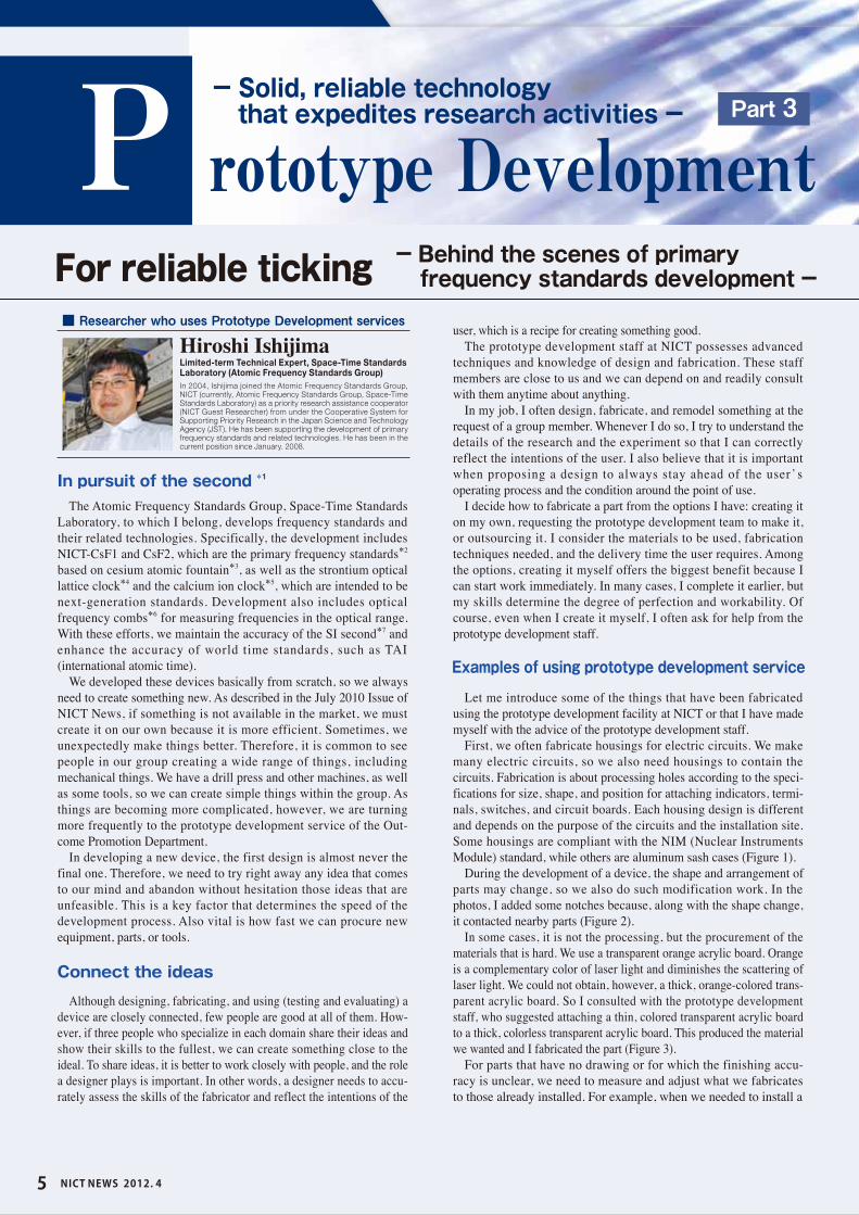
We developed these devices basically from scratch, so we always need to create something new. As described in the July 2010 Issue of NICT News, if something is not available in the market, we must create it on our own because it is more efficient. Sometimes, we unexpectedly make things better. Therefore, it is common to see people in our group creating a wide range of things, including mechanical things. We have a drill press and other machines, as well as some tools, so we can create simple things within the group. As things are becoming more complicated, however, we are turning more frequently to the prototype development service of the Out-come Promotion Department.
In developing a new device, the first design is almost never the final one. Therefore, we need to try right away any idea that comes to our mind and abandon without hesitation those ideas that are unfeasible. This is a key factor that determines the speed of the development process. Also vital is how fast we can procure new equipment, parts, or tools.
Although designing, fabricating, and using (testing and evaluating) a device are closely connected, few people are good at all of them. How-ever, if three people who specialize in each domain share their ideas and show their skills to the fullest, we can create something close to the ideal. To share ideas, it is better to work closely with people, and the role a designer plays is important. In other words, a designer needs to accu-rately assess the skills of the fabricator and reflect the intentions of the
user, which is a recipe for creating something good.The prototype development staff at NICT possesses advanced
techniques and knowledge of design and fabrication. These staff members are close to us and we can depend on and readily consult with them anytime about anything.
In my job, I often design, fabricate, and remodel something at the request of a group member. Whenever I do so, I try to understand the details of the research and the experiment so that I can correctly reflect the intentions of the user. I also believe that it is important when proposing a design to always stay ahead of the user’ s operating process and the condition around the point of use.
I decide how to fabricate a part from the options I have: creating it on my own, requesting the prototype development team to make it, or outsourcing it. I consider the materials to be used, fabrication techniques needed, and the delivery time the user requires. Among the options, creating it myself offers the biggest benefit because I can start work immediately. In many cases, I complete it earlier, but my skills determine the degree of perfection and workability. Of course, even when I create it myself, I often ask for help from the prototype development staff.
Let me introduce some of the things that have been fabricated using the prototype development facility at NICT or that I have made myself with the advice of the prototype development staff.
First, we often fabricate housings for electric circuits. We make many electric circuits, so we also need housings to contain the circuits. Fabrication is about processing holes according to the speci-fications for size, shape, and position for attaching indicators, termi-nals, switches, and circuit boards. Each housing design is different and depends on the purpose of the circuits and the installation site. Some housings are compliant with the NIM (Nuclear Instruments Module) standard, while others are aluminum sash cases (Figure 1).
During the development of a device, the shape and arrangement of parts may change, so we also do such modification work. In the photos, I added some notches because, along with the shape change, it contacted nearby parts (Figure 2).
In some cases, it is not the processing, but the procurement of the materials that is hard. We use a transparent orange acrylic board. Orange is a complementary color of laser light and diminishes the scattering of laser light. We could not obtain, however, a thick, orange-colored trans-parent acrylic board. So I consulted with the prototype development staff, who suggested attaching a thin, colored transparent acrylic board to a thick, colorless transparent acrylic board. This produced the material we wanted and I fabricated the part (Figure 3).
For parts that have no drawing or for which the finishing accu-racy is unclear, we need to measure and adjust what we fabricates to those already installed. For example, when we needed to install a
In pursuit of the second *1
Connect the ideas
Examples of using prototype development service
■ Researcher who uses Prototype Development services
P rototype Development - Solid, reliable technology that expedites research activities - Part 3
- Behind the scenes of primary frequency standards development - For reliable ticking
Hiroshi IshijimaLimited-term Technical Expert, Space-Time StandardsLaboratory (Atomic Frequency Standards Group)In 2004, Ishijima joined the Atomic Frequency Standards Group, NICT (currently, Atomic Frequency Standards Group, Space-Time Standards Laboratory) as a priority research assistance cooperator (NICT Guest Researcher) from under the Cooperative System for Supporting Priority Research in the Japan Science and Technology Agency (JST). He has been supporting the development of primary frequency standards and related technologies. He has been in the current position since January. 2008.
NICT NEWS 2012. 4 5
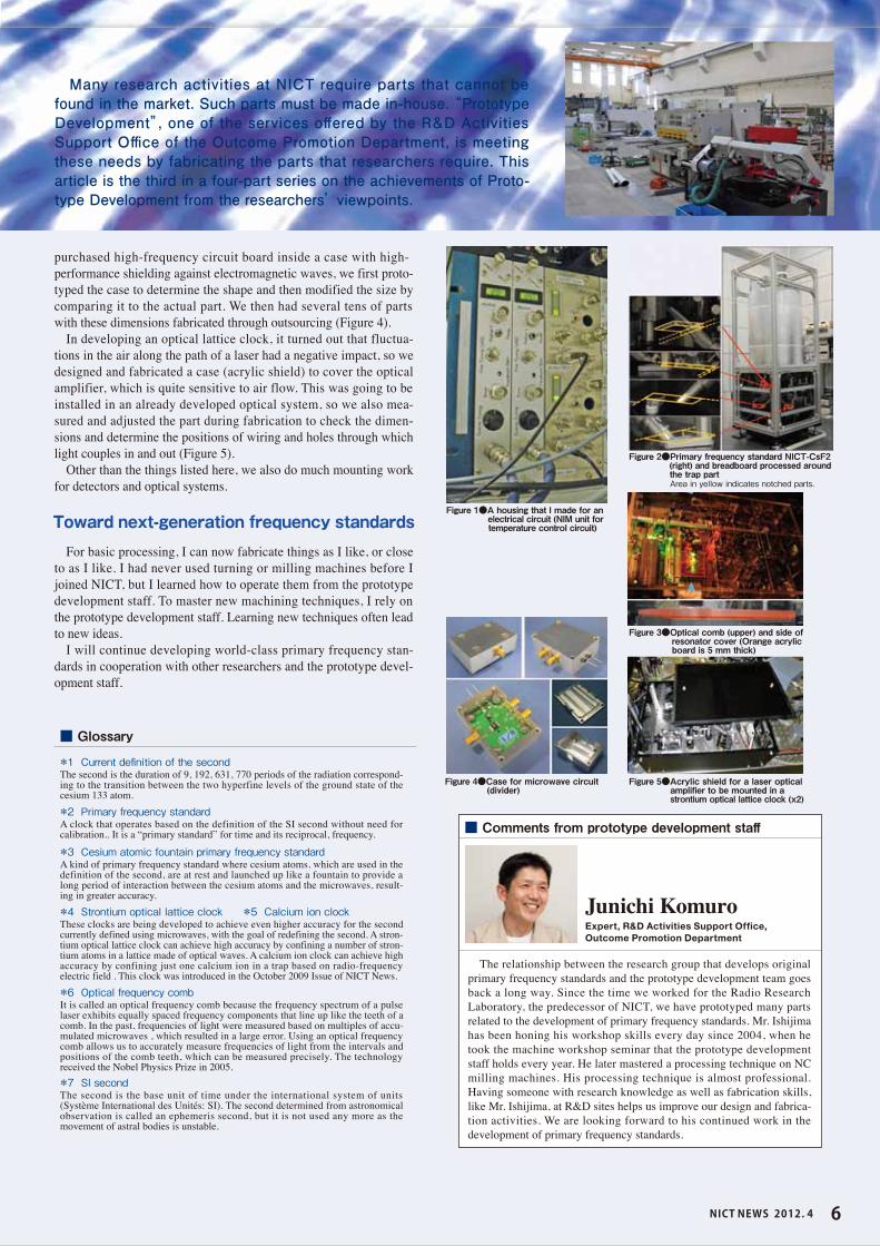
purchased high-frequency circuit board inside a case with high-performance shielding against electromagnetic waves, we first proto-typed the case to determine the shape and then modified the size by comparing it to the actual part. We then had several tens of parts with these dimensions fabricated through outsourcing (Figure 4).
In developing an optical lattice clock, it turned out that fluctua-tions in the air along the path of a laser had a negative impact, so we designed and fabricated a case (acrylic shield) to cover the optical amplifier, which is quite sensitive to air flow. This was going to be installed in an already developed optical system, so we also mea-sured and adjusted the part during fabrication to check the dimen-sions and determine the positions of wiring and holes through which light couples in and out (Figure 5).
Other than the things listed here, we also do much mounting work for detectors and optical systems.
For basic processing, I can now fabricate things as I like, or close
to as I like. I had never used turning or milling machines before I joined NICT, but I learned how to operate them from the prototype development staff. To master new machining techniques, I rely on the prototype development staff. Learning new techniques often lead to new ideas.
I will continue developing world-class primary frequency stan-dards in cooperation with other researchers and the prototype devel-opment staff.
Toward next-generation frequency standards
■ Comments from prototype development staff
■ Glossary
The relationship between the research group that develops original primary frequency standards and the prototype development team goes back a long way. Since the time we worked for the Radio Research Laboratory, the predecessor of NICT, we have prototyped many parts related to the development of primary frequency standards. Mr. Ishijima has been honing his workshop skills every day since 2004, when he took the machine workshop seminar that the prototype development staff holds every year. He later mastered a processing technique on NC milling machines. His processing technique is almost professional. Having someone with research knowledge as well as fabrication skills, like Mr. Ishijima, at R&D sites helps us improve our design and fabrica-tion activities. We are looking forward to his continued work in the development of primary frequency standards.
Area in yellow indicates notched parts.
The second is the duration of 9, 192, 631, 770 periods of the radiation correspond-ing to the transition between the two hyperfine levels of the ground state of the cesium 133 atom.
*1 Current definition of the second
A clock that operates based on the definition of the SI second without need for calibration.. It is a “primary standard” for time and its reciprocal, frequency.
*2 Primary frequency standard
A kind of primary frequency standard where cesium atoms, which are used in the definition of the second, are at rest and launched up like a fountain to provide a long period of interaction between the cesium atoms and the microwaves, result-ing in greater accuracy.
*3 Cesium atomic fountain primary frequency standard
It is called an optical frequency comb because the frequency spectrum of a pulse laser exhibits equally spaced frequency components that line up like the teeth of a comb. In the past, frequencies of light were measured based on multiples of accu-mulated microwaves , which resulted in a large error. Using an optical frequency comb allows us to accurately measure frequencies of light from the intervals and positions of the comb teeth, which can be measured precisely. The technology received the Nobel Physics Prize in 2005.
*6 Optical frequency comb
The second is the base unit of time under the international system of units (Système International des Unités: SI). The second determined from astronomical observation is called an ephemeris second, but it is not used any more as the movement of astral bodies is unstable.
*7 SI second
These clocks are being developed to achieve even higher accuracy for the second currently defined using microwaves, with the goal of redefining the second. A stron-tium optical lattice clock can achieve high accuracy by confining a number of stron-tium atoms in a lattice made of optical waves. A calcium ion clock can achieve high accuracy by confining just one calcium ion in a trap based on radio-frequency electric field . This clock was introduced in the October 2009 Issue of NICT News.
*4 Strontium optical lattice clock *5 Calcium ion clock Junichi KomuroExpert, R&D Activities Support Office, Outcome Promotion Department
Figure 1●A housing that I made for an electrical circuit (NIM unit for temperature control circuit)
Figure 2●Primary frequency standard NICT-CsF2 (right) and breadboard processed around the trap part
Figure 3●Optical comb (upper) and side of resonator cover (Orange acrylic board is 5 mm thick)
Figure 5●Acrylic shield for a laser optical amplifier to be mounted in a strontium optical lattice clock (x2)
Figure 4●Case for microwave circuit (divider)
Many research activities at NICT require parts that cannot be found in the market. Such parts must be made in-house. “Prototype Development”, one of the services offered by the R&D Activities Support Office of the Outcome Promotion Department, is meeting these needs by fabricating the parts that researchers require. This article is the third in a four-part series on the achievements of Proto-type Development from the researchers’ viewpoints.
NICT NEWS 2012. 4 6
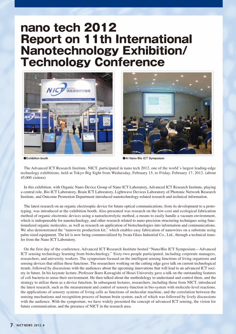
The Advanced ICT Research Institute, NICT, participated in nano tech 2012, one of the world’s largest leading-edge technology exhibitions, held at Tokyo Big Sight from Wednesday, February 15, to Friday, February 17, 2012. (about 45,000 visitors)
In this exhibition, with Organic Nano-Device Group of Nano ICT Laboratory, Advanced ICT Research Institute, playing a central role, Bio ICT Laboratory, Brain ICT Laboratory, Lightwave Devices Laboratory of Photonic Network Research Institute, and Outcome Promotion Department introduced nanotechnology-related research and technical information.
The latest research on an organic electrooptic device for future optical communications, from its development to a proto-typing, was introduced at the exhibition booth. Also presented was research on the low-cost and ecological fabrication method of organic electronic devices using a nanoelectrolytic method, a means to easily handle a vacuum environment, which is indispensable for nanotechnology, and other research related to nano-precision structuring techniques using func-tionalized organic molecules, as well as research on application of biotechnologies into information and communications. We also demonstrated the “nanowire production kit,” which enables easy fabrication of nanowires on a substrate using palm-sized equipment. The kit is now being commercialized by Iwata Glass Industrial Co., Ltd., through a technical trans-fer from the Nano ICT Laboratory.
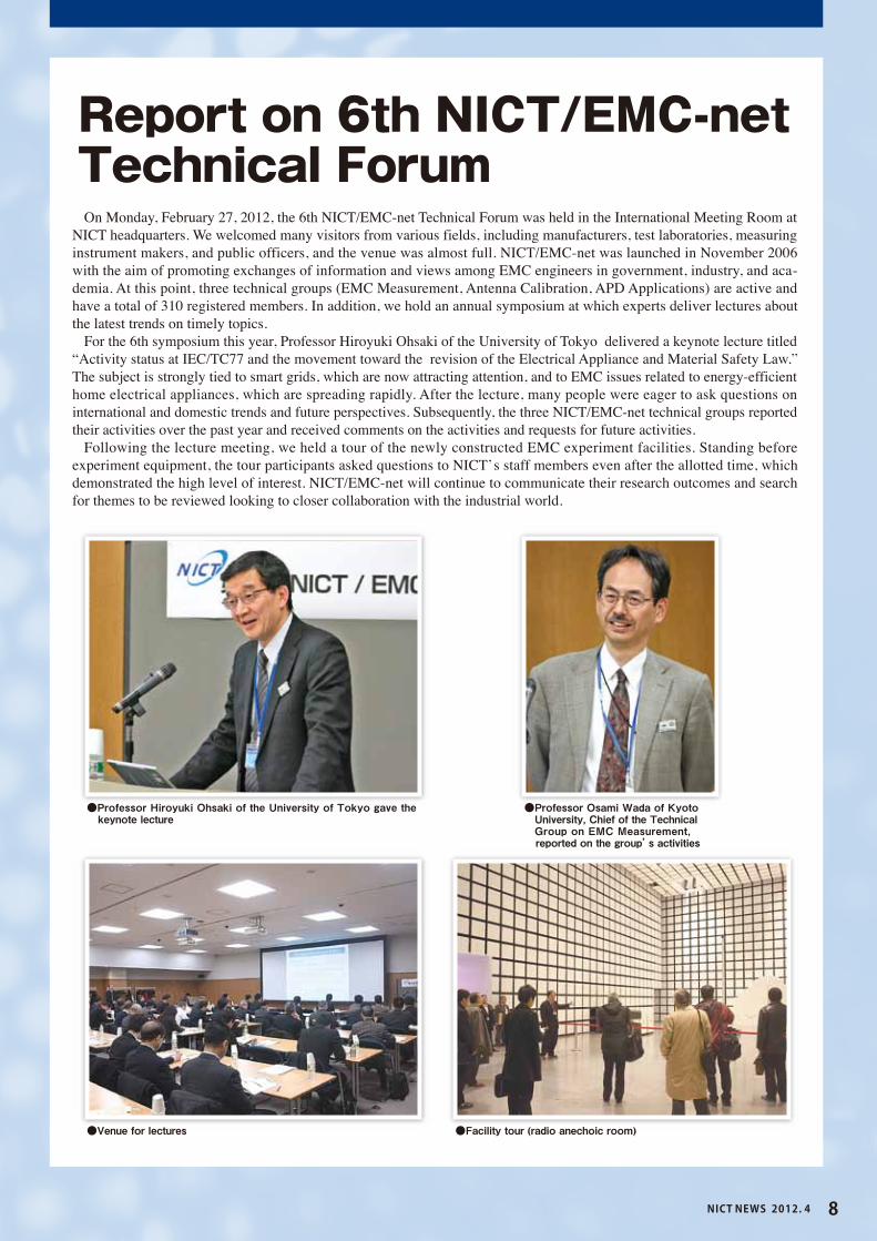
On the first day of the conference, Advanced ICT Research Institute hosted “Nano/Bio ICT Symposium—Advanced ICT sensing technology learning from biotechnology.” Sixty-two people participated, including corporate managers, researchers, and university workers. The symposium focused on the intelligent sensing functions of living organisms and sensing devices that utilize these functions. The researchers working on the cutting edge gave talk on current technological trends, followed by discussions with the audiences about the upcoming innovations that will lead to an advanced ICT soci-ety in future. In his keynote lecture, Professor Ikuro Kawagishi of Hosei University gave a talk on the outstanding features of coli bacteria to sense their environment. He then talked about the methodology to understand and control them, and the strategy to utilize them as a device function. In subsequent lectures, researchers, including those from NICT, introduced the latest research, such as the measurement and control of sensory-function in bio-system with molecule-level reactions, the applications of sensory systems of living cells as functions of molecular machine, and the correlation between the sensing mechanisms and recognition process of human brain system, each of which was followed by lively discussions with the audience. With the symposium, we have widely presented the concept of advanced ICT sensing, the vision for future communication, and the presence of NICT in the research area.
nano tech 2012Report on 11th InternationalNanotechnology Exhibition/Technology Conference
●Exhibition booth ●At Nano/Bio ICT Symposium
NICT NEWS 2012. 4 7
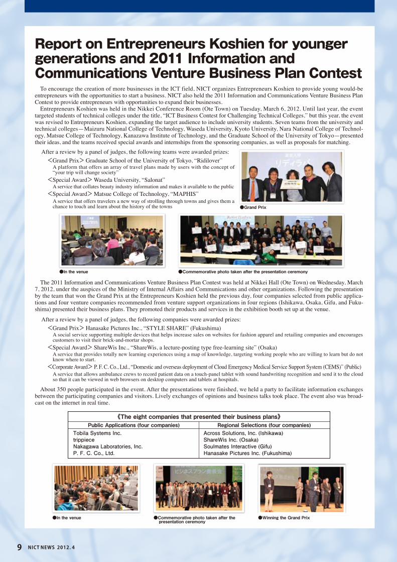
On Monday, February 27, 2012, the 6th NICT/EMC-net Technical Forum was held in the International Meeting Room at NICT headquarters. We welcomed many visitors from various fields, including manufacturers, test laboratories, measuring instrument makers, and public officers, and the venue was almost full. NICT/EMC-net was launched in November 2006 with the aim of promoting exchanges of information and views among EMC engineers in government, industry, and aca-demia. At this point, three technical groups (EMC Measurement, Antenna Calibration, APD Applications) are active and have a total of 310 registered members. In addition, we hold an annual symposium at which experts deliver lectures about the latest trends on timely topics.
For the 6th symposium this year, Professor Hiroyuki Ohsaki of the University of Tokyo delivered a keynote lecture titled “Activity status at IEC/TC77 and the movement toward the revision of the Electrical Appliance and Material Safety Law.” The subject is strongly tied to smart grids, which are now attracting attention, and to EMC issues related to energy-efficient home electrical appliances, which are spreading rapidly. After the lecture, many people were eager to ask questions on international and domestic trends and future perspectives. Subsequently, the three NICT/EMC-net technical groups reported their activities over the past year and received comments on the activities and requests for future activities.
Following the lecture meeting, we held a tour of the newly constructed EMC experiment facilities. Standing before experiment equipment, the tour participants asked questions to NICT’s staff members even after the allotted time, which demonstrated the high level of interest. NICT/EMC-net will continue to communicate their research outcomes and search for themes to be reviewed looking to closer collaboration with the industrial world.
Report on 6th NICT/EMC-netTechnical Forum
●Professor Hiroyuki Ohsaki of the University of Tokyo gave the keynote lecture
●Professor Osami Wada of Kyoto University, Chief of the Technical Group on EMC Measurement, reported on the group’s activities
●Venue for lectures ●Facility tour (radio anechoic room)
NICT NEWS 2012. 4 8
To encourage the creation of more businesses in the ICT field, NICT organizes Entrepreneurs Koshien to provide young would-be entrepreneurs with the opportunities to start a business. NICT also held the 2011 Information and Communications Venture Business Plan Contest to provide entrepreneurs with opportunities to expand their businesses.
Entrepreneurs Koshien was held in the Nikkei Conference Room (Ote Town) on Tuesday, March 6, 2012. Until last year, the event targeted students of technical colleges under the title, “ICT Business Contest for Challenging Technical Colleges,” but this year, the event was revised to Entrepreneurs Koshien, expanding the target audience to include university students. Seven teams from the university and technical colleges—Maizuru National College of Technology, Waseda University, Kyoto University, Nara National College of Technol-ogy, Matsue College of Technology, Kanazawa Institute of Technology, and the Graduate School of the University of Tokyo—presented their ideas, and the teams received special awards and internships from the sponsoring companies, as well as proposals for matching.
The 2011 Information and Communications Venture Business Plan Contest was held at Nikkei Hall (Ote Town) on Wednesday, March 7, 2012, under the auspices of the Ministry of Internal Affairs and Communications and other organizations. Following the presentation by the team that won the Grand Prix at the Entrepreneurs Koshien held the previous day, four companies selected from public applica-tions and four venture companies recommended from venture support organizations in four regions (Ishikawa, Osaka, Gifu, and Fuku-shima) presented their business plans. They promoted their products and services in the exhibition booth set up at the venue.
About 350 people participated in the event. After the presentations were finished, we held a party to facilitate information exchanges between the participating companies and visitors. Lively exchanges of opinions and business talks took place. The event also was broad-cast on the internet in real time.
Report on Entrepreneurs Koshien for youngergenerations and 2011 Information andCommunications Venture Business Plan Contest
●In the venue ●Commemorative photo taken after the presentation ceremony
●Winning the Grand Prix
●Grand Prix
●In the venue ●Commemorative photo taken after the presentation ceremony
《The eight companies that presented their business plans》Public Applications (four companies)
Tobila Systems Inc.trippieceNakagawa Laboratories, Inc.P. F. C. Co., Ltd.
Regional Selections (four companies)Across Solutions, Inc. (Ishikawa)ShareWis Inc. (Osaka)Soulmates Interactive (Gifu)Hanasake Pictures Inc. (Fukushima)
After a review by a panel of judges, the following teams were awarded prizes: <Grand Prix> Graduate School of the University of Tokyo, “Ridilover”
<Special Award> Waseda University, “Salonat”
<Special Award> Matsue College of Technology, “MAPHIS”
A platform that offers an array of travel plans made by users with the concept of “your trip will change society”
A service that offers travelers a new way of strolling through towns and gives them a chance to touch and learn about the history of the towns
A service that collates beauty industry information and makes it available to the public
After a review by a panel of judges, the following companies were awarded prizes: <Grand Prix> Hanasake Pictures Inc., “STYLE SHARE” (Fukushima)
<Special Award> ShareWis Inc., “ShareWis, a lecture-posting type free-learning site” (Osaka)
<Corporate Award> P. F. C. Co., Ltd., “Domestic and overseas deployment of Cloud Emergency Medical Service Support System (CEMS)” (Public)
A social service supporting multiple devices that helps increase sales on websites for fashion apparel and retailing companies and encourages customers to visit their brick-and-mortar shops.
A service that allows ambulance crews to record patient data on a touch-panel tablet with sound handwriting recognition and send it to the cloud so that it can be viewed in web browsers on desktop computers and tablets at hospitals.
A service that provides totally new learning experiences using a map of knowledge, targeting working people who are willing to learn but do not know where to start.
NICT NEWS 2012. 4 9
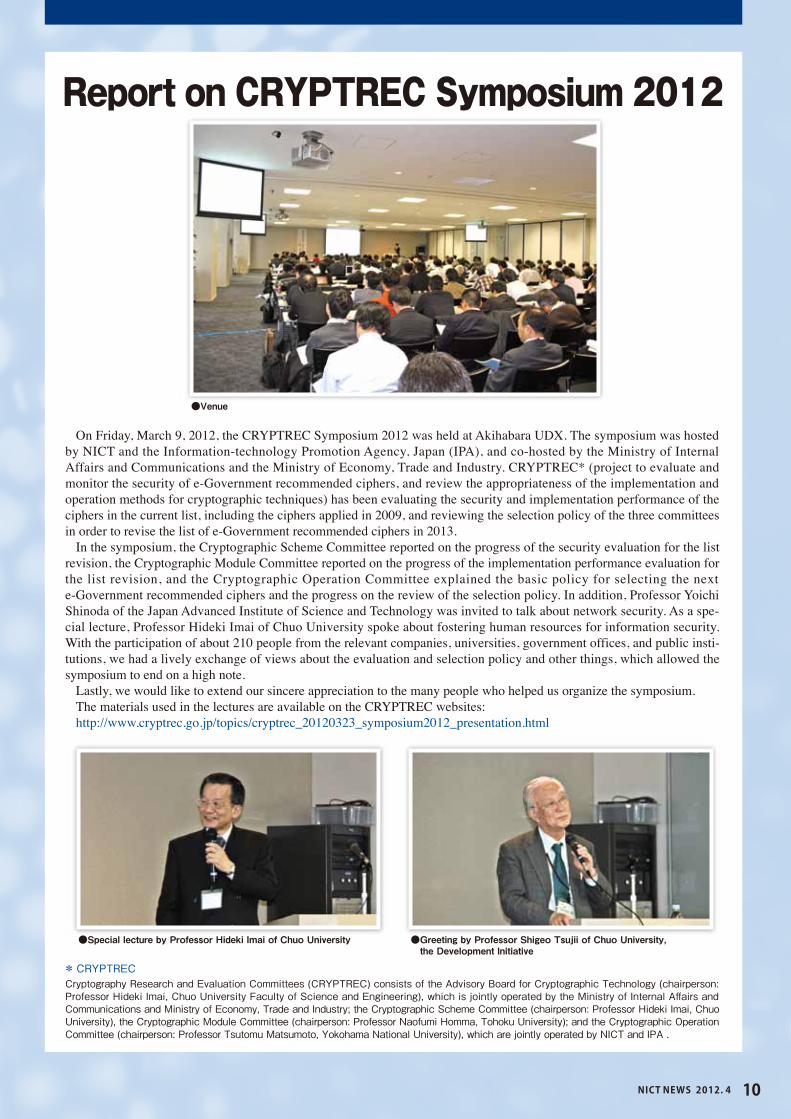
On Friday, March 9, 2012, the CRYPTREC Symposium 2012 was held at Akihabara UDX. The symposium was hosted by NICT and the Information-technology Promotion Agency, Japan (IPA), and co-hosted by the Ministry of Internal Affairs and Communications and the Ministry of Economy, Trade and Industry. CRYPTREC* (project to evaluate and monitor the security of e-Government recommended ciphers, and review the appropriateness of the implementation and operation methods for cryptographic techniques) has been evaluating the security and implementation performance of the ciphers in the current list, including the ciphers applied in 2009, and reviewing the selection policy of the three committees in order to revise the list of e-Government recommended ciphers in 2013.
In the symposium, the Cryptographic Scheme Committee reported on the progress of the security evaluation for the list revision, the Cryptographic Module Committee reported on the progress of the implementation performance evaluation for the list revision, and the Cryptographic Operation Committee explained the basic policy for selecting the next e-Government recommended ciphers and the progress on the review of the selection policy. In addition, Professor Yoichi Shinoda of the Japan Advanced Institute of Science and Technology was invited to talk about network security. As a spe-cial lecture, Professor Hideki Imai of Chuo University spoke about fostering human resources for information security. With the participation of about 210 people from the relevant companies, universities, government offices, and public insti-tutions, we had a lively exchange of views about the evaluation and selection policy and other things, which allowed the symposium to end on a high note.
Lastly, we would like to extend our sincere appreciation to the many people who helped us organize the symposium.The materials used in the lectures are available on the CRYPTREC websites:http://www.cryptrec.go.jp/topics/cryptrec_20120323_symposium2012_presentation.html
Report on CRYPTREC Symposium 2012
Cryptography Research and Evaluation Committees (CRYPTREC) consists of the Advisory Board for Cryptographic Technology (chairperson: Professor Hideki Imai, Chuo University Faculty of Science and Engineering), which is jointly operated by the Ministry of Internal Affairs and Communications and Ministry of Economy, Trade and Industry; the Cryptographic Scheme Committee (chairperson: Professor Hideki Imai, Chuo University), the Cryptographic Module Committee (chairperson: Professor Naofumi Homma, Tohoku University); and the Cryptographic Operation Committee (chairperson: Professor Tsutomu Matsumoto, Yokohama National University), which are jointly operated by NICT and IPA .
* CRYPTREC
●Venue
●Special lecture by Professor Hideki Imai of Chuo University ●Greeting by Professor Shigeo Tsujii of Chuo University, the Development Initiative
NICT NEWS 2012. 4 10
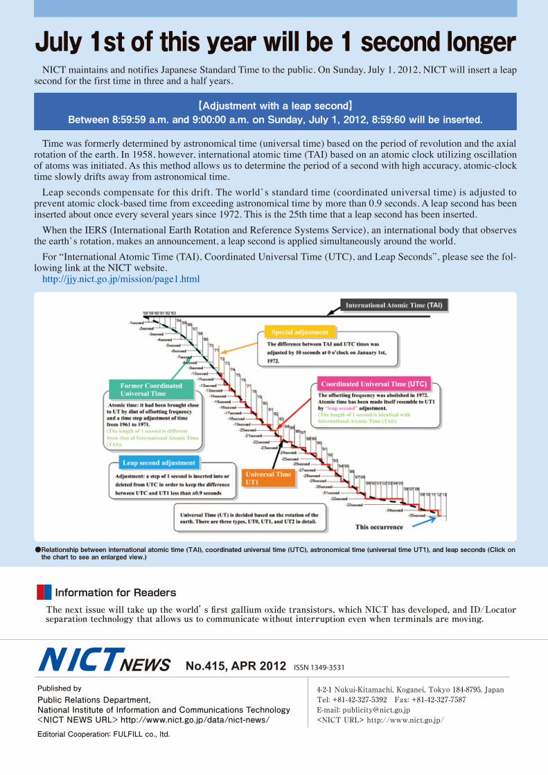
July 1st of this year will be 1 second longerNICT maintains and notifies Japanese Standard Time to the public. On Sunday, July 1, 2012, NICT will insert a leap
second for the first time in three and a half years.
Time was formerly determined by astronomical time (universal time) based on the period of revolution and the axial rotation of the earth. In 1958, however, international atomic time (TAI) based on an atomic clock utilizing oscillation of atoms was initiated. As this method allows us to determine the period of a second with high accuracy, atomic-clock time slowly drifts away from astronomical time.
Leap seconds compensate for this drift. The world’s standard time (coordinated universal time) is adjusted to prevent atomic clock-based time from exceeding astronomical time by more than 0.9 seconds. A leap second has been inserted about once every several years since 1972. This is the 25th time that a leap second has been inserted.
When the IERS (International Earth Rotation and Reference Systems Service), an international body that observes the earth’s rotation, makes an announcement, a leap second is applied simultaneously around the world.
For “International Atomic Time (TAI), Coordinated Universal Time (UTC), and Leap Seconds”, please see the fol-lowing link at the NICT website.
http://jjy.nict.go.jp/mission/page1.html
The next issue will take up the world’s first gallium oxide transistors, which NICT has developed, and ID/Locator separation technology that allows us to communicate without interruption even when terminals are moving.
Information for Readers
ISSN 1349-3531 NEWS Published byPublic Relations Department, National Institute of Information and Communications Technology <NICT NEWS URL> http://www.nict.go.jp/data/nict-news/
Editorial Cooperation: FULFILL co., ltd.
4-2-1 Nukui-Kitamachi, Koganei, Tokyo 184-8795, Japan Tel: +81-42-327-5392 Fax: +81-42-327-7587 E-mail: [email protected] <NICT URL> http://www.nict.go.jp/
No.415, APR 2012
【Adjustment with a leap second】Between 8:59:59 a.m. and 9:00:00 a.m. on Sunday, July 1, 2012, 8:59:60 will be inserted.
●Relationship between international atomic time (TAI), coordinated universal time (UTC), astronomical time (universal time UT1), and leap seconds (Click on the chart to see an enlarged view.)