Embed Size (px)
Citation preview
This is information on a product in full production.
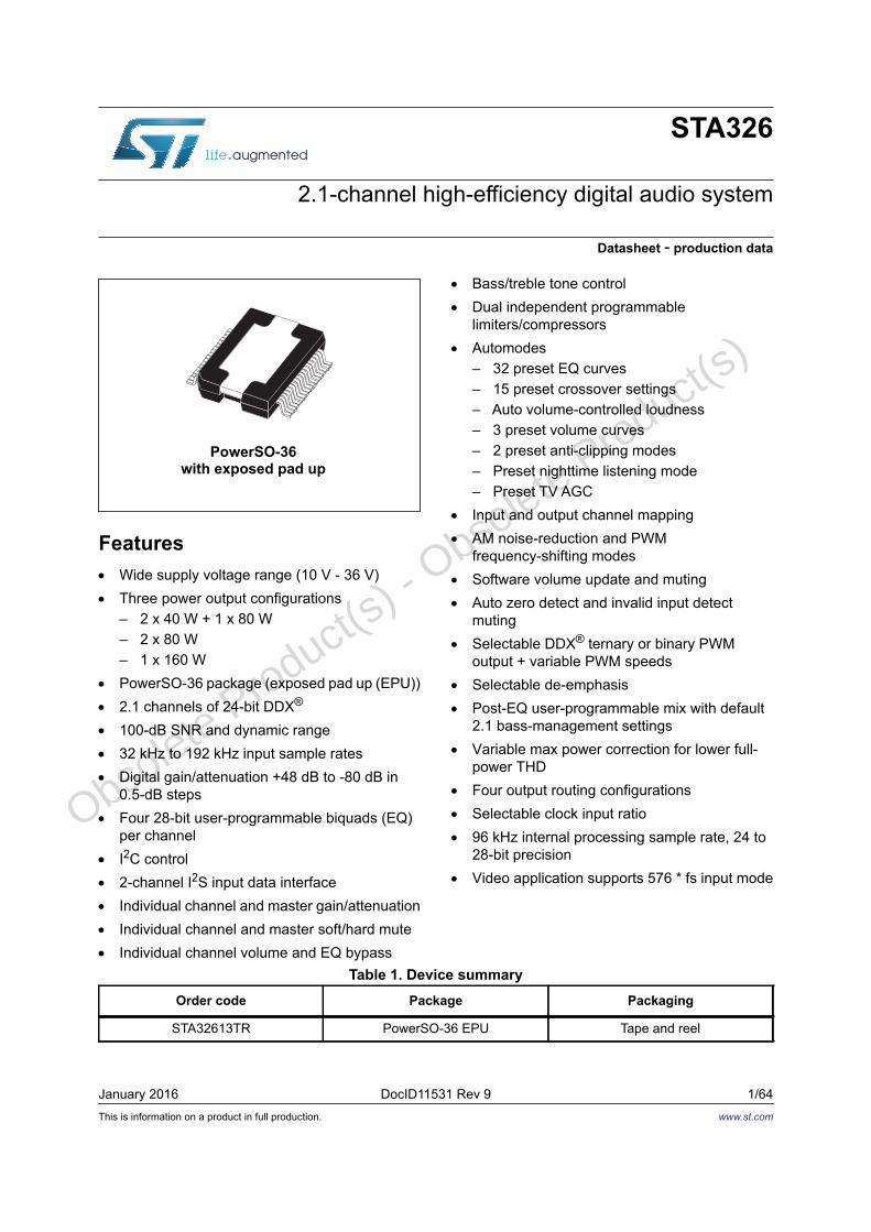
January 2016 DocID11531 Rev 9 1/64
STA326
2.1-channel high-efficiency digital audio system
Datasheet - production data
Features Wide supply voltage range (10 V - 36 V) Three power output configurations
– 2 x 40 W + 1 x 80 W– 2 x 80 W– 1 x 160 W
PowerSO-36 package (exposed pad up (EPU)) 2.1 channels of 24-bit DDX®
100-dB SNR and dynamic range 32 kHz to 192 kHz input sample rates Digital gain/attenuation +48 dB to -80 dB in
0.5-dB steps Four 28-bit user-programmable biquads (EQ)
per channel I2C control 2-channel I2S input data interface Individual channel and master gain/attenuation Individual channel and master soft/hard mute Individual channel volume and EQ bypass
Bass/treble tone control Dual independent programmable
limiters/compressors Automodes
– 32 preset EQ curves– 15 preset crossover settings– Auto volume-controlled loudness– 3 preset volume curves– 2 preset anti-clipping modes– Preset nighttime listening mode– Preset TV AGC
Input and output channel mapping AM noise-reduction and PWM
frequency-shifting modes Software volume update and muting Auto zero detect and invalid input detect
muting Selectable DDX® ternary or binary PWM
output + variable PWM speeds Selectable de-emphasis Post-EQ user-programmable mix with default
2.1 bass-management settings Variable max power correction for lower full-
power THD Four output routing configurations Selectable clock input ratio 96 kHz internal processing sample rate, 24 to
28-bit precision Video application supports 576 * fs input mode
PowerSO-36with exposed pad up
Table 1. Device summaryOrder code Package Packaging
STA32613TR PowerSO-36 EPU Tape and reel
www.st.com
O
bsolete Product(
s) - O
bsolete Product(
s)
Contents STA326
2/64 DocID11531 Rev 9
Contents
1 Description . . . . . . . . . . . . . . . . . . . . . . . . . . . . . . . . . . . . . . . . . . . . . . . . . 81.1 EQ processing . . . . . . . . . . . . . . . . . . . . . . . . . . . . . . . . . . . . . . . . . . . . . . 9
1.2 Output configurations . . . . . . . . . . . . . . . . . . . . . . . . . . . . . . . . . . . . . . . . . 9
2 Pin out . . . . . . . . . . . . . . . . . . . . . . . . . . . . . . . . . . . . . . . . . . . . . . . . . . . 102.1 Package pins . . . . . . . . . . . . . . . . . . . . . . . . . . . . . . . . . . . . . . . . . . . . . . 10
2.2 Pin list . . . . . . . . . . . . . . . . . . . . . . . . . . . . . . . . . . . . . . . . . . . . . . . . . . . . 10
2.3 Pin description . . . . . . . . . . . . . . . . . . . . . . . . . . . . . . . . . . . . . . . . . . . . . 12
3 Electrical specifications . . . . . . . . . . . . . . . . . . . . . . . . . . . . . . . . . . . . . 133.1 General interface specifications . . . . . . . . . . . . . . . . . . . . . . . . . . . . . . . . 13
3.2 DC electrical specifications (3.3 V buffers) . . . . . . . . . . . . . . . . . . . . . . . . 14
3.3 Power electrical specifications . . . . . . . . . . . . . . . . . . . . . . . . . . . . . . . . . 14
4 Power supply and control sequencing . . . . . . . . . . . . . . . . . . . . . . . . . 16
5 Characterization curves . . . . . . . . . . . . . . . . . . . . . . . . . . . . . . . . . . . . . 17
6 I2C bus specification . . . . . . . . . . . . . . . . . . . . . . . . . . . . . . . . . . . . . . . . 196.1 Communication protocol . . . . . . . . . . . . . . . . . . . . . . . . . . . . . . . . . . . . . . 19
6.2 Device addressing . . . . . . . . . . . . . . . . . . . . . . . . . . . . . . . . . . . . . . . . . . 19
6.3 Write operation . . . . . . . . . . . . . . . . . . . . . . . . . . . . . . . . . . . . . . . . . . . . . 20
6.4 Read operation . . . . . . . . . . . . . . . . . . . . . . . . . . . . . . . . . . . . . . . . . . . . . 20
7 Register description . . . . . . . . . . . . . . . . . . . . . . . . . . . . . . . . . . . . . . . . 227.1 Configuration register A (addr 0x00) . . . . . . . . . . . . . . . . . . . . . . . . . . . . 23
7.2 Configuration register B (addr 0x01) . . . . . . . . . . . . . . . . . . . . . . . . . . . . 26
7.3 Configuration register C (addr 0x02) . . . . . . . . . . . . . . . . . . . . . . . . . . . . 297.3.1 DDX® power output mode . . . . . . . . . . . . . . . . . . . . . . . . . . . . . . . . . . . 29
7.3.2 DDX® variable compensating pulse size . . . . . . . . . . . . . . . . . . . . . . . . 29
7.4 Configuration register D (addr 0x03) . . . . . . . . . . . . . . . . . . . . . . . . . . . . 30
7.5 Configuration register E (addr 0x04) . . . . . . . . . . . . . . . . . . . . . . . . . . . . 32
7.6 Configuration register F (addr 0x05) . . . . . . . . . . . . . . . . . . . . . . . . . . . . 34
O
bsolete Product(
s) - O
bsolete Product(
s)
DocID11531 Rev 9 3/64
STA326 Contents
64
7.7 Volume control . . . . . . . . . . . . . . . . . . . . . . . . . . . . . . . . . . . . . . . . . . . . . 367.7.1 Master controls . . . . . . . . . . . . . . . . . . . . . . . . . . . . . . . . . . . . . . . . . . . 36
7.7.2 Channel controls . . . . . . . . . . . . . . . . . . . . . . . . . . . . . . . . . . . . . . . . . . 36
7.7.3 Volume description . . . . . . . . . . . . . . . . . . . . . . . . . . . . . . . . . . . . . . . . 36
7.8 Automode registers . . . . . . . . . . . . . . . . . . . . . . . . . . . . . . . . . . . . . . . . . 387.8.1 Automodes EQ, volume, GC (addr 0x0B) . . . . . . . . . . . . . . . . . . . . . . . 38
7.8.2 Automode AM/prescale/bass management scale (addr 0x0C) . . . . . . . 39
7.8.3 Preset EQ settings (addr 0x0D) . . . . . . . . . . . . . . . . . . . . . . . . . . . . . . . 40
7.9 Channel configuration registers . . . . . . . . . . . . . . . . . . . . . . . . . . . . . . . . 417.9.1 Channel 1 configuration (addr 0x0E) . . . . . . . . . . . . . . . . . . . . . . . . . . . 41
7.9.2 Channel 2 configuration (addr 0x0F) . . . . . . . . . . . . . . . . . . . . . . . . . . . 41
7.9.3 Channel 3 configuration (addr 0x10) . . . . . . . . . . . . . . . . . . . . . . . . . . . 41
7.10 Tone control (addr 0x11) . . . . . . . . . . . . . . . . . . . . . . . . . . . . . . . . . . . . . . 43
7.11 Dynamics control . . . . . . . . . . . . . . . . . . . . . . . . . . . . . . . . . . . . . . . . . . . 447.11.1 Limiter 1 attack/release threshold (addr 0x12) . . . . . . . . . . . . . . . . . . . 44
7.11.2 Limiter 1 attack/release threshold (addr 0x13) . . . . . . . . . . . . . . . . . . . 44
7.11.3 Limiter 2 attack/release rate (addr 0x14) . . . . . . . . . . . . . . . . . . . . . . . . 44
7.11.4 Limiter 2 attack/release threshold (addr 0x15) . . . . . . . . . . . . . . . . . . . 44
7.11.5 Dynamics control description . . . . . . . . . . . . . . . . . . . . . . . . . . . . . . . . . 44
7.11.6 Anti-clipping mode . . . . . . . . . . . . . . . . . . . . . . . . . . . . . . . . . . . . . . . . . 46
7.11.7 Dynamic range compression mode . . . . . . . . . . . . . . . . . . . . . . . . . . . . 47
8 User programmable processing . . . . . . . . . . . . . . . . . . . . . . . . . . . . . . 488.1 EQ - biquad equation . . . . . . . . . . . . . . . . . . . . . . . . . . . . . . . . . . . . . . . . 48
8.2 Prescale . . . . . . . . . . . . . . . . . . . . . . . . . . . . . . . . . . . . . . . . . . . . . . . . . . 48
8.3 Postscale . . . . . . . . . . . . . . . . . . . . . . . . . . . . . . . . . . . . . . . . . . . . . . . . . 48
8.4 Mix/bass management . . . . . . . . . . . . . . . . . . . . . . . . . . . . . . . . . . . . . . . 49
8.5 Calculating 24-bit signed fractional numbers from a dB value . . . . . . . . . 50
8.6 User-defined coefficient RAM . . . . . . . . . . . . . . . . . . . . . . . . . . . . . . . . . . 508.6.1 Coefficient address register 1 (addr 0x16) . . . . . . . . . . . . . . . . . . . . . . . 50
8.6.2 Coefficient b1data register bits 23:16 (addr 0x17) . . . . . . . . . . . . . . . . . 50
8.6.3 Coefficient b1data register bits 15:8 (addr 0x18) . . . . . . . . . . . . . . . . . . 50
8.6.4 Coefficient b1data register bits 7:0 (addr 0x19) . . . . . . . . . . . . . . . . . . . 50
8.6.5 Coefficient b2 data register bits 23:16 (addr 0x1A) . . . . . . . . . . . . . . . . 50
8.6.6 Coefficient b2 data register bits 15:8 (addr 0x1B) . . . . . . . . . . . . . . . . . 51
8.6.7 Coefficient b2 data register bits 7:0 (addr 0x1C) . . . . . . . . . . . . . . . . . . 51
O
bsolete Product(
s) - O
bsolete Product(
s)
Contents STA326
4/64 DocID11531 Rev 9
8.6.8 Coefficient a1 data register bits 23:16 (addr 0x1D) . . . . . . . . . . . . . . . . 51
8.6.9 Coefficient a1 data register bits 15:8 (addr 0x1E) . . . . . . . . . . . . . . . . . 51
8.6.10 Coefficient a1 data register bits 7:0 (addr 0x1F) . . . . . . . . . . . . . . . . . . 51
8.6.11 Coefficient a2 data register bits 23:16 (addr 0x20) . . . . . . . . . . . . . . . . 51
8.6.12 Coefficient a2 data register bits 15:8 (addr 0x21) . . . . . . . . . . . . . . . . . 51
8.6.13 Coefficient a2 data register bits 7:0 (addr 0x22) . . . . . . . . . . . . . . . . . . 51
8.6.14 Coefficient b0 data register bits 23:16 (addr 0x23) . . . . . . . . . . . . . . . . 52
8.6.15 Coefficient b0 data register bits 15:8 (addr 0x24) . . . . . . . . . . . . . . . . . 52
8.6.16 Coefficient b0 data register bits 7:0 (addr 0x25) . . . . . . . . . . . . . . . . . . 52
8.6.17 Coefficient write control register (addr 0x26) . . . . . . . . . . . . . . . . . . . . . 52
8.7 Reading a coefficient from RAM . . . . . . . . . . . . . . . . . . . . . . . . . . . . . . . . 53
8.8 Reading a set of coefficients from RAM . . . . . . . . . . . . . . . . . . . . . . . . . . 53
8.9 Writing a single coefficient to RAM . . . . . . . . . . . . . . . . . . . . . . . . . . . . . . 53
8.10 Writing a set of coefficients to RAM . . . . . . . . . . . . . . . . . . . . . . . . . . . . . 54
8.11 Variable max power correction (addr 0x27, 0x28) . . . . . . . . . . . . . . . . . . 56
8.12 Fault detect recovery (addr 0x2B, 0x2C) . . . . . . . . . . . . . . . . . . . . . . . . . 56
8.13 Status (addr 0x2D) . . . . . . . . . . . . . . . . . . . . . . . . . . . . . . . . . . . . . . . . . . 56
9 Applications . . . . . . . . . . . . . . . . . . . . . . . . . . . . . . . . . . . . . . . . . . . . . . . 57
10 Package mechanical data . . . . . . . . . . . . . . . . . . . . . . . . . . . . . . . . . . . . 6010.1 PowerSO-36 EPU package information . . . . . . . . . . . . . . . . . . . . . . . . . . 61
11 Revision history . . . . . . . . . . . . . . . . . . . . . . . . . . . . . . . . . . . . . . . . . . . 63
O
bsolete Product(
s) - O
bsolete Product(
s)
DocID11531 Rev 9 5/64
STA326 List of tables
64
List of tables
Table 1. Device summary . . . . . . . . . . . . . . . . . . . . . . . . . . . . . . . . . . . . . . . . . . . . . . . . . . . . . . . . . . 1Table 2. Pin list . . . . . . . . . . . . . . . . . . . . . . . . . . . . . . . . . . . . . . . . . . . . . . . . . . . . . . . . . . . . . . . . . 10Table 3. Absolute maximum ratings . . . . . . . . . . . . . . . . . . . . . . . . . . . . . . . . . . . . . . . . . . . . . . . . . 13Table 4. Thermal data. . . . . . . . . . . . . . . . . . . . . . . . . . . . . . . . . . . . . . . . . . . . . . . . . . . . . . . . . . . . 13Table 5. Recommended operating conditions . . . . . . . . . . . . . . . . . . . . . . . . . . . . . . . . . . . . . . . . . 13Table 6. General interface electrical characteristics . . . . . . . . . . . . . . . . . . . . . . . . . . . . . . . . . . . . . 13Table 7. DC electrical specifications. . . . . . . . . . . . . . . . . . . . . . . . . . . . . . . . . . . . . . . . . . . . . . . . . 14Table 8. Power electrical characteristics. . . . . . . . . . . . . . . . . . . . . . . . . . . . . . . . . . . . . . . . . . . . . . 14Table 9. Register summary. . . . . . . . . . . . . . . . . . . . . . . . . . . . . . . . . . . . . . . . . . . . . . . . . . . . . . . . 22Table 10. Master clock select . . . . . . . . . . . . . . . . . . . . . . . . . . . . . . . . . . . . . . . . . . . . . . . . . . . . . . . 23Table 11. IR and MCS settings for input sample rate and clock rate . . . . . . . . . . . . . . . . . . . . . . . . . 24Table 12. Interpolation ratio select . . . . . . . . . . . . . . . . . . . . . . . . . . . . . . . . . . . . . . . . . . . . . . . . . . . 24Table 13. IR bit settings as a function of input sample rate . . . . . . . . . . . . . . . . . . . . . . . . . . . . . . . . 24Table 14. Thermal warning recovery bypass . . . . . . . . . . . . . . . . . . . . . . . . . . . . . . . . . . . . . . . . . . . 24Table 15. Thermal warning adjustment bypass . . . . . . . . . . . . . . . . . . . . . . . . . . . . . . . . . . . . . . . . . 25Table 16. Fault detect recovery bypass . . . . . . . . . . . . . . . . . . . . . . . . . . . . . . . . . . . . . . . . . . . . . . . 25Table 17. Serial audio input interface format . . . . . . . . . . . . . . . . . . . . . . . . . . . . . . . . . . . . . . . . . . . 26Table 18. Supported serial audio input formats . . . . . . . . . . . . . . . . . . . . . . . . . . . . . . . . . . . . . . . . . 27Table 19. Serial input data timing characteristics (fs = 32 to 192 kHz). . . . . . . . . . . . . . . . . . . . . . . . 28Table 20. Delay serial clock enable . . . . . . . . . . . . . . . . . . . . . . . . . . . . . . . . . . . . . . . . . . . . . . . . . . 28Table 21. Channel input mapping. . . . . . . . . . . . . . . . . . . . . . . . . . . . . . . . . . . . . . . . . . . . . . . . . . . . 28Table 22. DDX® power output mode . . . . . . . . . . . . . . . . . . . . . . . . . . . . . . . . . . . . . . . . . . . . . . . . . 29Table 23. DDX® output modes . . . . . . . . . . . . . . . . . . . . . . . . . . . . . . . . . . . . . . . . . . . . . . . . . . . . . . 29Table 24. DDX® compensating pulse . . . . . . . . . . . . . . . . . . . . . . . . . . . . . . . . . . . . . . . . . . . . . . . . . 29Table 25. High-pass filter bypass . . . . . . . . . . . . . . . . . . . . . . . . . . . . . . . . . . . . . . . . . . . . . . . . . . . . 30Table 26. De-emphasis. . . . . . . . . . . . . . . . . . . . . . . . . . . . . . . . . . . . . . . . . . . . . . . . . . . . . . . . . . . . 30Table 27. DSP bypass . . . . . . . . . . . . . . . . . . . . . . . . . . . . . . . . . . . . . . . . . . . . . . . . . . . . . . . . . . . . 30Table 28. Postscale link . . . . . . . . . . . . . . . . . . . . . . . . . . . . . . . . . . . . . . . . . . . . . . . . . . . . . . . . . . . 30Table 29. Biquad coefficient link . . . . . . . . . . . . . . . . . . . . . . . . . . . . . . . . . . . . . . . . . . . . . . . . . . . . . 31Table 30. Dynamic range compression/anti-clipping bit . . . . . . . . . . . . . . . . . . . . . . . . . . . . . . . . . . . 31Table 31. Zero detect mute enable. . . . . . . . . . . . . . . . . . . . . . . . . . . . . . . . . . . . . . . . . . . . . . . . . . . 31Table 32. Miami mode enable. . . . . . . . . . . . . . . . . . . . . . . . . . . . . . . . . . . . . . . . . . . . . . . . . . . . . . . 31Table 33. Max power correction variable . . . . . . . . . . . . . . . . . . . . . . . . . . . . . . . . . . . . . . . . . . . . . . 32Table 34. Max power correction . . . . . . . . . . . . . . . . . . . . . . . . . . . . . . . . . . . . . . . . . . . . . . . . . . . . . 32Table 35. AM mode enable. . . . . . . . . . . . . . . . . . . . . . . . . . . . . . . . . . . . . . . . . . . . . . . . . . . . . . . . . 32Table 36. PWM speed mode . . . . . . . . . . . . . . . . . . . . . . . . . . . . . . . . . . . . . . . . . . . . . . . . . . . . . . . 32Table 37. Zero-crossing volume enable . . . . . . . . . . . . . . . . . . . . . . . . . . . . . . . . . . . . . . . . . . . . . . . 33Table 38. Soft volume update enable . . . . . . . . . . . . . . . . . . . . . . . . . . . . . . . . . . . . . . . . . . . . . . . . . 33Table 39. Output configuration selection . . . . . . . . . . . . . . . . . . . . . . . . . . . . . . . . . . . . . . . . . . . . . . 34Table 40. Output configuration selection . . . . . . . . . . . . . . . . . . . . . . . . . . . . . . . . . . . . . . . . . . . . . . 34Table 41. Invalid input detect mute enable . . . . . . . . . . . . . . . . . . . . . . . . . . . . . . . . . . . . . . . . . . . . . 34Table 42. Binary clock loss detection enable . . . . . . . . . . . . . . . . . . . . . . . . . . . . . . . . . . . . . . . . . . . 34Table 43. Auto-EAPD on clock loss enable . . . . . . . . . . . . . . . . . . . . . . . . . . . . . . . . . . . . . . . . . . . . 35Table 44. Software power down . . . . . . . . . . . . . . . . . . . . . . . . . . . . . . . . . . . . . . . . . . . . . . . . . . . . . 35Table 45. External amplifier power down . . . . . . . . . . . . . . . . . . . . . . . . . . . . . . . . . . . . . . . . . . . . . . 35Table 46. Master volume offset as a function of MV[7:0] . . . . . . . . . . . . . . . . . . . . . . . . . . . . . . . . . . 37Table 47. Channel volume as a function of CxV[7:0] . . . . . . . . . . . . . . . . . . . . . . . . . . . . . . . . . . . . . 37Table 48. Automode EQ . . . . . . . . . . . . . . . . . . . . . . . . . . . . . . . . . . . . . . . . . . . . . . . . . . . . . . . . . . . 38
O
bsolete Product(
s) - O
bsolete Product(
s)
List of tables STA326
6/64 DocID11531 Rev 9
Table 49. Automode volume. . . . . . . . . . . . . . . . . . . . . . . . . . . . . . . . . . . . . . . . . . . . . . . . . . . . . . . . 38Table 50. Automode gain compression/limiters . . . . . . . . . . . . . . . . . . . . . . . . . . . . . . . . . . . . . . . . . 38Table 51. AMPS - Automode auto prescale . . . . . . . . . . . . . . . . . . . . . . . . . . . . . . . . . . . . . . . . . . . . 38Table 52. Automode AM switching enable . . . . . . . . . . . . . . . . . . . . . . . . . . . . . . . . . . . . . . . . . . . . . 39Table 53. Automode AM switching frequency selection . . . . . . . . . . . . . . . . . . . . . . . . . . . . . . . . . . . 39Table 54. Automode crossover setting . . . . . . . . . . . . . . . . . . . . . . . . . . . . . . . . . . . . . . . . . . . . . . . . 39Table 55. Crossover frequency selection . . . . . . . . . . . . . . . . . . . . . . . . . . . . . . . . . . . . . . . . . . . . . . 39Table 56. Preset EQ selection . . . . . . . . . . . . . . . . . . . . . . . . . . . . . . . . . . . . . . . . . . . . . . . . . . . . . . 40Table 57. Channel limiter mapping selection . . . . . . . . . . . . . . . . . . . . . . . . . . . . . . . . . . . . . . . . . . . 42Table 58. Channel PWM output mapping. . . . . . . . . . . . . . . . . . . . . . . . . . . . . . . . . . . . . . . . . . . . . . 42Table 59. Tone control boost/cut selection . . . . . . . . . . . . . . . . . . . . . . . . . . . . . . . . . . . . . . . . . . . . . 43Table 60. Limiter attack/release rate selection . . . . . . . . . . . . . . . . . . . . . . . . . . . . . . . . . . . . . . . . . . 45Table 61. Limiter attack/release threshold selection (AC mode) . . . . . . . . . . . . . . . . . . . . . . . . . . . . 46Table 62. Limiter attack/release threshold selection (DRC mode) . . . . . . . . . . . . . . . . . . . . . . . . . . . 47Table 63. RAM block for biquads, mixing, and scaling . . . . . . . . . . . . . . . . . . . . . . . . . . . . . . . . . . . . 54Table 64. TWARN. . . . . . . . . . . . . . . . . . . . . . . . . . . . . . . . . . . . . . . . . . . . . . . . . . . . . . . . . . . . . . . . 56Table 65. FAULT . . . . . . . . . . . . . . . . . . . . . . . . . . . . . . . . . . . . . . . . . . . . . . . . . . . . . . . . . . . . . . . . 56Table 66. PLLUL. . . . . . . . . . . . . . . . . . . . . . . . . . . . . . . . . . . . . . . . . . . . . . . . . . . . . . . . . . . . . . . . . 56Table 67. PowerSO-36 EPU package mechanical data . . . . . . . . . . . . . . . . . . . . . . . . . . . . . . . . . . . 62Table 68. Document revision history. . . . . . . . . . . . . . . . . . . . . . . . . . . . . . . . . . . . . . . . . . . . . . . . . . 63
O
bsolete Product(
s) - O
bsolete Product(
s)
DocID11531 Rev 9 7/64
STA326 List of figures
64
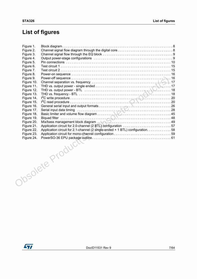
List of figures
Figure 1. Block diagram . . . . . . . . . . . . . . . . . . . . . . . . . . . . . . . . . . . . . . . . . . . . . . . . . . . . . . . . . . . . 8Figure 2. Channel signal flow diagram through the digital core . . . . . . . . . . . . . . . . . . . . . . . . . . . . . . 8Figure 3. Channel signal flow through the EQ block . . . . . . . . . . . . . . . . . . . . . . . . . . . . . . . . . . . . . . 9Figure 4. Output power-stage configurations . . . . . . . . . . . . . . . . . . . . . . . . . . . . . . . . . . . . . . . . . . . 9Figure 5. Pin connections . . . . . . . . . . . . . . . . . . . . . . . . . . . . . . . . . . . . . . . . . . . . . . . . . . . . . . . . . 10Figure 6. Test circuit 1 . . . . . . . . . . . . . . . . . . . . . . . . . . . . . . . . . . . . . . . . . . . . . . . . . . . . . . . . . . . . 15Figure 7. Test circuit 2 . . . . . . . . . . . . . . . . . . . . . . . . . . . . . . . . . . . . . . . . . . . . . . . . . . . . . . . . . . . . 15Figure 8. Power-on sequence . . . . . . . . . . . . . . . . . . . . . . . . . . . . . . . . . . . . . . . . . . . . . . . . . . . . . . 16Figure 9. Power-off sequence . . . . . . . . . . . . . . . . . . . . . . . . . . . . . . . . . . . . . . . . . . . . . . . . . . . . . . 16Figure 10. Channel separation vs. frequency . . . . . . . . . . . . . . . . . . . . . . . . . . . . . . . . . . . . . . . . . . . 17Figure 11. THD vs. output power - single ended . . . . . . . . . . . . . . . . . . . . . . . . . . . . . . . . . . . . . . . . . 17Figure 12. THD vs. output power - BTL . . . . . . . . . . . . . . . . . . . . . . . . . . . . . . . . . . . . . . . . . . . . . . . 18Figure 13. THD vs. frequency - BTL . . . . . . . . . . . . . . . . . . . . . . . . . . . . . . . . . . . . . . . . . . . . . . . . . . 18Figure 14. I2C write procedure. . . . . . . . . . . . . . . . . . . . . . . . . . . . . . . . . . . . . . . . . . . . . . . . . . . . . . . 20Figure 15. I2C read procedure . . . . . . . . . . . . . . . . . . . . . . . . . . . . . . . . . . . . . . . . . . . . . . . . . . . . . . . 20Figure 16. General serial input and output formats . . . . . . . . . . . . . . . . . . . . . . . . . . . . . . . . . . . . . . . 26Figure 17. Serial input data timing . . . . . . . . . . . . . . . . . . . . . . . . . . . . . . . . . . . . . . . . . . . . . . . . . . . 28Figure 18. Basic limiter and volume flow diagram . . . . . . . . . . . . . . . . . . . . . . . . . . . . . . . . . . . . . . . . 45Figure 19. Biquad filter . . . . . . . . . . . . . . . . . . . . . . . . . . . . . . . . . . . . . . . . . . . . . . . . . . . . . . . . . . . . 48Figure 20. Mix/bass management block diagram . . . . . . . . . . . . . . . . . . . . . . . . . . . . . . . . . . . . . . . . 49Figure 21. Application circuit for 2.0-channel (2 BTL) configuration . . . . . . . . . . . . . . . . . . . . . . . . . . 57Figure 22. Application circuit for 2.1-channel (2 single-ended + 1 BTL) configuration. . . . . . . . . . . . . 58Figure 23. Application circuit for mono-channel configuration . . . . . . . . . . . . . . . . . . . . . . . . . . . . . . . 59Figure 24. PowerSO-36 EPU package outline. . . . . . . . . . . . . . . . . . . . . . . . . . . . . . . . . . . . . . . . . . . 61
O
bsolete Product(
s) - O
bsolete Product(
s)
Description STA326
8/64 DocID11531 Rev 9
1 Description
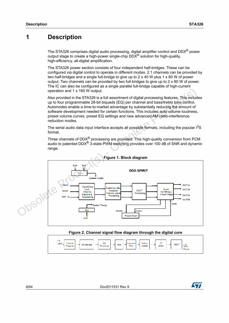
The STA326 comprises digital audio processing, digital amplifier control and DDX® power output stage to create a high-power single-chip DDX® solution for high-quality, high-efficiency, all-digital amplification.
The STA326 power section consists of four independent half-bridges. These can be configured via digital control to operate in different modes. 2.1 channels can be provided by two half-bridges and a single full-bridge to give up to 2 x 40 W plus 1 x 80 W of power output. Two channels can be provided by two full-bridges to give up to 2 x 80 W of power. The IC can also be configured as a single parallel full-bridge capable of high-current operation and 1 x 160 W output.
Also provided in the STA326 is a full assortment of digital processing features. This includes up to four programmable 28-bit biquads (EQ) per channel and bass/treble tone control. Automodes enable a time-to-market advantage by substantially reducing the amount of software development needed for certain functions. This includes auto volume loudness, preset volume curves, preset EQ settings and new advanced AM radio-interference reduction modes.
The serial audio data input interface accepts all possible formats, including the popular I2S format.
Three channels of DDX® processing are provided. This high-quality conversion from PCM audio to patented DDX® 3-state PWM switching provides over 100 dB of SNR and dynamic range.
Figure 1. Block diagram
Figure 2. Channel signal flow diagram through the digital core
Obso
lete Product(s)
- Obso
lete Product(s)
DocID11531 Rev 9 9/64
STA326 Description
64
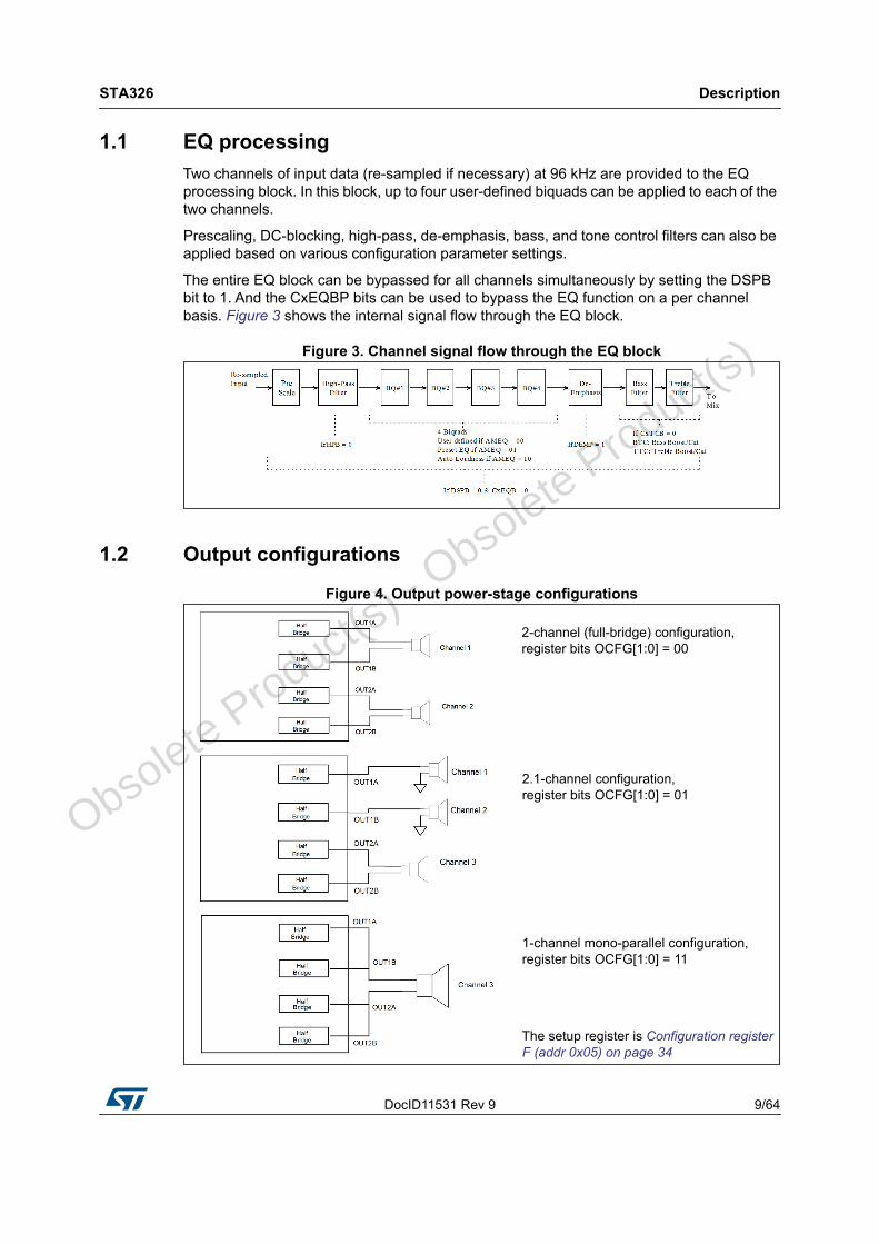
1.1 EQ processingTwo channels of input data (re-sampled if necessary) at 96 kHz are provided to the EQ processing block. In this block, up to four user-defined biquads can be applied to each of the two channels.
Prescaling, DC-blocking, high-pass, de-emphasis, bass, and tone control filters can also be applied based on various configuration parameter settings.
The entire EQ block can be bypassed for all channels simultaneously by setting the DSPB bit to 1. And the CxEQBP bits can be used to bypass the EQ function on a per channel basis. Figure 3 shows the internal signal flow through the EQ block.
Figure 3. Channel signal flow through the EQ block
1.2 Output configurations
Figure 4. Output power-stage configurations
2-channel (full-bridge) configuration, register bits OCFG[1:0] = 00
2.1-channel configuration,register bits OCFG[1:0] = 01
1-channel mono-parallel configuration, register bits OCFG[1:0] = 11
The setup register is Configuration register F (addr 0x05) on page 34
O
bsolete Product(
s) - O
bsolete Product(
s)
Pin out STA326
10/64 DocID11531 Rev 9
2 Pin out
2.1 Package pins
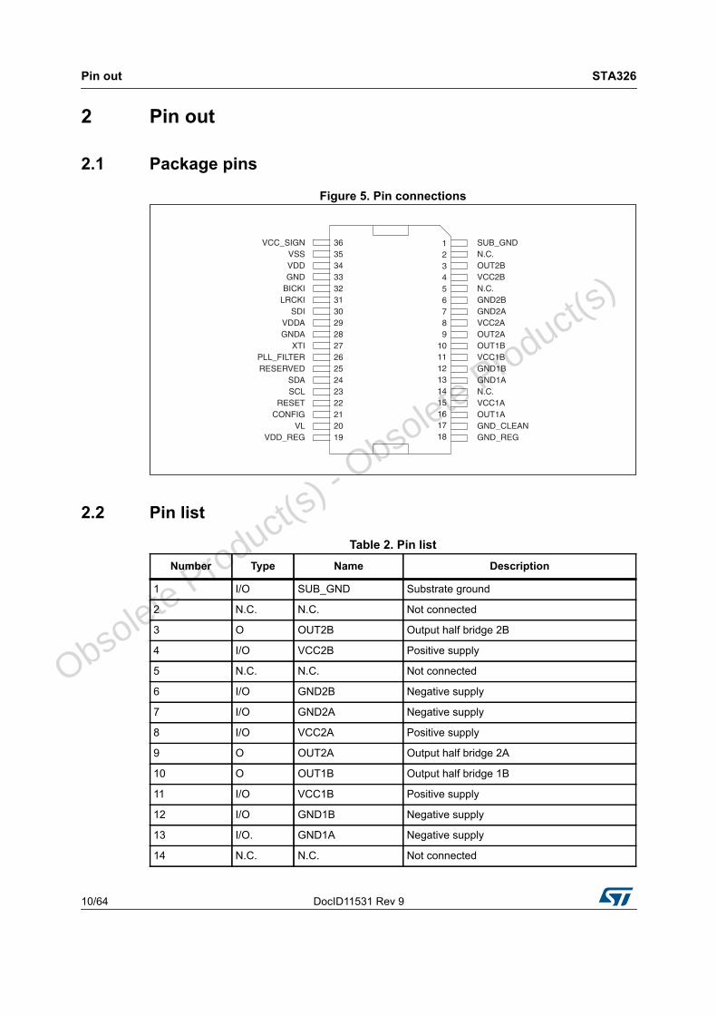
Figure 5. Pin connections
2.2 Pin list
VCC_SIGNVSSVDDGND
BICKILRCKI
SDIVDDAGNDA
XTIPLL_FILTERRESERVED
SDASCL
RESETCONFIG
VLVDD_REG
SUB_GNDN.C.OUT2BVCC2BN.C.GND2BGND2AVCC2AOUT2AOUT1BVCC1BGND1BGND1AN.C.VCC1AOUT1AGND_CLEANGND_REG
363534333231302928272625242322212019
123456789
101112131415161718
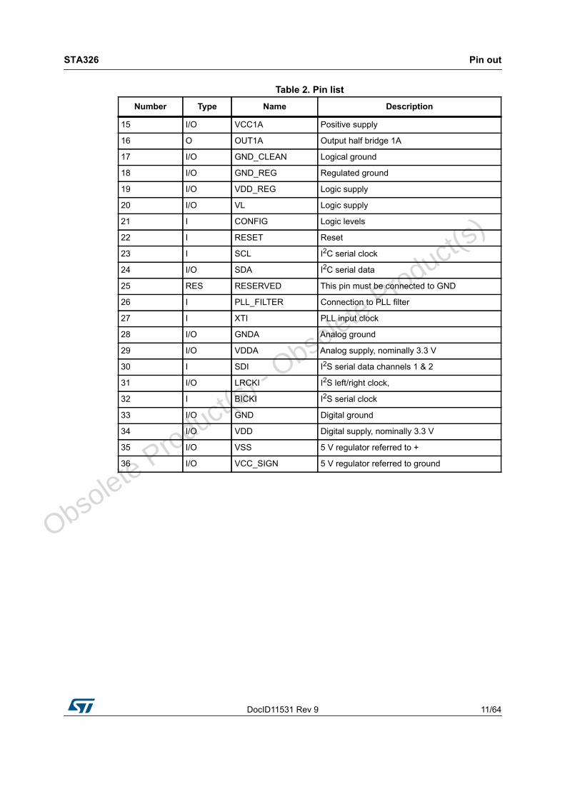
Table 2. Pin list Number Type Name Description
1 I/O SUB_GND Substrate ground
2 N.C. N.C. Not connected
3 O OUT2B Output half bridge 2B
4 I/O VCC2B Positive supply
5 N.C. N.C. Not connected
6 I/O GND2B Negative supply
7 I/O GND2A Negative supply
8 I/O VCC2A Positive supply
9 O OUT2A Output half bridge 2A
10 O OUT1B Output half bridge 1B
11 I/O VCC1B Positive supply
12 I/O GND1B Negative supply
13 I/O. GND1A Negative supply
14 N.C. N.C. Not connected
O
bsolete Product(
s) - O
bsolete Product(
s)
DocID11531 Rev 9 11/64
STA326 Pin out
64
15 I/O VCC1A Positive supply
16 O OUT1A Output half bridge 1A
17 I/O GND_CLEAN Logical ground
18 I/O GND_REG Regulated ground
19 I/O VDD_REG Logic supply
20 I/O VL Logic supply
21 I CONFIG Logic levels
22 I RESET Reset
23 I SCL I2C serial clock
24 I/O SDA I2C serial data
25 RES RESERVED This pin must be connected to GND
26 I PLL_FILTER Connection to PLL filter
27 I XTI PLL input clock
28 I/O GNDA Analog ground
29 I/O VDDA Analog supply, nominally 3.3 V
30 I SDI I2S serial data channels 1 & 2
31 I/O LRCKI I2S left/right clock,
32 I BICKI I2S serial clock
33 I/O GND Digital ground
34 I/O VDD Digital supply, nominally 3.3 V
35 I/O VSS 5 V regulator referred to +
36 I/O VCC_SIGN 5 V regulator referred to ground
Table 2. Pin list Number Type Name Description
O
bsolete Product(
s) - O
bsolete Product(
s)
Pin out STA326
12/64 DocID11531 Rev 9
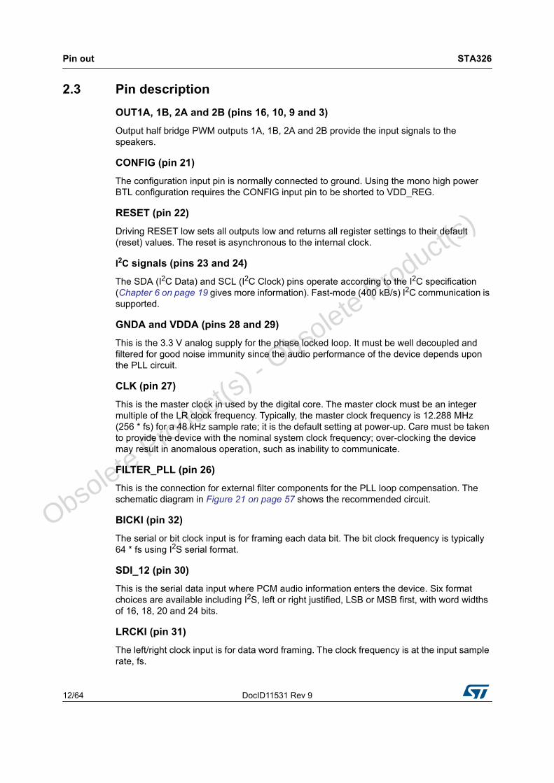
2.3 Pin descriptionOUT1A, 1B, 2A and 2B (pins 16, 10, 9 and 3)
Output half bridge PWM outputs 1A, 1B, 2A and 2B provide the input signals to the speakers.
CONFIG (pin 21)
The configuration input pin is normally connected to ground. Using the mono high power BTL configuration requires the CONFIG input pin to be shorted to VDD_REG.
RESET (pin 22)
Driving RESET low sets all outputs low and returns all register settings to their default (reset) values. The reset is asynchronous to the internal clock.
I2C signals (pins 23 and 24)
The SDA (I2C Data) and SCL (I2C Clock) pins operate according to the I2C specification (Chapter 6 on page 19 gives more information). Fast-mode (400 kB/s) I2C communication is supported.
GNDA and VDDA (pins 28 and 29)
This is the 3.3 V analog supply for the phase locked loop. It must be well decoupled and filtered for good noise immunity since the audio performance of the device depends upon the PLL circuit.
CLK (pin 27)
This is the master clock in used by the digital core. The master clock must be an integer multiple of the LR clock frequency. Typically, the master clock frequency is 12.288 MHz (256 * fs) for a 48 kHz sample rate; it is the default setting at power-up. Care must be taken to provide the device with the nominal system clock frequency; over-clocking the device may result in anomalous operation, such as inability to communicate.
FILTER_PLL (pin 26)
This is the connection for external filter components for the PLL loop compensation. The schematic diagram in Figure 21 on page 57 shows the recommended circuit.
BICKI (pin 32)
The serial or bit clock input is for framing each data bit. The bit clock frequency is typically 64 * fs using I2S serial format.
SDI_12 (pin 30)
This is the serial data input where PCM audio information enters the device. Six format choices are available including I2S, left or right justified, LSB or MSB first, with word widths of 16, 18, 20 and 24 bits.
LRCKI (pin 31)
The left/right clock input is for data word framing. The clock frequency is at the input sample rate, fs.
O
bsolete Product(
s) - O
bsolete Product(
s)
DocID11531 Rev 9 13/64
STA326 Electrical specifications
64
3 Electrical specifications
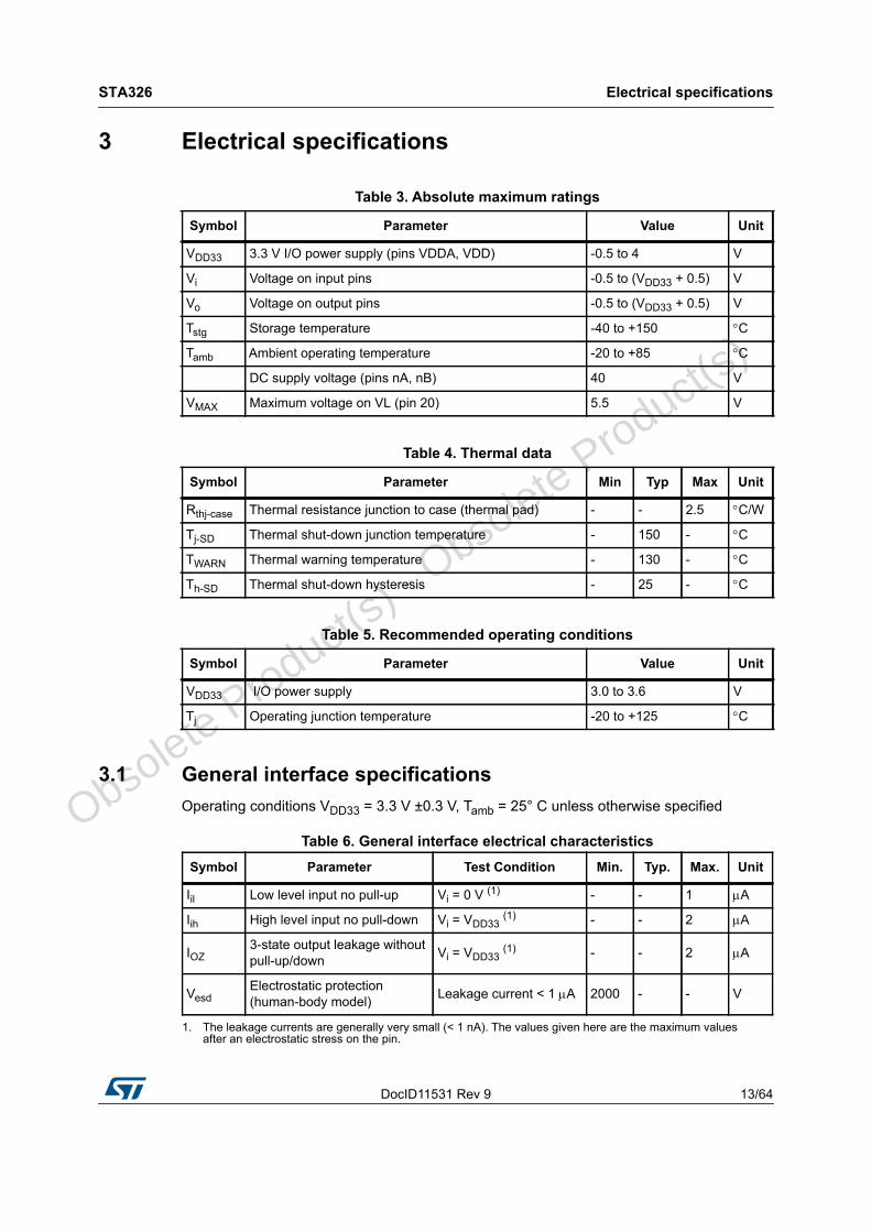
Table 3. Absolute maximum ratings
Table 4. Thermal data
Table 5. Recommended operating conditions
3.1 General interface specificationsOperating conditions VDD33 = 3.3 V ±0.3 V, Tamb = 25° C unless otherwise specified
Symbol Parameter Value Unit
VDD33 3.3 V I/O power supply (pins VDDA, VDD) -0.5 to 4 V
Vi Voltage on input pins -0.5 to (VDD33 + 0.5) V
Vo Voltage on output pins -0.5 to (VDD33 + 0.5) V
Tstg Storage temperature -40 to +150 C
Tamb Ambient operating temperature -20 to +85 C
DC supply voltage (pins nA, nB) 40 V
VMAX Maximum voltage on VL (pin 20) 5.5 V
Symbol Parameter Min Typ Max Unit
Rthj-case Thermal resistance junction to case (thermal pad) - - 2.5 C/W
Tj-SD Thermal shut-down junction temperature - 150 - C
TWARN Thermal warning temperature - 130 - C
Th-SD Thermal shut-down hysteresis - 25 - C
Symbol Parameter Value Unit
VDD33 I/O power supply 3.0 to 3.6 V
Tj Operating junction temperature -20 to +125 C
Table 6. General interface electrical characteristicsSymbol Parameter Test Condition Min. Typ. Max. Unit
Iil Low level input no pull-up Vi = 0 V (1)
1. The leakage currents are generally very small (< 1 nA). The values given here are the maximum values after an electrostatic stress on the pin.
- - 1 A
Iih High level input no pull-down Vi = VDD33 (1) - - 2 A
IOZ3-state output leakage without pull-up/down Vi = VDD33 (1) - - 2 A
VesdElectrostatic protection(human-body model) Leakage current < 1 A 2000 - - V
O
bsolete Product(
s) - O
bsolete Product(
s)
Electrical specifications STA326
14/64 DocID11531 Rev 9
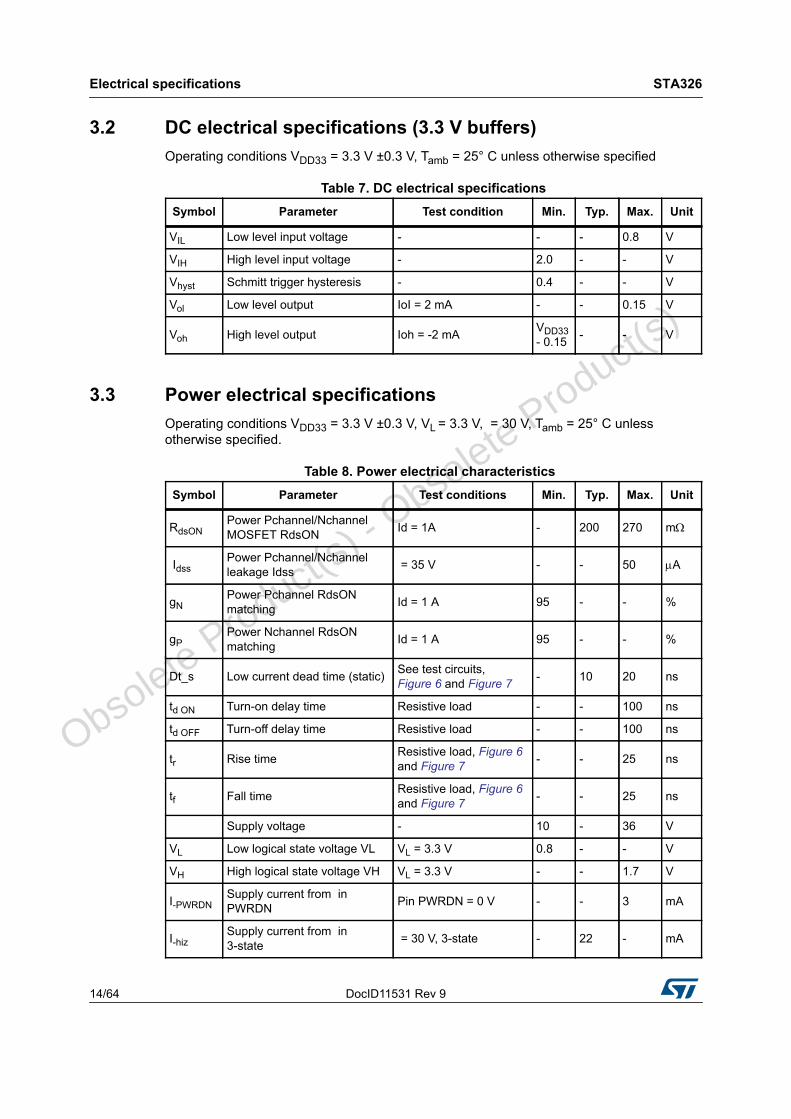
3.2 DC electrical specifications (3.3 V buffers)Operating conditions VDD33 = 3.3 V ±0.3 V, Tamb = 25° C unless otherwise specified
3.3 Power electrical specificationsOperating conditions VDD33 = 3.3 V ±0.3 V, VL = 3.3 V, = 30 V, Tamb = 25° C unless otherwise specified.
Table 7. DC electrical specificationsSymbol Parameter Test condition Min. Typ. Max. Unit
VIL Low level input voltage - - - 0.8 V
VIH High level input voltage - 2.0 - - V
Vhyst Schmitt trigger hysteresis - 0.4 - - V
Vol Low level output IoI = 2 mA - - 0.15 V
Voh High level output Ioh = -2 mA VDD33- 0.15 - - V
Table 8. Power electrical characteristics Symbol Parameter Test conditions Min. Typ. Max. Unit
RdsONPower Pchannel/Nchannel MOSFET RdsON Id = 1A - 200 270 m
IdssPower Pchannel/Nchannel leakage Idss = 35 V - - 50 A
gNPower Pchannel RdsON matching Id = 1 A 95 - - %
gPPower Nchannel RdsON matching Id = 1 A 95 - - %
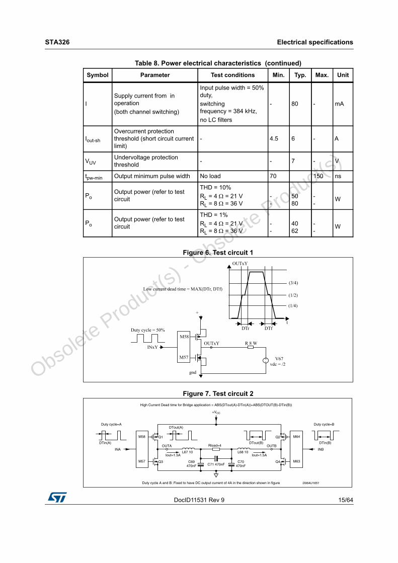
Dt_s Low current dead time (static) See test circuits, Figure 6 and Figure 7 - 10 20 ns
td ON Turn-on delay time Resistive load - - 100 ns
td OFF Turn-off delay time Resistive load - - 100 ns
tr Rise time Resistive load, Figure 6 and Figure 7 - - 25 ns
tf Fall time Resistive load, Figure 6 and Figure 7 - - 25 ns
Supply voltage - 10 - 36 V
VL Low logical state voltage VL VL = 3.3 V 0.8 - - V
VH High logical state voltage VH VL = 3.3 V - - 1.7 V
I-PWRDNSupply current from in PWRDN Pin PWRDN = 0 V - - 3 mA
I-hizSupply current from in 3-state = 30 V, 3-state - 22 - mA
O
bsolete Product(
s) - O
bsolete Product(
s)
DocID11531 Rev 9 15/64
STA326 Electrical specifications
64
Figure 6. Test circuit 1
Figure 7. Test circuit 2
ISupply current from in operation(both channel switching)
Input pulse width = 50% duty,switching frequency = 384 kHz,no LC filters
- 80 - mA
Iout-sh
Overcurrent protection threshold (short circuit current limit)
- 4.5 6 - A
VUVUndervoltage protection threshold - - 7 - V
tpw-min Output minimum pulse width No load 70 150 ns
PoOutput power (refer to test circuit
THD = 10%RL = 4 = 21 VRL = 8 = 36 V
--
5080
--
W
PoOutput power (refer to test circuit
THD = 1%RL = 4 = 21 VRL = 8 = 36 V
--
4062
--
W
Table 8. Power electrical characteristics (continued)Symbol Parameter Test conditions Min. Typ. Max. Unit
DTr DTf
(3/4)
(1/2)
(1/4)
t
OUTxY
Low current dead time = MAX(DTr, DTf)
+
Duty cycle = 50%
INxY
M58
M57
OUTxY
gnd
vdc = /2V67
R 8 W
+-
High Current Dead time for Bridge application = ABS(DTout(A)-DTin(A))+ABS(DTOUT(B)-DTin(B))
+VCC
Rload=4
Q2
OUTBDTout(B) DTin(B)
DTout(A)
C71 470nFC70
470nFC69
470nF
Iout=1.5AIout=1.5A
Q4
Q1
Q3
M64
INB
M63
D06AU1651
M58
INA
M57
DTin(A)
Duty cycle=A Duty cycle=B
Duty cycle A and B: Fixed to have DC output current of 4A in the direction shown in figure
L68 10L67 10
OUTA
O
bsolete Product(
s) - O
bsolete Product(
s)
Power supply and control sequencing STA326
16/64 DocID11531 Rev 9
4 Power supply and control sequencing
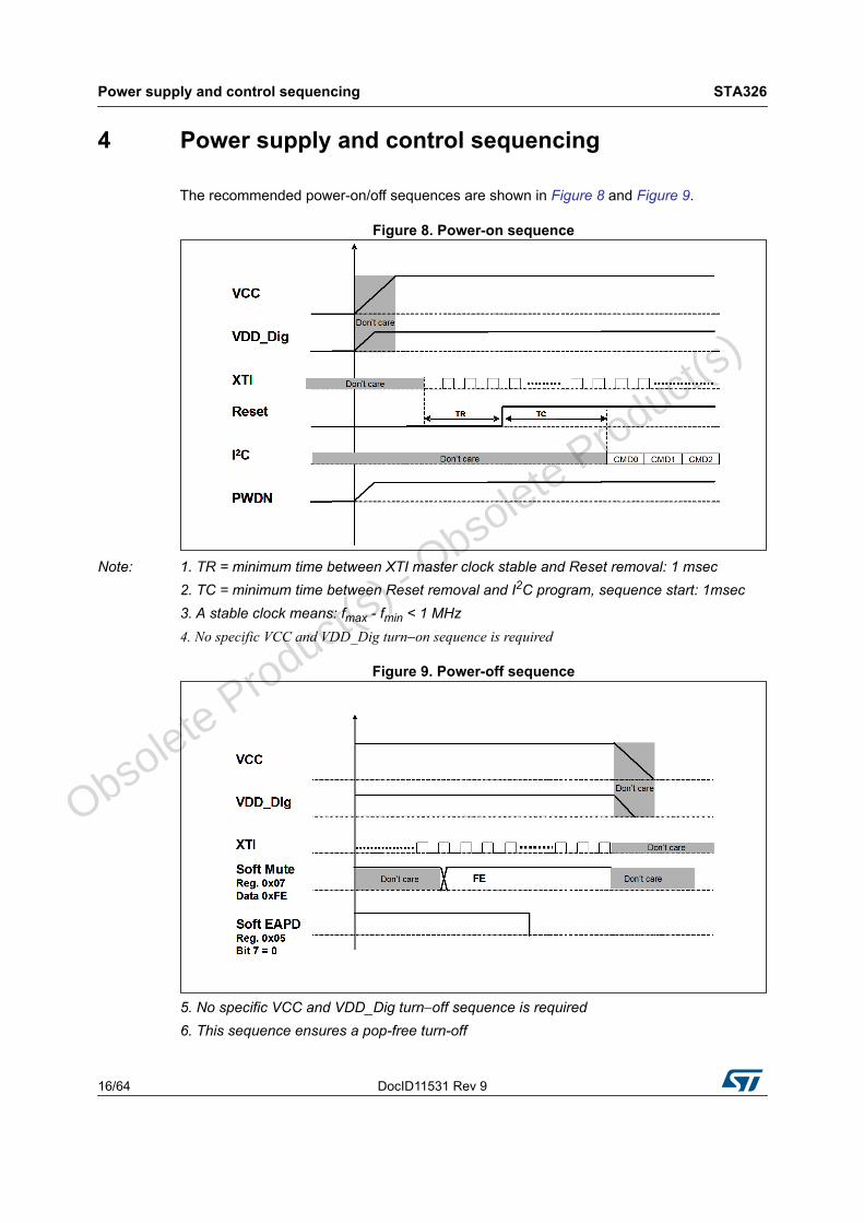
The recommended power-on/off sequences are shown in Figure 8 and Figure 9.
Figure 8. Power-on sequence
Note: 1. TR = minimum time between XTI master clock stable and Reset removal: 1 msec2. TC = minimum time between Reset removal and I2C program, sequence start: 1msec3. A stable clock means: fmax - fmin < 1 MHz4. No specific VCC and VDD_Dig turn−on sequence is required
Figure 9. Power-off sequence
5. No specific VCC and VDD_Dig turn−off sequence is required6. This sequence ensures a pop-free turn-off
O
bsolete Product(
s) - O
bsolete Product(
s)
DocID11531 Rev 9 17/64
STA326 Characterization curves
64
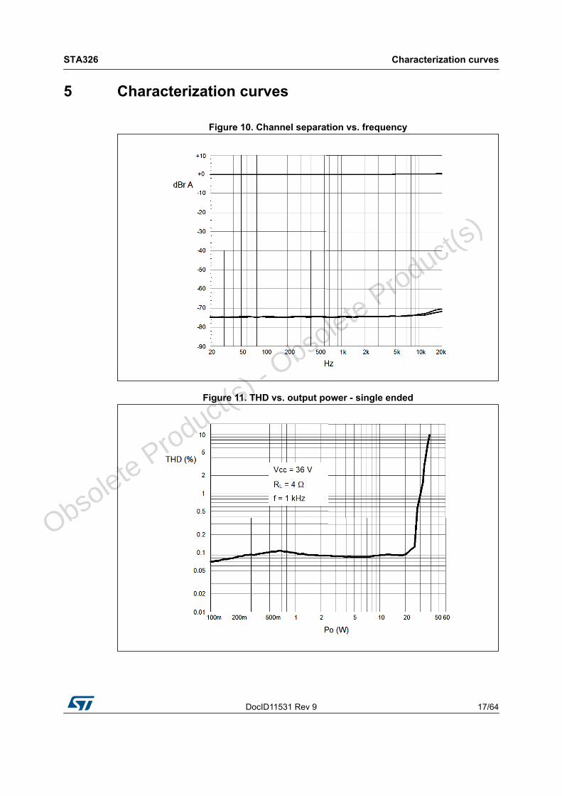
5 Characterization curves
Figure 10. Channel separation vs. frequency
Figure 11. THD vs. output power - single ended
O
bsolete Product(
s) - O
bsolete Product(
s)
Characterization curves STA326
18/64 DocID11531 Rev 9
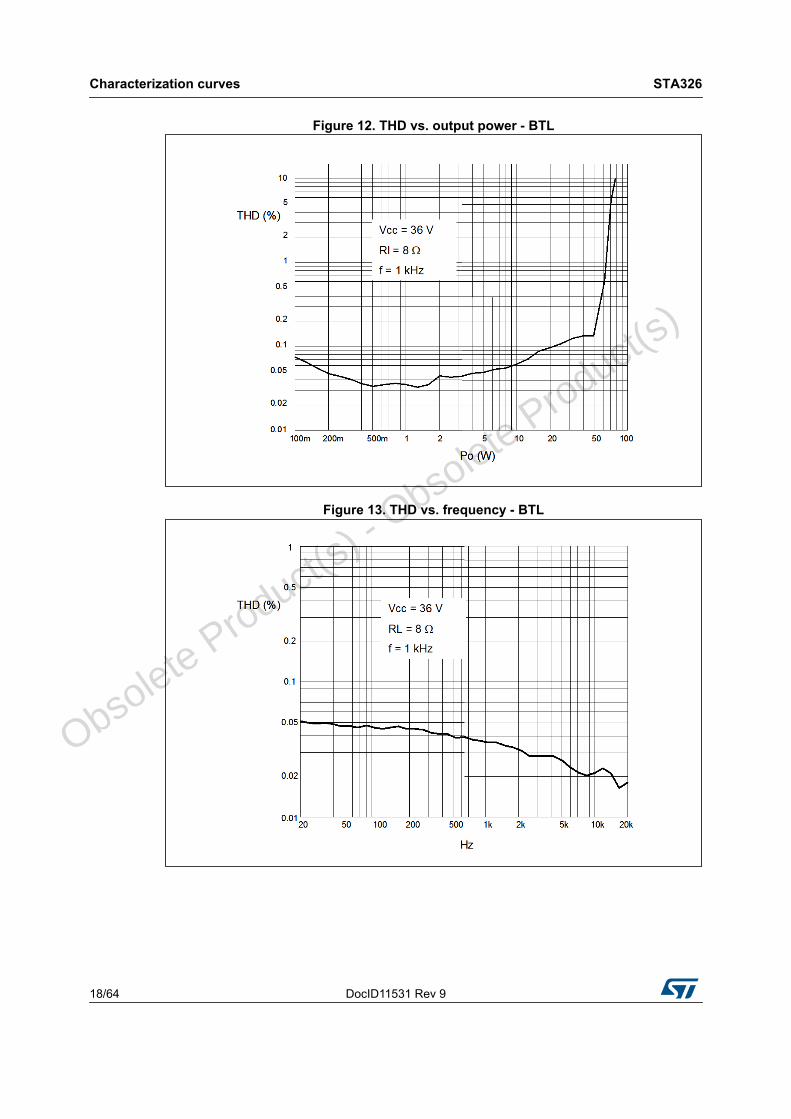
Figure 12. THD vs. output power - BTL
Figure 13. THD vs. frequency - BTL
O
bsolete Product(
s) - O
bsolete Product(
s)
DocID11531 Rev 9 19/64
STA326 I2C bus specification
64
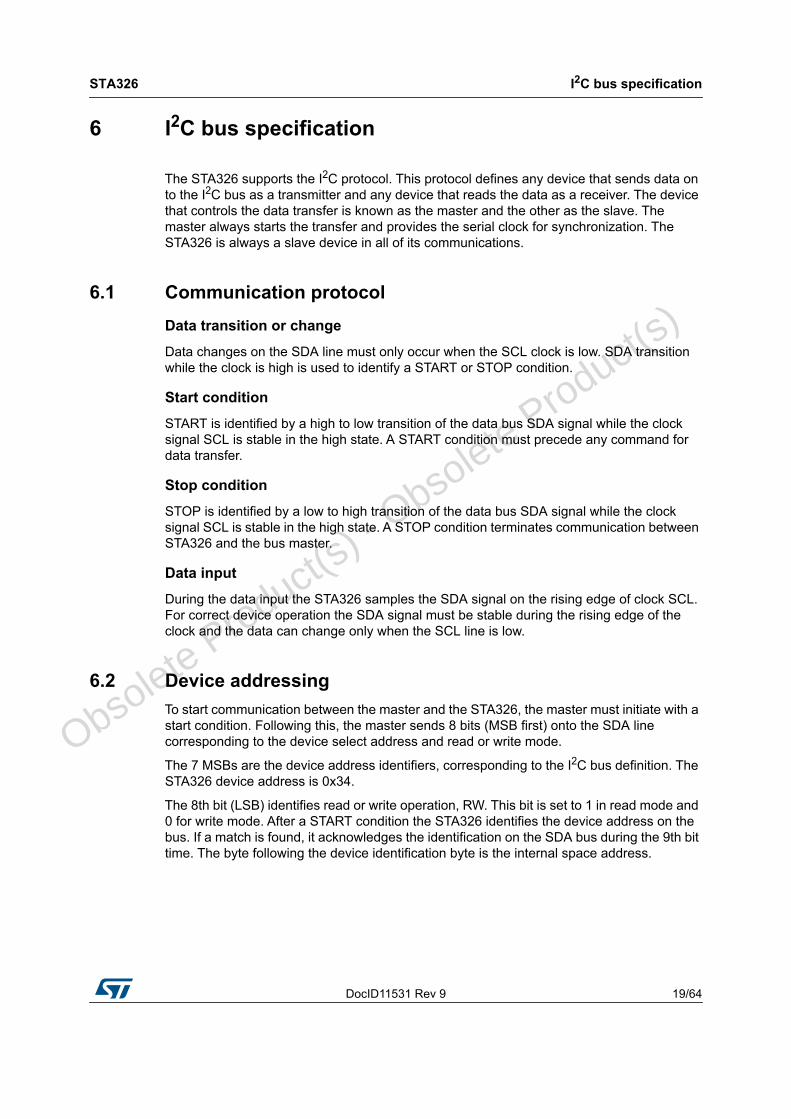
6 I2C bus specification
The STA326 supports the I2C protocol. This protocol defines any device that sends data on to the I2C bus as a transmitter and any device that reads the data as a receiver. The device that controls the data transfer is known as the master and the other as the slave. The master always starts the transfer and provides the serial clock for synchronization. The STA326 is always a slave device in all of its communications.
6.1 Communication protocolData transition or change
Data changes on the SDA line must only occur when the SCL clock is low. SDA transition while the clock is high is used to identify a START or STOP condition.
Start condition
START is identified by a high to low transition of the data bus SDA signal while the clock signal SCL is stable in the high state. A START condition must precede any command for data transfer.
Stop condition
STOP is identified by a low to high transition of the data bus SDA signal while the clock signal SCL is stable in the high state. A STOP condition terminates communication between STA326 and the bus master.
Data input
During the data input the STA326 samples the SDA signal on the rising edge of clock SCL. For correct device operation the SDA signal must be stable during the rising edge of the clock and the data can change only when the SCL line is low.
6.2 Device addressing To start communication between the master and the STA326, the master must initiate with a start condition. Following this, the master sends 8 bits (MSB first) onto the SDA line corresponding to the device select address and read or write mode.
The 7 MSBs are the device address identifiers, corresponding to the I2C bus definition. The STA326 device address is 0x34.
The 8th bit (LSB) identifies read or write operation, RW. This bit is set to 1 in read mode and 0 for write mode. After a START condition the STA326 identifies the device address on the bus. If a match is found, it acknowledges the identification on the SDA bus during the 9th bit time. The byte following the device identification byte is the internal space address.
O
bsolete Product(
s) - O
bsolete Product(
s)
I2C bus specification STA326
20/64 DocID11531 Rev 9
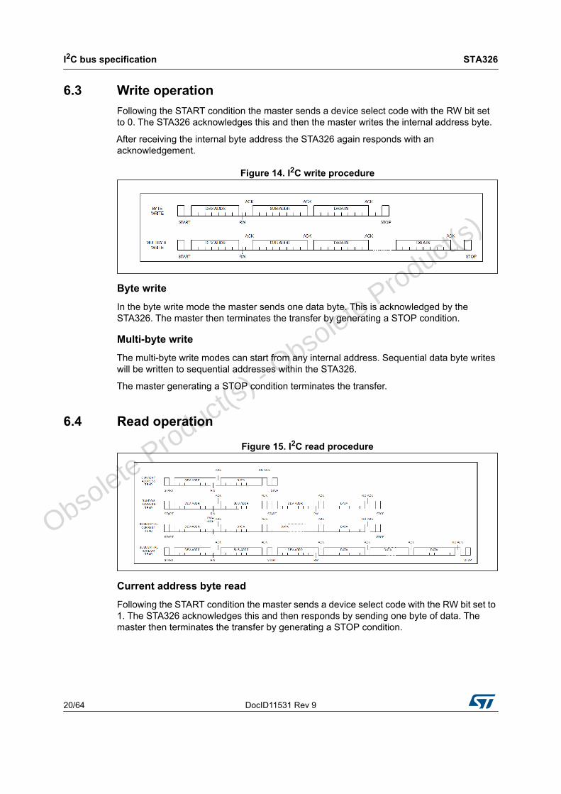
6.3 Write operationFollowing the START condition the master sends a device select code with the RW bit set to 0. The STA326 acknowledges this and then the master writes the internal address byte.
After receiving the internal byte address the STA326 again responds with an acknowledgement.
Figure 14. I2C write procedure
Byte write
In the byte write mode the master sends one data byte. This is acknowledged by the STA326. The master then terminates the transfer by generating a STOP condition.
Multi-byte write
The multi-byte write modes can start from any internal address. Sequential data byte writes will be written to sequential addresses within the STA326.
The master generating a STOP condition terminates the transfer.
6.4 Read operation
Figure 15. I2C read procedure
Current address byte read
Following the START condition the master sends a device select code with the RW bit set to 1. The STA326 acknowledges this and then responds by sending one byte of data. The master then terminates the transfer by generating a STOP condition.
O
bsolete Product(
s) - O
bsolete Product(
s)
DocID11531 Rev 9 21/64
STA326 I2C bus specification
64
Current address multi-byte read
The multi-byte read modes can start from any internal address. Sequential data bytes will be read from sequential addresses within the STA326. The master acknowledges each data byte read and then generates a STOP condition terminating the transfer.
Random address byte read
Following the START condition the master sends a device select code with the RW bit set to 0. The STA326 acknowledges this and then the master writes the internal address byte. After receiving, the internal byte address the STA326 again responds with an acknowledgement. The master then initiates another START condition and sends the device select code with the RW bit set to 1. The STA326 acknowledges this and then responds by sending one byte of data. The master then terminates the transfer by generating a STOP condition.
Random address multi-byte read
The multi-byte read modes could start from any internal address. Sequential data bytes will be read from sequential addresses within the STA326. The master acknowledges each data byte read and then generates a STOP condition terminating the transfer.
O
bsolete Product(
s) - O
bsolete Product(
s)
Register description STA326
22/64 DocID11531 Rev 9
7 Register description
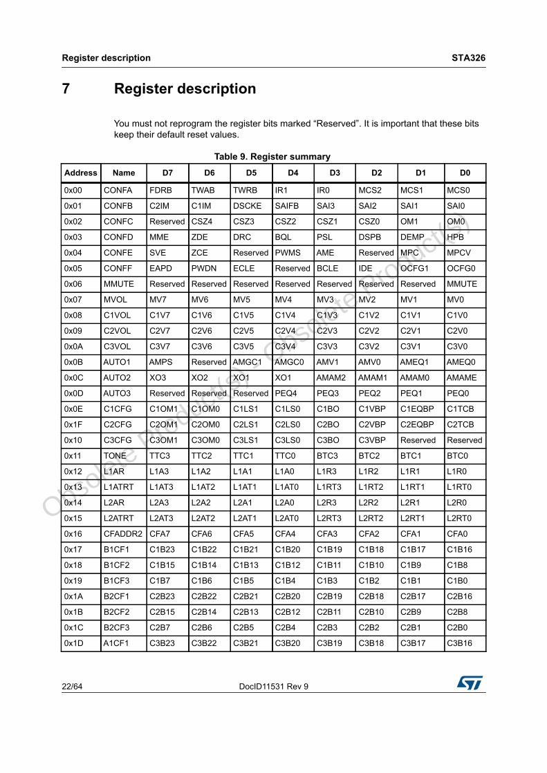
You must not reprogram the register bits marked “Reserved”. It is important that these bits keep their default reset values.
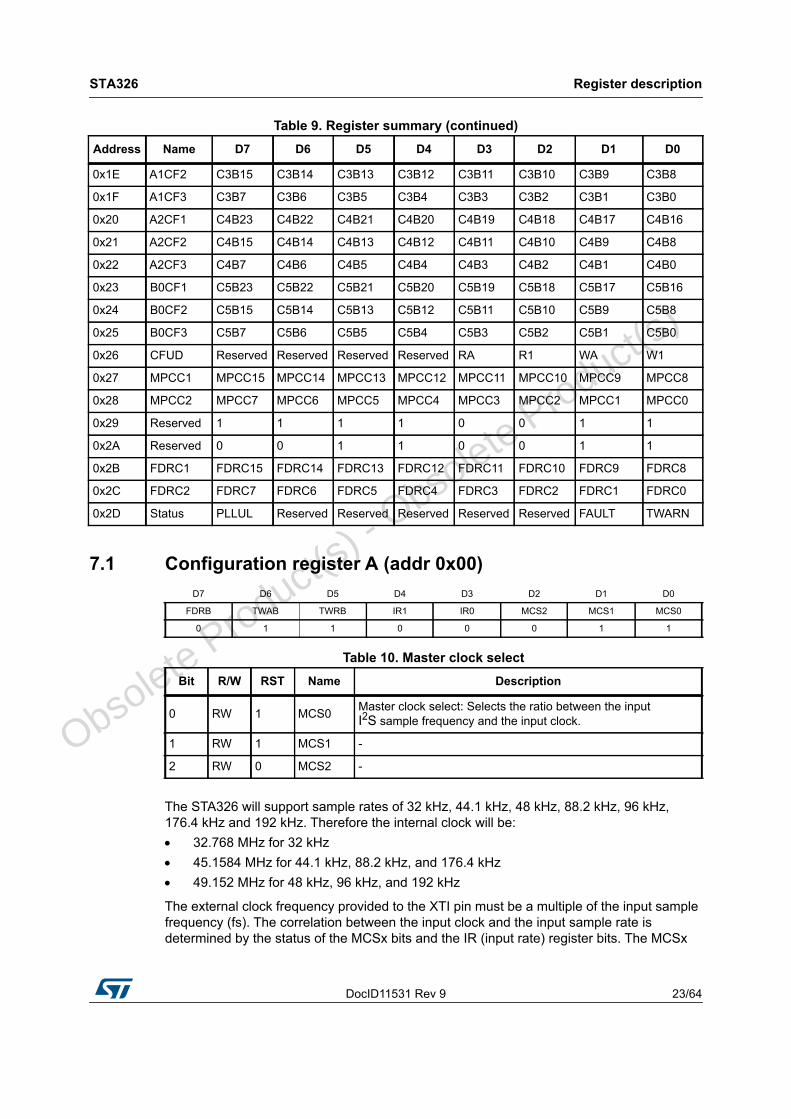
Table 9. Register summary Address Name D7 D6 D5 D4 D3 D2 D1 D0
0x00 CONFA FDRB TWAB TWRB IR1 IR0 MCS2 MCS1 MCS0
0x01 CONFB C2IM C1IM DSCKE SAIFB SAI3 SAI2 SAI1 SAI0
0x02 CONFC Reserved CSZ4 CSZ3 CSZ2 CSZ1 CSZ0 OM1 OM0
0x03 CONFD MME ZDE DRC BQL PSL DSPB DEMP HPB
0x04 CONFE SVE ZCE Reserved PWMS AME Reserved MPC MPCV
0x05 CONFF EAPD PWDN ECLE Reserved BCLE IDE OCFG1 OCFG0
0x06 MMUTE Reserved Reserved Reserved Reserved Reserved Reserved Reserved MMUTE
0x07 MVOL MV7 MV6 MV5 MV4 MV3 MV2 MV1 MV0
0x08 C1VOL C1V7 C1V6 C1V5 C1V4 C1V3 C1V2 C1V1 C1V0
0x09 C2VOL C2V7 C2V6 C2V5 C2V4 C2V3 C2V2 C2V1 C2V0
0x0A C3VOL C3V7 C3V6 C3V5 C3V4 C3V3 C3V2 C3V1 C3V0
0x0B AUTO1 AMPS Reserved AMGC1 AMGC0 AMV1 AMV0 AMEQ1 AMEQ0
0x0C AUTO2 XO3 XO2 XO1 XO1 AMAM2 AMAM1 AMAM0 AMAME
0x0D AUTO3 Reserved Reserved Reserved PEQ4 PEQ3 PEQ2 PEQ1 PEQ0
0x0E C1CFG C1OM1 C1OM0 C1LS1 C1LS0 C1BO C1VBP C1EQBP C1TCB
0x1F C2CFG C2OM1 C2OM0 C2LS1 C2LS0 C2BO C2VBP C2EQBP C2TCB
0x10 C3CFG C3OM1 C3OM0 C3LS1 C3LS0 C3BO C3VBP Reserved Reserved
0x11 TONE TTC3 TTC2 TTC1 TTC0 BTC3 BTC2 BTC1 BTC0
0x12 L1AR L1A3 L1A2 L1A1 L1A0 L1R3 L1R2 L1R1 L1R0
0x13 L1ATRT L1AT3 L1AT2 L1AT1 L1AT0 L1RT3 L1RT2 L1RT1 L1RT0
0x14 L2AR L2A3 L2A2 L2A1 L2A0 L2R3 L2R2 L2R1 L2R0
0x15 L2ATRT L2AT3 L2AT2 L2AT1 L2AT0 L2RT3 L2RT2 L2RT1 L2RT0
0x16 CFADDR2 CFA7 CFA6 CFA5 CFA4 CFA3 CFA2 CFA1 CFA0
0x17 B1CF1 C1B23 C1B22 C1B21 C1B20 C1B19 C1B18 C1B17 C1B16
0x18 B1CF2 C1B15 C1B14 C1B13 C1B12 C1B11 C1B10 C1B9 C1B8
0x19 B1CF3 C1B7 C1B6 C1B5 C1B4 C1B3 C1B2 C1B1 C1B0
0x1A B2CF1 C2B23 C2B22 C2B21 C2B20 C2B19 C2B18 C2B17 C2B16
0x1B B2CF2 C2B15 C2B14 C2B13 C2B12 C2B11 C2B10 C2B9 C2B8
0x1C B2CF3 C2B7 C2B6 C2B5 C2B4 C2B3 C2B2 C2B1 C2B0
0x1D A1CF1 C3B23 C3B22 C3B21 C3B20 C3B19 C3B18 C3B17 C3B16
O
bsolete Product(
s) - O
bsolete Product(
s)
DocID11531 Rev 9 23/64
STA326 Register description
64
7.1 Configuration register A (addr 0x00)
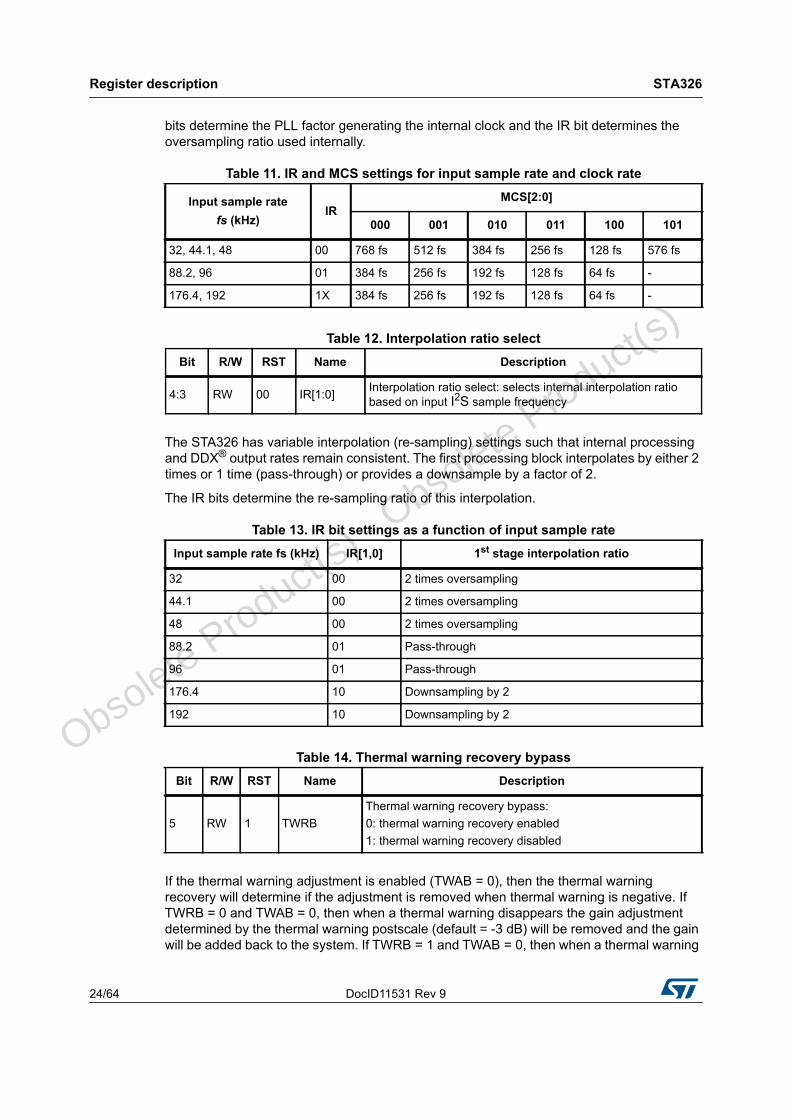
The STA326 will support sample rates of 32 kHz, 44.1 kHz, 48 kHz, 88.2 kHz, 96 kHz, 176.4 kHz and 192 kHz. Therefore the internal clock will be: 32.768 MHz for 32 kHz 45.1584 MHz for 44.1 kHz, 88.2 kHz, and 176.4 kHz 49.152 MHz for 48 kHz, 96 kHz, and 192 kHz
The external clock frequency provided to the XTI pin must be a multiple of the input sample frequency (fs). The correlation between the input clock and the input sample rate is determined by the status of the MCSx bits and the IR (input rate) register bits. The MCSx
0x1E A1CF2 C3B15 C3B14 C3B13 C3B12 C3B11 C3B10 C3B9 C3B8
0x1F A1CF3 C3B7 C3B6 C3B5 C3B4 C3B3 C3B2 C3B1 C3B0
0x20 A2CF1 C4B23 C4B22 C4B21 C4B20 C4B19 C4B18 C4B17 C4B16
0x21 A2CF2 C4B15 C4B14 C4B13 C4B12 C4B11 C4B10 C4B9 C4B8
0x22 A2CF3 C4B7 C4B6 C4B5 C4B4 C4B3 C4B2 C4B1 C4B0
0x23 B0CF1 C5B23 C5B22 C5B21 C5B20 C5B19 C5B18 C5B17 C5B16
0x24 B0CF2 C5B15 C5B14 C5B13 C5B12 C5B11 C5B10 C5B9 C5B8
0x25 B0CF3 C5B7 C5B6 C5B5 C5B4 C5B3 C5B2 C5B1 C5B0
0x26 CFUD Reserved Reserved Reserved Reserved RA R1 WA W1
0x27 MPCC1 MPCC15 MPCC14 MPCC13 MPCC12 MPCC11 MPCC10 MPCC9 MPCC8
0x28 MPCC2 MPCC7 MPCC6 MPCC5 MPCC4 MPCC3 MPCC2 MPCC1 MPCC0
0x29 Reserved 1 1 1 1 0 0 1 1
0x2A Reserved 0 0 1 1 0 0 1 1
0x2B FDRC1 FDRC15 FDRC14 FDRC13 FDRC12 FDRC11 FDRC10 FDRC9 FDRC8
0x2C FDRC2 FDRC7 FDRC6 FDRC5 FDRC4 FDRC3 FDRC2 FDRC1 FDRC0
0x2D Status PLLUL Reserved Reserved Reserved Reserved Reserved FAULT TWARN
D7 D6 D5 D4 D3 D2 D1 D0
FDRB TWAB TWRB IR1 IR0 MCS2 MCS1 MCS0
0 1 1 0 0 0 1 1
Table 9. Register summary (continued)Address Name D7 D6 D5 D4 D3 D2 D1 D0
Table 10. Master clock selectBit R/W RST Name Description
0 RW 1 MCS0 Master clock select: Selects the ratio between the input I2S sample frequency and the input clock.
1 RW 1 MCS1 -
2 RW 0 MCS2 - O
bsolete Product(
s) - O
bsolete Product(
s)
Register description STA326
24/64 DocID11531 Rev 9
bits determine the PLL factor generating the internal clock and the IR bit determines the oversampling ratio used internally.
The STA326 has variable interpolation (re-sampling) settings such that internal processing and DDX® output rates remain consistent. The first processing block interpolates by either 2 times or 1 time (pass-through) or provides a downsample by a factor of 2.
The IR bits determine the re-sampling ratio of this interpolation.
If the thermal warning adjustment is enabled (TWAB = 0), then the thermal warning recovery will determine if the adjustment is removed when thermal warning is negative. If TWRB = 0 and TWAB = 0, then when a thermal warning disappears the gain adjustment determined by the thermal warning postscale (default = -3 dB) will be removed and the gain will be added back to the system. If TWRB = 1 and TWAB = 0, then when a thermal warning
Table 11. IR and MCS settings for input sample rate and clock rate
Input sample rate fs (kHz)
IRMCS[2:0]
000 001 010 011 100 101
32, 44.1, 48 00 768 fs 512 fs 384 fs 256 fs 128 fs 576 fs
88.2, 96 01 384 fs 256 fs 192 fs 128 fs 64 fs -
176.4, 192 1X 384 fs 256 fs 192 fs 128 fs 64 fs -
Table 12. Interpolation ratio selectBit R/W RST Name Description
4:3 RW 00 IR[1:0] Interpolation ratio select: selects internal interpolation ratio based on input I2S sample frequency
Table 13. IR bit settings as a function of input sample rateInput sample rate fs (kHz) IR[1,0] 1st stage interpolation ratio
32 00 2 times oversampling
44.1 00 2 times oversampling
48 00 2 times oversampling
88.2 01 Pass-through
96 01 Pass-through
176.4 10 Downsampling by 2
192 10 Downsampling by 2
Table 14. Thermal warning recovery bypassBit R/W RST Name Description
5 RW 1 TWRBThermal warning recovery bypass:0: thermal warning recovery enabled1: thermal warning recovery disabled
O
bsolete Product(
s) - O
bsolete Product(
s)
DocID11531 Rev 9 25/64
STA326 Register description
64
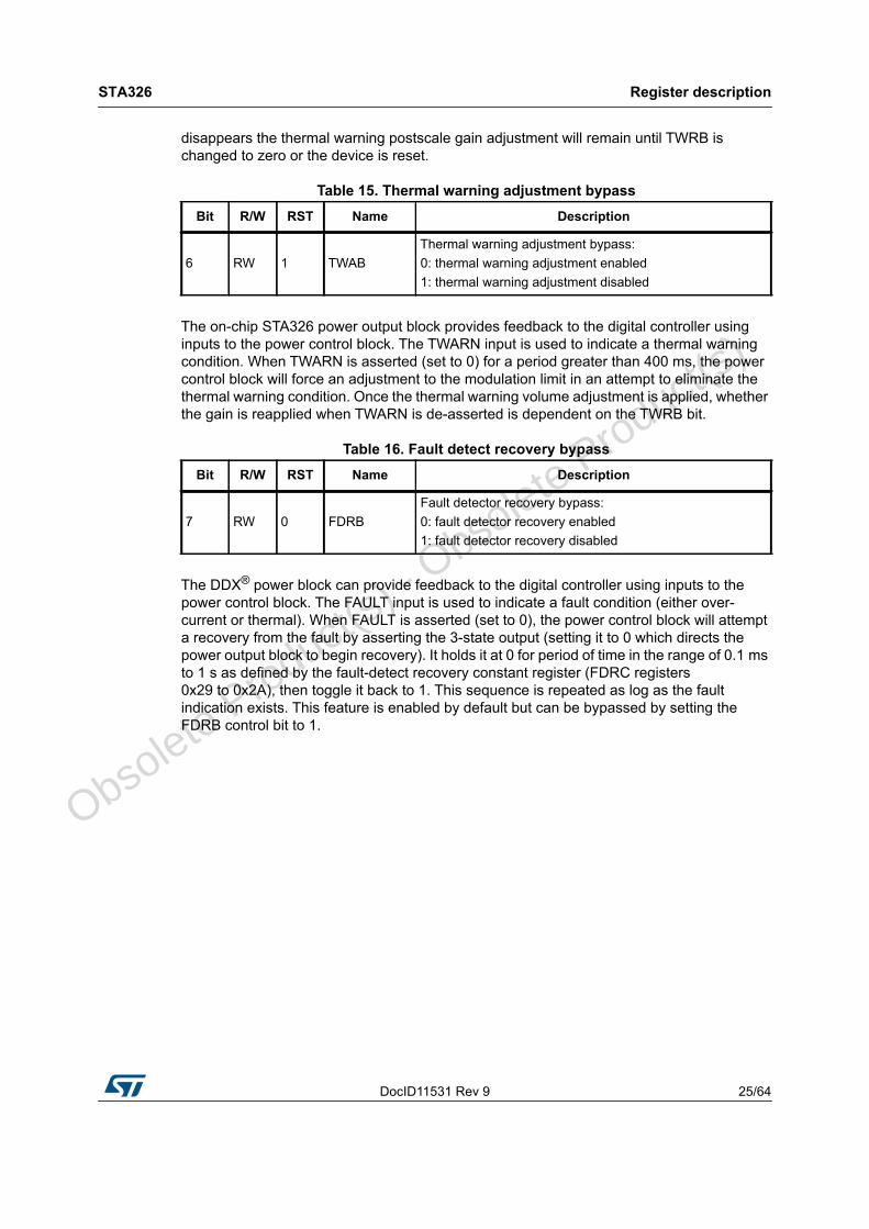
disappears the thermal warning postscale gain adjustment will remain until TWRB is changed to zero or the device is reset.
The on-chip STA326 power output block provides feedback to the digital controller using inputs to the power control block. The TWARN input is used to indicate a thermal warning condition. When TWARN is asserted (set to 0) for a period greater than 400 ms, the power control block will force an adjustment to the modulation limit in an attempt to eliminate the thermal warning condition. Once the thermal warning volume adjustment is applied, whether the gain is reapplied when TWARN is de-asserted is dependent on the TWRB bit.
The DDX® power block can provide feedback to the digital controller using inputs to the power control block. The FAULT input is used to indicate a fault condition (either over-current or thermal). When FAULT is asserted (set to 0), the power control block will attempt a recovery from the fault by asserting the 3-state output (setting it to 0 which directs the power output block to begin recovery). It holds it at 0 for period of time in the range of 0.1 ms to 1 s as defined by the fault-detect recovery constant register (FDRC registers 0x29 to 0x2A), then toggle it back to 1. This sequence is repeated as log as the fault indication exists. This feature is enabled by default but can be bypassed by setting the FDRB control bit to 1.
Table 15. Thermal warning adjustment bypassBit R/W RST Name Description
6 RW 1 TWABThermal warning adjustment bypass:0: thermal warning adjustment enabled1: thermal warning adjustment disabled
Table 16. Fault detect recovery bypassBit R/W RST Name Description
7 RW 0 FDRBFault detector recovery bypass:0: fault detector recovery enabled1: fault detector recovery disabled
O
bsolete Product(
s) - O
bsolete Product(
s)
Register description STA326
26/64 DocID11531 Rev 9
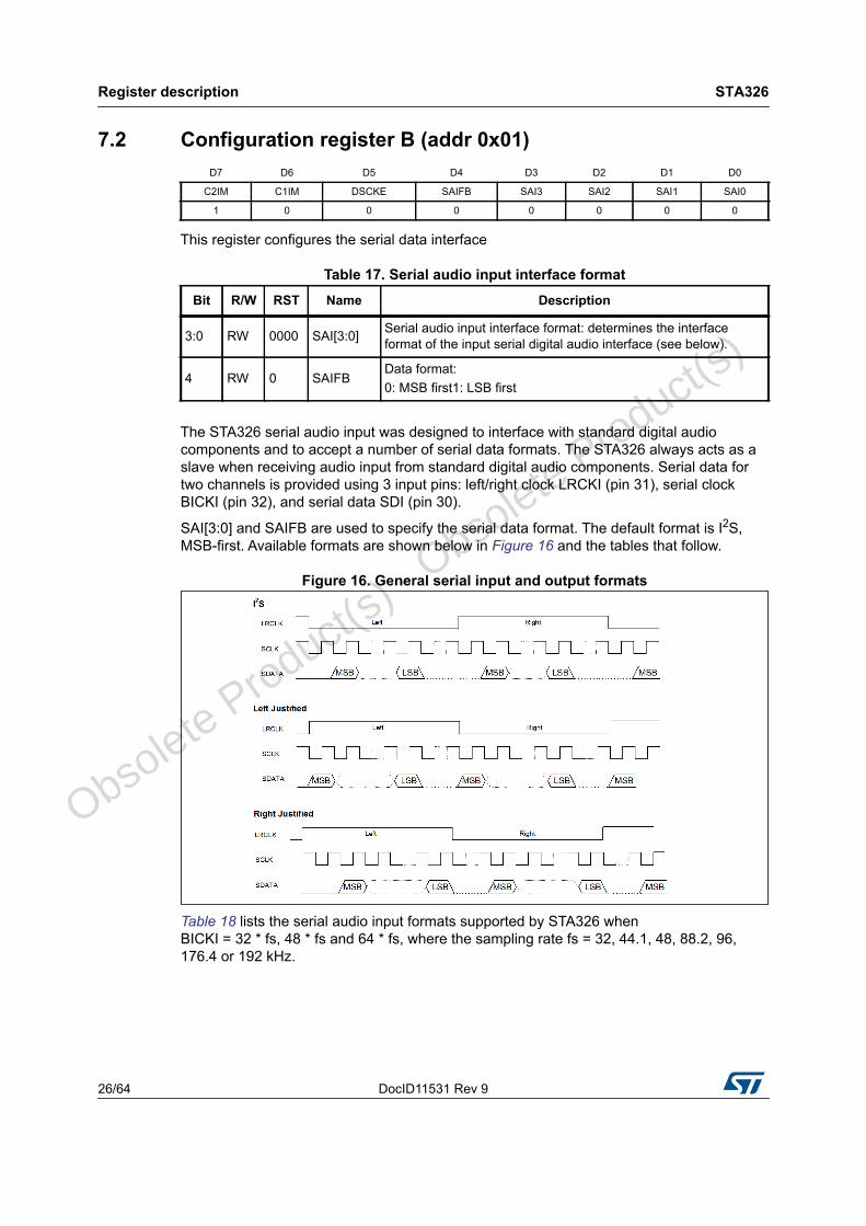
7.2 Configuration register B (addr 0x01)
This register configures the serial data interface
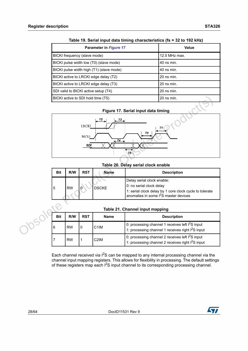
The STA326 serial audio input was designed to interface with standard digital audio components and to accept a number of serial data formats. The STA326 always acts as a slave when receiving audio input from standard digital audio components. Serial data for two channels is provided using 3 input pins: left/right clock LRCKI (pin 31), serial clock BICKI (pin 32), and serial data SDI (pin 30).
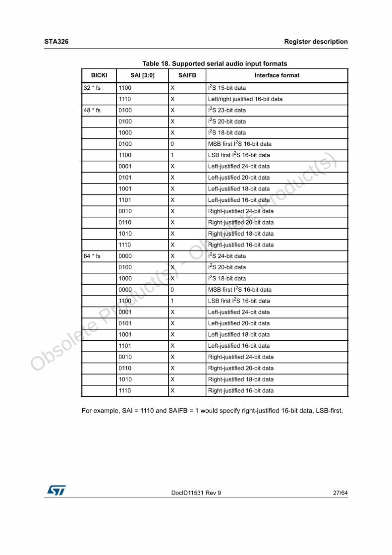
SAI[3:0] and SAIFB are used to specify the serial data format. The default format is I2S, MSB-first. Available formats are shown below in Figure 16 and the tables that follow.
Figure 16. General serial input and output formats
Table 18 lists the serial audio input formats supported by STA326 when BICKI = 32 * fs, 48 * fs and 64 * fs, where the sampling rate fs = 32, 44.1, 48, 88.2, 96, 176.4 or 192 kHz.
D7 D6 D5 D4 D3 D2 D1 D0
C2IM C1IM DSCKE SAIFB SAI3 SAI2 SAI1 SAI0
1 0 0 0 0 0 0 0
Table 17. Serial audio input interface formatBit R/W RST Name Description
3:0 RW 0000 SAI[3:0] Serial audio input interface format: determines the interface format of the input serial digital audio interface (see below).
4 RW 0 SAIFBData format:0: MSB first1: LSB first
O
bsolete Product(
s) - O
bsolete Product(
s)
DocID11531 Rev 9 27/64
STA326 Register description
64
For example, SAI = 1110 and SAIFB = 1 would specify right-justified 16-bit data, LSB-first.
Table 18. Supported serial audio input formatsBICKI SAI [3:0] SAIFB Interface format
32 * fs 1100 X I2S 15-bit data
1110 X Left/right justified 16-bit data
48 * fs 0100 X I2S 23-bit data
0100 X I2S 20-bit data
1000 X I2S 18-bit data
0100 0 MSB first I2S 16-bit data
1100 1 LSB first I2S 16-bit data
0001 X Left-justified 24-bit data
0101 X Left-justified 20-bit data
1001 X Left-justified 18-bit data
1101 X Left-justified 16-bit data
0010 X Right-justified 24-bit data
0110 X Right-justified 20-bit data
1010 X Right-justified 18-bit data
1110 X Right-justified 16-bit data
64 * fs 0000 X I2S 24-bit data
0100 X I2S 20-bit data
1000 X I2S 18-bit data
0000 0 MSB first I2S 16-bit data
1100 1 LSB first I2S 16-bit data
0001 X Left-justified 24-bit data
0101 X Left-justified 20-bit data
1001 X Left-justified 18-bit data
1101 X Left-justified 16-bit data
0010 X Right-justified 24-bit data
0110 X Right-justified 20-bit data
1010 X Right-justified 18-bit data
1110 X Right-justified 16-bit data O
bsolete Product(
s) - O
bsolete Product(
s)
Register description STA326
28/64 DocID11531 Rev 9
Figure 17. Serial input data timing
Each channel received via I2S can be mapped to any internal processing channel via the channel input mapping registers. This allows for flexibility in processing. The default settings of these registers map each I2S input channel to its corresponding processing channel.
Table 19. Serial input data timing characteristics (fs = 32 to 192 kHz)Parameter in Figure 17 Value
BICKI frequency (slave mode) 12.5 MHz max.
BICKI pulse width low (T0) (slave mode) 40 ns min.
BICKI pulse width high (T1) (slave mode) 40 ns min.
BICKI active to LRCKI edge delay (T2) 20 ns min.
BICKI active to LRCKI edge delay (T3) 20 ns min.
SDI valid to BICKI active setup (T4) 20 ns min.
BICKI active to SDI hold time (T5) 20 ns min.
Table 20. Delay serial clock enableBit R/W RST Name Description
5 RW 0 DSCKE
Delay serial clock enable:0: no serial clock delay 1: serial clock delay by 1 core clock cycle to tolerate anomalies in some I2S master devices
Table 21. Channel input mappingBit R/W RST Name Description
6 RW 0 C1IM0: processing channel 1 receives left I2S input1: processing channel 1 receives right I2S input
7 RW 1 C2IM0: processing channel 2 receives left I2S input1: processing channel 2 receives right I2S input
Obso
lete Product(s)
- Obso
lete Product(s)
DocID11531 Rev 9 29/64
STA326 Register description
64
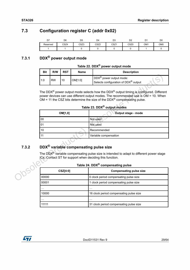
7.3 Configuration register C (addr 0x02)
7.3.1 DDX® power output mode
The DDX® power output mode selects how the DDX® output timing is configured. Different power devices can use different output modes. The recommended use is OM = 10. When OM = 11 the CSZ bits determine the size of the DDX® compensating pulse.
7.3.2 DDX® variable compensating pulse sizeThe DDX® variable compensating pulse size is intended to adapt to different power stage ICs. Contact ST for support when deciding this function.
D7 D6 D5 D4 D3 D2 D1 D0
Reserved CSZ4 CSZ3 CSZ2 CSZ1 CSZ0 OM1 OM0
1 1 0 0 0 0 1 0
Table 22. DDX® power output modeBit R/W RST Name Description
1:0 RW 10 OM[1:0]DDX® power output mode:Selects configuration of DDX® output
Table 23. DDX® output modesOM[1,0] Output stage - mode
00 Not used
01 Not used
10 Recommended
11 Variable compensation
Table 24. DDX® compensating pulseCSZ[4:0] Compensating pulse size
00000 0 clock period compensating pulse size
00001 1 clock period compensating pulse size
… …
10000 16 clock period compensating pulse size
… …
11111 31 clock period compensating pulse size
O
bsolete Product(
s) - O
bsolete Product(
s)
Register description STA326
30/64 DocID11531 Rev 9
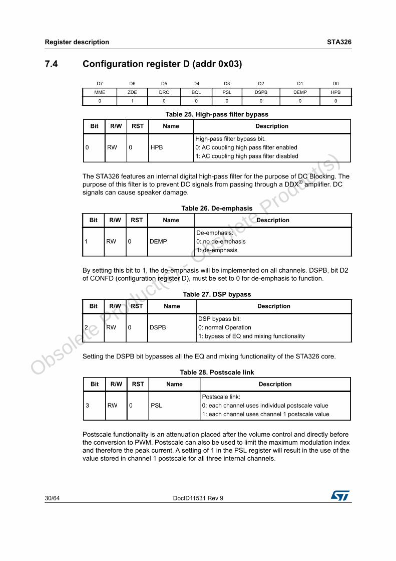
7.4 Configuration register D (addr 0x03)
The STA326 features an internal digital high-pass filter for the purpose of DC Blocking. The purpose of this filter is to prevent DC signals from passing through a DDX® amplifier. DC signals can cause speaker damage.
By setting this bit to 1, the de-emphasis will be implemented on all channels. DSPB, bit D2 of CONFD (configuration register D), must be set to 0 for de-emphasis to function.
Setting the DSPB bit bypasses all the EQ and mixing functionality of the STA326 core.
Postscale functionality is an attenuation placed after the volume control and directly before the conversion to PWM. Postscale can also be used to limit the maximum modulation index and therefore the peak current. A setting of 1 in the PSL register will result in the use of the value stored in channel 1 postscale for all three internal channels.
D7 D6 D5 D4 D3 D2 D1 D0
MME ZDE DRC BQL PSL DSPB DEMP HPB
0 1 0 0 0 0 0 0
Table 25. High-pass filter bypassBit R/W RST Name Description
0 RW 0 HPBHigh-pass filter bypass bit.0: AC coupling high pass filter enabled1: AC coupling high pass filter disabled
Table 26. De-emphasisBit R/W RST Name Description
1 RW 0 DEMPDe-emphasis:0: no de-emphasis1: de-emphasis
Table 27. DSP bypassBit R/W RST Name Description
2 RW 0 DSPBDSP bypass bit:0: normal Operation1: bypass of EQ and mixing functionality
Table 28. Postscale linkBit R/W RST Name Description
3 RW 0 PSLPostscale link:0: each channel uses individual postscale value 1: each channel uses channel 1 postscale value
O
bsolete Product(
s) - O
bsolete Product(
s)
DocID11531 Rev 9 31/64
STA326 Register description
64
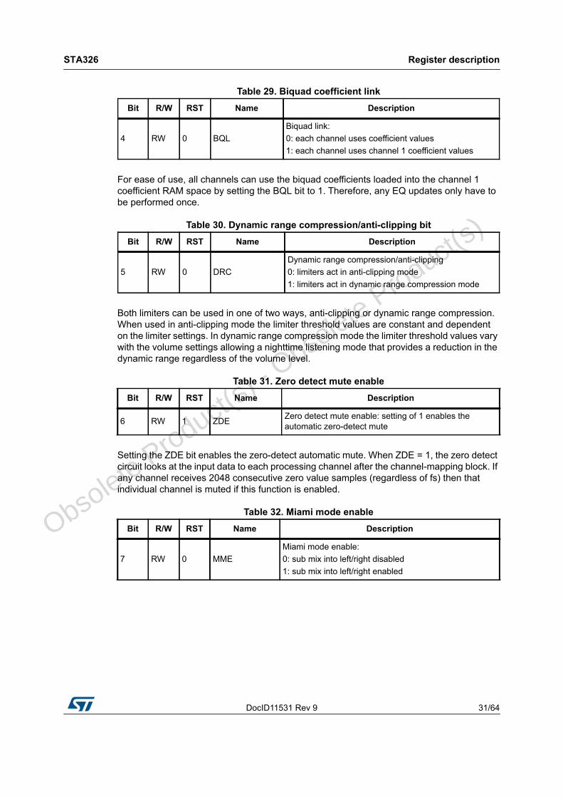
For ease of use, all channels can use the biquad coefficients loaded into the channel 1 coefficient RAM space by setting the BQL bit to 1. Therefore, any EQ updates only have to be performed once.
Both limiters can be used in one of two ways, anti-clipping or dynamic range compression. When used in anti-clipping mode the limiter threshold values are constant and dependent on the limiter settings. In dynamic range compression mode the limiter threshold values vary with the volume settings allowing a nighttime listening mode that provides a reduction in the dynamic range regardless of the volume level.
Setting the ZDE bit enables the zero-detect automatic mute. When ZDE = 1, the zero detect circuit looks at the input data to each processing channel after the channel-mapping block. If any channel receives 2048 consecutive zero value samples (regardless of fs) then that individual channel is muted if this function is enabled.
Table 29. Biquad coefficient linkBit R/W RST Name Description
4 RW 0 BQLBiquad link:0: each channel uses coefficient values 1: each channel uses channel 1 coefficient values
Table 30. Dynamic range compression/anti-clipping bitBit R/W RST Name Description
5 RW 0 DRCDynamic range compression/anti-clipping0: limiters act in anti-clipping mode1: limiters act in dynamic range compression mode
Table 31. Zero detect mute enableBit R/W RST Name Description
6 RW 1 ZDE Zero detect mute enable: setting of 1 enables the automatic zero-detect mute
Table 32. Miami mode enableBit R/W RST Name Description
7 RW 0 MMEMiami mode enable:0: sub mix into left/right disabled1: sub mix into left/right enabled
O
bsolete Product(
s) - O
bsolete Product(
s)
Register description STA326
32/64 DocID11531 Rev 9
7.5 Configuration register E (addr 0x04)
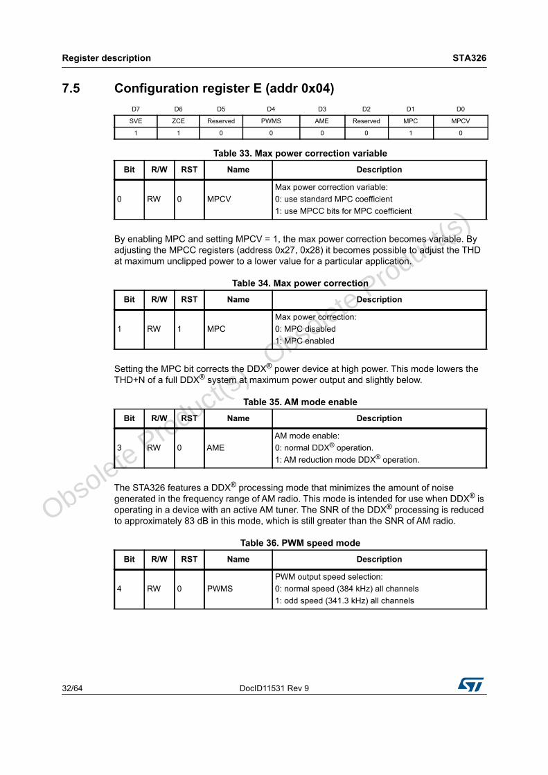
By enabling MPC and setting MPCV = 1, the max power correction becomes variable. By adjusting the MPCC registers (address 0x27, 0x28) it becomes possible to adjust the THD at maximum unclipped power to a lower value for a particular application.
Setting the MPC bit corrects the DDX® power device at high power. This mode lowers the THD+N of a full DDX® system at maximum power output and slightly below.
The STA326 features a DDX® processing mode that minimizes the amount of noise generated in the frequency range of AM radio. This mode is intended for use when DDX® is operating in a device with an active AM tuner. The SNR of the DDX® processing is reduced to approximately 83 dB in this mode, which is still greater than the SNR of AM radio.
D7 D6 D5 D4 D3 D2 D1 D0
SVE ZCE Reserved PWMS AME Reserved MPC MPCV
1 1 0 0 0 0 1 0
Table 33. Max power correction variableBit R/W RST Name Description
0 RW 0 MPCVMax power correction variable:0: use standard MPC coefficient1: use MPCC bits for MPC coefficient
Table 34. Max power correctionBit R/W RST Name Description
1 RW 1 MPCMax power correction:0: MPC disabled1: MPC enabled
Table 35. AM mode enableBit R/W RST Name Description
3 RW 0 AMEAM mode enable:0: normal DDX® operation.1: AM reduction mode DDX® operation.
Table 36. PWM speed modeBit R/W RST Name Description
4 RW 0 PWMSPWM output speed selection:0: normal speed (384 kHz) all channels1: odd speed (341.3 kHz) all channels
O
bsolete Product(
s) - O
bsolete Product(
s)
DocID11531 Rev 9 33/64
STA326 Register description
64
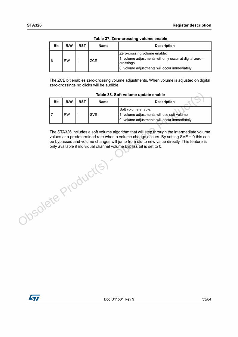
The ZCE bit enables zero-crossing volume adjustments. When volume is adjusted on digital zero-crossings no clicks will be audible.
The STA326 includes a soft volume algorithm that will step through the intermediate volume values at a predetermined rate when a volume change occurs. By setting SVE = 0 this can be bypassed and volume changes will jump from old to new value directly. This feature is only available if individual channel volume bypass bit is set to 0.
Table 37. Zero-crossing volume enableBit R/W RST Name Description
6 RW 1 ZCE
Zero-crossing volume enable:1: volume adjustments will only occur at digital zero-crossings0: volume adjustments will occur immediately
Table 38. Soft volume update enableBit R/W RST Name Description
7 RW 1 SVESoft volume enable:1: volume adjustments will use soft volume0: volume adjustments will occur immediately
O
bsolete Product(
s) - O
bsolete Product(
s)
Register description STA326
34/64 DocID11531 Rev 9
7.6 Configuration register F (addr 0x05)
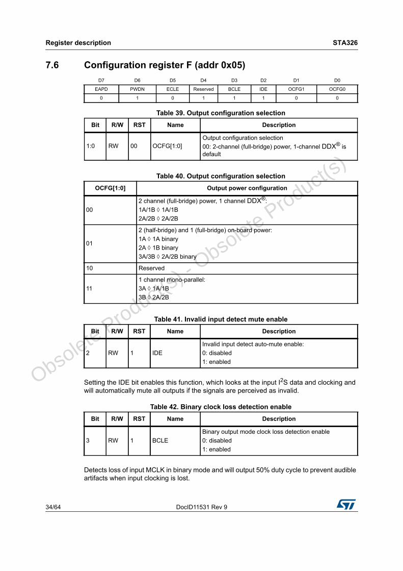
Setting the IDE bit enables this function, which looks at the input I2S data and clocking and will automatically mute all outputs if the signals are perceived as invalid.
Detects loss of input MCLK in binary mode and will output 50% duty cycle to prevent audible artifacts when input clocking is lost.
D7 D6 D5 D4 D3 D2 D1 D0
EAPD PWDN ECLE Reserved BCLE IDE OCFG1 OCFG0
0 1 0 1 1 1 0 0
Table 39. Output configuration selectionBit R/W RST Name Description
1:0 RW 00 OCFG[1:0]Output configuration selection00: 2-channel (full-bridge) power, 1-channel DDX® is default
Table 40. Output configuration selectionOCFG[1:0] Output power configuration
002 channel (full-bridge) power, 1 channel DDX®:1A/1B 1A/1B2A/2B 2A/2B
01
2 (half-bridge) and 1 (full-bridge) on-board power:1A 1A binary2A 1B binary3A/3B 2A/2B binary
10 Reserved
111 channel mono-parallel:3A 1A/1B 3B 2A/2B
Table 41. Invalid input detect mute enableBit R/W RST Name Description
2 RW 1 IDEInvalid input detect auto-mute enable:0: disabled1: enabled
Table 42. Binary clock loss detection enableBit R/W RST Name Description
3 RW 1 BCLEBinary output mode clock loss detection enable0: disabled1: enabled
O
bsolete Product(
s) - O
bsolete Product(
s)
DocID11531 Rev 9 35/64
STA326 Register description
64
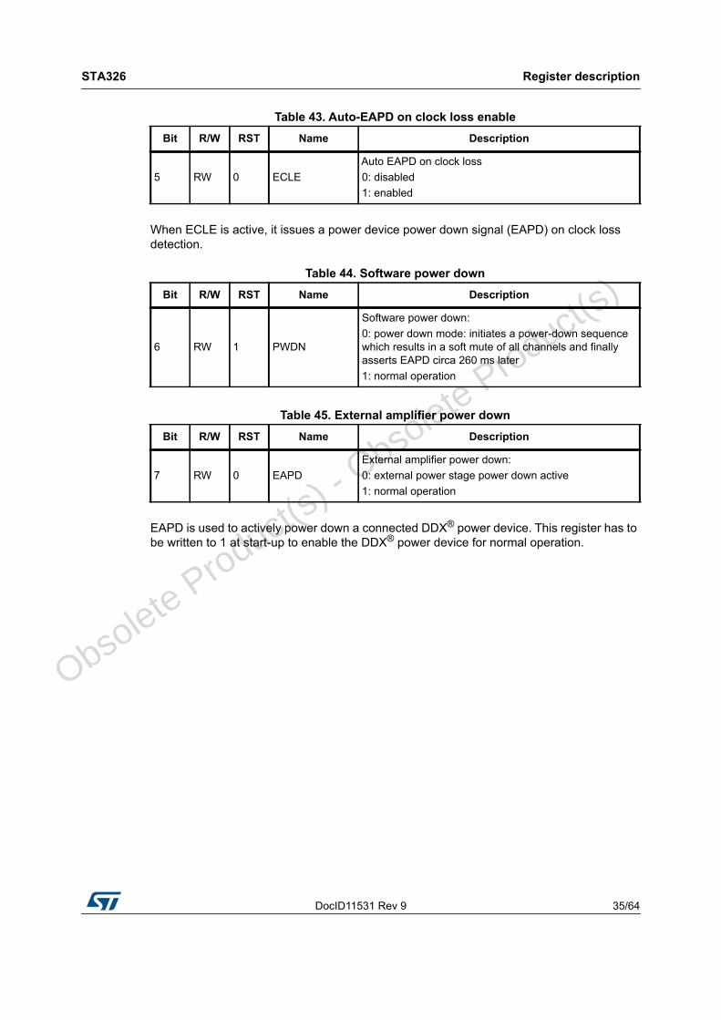
When ECLE is active, it issues a power device power down signal (EAPD) on clock loss detection.
EAPD is used to actively power down a connected DDX® power device. This register has to be written to 1 at start-up to enable the DDX® power device for normal operation.
Table 43. Auto-EAPD on clock loss enableBit R/W RST Name Description
5 RW 0 ECLEAuto EAPD on clock loss0: disabled1: enabled
Table 44. Software power downBit R/W RST Name Description
6 RW 1 PWDN
Software power down:0: power down mode: initiates a power-down sequence which results in a soft mute of all channels and finally asserts EAPD circa 260 ms later1: normal operation
Table 45. External amplifier power downBit R/W RST Name Description
7 RW 0 EAPDExternal amplifier power down:0: external power stage power down active1: normal operation
O
bsolete Product(
s) - O
bsolete Product(
s)
Register description STA326
36/64 DocID11531 Rev 9
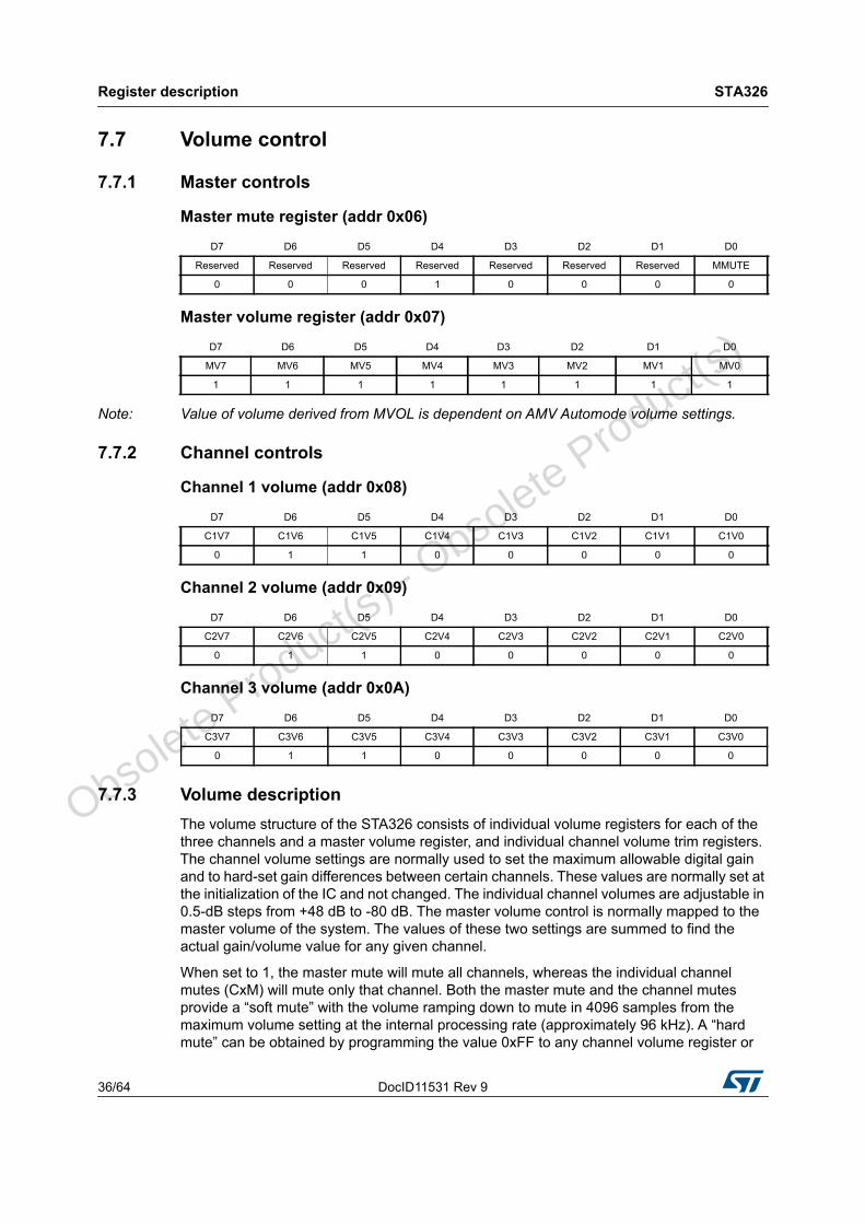
7.7 Volume control
7.7.1 Master controls
Master mute register (addr 0x06)
Master volume register (addr 0x07)
Note: Value of volume derived from MVOL is dependent on AMV Automode volume settings.
7.7.2 Channel controls
Channel 1 volume (addr 0x08)
Channel 2 volume (addr 0x09)
Channel 3 volume (addr 0x0A)
7.7.3 Volume descriptionThe volume structure of the STA326 consists of individual volume registers for each of the three channels and a master volume register, and individual channel volume trim registers. The channel volume settings are normally used to set the maximum allowable digital gain and to hard-set gain differences between certain channels. These values are normally set at the initialization of the IC and not changed. The individual channel volumes are adjustable in 0.5-dB steps from +48 dB to -80 dB. The master volume control is normally mapped to the master volume of the system. The values of these two settings are summed to find the actual gain/volume value for any given channel.
When set to 1, the master mute will mute all channels, whereas the individual channel mutes (CxM) will mute only that channel. Both the master mute and the channel mutes provide a “soft mute” with the volume ramping down to mute in 4096 samples from the maximum volume setting at the internal processing rate (approximately 96 kHz). A “hard mute” can be obtained by programming the value 0xFF to any channel volume register or
D7 D6 D5 D4 D3 D2 D1 D0
Reserved Reserved Reserved Reserved Reserved Reserved Reserved MMUTE
0 0 0 1 0 0 0 0
D7 D6 D5 D4 D3 D2 D1 D0
MV7 MV6 MV5 MV4 MV3 MV2 MV1 MV0
1 1 1 1 1 1 1 1
D7 D6 D5 D4 D3 D2 D1 D0
C1V7 C1V6 C1V5 C1V4 C1V3 C1V2 C1V1 C1V0
0 1 1 0 0 0 0 0
D7 D6 D5 D4 D3 D2 D1 D0
C2V7 C2V6 C2V5 C2V4 C2V3 C2V2 C2V1 C2V0
0 1 1 0 0 0 0 0
D7 D6 D5 D4 D3 D2 D1 D0
C3V7 C3V6 C3V5 C3V4 C3V3 C3V2 C3V1 C3V0
0 1 1 0 0 0 0 0
O
bsolete Product(
s) - O
bsolete Product(
s)
DocID11531 Rev 9 37/64
STA326 Register description
64
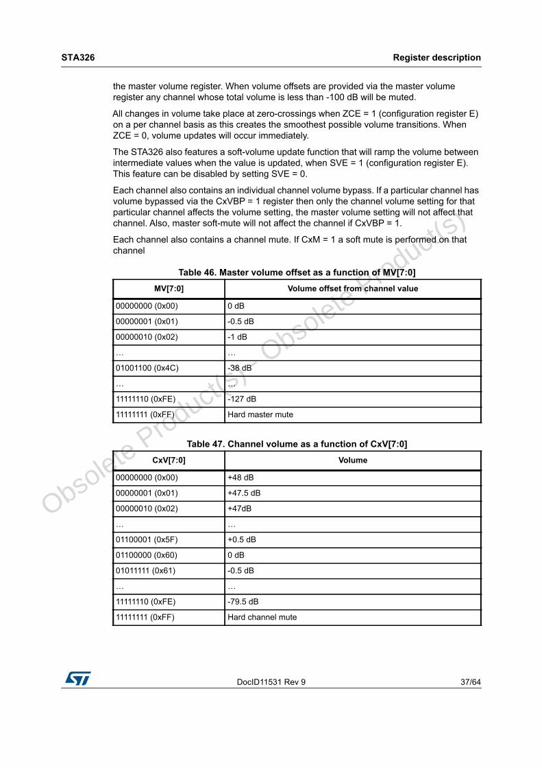
the master volume register. When volume offsets are provided via the master volume register any channel whose total volume is less than -100 dB will be muted.
All changes in volume take place at zero-crossings when ZCE = 1 (configuration register E) on a per channel basis as this creates the smoothest possible volume transitions. When ZCE = 0, volume updates will occur immediately.
The STA326 also features a soft-volume update function that will ramp the volume between intermediate values when the value is updated, when SVE = 1 (configuration register E). This feature can be disabled by setting SVE = 0.
Each channel also contains an individual channel volume bypass. If a particular channel has volume bypassed via the CxVBP = 1 register then only the channel volume setting for that particular channel affects the volume setting, the master volume setting will not affect that channel. Also, master soft-mute will not affect the channel if CxVBP = 1.
Each channel also contains a channel mute. If CxM = 1 a soft mute is performed on that channel
Table 46. Master volume offset as a function of MV[7:0] MV[7:0] Volume offset from channel value
00000000 (0x00) 0 dB
00000001 (0x01) -0.5 dB
00000010 (0x02) -1 dB
… …
01001100 (0x4C) -38 dB
… …
11111110 (0xFE) -127 dB
11111111 (0xFF) Hard master mute
Table 47. Channel volume as a function of CxV[7:0]CxV[7:0] Volume
00000000 (0x00) +48 dB
00000001 (0x01) +47.5 dB
00000010 (0x02) +47dB
… …
01100001 (0x5F) +0.5 dB
01100000 (0x60) 0 dB
01011111 (0x61) -0.5 dB
… …
11111110 (0xFE) -79.5 dB
11111111 (0xFF) Hard channel mute
O
bsolete Product(
s) - O
bsolete Product(
s)
Register description STA326
38/64 DocID11531 Rev 9
7.8 Automode registers
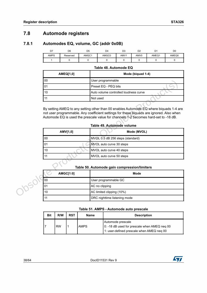
7.8.1 Automodes EQ, volume, GC (addr 0x0B)
By setting AMEQ to any setting other than 00 enables Automode EQ where biquads 1-4 are not user programmable. Any coefficient settings for these biquads are ignored. Also when Automode EQ is used the prescale value for channels 1-2 becomes hard-set to -18 dB.
D7 D6 D5 D4 D3 D2 D1 D0
AMPS Reserved AMGC1 AMGC0 AMV1 AMV0 AMEQ1 AMEQ0
1 0 0 0 0 0 0 0
Table 48. Automode EQAMEQ[1,0] Mode (biquad 1-4)
00 User programmable
01 Preset EQ - PEQ bits
10 Auto volume controlled loudness curve
11 Not used
Table 49. Automode volumeAMV[1,0] Mode (MVOL)
00 MVOL 0.5 dB 256 steps (standard)
01 MVOL auto curve 30 steps
10 MVOL auto curve 40 steps
11 MVOL auto curve 50 steps
Table 50. Automode gain compression/limitersAMGC[1:0] Mode
00 User programmable GC
01 AC no clipping
10 AC limited clipping (10%)
11 DRC nighttime listening mode
Table 51. AMPS - Automode auto prescaleBit R/W RST Name Description
7 RW 1 AMPSAutomode prescale0: -18 dB used for prescale when AMEQ neq 001: user-defined prescale when AMEQ neq 00
O
bsolete Product(
s) - O
bsolete Product(
s)
DocID11531 Rev 9 39/64
STA326 Register description
64
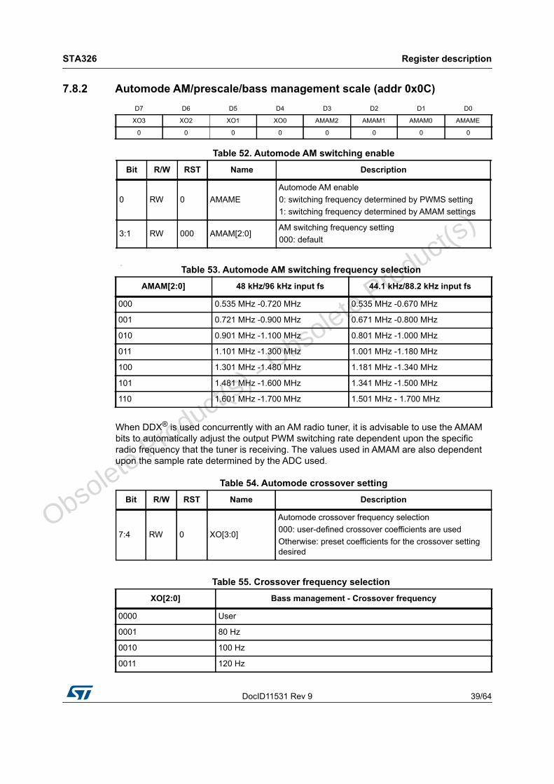
7.8.2 Automode AM/prescale/bass management scale (addr 0x0C)
n
When DDX® is used concurrently with an AM radio tuner, it is advisable to use the AMAM bits to automatically adjust the output PWM switching rate dependent upon the specific radio frequency that the tuner is receiving. The values used in AMAM are also dependent upon the sample rate determined by the ADC used.
D7 D6 D5 D4 D3 D2 D1 D0
XO3 XO2 XO1 XO0 AMAM2 AMAM1 AMAM0 AMAME
0 0 0 0 0 0 0 0
Table 52. Automode AM switching enableBit R/W RST Name Description
0 RW 0 AMAMEAutomode AM enable0: switching frequency determined by PWMS setting1: switching frequency determined by AMAM settings
3:1 RW 000 AMAM[2:0]AM switching frequency setting000: default
Table 53. Automode AM switching frequency selection AMAM[2:0] 48 kHz/96 kHz input fs 44.1 kHz/88.2 kHz input fs
000 0.535 MHz -0.720 MHz 0.535 MHz -0.670 MHz
001 0.721 MHz -0.900 MHz 0.671 MHz -0.800 MHz
010 0.901 MHz -1.100 MHz 0.801 MHz -1.000 MHz
011 1.101 MHz -1.300 MHz 1.001 MHz -1.180 MHz
100 1.301 MHz -1.480 MHz 1.181 MHz -1.340 MHz
101 1.481 MHz -1.600 MHz 1.341 MHz -1.500 MHz
110 1.601 MHz -1.700 MHz 1.501 MHz - 1.700 MHz
Table 54. Automode crossover settingBit R/W RST Name Description
7:4 RW 0 XO[3:0]
Automode crossover frequency selection000: user-defined crossover coefficients are usedOtherwise: preset coefficients for the crossover setting desired
Table 55. Crossover frequency selection XO[2:0] Bass management - Crossover frequency
0000 User
0001 80 Hz
0010 100 Hz
0011 120 Hz
O
bsolete Product(
s) - O
bsolete Product(
s)
Register description STA326
40/64 DocID11531 Rev 9
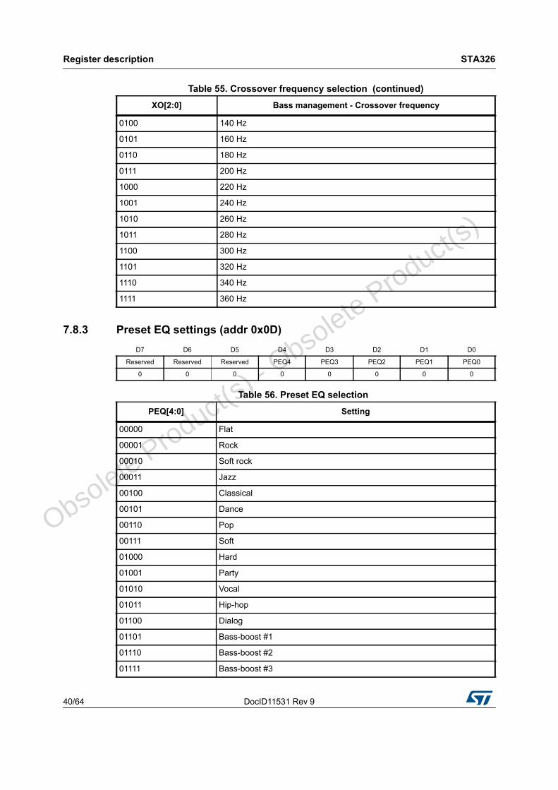
7.8.3 Preset EQ settings (addr 0x0D)
0100 140 Hz
0101 160 Hz
0110 180 Hz
0111 200 Hz
1000 220 Hz
1001 240 Hz
1010 260 Hz
1011 280 Hz
1100 300 Hz
1101 320 Hz
1110 340 Hz
1111 360 Hz
Table 55. Crossover frequency selection (continued)XO[2:0] Bass management - Crossover frequency
D7 D6 D5 D4 D3 D2 D1 D0
Reserved Reserved Reserved PEQ4 PEQ3 PEQ2 PEQ1 PEQ0
0 0 0 0 0 0 0 0
Table 56. Preset EQ selection PEQ[4:0] Setting
00000 Flat
00001 Rock
00010 Soft rock
00011 Jazz
00100 Classical
00101 Dance
00110 Pop
00111 Soft
01000 Hard
01001 Party
01010 Vocal
01011 Hip-hop
01100 Dialog
01101 Bass-boost #1
01110 Bass-boost #2
01111 Bass-boost #3
O
bsolete Product(
s) - O
bsolete Product(
s)
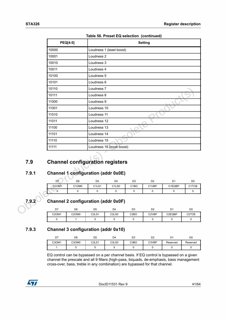
DocID11531 Rev 9 41/64
STA326 Register description
64
7.9 Channel configuration registers
7.9.1 Channel 1 configuration (addr 0x0E)
7.9.2 Channel 2 configuration (addr 0x0F)
7.9.3 Channel 3 configuration (addr 0x10)
EQ control can be bypassed on a per channel basis. If EQ control is bypassed on a given channel the prescale and all 9 filters (high-pass, biquads, de-emphasis, bass management cross-over, bass, treble in any combination) are bypassed for that channel.
10000 Loudness 1 (least boost)
10001 Loudness 2
10010 Loudness 3
10011 Loudness 4
10100 Loudness 5
10101 Loudness 6
10110 Loudness 7
10111 Loudness 8
11000 Loudness 9
11001 Loudness 10
11010 Loudness 11
11011 Loudness 12
11100 Loudness 13
11101 Loudness 14
11110 Loudness 15
11111 Loudness 16 (most boost)
Table 56. Preset EQ selection (continued)PEQ[4:0] Setting
D7 D6 D5 D4 D3 D2 D1 D0
C1OM1 C1OM0 C1LS1 C1LS0 C1BO C1VBP C1EQBP C1TCB
0 0 0 0 0 0 0 0
D7 D6 D5 D4 D3 D2 D1 D0
C2OM1 C2OM0 C2LS1 C2LS0 C2BO C2VBP C2EQBP C2TCB
0 1 0 0 0 0 0 0
D7 D6 D5 D4 D3 D2 D1 D0
C3OM1 C3OM0 C3LS1 C3LS0 C3BO C3VBP Reserved Reserved
1 0 0 0 0 0 0 0
O
bsolete Product(
s) - O
bsolete Product(
s)
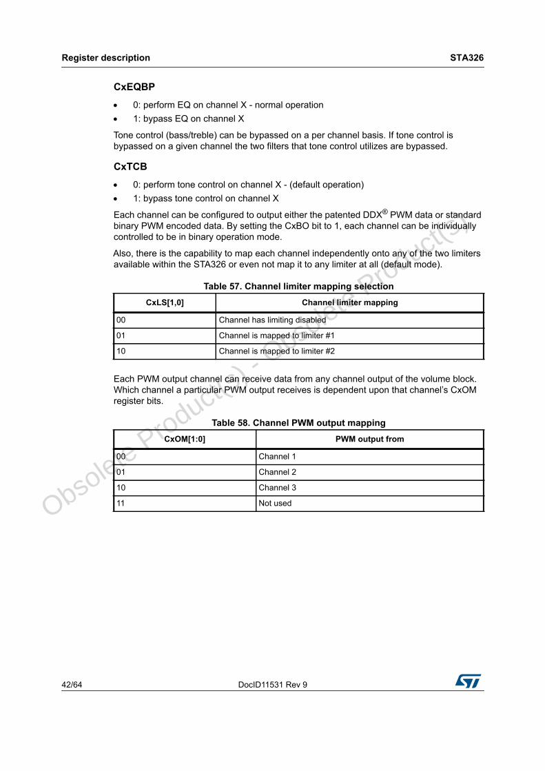
Register description STA326
42/64 DocID11531 Rev 9
CxEQBP
0: perform EQ on channel X - normal operation 1: bypass EQ on channel X
Tone control (bass/treble) can be bypassed on a per channel basis. If tone control is bypassed on a given channel the two filters that tone control utilizes are bypassed.
CxTCB
0: perform tone control on channel X - (default operation) 1: bypass tone control on channel X
Each channel can be configured to output either the patented DDX® PWM data or standard binary PWM encoded data. By setting the CxBO bit to 1, each channel can be individually controlled to be in binary operation mode.
Also, there is the capability to map each channel independently onto any of the two limiters available within the STA326 or even not map it to any limiter at all (default mode).
Each PWM output channel can receive data from any channel output of the volume block. Which channel a particular PWM output receives is dependent upon that channel’s CxOM register bits.
Table 57. Channel limiter mapping selectionCxLS[1,0] Channel limiter mapping
00 Channel has limiting disabled
01 Channel is mapped to limiter #1
10 Channel is mapped to limiter #2
Table 58. Channel PWM output mappingCxOM[1:0] PWM output from
00 Channel 1
01 Channel 2
10 Channel 3
11 Not used
O
bsolete Product(
s) - O
bsolete Product(
s)
DocID11531 Rev 9 43/64
STA326 Register description
64
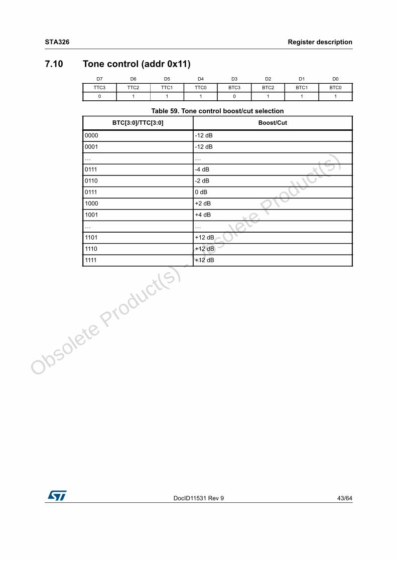
7.10 Tone control (addr 0x11)
D7 D6 D5 D4 D3 D2 D1 D0
TTC3 TTC2 TTC1 TTC0 BTC3 BTC2 BTC1 BTC0
0 1 1 1 0 1 1 1
Table 59. Tone control boost/cut selectionBTC[3:0]/TTC[3:0] Boost/Cut
0000 -12 dB
0001 -12 dB
… …
0111 -4 dB
0110 -2 dB
0111 0 dB
1000 +2 dB
1001 +4 dB
… …
1101 +12 dB
1110 +12 dB
1111 +12 dB
O
bsolete Product(
s) - O
bsolete Product(
s)
Register description STA326
44/64 DocID11531 Rev 9
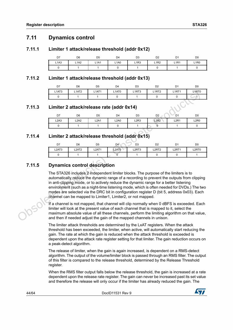
7.11 Dynamics control
7.11.1 Limiter 1 attack/release threshold (addr 0x12)
7.11.2 Limiter 1 attack/release threshold (addr 0x13)
7.11.3 Limiter 2 attack/release rate (addr 0x14)
7.11.4 Limiter 2 attack/release threshold (addr 0x15)
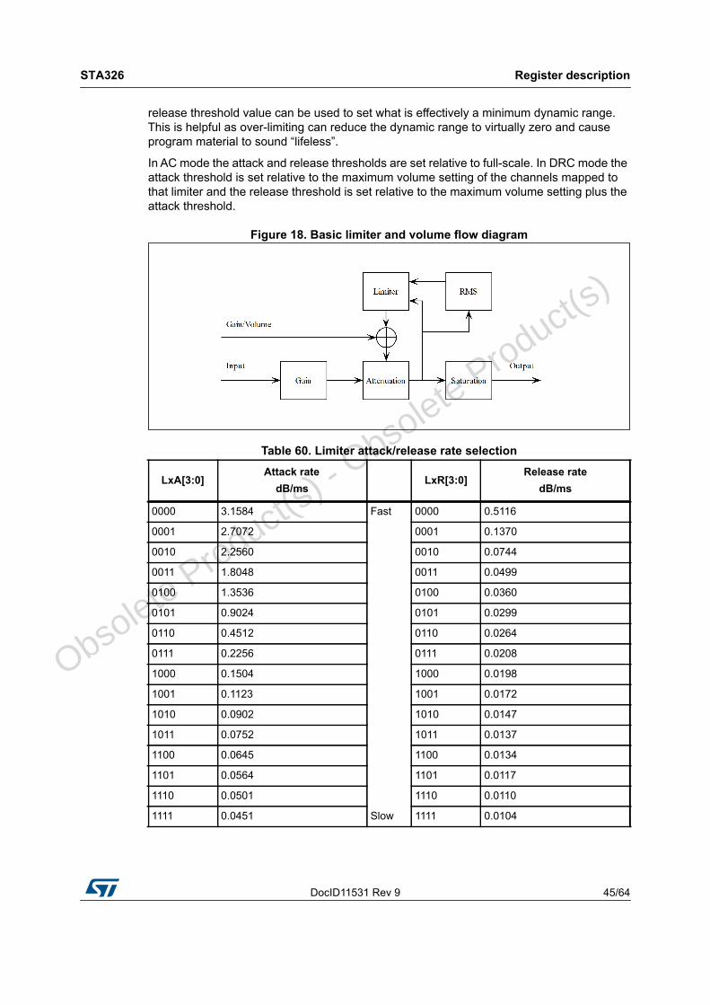
7.11.5 Dynamics control descriptionThe STA326 includes 2 independent limiter blocks. The purpose of the limiters is to automatically reduce the dynamic range of a recording to prevent the outputs from clipping in anti-clipping mode, or to actively reduce the dynamic range for a better listening environment (such as a night-time listening mode, which is often needed for DVDs.) The two modes are selected via the DRC bit in configuration register D (bit 5, address 0x03). Each channel can be mapped to Limiter1, Limiter2, or not mapped.
If a channel is not mapped, that channel will clip normally when 0 dBFS is exceeded. Each limiter will look at the present value of each channel that is mapped to it, select the maximum absolute value of all these channels, perform the limiting algorithm on that value, and then if needed adjust the gain of the mapped channels in unison.
The limiter attack thresholds are determined by the LxAT registers. When the attack threshold has been exceeded, the limiter, when active, will automatically start reducing the gain. The rate at which the gain is reduced when the attack threshold is exceeded is dependent upon the attack rate register setting for that limiter. The gain reduction occurs on a peak-detect algorithm.
The release of limiter, when the gain is again increased, is dependent on a RMS-detect algorithm. The output of the volume/limiter block is passed through an RMS filter. The output of this filter is compared to the release threshold, determined by the Release Threshold register.
When the RMS filter output falls below the release threshold, the gain is increased at a rate dependent upon the release rate register. The gain can never be increased past its set value and therefore the release will only occur if the limiter has already reduced the gain. The
D7 D6 D5 D4 D3 D2 D1 D0
L1A3 L1A2 L1A1 L1A0 L1R3 L1R2 L1R1 L1R0
0 1 1 0 1 0 1 0
D7 D6 D5 D4 D3 D2 D1 D0
L1AT3 L1AT2 L1AT1 L1AT0 L1RT3 L1RT2 L1RT1 L1RT0
0 1 1 0 1 0 0 1
D7 D6 D5 D4 D3 D2 D1 D0
L2A3 L2A2 L2A1 L2A0 L2R3 L2R2 L2R1 L2R0
0 1 1 0 1 0 1 0
D7 D6 D5 D4 D3 D2 D1 D0
L2AT3 L2AT2 L2AT1 L2AT0 L2RT3 L2RT2 L2RT1 L2RT0
0 1 1 0 1 0 0 1
O
bsolete Product(
s) - O
bsolete Product(
s)
DocID11531 Rev 9 45/64
STA326 Register description
64
release threshold value can be used to set what is effectively a minimum dynamic range. This is helpful as over-limiting can reduce the dynamic range to virtually zero and cause program material to sound “lifeless”.
In AC mode the attack and release thresholds are set relative to full-scale. In DRC mode the attack threshold is set relative to the maximum volume setting of the channels mapped to that limiter and the release threshold is set relative to the maximum volume setting plus the attack threshold.
Figure 18. Basic limiter and volume flow diagram
Table 60. Limiter attack/release rate selection
LxA[3:0]Attack rate
dB/msLxR[3:0]
Release rate dB/ms
0000 3.1584 Fast 0000 0.5116
0001 2.7072 0001 0.1370
0010 2.2560 0010 0.0744
0011 1.8048 0011 0.0499
0100 1.3536 0100 0.0360
0101 0.9024 0101 0.0299
0110 0.4512 0110 0.0264
0111 0.2256 0111 0.0208
1000 0.1504 1000 0.0198
1001 0.1123 1001 0.0172
1010 0.0902 1010 0.0147
1011 0.0752 1011 0.0137
1100 0.0645 1100 0.0134
1101 0.0564 1101 0.0117
1110 0.0501 1110 0.0110
1111 0.0451 Slow 1111 0.0104
O
bsolete Product(
s) - O
bsolete Product(
s)
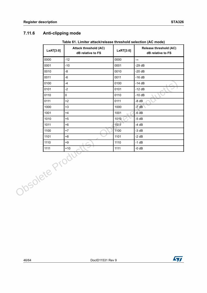
Register description STA326
46/64 DocID11531 Rev 9
7.11.6 Anti-clipping mode
Table 61. Limiter attack/release threshold selection (AC mode)
LxAT[3:0]Attack threshold (AC)
dB relative to FSLxRT[3:0]
Release threshold (AC)dB relative to FS
0000 -12 0000 -
0001 -10 0001 -29 dB
0010 -8 0010 -20 dB
0011 -6 0011 -16 dB
0100 -4 0100 -14 dB
0101 -2 0101 -12 dB
0110 0 0110 -10 dB
0111 +2 0111 -8 dB
1000 +3 1000 -7 dB
1001 +4 1001 -6 dB
1010 +5 1010 -5 dB
1011 +6 1011 -4 dB
1100 +7 1100 -3 dB
1101 +8 1101 -2 dB
1110 +9 1110 -1 dB
1111 +10 1111 -0 dB
O
bsolete Product(
s) - O
bsolete Product(
s)
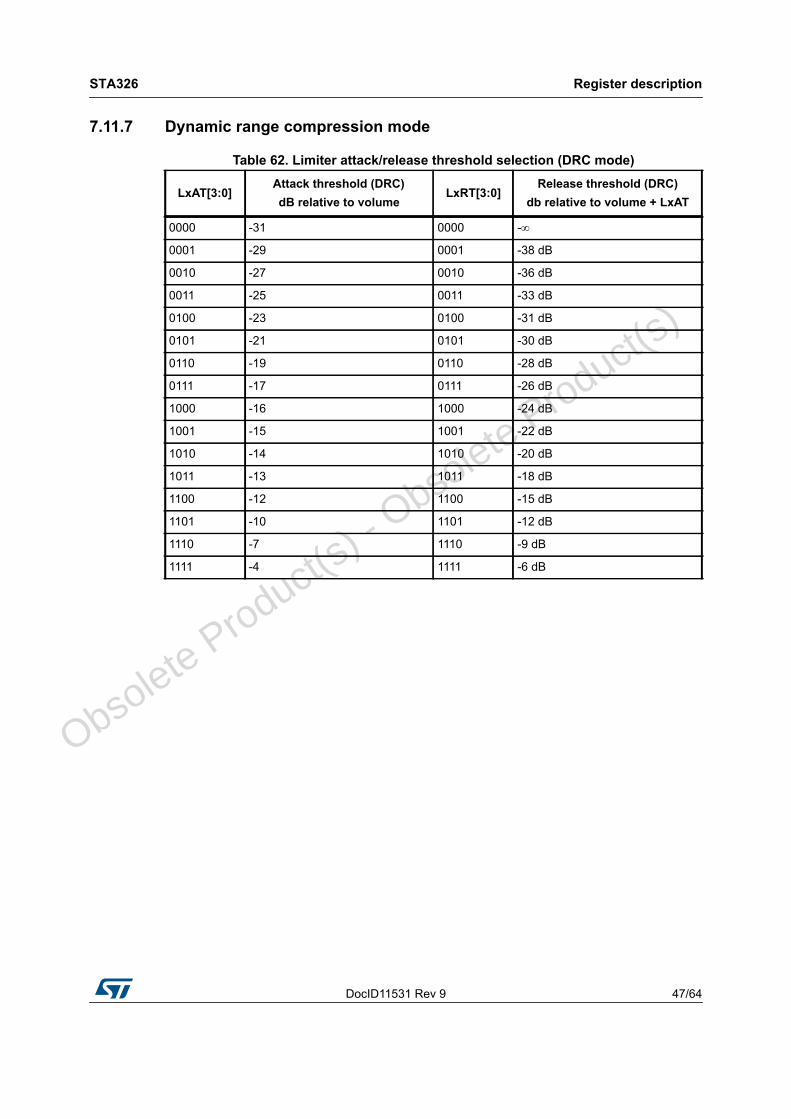
DocID11531 Rev 9 47/64
STA326 Register description
64
7.11.7 Dynamic range compression mode
Table 62. Limiter attack/release threshold selection (DRC mode)
LxAT[3:0]Attack threshold (DRC)dB relative to volume
LxRT[3:0]Release threshold (DRC)
db relative to volume + LxAT
0000 -31 0000 -
0001 -29 0001 -38 dB
0010 -27 0010 -36 dB
0011 -25 0011 -33 dB
0100 -23 0100 -31 dB
0101 -21 0101 -30 dB
0110 -19 0110 -28 dB
0111 -17 0111 -26 dB
1000 -16 1000 -24 dB
1001 -15 1001 -22 dB
1010 -14 1010 -20 dB
1011 -13 1011 -18 dB
1100 -12 1100 -15 dB
1101 -10 1101 -12 dB
1110 -7 1110 -9 dB
1111 -4 1111 -6 dB
O
bsolete Product(
s) - O
bsolete Product(
s)
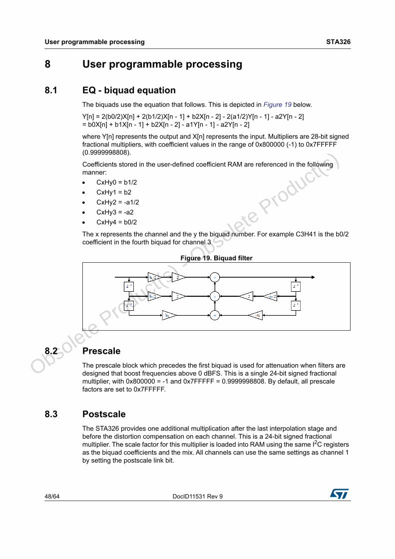
User programmable processing STA326
48/64 DocID11531 Rev 9
8 User programmable processing
8.1 EQ - biquad equationThe biquads use the equation that follows. This is depicted in Figure 19 below.
Y[n] = 2(b0/2)X[n] + 2(b1/2)X[n - 1] + b2X[n - 2] - 2(a1/2)Y[n - 1] - a2Y[n - 2]= b0X[n] + b1X[n - 1] + b2X[n - 2] - a1Y[n - 1] - a2Y[n - 2]
where Y[n] represents the output and X[n] represents the input. Multipliers are 28-bit signed fractional multipliers, with coefficient values in the range of 0x800000 (-1) to 0x7FFFFF (0.9999998808).
Coefficients stored in the user-defined coefficient RAM are referenced in the following manner: CxHy0 = b1/2 CxHy1 = b2 CxHy2 = -a1/2 CxHy3 = -a2 CxHy4 = b0/2
The x represents the channel and the y the biquad number. For example C3H41 is the b0/2 coefficient in the fourth biquad for channel 3
Figure 19. Biquad filter
8.2 PrescaleThe prescale block which precedes the first biquad is used for attenuation when filters are designed that boost frequencies above 0 dBFS. This is a single 24-bit signed fractional multiplier, with 0x800000 = -1 and 0x7FFFFF = 0.9999998808. By default, all prescale factors are set to 0x7FFFFF.
8.3 PostscaleThe STA326 provides one additional multiplication after the last interpolation stage and before the distortion compensation on each channel. This is a 24-bit signed fractional multiplier. The scale factor for this multiplier is loaded into RAM using the same I2C registers as the biquad coefficients and the mix. All channels can use the same settings as channel 1 by setting the postscale link bit.
O
bsolete Product(
s) - O
bsolete Product(
s)
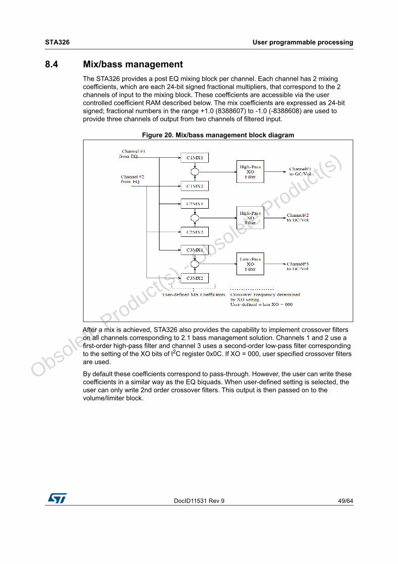
DocID11531 Rev 9 49/64
STA326 User programmable processing
64
8.4 Mix/bass managementThe STA326 provides a post EQ mixing block per channel. Each channel has 2 mixing coefficients, which are each 24-bit signed fractional multipliers, that correspond to the 2 channels of input to the mixing block. These coefficients are accessible via the user controlled coefficient RAM described below. The mix coefficients are expressed as 24-bit signed; fractional numbers in the range +1.0 (8388607) to -1.0 (-8388608) are used to provide three channels of output from two channels of filtered input.
Figure 20. Mix/bass management block diagram
After a mix is achieved, STA326 also provides the capability to implement crossover filters on all channels corresponding to 2.1 bass management solution. Channels 1 and 2 use a first-order high-pass filter and channel 3 uses a second-order low-pass filter corresponding to the setting of the XO bits of I2C register 0x0C. If XO = 000, user specified crossover filters are used.
By default these coefficients correspond to pass-through. However, the user can write these coefficients in a similar way as the EQ biquads. When user-defined setting is selected, the user can only write 2nd order crossover filters. This output is then passed on to the volume/limiter block.
Obso
lete Product(s)
- Obso
lete Product(s)
User programmable processing STA326
50/64 DocID11531 Rev 9
8.5 Calculating 24-bit signed fractional numbers from a dB valueThe prescale, mixing, and postscale functions of the STA326 use 24-bit signed fractional multipliers to attenuate signals. These attenuations can also invert the phase and therefore range in value from -1 to +1. It is possible to calculate the coefficient to utilize for a given negative dB value (attenuation) via the equations below. Non-inverting phase numbers 0 to +1: Coefficient = round(8388607 * 10(dB / 20)) Inverting phase numbers 0 to -1: Coefficient = 16777216 - round(8388607 * 10(dB / 20))
As can be seen by the preceding equations, the value for positive phase 0 dB is 0x7FFFFF and the value for negative phase 0 dB is 0x800000.
8.6 User-defined coefficient RAM
8.6.1 Coefficient address register 1 (addr 0x16)
8.6.2 Coefficient b1data register bits 23:16 (addr 0x17)
8.6.3 Coefficient b1data register bits 15:8 (addr 0x18)
8.6.4 Coefficient b1data register bits 7:0 (addr 0x19)
8.6.5 Coefficient b2 data register bits 23:16 (addr 0x1A)
D7 D6 D5 D4 D3 D2 D1 D0
CFA7 CFA6 CFA5 CFA4 CFA3 CFA2 CFA1 CFA0
0 0 0 0 0 0 0 0
D7 D6 D5 D4 D3 D2 D1 D0
C1B23 C1B22 C1B21 C1B20 C1B19 C1B18 C1B17 C1B16
0 0 0 0 0 0 0 0
D7 D6 D5 D4 D3 D2 D1 D0
C1B15 C1B14 C1B13 C1B12 C1B11 C1B10 C1B9 C1B8
0 0 0 0 0 0 0 0
D7 D6 D5 D4 D3 D2 D1 D0
C1B7 C1B6 C1B5 C1B4 C1B3 C1B2 C1B1 C1B0
0 0 0 0 0 0 0 0
D7 D6 D5 D4 D3 D2 D1 D0
C2B23 C2B22 C2B21 C2B20 C2B19 C2B18 C2B17 C2B16
0 0 0 0 0 0 0 0
O
bsolete Product(
s) - O
bsolete Product(
s)
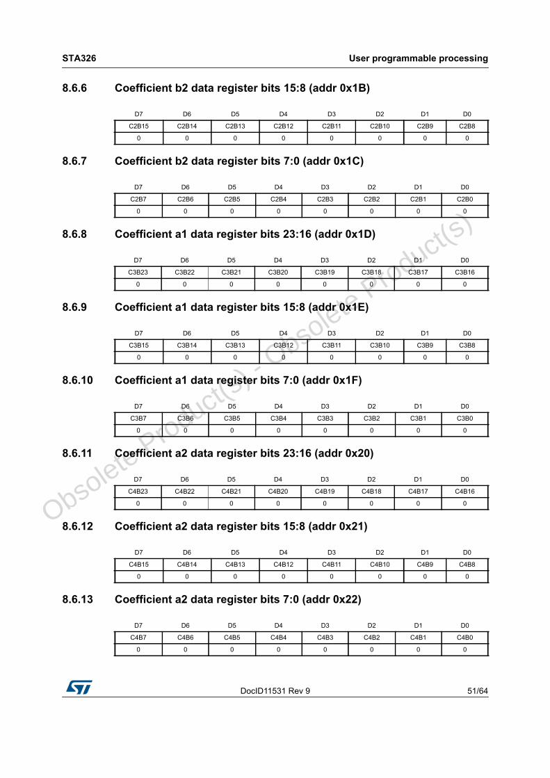
DocID11531 Rev 9 51/64
STA326 User programmable processing
64
8.6.6 Coefficient b2 data register bits 15:8 (addr 0x1B)
8.6.7 Coefficient b2 data register bits 7:0 (addr 0x1C)
8.6.8 Coefficient a1 data register bits 23:16 (addr 0x1D)
8.6.9 Coefficient a1 data register bits 15:8 (addr 0x1E)
8.6.10 Coefficient a1 data register bits 7:0 (addr 0x1F)
8.6.11 Coefficient a2 data register bits 23:16 (addr 0x20)
8.6.12 Coefficient a2 data register bits 15:8 (addr 0x21)
8.6.13 Coefficient a2 data register bits 7:0 (addr 0x22)
D7 D6 D5 D4 D3 D2 D1 D0
C2B15 C2B14 C2B13 C2B12 C2B11 C2B10 C2B9 C2B8
0 0 0 0 0 0 0 0
D7 D6 D5 D4 D3 D2 D1 D0
C2B7 C2B6 C2B5 C2B4 C2B3 C2B2 C2B1 C2B0
0 0 0 0 0 0 0 0
D7 D6 D5 D4 D3 D2 D1 D0
C3B23 C3B22 C3B21 C3B20 C3B19 C3B18 C3B17 C3B16
0 0 0 0 0 0 0 0
D7 D6 D5 D4 D3 D2 D1 D0
C3B15 C3B14 C3B13 C3B12 C3B11 C3B10 C3B9 C3B8
0 0 0 0 0 0 0 0
D7 D6 D5 D4 D3 D2 D1 D0
C3B7 C3B6 C3B5 C3B4 C3B3 C3B2 C3B1 C3B0
0 0 0 0 0 0 0 0
D7 D6 D5 D4 D3 D2 D1 D0
C4B23 C4B22 C4B21 C4B20 C4B19 C4B18 C4B17 C4B16
0 0 0 0 0 0 0 0
D7 D6 D5 D4 D3 D2 D1 D0
C4B15 C4B14 C4B13 C4B12 C4B11 C4B10 C4B9 C4B8
0 0 0 0 0 0 0 0
D7 D6 D5 D4 D3 D2 D1 D0
C4B7 C4B6 C4B5 C4B4 C4B3 C4B2 C4B1 C4B0
0 0 0 0 0 0 0 0
O
bsolete Product(
s) - O
bsolete Product(
s)
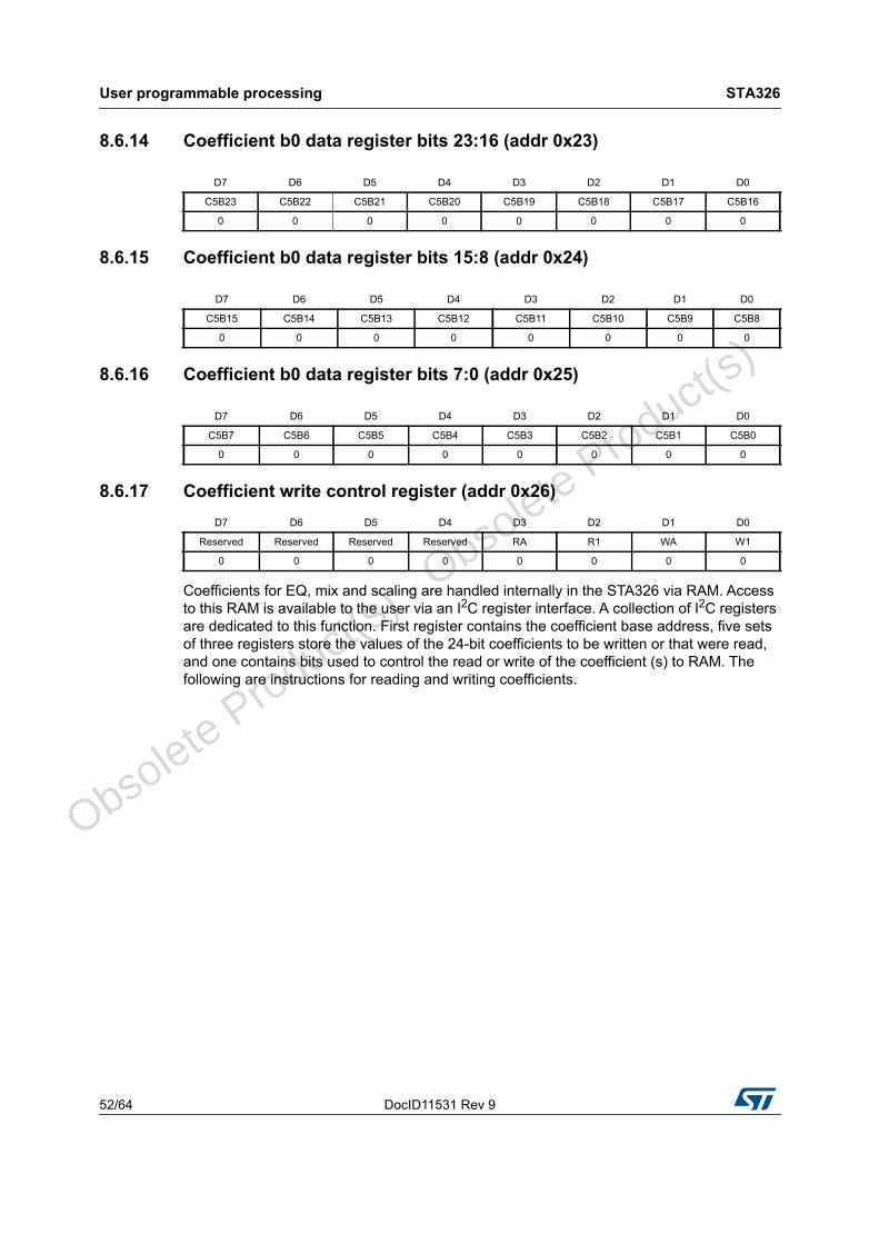
User programmable processing STA326
52/64 DocID11531 Rev 9
8.6.14 Coefficient b0 data register bits 23:16 (addr 0x23)
8.6.15 Coefficient b0 data register bits 15:8 (addr 0x24)
8.6.16 Coefficient b0 data register bits 7:0 (addr 0x25)
8.6.17 Coefficient write control register (addr 0x26)
Coefficients for EQ, mix and scaling are handled internally in the STA326 via RAM. Access to this RAM is available to the user via an I2C register interface. A collection of I2C registers are dedicated to this function. First register contains the coefficient base address, five sets of three registers store the values of the 24-bit coefficients to be written or that were read, and one contains bits used to control the read or write of the coefficient (s) to RAM. The following are instructions for reading and writing coefficients.
D7 D6 D5 D4 D3 D2 D1 D0
C5B23 C5B22 C5B21 C5B20 C5B19 C5B18 C5B17 C5B16
0 0 0 0 0 0 0 0
D7 D6 D5 D4 D3 D2 D1 D0
C5B15 C5B14 C5B13 C5B12 C5B11 C5B10 C5B9 C5B8
0 0 0 0 0 0 0 0
D7 D6 D5 D4 D3 D2 D1 D0
C5B7 C5B6 C5B5 C5B4 C5B3 C5B2 C5B1 C5B0
0 0 0 0 0 0 0 0
D7 D6 D5 D4 D3 D2 D1 D0
Reserved Reserved Reserved Reserved RA R1 WA W1
0 0 0 0 0 0 0 0
O
bsolete Product(
s) - O
bsolete Product(
s)
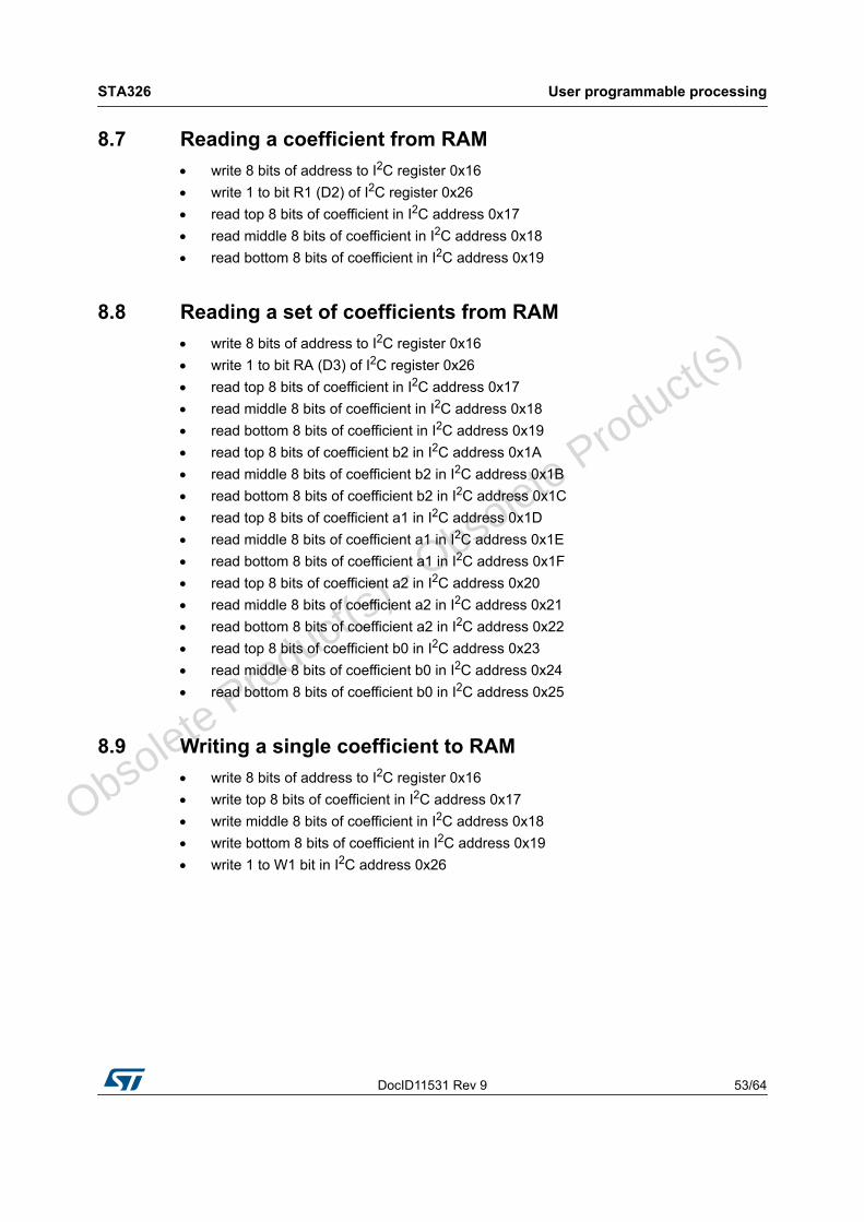
DocID11531 Rev 9 53/64
STA326 User programmable processing
64
8.7 Reading a coefficient from RAM write 8 bits of address to I2C register 0x16 write 1 to bit R1 (D2) of I2C register 0x26 read top 8 bits of coefficient in I2C address 0x17 read middle 8 bits of coefficient in I2C address 0x18 read bottom 8 bits of coefficient in I2C address 0x19
8.8 Reading a set of coefficients from RAM write 8 bits of address to I2C register 0x16 write 1 to bit RA (D3) of I2C register 0x26 read top 8 bits of coefficient in I2C address 0x17 read middle 8 bits of coefficient in I2C address 0x18 read bottom 8 bits of coefficient in I2C address 0x19 read top 8 bits of coefficient b2 in I2C address 0x1A read middle 8 bits of coefficient b2 in I2C address 0x1B read bottom 8 bits of coefficient b2 in I2C address 0x1C read top 8 bits of coefficient a1 in I2C address 0x1D read middle 8 bits of coefficient a1 in I2C address 0x1E read bottom 8 bits of coefficient a1 in I2C address 0x1F read top 8 bits of coefficient a2 in I2C address 0x20 read middle 8 bits of coefficient a2 in I2C address 0x21 read bottom 8 bits of coefficient a2 in I2C address 0x22 read top 8 bits of coefficient b0 in I2C address 0x23 read middle 8 bits of coefficient b0 in I2C address 0x24 read bottom 8 bits of coefficient b0 in I2C address 0x25
8.9 Writing a single coefficient to RAM write 8 bits of address to I2C register 0x16 write top 8 bits of coefficient in I2C address 0x17 write middle 8 bits of coefficient in I2C address 0x18 write bottom 8 bits of coefficient in I2C address 0x19 write 1 to W1 bit in I2C address 0x26
Obso
lete Product(s)
- Obso
lete Product(s)
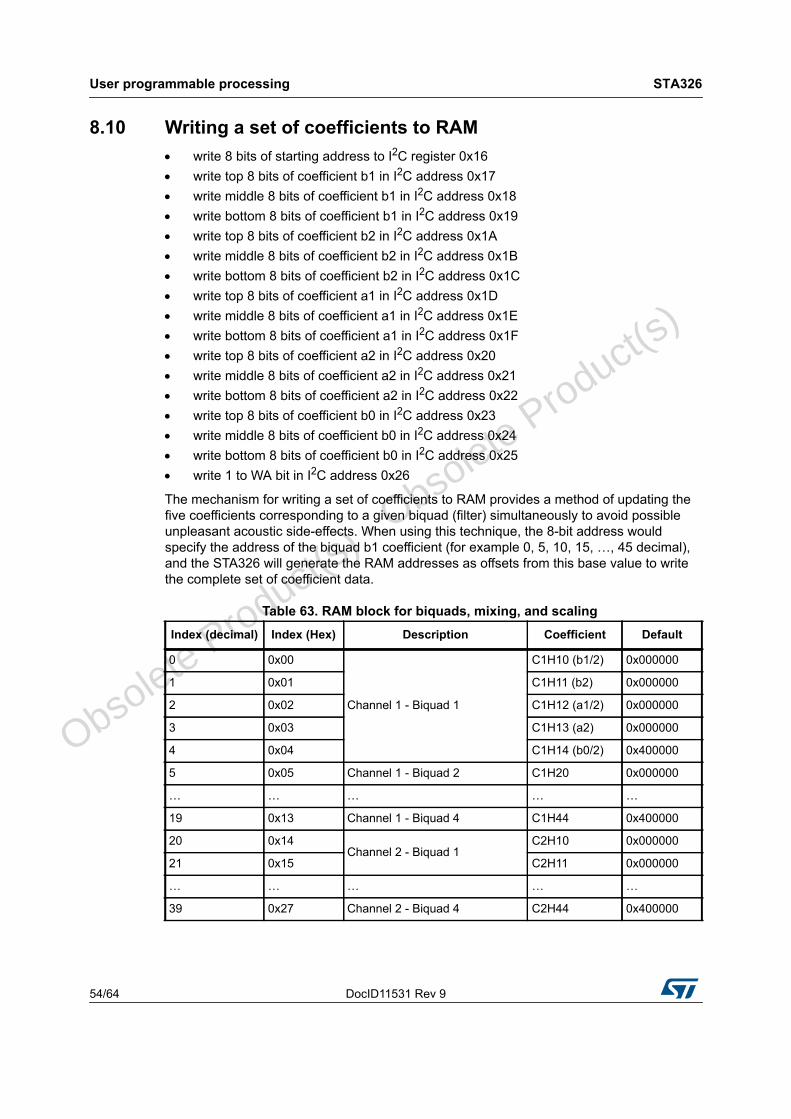
User programmable processing STA326
54/64 DocID11531 Rev 9
8.10 Writing a set of coefficients to RAM write 8 bits of starting address to I2C register 0x16 write top 8 bits of coefficient b1 in I2C address 0x17 write middle 8 bits of coefficient b1 in I2C address 0x18 write bottom 8 bits of coefficient b1 in I2C address 0x19 write top 8 bits of coefficient b2 in I2C address 0x1A write middle 8 bits of coefficient b2 in I2C address 0x1B write bottom 8 bits of coefficient b2 in I2C address 0x1C write top 8 bits of coefficient a1 in I2C address 0x1D write middle 8 bits of coefficient a1 in I2C address 0x1E write bottom 8 bits of coefficient a1 in I2C address 0x1F write top 8 bits of coefficient a2 in I2C address 0x20 write middle 8 bits of coefficient a2 in I2C address 0x21 write bottom 8 bits of coefficient a2 in I2C address 0x22 write top 8 bits of coefficient b0 in I2C address 0x23 write middle 8 bits of coefficient b0 in I2C address 0x24 write bottom 8 bits of coefficient b0 in I2C address 0x25 write 1 to WA bit in I2C address 0x26
The mechanism for writing a set of coefficients to RAM provides a method of updating the five coefficients corresponding to a given biquad (filter) simultaneously to avoid possible unpleasant acoustic side-effects. When using this technique, the 8-bit address would specify the address of the biquad b1 coefficient (for example 0, 5, 10, 15, …, 45 decimal), and the STA326 will generate the RAM addresses as offsets from this base value to write the complete set of coefficient data.
Table 63. RAM block for biquads, mixing, and scaling Index (decimal) Index (Hex) Description Coefficient Default
0 0x00
Channel 1 - Biquad 1
C1H10 (b1/2) 0x000000
1 0x01 C1H11 (b2) 0x000000
2 0x02 C1H12 (a1/2) 0x000000
3 0x03 C1H13 (a2) 0x000000
4 0x04 C1H14 (b0/2) 0x400000
5 0x05 Channel 1 - Biquad 2 C1H20 0x000000
… … … … …
19 0x13 Channel 1 - Biquad 4 C1H44 0x400000
20 0x14Channel 2 - Biquad 1
C2H10 0x000000
21 0x15 C2H11 0x000000
… … … … …
39 0x27 Channel 2 - Biquad 4 C2H44 0x400000
O
bsolete Product(
s) - O
bsolete Product(
s)
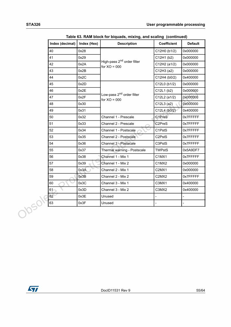
DocID11531 Rev 9 55/64
STA326 User programmable processing
64
40 0x28
High-pass 2nd order filterfor XO = 000
C12H0 (b1/2) 0x000000
41 0x29 C12H1 (b2) 0x000000
42 0x2A C12H2 (a1/2) 0x000000
43 0x2B C12H3 (a2) 0x000000
44 0x2C C12H4 (b0/2) 0x400000
45 0x2D
Low-pass 2nd order filterfor XO = 000
C12L0 (b1/2) 0x000000
46 0x2E C12L1 (b2) 0x000000
47 0x2F C12L2 (a1/2) 0x000000
48 0x30 C12L3 (a2) 0x000000
49 0x31 C12L4 (b0/2) 0x400000
50 0x32 Channel 1 - Prescale C1PreS 0x7FFFFF
51 0x33 Channel 2 - Prescale C2PreS 0x7FFFFF
52 0x34 Channel 1 - Postscale C1PstS 0x7FFFFF
53 0x35 Channel 2 - Postscale C2PstS 0x7FFFFF
54 0x36 Channel 3 - Postscale C3PstS 0x7FFFFF
55 0x37 Thermal warning - Postscale TWPstS 0x5A9DF7
56 0x38 Channel 1 - Mix 1 C1MX1 0x7FFFFF
57 0x39 Channel 1 - Mix 2 C1MX2 0x000000
58 0x3A Channel 2 - Mix 1 C2MX1 0x000000
59 0x3B Channel 2 - Mix 2 C2MX2 0x7FFFFF
60 0x3C Channel 3 - Mix 1 C3MX1 0x400000
61 0x3D Channel 3 - Mix 2 C3MX2 0x400000
62 0x3E Unused - -
63 0x3F Unused - -
Table 63. RAM block for biquads, mixing, and scaling (continued)Index (decimal) Index (Hex) Description Coefficient Default
O
bsolete Product(
s) - O
bsolete Product(
s)
User programmable processing STA326
56/64 DocID11531 Rev 9
8.11 Variable max power correction (addr 0x27, 0x28)
MPCC bits determine the 16 MSBs of the MPC compensation coefficient. This coefficient is used in place of the default coefficient when MPCV = 1.
8.12 Fault detect recovery (addr 0x2B, 0x2C)
FDRC bits specify the 16-bit fault detect recovery time delay. When FAULT is asserted, the output TRISTATE will be immediately asserted low and held low for the time period specified by this constant. A constant value of 0x0001 in this register is approximately 0.083 ms. The default value of 0x000C specifies approximately 1 ms.
8.13 Status (addr 0x2D)
D7 D6 D5 D4 D3 D2 D1 D0
MPCC15 MPCC14 MPCC13 MPCC12 MPCC11 MPCC10 MPCC9 MPCC8
0 0 1 0 1 1 0 1
MPCC7 MPCC6 MPCC5 MPCC4 MPCC3 MPCC2 MPCC1 MPCC0
1 1 0 0 0 0 0 0
D7 D6 D5 D4 D3 D2 D1 D0
FDRC15 FDRC14 FDRC13 FDRC12 FDRC11 FDRC10 FDRC9 FDRC8
0 0 0 0 0 0 0 0
FDRC7 FDRC6 FDRC5 FDRC4 FDRC3 FDRC2 FDRC1 FDRC0
0 0 0 0 1 1 0 0
D7 D6 D5 D4 D3 D2 D1 D0
PLLUL Reserved Reserved Reserved Reserved Reserved FAULT TWARN
0 0 0 0 0 0 0 0
Table 64. TWARND0 Thermal warning
0 Thermal warning condition
1 Normal operation
Table 65. FAULTD1 IC fault
0 IC fault condition
1 Normal operation
Table 66. PLLULD7 PLL unlocked
0 Normal operation
1 PLL unlocked
O
bsolete Product(
s) - O
bsolete Product(
s)
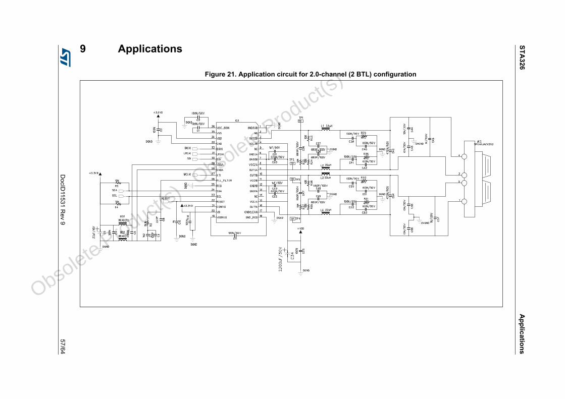
STA326
Applications
DocID
11531 Rev 9
57/64
9 Applications
Figure 21. Application circuit for 2.0-channel (2 BTL) configuration
O
bsolete Product(
s) - O
bsolete Product(
s)
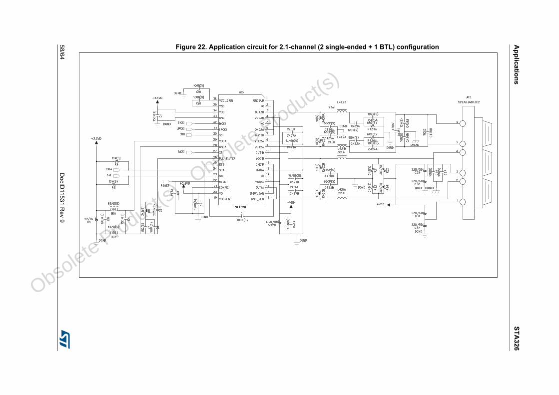
Applications
STA326
58/64D
ocID11531 R
ev 9
Figure 22. Application circuit for 2.1-channel (2 single-ended + 1 BTL) configuration
O
bsolete Product(
s) - O
bsolete Product(
s)
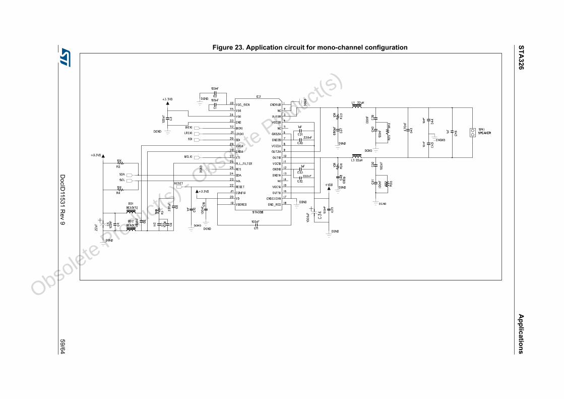
STA326
Applications
DocID
11531 Rev 9
59/64
Figure 23. Application circuit for mono-channel configuration
O
bsolete Product(
s) - O
bsolete Product(
s)
Package mechanical data STA326
60/64 DocID11531 Rev 9
10 Package mechanical data
In order to meet environmental requirements, ST offers these devices in different grades of ECOPACK® packages, depending on their level of environmental compliance. ECOPACK® specifications, grade definitions and product status are available at: www.st.com. ECOPACK® is an ST trademark.
O
bsolete Product(
s) - O
bsolete Product(
s)
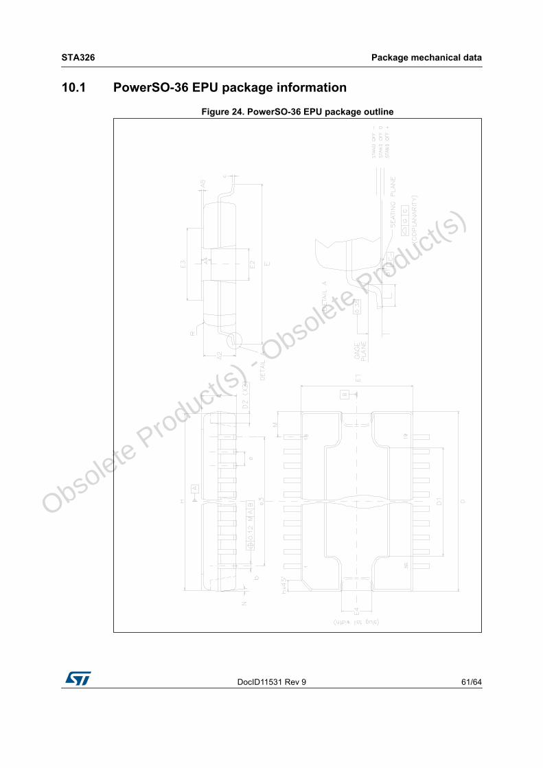
DocID11531 Rev 9 61/64
STA326 Package mechanical data
64
10.1 PowerSO-36 EPU package information
Figure 24. PowerSO-36 EPU package outline
O
bsolete Product(
s) - O
bsolete Product(
s)
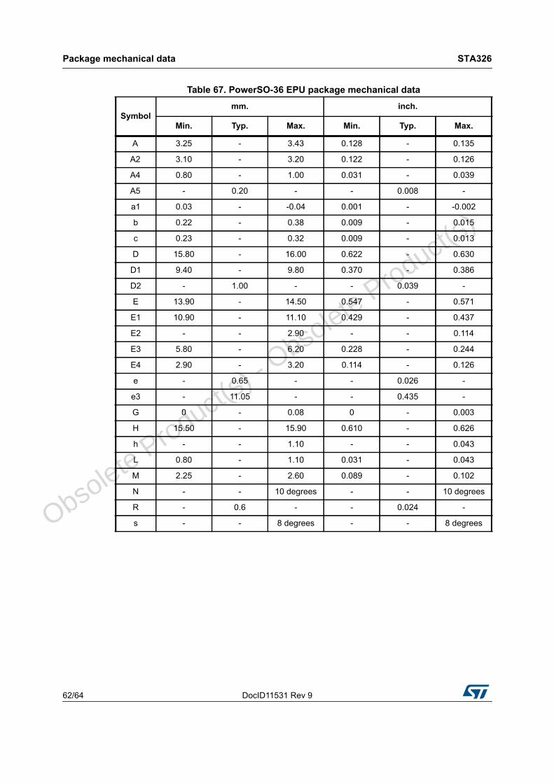
Package mechanical data STA326
62/64 DocID11531 Rev 9
Table 67. PowerSO-36 EPU package mechanical data
Symbolmm. inch.
Min. Typ. Max. Min. Typ. Max.
A 3.25 - 3.43 0.128 - 0.135
A2 3.10 - 3.20 0.122 - 0.126
A4 0.80 - 1.00 0.031 - 0.039
A5 - 0.20 - - 0.008 -
a1 0.03 - -0.04 0.001 - -0.002
b 0.22 - 0.38 0.009 - 0.015
c 0.23 - 0.32 0.009 - 0.013
D 15.80 - 16.00 0.622 - 0.630
D1 9.40 - 9.80 0.370 - 0.386
D2 - 1.00 - - 0.039 -
E 13.90 - 14.50 0.547 - 0.571
E1 10.90 - 11.10 0.429 - 0.437
E2 - - 2.90 - - 0.114
E3 5.80 - 6.20 0.228 - 0.244
E4 2.90 - 3.20 0.114 - 0.126
e - 0.65 - - 0.026 -
e3 - 11.05 - - 0.435 -
G 0 - 0.08 0 - 0.003
H 15.50 - 15.90 0.610 - 0.626
h - - 1.10 - - 0.043
L 0.80 - 1.10 0.031 - 0.043
M 2.25 - 2.60 0.089 - 0.102
N - - 10 degrees - - 10 degrees
R - 0.6 - - 0.024 -
s - - 8 degrees - - 8 degrees
O
bsolete Product(
s) - O
bsolete Product(
s)
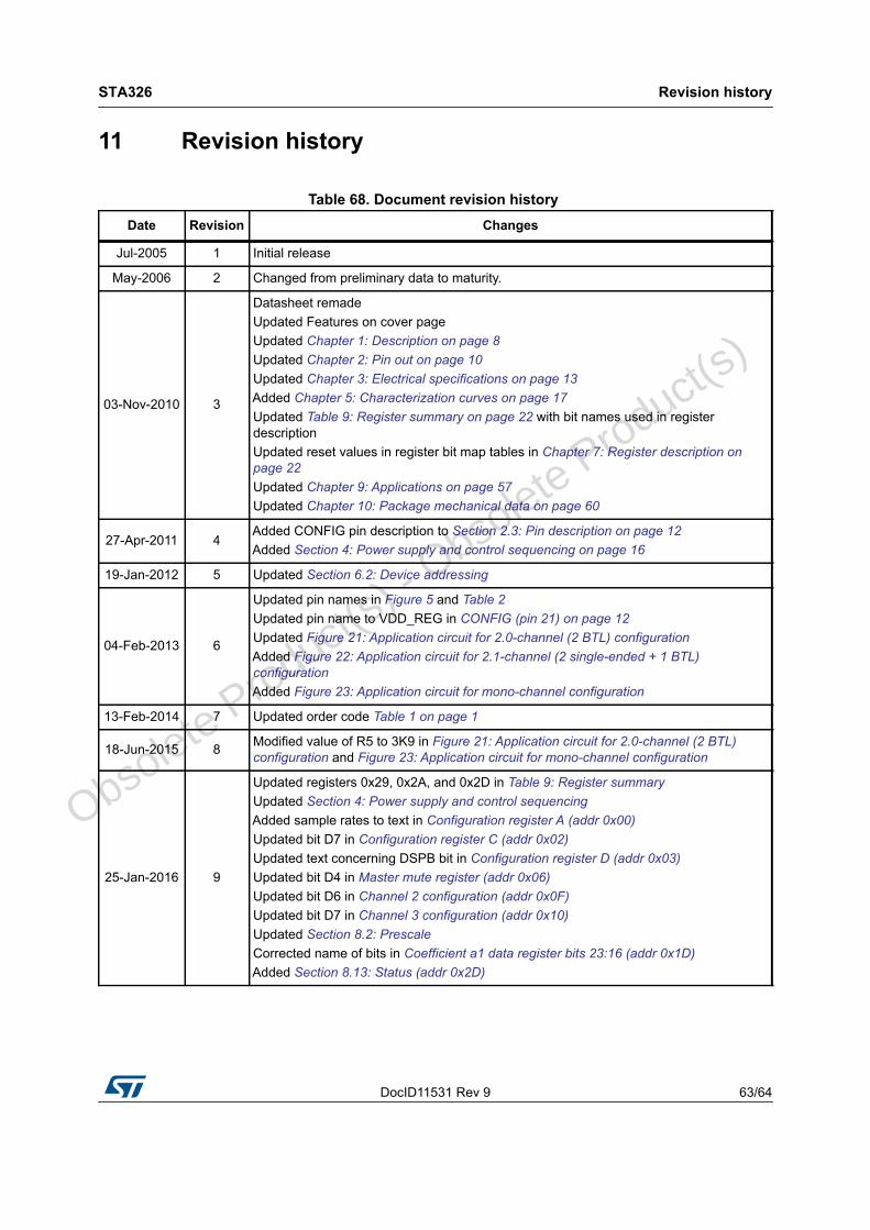
DocID11531 Rev 9 63/64
STA326 Revision history
64
11 Revision history
Table 68. Document revision history Date Revision Changes
Jul-2005 1 Initial release
May-2006 2 Changed from preliminary data to maturity.
03-Nov-2010 3
Datasheet remadeUpdated Features on cover pageUpdated Chapter 1: Description on page 8Updated Chapter 2: Pin out on page 10Updated Chapter 3: Electrical specifications on page 13Added Chapter 5: Characterization curves on page 17Updated Table 9: Register summary on page 22 with bit names used in register descriptionUpdated reset values in register bit map tables in Chapter 7: Register description on page 22 Updated Chapter 9: Applications on page 57Updated Chapter 10: Package mechanical data on page 60
27-Apr-2011 4Added CONFIG pin description to Section 2.3: Pin description on page 12Added Section 4: Power supply and control sequencing on page 16
19-Jan-2012 5 Updated Section 6.2: Device addressing
04-Feb-2013 6
Updated pin names in Figure 5 and Table 2Updated pin name to VDD_REG in CONFIG (pin 21) on page 12Updated Figure 21: Application circuit for 2.0-channel (2 BTL) configurationAdded Figure 22: Application circuit for 2.1-channel (2 single-ended + 1 BTL) configurationAdded Figure 23: Application circuit for mono-channel configuration
13-Feb-2014 7 Updated order code Table 1 on page 1
18-Jun-2015 8 Modified value of R5 to 3K9 in Figure 21: Application circuit for 2.0-channel (2 BTL) configuration and Figure 23: Application circuit for mono-channel configuration
25-Jan-2016 9
Updated registers 0x29, 0x2A, and 0x2D in Table 9: Register summaryUpdated Section 4: Power supply and control sequencingAdded sample rates to text in Configuration register A (addr 0x00)Updated bit D7 in Configuration register C (addr 0x02)Updated text concerning DSPB bit in Configuration register D (addr 0x03)Updated bit D4 in Master mute register (addr 0x06)Updated bit D6 in Channel 2 configuration (addr 0x0F)Updated bit D7 in Channel 3 configuration (addr 0x10)Updated Section 8.2: PrescaleCorrected name of bits in Coefficient a1 data register bits 23:16 (addr 0x1D)Added Section 8.13: Status (addr 0x2D)
O
bsolete Product(
s) - O
bsolete Product(
s)
STA326
64/64 DocID11531 Rev 9
IMPORTANT NOTICE – PLEASE READ CAREFULLY
STMicroelectronics NV and its subsidiaries (“ST”) reserve the right to make changes, corrections, enhancements, modifications, and improvements to ST products and/or to this document at any time without notice. Purchasers should obtain the latest relevant information on ST products before placing orders. ST products are sold pursuant to ST’s terms and conditions of sale in place at the time of order acknowledgement.
Purchasers are solely responsible for the choice, selection, and use of ST products and ST assumes no liability for application assistance or the design of Purchasers’ products.
No license, express or implied, to any intellectual property right is granted by ST herein.
Resale of ST products with provisions different from the information set forth herein shall void any warranty granted by ST for such product.
ST and the ST logo are trademarks of ST. All other product or service names are the property of their respective owners.
Information in this document supersedes and replaces information previously supplied in any prior versions of this document.
© 2016 STMicroelectronics – All rights reserved
O
bsolete Product(
s) - O
bsolete Product(
s)