Embed Size (px)
Citation preview

www.4dsp.com
For Digital Signal Processingdesign & system integration
Onderkant tussenkop op deze lijn
Onderkant kop op deze lijn
www en kader tot hier
rev-1.1
4DSP Analog Design Techniques
4DSP Analog Design TechniquesAnalog-to-digital converters (ADCs) and digital-to-analog
converters (DACs) are essential components of many
electronic systems that require a link between the analog and digital
worlds. 4DSP offers a wide range of FPGA mezzanine card (FMC)
modules that provide high-performance ADC/DAC functionality for
clients in the aerospace, defense, medical and telecom industries
among others. Our top priority is maintaining very high signal integrity
by using appropriate ADC/DAC components from providers such as
Texas Instruments and Analog Devices that deliver the right balance
of conversion resolution and sampling rate. The constraints of the
ruggedized applications that many 4DSP FMC products are desig-
ned for require that low power consumption and resistance to high
temperatures also be factored into our designs.
4DSP is different from some other vendors in the embedded industry
in that we typically get our designs right the first time rather than
planning to release subsequent board versions with refinements
that could have been made to the original design. In this way, we
avoid negative feedback from the marketplace to point out the
shortcomings of a board and inform an inevitable design revision.
Needless to say, our design workflow has been fine-tuned to support
this approach and to comply with AS9100C requirements for quality
management.
Planning and Development4DSP creates a new ADC/DAC board by following a design
control process that starts with a team meeting to determine the
phases of the project and to verify the design control checklist.
The requirements list is also established and reviewed, and risks
are identified, analyzed and mitigated. A design specification that
addresses the product requirements is developed internally with
input potentially from the customer. It may also be necessary to
address regulatory agency requirements. A schematic design is
then created by the design engineer who passes that on to the
layout engineer who designs the PCB. Each engineer generates
all appropriate documentation and design files for their stage of the
process while making sure that all work is reviewed.
The process is overseen by a project manager who is responsible for
guiding the flow of the project through all phases to meet progress
milestones. The project manager approves designs, allocates the
necessary resources, tracks risk management and verifies that all
necessary documentation and records are properly maintained.
Once the design is fine-tuned and approved, it is released for
PCB manufacturing, assembly and validation against requirements.
Finally, any necessary changes are made before the final design is
completed and put into production.
Risk Management and ReviewRisks are identified and their probability and potential impact are
determined during the contract review phase or during the design
and development process. Factors that may complicate the
design effort, such as custom part or component requirements,
are considered and rated. Risk mitigation is ongoing throughout
a project and any necessary supply chain or resource allocation
adjustments are made to avoid project delays or unnecessary
expense. Regular engineering meetings are held during development
to discuss progress and technical issues. During this period, the
project manager monitors design phase approvals, project status,
and risk management changes.
The review process relies on the design control checklist that
individual reviewers follow when verifying documentation and
design files to ensure a thorough assessment of how well a design
is being implemented against the requirements. This helps to avoid
a situation where any one reviewer may tend to focus on a particular
area of interest or specialty while scrutinizing other areas less closely.
This method contrasts with a group review process where a
meeting of several engineers is held to review the design during
development. The latter is problematic because there can be a lack
of clarity about who is responsible for following up on all necessary
issues or changes.
Design ChallengesThe most important technical consideration when designing an
ADC/DAC board is maintaining the integrity of the analog signal.
This is accomplished by generating a high-quality clock signal
using the best PLL and oscillators for the application, and ensuring
that the analog front end, or the circuitry between connector
and ADC/DAC, does not add interference to the signal. The clock
architectures of 4DSP’s FMC modules combine flexibility and high
AS9100 Certified
www.4dsp.com
For Digital Signal Processingdesign & system integration
Onderkant tussenkop op deze lijn
Onderkant kop op deze lijn
www en kader tot hier
rev-1.1
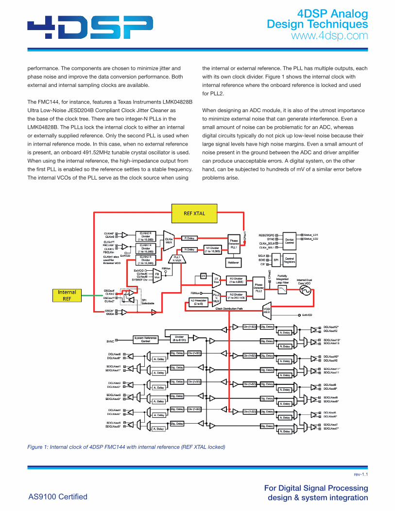
the internal or external reference. The PLL has multiple outputs, each
with its own clock divider. Figure 1 shows the internal clock with
internal reference where the onboard reference is locked and used
for PLL2.
When designing an ADC module, it is also of the utmost importance
to minimize external noise that can generate interference. Even a
small amount of noise can be problematic for an ADC, whereas
digital circuits typically do not pick up low-level noise because their
large signal levels have high noise margins. Even a small amount of
noise present in the ground between the ADC and driver amplifier
can produce unacceptable errors. A digital system, on the other
hand, can be subjected to hundreds of mV of a similar error before
problems arise.
performance. The components are chosen to minimize jitter and
phase noise and improve the data conversion performance. Both
external and internal sampling clocks are available.
The FMC144, for instance, features a Texas Instruments LMK04828B
Ultra Low-Noise JESD204B Compliant Clock Jitter Cleaner as
the base of the clock tree. There are two integer-N PLLs in the
LMK04828B. The PLLs lock the internal clock to either an internal
or externally supplied reference. Only the second PLL is used when
in internal reference mode. In this case, when no external reference
is present, an onboard 491.52MHz tunable crystal oscillator is used.
When using the internal reference, the high-impedance output from
the first PLL is enabled so the reference settles to a stable frequency.
The internal VCOs of the PLL serve as the clock source when using
4DSP Analog Design Techniques
Figure 1: Internal clock of 4DSP FMC144 with internal reference (REF XTAL locked)
AS9100 Certified
www.4dsp.com
For Digital Signal Processingdesign & system integration
Onderkant tussenkop op deze lijn
Onderkant kop op deze lijn
www en kader tot hier
rev-1.1
Determining the cause of external noise in an analog system and
eliminating it can be challenging, so it is best to be diligent during
the design phase to prevent noise issues before they arise. Careful
component selection is therefore a key step in creating a successful
circuit. Designing in a way that minimizes conducted noise can also
go a long way to reducing interference, but this is not always done
thoroughly for ADC/DAC products.
Degradation in signal-to-noise is caused largely by clock jitter, so it
is essential that the sampling clock add as little noise as possible
and has low phase jitter. This means using a low phase-noise voltage
controlled oscillator (VCO) to generate the sampling clock in a high-
performance analog signal digitizer because sampling clock jitter
raises the noise and distortion floor by modulating the analog input
signal. Care is also taken to isolate the sampling clock generator
from noise-producing digital circuits. The same is done for the op
amp and the ADC/DAC.
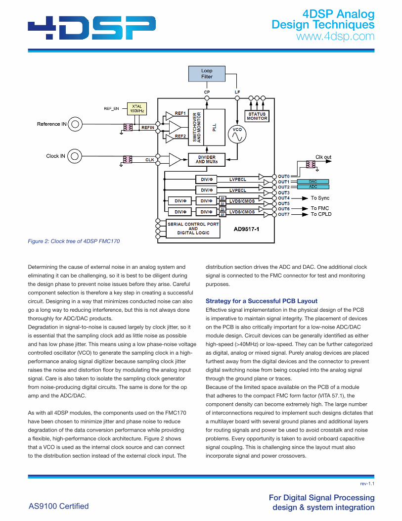
As with all 4DSP modules, the components used on the FMC170
have been chosen to minimize jitter and phase noise to reduce
degradation of the data conversion performance while providing
a flexible, high-performance clock architecture. Figure 2 shows
that a VCO is used as the internal clock source and can connect
to the distribution section instead of the external clock input. The
distribution section drives the ADC and DAC. One additional clock
signal is connected to the FMC connector for test and monitoring
purposes.
Strategy for a Successful PCB LayoutEffective signal implementation in the physical design of the PCB
is imperative to maintain signal integrity. The placement of devices
on the PCB is also critically important for a low-noise ADC/DAC
module design. Circuit devices can be generally identified as either
high-speed (>40MHz) or low-speed. They can be further categorized
as digital, analog or mixed signal. Purely analog devices are placed
furthest away from the digital devices and the connector to prevent
digital switching noise from being coupled into the analog signal
through the ground plane or traces.
Because of the limited space available on the PCB of a module
that adheres to the compact FMC form factor (VITA 57.1), the
component density can become extremely high. The large number
of interconnections required to implement such designs dictates that
a multilayer board with several ground planes and additional layers
for routing signals and power be used to avoid crosstalk and noise
problems. Every opportunity is taken to avoid onboard capacitive
signal coupling. This is challenging since the layout must also
incorporate signal and power crossovers.
Figure 2: Clock tree of 4DSP FMC170
4DSP Analog Design Techniques
AS9100 Certified
www.4dsp.com
For Digital Signal Processingdesign & system integration
Onderkant tussenkop op deze lijn
Onderkant kop op deze lijn
www en kader tot hier
rev-1.1
Traces on a PCB serve as transmission lines for high-speed boards,
and special care is taken by the layout engineer to optimize signal
integrity and deliver an efficient, high-performance ADC/DAC board
design. Maintaining separation between high-speed differential pair
traces is essential for signal integrity. Meanwhile, the inductance
and capacitance of traces determine the propagation delay, so the
width, thickness and shape of traces, as well as their distance from
the reference plane must be considered. Signal traces are also kept
as short as possible to minimize interference from onboard and
extraneous signals.
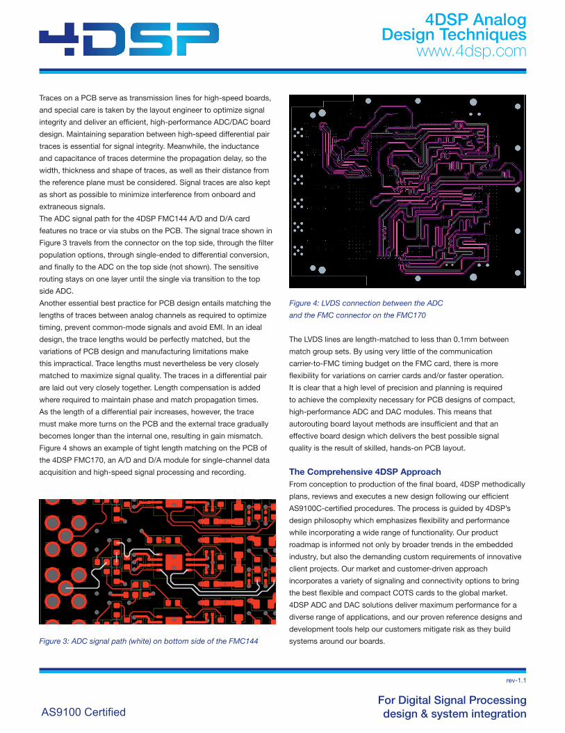
The ADC signal path for the 4DSP FMC144 A/D and D/A card
features no trace or via stubs on the PCB. The signal trace shown in
Figure 3 travels from the connector on the top side, through the filter
population options, through single-ended to differential conversion,
and finally to the ADC on the top side (not shown). The sensitive
routing stays on one layer until the single via transition to the top
side ADC.
Another essential best practice for PCB design entails matching the
lengths of traces between analog channels as required to optimize
timing, prevent common-mode signals and avoid EMI. In an ideal
design, the trace lengths would be perfectly matched, but the
variations of PCB design and manufacturing limitations make
this impractical. Trace lengths must nevertheless be very closely
matched to maximize signal quality. The traces in a differential pair
are laid out very closely together. Length compensation is added
where required to maintain phase and match propagation times.
As the length of a differential pair increases, however, the trace
must make more turns on the PCB and the external trace gradually
becomes longer than the internal one, resulting in gain mismatch.
Figure 4 shows an example of tight length matching on the PCB of
the 4DSP FMC170, an A/D and D/A module for single-channel data
acquisition and high-speed signal processing and recording.
The LVDS lines are length-matched to less than 0.1mm between
match group sets. By using very little of the communication
carrier-to-FMC timing budget on the FMC card, there is more
flexibility for variations on carrier cards and/or faster operation.
It is clear that a high level of precision and planning is required
to achieve the complexity necessary for PCB designs of compact,
high-performance ADC and DAC modules. This means that
autorouting board layout methods are insufficient and that an
effective board design which delivers the best possible signal
quality is the result of skilled, hands-on PCB layout.
The Comprehensive 4DSP ApproachFrom conception to production of the final board, 4DSP methodically
plans, reviews and executes a new design following our efficient
AS9100C-certified procedures. The process is guided by 4DSP’s
design philosophy which emphasizes flexibility and performance
while incorporating a wide range of functionality. Our product
roadmap is informed not only by broader trends in the embedded
industry, but also the demanding custom requirements of innovative
client projects. Our market and customer-driven approach
incorporates a variety of signaling and connectivity options to bring
the best flexible and compact COTS cards to the global market.
4DSP ADC and DAC solutions deliver maximum performance for a
diverse range of applications, and our proven reference designs and
development tools help our customers mitigate risk as they build
systems around our boards.
Figure 4: LVDS connection between the ADC
and the FMC connector on the FMC170
Figure 3: ADC signal path (white) on bottom side of the FMC144
4DSP Analog Design Techniques
AS9100 Certified