Embed Size (px)
Citation preview

한국산학기술학회논문지Vol. 11, No. 11 pp. 4121-4128, 2010
4121
Optimization of Thermal Deformation in Probe Card
Yong-Hoon Chang1, Jeong-Je Yin2* and Yong S. Suh3
1Department of Mechanical and Automotive Engineering, Induk University2Department of Mechanical Engineering Design, Induk University
3Department of Mechanical Engineering, California State University, Sacramento, USA
프로브 카드의 열변형 최적화
장용훈1, 인정제2*, Yong S. Suh31인덕대학 기계자동차과, 2인덕대학 기계설계과, 3CSU Sacramento 기계공학과
Abstract A probe card is used in testing semiconductor wafers. It must maintain a precise location tolerance for a fine pitch due to highly densified chips. However, high heat transferred from its lower chuck causes thermal deformations of the probe card. Vertical deformation due to the heat will bring contact problems to the pins in the probe card, while horizontal deformation will cause positional inaccuracies. Therefore, probe cards must be designed with proper materials and structures so that the thermal deformations are within allowable tolerances. In this paper, heat transfer analyses under realistic loading conditions are simulated using ANSYSTM
finite element analysis program. Thermal deformations are calculated based on steady-state temperature gradients, and an optimal structure of the probe card is proposed by adjusting a set of relevant design parameters so that the deformations are minimized.
요 약 프로브 카드는 웨이퍼의 칩 검사에 사용된다. 또한 반도체의 고집적화에 따른 미세피치 대응으로 높은 위치 정도가 요구된다. 그러나 실제 장비에서는 하부 척에서 높은 열이 프로브 카드로 전달되어, 프로브 카드의 열변형을 초래하게 된다. 프로브 카드의 수직방향 열변형은 핀의 접촉관련 문제를 야기할 것이고, 수평방향의 열변형은 x-y 방향으로의 위치 오차를 만들 것이다. 따라서 프로브 카드는 허용 범위내의 열변형이 이루어지도록 재질과 구조를 갖게 설계되어야 한다. 본 연구에서는 유한요소 해석프로그램인 ANSYSTM를 이용하여 프로브 카드의 실제 부하 조건들을 적용한 열전달 해석을 수행하였다. 정상상태 온도 구배에 대해 열변형이 계산되었으며, 최종적으로 적절한 설계변수들을 조정하여 열변형이 최소화 될 수 있는 새로운 구조를 제안하였다.
Key Words : Thermal Deformation, FEM, Probe Card
*Corresponding Author : Jeong-Je Yin([email protected])Received October 26, 2010 Revised November 17, 2010 Accepted November 19, 2010
1. Introduction
A probe card is an interface between a semiconductor wafer and testing equipment that checks the electronic characteristics of the semiconductor chips during the manufacturing process. A series of parallel pins on the printed circuit board (PCB) in the probe card makes physical contacts with the IC output pads, and it transfers the internal electronic characteristics to the external
testing equipment. A control system detects and removes any defect chips based on the signal characteristics it receives from the probe card. This reduces assembly and inspection time and improves the product yield rates.
Probe cards can be classified into different types based on the shapes of the contact elements. A vertical card[1,2] has tungsten wires sharpened to needles and assembled vertically, while a horizontal card has its wires bent and assembled horizontally. A MEMS card[3-5] is a vertical

한국산학기술학회논문지 제11권 제11호, 2010
4122
type made using the semiconductor process technology.
Higher density of integrated circuits reduces the I/O pad
pitch of the chips, limiting the space for the probe cards.
Hence, the horizontal type is replaced by the vertical type,
and then further developed to MEMS vertical type.
In designing a probe card, its positional accuracy is
getting more important because the pad pitch is smaller
while the wafer size is getting larger. The heat transferred
from the chuck under the probe card, however, develops
horizontal and vertical deviations of the probe pins during
the testing process. The vertical deviation causes contact
errors of the pins, and the positional accuracy of the pins
is affected by the horizontal deviation. Therefore, a proper
structural design and choice of materials are important so
that the deviations can be controlled and limited.
Related research experimentally shows that the thermal
deformations affect the accuracy of the probe cards[6].
Others studied on the relationships between the heat
distributions of the chuck and the thermal deformations of
the probe cards [7,8], and on the thermal deformations
due to the layered structure of the printed wiring board
(PWB)[9]. However, little research is found on the design
of probe cards based on the analyses of their thermal
deformations.
In this research, temperature distributions of a probe
card under a realistic testing environment are investigated
using a commercial finite element analysis package,
ANSYSTM
. Based on the thermal deformations through
the analyses of temperature distributions, an optimal
structure of a probe card that minimizes the thermal
deformations is proposed. Also, this paper reports useful
data for correcting the thermal deformations by analyzing
the deformations of the probe cards under the loads
applied to the pins in addition to the thermal
deformations.
2. Modeling of a Probe Card
A probe card is an assembly of many components as
shown in Fig. 1.
A test is performed after the bottom of the probe card
is in contact with the lower chuck at 125 °C with a gap
of 200 ㎛ for five minutes as shown in Fig. 2.
[Fig. 1] Exploded view of a probe card
[Fig. 2] Schematic diagram for probe card test[10]
Table 1 illustrates the mechanical and thermal
properties of the components in the probe cards used in
the analysis of the paper. Anisotropic property of the PCB
is considered.
[Table 1] Material properties of probe card parts
Part Material
Young's
modulus
E (GPa)
Conductance
(W/m*K)
Heat
capacity
(J/kg*K)
CTE
(K-1)
Ceramic AL2O3 167 88.5 831 13.2×10⁻⁶
Column A6061 68.9 154 896 23.6×10⁻⁶
Steel
plateSUS303 193 16.2 500 17.2×10⁻⁶
Stiffener S45C 205 49.8 486 11.5×10⁻⁶
PCB FR4x,y 16.9,
z 7.440.291 1,200
x,y
16.0×10⁻⁶
z 84.0×10⁻⁶
Hole
block
POLYI
MIDE4 0.35 1,200 54.0×10⁻⁶
- Air - 0.026 1,010 -
Fig. 3 shows the meshed probe card model for finite
element analyses. The empty space inside the probe card
Optimization of Thermal Deformation in Probe Card
4123
is also meshed in order to analyze the heat transfer
through the air. The air mesh is then removed in the
deformation analysis that follows the heat distribution
analysis.
[Fig. 3] Mesh model of the probe card for the finite
element analysis
3. Heat Transfer Analysis
Fig. 3 shows a finite element model using 10 node
tetra solid elements for a heat transfer analysis. Thermal
contact resistances among components are ignored. The
empty space inside the probe card is also meshed using
the same element type to analyze the heat transfer through
the air. Heat convection to the environment is also
considered assuming that the room temperature is at 25
°C.
Under the above conditions, a transient heat transfer
analysis is performed after five minutes have passed. The
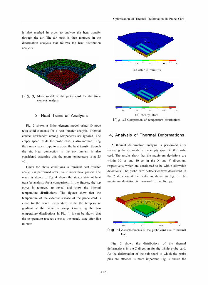
result is shown in Fig. 4 shows the steady state of heat
transfer analysis for a comparison. In the figures, the top
cover is removed to reveal and show the internal
temperature distributions. The figures show that the
temperature of the external surface of the probe card is
close to the room temperature while the temperature
gradient at the center is steep. Comparing the two
temperature distributions in Fig. 4, it can be shown that
the temperature reaches close to the steady state after five
minutes.
(a) after 5 minutes
(b) steady state
[Fig. 4] Comparison of temperature distributions
4. Analysis of Thermal Deformations
A thermal deformation analysis is performed after
removing the air mesh in the empty space in the probe
card. The results show that the maximum deviations are
within 50 ㎛ and 10 ㎛ in the X and Y directions
respectively, which are considered to be within allowable
deviations. The probe card deflects convex downward in
the Z direction at the center as shown in Fig. 5. The
maximum deviation is measured to be 160 ㎛.
[Fig. 5] Z-displacements of the probe card due to thermal
load
Fig. 5 shows the distributions of the thermal
deformations in the Z-direction for the whole probe card.
As the deformation of the sub-board to which the probe
pins are attached is more important, Fig. 6 shows the

한국산학기술학회논문지 제11권 제11호, 2010
4124
(a)
(b)
(c)
(d) (e)
(f)
[Fig. 7] Modification of internal structure for the reduction of thermal deformation (a) initial model, (b) add 2 columns,
(c) add 4 columns, (d) add 4 columns, increase thickness 2mm, (e) add 4 columns, increase thickness 2mm,
increase length 3mm, (f) add 4 columns, increase thickness 2mm, increase length 3mm, increase stiffener
thickness 3mm
Z-displacements of the sub-board due to heat. The
sub-board also deflects convex downward with the
maximum deformation of 103 ㎛.
[Fig. 6] Z-displacements of the sub-board due to thermal
load
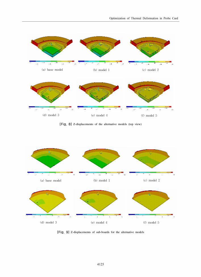
5. Optimization of Thermal Deformation
To minimize the deformations due to heat in the Z
direction, heat transfer and thermal deformation analyses
are performed on five alternative structural designs by
modifying the number of columns and their sizes as
summarized in Table 2. Fig. 7 illustrates the five
alternatives comparing with the initial model. Fig. 8
shows the Z-displacements of the alternative probe cards
after running thermal analyses.
Case No. of column
Column thickness
(mm)
Column length(mm)
Stiffener thickness
(mm)
Base model 4 4 88 12
Model 1 6 4 88 12
Model 2 8 4 88 12
Model 3 8 6 88 12
Model 4 8 6 91 12
Model 5 8 6 91 15
[Table 2] Design alternatives for the reduction of thermal
deformation
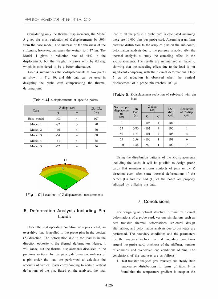
Fig. 9 shows the Z-displacements of the sub-boards of
which the deformations are considered to be the same as
those of the probe pins. In the figure, the thermal
displacements are reduced as the number of columns
increases as summarized in Table 3.
CaseTotal
weight(kg)
Weight change
(kg)
Weight increase
(%)
Max. Z-disp.
(㎛)
Deformation
reduction rate (%)
Base model 7.78 0.00 0.0 -103 0
Model 1 7.82 0.04 0.5 -87 16
Model 2 7.86 0.08 1.0 -66 36
Model 3 7.94 0.16 2.1 -64 38
Model 4 7.95 0.17 2.2 -61 41
Model 5 8.96 1.17 15.1 -52 50
[Table 3] Summary of thermal deformations
Optimization of Thermal Deformation in Probe Card
4125
(a) base model (b) model 1 (c) model 2
(d) model 3
(e) model 4
(f) model 5
[Fig. 8] Z-displacements of the alternative models (top view)
(a) base model (b) model 1 (c) model 2
(d) model 3
(e) model 4
(f) model 5
[Fig. 9] Z-displacements of sub-boards for the alternative models
한국산학기술학회논문지 제11권 제11호, 2010
4126
Considering only the thermal displacements, the Model
5 gives the most reduction of Z-displacements by 50%
from the base model. The increase of the thickness of the
stiffeners, however, increases the weight to 1.17 kg. The
Model 4 gives a reduction rate of 41% in the
displacement, but the weight increases only by 0.17kg,
which is considered to be a better alternative.
Table 4 summarizes the Z-displacements at two points
as shown in Fig. 10, and this data can be used in
designing the probe card compensating the thermal
deformations.
CaseZ-disp. (㎛) dZC-dZO
(㎛)O C
Base model -103 4 107
Model 1 -87 3 90
Model 2 -66 4 70
Model 3 -64 4 68
Model 4 -61 4 65
Model 5 -52 4 56
[Table 4] Z-displacements at specific points
O
C
O
C
[Fig. 10] Locations of Z-displacement measurements
6. Deformation Analysis Including Pin
Loads
Under the real operating condition of a probe card, an
over-drive load is applied to the probe pins in the vertical
(Z) direction. The deformation due to the load is in the
direction opposite to the thermal deformation. Hence, it
will cancel out the thermal displacements discussed in the
previous sections. In this paper, deformation analyses of
a pin under the load are performed to calculate the
amounts of vertical loads corresponding to certain vertical
deflections of the pin. Based on the analyses, the total
load to all the pins in a probe card is calculated assuming
there are 10,000 pins per probe card. Assuming a uniform
pressure distribution to the array of pins on the sub-board,
deformation analysis due to the pressure is added after the
thermal analysis to study the canceling effect in the
Z-displacements. The results are summarized in Table 5,
showing that the canceling effect due to the load is not
significant comparing with the thermal deformations. Only
7 ㎛ of reduction is observed when the vertical
displacement of a probe pin reaches 100 ㎛.
Normal pin displaceme
nt(㎛)
Pin load(g)
Z-disp.(㎛) dZC-
dZO
(㎛)
Reduction of Z-disp.
(㎛)O C
0 - -103 4 107 -
25 0.86 -102 4 106 1
50 1.73 -101 2 103 4
75 2.59 -100 1 101 6
100 3.46 -99 1 100 7
[Table 5] Z-displacement reduction of sub-board with pin
load
Using the distribution patterns of the Z-displacements
including the loads, it will be possible to design probe
cards that maintain uniform contacts of pins in the Z
direction even after some thermal deformations if the
center (O) and the end (C) of the board are properly
adjusted by utilizing the data.
7. Conclusions
For designing an optimal structure to minimize thermal
deformations of a probe card, various simulations such as
heat transfer, thermal deformations, structural design
alternatives, and deformation analysis due to pin loads are
performed. The boundary conditions and the parameters
for the analyses include thermal boundary conditions
around the probe card, thickness of the stiffener, number
of columns, and over-drive load conditions of pins. The
conclusions of the analyses are as follows:
1. Heat transfer analyses give transient and steady state
temperature distributions in terms of time. It is
found that the temperature gradient is steep at the
Optimization of Thermal Deformation in Probe Card
4127
center where heat dissipation is relatively low.
2. A method to minimize the thermal deformation of a
probe card using thermal deformation analyses is
demonstrated. The vertical deflection of probe pins
is an important indication of pin contacts and the
stability of the card. A new design is proposed so
that the vertical deflection is reduced by up to 50%.
3. The number and the thickness of the columns are
changed to minimize the thermal deformations. It
can be shown that the thermal deformations are
reduced significantly as the number of columns
increases. An optimal design is found to use eight
columns, each with 6 mm thickness, to minimize
the weight and the deformations.
4. Assuming a uniform pressure is applied to the array
of pins, deformation analyses due to the pressure are
added to investigate their canceling effect on the
Z-displacements of the probe pins due to the
thermal deformations.
References
[1] C.H. Min and T.S. Kim, "Development and
Characterization of Vertical Type Probe Card for
High Density Probing Test", Journal of the Korean
Institute of Electrical and Electronic Material
Engineers, Vol. 19, No. 9, pp. 825-831, September
2006.
[2] J.T. Chiu, D.Y. Chang, "A new probe design
combining finite element method and optimization
used for vertical probe card in wafer probing",
Precision Engineering, Volume 33, Issue 4,
pp.395-401, 2009.
[3] C.H. Min and T.S. Kim, "Development of 121
pins/mm^2 High Density Probe Card using
Micro-spring Architecture", Journal of the Korean
Institute of Electrical and Electronic Material
Engineers, Vol. 20, No. 9, pp. 749-755, September
2007.
[4] H.J. Lee, J.Y. Kim, S.J. Lee, H.J. Choi, K.S. Kim
and J.H. Kim, "Reliability Design of MEMS based
on the Physics of Failures by Stress & Surface
Force", Proceedings of the KSME Conference, pp.
1730-1733, 2007.
[5] S. Ha, D. Kim, B. Shin, M. Cho and C. Han,
"Assessment of Design and Mechanical Characteristics
of MEMS Probe Tip with Fine Pitch", Journal of the
Korea Academia-Industrial cooperation Society, Vol.
11, No. 4, pp. 1210-1215, 2010.
[6] R. Schwartz, "Probe Card Metrology: High
Temperature Testing of Probe Cards", IEEE
Semiconductor Wafer Test Workshop, 2002.
[7] S.S Lee, J.Y. Yun and M.K. Kim, "Surface Thermal
Deformation of 12 inch hot-cold chuck", Proceedings
of the Korean Society Of Semiconductor Equipment
Technology, pp. 207-211, 2003.
[8] Y. Joo, H. Shin and M.K. Kang, "A Study of
Improvement of Low Temperature Uniformity of
Wafer Prober Chuck", Journal of the Korea
Academia-Industrial cooperation Society Vol. 10, No.
10, pp. 2572-2576, 2009.
[9] H.S. Lee, "Thermophysical Properties of PWB for
Microelectronic Packages with Solder Resist Coating
Process", Journal of the Microelectronics & Packaging
Society, Vol. 10, No. 3, pp. 73-82, 2003.
[10] Gunther Boehm, "Prober Stability with Large
Probing Area and High Pin count", 2006 SWTW
(South West Test Workshop)
Yong-Hoon Chang [Regular member]
• Feb. 1988 : M.S. Department
of Mechanical Engineering,
Sungkyunkwan University
• Apr. 1997 : Ph.D. Department
of Mechanical Engineering,
University of Florida, USA
• May. 1997 ~ Aug. 1999 :
Senior Researcher, Samsung
Aerospace Industries, LTD.
• Aug. 1999 ~ Current : Associate Professor, Department
of Mechanical and Automotive Engineering, Induk
University

한국산학기술학회논문지 제11권 제11호, 2010
4128
Jeong-Je Yin [Regular member]
• Aug. 1992 : Ph.D. Department
of Mechanical Design &
Production Engineering, Seoul
National University
• Jan. 1993 ~ Apr. 1995 : Senior
Researcher, Korea Automotive
Technology Institute
• May. 1995 ~ Aug. 1999 :
Principal Researcher, Institute
for Advanced Engineering
• Aug. 1999 ~ Current : Associate Professor, Department
of Mechanical Engineering Design, Induk University
Yong S. Suh [Regular member]
• Nov. 1995 : Ph.D. Department
of Mechanical Engineering,
Rensselaer Polytechnic Institute
(RPI), USA
• Nov. 1995 ~ Jul. 1998 :
Structural Dynamics Research
Corporation (SDRC), USA
• Aug. 1998 - Nov 2003 :
SolidWorks Corporation, USA
• Jan. 2004 ~ Current : Associate Professor,
Department of Mechanical Engineering, California
State University, Sacramento, USA


![Mise en page 1 · ENVYVIN]KWPNK SFWFJPN • Satelec® С5),7?,44A0 /4897:3,49 Rus 210x297_chirurgie_tips_RUS.qxd 15.8.08 18:08 Page 1](https://img.pdfslide.tips/doc/110x75/5fd4c5ebe9922e2989251118/mise-en-page-1-envyvinkwpnk-sfwfjpn-a-satelec-5744a0-4897349-rus-210x297chirurgietipsrusqxd.jpg)