Embed Size (px)
Citation preview

UPTEC K13017
Examensarbete 30 hpAugusti 2013
Organic-inorganic hybrid perovskites as light absorbing/hole conducting material in solar cells
Saman Ghanavi

Teknisk- naturvetenskaplig fakultet UTH-enheten Besöksadress: Ångströmlaboratoriet Lägerhyddsvägen 1 Hus 4, Plan 0 Postadress: Box 536 751 21 Uppsala Telefon: 018 – 471 30 03 Telefax: 018 – 471 30 00 Hemsida: http://www.teknat.uu.se/student
Abstract
Organic-inorganic hybrid perovskites as lightabsorbing/hole conducting material in solar cells
Saman Ghanavi
Solar cells involving two different perovskites were manufactured and analyzed. Theperovskites were (CH3NH3)PbI3 and (CH3NH3)SnI3. Both perovskites have ashared methyl ammonium group (MA) and are used as both light absorbing materialand hole conducting material (HTM) in this project. The preparation procedures forthe complete device were according to previous attempts to make stableorganic-inorganic hybrid perovskites and involved different layers and procedures. Both perovskites were manufactured by mixing methyl ammonium iodide with eitherlead iodide or tin iodide in different concentrations. This was then deposited on a600nm thick mesoporous TiO2 layer. Deposition of the hole-transporting material(HTM) was done by spin-coating 2,2´,7,7´-tetrakis-(N,N-dip-methoxyphenylamine)9,9´-spirobifluorene, also called spiro-OMeTAD. Lastly thermal evaporation was usedto deposit a silver electrode.Different measurements were done on the light absorbing materials. The leadperovskite solar cell device was subjected to illumination with Air Mass 1.5 sunlight(100mW/cm2) which produced an open circuit voltage Voc of 0.645 V, a short circuitphotocurrent Jsc of about 7 mA/cm2, and a fill factor FF of 0.445. This resulted in apower conversion efficiency (PCE) of about 2% and an incident photon to currentefficiency (IPCE) of up to 60%. The tin perovskite has not been used in solar cells before and the initial resultspresented here shows low performance using the same device construction as for thelead perovskite. However, the incident photon to electron conversion affirms thatthere is a current in the visible region, and IPCE of 12.5 % was observed at 375nm.UV-visible NIR measurement was used to analyze the light absorption of theperovskite structures and a broader light absorption was observed for the leadperovskite compared to the tin perovskite.X-ray diffraction (XRD) analyzing was done on both perovskite materials usingdifferent concentrations and both with and without nanoporous TiO2 film. Bothperovskites demonstrate very similar peaks with some exceptions.Photo-induced absorption (PIA) measurement was used for the purpose of showingthe magnitude of charge separation or hole transfer in the light absorbing material,both when using the perovskites as a light absorber and a hole conductor. This ismeasured by analyzing the hole injection from the excited light absorber into theHTM. Hole transfer was observed for the lead perovskite (when used as lightabsorber) and tin perovskite (when used as hole conductor).
ISSN: 1650-8297, UPTEC K13 017Examinator: Karin LarssonÄmnesgranskare: Gerrit BoschlooHandledare: Erik Johansson
Master Thesis 30 hp vt 2013
Organic-inorganic hybrid perovskites as light absorbing/hole conducting material in
solar cells Saman ghanavi
1
1. Abstract
Solar cells involving two different perovskites were manufactured and analyzed. The
perovskites were (CH3NH3)PbI3 and (CH3NH3)SnI3. Both perovskites have a shared methyl
ammonium group (MA) and are used as both light absorbing material and hole conducting
material (HTM) in this project. The preparation procedures for the complete device were
according to previous attempts to make stable organic-inorganic hybrid perovskites and
involved different layers and procedures.
Both perovskites were manufactured by mixing methyl ammonium iodide with either lead
iodide or tin iodide in different concentrations. This was then deposited on a 600nm thick
mesoporous TiO2 layer. Deposition of the hole-transporting material (HTM) was done by
spin-coating 2,2´,7,7´-tetrakis-(N,N-dip-methoxyphenylamine) 9,9´-spirobifluorene, also
called spiro-OMeTAD. Lastly thermal evaporation was used to deposit a silver electrode.
Different measurements were done on the light absorbing materials. The lead perovskite solar
cell device was subjected to illumination with Air Mass 1.5 sunlight (100mW/cm2) which
produced an open circuit voltage Voc of 0.645 V, a short circuit photocurrent Jsc of about 7
mA/cm2, and a fill factor FF of 0.445. This resulted in a power conversion efficiency (PCE) of
about 2% and an incident photon to current efficiency (IPCE) of up to 60%.
The tin perovskite has not been used in solar cells before and the initial results presented here
shows low performance using the same device construction as for the lead perovskite.
However, the incident photon to electron conversion affirms that there is a current in the
visible region, and IPCE of 12.5 % was observed at 375nm.
UV-visible NIR measurement was used to analyze the light absorption of the perovskite
structures and a broader light absorption was observed for the lead perovskite compared to the
tin perovskite.
X-ray diffraction (XRD) analyzing was done on both perovskite materials using different
concentrations and both with and without nanoporous TiO2 film. Both perovskites
demonstrate very similar peaks with some exceptions.
Photo-induced absorption (PIA) measurement was used for the purpose of showing the
magnitude of charge separation or hole transfer in the light absorbing material, both when
using the perovskites as a light absorber and a hole conductor. This is measured by analyzing
the hole injection from the excited light absorber into the HTM. Hole transfer was observed
for the lead perovskite (when used as light absorber) and tin perovskite (when used as hole
conductor).
2

2. Populärvetenskaplig sammanfattning -Organisk-oorganisk perovskit som ljusabsorberande/håltransporterande material i solceller Denna master tes syftar till att få en större förståelse för grunderna i solcellsingenjörskunskap
och utförs i fysikaliska kemi institutionen på Ångströms laboratoriet.
Det finns en ständigt ökande törst för energi bland många utvecklingsländer. Deras
ekonomier växer explosionsartat i en takt ej skådad i mänsklighetens historia. Många länder
vänder sina ögon till billigare energi utan att ta hänsyn till de enorma negativa konsekvenser
det innebär för miljön och hållbarheten i den valda energin. Allt detta ger oss en känsla av att
vi måste påskynda arbetet med övergången till förnybara energikällor som vind, vågor,
jordvärme, biobränsle och sist men inte minst solenergi.
År 2002 fanns det mer energi på en timmes solljus som absorberas av jorden än hela världens
energiförbrukning under ett år. Solenergi har många fördelar och nackdelar. En av de stora
fördelarna med att använda solceller för att generera elektricitet är att det är miljövänligt
vilket inte är fallet för de flesta fossila bränslen. Den enda föroreningen som solceller skapar
är under själva tillverkningsprocessen av solcellsenheten. En annan stor fördel är förmågan att
generera el på platser som inte är kopplade till ett elnät, som i små byar eller till satelliter.
Men det finns också en del negativa aspekter som forskarna försöker lösa, och det är den höga
tillverkningskostnaden och alltför låg effektivitet. Kiselsolceller är den mest utbredda
solcellen på marknaden och har en effektivitet på mellan 10% och 20%. I dagsläget kräver
tillverkningen en alltför hög kostnad. Därför utforskar om andra material kan användas istället
som ljusabsorberande del i solcellen.
Syftet med detta projekt var att undersöka solceller baserade på nanopartiklar av TiO2 och ett
ljusabsorberande perovskitmaterial. Det har nyligen visat sig resultera i effektiva solceller.
Under projektets gång studerades flera framställningssteg av perovskitmaterial och även
beredning av den fullständiga solcellen, inklusive spray-pyrolys av TiO2, spinnbelägga
nanopartiklar av TiO2 och perovskit. Slutligen gjordes en deponering av en organisk hålledare
och silver kontakt genom termisk förångning. Efteråt byttes perovskiten, CH NH PbI
(MAPbI ) ut mot CH NH SnI (MASnI ) dvs ett annat
3 3 3
3 3 3 3 3 perovskitmaterial för att se ifall
effektiviteten kunde höjas
.
3

Olika analysmetoder användes för att se skillnaden i egenskaperna hos dessa två perovskiter.
Proverna analyserades med hjälp av UV-vis spektroskopi för att se skillnad i ljusabsorption
och kristallstrukturen karakteriserades med röntgendiffraktion. IPCE mätningar användes för
att undersöka foton till ström konverteringen i olika våglängder och PEC mätningar gjordes
för att mäta effektiviteten av solcellerna. Stabiliteten hos solcellerna och perovskit materialen
studerades med hjälp av en Ar glovebox för kontrollerad atmosfär och jämfördes till
atmosfäriska standardförhållanden.
Slutligen studerades effekten av att använda (MASnI ) perovskit3 som hålledare i stället för
det ljusabsorberande materialet.
Resultaten visade prov på en relativt hög effektivitet på 2% för (MAPbI ) solcellerna, och
0.002 % effektivitet för (MASnI ).
3
3
4

Table of Contents Page
1. Abstract 2
2. Populärvetenskaplig sammanfattning 3
3. Introduction 6
4. Aim 7
5. Chemistry behind solar cell functionality 8
6. Theory 10
7. Experimental part 1 15
8. Results part 1 21
9. Experimental part 2 29
10. Results part 2 31
11. Conclusions 34
12. Discussion and Future prospects 35
13. Acknowledgments 36
14. References 36
15. Appendix 37
5

3. Introduction
The ever increasing thirst for energy is something that cannot be neglected. Many developing
countries are growing their economies at a pace not seen in human history. The growing
economies are a result of human desire to always improve their living standards. Many
countries turn their eyes to cheap energy not taking into consideration the huge negative
repercussions for the environment. Another factor not taken into consideration is the
sustainability of that energy, for example oil production is estimated to have reached its peak
extraction capability in the 1980s in the US and is on the decline. It is widely known that the
amount of crude oil being extracted from the soil is directly dependent on the amount of
investment made, so if the right investments is not made the productivity will decrease over
time and indirectly increase the energy price[1]. All this gives us a sense that we must
accelerate the effort to transition to renewable energies such as wind, rain, tides, waves,
geothermal heat, biofuels and last but not least solar energy.
The sun emits ultraviolet, visible and infrared light. The sunlight is reflected by the ozone
layer, atmosphere, clouds and particles in the air. A total of 120TW solar energy approaches
earth but only a fraction is absorbed by the land and oceans the rest is reflected out in the
space by the atmosphere. In 2002, there was more energy in one hour sunlight absorbed by
the earth than the whole world energy consumption in a whole year. If only a small bit of this
huge energy pool would be captured by solar cells that would certainly put an end to energy
thirst around the globe and constitute a energy revolution not observed ever before in human
history not even the industrialization in the 1700s[2]. Solar energy has many advantages but less disadvantages. One of the huge advantages of
using solar cells for generating electricity is that it's environmentally friendly which is not the
case for most fossil fuels. The only pollution that solar cells create is during the
manufacturing of the solar cell device. Another great advantage is the capacity to generate
electricity at places that are not linked to an electricity grid, like in small villages or even
space satellites. But there are also some negative aspects that scientists are trying to
overcome, is the high manufacturing cost and too low efficiencies. Silicon solar cells are the
most widespread solar cells on the market and are between 10% and 20% efficient. Therefore
other materials for the light absorbing part of the solar cell needs to be examined to acquire
higher efficiencies and lowering costs.
6

4. Aim
The aim of this project is to obtain a greater understanding for the basics of solar cell
engineering. In this project one is to investigate solar cells based on nanoparticles of TiO2
and a light absorbing perovskite material. It has recently been shown to result in efficient
solar cells, hence the project will start by preparing similar solar cells. This includes several
preparation steps of the perovskite material and also preparation of the complete solar cell,
including spray pyrolysis of TiO2, spin-coating nanoparticles of TiO2, depositing the
perovskite by spin-coating, depositing an organic hole-conductor and a silver contact by
thermal evaporation. After learning how to prepare these solar cells using the perovskite, CH3
NH3PbI3, one will try another perovskite material. The Pb in the perovskite will be exchanged
to Sn, and the difference in properties of these two perovskites will be analyzed using UV-vis
spectroscopy and XRD. Also compare the Sn based perovskite and the Pb perovskite in the
solar cell, and make IPCE and PEC measurements. The stability of the solar cells and the
perovskite materials will be studied using an argon glove box for controlled atmosphere and
compare these experiments to standard atmospheric conditions.
Finally study the effect of using (CH3NH3)SnI3 perovskite as a hole conductor instead of the
light absorbing material.
7

5. Chemistry behind solar cell functionality
The main procedures in a DSC or perovskite solar cells that determines if the solar cell works
or the efficiency of the solar cell are light absorption by the light absorber material, charge
separation to prevent recombination inside the light absorber, electron injection to the TiO2,
charge collection at both the TiO2 and HTM interface and lastly light absorber regeneration.
When the light absorbing material in the solar cell is illuminated subsequently an electron is
excited from the HOMO to the LUMO energy level. The electron is injected to the conduction
band of the nanoporousTiO2, and the hole created is transferred to the hole transporting
material. The regeneration of the oxidized light absorbing material depends on both the
energy levels of the valence bands of both the light absorbing material and hole transporting
material. The energy levels of the tin based perovskites are unknown, therefore it isn´t known
if the electrons and holes are spontaneously transferred, thereby the figure 1 is not necessarily
correct.
Figure 1. Schematic picture of the energy levels in a solar cell[4]
8

The current of the solar cell is determined by the absorption spectra of
the light absorber.
To get a higher efficiency of the solar cell one has to increase the surface area between the
semiconductor and the light absorber. That is why the semiconductor metal oxide usually
used (TiO2) is nanoporous so the light absorbing material can infiltrate into the pores[3].
9

6. Theory: characterization techniques Current-voltage measurement
The power conversion efficiency (PCE) of solar cells is evaluated by measuring the power it
produces while exposed to illumination at 1.5AM (100mW/cm2) which is 1 sun illumination.
The I-V measurement is done under sunlight by varying the voltage.
A typical I-V measurement result is shown in figure 2.
Figure 2. Typical I-V measurement. Important parameters are found.
The maximum point of the product between the current and voltage, the maximum power
(Pmax) is established[3].
Power conversion efficiency of solar cells is described by the ratio between the Pmax and Pin:
η=Pmax/Pin=FF×Jsc×Voc/Pin (eq. nr 1)
Voc: open circuit voltage
Jsc: short circuit current
FF: fill factor
Pin: incident power
To obtain a higher PCE the Voc, Jsc and FF needs to increase while at the same time the Pin
needs to decrease[5].
10

Incident photon to current conversion efficiency measurement
The incident-photon to current conversion efficiency (IPCE) investigate the efficiency of
converting light of a specific wavelength to electrons and current.
Incident-photon-to-current efficiency, is used to analyze how many electrons is created by
each photon sent from the light source which is of a high importance to obtain high efficiency
solar cells. These measurements are performed under standard illumination 1.5AM
(100mW/cm2). The IPCE setup was calibrated with a silicon diode prior to usage.
For solar cells to be highly efficient and competitive in the market they need to have a large
IPCE in all wavelengths but most importantly in the red to near infrared regions since sunlight
radiation is quite high in these wavelengths.
The IPCE spectrum gives a sense of the light response of the device in mind and is connected
to the short circuit current (Jsc).
The parameters that determine the performance of solar cells has been identified as light
absorption by the light absorber material, charge separation to prevent recombination inside
the light absorber, electron injection to the TiO2, charge collection at both the TiO2 and HTM
interface and lastly light absorber regeneration. The IPCE addresses all these parameters since
it is determined by them[3].
IPCE = LHE×injection×regeneration×charge collection (eq. nr 2)
Ultraviolet–visible spectroscopy NIR
Ultraviolet-Visible NIR spectroscopy (UV-vis NIR) was performed to analyze the light
absorption of both perovskites, and the spectra were recorded on a HR-2000 Ocean optics
spectrophotometer.
In a DSC or perovskite solar cells one of the factors determining if the solar cell works is the
light absorption by the light absorber material. That is why UV-vis is of great importance.
Absorptions spectra was examined using regular ultraviolet-visible light for wavelengths up to
1100nm.
What happens inside the sample when performing UV-vis NIR is that when the sample is
illuminated with light an electron is excited corresponding to the energy difference between
an electronic transition( for example bonding to anti-bonding) inside the molecules. The light
is absorbed and the absorption of the sample is shown as a graph at different wavelengths. [6]
11

Photo-induced absorption spectroscopy
In this project photo induced absorption spectroscopy (PIA) also referred to as "pump probe
method" is used to investigate the processes for charge generation and hole transfer in both
lead and tin based perovskites. This gives an idea on how well the hole is transported
depending on how large the peaks are in the spectra. PIA is used in this case to measure the
change in absorption both with and without adding HTM.
A pulsed light beam of 530nm green light emitted by a laser LED in this case excites the
sample constituting a complete solar cell device (described in the experimental part) without
the Ag counter electrode. Then the white "probe light" beam analyzes the excited sample. The
light is sent through the sample to the monochromator and detection occurs using either a Si
or Ge photodiode, for visible and IR-regions, respectively. The signal is analyzed using a
computer (see figure 3) [7].
Figure 3. Demonstration of functional parts in a photo-induced absorptions instrument
X-ray diffraction
In this project the X-ray diffraction(XRD) is used to study the lead and tin perovskite to
examine the structure and confirm that what is obtained is a perovskite and not something
else. A thin film D5000 Siemens XRD instrument was used and X-rays are generated when
focused electrons are accelerated with a high-voltage field and bombards the sample[8].
12

When a focused X-ray beam interacts with these planes of atoms, part of the beam becomes
scattered radiation which in turn forms patterns (diffraction patterns) that is related to the
structure of the material. Both directions of the scattered rays and their intensities provide
important knowledge of the perovskite.
Bragg's law is used to determine the angles that give rise to constructive interference(figure
4), in other words, angles with strong scattering [9].
2dsinθ = λ (eq 1)
where θ is the angle between the incident beam and lattice plane, λ is the wavelength of the
X-rays.
Figure 4. Constructive interference through the material
Scanning electron microscope
SEM is a useful technology applied in many different fields and is commonly used in
industrial companies and universities.
A scanning electron microscope (SEM) is a kind of an electron microscope. The electrons that
is emitted from the electron gun interact with the atoms in the solar cell and subsequently
generate signals regarding the cells surface topography [10].
13

When the electron beam hits the sample, varying signals
emerge (secondary electrons, X-rays, back scattered
electrons. The back scattered electrons gives chemical
information, while secondary electrons give topographic
information.
This SEM analysis requires vacuum and a non-conductive
sample is more difficult to study because it becomes charged
when the electron beam hits it[11].
Figure 5. Functional parts of SEM[12]
Figure 5 shows the entire sequence of events from the electron beam is shoot out, until the
beam hits the sample, and finally the received secondary electrons are analyzed in a detector
and the result is displayed [12].
In this project a Zweiss 1550 scanning electron microscope was used to examine the cross
section and topography of the solar cell device. This gives valuable information about the
different layers, most of all to see if the light absorber has infiltrated the TiO pores. 2
14

7. Experimental part 1
To manufacture a perovskite solar cell one has to go through several processes, such as
cutting, washing, etching, annealing, spray pyrolysis of underlayer. And then spin coating of
TiO2, perovskite and the hole transporting material (HTM). Finally to get a full working solar
cell one must do a deposition of a counter electrode, in this case silver, on top of the HTM.
The preparation procedure is described in detail below.
Preparation of glass substrates
Cutting glass: 24x30mm cuts on the conducting side of the glass. How the cutting takes place
is observed in figure 6.
Figure 6. Schematic picture on how to cut the glass
Several washing steps of the substrates is needed to get them cleaned. Put them in a beaker
with some water and RBS-solution. Refill with only water. Sonicate after each washing step
for 30 min. Then dry the substrates using airflow.
The etching of the FTO takes place to try to prevent a short circuit in the complete solar cell
device. While etching one can use a table with millimeter-marks to put some scotch tape on,
covering about 11mm on each side of the glass substrates(put the tape on the conducting
side). Add some zinc in between the two tapes, where there is no tape covered. Then add the
2M HCl(aq) on the zinc using a pipette, until one obtain a bubbely effect (see figure 7).
15

Figure 7. The etching setup
After the bubbles have settled rinse off the zinc and HCl with some deionized water. Take
away the tape and wash with water and ethanol. Afterwards put the glass substrates in a
beaker filled with RBS-solution and water, and subsequently in pure water, in acetone and
finally in ethanol.
Underlayer treatment
Mix a solution of titanium isopropoxide, acetylacetone and ethanol 1:3:12 by volume in an
Erlenmeyer flask.
Put the glass samples in a row on a hot plate surface. Make a holder for it (see figure 8).
Warm the glass substrates slowly up to 550°C and wait for atleast 3h. Spray on the underlayer
water 20 times using the spray pyrolysis equipment and let the heating on 550°C remain for a
further 30 minutes. Then let the substrates cool down for approximately 1.5h.
16

Figure 8. Setup for the underlayer treatment.
TiO2 deposition
Prepare the TiO2 paste by mixing 1g of TiO2, 2.0g terpienol and 2.0g ethanol. Sonicate
several times to get a homogenous solution.
The TiO2 can be put on the glass substrates by either a "doctor blade"-method or spin coating,
but since a thickness of less than 1μm is sought the spin coating process was chosen.
The TiO2 paste was deposited by spin coating at 1000rpm for 9s, and 2500rpm for 30s. Then
for the annealing process put the glass substrates on a hotplate at 550°C for 3h.
TiCl4 treatment
Mix 1.2ml TiCl4 and 60ml water in a beaker and place the glass substrates in it. Put the beaker
then in a Fermaks oven at 70°C for 30 minutes.
Afterwards, take the glass substrates out, rinse with water and dry them using air.
Annealing takes place for approximately 2h at 550°C.
17

Preparation of MAPbI3 perovskite
In this project several different concentrations and molar ratios were examined, but only the
equimolar ratio solution is described in this part for simplicity.
Preparation of the equimolar ratio lead based perovskite sensitizer ((CH3NH3)PbI3) is done
by mixing 27.8ml methylamine(40wt% in methanol, TCI) with 30ml hydroidic acid(57wt%
water) in a 250ml round bottomed flask and stirred at 0°C(ice bath) for 2h. The solution was
then evaporated at 50°C for 1h under vacuum using an evaporator apparatus which resulted
in a white powder called methyl ammonium iodide (CH
in
3NH3I). The precipitate was washed
with diethyl ether several times.
To make the equimolar ratio lead based perovskite CH3NH3PbI3, mix CH3NH3I(1.96g) and
PbI2(5.72g, 99%), corresponding to 0.0123 moles of each reactant. Then one can either add
about 10ml of γ-butyrolactone(Sigma Aldrich, purity level>99%) or a mixture containing 8:2
v/v of γ-butyrolactone:DMF(Sigma Aldrich, purity level 99.8%). After complete dissociation
of the reactants, the solution can be purged with nitrogen flow for a couple of minutes. The
small beaker is immediately sealed and kept at dark at room temperature. Put Al-foil around
the sample to prevent reaction with sun light.
Filter the perovskite solution with two filters: a 13mm (filters the larger particles) and 0.45μm
(filters the smaller particles). If one may not have in possession one of the filters, using
centrifugation(4200rpm and 5 minutes) is also possible to separate the bigger particles [13].
When depositing the perovskite on the TiO2 layer of the glass substrate, use spin coating:
1000rpm for 9s and 2500rpm for 30s to obtain a fine layer. About 50μl perovskite solution per
glass substrate is a sufficient amount. Place the substrates on a hotplate at 100°C for 15
minutes.
Preparation of MASnI3 perovskite
The purpose of this project is to see if tin based perovskites is usable in solar cells. So instead
of using the lead based perovskite one can change it to a tin based perovskite.
The methyl ammonium iodide (CH3NH3I) was made as previously. To make the final tin
based perovskite pour the right amount of solvent γ-butyrolactone(20wt%) , metal compound
(SnI2) and methyl ammonium iodide in a beaker to obtain desired concentration. Seal the lid
with parafilm to avoid moisture[14].
18

It is important not to filter the tin perovskite or subject it to air as it immediately changes
coloration from yellow to black green. The change in color happens most probably due to
oxidation.
When depositing the tin based perovskite the same spin coating rate as for the lead perovskite
was used.
Spiro-OMeTAD deposition
Firstly one has to prepare the hole transporting material which in this case is spiro-OMeTAD.
Mix the chlorobenzene with TBP, Li-TFSI and spiro-OMeTAD.
Spin coat the glass substrates with the HTM-solution at 1000rpm for 9s and 4000rpm for 30s.
Note that how much HTM-solution you put on the glass substrate doesn’t affect the layer
thickness but rather the spin coating rate does[13].
Dry the samples on a hotplate at 150°C for 15 minutes and clean up the HTM from the
conducting surface using acetonitrile or more primitively a knife.
Silver deposition
Silver deposition is performed to create an electrode and a counter electrode to obtain a circuit
in which the electrons and holes can stream through the solar cell to obtain a current.
The deposition of silver were performed by thermal evaporation in vacuum (<810-5 mbar).
The deposition rate was kept between 0.2-0.5nm/s.
19

Complete solar cell
a) b)
Figure 9. a)cross-sectional animated complete solar cell device b) solar cell device from
above.
Etching of the FTO takes place to try to prevent a short circuit. In figure 9a one can see the
complete solar cell and also see the charge generation and transport.
Figure 9b shows a complete solar cell from above. This particular solar cell is the tin based
perovskite solar cell as hole conducting material.
20

8. Results part 1
Current-voltage and Incident photon to electron conversion efficiency
of MAPbI3 perovskite
Figure 10. Photovoltaic performances of equimolar ratio (CH3NH3) PbI3 (1M) perovskite
sensitized solar cell. (a) Photocurrent density as a function of the forward bias voltage. (b)
IPCE as function of incident wavelength.
The lead perovskite solar cell device was subjected to illumination with Air Mass1.5 sunlight
which produced an open circuit voltage Voc of 0.645 V, a short circuit photocurrent Jsc of
about 7 mA/cm2, and a fill factor FF of 0.445. This resulted in a PCE of about 2% and an
IPCE of up to 60% at 450nm(see figure 10). The parameter bringing the power conversion
efficiency down is the rather low fill factor of 0.445.
The photocurrent at 7mA/cm2 for the lead perovskite solar cell demonstrates efficient charge
generation and charge transport of both electrons and holes.
21

UV-visible NIR of MAPbI3 perovskite
Figure 11. UV-vis absorption spectra of different MAPbI3 perovskite concentrations. FTO
used as reference.
In figure 11 an absorptions spectra can be observed, not showing significant change in light
absorption with increasing concentration of the lead perovskite.
Figure 12. UV-vis absorption spectra of different MAPbI3 perovskite concentrations with
TiO2 (TiO2 used as reference)
As seen in figure 12 the TiO2 peak is observed at around 300 nm. The MAPbI3 peak is seen at
around 400 nm. The UV-vis spectra has changed dramatically compared to the samples
without TiO2 in the previous figure, leaving the conclusion that TiO2 enhances the light
absorption of MAPbI3 from 350nm up to around 900 nm. Observe that the lack of sunlight
22

absorption in the visible and near infrared regions has been an issue for dyes containing
ruthenium, which is one of the more used dyes currently used[4].
Another observation is that two small peaks emerge at around 500nm and 700nm. These small
peaks tend to increase with increasing concentration of the MAPbI3.
Photo-induced absorption MAPbI3 perovskite A photo-induced absorptions spectrum was performed of a equimolar ratio (CH3NH3) PbI3
(1M). The structure of the device examined in the PIA was the same as a complete solar cell
but without silver electrodes.
Figure 13. A photo-induced absorptions spectrum of equimolar ratio MAPbI3 (1M) perovskite.
In figure 13 one can see a bleaching of the ground state MAPbI3 perovskite at about 500nm.
No signal is obtained for the MAPbI3 perovskite without HTM, but with HTM a peak ranging
from about 1170-1430nm corresponding to oxidized spiro-OMETAD can be observed, thus
23

indicating that hole transfer is taking place from the MAPbI3 perovskite to the spiro-
OMETAD[15].
.
Current-voltage and Incident photon to electron conversion efficiency
MASnI3 perovskite
Figure 14. Photovoltaic performances of equimolar ratio (CH3NH3)SnI3 (1M) perovskite
sensitized solar cell. (a) Photocurrent density as a function of the forward bias voltage. (b)
IPCE as function of incident wavelength
The equimolar ratio (CH3NH3) SnI3 (1M) perovskite solar cell device were subjected to
illumination with Air Mass1.5 sunlight which at most produced an open circuit voltage Voc of
0.080 V, a short circuit photocurrent Jsc of about 0,068 mA/cm2, and a fill factor FF of 0.431.
This resulted in a power conversion efficiency (PCE) of 0,002% and an incident photon to
current efficiency (IPCE) of 0%(see figure 14) .
24

UV-visible MASnI3 perovskite
Figure 15. UV-vis absorption spectra of different tin perovskite concentrations with and
without TiO2 (TiO2 used as reference).
In figure 15 a small peak at around 390nm is observed for the sample with TiO2, indicating a
rather small increase in light absorption. The important thing regarding this spectra is that the
3:1 molar ratio MASnI3 (0.25M) has a significantly higher absorption than all the other
equimolar perovskites even without the TiO2.
Photo-induced absorption MASnI3 perovskite
Figure 16. A photo-induced absorptions spectrum of equimolar ratio (CH3NH3) SnI3 (1M)
perovskite.
25

In figure 16 no significant peak can be observed in this wavelength interval indicating no
hole-transfer has occurred from the perovskite to the hole transporting material which in this
case was spiro-OMeTAD. A sample containing equimolar ratio (CH3NH3) SnI3 (1M)
without spiro-OMeTAD was examined with the same result, no hole transfer[15].
The observations were done using both silicon and germanium detectors.
X ray-diffraction
XRD experiments were done using CuKα-radiation and obtained detailed data about
orientation and structure of the specified sample being examined. This can especially be seen
by comparing the (hkl) peaks and to see which ones are more distinct.
The experimental conditions for the XRD measurments were theta : 1, scan speed : 2 and
increment : 0.02. Scan angle : 15 to 70 degrees and the scan type set at unlocked coupled.
Figure 17. XRD-comparison of different concentrations and molar ratios of MASnI3 and
MAPbI3.
26

As one can see in figure 17 the peaks are pretty similar comparing the tin and lead based
perovskites to each other. What is mostly different is the intensity of the peaks, but one can
also see some extra peaks.
The FTO peaks are clearly shown by the black vertical lines, ruling those peaks out as having
anything to do with the perovskite itself. Comparing the tin based perovskites to each other
one can see the equimolar ratio perovskites all have a sharper peak at 34 degree than the 3:1
molar ratio tin perovskites. This could be due to that the equimolar ratio solutions had a
higher concentration of tin iodide somehow affecting the structure.
Some other interesting peaks observed are the ones at 30, 38 and 51 degrees. These peaks can
only be seen for the 3:1 molar ratio tin perovskites (0.25M). No other sample tested had these
peaks suggesting this has something to do with low concentration of tin iodide of this
particular sample tested.
Finally one can see a peak at 20 degrees that vanishes for the 0.25M Tin based perovskite
after keeping it a week in air environment.
The Diffracplus EVA program was used to compare the obtained XRD spectra to the data
base. The EVA database concluded that the peaks observed were not at all comparable to the
reactants used to make the perovskites suggesting there has been a reaction. For example the
peaks observed for the tin based perovskite aren't just peaks for the methylammonium iodide
and tin iodide combined. This lets us know something has happened, probably a reaction,
resulting in a new compound which is thought to be a perovskite, especially considering its
similarity to the peaks of the lead based perovskite.
27

Figure 18. XRD-comparison of different concentrations of MASnI3 and MAPbI3-
In figure 18 one can observe different concentrations (0.5, 1, 1.5M) of the two perovskites
MASnI3 and MAPbI3. The 2M lead based perovskite were highly unstable and non-soluble
in 4:1 v/v butyrolactone:DMF, thus excluded from this analysis. One observation regarding
this figure is that peaks at 27 and 32 degrees reaches somewhat its maximum intensity in the
1M tin perovskite.
28

9. Experimental part 2
D35 dye light absorber and MASnI3 as hole conductor
The (CH3NH3) SnI3 perovskite was not functioning as a light absorbing material, probably
due to a too small bandgap, and subsequently leading to no hole transfer to the HTM. A new
strategy was proposed.
The new strategy involved using the (CH3NH3) SnI3 perovskite as the hole conductor instead,
and D35 as the light absorbing material. Previously, CsSnI3 has been used as a hole
conducting material with a reported power conversion efficiency up to 10.2% almost as high
as conventional Grätzel DSCs (11%)[4].
Figure 19. D35 molecular structure[16]
29
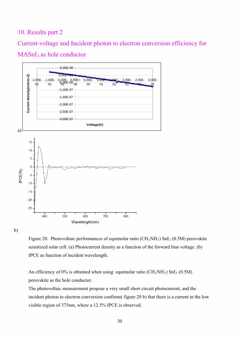
10. Results part 2
Current-voltage and Incident photon to electron conversion efficiency for
MASnI3 as hole conductor
a)
-3,00E-07
-2,50E-07
-2,00E-07
-1,50E-07
-1,00E-07
-5,00E-08
0,00E+00
5,00E-08
-1,50E-01
-1,00E-01
-5,00E-02
0,00E+00
5,00E-02
1,00E-01
1,50E-01
2,00E-01
2,50E-01
3,00E-01
Voltage(V)
Cu
rren
t d
ensi
ty(m
Acm
-2)
b)
Figure 20. Photovoltaic performances of equimolar ratio (CH3NH3) SnI3 (0.5M) perovskite
sensitized solar cell. (a) Photocurrent density as a function of the forward bias voltage. (b)
IPCE as function of incident wavelength.
An efficiency of 0% is obtained when using equimolar ratio (CH3NH3) SnI3 (0.5M)
perovskite as the hole conductor.
The photovoltaic measurement propose a very small short circuit photocurrent, and the
incident photon to electron conversion confirms( figure 20 b) that there is a current in the low
visible region of 375nm, where a 12.5% IPCE is observed.
30

Photo-induced absorption for MASnI3 as hole conductor
Figure 21. Photo-induced absorption spectra of sample containing D35 as light absorbing
material and MASnI3 (0.5M) perovskite as hole conductor.
PIA is used to investigate dye regeneration using (CH3NH3) SnI3 (0.5M) perovskite as a hole
conductor. In figure 21 one can observe a bleaching of the ground state D35 dye at around
570nm. The bleaching occurs as a result of decrease in absorption of the dye. The positive
signal above 610nm is credited to oxidized D35 dye. In the spectra it is seen that the
absorption(positive signal) from the oxidized dye in the interval of 610-730nm has
disappeared when using the perovskite as hole conductor compared to not using it, indicating
dye regeneration(hole transfer to the perovskite). Another observation is that the peak at
around 1200nm has decreased significantly, also probably due to dye regeneration[15].
31

Scanning electron microscopy for MAPbI3 and MASnI3 solar cells
Figure 22. A cross-sectional SEM picture illustrating the different layers in the solar cell with
MAPbI3 as light absorber
In figure 22 one can observe a SEM picture taken with a 40k magnification. Three clear layers
of glass, FTO and underlayer can be seen. Then since the TiO2 is nanoporous it is infiltrate by
the MAPbI3 and spiro-OMeTAD (HTM). And finally on top of the HTM one can narrowly
see the Ag counter electrode.
Figure 23. A cross-sectional SEM picture illustrating the different layers in the solar cell with
MASnI3 as hole conductor
32

In figure 23 one can observe a SEM picture taken with a 40k magnification. Two clear layers
of FTO and underlayer can be seen. Then since the TiO2 is nanoporous it is infiltrate by the
D35 dye and the MASnI3 (HTM).
Figure 24. A cross-sectional SEM picture illustrating the upper layer in the solar cell with
MASnI3 as hole conductor
In figure 24 SEM picture is taken with a 200k magnification. The upper layer is observed
where the TiO2 is infiltrated by the MASnI3 as hole conductor. The TiO2 pores are the darker
regions and is thought to be filled with the MASnI3.
33

11. Conclusions
The MASnI3 perovskite changes colour rapidly when subjected to air(from yellow to
black). Therefore handling this perovskite should be done under air-vacuum, inside
the glovebox.
Equimolar ratio MASnI3 perovskites changes colour when filtrated(from yellow
transparent to yellow non-transparent) leaving the conclusion that a non-filtrated
solution is prefered for solar cell devices. The 3:1 molar ratio MASnI3 is more
stable(doesn't change colour for weeks after filtration).
The UV-vis spectra changes dramatically when adding TiO2 to the samples leaving
the conclusion that TiO2 increases the light absorption of MAPbI3 from 350nm up
around 900 nm. The spectra changes less for MASnI
to
3 when adding TiO2.
The XRD spectra are highly similar except for a few peaks, leading to the conclusion
that MAPbI3 and MASnI3 perovskites have a comparable structure.
Whilst for the MAPbI3 a peak ranging from about 1170-1430nm can be observed
indicating that hole transfer is taking place from the lead perovskite to the spiro-
OMETAD (HTM), there is no hole transfer proved from the MASnI3 perovskite.
When using the equimolar ratio MASnI3 (0.5M) perovskite as the hole conductor an
IPCE of 12.5% was obtained at the low visible region of 375nm. And the photo-
induced absorption measurement concluded that a possible dye regeneration occurs.
MASnI3 perovskite is neither appropriate as light absorbing material nor hole
conducting material in these concentrations evaluated, but more research is needed.
With MAPbI3 as light absorbing material in a solar cell device, it was subjected to
illumination with Air Mass 1.5 sunlight which produced an open circuit voltage Voc of
0.645 V, a short circuit photocurrent Jsc of about 7 mA/cm2, and a fill factor FF of
0.445. This resulted in a power conversion efficiency (PCE) of about 2% and an
incident photon to current efficiency (IPCE) of up to 60%, at the same time showing
great light absorbing spectral performances in the visible and near infrared regions.
34

12. Discussion and Future prospects
Performing the same analyzes again to be able to solidify and verify the results
obtained.
Examine different hole transporting materials such as P3HT, DEH and TPAA to
observe what power conversion efficiencies that can be reached.
New methods are emerging to replace spin coating, such as dip coating.
Make a tin perovskite solar cell device without using TiO2 underlayer. This can help
lowering the conduction band to get a spontaneous electron transfer which is not
thought to currently be the case.
Investigate other molar ratios and concentrations of the tin perovskite.
Vary the temperature for the different annealing/sintering processes, especially
regarding the annealing of the tin perovskite.
Using perovskites as the sensitizer in the solar cells lead to a reduction in interfacial
energy loss compared to DSSCs, but the TiO2 underlayer still needs sintering at
500°C. Al2O3 can solve this problem by being used as a scaffold to replace TiO2. One
can use colloidal chemistry to coat a layer of Al2O3. The main advantage of using
Al2O3 is lowering the annealing temperature from 500°C to a 150°C drying step, thus
lowering the device cost and contributing to possible newer solar cell designs in the
future[17].
Using the MASnI3 perovskite as a hole transporting material rather than a light
absorber. There has been some measurements in this project but more needs to be
done to verify.
Try a 5% flourine doping of the MASnI3 perovskite as this has greatly improved the
efficiency of solar cells using CsSnI3 as hole conductor. Examining the effect of
adding SnF2 and ZnO to the already 5% flourine doped MASnI3 is also interesting
since a efficiency of up to 10.2% has been achieved for the CsSnI3 hole conductor[4].
35

13. Acknowledgments I want to thank my supervisors Byung-wook Park and Erik Johansson for their passion and
great knowledge. You have been really nice and made my thesis a joy. I have learnt a lot
about the basics of solar cell engineering in this short period.
I would also like to thank my reviewer Gerrit Boschloo and everybody else in the physical
chemistry department in Ångström laboratory for making my stay pleasant.
Furthermore I would like to thank my examiner Karin Larsson.
Finally would like to thank my family and friends for always standing up for me!
14. References
1. Nicole Andre Berdelle. Energy agriculture connect, of Prototype creation of the need to accelerating the shift to renewable energy. February 2012.
2. Oliver Morton. Solar energy: A new day dawning?: Silicon Valley sunrise. Published 7 September 2006.
3. Sandra Feldt. Alternative Redox Couples for Dye-Sensitized Solar Cells, chapter 2 and 3. Examined 22 march 2013.
4. In Chung and co-workers. All solid state dye sensitized solar cells with high efficiency. Accepted 8 march 2012.
5. Yasuo Chiba, Ashraful Islam. Dye-Sensitized Solar Cells with Conversion Efficiency of 11.1%,. Published June 23 2006.
6. Akul Mehta. Ultraviolet-Visible (UV-Vis) Spectroscopy – Principle. December 2011. 7. Link: http://www.mpip-mainz.mpg.de/groups/laquai/Research/PIA/?lang=en 8. Link: http://www.mrl.ucsb.edu/mrl/centralfacilities/xray/xray-basics/index.html 9. Link: http://www.mmk.su.se/~lerik/oorganisk_kemi_i_naturen/Rtg.pdf 10. Knoll, Max (1935). "Aufladepotentiel und Sekundäremission elektronenbestrahlter
Körper". Zeitschrift für technische Physik 16: 467–475 11. C.R. Brundle, C.A. Evans, S. Wilson. Encyclopedia of materials characterization,
Butterworth-Heinemann, 1992. 12. Link: http://www.purdue.edu/rem/rs/sem.htm 13. Hui-Seon Kim, Chang-Ryul Lee, Jeong-Hyeok Im. Lead Iodide Perovskite Sensitized
All-Solid-State Submicron Thin Film Mesoscopic Solar Cell with Efficiency Exceeding 9%. Published 21 August 2012.
14. D.B Mitzi . C.A. Field. Transport, optical and magnetic properties of the conducting halide perovskite (CH3NH3)SnI3. Accepted april 25 1994.
15. Byung-wook Park and co-workers. Formation of neutral, polaron and bipolaron states of PEDOT by photo-electrochemical polymerization and the effect of charge generation mechanism in solid state dye sensitized solar cell.
16. Mohammad Hossein Habibi and co-workers. Novel nanostructure zinc zirconate, zinc oxide or zirconium oxide pastes coated on fluorine doped tin oxide thin film as photoelectrochemical working electrodes for dye-sensitized solar cell. Published march 2013.
17. Henry snaith and co-workers. Low-temperature processed meso-superstructured to thin-film perovskite solar cells. Accepted 27 march 2013.
36

37
this project:
15. Appendix
Perovskite optimization for device
Since the first tin based perovskite solution did not work as a solar cell device, two strategies
to optimize the device were followed.
a) The 3:1 molar ratio solution of CH3NH3I: SnI2 did not work in the solar cell device,
which could be due to the fact it was in contact with air. As a result a couple of other
perovskite concentrations and methods were examined. Here one can see all concentrations
examined in
S0-solutions: 3:1 molar ratio solution of CH3NH3I: SnI2. Mix 0.2357g SnI2 +
0.2947g CH3NH3I in 2.5ml of γ-butyrolactone(20wt%) resulting in a 0.25M MASnI3
perovskite solution. Made two samples of this perovskite, one in contact with
air(S0air) and one inside the glovebox(S0gl). The S0air-solution immediately and
completely oxidizes in a matter of seconds when subjected to oxygen.
S1-solution: equimolar ratio of CH3NH3I: SnI2. Mix 0.0935g SnI2+0.035g CH3NH3I
in 0.4ml of anhydrous γ-butyrolactone(20wt%) and 0.1ml N,N-Dimethyl formamide
(DMF) resulting in a 0.5M MASnI3 perovskite solution.
S2-solution: equimolar ratio of CH3NH3I: SnI2. Mix 0.1865g SnI2+0.07g CH3NH3I
in 0.4ml of anhydrous γ-butyrolactone(20wt%)+ 0.1ml DMF resulting in a 1M
MASnI3 perovskite solution.
S3-solution: equimolar ratio of CH3NH3I: SnI2. Mix 0.28g SnI2+0.105g CH3NH3I
in 0.4ml of anhydrous γ-butyrolactone(20wt%)+ 0.1ml DMF resulting in a 1.5M
MASnI3 perovskite solution.
S4-solution: equimolar ratio of CH3NH3I: SnI2. Mix 0.373g SnI2+0.14g CH3NH3I
in 0.4ml of anhydrous γ-butyrolactone(20wt%) and 0.1ml DMF resulting in a 2M
MASnI3 perovskite solution.
S5-solution: equimolar ratio of CH3NH3I: SnI2. Mix 0.0933g SnI2+0.035g CH3NH3I
in 67,5ml DMF resulting in a 4M MASnI3 perovskite solution.
Made also corresponding Lead based perovskites ( L1, L2, L3 and L4) with the same
concentrations to be able to compare the UV-vis and XRD measurement data.