Embed Size (px)
Citation preview
○Product structure:Silicon monolithic integrated circuit ○This product is not designed protection against radioactive rays
.
1/30
TSZ02201-0G1G0AN00010-1-2 © 2013 ROHM Co., Ltd. All rights reserved. TSZ22111・14・001
www.rohm.com
17.FEB.2017 Rev.007
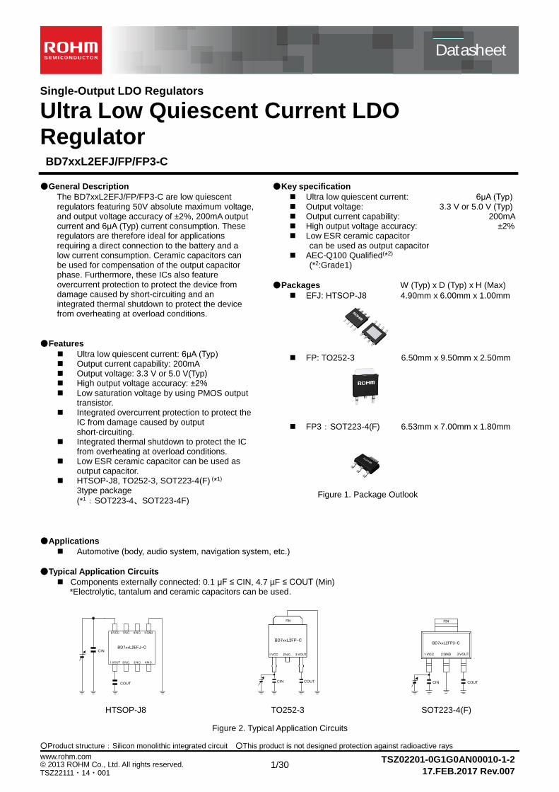
Single-Output LDO Regulators
Ultra Low Quiescent Current LDO Regulator BD7xxL2EFJ/FP/FP3-C
●General Description
The BD7xxL2EFJ/FP/FP3-C are low quiescent regulators featuring 50V absolute maximum voltage, and output voltage accuracy of ±2%, 200mA output current and 6μA (Typ) current consumption. These regulators are therefore ideal for applications requiring a direct connection to the battery and a low current consumption. Ceramic capacitors can be used for compensation of the output capacitor phase. Furthermore, these ICs also feature overcurrent protection to protect the device from damage caused by short-circuiting and an integrated thermal shutdown to protect the device from overheating at overload conditions.
●Features
Ultra low quiescent current: 6μA (Typ) Output current capability: 200mA Output voltage: 3.3 V or 5.0 V(Typ) High output voltage accuracy: ±2% Low saturation voltage by using PMOS output
transistor. Integrated overcurrent protection to protect the
IC from damage caused by output short-circuiting.
Integrated thermal shutdown to protect the IC from overheating at overload conditions.
Low ESR ceramic capacitor can be used as output capacitor.
HTSOP-J8, TO252-3, SOT223-4(F) (*1) 3type package
(*1:SOT223-4、SOT223-4F)
●Key specification
Ultra low quiescent current: 6μA (Typ) Output voltage: 3.3 V or 5.0 V (Typ) Output current capability: 200mA High output voltage accuracy: ±2% Low ESR ceramic capacitor
can be used as output capacitor AEC-Q100 Qualified(*2)
(*2:Grade1)
●Packages W (Typ) x D (Typ) x H (Max)
EFJ: HTSOP-J8 4.90mm x 6.00mm x 1.00mm
FP: TO252-3 6.50mm x 9.50mm x 2.50mm
FP3:SOT223-4(F) 6.53mm x 7.00mm x 1.80mm
●Applications
Automotive (body, audio system, navigation system, etc.)
●Typical Application Circuits
Components externally connected: 0.1 µF ≤ CIN, 4.7 µF ≤ COUT (Min) *Electrolytic, tantalum and ceramic capacitors can be used.
Figure 2. Typical Application Circuits
Figure 1. Package Outlook
HTSOP-J8
FIN
1:VCC 2:GND 3:VOUT
BD7xxL2FP3-CBD7xxL2EFJ-C
8:VCC 7:N.C. 6:N.C. 5:GND
1:VOUT 2:N.C. 3:N.C. 4:N.C.
TO252-3 SOT223-4(F)
1:VCC 2:N.C. 3:VOUT
FIN
BD7xxL2FP-C
CIN
COUT CIN COUT COUT CIN
Datasheet
.
2/30
TSZ02201-0G1G0AN00010-1-2 © 2013 ROHM Co., Ltd. All rights reserved. TSZ22111・15・001
www.rohm.com
BD7xxL2EFJ/FP/FP3-C
17.FEB.2017 Rev.007
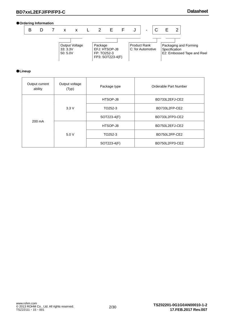
●Ordering Information
B D 7 x x L 2 E F J - C E 2
●Lineup
Output current
ability
Output voltage
(Typ) Package type Orderable Part Number
200 mA
3.3 V
HTSOP-J8 BD733L2EFJ-CE2
TO252-3 BD733L2FP-CE2
SOT223-4(F) BD733L2FP3-CE2
5.0 V
HTSOP-J8 BD750L2EFJ-CE2
TO252-3 BD750L2FP-CE2
SOT223-4(F) BD750L2FP3-CE2
Package EFJ: HTSOP-J8 FP: TO252-3 FP3: SOT223-4(F)
Packaging and Forming Specification E2: Embossed Tape and Reel
Output Voltage 33: 3.3V 50: 5.0V
Product Rank C: for Automotive
.
3/30
TSZ02201-0G1G0AN00010-1-2 © 2013 ROHM Co., Ltd. All rights reserved. TSZ22111・15・001
www.rohm.com
BD7xxL2EFJ/FP/FP3-C
17.FEB.2017 Rev.007
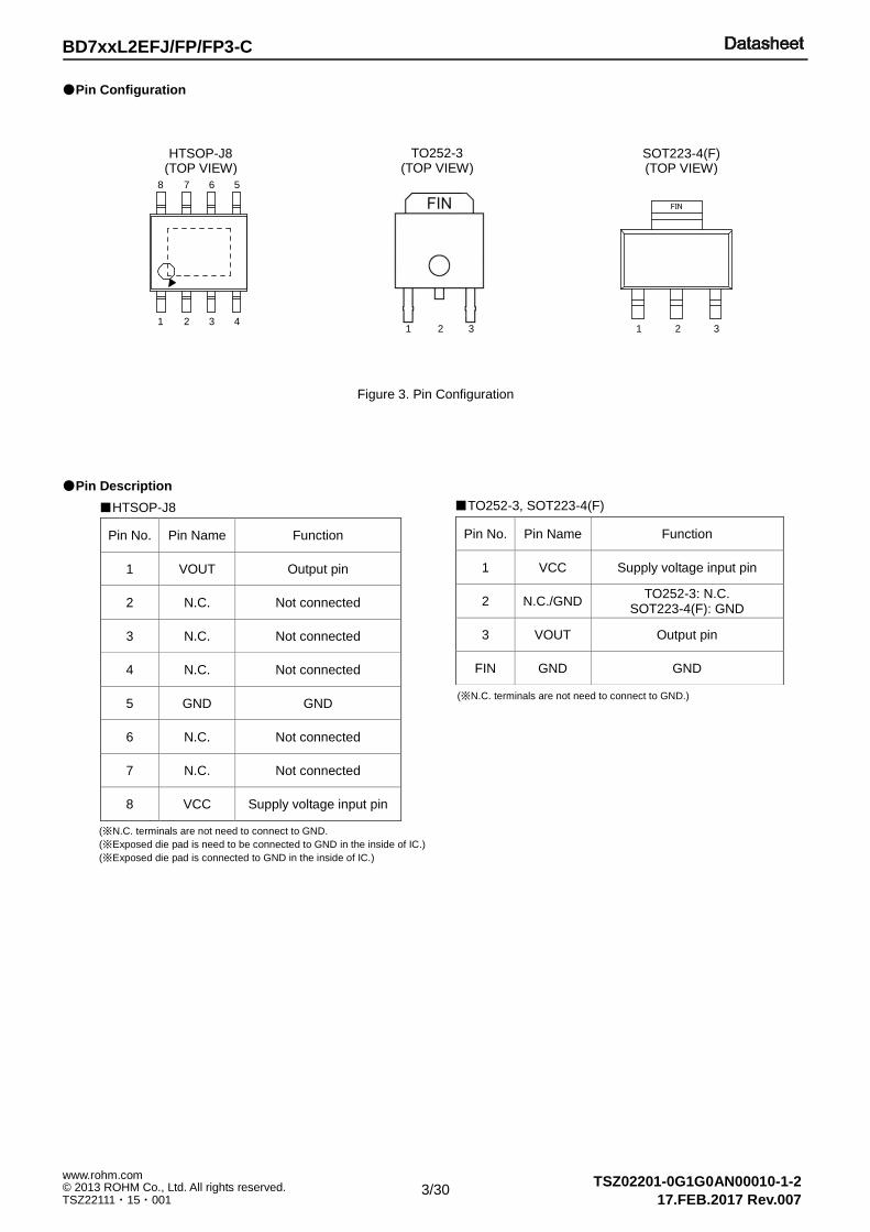
●Pin Configuration
Figure 3. Pin Configuration
●Pin Description
Pin No. Pin Name Function
1 VOUT Output pin
2 N.C. Not connected
3 N.C. Not connected
4 N.C. Not connected
5 GND GND
6 N.C. Not connected
7 N.C. Not connected
8 VCC Supply voltage input pin
Pin No. Pin Name Function
1 VCC Supply voltage input pin
2 N.C./GND TO252-3: N.C.
SOT223-4(F): GND
3 VOUT Output pin
FIN GND GND
■HTSOP-J8
(※N.C. terminals are not need to connect to GND.
(※Exposed die pad is need to be connected to GND in the inside of IC.)
(※Exposed die pad is connected to GND in the inside of IC.)
(※N.C. terminals are not need to connect to GND.)
■TO252-3, SOT223-4(F)
HTSOP-J8 (TOP VIEW)
TO252-3 (TOP VIEW)
SOT223-4(F) (TOP VIEW)
1 2 3 4
8 7 6 5
1 2 3
FIN
1 2 3
.
4/30
TSZ02201-0G1G0AN00010-1-2 © 2013 ROHM Co., Ltd. All rights reserved. TSZ22111・15・001
www.rohm.com
BD7xxL2EFJ/FP/FP3-C
17.FEB.2017 Rev.007
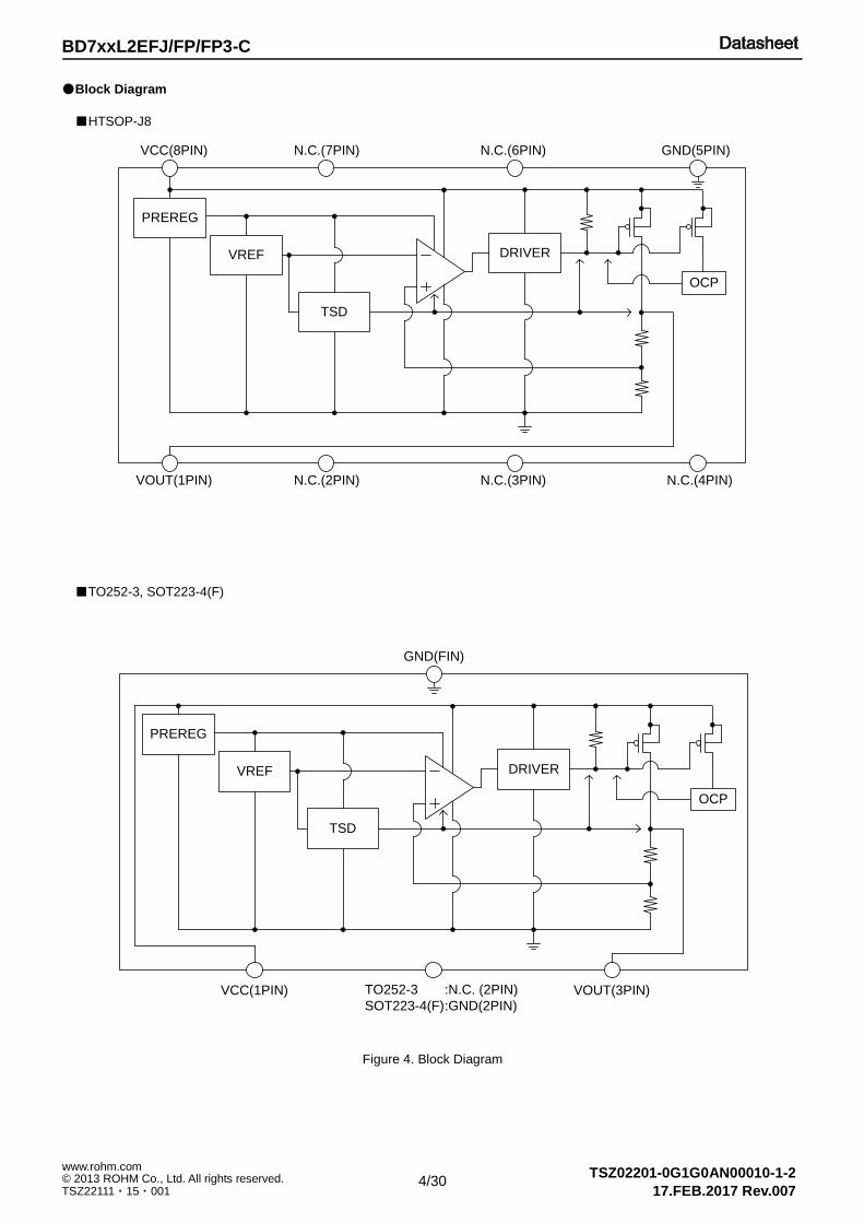
●Block Diagram
■HTSOP-J8
■TO252-3, SOT223-4(F)
Figure 4. Block Diagram
PREREG
VREF DRIVER
OCP
VCC(8PIN) N.C.(7PIN) N.C.(6PIN) GND(5PIN)
VOUT(1PIN) N.C.(2PIN) N.C.(3PIN) N.C.(4PIN)
TSD
PREREG
VREF DRIVER
OCP
GND(FIN)
VCC(1PIN) VOUT(3PIN)
TSD
TO252-3
SOT223-4(F)
:N.C. (2PIN)
:GND(2PIN)
.
5/30
TSZ02201-0G1G0AN00010-1-2 © 2013 ROHM Co., Ltd. All rights reserved. TSZ22111・15・001
www.rohm.com
BD7xxL2EFJ/FP/FP3-C
17.FEB.2017 Rev.007
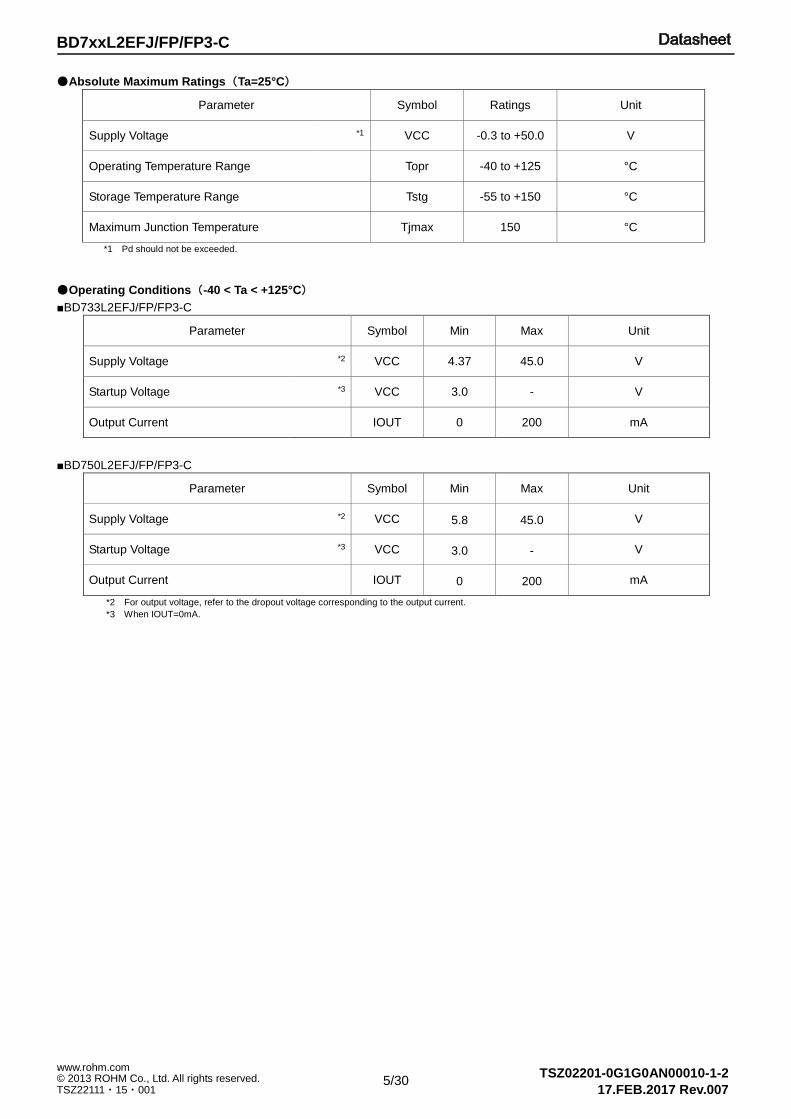
●Absolute Maximum Ratings(Ta=25°C)
Parameter Symbol Ratings Unit
Supply Voltage *1 VCC -0.3 to +50.0 V
Operating Temperature Range Topr -40 to +125 °C
Storage Temperature Range Tstg -55 to +150 °C
Maximum Junction Temperature Tjmax 150 °C
*1 Pd should not be exceeded.
●Operating Conditions(-40 < Ta < +125°C)
■BD733L2EFJ/FP/FP3-C
Parameter Symbol Min Max Unit
Supply Voltage *2 VCC 4.37 45.0 V
Startup Voltage *3 VCC 3.0 - V
Output Current IOUT 0 200 mA
■BD750L2EFJ/FP/FP3-C
Parameter Symbol Min Max Unit
Supply Voltage *2 VCC 5.8 45.0 V
Startup Voltage *3 VCC 3.0 - V
Output Current IOUT 0 200 mA
*2 For output voltage, refer to the dropout voltage corresponding to the output current.
*3 When IOUT=0mA.
.
6/30
TSZ02201-0G1G0AN00010-1-2 © 2013 ROHM Co., Ltd. All rights reserved. TSZ22111・15・001
www.rohm.com
BD7xxL2EFJ/FP/FP3-C
17.FEB.2017 Rev.007
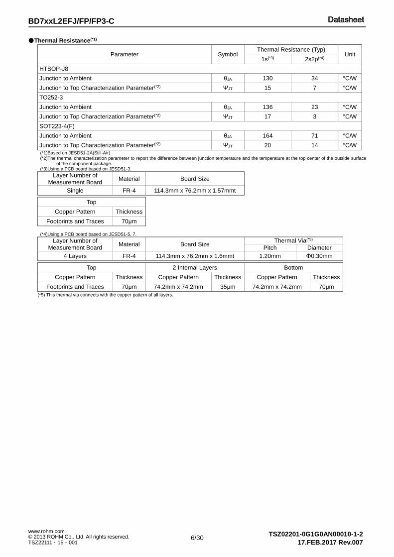
●Thermal Resistance(*1)
Parameter Symbol Thermal Resistance (Typ)
Unit 1s(*3) 2s2p(*4)
HTSOP-J8
Junction to Ambient θJA 130 34 °C/W
Junction to Top Characterization Parameter(*2) ΨJT 15 7 °C/W
TO252-3
Junction to Ambient θJA 136 23 °C/W
Junction to Top Characterization Parameter(*2) ΨJT 17 3 °C/W
SOT223-4(F)
Junction to Ambient θJA 164 71 °C/W
Junction to Top Characterization Parameter(*2) ΨJT 20 14 °C/W
(*1)Based on JESD51-2A(Still-Air). (*2)The thermal characterization parameter to report the difference between junction temperature and the temperature at the top center of the outside surface
of the component package. (*3)Using a PCB board based on JESD51-3.
Layer Number of Measurement Board
Material Board Size
Single FR-4 114.3mm x 76.2mm x 1.57mmt
Top
Copper Pattern Thickness
Footprints and Traces 70μm
(*4)Using a PCB board based on JESD51-5, 7.
Layer Number of Measurement Board
Material Board Size Thermal Via(*5)
Pitch Diameter
4 Layers FR-4 114.3mm x 76.2mm x 1.6mmt 1.20mm Φ0.30mm
Top 2 Internal Layers Bottom
Copper Pattern Thickness Copper Pattern Thickness Copper Pattern Thickness
Footprints and Traces 70μm 74.2mm x 74.2mm 35μm 74.2mm x 74.2mm 70μm
(*5) This thermal via connects with the copper pattern of all layers.
.
7/30
TSZ02201-0G1G0AN00010-1-2 © 2013 ROHM Co., Ltd. All rights reserved. TSZ22111・15・001
www.rohm.com
BD7xxL2EFJ/FP/FP3-C
17.FEB.2017 Rev.007
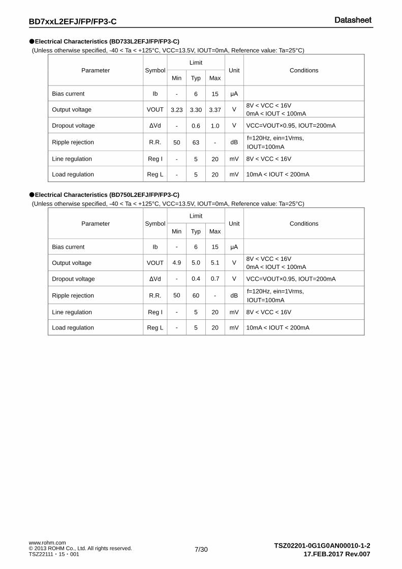
●Electrical Characteristics (BD733L2EFJ/FP/FP3-C)
(Unless otherwise specified, -40 < Ta < +125°C, VCC=13.5V, IOUT=0mA, Reference value: Ta=25°C)
Parameter Symbol
Limit
Unit Conditions
Min Typ Max
Bias current Ib - 6 15 μA
Output voltage VOUT 3.23 3.30 3.37 V 8V < VCC < 16V
0mA < IOUT < 100mA
Dropout voltage ΔVd - 0.6 1.0 V VCC=VOUT×0.95, IOUT=200mA
Ripple rejection R.R. 50 63 - dB f=120Hz, ein=1Vrms,
IOUT=100mA
Line regulation Reg I - 5 20 mV 8V < VCC < 16V
Load regulation Reg L - 5 20 mV 10mA < IOUT < 200mA
●Electrical Characteristics (BD750L2EFJ/FP/FP3-C)
(Unless otherwise specified, -40 < Ta < +125°C, VCC=13.5V, IOUT=0mA, Reference value: Ta=25°C)
Parameter Symbol
Limit
Unit Conditions
Min Typ Max
Bias current Ib - 6 15 μA
Output voltage VOUT 4.9 5.0 5.1 V 8V < VCC < 16V
0mA < IOUT < 100mA
Dropout voltage ΔVd - 0.4 0.7 V VCC=VOUT×0.95, IOUT=200mA
Ripple rejection R.R. 50 60 - dB f=120Hz, ein=1Vrms,
IOUT=100mA
Line regulation Reg I - 5 20 mV 8V < VCC < 16V
Load regulation Reg L - 5 20 mV 10mA < IOUT < 200mA
.
8/30
TSZ02201-0G1G0AN00010-1-2 © 2013 ROHM Co., Ltd. All rights reserved. TSZ22111・15・001
www.rohm.com
BD7xxL2EFJ/FP/FP3-C
17.FEB.2017 Rev.007
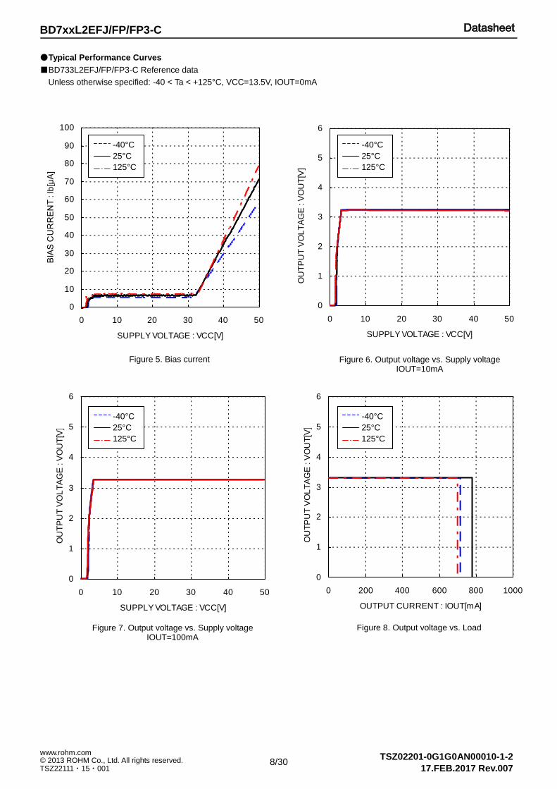
●Typical Performance Curves
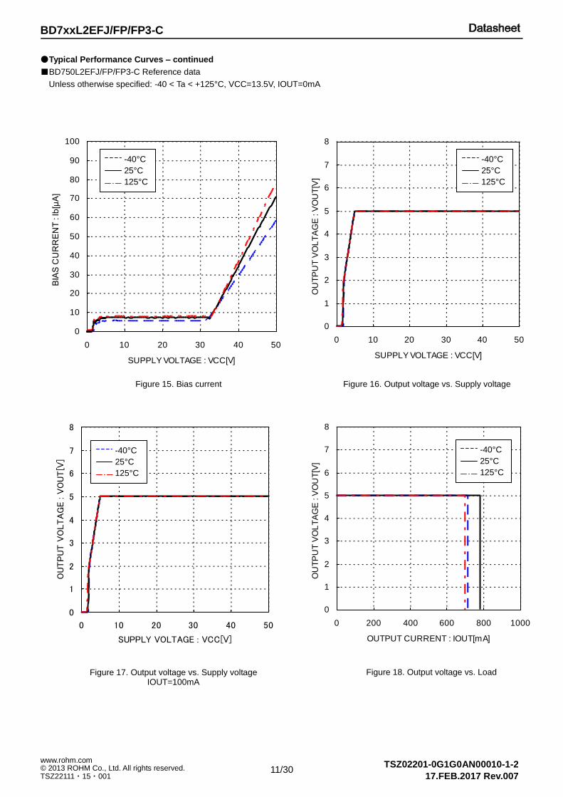
■BD733L2EFJ/FP/FP3-C Reference data
Unless otherwise specified: -40 < Ta < +125°C, VCC=13.5V, IOUT=0mA
0
1
2
3
4
5
6
0 10 20 30 40 50
SUPPLY VOLTAGE : VCC[V]
OU
TP
UT
VO
LT
AG
E : V
OU
T[V
]
Figure 5. Bias current
Figure 8. Output voltage vs. Load
Figure 6. Output voltage vs. Supply voltage IOUT=10mA
Figure 7. Output voltage vs. Supply voltage IOUT=100mA
0
1
2
3
4
5
6
0 10 20 30 40 50
SUPPLY VOLTAGE : VCC[V]
OU
TP
UT
VO
LT
AG
E : V
OU
T[V
]
0
1
2
3
4
5
6
0 200 400 600 800 1000
OUTPUT CURRENT : IOUT[mA]
OU
TP
UT
VO
LT
AG
E : V
OU
T[V
]
-40°C
25°C
125°C
-40°C
25°C
125°C
-40°C
25°C
125°C
0
10
20
30
40
50
60
70
80
90
100
0 10 20 30 40 50
SUPPLY VOLTAGE : VCC[V]
BIA
S C
URRENT : lb[μ
A]
-40°C
25°C
125°C
.
9/30
TSZ02201-0G1G0AN00010-1-2 © 2013 ROHM Co., Ltd. All rights reserved. TSZ22111・15・001
www.rohm.com
BD7xxL2EFJ/FP/FP3-C
17.FEB.2017 Rev.007
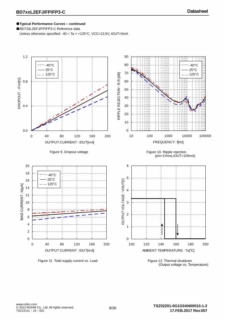
●Typical Performance Curves – continued
■BD733L2EFJ/FP/FP3-C Reference data
Unless otherwise specified: -40 < Ta < +125°C, VCC=13.5V, IOUT=0mA
0
1
2
3
4
5
6
100 120 140 160 180 200
AMBIENT TEMPERATURE : Ta[℃]
OU
TP
UT
VO
LT
AG
E : V
OU
T[V
]
Figure 9. Dropout voltage Figure 10. Ripple rejection (ein=1Vrms,IOUT=100mA)
0.0
0.4
0.8
1.2
0 40 80 120 160 200
OUTPUT CURRENT : IOUT[mA]
DR
OP
OU
T : △
Vd
[V]
0
10
20
30
40
50
60
70
80
90
10 100 1000 10000 100000
FREQUENCY : f[Hz]
RIP
PL
E R
EJE
CT
ION
: R
.R.[d
B]
-40°C
25°C
125°C
-40°C
25°C
125°C
0
2
4
6
8
10
12
14
16
18
20
0 40 80 120 160 200
OUTPUT CURRENT : IOUT[mA]
BIA
S C
URRENT : lb[μ
A]
-40°C
25°C
125°C
Figure 11. Total supply current vs. Load Figure 12. Thermal shutdown (Output voltage vs. Temperature)
.
10/30
TSZ02201-0G1G0AN00010-1-2 © 2013 ROHM Co., Ltd. All rights reserved. TSZ22111・15・001
www.rohm.com
BD7xxL2EFJ/FP/FP3-C
17.FEB.2017 Rev.007
●Typical Performance Curves – continued
■BD733L2EFJ/FP/FP3-C Reference data
Unless otherwise specified: -40 < Ta < +125°C, VCC=13.5V, IOUT=0mA
4
5
6
7
8
9
10
-40 0 40 80 120
AMBIENT TEMPERATURE : Ta[℃]
BIA
S C
URRENT : lb[μ
A]
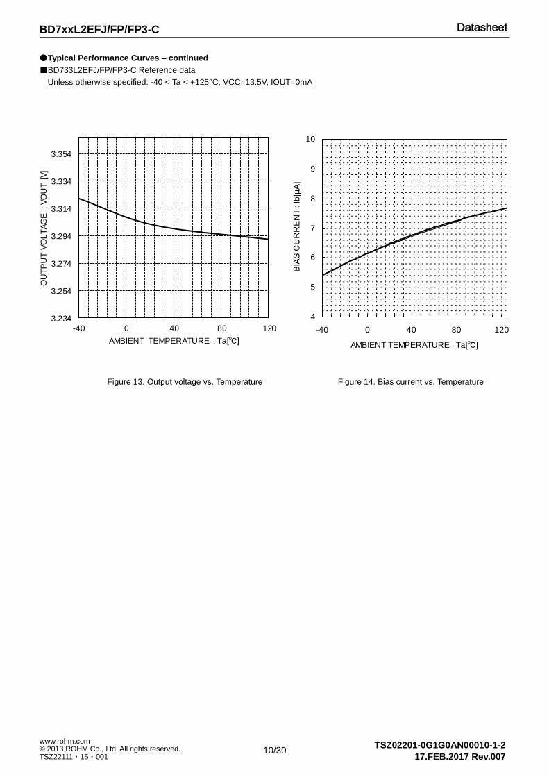
3.234
3.254
3.274
3.294
3.314
3.334
3.354
-40 0 40 80 120
OU
TP
UT
VO
LT
AG
E : V
OU
T [
V]
AMBIENT TEMPERATURE : Ta[℃]
Figure 13. Output voltage vs. Temperature Figure 14. Bias current vs. Temperature
.
11/30
TSZ02201-0G1G0AN00010-1-2 © 2013 ROHM Co., Ltd. All rights reserved. TSZ22111・15・001
www.rohm.com
BD7xxL2EFJ/FP/FP3-C
17.FEB.2017 Rev.007
●Typical Performance Curves – continued
■BD750L2EFJ/FP/FP3-C Reference data
Unless otherwise specified: -40 < Ta < +125°C, VCC=13.5V, IOUT=0mA
0
1
2
3
4
5
6
7
8
0 200 400 600 800 1000
OUTPUT CURRENT : IOUT[mA]
OU
TP
UT
VO
LT
AG
E : V
OU
T[V
] .
0
1
2
3
4
5
6
7
8
0 10 20 30 40 50
SUPPLY VOLTAGE : VCC[V]
OU
TP
UT
VO
LT
AG
E : V
OU
T[V
] .
Figure 18. Output voltage vs. Load
-40°C
25°C
125°C
-40°C
25°C
125°C
0
10
20
30
40
50
60
70
80
90
100
0 10 20 30 40 50
SUPPLY VOLTAGE : VCC[V]
BIA
S C
URRENT : lb[μ
A] .
-40°C
25°C
125°C
0
1
2
3
4
5
6
7
8
0 10 20 30 40 50
SUPPLY VOLTAGE : VCC[V]
OU
TP
UT
VO
LT
AG
E : V
OU
T[V
]
-40°C
25°C
125°C
Figure 15. Bias current Figure 16. Output voltage vs. Supply voltage
Figure 17. Output voltage vs. Supply voltage IOUT=100mA
.
12/30
TSZ02201-0G1G0AN00010-1-2 © 2013 ROHM Co., Ltd. All rights reserved. TSZ22111・15・001
www.rohm.com
BD7xxL2EFJ/FP/FP3-C
17.FEB.2017 Rev.007
●Typical Performance Curves – continued
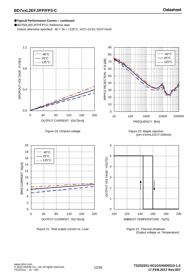
■BD750L2EFJ/FP/FP3-C Reference data
Unless otherwise specified: -40 < Ta < +125°C, VCC=13.5V, IOUT=0mA
0
10
20
30
40
50
60
70
80
90
10 100 1000 10000 100000
FREQUENCY : f[Hz]
RIP
PL
E R
EJE
CT
ION
: R
.R.[d
B]
0
1
2
3
4
5
6
100 120 140 160 180 200
AMBIENT TEMPERATURE : Ta[℃]
OU
TP
UT
VO
LT
AG
E : V
OU
T[V
]
Figure 20. Ripple rejection (ein=1Vrms,IOUT=100mA)
Figure 21. Total supply current vs. Load
Figure 19. Dropout voltage
-40°C
25°C
125°C
0
2
4
6
8
10
12
14
16
18
20
0 40 80 120 160 200
OUTPUT CURRENT : IOUT[mA]
BIA
S C
URRENT : lb[μ
A] .
-40°C
25°C
125°C
0.0
0.4
0.8
1.2
0 40 80 120 160 200
OUTPUT CURRENT : IOUT[mA]
DR
OP
OU
T V
OL
TA
GE
: △
Vd
[V]
-40°C
25°C
125°C
Figure 22. Thermal shutdown (Output voltage vs. Temperature)
.
13/30
TSZ02201-0G1G0AN00010-1-2 © 2013 ROHM Co., Ltd. All rights reserved. TSZ22111・15・001
www.rohm.com
BD7xxL2EFJ/FP/FP3-C
17.FEB.2017 Rev.007
●Typical Performance Curves – continued
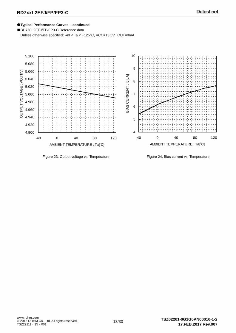
■BD750L2EFJ/FP/FP3-C Reference data
Unless otherwise specified: -40 < Ta < +125°C, VCC=13.5V, IOUT=0mA
Figure 23. Output voltage vs. Temperature
Figure 24. Bias current vs. Temperature
4.900
4.920
4.940
4.960
4.980
5.000
5.020
5.040
5.060
5.080
5.100
-40 0 40 80 120
AMBIENT TEMPERATURE : Ta[℃]
OU
TP
UT
VO
LT
AG
E : V
OU
T[V
]
4
5
6
7
8
9
10
-40 0 40 80 120
AMBIENT TEMPERATURE : Ta[℃]
BIA
S C
URRENT : lb[μ
A]
.
14/30
TSZ02201-0G1G0AN00010-1-2 © 2013 ROHM Co., Ltd. All rights reserved. TSZ22111・15・001
www.rohm.com
BD7xxL2EFJ/FP/FP3-C
17.FEB.2017 Rev.007
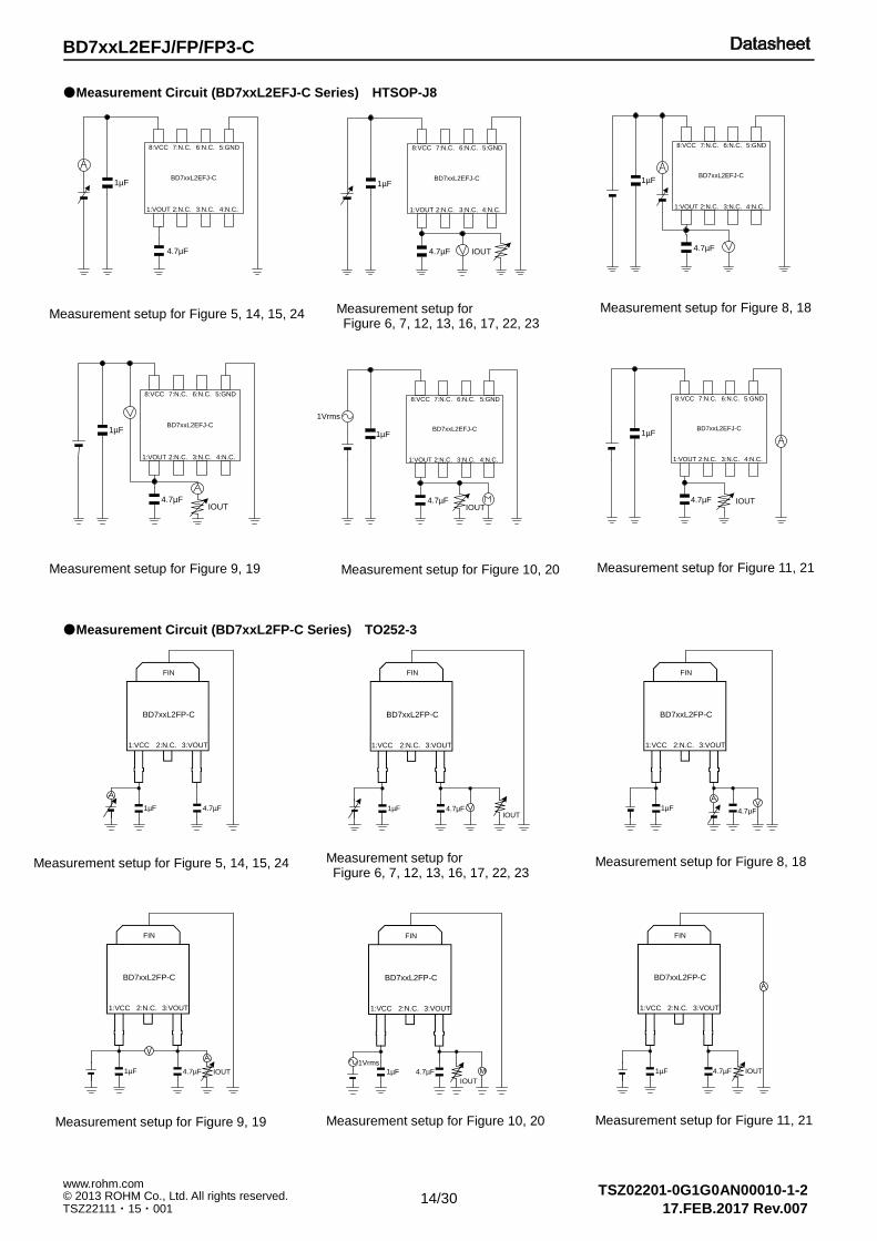
●Measurement Circuit (BD7xxL2EFJ-C Series) HTSOP-J8
●Measurement Circuit (BD7xxL2FP-C Series) TO252-3
Measurement setup for Figure 5, 14, 15, 24 Measurement setup for Figure 6, 7, 12, 13, 16, 17, 22, 23
Measurement setup for Figure 8, 18
Measurement setup for Figure 9, 19 Measurement setup for Figure 10, 20 Measurement setup for Figure 11, 21
Measurement setup for Figure 5, 14, 15, 24 Measurement setup for Figure 6, 7, 12, 13, 16, 17, 22, 23
Measurement setup for Figure 8, 18
Measurement setup for Figure 9, 19 Measurement setup for Figure 10, 20 Measurement setup for Figure 11, 21
BD7xxL2EFJ-C
8:VCC 7:N.C. 6:N.C. 5:GND
1:VOUT 2:N.C. 3:N.C. 4:N.C.
1µF
4.7µF
1Vrms
IOUT
BD7xxL2EFJ-C
8:VCC 7:N.C. 6:N.C. 5:GND
1:VOUT 2:N.C. 3:N.C. 4:N.C.
1µF
4.7µF IOUT
BD7xxL2EFJ-C
8:VCC 7:N.C. 6:N.C. 5:GND
1:VOUT 2:N.C. 3:N.C. 4:N.C.
1µF
4.7µFIOUT
BD7xxL2EFJ-C
8:VCC 7:N.C. 6:N.C. 5:GND
1:VOUT 2:N.C. 3:N.C. 4:N.C.
1µF
4.7µF
BD7xxL2EFJ-C
8:VCC 7:N.C. 6:N.C. 5:GND
1:VOUT 2:N.C. 3:N.C. 4:N.C.
1µF
4.7µF
BD7xxL2EFJ-C
8:VCC 7:N.C. 6:N.C. 5:GND
1:VOUT 2:N.C. 3:N.C. 4:N.C.
1µF
4.7µF IOUT
1:VCC 2:N.C. 3:VOUT
FIN
BD7xxL2FP-C
4.7µF1µF
1:VCC 2:N.C. 3:VOUT
FIN
BD7xxL2FP-C
4.7µF1µFIOUT
1:VCC 2:N.C. 3:VOUT
FIN
BD7xxL2FP-C
4.7µF1µF
1:VCC 2:N.C. 3:VOUT
FIN
BD7xxL2FP-C
4.7µF1µF IOUT
1:VCC 2:N.C. 3:VOUT
FIN
BD7xxL2FP-C
4.7µF1µF
IOUT
1VrmsM
1:VCC 2:N.C. 3:VOUT
FIN
BD7xxL2FP-C
4.7µF1µF IOUT
.
15/30
TSZ02201-0G1G0AN00010-1-2 © 2013 ROHM Co., Ltd. All rights reserved. TSZ22111・15・001
www.rohm.com
BD7xxL2EFJ/FP/FP3-C
17.FEB.2017 Rev.007
●Measurement Circuit (BD7xxL2FP3-C Series) SOT223-4(F)
4.7uF
1uFIOUT
FIN
1:VCC 2:GND 3:VOUT
BD7xxL2FP3-C
4.7uF
1uFIOUT
FIN
1:VCC 2:GND 3:VOUT
BD7xxL2FP3-C
4.7uF1uF
FIN
1:VCC 2:GND 3:VOUT
BD7xxL2FP3-C
4.7uF1uF
FIN
1:VCC 2:GND 3:VOUT
BD7xxL2FP3-C
4.7uF1uF
FIN
1:VCC 2:GND 3:VOUT
BD7xxL2FP3-C
Measurement setup for Figure 5, 14, 15, 24 Measurement setup for Figure 6, 7, 12, 13, 16, 17, 22, 23
Measurement setup for Figure 8, 18
Measurement setup for Figure 9, 19 Measurement setup for Figure 10, 20 Measurement setup for Figure 11, 21
1uF
1Vrms
4.7uFM
IOUT
FIN
1:VCC 2:GND 3:VOUT
BD7xxL2FP3-C
.
16/30
TSZ02201-0G1G0AN00010-1-2 © 2013 ROHM Co., Ltd. All rights reserved. TSZ22111・15・001
www.rohm.com
BD7xxL2EFJ/FP/FP3-C
17.FEB.2017 Rev.007
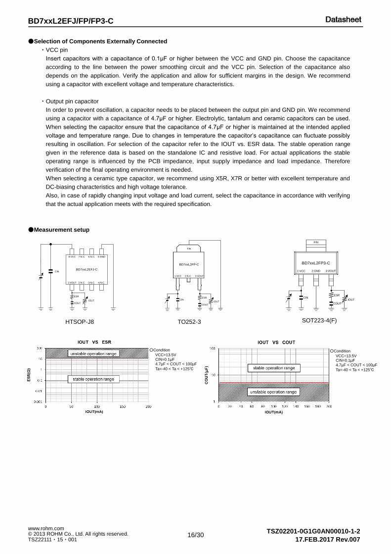
●Selection of Components Externally Connected
・VCC pin
Insert capacitors with a capacitance of 0.1μF or higher between the VCC and GND pin. Choose the capacitance
according to the line between the power smoothing circuit and the VCC pin. Selection of the capacitance also
depends on the application. Verify the application and allow for sufficient margins in the design. We recommend
using a capacitor with excellent voltage and temperature characteristics.
・Output pin capacitor
In order to prevent oscillation, a capacitor needs to be placed between the output pin and GND pin. We recommend
using a capacitor with a capacitance of 4.7μF or higher. Electrolytic, tantalum and ceramic capacitors can be used.
When selecting the capacitor ensure that the capacitance of 4.7μF or higher is maintained at the intended applied
voltage and temperature range. Due to changes in temperature the capacitor’s capacitance can fluctuate possibly
resulting in oscillation. For selection of the capacitor refer to the IOUT vs. ESR data. The stable operation range
given in the reference data is based on the standalone IC and resistive load. For actual applications the stable
operating range is influenced by the PCB impedance, input supply impedance and load impedance. Therefore
verification of the final operating environment is needed.
When selecting a ceramic type capacitor, we recommend using X5R, X7R or better with excellent temperature and
DC-biasing characteristics and high voltage tolerance.
Also, in case of rapidly changing input voltage and load current, select the capacitance in accordance with verifying
that the actual application meets with the required specification.
●Measurement setup
○Condition
VCC=13.5V CIN=0.1μF 4.7µF < COUT < 100µF
Ta=-40 < Ta < +125℃
○Condition
VCC=13.5V CIN=0.1µF 4.7µF < COUT < 100µF
Ta=-40 < Ta < +125℃
TO252-3 SOT223-4(F) HTSOP-J8
1:VCC 2:N.C. 3:VOUT
FIN
BD7xxL2FP-C
CINESR
COUT
IOUT
CINESR
COUT
IOUT
FIN
1:VCC 2:GND 3:VOUT
BD7xxL2FP3-C
BD7xxL2EFJ-C
8:VCC 7:N.C. 6:N.C. 5:GND
1:VOUT 2:N.C. 3:N.C. 4:N.C.
CIN
IOUTCOUT
ESR
.
17/30
TSZ02201-0G1G0AN00010-1-2 © 2013 ROHM Co., Ltd. All rights reserved. TSZ22111・15・001
www.rohm.com
BD7xxL2EFJ/FP/FP3-C
17.FEB.2017 Rev.007
①0.96 W
②3.67 W
0.0
1.0
2.0
3.0
4.0
5.0
0 25 50 75 100 125 150
Po
we
r D
issip
atio
n: P
d[W
]
Ambient Temperature: Ta [ C]
①0.92 W
②5.43 W
0.0
2.0
4.0
6.0
8.0
10.0
0 25 50 75 100 125 150
Po
we
r D
issip
atio
n: P
d[W
]
Ambient Temperature: Ta [ C]
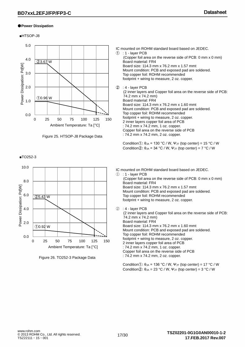
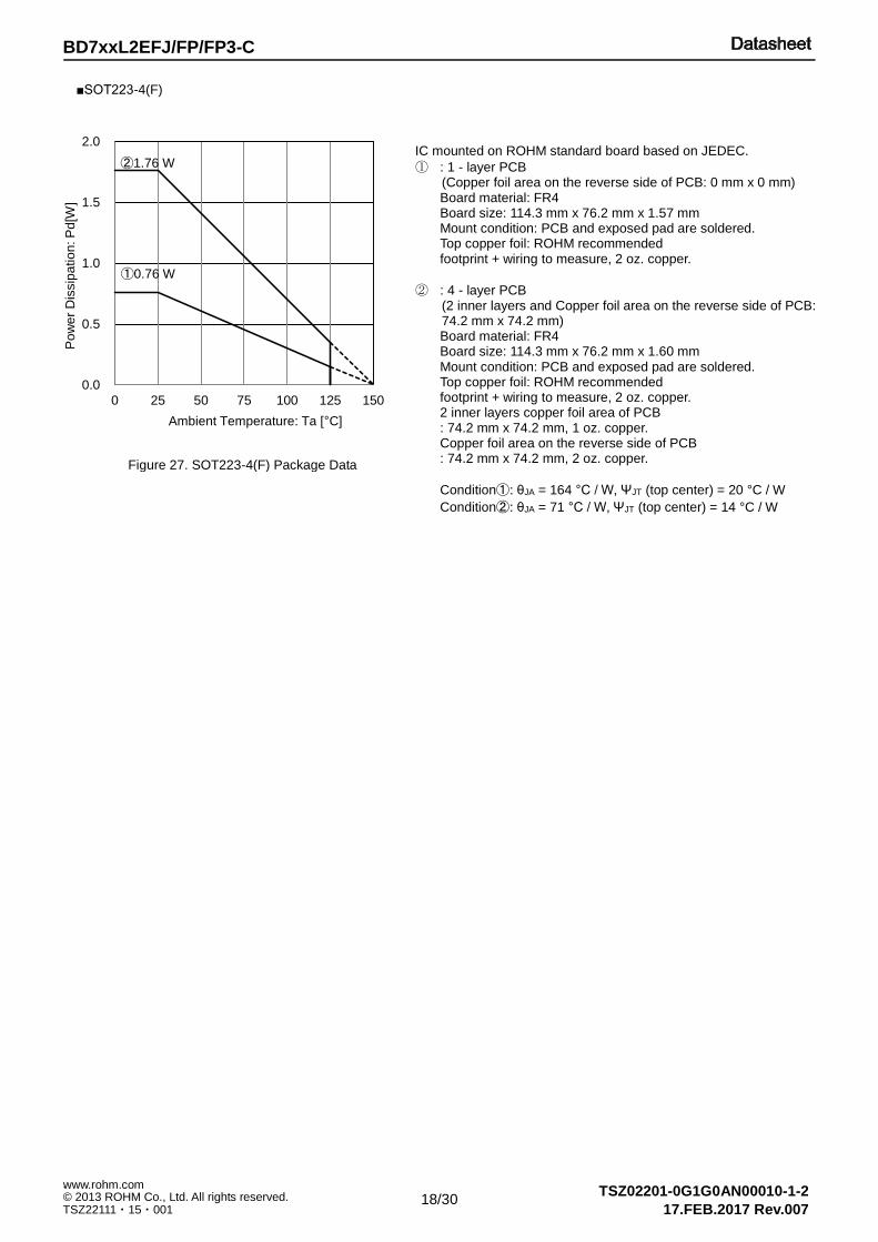
●Power Dissipation
■HTSOP-J8
IC mounted on ROHM standard board based on JEDEC.
① : 1 - layer PCB (Copper foil area on the reverse side of PCB: 0 mm x 0 mm) Board material: FR4 Board size: 114.3 mm x 76.2 mm x 1.57 mmt Mount condition: PCB and exposed pad are soldered. Top copper foil: ROHM recommended footprint + wiring to measure, 2 oz. copper.
② : 4 - layer PCB (2 inner layers and Copper foil area on the reverse side of PCB: 74.2 mm x 74.2 mm) Board material: FR4 Board size: 114.3 mm x 76.2 mm x 1.60 mmt Mount condition: PCB and exposed pad are soldered. Top copper foil: ROHM recommended footprint + wiring to measure, 2 oz. copper. 2 inner layers copper foil area of PCB : 74.2 mm x 74.2 mm, 1 oz. copper. Copper foil area on the reverse side of PCB : 74.2 mm x 74.2 mm, 2 oz. copper.
Condition①: θJA = 130 C / W, ΨJT (top center) = 15 °C / W
Condition②: θJA = 34 C / W, ΨJT (top center) = 7 °C / W
■TO252-3
IC mounted on ROHM standard board based on JEDEC.
① : 1 - layer PCB (Copper foil area on the reverse side of PCB: 0 mm x 0 mm) Board material: FR4 Board size: 114.3 mm x 76.2 mm x 1.57 mmt Mount condition: PCB and exposed pad are soldered. Top copper foil: ROHM recommended footprint + wiring to measure, 2 oz. copper.
② : 4 - layer PCB (2 inner layers and Copper foil area on the reverse side of PCB: 74.2 mm x 74.2 mm) Board material: FR4 Board size: 114.3 mm x 76.2 mm x 1.60 mmt Mount condition: PCB and exposed pad are soldered. Top copper foil: ROHM recommended footprint + wiring to measure, 2 oz. copper. 2 inner layers copper foil area of PCB : 74.2 mm x 74.2 mm, 1 oz. copper. Copper foil area on the reverse side of PCB : 74.2 mm x 74.2 mm, 2 oz. copper.
Condition①: θJA = 136 C / W, ΨJT (top center) = 17 °C / W
Condition②: θJA = 23 °C / W, ΨJT (top center) = 3 °C / W
Figure 25. HTSOP-J8 Package Data
Figure 26. TO252-3 Package Data
.
18/30
TSZ02201-0G1G0AN00010-1-2 © 2013 ROHM Co., Ltd. All rights reserved. TSZ22111・15・001
www.rohm.com
BD7xxL2EFJ/FP/FP3-C
17.FEB.2017 Rev.007
■SOT223-4(F)
IC mounted on ROHM standard board based on JEDEC.
① : 1 - layer PCB (Copper foil area on the reverse side of PCB: 0 mm x 0 mm) Board material: FR4 Board size: 114.3 mm x 76.2 mm x 1.57 mm Mount condition: PCB and exposed pad are soldered. Top copper foil: ROHM recommended footprint + wiring to measure, 2 oz. copper.
② : 4 - layer PCB (2 inner layers and Copper foil area on the reverse side of PCB: 74.2 mm x 74.2 mm) Board material: FR4 Board size: 114.3 mm x 76.2 mm x 1.60 mm Mount condition: PCB and exposed pad are soldered. Top copper foil: ROHM recommended footprint + wiring to measure, 2 oz. copper. 2 inner layers copper foil area of PCB : 74.2 mm x 74.2 mm, 1 oz. copper. Copper foil area on the reverse side of PCB : 74.2 mm x 74.2 mm, 2 oz. copper.
Condition①: θJA = 164 C / W, ΨJT (top center) = 20 °C / W
Condition②: θJA = 71 C / W, ΨJT (top center) = 14 °C / W
Figure 27. SOT223-4(F) Package Data
①0.76 W
②1.76 W
0.0
0.5
1.0
1.5
2.0
0 25 50 75 100 125 150
Po
we
r D
issip
atio
n: P
d[W
]
Ambient Temperature: Ta [ C]
.
19/30
TSZ02201-0G1G0AN00010-1-2 © 2013 ROHM Co., Ltd. All rights reserved. TSZ22111・15・001
www.rohm.com
BD7xxL2EFJ/FP/FP3-C
17.FEB.2017 Rev.007
Refer to the heat mitigation characteristics illustrated in Figure 25 to Figure 27 when using the IC in an environment of Ta≥25°C. The characteristics of the IC are greatly influenced by the operating temperature, and it is necessary to operate under the maximum junction temperature Timax. Even if the ambient temperature Ta is at 25°C it is possible that the junction temperature Tj reaches high temperatures. Therefore, the IC should be operated within the power dissipation range.
The following method is used to calculate the power consumption Pc (W)
Pc=(VCC-VOUT)×IOUT+VCC×Ib
Power dissipation Pd ≥ Pc The load current Lo is obtained by operating the IC within the power dissipation range.
(Refer to Figure 11 and Figure 21 for the Ib) Thus, the maximum load current IOUTmax for the applied voltage VCC can be calculated during the thermal design process.
●HTSOP-J8
■Calculation example 1) with Ta=125°C, VCC=13.5V, VOUT=3.3V
At Ta=125°C with Figure 25 ② condition, the calculation shows that ca 71.5mA of output current is possible at 10.2V potential
difference across input and output.
■Calculation example 2) with Ta=125°C, VCC=13.5V, VOUT=5.0V
At Ta=125°C with Figure 25 ② condition, the calculation shows that ca 85.8mA of output current is possible at 8.5V potential
difference across input and output. The thermal calculation shown above should be taken into consideration during the thermal design in order to keep the whole operating temperature range within the power dissipation range. In the event of shorting (i.e. VOUT and GND pins are shorted) the power consumption Pc of the IC can be calculated as follows:
Pc=VCC×(Ib+Ishort) (Refer to Figure 8 and Figure 18 for the Ishort)
VCC : Input voltage
VOUT : Output voltage
IOUT : Load current
Ib : Bias current
Ishort : Shorted current
IOUT ≤ 71.5mA (Ib: 6µA)
0.73-13.5×Ib
10.2 IOUT ≤
IOUT ≤ 85.8mA (Ib: 6µA)
0.73-13.5×Ib
8.5 IOUT ≤
θja=34°C/W → -29.4mW/°C
25°C=3.67W → 125°C=0.73W
θja=34°C/W → -29.4mW/°C
25°C=3.67W → 125°C=0.73W
IOUT ≤ Pd-VCC×Ib
VCC-VOUT

.
20/30
TSZ02201-0G1G0AN00010-1-2 © 2013 ROHM Co., Ltd. All rights reserved. TSZ22111・15・001
www.rohm.com
BD7xxL2EFJ/FP/FP3-C
17.FEB.2017 Rev.007
●TO252-3
■Calculation example 3) with Ta=125°C, VCC=13.5V, VOUT=3.3V
At Ta=125°C with Figure 26 ② condition, the calculation shows that ca 105mA of output current is possible at 10.2V potential
difference across input and output.
■Calculation example 4) with Ta=125°C, VCC=13.5V, VOUT=5.0V
At Ta=125°C with Figure 26 ② condition, the calculation shows that ca 127mA of output current is possible at 8.5V potential
difference across input and output. The thermal calculation shown above should be taken into consideration during the thermal design in order to keep the whole operating temperature range within the power dissipation range. In the event of shorting (i.e. VOUT and GND pins are shorted) the power consumption Pc of the IC can be calculated as follows:
Pc=VCC×(Ib+Ishort) (Refer to Figure 8 and Figure 18 for the Ishort)
IOUT ≤ 105mA (Ib: 6µA)
IOUT ≤ 1.08-13.5×Ib
10.2 θja=23°C/W → -43.5mW/°C
25°C=5.43W → 125°C=1.08W
IOUT ≤ 127mA (Ib: 6µA)
IOUT ≤ 1.08-13.5×Ib
8.5 θja=23°C/W → -43.5mW/°C
25°C=5.43W → 125°C=1.08W
.
21/30
TSZ02201-0G1G0AN00010-1-2 © 2013 ROHM Co., Ltd. All rights reserved. TSZ22111・15・001
www.rohm.com
BD7xxL2EFJ/FP/FP3-C
17.FEB.2017 Rev.007
●SOT223-4(F)
■Calculation example 5) with Ta=125°C, VCC=13.5V, VOUT=3.3V
At Ta=125°C with Figure 27 ② condition, the calculation shows that ca 34.3mA of output current is possible at 10.2V potential
difference across input and output.
■Calculation example 6) with Ta=125°C, VCC=13.5V, VOUT=5.0V
At Ta=125°C with Figure 27 ② condition, the calculation shows that ca 41.1mA of output current is possible at 8.5V potential
difference across input and output.
The thermal calculation shown above should be taken into consideration during the thermal design in order to keep the whole
operating temperature range within the power dissipation range. In the event of shorting (i.e. VOUT and GND pins are shorted) the power consumption Pc of the IC can be calculated as follows:
Pc=VCC×(Ib+Ishort) (Refer to Figure 8 and Figure 18 for the Ishort)
IOUT ≤ 34.3mA (Ib: 6µA)
IOUT ≤ 0.35-13.5×Ib
10.2
IOUT ≤ 41.1mA (Ib: 6µA)
IOUT ≤ 0.35-13.5×Ib
8.5
θja=71°C/W → -14.1mW/°C
25°C=1.76W → 125°C=0.35W
θja=71°C/W → -14.1mW/°C
25°C=1.76W → 125°C=0.35W
.
22/30
TSZ02201-0G1G0AN00010-1-2 © 2013 ROHM Co., Ltd. All rights reserved. TSZ22111・15・001
www.rohm.com
BD7xxL2EFJ/FP/FP3-C
17.FEB.2017 Rev.007
●Application Examples
・Applying positive surge to the VCC pin
If the possibility exists that surges higher than 50V will be applied to the VCC pin, a zenar diode should be placed
between the VCC pin and GND pin as shown in the figure below.
・Applying negative surge to the VCC pin
If the possibility exists that negative surges lower than the GND are applied to the VCC pin, a Shottky diode should be
place between the VCC pin and GND pin as shown in the figure below.
・Implementing a protection diode
If the possibility exists that a large inductive load is connected to the output pin resulting in back-EMF at time of startup
and shutdown, a protection diode should be placed as shown in the figure below.
●I/O equivalence circuits
○Output terminal *inside of () shows 5V ○Input terminal
VOUT
SOT223-4(F) HTSOP-J8
CIN COUT IOUT
FIN
1:VCC 2:GND 3:VOUT
BD7xxL2FP3-C
BD7xxL2EFJ-C
8:VCC 7:N.C. 6:N.C. 5:GND
1:VOUT 2:N.C. 3:N.C. 4:N.C.
CIN
COUT IOUT
1:VCC 2:N.C. 3:VOUT
FIN
BD7xxL2FP-C
CIN COUT
BD7xxL2EFJ-C
8:VCC 7:N.C. 6:N.C. 5:GND
1:VOUT 2:N.C. 3:N.C. 4:N.C.
CIN
COUT IOUT CIN COUT IOUT
FIN
1:VCC 2:GND 3:VOUT
BD7xxL2FP3-C
SOT223-4(F) HTSOP-J8 TO252-3
TO252-3
1:VCC 2:N.C. 3:VOUT
FIN
BD7xxL2FP-C
CIN COUT
VCC
5kΩ(TYP)
VCC
VOUT
5.575MΩ(8.96MΩ)
(TYP)
1.0MΩ(TYP)
7.5MΩ(TYP)
R1
R2
.
23/30
TSZ02201-0G1G0AN00010-1-2 © 2013 ROHM Co., Ltd. All rights reserved. TSZ22111・15・001
www.rohm.com
BD7xxL2EFJ/FP/FP3-C
17.FEB.2017 Rev.007
●Operational Notes
1) Absolute maximum ratings
Exceeding the absolute maximum rating for supply voltage, operating temperature or other parameters can result in
damages to or destruction of the chip. In this event it also becomes impossible to determine the cause of the damage
(e.g. short circuit, open circuit, etc.). Therefore, if any special mode is being considered with values expected to exceed
the absolute maximum ratings, implementing physical safety measures, such as adding fuses, should be considered.
2) The electrical characteristics given in this specification may be influenced by conditions such as temperature, supply
voltage and external components. Transient characteristics should be sufficiently verified.
3) GND electric potential
Keep the GND pin potential at the lowest (minimum) level under any operating condition. Furthermore, ensure that,
including the transient, none of the pin’s voltages are less than the GND pin voltage.
4) GND wiring pattern
When both a small-signal GND and a high current GND are present, single-point grounding (at the set standard point) is
recommended. This in order to separate the small-signal and high current patterns and to ensure that voltage changes
stemming from the wiring resistance and high current do not cause any voltage change in the small-signal GND. Similarly,
care must be taken to avoid wiring pattern fluctuations in any connected external component GND.
5) Inter-pin shorting and mounting errors
Ensure that when mounting the IC on the PCB the direction and position are correct. Incorrect mounting may result in
damaging the IC. Also, shorts caused by dust entering between the output, input and GND pin may result in damaging
the IC.
6) Inspection using the set board
The IC needs to be discharged after each inspection process as, while using the set board for inspection, connecting a
capacitor to a low-impedance pin may cause stress to the IC. As a protection from static electricity, ensure that the
assembly setup is grounded and take sufficient caution with transportation and storage. Also, make sure to turn off the
power supply when connecting and disconnecting the inspection equipment.
7) Thermal design
The power dissipation under actual operating conditions should be taken into consideration and a sufficient margin
should be allowed for in the thermal design. On the reverse side of the package this product has an exposed heat pad for
improving the heat dissipation. Use both the front and reverse side of the PCB to increase the heat dissipation pattern as
far as possible. The amount of heat generated depends on the voltage difference across the input and output, load
current, and bias current. Therefore, when actually using the chip, ensure that the generated heat does not exceed the
Pd rating. Should by any condition the maximum junction temperature rating be exceeded by the temperature increase of
the chip, it may result in deterioration of the properties of the chip. The thermal impedance in this specification is based
on recommended PCB and measurement condition by JEDEC standard. Verify the application and allow sufficient
margins in the thermal design.
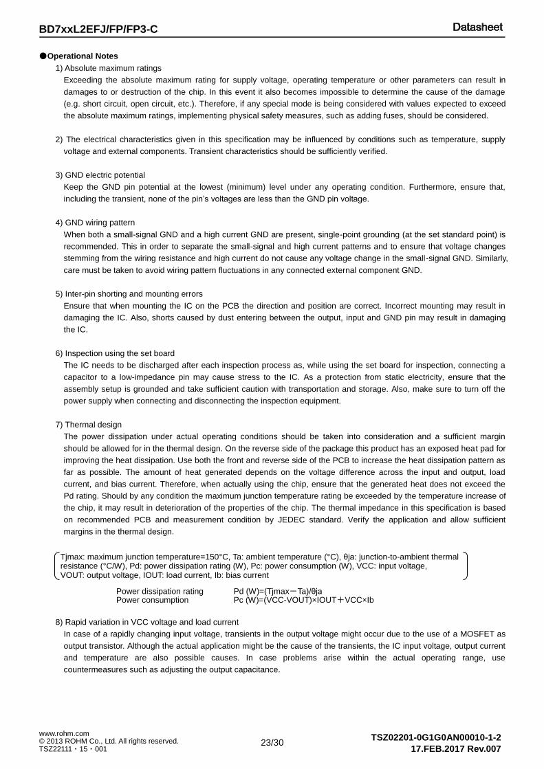
Tjmax: maximum junction temperature=150°C, Ta: ambient temperature (°C), θja: junction-to-ambient thermal resistance (°C/W), Pd: power dissipation rating (W), Pc: power consumption (W), VCC: input voltage, VOUT: output voltage, IOUT: load current, Ib: bias current
Power dissipation rating Pd (W)=(Tjmax-Ta)/θja Power consumption Pc (W)=(VCC-VOUT)×IOUT+VCC×Ib
8) Rapid variation in VCC voltage and load current
In case of a rapidly changing input voltage, transients in the output voltage might occur due to the use of a MOSFET as
output transistor. Although the actual application might be the cause of the transients, the IC input voltage, output current
and temperature are also possible causes. In case problems arise within the actual operating range, use
countermeasures such as adjusting the output capacitance.
.
24/30
TSZ02201-0G1G0AN00010-1-2 © 2013 ROHM Co., Ltd. All rights reserved. TSZ22111・15・001
www.rohm.com
BD7xxL2EFJ/FP/FP3-C
17.FEB.2017 Rev.007
9) Minute variation in output voltage
In case of using an application susceptible to minute changes to the output voltage due to noise, changes in input and
load current, etc., use countermeasures such as implementing filters.
10) Overcurrent protection circuit
This IC incorporates an integrated overcurrent protection circuit that is activated when the load is shorted. This protection
circuit is effective in preventing damage due to sudden and unexpected incidents. However, the IC should not be used in
applications characterized by continuous operation or transitioning of the protection circuit.
11) Thermal shutdown (TSD)
This IC incorporates and integrated thermal shutdown circuit to prevent heat damage to the IC. Normal operation should
be within the power dissipation rating, if however the rating is exceeded for a continued period, the junction temperature
(Tj) will rise and the TSD circuit will be activated and turn all output pins OFF. After the Tj falls below the TSD threshold
the circuits are automatically restored to normal operation.
Note that the TSD circuit operates in a situation that exceeds the absolute maximum ratings and therefore, under no
circumstances, should the TSD circuit be used in a set design or for any purpose other than protecting the IC from heat
damage.
12) In some applications, the VCC and pin potential might be reversed, possibly resulting in circuit internal damage or
damage to the elements. For example, while the external capacitor is charged, the VCC shorts to the GND. Use a
capacitor with a capacitance with less than 1000μF. We also recommend using reverse polarity diodes in series or a
bypass between all pins and the VCC pin.
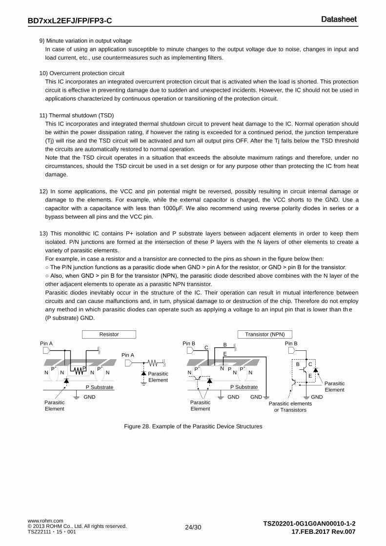
13) This monolithic IC contains P+ isolation and P substrate layers between adjacent elements in order to keep them
isolated. P/N junctions are formed at the intersection of these P layers with the N layers of other elements to create a
variety of parasitic elements.
For example, in case a resistor and a transistor are connected to the pins as shown in the figure below then:
○ The P/N junction functions as a parasitic diode when GND > pin A for the resistor, or GND > pin B for the transistor.
○ Also, when GND > pin B for the transistor (NPN), the parasitic diode described above combines with the N layer of the
other adjacent elements to operate as a parasitic NPN transistor.
Parasitic diodes inevitably occur in the structure of the IC. Their operation can result in mutual interference between
circuits and can cause malfunctions and, in turn, physical damage to or destruction of the chip. Therefore do not employ
any method in which parasitic diodes can operate such as applying a voltage to an input pin that is lower than th e
(P substrate) GND.
Figure 28. Example of the Parasitic Device Structures
N NP
+ PN N
P+
P Substrate
Parasitic
Element
GND
NP
+
N NP
+N P
P Substrate
GND GND
Parasitic
Element
Pin A
Pin A
Pin B Pin B
B C
E
Parasitic
Element
GND
Parasitic elements
or Transistors
Parasitic
Element
CB
E
Transistor (NPN)Resistor
.
25/30
TSZ02201-0G1G0AN00010-1-2 © 2013 ROHM Co., Ltd. All rights reserved. TSZ22111・15・001
www.rohm.com
BD7xxL2EFJ/FP/FP3-C
17.FEB.2017 Rev.007
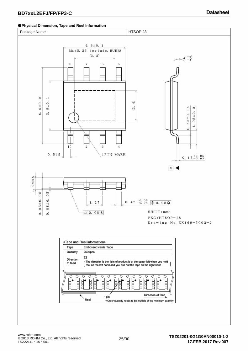
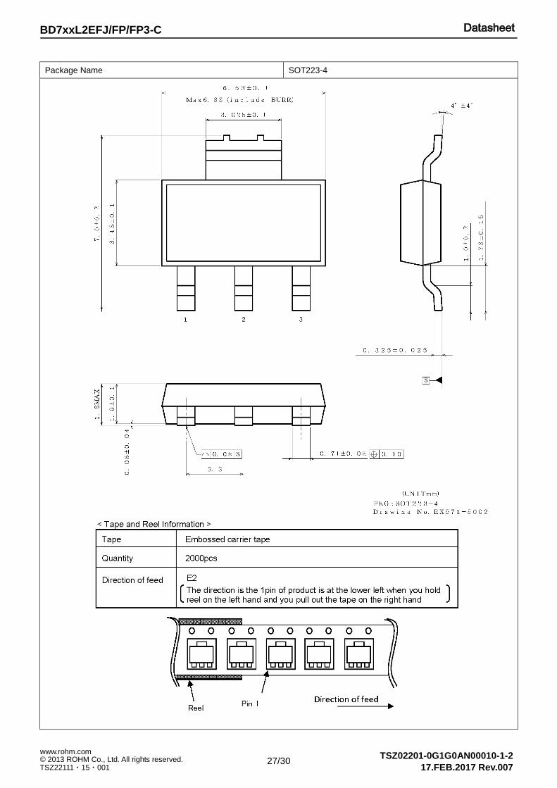
●Physical Dimension, Tape and Reel Information
Package Name HTSOP-J8
.
26/30
TSZ02201-0G1G0AN00010-1-2 © 2013 ROHM Co., Ltd. All rights reserved. TSZ22111・15・001
www.rohm.com
BD7xxL2EFJ/FP/FP3-C
17.FEB.2017 Rev.007
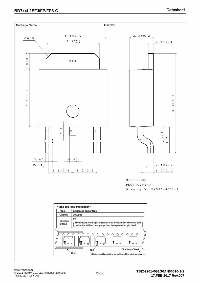
Package Name TO252-3
.
27/30
TSZ02201-0G1G0AN00010-1-2 © 2013 ROHM Co., Ltd. All rights reserved. TSZ22111・15・001
www.rohm.com
BD7xxL2EFJ/FP/FP3-C
17.FEB.2017 Rev.007
Package Name SOT223-4
.
28/30
TSZ02201-0G1G0AN00010-1-2 © 2013 ROHM Co., Ltd. All rights reserved. TSZ22111・15・001
www.rohm.com
BD7xxL2EFJ/FP/FP3-C
17.FEB.2017 Rev.007
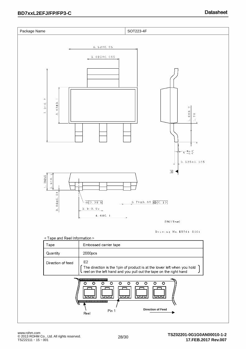
Package Name SOT223-4F
Direction of Feed
.
29/30
TSZ02201-0G1G0AN00010-1-2 © 2013 ROHM Co., Ltd. All rights reserved. TSZ22111・15・001
www.rohm.com
BD7xxL2EFJ/FP/FP3-C
17.FEB.2017 Rev.007
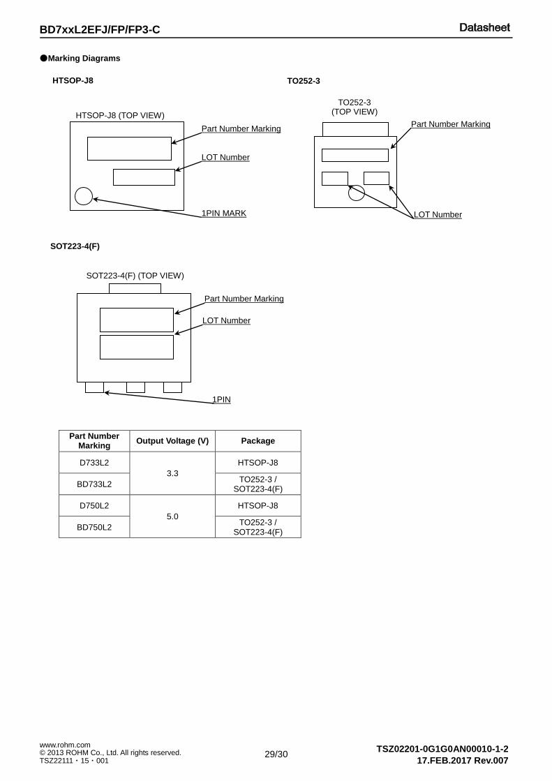
●Marking Diagrams
Part Number Marking
Output Voltage (V) Package
D733L2
3.3
HTSOP-J8
BD733L2 TO252-3 /
SOT223-4(F)
D750L2
5.0
HTSOP-J8
BD750L2 TO252-3 /
SOT223-4(F)
TO252-3 HTSOP-J8
HTSOP-J8 (TOP VIEW)
Part Number Marking
LOT Number
1PIN MARK
TO252-3 (TOP VIEW)
Part Number Marking
LOT Number
SOT223-4(F) (TOP VIEW)
Part Number Marking
LOT Number
1PIN
SOT223-4(F)
.
30/30
TSZ02201-0G1G0AN00010-1-2 © 2013 ROHM Co., Ltd. All rights reserved. TSZ22111・15・001
www.rohm.com
BD7xxL2EFJ/FP/FP3-C
17.FEB.2017 Rev.007
●Revision History
Date Revision Changes
21.Aug.2012 001 New Release
24.Sep.2012 002 New Release TO252-3 package.
14.Mar.2013 003
Page 1.Series name is changed. Page 6. Append Thermal Resistance θja, θjc. Page 8. Figure 5, Page 9. Figure 11 All Quiescent current are integrated into Bias Current. Page 10. Figure 14, Page 11. Figure 15 All Quiescent current are integrated into Bias Current. Page 12. Figure 21, Page 13. Figure 24 All Quiescent current are integrated into Bias Current. Page 17, 18. Figure 25, 26, 27, 28
Power Dissipation is changed to be compliant with JEDEC standard. Page 19, 20. Calculation examples are changed. Page 25. “Application example” is deleted. Figure 29 “ Example of the Parasitic Device Structures” is renewed.
30.Sep.2013 004 AEC-Q100 Qualified Page 28. Physical Quantity is changed.
01.May.2014 005 TO263-3F is changed to the individual registration.
14.Jul.2014 006 Page 16. Output capacitor range was changed. Page 28. HTSOP-J8 Marking Diagrams is changed.
17.Feb.2017 007
Improve the description, SOT223-4F to SOT223-4(F). Page 1. AEC-Q100 Grade postscript. Page 6. Thermal resistance is changed for JESD51-2A. Page 10. Revised Figure 13. Page 17, 18. Value of the power dissipation is changed. Page 23. Revised 7) in Operational Notes with change of Thermal resistance. Page 27. Add Physical Dimension, Tape and Reel Information of SOT223-4 package.

Notice-PAA-E Rev.003
© 2015 ROHM Co., Ltd. All rights reserved.
Notice
Precaution on using ROHM Products 1. If you intend to use our Products in devices requiring extremely high reliability (such as medical equipment
(Note 1),
aircraft/spacecraft, nuclear power controllers, etc.) and whose malfunction or failure may cause loss of human life, bodily injury or serious damage to property (“Specific Applications”), please consult with the ROHM sales representative in advance. Unless otherwise agreed in writing by ROHM in advance, ROHM shall not be in any way responsible or liable for any damages, expenses or losses incurred by you or third parties arising from the use of any ROHM’s Products for Specific Applications.
(Note1) Medical Equipment Classification of the Specific Applications
JAPAN USA EU CHINA
CLASSⅢ CLASSⅢ
CLASSⅡb CLASSⅢ
CLASSⅣ CLASSⅢ
2. ROHM designs and manufactures its Products subject to strict quality control system. However, semiconductor
products can fail or malfunction at a certain rate. Please be sure to implement, at your own responsibilities, adequate safety measures including but not limited to fail-safe design against the physical injury, damage to any property, which a failure or malfunction of our Products may cause. The following are examples of safety measures:
[a] Installation of protection circuits or other protective devices to improve system safety [b] Installation of redundant circuits to reduce the impact of single or multiple circuit failure
3. Our Products are not designed under any special or extraordinary environments or conditions, as exemplified below. Accordingly, ROHM shall not be in any way responsible or liable for any damages, expenses or losses arising from the use of any ROHM’s Products under any special or extraordinary environments or conditions. If you intend to use our Products under any special or extraordinary environments or conditions (as exemplified below), your independent verification and confirmation of product performance, reliability, etc, prior to use, must be necessary:
[a] Use of our Products in any types of liquid, including water, oils, chemicals, and organic solvents [b] Use of our Products outdoors or in places where the Products are exposed to direct sunlight or dust [c] Use of our Products in places where the Products are exposed to sea wind or corrosive gases, including Cl2,
H2S, NH3, SO2, and NO2
[d] Use of our Products in places where the Products are exposed to static electricity or electromagnetic waves [e] Use of our Products in proximity to heat-producing components, plastic cords, or other flammable items [f] Sealing or coating our Products with resin or other coating materials [g] Use of our Products without cleaning residue of flux (even if you use no-clean type fluxes, cleaning residue of
flux is recommended); or Washing our Products by using water or water-soluble cleaning agents for cleaning residue after soldering
[h] Use of the Products in places subject to dew condensation
4. The Products are not subject to radiation-proof design. 5. Please verify and confirm characteristics of the final or mounted products in using the Products. 6. In particular, if a transient load (a large amount of load applied in a short period of time, such as pulse. is applied,
confirmation of performance characteristics after on-board mounting is strongly recommended. Avoid applying power exceeding normal rated power; exceeding the power rating under steady-state loading condition may negatively affect product performance and reliability.
7. De-rate Power Dissipation depending on ambient temperature. When used in sealed area, confirm that it is the use in
the range that does not exceed the maximum junction temperature. 8. Confirm that operation temperature is within the specified range described in the product specification. 9. ROHM shall not be in any way responsible or liable for failure induced under deviant condition from what is defined in
this document.
Precaution for Mounting / Circuit board design 1. When a highly active halogenous (chlorine, bromine, etc.) flux is used, the residue of flux may negatively affect product
performance and reliability. 2. In principle, the reflow soldering method must be used on a surface-mount products, the flow soldering method must
be used on a through hole mount products. If the flow soldering method is preferred on a surface-mount products, please consult with the ROHM representative in advance.
For details, please refer to ROHM Mounting specification

Notice-PAA-E Rev.003
© 2015 ROHM Co., Ltd. All rights reserved.
Precautions Regarding Application Examples and External Circuits 1. If change is made to the constant of an external circuit, please allow a sufficient margin considering variations of the
characteristics of the Products and external components, including transient characteristics, as well as static characteristics.
2. You agree that application notes, reference designs, and associated data and information contained in this document
are presented only as guidance for Products use. Therefore, in case you use such information, you are solely responsible for it and you must exercise your own independent verification and judgment in the use of such information contained in this document. ROHM shall not be in any way responsible or liable for any damages, expenses or losses incurred by you or third parties arising from the use of such information.
Precaution for Electrostatic This Product is electrostatic sensitive product, which may be damaged due to electrostatic discharge. Please take proper caution in your manufacturing process and storage so that voltage exceeding the Products maximum rating will not be applied to Products. Please take special care under dry condition (e.g. Grounding of human body / equipment / solder iron, isolation from charged objects, setting of Ionizer, friction prevention and temperature / humidity control).
Precaution for Storage / Transportation 1. Product performance and soldered connections may deteriorate if the Products are stored in the places where:
[a] the Products are exposed to sea winds or corrosive gases, including Cl2, H2S, NH3, SO2, and NO2 [b] the temperature or humidity exceeds those recommended by ROHM [c] the Products are exposed to direct sunshine or condensation [d] the Products are exposed to high Electrostatic
2. Even under ROHM recommended storage condition, solderability of products out of recommended storage time period may be degraded. It is strongly recommended to confirm solderability before using Products of which storage time is exceeding the recommended storage time period.
3. Store / transport cartons in the correct direction, which is indicated on a carton with a symbol. Otherwise bent leads
may occur due to excessive stress applied when dropping of a carton. 4. Use Products within the specified time after opening a humidity barrier bag. Baking is required before using Products of
which storage time is exceeding the recommended storage time period.
Precaution for Product Label A two-dimensional barcode printed on ROHM Products label is for ROHM’s internal use only.
Precaution for Disposition When disposing Products please dispose them properly using an authorized industry waste company.
Precaution for Foreign Exchange and Foreign Trade act Since concerned goods might be fallen under listed items of export control prescribed by Foreign exchange and Foreign trade act, please consult with ROHM in case of export.
Precaution Regarding Intellectual Property Rights 1. All information and data including but not limited to application example contained in this document is for reference
only. ROHM does not warrant that foregoing information or data will not infringe any intellectual property rights or any other rights of any third party regarding such information or data.
2. ROHM shall not have any obligations where the claims, actions or demands arising from the combination of the Products with other articles such as components, circuits, systems or external equipment (including software).
3. No license, expressly or implied, is granted hereby under any intellectual property rights or other rights of ROHM or any third parties with respect to the Products or the information contained in this document. Provided, however, that ROHM will not assert its intellectual property rights or other rights against you or your customers to the extent necessary to manufacture or sell products containing the Products, subject to the terms and conditions herein.
Other Precaution 1. This document may not be reprinted or reproduced, in whole or in part, without prior written consent of ROHM.
2. The Products may not be disassembled, converted, modified, reproduced or otherwise changed without prior written consent of ROHM.
3. In no event shall you use in any way whatsoever the Products and the related technical information contained in the Products or this document for any military purposes, including but not limited to, the development of mass-destruction weapons.
4. The proper names of companies or products described in this document are trademarks or registered trademarks of ROHM, its affiliated companies or third parties.
DatasheetDatasheet
Notice – WE Rev.001© 2015 ROHM Co., Ltd. All rights reserved.
General Precaution 1. Before you use our Pro ducts, you are requested to care fully read this document and fully understand its contents.
ROHM shall n ot be in an y way responsible or liabl e for fa ilure, malfunction or acci dent arising from the use of a ny ROHM’s Products against warning, caution or note contained in this document.
2. All information contained in this docume nt is current as of the issuing date and subj ect to change without any prior
notice. Before purchasing or using ROHM’s Products, please confirm the la test information with a ROHM sale s representative.
3. The information contained in this doc ument is provi ded on an “as is” basis and ROHM does not warrant that all
information contained in this document is accurate an d/or error-free. ROHM shall not be in an y way responsible or liable for any damages, expenses or losses incurred by you or third parties resulting from inaccuracy or errors of or concerning such information.


![[XLS] · Web viewEVERGREEN MARINE CO. INFODEMA S.A. 1270 X 2500 MM LOS DEMAS PAPELES IMPREGANDOSD E PLASTICO NO ADHESIVO DE 220MM X 889MM X 76.2MM EN ROLLOS DE 15 GSM JORGE AIACH](https://img.pdfslide.tips/doc/110x75/5b0240fc7f8b9ab9598d867a/xls-viewevergreen-marine-co-infodema-sa-1270-x-2500-mm-los-demas-papeles-impregandosd.jpg)