Embed Size (px)
Citation preview

PFS7623-7629/7633-7636HiperPFS-4 Family
www.power.com January 2017
PFC Controller with Integrated 600 V MOSFET Optimized for High PF and Efficiency Across Load Range
Key Benefits
• Integrated 600 V MOSFET• High efficiency and power factor across load range
• >95% efficiency from 10% load to 100% load• <60 mW no-load consumption at 230 VAC• PF >0.95 achievable at 20% load• EN61000-3-2 Class C and D compliant
• Highly integrated for smallest boost PFC form factor• Packaging optimized for high volume production• Eliminates insulating pad/heat-spreader• Programmable Power Good (PG) signal• User selectable power limit: Enables different HiperPFS-4 family
members to be tested in the same design for optimum device selection
• Integrated non-linear amplifier for fast output OV and UV protection and transient response
• Digital line peak detection for robust performance even with distorted input voltage from UPS or generators
• Digital power factor enhancer compensates for EMI filter and bridge distortion, providing high-line PF >0.95 @ 20% load
• Frequency adjusted over line voltage and thru each line cycle• Spread-spectrum across >60 kHz window simplifies EMI filtering• Reduces boost inductance
• Provides up to 450 W peak output power for universal applications, 610 W for high-line only applications
• Protection features include: UVLO, UV, OV, OTP, brown-in/out, cycle-by-cycle current limit and power limiting for overload protection
• Withstands 305 VAC steady-state and 410 VAC abnormal input• Halogen free and RoHS compliant
Applications• PC • High-power adaptors• Printer • High-power LED lighting• LCD TV • Industrial and appliance• Video game consoles • Generic PFC converters• 80 Plus™ Platinum
designs
Figure 1. Typical Application Schematic.
This Product is Covered by Patents and/or Pending Patent Applications.
PI-7965-051616
ACIN
DCOUT
+
S
D
C
PGT
FB
VCC
PG
REFGV
CONTROL
HiperPFS-4
VCC
Figure 2. Package Options (Body Dimensions: 16.53 mm Width x 8.25 mm Height.)
eSIP-16D (H Package) eSIP-16G (L Package)
Output Power Table (Full Power Mode)
Universal Input Devices
ProductContinuous
Output Power at90 VAC
Peak Output Power
PFS7623H/L 110 W 120 W
PFS7624H/L 130 W 150 W
PFS7625H/L 185 W 205 W
PFS7626H 230 W 260 W
PFS7627H 290 W 320 W
PFS7628H 350 W 385 W
PFS7629H 405 W 450 W
High-Line Input Only Devices
ProductContinuous
Output Power at180 VAC
Peak Output Power
PFS7633H 255 W 280 W
PFS7634H 315 W 350 W
PFS7635H 435 W 480 W
PFS7636H 550 W 610 W
Table 1. Output Power Table (See Table 2 on page 10 for more information.)
Rev. A 01/17
2
PFS7623-7629/7633-7636
www.power.com
Description
The HiperPFS™-4 devices incorporate a continuous conduction mode (CCM) boost PFC controller, gate driver and 600 V power MOSFET in a single, low-profile (GROUND pin connected) power package. HiperPFS-4 devices eliminate need for external current sense resistors and their associated power loss, and use an innovative control technique that adjusts the switching frequency over output load, input line voltage, and input line cycle.
This control technique maximizes efficiency over the entire load range, particularly at light loads. Additionally, it minimizes the EMI filtering requirements due to its wide bandwidth spread spectrum effect. The HiperPFS-4 uses advanced digital techniques for line monitoring, line feed-forward scaling, and power factor enhancement; while using analog techniques for the core controller in order to maintain extremely low no-load power consumption. The HiperPFS-4 also features an integrated non-linear error amplifier for enhanced load transient response, a user programmable Power Good (PG) signal as well as user selectable power limit functionality. HiperPFS-4 includes Power Integrations’ standard set of comprehensive protection features, such as UV, OV, brown-in/out, and hysteretic thermal shutdown. HiperPFS-4 also provides cycle-by-cycle current limit and Safe Operating Area (SOA) protection of the power MOSFET, output power limiting for overload protection, and pin-to-pin short-circuit protection
HiperPFS-4’s innovative variable frequency continuous conduction mode operation (VF-CCM) minimizes switching losses by maintaining a low average switching frequency, while modulating the switching frequency in order to suppress EMI, the traditional challenge with continuous conduction mode solutions. Systems using HiperPFS-4 typically reduce the total X and Y capacitance requirements of the converter, the inductance of both the boost choke and EMI noise suppression chokes, thereby reducing overall system size and cost. Additionally, HiperPFS-4 devices dramatically reduce component count and board footprint while simplifying system design and enhancing reliability, when compared with designs that use discrete MOSFETs and controllers. The innovative variable frequency, continuous conduction mode controller enables the HiperPFS-4 to realize all of the benefits of continuous conduction mode operation while leveraging low-cost, small, simple EMI filters.
Many regions mandate high power factor for many electronic products with high power requirements. These rules are combined with numerous application-specific standards that require high power supply efficiency across the entire load range, from full load to as low as 10% load. High efficiency at light load is a challenge for traditional PFC solutions where fixed MOSFET switching frequencies cause fixed switching losses on each cycle, even at light loads. In addition to featuring flat efficiency across the load range, HiperPFS-4 also enables a high power factor of >0.95 at 20% load. HiperPFS-4 simplifies compliance with new and emerging energy-efficiency standards over a broad market space in applications such as PCs, LCD TVs, notebooks, appliances, pumps, motors, fans, printers and LED lighting.
HiperPFS-4’s advanced power packaging technology and high efficiency simplify the complexity of mounting the IC and thermal management, while providing very high power capabilities in a single compact package; these devices are suitable for PFC applications with maximum continuous power from 75 W to 405 W universal (550 W high-line only).
Product HighlightsProtected Power Factor Correction Solution• Incorporates 600 V power MOSFET, controller and gate driver.• EN61000-3-2 Class C and Class D compliance.• Integrated protection features reduce external component count
• Accurate built-in brown-in/out protection.• Accurate built-in undervoltage (UV) protection.• Accurate built-in overvoltage (OV) protection.• Hysteretic thermal shutdown (OTP).• Internal power limiting function for overload protection.• Cycle-by-cycle power-switch current limit.• Internal non-linear error amplifier for enhanced load transient
response• No external current sense resistor required.
• Provides ‘lossless’ internal sensing via sense-FET.• Reduces component count and system losses.• Minimizes high current gate drive loop area.
• Minimizes output overshoot and stresses during start-up• Integrated power limit.
• Improved dynamic response.• Digitally controlled input line feed-forward gain adjustment for
flattened loop gain across entire input voltage range.• Eliminates up to 39 discrete components for higher reliability and
lower cost.Solution for High Efficiency, Low EMI and High PF• Continuous conduction mode PFC uses novel constant amp-second
[on-time] volt-second [off-time] control.• High efficiency across load.• High power factor across load.
• Frequency sliding technique for light load efficiency improvements.• >95% efficiency from 10% load to full load achievable at
nominal input voltages.• Variable switching frequency to simplify EMI filter design.
• Varies over line input voltage to maximize efficiency and minimize EMI filter requirements.
• Varies with input line cycle voltage by >60 kHz to maximize spread spectrum effect.
Advanced Package for High Power Applications• Up to 450 W [universal], 610 W [high-line only] peak output power
capability in a highly compact package.• Simple adhesive or clip mounting to heat sink.
• No insulation pad required and can be directly connected to heat sink.
• Staggered pin arrangement allows simple routing of board traces and to meet high-voltage creepage requirements.
• Single package solution for PFC converter reduces assembly costs and layout size.
Rev. A 01/17
3
PFS7623-7629/7633-7636
www.power.com
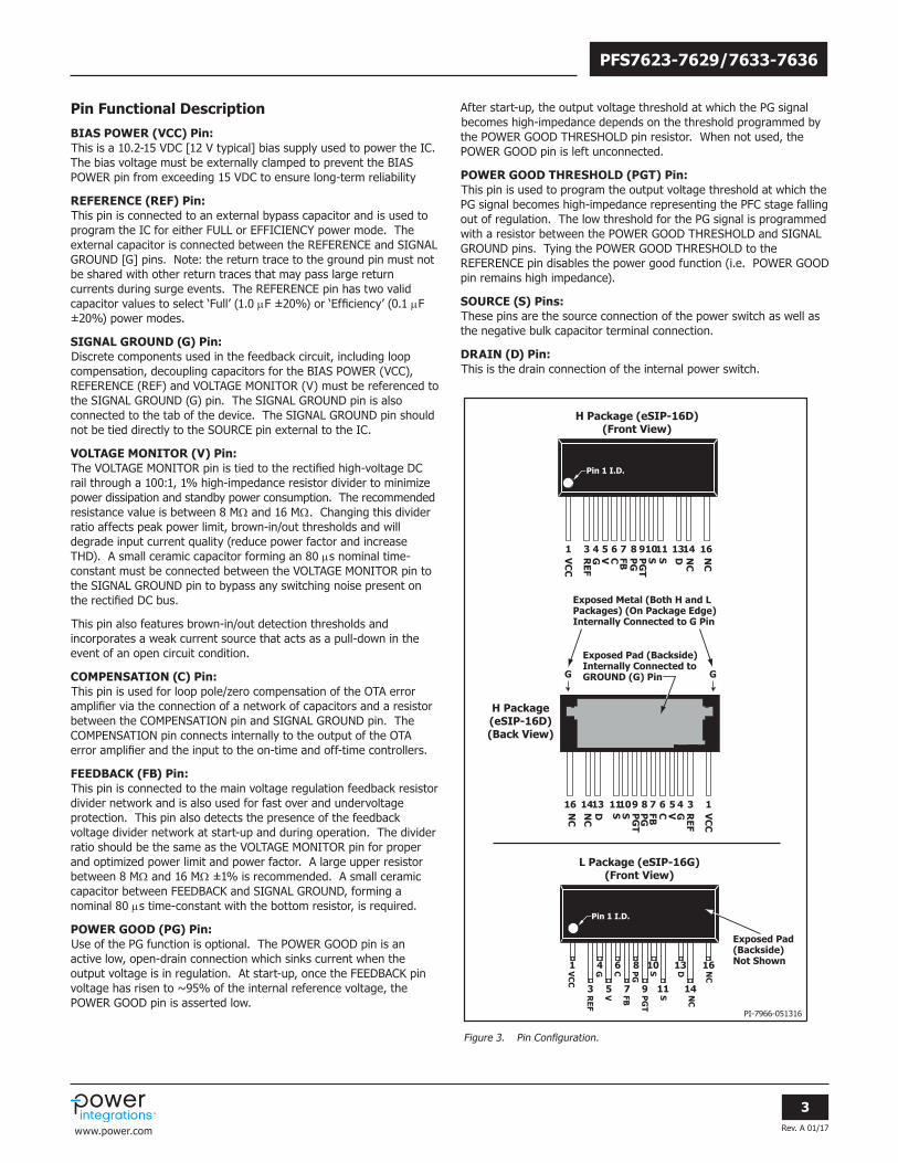
Pin Functional Description
BIAS POWER (VCC) Pin:This is a 10.2-15 VDC [12 V typical] bias supply used to power the IC. The bias voltage must be externally clamped to prevent the BIAS POWER pin from exceeding 15 VDC to ensure long-term reliability
REFERENCE (REF) Pin:This pin is connected to an external bypass capacitor and is used to program the IC for either FULL or EFFICIENCY power mode. The external capacitor is connected between the REFERENCE and SIGNAL GROUND [G] pins. Note: the return trace to the ground pin must not be shared with other return traces that may pass large return currents during surge events. The REFERENCE pin has two valid capacitor values to select ‘Full’ (1.0 mF ±20%) or ‘Efficiency’ (0.1 mF ±20%) power modes.
SIGNAL GROUND (G) Pin:Discrete components used in the feedback circuit, including loop compensation, decoupling capacitors for the BIAS POWER (VCC), REFERENCE (REF) and VOLTAGE MONITOR (V) must be referenced to the SIGNAL GROUND (G) pin. The SIGNAL GROUND pin is also connected to the tab of the device. The SIGNAL GROUND pin should not be tied directly to the SOURCE pin external to the IC.
VOLTAGE MONITOR (V) Pin:The VOLTAGE MONITOR pin is tied to the rectified high-voltage DC rail through a 100:1, 1% high-impedance resistor divider to minimize power dissipation and standby power consumption. The recommended resistance value is between 8 MW and 16 MW. Changing this divider ratio affects peak power limit, brown-in/out thresholds and will degrade input current quality (reduce power factor and increase THD). A small ceramic capacitor forming an 80 ms nominal time-constant must be connected between the VOLTAGE MONITOR pin to the SIGNAL GROUND pin to bypass any switching noise present on the rectified DC bus.
This pin also features brown-in/out detection thresholds and incorporates a weak current source that acts as a pull-down in the event of an open circuit condition.
COMPENSATION (C) Pin:This pin is used for loop pole/zero compensation of the OTA error amplifier via the connection of a network of capacitors and a resistor between the COMPENSATION pin and SIGNAL GROUND pin. The COMPENSATION pin connects internally to the output of the OTA error amplifier and the input to the on-time and off-time controllers.
FEEDBACK (FB) Pin:This pin is connected to the main voltage regulation feedback resistor divider network and is also used for fast over and undervoltage protection. This pin also detects the presence of the feedback voltage divider network at start-up and during operation. The divider ratio should be the same as the VOLTAGE MONITOR pin for proper and optimized power limit and power factor. A large upper resistor between 8 MW and 16 MW ±1% is recommended. A small ceramic capacitor between FEEDBACK and SIGNAL GROUND, forming a nominal 80 ms time-constant with the bottom resistor, is required.
POWER GOOD (PG) Pin:Use of the PG function is optional. The POWER GOOD pin is an active low, open-drain connection which sinks current when the output voltage is in regulation. At start-up, once the FEEDBACK pin voltage has risen to ~95% of the internal reference voltage, the POWER GOOD pin is asserted low.
After start-up, the output voltage threshold at which the PG signalbecomes high-impedance depends on the threshold programmed by the POWER GOOD THRESHOLD pin resistor. When not used, the POWER GOOD pin is left unconnected.
POWER GOOD THRESHOLD (PGT) Pin:This pin is used to program the output voltage threshold at which the PG signal becomes high-impedance representing the PFC stage falling out of regulation. The low threshold for the PG signal is programmed with a resistor between the POWER GOOD THRESHOLD and SIGNAL GROUND pins. Tying the POWER GOOD THRESHOLD to the REFERENCE pin disables the power good function (i.e. POWER GOOD pin remains high impedance).
SOURCE (S) Pins:These pins are the source connection of the power switch as well as the negative bulk capacitor terminal connection.
DRAIN (D) Pin:This is the drain connection of the internal power switch.
PI-7966-051316
H Package (eSIP-16D)(Front View)
H Package(eSIP-16D)(Back View)
L Package (eSIP-16G)(Front View)
16VC
C
REF
G V C FB PG
PG
T
D NC
16NC
SS 13
D13
NC
14
NC
14
11
S11
9
PG
T
9
10
S10
8
PG
8
1
VC
C
1
3
REF
3
4
G4
5
V5
6
C6
7
FB
7
Exposed Pad (Backside)Internally Connected to GROUND (G) Pin
Exposed Metal (Both H and L Packages) (On Package Edge) Internally Connected to G Pin
1
3
4
5
6
7
8
9
10
11
13
14
16
Pin 1 I.D.
Pin 1 I.D.
G G
VC
C
REF
GV
CFB
PG
PG
T
D NC
SS
NC
Exposed Pad(Backside)Not Shown
Figure 3. Pin Configuration.
Rev. A 01/17
4
PFS7623-7629/7633-7636
www.power.com
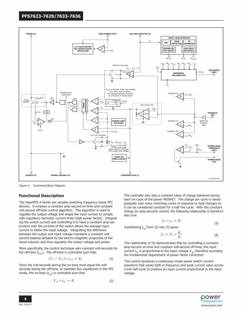
Figure 4. Functional Block Diagram.
PI-7969-051316
+
-
+
-
BIAS POWER (VCC)DRAIN (D)
SOURCE (S) SIGNAL GROUND (G)
POWER GOOD(PG)
POWER GOODTHRESHOLD
(PGT)
REFERENCE(REF)
FEEDBACK(FB)
UVLO
12 V GATE DRIVERREF SERIES/SHUNT
REGULATOR
REFERENCEAND BAND GAP
VOLTAGE MONITOR (V)
HL/LL MON(PFE)
INPUT LINE INTERFACE
ADCPEAK
DETECTORPF
ENHANCER
LOW/HIGHLINE DETECT
BROWN-IN/OUT DETECT
BO, BI
VV
+
-
+
-
+
-
+
-
+
-
+
-
COMPENSATION (C)
VBRST
~(VO-VIN)
FBREF
FEEDBACK PinOV/UV/OFF
Off-Time Controller
On-Time Controller
senseFETPower
MOSFET
Feedback UV Buffer andDe-Glitch
Filter
Feedback OFF
MOFF × (VFB - VV)
CINT
PON
FBREF VPG(H) FBUV FBOFF IOCPFBOV
IPGT
FBOV
+
-
+
-
FBUV
+
-
FBOFF
+
-
VFBVPG(H)
REF
IPGT
IOCP
ISNS
VOFF
VE
VBRST
CINT
HL/LL
V OFF
VE
PON × MON(PFE) × ISNS
VCC Latch
START-UP,FMEA CHECKS
POWER LIMITSOA RAMP
TIM
ERSU
PER
VIS
OR Frequency
Slide
MON(PFE) is the switchcurrent sense scale
factor which is a functionof the peak input voltage
OCP
HL/LL
LEB
Feedback OV
Non-Linear OTA
OTA
VOFF is a function of the error-voltage(VE) and is used to reduce
the average operating frequencyas a function of output power
VCC
Functional Description
The HiperPFS-4 family are variable switching frequency boost PFC devices. It employs a constant amp-second on-time and constant volt-second off-time control algorithm. This algorithm is used to regulate the output voltage and shape the input current to comply with regulatory harmonic current limits (high power factor). Integrat-ing the switch current and controlling it to have a constant amp-sec product over the on-time of the switch allows the average input current to follow the input voltage. Integrating the difference between the output and input voltage maintains a constant volt-second balance dictated by the electro-magnetic properties of the boost inductor and thus regulates the output voltage and power.
More specifically, the control technique sets constant volt-seconds for the off-time (tOFF). The off-time is controlled such that:
#V V t KO IN OFF 1- =^ h (1)
Since the volt-seconds during the on-time must equal the volt- seconds during the off-time, to maintain flux equilibrium in the PFC choke, the on-time (tON) is controlled such that
#V t KIN ON 1= (2)
The controller also sets a constant value of charge delivered during each on-cycle of the power MOSFET. The charge per cycle is varied gradually over many switching cycles in response to load changes so it can be considered constant for a half line cycle. With this constant charge (or amp-second) control, the following relationship is therefore also true:
#I t KIN ON 2= (3)
Substituting tON from (2) into (3) gives: (4)
#I VKK
IN IN
1
2=
The relationship of (4) demonstrates that by controlling a constant amp-second on-time and constant volt-second off-time, the input current IIN is proportional to the input voltage VIN, therefore providing the fundamental requirement of power factor correction.
This control produces a continuous mode power switch current waveform that varies both in frequency and peak current value across a line half-cycle to produce an input current proportional to the input voltage.
Rev. A 01/17
5
PFS7623-7629/7633-7636
www.power.com
Control EngineThe controller features a low bandwidth, high gain OTA error-amplifier of which its non-inverting terminal is connected to an internal voltage reference of 3.85 V. The inverting terminal of the error-amplifier is available on the external FEEDBACK pin which connects to the output voltage divider network with a divider ratio of 1:100 to regulate the output voltage to 385 V nominally. The FEEDBACK pin connects directly to the divider network for fast transient load response.
The internally sensed FET switch current is scaled by the input voltage peak detector current sense gain (MON) then integrated and compared with the error-amplifier signal (VE) to determine the cycle on-time. Internally the difference between the input and output voltage is derived and the resultant is scaled, integrated, andcompared to a voltage reference (VOFF) to determine the cycle off-time. Careful selection of the internal scaling factors produce input current waveforms with very low distortion and high power factor.
Line Feed-Forward Scaling Factor (MON) and PF EnhancerThe VOLTAGE MONITOR (V) pin voltage is sampled and converted by a Δ-Σ ADC to a quantized digital value. A digital line cycle peak detector, with dynamic time constants and multi-cycle filtering, derives and smooths the peak of the input line voltage. This peak is used internally to scale the gain of the current sense signal through the MON variable. This contribution is required to reduce the dynamicrange of the control feedback signal as well as flatten the loop gain over the operating input line range. The line-sense feed-forward gain adjustment is proportional to the square of the peak rectified AC line voltage and is adjusted as a function of the VOLTAGE MONITOR pin voltage.
At high-line and light load, the feed-forward MON variable is dynami-cally adjusted across the line cycle in order to compensate for the line current distortion through the EMI filter and full bridge network, and improve power factor.
The line-sense feed-forward gain is also important in providing a switch power limit over the input line range.
This characteristic is optimized to maintain a relatively constant internal error-voltage level at full load from an input line of 90 to 230 VAC.
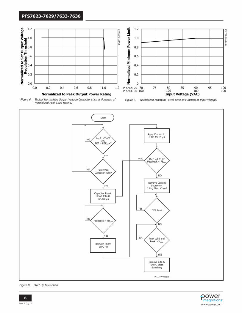
Beyond the specified peak power rating of the device, the internal power limit will regulate the output voltage below the set regulation threshold as a function of output overload to maintain constant output power. Figure 6 illustrates the typical regulation characteristic as a function of load.
Below the brown-in threshold (VBR+) the power limit is reduced when the device is operated in the ‘Full’ power mode as shown in Figure 7.As the input line voltage is reduced toward the brown-out threshold (VBR-) and if the load exceeds the power limit derating, the boostoutput voltage will drop out of regulation in accordance with Figure 6.
The rated peak power shown in Table 1 is not derated for voltages below the brown-in threshold when the device is operated in the ‘Efficiency’ mode.
Start-Up with Pin-to-Pin Short-Circuit ProtectionAt start-up, the engine performs a sequence of operational checksand pin short/open evaluations, as shown in Figure 8, prior to thecommencement of switching. When the input voltage peak is abovebrown-in, the engine enables switching.
The OTA error amplifier provides a non-linear amplifier (NLA)mechanism to overcome the inherently slow feedback loop responsewhen the sensed output voltage on the FEEDBACK pin is outside itsregulation window. This allows the error amplifier function to limitthe maximum overshoot and undershoot during load transient events.
To reduce switch and output diode current stress at start-up, theHiperPFS-4 calculates off-time based upon output voltage (VOUT) during start-up, resulting in a relatively soft controlled start-up.
Once the applied VCC is above the VCCUVLO+ threshold, and the output of the on-chip VREF regulator is above REFUV+, the value of the REFERENCE pin capacitor is detected and the full or efficiency power mode is latched. The pin open/short tests are performed, and if the FEEDBACK pin voltage is valid the over-temperature OTP is checked to be false. Once the preceding checks are satisfied the input voltage is monitored via the VOLTAGE MONITOR pin until it exceeds the VBR+ threshold [but the peak detector is not saturated]. It is at this point that switching is enabled.
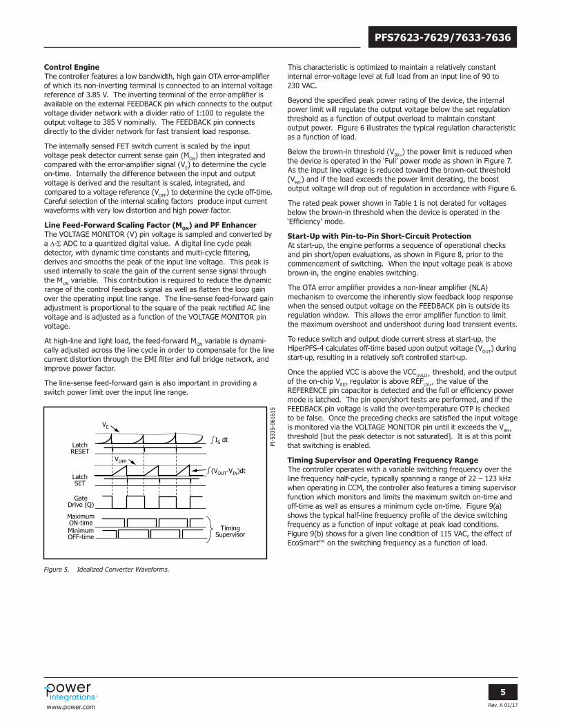
Timing Supervisor and Operating Frequency RangeThe controller operates with a variable switching frequency over the line frequency half-cycle, typically spanning a range of 22 – 123 kHz when operating in CCM, the controller also features a timing supervisor function which monitors and limits the maximum switch on-time and off-time as well as ensures a minimum cycle on-time. Figure 9(a) shows the typical half-line frequency profile of the device switching frequency as a function of input voltage at peak load conditions. Figure 9(b) shows for a given line condition of 115 VAC, the effect of EcoSmart™ on the switching frequency as a function of load.
Figure 5. Idealized Converter Waveforms.
PI-5
335-
0616
15
IS dt
VE
VOFF
(VOUT-VIN)dt
LatchRESET
LatchSET
GateDrive (Q)
MaximumON-timeMinimumOFF-time
TimingSupervisor
Rev. A 01/17
6
PFS7623-7629/7633-7636
www.power.com
Figure 8. Start-Up Flow Chart.
Figure 6. Typical Normalized Output Voltage Characteristics as Function of Normalized Peak Load Rating.
Figure 7. Normalized Minimum Power Limit as Function of Input Voltage.
0.0 0.2 0.4 0.6 1.0 1.20.8
Normalized to Peak Output Power Rating
Nor
mal
ized
to
Set
Ou
tpu
t V
olta
geR
egu
lati
on T
hre
shol
d1.2
1.0
0.8
0.6
0.4
0.2
0.0
PI-7
227-
0616
15
VCC > UVLO+and
REF > REFUV+?
YES
YES
NO
NO
NO
NO
PI-7249-061615
ReferenceCapacitor Valid?
Start
NO
YES
Capacitor Reset:Short C to Gfor 230 µs
YES
Feedback > FBOFF
Remove Short on C Pin
(C > 2.5 V) orFeedback < FBOFF
OTP Fault
Remove CurrentSource on
C Pin, Short C to G
YES
YES
NO
Apply Current to C Pin for 65 µs
Peak Valid andPeak > VBR+
Remove C to GShort, StartSwitching
70 75 80170
85 95 10090160 190
PFS7623-29PFS7633-39 180
Input Voltage (VAC)
Nor
mal
ized
Min
imum
Pow
er L
imit 1.2
1.0
0.8
0.6
0.4
0.2
0
PI-7
544a
-112
216
Rev. A 01/17
7
PFS7623-7629/7633-7636
www.power.com
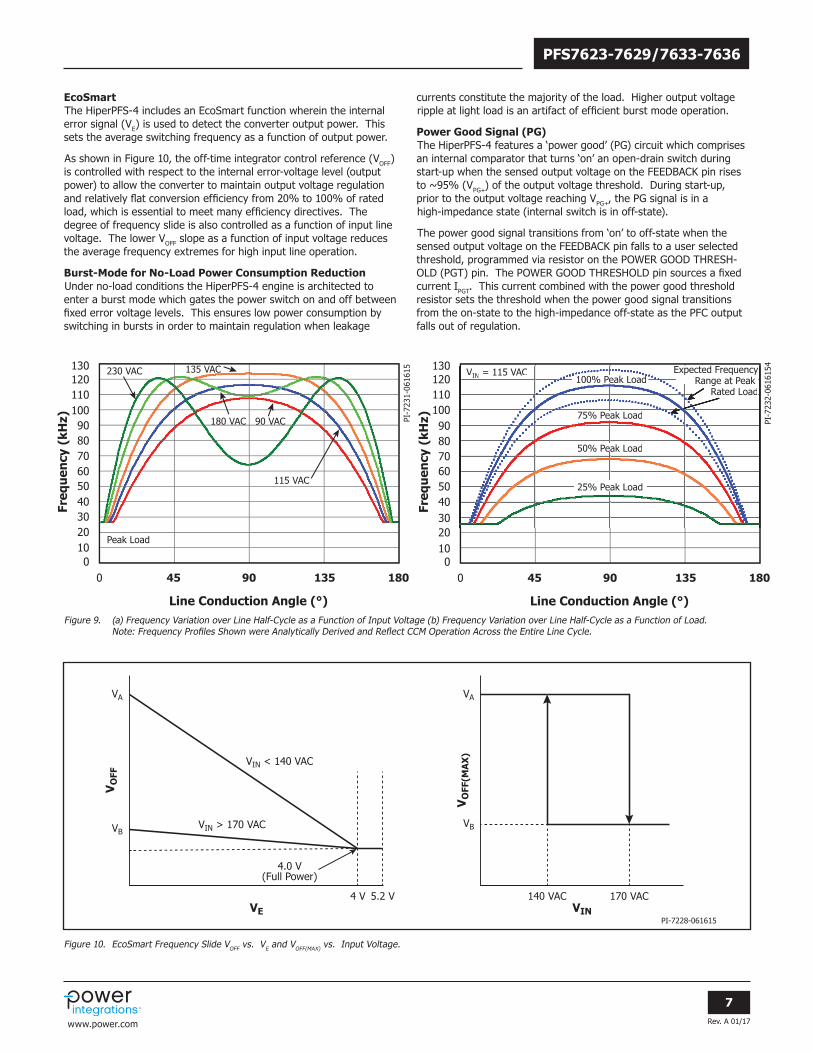
EcoSmartThe HiperPFS-4 includes an EcoSmart function wherein the internal error signal (VE) is used to detect the converter output power. This sets the average switching frequency as a function of output power.
As shown in Figure 10, the off-time integrator control reference (VOFF) is controlled with respect to the internal error-voltage level (output power) to allow the converter to maintain output voltage regulation and relatively flat conversion efficiency from 20% to 100% of rated load, which is essential to meet many efficiency directives. The degree of frequency slide is also controlled as a function of input line voltage. The lower VOFF slope as a function of input voltage reduces the average frequency extremes for high input line operation.
Burst-Mode for No-Load Power Consumption ReductionUnder no-load conditions the HiperPFS-4 engine is architected to enter a burst mode which gates the power switch on and off between fixed error voltage levels. This ensures low power consumption by switching in bursts in order to maintain regulation when leakage
currents constitute the majority of the load. Higher output voltageripple at light load is an artifact of efficient burst mode operation.
Power Good Signal (PG) The HiperPFS-4 features a ‘power good’ (PG) circuit which comprises an internal comparator that turns ‘on’ an open-drain switch during start-up when the sensed output voltage on the FEEDBACK pin rises to ~95% (VPG+) of the output voltage threshold. During start-up, prior to the output voltage reaching VPG+, the PG signal is in ahigh-impedance state (internal switch is in off-state).
The power good signal transitions from ‘on’ to off-state when the sensed output voltage on the FEEDBACK pin falls to a user selected threshold, programmed via resistor on the POWER GOOD THRESH-OLD (PGT) pin. The POWER GOOD THRESHOLD pin sources a fixed current IPGT. This current combined with the power good threshold resistor sets the threshold when the power good signal transitions from the on-state to the high-impedance off-state as the PFC output falls out of regulation.
Figure 9. (a) Frequency Variation over Line Half-Cycle as a Function of Input Voltage (b) Frequency Variation over Line Half-Cycle as a Function of Load. Note: Frequency Profiles Shown were Analytically Derived and Reflect CCM Operation Across the Entire Line Cycle.
0 45 90 135 180
PI-7
231-
0616
15130120
230 VAC
180 VAC
135 VAC
90 VAC
Peak Load
115 VAC
100110
9080706050403020100
Freq
uen
cy (
kHz)
Line Conduction Angle (°)
0 45 90 135 180
PI-7
232-
0616
154130
1201101009080706050403020100
Freq
uen
cy (
kHz)
Line Conduction Angle (°)
100% Peak Load
75% Peak Load
VIN = 115 VAC
25% Peak Load
50% Peak Load
Expected FrequencyRange at Peak
Rated Load100% Peak Loaddddddddddd
75% P k L d75% Peak Load
VIN = 115 VAC
25% Peak Load
50% Peak Loada50% Peak Load
Expected FrequencyRange at Peak
Rated Load
Figure 10. EcoSmart Frequency Slide VOFF vs. VE and VOFF(MAX) vs. Input Voltage.
VA
VIN < 140 VAC
4.0 V(Full Power)
VIN > 170 VAC
4 V 5.2 V 140 VAC 170 VAC
VA
VBVB
VO
FF
VE VIN
VO
FF(M
AX
)
PI-7228-061615
Rev. A 01/17
8
PFS7623-7629/7633-7636
www.power.com
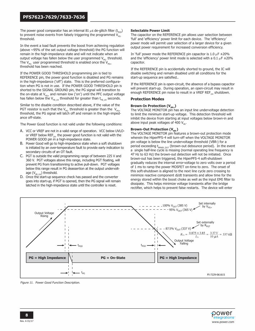
The power good comparator has an internal 81 ms de-glitch filter (tPGD) to prevent noise events from falsely triggering the programmed VPG- threshold.
In the event a load fault prevents the boost from achieving regulation (above ~95% of the set output voltage threshold) the PG function will remain in the high-impedance state and will not indicate when an output voltage has fallen below the user programmed VPG- threshold. The VPG- user programmed threshold is enabled once the VPG+ threshold has been reached.
If the POWER GOOD THRESHOLD programming pin is tied to REFERENCE pin, the power good function is disabled and PG remains in the high-impedance (‘off’) state. This is the preferred configura-tion when PG is not in use. If the POWER GOOD THRESHOLD pin is shorted to the SIGNAL GROUND pin, the PG signal will transition to the on-state at VPG+ and remain low (‘on’) until the PFC output voltage has fallen below the VFB_UV threshold for greater than tFB_UV seconds.
Similar to the disable condition described above, if the value of the PGT resistor is such that the VPG- threshold is greater than the VPG+ threshold, the PG signal will latch off and remain in the high-imped- ance off-state.
The Power Good function is not valid under the following conditions:
A. VCC or VREF are not in a valid range of operation. VCC below UVLO- or VREF below REFUV- the power good function is not valid with the POWER GOOD pin in a high-impedance state.
B. Power Good will go to high-impedance state when a soft shutdown is initiated by an over-temperature fault to provide early indication to secondary circuits of an OT fault.
C. PGT is outside the valid programming range of between 225 V and 360 V. PGT voltages above this range, including PGT floating, will prevent PG from transitionning to active pull-down. PGT voltages below this range result in PG deassertion at the output undervolt- age (VFB_UV) threshold.
D. Once the start-up sequence check has passed and the converter goes into start-up, if PGT is opened, then the PG signal will remain latched in the high-impedance state until the controller is reset.
Selectable Power LimitThe capacitor on the REFERENCE pin allows user selection between ’full’ and ‘efficiency’ power limit for each device. The ‘efficiency’ power mode will permit user selection of a larger device for a given output power requirement for increased conversion efficiency.
In ‘full’ power mode the REFERENCE pin capacitor is 1.0 mF ±20% and the ‘efficiency’ power limit mode is selected with a 0.1 mF ±20% capacitor.
If the REFERENCE pin is accidentally shorted to ground, the IC will disable switching and remain disabled until all conditions for the start-up sequence are satisfied..
If the REFERENCE pin is open-circuit, the absence of a bypass capacitor will prevent start-up. During operation, an open-circuit may result in enough REFERENCE pin noise to result in a VREF REFUV- shutdown.
Protection Modes
Brown-In Protection (VBR+)The VOLTAGE MONITOR pin has an input line undervoltage detectionto limit the minimum start-up voltage. This detection threshold will inhibit the device from starting at input voltages below brown-in and above input peak voltages of 400 VPK.
Brown-Out Protection (VBR-)The VOLTAGE MONITOR pin features a brown-out protection modewherein the HiperPFS-4 will turn-off when the VOLTAGE MONITOR pin voltage is below the line undervoltage threshold (VBR-) for a period exceeding tBRWN_OUT (brown-out debounce period). In the event a single half-line cycle is missing (normal operating line frequency is47 Hz to 63 Hz) the brown-out detection will not be initiated. Once brown-out has been triggered, the HiperPFS-4 soft-shutdown gradually reduces the internal error-voltage to zero volts over a period of 1 ms to ramp the power MOSFET on-time to zero. The onset of this soft-shutdown is aligned to the next line cycle zero crossing to minimize reactive component di/dt transients and allow time for the energy stored within the boost choke as well as the input EMI filter to dissipate. This helps minimize voltage transients after the bridge rectifier, which helps to prevent false restarts. The device will enter
Figure 11. Power Good Function Description.
Output VoltageRising
Output VoltageFallingtPGDtPGD
tPG
PG = High Impedance PG = High ImpedancePG = On-State
Set internallyby VPG+
95% VOUT (365 V)100% VOUT (385 V)
87.5% VOUT (337 V)
Set externallyby RPGT
. . .RI A
V k0 875 3 85103 37 337PG
PG
#n
X= = =
PI-7229-061615
Rev. A 01/17
9
PFS7623-7629/7633-7636
www.power.com
an auto-restart, including FMEA pin fault checks and other start-up qualifications prior to checking for the line voltage being above the brown-in voltage by virtue of the VOLTAGE MONITOR pin being above VBR+.
After a brown-in event, until after the tSTARTUP timer has expired, the line voltage brown-out threshold is reduced to VBR-NTC and the brown-out timer is extended to tBRWN_OUT_NTC to allow for the drop in line voltage due to an in-rush limiting negative temperature coefficient (NTC) thermistor in series with the input line.
If the tBRWN_OUT_NTC debounce timer is triggered by the sensed line voltage dropping below the VBR-NTC threshold but the line voltage recovers to above the VBR-NTC threshold before the tBRWN_OUT_NTC expires, then the tSTARTUP timer will be re-started.If the line does not recover above the VBR-NTC threshold before the tBRWN_OUT_NTC debounce timer expires a shutdown will occur.
After the tSTARTUP timer has expired, if the VOLTAGE MONITOR pinvoltage rises above VBR-NTC, the brown-out debounce timer will switch to normal period (tBRWN_OUT) and the brown-out threshold will switch to VBR-. If the VOLTAGE MONITOR pin voltage is not qualified above VBR- after the subsequent tBRWN_OUT timer has expired then a brown-out shutdown will occur.
HiperPFS-4 incorporates input waveform discrimination to determineif the line signal peak-to-average ratio is more representative of asine wave or a high duty cycle square wave. The brown-out threshold is reduced to VBR_SQ when a high duty cycle (UPS) square wave is detected.
VCC Undervoltage Protection (UVLO) The BIAS POWER (VCC) pin has an undervoltage lock-out protectionwhich inhibits the IC from starting unless the applied VCC voltage isabove the VCCUVLO+ threshold. The IC initiates a start-up once theBIAS POWER pin voltage exceeds the VCCUVLO+ threshold. Afterstart-up the IC will continue to operate until the BIAS POWER pinvoltage has fallen below the VCCUVLO- level. The absolute maximumvoltage on the BIAS POWER pin is 17.5 V which must be externallylimited to prevent long term damage to the IC.
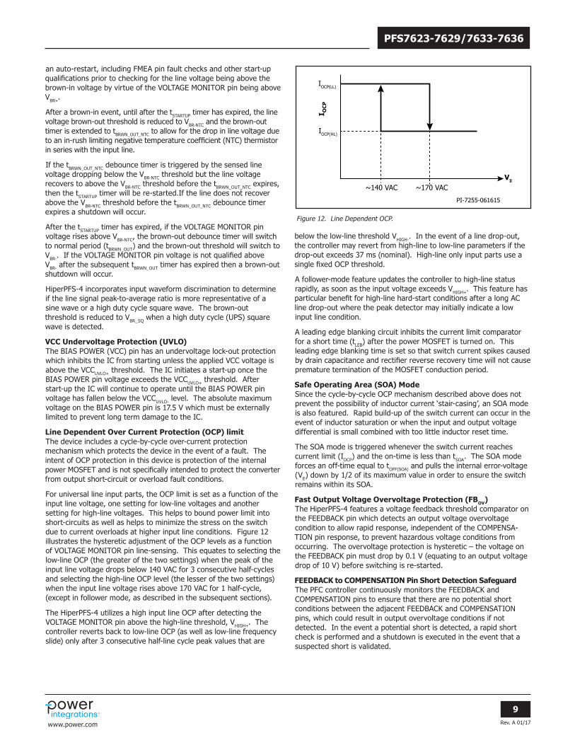
Line Dependent Over Current Protection (OCP) limitThe device includes a cycle-by-cycle over-current protection mechanism which protects the device in the event of a fault. The intent of OCP protection in this device is protection of the internal power MOSFET and is not specifically intended to protect the converter from output short-circuit or overload fault conditions.
For universal line input parts, the OCP limit is set as a function of theinput line voltage, one setting for low-line voltages and anothersetting for high-line voltages. This helps to bound power limit intoshort-circuits as well as helps to minimize the stress on the switchdue to current overloads at higher input line conditions. Figure 12illustrates the hysteretic adjustment of the OCP levels as a functionof VOLTAGE MONITOR pin line-sensing. This equates to selecting thelow-line OCP (the greater of the two settings) when the peak of theinput line voltage drops below 140 VAC for 3 consecutive half-cyclesand selecting the high-line OCP level (the lesser of the two settings)when the input line voltage rises above 170 VAC for 1 half-cycle,(except in follower mode, as described in the subsequent sections).
The HiperPFS-4 utilizes a high input line OCP after detecting theVOLTAGE MONITOR pin above the high-line threshold, VHIGH+. Thecontroller reverts back to low-line OCP (as well as low-line frequencyslide) only after 3 consecutive half-line cycle peak values that are
PI-7255-061615
I OC
P
~170 VACVIN
~140 VAC
IOCP(LL)
IOCP(HL)
Figure 12. Line Dependent OCP.
below the low-line threshold VHIGH-. In the event of a line drop-out, the controller may revert from high-line to low-line parameters if the drop-out exceeds 37 ms (nominal). High-line only input parts use a single fixed OCP threshold.
A follower-mode feature updates the controller to high-line statusrapidly, as soon as the input voltage exceeds VHIGH+. This feature has particular benefit for high-line hard-start conditions after a long AC line drop-out where the peak detector may initially indicate a lowinput line condition.
A leading edge blanking circuit inhibits the current limit comparatorfor a short time (tLEB) after the power MOSFET is turned on. Thisleading edge blanking time is set so that switch current spikes causedby drain capacitance and rectifier reverse recovery time will not causepremature termination of the MOSFET conduction period.
Safe Operating Area (SOA) Mode Since the cycle-by-cycle OCP mechanism described above does notprevent the possibility of inductor current ‘stair-casing’, an SOA modeis also featured. Rapid build-up of the switch current can occur in theevent of inductor saturation or when the input and output voltagedifferential is small combined with too little inductor reset time.
The SOA mode is triggered whenever the switch current reachescurrent limit (IOCP) and the on-time is less than tSOA. The SOA modeforces an off-time equal to tOFF(SOA) and pulls the internal error-voltage(VE) down by 1/2 of its maximum value in order to ensure the switchremains within its SOA.
Fast Output Voltage Overvoltage Protection (FBOV)The HiperPFS-4 features a voltage feedback threshold comparator onthe FEEDBACK pin which detects an output voltage overvoltagecondition to allow rapid response, independent of the COMPENSA-TION pin response, to prevent hazardous voltage conditions fromoccurring. The overvoltage protection is hysteretic – the voltage onthe FEEDBACK pin must drop by 0.1 V (equating to an output voltagedrop of 10 V) before switching is re-started.
FEEDBACK to COMPENSATION Pin Short Detection SafeguardThe PFC controller continuously monitors the FEEDBACK andCOMPENSATION pins to ensure that there are no potential shortconditions between the adjacent FEEDBACK and COMPENSATIONpins, which could result in output overvoltage conditions if notdetected. In the event a potential short is detected, a rapid shortcheck is performed and a shutdown is executed in the event that asuspected short is validated.
Rev. A 01/17
10
PFS7623-7629/7633-7636
www.power.com
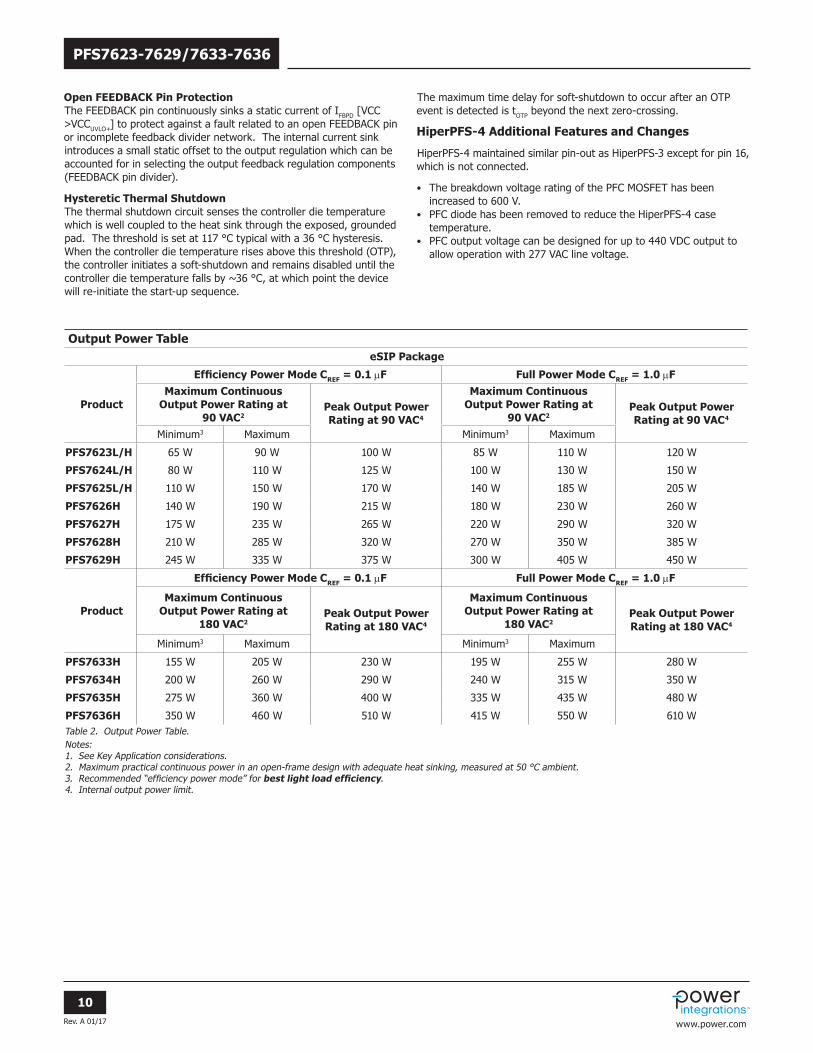
Output Power TableeSIP Package
Product
Efficiency Power Mode CREF = 0.1 mF Full Power Mode CREF = 1.0 mFMaximum Continuous
Output Power Rating at90 VAC2
Peak Output Power Rating at 90 VAC4
Maximum ContinuousOutput Power Rating at
90 VAC2Peak Output Power Rating at 90 VAC4
Minimum3 Maximum Minimum3 Maximum
PFS7623L/H 65 W 90 W 100 W 85 W 110 W 120 W
PFS7624L/H 80 W 110 W 125 W 100 W 130 W 150 W
PFS7625L/H 110 W 150 W 170 W 140 W 185 W 205 W
PFS7626H 140 W 190 W 215 W 180 W 230 W 260 W
PFS7627H 175 W 235 W 265 W 220 W 290 W 320 W
PFS7628H 210 W 285 W 320 W 270 W 350 W 385 W
PFS7629H 245 W 335 W 375 W 300 W 405 W 450 W
Product
Efficiency Power Mode CREF = 0.1 mF Full Power Mode CREF = 1.0 mF
Maximum ContinuousOutput Power Rating at
180 VAC2Peak Output Power Rating at 180 VAC4
Maximum ContinuousOutput Power Rating at
180 VAC2Peak Output Power Rating at 180 VAC4
Minimum3 Maximum Minimum3 Maximum
PFS7633H 155 W 205 W 230 W 195 W 255 W 280 W
PFS7634H 200 W 260 W 290 W 240 W 315 W 350 W
PFS7635H 275 W 360 W 400 W 335 W 435 W 480 W
PFS7636H 350 W 460 W 510 W 415 W 550 W 610 WTable 2. Output Power Table. Notes: 1. See Key Application considerations.2. Maximum practical continuous power in an open-frame design with adequate heat sinking, measured at 50 °C ambient.3. Recommended “efficiency power mode” for best light load efficiency.4. Internal output power limit.
Open FEEDBACK Pin Protection The FEEDBACK pin continuously sinks a static current of IFBPD [VCC >VCCUVLO+] to protect against a fault related to an open FEEDBACK pin or incomplete feedback divider network. The internal current sinkintroduces a small static offset to the output regulation which can beaccounted for in selecting the output feedback regulation components(FEEDBACK pin divider).
Hysteretic Thermal Shutdown The thermal shutdown circuit senses the controller die temperaturewhich is well coupled to the heat sink through the exposed, groundedpad. The threshold is set at 117 °C typical with a 36 °C hysteresis.When the controller die temperature rises above this threshold (OTP),the controller initiates a soft-shutdown and remains disabled until thecontroller die temperature falls by ~36 °C, at which point the devicewill re-initiate the start-up sequence.
The maximum time delay for soft-shutdown to occur after an OTP event is detected is tOTP beyond the next zero-crossing.
HiperPFS-4 Additional Features and Changes
HiperPFS-4 maintained similar pin-out as HiperPFS-3 except for pin 16, which is not connected.
• The breakdown voltage rating of the PFC MOSFET has been increased to 600 V.
• PFC diode has been removed to reduce the HiperPFS-4 case temperature.
• PFC output voltage can be designed for up to 440 VDC output to allow operation with 277 VAC line voltage.
Rev. A 01/17
11
PFS7623-7629/7633-7636
www.power.com
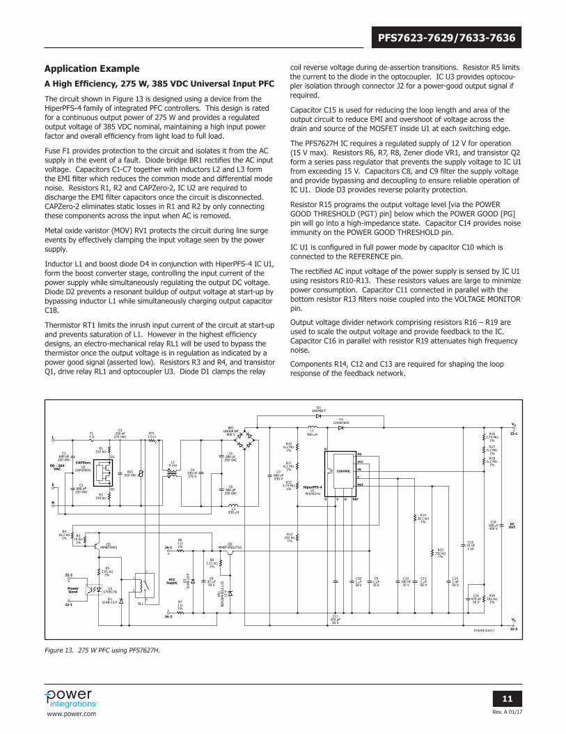
Application Example
A High Efficiency, 275 W, 385 VDC Universal Input PFC
The circuit shown in Figure 13 is designed using a device from theHiperPFS-4 family of integrated PFC controllers. This design is ratedfor a continuous output power of 275 W and provides a regulatedoutput voltage of 385 VDC nominal, maintaining a high input powerfactor and overall efficiency from light load to full load.
Fuse F1 provides protection to the circuit and isolates it from the ACsupply in the event of a fault. Diode bridge BR1 rectifies the AC inputvoltage. Capacitors C1-C7 together with inductors L2 and L3 formthe EMI filter which reduces the common mode and differential modenoise. Resistors R1, R2 and CAPZero-2, IC U2 are required todischarge the EMI filter capacitors once the circuit is disconnected.CAPZero-2 eliminates static losses in R1 and R2 by only connectingthese components across the input when AC is removed.
Metal oxide varistor (MOV) RV1 protects the circuit during line surgeevents by effectively clamping the input voltage seen by the powersupply.
Inductor L1 and boost diode D4 in conjunction with HiperPFS-4 IC U1,form the boost converter stage, controlling the input current of thepower supply while simultaneously regulating the output DC voltage.Diode D2 prevents a resonant buildup of output voltage at start-up bybypassing inductor L1 while simultaneously charging output capacitorC18.
Thermistor RT1 limits the inrush input current of the circuit at start-upand prevents saturation of L1. However in the highest efficiencydesigns, an electro-mechanical relay RL1 will be used to bypass thethermistor once the output voltage is in regulation as indicated by apower good signal (asserted low). Resistors R3 and R4, and transistorQ1, drive relay RL1 and optocoupler U3. Diode D1 clamps the relay
coil reverse voltage during de-assertion transitions. Resistor R5 limits the current to the diode in the optocoupler. IC U3 provides optocou- pler isolation through connector J2 for a power-good output signal if required.
Capacitor C15 is used for reducing the loop length and area of theoutput circuit to reduce EMI and overshoot of voltage across thedrain and source of the MOSFET inside U1 at each switching edge.
The PFS7627H IC requires a regulated supply of 12 V for operation(15 V max). Resistors R6, R7, R8, Zener diode VR1, and transistor Q2form a series pass regulator that prevents the supply voltage to IC U1from exceeding 15 V. Capacitors C8, and C9 filter the supply voltageand provide bypassing and decoupling to ensure reliable operation ofIC U1. Diode D3 provides reverse polarity protection.
Resistor R15 programs the output voltage level [via the POWERGOOD THRESHOLD (PGT) pin] below which the POWER GOOD [PG]pin will go into a high-impedance state. Capacitor C14 provides noiseimmunity on the POWER GOOD THRESHOLD pin.
IC U1 is configured in full power mode by capacitor C10 which isconnected to the REFERENCE pin.
The rectified AC input voltage of the power supply is sensed by IC U1using resistors R10-R13. These resistors values are large to minimizepower consumption. Capacitor C11 connected in parallel with thebottom resistor R13 filters noise coupled into the VOLTAGE MONITORpin.
Output voltage divider network comprising resistors R16 – R19 areused to scale the output voltage and provide feedback to the IC.Capacitor C16 in parallel with resistor R19 attenuates high frequencynoise.
Components R14, C12 and C13 are required for shaping the loopresponse of the feedback network.
L1400 µH
VO
J3-1
J2-2
J4-1
J4-2
RL1J2-1
DCOUT
+
VO
J3-3PI-8054-010317
N
PowerGood
90 - 264VAC
E
L
R1510 kΩ
R61 Ω1%
R310 kΩ1%
R416.2 kΩ
1%
R53.01 kΩ
1%
D1S1AB-13-F
C847 µF50 V
C7680 nF630 V
C91 µF35 V
C101 µF50 V
R1430.1 kΩ
1%
R15332 kΩ
1%
C11470 pF50 V
D3
S1AB
-13-
F
VR1
BZX3
84-B
13,1
1513
V
Q1MMBT4403
3
4
2
1
U3LTV817A
Q2MMBT4401LT1G
R71 Ω1%
R82.21 kΩ
1%
R2510 kΩ
C2680 pF
250 VAC
BR1GBU8K-BP
800 V
L29 mH
C4330 nF275 V
C6680 pF
250 VAC
C5680 pF
250 VAC
C1680 pF
250 VAC
F15 A
RV1520 VAC
VCCSupply
C3330 nF
275 VACRT1
2.5 Ω
D1
CAPZeroU2
CAP200DG
D2
L3330 µH
+
+C141 nF50 V
C18180 µF450 V
R19162 kΩ
1%
R163.74 MΩ
1%R10
6.2 MΩ1%
R116.2 MΩ
1%
R123.74 MΩ
1%
R13162 kΩ
1%
R176.2 MΩ
1%R18
6.2 MΩ1%
C1510 nF1 kV
C131 µF50 V
D21N5408-T
D4LXA06T600
C12100 nF25 V
C16470 pF50 V
tO
S
D
C
PGT
FB
VCC
PG
REFGV
CONTROL
HiperPFS-4U1
PFS7627H
Figure 13. 275 W PFC using PFS7627H.
Rev. A 01/17
12
PFS7623-7629/7633-7636
www.power.com
Design, Assembly, and Layout Considerations
Power TableThe data sheet power table as shown in Table 2 represents the maximum practical continuous output power based on the following conditions:
For the universal input devices (PFS7623L/H – PFS7629H):1. An input voltage range of 90 VAC to 264 VAC.2. Overall efficiency of at least 93% at the lowest operating voltage.3. 385 V nominal output.4. Sufficient heat sinking to keep device temperature ≤100 ºC.
Operation beyond the limits stated above will require de-rating. Operation at elevated temperatures could result in reduced MTBF and performance degradation, e.g. reduced efficiency, reduced power limit, PF, and potential of observing hysteretic brown-out, etc., and is not recommended.
HiperPFS-4 SelectionSelection of the optimum HiperPFS-4 part depends on requiredmaximum output power, PFC efficiency and overall system efficiency(when used with a second stage DC-DC converter), heat sinkingconstraints, system requirements and cost goals. The HiperPFS-4part used in a design can be easily replaced with the next higher orlower part in the power table to optimize performance, improveefficiency or for applications where there are thermal design constraints. Minor adjustments to the inductance value and EMI filtercomponents may be necessary in some designs when the next higheror the next lower HiperPFS-4 part is used in an existing design forperformance optimization.
Every HiperPFS-4 family part has an optimal load level where it offersthe most value. Operating frequency of a part will change dependingon load level. Change of frequency will result in change in peak topeak current ripple in the inductance used. Change in current ripplewill affect input PF and total harmonic distortion of input current.
Input Fuse and Protection CircuitThe input fuse should be rated for a continuous current above theinput current at which the PFC turns-off due to input undervoltage.This voltage is referred to as the brown-out voltage.
The fuse should also have sufficient I2t rating in order to avoidnuisance failures during start-up. At start-up a large current is drawnfrom the input as the output capacitor charges to the peak of theapplied voltage. The charging current is only limited by any inrushlimiting thermistors, impedance of the EMI filter inductors and theforward resistance of the input rectifier diodes. A MOV will typically be required to protect the PFC from line surges. Selection of the MOV rating will depend on the energy level (EN1000-4-5 Class level) which the PFC is required to withstand.
A suitable NTC thermistor should be used on the input side to provideinrush current limiting. Choice of this thermistor should depend onthe inrush current specification for the power supply. NTC thermis-tors may not be placed in any other location in the circuit as they failto limit the stress on the part in the event of line transients and alsofail to limit the inrush current in a predictable manner. The examplein Figure 13 shows the circuit configuration that has the inrushlimiting NTC thermistor on the input side which is bypassed with arelay after PFC start-up. This arrangement ensures that a consistentinrush limiting performance is achieved by the circuit.
Input EMI FilterThe variable switching frequency of the HiperPFS-4 effectively modulates the switching frequency and reduces conducted EMI peaks associated with the harmonics of the fundamental switching frequency.
This is particularly beneficial for the average detection mode used in EMI measurements.
The PFC is a switching converter and will need an EMI filter at theinput in order to meet the requirements of most safety agencystandards for conducted and radiated EMI. Typically a common mode filter with X capacitors connected across the line will provide the required attenuation of high frequency components of input current to an acceptable level. The leakage reactance of the common mode filter inductor and the X capacitors form a low pass filter. In some designs, additional differential filter inductors may have to be used to supplement the differential mode inductance of the common-mode choke.
A filter capacitor with low ESR and high ripple current capabilityshould be connected at the output of the input bridge rectifier. Thiscapacitor reduces the generation of the switching frequency components of the input current ripple and simplifies EMI filter design. Typically, 0.33 mF per 100 W should be used for universal input designs and 0.15 mF per 100 W of output power should be used for 230 VAC only designs.
It is often possible to use a higher value of capacitance after the bridge rectifier and reduce the X capacitance in the EMI filter.
For applications where PF at light load is important, be aware that all capacitors prior to the boost stage are not corrected for PF and thus the larger the capacitor value may degrade PF performance at light load
Regulatory requirements require use of a discharge resistor to beconnected across the input X capacitance on the AC side of thebridge rectifier. This is to ensure that residual charge is dissipatedafter the input voltage is removed when the capacitance is higherthan 0.1 mF. Use of CAPZero-2 integrated circuits from PowerIntegrations, helps eliminate the steady-state losses associated withthe use of discharge resistors connected permanently across the Xcapacitors.
Inductor DesignFor ferrite inductors the optimal design has KP of 0.3 to 0.45. (KP isdefined as the current peak-to-peak value divided by the peak valueat minimum AC voltage and 90° phase angle, full load). KP <0.3(more continuous) tends towards excessive inductor size, while higherKP >0.45 tends towards excessive winding AC resistance losses due to large high-frequency AC currents, especially since most ferriteinductor designs will require >3 winding layers. Flux density atmaximum current limit should be <3900 gauss to prevent coresaturation.
If Sendust core material is used, 90m or 125m material is recommended, because the higher m materials tend to produce greater inductance at lower currents, and thus reduced peak-to-peak inductor currents at lower line phase angles (<45°) which reduces losses and improves PF at lighter loads and higher input voltages. The design target is for H at the peak current (low-line, full-load, 90° line phase angle) to be ~60 A-t/cm. Higher H tends towards excessive core loss, and lower than this increases AC copper losses.
For high performance designs, use of Litz wire is recommended toreduce copper loss due to skin effect and proximity effect. Fortoroidal inductors the numbers of layers should be less than 3 and forbobbin wound inductors, inter layer insulation should be used tominimize inter layer capacitance.
The HiperPFS-4 design spreadsheet simplifies this process and automatically recommends a core size and design for either ferrite or Sendust.
Rev. A 01/17
13
PFS7623-7629/7633-7636
www.power.com
Output DiodeFor a 385 V nominal PFC output voltage, use of a diode with 600 V orhigher PIV rating is recommended. CCM operation with hardswitching demands that diodes with low reverse recovery time andreverse recovery charge should be used. The variable frequencyCCM operation of HiperPFS-4 reduces diode switching losses ascompared to fixed frequency solutions and use of readily availablehigh frequency diodes (such as Qspeed diode family from PowerIntegrations), with soft recovery characteristics that result in areduced EMI. For highly demanding applications such as 80 PLUSGold power supplies, use of Silicon Carbide diodes may be consid-ered. These uses will typically provide further full load improvementin efficiency.
Selected diodes should have a forward continuous current rating of atleast 1.2 A to 1.5 A for every 100 W of output power.
Output CapacitorFor a 385 V nominal PFC output voltage, use of an electrolyticcapacitor with 450 V or higher continuous rating is recommended.The capacitance required is dependent on the acceptable level ofoutput ripple and any hold up time requirements. The equationsbelow provide an easy way to determine the required capacitance inorder to meet the hold-up time requirement and also to meet theoutput ripple require- ments. The higher of the two values would berequired to be used.
The capacitance required for meeting hold-up time requirements is calculated using the equation:
CO PFC output capacitance in farads.PO PFC output power in watts.tHOLD-UP Hold-up time specification for the power supply in seconds.VOUT Lowest nominal output voltage of the PFC in volts.VOUT(MIN) Lowest permissible output voltage of the PFC at the end of hold-up time in volts.
The capacitance required for meeting the low frequency ripple specification is calculated using the equation:
^ h
fL Input frequency in Hz.ΔVO Peak-peak output voltage ripple in volts.ηPFC PFC operating efficiency.IO(MAX) Maximum output current in amps.
The capacitance calculated using the above method should be appropriately increased to account for ageing and tolerances.
Power Supply for the ICA 12 V regulated supply should be used for the HiperPFS-4. If theVCC exceeds 15 V, the HiperPFS-4 may be damaged. In mostapplications a simple series pass linear regulator made using an NPNtransistor and Zener diode is adequate since the HiperPFS-4 onlyrequires approximately ICC(ON) maximum for its operation.
It is recommended that a 1 mF or larger, low ESR ceramic capacitorbe used to decouple the VCC supply. This capacitor should be placeddirectly at the IC pin on the circuit board.
Line-Sense NetworkThe line-sense network connected to the VOLTAGE MONITOR pin provides input voltage information to the HiperPFS-4. A value of 16 MW is chosen in this example design to minimize power consumption in these resistors. Only 1% or better tolerance resistors are recommended.
A decoupling capacitor of 470 pF forming an 80 ms time constant isrequired to be connected in parallel with the bottom resistor from theVOLTAGE MONITOR pin to the GROUND pin of the HiperPFS-4. If theimpedance of the resistor divider is different than that shown in theexample schematic, Figure 13, the decoupling capacitor value mustalso be changed to maintain the 80 ms time constant. This capacitorshould be placed directly at the IC pin on the circuit board.
Feedback NetworkA resistor divider network that provides 3.85 V at the FEEDBACK pin atthe rated output voltage should be used for optimal performance. Itshould be scaled in direct proportion to the VOLTAGE MONITOR pinresistor divider network in order to ensure proper regulation andpower delivery. The HiperPFS-4 controller has been optimized foroperation with an output voltage of 385 VDC. Applications requiringvoltages that deviate from this nominal parameter, thereby requiringa FEEDBACK pin divider ratio other than the recommended 100:1,need to be evaluated for trade-offs of the key target parameters ofthe specific design. E.g.: the VOLTAGE MONITOR pin divider ratioshould be modified to be equivalent to that of the feedback divider inorder to optimize power factor. However, this will have an impact onpower limit, as well as brown-in/brown-out thresholds, etc. Modifica-tion of FEEDBACK and VOLTAGE MONITOR pin resistor divider ratioswithin 2.5% of nominal should not result in dramatically compromisedperformance, but should be thoroughly verified. Changes in excessof this are not recommended. Itemized trade-offs of this type areoutside the scope of this data sheet.
Please refer to DER-547 as a design example with 440 V outputvoltage and 100-300 VAC input voltage. When addressing higherinput voltage designs such as 277 VAC, the output voltage of the PFCneeds to be increased to optimize the performance. If the FEEDBACKpin resistor divider ratio is changed for higher output voltages, ensureFEEDBACK and VOLTAGE pin resistor divider ratios are matched. Alsobe aware that the brown-in/out will also increase as a result ofVOLTAGE pin resistor divider ratio change. Refer to DER-547 reportfor more details.
Voltage de-rating requirements for the power MOSFET, boost diode, and all design choices should be validated with bench tests.
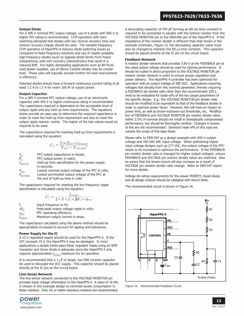
The recommended circuit is shown in Figure 14.
PI-8032-071816
S
D
C
PGT
FB
VCC
PG
REFGV
CONTROL
HiperPFS-4
B+
R2
R4
R5
C3
CREF C2
R1
R3
C1
Figure 14. Recommended Feedback Circuit.

Rev. A 01/17
14
PFS7623-7629/7633-7636
www.power.com
Resistors, R1 to R4 comprise of the main output voltage divider network. The sum of resistors R1, R2 and R3 is the upper divider resistor and the lower feedback resistor is R4. Capacitor C1 is to filter any switching noise from coupling into the FEEDBACK pin. Resistor R5, capacitor C2 and C3 is the loop compensation network required to tailor the loop response to ensure low cross-over frequency and sufficient phase margin. The recommended values for the compo-nents used are as follows:
R1 = 3.74 MWR2 = 6.2 MWR3 = 6.2 MWR5 = 30.1 kWC1 = 470 pF C2 = 1 mFC3 = 100 nF
When the above component values are used, the value of resistor R4 can be calculated using the equation below:
^ hVO Output voltage.VFB(REF) FEEDBACK pin voltage, 3.85 V.
The value of resistor R5 will have to be adjusted in some designs and as a guideline the value from the following calculation can be used:
PO Maximum continuous output power in watts.VO Nominal PFC output voltage in volts.CO PFC output capacitance in farads.
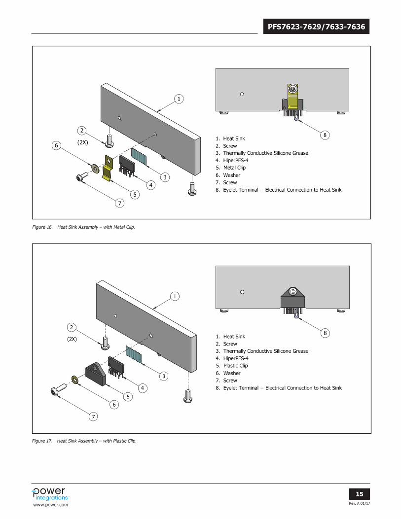
Heat Sinking and Thermal DesignFigures 15, 16, 17 show an example of the recommended assembly for the HiperPFS-4. In this assembly, no insulation pad is required and HiperPFS-4 can be directly connected to the heat sink by mechan-ical clip or adhesive thermal compound.
It is required, on the PCB, that the heat sink is connected to the HiperPFS-4 source terminal in order to reduce EMI and optimize operation.
Figure 15. Heat Sink Assembly – using Thermally Conductive Adhesive.
1
5
3
4
2
(2X) 2. Screw1. Heat Sink
4. HiperPFS-43. Thermally Conductive Adhesive
5. Eyelet Terminal − Electrical Connection to Heat Sink
Rev. A 01/17
15
PFS7623-7629/7633-7636
www.power.com
4
7
5
6
2
3
1
(2X)8
1. Heat Sink
3. Thermally Conductive Silicone Grease
5. Metal Clip6. Washer7. Screw
4. HiperPFS-4
2. Screw
8. Eyelet Terminal − Electrical Connection to Heat Sink
Figure 16. Heat Sink Assembly – with Metal Clip.
1. Heat Sink
3. Thermally Conductive Silicone Grease
5. Plastic Clip6. Washer7. Screw
4. HiperPFS-4
2. Screw
6
7
2
3
4
5
1
(2X)
8. Eyelet Terminal − Electrical Connection to Heat Sink
8
Figure 17. Heat Sink Assembly – with Plastic Clip.
Rev. A 01/17
16
PFS7623-7629/7633-7636
www.power.com
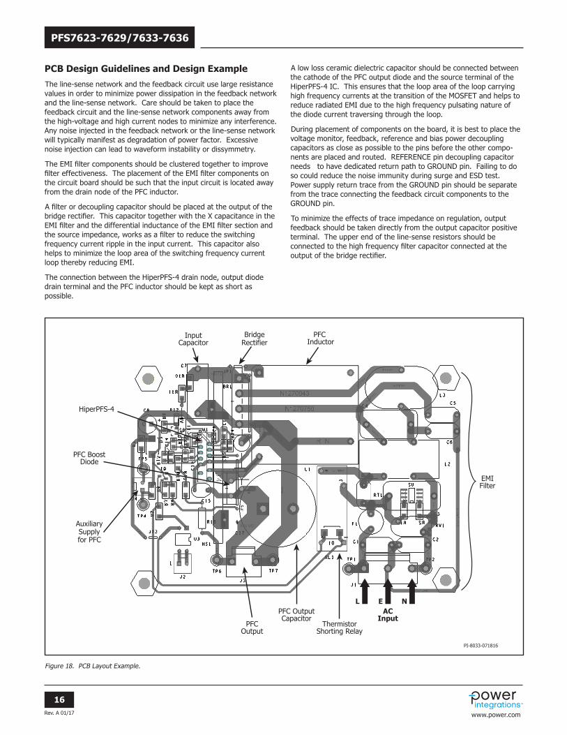
PCB Design Guidelines and Design Example
The line-sense network and the feedback circuit use large resistance values in order to minimize power dissipation in the feedback network and the line-sense network. Care should be taken to place the feedback circuit and the line-sense network components away from the high-voltage and high current nodes to minimize any interference. Any noise injected in the feedback network or the line-sense network will typically manifest as degradation of power factor. Excessive noise injection can lead to waveform instability or dissymmetry.
The EMI filter components should be clustered together to improve filter effectiveness. The placement of the EMI filter components on the circuit board should be such that the input circuit is located away from the drain node of the PFC inductor.
A filter or decoupling capacitor should be placed at the output of the bridge rectifier. This capacitor together with the X capacitance in the EMI filter and the differential inductance of the EMI filter section and the source impedance, works as a filter to reduce the switching frequency current ripple in the input current. This capacitor also helps to minimize the loop area of the switching frequency current loop thereby reducing EMI.
The connection between the HiperPFS-4 drain node, output diode drain terminal and the PFC inductor should be kept as short as possible.
A low loss ceramic dielectric capacitor should be connected between the cathode of the PFC output diode and the source terminal of the HiperPFS-4 IC. This ensures that the loop area of the loop carrying high frequency currents at the transition of the MOSFET and helps to reduce radiated EMI due to the high frequency pulsating nature of the diode current traversing through the loop.
During placement of components on the board, it is best to place the voltage monitor, feedback, reference and bias power decoupling capacitors as close as possible to the pins before the other compo-nents are placed and routed. REFERENCE pin decoupling capacitor needs to have dedicated return path to GROUND pin. Failing to do so could reduce the noise immunity during surge and ESD test. Power supply return trace from the GROUND pin should be separate from the trace connecting the feedback circuit components to the GROUND pin.
To minimize the effects of trace impedance on regulation, output feedback should be taken directly from the output capacitor positive terminal. The upper end of the line-sense resistors should be connected to the high frequency filter capacitor connected at the output of the bridge rectifier.
Figure 18. PCB Layout Example.
EMIFilter
ThermistorShorting Relay
PFCOutput
PFC OutputCapacitor
PFC Inductor
BridgeRectifier
HiperPFS-4
PFC BoostDiode
AuxiliarySupplyfor PFC
InputCapacitor
PI-8033-071816
ACInput
L E N
Rev. A 01/17
17
PFS7623-7629/7633-7636
www.power.com
Quick Design Checklist
As with any power supply design, all HiperPFS-4 family designs should be verified on the bench to make sure that component specifications are not exceeded under worst-case conditions. The following minimum set of tests is strongly recommended:
1. Maximum drain voltage – Verify that peak VDS does not exceed 600 V at lowest input voltage and maximum overload output power. Maximum overload output power occurs when the output is overloaded to a level just above the highest rated load or before the power supply output voltage starts falling out of regulation. Additional external snubbers should be used if this voltage is exceeded. In most designs, addition of a ceramic capacitor in the range of 33 pF and 100 pF connected across the PFC output diode will reduce the maximum drain-source voltage to a level below the BVDSS rating. When measuring drain-source voltage of the MOSFET, a high-voltage probe should be used. When the probe tip is removed, a silver ring in the vicinity of the probe tip can be seen. This ring is at ground potential and the best ground connection point for making noise free measure-
ments. Wrapping stiff wire around the ground ring and then connecting that ground wire into the circuit with the shortest possible wire length, and connecting the probe tip to the point being measured, ensures error free measurement. Probe should be compensated according to probe manufacturer’s guidelines to ensure error-free measurement.
2. Maximum drain current – Drain current can be measured indirectly by monitoring inductor current. A current probe should be inserted between the bridge rectifier and inductor connection. At maximum ambient temperature, minimum input voltage and maximum output load, verify drain current wave- forms at start-up for any signs of inductor saturation. When performing this measurement with Sendust inductor, it is typical to see inductor wave-forms that show exponential increase in current due to permeability drop. This should not be confused with hard saturation.
3. Thermal check – At maximum output power, minimum input voltage and maximum ambient temperature; verify that temperature specifications are not exceeded for the HiperPFS-4, PFC inductor, output diodes and output capacitors. Enough thermal margin should be allowed for the part-to-part variation of the RDS(ON) of HiperPFS-4, as specified in the data sheet. A maximum package temperature of 100 °C is recommended to allow for these variations.4. Input PF should improve with load, if performance is found to
progressively deteriorate with loading, it is a sign of possible noise pick-up by the VOLTAGE MONITOR pin circuit or the feedback divider network and the compensation circuit.
Rev. A 01/17
18
PFS7623-7629/7633-7636
www.power.com
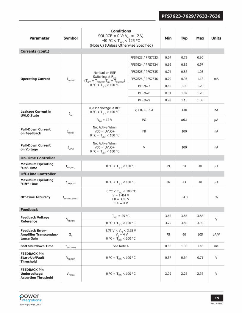
Parameter Symbol
Conditions SOURCE = 0 V; VCC = 12 V,
-40 °C < TJ(C) < 125 °C (Note C) (Unless Otherwise Specified)
Pin Min Typ Max Units
Currents
Undervoltage Current Consumption After Power-Up of Core and Zeners
ICC(UVLO)
VCC < UVLO+(min)V = 1 V, C = 0 V, FB = 3.85 V
0 °C < TJ(C) < 100 °CVCC 140 mA
Standby Current Consumption – No Switching Prior to Brown-In
ICC(STBY)
V = 1 V, C = 0 V, FB = 3.85 V0 °C < TJ(C) < 100 °C
VCC 320 mA
Current Consumption – in Burst Mode, No Switching
ICC(BURST)
FB = 3.85 V, C < VERR_MIN V = 1.414 V
0 °C < TJ(C) < 100 °CVCC 395 470 mA
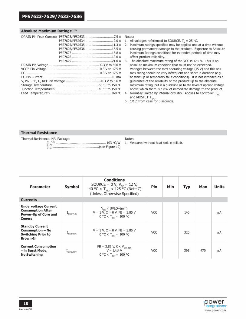
Absolute Maximum Ratings(1,2)
DRAIN Pin Peak Current: PFS7623/PFS7633 .............................7.5 A PFS7624/PFS7634 ............................ 9.0 A PFS7625/PFS7635 ...........................11.3 A PFS7626/PFS7636 ...........................13.5 A PFS7627 .........................................15.8 A PFS7628 .........................................18.0 A PFS7629 .........................................21.0 ADRAIN Pin Voltage ...................................................-0.3 V to 600 V VCC(3) Pin Voltage .................................................... -0.3 V to 17.5 VPG ......................................................................... -0.3 V to 17.5 VPG Pin Current .......................................................................10 mAV, PGT, FB, C, REF Pin Voltage ...................................-0.3 V to 5.6 VStorage Temperature .............................................-65 °C to 150 °C Junction Temperature(4) ...........................................-40 °C to 150 °C Lead Temperature(5) ............................................................. 260 °C
Notes:1. All voltages referenced to SOURCE, TA = 25 °C.2. Maximum ratings specified may be applied one at a time without
causing permanent damage to the product. Exposure to Absolute Maximum Ratings conditions for extended periods of time may affect product reliability.
3. The absolute maximum rating of the VCC is 17.5 V. This is an absolute maximum condition that must not be exceeded. Voltages between the max operating voltage (15 V) and this abs max rating should be very infrequent and short in duration (e.g. at start-up or temporary fault conditions). It is not intended as a guarantee of the reliability of the product up to the absolute maximum rating, but is a guideline as to the level of applied voltage above which there is a risk of immediate damage to the product.
4. Normally limited by internal circuitry. Applies to Controller TJ(C) and MOSFET TJ(M).
5. 1/16” from case for 5 seconds.
Thermal Resistance
Thermal Resistance: H/L Package: (qJA)
(1) ..................................................... 103 °C/W
(qJC) ...............................................(see Figure 19)
Notes: 1. Measured without heat sink in still air.
Rev. A 01/17
19
PFS7623-7629/7633-7636
www.power.com
Parameter Symbol
Conditions SOURCE = 0 V; VCC = 12 V,
-40 °C < TJ(C) < 125 °C (Note C) (Unless Otherwise Specified)
Min Typ Max Units
Currents (cont.)
Operating Current ICC(ON)
No-load on REFSwitching at FMIN
(TOFF = TOFF(MIN) TON = TON(MAX))0 °C < TJ(C) < 100 °C
PFS7623 / PFS7633 0.64 0.75 0.90
mA
PFS7624 / PFS7634 0.69 0.82 0.97
PFS7625 / PFS7635 0.74 0.88 1.05
PFS7626 / PFS7636 0.79 0.93 1.12
PFS7627 0.85 1.00 1.20
PFS7628 0.91 1.07 1.28
PFS7629 0.98 1.15 1.38
Leakage Current in UVLO State Ioz
0 < Pin Voltage < REF0 °C < TJ(C) < 100 °C
V, FB, C, PGT ±10 nA
VPG = 12 V PG ±0.1 mA
Pull-Down Current on Feedback IFB(PD)
Not Active When VCC < UVLO+
0 °C < TJ(C) < 100 °CFB 100 nA
Pull-Down Current on Voltage IV(PD)
Not Active When VCC < UVLO+
0 °C < TJ(C) < 100 °CV 100 nA
On-Time Controller
Maximum Operating “On”-Time tON(MAX) 0 °C < TJ(C) < 100 °C 29 34 40 ms
Off-Time Controller
Maximum Operating “Off”-Time tOFF(MAX) 0 °C < TJ(C) < 100 °C 36 43 48 ms
Off-Time Accuracy tOFF(ACCURACY)
0 °C < TJ(C) < 100 °CV = 1.414 VFB = 3.85 VC > = 4 V
±4.0 %
Feedback
Feedback Voltage Reference VFB(REF)
TJ(C) = 25 °C 3.82 3.85 3.88V
0 °C < TJ(C) < 100 °C 3.75 3.85 3.95
Feedback Error- Amplifier Transconduc-tance Gain
GM
3.75 V < VFB < 3.95 V VC = 4 V
0 °C < TJ(C) < 100 °C75 90 105 µA/V
Soft Shutdown Time tSHUTDWN See Note A 0.86 1.00 1.16 ms
FEEDBACK Pin Start-Up/Fault Threshold
VFB(OFF) 0 °C < TJ(C) < 100 °C 0.57 0.64 0.71 V
FEEDBACK Pin Undervoltage Assertion Threshold
VFB(UV) 0 °C < TJ(C) < 100 °C 2.09 2.25 2.36 V
Rev. A 01/17
20
PFS7623-7629/7633-7636
www.power.com
Parameter Symbol
Conditions SOURCE = 0 V; VCC = 12 V,
-40 °C < TJ(C) < 125 °C (Note C) (Unless Otherwise Specified)
Min Typ Max Units
Feedback (cont.)
FEEDBACK Pin Overvoltage Assertion Threshold
VFB(OV+) 0 °C < TJ(C) < 100 °C 4.00 4.10 4.20 V
FEEDBACK Pin Over- voltage Assertion Relative Threshold
VFB(OV+REL_FB) 0 °C < TJ(C) < 100 °CVFB(REF)
+0.19VFB(REF)
+0.245VFB(REF)
+0.30
FEEDBACK Pin Overvoltage Deassertion Threshold
VFB(OV-) 0 °C < TJ(C) < 100 °C 3.90 4.00 4.10 V
FEEDBACK Pin Over- voltage Deassertion Relative Threshold
VFB(OV-REL_FB) 0 °C < TJ(C) < 100 °CVFB(REF)
+0.11VFB(REF)
+0.16VFB(REF)
+0.21
FEEDBACK Pin Overvoltage Hysteresis
VFB(OVHYST) 0 °C < TJ(C) < 100 °C 0.070 0.085 0.115 V
COMPENSATION Pin PF Enhancer Disable Threshold
VLOW(LOAD+) See Note A 1.1 V
COMPENSATION Pin PF Enhancer Enable Threshold
VLOW(LOAD-) See Note A 1.0 V
COMPENSATION Pin PF Enhancer Threshold Hysteresis
VLOW(LOAD_HYST) See Note A 0.1 V
COMPENSATION Pin Burst Disable Threshold
VERR(MIN+) 0 °C < TJ(C) < 100 °C 0.19 V
COMPENSATION pin Burst Enable Threshold VERR(MIN-) 0 °C < TJ(C) < 100 °C 0.1 V
COMPENSATION Pin Burst Threshold Hysteresis
VERR(HYST) 0 °C < TJ(C) < 100 °C 0.09 V
Line-Sense/Peak Detector
Line-Sense Input Voltage Range VV(RANGE) See Note A 0 4 V
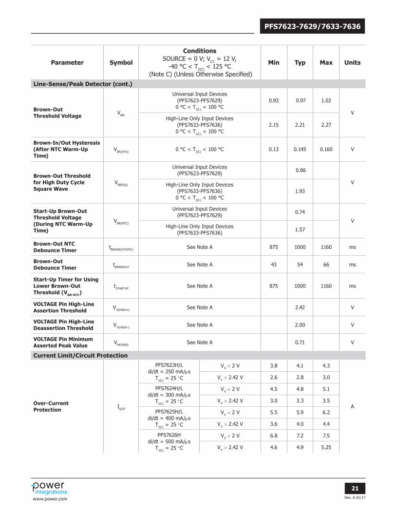
Brown-In Threshold Voltage VBR+
Universal Input Devices (PFS7623-PFS7629)0 °C < TJ(C) < 100 °C
1.08 1.12 1.16
VHigh-Line Only Input Devices
(PFS7633-PFS7636)0 °C < TJ(C) < 100 °C
2.30 2.35 2.42
Rev. A 01/17
21
PFS7623-7629/7633-7636
www.power.com
Parameter Symbol
Conditions SOURCE = 0 V; VCC = 12 V,
-40 °C < TJ(C) < 125 °C (Note C) (Unless Otherwise Specified)
Min Typ Max Units
Line-Sense/Peak Detector (cont.)
Brown-Out Threshold Voltage VBR-
Universal Input Devices (PFS7623-PFS7629)0 °C < TJ(C) < 100 °C
0.93 0.97 1.02
VHigh-Line Only Input Devices
(PFS7633-PFS7636)0 °C < TJ(C) < 100 °C
2.15 2.21 2.27
Brown-In/Out Hysteresis(After NTC Warm-Up Time)
VBR(HYS) 0 °C < TJ(C) < 100 °C 0.13 0.145 0.160 V
Brown-Out Threshold for High Duty Cycle Square Wave
VBR(SQ)
Universal Input Devices (PFS7623-PFS7629)
0.86
VHigh-Line Only Input Devices (PFS7633-PFS7636)0 °C < TJ(C) < 100 °C
1.93
Start-Up Brown-Out Threshold Voltage (During NTC Warm-Up Time)
VBR(NTC)
Universal Input Devices (PFS7623-PFS7629)
0.74
VHigh-Line Only Input Devices
(PFS7633-PFS7636)1.57
Brown-Out NTC Debounce Timer tBRWNOUT(NTC) See Note A 875 1000 1160 ms
Brown-Out Debounce Timer tBRWNOUT See Note A 43 54 66 ms
Start-Up Timer for Using Lower Brown-Out Threshold (VBR-NTC)
tSTARTUP See Note A 875 1000 1160 ms
VOLTAGE Pin High-Line Assertion Threshold VV(HIGH+) See Note A 2.42 V
VOLTAGE Pin High-Line Deassertion Threshold VV(HIGH-) See Note A 2.00 V
VOLTAGE Pin Minimum Asserted Peak Value VPK(MIN) See Note A 0.71 V
Current Limit/Circuit Protection
Over-CurrentProtection IOCP
PFS7623H/Ldi/dt = 250 mA/ms
TJ(C) = 25 °C
VV < 2 V 3.8 4.1 4.3
A
VV > 2.42 V 2.6 2.8 3.0
PFS7624H/Ldi/dt = 300 mA/ms
TJ(C) = 25 °C
VV < 2 V 4.5 4.8 5.1
VV > 2.42 V 3.0 3.3 3.5
PFS7625H/Ldi/dt = 400 mA/ms
TJ(C) = 25 °C
VV < 2 V 5.5 5.9 6.2
VV > 2.42 V 3.6 4.0 4.4
PFS7626Hdi/dt = 500 mA/ms
TJ(C) = 25 °C
VV < 2 V 6.8 7.2 7.5
VV > 2.42 V 4.6 4.9 5.25
Rev. A 01/17
22
PFS7623-7629/7633-7636
www.power.com
Parameter Symbol
Conditions SOURCE = 0 V; VCC = 12 V,
-40 °C < TJ(C) < 125 °C (Note C) (Unless Otherwise Specified)
Min Typ Max Units
Current Limit/Circuit Protection (cont.)
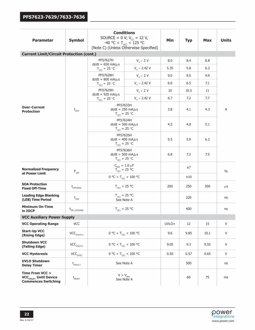
Over-CurrentProtection IOCP
PFS7627Hdi/dt = 650 mA/ms
TJ(C) = 25 °C
VV < 2 V 8.0 8.4 8.8
A
VV > 2.42 V 5.35 5.8 6.2
PFS7628Hdi/dt = 800 mA/ms
TJ(C) = 25 °C
VV < 2 V 9.0 9.5 9.9
VV > 2.42 V 6.0 6.5 7.1
PFS7629Hdi/dt = 920 mA/ms
TJ(C) = 25 °C
VV < 2 V 10 10.5 11
VV > 2.42 V 6.7 7.2 7.7
PFS7633Hdi/dt = 250 mA/ms
TJ(C) = 25 °C3.8 4.1 4.3
PFS7634Hdi/dt = 300 mA/ms
TJ(C) = 25 °C4.5 4.8 5.1
PFS7635Hdi/dt = 400 mA/ms
TJ(C) = 25 °C5.5 5.9 6.2
PFS7636Hdi/dt = 500 mA/ms
TJ(C) = 25 °C6.8 7.2 7.5
Normalized Frequency at Power Limit FLIM
CREF = 1.0 mFTJ(C) = 25 °C
±7%
0 °C < TJ(C) < 100 °C ±10
SOA Protection Fixed Off-Time tOFF(SOA) TJ(C) = 25 °C 200 250 300 ms
Leading Edge Blanking (LEB) Time Period tLEB
TJ(C) = 25 °CSee Note A
220 ns
Minimum On-Time in IOCP tON_OCP(MIN) TJ(C) = 25 °C 400 ns
VCC Auxiliary Power Supply
VCC Operating Range VCC UVLO+ 12 15 V
Start-Up VCC (Rising Edge) VCCUV(LO+) 0 °C < TJ(C) < 100 °C 9.6 9.85 10.1 V
Shutdown VCC(Falling Edge) VCCUV(LO-) 0 °C < TJ(C) < 100 °C 9.05 9.3 9.55 V
VCC Hysteresis VCC(HYS) 0 °C < TJ(C) < 100 °C 0.50 0.57 0.65 V
UVLO Shutdown Delay Timer tUV(LO-) See Note A 500 ns
Time From VCC > VCCUVLO+ Until Device Commences Switching
tRESET
V > VBR+
See Note A60 75 ms
Rev. A 01/17
23
PFS7623-7629/7633-7636
www.power.com
Parameter Symbol
Conditions SOURCE = 0 V; VCC = 12 V,
-40 °C < TJ(C) < 125 °C (Note C) (Unless Otherwise Specified)
Min Typ Max Units
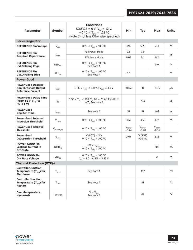
Series Regulator
REFERENCE Pin Voltage VREF 0 °C < TJ(C) < 100 °C 4.95 5.25 5.50 V
REFERENCE Pin Required Capacitance CREF
Full Power Mode 0.8 1.0mF
Efficiency Mode 0.08 0.1 0.2
REFERENCE Pin UVLO Rising Edge REFUV+
0 °C < TJ(C) < 100 °CSee Note A
5.0 V
REFERENCE Pin UVLO Falling Edge REFUV-
0 °C < TJ(C) < 100 °CSee Note A
4.4 V
Power Good
Power Good Deasser-tion Threshold Output Reference Current
IPG(T) 0 °C < TJ(C) < 100 °C; VPGT = 3.0 V -10.65 -10 -9.35 mA
Power Good Delay Time (From FB > VPG+ to PG < 1 V)
tPG
0 °C < TJ(C) < 100 °C; PG = 20 kW Pull-Up to VCC, See Note A
<15 ms
Power Good Deglitch Time tPG(D) See Note A 57 81 108 ms
Power Good Internal Assertion Threshold VPG(+) 0 °C < TJ(C) < 100 °C 3.55 3.65 3.75 V
Power Good Relative Threshold VPG+REL(FB) 0 °C < TJ(C) < 100 °C
VFBREF
-0.24VFBREF
-0.20VFBREF
-0.16
Power Good Deassertion Threshold VPG(-)
V (PGT) = 3 V0 °C < TJ(C) < 100 °C
2.94V (PGT) ±30 mV
3.06 V
POWER GOOD Pin Leakage Current in Off-State
IOZHPG
FB < VPG(-)
0 °C < TJ(C) < 100 °C500 nA
POWER GOOD Pin On-State Voltage VOLPG
0 °C < TJ(C) < 100 °CIPG = 2.0 mA; FB = 3.85 V
2 V
Thermal Protection (OTP)4
Controller Junction Temperature (TJ(C)) for Shutdown
TOTP+ See Note A 117 °C
Controller Junction Temperature (TJ(C)) for Restart
TOTP- See Note A 81 °C
Over-Temperature Hysteresis TOTP(HYST)
V > VBR+ See Note A
36 °C
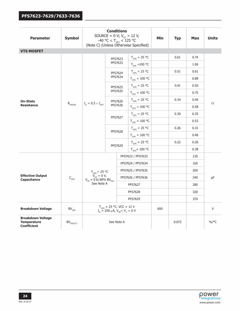
Rev. A 01/17
24
PFS7623-7629/7633-7636
www.power.com
Parameter Symbol
Conditions SOURCE = 0 V; VCC = 12 V,
-40 °C < TJ(C) < 125 °C (Note C) (Unless Otherwise Specified)
Min Typ Max Units
VTS MOSFET
On-State Resistance RDS(ON) ID = 0.5 × IOCP
PFS7623PFS7633
TJ(M) = 25 °C 0.61 0.74
W
TJ(M) =100 °C 1.06
PFS7624PFS7634
TJ(M) = 25 °C 0.51 0.61
TJ(M) = 100 °C 0.88
PFS7625PFS7635
TJ(M) = 25 °C 0.41 0.50
TJ(M) = 100 °C 0.75
PFS7626PFS7636
TJ(M) = 25 °C 0.34 0.40
TJ(M) = 100 °C 0.58
PFS7627TJ(M) = 25 °C 0.30 0.35
TJ(M) = 100 °C 0.53
PFS7628TJ(M) = 25 °C 0.26 0.31
TJ(M) = 100 °C 0.46
PFS7629TJ(M) = 25 °C 0.22 0.26
TJ(M)= 100 °C 0.38
Effective Output Capacitance COSS
TJ(M) = 25 °CVGS = 0 V,
VDS = 0 to 80% BVDSS
See Note A
PFS7623 / PFS7633 135
pF
PFS7624 / PFS7634 165
PFS7625 / PFS7635 200
PFS7626 / PFS7636 240
PFS7627 280
PFS7628 320
PFS7629 370
Breakdown Voltage BVDSS
TJ(M) = 25 °C, VCC = 12 VID = 250 mA, VFB= VV = 0 V
600 V
Breakdown Voltage Temperature Coefficient
BVDSS(TC) See Note A 0.072 %/°C
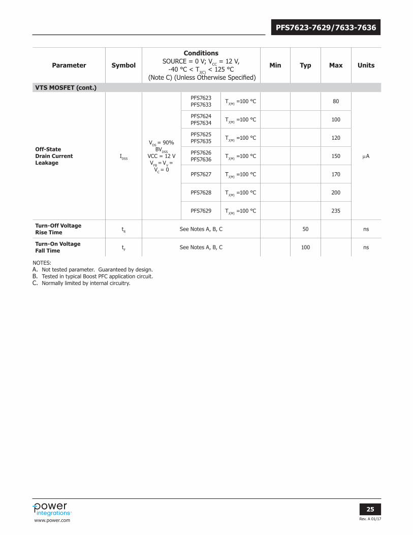
Rev. A 01/17
25
PFS7623-7629/7633-7636
www.power.com
Parameter Symbol
Conditions SOURCE = 0 V; VCC = 12 V,
-40 °C < TJ(C) < 125 °C (Note C) (Unless Otherwise Specified)
Min Typ Max Units
VTS MOSFET (cont.)
Off-State Drain Current Leakage
IDSS
VDS = 90%BVDSS
VCC = 12 V VFB = VV =
VC = 0
PFS7623PFS7633
TJ(M) =100 °C 80
mA
PFS7624PFS7634
TJ(M) =100 °C 100
PFS7625PFS7635
TJ(M) =100 °C 120
PFS7626PFS7636
TJ(M) =100 °C 150
PFS7627 TJ(M) =100 °C 170
PFS7628 TJ(M) =100 °C 200
PFS7629 TJ(M) =100 °C 235
Turn-Off Voltage Rise Time tR See Notes A, B, C 50 ns
Turn-On Voltage Fall Time tF See Notes A, B, C 100 ns
NOTES:A. Not tested parameter. Guaranteed by design.B. Tested in typical Boost PFC application circuit.C. Normally limited by internal circuitry.
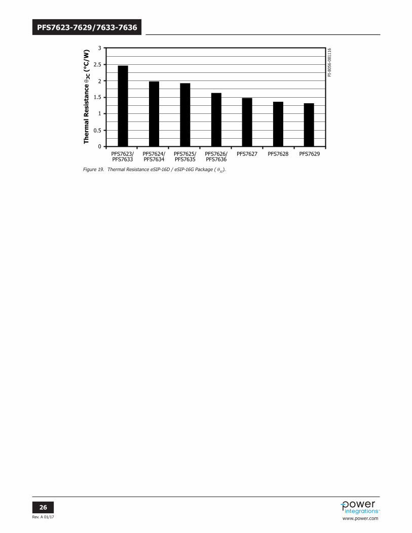
Rev. A 01/17
26
PFS7623-7629/7633-7636
www.power.com
PFS7623/PFS7633
PFS7624/PFS7634
PFS7625/PFS7635
PFS7626/PFS7636
PFS7627 PFS7628 PFS7629
Ther
mal
Res
ista
nce θ J
C (
°C/W
) 3
2.5
2
1.5
1
0.5
0
PI-8
056-
0811
16
Figure 19. Thermal Resistance eSIP-16D / eSIP-16G Package ( qJC).
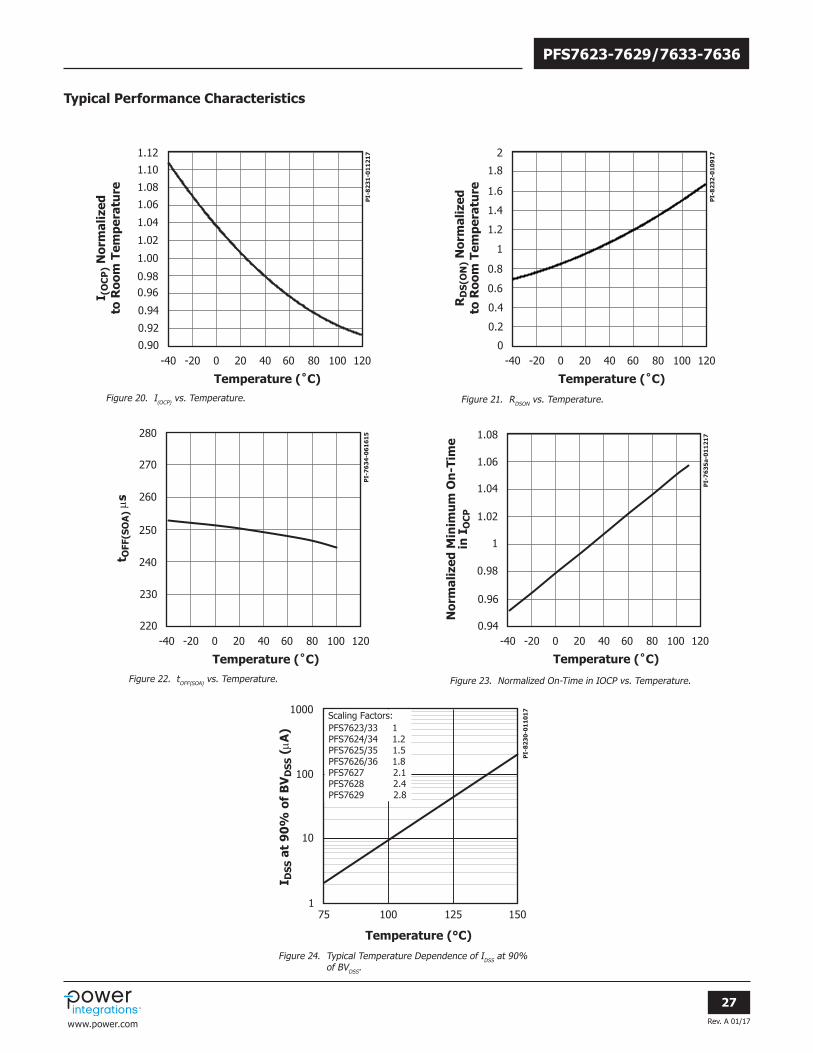
Rev. A 01/17
27
PFS7623-7629/7633-7636
www.power.com
Figure 22. tOFF(SOA) vs. Temperature.
Figure 20. I(OCP) vs. Temperature.
Figure 23. Normalized On-Time in IOCP vs. Temperature.
Figure 21. RDSON vs. Temperature.
Figure 24. Typical Temperature Dependence of IDSS at 90% of BVDSS.
Temperature (˚C)
t OFF
(SO
A) µs
280
270
260
240
230
250
220-40 -20 0 20 6040 10080 120
PI-
76
34
-06
16
15
Temperature (˚C)
Nor
mal
ized
Min
imum
On-
Tim
ein
IO
CP
1.08
1.06
1.04
0.98
1
0.96
1.02
0.94-40 -20 0 20 6040 10080 120
PI-
7635
a-01
1217
75 100 125 1501
10
100
1000
PI-
8230
-011
017
Temperature (°C)
I DSS
at
90%
of
BV
DSS
(µA
) PFS7623/33 1PFS7624/34 1.2PFS7625/35 1.5PFS7626/36 1.8PFS7627 2.1 PFS7628 2.4PFS7629 2.8
Scaling Factors:
Temperature (˚C)
RD
S(O
N)
Nor
mal
ized
to R
oom
Tem
pera
ture
2
1.4
1.6
1.8
1.2
0.6
0.4
0.2
1
0.8
0-40 -20 0 20 6040 10080 120
PI-
8232
-010
917
Typical Performance Characteristics
Temperature (˚C)
I (O
CP
) N
orm
aliz
edto
Roo
m T
empe
ratu
re
1.12
1.08
1.06
1.10
1.04
0.980.96
0.94
0.92
1.02
1.00
0.90-40 -20 0 20 6040 10080 120
PI-
8231
-011
217
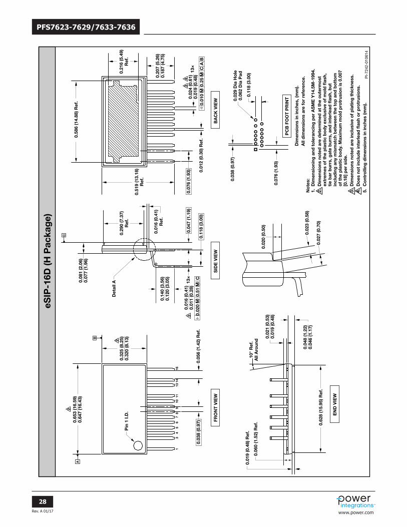
Rev. A 01/17
28
PFS7623-7629/7633-7636
www.power.com
PI-72
42-010
614
No
tes:
1. D
imen
sio
ning
and
to
lera
ncin
g p
er A
SM
E Y
14.5
M-1
994.
2.
Dim
ensi
ons
no
ted
are
det
erm
ined
at
the
out
erm
ost
e
xtre
mes
of
the
pla
stic
bo
dy
excl
usiv
e o
f m
old
flas
h,
tie
bar
bur
rs, g
ate
bur
rs, a
nd in
terl
ead
flas
h, b
ut
inc
lud
ing
any
mis
mat
ch b
etw
een
the
top
and
bo
tto
m
of
the
pla
stic
bo
dy.
Max
imum
mo
ld p
rotr
usio
n is
0.0
07
[
0.18
] p
er s
ide.
3. D
imen
sio
ns n
ote
d a
re in
clus
ive
of
pla
ting
thi
ckne
ss.
4. D
oes
no
t in
clud
e in
terl
ead
flas
h o
r p
rotr
usio
ns.
5. C
ont
rolli
ng d
imen
sio
ns in
inch
es (m
m).
0.62
8 (1
5.95
) Ref
.
0.01
9 (0
.48)
Ref
.
0.06
0 (1
.52)
Ref
.10
° R
ef.
All
Aro
und
0.02
1 (0
.53)
0.01
9 (0
.48)
0.04
8 (1
.22)
0.04
6 (1
.17)
0.02
7 (0
.70)
0.02
3 (0
.58)
0.03
8 (0
.97)
0.07
6 (1
.93)
0.11
8 (3
.00)
0.02
9 D
ia H
ole
0.06
2 D
ia P
ad
0.02
0 (0
.50)
0.01
6 (0
.41)
Ref
.
Det
ail A
0.11
8 (3
.00)
0.14
0 (3
.56)
0.12
0 (3
.05)0.08
1 (2
.06)
0.07
7 (1
.96)
13×
0.01
6 (0
.41)
0.01
1 (0
.28)
0.02
0 M
0.5
1 M
C
3
0.29
0 (7
.37)
Ref
.
0.04
7 (1
.19)
C
0.03
8 (0
.97)
0.05
6 (1
.42)
Ref
.
13
56
78
910
1113
1416
0.65
3 (1
6.59
)0.
647
(16.
43)
2
0.32
5 (8
.25)
0.32
0 (8
.13)2
A
B
Pin
1 I.
D.
0.07
6 (1
.93) 0.
012
(0.3
0) R
ef.
0.20
7 (5
.26)
0.18
7 (4
.75)
13×
0.02
4 (0
.61)
0.01
9 (0
.48)
0.01
0 M
0.2
5 M
C A
B
43
0.51
9 (1
3.18
)R
ef.
FRO
NT
VIE
WS
IDE
VIE
WB
AC
K V
IEW
PC
B F
OO
T P
RIN
T
EN
D V
IEW
eSIP
-16D
(H P
acka
ge)
Dim
ensi
ons
in in
ches
, (m
m).
All
dim
ensi
ons
are
fo
r re
fere
nce.
4
0.58
6 (1
4.88
) Ref
.
0.21
6 (5
.49)
Ref
.
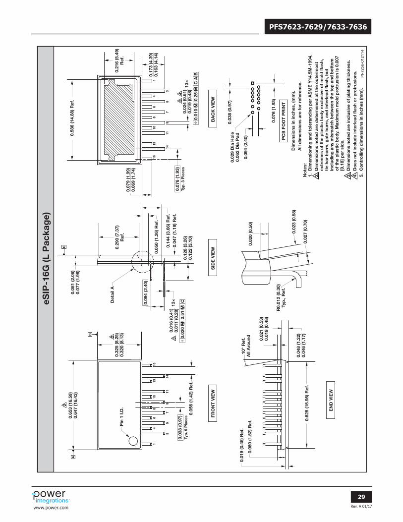
Rev. A 01/17
29
PFS7623-7629/7633-7636
www.power.com
PI-72
56-012
114
No
tes:
1. D
imen
sio
ning
and
to
lera
ncin
g p
er A
SM
E Y
14.5
M-1
994.
2.
Dim
ensi
ons
no
ted
are
det
erm
ined
at
the
out
erm
ost
e
xtre
mes
of
the
pla
stic
bo
dy
excl
usiv
e o
f m
old
flas
h,
tie
bar
bur
rs, g
ate
bur
rs, a
nd in
terl
ead
flas
h, b
ut
inc
lud
ing
any
mis
mat
ch b
etw
een
the
top
and
bo
tto
m
of
the
pla
stic
bo
dy.
Max
imum
mo
ld p
rotr
usio
n is
0.0
07
[
0.18
] p
er s
ide.
3. D
imen
sio
ns n
ote
d a
re in
clus
ive
of
pla
ting
thi
ckne
ss.
4. D
oes
no
t in
clud
e in
terl
ead
flas
h o
r p
rotr
usio
ns.
5. C
ont
rolli
ng d
imen
sio
ns in
inch
es (m
m).
0.03
8 (0
.97)
0.07
6 (1
.93)
0.09
4 (2
.40)
0.02
9 D
ia H
ole
0.06
2 D
ia P
ad
FRO
NT
VIE
WS
IDE
VIE
WB
AC
K V
IEW
PC
B F
OO
T P
RIN
T
EN
D V
IEW
eSIP
-16G
(L P
acka
ge)
0.62
8 (1
5.95
) Ref
.
0.01
9 (0
.48)
Ref
.
0.06
0 (1
.52)
Ref
.10
° R
ef.
All
Aro
und
0.02
1 (0
.53)
0.01
9 (0
.48)
0.04
8 (1
.22)
0.04
6 (1
.17)
Dim
ensi
ons
in in
ches
, (m
m).
All
dim
ensi
ons
are
fo
r re
fere
nce.
0.65
3 (1
6.59
)0.
647
(16.
43)
2
0.32
5 (8
.25)
0.32
0 (8
.13)2
A
B
Pin
1 I.
D.
0.03
8 (0
.97)
Typ
. 9 P
lace
s0.
056
(1.4
2) R
ef.
1
3
1
3
46
810
1316
57
911
14
4
5
6
7
8
9
10
11
13
14
16
C
0.12
8 (3
.26)
0.12
2 (3
.10)
0.08
1 (2
.06)
0.07
7 (1
.96)
Det
ail A
0.09
4 (2
.40)
0.04
7 (1
.19)
Ref
.
0.05
0 (1
.26)
Ref
.
0.14
4 (3
.66)
Ref
.
0.29
0 (7
.37)
Ref
.
13×
0.01
6 (0
.41)
0.01
1 (0
.28)
0.02
0 M
0.5
1 M
C
30.
076
(1.9
3)Ty
p. 3
Pie
ces
0.17
3 (4
.39)
0.16
3 (4
.14)
0.07
9 (1
.99)
0.06
9 (1
.74)
13×
0.02
4 (0
.61)
0.01
9 (0
.48)
0.01
0 M
0.2
5 M
C A
B
43
0.02
7 (0
.70)
0.02
3 (0
.58)
0.02
0 (0
.50)
R0.
012
(0.3
0)Ty
p.,
Ref
.
0.58
6 (1
4.88
) Ref
.
0.21
6 (5
.49)
Ref
.
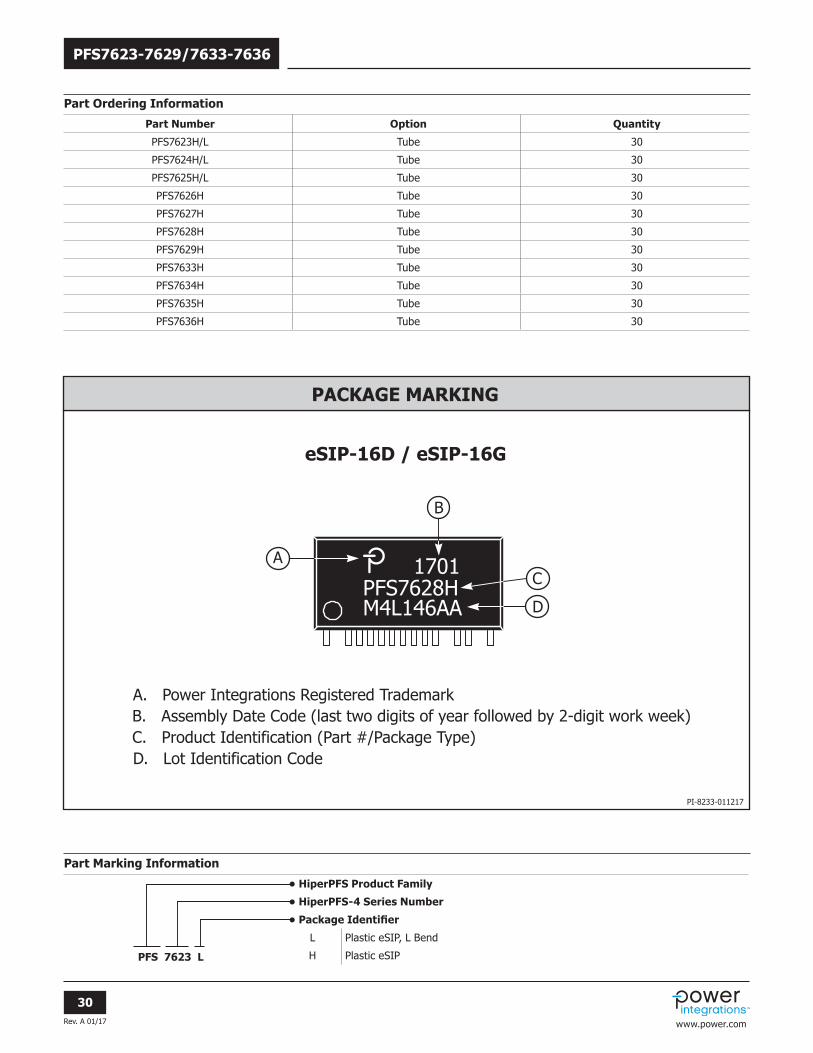
Rev. A 01/17
30
PFS7623-7629/7633-7636
www.power.com
Part Marking Information
• HiperPFS Product Family
• HiperPFS-4 Series Number
• Package Identifier
L Plastic eSIP, L Bend
H Plastic eSIP
Part Ordering Information
Part Number Option Quantity
PFS7623H/L Tube 30
PFS7624H/L Tube 30
PFS7625H/L Tube 30
PFS7626H Tube 30
PFS7627H Tube 30
PFS7628H Tube 30
PFS7629H Tube 30
PFS7633H Tube 30
PFS7634H Tube 30
PFS7635H Tube 30
PFS7636H Tube 30
PFS 7623 L
PI-8233-011217
eSIP-16D / eSIP-16G
A. Power Integrations Registered TrademarkB. Assembly Date Code (last two digits of year followed by 2-digit work week)C. Product Identification (Part #/Package Type)D. Lot Identification Code
PACKAGE MARKING
1701PFS7628HM4L146AA
A
B
D
C
Revision Notes Date
A Code A. 01/17
For the latest updates, visit our website: www.power.comPower Integrations reserves the right to make changes to its products at any time to improve reliability or manufacturability. Power Integrations does not assume any liability arising from the use of any device or circuit described herein. POWER INTEGRATIONS MAKES NO WARRANTY HEREIN AND SPECIFICALLY DISCLAIMS ALL WARRANTIES INCLUDING, WITHOUT LIMITATION, THE IMPLIED WARRANTIES OF MERCHANTABILITY, FITNESS FOR A PARTICULAR PURPOSE, AND NON-INFRINGEMENT OF THIRD PARTY RIGHTS.
Patent InformationThe products and applications illustrated herein (including transformer construction and circuits external to the products) may be covered by one or more U.S. and foreign patents, or potentially by pending U.S. and foreign patent applications assigned to Power Integrations. A complete list of Power Integrations patents may be found at www.power.com. Power Integrations grants its customers a license under certain patent rights as set forth at http://www.power.com/ip.htm.
Life Support PolicyPOWER INTEGRATIONS PRODUCTS ARE NOT AUTHORIZED FOR USE AS CRITICAL COMPONENTS IN LIFE SUPPORT DEVICES OR SYSTEMS WITHOUT THE EXPRESS WRITTEN APPROVAL OF THE PRESIDENT OF POWER INTEGRATIONS. As used herein:
1. A Life support device or system is one which, (i) is intended for surgical implant into the body, or (ii) supports or sustains life, and (iii) whose failure to perform, when properly used in accordance with instructions for use, can be reasonably expected to result in significant injury or death to the user.
2. A critical component is any component of a life support device or system whose failure to perform can be reasonably expected to cause the failure of the life support device or system, or to affect its safety or effectiveness.
The PI logo, TOPSwitch, TinySwitch, SENZero, SCALE-iDriver, Qspeed, PeakSwitch, LYTSwitch, LinkZero, LinkSwitch, InnoSwitch, HiperTFS, HiperPFS, HiperLCS, DPA-Switch, CAPZero, Clampless, EcoSmart, E-Shield, Filterfuse, FluxLink, StakFET, PI Expert and PI FACTS are trademarks of Power Integrations, Inc. Other trademarks are property of their respective companies. ©2017, Power Integrations, Inc.
World Headquarters5245 Hellyer AvenueSan Jose, CA 95138, USAMain: +1-408-414-9200Customer Service:Phone: +1-408-414-9665Fax: +1-408-414-9765e-mail: [email protected]
China (Shanghai)Rm 2410, Charity Plaza, No. 88North Caoxi RoadShanghai, PRC 200030Phone: +86-21-6354-6323Fax: +86-21-6354-6325e-mail: [email protected]
China (Shenzhen)17/F, Hivac Building, No. 2, Keji South 8th Road, Nanshan District, Shenzhen, China, 518057Phone: +86-755-8672-8689Fax: +86-755-8672-8690e-mail: [email protected]
GermanyLindwurmstrasse 11480337 Munich,GermanyPhone: +49-895-527-39110Fax: +49-895-527-39200e-mail: [email protected]
GermanyHellwegForum 159469 EnseGermany Tel: +49-2938-64-39990e-mail: igbt-driver.sales@ power.com
India#1, 14th Main RoadVasanthanagarBangalore-560052 IndiaPhone: +91-80-4113-8020Fax: +91-80-4113-8023e-mail: [email protected]
ItalyVia Milanese 20, 3rd. Fl.,20099 Sesto San Giovanni (MI) ItalyPhone: +39-024-550-8701Fax: +39-028-928-6009e-mail: [email protected]
JapanKosei Dai-3 Bldg. 2-12-11, Shin-Yokohama, Kohoku-ku Yokohama-shi, Kanagawa 222-0033 JapanPhone: +81-45-471-1021Fax: +81-45-471-3717e-mail: [email protected]
KoreaRM 602, 6FLKorea City Air Terminal B/D, 159-6Samsung-Dong, Kangnam-Gu,Seoul, 135-728, KoreaPhone: +82-2-2016-6610Fax: +82-2-2016-6630e-mail: [email protected]
Singapore51 Newton Road#19-01/05 Goldhill PlazaSingapore, 308900Phone: +65-6358-2160Fax: +65-6358-2015e-mail: [email protected]
Taiwan5F, No. 318, Nei Hu Rd., Sec. 1,Nei Hu Dist.Taipei 11493, Taiwan R.O.C.Phone: +886-2-2659-4570Fax: +886-2-2659-4550e-mail: [email protected]
UKBuilding 5, Suite 21The Westbrook CentreMilton RoadCambridge CB4 1YGPhone: +44 (0) 7823-557484e-mail: [email protected]
Power Integrations Worldwide Sales Support Locations