Embed Size (px)
Citation preview
Low-Power High-Resolution CMOS SC ΔΣ ADCs Intro ΔΣMs Circuits Design Results Conclusions 1/72
Low-Power High-Resolution CMOSSwitched-Capacitor Delta-SigmaAnalog-to-Digital Converters
for Sensor Applications
Stepan Sutula1
Directors: Dr. Michele Dei1, Dr. Carles Ferrer Ramis1,2, Dr. Francesc Serra Graells1,2
1Integrated Circuits and Systems (ICAS)Institut de Microelectrònica de Barcelona, IMB-CNM(CSIC)
2Dept. of Microelectronics and Electronic Systems (DEMISE)Universitat Autònoma de Barcelona (UAB)
November 5, 2015
Stepan Sutula
Low-Power High-Resolution CMOS SC ΔΣ ADCs Intro ΔΣMs Circuits Design Results Conclusions 1/72
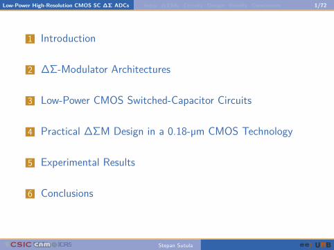
1 Introduction
2 ΔΣ-Modulator Architectures
3 Low-Power CMOS Switched-Capacitor Circuits
4 Practical ΔΣM Design in a 0.18-µm CMOS Technology
5 Experimental Results
6 Conclusions
Stepan Sutula
Low-Power High-Resolution CMOS SC ΔΣ ADCs Intro ΔΣMs Circuits Design Results Conclusions 1/72
1 Introduction
2 ΔΣ-Modulator Architectures
3 Low-Power CMOS Switched-Capacitor Circuits
4 Practical ΔΣM Design in a 0.18-µm CMOS Technology
5 Experimental Results
6 Conclusions
Stepan Sutula
Low-Power High-Resolution CMOS SC ΔΣ ADCs Intro ΔΣMs Circuits Design Results Conclusions 2/72
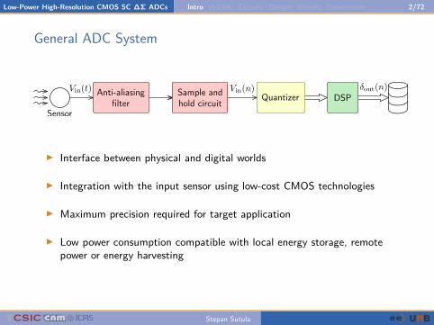
General ADC System
I Interface between physical and digital worlds
I Integration with the input sensor using low-cost CMOS technologies
I Maximum precision required for target application
I Low power consumption compatible with local energy storage, remotepower or energy harvesting
Stepan Sutula
Low-Power High-Resolution CMOS SC ΔΣ ADCs Intro ΔΣMs Circuits Design Results Conclusions 3/72
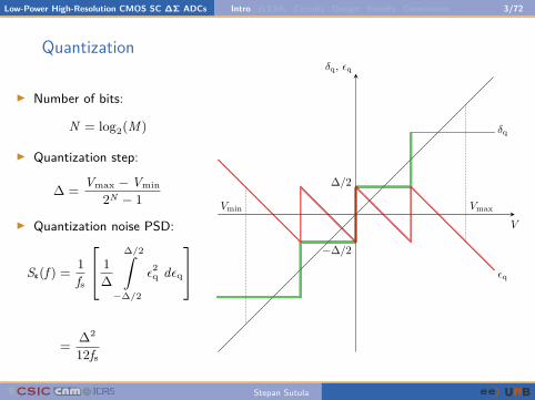
Quantization
I Number of bits:
N = log2(M )
I Quantization step:
∆ = Vmax −Vmin
2N − 1
I Quantization noise PSD:
Sε(f ) = 1fs
1
∆
∆/2∫
−∆/2
ε2q dεq
= ∆2
12fs
Stepan Sutula
Low-Power High-Resolution CMOS SC ΔΣ ADCs Intro ΔΣMs Circuits Design Results Conclusions 4/72
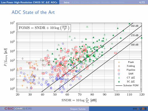
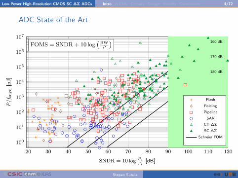
ADC State of the Art
20 30 40 50 60 70 80 90 100 110 120100
101
102
103
104
105
106
107
FOMS = SNDR + 10 log( BW
P
) 160 dB
170 dB
180 dB
SNDR = 10 log PsPε [dB]
P/f sn
yq[p
J]
FlashFoldingPipeline
SARCT ΔΣSC ΔΣ
Schreier FOM
Stepan Sutula
Low-Power High-Resolution CMOS SC ΔΣ ADCs Intro ΔΣMs Circuits Design Results Conclusions 4/72
ADC State of the Art
20 30 40 50 60 70 80 90 100 110 120100
101
102
103
104
105
106
107
FOMS = SNDR + 10 log( BW
P
) 160 dB
170 dB
180 dB
SNDR = 10 log PsPε [dB]
P/f sn
yq[p
J]
FlashFoldingPipeline
SARCT ΔΣSC ΔΣ
Schreier FOM
Stepan Sutula
Low-Power High-Resolution CMOS SC ΔΣ ADCs Intro ΔΣMs Circuits Design Results Conclusions 5/72
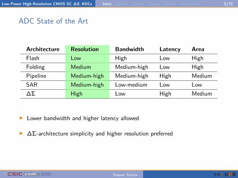
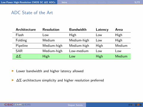
ADC State of the Art
Architecture Resolution Bandwidth Latency AreaFlash Low High Low HighFolding Medium Medium-high Low HighPipeline Medium-high Medium-high High MediumSAR Medium-high Low-medium Low LowΔΣ High Low High Medium
I Lower bandwidth and higher latency allowed
I ΔΣ-architecture simplicity and higher resolution preferred
Stepan Sutula
Low-Power High-Resolution CMOS SC ΔΣ ADCs Intro ΔΣMs Circuits Design Results Conclusions 5/72
ADC State of the Art
Architecture Resolution Bandwidth Latency AreaFlash Low High Low HighFolding Medium Medium-high Low HighPipeline Medium-high Medium-high High MediumSAR Medium-high Low-medium Low LowΔΣ High Low High Medium
I Lower bandwidth and higher latency allowed
I ΔΣ-architecture simplicity and higher resolution preferred
Stepan Sutula
Low-Power High-Resolution CMOS SC ΔΣ ADCs Intro ΔΣMs Circuits Design Results Conclusions 6/72
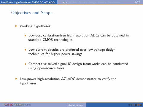
Objectives and Scope
I Working hypotheses:
• Low-cost calibration-free high-resolution ADCs can be obtained instandard CMOS technologies
• Low-current circuits are preferred over low-voltage designtechniques for higher power savings
• Competitive mixed-signal IC design frameworks can be conductedusing open-source tools
I Low-power high-resolution ΔΣ-ADC demonstrator to verify thehypotheses
Stepan Sutula
Low-Power High-Resolution CMOS SC ΔΣ ADCs Intro ΔΣMs Circuits Design Results Conclusions 6/72
1 Introduction
2 ΔΣ-Modulator Architectures
3 Low-Power CMOS Switched-Capacitor Circuits
4 Practical ΔΣM Design in a 0.18-µm CMOS Technology
5 Experimental Results
6 Conclusions
Stepan Sutula
Low-Power High-Resolution CMOS SC ΔΣ ADCs Intro ΔΣMs Circuits Design Results Conclusions 7/72
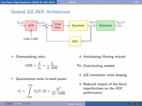
General ΔΣ-ADC Architecture
I Oversampling ratio:
OSR = fsfN
= fs2 · BW
I Quantization-noise in-band power:
Pε =BW∫
−BW
Sε(f ) df = ∆2
12 ·OSR
I Antialiasing filtering relaxed
J I Overclocking needed
I ΔΣ-modulator noise shapingI Reduced impact of the block
imperfections on the ADCperformance
Stepan Sutula
Low-Power High-Resolution CMOS SC ΔΣ ADCs Intro ΔΣMs Circuits Design Results Conclusions 8/72
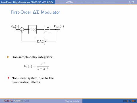
First-Order ΔΣ Modulator
I One-sample-delay integrator:
H1(z) = z−1
1− z−1
J Non-linear system due to thequantization effects
Stepan Sutula
Low-Power High-Resolution CMOS SC ΔΣ ADCs Intro ΔΣMs Circuits Design Results Conclusions 8/72
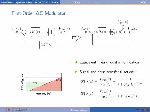
First-Order ΔΣ Modulator
I Equivalent linear-model simplification
I Signal and noise transfer functions:
STF(z) = Vout(z)Vin(z) = 1
1 + (aqH1(z))−1
NTF(z) = Vout(z)Vqn(z) = 1
1 + aqH1(z)
Stepan Sutula
Low-Power High-Resolution CMOS SC ΔΣ ADCs Intro ΔΣMs Circuits Design Results Conclusions 9/72
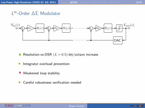
Lth-Order ΔΣ ModulatorI Resolution-vs-OSR (L + 0.5)-bit/octave increase
I Integrator overload prevention
J Weakened loop stability
I Careful robustness verification needed
Stepan Sutula
Low-Power High-Resolution CMOS SC ΔΣ ADCs Intro ΔΣMs Circuits Design Results Conclusions 10/72
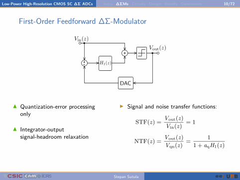
First-Order Feedforward ΔΣ-ModulatorI Quantization-error processing
only
I Integrator-outputsignal-headroom relaxation
I Signal and noise transfer functions:
STF(z) = Vout(z)Vin(z) = 1
NTF(z) = Vout(z)Vqn(z) = 1
1 + aqH1(z)
Stepan Sutula
Low-Power High-Resolution CMOS SC ΔΣ ADCs Intro ΔΣMs Circuits Design Results Conclusions 11/72
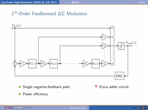
Lth-Order Feedforward ΔΣ ModulatorI Single negative-feedback path
I Power efficiencyJ Extra adder circuit
Stepan Sutula
Low-Power High-Resolution CMOS SC ΔΣ ADCs Intro ΔΣMs Circuits Design Results Conclusions 12/72
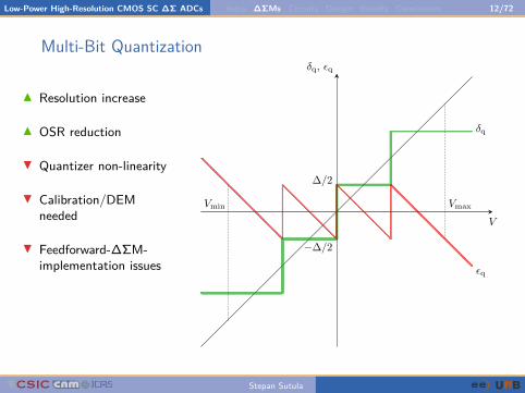
Multi-Bit QuantizationI Resolution increase
I OSR reduction
J Quantizer non-linearity
J Calibration/DEMneeded
J Feedforward-ΔΣM-implementation issues
Stepan Sutula
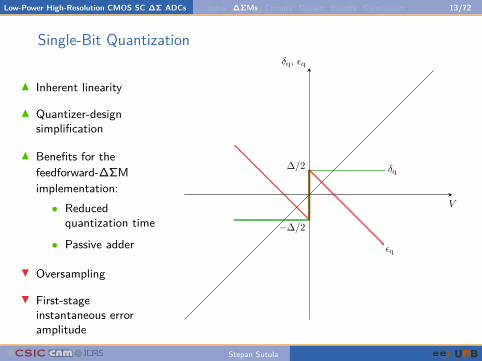
Low-Power High-Resolution CMOS SC ΔΣ ADCs Intro ΔΣMs Circuits Design Results Conclusions 13/72
Single-Bit QuantizationI Inherent linearity
I Quantizer-designsimplification
I Benefits for thefeedforward-ΔΣMimplementation:• Reduced
quantization time• Passive adder
J Oversampling
J First-stageinstantaneous erroramplitude
Stepan Sutula
Low-Power High-Resolution CMOS SC ΔΣ ADCs Intro ΔΣMs Circuits Design Results Conclusions 14/72
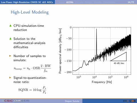
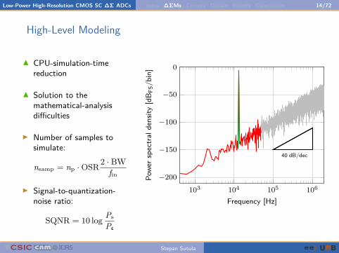
High-Level ModelingI CPU-simulation-time
reduction
I Solution to themathematical-analysisdifficulties
I Number of samples tosimulate:
nsamp = np ·OSR 2 · BWfin
I Signal-to-quantization-noise ratio:
SQNR = 10 log Ps
Pε
103 104 105 106
−200
−150
−100
−50
0
40 dB/dec
Frequency [Hz]
Powe
rspe
ctra
lden
sity
[dB F
S/bi
n]
Stepan Sutula
Low-Power High-Resolution CMOS SC ΔΣ ADCs Intro ΔΣMs Circuits Design Results Conclusions 14/72
High-Level ModelingI CPU-simulation-time
reduction
I Solution to themathematical-analysisdifficulties
I Number of samples tosimulate:
nsamp = np ·OSR 2 · BWfin
I Signal-to-quantization-noise ratio:
SQNR = 10 log Ps
Pε
103 104 105 106
−200
−150
−100
−50
0
40 dB/dec
Frequency [Hz]
Powe
rspe
ctra
lden
sity
[dB F
S/bi
n]
Stepan Sutula
Low-Power High-Resolution CMOS SC ΔΣ ADCs Intro ΔΣMs Circuits Design Results Conclusions 15/72
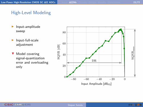
High-Level Modeling
I Input-amplitudesweep
I Input-full-scaleadjustment
J Model coveringsignal-quantizationerror and overloadingonly
Stepan Sutula
Low-Power High-Resolution CMOS SC ΔΣ ADCs Intro ΔΣMs Circuits Design Results Conclusions 16/72
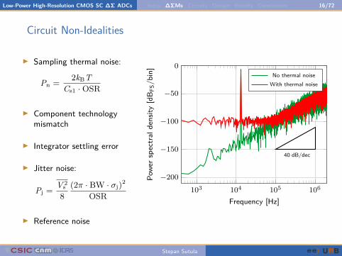
Circuit Non-Idealities
I Sampling thermal noise:
Pn = 2kBTCs1 ·OSR
I Component technologymismatch
I Integrator settling error
I Jitter noise:
Pj = V 2s
8(2π · BW · σj)2
OSR
I Reference noise
103 104 105 106
−200
−150
−100
−50
0
40 dB/dec
Frequency [Hz]
Powe
rspe
ctra
lden
sity
[dB F
S/bi
n] No thermal noiseWith thermal noise
Stepan Sutula
Low-Power High-Resolution CMOS SC ΔΣ ADCs Intro ΔΣMs Circuits Design Results Conclusions 17/72
Demonstrator Target Specifications
I 50-kHz bandwidth
I 16-bit resolution
I Standard CMOS technology
I No supply bootstrapping
I No analog calibration
I No digital compensation
Stepan Sutula
Low-Power High-Resolution CMOS SC ΔΣ ADCs Intro ΔΣMs Circuits Design Results Conclusions 17/72
1 Introduction
2 ΔΣ-Modulator Architectures
3 Low-Power CMOS Switched-Capacitor Circuits
4 Practical ΔΣM Design in a 0.18-µm CMOS Technology
5 Experimental Results
6 Conclusions
Stepan Sutula
Low-Power High-Resolution CMOS SC ΔΣ ADCs Intro ΔΣMs Circuits Design Results Conclusions 18/72
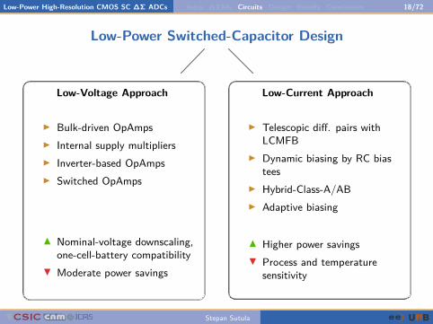
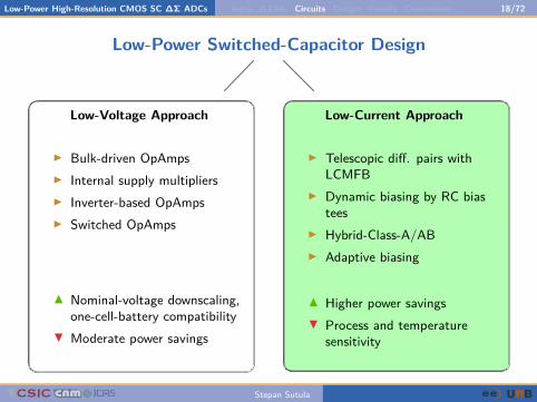
Low-Power Switched-Capacitor Design
Low-Voltage Approach
I Bulk-driven OpAmpsI Internal supply multipliersI Inverter-based OpAmpsI Switched OpAmps
I Nominal-voltage downscaling,one-cell-battery compatibility
J Moderate power savings
Low-Current Approach
I Telescopic diff. pairs withLCMFB
I Dynamic biasing by RC biastees
I Hybrid-Class-A/ABI Adaptive biasing
I Higher power savingsJ Process and temperature
sensitivity
Stepan Sutula
Low-Power High-Resolution CMOS SC ΔΣ ADCs Intro ΔΣMs Circuits Design Results Conclusions 18/72
Low-Power Switched-Capacitor Design
Low-Voltage Approach
I Bulk-driven OpAmpsI Internal supply multipliersI Inverter-based OpAmpsI Switched OpAmps
I Nominal-voltage downscaling,one-cell-battery compatibility
J Moderate power savings
Low-Current Approach
I Telescopic diff. pairs withLCMFB
I Dynamic biasing by RC biastees
I Hybrid-Class-A/ABI Adaptive biasing
I Higher power savingsJ Process and temperature
sensitivity
Stepan Sutula
Low-Power High-Resolution CMOS SC ΔΣ ADCs Intro ΔΣMs Circuits Design Results Conclusions 19/72
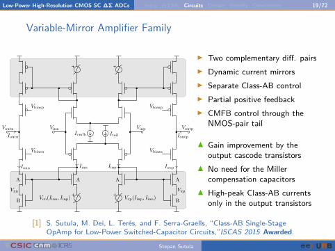
Variable-Mirror Amplifier Family
I Two complementary diff. pairsI Dynamic current mirrorsI Separate Class-AB controlI Partial positive feedbackI CMFB control through the
NMOS-pair tail
I Gain improvement by theoutput cascode transistors
I No need for the Millercompensation capacitors
I High-peak Class-AB currentsonly in the output transistors
[1] S. Sutula, M. Dei, L. Terés, and F. Serra-Graells, “Class-AB Single-StageOpAmp for Low-Power Switched-Capacitor Circuits,”ISCAS 2015 Awarded.
Stepan Sutula
Low-Power High-Resolution CMOS SC ΔΣ ADCs Intro ΔΣMs Circuits Design Results Conclusions 20/72
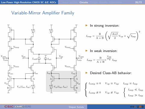
Variable-Mirror Amplifier Family
I In strong inversion:
Ionp =B
A + B
(√Anβ2
Vcp +√
Iinp
)2
I In weak inversion:
Ionp =B
A + Be
VcpUT Iinp
I Desired Class-AB behavior:
Ioutp ≡ 0 Vcp ≡ Vxp Ionp ≡ Iinp
Ioutp 6≡ 0 Vcp 6≡ Vxp
{Ionp � Iinp
Ionp � Iinp
Stepan Sutula
Low-Power High-Resolution CMOS SC ΔΣ ADCs Intro ΔΣMs Circuits Design Results Conclusions 21/72
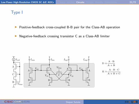
Type I
I Positive-feedback cross-coupled B-B pair for the Class-AB operation
I Negative-feedback crossing transistor C as a Class-AB limiter
D.=
A · BA + B
E.=
A · B · CA + B + C
Stepan Sutula
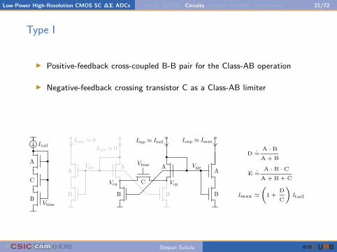
Low-Power High-Resolution CMOS SC ΔΣ ADCs Intro ΔΣMs Circuits Design Results Conclusions 21/72
Type I
I Positive-feedback cross-coupled B-B pair for the Class-AB operation
I Negative-feedback crossing transistor C as a Class-AB limiter
D.=
A · BA + B
E.=
A · B · CA + B + C
Imax '(1 +
DC
)Itail
Stepan Sutula
Low-Power High-Resolution CMOS SC ΔΣ ADCs Intro ΔΣMs Circuits Design Results Conclusions 22/72
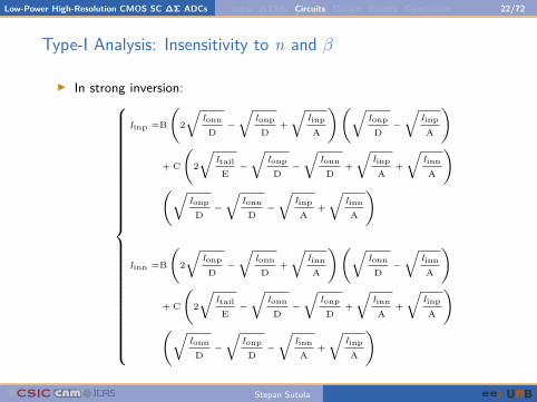
Type-I Analysis: Insensitivity to n and β
I In strong inversion:
Iinp =B
(2
√IonnD−
√IonpD
+
√IinpA
)(√IonpD−
√IinpA
)
+ C
(2
√ItailE−
√IonpD−
√IonnD
+
√IinpA
+
√IinnA
)
(√IonpD−
√IonnD−
√IinpA
+
√IinnA
)
Iinn =B
(2
√IonpD−
√IonnD
+
√IinnA
)(√IonnD−
√IinnA
)
+ C
(2
√ItailE−
√IonnD−
√IonpD
+
√IinnA
+
√IinpA
)
(√IonnD−
√IonpD−
√IinnA
+
√IinpA
)
Stepan Sutula
Low-Power High-Resolution CMOS SC ΔΣ ADCs Intro ΔΣMs Circuits Design Results Conclusions 23/72
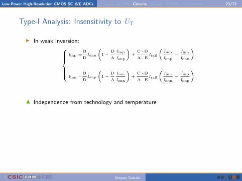
Type-I Analysis: Insensitivity to UT
I In weak inversion:
Iinp =BD
Ionn
(1−
DA
IinpIonp
)+
C · DA · E
Itail
(IinpIonp
−IinnIonn
)
Iinn =BD
Ionp
(1−
DA
IinnIonn
)+
C · DA · E
Itail
(IinnIonn
−IinpIonp
)
I Independence from technology and temperature
Stepan Sutula
Low-Power High-Resolution CMOS SC ΔΣ ADCs Intro ΔΣMs Circuits Design Results Conclusions 24/72
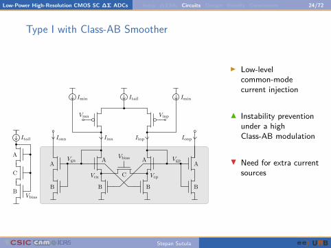
Type I with Class-AB Smoother
I Low-levelcommon-modecurrent injection
I Instability preventionunder a highClass-AB modulation
J Need for extra currentsources
Stepan Sutula
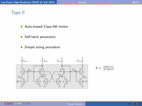
Low-Power High-Resolution CMOS SC ΔΣ ADCs Intro ΔΣMs Circuits Design Results Conclusions 25/72
Type III Auto-biased Class-AB limiter
I Self-latch prevention
I Simple sizing procedure
F .= A(B+C)A+B+C
Stepan Sutula
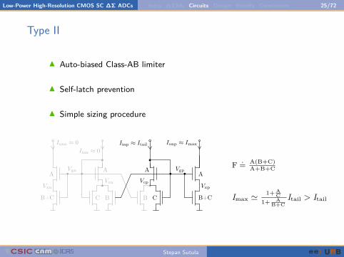
Low-Power High-Resolution CMOS SC ΔΣ ADCs Intro ΔΣMs Circuits Design Results Conclusions 25/72
Type III Auto-biased Class-AB limiter
I Self-latch prevention
I Simple sizing procedure
F .= A(B+C)A+B+C
Imax '1+A
C1+ A
B+CItail > Itail
Stepan Sutula
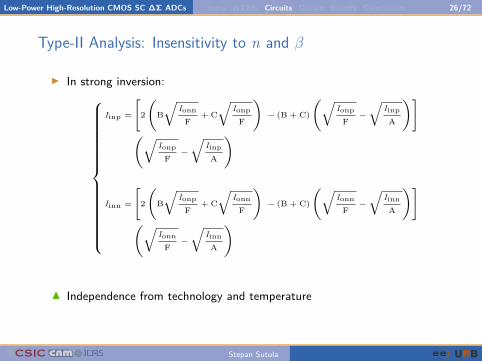
Low-Power High-Resolution CMOS SC ΔΣ ADCs Intro ΔΣMs Circuits Design Results Conclusions 26/72
Type-II Analysis: Insensitivity to n and β
I In strong inversion:
Iinp =
[2
(B
√IonnF
+ C
√IonpF
)− (B + C)
(√IonpF−
√IinpA
)]
(√IonpF−
√IinpA
)
Iinn =
[2
(B
√IonpF
+ C
√IonnF
)− (B + C)
(√IonnF−
√IinnA
)]
(√IonnF−
√IinnA
)
I Independence from technology and temperature
Stepan Sutula

Low-Power High-Resolution CMOS SC ΔΣ ADCs Intro ΔΣMs Circuits Design Results Conclusions 27/72
Type-II Analysis: Insensitivity to UT
I In weak inversion:
Iinp =(BF
Ionn +CF
Ionp
)(1−
FA
IinpIonp
)
Iinn =(BF
Ionp +CF
Ionn
)(1−
FA
IinnIonn
)
I Independence from technology and temperature
Stepan Sutula
Low-Power High-Resolution CMOS SC ΔΣ ADCs Intro ΔΣMs Circuits Design Results Conclusions 28/72
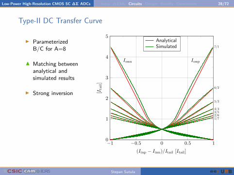
Type-II DC Transfer Curve
I ParameterizedB/C for A=8
I Matching betweenanalytical andsimulated results
I Strong inversion
Stepan Sutula
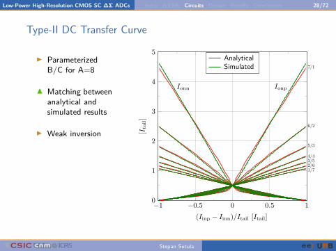
Low-Power High-Resolution CMOS SC ΔΣ ADCs Intro ΔΣMs Circuits Design Results Conclusions 28/72
Type-II DC Transfer Curve
I ParameterizedB/C for A=8
I Matching betweenanalytical andsimulated results
I Weak inversion
Stepan Sutula
Low-Power High-Resolution CMOS SC ΔΣ ADCs Intro ΔΣMs Circuits Design Results Conclusions 29/72
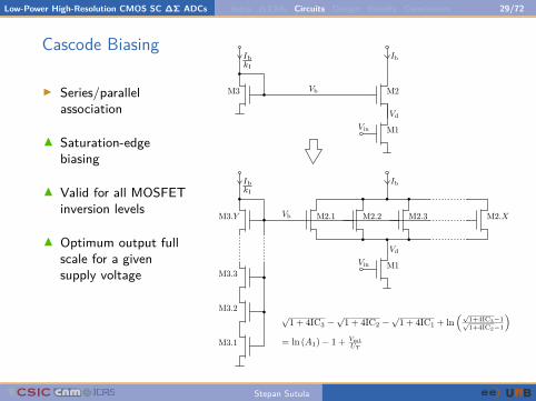
Cascode Biasing
I Series/parallelassociation
I Saturation-edgebiasing
I Valid for all MOSFETinversion levels
I Optimum output fullscale for a givensupply voltage
Stepan Sutula
Low-Power High-Resolution CMOS SC ΔΣ ADCs Intro ΔΣMs Circuits Design Results Conclusions 30/72
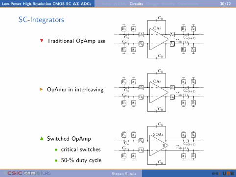
SC-Integrators
J Traditional OpAmp use
I OpAmp in interleaving
I Switched OpAmp• critical switches
• 50-% duty cycle
Stepan Sutula
Low-Power High-Resolution CMOS SC ΔΣ ADCs Intro ΔΣMs Circuits Design Results Conclusions 31/72
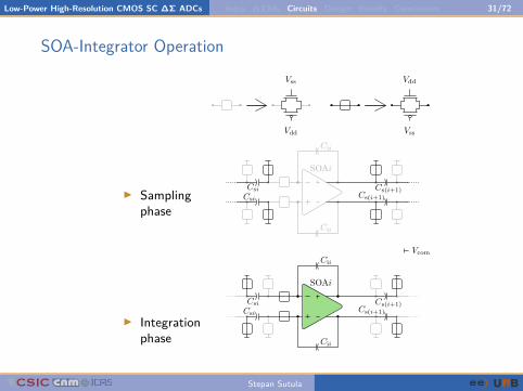
SOA-Integrator Operation
I Samplingphase
I Integrationphase
Stepan Sutula
Low-Power High-Resolution CMOS SC ΔΣ ADCs Intro ΔΣMs Circuits Design Results Conclusions 32/72
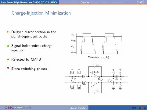
Charge-Injection Minimization
I Delayed disconnection in thesignal-dependent paths
I Signal-independent chargeinjection
I Rejected by CMFB
J Extra switching phases
Stepan Sutula
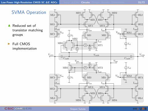
Low-Power High-Resolution CMOS SC ΔΣ ADCs Intro ΔΣMs Circuits Design Results Conclusions 33/72
SVMA OperationI Reduced set of
transistor matchinggroups
I Full CMOSimplementation
Stepan Sutula
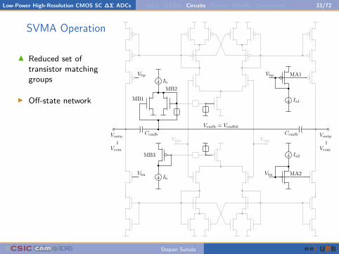
Low-Power High-Resolution CMOS SC ΔΣ ADCs Intro ΔΣMs Circuits Design Results Conclusions 33/72
SVMA OperationI Reduced set of
transistor matchinggroups
I Off-state network
Stepan Sutula
Low-Power High-Resolution CMOS SC ΔΣ ADCs Intro ΔΣMs Circuits Design Results Conclusions 33/72
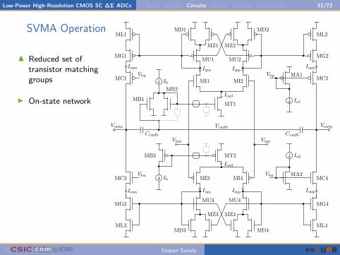
SVMA OperationI Reduced set of
transistor matchinggroups
I On-state network
Stepan Sutula
Low-Power High-Resolution CMOS SC ΔΣ ADCs Intro ΔΣMs Circuits Design Results Conclusions 33/72
1 Introduction
2 ΔΣ-Modulator Architectures
3 Low-Power CMOS Switched-Capacitor Circuits
4 Practical ΔΣM Design in a 0.18-µm CMOS Technology
5 Experimental Results
6 Conclusions
Stepan Sutula
Low-Power High-Resolution CMOS SC ΔΣ ADCs Intro ΔΣMs Circuits Design Results Conclusions 34/72
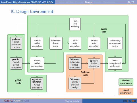
IC Design Environment
Stepan Sutula
Low-Power High-Resolution CMOS SC ΔΣ ADCs Intro ΔΣMs Circuits Design Results Conclusions 35/72
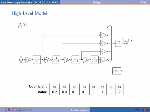
High-Level Model
Coefficient a1 a2 a3 a4 c1 c2 c3 c4Value 0.2 0.4 0.1 0.1 1 1 1 2
Stepan Sutula
Low-Power High-Resolution CMOS SC ΔΣ ADCs Intro ΔΣMs Circuits Design Results Conclusions 36/72
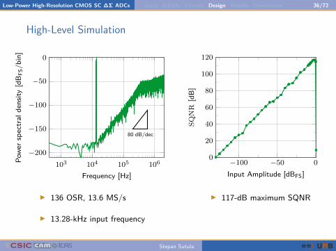
High-Level Simulation
103 104 105 106−200
−150
−100
−50
0
80 dB/dec
Frequency [Hz]
Powe
rspe
ctra
lden
sity
[dB F
S/bi
n]
−100 −50 00
20
40
60
80
100
120
Input Amplitude [dBFS]
SQN
R[d
B]I 136 OSR, 13.6 MS/s
I 13.28-kHz input frequency
I 117-dB maximum SQNR
Stepan Sutula
Low-Power High-Resolution CMOS SC ΔΣ ADCs Intro ΔΣMs Circuits Design Results Conclusions 37/72
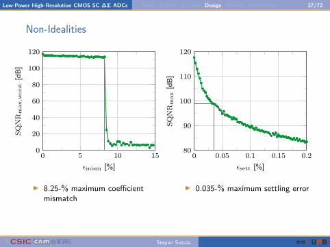
Non-Idealities
0 5 10 150
20
40
60
80
100
120
εmism [%]
SQN
Rm
ax,w
orst
[dB]
0 0.05 0.1 0.15 0.280
90
100
110
120
εsett [%]SQ
NR
max
[dB]
I 8.25-% maximum coefficientmismatch
I 0.035-% maximum settling error
Stepan Sutula
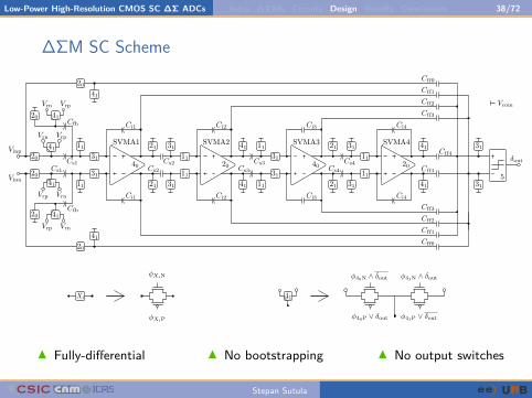
Low-Power High-Resolution CMOS SC ΔΣ ADCs Intro ΔΣMs Circuits Design Results Conclusions 38/72
ΔΣM SC SchemeI Fully-differential I No bootstrapping I No output switches
Stepan Sutula
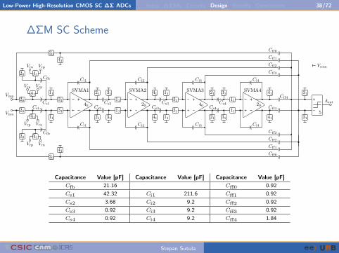
Low-Power High-Resolution CMOS SC ΔΣ ADCs Intro ΔΣMs Circuits Design Results Conclusions 38/72
ΔΣM SC Scheme
Capacitance Value [pF] Capacitance Value [pF] Capacitance Value [pF]Cfb 21.16 Cff0 0.92Cs1 42.32 Ci1 211.6 Cff1 0.92Cs2 3.68 Ci2 9.2 Cff2 0.92Cs3 0.92 Ci3 9.2 Cff3 0.92Cs4 0.92 Ci4 9.2 Cff4 1.84
Stepan Sutula
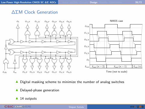
Low-Power High-Resolution CMOS SC ΔΣ ADCs Intro ΔΣMs Circuits Design Results Conclusions 39/72
ΔΣM Clock GenerationI Digital masking scheme to minimize the number of analog switches
I Delayed-phase generation
I 14 outputs
Stepan Sutula
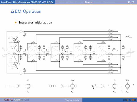
Low-Power High-Resolution CMOS SC ΔΣ ADCs Intro ΔΣMs Circuits Design Results Conclusions 40/72
ΔΣM Operation
I Integrator initialization
Stepan Sutula
Low-Power High-Resolution CMOS SC ΔΣ ADCs Intro ΔΣMs Circuits Design Results Conclusions 40/72
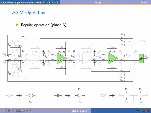
ΔΣM Operation
I Regular operation (phase A)
Stepan Sutula
Low-Power High-Resolution CMOS SC ΔΣ ADCs Intro ΔΣMs Circuits Design Results Conclusions 40/72
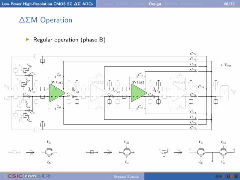
ΔΣM Operation
I Regular operation (phase B)
Stepan Sutula
Low-Power High-Resolution CMOS SC ΔΣ ADCs Intro ΔΣMs Circuits Design Results Conclusions 41/72
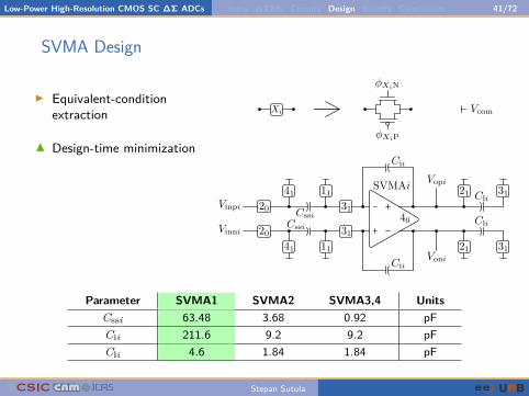
SVMA Design
I Equivalent-conditionextraction
I Design-time minimization
Parameter SVMA1 SVMA2 SVMA3,4 UnitsCssi 63.48 3.68 0.92 pFCii 211.6 9.2 9.2 pFCli 4.6 1.84 1.84 pF
Stepan Sutula
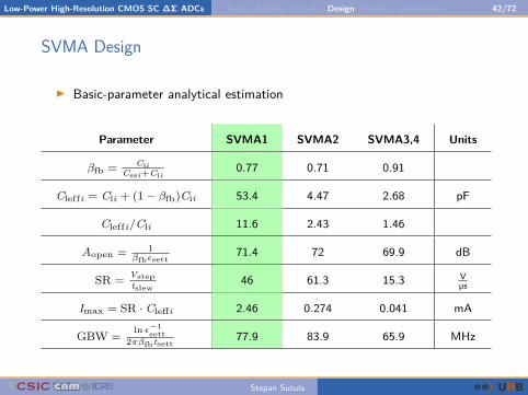
Low-Power High-Resolution CMOS SC ΔΣ ADCs Intro ΔΣMs Circuits Design Results Conclusions 42/72
SVMA Design
I Basic-parameter analytical estimation
Parameter SVMA1 SVMA2 SVMA3,4 Units
βfb = CiiCssi+Cii
0.77 0.71 0.91
Cleffi = Cli + (1 − βfb)Cii 53.4 4.47 2.68 pF
Cleffi/Cli 11.6 2.43 1.46
Aopen = 1βfbεsett
71.4 72 69.9 dB
SR = Vsteptslew
46 61.3 15.3 Vµs
Imax = SR · Cleffi 2.46 0.274 0.041 mA
GBW = ln ε−1sett
2πβfbtsett 77.9 83.9 65.9 MHz
Stepan Sutula
Low-Power High-Resolution CMOS SC ΔΣ ADCs Intro ΔΣMs Circuits Design Results Conclusions 43/72
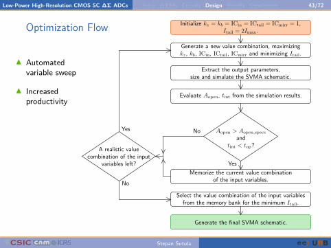
Optimization FlowI Automated
variable sweep
I Increasedproductivity
Stepan Sutula
Low-Power High-Resolution CMOS SC ΔΣ ADCs Intro ΔΣMs Circuits Design Results Conclusions 44/72
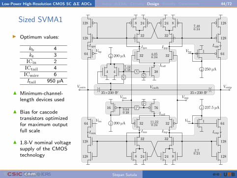
Sized SVMA1
I Optimum values:
kb 4kz 3
ICin 2ICtail 4ICmirr 6
Itail 950 µA
I Minimum-channel-length devices used
I Bias for cascodetransistors optimizedfor maximum outputfull scale
I 1.8-V nominal voltagesupply of the CMOStechnology
Stepan Sutula
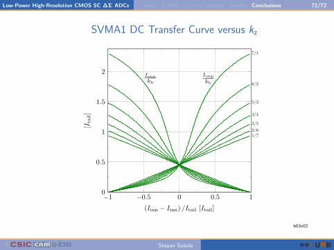
Low-Power High-Resolution CMOS SC ΔΣ ADCs Intro ΔΣMs Circuits Design Results Conclusions 45/72
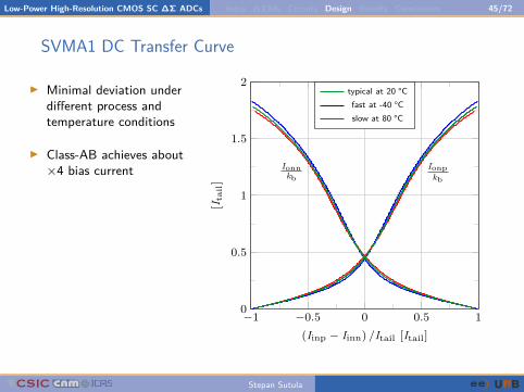
SVMA1 DC Transfer Curve
I Minimal deviation underdifferent process andtemperature conditions
I Class-AB achieves about×4 bias current
−1 −0.5 0 0.5 10
0.5
1
1.5
2
Ionnkb
Ionpkb
(Iinp − Iinn) /Itail [Itail]
[Ita
il]
typical at 20 °Cfast at -40 °Cslow at 80 °C
Stepan Sutula
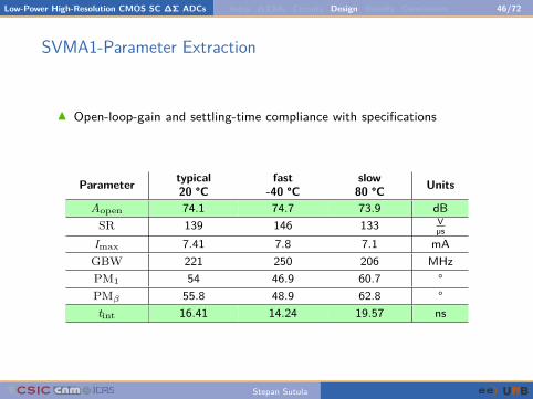
Low-Power High-Resolution CMOS SC ΔΣ ADCs Intro ΔΣMs Circuits Design Results Conclusions 46/72
SVMA1-Parameter ExtractionI Open-loop-gain and settling-time compliance with specifications
Parameter typical20 °C
fast-40 °C
slow80 °C Units
Aopen 74.1 74.7 73.9 dBSR 139 146 133 V
µsImax 7.41 7.8 7.1 mAGBW 221 250 206 MHzPM1 54 46.9 60.7 °PMβ 55.8 48.9 62.8 °tint 16.41 14.24 19.57 ns
Stepan Sutula
Low-Power High-Resolution CMOS SC ΔΣ ADCs Intro ΔΣMs Circuits Design Results Conclusions 47/72
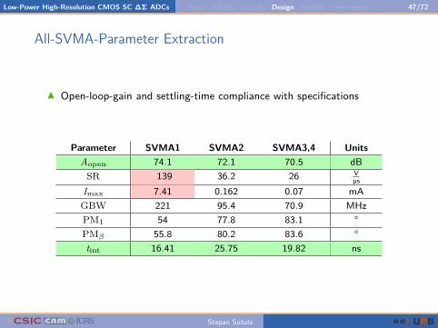
All-SVMA-Parameter ExtractionI Open-loop-gain and settling-time compliance with specifications
Parameter SVMA1 SVMA2 SVMA3,4 UnitsAopen 74.1 72.1 70.5 dB
SR 139 36.2 26 Vµs
Imax 7.41 0.162 0.07 mAGBW 221 95.4 70.9 MHzPM1 54 77.8 83.1 °PMβ 55.8 80.2 83.6 °tint 16.41 25.75 19.82 ns
Stepan Sutula
Low-Power High-Resolution CMOS SC ΔΣ ADCs Intro ΔΣMs Circuits Design Results Conclusions 48/72
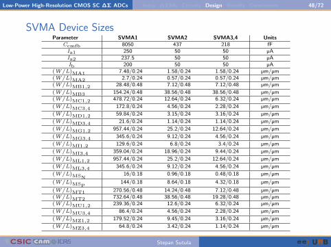
SVMA Device SizesParameter SVMA1 SVMA2 SVMA3,4 Units
Ccmfb 8050 437 218 fFIa1 250 50 50 µAIa2 237.5 50 50 µAIb 200 50 50 µA
(W/L)MA1 7.48/0.24 1.58/0.24 1.58/0.24 µm/µm(W/L)MA2 2.7/0.24 0.57/0.24 0.57/0.24 µm/µm(W/L)MB1,2 28.48/0.48 7.12/0.48 7.12/0.48 µm/µm(W/L)MB3 154.24/0.48 38.56/0.48 38.56/0.48 µm/µm(W/L)MC1,2 478.72/0.24 12.64/0.24 6.32/0.24 µm/µm(W/L)MC3,4 172.8/0.24 4.56/0.24 2.28/0.24 µm/µm(W/L)MD1,2 59.84/0.24 3.15/0.24 3.16/0.24 µm/µm(W/L)MD3,4 21.6/0.24 1.14/0.24 1.14/0.24 µm/µm(W/L)MG1,2 957.44/0.24 25.2/0.24 12.64/0.24 µm/µm(W/L)MG3,4 345.6/0.24 9.12/0.24 4.56/0.24 µm/µm(W/L)MI1,2 129.6/0.24 6.8/0.24 3.4/0.24 µm/µm(W/L)MI3,4 359.04/0.24 18.96/0.24 9.44/0.24 µm/µm(W/L)ML1,2 957.44/0.24 25.2/0.24 12.64/0.24 µm/µm(W/L)ML3,4 345.6/0.24 9.12/0.24 4.56/0.24 µm/µm(W/L)MSN
16/0.18 0.96/0.18 0.48/0.18 µm/µm(W/L)MSP
144/0.18 8.64/0.18 4.32/0.18 µm/µm(W/L)MT1 270.56/0.48 14.24/0.48 7.12/0.48 µm/µm(W/L)MT2 732.64/0.48 38.56/0.48 19.28/0.48 µm/µm(W/L)MU1,2 239.36/0.24 12.6/0.24 6.32/0.24 µm/µm(W/L)MU3,4 86.4/0.24 4.56/0.24 2.28/0.24 µm/µm(W/L)MZ1,2 179.52/0.24 9.45/0.24 3.16/0.24 µm/µm(W/L)MZ3,4 64.8/0.24 3.42/0.24 1.14/0.24 µm/µm
Stepan Sutula
Low-Power High-Resolution CMOS SC ΔΣ ADCs Intro ΔΣMs Circuits Design Results Conclusions 49/72
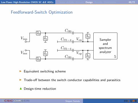
Feedforward-Switch Optimization
I Equivalent switching scheme
I Trade-off between the switch conductor capabilities and parasitics
I Design-time reduction
Stepan Sutula
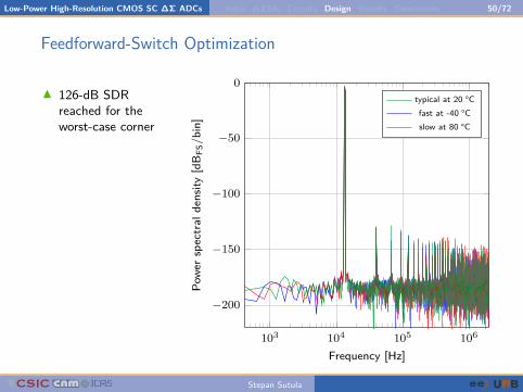
Low-Power High-Resolution CMOS SC ΔΣ ADCs Intro ΔΣMs Circuits Design Results Conclusions 50/72
Feedforward-Switch OptimizationI 126-dB SDR
reached for theworst-case corner
103 104 105 106
0
−50
−100
−150
−200
Frequency [Hz]
Powe
rspe
ctra
lden
sity
[dB F
S/bi
n]
typical at 20 °Cfast at -40 °Cslow at 80 °C
Stepan Sutula
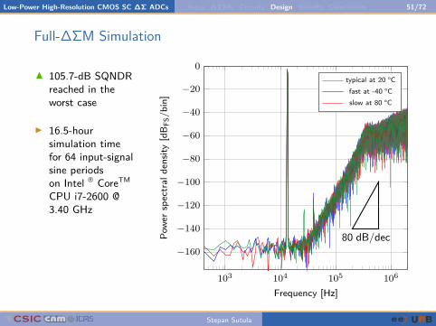
Low-Power High-Resolution CMOS SC ΔΣ ADCs Intro ΔΣMs Circuits Design Results Conclusions 51/72
Full-ΔΣM SimulationI 105.7-dB SQNDR
reached in theworst case
I 16.5-hoursimulation timefor 64 input-signalsine periodson Intel ® CoreTMCPU i7-2600 @3.40 GHz
103 104 105 106
0
−20
−40
−60
−80
−100
−120
−140
−16080 dB/dec
Frequency [Hz]
Powe
rspe
ctra
lden
sity
[dB F
S/bi
n]
typical at 20 °Cfast at -40 °Cslow at 80 °C
Stepan Sutula
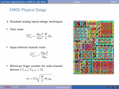
Low-Power High-Resolution CMOS SC ΔΣ ADCs Intro ΔΣMs Circuits Design Results Conclusions 52/72
CMOS Physical DesignI Standard analog layout-design techniques
I Gate noise:
V 2n,g = 4kBT3m2
WL R�
I Input-referred channel noise:
V 2n,ch = 8kBT
3gm
I Minimum finger number for wide-channeldevices (Vn,ch/Vg,ch = 5):
m = 3.5√
WL R�gm
Stepan Sutula
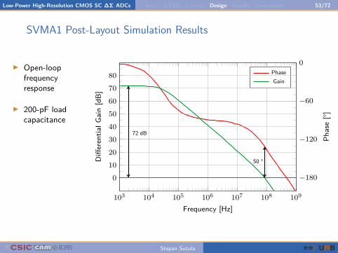
Low-Power High-Resolution CMOS SC ΔΣ ADCs Intro ΔΣMs Circuits Design Results Conclusions 53/72
SVMA1 Post-Layout Simulation Results
I Open-loopfrequencyresponse
I 200-pF loadcapacitance
103 104 105 106 107 108 109
0
−60
−120
−180
Frequency [Hz]
Phase[°]
PhaseGain
01020304050607080
72 dB
50 °Differentia
lGain[dB]
Stepan Sutula
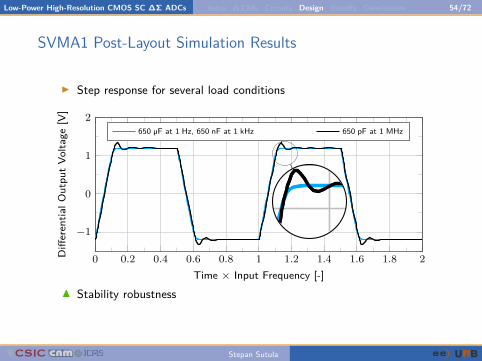
Low-Power High-Resolution CMOS SC ΔΣ ADCs Intro ΔΣMs Circuits Design Results Conclusions 54/72
SVMA1 Post-Layout Simulation Results
I Step response for several load conditions
0 0.2 0.4 0.6 0.8 1 1.2 1.4 1.6 1.8 2
−1
0
1
2
Time × Input Frequency [-]
Differentia
lOutpu
tVo
ltage
[V]
650 µF at 1 Hz, 650 nF at 1 kHz 650 pF at 1 MHz
0 0.2 0.4 0.6 0.8 1 1.2 1.4 1.6 1.8 2
−1
0
1
2
Time × Input Frequency [-]
Differentia
lOutpu
tVo
ltage
[V]
650 µF at 1 Hz, 650 nF at 1 kHz 650 pF at 1 MHz
I Stability robustness
Stepan Sutula
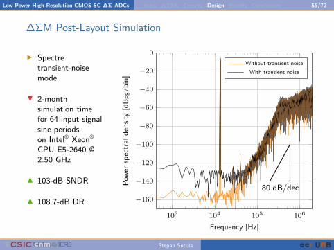
Low-Power High-Resolution CMOS SC ΔΣ ADCs Intro ΔΣMs Circuits Design Results Conclusions 55/72
ΔΣM Post-Layout Simulation
I Spectretransient-noisemode
J 2-monthsimulation timefor 64 input-signalsine periodson Intel® Xeon®
CPU E5-2640 @2.50 GHz
I 103-dB SNDR
I 108.7-dB DR103 104 105 106
0
−20
−40
−60
−80
−100
−120
−140
−16080 dB/dec
Frequency [Hz]
Powe
rspe
ctra
lden
sity
[dB F
S/bi
n]
Without transient noiseWith transient noise
Stepan Sutula
Low-Power High-Resolution CMOS SC ΔΣ ADCs Intro ΔΣMs Circuits Design Results Conclusions 56/72
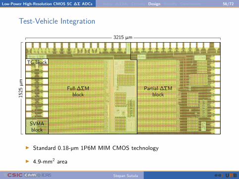
Test-Vehicle Integration
I Standard 0.18-µm 1P6M MIM CMOS technology
I 4.9-mm2 area
Stepan Sutula
Low-Power High-Resolution CMOS SC ΔΣ ADCs Intro ΔΣMs Circuits Design Results Conclusions 57/72
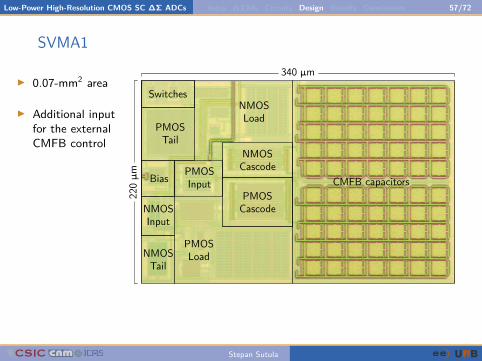
SVMA1
I 0.07-mm2 area
I Additional inputfor the externalCMFB control
Stepan Sutula
Low-Power High-Resolution CMOS SC ΔΣ ADCs Intro ΔΣMs Circuits Design Results Conclusions 58/72
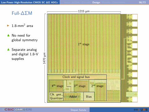
Full-ΔΣM
I 1.8-mm2 area
I No need forglobal symmetry
I Separate analogand digital 1.8-Vsupplies
Stepan Sutula
Low-Power High-Resolution CMOS SC ΔΣ ADCs Intro ΔΣMs Circuits Design Results Conclusions 58/72
1 Introduction
2 ΔΣ-Modulator Architectures
3 Low-Power CMOS Switched-Capacitor Circuits
4 Practical ΔΣM Design in a 0.18-µm CMOS Technology
5 Experimental Results
6 Conclusions
Stepan Sutula
Low-Power High-Resolution CMOS SC ΔΣ ADCs Intro ΔΣMs Circuits Design Results Conclusions 59/72
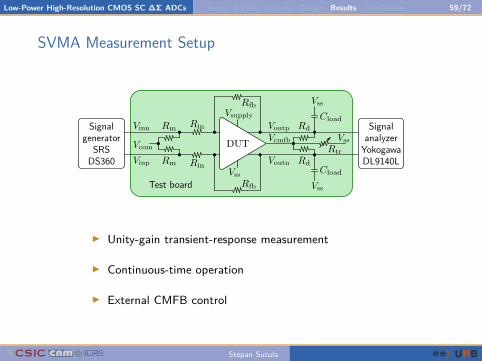
SVMA Measurement Setup
I Unity-gain transient-response measurement
I Continuous-time operation
I External CMFB control
Stepan Sutula
Low-Power High-Resolution CMOS SC ΔΣ ADCs Intro ΔΣMs Circuits Design Results Conclusions 60/72
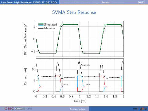
SVMA Step Response
Stepan Sutula
Low-Power High-Resolution CMOS SC ΔΣ ADCs Intro ΔΣMs Circuits Design Results Conclusions 61/72
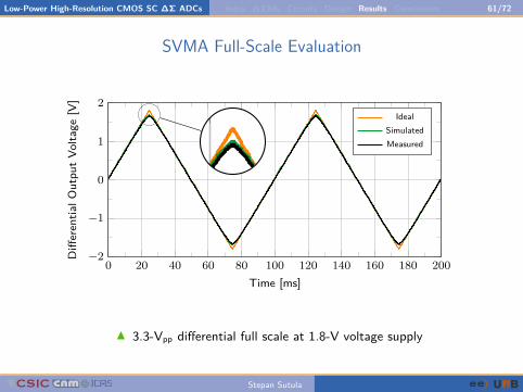
SVMA Full-Scale Evaluation
0 20 40 60 80 100 120 140 160 180 200−2
−1
0
1
2
Time [ms]
Differentia
lOutpu
tVo
ltage
[V]
IdealSimulatedMeasured
0 20 40 60 80 100 120 140 160 180 200−2
−1
0
1
2
Time [ms]
Differentia
lOutpu
tVo
ltage
[V]
IdealSimulatedMeasured
I 3.3-Vpp differential full scale at 1.8-V voltage supply
Stepan Sutula
Low-Power High-Resolution CMOS SC ΔΣ ADCs Intro ΔΣMs Circuits Design Results Conclusions 62/72
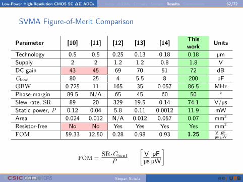
SVMA Figure-of-Merit Comparison
Parameter [10] [11] [12] [13] [14] Thiswork Units
Technology 0.5 0.5 0.25 0.13 0.18 0.18 µmSupply 2 2 1.2 1.2 0.8 1.8 VDC gain 43 45 69 70 51 72 dBCload 80 25 4 5.5 8 200 pFGBW 0.725 11 165 35 0.057 86.5 MHzPhase margin 89.5 N/A 65 45 60 50 °Slew rate, SR 89 20 329 19.5 0.14 74.1 V/µsStatic power, P 0.12 0.04 5.8 0.11 0.0012 11.9 mWArea 0.024 0.012 N/A 0.012 0.057 0.07 mm2
Resistor-free No No Yes Yes Yes Yes mm2
FOM 59.33 12.50 0.28 0.98 0.93 1.25 Vµs
pFµW
FOM = SR·CloadP
[Vµs
pFµW
]
Stepan Sutula
Low-Power High-Resolution CMOS SC ΔΣ ADCs Intro ΔΣMs Circuits Design Results Conclusions 63/72
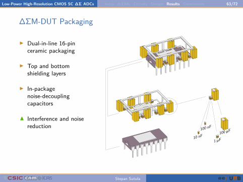
ΔΣM-DUT Packaging
I Dual-in-line 16-pinceramic packaging
I Top and bottomshielding layers
I In-packagenoise-decouplingcapacitors
I Interference and noisereduction
Stepan Sutula
Low-Power High-Resolution CMOS SC ΔΣ ADCs Intro ΔΣMs Circuits Design Results Conclusions 64/72
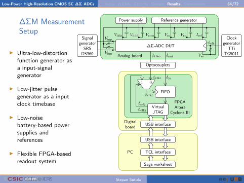
ΔΣM MeasurementSetup
I Ultra-low-distortionfunction generator asa input-signalgenerator
I Low-jitter pulsegenerator as a inputclock timebase
I Low-noisebattery-based powersupplies andreferences
I Flexible FPGA-basedreadout system
Stepan Sutula
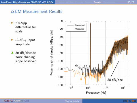
Low-Power High-Resolution CMOS SC ΔΣ ADCs Intro ΔΣMs Circuits Design Results Conclusions 65/72
ΔΣM Measurement Results
I 2.4-Vppdifferential fullscale
I -2-dBFS inputamplitude
I 80-dB/decadenoise-shapingslope observed
103 104 105 106
0
−20
−40
−60
−80
−100
−120
−140
−16080 dB/dec
Frequency [Hz]
Powe
rspe
ctra
lden
sity
[dB F
S/bi
n]
SimulatedMeasured
Stepan Sutula
Low-Power High-Resolution CMOS SC ΔΣ ADCs Intro ΔΣMs Circuits Design Results Conclusions 66/72
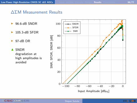
ΔΣM Measurement Results
I 96.6-dB SNDR
I 105.3-dB SFDR
I 97-dB DR
I SNDRdegradation athigh amplitudes isavoided
−100 −80 −60 −40 −20 00
20
40
60
80
100
Input Amplitude [dBFS]
SNR,
SFD
R,SN
DR
[dB]
SNDRSFDRSNR
Stepan Sutula
Low-Power High-Resolution CMOS SC ΔΣ ADCs Intro ΔΣMs Circuits Design Results Conclusions 67/72
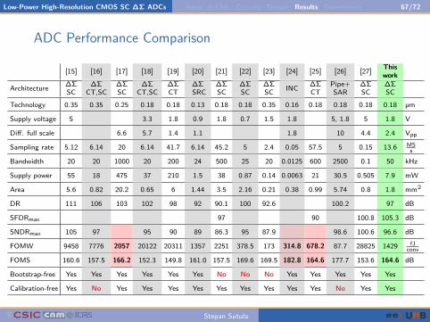
ADC Performance Comparison
[15] [16] [17] [18] [19] [20] [21] [22] [23] [24] [25] [26] [27] Thiswork
Architecture ΔΣSC
ΔΣCT,SC
ΔΣSC
ΔΣCT,SC
ΔΣCT
ΔΣSRC
ΔΣSC
ΔΣSC
ΔΣSC INC ΔΣ
CTPipe+SAR
ΔΣSC
ΔΣSC
Technology 0.35 0.35 0.25 0.18 0.18 0.13 0.18 0.18 0.35 0.16 0.18 0.18 0.18 0.18 µm
Supply voltage 5 3.3 1.8 0.9 1.8 0.7 1.5 1.8 5, 1.8 5 1.8 V
Diff. full scale 6.6 5.7 1.4 1.1 1.8 10 4.4 2.4 Vpp
Sampling rate 5.12 6.14 20 6.14 41.7 6.14 45.2 5 2.4 0.05 57.5 5 0.15 13.6 MSs
Bandwidth 20 20 1000 20 200 24 500 25 20 0.0125 600 2500 0.1 50 kHz
Supply power 55 18 475 37 210 1.5 38 0.87 0.14 0.0063 21 30.5 0.505 7.9 mW
Area 5.6 0.82 20.2 0.65 6 1.44 3.5 2.16 0.21 0.38 0.99 5.74 0.8 1.8 mm2
DR 111 106 103 102 98 92 90.1 100 92.6 100.2 97 dB
SFDRmax 97 90 100.8 105.3 dB
SNDRmax 105 97 95 90 89 86.3 95 87.9 98.6 100.6 96.6 dB
FOMW 9458 7776 2057 20122 20311 1357 2251 378.5 173 314.8 678.2 87.7 28825 1429 fJconv
FOMS 160.6 157.5 166.2 152.3 149.8 161.0 157.5 169.6 169.5 182.8 164.6 177.7 153.6 164.6 dB
Bootstrap-free Yes Yes Yes Yes Yes Yes No No No Yes Yes Yes Yes Yes
Calibration-free Yes No Yes Yes Yes Yes Yes Yes Yes Yes Yes No Yes Yes
Stepan Sutula
Low-Power High-Resolution CMOS SC ΔΣ ADCs Intro ΔΣMs Circuits Design Results Conclusions 68/72
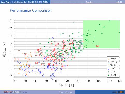
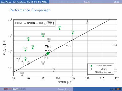
Performance Comparison
20 30 40 50 60 70 80 90 100 110 120100
101
102
103
104
105
106
107
SNDR [dB]
P/f sn
yq[p
J]
FlashFoldingPipeline
SARCT ΔΣSC ΔΣ
Stepan Sutula
Low-Power High-Resolution CMOS SC ΔΣ ADCs Intro ΔΣMs Circuits Design Results Conclusions 68/72
Performance Comparison
85 90 95 100 105 110 115 120
104
105
106
107FOMS = SNDR + 10 log
(BW
P
)
[28][29]
[15][18]
[19]
[20]
[27]
[30]
[17] [24]
[25]
[31]
[32]
[33]
[16]
[21] [22]
[23]
[26]
Thiswork
SNDR [dB]
P/f sn
yq[pJ]
Feature-compliantOthers
FOMS of this work
Stepan Sutula
Low-Power High-Resolution CMOS SC ΔΣ ADCs Intro ΔΣMs Circuits Design Results Conclusions 68/72
1 Introduction
2 ΔΣ-Modulator Architectures
3 Low-Power CMOS Switched-Capacitor Circuits
4 Practical ΔΣM Design in a 0.18-µm CMOS Technology
5 Experimental Results
6 Conclusions
Stepan Sutula
Low-Power High-Resolution CMOS SC ΔΣ ADCs Intro ΔΣMs Circuits Design Results Conclusions 69/72
Contributions
I Initial working hypotheses successively tested and confirmed:• High-resolution and low-power state-of-the-art ADC• Integrated in a low-cost standard CMOS technology• Using novel analog design techniques at the system and circuit
levels• No bootstrapping, analog calibration or digital
post-compensationI Selection guide of SC ΔΣM ADCsI Efficient framework based on open-source EDA toolsI New family of single-stage Class-AB OpAmps: VMAsI SVMA- and ΔΣM-demonstrator implementation and measurements
Stepan Sutula
Low-Power High-Resolution CMOS SC ΔΣ ADCs Intro ΔΣMs Circuits Design Results Conclusions 70/72
Research Funding
2007-2011: Chemical Warfare Agents Analyzer Based onLow Cost Dual Band IR Microsystem (CANARIO)EDA-B-DO61-IAP2-ERG:32-channel read-out low-power IC
2009-2012: Perishable Monitoring through Short Tracking ofLifetime and Quality by RFID (PASTEUR)CATRENE CT204:Low-power smart sensor with integratedpotentiostatic ΔΣ ADC
2011-2015: ESA Cosmic Vision MF ASICESTEC 40000101556/10/NL/AF:4 low-power ΔΣ ADCs with multiple BWs and SNDRs
Stepan Sutula
Low-Power High-Resolution CMOS SC ΔΣ ADCs Intro ΔΣMs Circuits Design Results Conclusions 71/72
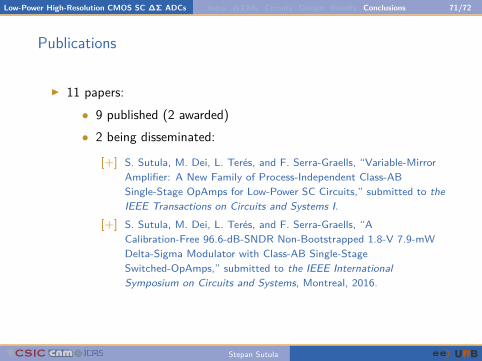
Publications
I 11 papers:• 9 published (2 awarded)• 2 being disseminated:
[+] S. Sutula, M. Dei, L. Terés, and F. Serra-Graells, “Variable-MirrorAmplifier: A New Family of Process-Independent Class-ABSingle-Stage OpAmps for Low-Power SC Circuits,” submitted to theIEEE Transactions on Circuits and Systems I.
[+] S. Sutula, M. Dei, L. Terés, and F. Serra-Graells, “ACalibration-Free 96.6-dB-SNDR Non-Bootstrapped 1.8-V 7.9-mWDelta-Sigma Modulator with Class-AB Single-StageSwitched-OpAmps,” submitted to the IEEE InternationalSymposium on Circuits and Systems, Montreal, 2016.
Stepan Sutula
Low-Power High-Resolution CMOS SC ΔΣ ADCs Intro ΔΣMs Circuits Design Results Conclusions 72/72
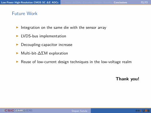
Future Work
I Integration on the same die with the sensor array
I LVDS-bus implementation
I Decoupling-capacitor increase
I Multi-bit-ΔΣM exploration
I Reuse of low-current design techniques in the low-voltage realm
Thank you!
Stepan Sutula
Low-Power High-Resolution CMOS SC ΔΣ ADCs Intro ΔΣMs Circuits Design Results Conclusions 72/72
References[1] S. Sutula, M. Dei, L. Terés, and F. Serra-Graells, “Class-AB Single-Stage
OpAmp for Low-Power Switched-Capacitor Circuits,” in Proceedings of the IEEEInternational Symposium on Circuits and Systems, pp. 2081–2084, 2015,Student Best Paper Award Honorable Mention.
[2] S. Sutula, F. Vila, J. Pallarès, K. Sabine, L. Terés, and F. Serra-Graells,“Teaching Mixed-Mode Full-Custom VLSI Design with gaf, SpiceOpus andGlade,” in Proceedings of the 10th European Workshop on MicroelectronicsEducation, pp. 43–48, 2014.
[3] J. Pallarès, F. Vila, S. Sutula, K. Sabine, L. Terés, and F. Serra-Graells, “AFreeware EDA Framework for Teaching Mixed-Mode Full-Custom VLSI Design,”in Proceedings of the XIX Conference on Design of Circuits and IntegratedSystems, 2014.
[4] S. Sutula, J. Pallarès Cuxart, J. Gonzalo-Ruiz, F. Xavier Munoz-Pascual,L. Terés, and F. Serra-Graells, “A 25-uW All-MOS Potentiostatic Delta-SigmaADC for Smart Electrochemical Sensors,” IEEE Transactions on Circuits andSystems I: Regular Papers, vol. 61, pp. 671–679, 2014.
[5] J. Pallarès, S. Sutula, J. Gonzalo-Ruiz, F. X. Muñoz-Pascual, L. Terés, andF. Serra-Graells, “A Low-Power MOS-Only Potentiostatic Delta-Sigma ADCArchitecture for Electrochemical Sensors,” in Proceedings of the XIX Conferenceon Design of Circuits and Integrated Systems, 2014, Best Paper Award.
Stepan Sutula
Low-Power High-Resolution CMOS SC ΔΣ ADCs Intro ΔΣMs Circuits Design Results Conclusions 72/72
[6] S. Sutula, C. Ferrer, and F. Serra-Graells, “Design and Modeling of a Low-PowerMulti-Channel Integrated Circuit for Infrared Gas Recognition,” ElsevierMicroprocessors and Microsystems, vol. 36, pp. 355–364, 2012.
[7] S. Sutula, C. Ferrer, and F. Serra-Graells, “A 400 µW Hz-Range Lock-In A/DFrontend Channel for Infrared Spectroscopic Gas Recognition,” IEEETransactions on Circuits and Systems I: Regular Papers, vol. 58, pp. 1561–1568,2011.
[8] S. Sutula, C. Ferrer, and F. Serra-Graells, “A 100µA/Ch Fully-Integrable Lock-inMulti-Channel Frontend for Infrared Spectroscopic Gas Recognition,” inProceedings of the IEEE International Symposium on Circuits and Systems,pp. 2267–2270, 2010.
[9] S. Sutula, C. Ferrer, and F. Serra-Graells, “Design and Modeling of a 0.4mW/ChMulti-Channel Integrated Circuit for Infrared Gas Recognition,” in Proceedings ofthe XXV Conference on Design of Circuits and Integrated Systems, pp. 226–271,2010.
[10] A. J. López-Martín, S. Baswa, J. Ramirez-Angulo, and R. G. Carvajal,“Low-Voltage Super Class AB CMOS OTA Cells With Very High Slew Rate andPower Efficiency,” IEEE Journal of Solid-State Circuits, vol. 40, pp. 1068–1077,2005.
[11] J. Ramirez-Angulo, R. G. Carvajal, J. A. Galan, and A. Lopez-Martin, “A FreeBut Efficient Low-Voltage Class-AB Two-Stage Operational Amplifier,” IEEE
Stepan Sutula
Low-Power High-Resolution CMOS SC ΔΣ ADCs Intro ΔΣMs Circuits Design Results Conclusions 72/72
Transactions on Circuits and Systems II: Expressed Briefs, vol. 53, pp. 568–571,2006.
[12] M. Yavary and O. Shoaei, “Very Low-Voltage, Low-Power and Fast-Settling OTAfor Switched-Capacitor Applications,” in Proceedings of the InternationalConference on Microelectronics, pp. 10–13, 2002.
[13] M. Figueiredo, R. Santos-Tavares, E. Santin, J. Ferreira, G. Evans, and J. Goes,“A Two-Stage Fully Differential Inverter-Based Self-Biased CMOS AmplifierWith High Efficiency,” IEEE Transactions on Circuits and Systems I: RegularPapers, vol. 58, pp. 1591–1603, 2011.
[14] M. R. Valero, S. Celma, N. Medrano, B. Calvo, and C. Azcona, “An UltraLow-Power Low-Voltage Class AB CMOS Fully Differential OpAmp,” inProceedings of the IEEE International Symposium on Circuits and Systems,pp. 1967–1970, 2012.
[15] Y. Yang, A. Chokhawala, M. Alexander, J. Melanson, and D. Hester, “A 114-dB68-mW Chopper-Stabilized Stereo Multi-bit Audio A/D Converter,” inProceedings of the IEEE International Solid-State Circuits Conference,pp. 56–477, 2003.
[16] K. Nguyen, B. Adams, K. Sweetland, H. Chen, and K. McLaughlin, “A 106dBSNR Hybrid Oversampling ADC for Digital Audio,” in Proceedings of the IEEEInternational Solid-State Circuits Conference, pp. 176–591, 2005.
Stepan Sutula
Low-Power High-Resolution CMOS SC ΔΣ ADCs Intro ΔΣMs Circuits Design Results Conclusions 72/72
[17] R. Brewer, J. Gorbold, P. Hurrell, C. Lyden, R. Maurino, and M. Vickery, “A100dB SNR 2.5MS/s Output Data Rate ΔΣ ADC,” in Proceedings of the IEEEInternational Solid-State Circuits Conference, pp. 172–173, 2005.
[18] P. Morrow, M. Chamarro, C. Lyden, P. Ventura, A. Abo, A. Matamura,M. Keane, R. O’Brien, P. Minogue, J. Mansson, N. McGuinness,M. McGranaghan, and I. Ryan, “A 0.18µm 102dB-SNR Mixed CT SCAudio-Band ΔΣ ADC,” in Proceedings of the IEEE International Solid-StateCircuits Conference, pp. 178–592, 2005.
[19] P. Silva, L. Breems, K. Makinwa, R. Roovers, and J. Huijsing, “An 118dB DRCT IF-to-Baseband ΣΔ Modulator for AM/FM/IBOC Radio Receivers,” inProceedings of the IEEE International Solid-State Circuits Conference,pp. 151–160, 2006.
[20] M. Kim, G. Ahn, P. Hanumolu, S. Lee, S. Kim, S. You, J. Kim, G. Temes, andU. Moon, “A 0.9V 92dB Double-Sampled Switched-RC ΔΣ Audio ADC,” inSymposium on VLSI Circuits Digest of Technical Papers, pp. 160–161, 2006.
[21] A. Agah, K. Vleugels, P. Griffin, M. Ronaghi, J. Plummer, and B. Wooley, “AHigh-Resolution Low-Power Oversampling ADC with Extended-Range forBio-Sensor Arrays,” in Symposium on VLSI Circuits Digest of Technical Papers,pp. 244–245, 2007.
[22] H. Park, K. Nam, D. K. Su, K. Vleugels, and B. A. Wooley, “A 0.7-V 100-dB870-µW Digital Audio ΔΣ Modulator,” in Symposium on VLSI Circuits Digest ofTechnical Papers, pp. 178–179, 2008.
Stepan Sutula
Low-Power High-Resolution CMOS SC ΔΣ ADCs Intro ΔΣMs Circuits Design Results Conclusions 72/72
[23] T. Christen, “A 15bit 140µW Scalable-Bandwidth Inverter-Based Audio ΔΣModulator with >78dB PSRR,” in Proceedings of the European Solid-StateCircuits Conference, pp. 209–212, 2012.
[24] Y. Chae, K. Souri, and K. Makinwa, “A 6.3µW 20b Incremental Zoom-ADC with6ppm INL and 1µV Offset,” in Proceedings of the IEEE International Solid-StateCircuits Conference, pp. 276–277, 2013.
[25] A. Bandyopadhyay, R. Adams, N. Khiem, P. Baginski, D. Lamb, and T. Tansley,“A 97.3 dB SNR, 600 kHz BW, 31mW Multibit Continuous Time ΔΣ ADC,” inSymposium on VLSI Circuits Digest of Technical Papers, pp. 1–2, 2014.
[26] A. Bannon, C. Hurrell, D. Hummerston, and C. Lyden, “An 18 b 5 MS/s SARADC with 100.2 dB Dynamic Range,” in Symposium on VLSI Circuits Digest ofTechnical Papers, pp. 1–2, 2014.
[27] L. Xu, B. Gönen, Q. Fan, J. Huijsing, and K. A. A. Makinwa, “A 110dB SNRADC with ±30V Input Common-Mode Range and 8µV Offset for CurrentSensing Applications,” in Proceedings of the IEEE International Solid-StateCircuits Conference, pp. 90–91, 2015.
[28] Y. Matsuya and J. Terada, “1.2-V, 16-bit Audio A/D Converter With SuppressedLatch Error Noise,” in Symposium on VLSI Circuits Digest of Technical Papers,pp. 19–20, 1997.
Stepan Sutula
Low-Power High-Resolution CMOS SC ΔΣ ADCs Intro ΔΣMs Circuits Design Results Conclusions 72/72
[29] Y. Geerts, M. Steyaert, and W. Sansen, “A 2.5MSample/s Multi-Bit ΔΣ CMOSADC with 95dB SNR,” in Proceedings of the IEEE International Solid-StateCircuits Conference, pp. 336–337, 2000.
[30] E. Zwan, “A 2.3 mW CMOS ΣΔ Modulator for Audio Applications,” inProceedings of the IEEE International Solid-State Circuits Conference,pp. 220–221, 1997.
[31] K. Y. Leung, E. J. Swanson, K. Leung, and S. S. Zhu, “A 5V, 118dB ΔΣAnalog-to-Digital Converter for Wideband Digital Audio,” in Proceedings of theIEEE International Solid-State Circuits Conference, pp. 218–219, 1997.
[32] A. L. Coban and P. E. Allen, “A 1.5V 1.0mW Audio Σ∆ Modulator with 98dBDynamic Range,” in Proceedings of the International Solid-State CircuitsConference, pp. 50–51, IEEE, 1999.
[33] K. Vleugels, S. Rabii, and B. A. Wooley, “A 2.5V Broadband Multi-Bit ΔΣModulator with 95dB Dynamic Range,” in Proceedings of the IEEE InternationalSolid-State Circuits Conference, pp. 50–51, 2001.
Stepan Sutula
Low-Power High-Resolution CMOS SC ΔΣ ADCs Intro ΔΣMs Circuits Design Results Conclusions 72/72
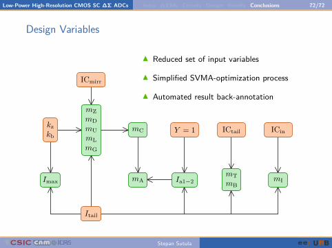
Design Variables
I Reduced set of input variables
I Simplified SVMA-optimization process
I Automated result back-annotation
Stepan Sutula
Low-Power High-Resolution CMOS SC ΔΣ ADCs Intro ΔΣMs Circuits Design Results Conclusions 72/72
SVMA1 DC Transfer Curve versus kz
b03v02
Stepan Sutula