Embed Size (px)
Citation preview
ASCTB387E 201912Panasonic Corporation 2019
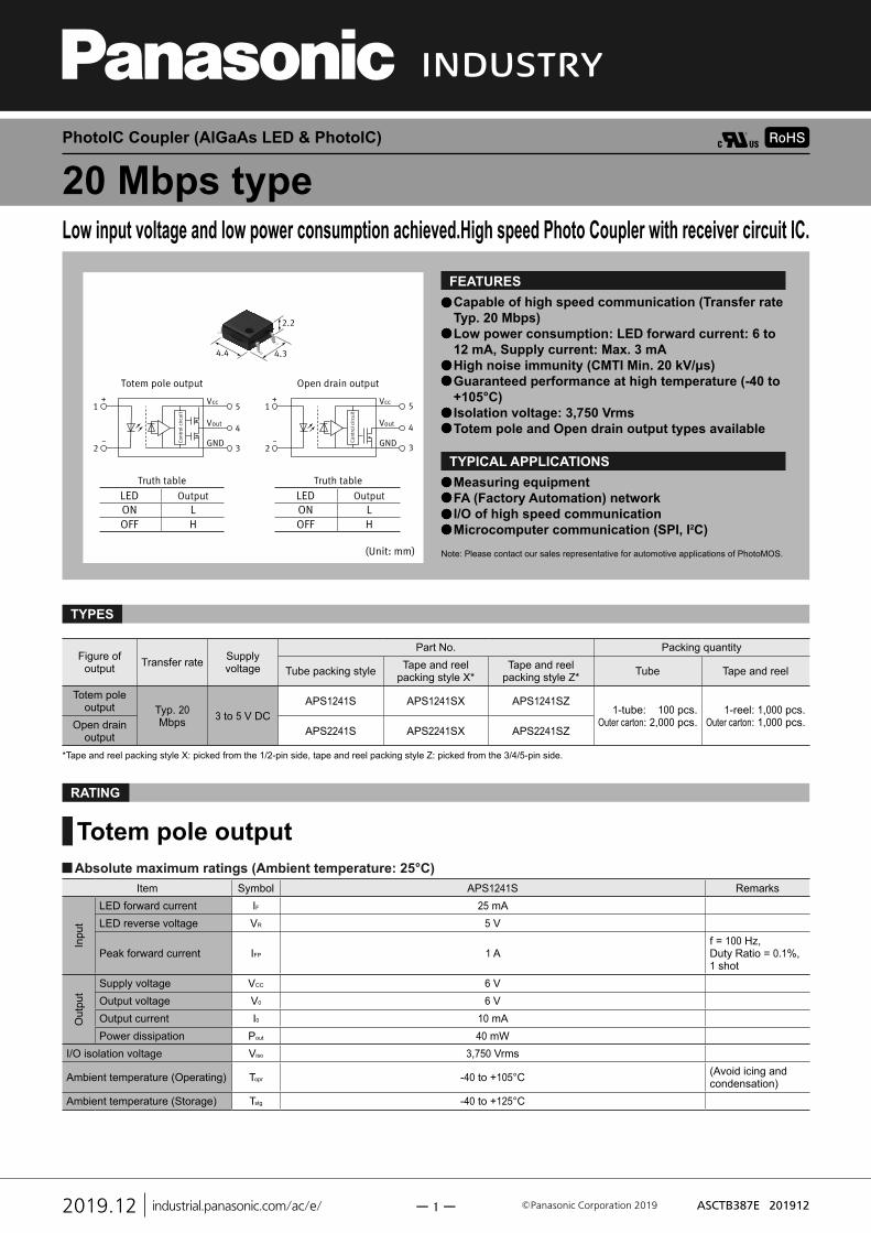
FEATURESCapable of high speed communication (Transfer rate Typ. 20 Mbps)Low power consumption: LED forward current: 6 to 12 mA, Supply current: Max. 3 mAHigh noise immunity (CMTI Min. 20 kV/μs)Guaranteed performance at high temperature (-40 to +105°C)Isolation voltage: 3,750 VrmsTotem pole and Open drain output types available
Low input voltage and low power consumption achieved.High speed Photo Coupler with receiver circuit IC.20 Mbps typePhotoIC Coupler (AlGaAs LED & PhotoIC)
TYPICAL APPLICATIONSMeasuring equipmentFA (Factory Automation) networkI/O of high speed communicationMicrocomputer communication (SPI, I2C)
Note: Please contact our sales representative for automotive applications of PhotoMOS.
LEDON LOFF H
LEDON LOFF H
2.2
4.34.4
2
1
3
5
4
GND
Vcc
Vout
+
ー2
1
3
5
4
GND
Vcc
Vout
+
ー
Totem pole output Open drain output
Truth tableOutput
Truth tableOutput
(Unit: mm)
Cont
rol c
ircui
t
Cont
rol c
ircui
t
TYPES
Figure of output Transfer rate Supply
voltage
Part No. Packing quantity
Tube packing style Tape and reelpacking style X*
Tape and reelpacking style Z* Tube Tape and reel
Totem pole output Typ. 20
Mbps 3 to 5 V DCAPS1241S APS1241SX APS1241SZ
1-tube: 100 pcs.Outer carton: 2,000 pcs.
1-reel: 1,000 pcs.Outer carton: 1,000 pcs.Open drain
output APS2241S APS2241SX APS2241SZ
*Tape and reel packing style X: picked from the 1/2-pin side, tape and reel packing style Z: picked from the 3/4/5-pin side.
Totem pole outputAbsolute maximum ratings (Ambient temperature: 25°C)
Item Symbol APS1241S Remarks
Inpu
t
LED forward current IF 25 mALED reverse voltage VR 5 V
Peak forward current IFP 1 Af = 100 Hz,Duty Ratio = 0.1%,1 shot
Out
put
Supply voltage VCC 6 VOutput voltage V0 6 VOutput current I0 10 mAPower dissipation Pout 40 mW
I/O isolation voltage Viso 3,750 Vrms
Ambient temperature (Operating) Topr -40 to +105°C (Avoid icing and condensation)
Ambient temperature (Storage) Tstg -40 to +125°C
RATING
industrial.panasonic.com/ac/e/2019.12 ー 1 ー
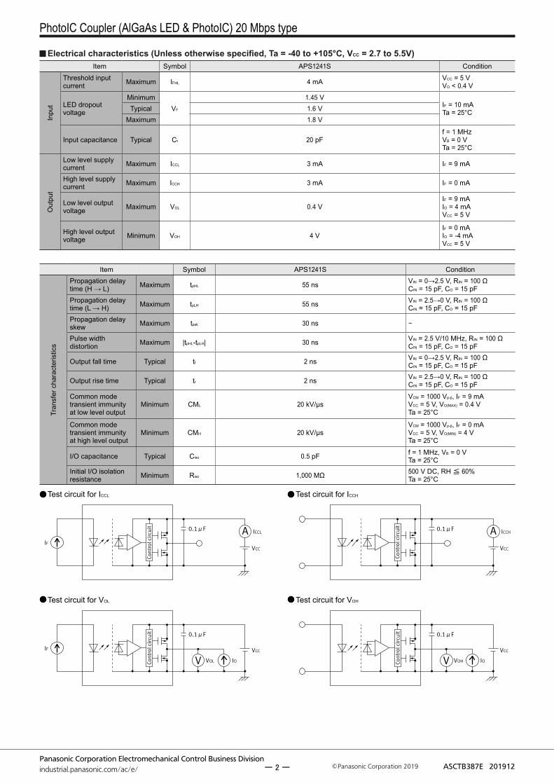
PhotoIC Coupler (AlGaAs LED & PhotoIC) 20 Mbps type
Panasonic Corporation Electromechanical Control Business Divisionindustrial.panasonic.com/ac/e/ ASCTB387E 201912Panasonic Corporation 2019
A ICCL
VCC
0.1μF
IF
Cont
rol c
ircui
t
Test circuit for ICCL
Electrical characteristics (Unless otherwise specified, Ta = -40 to +105°C, VCC = 2.7 to 5.5V)Item Symbol APS1241S Condition
Inpu
t
Threshold input current Maximum IFHL 4 mA VCC = 5 V
VO < 0.4 V
LED dropout voltage
MinimumVF
1.45 VIF = 10 mA Ta = 25°CTypical 1.6 V
Maximum 1.8 V
Input capacitance Typical Ct 20 pFf = 1 MHz VB = 0 VTa = 25°C
Out
put
Low level supplycurrent Maximum ICCL 3 mA IF = 9 mA
High level supplycurrent Maximum ICCH 3 mA IF = 0 mA
Low level output voltage Maximum VOL 0.4 V
IF = 9 mA IO = 4 mAVCC = 5 V
High level output voltage Minimum VOH 4 V
IF = 0 mA IO = -4 mAVCC = 5 V
Item Symbol APS1241S Condition
Tran
sfer
cha
ract
eris
tics
Propagation delaytime (H → L) Maximum tpHL 55 ns VIN = 0→2.5 V, RIN = 100 Ω
CIN = 15 pF, CO = 15 pFPropagation delaytime (L → H) Maximum tpLH 55 ns VIN = 2.5→0 V, RIN = 100 Ω
CIN = 15 pF, CO = 15 pFPropagation delayskew Maximum tpsk 30 ns −
Pulse widthdistortion Maximum |tpHL-tpLH| 30 ns VIN = 2.5 V/10 MHz, RIN = 100 Ω
CIN = 15 pF, CO = 15 pF
Output fall time Typical tf 2 ns VIN = 0→2.5 V, RIN = 100 ΩCIN = 15 pF, CO = 15 pF
Output rise time Typical tr 2 ns VIN = 2.5→0 V, RIN = 100 ΩCIN = 15 pF, CO = 15 pF
Common mode transient immunityat low level output
Minimum CML 20 kV/μsVCM = 1000 Vp-p, IF = 9 mA VCC = 5 V, VO(MAX) = 0.4 VTa = 25°C
Common mode transient immunityat high level output
Minimum CMH 20 kV/μsVCM = 1000 Vp-p, IF = 0 mA VCC = 5 V, VO(MIN) = 4 VTa = 25°C
I/O capacitance Typical Ciso 0.5 pF f = 1 MHz, VB = 0 VTa = 25°C
Initial I/O isolationresistance Minimum Riso 1,000 MΩ 500 V DC, RH ≦ 60%
Ta = 25°C
A ICCH
VCC
0.1μF
Cont
rol c
ircui
t
Test circuit for ICCH
V VOL
VCC
0.1μF
IO
IF
Cont
rol c
ircui
t
Test circuit for VOL
V VOH
VCC
0.1μF
IOCont
rol c
ircui
t
Test circuit for VOH
ー 2 ー
PhotoIC Coupler (AlGaAs LED & PhotoIC) 20 Mbps type
Panasonic Corporation Electromechanical Control Business Divisionindustrial.panasonic.com/ac/e/ ASCTB387E 201912Panasonic Corporation 2019
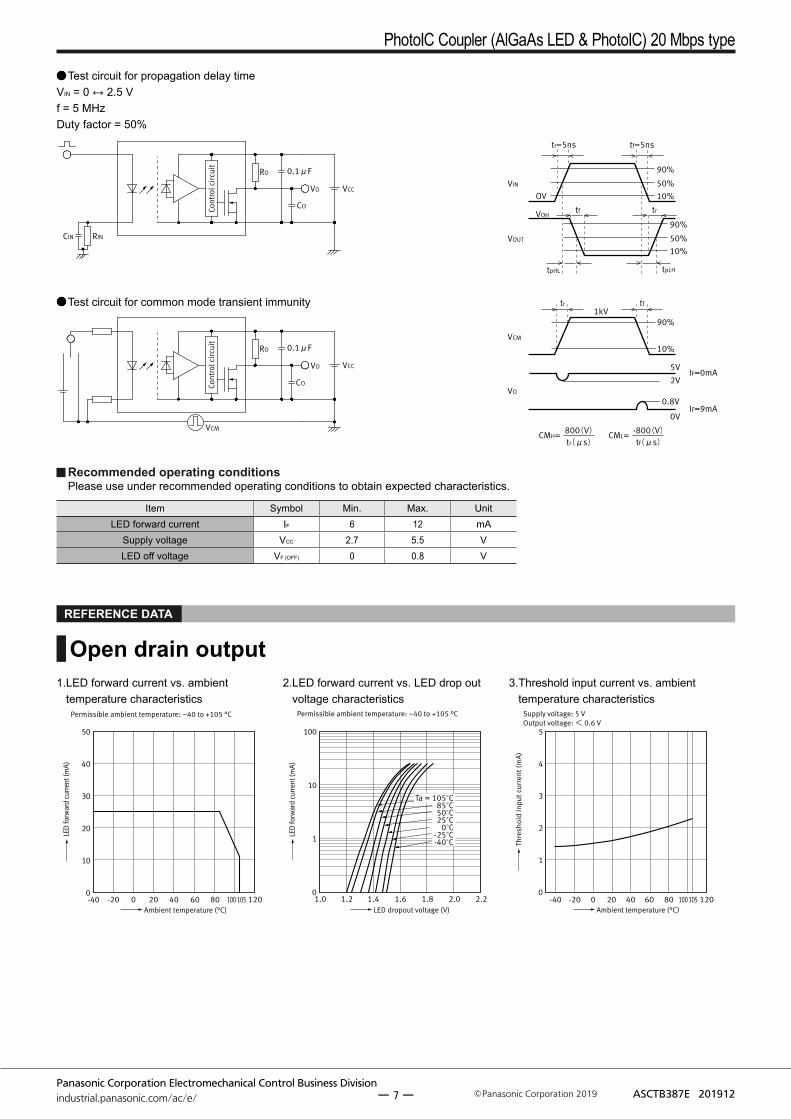
Recommended operating conditionsPlease use under recommended operating conditions to obtain expected characteristics.
Item Symbol Min. Max. UnitLED forward current IF 6 12 mA
Supply voltage VCC 2.7 5.5 VLED off voltage VF (OFF) 0 0.8 V
REFERENCE DATA
VCC
0.1μF
CO
CIN RIN
Cont
rol c
ircui
t
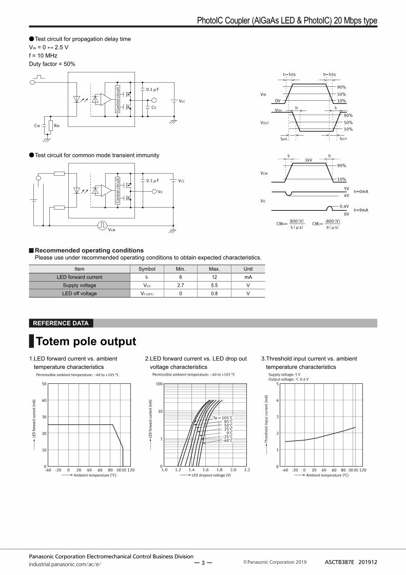
Test circuit for propagation delay timeVIN = 0 ↔ 2.5 Vf = 10 MHzDuty factor = 50%
VIN
VOUT
VOH
tr=5ns
tf tr
tf=5ns
tpLHtpHL
90%
50%10%
90%
50%10%
OV
VCC
VCM
0.1μF
VO
Cont
rol c
ircui
t
Test circuit for common mode transient immunity
VCM
VO
IF=0mA
IF=9mA
tftr
CMH= 800(V)tr(μs)
CML= -800(V)tf(μs)
90%
10%
1kV
5V4V
0.4V
0V
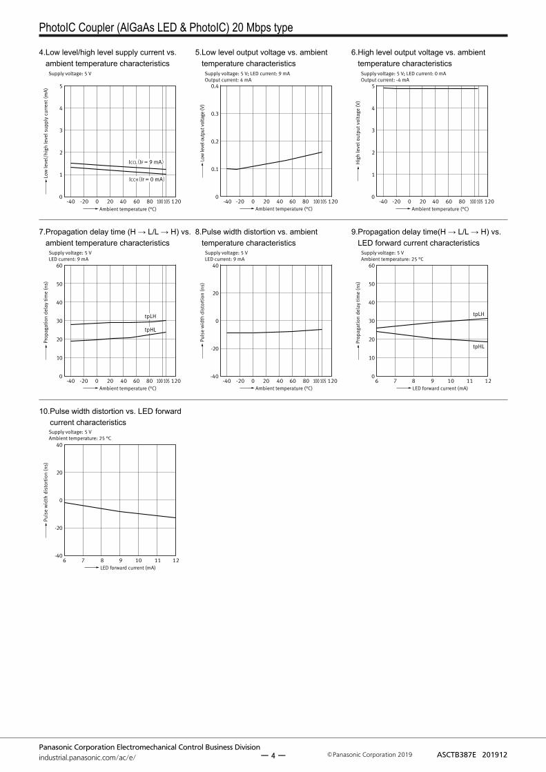
Totem pole output1. LED forward current vs. ambient
temperature characteristics
-400
20
10
30
40
50
-20 0 20 6040 80 100 105 120Ambient temperature (°C)
LED
forw
ard
curre
nt (m
A)
Permissible ambient temperature: –40 to +105 °C
2. LED forward current vs. LED drop outvoltage characteristics
1.00
1
10
100
1.2 1.4 1.6 1.8 2.0 2.2
Ta = 105°C85°C50°C25°C
0°C-25°C-40°C
LED dropout voltage (V)
LED
forw
ard
curre
nt (m
A)
Permissible ambient temperature: –40 to +105 °C
3. Threshold input current vs. ambienttemperature characteristics
-40 -20 0 20 6040 80 100 105 1200
1
2
3
4
5
Ambient temperature (°C)
Thre
shol
d in
put c
urre
nt (m
A)
Supply voltage: 5 VOutput voltage: < 0.4 V
ー 3 ー
PhotoIC Coupler (AlGaAs LED & PhotoIC) 20 Mbps type
Panasonic Corporation Electromechanical Control Business Divisionindustrial.panasonic.com/ac/e/ ASCTB387E 201912Panasonic Corporation 2019
4. Low level/high level supply current vs. ambient temperature characteristics
-400
2
1
3
4
5
-20 0 20 40 60 80 100 105 120
ICCL(IF = 9 mA)
ICCH(IF = 0 mA)
Ambient temperature (°C)
Low
leve
l/hi
gh le
vel s
uppl
y cu
rren
t (m
A)
Supply voltage: 5 V
5. Low level output voltage vs. ambient temperature characteristics
-400
0.1
0.2
0.3
0.4
-20 0 20 40 60 80 100 105 120Ambient temperature (°C)
Low
leve
l out
put v
olta
ge (V
)
Supply voltage: 5 V; LED current: 9 mAOutput current: 4 mA
6. High level output voltage vs. ambient temperature characteristics
-400
4
3
2
1
5
-20 0 20 40 60 80 100 105 120Ambient temperature (°C)
Hig
h le
vel o
utpu
t vol
tage
(V)
Supply voltage: 5 V; LED current: 0 mAOutput current: -4 mA
7. Propagation delay time (H → L/L → H) vs. ambient temperature characteristics
-400
20
10
30
40
50
60
-20 0 20 40 8060 100 105 120
tpLH
tpHL
Ambient temperature (°C)
Prop
agat
ion
dela
y tim
e (n
s)
Supply voltage: 5 VLED current: 9 mA
8. Pulse width distortion vs. ambient temperature characteristics
-40
0
-20
20
40
-40 -20 0 20 40 60 80 100 105 120Ambient temperature (°C)
Puls
e w
idth
dis
tort
ion
(ns)
Supply voltage: 5 VLED current: 9 mA
9. Propagation delay time(H → L/L → H) vs. LED forward current characteristics
60
30
20
10
40
50
60
7 8 9 10 1211
tpLH
tpHL
LED forward current (mA)
Prop
agat
ion
dela
y tim
e (n
s)
Supply voltage: 5 VAmbient temperature: 25 °C
10. Pulse width distortion vs. LED forward current characteristics
6
40
20
0
-20
-407 8 9 10 11 12
LED forward current (mA)
Puls
e w
idth
dis
tort
ion
(ns)
Supply voltage: 5 VAmbient temperature: 25 °C
ー 4 ー
PhotoIC Coupler (AlGaAs LED & PhotoIC) 20 Mbps type
Panasonic Corporation Electromechanical Control Business Divisionindustrial.panasonic.com/ac/e/ ASCTB387E 201912Panasonic Corporation 2019
Open drain outputAbsolute maximum ratings (Ambient temperature: 25°C)
Item Symbol APS2241S Remarks
Inpu
t
LED forward current IF 25 mALED reverse voltage VR 5 V
Peak forward current IFP 1 Af = 100 Hz, Duty Ratio = 0.1%1shot
Out
put
Supply voltage VCC 6 VOutput voltage V0 6 VOutput current I0 25 mAPower dissipation Pout 40 mW
I/O isolation voltage Viso 3,750 Vrms
Ambient temperature (Operating) Topr -40 to +105°C (Avoid icing and condensation)
Ambient temperature (Storage) Tstg -40 to +125°C
RATING
Electrical characteristics (Unless otherwise specified, Ta = -40 to +105°C, VCC = 2.7 to 5.5V)Item Symbol APS2241S Condition
Inpu
t
Threshold input current Maximum IFHL 4 mA VCC = 5 V
VO < 0.6 V
LED dropout voltage
MinimumVF
1.45 VIF = 10 mA Ta = 25°CTypical 1.6 V
Maximum 1.8 V
Input capacitance Typical Ct 20 pFf = 1 MHz VB = 0 VTa = 25°C
Out
put
Low level supplycurrent Maximum ICCL 3 mA IF = 9 mA
High level supplycurrent Maximum ICCH 3 mA IF = 0 mA
Low level output voltage Maximum VOL 0.6 V
IF = 9 mAIO = 13 mA VCC = 5 V
High level output current Maximum VOH 50 μA
IF = 0 mA VCC = 5.5 VVO = 5.5 V
ー 5 ー
PhotoIC Coupler (AlGaAs LED & PhotoIC) 20 Mbps type
Panasonic Corporation Electromechanical Control Business Divisionindustrial.panasonic.com/ac/e/ ASCTB387E 201912Panasonic Corporation 2019
IF
0.1μF A ICCL
VCC
Cont
rol c
ircui
t
Test circuit for ICCL
Item Symbol APS2241S Condition
Propagation delay time (H → L) Maximum tpHL 60 ns
VIN = 0→2.5 V, RIN = 100 Ω CIN = 15 pF, RO = 360 ΩCO = 15 pF
Propagation delay time (L → H) Maximum tpLH 60 ns
VIN = 2.5→0 V, RIN = 100 Ω CIN = 15 pF, RO = 360 ΩCO = 15 pF
Propagation delay skew Maximum tpsk 40 ns −
Pulse width distortion Maximum |tpHL-tpLH| 35 nsVIN = 2.5 V/5 MHz, RIN = 100 Ω CIN = 15 pF, RO = 360 ΩCO = 15 pF
Output fall time Typical tf 1 nsVIN = 0→2.5 V, RIN = 100 Ω CIN = 15 pF, RO = 360 ΩCO = 15 pF
Output rise time Typical tr 18 nsVIN = 2.5→0 V, RIN = 100 Ω CIN = 15 pF, RO = 360 ΩCO = 15 pF
Common mode transient immunity at low level output Minimum CML 20 kV/μs
VCM = 1000 Vp-p, IF = 9 mA VCC = 5 V, VO(MAX) = 0.8 V Ta = 25°C
Common mode transient immunity at high level output Minimum CMH 20 kV/μs
VCM = 1000 Vp-p, IF = 0 mA VCC = 5 V, VO(MIN) = 2 VTa = 25°C
I/O capacitance Typical Ciso 0.5 pF f = 1 MHz, VB = 0 VTa = 25°C
Initial I/O isolationresistance Minimum Riso 1,000 MΩ 500 V DC, RH ≦ 60%
Ta = 25°C
0.1μF A ICCH
VCC
Cont
rol c
ircui
t
Test circuit for ICCH
IOVIF
0.1μF
VCC
VOL
Cont
rol c
ircui
t
Test circuit for VOL
IOH
A0.1μF
VO
VCC
Cont
rol c
ircui
t
Test circuit for IOH
ー 6 ー
PhotoIC Coupler (AlGaAs LED & PhotoIC) 20 Mbps type
Panasonic Corporation Electromechanical Control Business Divisionindustrial.panasonic.com/ac/e/ ASCTB387E 201912Panasonic Corporation 2019
Recommended operating conditionsPlease use under recommended operating conditions to obtain expected characteristics.
Item Symbol Min. Max. UnitLED forward current IF 6 12 mA
Supply voltage VCC 2.7 5.5 VLED off voltage VF (OFF) 0 0.8 V
REFERENCE DATA
CO
VO
CIN RIN
RO 0.1μF
VCC
Cont
rol c
ircui
t
Test circuit for propagation delay timeVIN = 0 ↔ 2.5 Vf = 5 MHzDuty factor = 50%
VIN
VOUT
VOH
tr=5ns
tf tr
tf=5ns
tpLHtpHL
90%
50%10%
90%
50%10%
OV
VCM
VO
CO
RO
VCC
0.1μF
Cont
rol c
ircui
t
Test circuit for common mode transient immunity
VCM
VO
IF=0mA
IF=9mA
tftr
CMH= 800(V)tr(μs)
CML= -800(V)tf(μs)
90%
10%
1kV
5V2V
0.8V
0V
Open drain output1. LED forward current vs. ambient
temperature characteristics
-400
20
10
30
40
50
-20 0 20 6040 80 100 105 120Ambient temperature (°C)
LED
forw
ard
curre
nt (m
A)
Permissible ambient temperature: –40 to +105 °C
2. LED forward current vs. LED drop outvoltage characteristics
1.00
1
10
100
1.2 1.4 1.6 1.8 2.0 2.2
Ta = 105°C85°C50°C25°C
0°C-25°C-40°C
LED dropout voltage (V)
LED
forw
ard
curre
nt (m
A)
Permissible ambient temperature: –40 to +105 °C
3. Threshold input current vs. ambienttemperature characteristics
-40 -20 0 20 6040 80 100 105 1200
1
2
3
4
5
Ambient temperature (°C)
Thre
shol
d in
put c
urre
nt (m
A)
Supply voltage: 5 VOutput voltage: < 0.6 V
ー 7 ー
PhotoIC Coupler (AlGaAs LED & PhotoIC) 20 Mbps type
Panasonic Corporation Electromechanical Control Business Divisionindustrial.panasonic.com/ac/e/ ASCTB387E 201912Panasonic Corporation 2019
4.3±0.2
1.271.270.4
4.4±
0 .2
2 .1±
0 .2
0 .1
0.4Terminal thickness: t = 0.15
General tolerance: ±0.1
0.5
6 .8±
0 .4
0 .5
61 .
2
0.8
1.27
2.54
Tolerance: ±0.1
4. Low level/high level supply current vs. ambient temperature characteristics
-400
2
1
3
4
5
-20 0 20 40 60 80 100 105 120
ICCL(IF = 9 mA)
ICCH(IF = 0 mA)
Ambient temperature (°C)
Low
leve
l/hi
gh le
vel s
uppl
y cu
rren
t (m
A)
Supply voltage: 5 V
5. Low level output voltage vs. ambient temperature characteristics
-400
0.1
0.2
0.3
0.4
-20 0 20 40 60 80 100 105 120Ambient temperature (°C)
Low
leve
l out
put v
olta
ge (V
)
Supply voltage: 5 V; LED current: 9 mAOutput current: 13 mA
6. Propagation delay time (H → L/L → H) vs. ambient temperature characteristics
-400
20
10
30
40
50
60
-20 0 20 40 8060 100 105 120
tpLH
tpHL
Ambient temperature (°C)
Prop
agat
ion
dela
y tim
e (n
s)
Supply voltage: 5 VLED current: 9 mA
7. Pulse width distortion vs. ambient temperature characteristics
-40
0
-20
20
40
-40 -20 0 20 40 60 80 100 105 120Ambient temperature (°C)
Puls
e w
idth
dis
tort
ion
(ns)
Supply voltage: 5 VLED current: 9 mA
8. Propagation delay time(H → L/L → H) vs. LED forward current characteristics
60
30
20
10
40
50
60
7 8 9 10 1211
tpLH
tpHL
LED forward current (mA)
Prop
agat
ion
dela
y tim
e (n
s)
Supply voltage: 5 VAmbient temperature: 25 °C
9. Pulse width distortion vs. LED forward current characteristics
6-40
40
20
0
-20
7 8 9 10 11 12LED forward current (mA)
Puls
e w
idth
dis
tort
ion
(ns)
Supply voltage: 5 VAmbient temperature: 25 °C
CAD External dimensions
DIMENSIONS CAD The CAD data of the products with a “CAD” mark can be downloaded from our Website. Unit: mm
Recommended mounting pad(TOP VIEW)
Please refer to "the latest product specifications"when designing your product.•Requests to customers:https://industrial.panasonic.com/ac/e/salespolicies/
SAFETY STANDARDS
Part No.UL (Recognized) CSA (Certified)
RemarksFile No. (Standard No.) Contact rating File No.
(Standard No.) Contact rating
PhotoIC Coupler 20 Mbps
APS1241S E191218 (UL1577) - (Certified by C-UL)
APS2241S
Note: For the latest information on compliance with safety standards, please refer to our website.
ー 8 ー
Panasonic Corporation Electromechanical Control Business Divisionindustrial.panasonic.com/ac/e/ Panasonic Corporation 2020
PhotoMOS® Cautions for Use
SAFETY WARNINGS Do not use the product under conditions that exceed the range of its specifications. It may cause overheating, smoke, or fire. Do not touch the recharging unit while the power is on. There is a danger of electrical shock. Be sure to turn off the power when performing mounting, maintenance, or repair operations on the device (including connecting parts such as the terminal board and socket).
Check the wiring diagrams in the catalog and be sure to connect the terminals correctly. If the device is energized with short circuit or any wrong connection, it may cause unexpected malfunction, abnormal heat or fire.
Derating designDerating is a significant factor for reliable design and product life. Even if the conditions of use (temperature, current, voltage, etc.) of the product are within the absolute maximum ratings, reliability may be lowered remarkably when continuously used in high load conditions (high temperature, high humidity, high current, high voltage, etc.) Therefore, please derate sufficiently below the absolute maximum ratings and evaluate the device in the actual condition.Moreover, regardless of the application, if malfunctioning can be expected to pose high risk to human life or to property, or if products are used in equipment otherwise requiring high operational safety, in addition to designing double circuits, that is, incorporating features such as a protection circuit or a redundant circuit, safety testing should also be carried out.
Applying stress that exceeds the absolute maximum ratingIf the voltage or current value for any of the terminals exceeds the absolute maximum rating, internal elements will deteriorate because of the overvoltage or overcurrent. In extreme cases, wiring may melt, or silicon P/N junctions may be destroyed.Therefore, the circuit should be designed in such a way that the load never exceed the absolute maximum ratings, even momentarily.
Input voltage (for Voltage-sensitive type)For rising and dropping ratio of input voltage(dv/dt), maintain Min. 100mV/ms.
Oscillation circuit and control circuit (for TSON)The oscillation circuit and control circuit of product may be destroyed by external noise, surge, static electricity and so on.For noise effect to peripheral circuits when oscillation circuit operates, please implement safety measures on the system before use by verifying operation under the actual design.
Deterioration and destruction caused by discharge of static electricity (for TSON/RF C×R3/RF C×R5/RF C×R10)This phenomenon is generally called static electricity destruction, and occurs when static electricity generated by various factors is discharged while the PhotoMOS® terminals are in contact, producing internal destruction of the element.To prevent problems from static electricity, the following precautions and measures should be taken when using your device.1) Employees handling PhotoMOS® should wear anti-static clothing
and should be grounded through protective resistance of 500kΩto 1MΩ.
2) A conductive metal sheet should be placed over the worktable.Measuring instruments and jigs should be grounded.
3) When using soldering irons, either use irons with low leakagecurrent, or ground the tip of the soldering iron. (Use of low-voltagesoldering irons is also recommended.)
4) Devices and equipment used in assembly should also begrounded.
5) When packing printed circuit boards and equipment, avoid usinghigh-polymer materials such as foam styrene, plastic, and othermaterials which carry an electrostatic charge.
6) When storing or transporting PhotoMOS®, the environment shouldnot be conducive to generating static electricity (for instance, thehumidity should be between 45% and 60%), and PhotoMOS®
should be protected using conductive packing materials.
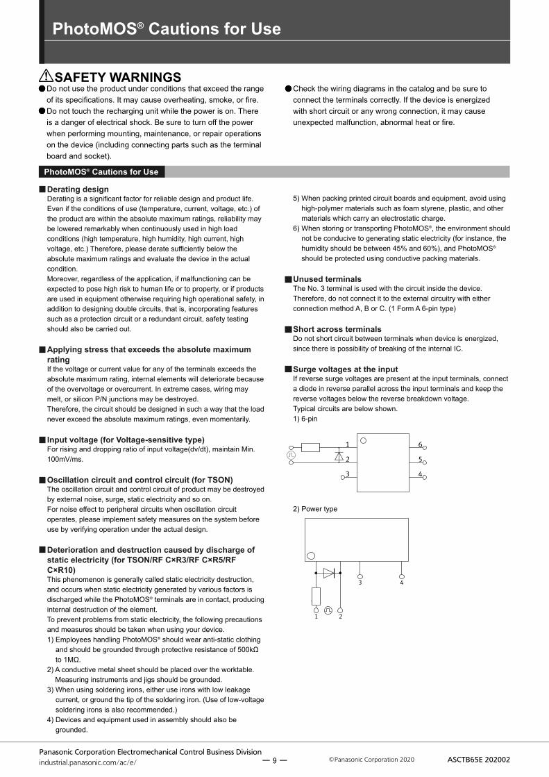
Unused terminalsThe No. 3 terminal is used with the circuit inside the device. Therefore, do not connect it to the external circuitry with either connection method A, B or C. (1 Form A 6-pin type)
Short across terminalsDo not short circuit between terminals when device is energized, since there is possibility of breaking of the internal IC.
Surge voltages at the inputIf reverse surge voltages are present at the input terminals, connect a diode in reverse parallel across the input terminals and keep the reverse voltages below the reverse breakdown voltage. Typical circuits are below shown.1) 6-pin
1
2
3
6
5
4
2) Power type
3
21
4
PhotoMOS® Cautions for Use
ASCTB65E 202002ー 9 ー
Panasonic Corporation Electromechanical Control Business Divisionindustrial.panasonic.com/ac/e/
PhotoMOS® Cautions for Use
Panasonic Corporation 2020
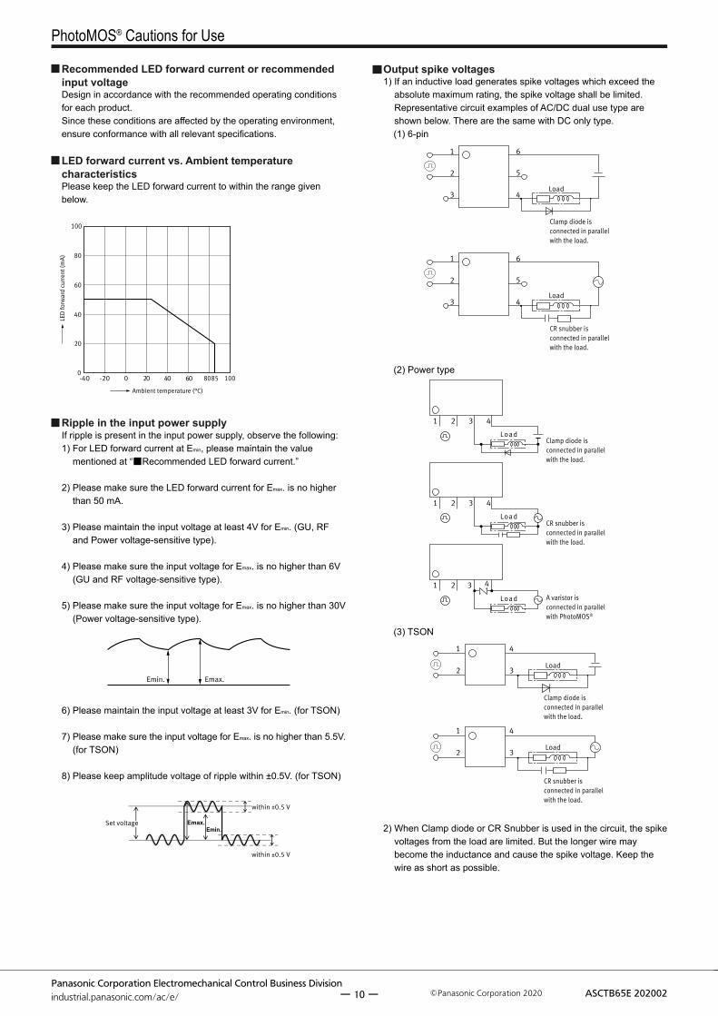
Recommended LED forward current or recommended input voltageDesign in accordance with the recommended operating conditions for each product.Since these conditions are affected by the operating environment, ensure conformance with all relevant specifications.
LED forward current vs. Ambient temperature characteristicsPlease keep the LED forward current to within the range given below.
0
20
40
100
80
60
0 20 40 60 8085 100-40 -20
Ambient temperature (°C)
LED
forw
ard
curr
ent (
mA)
Ripple in the input power supplyIf ripple is present in the input power supply, observe the following:1) For LED forward current at Emin, please maintain the value
mentioned at “■Recommended LED forward current.”
2) Please make sure the LED forward current for Emax. is no higherthan 50 mA.
3) Please maintain the input voltage at least 4V for Emin. (GU, RFand Power voltage-sensitive type).
4) Please make sure the input voltage for Emax. is no higher than 6V(GU and RF voltage-sensitive type).
5) Please make sure the input voltage for Emax. is no higher than 30V(Power voltage-sensitive type).
Emin. Emax.
6) Please maintain the input voltage at least 3V for Emin. (for TSON)
7) Please make sure the input voltage for Emax. is no higher than 5.5V.(for TSON)
8) Please keep amplitude voltage of ripple within ±0.5V. (for TSON)
within ±0.5 V
Set voltageSet voltage
within ±0.5 V
Output spike voltages1) If an inductive load generates spike voltages which exceed the
absolute maximum rating, the spike voltage shall be limited.Representative circuit examples of AC/DC dual use type areshown below. There are the same with DC only type.(1) 6-pin
1
2
3 4
1
2
3 4
5
5
6
6
Load
Load
Clamp diode isconnected in parallelwith the load.
CR snubber isconnected in parallelwith the load.
(2) Power type
1 2 3 4
1 2 3 4
1 2 3 4
Clamp diode isconnected in parallelwith the load.
Load
Load
Load
CR snubber isconnected in parallelwith the load.
A varistor isconnected in parallelwith PhotoMOS®
(3) TSON
1
2
4
3
1
2
4
3
Load
Load
Clamp diode isconnected in parallelwith the load.
CR snubber isconnected in parallelwith the load.
2) When Clamp diode or CR Snubber is used in the circuit, the spikevoltages from the load are limited. But the longer wire maybecome the inductance and cause the spike voltage. Keep thewire as short as possible.
ASCTB65E 202002ー 10 ー
PhotoMOS® Cautions for Use
Panasonic Corporation 2020
Reverse voltages at the input (for TSON)If reverse voltages are present at the input terminals, for example, connect a schottky barrier diode in reverse parallel across the input terminals and keep the reverse voltages below the reverse breakdown voltage. Typical circuit is shown below.
1
2
4
3
Continual DC bias (AQV259 and AQV258)If a continual DC bias will be applied between the input and output, the breakdown voltage of the switching element MOSFET on the output side may degrade. Therefore, be sure to test the product under actual conditions. Example of circuits that will cause degradation of breakdown voltage of MOSFET is given below.
IFIL
1
2
3
6
5
4
E
Load
Cleaning solvents compatibilityCleaning the solder flux should use the immersion washing with an organic solvent. If you have to use ultrasonic cleaning, please adopt the following conditions and check that there are no problems in the actual usage.• Frequency: 27 to 29kHz• Ultrasonic output: No greater than 0.25W/cm2*• Cleaning time: 30s or less• Cleanser used: Asahiklin AK-225• Others: Float PCB and the device in the cleaning solvent to
prevent from contacting the ultrasonic vibrator* Applies to unit area ultrasonic output for ultrasonic baths
Notes for mounting1) When different kinds of packages are mounted on PC boad,
temperature rise at soldering lead is highly dependent onpackage size. Therefore, please set the lower temperaturesoldering condition than the conditions of item “■Soldering”, andconfirm the temperature condition of actual usage beforesoldering.
2) When soldering condition exceeds our recommendation, thePhotoMOS® characteristics may be adversely affected. It mayoccur package crack or bonding wire breaking because ofthermal expansion unconformity and resin strength reduction.Please contact our sales office about the propriety of thecondition.
3) Please confirm the heat stress by using actual board because itmay be changed by board condition or manufacturing processcondition.
4) Solder creepage, wettability, or soldering strength will be affectedby the soldering condition or used soldering type. Please checkthem under the actual production condition in detail.
5) Please apply coating when the device returns to a roomtemperature.
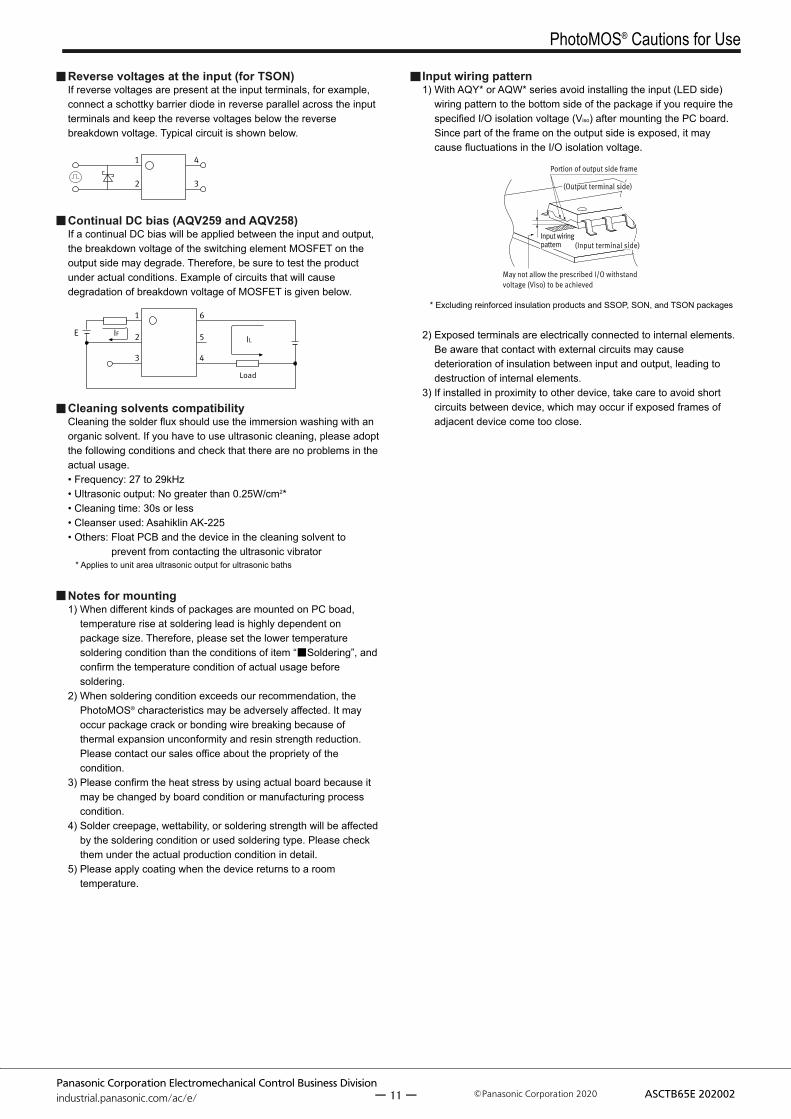
Input wiring pattern1) With AQY* or AQW* series avoid installing the input (LED side)
wiring pattern to the bottom side of the package if you require thespecified I/O isolation voltage (Viso) after mounting the PC board.Since part of the frame on the output side is exposed, it maycause fluctuations in the I/O isolation voltage.
(Output terminal side)(Output terminal side)
(Input terminal side)(Input terminal side)Input wiringpatternInput wiringpattern
May not allow the prescribed I/O withstandvoltage (Viso) to be achieved
Portion of output side framePortion of output side frame
* Excluding reinforced insulation products and SSOP, SON, and TSON packages
2) Exposed terminals are electrically connected to internal elements.Be aware that contact with external circuits may causedeterioration of insulation between input and output, leading todestruction of internal elements.
3) If installed in proximity to other device, take care to avoid shortcircuits between device, which may occur if exposed frames ofadjacent device come too close.
ASCTB65E 202002ー 11 ーPanasonic Corporation Electromechanical Control Business Divisionindustrial.panasonic.com/ac/e/
Panasonic Corporation Electromechanical Control Business Divisionindustrial.panasonic.com/ac/e/
PhotoMOS® Cautions for Use
Panasonic Corporation 2020
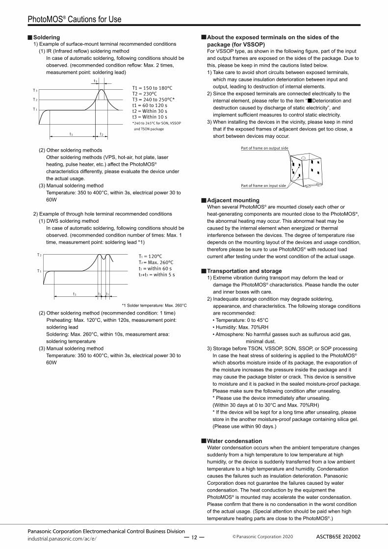
About the exposed terminals on the sides of the package (for VSSOP)For VSSOP type, as shown in the following figure, part of the input and output frames are exposed on the sides of the package. Due to this, please be keep in mind the cautions listed below.1) Take care to avoid short circuits between exposed terminals,
which may cause insulation deterioration between input and output, leading to destruction of internal elements.
2) Since the exposed terminals are connected electrically to theinternal element, please refer to the item “■Deterioration anddestruction caused by discharge of static electricity”, andimplement sufficient measures to control static electricity.
3) When installing the devices in the vicinity, please keep in mindthat if the exposed frames of adjacent devices get too close, ashort between devices may occur.
Part of frame on output side
Part of frame on input side
Adjacent mountingWhen several PhotoMOS® are mounted closely each other or heat-generating components are mounted close to the PhotoMOS®, the abnormal heating may occur. This abnormal heat may be caused by the internal element when energized or thermal interference between the devices. The degree of temperature rise depends on the mounting layout of the devices and usage condition, therefore please be sure to use PhotoMOS® with reduced load current after testing under the worst condition of the actual usage.
Transportation and storage1) Extreme vibration during transport may deform the lead or
damage the PhotoMOS® characteristics. Please handle the outerand inner boxes with care.
2) Inadequate storage condition may degrade soldering,appearance, and characteristics. The following storage conditionsare recommended:• Temperature: 0 to 45°C• Humidity: Max. 70%RH• Atmosphere: No harmful gasses such as sulfurous acid gas,
minimal dust.3) Storage before TSON, VSSOP, SON, SSOP, or SOP processing
In case the heat stress of soldering is applied to the PhotoMOS®
which absorbs moisture inside of its package, the evaporation ofthe moisture increases the pressure inside the package and itmay cause the package blister or crack. This device is sensitiveto moisture and it is packed in the sealed moisture-proof package.Please make sure the following condition after unsealing.* Please use the device immediately after unsealing.(Within 30 days at 0 to 30°C and Max. 70%RH)* If the device will be kept for a long time after unsealing, pleasestore in the another moisture-proof package containing silica gel.(Please use within 90 days.)
Water condensationWater condensation occurs when the ambient temperature changes suddenly from a high temperature to low temperature at high humidity, or the device is suddenly transferred from a low ambient temperature to a high temperature and humidity. Condensation causes the failures such as insulation deterioration. Panasonic Corporation does not guarantee the failures caused by water condensation. The heat conduction by the equipment the PhotoMOS® is mounted may accelerate the water condensation. Please confirm that there is no condensation in the worst condition of the actual usage. (Special attention should be paid when high temperature heating parts are close to the PhotoMOS®.)
Soldering1) Example of surface-mount terminal recommended conditions
(1) IR (Infrared reflow) soldering methodIn case of automatic soldering, following conditions should beobserved. (recommended condition reflow: Max. 2 times,measurement point: soldering lead)
t3
T 3
T 2
T 1
t2t1
T1 = 150 to 180°CT2 = 230°CT3 = 240 to 250°C*t1 = 60 to 120 st2 = Within 30 st3 = Within 10 s*240 to 245°C for SON, VSSOP
and TSON package
(2) Other soldering methodsOther soldering methods (VPS, hot-air, hot plate, laserheating, pulse heater, etc.) affect the PhotoMOS®
characteristics differently, please evaluate the device underthe actual usage.
(3) Manual soldering methodTemperature: 350 to 400°C, within 3s, electrical power 30 to60W
2) Example of through hole terminal recommended conditions(1) DWS soldering method
In case of automatic soldering, following conditions should beobserved. (recommended condition number of times: Max. 1time, measurement point: soldering lead *1)
t3t2t1
T 1
T 2 T1 = 120°CT2
= Max. 260°Ct1 = within 60 st2+t3 = within 5 s
*1 Solder temperature: Max. 260°C
(2) Other soldering method (recommended condition: 1 time)Preheating: Max. 120°C, within 120s, measurement point:soldering leadSoldering: Max. 260°C, within 10s, measurement area:soldering temperature
(3) Manual soldering methodTemperature: 350 to 400°C, within 3s, electrical power 30 to60W
ASCTB65E 202002ー 12 ー
PhotoMOS® Cautions for Use
Panasonic Corporation 2020
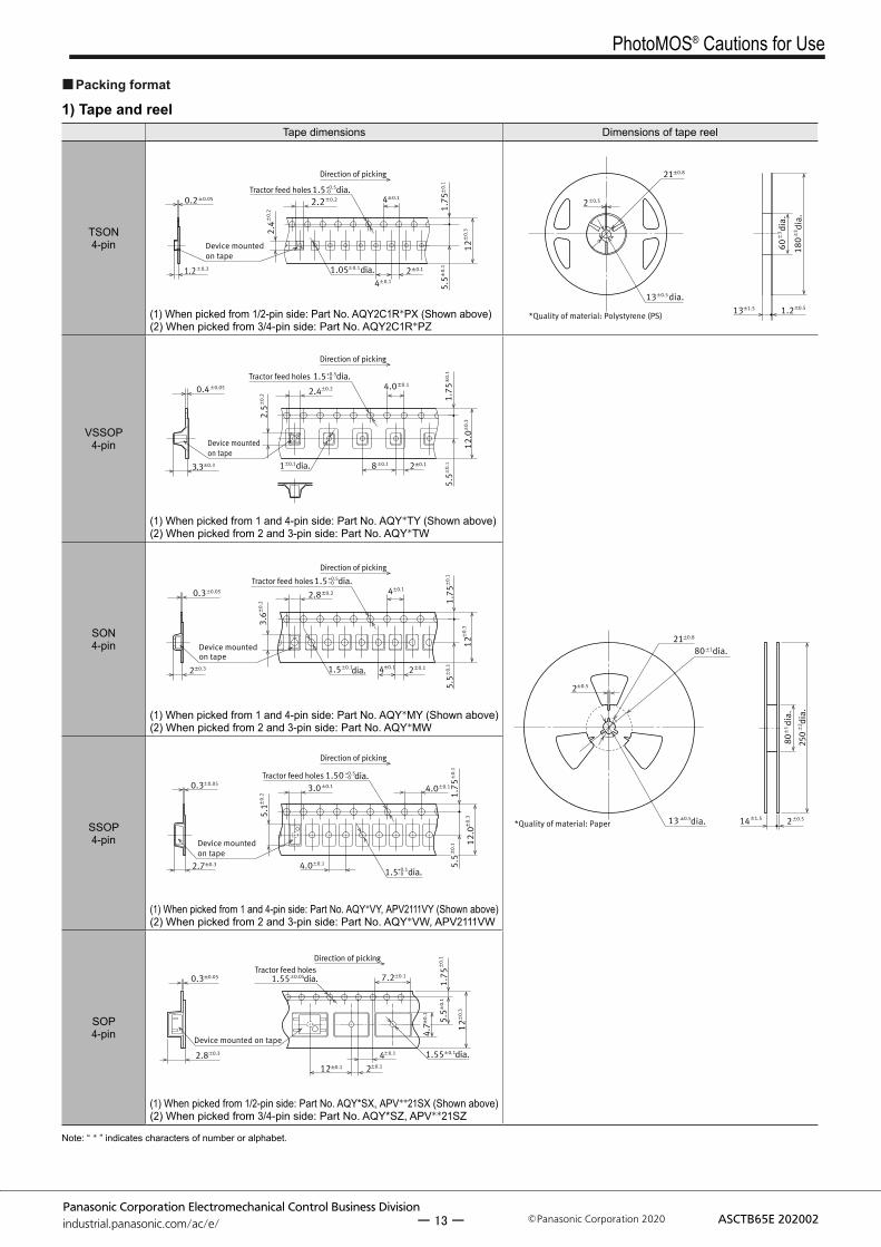
Packing format
1) Tape and reelTape dimensions Dimensions of tape reel
TSON4-pin
(1) When picked from 1/2-pin side: Part No. AQY2C1R*PX (Shown above)(2) When picked from 3/4-pin side: Part No. AQY2C1R*PZ
13±1.5 1.2±0.5
2±0.5
21±0.8
13±0.5dia.
60±
3 dia.
180±
3 dia.
*Quality of material: Polystyrene (PS)
VSSOP4-pin
(1) When picked from 1 and 4-pin side: Part No. AQY*TY (Shown above)(2) When picked from 2 and 3-pin side: Part No. AQY*TW
21±0.8
13±0.5 14±1.5 2±0.5
2±0.5
80±1
80±
1di
a.
250±
2 dia.
dia.
dia.
*Quality of material: Paper
SON4-pin
(1) When picked from 1 and 4-pin side: Part No. AQY*MY (Shown above)(2) When picked from 2 and 3-pin side: Part No. AQY*MW
SSOP4-pin
(1) When picked from 1 and 4-pin side: Part No. AQY*VY, APV2111VY (Shown above)(2) When picked from 2 and 3-pin side: Part No. AQY*VW, APV2111VW
SOP4-pin
(1) When picked from 1/2-pin side: Part No. AQY*SX, APV**21SX (Shown above)(2) When picked from 3/4-pin side: Part No. AQY*SZ, APV**21SZ
Note: “ * ” indicates characters of number or alphabet.
1.2±0.3
0.2±0.05
2.4±
0 .2
2.2±0.2
2±0.1
4
1.5+0.5-0
1.05
4±0.1
5.5±
0 .1
12±
0 .3
1 .75
±0 .
1
±0.1
±0.1dia.
dia.
Direction of picking
Device mountedon tape
Tractor feed holes
±0 .
11 .
754.0±0.11.5
0.4±0.05
3.3±0.3 1
2.4±0.2
8±0.1 2±0.1
±0 .
15 .
5
±0 .
312
.0
±0 .
22 .
5
±0.1
+0.5ー0
dia.
dia.
Direction of picking
Device mountedon tape
Tractor feed holes
0.3±0.05
2±0.3
±0 .
23 .
6
2.8±0.2 4±0.1
4±0.11.5±0.1
±0 .
11 .
75±
0 .1
5 .5
±0 .
312
2±0.1dia.
1.5 +0.5ー0 dia.
Direction of picking
Device mountedon tape
Tractor feed holes
0.3±0.05
2.7±0.3 4.0±0.1
3.0±0.1 4.0±0.1
±0 .
11 .
75±
0 .3
12.0
±0 .
15 .
5
±0 .
25 .
1
1.50 +0.5ー0
1.5+0.1ー0 dia.
dia.
Direction of picking
Device mountedon tape
Tractor feed holes
1.55±0.1
7.2 ±0.1
4 ±0.1
2±0.112 ±0.1
0.3±0.05
2.8 ±0.3
12±
0 .3
5 .5 ±
0 .1
1 .75
±0 .
1
4 .7 ±
0 .1
dia.
1.55±0.05dia.
Direction of picking
Device mounted on tape
Tractor feed holes
ASCTB65E 202002ー 13 ーPanasonic Corporation Electromechanical Control Business Divisionindustrial.panasonic.com/ac/e/
Panasonic Corporation Electromechanical Control Business Divisionindustrial.panasonic.com/ac/e/
PhotoMOS® Cautions for Use
Panasonic Corporation 2020
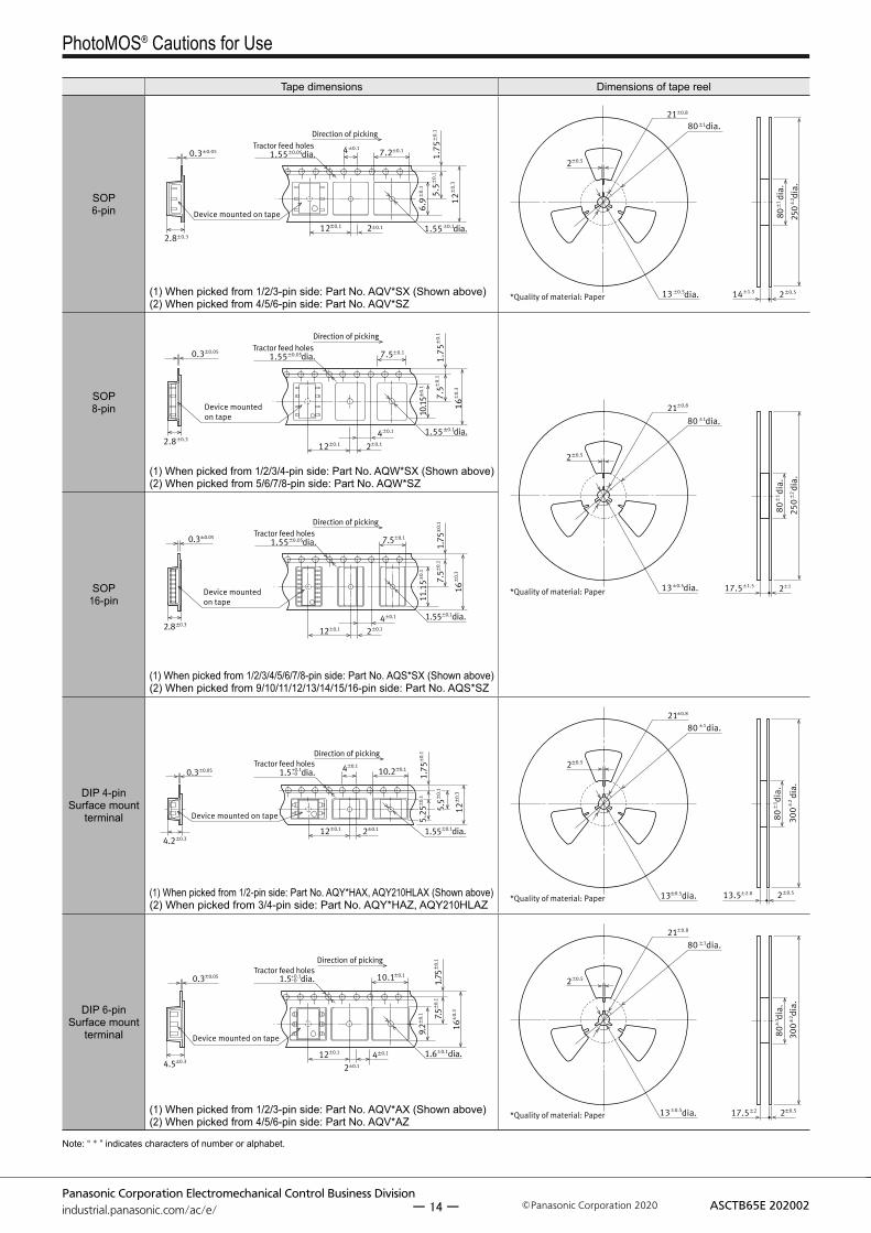
Tape dimensions Dimensions of tape reel
SOP6-pin
(1) When picked from 1/2/3-pin side: Part No. AQV*SX (Shown above)(2) When picked from 4/5/6-pin side: Part No. AQV*SZ
21±0.8
13±0.5 14±1.5 2±0.5
2±0.5
80±1
80±
1di
a.
250±
2 dia.
dia.
dia.
*Quality of material: Paper
SOP8-pin
(1) When picked from 1/2/3/4-pin side: Part No. AQW*SX (Shown above)(2) When picked from 5/6/7/8-pin side: Part No. AQW*SZ
21±0.8
13±0.5 17.5±1.5 2±1
2±0.5
80±1dia.
dia.
80±
1di
a.
250±
2di
a.
*Quality of material: PaperSOP16-pin
(1) When picked from 1/2/3/4/5/6/7/8-pin side: Part No. AQS*SX (Shown above)(2) When picked from 9/10/11/12/13/14/15/16-pin side: Part No. AQS*SZ
DIP 4-pinSurface mount
terminal
(1) When picked from 1/2-pin side: Part No. AQY*HAX, AQY210HLAX (Shown above)(2) When picked from 3/4-pin side: Part No. AQY*HAZ, AQY210HLAZ
21±0.8
13±0.5 13.5±2.0 2±0.5
2±0.5
80±1
dia.
80±
1 dia.
300±
2di
a.
dia.
*Quality of material: Paper
DIP 6-pinSurface mount
terminal
(1) When picked from 1/2/3-pin side: Part No. AQV*AX (Shown above)(2) When picked from 4/5/6-pin side: Part No. AQV*AZ
21±0.8
13±0.5 17.5±2 2±0.5
2±0.5
80±1
80±
1 dia.
dia.
dia.
300±
2 dia.
*Quality of material: Paper
Note: “ * ” indicates characters of number or alphabet.
1.55±0.1
7.2 ±0.14 ±0.1
2±0.112 ±0.1
0.3 ±0.05
2.8 ±0.3
12±
0 .3
5 .5 ±
0 .1
1 .75
±0 .
1
6 .9 ±
0 .1
dia.
1.55±0.05dia.
Direction of picking
Device mounted on tape
Tractor feed holes
7.5 ±0.1
4 ±0.1
2±0.112 ±0.1
0.3 ±0.05
2.8 ±0.3
16±
0 .3
7 .5 ±
0 .1
1 .75
±0 .
1
10.1
5 ±0 .
1
1.55±0.1dia.
1.55±0.05dia.
Direction of picking
Device mountedon tape
Tractor feed holes
1.55±0.1
7.5 ±0.1
4 ±0.1
2±0.112 ±0.1
0.3 ±0.05
2.8 ±0.3
16±
0 .3
7.5
±0.1
1 .75
±0 .
1
11.1
5 ±0 .
1
dia.
1.55±0.05dia.
Direction of picking
Device mountedon tape
Tractor feed holes
1.5
1.55±0.1
10.2 ±0.14 ±0.1
2±0.112 ±0.1
0.3 ±0.05
4.2 ±0.3
12±
0 .3
5 .5 ±
0 .1
1 .75
±0 .
15 .
25 ±0
.1
+0.1ー0 dia.
dia.
Direction of picking
Device mounted on tape
Tractor feed holes
1.6±0.1
10.1 ±0.1
4 ±0.1
2±0.1
12 ±0.1
0.3 ±0.05
4.5 ±0.3
16±
0 .3
7 .5 ±
0 .1
1 .75±
0 .1
9 .2 ±
0 .1
1.5+0.1ー0 dia.
dia.
Direction of picking
Device mounted on tape
Tractor feed holes
ASCTB65E 202002ー 14 ー
PhotoMOS® Cautions for Use
Panasonic Corporation 2020
Tape dimensions Dimensions of tape reel
DIP 8-pinSurface mount
terminal (Basic insulation
type)
(1) When picked from 1/2/3/4-pin side: Part No. AQW*AX (Shown above)(2) When picked from 5/6/7/8-pin side: Part No. AQW*AZ
21±0.8
13±0.5 17.5±2 2±0.5
2±0.5
80±1
80±
1 dia.
dia.
dia.
300±
2 dia.
*Quality of material: Paper
DIP 8-pinSurface mount
terminal(Reinforced
insulation type
(1) When picked from 1/2/3/4-pin side: Part No. AQW*EHAX, AQW210HLAX (Shown above)
(2) When picked from 5/6/7/8-pin side: Part No. AQW*EHAZ, AQW210HLAZ
Power-DIP4-pinSMD
(1) When picked from 1/2-pin side: Part No. AQY*AX (Shown above)(2) When picked from 3/4-pin side: Part No. AQY*AZ
21±0.8
13±0.5 25.5±2 1.7±0.8
2±0.5
100±1
dia.
dia.
100±
1 dia.
330±
2di
a.
*Quality of material: Paper
DIP 6-pinSurface mount
terminal(Photovoltaic
MOSFET driver)
(1) When picked from 1/2/3-pin side: Part No. APV1122AX (Shown above)(2) When picked from 4/6-pin side: Part No. APV1122AZ
21±0.8
13±0.5 17.5±2 2±0.5
2±0.5
80±1
80±
1 dia.
dia.
dia.
300±
2 dia.
*Quality of material: Paper
Note: “ * ” indicates characters of number or alphabet.
1.55±0.1
10.1 ±0.14 ±0.1
2±0.112 ±0.1
0.3 ±0.05
±0.3
16±
0 .3
7 .5 ±
0 .1
1 .75
±0 .
1
10.2
±0.1
4.5
1.5+0.1ー0 dia.
dia.
Direction of picking
Device mounted on tape
Tractor feed holes
1.5
1.55±0.1
10.2 ±0.14 ±0.1
2±0.112 ±0.1
0.3 ±0.05
4.2 ±0.3
16±
0 .3
7 .5 ±
0 .1
1 .75
±0 .
1
10.3
±0.1
+0.1ー0
dia.
dia.
Direction of picking
Device mounted on tape
Tractor feed holes
1.5
1.6±0.1
10.1 ±0.1
4 ±0.1
2±0.1
12 ±0.1
0.3 ±0.05
4.5 ±0.3
16±
0 .3
7 .5 ±
0 .1
1 .75
±0 .
1
9 .2 ±
0 .1
+0.1ー0
dia.
dia.
Direction of picking
Device mounted on tape
Tractor feed holes
1.55
1.55
4.0 ±0.1
16.0±0.1 2.0±0.1 ±0.1
12.6 ±0.1
1.75
±0.1
9 .7±
0 .1
11.5±
0 .1
24.0±
0 .3
0.3 ±0.05
4.5 ±0.3
+0.05ー0.05
dia.
dia.
Direction of picking
Device mountedon tape
Tractor feed holes
2) TubeDevices are packaged in a tube so that 1-pin is on the stopper Bside. Observe correct orientation when mounting them on PCboards.(PD type)
Stopper B Stopper A
(DIP type)Stopper A Stopper B
(SOP type)
Stopper B (green) Stopper A (gray)
(Power type)
GreenStopper B
GrayStopper A
ASCTB65E 202002ー 15 ーPanasonic Corporation Electromechanical Control Business Divisionindustrial.panasonic.com/ac/e/
Panasonic Corporation Electromechanical Control Business Divisionindustrial.panasonic.com/ac/e/
PhotoMOS® Cautions for Use
Panasonic Corporation 2020
Current limit function (output current control)1) Current limit function aims to increase resistance to surges when
the switch is turned on. Before using this function, connect the varistor to the output as shown in the figure below.
1
2
4
3
* Set the varistor voltage to 150 V or less.
Varistor Surge: 10×160μs 1.6kV
2) The current limit function capability can be lost if used longer than the specified time. Be sure to set the output loss to the Max. rate.
Short circuit protection circuitThe short circuit protection circuit is designed to protect circuits from excess current. Therefore, surge current may be detected as current overload in which case the output current will be cut and the off state maintained. For this reason, please include the inrush current in the load current and keep it below the maximum load current. Also, in order to maintain stability of internal IC operation, maintain an input current of at least 5 mA (Latch type), 10 mA (Non Latch type).
Photovoltaic MOSFET driver cautions for useWhen two external MOSFETs are connected with a common source terminal, oscillation may occur when operation is restored. Therefore, please insert a 100 to 1,000 Ω resistor between the gate terminal of the first MOSFET and the gate terminal of the second MOSFET.A typical example of this is given in the circuit below.
1
2
3 4
6
Input LED current (for Standard type) For rising and dropping ratio of input LED current (di/dt), maintain Min. 100 μA/s.
Input voltage (for Power voltage-sensitive type) For rising and dropping ratio of input voltage (dv/dt), maintain Min. 100 mV/s.
1) Power photoMOS® (1 Form A)
Absolute maximum rating Recommendedload voltageLoad voltage Load current
DC type
AQZ102 60 V DC 4.0 A DC 5, 12, 24 V DCAQZ105 100 V DC 2.6 A DC 48 V DCAQZ107 200 V DC 1.3 A DC 100 V DCAQZ104 400 V DC 0.7 A DC 200 V DC
AC/DC type
AQZ202 Peak AC, DC 60 V Peak AC, DC 3.0 A 12 V AC5, 12, 24 V DC
AQZ205 Peak AC, DC 100 V Peak AC, DC 2.0 A 24 V AC48 V DC
AQZ207 Peak AC, DC 200 V Peak AC, DC 1.0 A 48 V AC100 V DC
AQZ204 Peak AC, DC 400 V Peak AC, DC 0.5 A 120 V AC200 V DC
2) Power photoMOS® (1 Form B)
Absolute maximum rating Recommendedload voltageLoad voltage Load current
AC/DC type
AQZ404 Peak AC, DC 400 V Peak AC, DC 0.5 A 100 V AC200 V DC
3) Power photoMOS® Voltage-sensitive type (1 Form A)
Absolute maximum rating Recommendedload voltageLoad voltage Load current
DC type
AQZ102D 60 V DC 3.6 A DC 5, 12, 24 V DCAQZ105D 100 V DC 2.3 A DC 48 V DCAQZ107D 200 V DC 1.1 A DC 100 V DCAQZ104D 400 V DC 0.6 A DC 200 V DC
AC/DC type
AQZ202D Peak AC, DC 60 V Peak AC, DC 2.7 A 12 V AC5, 12, 24 V DC
AQZ205D Peak AC, DC 100 V Peak AC, DC 1.8 A 24 V AC48 V DC
AQZ207D Peak AC, DC 200 V Peak AC, DC 0.9 A 48 V AC100 V DC
AQZ204D Peak AC, DC 400 V Peak AC, DC 0.45 A 120 V AC200 V DC
4) Power photoMOS® High Capacity type (1 Form A)
Absolute maximum rating Recommendedload voltageLoad voltage Load current
DC type
AQZ192 60 V DC 10 A DC 5, 12, 24 V DCAQZ197 200 V DC 5 A DC 100 V DC
AC/DC type
AQZ202G Peak AC, DC 60 V Peak AC, DC 6 A 12 V AC5, 12, 24 V DC
AQZ205G Peak AC, DC 100 V Peak AC, DC 4 A 24 V AC48 V DC
AQZ207G Peak AC, DC 200 V Peak AC, DC 2 A 48 V AC100 V DC
AQZ206G2 Peak AC, DC 600 V Peak AC, DC 1 A 120, 240 V AC200, 400 V DC
Adjacent mounting (for Power type) 1) When devices are mounted close together with the heat-
generated devices, ambient temperature may rise abnormally. Mounting layout and ventilation should be considered.
2) When many devices are mounted close together, load current should be reduced. (Refer to the data of “Load current in adjacent mounting vs. Ambient temperature characteristics.”)
Recommended load voltageAs a guide in selecting PhotoMOS®, please refer to the following table.
ASCTB65E 202002ー 16 ー

Please contact ..........
Electromechanical Control Business Division
industral.panasonic.com/ac/e/
Specifications are subject to change without notice.
1006, Oaza Kadoma, Kadoma-shi, Osaka 571-8506, Japan
©Panasonic Corporation 2020
ASCTB387E 202002