Embed Size (px)
Citation preview

Photonic Crystals and Negative Refraction
Dane Wheeler
Jing Zhang

Introduction
Photonic crystals are materials with a periodic dielectric constant in one, two, or three dimensions
Like semiconductors with a periodic potential, photonic crystals exhibit a band gap
1 2 1 2 1 2 1 2 1 2 1 2
(x) = (x+a)a
2-D
periodic intwo directions
3-D
periodic inthree di rections
1-D
periodic inone direction
Johnson, S. G., “Photonic Crystals: Periodic Surprises in Electromagnetism”

Motivation
Perfect waveguide bendsPerfect channel-drop filtersNegative refraction
Perfect lens/lithography
Resonant cavitiesOptical logic
All-optical transistors
Yokohama National University/Baba Research Lab

Origin of Photonic Band Gap
E 1
c
t
H i
c
H
H
1
c
t
E
J i
c
E
1
H
c
2 H
eigen-operator
Faraday’s Law
Ampere’s Law
eigenvalue
Schrödinger-likeMaxwell equation
eigen-state

Photonic Band Structure
Solution leads to photonic band structure
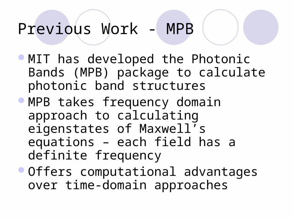
Previous Work - MPB
MIT has developed the Photonic Bands (MPB) package to calculate photonic band structures
MPB takes frequency domain approach to calculating eigenstates of Maxwell’s equations – each field has a definite frequency
Offers computational advantages over time-domain approaches

Previous Work – Negative Refraction
Cubukcu, et al. have experimentally demonstrated negative refraction by a photonic crystal
Structure is a square array of alumina rods in the air
Cubukcu, et al., Nature 423, 604-605 (2003).

3D Structures – Inverse Opal
Y. A. Vlasov, et al., Nature 414, 289-293 (2001).
Self-assembled silica opals grown on silicon substrate
LPCVD is used to fill opal template with silicon; wet
etching yields inverse opal silicon structure

3D Structures – Wire Mesh
Copper wire diamond mesh structure
Exhibits microwave band gap
Also exhibits cutoff frequency around 6-7 GHz
Able to produce large crystals – 18 x 18 x 7 cm (1 cm bonds)
D. F. Sievenpiper, et al., Phys. Rev. Lett. 76, 2480–2483 (1996).

3D PhC based on etched DBR
X-Y plane: Triangular array of holes
Z direction: Distributed Bragg Reflectors (DBR)
Materials: GaAs (1 = 14.44 )
and oxidized AlAs (2 = 2.25)
for large contrst.
Dimension Data: R/a is 0.275 and l1 / l2 is 1.69 for a
common band gap.
QuickTime™ and aTIFF (Uncompressed) decompressor
are needed to see this picture.

Computation methods for band structures
Plane Wave Expansion (PWE): Modified Maxwell’s Equation
H field expanded in plane waves
Eigen function to obtain band structure
FDTD: Finite Difference Time Domain
Electro-magnetic fields calculated at a given
instant in time

Calculated band structure with PWE method

Computation with MPB program for same structure

Refractive index calculated from Band Structure
Central Dilemma: d/d|k| < 0
Vg · k < 0 as Vg = ∂ / ∂k
Left Handed Material: E H · k < 0 E H: Poynting Vector, describing the magnitude and direction of the flow of energy.
Refractive Index: n = sign(Vg · k) c |k| /

Frequency contour in k space
Central Dilemma:
Convergent frequency contour in k space
gives negative refractive index.

Refractive index and corresponding band structure

Summary
Photonic crystals modulate light by modulating periodic structure and consequently photonic band diagram.
Advantages of photonic crystals: - Can be fabricated with wide range of materials. - Structure possibilities are limited only by human
imagination Wide applications Novel 3D photonic crystal structure can exhibit
overlapping band gaps along main crystal axes. Negative refractive index exists within certain frequency
range.