Embed Size (px)
Citation preview

Physical Principlesof Electron Microscopy
生物秀-专心做生物!
www.bbioo.cm

Ray F. Egerton
Physical Principlesof Electron MicroscopyAn Introduction to TEM, SEM, and AEM
With 122 Figures

Ray F. EgertonDepartment of Physics, University of Alberta412 Avadh Bhatia Physics LaboratoryEdmonton, Alberta, CanadaT6G 2R3
Library of Congress Control Number: 2005924717
ISBN-10: 0-387-25800-0 Printed on acid-free paper.ISBN-13: 978-0387-25800-0
© 2005 Springer Science+Business Media, Inc.All rights reserved. This work may not be translated or copied in whole or in part without the writtenpermission of the publisher (Springer Science+Business Media, Inc., 233 Spring St., New York, NY10013, USA), except for brief excerpts in connection with reviews or scholarly analysis. Use in connec-tion with any form of information storage and retrieval, electronic adaptation, computer software, or bysimilar or dissimilar methodology now known or hereafter developed is forbidden.The use in this publication of trade names, trademarks, service marks, and similar terms, even if they arenot identified as such, is not to be taken as an expression of opinion as to whether or not they are subjectto proprietary rights.
Printed in the United States of America. (EB)
9 8 7 6 5 4 3 2 1
springeronline.com

To Maia
Contents
Preface xi
1. An Introduction to Microscopy 1 1.1 Limitations of the Human Eye 21.2 The Light-Optical Microscope 51.3 The X-ray Microscope 91.4 The Transmission Electron Microscope 11 1.5 The Scanning Electron Microscope 17 1.6 Scanning Transmission Electron Microscope 19 1.7 Analytical Electron Microscopy 21 1.8 Scanning-Probe Microscopes 21
2. Electron Optics 272.1 Properties of an Ideal Image 272.2 Imaging in Light Optics 302.3 Imaging with Electrons 342.4 Focusing Properties of a Thin Magnetic Lens 41 2.5 Comparison of Magnetic and Electrostatic Lenses 432.6 Defects of Electron Lenses 44
3. The Transmission Electron Microscope 573.1 The Electron Gun 583.2 Electron Acceleration 67
viii Contents
3.3 Condenser-Lens System 70 3.4 The Specimen Stage 75 3.5 TEM Imaging System 78 3.6 Vacuum System 88
4. TEM Specimens and Images 934.1 Kinematics of Scattering by an Atomic Nucleus 94 4.2 Electron-Electron Scattering 96 4.3 The Dynamics of Scattering 97 4.4 Scattering Contrast from Amorphous Specimens 101 4.5 Diffraction Contrast from Polycrystalline Specimens 106 4.6 Dark-Field Images 108 4.7 Electron-Diffraction Patterns 108 4.8 Diffraction Contrast within a Single Crystal 112 4.9 Phase Contrast in the TEM 115 4.10 TEM Specimen Preparation 119
5. The Scanning Electron Microscope 1255.1 Operating Principle of the SEM 125 5.2 Penetration of Electrons into a Solid 129 5.3 Secondary-Electron Images 131 5.4 Backscattered-Electron Images 137 5.5 Other SEM Imaging Modes 139 5.6 SEM Operating Conditions 143 5.7 SEM Specimen Preparation 147 5.8 The Environmental SEM 149 5.9 Electron-Beam Lithography 151
6. Analytical Electron Microscopy 1556.1 The Bohr Model of the Atom 155 6.2 X-ray Emission Spectroscopy 158 6.3 X-Ray Energy-Dispersive Spectroscopy 161 6.4 Quantitative Analysis in the TEM 165 6.5 Quantitative Analysis in the SEM 167 6.6 X-Ray Wavelength-Dispersive Spectroscopy 167 6.7 Comparison of XEDS and XWDS Analysis 169 6.8 Auger Electron Spectroscopy 171 6.9 Electron Energy-Loss Spectroscopy 172

Contents ix
7. Recent Developments 1777.1 Scanning Transmission Electron Microscopy 177 7.2 Aberration Correction 180 7.3 Electron-Beam Monochromators 182 7.4 Electron Holography 184 7.5 Time-Resolved Microscopy 188
Appendix: Mathematical Derivations 191A.1 The Schottky Effect 191 A.2 Impact Parameter in Rutherford Scattering 193
References 195
Index 197
PREFACE
The telescope transformed our view of the universe, leading to cosmologicaltheories that derive support from experiments involving elementary particles.But microscopes have been equally important, by helping us to understandboth inanimate matter and living objects at their elementary level. Initially,these instruments relied on the focusing of visible light, but within the past50 years other forms of radiation have been used. Of these, electrons have arguably been the most successful, by providing us with direct images down to the atomic level.
The purpose of this book is to introduce concepts of electron microscopyand to explain some of the basic physics involved at an undergraduate level. It originates from a one-semester course at the University of Alberta,designed to show how the principles of electricity and magnetism, optics andmodern physics (learned in first or second year) have been used to develop instruments that have wide application in science, medicine and engineering.Finding a textbook for the course has always been a problem; most electron microscopy books overwhelm a non-specialist student, or else theyconcentrate on practical skills rather than fundamental principles. Over the years, this course became one of the most popular of our “general interest”courses offered to non-honors students. It would be nice to think that theavailability of this book might facilitate the introduction of similar courses atother institutions.
At the time of writing, electron microscopy is being used routinely in thesemiconductor industry to examine devices of sub-micrometer dimensions.Nanotechnology also makes use of electron beams, both for characterizationand fabrication. Perhaps a book on the basics of TEM and SEM will benefit the engineers and scientists who use these tools. The more advanced student or professional electron microscopist is already well served by existing
Prefacexii
textbooks, such as Williams and Carter (1996) and the excellent Springerbooks by Reimer. Even so, I hope that some of my research colleagues mayfind the current book to be a useful supplement to their collection.
My aim has been to teach general concepts, such as how a magnetic lens focuses electrons, without getting into too much detail as would be neededto actually design a magnetic lens. Because electron microscopy is interdisciplinary, both in technique and application, the physical principlesbeing discussed involve not only physics but also aspects of chemistry,electronics, and spectroscopy. I have included a short final chapter outliningsome recent or more advanced techniques, to illustrate the fact that electronmicroscopy is a “living” subject that is still undergoing development.
Although the text contains equations, the mathematics is restricted tosimple algebra, trigonometry, and calculus. SI units are utilized throughout.I have used italics for emphasis and bold characters to mark technical termswhen they first appear. On a philosophical note: although wave mechanics has proved invaluable for accurately calculating the properties of electrons,classical physics provides a more intuitive description at an elementary level. Except with regard to diffraction effects, I have assumed the electron to be a particle, even when treating “phase contrast” images. I hope Einstein would approve.
To reduce publishing costs, the manuscript was prepared as camera-readycopy. I am indebted to several colleagues for proofreading and suggestingchanges to the text; in particular, Drs. Marek Malac, Al Meldrum, RobertWolkow, and Rodney Herring, and graduate students Julie Qian, Peng Li,and Feng Wang.
Ray Egerton
University of Alberta Edmonton, Canada [email protected]
January 2005
Chapter 1
AN INTRODUCTION TO MICROSCOPY
Microscopy involves the study of objects that are too small to be examinedby the unaided eye. In the SI (metric) system of units, the sizes of theseobjects are expressed in terms of sub-multiples of the meter, such as themicrometer (1 m = 10-6 m, also called a micron) and also the nanometer
(1 nm = 10-9 m). Older books use the Angstrom unit (1 Å = 10-10 m), not an official SI unit but convenient for specifying the distance between atoms in a olid, which is generally in the range 2 3 Å.s
To describe the wavelength of fast-moving electrons or their behavior inside an atom, we need even smaller units. Later in this book, we will makese of the picometer (1 pm = 10-12 m).u
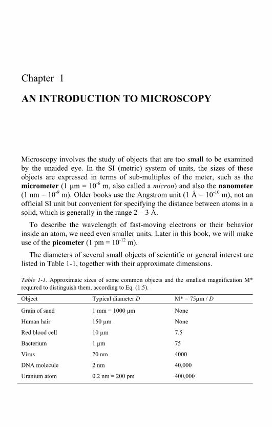
The diameters of several small objects of scientific or general interest arelisted in Table 1-1, together with their approximate dimensions.
Table 1-1. Approximate sizes of some common objects and the smallest magnification M*required to distinguish them, according to Eq. (1.5).
Object Typical diameter D M* = 75 m / D
Grain of sand 1 mm = 1000 µm None
Human hair 150 µm None
Red blood cell 10 µm 7.5
Bacterium 1 µm 75
Virus 20 nm 4000
DNA molecule 2 nm 40,000
Uranium atom 0.2 nm = 200 pm 400,000
Chapter 12
1.1 Limitations of the Human Eye
Our concepts of the physical world are largely determined by what we see
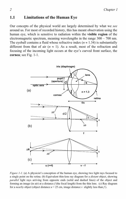
around us. For most of recorded history, this has meant observation using the human eye, which is sensitive to radiation within the visible region of the electromagnetic spectrum, meaning wavelengths in the range 300 – 700 nm.The eyeball contains a fluid whose refractive index (n 1.34) is substantially different from that of air (n 1). As a result, most of the refraction and focusing of the incoming light occurs at the eye’s curved front surface, thecornea; see Fig. 1-1.
pupil(aperture)
iris (diaphragm)
cornea
retina
n = 1.3
u (>>f) v f
(a)
(b)
(c)
f
R
lens
optic axisd
d/2
f/n
Figure 1-1. (a) A physicist’s conception of the human eye, showing two light rays focused toa single point on the retina. (b) Equivalent thin-lens ray diagram for a distant object, showingparallel light rays arriving from opposite ends (solid and dashed lines) of the object andforming an image (in air) at a distance f (the focal length) from the thin lens. (c) Ray diagramfor a nearby object (object distance u = 25 cm, image distance v slightly less than f ).
An Introduction to Microscopy 3
In order to focus on objects located at different distances (referred to asaccommodation), the eye incorporates an elastically deformable lens of slightly higher refractive index (n ~ 1.44) whose shape and focusing powerare controlled by eye muscles. Together, the cornea and lens of the eyebehave like a single glass lens of variable focal length, forming a real image
on the curved retina at the back of the eyeball. The retina contains photosensitive receptor cells that send electrochemical signals to the brain, the strength of each signal representing the local intensity in the image.However, the photochemical processes in the receptor cells work over alimited range of image intensity, therefore the eye controls the amount of light reaching the retina by varying the diameter d (over a range 2 8 mm)of the aperture of the eye, also known as the pupil. This aperture takes the form of a circular hole in the diaphragm (or iris), an opaque disk located
etween the lens and the cornea, as shown in Fig. 1-1.b
The spatial resolution of the retinal image, which determines how small
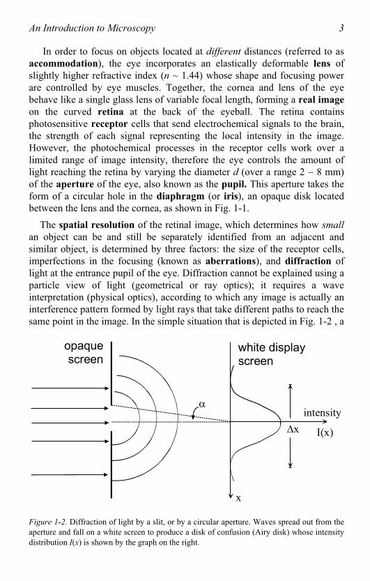
an object can be and still be separately identified from an adjacent and similar object, is determined by three factors: the size of the receptor cells, imperfections in the focusing (known as aberrations), and diffraction oflight at the entrance pupil of the eye. Diffraction cannot be explained using aparticle view of light (geometrical or ray optics); it requires a wave interpretation (physical optics), according to which any image is actually aninterference pattern formed by light rays that take different paths to reach thesame point in the image. In the simple situation that is depicted in Fig. 1-2 , a
x
opaquescreen
white displayscreen
intensity
x I(x)
Figure 1-2. Diffraction of light by a slit, or by a circular aperture. Waves spread out from theaperture and fall on a white screen to produce a disk of confusion (Airy disk) whose intensity distribution I(x) is shown by the graph on the right.
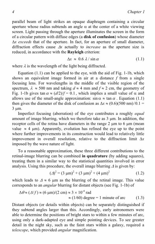
Chapter 14
parallel beam of light strikes an opaque diaphragm containing a circular aperture whose radius subtends an angle at the center of a white viewing screen. Light passing through the aperture illuminates the screen in the formof a circular pattern with diffuse edges (a disk of confusion) whose diameter
x exceeds that of the aperture. In fact, for an aperture of small diameter,diffraction effects cause x actually to increase as the aperture size isreduced, in accordance with the Rayleigh criterion:
x 0.6 / sin (1.1)
where is the wavelength of the light being diffracted.
Equation (1.1) can be applied to the eye, with the aid of Fig. 1-1b, whichshows an equivalent image formed in air at a distance f from a singlefocusing lens. For wavelengths in the middle of the visible region of thespectrum, 500 nm and taking d 4 mm and f 2 cm, the geometry of Fig. 1-1b gives tan (d/2)/f = 0.1 , which implies a small value of and allows use of the small-angle approximation: sin tan . Equation (1.1)then gives the diameter of the disk of confusion as x (0.6)(500 nm)/0.1 = 3 m.
Imperfect focusing (aberration) of the eye contributes a roughly equal
amount of image blurring, which we therefore take as 3 m. In addition, thereceptor cells of the retina have diameters in the range 2 m to 6 m (meanvalue 4 m). Apparently, evolution has refined the eye up to the pointwhere further improvements in its construction would lead to relatively little improvement in overall resolution, relative to the diffraction limit x
imposed by the wave nature of light.
To a reasonable approximation, these three different contributions to theretinal-image blurring can be combined in quadrature (by adding squares), treating them in a similar way to the statistical quantities involved in error analysis. Using this procedure, the overall image blurring is given by:
( )2 = (3 m)2 + (3 m)2 + (4 m)2 (1.2)
which leads to 6 m as the blurring of the retinal image. This value corresponds to an angular blurring for distant objects (see Fig. 1-1b) of
( / f ) (6 m)/(2 cm) 3 10-4 rad (1/60) degree = 1 minute of arc (1.3)
Distant objects (or details within objects) can be separately distinguished if they subtend angles larger than this. Accordingly, early astronomers wereable to determine the positions of bright stars to within a few minutes of arc,using only a dark-adapted eye and simple pointing devices. To see greaterdetail in the night sky, such as the faint stars within a galaxy, required atelescope, which provided angular magnification.
An Introduction to Microscopy 5
Changing the shape of the lens in an adult eye alters its overall focal length by only about 10%, so the closest object distance for a focused imageon the retina is u 25 cm. At this distance, an angular resolution of 3 10-4
rad corresponds (see Fig. 1c) to a lateral dimension of:
R ( ) u 0.075 mm = 75 m (1.4)
Because u 25 cm is the smallest object distance for clear vision, R = 75m can be taken as the diameter of the smallest object that can be resolved
(distinguished from neighboring objects) by the unaided eye, known as its object resolution or the spatial resolution in the object plane.
Because there are many interesting objects below this size, including theexamples in Table 1-1, an optical device with magnification factor M ( > 1) is needed to see them; in other words, a microscope.
To resolve a small object of diameter D, we need a magnification M* suchthat the magnified diameter (M* D) at the eye's object plane is greater or equal to the object resolution R ( 75 m) of the eye. In other words:
M* = ( R)/D (1.5)
Values of this minimum magnification are given in the right-hand column ofTable 1-1, for objects of various diameter D.
1.2 The Light-Optical Microscope
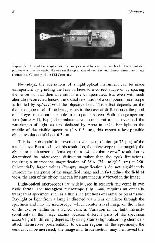
Light microscopes were developed in the early 1600’s, and some of thebest observations were made by Anton van Leeuwenhoek, using tiny glass lenses placed very close to the object and to the eye; see Fig. 1-3. By the late 1600’s, this Dutch scientist had observed blood cells, bacteria, and structure within the cells of animal tissue, all revelations at the time. But this simpleone-lens device had to be positioned very accurately, making observation ver tiring in practice.y
For routine use, it is more convenient to have a compound microscope,containing at least two lenses: an objective (placed close to the object to be magnified) and an eyepiece (placed fairly close to the eye). By increasing itsdimensions or by employing a larger number of lenses, the magnification M
of a compound microscope can be increased indefinitely. However, a large value of M does not guarantee that objects of vanishingly small diameter D
can be visualized; in addition to satisfying Eq. (1-5), we must ensure thataberrations and diffraction within the microscope are sufficiently low.
Chapter 16
Figure 1-3. One of the single-lens microscopes used by van Leeuwenhoek. The adjustablepointer was used to center the eye on the optic axis of the lens and thereby minimize imageaberrations. Courtesy of the FEI Company.
Nowadays, the aberrations of a light-optical instrument can be madeunimportant by grinding the lens surfaces to a correct shape or by spacing the lenses so that their aberrations are compensated. But even with such aberration-corrected lenses, the spatial resolution of a compound microscope is limited by diffraction at the objective lens. This effect depends on the diameter (aperture) of the lens, just as in the case of diffraction at the pupil of the eye or at a circular hole in an opaque screen. With a large-aperturelens (sin 1), Eq. (1.1) predicts a resolution limit of just over half the wavelength of light, as first deduced by Abbé in 1873. For light in themiddle of the visible spectrum ( 0.5 m), this means a best-possibleobject resolution of about 0.3 m.
This is a substantial improvement over the resolution ( 75 m) of the unaided eye. But to achieve this resolution, the microscope must magnify theobject to a diameter at least equal to R, so that overall resolution is determined by microscope diffraction rather than the eye's limitations,requiring a microscope magnification of M (75 m)/(0.3 m) = 250.Substantially larger values (“empty magnification”) do not significantlyimprove the sharpness of the magnified image and in fact reduce the field of
view, the area of the object that can be simultaneously viewed in the image.
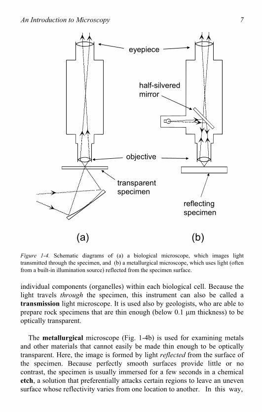
Light-optical microscopes are widely used in research and come in two basic forms. The biological microscope (Fig. 1-4a) requires an optically transparent specimen, such as a thin slice (section) of animal or plant tissue. Daylight or light from a lamp is directed via a lens or mirror through thespecimen and into the microscope, which creates a real image on the retinaof the eye or within an attached camera. Variation in the light intensity(contrast) in the image occurs because different parts of the specimenabsorb light to differing degrees. By using stains (light-absorbing chemicalsattach themselves preferentially to certain regions of the specimen), the contrast can be increased; the image of a tissue section may then reveal the
An Introduction to Microscopy 7
reflectingspecimen
transparentspecimen
objective
eyepiece
half-silveredmirror
(a) (b)
Figure 1-4. Schematic diagrams of (a) a biological microscope, which images lighttransmitted through the specimen, and (b) a metallurgical microscope, which uses light (oftenfrom a built-in illumination source) reflected from the specimen surface.
individual components (organelles) within each biological cell. Because the light travels through the specimen, this instrument can also be called atransmission light microscope. It is used also by geologists, who are able toprepare rock specimens that are thin enough (below 0.1 m thickness) to beoptically transparent.
The metallurgical microscope (Fig. 1-4b) is used for examining metals and other materials that cannot easily be made thin enough to be opticallytransparent. Here, the image is formed by light reflected from the surface ofthe specimen. Because perfectly smooth surfaces provide little or no contrast, the specimen is usually immersed for a few seconds in a chemicaletch, a solution that preferentially attacks certain regions to leave an uneven surface whose reflectivity varies from one location to another. In this way,
Chapter 18
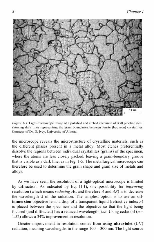
Figure 1-5. Light-microscope image of a polished and etched specimen of X70 pipeline steel,showing dark lines representing the grain boundaries between ferrite (bcc iron) crystallites.Courtesy of Dr. D. Ivey, University of Alberta.
the microscope reveals the microstructure of crystalline materials, such as the different phases present in a metal alloy. Most etches preferentiallydissolve the regions between individual crystallites (grains) of the specimen,where the atoms are less closely packed, leaving a grain-boundary groovethat is visible as a dark line, as in Fig. 1-5. The metallurgical microscope cantherefore be used to determine the grain shape and grain size of metals andalloys.
As we have seen, the resolution of a light-optical microscope is limitedby diffraction. As indicated by Eq. (1.1), one possibility for improving
resolution (which means reducing x, and therefore and R) is to decreasethe wavelength of the radiation. The simplest option is to use an oil-
immersion objective lens: a drop of a transparent liquid (refractive index n)is placed between the specimen and the objective so that the light being focused (and diffracted) has a reduced wavelength: /n. Using cedar oil (n = 1.52) allows a 34% improvement in resolution.
Greater improvement in resolution comes from using ultraviolet (UV)radiation, meaning wavelengths in the range 100 – 300 nm. The light source
An Introduction to Microscopy 9
can be a gas-discharge lamp and the final image is viewed on a phosphorscreen that converts the UV to visible light. Because ordinary glass stronglyabsorbs UV light, the focusing lenses must be made from a material such asquartz (transparent down to 190 nm) or lithium fluoride (transparent down toabout 100 nm).
1.3 The X-ray Microscope
Being electromagnetic waves with a wavelength shorter than those of UV light, x-rays offer the possibility of even better spatial resolution. This radiation cannot be focused by convex or concave lenses, as the refractiveindex of solid materials is close to that of air (1.0) at x-ray wavelengths.Instead, x-ray focusing relies on devices that make use of diffraction ratherthan refraction.
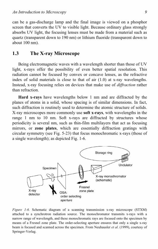
Hard x-rays have wavelengths below 1 nm and are diffracted by theplanes of atoms in a solid, whose spacing is of similar dimensions. In fact, such diffraction is routinely used to determine the atomic structure of solids. X-ray microscopes more commonly use soft x-rays, with wavelengths in therange 1 nm to 10 nm. Soft x-rays are diffracted by structures whose periodicity is several nm, such as thin-film multilayers that act as focusing mirrors, or zone plates, which are essentially diffraction gratings with circular symmetry (see Fig. 5-23) that focus monochromatic x-rays (those ofa single wavelength); as depicted Fig. 1-6.
Figure 1-6. Schematic diagram of a scanning transmission x-ray microscope (STXM)attached to a synchrotron radiation source. The monochromator transmits x-rays with anarrow range of wavelength, and these monochromatic rays are focused onto the specimen bymeans of a Fresnel zone plate. The order-selecting aperture ensures that only a single x-raybeam is focused and scanned across the specimen. From Neuhausler et al. (1999), courtesy ofSpringer-Verlag.
Chapter 110
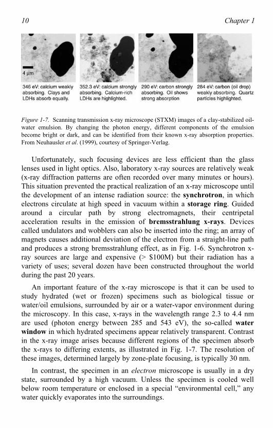
Figure 1-7. Scanning transmission x-ray microscope (STXM) images of a clay-stabilized oil-water emulsion. By changing the photon energy, different components of the emulsion become bright or dark, and can be identified from their known x-ray absorption properties. From Neuhausler et al. (1999), courtesy of Springer-Verlag.
Unfortunately, such focusing devices are less efficient than the glass lenses used in light optics. Also, laboratory x-ray sources are relatively weak (x-ray diffraction patterns are often recorded over many minutes or hours).This situation prevented the practical realization of an x-ray microscope untilthe development of an intense radiation source: the synchrotron, in whichelectrons circulate at high speed in vacuum within a storage ring. Guided around a circular path by strong electromagnets, their centripetal acceleration results in the emission of bremsstrahlung x-rays. Devices called undulators and wobblers can also be inserted into the ring; an array ofmagnets causes additional deviation of the electron from a straight-line pathand produces a strong bremsstrahlung effect, as in Fig. 1-6. Synchrotron x-ray sources are large and expensive (> $100M) but their radiation has avariety of uses; several dozen have been constructed throughout the worldduring the past 20 years.
An important feature of the x-ray microscope is that it can be used tostudy hydrated (wet or frozen) specimens such as biological tissue or water/oil emulsions, surrounded by air or a water-vapor environment duringthe microscopy. In this case, x-rays in the wavelength range 2.3 to 4.4 nmare used (photon energy between 285 and 543 eV), the so-called water
window in which hydrated specimens appear relatively transparent. Contrast in the x-ray image arises because different regions of the specimen absorb the x-rays to differing extents, as illustrated in Fig. 1-7. The resolution ofthese images, determined largely by zone-plate focusing, is typically 30 nm.
In contrast, the specimen in an electron microscope is usually in a dry state, surrounded by a high vacuum. Unless the specimen is cooled well below room temperature or enclosed in a special “environmental cell,” any water quickly evaporates into the surroundings.
An Introduction to Microscopy 11
1.4 The Transmission Electron Microscope
Early in the 20th century, physicists discovered that material particles such as electrons possess a wavelike character. Inspired by Einstein’s photon description of electromagnetic radiation, Louis de Broglie proposed that their wavelength is given by
= h /p = h/(mv) (1.5)
where h = 6.626 10-34 Js is the Planck constant; p, m, and v represent themomentum, mass, and speed of the electron. For electrons emitted into vacuum from a heated filament and accelerated through a potentialdifference of 50 V, v 4.2 106 m/s and 0.17 nm. Because this wavelength is comparable to atomic dimensions, such “slow” electrons arestrongly diffracted from the regular array of atoms at the surface of a crystal,s first observed by Davisson and Germer (1927). a
Raising the accelerating potential to 50 kV, the wavelength shrinks to about 5 pm (0.005 nm) and such higher-energy electrons can penetrate distances of several microns ( m) into a solid. If the solid is crystalline, the electrons are diffracted by atomic planes inside the material, as in the case of x-rays. It is therefore possible to form a transmission electron diffraction
pattern from electrons that have passed through a thin specimen, as first demonstrated by G.P. Thomson (1927). Later it was realized that if these transmitted electrons could be focused, their very short wavelength wouldallow the specimen to be imaged with a spatial resolution much better than the light-optical microscope.
The focusing of electrons relies on the fact that, in addition to their wavelike character, they behave as negatively charged particles and aretherefore deflected by electric or magnetic fields. This principle was used in cathode-ray tubes, TV display tubes, and computer screens. In fact, the first electron microscopes made use of technology already developed for radarapplications of cathode-ray tubes. In a transmission electron microscope
(TEM), electrons penetrate a thin specimen and are then imaged byappropriate lenses, in broad analogy with the biological light microscope(Fig. 1-4a).
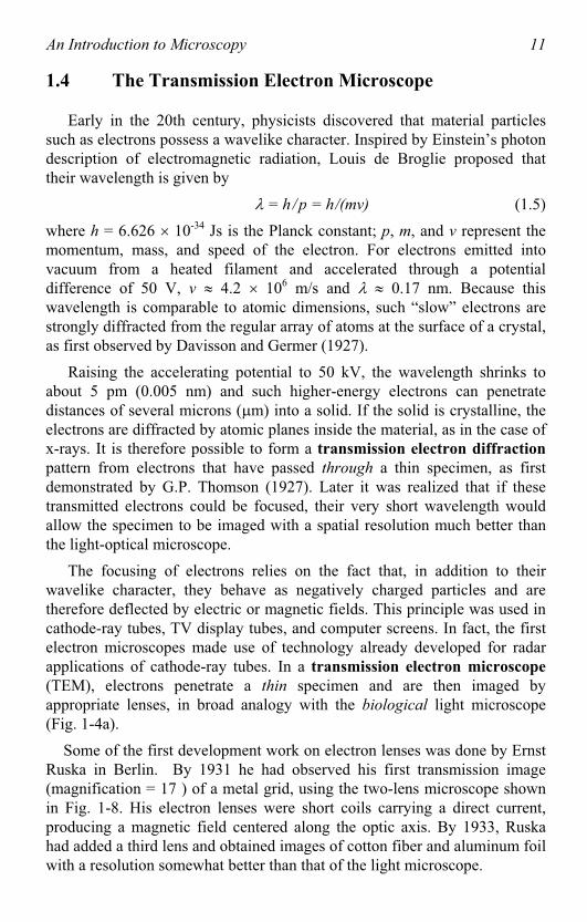
Some of the first development work on electron lenses was done by Ernst Ruska in Berlin. By 1931 he had observed his first transmission image(magnification = 17 ) of a metal grid, using the two-lens microscope shownin Fig. 1-8. His electron lenses were short coils carrying a direct current, producing a magnetic field centered along the optic axis. By 1933, Ruska had added a third lens and obtained images of cotton fiber and aluminum foil with a resolution somewhat better than that of the light microscope.
Chapter 112
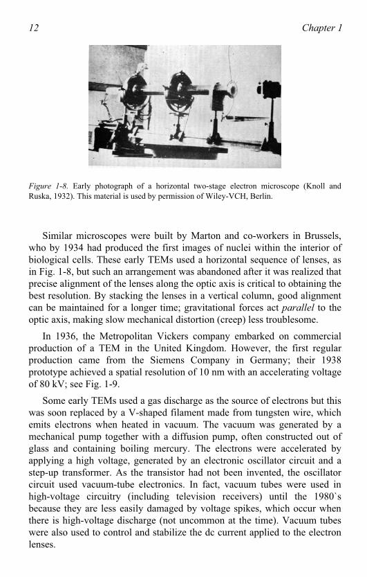
Figure 1-8. Early photograph of a horizontal two-stage electron microscope (Knoll and Ruska, 1932). This material is used by permission of Wiley-VCH, Berlin.
Similar microscopes were built by Marton and co-workers in Brussels,who by 1934 had produced the first images of nuclei within the interior ofbiological cells. These early TEMs used a horizontal sequence of lenses, asin Fig. 1-8, but such an arrangement was abandoned after it was realized that precise alignment of the lenses along the optic axis is critical to obtaining the best resolution. By stacking the lenses in a vertical column, good alignmentcan be maintained for a longer time; gravitational forces act parallel to theptic axis, making slow mechanical distortion (creep) less troublesome. o
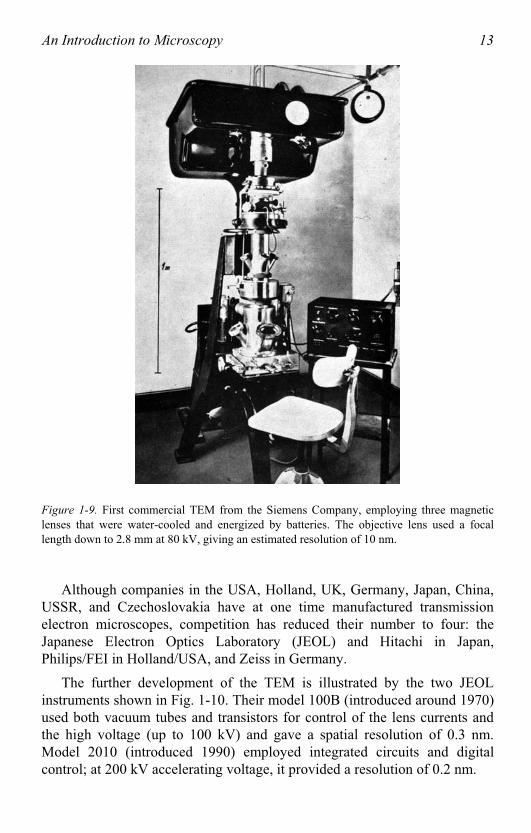
In 1936, the Metropolitan Vickers company embarked on commercial production of a TEM in the United Kingdom. However, the first regular production came from the Siemens Company in Germany; their 1938prototype achieved a spatial resolution of 10 nm with an accelerating voltage
f 80 kV; see Fig. 1-9.o
Some early TEMs used a gas discharge as the source of electrons but thiswas soon replaced by a V-shaped filament made from tungsten wire, which emits electrons when heated in vacuum. The vacuum was generated by amechanical pump together with a diffusion pump, often constructed out ofglass and containing boiling mercury. The electrons were accelerated by applying a high voltage, generated by an electronic oscillator circuit and a step-up transformer. As the transistor had not been invented, the oscillator circuit used vacuum-tube electronics. In fact, vacuum tubes were used inhigh-voltage circuitry (including television receivers) until the 1980`s because they are less easily damaged by voltage spikes, which occur whenthere is high-voltage discharge (not uncommon at the time). Vacuum tubes were also used to control and stabilize the dc current applied to the electronlenses.
An Introduction to Microscopy 13
Figure 1-9. First commercial TEM from the Siemens Company, employing three magneticlenses that were water-cooled and energized by batteries. The objective lens used a focallength down to 2.8 mm at 80 kV, giving an estimated resolution of 10 nm.
Although companies in the USA, Holland, UK, Germany, Japan, China,USSR, and Czechoslovakia have at one time manufactured transmissionelectron microscopes, competition has reduced their number to four: the Japanese Electron Optics Laboratory (JEOL) and Hitachi in Japan, Philips/FEI in Holland/USA, and Zeiss in Germany.
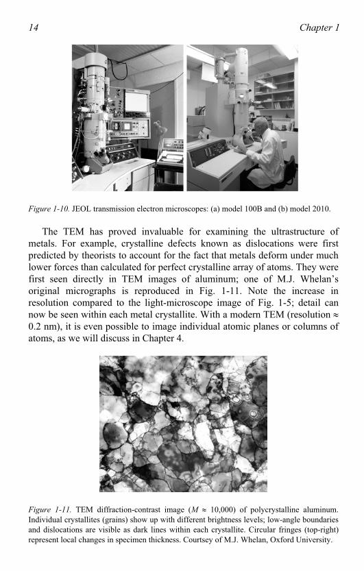
The further development of the TEM is illustrated by the two JEOLinstruments shown in Fig. 1-10. Their model 100B (introduced around 1970)used both vacuum tubes and transistors for control of the lens currents andthe high voltage (up to 100 kV) and gave a spatial resolution of 0.3 nm.Model 2010 (introduced 1990) employed integrated circuits and digitalcontrol; at 200 kV accelerating voltage, it provided a resolution of 0.2 nm.
Chapter 114
Figure 1-10. JEOL transmission electron microscopes: (a) model 100B and (b) model 2010.
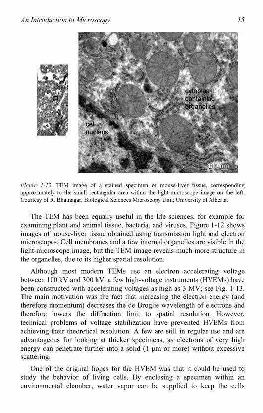
The TEM has proved invaluable for examining the ultrastructure of metals. For example, crystalline defects known as dislocations were first predicted by theorists to account for the fact that metals deform under muchlower forces than calculated for perfect crystalline array of atoms. They were first seen directly in TEM images of aluminum; one of M.J. Whelan’soriginal micrographs is reproduced in Fig. 1-11. Note the increase inresolution compared to the light-microscope image of Fig. 1-5; detail can now be seen within each metal crystallite. With a modern TEM (resolution 0.2 nm), it is even possible to image individual atomic planes or columns of atoms, as we will discuss in Chapter 4.
Figure 1-11. TEM diffraction-contrast image (M 10,000) of polycrystalline aluminum. Individual crystallites (grains) show up with different brightness levels; low-angle boundariesand dislocations are visible as dark lines within each crystallite. Circular fringes (top-right)represent local changes in specimen thickness. Courtsey of M.J. Whelan, Oxford University.
An Introduction to Microscopy 15
Figure 1-12. TEM image of a stained specimen of mouse-liver tissue, correspondingapproximately to the small rectangular area within the light-microscope image on the left.Courtesy of R. Bhatnagar, Biological Sciences Microscopy Unit, University of Alberta.
The TEM has been equally useful in the life sciences, for example for examining plant and animal tissue, bacteria, and viruses. Figure 1-12 showsimages of mouse-liver tissue obtained using transmission light and electronmicroscopes. Cell membranes and a few internal organelles are visible in the light-microscope image, but the TEM image reveals much more structure in the organelles, due to its higher spatial resolution.
Although most modern TEMs use an electron accelerating voltagebetween 100 kV and 300 kV, a few high-voltage instruments (HVEMs) have been constructed with accelerating voltages as high as 3 MV; see Fig. 1-13.The main motivation was the fact that increasing the electron energy (and therefore momentum) decreases the de Broglie wavelength of electrons and therefore lowers the diffraction limit to spatial resolution. However,technical problems of voltage stabilization have prevented HVEMs from achieving their theoretical resolution. A few are still in regular use and are advantageous for looking at thicker specimens, as electrons of very highenergy can penetrate further into a solid (1 m or more) without excessivescattering.
One of the original hopes for the HVEM was that it could be used tostudy the behavior of living cells. By enclosing a specimen within anenvironmental chamber, water vapor can be supplied to keep the cells
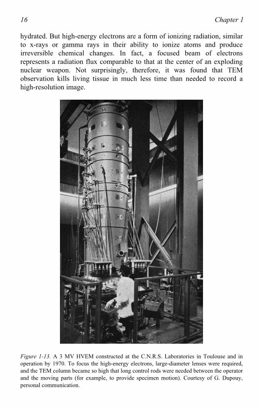
Chapter 116
hydrated. But high-energy electrons are a form of ionizing radiation, similarto x-rays or gamma rays in their ability to ionize atoms and produce irreversible chemical changes. In fact, a focused beam of electronsrepresents a radiation flux comparable to that at the center of an exploding nuclear weapon. Not surprisingly, therefore, it was found that TEMobservation kills living tissue in much less time than needed to record a high-resolution image.
Figure 1-13. A 3 MV HVEM constructed at the C.N.R.S. Laboratories in Toulouse and in operation by 1970. To focus the high-energy electrons, large-diameter lenses were required,and the TEM column became so high that long control rods were needed between the operatorand the moving parts (for example, to provide specimen motion). Courtesy of G. Dupouy,personal communication.
An Introduction to Microscopy 17
1.5 The Scanning Electron Microscope
One limitation of the TEM is that, unless the specimen is made very thin,electrons are strongly scattered within the specimen, or even absorbed ratherthan transmitted. This constraint has provided the incentive to developelectron microscopes that are capable of examining relatively thick (so-called bulk) specimens. In other words, there is need of an electron-beaminstrument that is equivalent to the metallurgical light microscope but which offers the advantage of better spatial resolution.
Electrons can indeed be “reflected” (backscattered) from a bulk specimen, as in the original experiments of Davisson and Germer (1927).But another possibility is for the incoming (primary) electrons to supplyenergy to the atomic electrons that are present in a solid, which can then bereleased as secondary electrons. These electrons are emitted with a range ofenergies, making it more difficult to focus them into an image by electron lenses. However, there is an alternative mode of image formation that uses ascanning principle: primary electrons are focused into a small-diameterelectron probe that is scanned across the specimen, making use of the factthat electrostatic or magnetic fields, applied at right angles to the beam, canbe used to change its direction of travel. By scanning simultaneously in twoperpendicular directions, a square or rectangular area of specimen (known as a raster) can be covered and an image of this area can be formed by collecting secondary electrons from each point on the specimen.
The same raster-scan signals can be used to deflect the beam generatedwithin a cathode-ray tube (CRT), in exact synchronism with the motion of the electron beam that is focused on the specimen. If the secondary-electronsignal is amplified and applied to the electron gun of the CRT (to change the number of electrons reaching the CRT screen), the resulting brightnessvariation on the phosphor represents a secondary-electron image of the specimen. In raster scanning, the image is generated serially (point by point) rather than simultaneously, as in the TEM or light microscope. A similarprinciple is used in the production and reception of television signals.
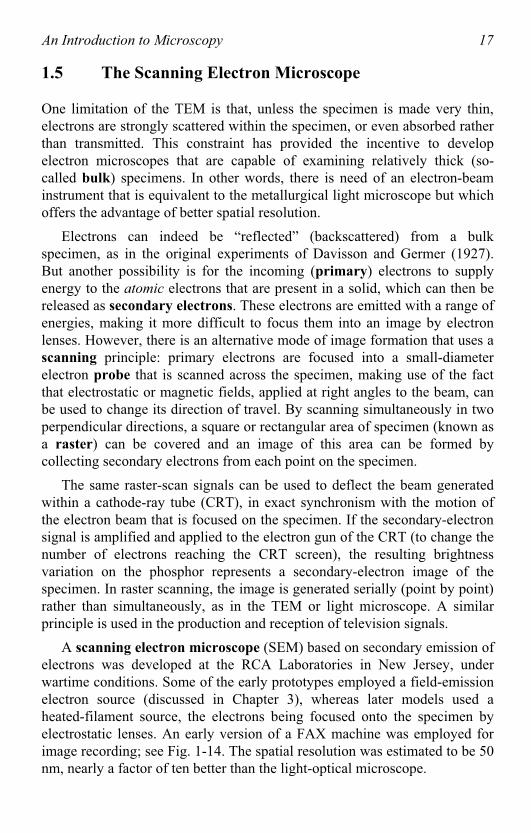
A scanning electron microscope (SEM) based on secondary emission ofelectrons was developed at the RCA Laboratories in New Jersey, underwartime conditions. Some of the early prototypes employed a field-emissionelectron source (discussed in Chapter 3), whereas later models used aheated-filament source, the electrons being focused onto the specimen by electrostatic lenses. An early version of a FAX machine was employed for image recording; see Fig. 1-14. The spatial resolution was estimated to be 50 nm, nearly a factor of ten better than the light-optical microscope.
Chapter 118
Figure 1-14. Scanning electron microscope at RCA Laboratories (Zwyorkin et al., 1942)using electrostatic lenses and vacuum-tube electronics (as in the amplifier on left of picture).An image was produced on the facsimile machine visible on the right-hand side of the picture.This material is used by permission of John Wiley & Sons, Inc.
Further SEM development occurred after the Second World War, whenCharles Oatley and colleagues began a research and construction program inthe Engineering Department at Cambridge University. Their first SEMimages were obtained in 1951, and a commercial model (built by the AEI Company) was delivered to the Pulp and Paper Research Institute of Canadain 1958.
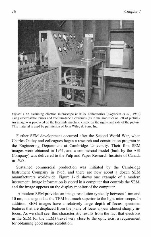
Sustained commercial production was initiated by the CambridgeInstrument Company in 1965, and there are now about a dozen SEMmanufacturers worldwide. Figure 1-15 shows one example of a moderninstrument. Image information is stored in a computer that controls the SEM, and the image appears on the display monitor of the computer.
A modern SEM provides an image resolution typically between 1 nm and10 nm, not as good as the TEM but much superior to the light microscope. Inaddition, SEM images have a relatively large depth of focus: specimenfeatures that are displaced from the plane of focus appear almost sharply in-focus. As we shall see, this characteristic results from the fact that electronsin the SEM (or the TEM) travel very close to the optic axis, a requirement for obtaining good image resolution.
An Introduction to Microscopy 19
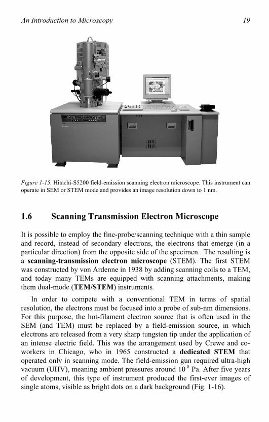
Figure 1-15. Hitachi-S5200 field-emission scanning electron microscope. This instrument canoperate in SEM or STEM mode and provides an image resolution down to 1 nm.
1.6 Scanning Transmission Electron Microscope
It is possible to employ the fine-probe/scanning technique with a thin sampleand record, instead of secondary electrons, the electrons that emerge (in a particular direction) from the opposite side of the specimen. The resulting is a scanning-transmission electron microscope (STEM). The first STEM was constructed by von Ardenne in 1938 by adding scanning coils to a TEM, and today many TEMs are equipped with scanning attachments, makingthem dual-mode (TEM/STEM) instruments.
In order to compete with a conventional TEM in terms of spatial resolution, the electrons must be focused into a probe of sub-nm dimensions. For this purpose, the hot-filament electron source that is often used in theSEM (and TEM) must be replaced by a field-emission source, in which electrons are released from a very sharp tungsten tip under the application of an intense electric field. This was the arrangement used by Crewe and co-workers in Chicago, who in 1965 constructed a dedicated STEM that operated only in scanning mode. The field-emission gun required ultra-highvacuum (UHV), meaning ambient pressures around 10-8 Pa. After five yearsof development, this type of instrument produced the first-ever images of single atoms, visible as bright dots on a dark background (Fig. 1-16).
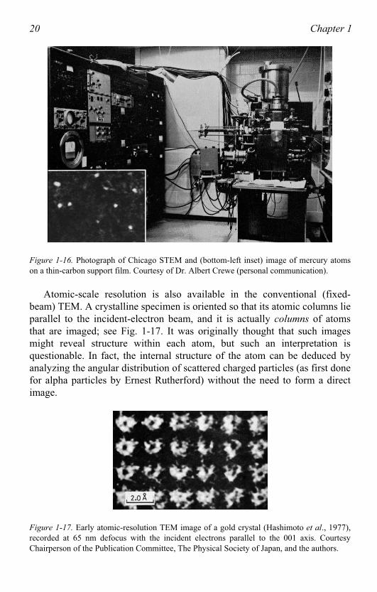
Chapter 120
Figure 1-16. Photograph of Chicago STEM and (bottom-left inset) image of mercury atomson a thin-carbon support film. Courtesy of Dr. Albert Crewe (personal communication).
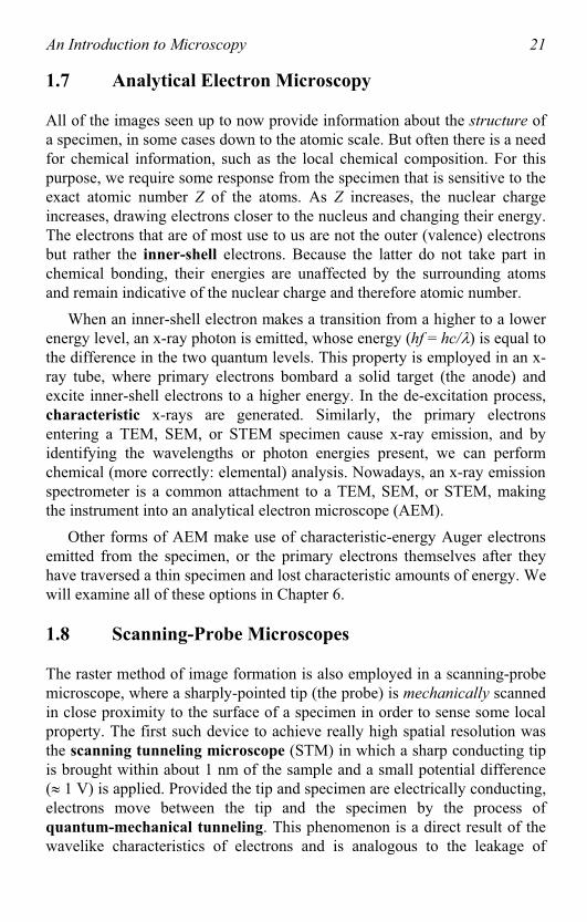
Atomic-scale resolution is also available in the conventional (fixed-beam) TEM. A crystalline specimen is oriented so that its atomic columns lieparallel to the incident-electron beam, and it is actually columns of atomsthat are imaged; see Fig. 1-17. It was originally thought that such imagesmight reveal structure within each atom, but such an interpretation is questionable. In fact, the internal structure of the atom can be deduced by analyzing the angular distribution of scattered charged particles (as first donefor alpha particles by Ernest Rutherford) without the need to form a direct image.
Figure 1-17. Early atomic-resolution TEM image of a gold crystal (Hashimoto et al., 1977),recorded at 65 nm defocus with the incident electrons parallel to the 001 axis. CourtesyChairperson of the Publication Committee, The Physical Society of Japan, and the authors.
An Introduction to Microscopy 21
1.7 Analytical Electron Microscopy
All of the images seen up to now provide information about the structure of a specimen, in some cases down to the atomic scale. But often there is a needfor chemical information, such as the local chemical composition. For thispurpose, we require some response from the specimen that is sensitive to theexact atomic number Z of the atoms. As Z increases, the nuclear chargeincreases, drawing electrons closer to the nucleus and changing their energy.The electrons that are of most use to us are not the outer (valence) electronsbut rather the inner-shell electrons. Because the latter do not take part in chemical bonding, their energies are unaffected by the surrounding atoms and remain indicative of the nuclear charge and therefore atomic number.
When an inner-shell electron makes a transition from a higher to a lower energy level, an x-ray photon is emitted, whose energy (hf = hc/ ) is equal to the difference in the two quantum levels. This property is employed in an x-ray tube, where primary electrons bombard a solid target (the anode) and excite inner-shell electrons to a higher energy. In the de-excitation process, characteristic x-rays are generated. Similarly, the primary electrons entering a TEM, SEM, or STEM specimen cause x-ray emission, and byidentifying the wavelengths or photon energies present, we can perform chemical (more correctly: elemental) analysis. Nowadays, an x-ray emissionspectrometer is a common attachment to a TEM, SEM, or STEM, making the instrument into an analytical electron microscope (AEM).
Other forms of AEM make use of characteristic-energy Auger electrons emitted from the specimen, or the primary electrons themselves after theyhave traversed a thin specimen and lost characteristic amounts of energy. Wewill examine all of these options in Chapter 6.
1.8 Scanning-Probe Microscopes
The raster method of image formation is also employed in a scanning-probemicroscope, where a sharply-pointed tip (the probe) is mechanically scanned in close proximity to the surface of a specimen in order to sense some localproperty. The first such device to achieve really high spatial resolution was the scanning tunneling microscope (STM) in which a sharp conducting tipis brought within about 1 nm of the sample and a small potential difference( 1 V) is applied. Provided the tip and specimen are electrically conducting,electrons move between the tip and the specimen by the process ofquantum-mechanical tunneling. This phenomenon is a direct result of the wavelike characteristics of electrons and is analogous to the leakage of
Chapter 122
visible-light photons between two glass surfaces brought within 1 m ofeach other (sometimes called frustrated internal reflection).
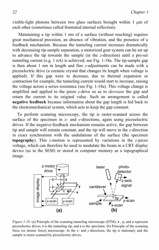
Maintaining a tip within 1 nm of a surface (without touching) requiresgreat mechanical precision, an absence of vibration, and the presence of a feedback mechanism. Because the tunneling current increases dramaticallywith decreasing tip-sample separation, a motorized gear system can be set up to advance the tip towards the sample (in the z-direction) until a pre-settunneling current (e.g. 1 nA) is achieved; see Fig. 1-18a. The tip-sample gap is then about 1 nm in length and fine z-adjustments can be made with apiezoelectric drive (a ceramic crystal that changes its length when voltage is applied). If this gap were to decrease, due to thermal expansion orcontraction for example, the tunneling current would start to increase, raisingthe voltage across a series resistance (see Fig. 1-18a). This voltage change is amplified and applied to the piezo z-drive so as to decrease the gap and return the current to its original value. Such an arrangement is callednegative feedback because information about the gap length is fed back tothe electromechanical system, which acts to keep the gap constant.
To perform scanning microscopy, the tip is raster-scanned across thesurface of the specimen in x- and y-directions, again using piezoelectricdrives. If the negative-feedback mechanism remains active, the gap betweentip and sample will remain constant, and the tip will move in the z-directionin exact synchronism with the undulations of the surface (the specimentopography). This z-motion is represented by variations in the z-piezovoltage, which can therefore be used to modulate the beam in a CRT displaydevice (as in the SEM) or stored in computer memory as a topographicalimage.
x-scan y-scan
z-motor
drive
xy
z
t s
ima
ge
dis
pla
y
tip
cantilever
x-scan
y-scan
laser photo-
detector
sample
(a) (b)
z-axis
signal
Figure 1-18. (a) Principle of the scanning tunneling microscope (STM); x , y, and z representpiezoelectric drives, t is the tunneling tip, and s is the specimen. (b) Principle of the scanningforce (or atomic force) microscope. In the x- and y-directions, the tip is stationary and thesample is raster-scanned by piezoelectric drives.
An Introduction to Microscopy 23
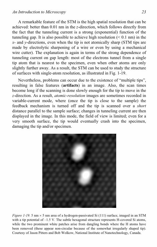
A remarkable feature of the STM is the high spatial resolution that can beachieved: better than 0.01 nm in the z-direction, which follows directly fromthe fact that the tunneling current is a strong (exponential) function of the tunneling gap. It is also possible to achieve high resolution (< 0.1 nm) in the x- and y-directions, even when the tip is not atomically sharp (STM tips are made by electrolytic sharpening of a wire or even by using a mechanicalwire cutter). The explanation is again in terms of the strong dependence of tunneling current on gap length: most of the electrons tunnel from a single tip atom that is nearest to the specimen, even when other atoms are only slightly further away. As a result, the STM can be used to study the structure of surfaces with single-atom resolution, as illustrated in Fig. 1-19.
Nevertheless, problems can occur due to the existence of “multiple tips”, resulting in false features (artifacts) in an image. Also, the scan timesbecome long if the scanning is done slowly enough for the tip to move in the z-direction. As a result, atomic-resolution images are sometimes recorded in variable-current mode, where (once the tip is close to the sample) the feedback mechanism is turned off and the tip is scanned over a short
distance parallel to the sample surface; changes in tunneling current are then displayed in the image. In this mode, the field of view is limited; even for avery smooth surface, the tip would eventually crash into the specimen,damaging the tip and/or specimen.
Figure 1-19. 5 nm 5 nm area of a hydrogen-passivated Si (111) surface, imaged in an STM with a tip potential of –1.5 V. The subtle hexagonal structure represents H-covered Si atoms, while the two prominent white patches arise from dangling bonds where the H atoms havebeen removed (these appear non-circular because of the somewhat irregularly shaped tip).Courtesy of Jason Pitters and Bob Wolkow, National Institute of Nanotechnology, Canada.
Chapter 124
Typically, the STM head is quite small, a few centimeters in dimensions;small size minimizes temperature variations (and therefore thermal drift) and forces mechanical vibrations (resonance) to higher frequencies, where theyare ore easily damped.m
The STM was developed at the IBM Zurich Laboratory (Binnig et al.,1982) and earned two of its inventors the 1986 Nobel prize in Physics(shared with Ernst Ruska, for his development of the TEM). It quicklyinspired other types of scanning-probe microscope, such as the atomic force
microscope (AFM) in which a sharp tip (at the end of a cantilever) is brought sufficiently close to the surface of a specimen, so that it essentiallytouches it and senses an interatomic force. For many years, this principle had been applied to measure the roughness of surfaces or the height of surface steps, with a height resolution of a few nanometers. But in the 1990’s, theinstrument was refined to give near-atomic resolution.
Initially, the z-motion of the cantilever was detected by locating an STMtip immediately above. Nowadays it is usually achieved by observing theangular deflection of a reflected laser beam while the specimen is scanned in the x- and y-directions; see Fig. 1-18b. AFM cantilevers can be made (fromsilicon nitride) in large quantities, using the same kind of photolithography process that yields semiconductor integrated circuits, so they are easilyreplaced when damaged or contaminated. As with the STM, scanning-forceimages must be examined critically to avoid misleading artifacts such asmu iple-tip effects.lt
The mechanical force is repulsive if the tip is in direct contact with thesample, but at a small distance above, the tip senses an attractive (van der Waals) force. Either regime may be used to provide images. Alternatively, a4-quadrant photodetector can sense torsional motion (twisting) of the AFM cantilever, which results from a sideways frictional force, giving an imagethat is essentially a map of the local coefficient of friction. Also, with amodified tip, the magnetic field of a sample can be monitored, allowing thedirect imaging of magnetic data-storage media materials for example.
Although is more difficult to obtain atomic resolution than with an STM,the AFM has the advantage that it does not require a conducting sample. Infact, the AFM can operate with its tip and specimen immersed in a liquid such as water, making the instrument valuable for imaging biologicalspecimens. This versatility, combined with its high resolution and relativelymoderate cost, has enabled the scanning probe microscope to take over someof the applications previously reserved for the SEM and TEM. However,mechanically scanning large areas of specimen is very time-consuming; it is less feasible to zoom in and out (by changing magnification) than with an
An Introduction to Microscopy 25
electron-beam instrument. Also, there is no way of implementing elementalanalysis in the AFM. An STM can be used in a spectroscopy mode but the information obtained relates to the outer-shell electron distribution and is less directly linked to chemical composition. And except in special cases, ascanning-probe image represents only the surface properties of a specimenand not the internal structure that is visible using a TEM.
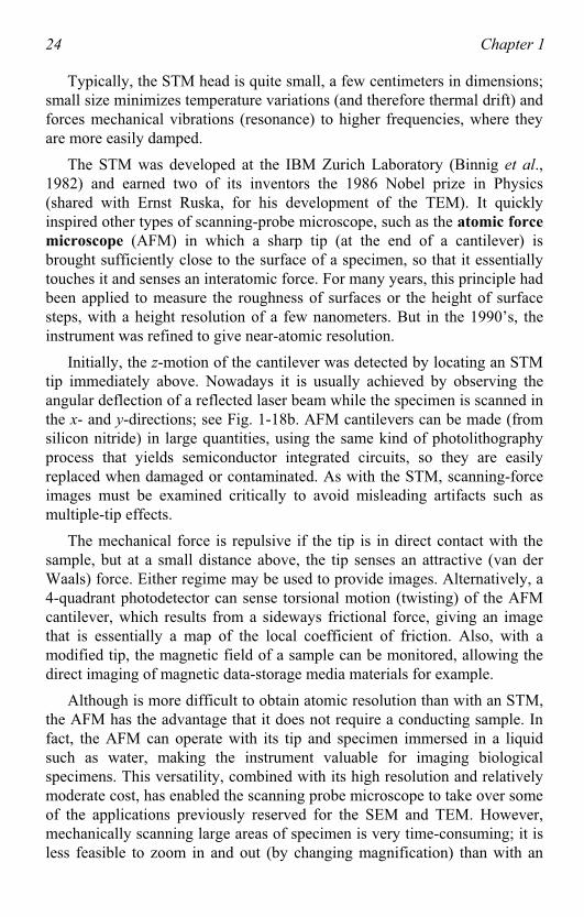
Figure 1-20a shows a typical AFM image, presented in a conventionalway in which local changes in image brightness represent variations insurface height (motion of the tip in the z-direction). However, scanning-probe images are often presented as so-called y-modulation images, in which z-motion of the tip is used to deflect the electron beam of the CRT display in the y-direction, perpendicular to its scan direction. This procedure gives athree-dimensional effect, equivalent to viewing the specimen surface at an oblique angle rather than in the perpendicular to the surface. The distance scale of this y-modulation is often magnified relative to the scale along the x-and y-scan directions, exaggerating height differences but making them moreeasily visible; see Fig. 1-20b.
Figure 1-20. AFM images of a vacuum-deposited thin film of the organic semiconductorpentacene: (a) brightness-modulation image, in which abrupt changes in image brightnessrepresent steps (terraces) on the surface, and (b) y-modulation image of the same area.Courtesy of Hui Qian, University of Alberta.
Chapter 2
ELECTRON OPTICS
Chapter 1 contained an overview of various forms of microscopy, carried out using light, electrons, and mechanical probes. In each case, the microscopeforms an enlarged image of the original object (the specimen) in order toconvey its internal or external structure. Before dealing in more detail withvarious forms of electron microscopy, we will first examine some general concepts behind image formation. These concepts were derived during the development of visible-light optics but have a range of application that ismuch wider.
2.1 Properties of an Ideal Image
Clearly, an optical image is closely related to the corresponding object, butwhat does this mean? What properties should the image have in relation tothe object? The answer to this question was provided by the Scottishphysicist James Clark Maxwell, who also developed the equations relatingelectric and magnetic fields that underlie all electrostatic and magneticphenomena, including electromagnetic waves. In a journal article (Maxwell,1858), remarkable for its clarity and for its frank comments about fellow cientists, he stated the requirements of a perfect image as follows s
1. For each point in the object, there is an equivalent point in the image.
2. The object and image are geometrically similar.
3. If the object is planar and perpendicular to the optic axis, so is the image.
Besides defining the desirable properties of an image, Maxwell’s principlesare useful for categorizing the image defects that occur (in practice) when he image is not ideal. To see this, we will discuss each rule in turn. t
28 Chapter 2
Rule 1 states that for each point in the object we can define an equivalent
point in the image. In many forms of microscopy, the connection betweenthese two points is made by some kind of particle (e.g., electron or photon)that leaves the object and ends up at the related image point. It is conveyedfrom object to image through a focusing device (such as a lens) and itstrajectory is referred to as a ray path. One particular ray path is called the optic axis; if no mirrors are involved, the optic axis is a straight line passing through the center of the lens or lenses.
How closely this rule is obeyed depends on several properties of the lens. For example, if the focusing strength is incorrect, the image formed at aparticular plane will be out-of-focus. Particles leaving a single point in the object then arrive anywhere within a circle surrounding the ideal-imagepoint, a so-called disk of confusion. But even if the focusing power isappropriate, a real lens can produce a disk of confusion because of lensaberrations: particles having different energy, or which take different paths after leaving the object, arrive displaced from the “ideal” image point. Theimage then appears blurred, with loss of fine detail, just as in the case of anout-of-focus image.
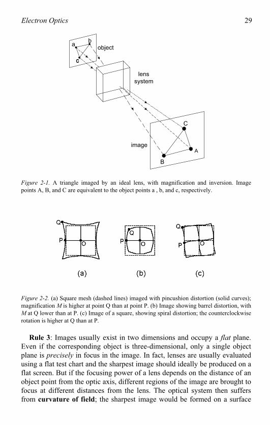
Rule 2: If we consider object points that form a pattern, their equivalent points in the image should form a similar pattern, rather than being distributed at random. For example, any three object points define a triangle and their locations in the image represent a triangle that is similar in thegeometric sense: it contains the same angles. The image triangle may have adifferent orientation than that of the object triangle; for example it could be inverted (relative to the optic axis) without violating Rule 2, as in Fig. 2-1. Also, the separations of the three image points may differ from those in theobject by a magnification factor M , in which case the image is magnified
(if M > 1) or demagnified (if M < 1).
Although the light image formed by a glass lens may appear similar to the object, close inspection often reveals the presence of distortion. This effect is most easily observed if the object contains straight lines, whichappear as curved lines in the distorted image.
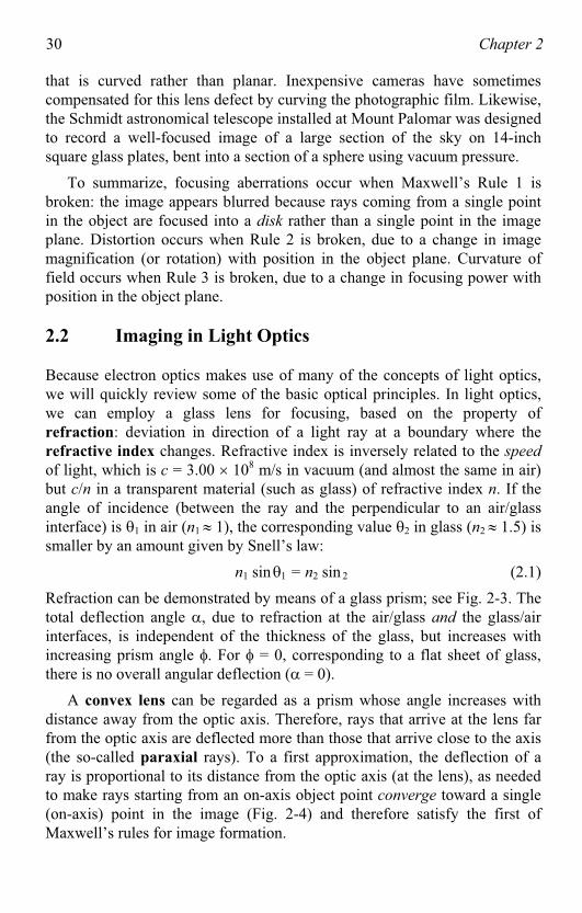
The presence of image distortion is equivalent to a variation of themagnification factor with position in the object or image: pincushion
distortion corresponds to M increasing with radial distance away from theoptic axis (Fig. 2-2a), barrel distortion corresponds to M decreasing away from the axis (Fig. 2-2b). As we will see, many electron lenses cause arotation of the image, and if this rotation increases with distance from theaxis, the result is spiral distortion (Fig. 2-2c).
Electron Optics 29
ab
c
A
B
C
lens
system
object
image
c
Figure 2-1. A triangle imaged by an ideal lens, with magnification and inversion. Imagepoints A, B, and C are equivalent to the object points a , b, and c, respectively.
Figure 2-2. (a) Square mesh (dashed lines) imaged with pincushion distortion (solid curves); magnification M is higher at point Q than at point P. (b) Image showing barrel distortion, withM at Q lower than at P. (c) Image of a square, showing spiral distortion; the counterclockwiserotation is higher at Q than at P.
Rule 3: Images usually exist in two dimensions and occupy a flat plane. Even if the corresponding object is three-dimensional, only a single object plane is precisely in focus in the image. In fact, lenses are usually evaluatedusing a flat test chart and the sharpest image should ideally be produced on a flat screen. But if the focusing power of a lens depends on the distance of anobject point from the optic axis, different regions of the image are brought tofocus at different distances from the lens. The optical system then suffersfrom curvature of field; the sharpest image would be formed on a surface
30 Chapter 2
that is curved rather than planar. Inexpensive cameras have sometimescompensated for this lens defect by curving the photographic film. Likewise, the Schmidt astronomical telescope installed at Mount Palomar was designed to record a well-focused image of a large section of the sky on 14-inchquare glass plates, bent into a section of a sphere using vacuum pressure. s
To summarize, focusing aberrations occur when Maxwell’s Rule 1 isbroken: the image appears blurred because rays coming from a single point in the object are focused into a disk rather than a single point in the imageplane. Distortion occurs when Rule 2 is broken, due to a change in imagemagnification (or rotation) with position in the object plane. Curvature of field occurs when Rule 3 is broken, due to a change in focusing power withposition in the object plane.
2.2 Imaging in Light Optics
Because electron optics makes use of many of the concepts of light optics, we will quickly review some of the basic optical principles. In light optics, we can employ a glass lens for focusing, based on the property of refraction: deviation in direction of a light ray at a boundary where the refractive index changes. Refractive index is inversely related to the speed
of light, which is c = 3.00 108 m/s in vacuum (and almost the same in air)but c/n in a transparent material (such as glass) of refractive index n. If theangle of incidence (between the ray and the perpendicular to an air/glassinterface) is 1 in air (n1 1), the corresponding value 2 in glass (n2 1.5) is smaller by an amount given by Snell’s law:
n1 sin 1 = n2 sin 2 (2.1)
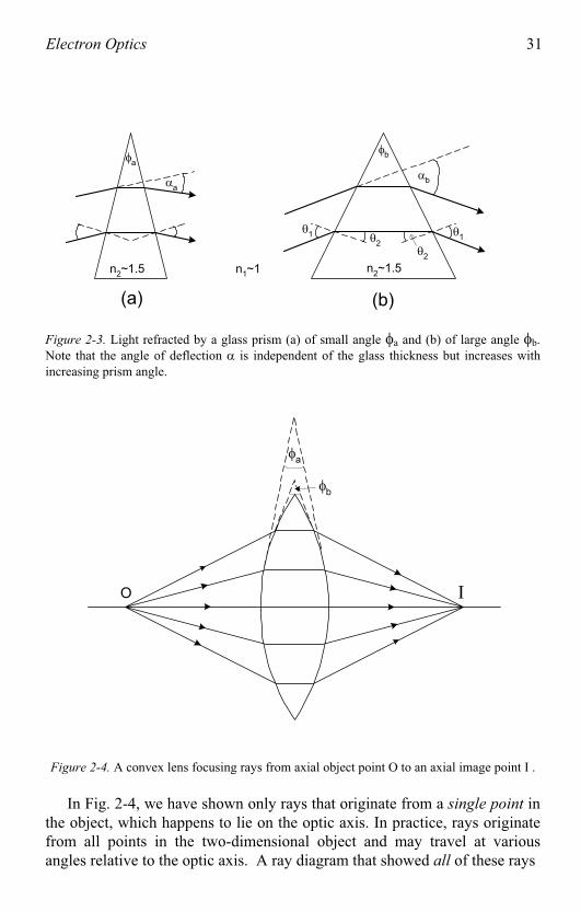
Refraction can be demonstrated by means of a glass prism; see Fig. 2-3. Thetotal deflection angle , due to refraction at the air/glass and the glass/airinterfaces, is independent of the thickness of the glass, but increases with increasing prism angle . For = 0, corresponding to a flat sheet of glass,here is no overall angular deflection ( = 0). t
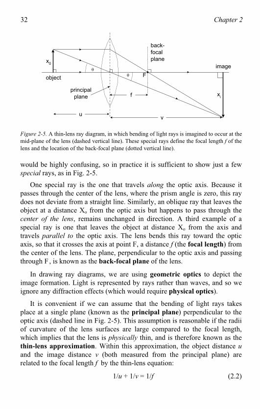
A convex lens can be regarded as a prism whose angle increases with distance away from the optic axis. Therefore, rays that arrive at the lens far from the optic axis are deflected more than those that arrive close to the axis (the so-called paraxial rays). To a first approximation, the deflection of aray is proportional to its distance from the optic axis (at the lens), as neededto make rays starting from an on-axis object point converge toward a single (on-axis) point in the image (Fig. 2-4) and therefore satisfy the first ofMaxwell’s rules for image formation.
Electron Optics 31
12
a
n1~1 n
2~1.5n
2~1.5
(a) (b)
b
1
2
ab
Figure 2-3. Light refracted by a glass prism (a) of small angle a and (b) of large angle b.Note that the angle of deflection is independent of the glass thickness but increases withincreasing prism angle.
b
a
IO
Figure 2-4. A convex lens focusing rays from axial object point O to an axial image point I .
In Fig. 2-4, we have shown only rays that originate from a single point in the object, which happens to lie on the optic axis. In practice, rays originate from all points in the two-dimensional object and may travel at various angles relative to the optic axis. A ray diagram that showed all of these rays
32 Chapter 2
uv
f
x0
xi
object
image
back-
focal
plane
F
principal
plane
Figure 2-5. A thin-lens ray diagram, in which bending of light rays is imagined to occur at themid-plane of the lens (dashed vertical line). These special rays define the focal length f of the lens and the location of the back-focal plane (dotted vertical line).
would be highly confusing, so in practice it is sufficient to show just a few special rays, as in Fig. 2-5.
One special ray is the one that travels along the optic axis. Because itpasses through the center of the lens, where the prism angle is zero, this ray does not deviate from a straight line. Similarly, an oblique ray that leaves the object at a distance Xo from the optic axis but happens to pass through thecenter of the lens, remains unchanged in direction. A third example of a special ray is one that leaves the object at distance Xo from the axis andtravels parallel to the optic axis. The lens bends this ray toward the opticaxis, so that it crosses the axis at point F, a distance f (the focal length) fromthe center of the lens. The plane, perpendicular to the optic axis and passing through F , is known as the back-focal plane of the lens.
In drawing ray diagrams, we are using geometric optics to depict theimage formation. Light is represented by rays rather than waves, and so weignore any diffraction effects (which would require physical optics).
It is convenient if we can assume that the bending of light rays takes place at a single plane (known as the principal plane) perpendicular to the optic axis (dashed line in Fig. 2-5). This assumption is reasonable if the radii of curvature of the lens surfaces are large compared to the focal length, which implies that the lens is physically thin, and is therefore known as the thin-lens approximation. Within this approximation, the object distance uand the image distance v (both measured from the principal plane) are related to the focal length f by the thin-lens equation:
1/u + 1/v = 1/f (2.2)
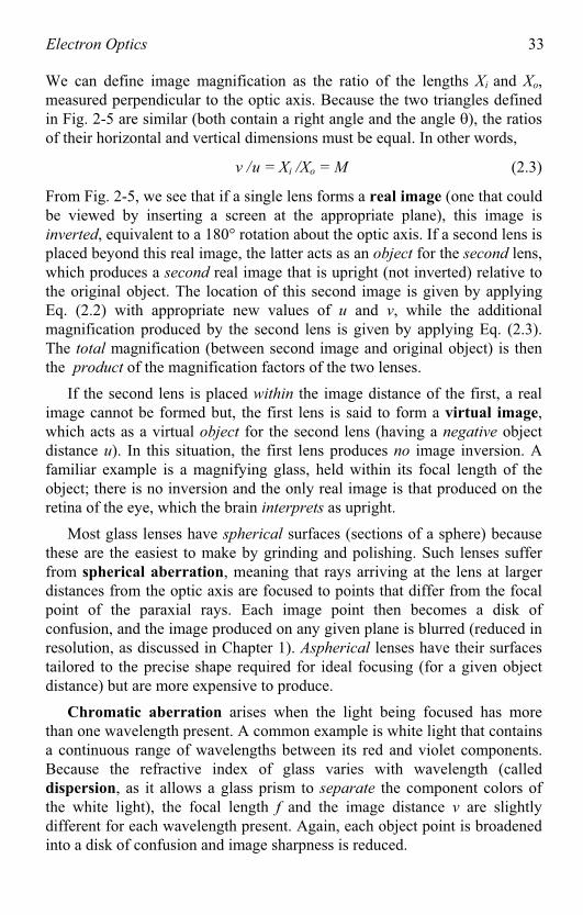
Electron Optics 33
We can define image magnification as the ratio of the lengths Xi and Xo,measured perpendicular to the optic axis. Because the two triangles defined in Fig. 2-5 are similar (both contain a right angle and the angle ), the ratios of their horizontal and vertical dimensions must be equal. In other words,
v /u = Xi /Xo = M (2.3)
From Fig. 2-5, we see that if a single lens forms a real image (one that could be viewed by inserting a screen at the appropriate plane), this image is inverted, equivalent to a 180 rotation about the optic axis. If a second lens is placed beyond this real image, the latter acts as an object for the second lens, which produces a second real image that is upright (not inverted) relative to the original object. The location of this second image is given by applyingEq. (2.2) with appropriate new values of u and v, while the additional magnification produced by the second lens is given by applying Eq. (2.3).The total magnification (between second image and original object) is then he product of the magnification factors of the two lenses.t
If the second lens is placed within the image distance of the first, a realimage cannot be formed but, the first lens is said to form a virtual image,which acts as a virtual object for the second lens (having a negative object distance u). In this situation, the first lens produces no image inversion. A familiar example is a magnifying glass, held within its focal length of theobject; there is no inversion and the only real image is that produced on the retina of the eye, which the brain interprets as upright.
Most glass lenses have spherical surfaces (sections of a sphere) becausethese are the easiest to make by grinding and polishing. Such lenses suffer from spherical aberration, meaning that rays arriving at the lens at larger distances from the optic axis are focused to points that differ from the focal point of the paraxial rays. Each image point then becomes a disk of confusion, and the image produced on any given plane is blurred (reduced in resolution, as discussed in Chapter 1). Aspherical lenses have their surfacestailored to the precise shape required for ideal focusing (for a given object distance) but are more expensive to produce.
Chromatic aberration arises when the light being focused has morethan one wavelength present. A common example is white light that contains a continuous range of wavelengths between its red and violet components.Because the refractive index of glass varies with wavelength (called dispersion, as it allows a glass prism to separate the component colors of the white light), the focal length f and the image distance v are slightlydifferent for each wavelength present. Again, each object point is broadenedinto a disk of confusion and image sharpness is reduced.
34 Chapter 2
2.3. Imaging with Electrons
Electron optics has much in common with light optics. We can imagineindividual electrons leaving an object and being focused into an image, analogous to visible-light photons. As a result of this analogy, each electron trajectory is often referred to as a ray path.
To obtain the equivalent of a convex lens for electrons, we must arrangefor the amount of deflection to increase with increasing deviation of the electron ray from the optic axis. For such focusing, we cannot rely onrefraction by a material such as glass, as electrons are strongly scattered and absorbed soon after entering a solid. Instead, we take advantage of the fact that the electron has an electrostatic charge and is therefore deflected by an electric field. Alternatively, we can use the fact that the electrons in a beamare moving; the beam is therefore equivalent to an electric current in a wire,and can be deflected by an applied magnetic field.
Electrostatic lenses
The most straightforward example of an electric field is the uniform fieldproduced between two parallel conducting plates. An electron entering sucha field would experience a constant force, regardless of its trajectory (ray path). This arrangement is suitable for deflecting an electron beam, as in acathode-ray tube, but not for focusing.
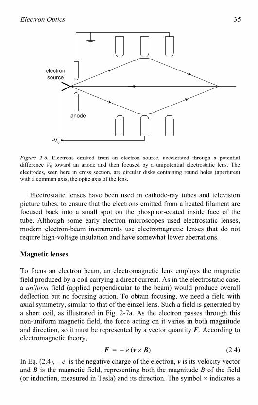
The simplest electrostatic lens consists of a circular conducting electrode(disk or tube) connected to a negative potential and containing a circular hole (aperture) centered about the optic axis. An electron passing along the optic axis is repelled equally from all points on the electrode and therefore suffers no deflection, whereas an off-axis electron is repelled by the negative charge that lies closest to it and is therefore deflected back toward the axis,as in Fig. 2-6. To a first approximation, the deflection angle is proportionalto displacement from the optic axis and a point source of electrons is focusedto a single image point.
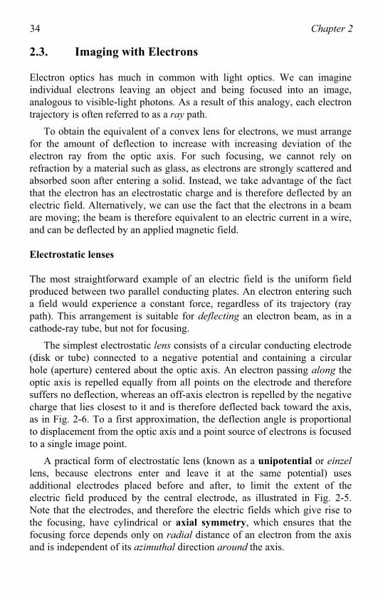
A practical form of electrostatic lens (known as a unipotential or einzel
lens, because electrons enter and leave it at the same potential) usesadditional electrodes placed before and after, to limit the extent of the electric field produced by the central electrode, as illustrated in Fig. 2-5.Note that the electrodes, and therefore the electric fields which give rise tothe focusing, have cylindrical or axial symmetry, which ensures that the focusing force depends only on radial distance of an electron from the axisand is independent of its azimuthal direction around the axis.
Electron Optics 35
-V0
electron
source
anode
Figure 2-6. Electrons emitted from an electron source, accelerated through a potentialdifference V0 toward an anode and then focused by a unipotential electrostatic lens. The electrodes, seen here in cross section, are circular disks containing round holes (apertures)with a common axis, the optic axis of the lens.
Electrostatic lenses have been used in cathode-ray tubes and televisionpicture tubes, to ensure that the electrons emitted from a heated filament are focused back into a small spot on the phosphor-coated inside face of the tube. Although some early electron microscopes used electrostatic lenses,modern electron-beam instruments use electromagnetic lenses that do notrequire high-voltage insulation and have somewhat lower aberrations.
Magnetic lenses
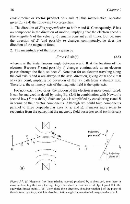
To focus an electron beam, an electromagnetic lens employs the magneticfield produced by a coil carrying a direct current. As in the electrostatic case,a uniform field (applied perpendicular to the beam) would produce overall deflection but no focusing action. To obtain focusing, we need a field with axial symmetry, similar to that of the einzel lens. Such a field is generated bya short coil, as illustrated in Fig. 2-7a. As the electron passes through this non-uniform magnetic field, the force acting on it varies in both magnitude and direction, so it must be represented by a vector quantity F . According toelectromagnetic theory,
F = e (v B) (2.4)
In Eq. (2.4), – e is the negative charge of the electron, v is its velocity vectorand B is the magnetic field, representing both the magnitude B of the field (or induction, measured in Tesla) and its direction. The symbol indicates a
36 Chapter 2
cross-product or vector product of v and B ; this mathematical operator ives Eq. (2.4) the following two properties.g
1. The direction of F is perpendicular to both v and B. Consequently, F has no component in the direction of motion, implying that the electron speed v(the magnitude of the velocity v) remains constant at all times. But becausethe direction of B (and possibly v) changes continuously, so does the
irection of the magnetic force.d
2. The magnitude F of the force is given by:
F = e v B sin( ) (2.5)
where is the instantaneous angle between v and B at the location of the electron. Because B (and possibly v) changes continuously as an electron passes through the field, so does F . Note that for an electron traveling along the coil axis, v and B are always in the axial direction, giving = 0 and F = 0 at every point, implying no deviation of the ray path from a straight line.
herefore, the symmetry axis of the magnetic field is the optic axis.T
For non-axial trajectories, the motion of the electron is more complicated.It can be analyzed in detail by using Eq. (2.4) in combination with Newton’ssecond law (F = m dv/dt). Such analysis is simplified by considering v and B
in terms of their vector components. Although we could take componentsparallel to three perpendicular axes (x, y, and z), it makes more sense torecognize from the outset that the magnetic field possesses axial (cylindrical)
O I z
vz
vrBz
Br
v z
x
trajectory
plane at O
x
(a) (b)
trajectory
plane at I
y
Figure 2-7. (a) Magnetic flux lines (dashed curves) produced by a short coil, seen here incross section, together with the trajectory of an electron from an axial object point O to theequivalent image point I. (b) View along the z-direction, showing rotation of the plane ofthe electron trajectory, which is also the rotation angle for an extended image produced at I.
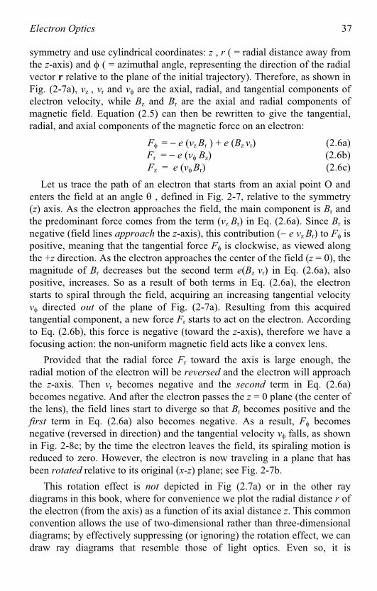
Electron Optics 37
symmetry and use cylindrical coordinates: z , r ( = radial distance away fromthe z-axis) and ( = azimuthal angle, representing the direction of the radialvector r relative to the plane of the initial trajectory). Therefore, as shown inFig. (2-7a), vz , vr and v are the axial, radial, and tangential components of electron velocity, while Bz and Br are the axial and radial components of magnetic field. Equation (2.5) can then be rewritten to give the tangential, radial, and axial components of the magnetic force on an electron:
F = e (vz Br ) + e (Bz vr) (2.6a)Fr = e (v Bz) (2.6b)Fz = e (v Br) (2.6c)
Let us trace the path of an electron that starts from an axial point O andenters the field at an angle , defined in Fig. 2-7, relative to the symmetry(z) axis. As the electron approaches the field, the main component is Br and the predominant force comes from the term (vz Br) in Eq. (2.6a). Since Br is negative (field lines approach the z-axis), this contribution ( e vz Br) to F is positive, meaning that the tangential force F is clockwise, as viewed along the +z direction. As the electron approaches the center of the field (z = 0), themagnitude of Br decreases but the second term e(Bz vr) in Eq. (2.6a), also positive, increases. So as a result of both terms in Eq. (2.6a), the electronstarts to spiral through the field, acquiring an increasing tangential velocity v directed out of the plane of Fig. (2-7a). Resulting from this acquiredtangential component, a new force Fr starts to act on the electron. According to Eq. (2.6b), this force is negative (toward the z-axis), therefore we have aocusing action: the non-uniform magnetic field acts like a convex lens.f
Provided that the radial force Fr toward the axis is large enough, theradial motion of the electron will be reversed and the electron will approach the z-axis. Then vr becomes negative and the second term in Eq. (2.6a)becomes negative. And after the electron passes the z = 0 plane (the center ofthe lens), the field lines start to diverge so that Br becomes positive and the first term in Eq. (2.6a) also becomes negative. As a result, F becomesnegative (reversed in direction) and the tangential velocity v falls, as shownin Fig. 2-8c; by the time the electron leaves the field, its spiraling motion isreduced to zero. However, the electron is now traveling in a plane that hasbeen rotated relative to its original (x-z) plane; see Fig. 2-7b.
This rotation effect is not depicted in Fig (2.7a) or in the other raydiagrams in this book, where for convenience we plot the radial distance r of the electron (from the axis) as a function of its axial distance z. This commonconvention allows the use of two-dimensional rather than three-dimensional diagrams; by effectively suppressing (or ignoring) the rotation effect, we can draw ray diagrams that resemble those of light optics. Even so, it is
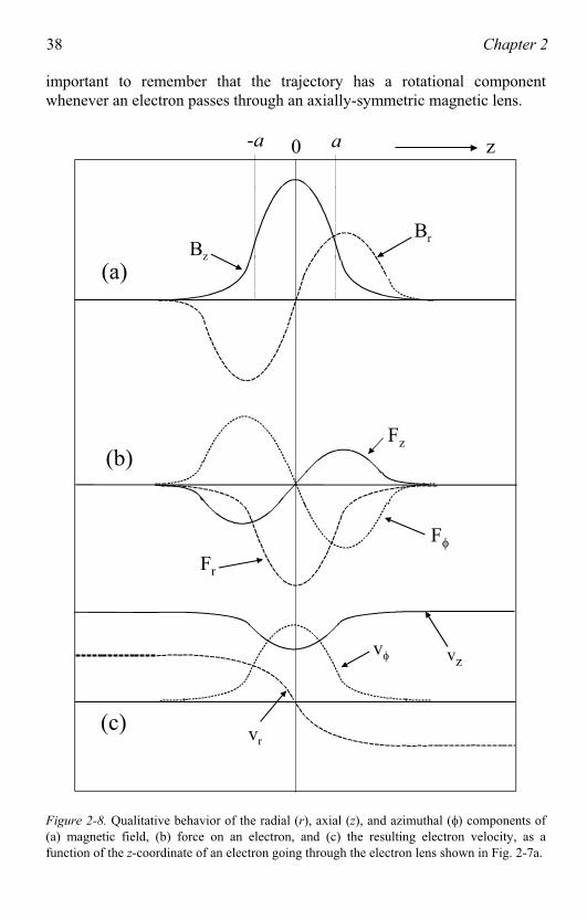
38 Chapter 2
important to remember that the trajectory has a rotational componentwhenever an electron passes through an axially-symmetric magnetic lens.
Bz
Br
Fz
Fr
F
v
vr
vz
0 z-a a
(a)
(b)
(c)
Figure 2-8. Qualitative behavior of the radial (r), axial (z), and azimuthal ( ) components of (a) magnetic field, (b) force on an electron, and (c) the resulting electron velocity, as afunction of the z-coordinate of an electron going through the electron lens shown in Fig. 2-7a.

Electron Optics 39
As we said earlier, the overall speed v of an electron in a magnetic field remains constant, so the appearance of tangential and radial components of velocity implies that vz must decrease, as depicted in Fig. 2-8c. This is in accordance with Eq. (2.6c), which predicts the existence of a third force Fz
which is negative for z < 0 (because Br < 0) and therefore acts in the –z
direction. After the electron passes the center of the lens, z , Br and Fz all become positive and vz increases back to its original value. The fact that the electron speed is constant contrasts with the case of the einzel electrostatic lens, where an electron slows down as it passes through the retarding field.
We have seen that the radial component of magnetic induction Br playsan important part in electron focusing. If a long coil (solenoid) were used togenerate the field, this component would be present only in the fringing
field at either end. (The uniform field inside the solenoid can focus electronsradiating from a point source but not a broad beam of electrons traveling parallel to its axis). So rather than using an extended magnetic field, we should make the field as short as possible. This can be done by partiallyenclosing the current-carrying coil by ferromagnetic material such as soft iron, as shown in Fig. 2-9a. Due to its high permeability, the iron carries most of the magnetic flux lines. However, the magnetic circuit contains a gap filled with nonmagnetic material, so that flux lines appear within the internal bore of the lens. The magnetic field experienced by the electronbeam can be increased and further concentrated by the use of ferromagnetic(soft iron) polepieces of small internal diameter, as illustrated in Fig. 2-9b. These polepieces are machined to high precision to ensure that the magneticfield has the high degree of axial symmetry required for good focusing.
Figure 2-9. (a) Use of ferromagnetic soft iron to concentrate magnetic field within a smallvolume. (b) Use of ferromagnetic polepieces to further concentrate the field.
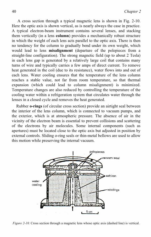
40 Chapter 2
A cross section through a typical magnetic lens is shown in Fig. 2-10.Here the optic axis is shown vertical, as is nearly always the case in practice.A typical electron-beam instrument contains several lenses, and stackingthem vertically (in a lens column) provides a mechanically robust structurein which the weight of each lens acts parallel to the optic axis. There is thenno tendency for the column to gradually bend under its own weight, which would lead to lens misalignment (departure of the polepieces from astraight-line configuration). The strong magnetic field (up to about 2 Tesla) in each lens gap is generated by a relatively large coil that contains manyturns of wire and typically carries a few amps of direct current. To removeheat generated in the coil (due to its resistance), water flows into and out of each lens. Water cooling ensures that the temperature of the lens columnreaches a stable value, not far from room temperature, so that thermalexpansion (which could lead to column misalignment) is minimized.Temperature changes are also reduced by controlling the temperature of the cooling water within a refrigeration system that circulates water through thelenses in a closed cycle and removes the heat generated.
Rubber o-rings (of circular cross section) provide an airtight seal betweenthe interior of the lens column, which is connected to vacuum pumps, and the exterior, which is at atmospheric pressure. The absence of air in the vicinity of the electron beam is essential to prevent collisions and scatteringof the electrons by air molecules. Some internal components (such as apertures) must be located close to the optic axis but adjusted in position byexternal controls. Sliding o-ring seals or thin-metal bellows are used to allowthis motion while preserving the internal vacuum.
Figure 2-10. Cross section through a magnetic lens whose optic axis (dashed line) is vertical.
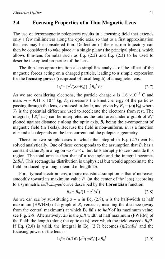
Electron Optics 41
2.4 Focusing Properties of a Thin Magnetic Lens
The use of ferromagnetic polepieces results in a focusing field that extends only a few millimeters along the optic axis, so that to a first approximationthe lens may be considered thin. Deflection of the electron trajectory can then be considered to take place at a single plane (the principal plane), which allows thin-lens formulas such as Eq. (2.2) and Eq. (2.3) to be used todescribe the optical properties of the lens.
The thin-lens approximation also simplifies analysis of the effect of the magnetic forces acting on a charged particle, leading to a simple expressionfor the focusing power (reciprocal of focal length) of a magnetic lens:
1/f = [e2/(8mE0)] Bz2 dz (2.7)
As we are considering electrons, the particle charge e is 1.6 10-19 C and mass m = 9.11 10-31 kg; E0 represents the kinetic energy of the particlespassing through the lens, expressed in Joule, and given by E0 = (e)(V0) where V0 is the potential difference used to accelerate the electrons from rest. The integral ( Bz
2 dz ) can be interpreted as the total area under a graph of Bz2
plotted against distance z along the optic axis, Bz being the z-component of magnetic field (in Tesla). Because the field is non-uniform, Bz is a function of z and also depends on the lens current and the polepiece geometry.
There are two simple cases in which the integral in Eq. (2.7) can besolved analytically. One of these corresponds to the assumption that Bz has a constant value B0 in a region –a < z < a but falls abruptly to zero outside thisregion. The total area is then that of a rectangle and the integral becomes2aB0
2. This rectangular distribution is unphysical but would approximate the field produced by a long solenoid of length 2a.
For a typical electron lens, a more realistic assumption is that B increasessmoothly toward its maximum value B0 (at the center of the lens) according to a symmetric bell-shaped curve described by the Lorentzian function:
Bz = B0 /(1 + z2/a2) (2.8)
As we can see by substituting z = a in Eq. (2.8), a is the half-width at half maximum (HWHM) of a graph of Bz versus z , meaning the distance (awayfrom the central maximum) at which Bz falls to half of its maximum value; see Fig. 2-8. Alternatively, 2a is the full width at half maximum (FWHM) of the field: the length (along the optic axis) over which the field exceeds B0/2.If Eq. (2.8) is valid, the integral in Eq. (2.7) becomes ( /2)aB0
2 and thefocusing power of the lens is
1/f = ( /16) [e2/(mE0)] aB02 (2.9)
42 Chapter 2
As an example, we can take B0 = 0.3 Tesla and a = 3 mm. If the electronsentering the lens have been accelerated from rest by applying a voltage V0 = 100 kV, we have E0 = eV0 = 1.6 × 10⁻¹⁴ J. Equation (2.9) then gives the focusing power 1/f = 93 m-1 and focal length f = 11 mm. Because f turns out to be less than twice the full-width of the field (2a = 6 mm) we mightquestion the accuracy of the thin-lens approximation in this case. In fact, more exact calculations (Reimer, 1997) show that the thin-lens formulaunderestimates f by about 14% for these parameters. For larger B0 and a,Eqs. (2.7) and (2.9) become unrealistic (see Fig. 2-13 later). In other words, strong lenses must be treated as thick lenses, for which (as in light optics) themathematical description is more complicated.
In addition, our thin-lens formula for 1/f is based on non-relativistic mechanics, in which the mass of the electron is assumed to be equal to itsrest mass. The relativistic increase in mass (predicted by Einstein’s Special Relativity) can be incorporated by replacing E0 by E0 (1 + V0 / 1022 kV) inEq. (2.9) This modification increases f by about 1% for each 10 kV of accelerating voltage, that is by 10% for V0 = 100 kV, 20% for V0 = 200 kV, and so on.
Although only approximate, Eq. (2.9) enables us to see how the focusingpower of a magnetic lens depends on the strength and spatial extent of themagnetic field and on certain properties of particles being imaged (theirkinetic energy, charge and mass). Because the kinetic energy E0 appears in the denominator of Eq. (2.7), focusing power decreases as the acceleratingvoltage is increased. As might be expected intuitively, faster electrons are deflected less in the magnetic field.
Because B0 is proportional to the current supplied to the lens windings,changing this current allows the focusing power of the lens to be varied. This ability to vary the focal length means that an electron image can be focused by adjusting the lens current. However, it also implies that the lens current must be highly stabilized (typically to within a few parts per million) toprevent unwanted changes in focusing power, which would cause the imageto drift out of focus. In light optics, change in f can only be achievedmechanically: by changing the curvature of the lens surfaces (in the case ofthe eye) or by changing the spacing between elements of a compound lens,as in the zoom lens of a camera.
When discussing qualitatively the action of a magnetic field, we saw thatthe electrons execute a spiral motion, besides being deflected back toward the optic axis. As a result, the plane containing the exit ray is rotated through an angle relative to the plane containing the incoming electron. Again making a thin-lens approximation (a << f ) and assuming a Lorentzian fielddistribution, the equations of motion can be solved to give:
Electron Optics 43
= [e/(8mE0)1/2] Bz dz = [e/(8mE0)
1/2] aB0 (2.10)
Using B0 = 0.3 T, a = 3 mm, and V0 = 100 kV as before: = 1.33 rad = 76 ,so the rotation is not unimportant. Note that this rotation is in addition to the inversion about the z-axis that occurs when a real image is formed (Fig. 2-5).In other words, the rotation of a real electron image, relative to the object, is actually radians.
Note that the image rotation would reverse (e.g., go from clockwise tocounterclockwise) if the current through the lens windings were reversed, because Bz (and therefore ) would be reversed in sign. On the other hand, reversing the current does not change the focusing power, as the integral in Eq. (2.7) involves Bz
2 , which is always positive. In fact, all of the terms in Eq. (2.7) are positive, implying that we cannot use an axially-symmetricmagnetic field to produce the electron-optical equivalent of a diverging(concave) lens, for which the focal length f would have to be negative.
Equations (2.7) (2.10) apply equally well to the focusing of other charged particles such as protons and ions, provided e and m are replaced bythe appropriate charge and mass. Equation (2.7) shows that, for the samelens current and kinetic energy (same potential used to accelerate theparticles), the focusing power of a magnetic lens is much less for theseparticles, whose mass is thousands of times larger than that of the electron. For this reason, ion optics commonly involves electrostatic lenses.
2.5 Comparison of Magnetic and Electrostatic Lenses
Some of the differences between electrostatic and magnetic lenses (of axial symmetry) are summarized in Table 2-1 and will now be discussed in turn.
Because the electrostatic force on an electron is parallel (or in the case ofan electron, antiparallel) to the field and because axially symmetric fields have no tangential component, electrostatic lenses offer the convenience of no image rotation. Their low weight and near-zero power consumption has made them attractive for space-based equipment, such as planetary probes.
The ability of electrostatic lenses to operate with voltages that slowly change (drift) or contain fluctuating components (ripple) is a result of thefact that the voltage supply that is connected to the lens can also be used to accelerate the electrons, as illustrated in Fig. 2-6. If the accelerating voltage V0 increases, the electrons travel faster; but as it requires a higher lensvoltage to focus faster electrons, the two effects cancel (to first order). Electrostatic lenses were therefore preferred in some of the early electron
44 Chapter 2
microscopes, at a time when high-voltage supplies were less stable than is possible today.
On the other hand, the fact that a voltage comparable to the acceleratingvoltage V0 must be applied to an electrostatic lens means that insulation and safety problems become severe for V0 > 50 kV. Because higher acceleratingvoltages permit better image resolution, magnetic lenses are generally preferred for electron microscopy. Magnetic lenses also provide somewhatlower aberrations, for the same focal length, further improving the imageresolution. As we will see later in this chapter, lens aberrations are also reduced by making the focal length of the objective lens small, implying amagnetic immersion lens with the specimen present within the lens field. Such a concept is problematic for an electrostatic objective, whereintroducing a conducting specimen could greatly modify the electric-fielddistribution.
Table 2-1. Comparison of electrostatic and electromagnetic lens designs.
Advantages of an electrostatic lens Advantages of a magnetic lens
No image rotation Lower lens aberrations
Lightweight, consumes no power No high-voltage insulation required
Highly stable voltage unnecessary Can be used as an immersion lens
Easier focusing of ions
2.6 Defects of Electron Lenses
For a microscope, the most important focusing defects are lens aberrations,as they reduce the spatial resolution of the image, even when it has been optimally focused. We will discuss two kinds of axial aberrations, thosethat lead to image blurring even for object points that lie on the optic axis.Similar aberrations occur in light optics.
Spherical aberration
The effect of spherical aberration can be defined by means of a diagram that shows electrons arriving at a thin lens after traveling parallel to the optic axis but not necessarily along it; see Fig. 2-11. Those that arrive very close to theoptic axis (paraxial rays, represented by dashed lines in Fig. 2-11) are brought to a focus F, a distance f from the center of the lens, at the Gaussian
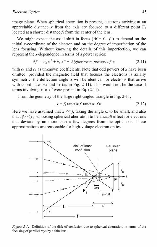
Electron Optics 45
image plane. When spherical aberration is present, electrons arriving at an appreciable distance x from the axis are focused to a different point F1
ocated at a shorter distance f1 from the center of the lens.l
We might expect the axial shift in focus ( f = f – f1 ) to depend on the initial x-coordinate of the electron and on the degree of imperfection of thelens focusing. Without knowing the details of this imperfection, we can epresent the x-dependence in terms of a power series:r
f = c2 x 2 + c4 x 4 + higher even powers of x (2.11)
with c2 and c4 as unknown coefficients. Note that odd powers of x have beenomitted: provided the magnetic field that focuses the electrons is axiallysymmetric, the deflection angle will be identical for electrons that arrive with coordinates +x and –x (as in Fig. 2-11). This would not be the case if erms involving x or x 3 were present in Eq. (2.11). t
From the geometry of the large right-angled triangle in Fig. 2-11,
x = f1 tan f tan f (2.12)
Here we have assumed that x << f, taking the angle to be small, and also that f << f , supposing spherical aberration to be a small effect for electrons that deviate by no more than a few degrees from the optic axis. These approximations are reasonable for high-voltage electron optics.
F1
rs
rs
z
+x
-x
F
Gaussian
plane
f1
f
disk of least
confusion
f
f
f/4
Figure 2-11. Definition of the disk of confusion due to spherical aberration, in terms of the focusing of parallel rays by a thin lens.
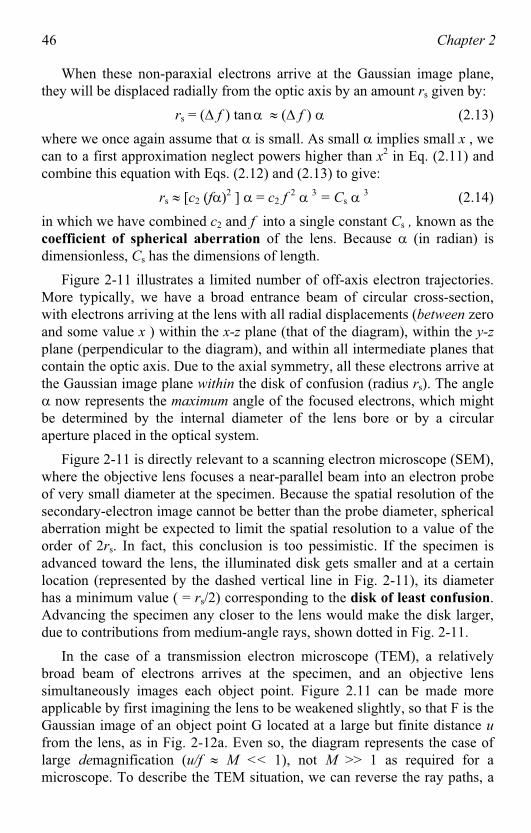
46 Chapter 2
When these non-paraxial electrons arrive at the Gaussian image plane, they will be displaced radially from the optic axis by an amount rs given by:
rs = ( f ) tan ( f ) (2.13)
where we once again assume that is small. As small implies small x , wecan to a first approximation neglect powers higher than x2 in Eq. (2.11) andombine this equation with Eqs. (2.12) and (2.13) to give:c
rs [c2 (f )2 ] = c2 f 2 3 = Cs3 (2.14)
in which we have combined c2 and f into a single constant Cs , known as the coefficient of spherical aberration of the lens. Because (in radian) is dimensionless, Cs has the dimensions of length.
Figure 2-11 illustrates a limited number of off-axis electron trajectories.More typically, we have a broad entrance beam of circular cross-section,with electrons arriving at the lens with all radial displacements (between zeroand some value x ) within the x-z plane (that of the diagram), within the y-z
plane (perpendicular to the diagram), and within all intermediate planes thatcontain the optic axis. Due to the axial symmetry, all these electrons arrive at the Gaussian image plane within the disk of confusion (radius rs). The angle
now represents the maximum angle of the focused electrons, which mightbe determined by the internal diameter of the lens bore or by a circular aperture placed in the optical system.
Figure 2-11 is directly relevant to a scanning electron microscope (SEM), where the objective lens focuses a near-parallel beam into an electron probeof very small diameter at the specimen. Because the spatial resolution of the secondary-electron image cannot be better than the probe diameter, spherical aberration might be expected to limit the spatial resolution to a value of the order of 2rs. In fact, this conclusion is too pessimistic. If the specimen isadvanced toward the lens, the illuminated disk gets smaller and at a certain location (represented by the dashed vertical line in Fig. 2-11), its diameterhas a minimum value ( = rs/2) corresponding to the disk of least confusion.Advancing the specimen any closer to the lens would make the disk larger,due to contributions from medium-angle rays, shown dotted in Fig. 2-11.
In the case of a transmission electron microscope (TEM), a relativelybroad beam of electrons arrives at the specimen, and an objective lens simultaneously images each object point. Figure 2.11 can be made moreapplicable by first imagining the lens to be weakened slightly, so that F is the Gaussian image of an object point G located at a large but finite distance ufrom the lens, as in Fig. 2-12a. Even so, the diagram represents the case oflarge demagnification (u/f M << 1), not M >> 1 as required for a microscope. To describe the TEM situation, we can reverse the ray paths, a
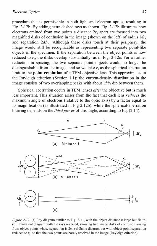
Electron Optics 47
procedure that is permissible in both light and electron optics, resulting in Fig. 2-12b. By adding extra dashed rays as shown, Fig. 2-12b illustrates how electrons emitted from two points a distance 2rs apart are focused into two magnified disks of confusion in the image (shown on the left) of radius Mrs
and separation 2Mrs. Although these disks touch at their periphery, the image would still be recognizable as representing two separate point-likeobjects in the specimen. If the separation between the object points is now reduced to rs, the disks overlap substantially, as in Fig. 2-12c. For a further reduction in spacing, the two separate point objects would no longer be distinguishable from the image, and so we take rs as the spherical-aberration limit to the point resolution of a TEM objective lens. This approximates tothe Rayleigh criterion (Section 1.1); the current-density distribution in theimage consists of two overlapping peaks with about 15% dip between them.
Spherical aberration occurs in TEM lenses after the objective but is muchless important. This situation arises from the fact that each lens reduces the maximum angle of electrons (relative to the optic axis) by a factor equal to its magnification (as illustrated in Fig 2.12b), while the spherical-aberration blurring depends on the third power of this angle, according to Eq. (2.14).
G
2rs
(a)
(b)
(c)
2rs
rs
2Mrs
Mrs
u
M ~ f/u << 1
M ~ u/f >> 1
Figure 2-12. (a) Ray diagram similar to Fig. 2-11, with the object distance u large but finite. (b) Equivalent diagram with the rays reversed, showing two image disks of confusion arising from object points whose separation is 2rs. (c) Same diagram but with object-point separationreduced to rs so that the two points are barely resolved in the image (Rayleigh criterion).
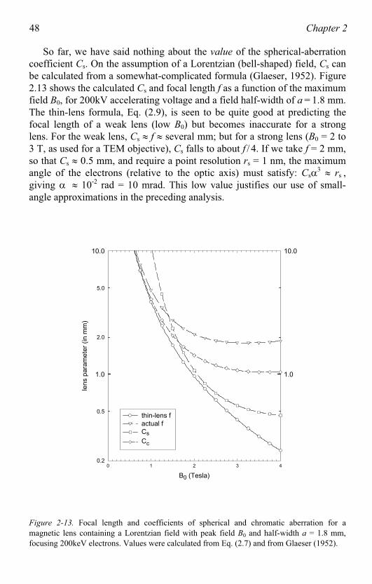
48 Chapter 2
So far, we have said nothing about the value of the spherical-aberrationcoefficient Cs. On the assumption of a Lorentzian (bell-shaped) field, Cs can be calculated from a somewhat-complicated formula (Glaeser, 1952). Figure2.13 shows the calculated Cs and focal length f as a function of the maximumfield B0, for 200kV accelerating voltage and a field half-width of a = 1.8 mm.The thin-lens formula, Eq. (2.9), is seen to be quite good at predicting thefocal length of a weak lens (low B0) but becomes inaccurate for a strong lens. For the weak lens, Cs f several mm; but for a strong lens (B0 = 2 to 3 T, as used for a TEM objective), Cs falls to about f / 4. If we take f = 2 mm,so that Cs 0.5 mm, and require a point resolution rs = 1 nm, the maximumangle of the electrons (relative to the optic axis) must satisfy: Cs
3 rs ,giving 10-2 rad = 10 mrad. This low value justifies our use of small-angle approximations in the preceding analysis.
B0 (Tesla)
0 1 2 3 4
lens
pa
ram
ete
r (i
n m
m)
0.2
0.5
2.0
5.0
1.0
10.0
1.0
10.0
thin-lens f
actual f
Cs
Cc
Figure 2-13. Focal length and coefficients of spherical and chromatic aberration for amagnetic lens containing a Lorentzian field with peak field B0 and half-width a = 1.8 mm,focusing 200keV electrons. Values were calculated from Eq. (2.7) and from Glaeser (1952).
Electron Optics 49
The basic physical properties of a magnetic field dictate that the sphericalaberration of an axially-symmetric electron lens cannot be eliminatedthrough careful design of the lens polepieces. However, spherical aberrationcan be minimized by using a strong lens (small f ). The smallest possiblefocal length is determined by the maximum field (B0 2.6 Tesla) obtainable,limited by magnetic saturation of the lens polepieces. The radius rs of thedisk of confusion is also reduced by using an aperture in the lens column to limit the maximum angular deviation of electrons from the optic axis.
Chromatic aberration
In light optics, chromatic aberration occurs when there is a spread in thewavelength of the light passing through a lens, coupled with a variation of refractive index with wavelength (dispersion). In the case of an electron, thede Broglie wavelength depends on the particle momentum, and therefore on its kinetic energy E0 , while Eq. (2.7) shows that the focusing power of amagnetic lens depends inversely on the kinetic energy. So if electrons arepresent with different kinetic energies, they will be focused at a differentdistances from a lens; for any image plane, there will be a chromatic disk of confusion rather than a point focus. The spread in kinetic energy can arisefrom several causes.
(1) Different kinetic energies of the electrons emitted from the source. For example, electrons emitted by a heated-filament source have a thermal
spread ( kT, where T is the temperature of the emitting surface) due to thestatistics of the electron-emission process.
(2) Fluctuations in the potential V0 applied to accelerate the electrons.Although high-voltage supplies are stabilized as well as possible, there isstill some drift (slow variation) and ripple (alternating component) in the accelerating voltage, and therefore in the kinetic energy eV0.
(3) Energy loss due to inelastic scattering in the specimen, a process inwhich energy is transferred from an electron to the specimen. This scatteringis also a statistical process: not all electrons lose the same amount of energy,resulting in an energy spread within the transmitted beam. Because the TEMimaging lenses focus electrons after they have passed through the specimen,inelastic scattering will cause chromatic aberration in the magnified image.
We can estimate the radius of the chromatic disk of confusion by the use of Eq. (2.7) and thin-lens geometric optics, ignoring spherical aberration and other lens defects. Consider an axial point source P of electrons (distance u
from the lens) that is focused to a point Q in the image plane (distance v
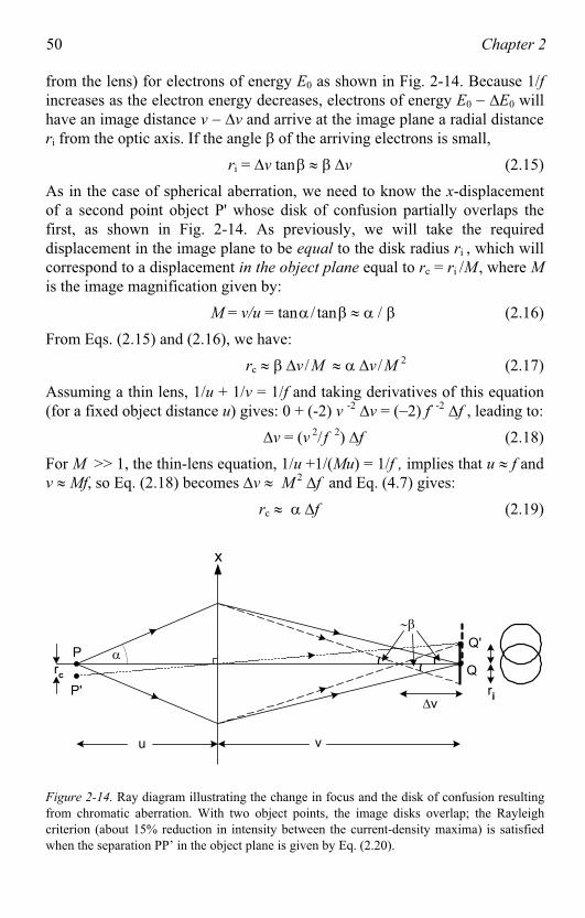
50 Chapter 2
from the lens) for electrons of energy E0 as shown in Fig. 2-14. Because 1/fincreases as the electron energy decreases, electrons of energy E0 E0 willhave an image distance v v and arrive at the image plane a radial distanceri from the optic axis. If the angle of the arriving electrons is small,
ri = v tan v (2.15)
As in the case of spherical aberration, we need to know the x-displacementof a second point object P' whose disk of confusion partially overlaps the first, as shown in Fig. 2-14. As previously, we will take the requireddisplacement in the image plane to be equal to the disk radius ri , which willcorrespond to a displacement in the object plane equal to rc = ri /M , where Ms the image magnification given by:i
M = v/u = tan / tan / (2.16)
From Eqs. (2.15) and (2.16), we have:
rc v /M v /M 2 (2.17)
Assuming a thin lens, 1/u + 1/v = 1/f and taking derivatives of this equation (for a fixed object distance u) gives: 0 + (-2) v -2 v = ( 2) f- -2 f , leading to:
v = (v 2/ f 2) f (2.18)
For M >> 1, the thin-lens equation, 1/u +1/(Mu) = 1/f , implies that u f andv , so Eq. (2.18) becomes v M 2 f and Eq. (4.7) gives:Mf
rc f (2.19)
x
P
P'
Q'
Q
u v
vri
rc
Figure 2-14. Ray diagram illustrating the change in focus and the disk of confusion resultingfrom chromatic aberration. With two object points, the image disks overlap; the Rayleighcriterion (about 15% reduction in intensity between the current-density maxima) is satisfied when the separation PP’ in the object plane is given by Eq. (2.20).
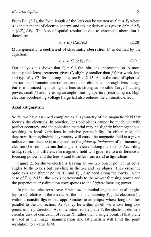
Electron Optics 51
From Eq. (2.7), the focal length of the lens can be written as f = A E0 whereA is independent of electron energy, and taking derivatives gives: f = A E0
= (f /E0) E0 . The loss of spatial resolution due to chromatic aberration is therefore:
rc f ( E0/E0) (2.20)
More generally, a coefficient of chromatic aberration Cc is defined by thequation:e
rc Cc ( E0 /E0) (2.21)
Our analysis has shown that Cc = f in the thin-lens approximation. A moreexact (thick-lens) treatment gives Cc slightly smaller than f for a weak lensand typically f/2 for a strong lens; see Fig. 2-13. As in the case of sphericalaberration, chromatic aberration cannot be eliminated through lens designbut is minimized by making the lens as strong as possible (large focusing power, small f ) and by using an angle-limiting aperture (restricting ). High electron-accelerating voltage (large E0) also reduces the chromatic effect.
Axial astigmatism
So far we have assumed complete axial symmetry of the magnetic field that focuses the electrons. In practice, lens polepieces cannot be machined withperfect accuracy, and the polepiece material may be slightly inhomogeneous, resulting in local variations in relative permeability. In either case, the departure from cylindrical symmetry will cause the magnetic field at a given radius r from the z-axis to depend on the plane of incidence of an incomingelectron (i.e., on its azimuthal angle , viewed along the z-axis). According to Eq. (2.9), this difference in magnetic field will give rise to a difference inocusing power, and the lens is said to suffer from axial astigmatism.f
Figure 2.15a shows electrons leaving an on-axis object point P at equalangles to the z-axis but traveling in the x-z and y-z planes. They cross theoptic axis at different points, Fx and Fy , displaced along the z-axis. In the case of Fig. 2-15a, the x-axis corresponds to the lowest focusing power andthe perpendicular y-direction corresponds to the highest focusing power.
In practice, electrons leave P with all azimuthal angles and at all angles (up to ) relative to the z-axis. At the plane containing Fy , the electrons liewithin a caustic figure that approximates to an ellipse whose long axis lies parallel to the x-direction. At Fx they lie within an ellipse whose long axispoints in the y-direction. At some intermediate plane F, the electrons define acircular disk of confusion of radius R , rather than a single point. If that plane is used as the image (magnification M), astigmatism will limit the point resolution to a value R/M.
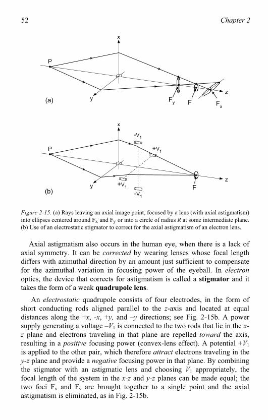
52 Chapter 2
P
zy
x
Fy F F
x
P
zy
x
F
-V1
+V1
-V1
+V1
(a)
(b)
Figure 2-15. (a) Rays leaving an axial image point, focused by a lens (with axial astigmatism)into ellipses centered around Fx and Fy or into a circle of radius R at some intermediate plane.(b) Use of an electrostatic stigmator to correct for the axial astigmatism of an electron lens.
Axial astigmatism also occurs in the human eye, when there is a lack of axial symmetry. It can be corrected by wearing lenses whose focal length differs with azimuthal direction by an amount just sufficient to compensatefor the azimuthal variation in focusing power of the eyeball. In electron
optics, the device that corrects for astigmatism is called a stigmator and ittakes the form of a weak quadrupole lens.
An electrostatic quadrupole consists of four electrodes, in the form of short conducting rods aligned parallel to the z-axis and located at equal distances along the +x, -x, +y, and –y directions; see Fig. 2-15b. A power supply generating a voltage –V1 is connected to the two rods that lie in the x-
z plane and electrons traveling in that plane are repelled toward the axis,resulting in a positive focusing power (convex-lens effect). A potential +V1
is applied to the other pair, which therefore attract electrons traveling in they-z plane and provide a negative focusing power in that plane. By combiningthe stigmator with an astigmatic lens and choosing V1 appropriately, thefocal length of the system in the x-z and y-z planes can be made equal; thetwo foci Fx and Fy are brought together to a single point and the axial astigmatism is eliminated, as in Fig. 2-15b.
Electron Optics 53
N N
S
S
zz
x
y+V
1
-V1
-V1
+V1
-V2
-V2
+V2
+V2
(a) (b)
Figure 2-16. (a) Electrostatic stigmator, viewed along the optic axis; (b) magnetic quadrupole,the basis of an electromagnetic stigmator.
In practice, we cannot predict which azimuthal direction corresponds tothe smallest or the largest focusing power of an astigmatic lens. Therefore the direction of the stigmator correction must be adjustable, as well as itsstrength. One way of achieving this is to mechanically rotate the quadrupolearound the z-axis. A more convenient arrangement is to add four moreelectrodes, connected to a second power supply that generates potentials of+V2 and –V2 , as in Fig. 2-16a. Varying the magnitude and polarity of the twovoltage supplies is equivalent to varying the strength and orientation of asingle quadrupole while avoiding the need for a rotating vacuum seal.
A more common form of stigmator consists of a magnetic quadrupole:four short solenoid coils with their axes pointing toward the optic axis. Thecoils that generate the magnetic field are connected in series and carry a common current I1. They are wired so that north and south magnetic poles face each other, as in Fig. 2-16b. Because the magnetic force on an electron is perpendicular to the magnetic field, the coils that lie along the x-axisdeflect electrons in the y-direction and vice versa. In other respects, the magnetic stigmator acts similar to the electrostatic one. Astigmatismcorrection could be achieved by adjusting the current I1 and the azimuthalorientation of the quadrupole, but in practice a second set of four coils is inserted at 45 to the first and carries a current I2 that can be varied independently. Independent adjustment of I1 and I2 enables the astigmatismto be corrected without any mechanical rotation.
54 Chapter 2
The stigmators found in electron-beam columns are weak quadrupoles,designed to correct for small deviations of in focusing power of a muchstronger lens. Strong quadrupoles are used in synchrotrons and nuclear-particle accelerators to focus high-energy electrons or other chargedparticles. Their focusing power is positive in one plane and negative(diverging, equivalent to a concave lens) in the perpendicular plane.However, a series combination of two quadrupole lenses can result in an overall convergence in both planes, without image rotation and with less power dissipation than required by an axially-symmetric lens. This last consideration is important in the case of particles heavier than the electron.
In light optics, the surfaces of a glass lens can be machined with sufficient accuracy that axial astigmatism is negligible. But for rays comingfrom an off-axis object point, the lens appears elliptical rather than round, so off-axis astigmatism is unavoidable. In electron optics, this kind ofastigmatism is not significant because the electrons are confined to smallangles relative to the optic axis (to avoid excessive spherical and chromatic aberration). Another off-axis aberration, called coma, is of some importancein a TEM if the instrument is to achieve its highest possible resolution.
Distortion and curvature of field
In an undistorted image, the distance R of an image point from the optic axis is given by R = M r , where r is the distance of the corresponding objectpoint from the axis, and the image magnification M is a constant. Distortionchanges this ideal relation to:
R = M r + Cd r 3 (2.22)
where Cd is a constant. If Cd > 0, each image point is displaced outwards, particularly those further from the optic axis, and the entire image suffersfrom pincushion distortion (Fig. 2-2c). If Cd < 0, each image point isdisplaced inward relative to the ideal image and barrel distortion is present Fig. 2-2b).(
As might be expected from the third-power dependence in Eq. (2.22),distortion is related to spherical aberration. In fact, an axially-symmetricelectron lens (for which Cs > 0) will give Cd > 0 and pincushion distortion.Barrel distortion is produced in a two-lens system in which the second lensmagnifies a virtual image produced by the first lens. In a multi-lens system,it is therefore possible to combine the two types of distortion to achieve adistortion-free image.
In the case of magnetic lenses, a third type of distortion arises from the fact that the image rotation may depend on the distance r of the object
Electron Optics 55
point from the optic axis. This spiral distortion was illustrated in Fig. 2-2c. Again, compensation is possible in a multi-lens system.
For most purposes, distortion is a less serious lens defect than aberration,because it does not result in a loss of image detail. In fact, it may not benoticeable unless the microscope specimen contains straight-line features. Insome TEMs, distortion is observed when the final (projector) lens is operated at reduced current (therefore large Cs) to achieve a low overall magnification.
Curvature of field is not a serious problem in the TEM or SEM, becausethe angular deviation of electrons from the optic axis is small. This results in a large depth of focus (the image remains acceptably sharp as the plane ofviewing is moved along the optic axis) as we will discuss in Chapter 3.
Chapter 3
THE TRANSMISSION ELECTRON
MICROSCOPE
As we saw in Chapter 1, the TEM is capable of displaying magnified imagesof a thin specimen, typically with a magnification in the range 103 to 106. Inaddition, the instrument can be used to produce electron-diffraction patterns, useful for analyzing the properties of a crystalline specimen. This overallflexibility is achieved with an electron-optical system containing an electron
gun (which produces the beam of electrons) and several magnetic lenses,stacked vertically to form a lens column. It is convenient to divide theinstrument into three sections, which we first define and then study in somedetail separately.
The illumination system comprises the electron gun, together with two or more condenser lenses that focus the electrons onto the specimen. Its design and operation determine the diameter of the electron beam (often called the “illumination”) at the specimen and the intensity level in the final TEM image.
The specimen stage allows specimens to either be held stationary or else intentionally moved, and also inserted or withdrawn from the TEM. Themechanical stability of the specimen stage is an important factor that determines the spatial resolution of the TEM image.
The imaging system contains at least three lenses that together produce a magnified image (or a diffraction pattern) of the specimen on a fluorescent screen, on photographic film, or on the monitor screen of an electroniccamera system. How this imaging system is operated determines the magnification of the TEM image, while the design of the imaging lenses largely determines the spatial resolution that can be obtained from the microscope.
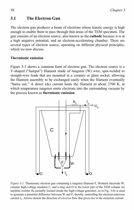
58 Chapter 3
3.1 The Electron Gun
The electron gun produces a beam of electrons whose kinetic energy is high enough to enable them to pass through thin areas of the TEM specimen. The gun consists of an electron source, also known as the cathode because it is at a high negative potential, and an electron-accelerating chamber. There areseveral types of electron source, operating on different physical principles,which we now discuss.
Thermionic emission
Figure 3-1 shows a common form of electron gun. The electron source is a V-shaped (“hairpin”) filament made of tungsten (W) wire, spot-welded tostraight-wire leads that are mounted in a ceramic or glass socket, allowingthe filament assembly to be exchanged easily when the filament eventually“burns out.” A direct (dc) current heats the filament to about 2700 K, atwhich temperature tungsten emits electrons into the surrounding vacuum bythe process known as thermionic emission.
Ie
Rb Ie-V
0
F W
C
O O
Figure 3-1. Thermionic electron gun containing a tungsten filament F, Wehnelt electrode W, ceramic high-voltage insulator C, and o-ring seal O to the lower part of the TEM column An autobias resistor Rb (actually located inside the high-voltage generator, as in Fig. 3-6) is usedto generate a potential difference between W and F, thereby controlling the electron-emissioncurrent Ie. Arrows denote the direction of electron flow that gives rise to the emission current.
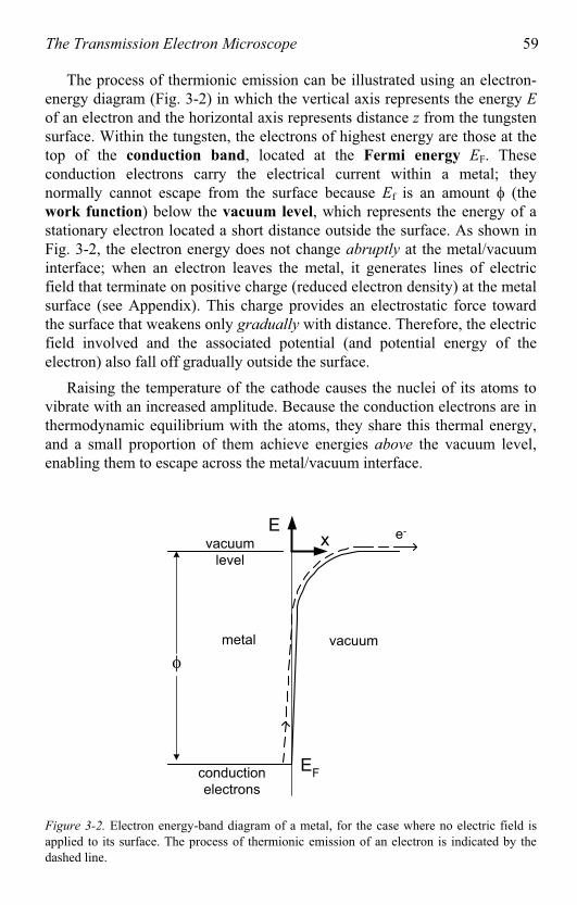
The Transmission Electron Microscope 59
The process of thermionic emission can be illustrated using an electron-energy diagram (Fig. 3-2) in which the vertical axis represents the energy E
of an electron and the horizontal axis represents distance z from the tungstensurface. Within the tungsten, the electrons of highest energy are those at thetop of the conduction band, located at the Fermi energy EF. Theseconduction electrons carry the electrical current within a metal; they normally cannot escape from the surface because Ef is an amount (thework function) below the vacuum level, which represents the energy of a stationary electron located a short distance outside the surface. As shown in Fig. 3-2, the electron energy does not change abruptly at the metal/vacuuminterface; when an electron leaves the metal, it generates lines of electricfield that terminate on positive charge (reduced electron density) at the metalsurface (see Appendix). This charge provides an electrostatic force towardthe surface that weakens only gradually with distance. Therefore, the electricfield involved and the associated potential (and potential energy of theelectron) also fall off gradually outside the surface.
Raising the temperature of the cathode causes the nuclei of its atoms tovibrate with an increased amplitude. Because the conduction electrons are inthermodynamic equilibrium with the atoms, they share this thermal energy,and a small proportion of them achieve energies above the vacuum level, enabling them to escape across the metal/vacuum interface.
EF
vacuummetal
Ex
conduction
electrons
e-
vacuum
level
Figure 3-2. Electron energy-band diagram of a metal, for the case where no electric field isapplied to its surface. The process of thermionic emission of an electron is indicated by thedashed line.
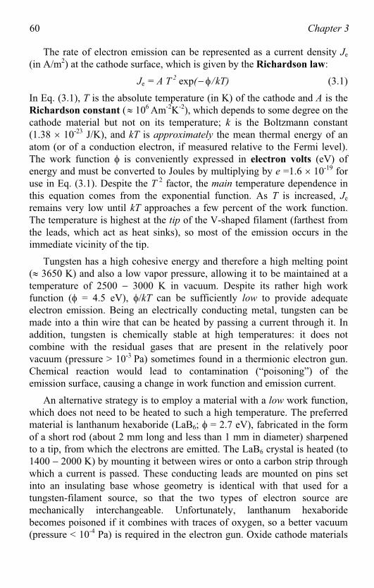
60 Chapter 3
The rate of electron emission can be represented as a current density Je
(in A/m2) at the cathode surface, which is given by the Richardson law:
Je = A T 2 exp( /kT) (3.1)
In Eq. (3.1), T is the absolute temperature (in K) of the cathode and A is the Richardson constant ( 106 Am-2K-2), which depends to some degree on thecathode material but not on its temperature; k is the Boltzmann constant(1.38 10-23 J/K), and kT is approximately the mean thermal energy of an atom (or of a conduction electron, if measured relative to the Fermi level).The work function is conveniently expressed in electron volts (eV) ofenergy and must be converted to Joules by multiplying by e =1.6 10-19 foruse in Eq. (3.1). Despite the T 2 factor, the main temperature dependence in this equation comes from the exponential function. As T is increased, Je
remains very low until kT approaches a few percent of the work function.The temperature is highest at the tip of the V-shaped filament (farthest fromthe leads, which act as heat sinks), so most of the emission occurs in the immediate vicinity of the tip.
Tungsten has a high cohesive energy and therefore a high melting point( 3650 K) and also a low vapor pressure, allowing it to be maintained at a temperature of 2500 3000 K in vacuum. Despite its rather high workfunction ( = 4.5 eV), /kT can be sufficiently low to provide adequate electron emission. Being an electrically conducting metal, tungsten can be made into a thin wire that can be heated by passing a current through it. In addition, tungsten is chemically stable at high temperatures: it does not combine with the residual gases that are present in the relatively poor vacuum (pressure > 10-3 Pa) sometimes found in a thermionic electron gun.Chemical reaction would lead to contamination (“poisoning”) of the em sion surface, causing a change in work function and emission current. is
An alternative strategy is to employ a material with a low work function,which does not need to be heated to such a high temperature. The preferredmaterial is lanthanum hexaboride (LaB6; = 2.7 eV), fabricated in the formof a short rod (about 2 mm long and less than 1 mm in diameter) sharpenedto a tip, from which the electrons are emitted. The LaB6 crystal is heated (to 1400 2000 K) by mounting it between wires or onto a carbon strip throughwhich a current is passed. These conducting leads are mounted on pins set into an insulating base whose geometry is identical with that used for a tungsten-filament source, so that the two types of electron source are mechanically interchangeable. Unfortunately, lanthanum hexaboride becomes poisoned if it combines with traces of oxygen, so a better vacuum (pressure < 10-4 Pa) is required in the electron gun. Oxide cathode materials
The Transmission Electron Microscope 61
(used in cathode-ray tubes) are even more sensitive to ambient gas and arenot used in the TEM.
Compared to a tungsten filament, the LaB6 source is relatively expensive ( $1000) but lasts longer, provided it is brought to and from its operatingtemperature slowly to avoid thermal shock and the resulting mechanicalfracture. It provides comparable emission current from a smaller cathode area, enabling the electron beam to be focused onto a smaller area of the specimen. The resulting higher current density provides a brighter image at the viewing screen (or camera) of the TEM, which is particularly importantat high image magnification.
Another important component of the electron gun (Fig. 3-1) is theWehnelt cylinder, a metal electrode that can be easily removed (to allow changing the filament or LaB6 source) but which normally surrounds the filament completely except for a small (< 1 mm diameter) hole through which the electron beam emerges. The function of the Wehnelt electrode is to control the emission current of the electron gun. For this purpose, its potential is made more negative than that of the cathode. This negative potential prevents electrons from leaving the cathode unless they are emittedfrom a region near to its tip, which is located immediately above the hole in the Wehnelt where the electrostatic potential is less negative. Increasing the magnitude of the negative bias reduces both the emitting area and the em sion current Ie .is
Although the Wehnelt bias could be provided by a voltage power supply,it is usually achieved through the autobias (or self-bias) arrangement shown in Figs. 3-1 and 3-6. A bias resistor Rb is inserted between one end of thefilament and the negative high-voltage supply ( V0) that is used to acceleratethe electrons. Because the electron current Ie emitted from the filament Fmust pass through the bias resistor, a potential difference (IeRb) is developedacross it, making the filament less negative than the Wehnelt. Changing the value of Rb provides a convenient way of intentionally varying the Wehnelt bias and therefore the emission current Ie. A further advantage of this autobias arrangement is that if the emission current Ie starts to increasespontaneously (for example, due to upward drift in the filament temperatureT ) the Wehnelt bias becomes more negative, canceling out most of theincrease in electron emission. This is another example of the negative
feedback concept discussed previously (Section 1.7).
The dependence of electron-beam current on the filament heating currentis shown in Fig. 3-3. As the current is increased from zero, the filamenttemperature eventually becomes high enough to give some emission current. At this point, the Wehnelt bias ( IeRb) is not sufficient to control the emitting
62 Chapter 3
small Rb
large Rb
saturation point
cathode temperature or filament heating current
electron
emission
current
Figure 3-3. Emission current Ie as a function of cathode temperature, for thermionic emissionfrom an autobiased (tungsten or LaB6) cathode.
area according to the feedback mechanism just described, so Ie increasesrapidly with filament temperature T, as expected from Eq. (3.1). As the filament temperature is further increased, the negative feedback mechanismstarts to operate: the beam current becomes approximately independent offilament temperature and is said to be saturated. The filament heating current (which is adjustable by the TEM operator, by turning a knob) shouldnever be set higher than the value required for current saturation. Higher values give very little increase in beam current and would result in adecrease in source lifetime, due to evaporation of W or LaB6 from the cathode. The change in Ie shown in Fig. 3-1 can be monitored from an emission-current meter or by observing the brightness of the TEM screen, allowing the filament current to be set appropriately. If the beam current needs to be changed, this is done using a bias-control knob that selects adifferent value of Rb , as indicated in Fig. 3-3.
Schottky emission
The thermionic emission of electrons can be increased by applying an electrostatic field to the cathode surface. This field lowers the height of thepotential barrier (which keeps electrons inside the cathode) by an amount(see Fig. 3-4), the so-called Schottky effect. As a result, the emission-current density Je is increased by a factor exp( /kT), typically a factor of 10as demonstrated in the Appendix.
A Schottky source consists of a pointed crystal of tungsten welded to theend of V-shaped tungsten filament. The tip is coated with zirconium oxide (ZrO) to provide a low work function ( 2.8 eV) and needs to be heated to
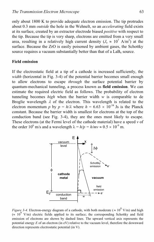
The Transmission Electron Microscope 63
only about 1800 K to provide adequate electron emission. The tip protrudesabout 0.3 mm outside the hole in the Wehnelt, so an accelerating field exists at its surface, created by an extractor electrode biased positive with respect tothe tip. Because the tip is very sharp, electrons are emitted from a very smallarea, resulting in a relatively high current density (Je 107 A/m2) at the surface. Because the ZrO is easily poisoned by ambient gases, the Schottkysource requires a vacuum substantially better than that of a LaB6 source.
Field emission
If the electrostatic field at a tip of a cathode is increased sufficiently, thewidth (horizontal in Fig. 3-4) of the potential barrier becomes small enoughto allow electrons to escape through the surface potential barrier by quantum-mechanical tunneling, a process known as field emission. We canestimate the required electric field as follows. The probability of electron tunneling becomes high when the barrier width w is comparable to de Broglie wavelength of the electron. This wavelength is related to the electron momentum p by p = h/ where h = 6.63 10-34 Js is the Planckconstant. Because the barrier width is smallest for electrons at the top of theconduction band (see Fig. 3-4), they are the ones most likely to escape.These electrons (at the Fermi level of the cathode material) have a speed v of the order 106 m/s and a wavelength = h/p = h/mv 0.5 10-9 m.
EF
vacuumcathode
metal
Ex
conduction
band
e-
vacuum
level
field
emission
Schottky
emission
e-
w
Figure 3-4. Electron-energy diagram of a cathode, with both moderate ( 108 V/m) and high
( 109 V/m) electric fields applied to its surface; the corresponding Schottky and field
emission of electrons are shown by dashed lines. The upward vertical axis represents thepotential energy E of an electron (in eV) relative to the vacuum level, therefore the downward direction represents electrostatic potential (in V).
64 Chapter 3
As seen from the right-angled triangle in Fig. 3-4, the electric field E thatgives a barrier width (at the Fermi level) of w is E = ( /e)/w. Taking w = (which allows high tunneling probability) and = 4.5 eV for a tungsten tip,so that ( /e) = 4.5 V, gives E = 4.5 / (0.5 × 10⁻⁹) 1010 V/m. In fact, such ahuge value is not necessary for field emission. Due to their high speed v,electrons arrive at the cathode surface at a very high rate, and adequate electron emission can be obtained with a tunneling probability of the orderof 10-2, which requires a surface field of the order 109 V/m.
This still-high electric field is achieved by replacing the Wehnelt cylinder(used in thermionic emission) by an extractor electrode maintained at apositive potential +V1 relative to the tip. If we approximate the tip as asphere whose radius r << distance to the extractor electrode, we can use theelectrostatic formula for an isolated sphere: E = KQ/r2 to relate the surface electric field E to the charge Q on the tip, K = 1/(4 0) being the Coulombconstant. This electric field is also the potential gradient just outside the tip: E = dV/dr, so by integration we obtain the potential of the tip (relative to its distant surroundings) as V1 = KQ/r = E r. Making the radius of curvature r of the tip very small enables the required local field E = V1/r to be producedwith practical values of V1 (a few thousand volts).
The tip is made sufficiently sharp by electrolytically dissolving the end of a short piece of tungsten wire. Electrons are emitted from an extremely smallarea ( r2 ) , resulting in an effective source diameter below 10 nm andallowing the electrons to be focused by a single demagnifying lens into an “electron probe” of sub-nanometer dimensions.
Because thermal excitation is not required, a field-emission tip can operate at room temperature, and the process is sometimes called cold field emission. As there is no evaporation of tungsten during normal operation, the tip can last for many months or even years before replacement. It is heated (“flashed”) from time to time to remove adsorbed gases, which affect the work function and cause the emission current to be unstable. Even so, cold field emission requires ultra-high vacuum (UHV: pressure 10-8 Pa) to achieve stable operation, requiring an elaborate vacuum system and resulting in substantially greater cost of the instrument.
Comparison of electron sources; source brightness
The operating conditions and the main performance criteria for the fourtypes of electron source are compared in Table 3-1. The numbers in this table are approximate but can be taken as typical for normal operation of aTEM or SEM.
The Transmission Electron Microscope 65
Table 3-1. Operating parameters of four types of electron source*
Type of source Tungstenthermionic
LaB6
thermionic
Schottkyemission
Cold field
emission
Material W LaB6 ZrO/W W
(eV) 4.5 2.7 2.8 4.5
T (K) 2700 1800 1800 300
E (V/m) low low 108 > 109
Je (A/m2) 104 106 107 109
(Am-2
/sr-1
) 109 1010 1011 1012
ds ( m) 40 10 0.02 0.01
Vacuum (Pa) < 10-2< 10-4
< 10-7 10-8
Lifetime (hours) 100 1000 104 104
E (eV) 1.5 1.0 0.5 0.3
* is the work function, T the temperature, E the electric field, Je the current density,
and the electron-optical brightness at the cathode; ds is the effective (or virtual) source
diameter, and E is the energy spread of the emitted electrons.
Although the available emission current Ie decreases as we proceed from a tungsten-filament to a field-emission source, the effective source diameterand the emitting area (As = ds
2/4) decrease by a greater factor, resulting in an increase in the current density Je. More importantly, there is an increasein a quantity known as the electron-optical brightness of the source,defined as the current density divided by the solid angle over whichelectrons are emitted:
= Ie / (As ) = Je / (3.2)
Note that in three-dimensional geometry, solid angle replaces the concept of angle in two-dimensional (Euclidean) geometry. Whereas an angle in radians is defined by = s/r, where s is arc length and r is arc radius (see Fig. 3-3a), solid angle is measured in steradians and defined as = A/r2 where A is the area of a section of a sphere at distance r (see Fig. 3-3b). Dividing by r2
akes a dimensionless number, just like .m
If electrons were emitted in every possible direction from a point source, the solid angle of emission would be = A/r2 = (4 r2)/r2 = 4 steradian. In practice, is small and is related in a simple way to the half-angle of the emission cone. Assuming small , the area of the curved end of the cone in
ig. 3-3c approximates to that of a flat disk of radius s, giving:F
( s2) /r2 = 2 (3.3)
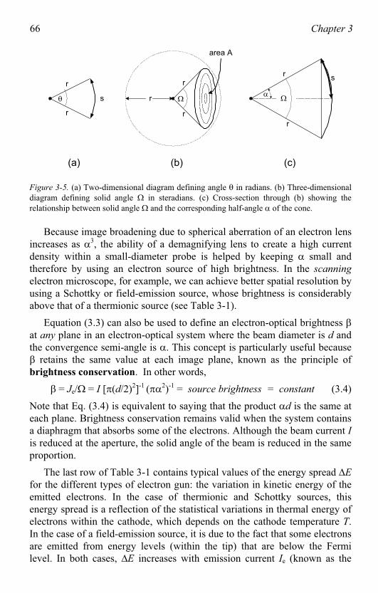
66 Chapter 3
s
rr
r
r
r
r
rs
(a) (b) (c)
area A
Figure 3-5. (a) Two-dimensional diagram defining angle in radians. (b) Three-dimensionaldiagram defining solid angle in steradians. (c) Cross-section through (b) showing therelationship between solid angle and the corresponding half-angle of the cone.
Because image broadening due to spherical aberration of an electron lensincreases as 3, the ability of a demagnifying lens to create a high currentdensity within a small-diameter probe is helped by keeping small and therefore by using an electron source of high brightness. In the scanning
electron microscope, for example, we can achieve better spatial resolution by using a Schottky or field-emission source, whose brightness is considerablyabove that of a thermionic source (see Table 3-1).
Equation (3.3) can also be used to define an electron-optical brightness at any plane in an electron-optical system where the beam diameter is d and the convergence semi-angle is . This concept is particularly useful because
retains the same value at each image plane, known as the principle of brightness conservation. In other words,
= Je/ = I [ (d/2)2]-1 ( 2)-1 = source brightness = constant (3.4)
Note that Eq. (3.4) is equivalent to saying that the product d is the same at each plane. Brightness conservation remains valid when the system containsa diaphragm that absorbs some of the electrons. Although the beam current Iis reduced at the aperture, the solid angle of the beam is reduced in the same
roportion.p
The last row of Table 3-1 contains typical values of the energy spread E
for the different types of electron gun: the variation in kinetic energy of theemitted electrons. In the case of thermionic and Schottky sources, this energy spread is a reflection of the statistical variations in thermal energy of electrons within the cathode, which depends on the cathode temperature T.In the case of a field-emission source, it is due to the fact that some electronsare emitted from energy levels (within the tip) that are below the Fermilevel. In both cases, E increases with emission current Ie (known as the
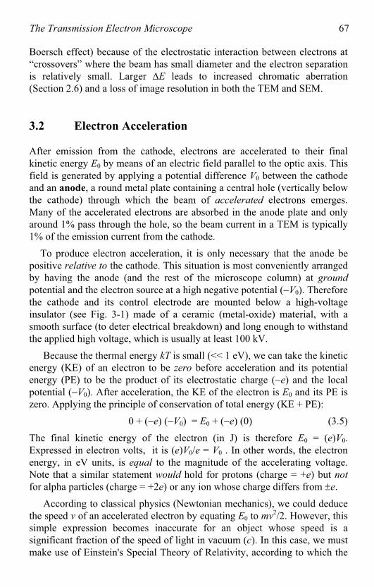
The Transmission Electron Microscope 67
Boersch effect) because of the electrostatic interaction between electrons at“crossovers” where the beam has small diameter and the electron separation is relatively small. Larger E leads to increased chromatic aberration (Section 2.6) and a loss of image resolution in both the TEM and SEM.
3.2 Electron Acceleration
After emission from the cathode, electrons are accelerated to their finalkinetic energy E0 by means of an electric field parallel to the optic axis. Thisfield is generated by applying a potential difference V0 between the cathode and an anode, a round metal plate containing a central hole (vertically belowthe cathode) through which the beam of accelerated electrons emerges.Many of the accelerated electrons are absorbed in the anode plate and onlyaround 1% pass through the hole, so the beam current in a TEM is typically
% of the emission current from the cathode. 1
To produce electron acceleration, it is only necessary that the anode be positive relative to the cathode. This situation is most conveniently arranged by having the anode (and the rest of the microscope column) at ground
potential and the electron source at a high negative potential ( V0). Thereforethe cathode and its control electrode are mounted below a high-voltageinsulator (see Fig. 3-1) made of a ceramic (metal-oxide) material, with asmooth surface (to deter electrical breakdown) and long enough to withstandhe applied high voltage, which is usually at least 100 kV.t
Because the thermal energy kT is small (<< 1 eV), we can take the kinetic energy (KE) of an electron to be zero before acceleration and its potentialenergy (PE) to be the product of its electrostatic charge ( e) and the localpotential ( V0). After acceleration, the KE of the electron is E0 and its PE is zero. Applying the principle of conservation of total energy (KE + PE):
0 + ( e) ( V0) = E0 + ( e) (0) (3.5)
The final kinetic energy of the electron (in J) is therefore E0 = (e)V0.Expressed in electron volts, it is (e)V0/e = V0 . In other words, the electronenergy, in eV units, is equal to the magnitude of the accelerating voltage. Note that a similar statement would hold for protons (charge = +e) but not
or alpha particles (charge = +2e) or any ion whose charge differs from e.f
According to classical physics (Newtonian mechanics), we could deducethe speed v of an accelerated electron by equating E0 to mv2/2. However, this simple expression becomes inaccurate for an object whose speed is a significant fraction of the speed of light in vacuum (c). In this case, we mustmake use of Einstein's Special Theory of Relativity, according to which the
68 Chapter 3
Table 3-2. Speed v and fractional increase in mass ( ) of an electron (rest mass m0) for four
values of the accelerating potential V0. The final column illustrates that the classical
expression for kinetic energy no longer applies at these high particle energies.
V0 (kV) or E0 (keV) v/c m0v2/2 (keV)
100 1.20 0.55 77
200 1.39 0.70 124
300 1.59 0.78 154
1000 2.96 0.94 226
energy of a material object can be redefined so that it includes a rest-energycomponent m0c
2, where m0 is the familiar rest mass used in classical physics.If defined in this way, the total energy E is set equal to mc2, where m = m0
is called the relativistic mass and = 1/(1 v2/c2)1/2 is a relativistic factor that represents the apparent increase in mass with speed. In other words,
E = mc2 = ( m0) c2 = E0 + m0c2 (3.6)
nd the general formula for the kinetic energy E0 is therefore: a
E0 = ( 1) m0c2 (3.7)
Applying Eq. (3.7) to an accelerated electron, we find that its speed v
reaches a significant fraction of c for the acceleration potentials V0 used in aTEM, as shown in the third column of Table 3.2. Comparison of the first andlast columns of this table indicates that, especially for the higher acceleratingvoltages, use of the classical expression m0v
2/2 would result in a substantialnderestimate of the kinetic energy of the electrons. u
The accelerating voltage ( V0) is supplied by an electronic high-voltage(HV) generator, which is connected to the electron gun by a thick, well-insulated cable. The high potential is derived from the secondary winding ofa step-up transformer, whose primary is connected to an electronic oscillatorcircuit whose (ac) output is proportional to an applied (dc) input voltage; see Fig. 3-6. Because the oscillator operates at low voltage, the large potential difference V0 appears between the primary and secondary windings of the transformer. Consequently, the secondary winding must be separated fromthe transformer core by an insulating material of sufficient thickness; it cannot be tightly wrapped around an electrically conducting soft-iron core, as in many low-voltage transformers. Because of this less-efficient magneticcoupling, the transformer operates at a frequency well above mainsfrequency (60 Hz or 50 Hz). Accordingly, the oscillator output is a high-frequency ( 10 kHz) sine wave, whose amplitude is proportional to the input voltage Vi (Fig. 3-6).
The Transmission Electron Microscope 69
To provide direct (rather than alternating) high voltage, the current from the transformer secondary is rectified by means of a series of solid-statediodes, which allow electrical current to pass only in one direction, and smoothed to remove its alternating component (ripple). Smoothing isachieved largely by the HV cable, which has enough capacitance between its inner conductor and the grounded outer sheath to short-circuit the ac-ripple omponent to ground at the operating frequency of the transformer output.c
Because the output of the oscillator circuit is linearly related to its input and rectification is also a linear process, the magnitude of the resultingaccelerating voltage is given by:
V0 = G Vi (3.8)
voltage-
controlled
oscillator
voltage-
controlled
oscillator
Rf
Rb
-V0
filament
Wehnelt
diodes
If + IeV+
Vi
If
+
-HV
tank
Figure 3-6. Schematic diagram of a TEM high-voltage generator. The meter connected to thebottom end of the secondary of the high-voltage transformer reads the sum of the emissionand feedback currents. The arrow indicates the direction of electron flow (opposite to that of the conventional current). Components within the dashed rectangle operate at high voltage.
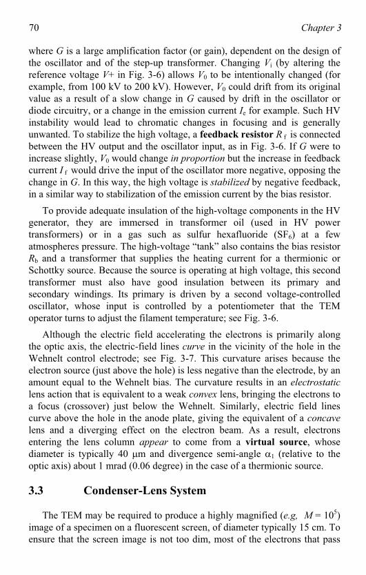
70 Chapter 3
where G is a large amplification factor (or gain), dependent on the design ofthe oscillator and of the step-up transformer. Changing Vi (by altering the reference voltage V+ in Fig. 3-6) allows V0 to be intentionally changed (forexample, from 100 kV to 200 kV). However, V0 could drift from its originalvalue as a result of a slow change in G caused by drift in the oscillator or diode circuitry, or a change in the emission current Ie for example. Such HVinstability would lead to chromatic changes in focusing and is generallyunwanted. To stabilize the high voltage, a feedback resistor R f is connectedbetween the HV output and the oscillator input, as in Fig. 3-6. If G were to increase slightly, V0 would change in proportion but the increase in feedback current I f would drive the input of the oscillator more negative, opposing thechange in G. In this way, the high voltage is stabilized by negative feedback, n a similar way to stabilization of the emission current by the bias resistor. i
To provide adequate insulation of the high-voltage components in the HV generator, they are immersed in transformer oil (used in HV powertransformers) or in a gas such as sulfur hexafluoride (SF6) at a fewatmospheres pressure. The high-voltage “tank” also contains the bias resistorRb and a transformer that supplies the heating current for a thermionic orSchottky source. Because the source is operating at high voltage, this second transformer must also have good insulation between its primary andsecondary windings. Its primary is driven by a second voltage-controlledoscillator, whose input is controlled by a potentiometer that the TEM operator turns to adjust the filament temperature; see Fig. 3-6.
Although the electric field accelerating the electrons is primarily along the optic axis, the electric-field lines curve in the vicinity of the hole in theWehnelt control electrode; see Fig. 3-7. This curvature arises because theelectron source (just above the hole) is less negative than the electrode, by anamount equal to the Wehnelt bias. The curvature results in an electrostatic
lens action that is equivalent to a weak convex lens, bringing the electrons to a focus (crossover) just below the Wehnelt. Similarly, electric field linescurve above the hole in the anode plate, giving the equivalent of a concave
lens and a diverging effect on the electron beam. As a result, electronsentering the lens column appear to come from a virtual source, whose diameter is typically 40 m and divergence semi-angle 1 (relative to theoptic axis) about 1 mrad (0.06 degree) in the case of a thermionic source.
3.3 Condenser-Lens System
The TEM may be required to produce a highly magnified (e.g, M = 105)image of a specimen on a fluorescent screen, of diameter typically 15 cm. To ensure that the screen image is not too dim, most of the electrons that pass
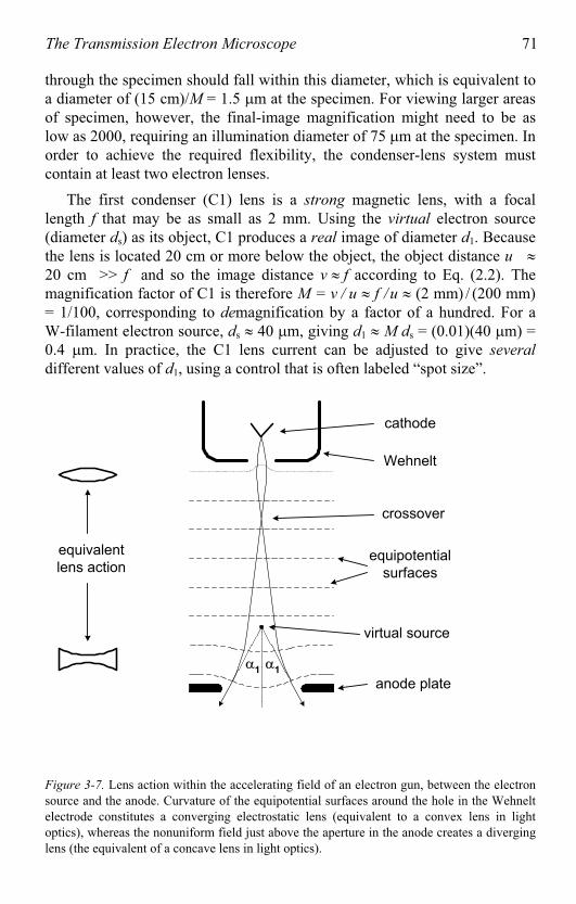
The Transmission Electron Microscope 71
through the specimen should fall within this diameter, which is equivalent to a diameter of (15 cm)/M = 1.5 m at the specimen. For viewing larger areasof specimen, however, the final-image magnification might need to be as low as 2000, requiring an illumination diameter of 75 m at the specimen. In order to achieve the required flexibility, the condenser-lens system mustcontain at least two electron lenses.
The first condenser (C1) lens is a strong magnetic lens, with a focal length f that may be as small as 2 mm. Using the virtual electron source (diameter ds) as its object, C1 produces a real image of diameter d1. Becausethe lens is located 20 cm or more below the object, the object distance u
20 cm >> f and so the image distance v f according to Eq. (2.2). Themagnification factor of C1 is therefore M = v / u f /u (2 mm) / (200 mm)= 1/100, corresponding to demagnification by a factor of a hundred. For aW-filament electron source, ds 40 m, giving d1 M ds = (0.01)(40 m) =0.4 m. In practice, the C1 lens current can be adjusted to give several
different values of d1, using a control that is often labeled “spot size”.
cathode
Wehnelt
crossover
virtual source
equipotential
surfaces
anode plate
equivalent
lens action
1 1
Figure 3-7. Lens action within the accelerating field of an electron gun, between the electronsource and the anode. Curvature of the equipotential surfaces around the hole in the Wehnelt electrode constitutes a converging electrostatic lens (equivalent to a convex lens in light optics), whereas the nonuniform field just above the aperture in the anode creates a diverginglens (the equivalent of a concave lens in light optics).
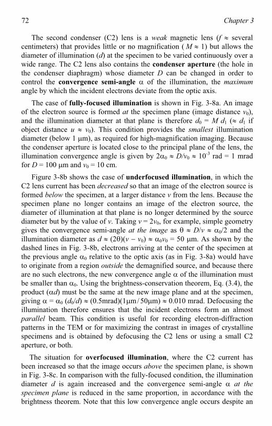
72 Chapter 3
The second condenser (C2) lens is a weak magnetic lens (f severalcentimeters) that provides little or no magnification ( M 1) but allows the diameter of illumination (d) at the specimen to be varied continuously over awide range. The C2 lens also contains the condenser aperture (the hole inthe condenser diaphragm) whose diameter D can be changed in order tocontrol the convergence semi-angle of the illumination, the maximum
angle by which the incident electrons deviate from the optic axis.
The case of fully-focused illumination is shown in Fig. 3-8a. An imageof the electron source is formed at the specimen plane (image distance v0),and the illumination diameter at that plane is therefore d0 = M d1 ( d1 ifobject distance u v0). This condition provides the smallest illuminationdiameter (below 1 m), as required for high-magnification imaging. Becausethe condenser aperture is located close to the principal plane of the lens, the illumination convergence angle is given by 2 0 D/v0 10-3 rad = 1 mradfor = 100 m and v0 = 10 cm.D
Figure 3-8b shows the case of underfocused illumination, in which the C2 lens current has been decreased so that an image of the electron source isformed below the specimen, at a larger distance v from the lens. Because thespecimen plane no longer contains an image of the electron source, the diameter of illumination at that plane is no longer determined by the source diameter but by the value of v. Taking v = 2v0, for example, simple geometry gives the convergence semi-angle at the image as D/v 0/2 and theillumination diameter as d (2 )(v v0) 0v0 = 50 m. As shown by thedashed lines in Fig. 3-8b, electrons arriving at the center of the specimen atthe previous angle 0 relative to the optic axis (as in Fig. 3-8a) would have to originate from a region outside the demagnified source, and because thereare no such electrons, the new convergence angle of the illumination mustbe smaller than 0. Using the brightness-conservation theorem, Eq. (3.4), theproduct ( d) must be the same at the new image plane and at the specimen,giving = 0 (d0/d) (0.5mrad)(1 m/ 50 m) 0.010 mrad. Defocusing theillumination therefore ensures that the incident electrons form an almostparallel beam. This condition is useful for recording electron-diffraction patterns in the TEM or for maximizing the contrast in images of crystallinespecimens and is obtained by defocusing the C2 lens or using a small C2perture, or both.a
The situation for overfocused illumination, where the C2 current hasbeen increased so that the image occurs above the specimen plane, is shown in Fig. 3-8c. In comparison with the fully-focused condition, the illuminationdiameter d is again increased and the convergence semi-angle at the
specimen plane is reduced in the same proportion, in accordance with the brightness theorem. Note that this low convergence angle occurs despite an
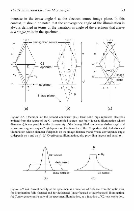
The Transmission Electron Microscope 73
increase in the beam angle at the electron-source image plane. In thiscontext, it should be noted that the convergence angle of the illumination is always defined in terms of the variation in angle of the electrons that arrive at a single point in the specimen.
(a) (b) (c)
demagnified source
C2aperture
specimen
v0
u
d1
d dd0
v'
v'
u
image
plane
image plane
u
D
d1 d1
Figure 3-8. Operation of the second condenser (C2) lens; solid rays represent electronsemitted from the center of the C1-demagnified source. (a) Fully-focused illumination whosediameter d0 is comparable to the diameter d1 of the demagnified source (see dashed rays) andwhose convergence angle (2 0) depends on the diameter of the C2 aperture. (b) Underfocusedillumination whose diameter d depends on the image distance v and whose convergence angle
depends on v and on d1. (c) Overfocused illumination, also providing large d and small .
Figure 3-9. (a) Current density at the specimen as a function of distance from the optic axis,for illumination fully focused and for defocused (underfocused or overfocused) illumination.(b) Convergence semi-angle of the specimen illumination, as a function of C2-lens excitation.
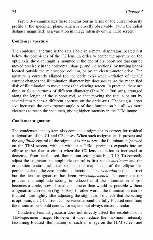
74 Chapter 3
Figure 3-9 summarizes these conclusions in terms of the current-density profile at the specimen plane, which is directly observable (with the radial distance magnified) as a variation in image intensity on the TEM screen.
Condenser aperture
The condenser aperture is the small hole in a metal diaphragm located just below the polepieces of the C2 lens. In order to center the aperture on theoptic axis, the diaphragm is mounted at the end of a support rod that can be moved precisely in the horizontal plane (x and y directions) by turning knobslocated outside the microscope column, or by an electric-motor drive. Theaperture is correctly aligned (on the optic axis) when variation of the C2 current changes the illumination diameter but does not cause the magnifieddisk of illumination to move across the viewing screen. In practice, there are three or four apertures of different diameter (D 20 200 m), arranged along the length of the support rod, so that moving the rod in or out byseveral mm places a different aperture on the optic axis. Choosing a largersize increases the convergence angle of the illumination but allows moreelectrons to reach the specimen, giving higher intensity in the TEM image.
Condenser stigmator
The condenser-lens system also contains a stigmator to correct for residual astigmatism of the C1 and C2 lenses. When such astigmatism is present and the amplitude control of the stigmator is set to zero, the illumination (viewed on the TEM screen, with or without a TEM specimen) expands into an ellipse (rather than a circle) when the C2 lens excitation is increased or decreased from the focused-illumination setting; see Fig. 3-10. To correctlyadjust the stigmator, its amplitude control is first set to maximum and the orientation control adjusted so that the major axis of the ellipse liesperpendicular to the zero-amplitude direction. The orientation is then correctbut the lens astigmatism has been overcompensated. To complete the process, the amplitude setting is reduced until the illumination ellipsebecomes a circle, now of smaller diameter than would be possible withoutastigmatism correction (Fig. 3-10e). In other words, the illumination can befocused more tightly after adjusting the stigmator. To check that the settingis optimum, the C2 current can be varied around the fully-focused condition;the illumination should contract or expand but always remain circular.
Condenser-lens astigmatism does not directly affect the resolution of aTEM-specimen image. However, it does reduce the maximum intensity(assuming focused illumination) of such an image on the TEM screen and
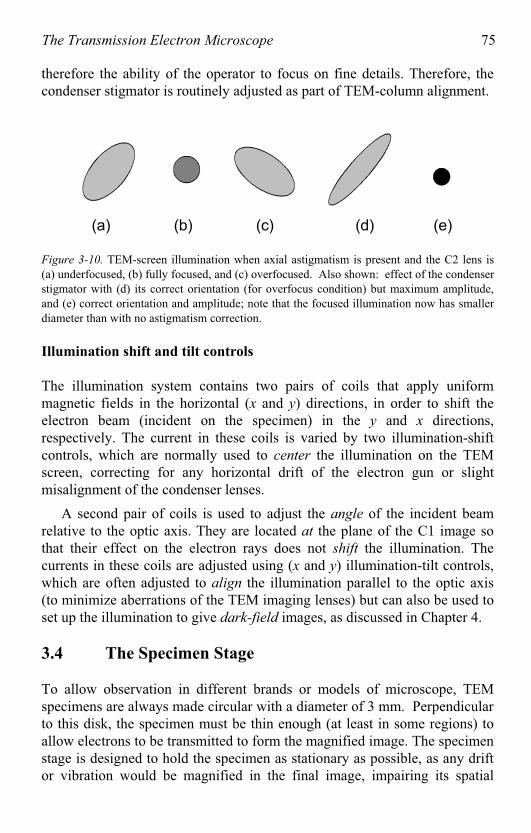
The Transmission Electron Microscope 75
therefore the ability of the operator to focus on fine details. Therefore, the condenser stigmator is routinely adjusted as part of TEM-column alignment.
(a) (b) (c) (d) (e)
Figure 3-10. TEM-screen illumination when axial astigmatism is present and the C2 lens is(a) underfocused, (b) fully focused, and (c) overfocused. Also shown: effect of the condenserstigmator with (d) its correct orientation (for overfocus condition) but maximum amplitude,and (e) correct orientation and amplitude; note that the focused illumination now has smallerdiameter than with no astigmatism correction.
Illumination shift and tilt controls
The illumination system contains two pairs of coils that apply uniformmagnetic fields in the horizontal (x and y) directions, in order to shift the electron beam (incident on the specimen) in the y and x directions,respectively. The current in these coils is varied by two illumination-shiftcontrols, which are normally used to center the illumination on the TEM screen, correcting for any horizontal drift of the electron gun or slight misalignment of the condenser lenses.
A second pair of coils is used to adjust the angle of the incident beam relative to the optic axis. They are located at the plane of the C1 image sothat their effect on the electron rays does not shift the illumination. The currents in these coils are adjusted using (x and y) illumination-tilt controls, which are often adjusted to align the illumination parallel to the optic axis (to minimize aberrations of the TEM imaging lenses) but can also be used to set up the illumination to give dark-field images, as discussed in Chapter 4.
3.4 The Specimen Stage
To allow observation in different brands or models of microscope, TEMspecimens are always made circular with a diameter of 3 mm. Perpendicularto this disk, the specimen must be thin enough (at least in some regions) to allow electrons to be transmitted to form the magnified image. The specimenstage is designed to hold the specimen as stationary as possible, as any driftor vibration would be magnified in the final image, impairing its spatial
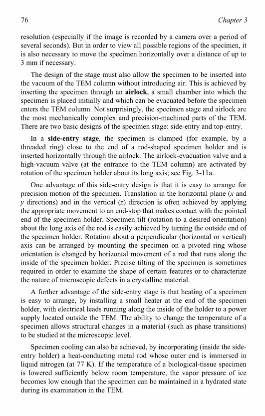
76 Chapter 3
resolution (especially if the image is recorded by a camera over a period of several seconds). But in order to view all possible regions of the specimen, it is also necessary to move the specimen horizontally over a distance of up to 3 mm if necessary.
The design of the stage must also allow the specimen to be inserted into the vacuum of the TEM column without introducing air. This is achieved byinserting the specimen through an airlock, a small chamber into which the specimen is placed initially and which can be evacuated before the specimenenters the TEM column. Not surprisingly, the specimen stage and airlock arethe most mechanically complex and precision-machined parts of the TEM. There are two basic designs of the specimen stage: side-entry and top-entry.
In a side-entry stage, the specimen is clamped (for example, by a threaded ring) close to the end of a rod-shaped specimen holder and isinserted horizontally through the airlock. The airlock-evacuation valve and ahigh-vacuum valve (at the entrance to the TEM column) are activated byrotation of the specimen holder about its long axis; see Fig. 3-11a.
One advantage of this side-entry design is that it is easy to arrange for precision motion of the specimen. Translation in the horizontal plane (x and y directions) and in the vertical (z) direction is often achieved by applyingthe appropriate movement to an end-stop that makes contact with the pointed end of the specimen holder. Specimen tilt (rotation to a desired orientation)about the long axis of the rod is easily achieved by turning the outside end of the specimen holder. Rotation about a perpendicular (horizontal or vertical) axis can be arranged by mounting the specimen on a pivoted ring whoseorientation is changed by horizontal movement of a rod that runs along theinside of the specimen holder. Precise tilting of the specimen is sometimesrequired in order to examine the shape of certain features or to characterizethe nature of microscopic defects in a crystalline material.
A further advantage of the side-entry stage is that heating of a specimenis easy to arrange, by installing a small heater at the end of the specimenholder, with electrical leads running along the inside of the holder to a power supply located outside the TEM. The ability to change the temperature of a specimen allows structural changes in a material (such as phase transitions) to be studied at the microscopic level.
Specimen cooling can also be achieved, by incorporating (inside the side-entry holder) a heat-conducting metal rod whose outer end is immersed inliquid nitrogen (at 77 K). If the temperature of a biological-tissue specimenis lowered sufficiently below room temperature, the vapor pressure of ice becomes low enough that the specimen can be maintained in a hydrated state during its examination in the TEM.
The Transmission Electron Microscope 77
One disadvantage of the side-entry design is that mechanical vibration, picked up from the TEM column or from acoustical vibrations in the external air, is transmitted directly to the specimen. In addition, any thermalexpansion of the specimen holder can cause drift of the specimen and of theTEM image. These problems have been largely overcome by careful design, including choice of materials used to construct the specimen holder. As aresult, side-entry holders are widely used, even for high-resolution imaging.
In a top-entry stage, the specimen is clamped to the bottom end of a cylindrical holder that is equipped with a conical collar; see Fig. 3-11b. Theholder is loaded into position through an airlock by means of a sliding andtilting arm, which is then detached and retracted. Inside the TEM, the cone of the specimen holder fits snugly into a conical well of the specimen stage, which can be translated in the (x and y) horizontal directions by a precisiongear mechanism.
(a) Side-entry stage
end-stop
specimen
specimen holder
high-vacuum
valve
airlock
specimen specimen holder
movablestage
top of objective lens
specimen loading rod
(b) Top-entry stage
airlock
Figure 3-11. Schematic diagrams of (a) a side-entry and (b) a top-entry specimen holder.
78 Chapter 3
The major advantage of a top-entry design is that the loading arm is disengaged after the specimen is loaded, so the specimen holder is less liableto pick up vibrations from the TEM environment. In addition, its axiallysymmetric design tends to ensure that any thermal expansion occurs radially about the optic axis and therefore becomes small close to the axis. However,it is more difficult to provide tilting, heating, or cooling of the specimen.Although such facilities have all been implemented in top-entry stages, theyrequire elaborate precision engineering, making the holder fragile and expensive. Because the specimen is held at the bottom of its holder, it is difficult to collect more than a small fraction of the x-rays that are generated by the transmitted beam and emitted in the upward direction, making this design less attractive for high-sensitivity elemental analysis (see Chapter 6).
3.5 TEM Imaging System
The imaging lenses of a TEM produce a magnified image or an electron-diffraction pattern of the specimen on a viewing screen or camera system.The spatial resolution of the image is largely dependent on the quality and design of these lenses, especially on the first imaging lens: the objective.
Objective lens
As in the case of a light-optical microscope, the lens closest to the specimenis called the objective. It is a strong lens, with a small focal length; becauseof its high excitation current, the objective must be cooled with temperature-controlled water, thereby minimizing image drift that could result fromthermal expansion of the specimen stage. Because focusing power dependson lens excitation, the current for the objective lens must be highlystabilized, using negative feedback within its dc power supply. The power supply must be able to deliver substantially different lens currents, in order to retain the same focal length for different electron-accelerating voltages. The TEM also has fine controls that enable the operator to make smallfractional adjustments to the objective current, to allow the specimen imageto be accurately focused on the viewing screen.
The objective produces a magnified real image of the specimen (M 50 to 100) at a distance v 10 cm below the center of the lens. Because of the small value of f , Eq. (2.2) indicates that the object distance u is only slightlygreater than the focal length, so the specimen is usually located within the pre-field of the lens (that part of the focusing field that acts on the electronbefore it reaches the center of the lens). By analogy with a light microscope,the objective is therefore referred to as an immersion lens.
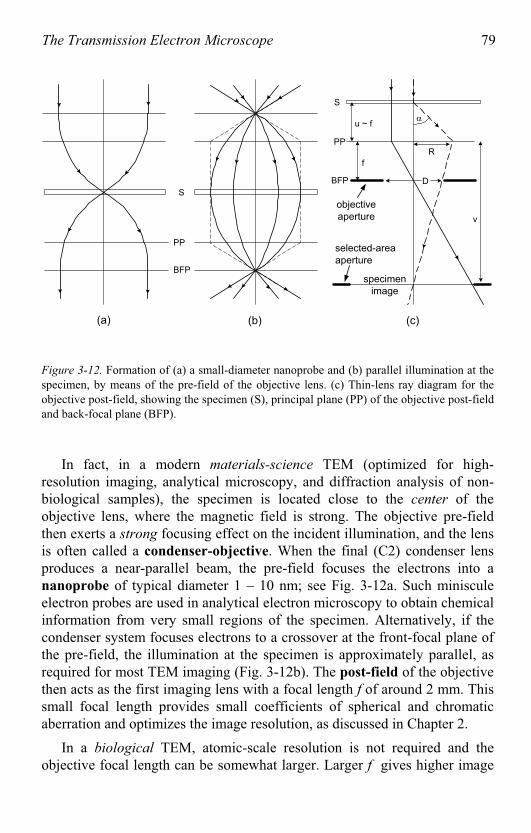
The Transmission Electron Microscope 79
(b)
S
BFP
PP
(c)
u ~ f
f
objective
aperture
specimen
image
R
D
v
(a)
S
BFP
PPselected-area
aperture
Figure 3-12. Formation of (a) a small-diameter nanoprobe and (b) parallel illumination at the specimen, by means of the pre-field of the objective lens. (c) Thin-lens ray diagram for theobjective post-field, showing the specimen (S), principal plane (PP) of the objective post-fieldand back-focal plane (BFP).
In fact, in a modern materials-science TEM (optimized for high-resolution imaging, analytical microscopy, and diffraction analysis of non-biological samples), the specimen is located close to the center of theobjective lens, where the magnetic field is strong. The objective pre-field then exerts a strong focusing effect on the incident illumination, and the lens is often called a condenser-objective. When the final (C2) condenser lensproduces a near-parallel beam, the pre-field focuses the electrons into a nanoprobe of typical diameter 1 – 10 nm; see Fig. 3-12a. Such minisculeelectron probes are used in analytical electron microscopy to obtain chemicalinformation from very small regions of the specimen. Alternatively, if thecondenser system focuses electrons to a crossover at the front-focal plane ofthe pre-field, the illumination at the specimen is approximately parallel, as required for most TEM imaging (Fig. 3-12b). The post-field of the objective then acts as the first imaging lens with a focal length f of around 2 mm. This small focal length provides small coefficients of spherical and chromaticaberration and optimizes the image resolution, as discussed in Chapter 2.
In a biological TEM, atomic-scale resolution is not required and the objective focal length can be somewhat larger. Larger f gives higher image
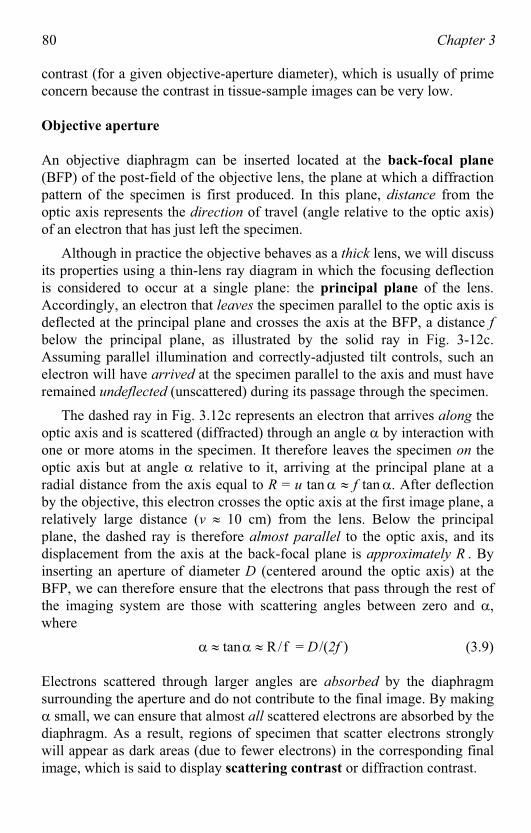
80 Chapter 3
contrast (for a given objective-aperture diameter), which is usually of primeconcern because the contrast in tissue-sample images can be very low.
Objective aperture
An objective diaphragm can be inserted located at the back-focal plane
(BFP) of the post-field of the objective lens, the plane at which a diffractionpattern of the specimen is first produced. In this plane, distance from the optic axis represents the direction of travel (angle relative to the optic axis) of an electron that has just left the specimen.
Although in practice the objective behaves as a thick lens, we will discussits properties using a thin-lens ray diagram in which the focusing deflection is considered to occur at a single plane: the principal plane of the lens. Accordingly, an electron that leaves the specimen parallel to the optic axis is deflected at the principal plane and crosses the axis at the BFP, a distance fbelow the principal plane, as illustrated by the solid ray in Fig. 3-12c.Assuming parallel illumination and correctly-adjusted tilt controls, such an electron will have arrived at the specimen parallel to the axis and must haverem ined undeflected (unscattered) during its passage through the specimen.a
The dashed ray in Fig. 3.12c represents an electron that arrives along theoptic axis and is scattered (diffracted) through an angle by interaction with one or more atoms in the specimen. It therefore leaves the specimen on theoptic axis but at angle relative to it, arriving at the principal plane at aradial distance from the axis equal to R = u tan f tan . After deflectionby the objective, this electron crosses the optic axis at the first image plane, arelatively large distance (v 10 cm) from the lens. Below the principal plane, the dashed ray is therefore almost parallel to the optic axis, and itsdisplacement from the axis at the back-focal plane is approximately R . By inserting an aperture of diameter D (centered around the optic axis) at the BFP, we can therefore ensure that the electrons that pass through the rest ofthe imaging system are those with scattering angles between zero and ,where
tan R/f = D /(2f ) (3.9)
Electrons scattered through larger angles are absorbed by the diaphragm surrounding the aperture and do not contribute to the final image. By making
small, we can ensure that almost all scattered electrons are absorbed by thediaphragm. As a result, regions of specimen that scatter electrons stronglywill appear as dark areas (due to fewer electrons) in the corresponding finalimage, which is said to display scattering contrast or diffraction contrast.
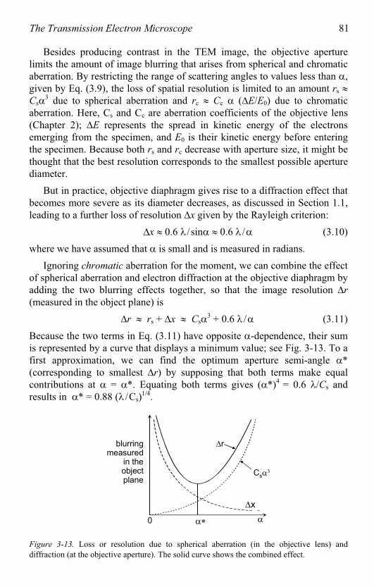
The Transmission Electron Microscope 81
Besides producing contrast in the TEM image, the objective aperture limits the amount of image blurring that arises from spherical and chromaticaberration. By restricting the range of scattering angles to values less than ,given by Eq. (3.9), the loss of spatial resolution is limited to an amount rs
Cs3 due to spherical aberration and rc Cc ( E/E0) due to chromatic
aberration. Here, Cs and Cc are aberration coefficients of the objective lens(Chapter 2); E represents the spread in kinetic energy of the electronsemerging from the specimen, and E0 is their kinetic energy before enteringthe specimen. Because both rs and rc decrease with aperture size, it might be thought that the best resolution corresponds to the smallest possible aperture dia eter.m
But in practice, objective diaphragm gives rise to a diffraction effect thatbecomes more severe as its diameter decreases, as discussed in Section 1.1, leading to a further loss of resolution x given by the Rayleigh criterion:
x 0.6 /sin 0.6 / (3.10)
where we have assumed that is small and is measured in radians.
Ignoring chromatic aberration for the moment, we can combine the effectof spherical aberration and electron diffraction at the objective diaphragm by adding the two blurring effects together, so that the image resolution r
(measured in the object plane) is
r rs + x Cs3 + 0.6 / (3.11)
Because the two terms in Eq. (3.11) have opposite -dependence, their sumis represented by a curve that displays a minimum value; see Fig. 3-13. To afirst approximation, we can find the optimum aperture semi-angle *(corresponding to smallest r) by supposing that both terms make equalcontributions at = *. Equating both terms gives ( *)4 = 0.6 /Cs and results in * = 0.88 ( /Cs)
1/4.
r
x
Cs
0
blurringmeasured
in theobjectplane
Figure 3-13. Loss or resolution due to spherical aberration (in the objective lens) anddiffraction (at the objective aperture). The solid curve shows the combined effect.
82 Chapter 3
A more correct procedure for finding the minimum is to differentiate r
with respect to and set the total derivative to zero, corresponding to zeroslope at the minimum of the curve, which gives: * = 0.67 ( /Cs)
1/4.
An even better procedure is to treat the blurring terms rs and x like statistical errors and combine their effect in quadrature:
( r)2 (rs)2 + ( x) 2 (Cs
3)2 + (0.6 / ) 2 (3.12)
Taking the derivative and setting it to zero then results in:
* = 0.63 ( /Cs)1/4 (3.13)
As an example, let us take E0 = 200 keV, so that = 2.5 pm, and Cs f /4 = 0.5 mm, as in Fig. 2-13. Then Eq. (3.13) gives * = 5.3 mrad, correspondingto an objective aperture of diameter D 2 *f 20 m. Using Eq.(3.12), theoptimum resolution is r* 0.29 nm.
Inclusion of chromatic aberration in Eq. (3.12) would decrease * a littleand increase r*. However, our entire procedure is somewhat pessimistic: itassumes that electrons are present in equal numbers at all scattering angles up to the aperture semi-angle . Also, a more exact treatment would bebased on wave optics rather than geometrical optics. In practice, a modern200 kV TEM can achieve a point resolution below 0.2 nm, allowing atomicresolution under suitable conditions, which include a low vibration level and low ambient ac magnetic field (Muller and Grazul, 2001). Nevertheless, our calculation has illustrated the importance of lens aberrations. Without these aberrations, large values of would be possible and the TEM resolution,limited only by Eq. (3.10), would (for sin 0.6) be x 0.025 nm,well below atomic dimensions.
In visible-light microscopy, lens aberrations can be made negligible. Glass lenses of large aperture can be used, such that sin approaches 1 andEq. (3.10) gives the resolution as x 300 nm as discussed in Chapter 1. Butas a result of the much smaller electron wavelength, the TEM resolution isbetter by more than a factor of 1000, despite the electron-lens aberrations.
Objective stigmator
The above estimates of resolution assume that the imaging system does not suffer from astigmatism. In practice, electrostatic charging of contaminationlayers (on the specimen or on an objective diaphragm) or hysteresis effectsin the lens polepieces give rise to axial astigmatism that may be different foreach specimen. The TEM operator can correct for axial astigmatism in theobjective (and other imaging lenses) using an objective stigmator located just below the objective lens. Obtaining the correct setting requires an adjustment
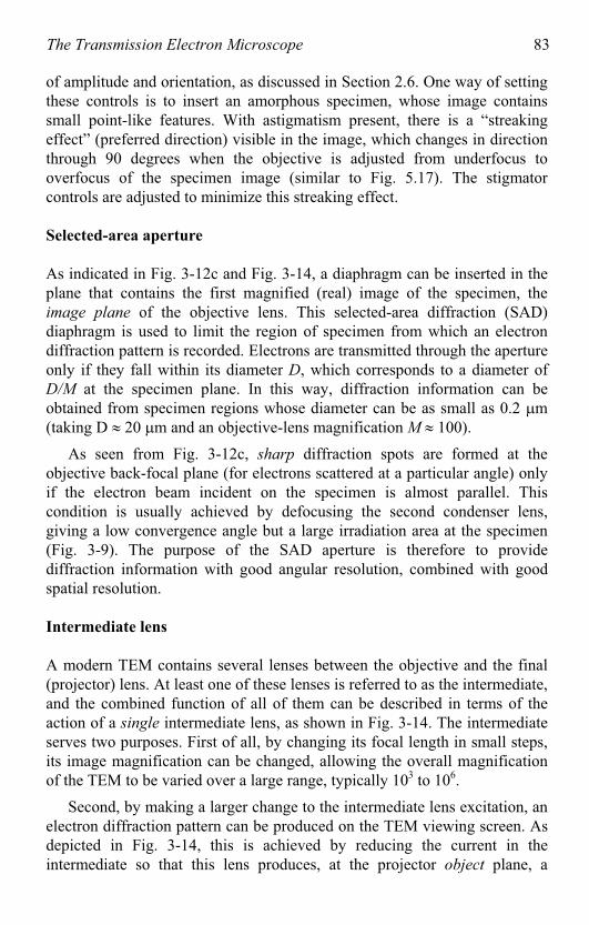
The Transmission Electron Microscope 83
of amplitude and orientation, as discussed in Section 2.6. One way of settingthese controls is to insert an amorphous specimen, whose image contains small point-like features. With astigmatism present, there is a “streaking effect” (preferred direction) visible in the image, which changes in direction through 90 degrees when the objective is adjusted from underfocus tooverfocus of the specimen image (similar to Fig. 5.17). The stigmatorcontrols are adjusted to minimize this streaking effect.
Selected-area aperture
As indicated in Fig. 3-12c and Fig. 3-14, a diaphragm can be inserted in theplane that contains the first magnified (real) image of the specimen, the image plane of the objective lens. This selected-area diffraction (SAD) diaphragm is used to limit the region of specimen from which an electrondiffraction pattern is recorded. Electrons are transmitted through the aperture only if they fall within its diameter D, which corresponds to a diameter ofD/M at the specimen plane. In this way, diffraction information can be obtained from specimen regions whose diameter can be as small as 0.2 m(taking D 20 m and an objective-lens magnification M 100).
As seen from Fig. 3-12c, sharp diffraction spots are formed at theobjective back-focal plane (for electrons scattered at a particular angle) only if the electron beam incident on the specimen is almost parallel. Thiscondition is usually achieved by defocusing the second condenser lens, giving a low convergence angle but a large irradiation area at the specimen(Fig. 3-9). The purpose of the SAD aperture is therefore to providediffraction information with good angular resolution, combined with goodspatial resolution.
Intermediate lens
A modern TEM contains several lenses between the objective and the final (projector) lens. At least one of these lenses is referred to as the intermediate,and the combined function of all of them can be described in terms of theaction of a single intermediate lens, as shown in Fig. 3-14. The intermediateserves two purposes. First of all, by changing its focal length in small steps,its image magnification can be changed, allowing the overall magnificationof the TEM to be varied over a large range, typically 103 to 106.
Second, by making a larger change to the intermediate lens excitation, anelectron diffraction pattern can be produced on the TEM viewing screen. As depicted in Fig. 3-14, this is achieved by reducing the current in theintermediate so that this lens produces, at the projector object plane, a
84 Chapter 3
diffraction pattern (solid ray crossing the optic axis) rather than an image ofthe specimen (dashed ray crossing the axis).
Because the objective lens reduces the angles of electrons relative to theoptic axis, intermediate-lens aberrations are not of great concern. Therefore,the intermediate can be operated as a weak lens (f several centimeters)without degrading the image or diffraction pattern.
specimen
objective
intermediate
lens(es)
projector
lens
viewing screen
objective
aperture
SAD
aperture
projector
object plane
Figure 3-14. Thin-lens ray diagram of the imaging system of a TEM. As usual, the imagerotation has been suppressed so that the electron optics can be represented on a flat plane.Image planes are represented by horizontal arrows and diffraction planes by horizontal dots. Rays that lead to a TEM-screen diffraction pattern are identified by the double arrowheads.(Note that the diagram is not to scale: the final image magnification is only 8 in this example).
The Transmission Electron Microscope 85
Projector lens
The purpose of the projector lens is to produce an image or a diffractionpattern across the entire TEM screen, with an overall diameter of severalcentimeters. Because of this requirement, some electrons (such as the solid single-arrow ray in Fig. 3-14) arrive at the screen at a large distance from theoptic axis, introducing the possibility of image distortion (Chapter 2). Tominimize this effect, the projector is designed to be a strong lens, with afocal length of a few millimeters. Ideally, the final-image diameter is fixed (the image should fill the TEM screen) and the projector operates at a fixed excitation, with a single object distance and magnification v/u 100.However, in many TEMs the projector-lens strength can be reduced in orderto give images of relatively low magnification (< 1000) on the viewing screen. As in the case of light optics, the final-image magnification is thealgebraic product of the magnification factors of each of the imaging lenses.
TEM screen and camera
A phosphor screen is used to convert the electron image to a visible form. It consists of a metal plate coated with a thin layer of powder that fluoresces (emits visible light) under electron bombardment. The traditional phosphormaterial is zinc sulfide (ZnS) with small amounts of metallic impurity added,although alternative phosphors are available with improved sensitivity (electron/photon conversion efficiency). The phosphor is chosen so that light is emitted in the middle of the spectrum (yellow-green region), to which the human eye is most sensitive. The TEM screen is used mainly for focusing a TEM image or diffraction pattern, and for this purpose, light-opticalbinoculars are often mounted just outside the viewing window, to providesome additional magnification. The viewing window is made of special glass(high lead content) and is of sufficient thickness to absorb the x-rays that areproduced when the electrons deposit their energy at the screen.
To permanently record a TEM image or diffraction pattern, photographicfilm can be used. This film has a layer of a silver halide (AgI and/or AgBr)emulsion, similar to that employed in black-and-white photography; bothelectrons and photons produce a subtle chemical change that can be amplified by immersion in a developer solution. In regions of high image intensity, the developer reduces the silver halide to metallic silver, whichappears dark. The recorded image is a therefore a photographic negative,whose contrast is reversed relative to the image seen on the TEM screen. An optical enlarger can be used to make a positive print on photographic paper, which also has a silver-halide coating.
86 Chapter 3
Nowadays, photographic film has been largely replaced by electronic image-recording devices, based on charge-coupled diode (CCD) sensors. They contain an array of a million or more silicon photodiodes, each of which provides an electrical signal proportional to the local intensity level. Because such devices are easily damaged by high-energy electrons, they are preceded by a phosphor screen that converts the electron image to variations in visible-light intensity. Electronic recording has numerous advantages. The recorded image can be inspected immediately on a monitor screen, avoidingthe delay (and cost) associated with photographic processing. Because the CCD sensitivity is high, even high-magnification (with low-intensity)images can be viewed without eyestrain, making focusing and astigmatism correction a lot easier. The image information is stored digitally in computermemory and subsequently on magnetic or optical disks, from which previousimages can be rapidly retrieved for comparison purposes. The digital nature of the image also allows various forms of image processing, as well as rapidtransfer of images between computers by means of the Internet.
Depth of focus and depth of field
As a matter of convenience, the film or CCD camera is located several centimeters below (or sometimes above) the TEM viewing screen. If a specimen image (or a diffraction pattern) has been brought to exact focus onthe TEM screen, it is strictly speaking out of focus at any other plane. At a plane that is a height h below (or above) the true image plane, each point inthe image becomes a circle of confusion whose radius is s = h tan , asillustrated in Fig. 3-15a. This radius is equivalent to a blurring:
s = s/M = (h/M) tan (3.14)
in the specimen plane, where M is the combined magnification of the entireimaging system and is the convergence angle at the screen, correspondingto scattering through an angle in the specimen, as shown in Fig. 3-15a.However, this blurring will be significant only if s is comparable to or greater that the resolution r of the in-focus TEM image. In other words, the additional image blurring will not be noticeable if s << r.
To compute s we first note, from trigonometry of the two large triangles in Fig. 3-15a, that x = u tan = v tan , giving tan = (u/v) tan = (1/M) tan .If an objective diaphragm is in place to remove electrons above 5 mrad,then tan /M = 5 10-6 rad for M = 1000, decreasing to 5 10-9 rad for M =106. These are extremely small angles, giving rise to correspondinglysmall values of s: for h = 10 cm, Eq. (3.14) gives s = 0.5 nm for M = 1000and s = 5 10-16 m for M = 106. Therefore, for typical TEM magnifications,the final image recorded at a different plane is equally sharp.
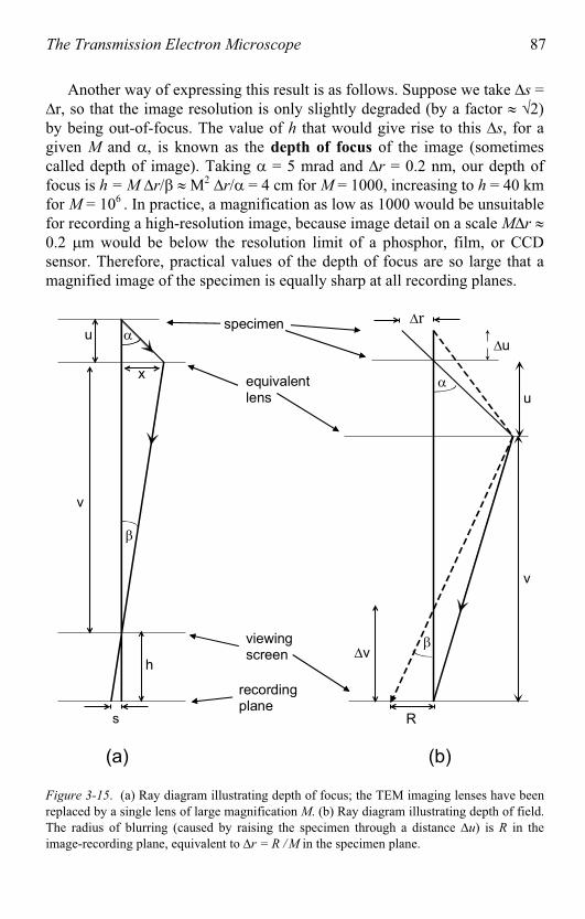
The Transmission Electron Microscope 87
Another way of expressing this result is as follows. Suppose we take s = r, so that the image resolution is only slightly degraded (by a factor 2)
by being out-of-focus. The value of h that would give rise to this s, for a given M and , is known as the depth of focus of the image (sometimescalled depth of image). Taking = 5 mrad and r = 0.2 nm, our depth of focus is h = M r/ M2 r/ = 4 cm for M = 1000, increasing to h = 40 km for M = 106 . In practice, a magnification as low as 1000 would be unsuitablefor recording a high-resolution image, because image detail on a scale M r
0.2 m would be below the resolution limit of a phosphor, film, or CCD sensor. Therefore, practical values of the depth of focus are so large that a magnified image of the specimen is equally sharp at all recording planes.
v
u
h
s
x
u
specimen
viewingscreen
recordingplane
equivalentlens u
(a) (b)
v
v
r
R
Figure 3-15. (a) Ray diagram illustrating depth of focus; the TEM imaging lenses have beenreplaced by a single lens of large magnification M. (b) Ray diagram illustrating depth of field.The radius of blurring (caused by raising the specimen through a distance u) is R in theimage-recording plane, equivalent to r = R /M in the specimen plane.
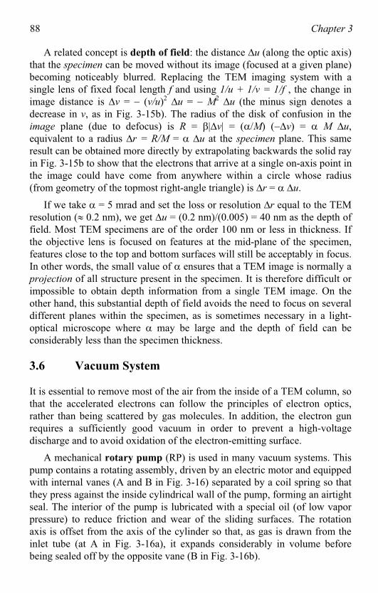
88 Chapter 3
A related concept is depth of field: the distance u (along the optic axis) that the specimen can be moved without its image (focused at a given plane)becoming noticeably blurred. Replacing the TEM imaging system with asingle lens of fixed focal length f and using 1/u + 1/v = 1/f , the change in image distance is v = (v/u)2 u = M2 u (the minus sign denotes a decrease in v, as in Fig. 3-15b). The radius of the disk of confusion in the image plane (due to defocus) is R = v = ( /M) ( v) = M u,equivalent to a radius r = R/M = u at the specimen plane. This sameresult can be obtained more directly by extrapolating backwards the solid rayin Fig. 3-15b to show that the electrons that arrive at a single on-axis point inthe image could have come from anywhere within a circle whose radius (from geometry of the topmost right-angle triangle) is r = u.
If we take = 5 mrad and set the loss or resolution r equal to the TEM resolution ( 0.2 nm), we get u = (0.2 nm)/(0.005) = 40 nm as the depth offield. Most TEM specimens are of the order 100 nm or less in thickness. Ifthe objective lens is focused on features at the mid-plane of the specimen,features close to the top and bottom surfaces will still be acceptably in focus. In other words, the small value of ensures that a TEM image is normally a projection of all structure present in the specimen. It is therefore difficult orimpossible to obtain depth information from a single TEM image. On theother hand, this substantial depth of field avoids the need to focus on severaldifferent planes within the specimen, as is sometimes necessary in a light-optical microscope where may be large and the depth of field can be considerably less than the specimen thickness.
3.6 Vacuum System
It is essential to remove most of the air from the inside of a TEM column, so that the accelerated electrons can follow the principles of electron optics, rather than being scattered by gas molecules. In addition, the electron gun requires a sufficiently good vacuum in order to prevent a high-voltagedischarge and to avoid oxidation of the electron-emitting surface.
A mechanical rotary pump (RP) is used in many vacuum systems. This pump contains a rotating assembly, driven by an electric motor and equipped with internal vanes (A and B in Fig. 3-16) separated by a coil spring so that they press against the inside cylindrical wall of the pump, forming an airtight seal. The interior of the pump is lubricated with a special oil (of low vapor pressure) to reduce friction and wear of the sliding surfaces. The rotation axis is offset from the axis of the cylinder so that, as gas is drawn from theinlet tube (at A in Fig. 3-16a), it expands considerably in volume before being sealed off by the opposite vane (B in Fig. 3-16b).
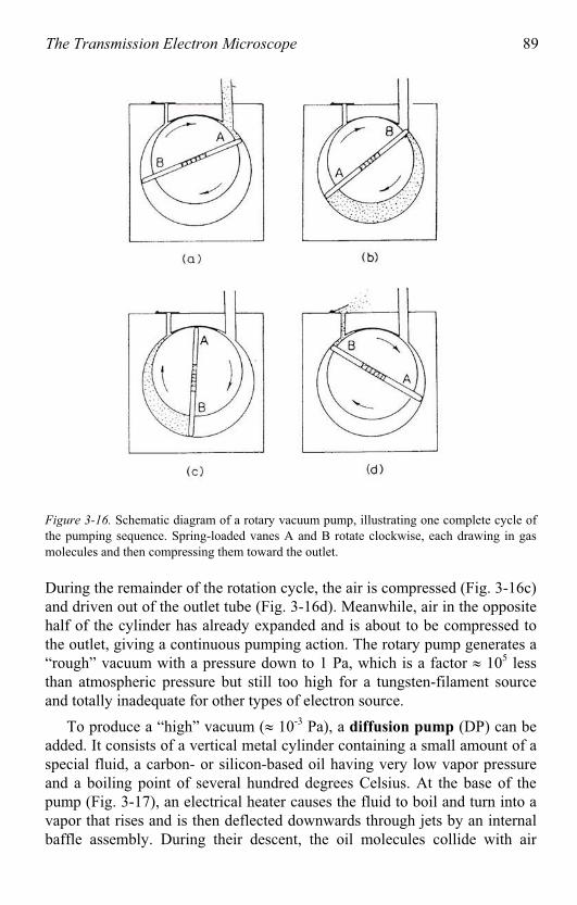
The Transmission Electron Microscope 89
Figure 3-16. Schematic diagram of a rotary vacuum pump, illustrating one complete cycle ofthe pumping sequence. Spring-loaded vanes A and B rotate clockwise, each drawing in gas molecules and then compressing them toward the outlet.
During the remainder of the rotation cycle, the air is compressed (Fig. 3-16c) and driven out of the outlet tube (Fig. 3-16d). Meanwhile, air in the opposite half of the cylinder has already expanded and is about to be compressed to the outlet, giving a continuous pumping action. The rotary pump generates a “rough” vacuum with a pressure down to 1 Pa, which is a factor 105 lessthan atmospheric pressure but still too high for a tungsten-filament source and totally inadequate for other types of electron source.
To produce a “high” vacuum ( 10-3 Pa), a diffusion pump (DP) can be added. It consists of a vertical metal cylinder containing a small amount of a special fluid, a carbon- or silicon-based oil having very low vapor pressure and a boiling point of several hundred degrees Celsius. At the base of the pump (Fig. 3-17), an electrical heater causes the fluid to boil and turn into a vapor that rises and is then deflected downwards through jets by an internalbaffle assembly. During their descent, the oil molecules collide with air
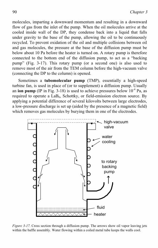
90 Chapter 3
molecules, imparting a downward momentum and resulting in a downwardflow of gas from the inlet of the pump. When the oil molecules arrive at thecooled inside wall of the DP, they condense back into a liquid that fallsunder gravity to the base of the pump, allowing the oil to be continuouslyrecycled. To prevent oxidation of the oil and multiple collisions between oil and gas molecules, the pressure at the base of the diffusion pump must bebelow about 10 Pa before the heater is turned on. A rotary pump is therefore connected to the bottom end of the diffusion pump, to act as a “backing pump” (Fig. 3-17). This rotary pump (or a second one) is also used to remove most of the air from the TEM column before the high-vacuum valve (connecting the DP to the column) is opened.
Sometimes a tubomolecular pump (TMP), essentially a high-speedturbine fan, is used in place of (or to supplement) a diffusion pump. Usuallyan ion pump (IP in Fig. 3-18) is used to achieve pressures below 10-4 Pa, as required to operate a LaB6, Schottky, or field-emission electron source. Byapplying a potential difference of several kilovolts between large electrodes,a low-pressure discharge is set up (aided by the presence of a magnetic field) which removes gas molecules by burying them in one of the electrodes.
fluid
heater
water
cooling
to rotary
backing
pump
high-vacuum
valve
Figure 3-17. Cross section through a diffusion pump. The arrows show oil vapor leaving jetswithin the baffle assembly. Water flowing within a coiled metal tube keeps the walls cool.
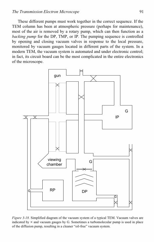
The Transmission Electron Microscope 91
These different pumps must work together in the correct sequence. If the TEM column has been at atmospheric pressure (perhaps for maintenance),most of the air is removed by a rotary pump, which can then function as a backing pump for the DP, TMP, or IP. The pumping sequence is controlledby opening and closing vacuum valves in response to the local pressure,monitored by vacuum gauges located in different parts of the system. In a modern TEM, the vacuum system is automated and under electronic control; in fact, its circuit board can be the most complicated in the entire electronicsof the microscope.
DPRP
viewing
chamber
gun
IP
G
G
G
G
Figure 3-18. Simplified diagram of the vacuum system of a typical TEM. Vacuum valves areindicated by and vacuum gauges by G. Sometimes a turbomolecular pump is used in placeof the diffusion pump, resulting in a cleaner “oil-free” vacuum system.
92 Chapter 3
Frequently, liquid nitrogen is used to help in achieving adequate vacuuminside the TEM, through a process known as cryopumping. With a boilingpoint of 77 K, liquid nitrogen can cool internal surfaces sufficiently to cause water vapor and organic vapors (hydrocarbons) to condense onto the surface. These vapors are therefore removed from the vacuum, so long as the surfaceremains cold. In a diffusion-pumped vacuum system, liquid nitrogen is often poured into a container (known as a trap) above the DP to minimize“backstreaming” of diffusion-pump vapor into the TEM column.
Organic vapors can also enter the vacuum from components such as the rubber o-ring seals. When a surface is irradiated with electrons, hydrocarbon molecules that arrive at the surface can become chemically bonded together to form a solid polymer. This electron-beam contamination may occur on both the top and bottom surfaces of a TEM specimen; the resulting contamination layers cause additional scattering of the electrons, reducing the contrast of the TEM image. To combat this process, liquid nitrogen is added to a decontaminator trap attached to the side of the TEM column. By conduction through metal rods or braiding, it cools metal plates located just above or below the specimen, thereby condensing water and organic vapors and giving a low partial pressure of these components in the immediatevicinity of the specimen.
Chapter 4
TEM SPECIMENS AND IMAGES
In the transmitted-light microscope, variation of intensity within an image is caused by differences in the absorption of photons within different regionsof the specimen. In the case of a TEM, however, essentially all of the incoming electrons are transmitted through the specimen, provided it is suitably thin. Although not absorbed, these electrons are scattered (deflectedin their path) by the atoms of the specimen. To understand the formation andinterpretation of TEM images, we need to examine the nature of thiscattering process.s
Many of the concepts involved can be understood by considering just asingle “target” atom, which we represent in the simplest way as a centralnucleus surrounded by orbiting particles, the atomic electrons; see Fig. 4-1. This is the classical planetary model, first established by Ernest Rutherford from analysis of the scattering of alpha particles. In fact, our analysis will largely follow that of Rutherford. Instead of positive alpha particles, we havenegative incident electrons, but the cause of the scattering remains the same,namely the electrostatic (Coulomb) interaction between charged particles.
Interaction between the incoming fast electron and an atomic nucleus
gives rise to elastic scattering where (as we will see) almost no energy istransferred. Interaction between the fast electron and atomic electrons results in inelastic scattering, in which process the transmitted electron can lose anappreciable amount of energy. We will consider these two types of event inturn, dealing first with the kinematics of scattering, where we consider the momentum and energy of the fast electron, without needing to know the nature of the forces involved. As the nature of the force does not matter, the kinematics of electron scattering employs the same principles of classicalmechanics as are used to treat the collision of larger (macroscopic) objects.
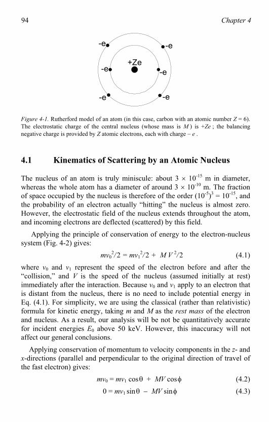
94 Chapter 4
+Ze
-e -e
-e-e
-e-e
Figure 4-1. Rutherford model of an atom (in this case, carbon with an atomic number Z = 6). The electrostatic charge of the central nucleus (whose mass is M ) is +Ze ; the balancingnegative charge is provided by Z atomic electrons, each with charge e .
4.1 Kinematics of Scattering by an Atomic Nucleus
The nucleus of an atom is truly miniscule: about 3 10-15 m in diameter,whereas the whole atom has a diameter of around 3 10-10 m. The fraction of space occupied by the nucleus is therefore of the order (10-5)3 = 10-15, and the probability of an electron actually “hitting” the nucleus is almost zero.However, the electrostatic field of the nucleus extends throughout the atom,and incoming electrons are deflected (scattered) by this field.
Applying the principle of conservation of energy to the electron-nucleus system (Fig. 4-2) gives:
mv02/2 = mv1
2/2 + M V 2/2 (4.1)
where v0 and v1 represent the speed of the electron before and after the“collision,” and V is the speed of the nucleus (assumed initially at rest) immediately after the interaction. Because v0 and v1 apply to an electron that is distant from the nucleus, there is no need to include potential energy in Eq. (4.1). For simplicity, we are using the classical (rather than relativistic) formula for kinetic energy, taking m and M as the rest mass of the electronand nucleus. As a result, our analysis will be not be quantitatively accuratefor incident energies E0 above 50 keV. However, this inaccuracy will notffect our general conclusions.a
Applying conservation of momentum to velocity components in the z- andx-directions (parallel and perpendicular to the original direction of travel ofhe fast electron) gives: t
mv0 = mv1 cos + MV cos (4.2)
0 = mv1 sin MV sin (4.3)
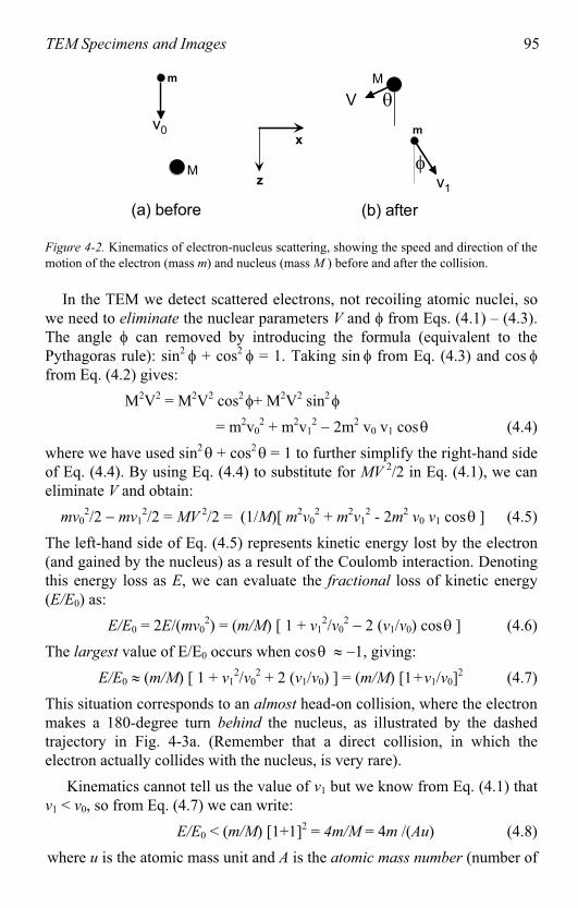
TEM Specimens and Images 95
(a) before (b) after
M
m
m
M
z
x
V
v1
v0
Figure 4-2. Kinematics of electron-nucleus scattering, showing the speed and direction of themotion of the electron (mass m) and nucleus (mass M ) before and after the collision.
In the TEM we detect scattered electrons, not recoiling atomic nuclei, sowe need to eliminate the nuclear parameters V and from Eqs. (4.1) – (4.3). The angle can removed by introducing the formula (equivalent to the Pythagoras rule): sin2 + cos2 = 1. Taking sin from Eq. (4.3) and cosrom Eq. (4.2) gives: f
M2V2 = M2V2 cos2 + M2V2 sin2
= m2v02 + m2v1
2 2m2 v0 v1 cos (4.4)
where we have used sin2 + cos2 = 1 to further simplify the right-hand side of Eq. (4.4). By using Eq. (4.4) to substitute for MV 2/2 in Eq. (4.1), we canliminate V and obtain: e
mv02/2 mv1
2/2 = MV 2/2 = (1/M)[ m2v02 + m2v1
2 - 2m2 v0 v1 cos ] (4.5)
The left-hand side of Eq. (4.5) represents kinetic energy lost by the electron (and gained by the nucleus) as a result of the Coulomb interaction. Denotingthis energy loss as E, we can evaluate the fractional loss of kinetic energy E/E0) as: (
E/E0 = 2E/(mv02) = (m/M) [ 1 + v1
2/v02 2 (v1/v0) cos ] (4.6)
The largest value of E/E0 occurs when cos 1, giving:
E/E0 (m/M) [ 1 + v12/v0
2 + 2 (v1/v0) ] = (m/M) [1+v1/v0]2 (4.7)
This situation corresponds to an almost head-on collision, where the electronmakes a 180-degree turn behind the nucleus, as illustrated by the dashed trajectory in Fig. 4-3a. (Remember that a direct collision, in which the electron actually collides with the nucleus, is very rare).
Kinematics cannot tell us the value of v1 but we know from Eq. (4.1) thatv1 < v0, so from Eq. (4.7) we can write:
E/E0 < (m/M) [1+1]2 = 4m/M = 4m /(Au) (4.8)
where u is the atomic mass unit and A is the atomic mass number (number of
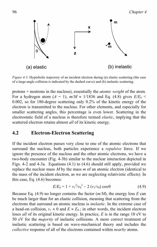
96 Chapter 4
(b) inelastic
m
(a) elastic
m
z
x
Figure 4-3. Hyperbolic trajectory of an incident electron during (a) elastic scattering (the case of a large-angle collision is indicated by the dashed curve) and (b) inelastic scattering.
protons + neutrons in the nucleus), essentially the atomic weight of the atom.For a hydrogen atom (A = 1), m/M 1/1836 and Eq. (4.8) gives E/E0 < 0.002, so for 180-degree scattering only 0.2% of the kinetic energy of theelectron is transmitted to the nucleus. For other elements, and especially forsmaller scattering angles, this percentage is even lower. Scattering in theelectrostatic field of a nucleus is therefore termed elastic, implying that the scattered electron retains almost all of its kinetic energy.
4.2 Electron-Electron Scattering
If the incident electron passes very close to one of the atomic electrons that surround the nucleus, both particles experience a repulsive force. If we ignore the presence of the nucleus and the other atomic electrons, we have a two-body encounter (Fig. 4-3b) similar to the nuclear interaction depicted in Figs. 4-2 and 4-3a. Equations (4.1) to (4.6) should still apply, provided wereplace the nuclear mass M by the mass m of an atomic electron (identical to the mass of the incident electron, as we are neglecting relativistic effects). In his case, Eq. (4.6) becomes:t
E/E0 = 1 + v12/v0
2 2 (v1/v0) cos (4.9)
Because Eq. (4.9) no longer contains the factor (m/M), the energy loss E canbe much larger than for an elastic collision, meaning that scattering from the electrons that surround an atomic nucleus is inelastic. In the extreme case ofa head-on collision, v1 0 and E E0 ; in other words, the incident electronloses all of its original kinetic energy. In practice, E is in the range 10 eV to50 eV for the majority of inelastic collisions. A more correct treatment of inelastic scattering is based on wave-mechanical theory and includes the ollective response of all of the electrons contained within nearby atoms.c
TEM Specimens and Images 97
In practice, an electron traveling through a solid must experience both repulsive forces (from other electrons) and attractive forces (from atomicnuclei). But in scattering theory, it turns out to be justified to imagine thateither one or the other effect predominates, and to divide the scattering that occurs into elastic and inelastic components.
4.3 The Dynamics of Scattering
Because the force acting on a moving electron is electrostatic, its magnitudeF is described by Coulomb’s law. So for elastic scattering of the electron by he electrostatic field of a single nucleus: t
F = K (e)(Ze) /r 2 (4.10)
where K = 1/(4 0) = 9.0 109 Nm2C-2 is the Coulomb constant. ApplyingNewtonian mechanics (F = ma) to this problem, the electron trajectory can be shown to be a hyperbola, as depicted in Fig. 4-3a.
The angular distribution of elastic scattering can be expressed in termsof a probability P( ) for an electron to be scattered through a given angle .But to understand TEM contrast, we are more interested in the probabilityP(> ) that an electron is scattered through an angle that exceeds the semi-angle of the objective aperture. Such an electron will be absorbed within the diaphragm material that surrounds the aperture, resulting in a reduction in intensity within the TEM image.
We can think of the nucleus as presenting (to each incident electron) a target of area , known as a scattering cross section. Atoms being round,this target takes the form of a disk of radius a and of area = a2. An electron is scattered through an angle that exceeds the aperture semi-angle
only if it arrives at a distance less than a from the nucleus, a being afunction of . But relative to any given nucleus, electrons arrive randomly
with various values of the impact parameter b, defined as the distance of closest approach if we neglect the hyperbolic curvature of the trajectory, as shown in Fig. 4-4. So if b < a, the electron is scattered through an angle greater than and is subsequently absorbed by the objective diaphragm.
By how much the scattering angle exceeds depends on just how close the electron passes to the center of the atom: small b leads to large and vice
versa. Algebraic analysis of the force and velocity components, making useof Eq. (4.7) and Newton's second law of motion (see Appendix), gives:
K Z e2/(E0 b) (4.11)
Equation (4.11) specifies an inverse relation between b and , as expectedbecause electrons with a smaller impact parameter pass closer to the nucleus,
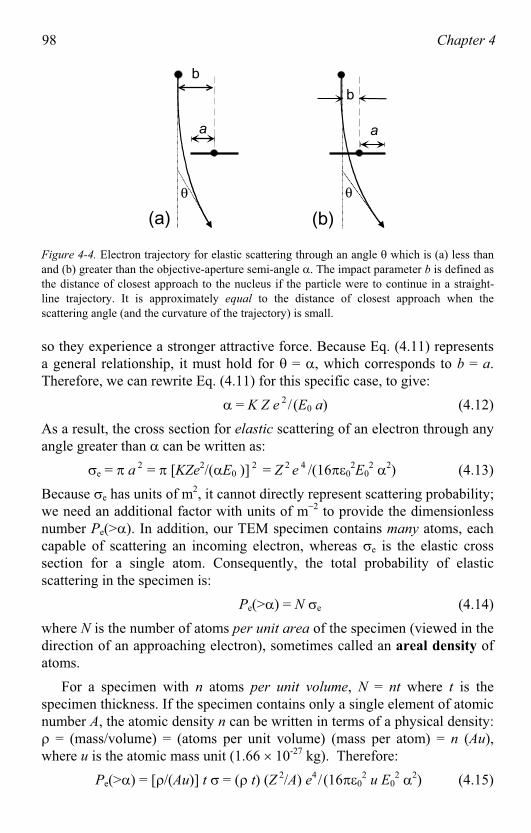
98 Chapter 4
a
b
a
b
(a) (b)
Figure 4-4. Electron trajectory for elastic scattering through an angle which is (a) less thanand (b) greater than the objective-aperture semi-angle . The impact parameter b is defined asthe distance of closest approach to the nucleus if the particle were to continue in a straight-line trajectory. It is approximately equal to the distance of closest approach when the scattering angle (and the curvature of the trajectory) is small.
so they experience a stronger attractive force. Because Eq. (4.11) representsa general relationship, it must hold for = , which corresponds to b = a.Therefore, we can rewrite Eq. (4.11) for this specific case, to give:
= K Z e 2 / (E0 a) (4.12)
As a result, the cross section for elastic scattering of an electron through anyngle greater than can be written as: a
e = a 2 = [KZe2/( E0 )] 2 = Z 2 e 4 /(16 0
2E02 2) (4.13)
Because e has units of m2, it cannot directly represent scattering probability;we need an additional factor with units of m 2 to provide the dimensionless number Pe(> ). In addition, our TEM specimen contains many atoms, eachcapable of scattering an incoming electron, whereas e is the elastic crosssection for a single atom. Consequently, the total probability of elasticcattering in the specimen is: s
Pe(> ) = N e (4.14)
where N is the number of atoms per unit area of the specimen (viewed in the direction of an approaching electron), sometimes called an areal density of toms.a
For a specimen with n atoms per unit volume, N = nt where t is the specimen thickness. If the specimen contains only a single element of atomicnumber A, the atomic density n can be written in terms of a physical density:
= (mass/volume) = (atoms per unit volume) (mass per atom) = n (Au),where u is the atomic mass unit (1.66 10-27 kg). Therefore:
Pe(> ) = [ /(Au)] t = ( t) (Z 2/A) e4 /(16 02 u E0
2 2) (4.15)
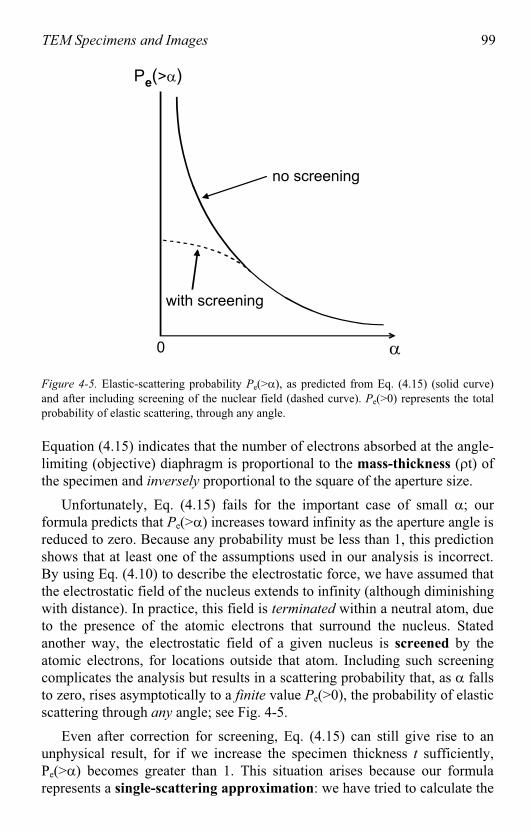
TEM Specimens and Images 99
Pe(> )
with screening
no screening
0
Figure 4-5. Elastic-scattering probability Pe(> ), as predicted from Eq. (4.15) (solid curve) and after including screening of the nuclear field (dashed curve). Pe(>0) represents the totalprobability of elastic scattering, through any angle.
Equation (4.15) indicates that the number of electrons absorbed at the angle-limiting (objective) diaphragm is proportional to the mass-thickness ( t) of he specimen and inversely proportional to the square of the aperture size. t
Unfortunately, Eq. (4.15) fails for the important case of small ; ourformula predicts that Pe(> ) increases toward infinity as the aperture angle isreduced to zero. Because any probability must be less than 1, this prediction shows that at least one of the assumptions used in our analysis is incorrect.By using Eq. (4.10) to describe the electrostatic force, we have assumed thatthe electrostatic field of the nucleus extends to infinity (although diminishingwith distance). In practice, this field is terminated within a neutral atom, due to the presence of the atomic electrons that surround the nucleus. Statedanother way, the electrostatic field of a given nucleus is screened by the atomic electrons, for locations outside that atom. Including such screening complicates the analysis but results in a scattering probability that, as falls to zero, rises asymptotically to a finite value Pe(>0), the probability of elastic cattering through any angle; see Fig. 4-5. s
Even after correction for screening, Eq. (4.15) can still give rise to an unphysical result, for if we increase the specimen thickness t sufficiently,Pe(> ) becomes greater than 1. This situation arises because our formularepresents a single-scattering approximation: we have tried to calculate the
100 Chapter 4
fraction of electrons that are scattered only once in a specimen. For very thinspecimens, this fraction increases in proportion to the specimen thickness, asimplied by Eq. (4.15). But in thicker specimens, the probability of single scattering must decrease with increasing thickness because most electronsbecome scattered several times. If we use Poisson statistics to calculate theprobability Pn of n-fold scattering, each probability comes out less than 1, as expected. In fact, the sum Pn over all n (including n = 0) is equal to 1, as would be expected because all electrons are transmitted (except forpecimens that are far too thick for transmission microscopy).s
The above arguments can be repeated for the case of inelastic scattering,taking the electrostatic force as F = K(e)(e)/r2 because the incident electron is now scattered by an atomic electron rather than by the nucleus. The result is an equation similar to Eq. (4.15) but with the factor Z 2 missing. However, this result would apply to inelastic scattering by only a single atomicelectron. Considering all Z electrons within the atom, the inelastic-scatteringprobability must be multiplied by Z, giving:
Pi(> ) = ( t) (Z/A) e4 /(16 02 u E0
2 2) (4.16)
Comparison of Eq. (4.16) with Eq. (4.15) shows that the amount of inelastic cattering, relative to elastic scattering, is s
Pi(> ) /Pe(> ) = 1/Z (4.17)
Equation (4.17) predicts that inelastic scattering makes a relatively smallcontribution for most elements. However, it is based on Eq. (4.15), which isaccurate only for larger aperture angles. For small , where screening of the nuclear field reduces the amount of elastic scattering, the inelastic/elasticratio is much higher. More accurate theory (treating the incoming electronsas waves) and experimental measurements of the scattering show that Pe(>0)is typically proportional to Z 1.5 (rather than Z 2 ), that Pi(>0) is proportionalo Z 0.5 (rather than Z ) and that, considering scattering through all angles,t
Pi(>0)/Pe(>0) 20/Z (4.18)
Consequently, inelastic scattering makes a significant contribution to theotal scattering (through any angle) in the case of light (low-Z) elements.t
Although our classical-physics analysis turns out to be rather inaccurate in predicting absolute scattering probabilities, the thickness and materialparameters involved in Eq. (4.15) and Eq. (4.16) do provide a reasonableexplanation for the contrast (variation in intensity level) in TEM imagesobtained from non-crystalline (amorphous) specimens such as glasses, certain kinds of polymers, amorphous thin films, and most types of biological material.
TEM Specimens and Images 101
4.4 Scattering Contrast from Amorphous Specimens
Most TEM images are viewed and recorded with an objective aperture(diameter D) inserted and centered about the optic axis of the TEM objective lens (focal length f ). As represented by Eq. (3.9), this aperture absorbselectrons that are scattered through an angle greater than 0.5D/f.However, any part of the field of view that contains no specimen (such as a hole or a region beyond the specimen edge) is formed from electrons that remain unscattered, so that part appears bright relative to the specimen. As a esult, this central-aperture image is referred to as a bright-field image. r
Biological tissue, at least in its dry state, is mainly carbon and so, for this common type of specimen, we can take Z = 6, A = 12, and 2 g/cm2 = 2000 kg/m3. For a biological TEM, typical parameters are E0 = 100 keV = 1.6 10-14 J and 0.5D/f = 10 mrad = 0.01 rad, taking an objective-lensfocal length f = 2 mm and objective-aperture diameter D = 40 m. With these values, Eq. (4.15) gives Pe( ) 0.47 for a specimen thickness of t = 20 nm. The same parameters inserted into Eq.(4.16) give Pi(> ) 0.08, and thetotal fraction of electrons that are absorbed by the objective diaphragm is
(>10 mrad) 0.47 + 0.08 = 0.54 . P
We therefore predict that more than half of the transmitted electrons are intercepted by a typical-size objective aperture, even for a very thin (20 nm)specimen. This fraction might be even larger for a thicker specimen, but our single-scattering approximation would not be valid. In practice, the specimenthickness must be less than about 200 nm, assuming an accelerating potential of 100 kV and a specimen consisting mainly of low-Z elements. If the specimen is appreciably thicker, only a small fraction of the transmittedelectrons pass through the objective aperture, and the bright-field image is ver dim on the TEM screen.y
Because (A/Z) is approximately the same ( 2) for all elements, Eq. (4.16)indicates that Pi(> ) increases only slowly with increasing atomic number,due to the density term , which tends to increase with increasing Z. Butusing the same argument, Eq. (4.15) implies that Pe(> ) is approximatelyproportional to Z. Therefore specimens that contain mainly heavy elementsscatter electrons more strongly and would have to be even thinner, placing unrealistic demands on the specimen preparation. Such specimens areusually examined in a “materials science” TEM that employs an acceleratingvoltage of 200 kV or higher, taking advantage of the reduction in e and Pe
with increasing E0; see Eqs. (4.13) and (4.15).
For imaging non-crystalline specimens, the main purpose of the objectiveaperture is to provide scattering contrast in the TEM image of a specimen
102 Chapter 4
whose composition or thickness varies between different regions. Thickerregions of the sample scatter a higher fraction of the incident electrons, manyof which are absorbed by the objective diaphragm, so that the corresponding
regions in the image appear dark, giving rise to thickness contrast in theimage. Regions of higher atomic number also appear dark relative to their surroundings, due mainly to an increase in the amount of elastic scattering,as shown by Eq. (4.15), giving atomic-number contrast (Z-contrast). Takentogether, these two effects are often described as mass-thickness contrast.They provide the information content of TEM images of amorphousmaterials, in which the atoms are arranged more-or-less randomly (not in a regular array, as in a crystal), as illustrated by the following examples.
Stained biological tissue
TEM specimens of biological (animal or plant) tissue are made by cutting very thin slices (sections) from a small block of embedded tissue (held together by epoxy glue) using an instrument called an ultramicrotome that employs a glass or diamond knife as the cutting blade. To prevent the sections from curling up, they are floated onto a water surface, whichsupports them evenly by surface tension. A fine-mesh copper grid (3-mmdiameter, held at its edge by tweezers) is then introduced below the watersurface and slowly raised, leaving the tissue section supported by the grid.After drying in air, the tissue remains attached to the grid by local
echanical and chemical forces.m
Tissue sections prepared in this way are fairly uniform in thickness, therefore almost no contrast arises from the thickness term in Eq. (4.15). Their atomic number also remains approximately constant (Z 6 for drytissue), so the overall contrast is very low and the specimen appearsfeatureless in the TEM. To produce scattering contrast, the sample ischemically treated by a process called staining. Before or after slicing, thetissue is immersed in a solution that contains a heavy (high-Z) metal. The solution is absorbed non-uniformly by the tissue; a positive stain, such as lead citrate or uranyl acetate, tends to migrate to structural features organelles) within each cell.(
As illustrated in Fig. 4-6, these regions appear dark in the TEM imagebecause Pb or U atoms strongly scatter the incident electrons, and most ofthe scattered electrons are absorbed by the objective diaphragm. A negative
stain (such as phosphotungstic acid) tends to avoid cellular structures, whichin the TEM image appear bright relative to their surroundings, as they contain fewer tungsten atoms.
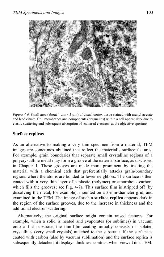
TEM Specimens and Images 103
Figure 4-6. Small area (about 4 m 3 m) of visual cortex tissue stained with uranyl acetateand lead citrate. Cell membranes and components (organelles) within a cell appear dark due to elastic scattering and subsequent absorption of scattered electrons at the objective aperture.
Surface replicas
As an alternative to making a very thin specimen from a material, TEMimages are sometimes obtained that reflect the material’s surface features.For example, grain boundaries that separate small crystalline regions of apolycrystalline metal may form a groove at the external surface, as discussedin Chapter 1. These grooves are made more prominent by treating the material with a chemical etch that preferentially attacks grain-boundaryregions where the atoms are bonded to fewer neighbors. The surface is thencoated with a very thin layer of a plastic (polymer) or amorphous carbon,which fills the grooves; see Fig. 4-7a. This surface film is stripped off (by dissolving the metal, for example), mounted on a 3-mm-diameter grid, andexamined in the TEM. The image of such a surface replica appears dark in the region of the surface grooves, due to the increase in thickness and thedditional electron scattering.a
Alternatively, the original surface might contain raised features. Forexample, when a solid is heated and evaporates (or sublimes) in vacuum onto a flat substrate, the thin-film coating initially consists of isolated crystallites (very small crystals) attached to the substrate. If the surface iscoated with carbon (also by vacuum sublimation) and the surface replica is subsequently detached, it displays thickness contrast when viewed in a TEM.
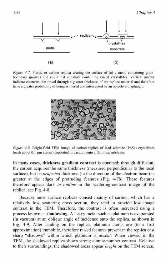
104 Chapter 4
replica
(a) (b)
metal substrate
crystallites
Figure 4-7. Plastic or carbon replica coating the surface of (a) a metal containing grain-boundary grooves and (b) a flat substrate containing raised crystallites. Vertical arrowsindicate electrons that travel through a greater thickness of the replica material and thereforehave a greater probability of being scattered and intercepted by an objective diaphragm.
Figure 4-8. Bright-field TEM image of carbon replica of lead selenide (PbSe) crystallites(each about 0.1 m across) deposited in vacuum onto a flat mica substrate.
In many cases, thickness gradient contrast is obtained: through diffusion,the carbon acquires the same thickness (measured perpendicular to the local surface), but its projected thickness (in the direction of the electron beam) isgreater at the edges of protruding features (Fig. 4-7b). These featurestherefore appear dark in outline in the scattering-contrast image of theeplica; see Fig. 4-8. r
Because most surface replicas consist mainly of carbon, which has a relatively low scattering cross section, they tend to provide low imagecontrast in the TEM. Therefore, the contrast is often increased using aprocess known as shadowing. A heavy metal such as platinum is evaporated(in vacuum) at an oblique angle of incidence onto the replica, as shown inFig. 4-9. After landing on the replica, platinum atoms are (to a first approximation) immobile, therefore raised features present in the replica castsharp “shadows” within which platinum is absent. When viewed in theTEM, the shadowed replica shows strong atomic-number contrast. Relativeto their surroundings, the shadowed areas appear bright on the TEM screen,
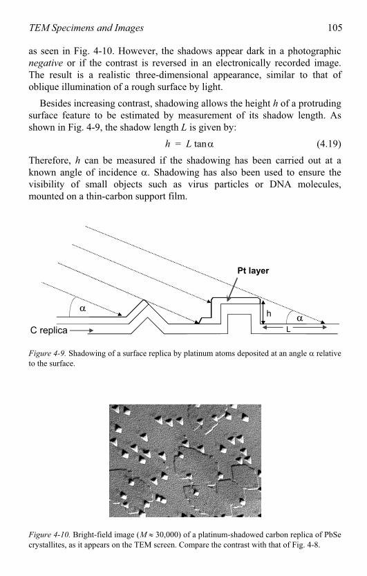
TEM Specimens and Images 105
as seen in Fig. 4-10. However, the shadows appear dark in a photographic negative or if the contrast is reversed in an electronically recorded image. The result is a realistic three-dimensional appearance, similar to that of oblique illumination of a rough surface by light.
Besides increasing contrast, shadowing allows the height h of a protrudingsurface feature to be estimated by measurement of its shadow length. As shown in Fig. 4-9, the shadow length L is given by:
h = L tan (4.19)
Therefore, h can be measured if the shadowing has been carried out at a known angle of incidence . Shadowing has also been used to ensure thevisibility of small objects such as virus particles or DNA molecules,mounted on a thin-carbon support film.
C replica
Pt layer
L
h
Figure 4-9. Shadowing of a surface replica by platinum atoms deposited at an angle relativeto the surface.
Figure 4-10. Bright-field image (M 30,000) of a platinum-shadowed carbon replica of PbSecrystallites, as it appears on the TEM screen. Compare the contrast with that of Fig. 4-8.
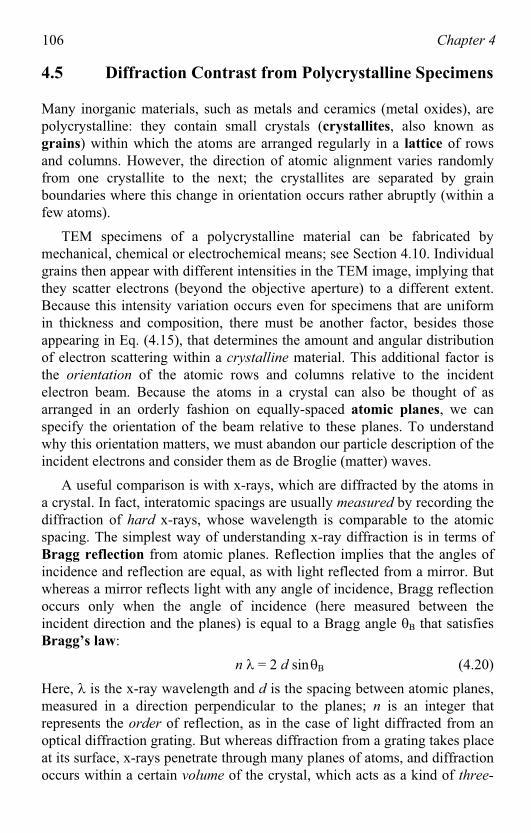
106 Chapter 4
4.5 Diffraction Contrast from Polycrystalline Specimens
Many inorganic materials, such as metals and ceramics (metal oxides), arepolycrystalline: they contain small crystals (crystallites, also known asgrains) within which the atoms are arranged regularly in a lattice of rows and columns. However, the direction of atomic alignment varies randomlyfrom one crystallite to the next; the crystallites are separated by grainboundaries where this change in orientation occurs rather abruptly (within afew atoms).
TEM specimens of a polycrystalline material can be fabricated bymechanical, chemical or electrochemical means; see Section 4.10. Individualgrains then appear with different intensities in the TEM image, implying that they scatter electrons (beyond the objective aperture) to a different extent.Because this intensity variation occurs even for specimens that are uniformin thickness and composition, there must be another factor, besides thoseappearing in Eq. (4.15), that determines the amount and angular distributionof electron scattering within a crystalline material. This additional factor isthe orientation of the atomic rows and columns relative to the incident electron beam. Because the atoms in a crystal can also be thought of asarranged in an orderly fashion on equally-spaced atomic planes, we canspecify the orientation of the beam relative to these planes. To understand why this orientation matters, we must abandon our particle description of the incident electrons and consider them as de Broglie (matter) waves.
A useful comparison is with x-rays, which are diffracted by the atoms ina crystal. In fact, interatomic spacings are usually measured by recording thediffraction of hard x-rays, whose wavelength is comparable to the atomicspacing. The simplest way of understanding x-ray diffraction is in terms of Bragg reflection from atomic planes. Reflection implies that the angles of incidence and reflection are equal, as with light reflected from a mirror. Butwhereas a mirror reflects light with any angle of incidence, Bragg reflectionoccurs only when the angle of incidence (here measured between the incident direction and the planes) is equal to a Bragg angle B that satisfiesBragg’s law:
n = 2 d sin B (4.20)
Here, is the x-ray wavelength and d is the spacing between atomic planes, measured in a direction perpendicular to the planes; n is an integer thatrepresents the order of reflection, as in the case of light diffracted from anoptical diffraction grating. But whereas diffraction from a grating takes place at its surface, x-rays penetrate through many planes of atoms, and diffraction occurs within a certain volume of the crystal, which acts as a kind of three-
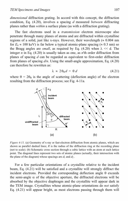
TEM Specimens and Images 107
dimensional diffraction grating. In accord with this concept, the diffractioncondition, Eq. (4.20), involves a spacing d measured between diffracting lanes rather than within a surface plane (as with a diffraction grating).p
The fast electrons used in a transmission electron microscope alsopenetrate through many planes of atoms and are diffracted within crystallineregions of a solid, just like x-rays. However, their wavelength ( 0.004 nmfor E0 100 keV) is far below a typical atomic-plane spacing ( 0.3 nm) sothe Bragg angles are small, as required by Eq. (4.20) when << d. Theinteger n in Eq. (4.20) is usually taken as one, as n'th order diffraction from planes of spacing d can be regarded as equivalent to first-order diffractionfrom planes of spacing d/n. Using the small-angle approximation, Eq. (4.20)can therefore be rewritten as:
2 B d = d (4.21)
where = 2 B is the angle of scattering (deflection angle) of the electron resulting from the diffraction process; see Fig. 4-11a.
d
R
L
d2
d1
(a) (b)
e-
diffractedbeam
undiffractedbeam
incidentbeam
Figure 4-11. (a) Geometry of x-ray or fast-electron diffraction from atomic planes, which are shown as parallel dashed lines; R is the radius of the diffraction ring at the recording plane(not to scale). (b) Schematic cross section through a cubic lattice with an atom at each latticepoint. The diagonal lines represent two sets of atomic planes (actually, their intersection withthe plane of the diagram) whose spacings are d1 and d2 .
For a few particular orientations of a crystallite relative to the incidentbeam, Eq. (4.21) will be satisfied and a crystallite will strongly diffract the incident electrons. Provided the corresponding deflection angle exceedsthe semi-angle of the objective aperture, the diffracted electrons will be absorbed by the objective diaphragm and the crystallite will appear dark in the TEM image. Crystallites whose atomic-plane orientations do not satisfy Eq. (4.21) will appear bright, as most electrons passing through them will
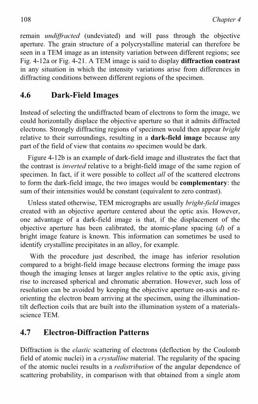
108 Chapter 4
remain undiffracted (undeviated) and will pass through the objectiveaperture. The grain structure of a polycrystalline material can therefore be seen in a TEM image as an intensity variation between different regions; see Fig. 4-12a or Fig. 4-21. A TEM image is said to display diffraction contrast
in any situation in which the intensity variations arise from differences indiffracting conditions between different regions of the specimen.
4.6 Dark-Field Images
Instead of selecting the undiffracted beam of electrons to form the image, wecould horizontally displace the objective aperture so that it admits diffractedelectrons. Strongly diffracting regions of specimen would then appear bright
relative to their surroundings, resulting in a dark-field image because any art of the field of view that contains no specimen would be dark.p
Figure 4-12b is an example of dark-field image and illustrates the fact that the contrast is inverted relative to a bright-field image of the same region of specimen. In fact, if it were possible to collect all of the scattered electronsto form the dark-field image, the two images would be complementary: theum of their intensities would be constant (equivalent to zero contrast).s
Unless stated otherwise, TEM micrographs are usually bright-field imagescreated with an objective aperture centered about the optic axis. However, one advantage of a dark-field image is that, if the displacement of the objective aperture has been calibrated, the atomic-plane spacing (d) of abright image feature is known. This information can sometimes be used to identify crystalline precipitates in an alloy, for example.
With the procedure just described, the image has inferior resolutioncompared to a bright-field image because electrons forming the image passthough the imaging lenses at larger angles relative to the optic axis, givingrise to increased spherical and chromatic aberration. However, such loss of resolution can be avoided by keeping the objective aperture on-axis and re-orienting the electron beam arriving at the specimen, using the illumination-tilt deflection coils that are built into the illumination system of a materials-science TEM.
4.7 Electron-Diffraction Patterns
Diffraction is the elastic scattering of electrons (deflection by the Coulombfield of atomic nuclei) in a crystalline material. The regularity of the spacingof the atomic nuclei results in a redistribution of the angular dependence ofscattering probability, in comparison with that obtained from a single atom
TEM Specimens and Images 109
(discussed in Section 4.3). Instead of a continuous angular distribution, as depicted in Fig. 4-5, the scattering is concentrate`d into sharp peaks (knownas Bragg peaks; see Fig. 4-12d) that occur at scattering angles that are twice
the Bragg angle B for atomic planes of a particular orientation.
Figure 4-12. (a) Bright-field TEM image of a polycrystalline thin film of bismuth, includingbend contours that appear dark. (b) Dark-field image of the same area; bend contours appear bright. (c) Ring diffraction pattern obtained from many crystallites; for recording purposes, the central (0,0,0) diffraction spot has been masked by a wire. (d) Spot diffraction pattern recorded from a single Bi crystallite, whose trigonal crystal axis was parallel to the incidentbeam. Courtesy of Marek Malac, National Institute of Nanotechnology, Canada.
This angular distribution of scattering can be displayed on the TEMscreen by weakening the intermediate lens, so that the intermediate and projector lenses magnify the small diffraction pattern initially formed at the back-focal plane of the objective lens. Figure 4-12c is typical of the pattern obtained from a polycrystalline material. It consists of concentric rings, centered on a bright central spot that represents the undiffracted electrons. Each ring corresponds to atomic planes of different orientation and different interplanar spacing d, as indicated in Fig. 4-11b.
110 Chapter 4
Close examination of the rings reveals that they consist of a large numberof spots, each arising from Bragg reflection from an individual crystallite.Equation (4.21) predicts only the radial angle ( = 2 B) that determines thedistance of a spot from the center of the diffraction pattern. The azimuthalangle of a spot is determined by the azimuthal orientation of a crystalliteabout the incident-beam direction (the optic axis). Because the grains in apolycrystalline specimen are randomly oriented, diffraction spots occur at all azimuthal angles and give the appearance of continuous rings if many grainslie within the path of the electron beam (grain size << beam diameter at the specimen).
The radius R of a given diffraction ring depends not only on thescattering angle but also on how much the TEM magnifies the initialdiffraction pattern formed at the objective back-focal plane. If there were no imaging lenses and a diffraction pattern were recorded at a distance L fromthe specimen, simple geometry (Fig. 4-11a) gives:
R = L tan (4.22)
In practice, imaging lenses are present and the relationship between R and depends on the excitation of these lenses. We can still use Eq. (4.22) to represent this relationship, however L no longer represents a real physicaldistance. Instead, L is a measure of the scale of the diffraction pattern and is known as the camera length. Its value can be changed (typically over therange 10 150 cm) by varying the excitation current of the intermediate lens.In a modern TEM, the camera length is displayed on the control panel when
iffraction mode is selected.d
Knowing L and (from the accelerating voltage V0) the wavelength , the d-spacing of each set of atomic planes that contribute to the diffractionpattern can be calculated using Eq. (4.21) and Eq. (4.22). The nearest-neighbor spacing of atoms in the specimen is, in general, not equal to d ; it depends also on the arrangement of the atoms within the unit cell (the smallest repeat unit) of the crystal. Many metals, such as copper andaluminum, have a face-centered cubic (fcc) unit cell (see Fig. 4-13), for which:
d = a / (h2 + k2 + l2)1/2 (4.23)
Here, a is the lattice parameter (dimension of the unit cell), and h, k, and lare integers (known as Miller indices) that describe the orientation of theplanes (of spacing d) relative to the x, y, and z crystal axes (which areparallel to the edges of the unit cell). From Eq. (4.23), larger Miller indices correspond to smaller d and, according to Eq. (4.21) and Eq. (4.22), to larger
B and R.
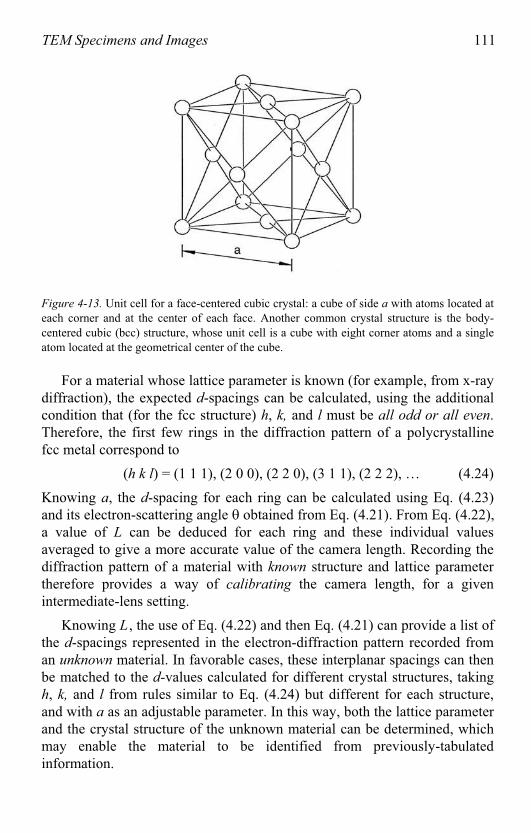
TEM Specimens and Images 111
Figure 4-13. Unit cell for a face-centered cubic crystal: a cube of side a with atoms located ateach corner and at the center of each face. Another common crystal structure is the body-centered cubic (bcc) structure, whose unit cell is a cube with eight corner atoms and a single atom located at the geometrical center of the cube.
For a material whose lattice parameter is known (for example, from x-ray diffraction), the expected d-spacings can be calculated, using the additionalcondition that (for the fcc structure) h, k, and l must be all odd or all even.Therefore, the first few rings in the diffraction pattern of a polycrystallinefcc etal correspond tom
(h k l) = (1 1 1), (2 0 0), (2 2 0), (3 1 1), (2 2 2), … (4.24)
Knowing a, the d-spacing for each ring can be calculated using Eq. (4.23) and its electron-scattering angle obtained from Eq. (4.21). From Eq. (4.22),a value of L can be deduced for each ring and these individual valuesaveraged to give a more accurate value of the camera length. Recording the diffraction pattern of a material with known structure and lattice parametertherefore provides a way of calibrating the camera length, for a given intermediate-lens setting.
Knowing L , the use of Eq. (4.22) and then Eq. (4.21) can provide a list ofthe d-spacings represented in the electron-diffraction pattern recorded from an unknown material. In favorable cases, these interplanar spacings can then be matched to the d-values calculated for different crystal structures, taking h, k, and l from rules similar to Eq. (4.24) but different for each structure,and with a as an adjustable parameter. In this way, both the lattice parameter and the crystal structure of the unknown material can be determined, whichmay enable the material to be identified from previously-tabulatedinformation.
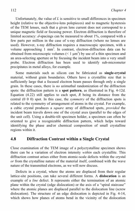
112 Chapter 4
Unfortunately, the value of L is sensitive to small differences in specimenheight (relative to the objective-lens polepieces) and to magnetic hysteresisof the TEM lenses, such that a given lens current does not correspond to a unique magnetic field or focusing power. Electron diffraction is therefore of limited accuracy: d-spacings can be measured to about 1%, compared with a few parts per million in the case of x-ray diffraction (where no lenses areused). However, x-ray diffraction requires a macroscopic specimen, with a volume approaching 1 mm3. In contrast, electron-diffraction data can be obtained from microscopic volumes (< 1 m3) by use of a thin specimen andan area-selecting aperture or by focusing the incident beam into a very smallprobe. Electron diffraction has been used to identify sub-micrometerprecipitates in metal alloys, for example.
Some materials such as silicon can be fabricated as single-crystal
material, without grain boundaries. Others have a crystallite size that is sufficiently large that a focused electron beam passes through only a singlegrain. In these cases, there is no azimuthal randomization of the diffractionspots: the diffraction pattern is a spot pattern, as illustrated in Fig. 4-12d.Equation (4.22) still applies to each spot, R being its distance from the central (0 0 0) spot. In this case, the symmetry of the diffraction spots isrelated to the symmetry of arrangement of atoms in the crystal. For example,a cubic crystal produces a square array of diffracted spots, provided the incident beam travels down one of the crystal axes (parallel to the edges of the unit cell). Using a double-tilt specimen holder, a specimen can often beoriented to give a recognizable diffraction pattern, which helps towardidentifying the phase and/or chemical composition of small crystallineregions within it.
4.8 Diffraction Contrast within a Single Crystal
Close examination of the TEM image of a polycrystalline specimen shows there can be a variation of electron intensity within each crystallite. Thisdiffraction contrast arises either from atomic-scale defects within the crystalor from the crystalline nature of the material itself, combined with the wave
ature of the transmitted electrons, as we will now discuss.n
Defects in a crystal, where the atoms are displaced from their regularlattice-site positions, can take several different forms. A dislocation is an example of a line defect. It represents either the termination of an atomicplane within the crystal (edge dislocation) or the axis of a “spiral staircase”where the atomic planes are displaced parallel to the dislocation line (screwdislocation). The structure of an edge dislocation is depicted in Fig. 4-14,which shows how planes of atoms bend in the vicinity of the dislocation
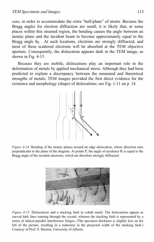
TEM Specimens and Images 113
core, in order to accommodate the extra “half-plane” of atoms. Because theBragg angles for electron diffraction are small, it is likely that, at someplaces within this strained region, the bending causes the angle between anatomic plane and the incident beam to become approximately equal to the Bragg angle B . At such locations, electrons are strongly diffracted, and most of these scattered electrons will be absorbed at the TEM objective aperture. Consequently, the dislocation appears dark in the TEM image, asshown in Fig. 4-15.
Because they are mobile, dislocations play an important role in the deformation of metals by applied mechanical stress. Although they had beenpredicted to explain a discrepancy between the measured and theoreticalstrengths of metals, TEM images provided the first direct evidence for the existence and morphology (shape) of dislocations; see Fig. 1-11 on p. 14.
PP
i
Figure 4-14. Bending of the atomic planes around an edge dislocation, whose direction runs perpendicular to the plane of the diagram. At points P, the angle of incidence i is equal to theBragg angle of the incident electrons, which are therefore strongly diffracted.
Figure 4-15. Dislocations and a stacking fault in cobalt metal. The dislocations appear ascurved dark lines running through the crystal, whereas the stacking fault is represented by aseries of almost-parallel interference fringes. (The specimen thickness is slightly less on the left of the picture, resulting in a reduction in the projected width of the stacking fault.)Courtesy of Prof. S. Sheinin, University of Alberta.
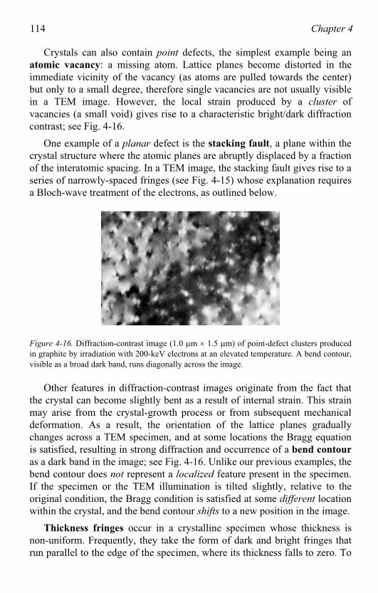
114 Chapter 4
Crystals can also contain point defects, the simplest example being an atomic vacancy: a missing atom. Lattice planes become distorted in theimmediate vicinity of the vacancy (as atoms are pulled towards the center) but only to a small degree, therefore single vacancies are not usually visible in a TEM image. However, the local strain produced by a cluster of vacancies (a small void) gives rise to a characteristic bright/dark diffractioncontrast; see Fig. 4-16.
One example of a planar defect is the stacking fault, a plane within the crystal structure where the atomic planes are abruptly displaced by a fraction of the interatomic spacing. In a TEM image, the stacking fault gives rise to aseries of narrowly-spaced fringes (see Fig. 4-15) whose explanation requires a Bloch-wave treatment of the electrons, as outlined below.
Figure 4-16. Diffraction-contrast image (1.0 m 1.5 m) of point-defect clusters produced in graphite by irradiation with 200-keV electrons at an elevated temperature. A bend contour,visible as a broad dark band, runs diagonally across the image.
Other features in diffraction-contrast images originate from the fact that the crystal can become slightly bent as a result of internal strain. This strain may arise from the crystal-growth process or from subsequent mechanicaldeformation. As a result, the orientation of the lattice planes graduallychanges across a TEM specimen, and at some locations the Bragg equation is satisfied, resulting in strong diffraction and occurrence of a bend contour
as a dark band in the image; see Fig. 4-16. Unlike our previous examples, thebend contour does not represent a localized feature present in the specimen.If the specimen or the TEM illumination is tilted slightly, relative to theoriginal condition, the Bragg condition is satisfied at some different locationwithin the crystal, and the bend contour shifts to a new position in the image.
Thickness fringes occur in a crystalline specimen whose thickness is non-uniform. Frequently, they take the form of dark and bright fringes that run parallel to the edge of the specimen, where its thickness falls to zero. To
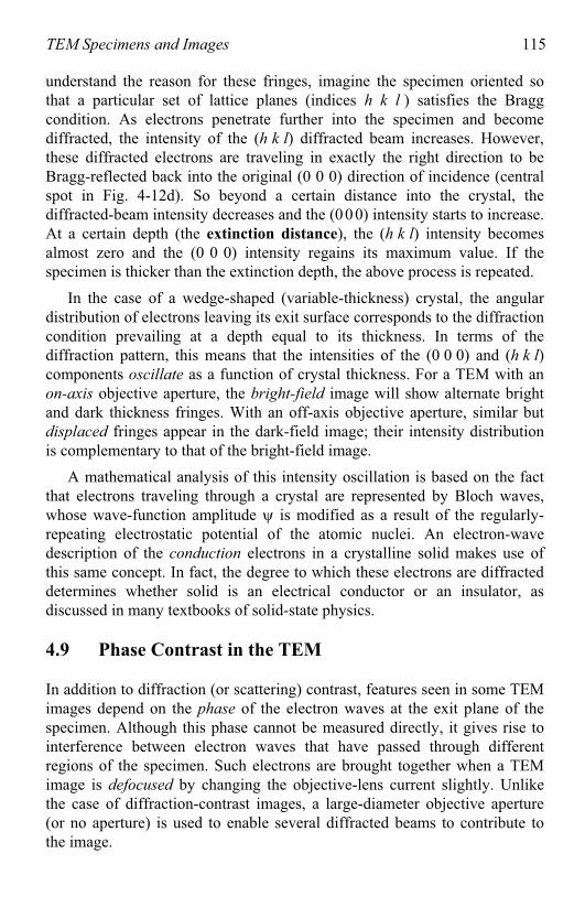
TEM Specimens and Images 115
understand the reason for these fringes, imagine the specimen oriented so that a particular set of lattice planes (indices h k l ) satisfies the Bragg condition. As electrons penetrate further into the specimen and become diffracted, the intensity of the (h k l) diffracted beam increases. However,these diffracted electrons are traveling in exactly the right direction to beBragg-reflected back into the original (0 0 0) direction of incidence (central spot in Fig. 4-12d). So beyond a certain distance into the crystal, the diffracted-beam intensity decreases and the (000) intensity starts to increase.At a certain depth (the extinction distance), the (h k l) intensity becomes almost zero and the (0 0 0) intensity regains its maximum value. If the specimen is thicker than the extinction depth, the above process is repeated.
In the case of a wedge-shaped (variable-thickness) crystal, the angulardistribution of electrons leaving its exit surface corresponds to the diffractioncondition prevailing at a depth equal to its thickness. In terms of the diffraction pattern, this means that the intensities of the (0 0 0) and (h k l)components oscillate as a function of crystal thickness. For a TEM with anon-axis objective aperture, the bright-field image will show alternate bright and dark thickness fringes. With an off-axis objective aperture, similar butdisplaced fringes appear in the dark-field image; their intensity distributionis complementary to that of the bright-field image.
A mathematical analysis of this intensity oscillation is based on the factthat electrons traveling through a crystal are represented by Bloch waves, whose wave-function amplitude is modified as a result of the regularly-repeating electrostatic potential of the atomic nuclei. An electron-wave description of the conduction electrons in a crystalline solid makes use of this same concept. In fact, the degree to which these electrons are diffracteddetermines whether solid is an electrical conductor or an insulator, as discussed in many textbooks of solid-state physics.
4.9 Phase Contrast in the TEM
In addition to diffraction (or scattering) contrast, features seen in some TEM images depend on the phase of the electron waves at the exit plane of the specimen. Although this phase cannot be measured directly, it gives rise to interference between electron waves that have passed through differentregions of the specimen. Such electrons are brought together when a TEM image is defocused by changing the objective-lens current slightly. Unlikethe case of diffraction-contrast images, a large-diameter objective aperture (or no aperture) is used to enable several diffracted beams to contribute to the image.
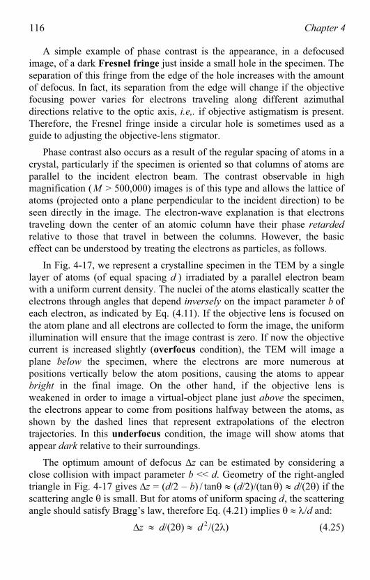
116 Chapter 4
A simple example of phase contrast is the appearance, in a defocused image, of a dark Fresnel fringe just inside a small hole in the specimen. The separation of this fringe from the edge of the hole increases with the amountof defocus. In fact, its separation from the edge will change if the objective focusing power varies for electrons traveling along different azimuthaldirections relative to the optic axis, i.e,. if objective astigmatism is present.Therefore, the Fresnel fringe inside a circular hole is sometimes used as aguide to adjusting the objective-lens stigmator.
Phase contrast also occurs as a result of the regular spacing of atoms in a crystal, particularly if the specimen is oriented so that columns of atoms areparallel to the incident electron beam. The contrast observable in highmagnification (M > 500,000) images is of this type and allows the lattice of atoms (projected onto a plane perpendicular to the incident direction) to beseen directly in the image. The electron-wave explanation is that electronstraveling down the center of an atomic column have their phase retarded
relative to those that travel in between the columns. However, the basic effect can be understood by treating the electrons as particles, as follows.
In Fig. 4-17, we represent a crystalline specimen in the TEM by a singlelayer of atoms (of equal spacing d ) irradiated by a parallel electron beamwith a uniform current density. The nuclei of the atoms elastically scatter the electrons through angles that depend inversely on the impact parameter b ofeach electron, as indicated by Eq. (4.11). If the objective lens is focused on the atom plane and all electrons are collected to form the image, the uniform illumination will ensure that the image contrast is zero. If now the objective current is increased slightly (overfocus condition), the TEM will image a plane below the specimen, where the electrons are more numerous atpositions vertically below the atom positions, causing the atoms to appear bright in the final image. On the other hand, if the objective lens is weakened in order to image a virtual-object plane just above the specimen,the electrons appear to come from positions halfway between the atoms, asshown by the dashed lines that represent extrapolations of the electron trajectories. In this underfocus condition, the image will show atoms that appear dark relative to their surroundings.
The optimum amount of defocus z can be estimated by considering aclose collision with impact parameter b << d. Geometry of the right-angledtriangle in Fig. 4-17 gives z = (d/2 – b) / tan (d/2)/(tan ) d/(2 ) if the scattering angle is small. But for atoms of uniform spacing d, the scatteringangle should satisfy Bragg’s law, therefore Eq. (4.21) implies /d and:
z d/(2 ) d 2 /(2 ) (4.25)
TEM Specimens and Images 117
overfocus atoms bright
underfocus atoms dark
no contrastatom plane
z > 0)
z
d/2
b
z < 0)
d
Figure 4-17. Equally spaced atomic nuclei that are elastically scattering the electrons within a broad incident beam, which provides a continuous range of impact parameter b. The electroncurrent density appears non-uniform at planes above and below the atom plane.
For E0 = 200 keV, = 2.5 pm and taking d = 0.3 nm, we obtain z 18 nm,therefore the amount of defocus required for atomic resolution is small.Wave-optical theory gives expression identical to Eq. (4.25), for an objectivelens with no spherical aberration. In practice, spherical aberration is important and should be included in the theory (Reimer, 1998). Clearly, theinterpretation of phase-contrast images requires that the spherical-aberration coefficient of the objective and the amount of defocus are known. In fact, a detailed interpretation of atomic-resolution lattice images often requires recording a through-focus series of images with positive and negative z.
Figure 4-18. (a) Lattice image of ZnS crystals embedded within a sapphire matrix. (b) Detailof a grain boundary between a PbS crystal and its sapphire matrix. Courtesy of Al Meldrum, University of Alberta.
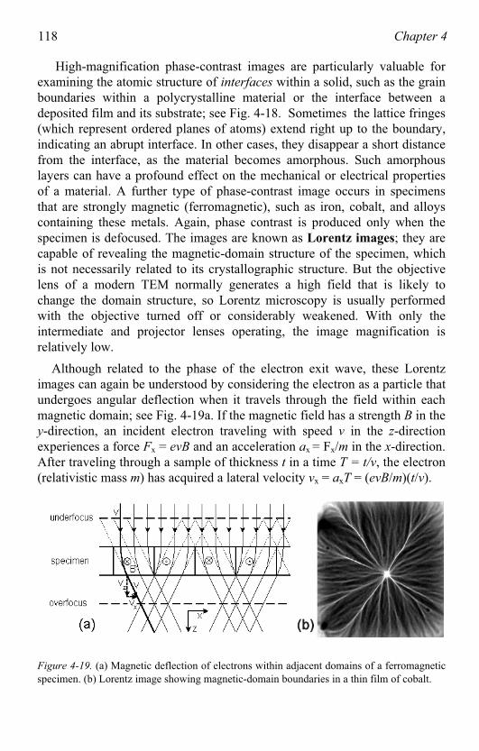
118 Chapter 4
High-magnification phase-contrast images are particularly valuable for examining the atomic structure of interfaces within a solid, such as the grain boundaries within a polycrystalline material or the interface between adeposited film and its substrate; see Fig. 4-18. Sometimes the lattice fringes (which represent ordered planes of atoms) extend right up to the boundary,indicating an abrupt interface. In other cases, they disappear a short distancefrom the interface, as the material becomes amorphous. Such amorphouslayers can have a profound effect on the mechanical or electrical propertiesof a material. A further type of phase-contrast image occurs in specimensthat are strongly magnetic (ferromagnetic), such as iron, cobalt, and alloyscontaining these metals. Again, phase contrast is produced only when the specimen is defocused. The images are known as Lorentz images; they are capable of revealing the magnetic-domain structure of the specimen, which is not necessarily related to its crystallographic structure. But the objective lens of a modern TEM normally generates a high field that is likely tochange the domain structure, so Lorentz microscopy is usually performedwith the objective turned off or considerably weakened. With only theintermediate and projector lenses operating, the image magnification is relatively low.
Although related to the phase of the electron exit wave, these Lorentzimages can again be understood by considering the electron as a particle that undergoes angular deflection when it travels through the field within eachmagnetic domain; see Fig. 4-19a. If the magnetic field has a strength B in the y-direction, an incident electron traveling with speed v in the z-directionexperiences a force Fx = evB and an acceleration ax = Fx/m in the x-direction.After traveling through a sample of thickness t in a time T = t/v, the electron(relativistic mass m) has acquired a lateral velocity vx = axT = (evB/m)(t/v).
Figure 4-19. (a) Magnetic deflection of electrons within adjacent domains of a ferromagneticspecimen. (b) Lorentz image showing magnetic-domain boundaries in a thin film of cobalt.
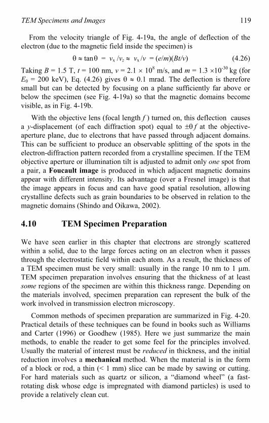
TEM Specimens and Images 119
From the velocity triangle of Fig. 4-19a, the angle of deflection of the electron (due to the magnetic field inside the specimen) is
tan = vx /vz vx /v = (e/m)(Bt/v) (4.26)
Taking B = 1.5 T, t = 100 nm, v = 2.1 108 m/s, and m = 1.3 10-30 kg (forE0 = 200 keV), Eq. (4.26) gives 0.1 mrad. The deflection is therefore small but can be detected by focusing on a plane sufficiently far above or below the specimen (see Fig. 4-19a) so that the magnetic domains becomevisible, as in Fig. 4-19b.
With the objective lens (focal length f ) turned on, this deflection causes a y-displacement (of each diffraction spot) equal to f at the objective-aperture plane, due to electrons that have passed through adjacent domains.This can be sufficient to produce an observable splitting of the spots in theelectron-diffraction pattern recorded from a crystalline specimen. If the TEM objective aperture or illumination tilt is adjusted to admit only one spot froma pair, a Foucault image is produced in which adjacent magnetic domainsappear with different intensity. Its advantage (over a Fresnel image) is thatthe image appears in focus and can have good spatial resolution, allowing crystalline defects such as grain boundaries to be observed in relation to themagnetic domains (Shindo and Oikawa, 2002).
4.10 TEM Specimen Preparation
We have seen earlier in this chapter that electrons are strongly scatteredwithin a solid, due to the large forces acting on an electron when it passes through the electrostatic field within each atom. As a result, the thickness ofa TEM specimen must be very small: usually in the range 10 nm to 1 m.TEM specimen preparation involves ensuring that the thickness of at leastsome regions of the specimen are within this thickness range. Depending on the materials involved, specimen preparation can represent the bulk of the
ork involved in transmission electron microscopy.w
Common methods of specimen preparation are summarized in Fig. 4-20.Practical details of these techniques can be found in books such as Williamsand Carter (1996) or Goodhew (1985). Here we just summarize the mainmethods, to enable the reader to get some feel for the principles involved.Usually the material of interest must be reduced in thickness, and the initial reduction involves a mechanical method. When the material is in the form of a block or rod, a thin (< 1 mm) slice can be made by sawing or cutting.For hard materials such as quartz or silicon, a “diamond wheel” (a fast-rotating disk whose edge is impregnated with diamond particles) is used toprovide a relatively clean cut.
120 Chapter 4
At this stage it is convenient to cut a 3-mm-diameter disk out of the slice. For reasonably soft metals (e.g., aluminum, copper), a mechanical punch may be used. For harder materials, an ultrasonic drill is necessary; itconsists of a thin-walled tube (internal diameter = 3 mm) attached to a piezoelectric crystal that changes slightly in length when a voltage is appliedbetween electrodes on its surfaces; see Fig. 4-20a. The tube is lowered onto the slice, which has been bonded to a solid support using by heat-setting wax and its top surface pre-coated with a silicon-carbide slurry (SiC powder mixed with water). Upon applying a high-frequency ac voltage, the tubeoscillates vertically thousands of times per second, driving SiC particles against the sample and cutting an annular groove in the slice. When the slice has been cut through completely, the wax is melted and the 3-mm disk is retrieved with tweezers.
The disk is then thinned further by polishing with abrasive paper (coated with diamond or silicon carbide particles) or by using a dimple grinder. Inthe latter case (Fig. 4-20b), a metal wheel rotates rapidly against the surface (covered with a SiC slurry or diamond paste) while the specimen disk is rotated slowly about a vertical axis. The result is a dimpled specimen whosethickness is 10 50 m at the center but greater (100 400 m) at the outside, which provides the mechanical strength needed for easy handling.
In the case of biological tissue, a common procedure is to use anultramicrotome to directly cut slices 100 nm or more in thickness. The tissue block is lowered onto a glass or diamond knife that cleaves the material apart (Fig. 4-20c). The ultramicrotome can also be used to cut thin slices of the softer metals, such as aluminum.
Some inorganic materials (e.g., graphite, mica) have a layered structure,with weak forces between sheets of atoms, and are readily cleaved apart by inserting the tip of a knife blade. Repeated cleavage, achieved by attachingadhesive tape to each surface and pulling apart, can reduce the thickness to below 1 m. After dissolving the adhesive, thin flakes are mounted on 3-mmTEM grids. Other materials, such as silicon, can sometimes be persuaded tocleave along a plane cut at a small angle relative to a natural (crystallographic) cleavage plane. If so, a second cleavage along acrystallographic plane results in a wedge of material whose thin end istransparent to electrons. Mechanical cleavage is also involved when a material is ground into a fine powder, using a pestle and mortar, for example(Fig. 4-20d). The result is a fine powder, whose particles or flakes may be thin enough for electron transmission. They are dispersed onto a 3-mm TEM grid covered with a thin carbon film (sometimes containing small holes sothat some particles are supported only at their edges).
TEM Specimens and Images 121
~
+
+
-
+
-
+ +
(a) (b)
(c) (d)
(e) (f)
(g) (h)
Ar
gas
vacuum
Ar+ film
specimen
specimen
tissue
blockwater
trough
pestle
mortar
SiC
slurry
piezo
crystal
wax
powder
specimen
jetelectrolysis
solution
specimenwax
grinding
wheel
microtome
arm
substrate
boat
current
vacuum
chamber
cathode
Figure 4-20. Procedures used in making TEM specimens: (a) disk cutting by ultrasonic drill, (b) dimple grinding, (c) ultramicrotomy, (d) grinding to a powder, (e) chemical jet thinning,(f) electrochemical thinning, (g) ion-beam thinning, and (h) vacuum deposition of a thin film.Methods (a) (d) are mechanical, (e) and (f) are chemical, (g) and (h) are vacuum techniques.
122 Chapter 4
All of the above methods involve the application of a mechanical force to achieve thinning. Unfortunately, for all but the most well-behaved materials(e.g., biological tissue, layer materials, silicon), the specimen becomes extremely fragile and cannot be mechanically thinned below about 1 m. Inaddition, the mechanical forces involved may leave a damaged surface layer,containing a high density of defects such as dislocations. This damage is undesirable if the TEM is being used to study the original defect structure of the specimen. Therefore, some non-mechanical method is commonly usedfor the final thinning.
One such method is chemical thinning, in which a chemical solutiondissolves the original surface and reduces the specimen thickness to a value suitable for TEM imaging. In the simplest case, a thin piece of material isfloated onto the surface of a chemical solution that attacks its lower surface;the sample is retrieved (e.g, by picking up by a TEM grid held in tweezers) before it dissolves completely. More commonly, a jet of chemical solution isdirected at one or both surfaces of a thin disk. As soon as a small hole formsin the center (detected by the transmission of a light beam), the polishing solution is replaced by rinse water. If the procedure is successful, regions of the specimen surrounding the hole are thin enough for TEM examination.
Alternatively, electrochemical thinning is carried out with a directcurrent flowing between the specimen (at a negative potential) and a positive electrode, immersed in a chemical solution. In the original window-framemethod (Fig. 4-20f), the specimen is in the form of a thin sheet (1 cm or more in height and width) whose four edges are previously painted withprotective lacquer to prevent erosion at the edge. When partially immersedin the electrolytic solution, thinning is most rapid at the liquid/air interface,which perforates first. Small pieces of foil are cut adjacent to the perforatededge and mounted on a TEM grid. Nowadays, electrochemical thinning is usually done using the jet-thinning geometry (Fig. 4-20e), by applying a dcvoltage between the specimen and jet electrodes. Recipes for the solutions used in chemical and electrochemical thinning are given in Goodhew (1985).When thinning metals, glycerin is sometimes added to the solution to makethe liquid more viscous, helping to give the thinned specimen a polished
(microscopically smooth) surface.
Increasingly, ion-beam thinning is used for the final thinning stage, particularly of materials that are chemically inert. Following mechanicalthinning (if necessary), a 3mm-diameter thin disk of the material is placed in a vacuum system, where it is bombarded by argon ions produced by a gasdischarge within an ion gun. These ions transfer energy to surface atoms andremove the material by the process of sputtering; see Fig. 4-20g. A focused
ion beam (FIB) machine uses a beam of gallium ions to cut thin slices, often
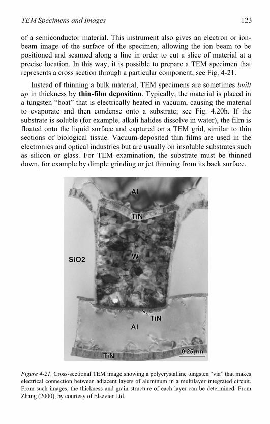
TEM Specimens and Images 123
of a semiconductor material. This instrument also gives an electron or ion-beam image of the surface of the specimen, allowing the ion beam to bepositioned and scanned along a line in order to cut a slice of material at a precise location. In this way, it is possible to prepare a TEM specimen that represents a cross section through a particular component; see Fig. 4-21.
Instead of thinning a bulk material, TEM specimens are sometimes built
up in thickness by thin-film deposition. Typically, the material is placed ina tungsten “boat” that is electrically heated in vacuum, causing the materialto evaporate and then condense onto a substrate; see Fig. 4.20h. If the substrate is soluble (for example, alkali halides dissolve in water), the film isfloated onto the liquid surface and captured on a TEM grid, similar to thin sections of biological tissue. Vacuum-deposited thin films are used in theelectronics and optical industries but are usually on insoluble substrates such as silicon or glass. For TEM examination, the substrate must be thinned down, for example by dimple grinding or jet thinning from its back surface.
Figure 4-21. Cross-sectional TEM image showing a polycrystalline tungsten “via” that makeselectrical connection between adjacent layers of aluminum in a multilayer integrated circuit.From such images, the thickness and grain structure of each layer can be determined. FromZhang (2000), by courtesy of Elsevier Ltd.
124 Chapter 4
The procedures outlined in Fig. 4-20 yield plan-view images, in which the sample is viewed perpendicular to its original surface. For somepurposes, a cross-sectional image is needed, for example to show the growth mechanism of a film. The required specimen is made by using a diamondwheel to cut the film (on its substrate) into several thin strips, which are then turned through 90 degrees about their long axis and glued together by epoxy cement. Dimple grinding followed by ion milling then produces a specimenthat is thin at the center, resulting in a TEM image of the substrate and film seen in cross section.
Cross-sectional specimens are invaluable for analyzing problems thatarise in the manufacture of integrated circuits on a silicon chip. As device sizes shrink, it becomes necessary to make use of the high spatial resolution of the TEM for this kind of failure analysis. The problem of producing a cross section containing a specific component is solved by using a FIBmachine, in which Ga+ ions are focused (by electrostatic lenses) into a beamas small as 10 nm in diameter. The machine produces a scanned image of thesurface of the chip, allowing the ion beam to be precisely positioned and then scanned in a line in order to cut into the silicon on either side of thecomponent. This leaves a slice only 100 nm in thickness, which is then lifted out and viewed in cross section in the TEM, as in Fig. 4-21.
Chapter 5
THE SCANNING ELECTRON MICROSCOPE
As we discussed in Chapter 1, the scanning electron microscope (SEM) wasinvented soon after the TEM but took longer to be developed into a practical tool for scientific research. As happened with the TEM, the spatial resolution of the instrument improved after magnetic lenses were substituted for electrostatic ones and after a stigmator was added to the lens column. Today,scanning electron microscopes outnumber transmission electron microscopesand are used in many fields, including medical and materials research, theemiconductor industry, and forensic-science laboratories.s
Figure 1-15 (page 19) shows one example of a commercial high-resolution SEM. Although smaller (and generally less expensive) than a TEM, the SEM incorporates an electron-optical column that operatesaccording to the principles already discussed in Chapter 2 and Chapter 3. Accordingly, our description will be shorter than for the TEM, as we canmake use of many of the concepts introduced in these earlier chapters.
5.1 Operating Principle of the SEM
The electron source used in the SEM can be a tungsten filament, or else aLaB6 or Schottky emitter, or a tungsten field-emission tip. Because the maximum accelerating voltage (typically 30 kV) is lower than for a TEM, the electron gun is smaller, requiring less insulation. Axially-symmetricmagnetic lenses are used but they are also smaller than those employed in the TEM; for electrons of lower kinetic energy, the polepieces need not generate such a strong magnetic field. There are also fewer lenses; imageformation uses the scanning principle that was outlined in Chapter 1, and as a result imaging lenses are not required.
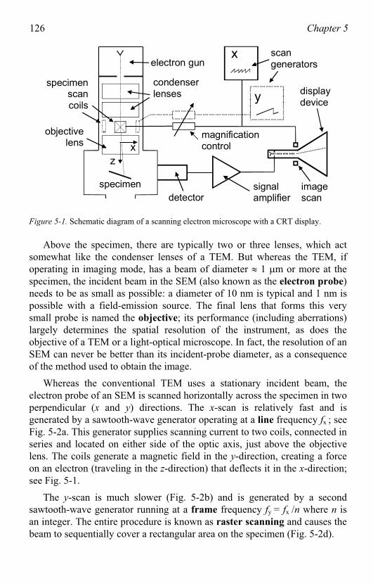
126 Chapter 5
electron gun
condenserlenses
specimenscancoils
specimen
detectorsignalamplifier
displaydevice
magnificationcontrol
imagescan
scangenerators
objectivelens
x
y
x
z
Figure 5-1. Schematic diagram of a scanning electron microscope with a CRT display.
Above the specimen, there are typically two or three lenses, which act somewhat like the condenser lenses of a TEM. But whereas the TEM, if operating in imaging mode, has a beam of diameter 1 m or more at the specimen, the incident beam in the SEM (also known as the electron probe)needs to be as small as possible: a diameter of 10 nm is typical and 1 nm is possible with a field-emission source. The final lens that forms this very small probe is named the objective; its performance (including aberrations)largely determines the spatial resolution of the instrument, as does theobjective of a TEM or a light-optical microscope. In fact, the resolution of an SEM can never be better than its incident-probe diameter, as a consequence of the method used to obtain the image.
Whereas the conventional TEM uses a stationary incident beam, theelectron probe of an SEM is scanned horizontally across the specimen in two perpendicular (x and y) directions. The x-scan is relatively fast and is generated by a sawtooth-wave generator operating at a line frequency fx ; seeFig. 5-2a. This generator supplies scanning current to two coils, connected inseries and located on either side of the optic axis, just above the objective lens. The coils generate a magnetic field in the y-direction, creating a forceon an electron (traveling in the z-direction) that deflects it in the x-direction;see Fig. 5-1.
The y-scan is much slower (Fig. 5-2b) and is generated by a secondsawtooth-wave generator running at a frame frequency fy = fx /n where n is an integer. The entire procedure is known as raster scanning and causes thebeam to sequentially cover a rectangular area on the specimen (Fig. 5-2d).
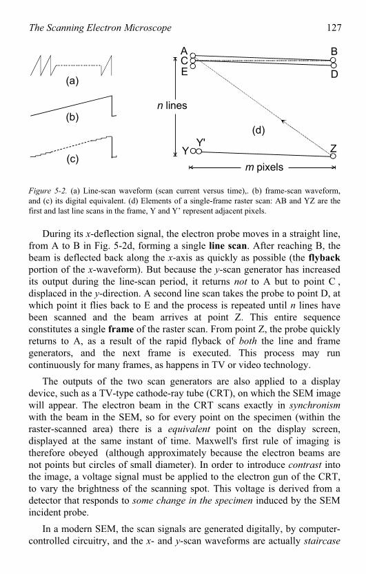
The Scanning Electron Microscope 127
m pixels
(a)
(b)
(c)
(d)
n lines
ECA
D
B
Y'Y Z
Figure 5-2. (a) Line-scan waveform (scan current versus time),. (b) frame-scan waveform,and (c) its digital equivalent. (d) Elements of a single-frame raster scan: AB and YZ are thefirst and last line scans in the frame, Y and Y’ represent adjacent pixels.
During its x-deflection signal, the electron probe moves in a straight line, from A to B in Fig. 5-2d, forming a single line scan. After reaching B, thebeam is deflected back along the x-axis as quickly as possible (the flyback
portion of the x-waveform). But because the y-scan generator has increasedits output during the line-scan period, it returns not to A but to point C ,displaced in the y-direction. A second line scan takes the probe to point D, atwhich point it flies back to E and the process is repeated until n lines havebeen scanned and the beam arrives at point Z. This entire sequence constitutes a single frame of the raster scan. From point Z, the probe quickly returns to A, as a result of the rapid flyback of both the line and framegenerators, and the next frame is executed. This process may run continuously for many frames, as happens in TV or video technology.
The outputs of the two scan generators are also applied to a displaydevice, such as a TV-type cathode-ray tube (CRT), on which the SEM imagewill appear. The electron beam in the CRT scans exactly in synchronism
with the beam in the SEM, so for every point on the specimen (within theraster-scanned area) there is a equivalent point on the display screen, displayed at the same instant of time. Maxwell's first rule of imaging is therefore obeyed (although approximately because the electron beams arenot points but circles of small diameter). In order to introduce contrast intothe image, a voltage signal must be applied to the electron gun of the CRT, to vary the brightness of the scanning spot. This voltage is derived from adetector that responds to some change in the specimen induced by the SEMincident probe.
In a modern SEM, the scan signals are generated digitally, by computer-controlled circuitry, and the x- and y-scan waveforms are actually staircase
128 Chapter 5
functions with m and n levels respectively; see Fig. 5-2c. This proceduredivides the image into a total of mn picture elements (pixels) and the SEMprobe remains stationary for a certain dwell time before jumping to the nextpixel. One advantage of digital scanning is that the SEM computer “knows” the (x, y) address of each pixel and can record the appropriate image-intensity value (also as a digitized number) in the corresponding computer-memory location. A digital image, in the form of position and intensityinformation, can therefore be stored in computer memory, on a magnetic or optical disk, or transmitted over data lines such as the Internet.
Also, the modern SEM uses a flat-panel display screen in which there isno internal electron beam. Instead, computer-generated voltages are used to sequentially define the x- and y-coordinates of a screen pixel and the SEM detector signal is applied electronically to that pixel, to change its brightness. In other respects, the raster-scanning principle is the same as for a CRT display.
Image magnification in the SEM is achieved by making the x- and y-scandistances on the specimen a small fraction of the size of the displayed image,as by definition the magnification factor M is given by:
M = (scan distance in the image) /(scan distance on the specimen) (5.1)
It is convenient to keep the image a fixed size, just filling the display screen, so increasing the magnification involves reducing the x- and y-scan currents, each in the same proportion (to avoid image distortion). Consequently, theSEM is actually working hardest (in terms of current drawn from the scangenerator) when operated at low magnification.
The scanning is sometimes done at video rate (about 60 frames/second)to generate a rapidly-refreshed image that is useful for focusing the specimenor for viewing it at low magnification. At higher magnification, or when making a permanent record of an image, slow scanning (several seconds per frame) is preferred; the additional recording time results in a higher-quality image containing less electronic noise.
The signal that modulates (alters) the image brightness can be derived from any property of the specimen that changes in response to electronbombardment. Most commonly, the emission of secondary electrons
(atomic electrons ejected from the specimen as a result of inelastic scattering) is used. However, a signal derived from backscattered electrons
(incident electrons elastically scattered through more than 90 degrees) is alsouseful. In order to understand these (and other) possibilities, we need to
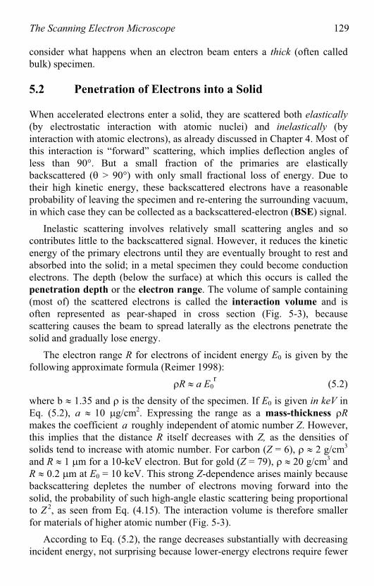
The Scanning Electron Microscope 129
consider what happens when an electron beam enters a thick (often calledbulk) specimen.
5.2 Penetration of Electrons into a Solid
When accelerated electrons enter a solid, they are scattered both elastically
(by electrostatic interaction with atomic nuclei) and inelastically (by interaction with atomic electrons), as already discussed in Chapter 4. Most of this interaction is “forward” scattering, which implies deflection angles of less than 90 . But a small fraction of the primaries are elasticallybackscattered ( > 90 ) with only small fractional loss of energy. Due to their high kinetic energy, these backscattered electrons have a reasonableprobability of leaving the specimen and re-entering the surrounding vacuum, n which case they can be collected as a backscattered-electron (BSE) signal. i
Inelastic scattering involves relatively small scattering angles and so contributes little to the backscattered signal. However, it reduces the kinetic energy of the primary electrons until they are eventually brought to rest and absorbed into the solid; in a metal specimen they could become conductionelectrons. The depth (below the surface) at which this occurs is called the penetration depth or the electron range. The volume of sample containing(most of) the scattered electrons is called the interaction volume and isoften represented as pear-shaped in cross section (Fig. 5-3), becausescattering causes the beam to spread laterally as the electrons penetrate thesolid and gradually lose energy.
The electron range R for electrons of incident energy E0 is given by thefollowing approximate formula (Reimer 1998):
R a E0r
(5.2)
where b 1.35 and is the density of the specimen. If E0 is given in keV in Eq. (5.2), a 10 g/cm2. Expressing the range as a mass-thickness R
makes the coefficient a roughly independent of atomic number Z. However, this implies that the distance R itself decreases with Z, as the densities of solids tend to increase with atomic number. For carbon (Z = 6), 2 g/cm3
and R 1 m for a 10-keV electron. But for gold (Z = 79), 20 g/cm3 and R 0.2 m at E0 = 10 keV. This strong Z-dependence arises mainly because backscattering depletes the number of electrons moving forward into thesolid, the probability of such high-angle elastic scattering being proportionalto Z 2, as seen from Eq. (4.15). The interaction volume is therefore smallerfor materials of higher atomic number (Fig. 5-3).
According to Eq. (5.2), the range decreases substantially with decreasingincident energy, not surprising because lower-energy electrons require fewer
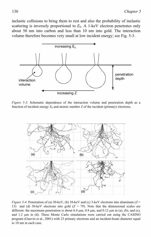
130 Chapter 5
inelastic collisions to bring them to rest and also the probability of inelastic scattering is inversely proportional to E0. A 1-keV electron penetrates onlyabout 50 nm into carbon and less than 10 nm into gold. The interactionvolume therefore becomes very small at low incident energy; see Fig. 5-3.
increasing E0
increasing Z
penetrationdepthinteraction
volume
Figure 5-3. Schematic dependence of the interaction volume and penetration depth as a function of incident energy E0 and atomic number Z of the incident (primary) electrons.
Figure 5-4. Penetration of (a) 30-keV, (b) 10-keV and (c) 3-keV electrons into aluminum (Z = 13) and (d) 30-keV electrons into gold (Z = 79). Note that the dimensional scales aredifferent: the maximum penetration is about 6.4 m, 0.8 m, and 0.12 m in (a), (b), and (c), and 1.2 m in (d). These Monte Carlo simulations were carried out using the CASINO program (Gauvin et al., 2001) with 25 primary electrons and an incident-beam diameter equalto 10 nm in each case.
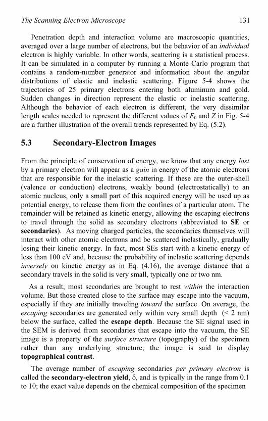
The Scanning Electron Microscope 131
Penetration depth and interaction volume are macroscopic quantities,averaged over a large number of electrons, but the behavior of an individual
electron is highly variable. In other words, scattering is a statistical process. It can be simulated in a computer by running a Monte Carlo program that contains a random-number generator and information about the angulardistributions of elastic and inelastic scattering. Figure 5-4 shows the trajectories of 25 primary electrons entering both aluminum and gold.Sudden changes in direction represent the elastic or inelastic scattering.Although the behavior of each electron is different, the very dissimilarlength scales needed to represent the different values of E0 and Z in Fig. 5-4are a further illustration of the overall trends represented by Eq. (5.2).
5.3 Secondary-Electron Images
From the principle of conservation of energy, we know that any energy lost
by a primary electron will appear as a gain in energy of the atomic electronsthat are responsible for the inelastic scattering. If these are the outer-shell(valence or conduction) electrons, weakly bound (electrostatically) to anatomic nucleus, only a small part of this acquired energy will be used up as potential energy, to release them from the confines of a particular atom. The remainder will be retained as kinetic energy, allowing the escaping electronsto travel through the solid as secondary electrons (abbreviated to SE or secondaries). As moving charged particles, the secondaries themselves willinteract with other atomic electrons and be scattered inelastically, graduallylosing their kinetic energy. In fact, most SEs start with a kinetic energy of less than 100 eV and, because the probability of inelastic scattering dependsinversely on kinetic energy as in Eq. (4.16), the average distance that a econdary travels in the solid is very small, typically one or two nm.s
As a result, most secondaries are brought to rest within the interactionvolume. But those created close to the surface may escape into the vacuum,especially if they are initially traveling toward the surface. On average, the escaping secondaries are generated only within very small depth (< 2 nm)below the surface, called the escape depth. Because the SE signal used in the SEM is derived from secondaries that escape into the vacuum, the SE image is a property of the surface structure (topography) of the specimenrather than any underlying structure; the image is said to displayopographical contrast.t
The average number of escaping secondaries per primary electron is called the secondary-electron yield, , and is typically in the range from 0.1 to 10; the exact value depends on the chemical composition of the specimen
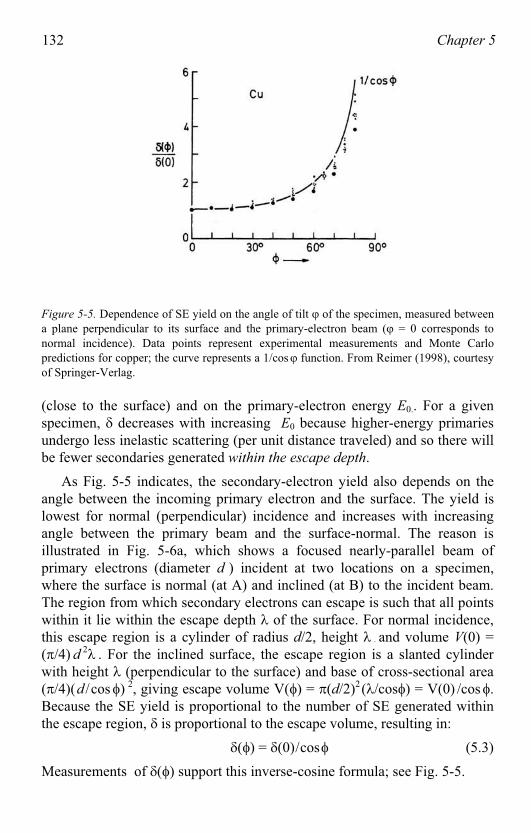
132 Chapter 5
Figure 5-5. Dependence of SE yield on the angle of tilt of the specimen, measured betweena plane perpendicular to its surface and the primary-electron beam ( = 0 corresponds tonormal incidence). Data points represent experimental measurements and Monte Carlopredictions for copper; the curve represents a 1/cos function. From Reimer (1998), courtesyof Springer-Verlag.
(close to the surface) and on the primary-electron energy E0.. For a givenspecimen, decreases with increasing E0 because higher-energy primariesundergo less inelastic scattering (per unit distance traveled) and so there will be fewer secondaries generated within the escape depth.
As Fig. 5-5 indicates, the secondary-electron yield also depends on the angle between the incoming primary electron and the surface. The yield islowest for normal (perpendicular) incidence and increases with increasingangle between the primary beam and the surface-normal. The reason isillustrated in Fig. 5-6a, which shows a focused nearly-parallel beam of primary electrons (diameter d ) incident at two locations on a specimen, where the surface is normal (at A) and inclined (at B) to the incident beam.The region from which secondary electrons can escape is such that all points within it lie within the escape depth of the surface. For normal incidence,this escape region is a cylinder of radius d/2, height , and volume V(0) = ( /4) d 2 . For the inclined surface, the escape region is a slanted cylinderwith height (perpendicular to the surface) and base of cross-sectional area( /4)(d /cos ) 2, giving escape volume V( ) = (d/2)2( /cos ) = V(0) /cos .Because the SE yield is proportional to the number of SE generated within the escape region, is proportional to the escape volume, resulting in:
( ) = (0)/cos (5.3)
Measurements of ( ) support this inverse-cosine formula; see Fig. 5-5.
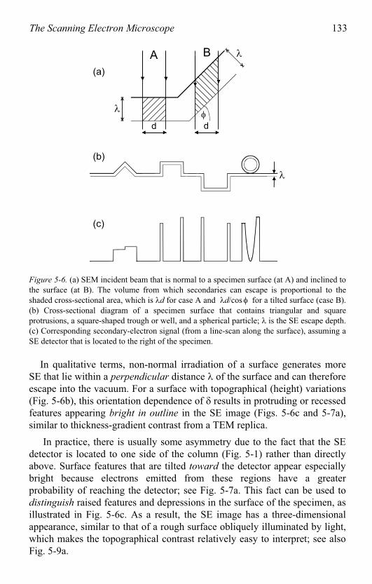
The Scanning Electron Microscope 133
(a)
(b)
(c)
A B
d d
Figure 5-6. (a) SEM incident beam that is normal to a specimen surface (at A) and inclined tothe surface (at B). The volume from which secondaries can escape is proportional to theshaded cross-sectional area, which is d for case A and d/cos for a tilted surface (case B).(b) Cross-sectional diagram of a specimen surface that contains triangular and squareprotrusions, a square-shaped trough or well, and a spherical particle; is the SE escape depth.(c) Corresponding secondary-electron signal (from a line-scan along the surface), assuming a SE detector that is located to the right of the specimen.
In qualitative terms, non-normal irradiation of a surface generates moreSE that lie within a perpendicular distance of the surface and can therefore escape into the vacuum. For a surface with topographical (height) variations (Fig. 5-6b), this orientation dependence of results in protruding or recessedfeatures appearing bright in outline in the SE image (Figs. 5-6c and 5-7a), sim lar to thickness-gradient contrast from a TEM replica.i
In practice, there is usually some asymmetry due to the fact that the SE detector is located to one side of the column (Fig. 5-1) rather than directlyabove. Surface features that are tilted toward the detector appear especiallybright because electrons emitted from these regions have a greaterprobability of reaching the detector; see Fig. 5-7a. This fact can be used to distinguish raised features and depressions in the surface of the specimen, asillustrated in Fig. 5-6c. As a result, the SE image has a three-dimensionalappearance, similar to that of a rough surface obliquely illuminated by light,which makes the topographical contrast relatively easy to interpret; see alsoFig. 5-9a.
134 Chapter 5
Figure 5-7. (a) Secondary-electron image of a small crystal; the side-mounted Everhart-Thornley detector is located toward the top of the image. (b) Backscattered-electron imagerecorded by the same side-mounted detector, which also shows topographical contrast and shadowing effects. Such contrast is much weaker for a BSE detector mounted directly abovethe specimen. From Reimer (1998), courtesy of Springer-Verlag.
Taking advantage of the orientation dependence of , the whole sample is often tilted away from a horizontal plane and toward the detector, as shownin Fig. 5-1. This increases the overall SE signal, averaged over all regions of the sample, while preserving the topographic contrast due to differences insurface orientation.
To further increase the SE signal, a positively-biased electrode is used to attract the secondary electrons away from the specimen. This electrode could be a simple metal plate that absorbs the electrons, generating a small currentthat could be amplified and used to generate a SE image. However, theresulting SE signal would be weak and noisy. The amount of electronic noisecould be reduced by limiting the frequency response (bandwidth) of the amplifier, but the amplified signal might not follow the fast changes in inputsignal that occur when the electron probe is scanned rapidly over a non-uniform specimen.
A stronger signal is obtained from an Everhart-Thornley detector, namedafter the scientists who first applied this design to the SEM. The secondaries are first attracted toward a wire-mesh electrode biased positively by a few hundred volts; see Fig. 5-8. Most of the electrons pass through the grid and are accelerated further toward a scintillator that is biased positive Vs byseveral thousand volts. The scintillator can be a layer of phosphor (similar to the coating on a TEM screen) on the end of a glass rod, or a light-emittingplastic or a garnet (oxide) material, each made conducting by a thin metallicsurface coating. The scintillator has the property (cathodoluminescence) of
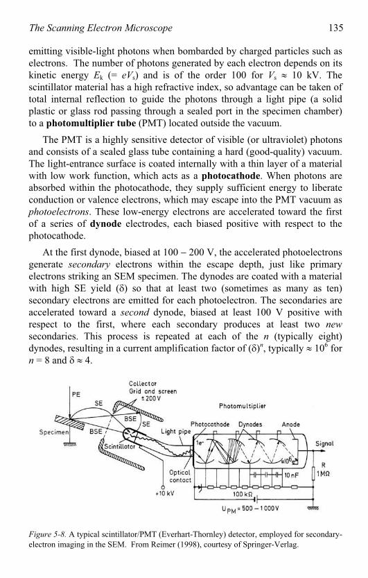
The Scanning Electron Microscope 135
emitting visible-light photons when bombarded by charged particles such as electrons. The number of photons generated by each electron depends on its kinetic energy Ek (= eVs) and is of the order 100 for Vs 10 kV. Thescintillator material has a high refractive index, so advantage can be taken of total internal reflection to guide the photons through a light pipe (a solid plastic or glass rod passing through a sealed port in the specimen chamber)to a photomultiplier tube (PMT) located outside the vacuum.
The PMT is a highly sensitive detector of visible (or ultraviolet) photonsand consists of a sealed glass tube containing a hard (good-quality) vacuum.The light-entrance surface is coated internally with a thin layer of a materialwith low work function, which acts as a photocathode. When photons are absorbed within the photocathode, they supply sufficient energy to liberate conduction or valence electrons, which may escape into the PMT vacuum as photoelectrons. These low-energy electrons are accelerated toward the firstof a series of dynode electrodes, each biased positive with respect to the photocathode.
At the first dynode, biased at 100 200 V, the accelerated photoelectronsgenerate secondary electrons within the escape depth, just like primary electrons striking an SEM specimen. The dynodes are coated with a materialwith high SE yield ( ) so that at least two (sometimes as many as ten) secondary electrons are emitted for each photoelectron. The secondaries areaccelerated toward a second dynode, biased at least 100 V positive with respect to the first, where each secondary produces at least two new
secondaries. This process is repeated at each of the n (typically eight) dynodes, resulting in a current amplification factor of ( )n, typically 106 for n = 8 and 4.
Figure 5-8. A typical scintillator/PMT (Everhart-Thornley) detector, employed for secondary-electron imaging in the SEM. From Reimer (1998), courtesy of Springer-Verlag.
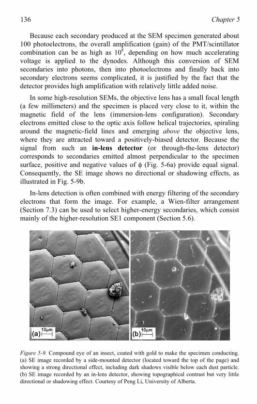
136 Chapter 5
Because each secondary produced at the SEM specimen generated about 100 photoelectrons, the overall amplification (gain) of the PMT/scintillatorcombination can be as high as 108, depending on how much acceleratingvoltage is applied to the dynodes. Although this conversion of SEM secondaries into photons, then into photoelectrons and finally back intosecondary electrons seems complicated, it is justified by the fact that the detector provides high amplification with relatively little added noise.
In some high-resolution SEMs, the objective lens has a small focal length (a few millimeters) and the specimen is placed very close to it, within the magnetic field of the lens (immersion-lens configuration). Secondaryelectrons emitted close to the optic axis follow helical trajectories, spiraling around the magnetic-field lines and emerging above the objective lens, where they are attracted toward a positively-biased detector. Because the signal from such an in-lens detector (or through-the-lens detector) corresponds to secondaries emitted almost perpendicular to the specimensurface, positive and negative values of (Fig. 5-6a) provide equal signal. Consequently, the SE image shows no directional or shadowing effects, as illustrated in Fig. 5-9b.
In-lens detection is often combined with energy filtering of the secondaryelectrons that form the image. For example, a Wien-filter arrangement(Section 7.3) can be used to select higher-energy secondaries, which consistmainly of the higher-resolution SE1 component (Section 5.6).
Figure 5-9. Compound eye of an insect, coated with gold to make the specimen conducting.(a) SE image recorded by a side-mounted detector (located toward the top of the page) andshowing a strong directional effect, including dark shadows visible below each dust particle.(b) SE image recorded by an in-lens detector, showing topographical contrast but very littledirectional or shadowing effect. Courtesy of Peng Li, University of Alberta.
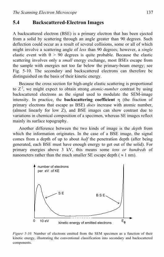
The Scanning Electron Microscope 137
5.4 Backscattered-Electron Images
A backscattered electron (BSE) is a primary electron that has been ejectedfrom a solid by scattering through an angle greater than 90 degrees. Suchdeflection could occur as a result of several collisions, some or all of whichmight involve a scattering angle of less than 90 degrees; however, a single
elastic event with > 90 degrees is quite probable. Because the elasticscattering involves only a small energy exchange, most BSEs escape fromthe sample with energies not too far below the primary-beam energy; seeFig. 5-10. The secondary and backscattered electrons can therefore be distinguished on the basis of their kinetic energy.
Because the cross section for high-angle elastic scattering is proportionalto Z 2, we might expect to obtain strong atomic-number contrast by usingbackscattered electrons as the signal used to modulate the SEM-imageintensity. In practice, the backscattering coefficient (the fraction of primary electrons that escape as BSE) does increase with atomic number,(almost linearly for low Z), and BSE images can show contrast due tovariations in chemical composition of a specimen, whereas SE images reflectmainly its surface topography.
Another difference between the two kinds of image is the depth from which the information originates. In the case of a BSE image, the signal comes from a depth of up to about half the penetration depth (after being generated, each BSE must have enough energy to get out of the solid). Forprimary energies above 3 kV, this means some tens or hundreds of nanometers rather than the much smaller SE escape depth ( 1 nm).
E0 kinetic energy of emitted electrons
10 eV
number of electrons
per eV of KE
S EB S E
0
Figure 5-10. Number of electrons emitted from the SEM specimen as a function of theirkinetic energy, illustrating the conventional classification into secondary and backscatteredcomponents.
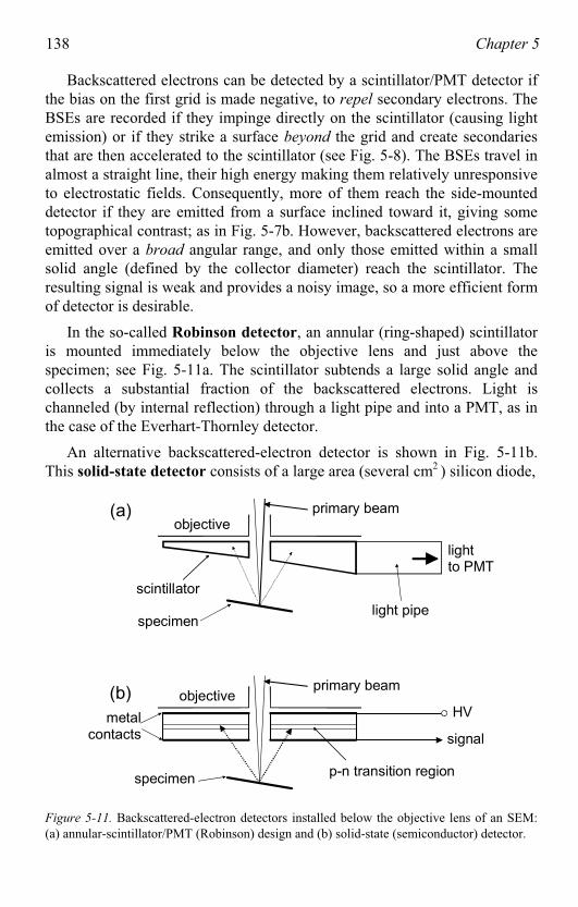
138 Chapter 5
Backscattered electrons can be detected by a scintillator/PMT detector if the bias on the first grid is made negative, to repel secondary electrons. The BSEs are recorded if they impinge directly on the scintillator (causing lightemission) or if they strike a surface beyond the grid and create secondaries that are then accelerated to the scintillator (see Fig. 5-8). The BSEs travel in almost a straight line, their high energy making them relatively unresponsiveto electrostatic fields. Consequently, more of them reach the side-mounteddetector if they are emitted from a surface inclined toward it, giving some topographical contrast; as in Fig. 5-7b. However, backscattered electrons are emitted over a broad angular range, and only those emitted within a small solid angle (defined by the collector diameter) reach the scintillator. Theresulting signal is weak and provides a noisy image, so a more efficient formof detector is desirable.
In the so-called Robinson detector, an annular (ring-shaped) scintillator is mounted immediately below the objective lens and just above the specimen; see Fig. 5-11a. The scintillator subtends a large solid angle and collects a substantial fraction of the backscattered electrons. Light ischanneled (by internal reflection) through a light pipe and into a PMT, as in the case of the Everhart-Thornley detector.
An alternative backscattered-electron detector is shown in Fig. 5-11b.This solid-state detector consists of a large area (several cm2 ) silicon diode,
scintillator
light pipespecimen
specimenp-n transition region
metalcontacts signal
HV
objective
objectiveprimary beam
primary beam(a)
(b)
lightto PMT
Figure 5-11. Backscattered-electron detectors installed below the objective lens of an SEM:(a) annular-scintillator/PMT (Robinson) design and (b) solid-state (semiconductor) detector.
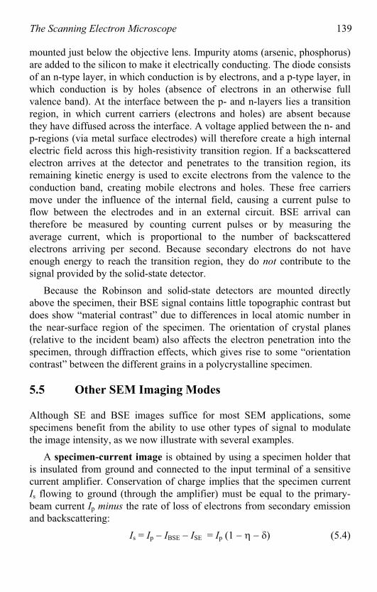
The Scanning Electron Microscope 139
mounted just below the objective lens. Impurity atoms (arsenic, phosphorus)are added to the silicon to make it electrically conducting. The diode consists of an n-type layer, in which conduction is by electrons, and a p-type layer, inwhich conduction is by holes (absence of electrons in an otherwise full valence band). At the interface between the p- and n-layers lies a transitionregion, in which current carriers (electrons and holes) are absent becausethey have diffused across the interface. A voltage applied between the n- and p-regions (via metal surface electrodes) will therefore create a high internalelectric field across this high-resistivity transition region. If a backscatteredelectron arrives at the detector and penetrates to the transition region, itsremaining kinetic energy is used to excite electrons from the valence to the conduction band, creating mobile electrons and holes. These free carriers move under the influence of the internal field, causing a current pulse toflow between the electrodes and in an external circuit. BSE arrival cantherefore be measured by counting current pulses or by measuring theaverage current, which is proportional to the number of backscatteredelectrons arriving per second. Because secondary electrons do not have enough energy to reach the transition region, they do not contribute to the signal provided by the solid-state detector.
Because the Robinson and solid-state detectors are mounted directly above the specimen, their BSE signal contains little topographic contrast but does show “material contrast” due to differences in local atomic number in the near-surface region of the specimen. The orientation of crystal planes (relative to the incident beam) also affects the electron penetration into the specimen, through diffraction effects, which gives rise to some “orientationcontrast” between the different grains in a polycrystalline specimen.
5.5 Other SEM Imaging Modes
Although SE and BSE images suffice for most SEM applications, somespecimens benefit from the ability to use other types of signal to modulatethe image intensity, as we now illustrate with several examples.
A specimen-current image is obtained by using a specimen holder that is insulated from ground and connected to the input terminal of a sensitivecurrent amplifier. Conservation of charge implies that the specimen current Is flowing to ground (through the amplifier) must be equal to the primary-beam current Ip minus the rate of loss of electrons from secondary emissionand backscattering:
Is = Ip IBSE ISE = Ip (1 ) (5.4)
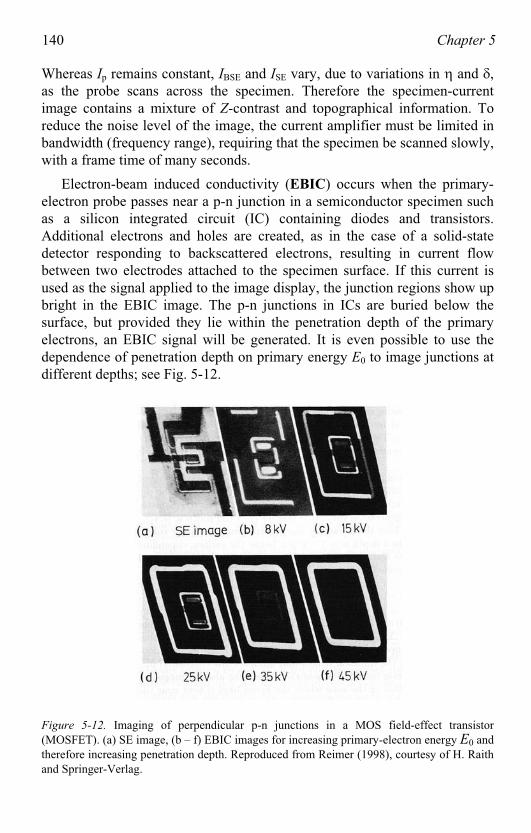
140 Chapter 5
Whereas Ip remains constant, IBSE and ISE vary, due to variations in and ,as the probe scans across the specimen. Therefore the specimen-currentimage contains a mixture of Z-contrast and topographical information. Toreduce the noise level of the image, the current amplifier must be limited in bandwidth (frequency range), requiring that the specimen be scanned slowly,
ith a frame time of many seconds.w
Electron-beam induced conductivity (EBIC) occurs when the primary-electron probe passes near a p-n junction in a semiconductor specimen such as a silicon integrated circuit (IC) containing diodes and transistors.Additional electrons and holes are created, as in the case of a solid-statedetector responding to backscattered electrons, resulting in current flow between two electrodes attached to the specimen surface. If this current isused as the signal applied to the image display, the junction regions show up bright in the EBIC image. The p-n junctions in ICs are buried below the surface, but provided they lie within the penetration depth of the primaryelectrons, an EBIC signal will be generated. It is even possible to use thedependence of penetration depth on primary energy E0 to image junctions atdifferent depths; see Fig. 5-12.
Figure 5-12. Imaging of perpendicular p-n junctions in a MOS field-effect transistor (MOSFET). (a) SE image, (b – f) EBIC images for increasing primary-electron energy E0 andtherefore increasing penetration depth. Reproduced from Reimer (1998), courtesy of H. Raithand Springer-Verlag.
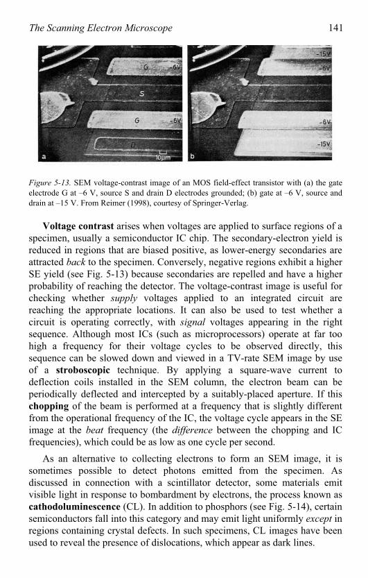
The Scanning Electron Microscope 141
Figure 5-13. SEM voltage-contrast image of an MOS field-effect transistor with (a) the gateelectrode G at –6 V, source S and drain D electrodes grounded; (b) gate at –6 V, source anddrain at –15 V. From Reimer (1998), courtesy of Springer-Verlag.
Voltage contrast arises when voltages are applied to surface regions of a specimen, usually a semiconductor IC chip. The secondary-electron yield isreduced in regions that are biased positive, as lower-energy secondaries areattracted back to the specimen. Conversely, negative regions exhibit a higherSE yield (see Fig. 5-13) because secondaries are repelled and have a higherprobability of reaching the detector. The voltage-contrast image is useful for checking whether supply voltages applied to an integrated circuit are reaching the appropriate locations. It can also be used to test whether a circuit is operating correctly, with signal voltages appearing in the rightsequence. Although most ICs (such as microprocessors) operate at far too high a frequency for their voltage cycles to be observed directly, this sequence can be slowed down and viewed in a TV-rate SEM image by useof a stroboscopic technique. By applying a square-wave current to deflection coils installed in the SEM column, the electron beam can beperiodically deflected and intercepted by a suitably-placed aperture. If thischopping of the beam is performed at a frequency that is slightly different from the operational frequency of the IC, the voltage cycle appears in the SEimage at the beat frequency (the difference between the chopping and ICfrequencies), which could be as low as one cycle per second.
As an alternative to collecting electrons to form an SEM image, it is sometimes possible to detect photons emitted from the specimen. As discussed in connection with a scintillator detector, some materials emit visible light in response to bombardment by electrons, the process known ascathodoluminescence (CL). In addition to phosphors (see Fig. 5-14), certain semiconductors fall into this category and may emit light uniformly except in regions containing crystal defects. In such specimens, CL images have beenused to reveal the presence of dislocations, which appear as dark lines.
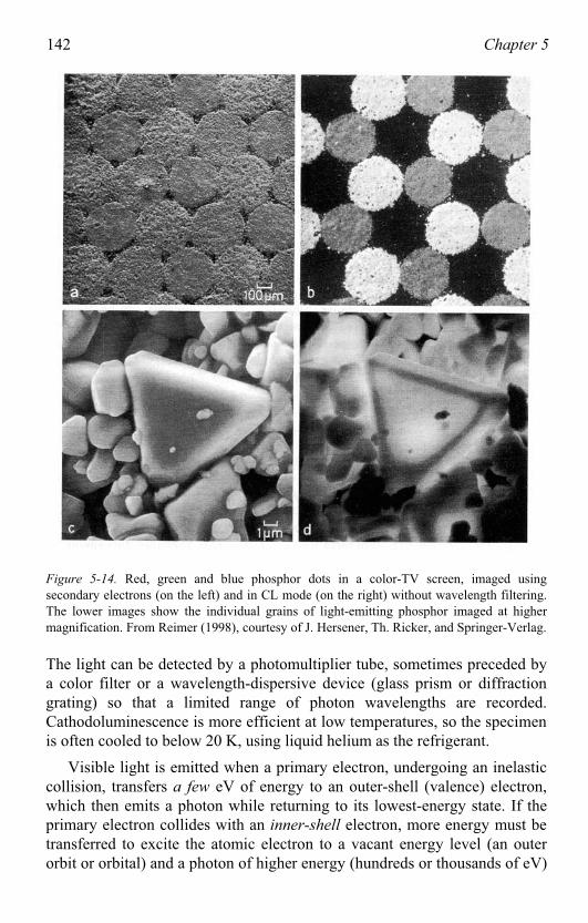
142 Chapter 5
Figure 5-14. Red, green and blue phosphor dots in a color-TV screen, imaged usingsecondary electrons (on the left) and in CL mode (on the right) without wavelength filtering.The lower images show the individual grains of light-emitting phosphor imaged at highermagnification. From Reimer (1998), courtesy of J. Hersener, Th. Ricker, and Springer-Verlag.
The light can be detected by a photomultiplier tube, sometimes preceded by a color filter or a wavelength-dispersive device (glass prism or diffractiongrating) so that a limited range of photon wavelengths are recorded.Cathodoluminescence is more efficient at low temperatures, so the specimens often cooled to below 20 K, using liquid helium as the refrigerant. i
Visible light is emitted when a primary electron, undergoing an inelasticcollision, transfers a few eV of energy to an outer-shell (valence) electron,which then emits a photon while returning to its lowest-energy state. If the primary electron collides with an inner-shell electron, more energy must betransferred to excite the atomic electron to a vacant energy level (an outer orbit or orbital) and a photon of higher energy (hundreds or thousands of eV)
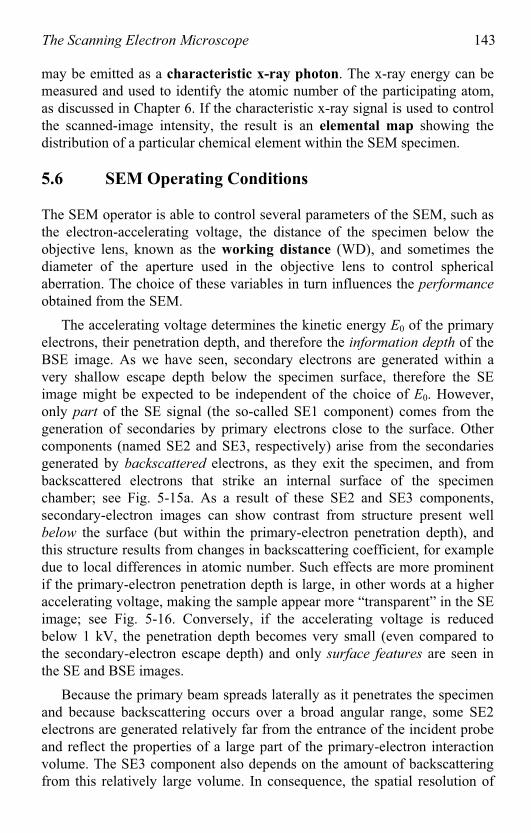
The Scanning Electron Microscope 143
may be emitted as a characteristic x-ray photon. The x-ray energy can bemeasured and used to identify the atomic number of the participating atom,as discussed in Chapter 6. If the characteristic x-ray signal is used to controlthe scanned-image intensity, the result is an elemental map showing the distribution of a particular chemical element within the SEM specimen.
5.6 SEM Operating Conditions
The SEM operator is able to control several parameters of the SEM, such asthe electron-accelerating voltage, the distance of the specimen below the objective lens, known as the working distance (WD), and sometimes thediameter of the aperture used in the objective lens to control spherical aberration. The choice of these variables in turn influences the performance
btained from the SEM.o
The accelerating voltage determines the kinetic energy E0 of the primaryelectrons, their penetration depth, and therefore the information depth of theBSE image. As we have seen, secondary electrons are generated within avery shallow escape depth below the specimen surface, therefore the SE image might be expected to be independent of the choice of E0. However, only part of the SE signal (the so-called SE1 component) comes from the generation of secondaries by primary electrons close to the surface. Othercomponents (named SE2 and SE3, respectively) arise from the secondaries generated by backscattered electrons, as they exit the specimen, and from backscattered electrons that strike an internal surface of the specimenchamber; see Fig. 5-15a. As a result of these SE2 and SE3 components,secondary-electron images can show contrast from structure present well below the surface (but within the primary-electron penetration depth), and this structure results from changes in backscattering coefficient, for exampledue to local differences in atomic number. Such effects are more prominentif the primary-electron penetration depth is large, in other words at a higher accelerating voltage, making the sample appear more “transparent” in the SE image; see Fig. 5-16. Conversely, if the accelerating voltage is reduced below 1 kV, the penetration depth becomes very small (even compared to the secondary-electron escape depth) and only surface features are seen in the SE and BSE images.
Because the primary beam spreads laterally as it penetrates the specimenand because backscattering occurs over a broad angular range, some SE2electrons are generated relatively far from the entrance of the incident probe and reflect the properties of a large part of the primary-electron interaction volume. The SE3 component also depends on the amount of backscatteringfrom this relatively large volume. In consequence, the spatial resolution of
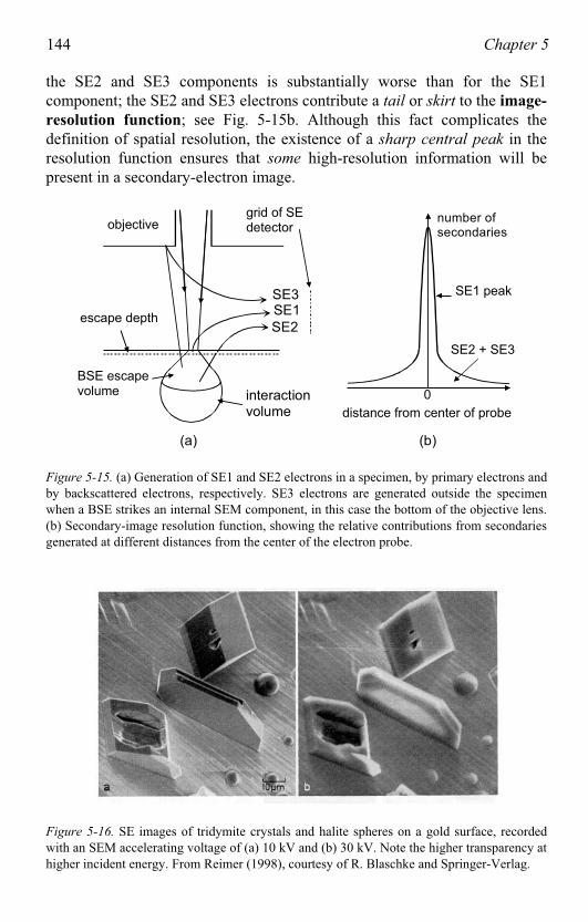
144 Chapter 5
the SE2 and SE3 components is substantially worse than for the SE1 component; the SE2 and SE3 electrons contribute a tail or skirt to the image-
resolution function; see Fig. 5-15b. Although this fact complicates the definition of spatial resolution, the existence of a sharp central peak in theresolution function ensures that some high-resolution information will bepresent in a secondary-electron image.
SE1
SE2
SE3
objective
escape depth
BSE escape volume interaction
volume
grid of SEdetector
0
number ofsecondaries
distance from center of probe
SE1 peak
SE2 + SE3
(a) (b)
Figure 5-15. (a) Generation of SE1 and SE2 electrons in a specimen, by primary electrons andby backscattered electrons, respectively. SE3 electrons are generated outside the specimenwhen a BSE strikes an internal SEM component, in this case the bottom of the objective lens. (b) Secondary-image resolution function, showing the relative contributions from secondariesgenerated at different distances from the center of the electron probe.
Figure 5-16. SE images of tridymite crystals and halite spheres on a gold surface, recordedwith an SEM accelerating voltage of (a) 10 kV and (b) 30 kV. Note the higher transparency athigher incident energy. From Reimer (1998), courtesy of R. Blaschke and Springer-Verlag.
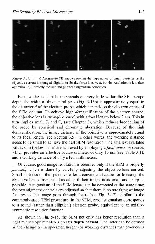
The Scanning Electron Microscope 145
Figure 5-17. (a – c) Astigmatic SE image showing the appearance of small particles as theobjective current is changed slightly; in (b) the focus is correct, but the resolution is less than optimum. (d) Correctly focused image after astigmatism correction.
Because the incident beam spreads out very little within the SE1 escapedepth, the width of this central peak (Fig. 5-15b) is approximately equal tothe diameter d of the electron probe, which depends on the electron optics of the SEM column. To achieve high demagnification of the electron source, the objective lens is strongly excited, with a focal length below 2 cm. This in turn implies small Cs and Cc (see Chapter 2), which reduces broadening of the probe by spherical and chromatic aberration. Because of the high demagnification, the image distance of the objective is approximately equal to its focal length (see Section 3.5); in other words, the working distanceneeds to be small to achieve the best SEM resolution. The smallest availablevalues of d (below 1 nm) are achieved by employing a field-emission source, which provides an effective source diameter of only 10 nm (see Table 3-1),and a working distance of only a few millimeters.
Of course, good image resolution is obtained only if the SEM is properlyfocused, which is done by carefully adjusting the objective-lens current. Small particles on the specimen offer a convenient feature for focusing; theobjective lens current is adjusted until their image is as small and sharp as possible. Astigmatism of the SEM lenses can be corrected at the same time;the two stigmator controls are adjusted so that there is no streaking of imagefeatures as the image goes through focus (see Fig. 5-17), similar to the commonly-used TEM procedure. In the SEM, zero astigmatism correspondsto a round (rather than elliptical) electron probe, equivalent to an axially-symmetric resolution function.
As shown in Fig. 5-18, the SEM not only has better resolution than alight microscope but also a greater depth of field. The latter can be definedas the change v in specimen height (or working distance) that produces a
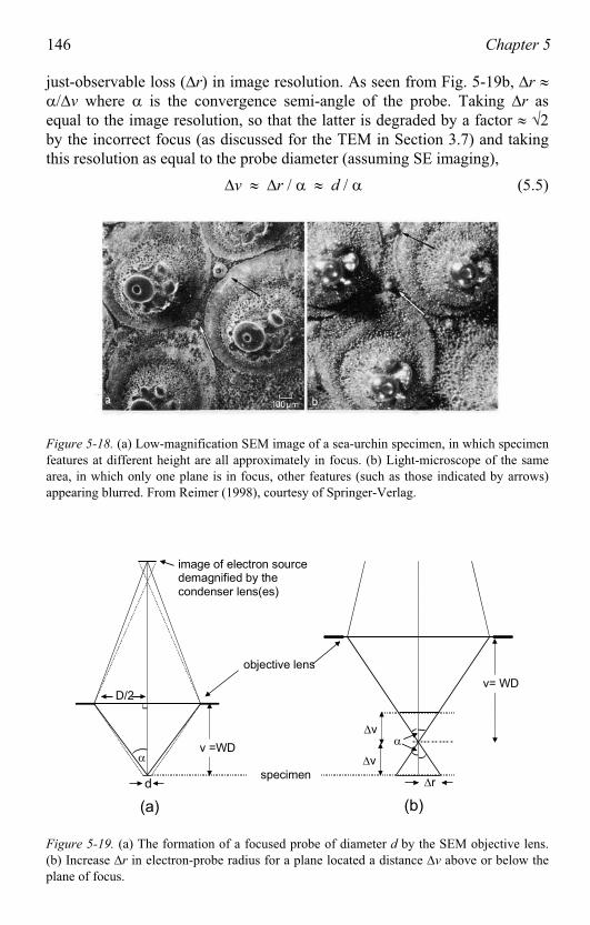
146 Chapter 5
just-observable loss ( r) in image resolution. As seen from Fig. 5-19b, r
/ v where is the convergence semi-angle of the probe. Taking r asequal to the image resolution, so that the latter is degraded by a factor 2by the incorrect focus (as discussed for the TEM in Section 3.7) and taking this resolution as equal to the probe diameter (assuming SE imaging),
v r / d / (5.5)
Figure 5-18. (a) Low-magnification SEM image of a sea-urchin specimen, in which specimenfeatures at different height are all approximately in focus. (b) Light-microscope of the samearea, in which only one plane is in focus, other features (such as those indicated by arrows)appearing blurred. From Reimer (1998), courtesy of Springer-Verlag.
v= WD
image of electron sourcedemagnified by thecondenser lens(es)
d
D/2
r
v
(a) (b)
objective lens
v =WDv
specimen
Figure 5-19. (a) The formation of a focused probe of diameter d by the SEM objective lens.(b) Increase r in electron-probe radius for a plane located a distance v above or below theplane of focus.
The Scanning Electron Microscope 147
The large SEM depth of field is seen to be a direct result of the relatively small convergence angle of the electron probe, which in turn is dictated bythe need to limit probe broadening due to spherical and chromatic aberration. As shown in Fig. 5-19a,
D/(2v) (5.6)
According to Eqs. (5.5) and (5.6), the depth of field v can be increased byincreasing v or reducing D , although in either case there may be some loss of resolution because of increased diffraction effects (see page 4). MostSEMs allow the working distance to be changed, by height adjustment of thespecimen relative to the lens column. Some microscopes also provide achoice of objective diaphragm, with apertures of more than one diameter.
Because of the large depth of field, the SEM specimen can be tiltedaway from the horizontal and toward the SE detector (to increase SE yield)without too much loss of resolution away from the center of the image. Even so, this effect can be reduced to zero (in principle) by a technique calleddynamic focusing. It involves applying the x- and/or y-scan signal (with an appropriate amplitude, which depends on the angle of tilt) to the objective-current power supply, in order to ensure that the specimen surface remains infocus at all times during the scan. This procedure can be regarded as anadaptation of Maxwell’s third rule of focusing (see Chapter 2) to deal with a non-perpendicular image plane. No similar option is available in the TEM, where the post-specimen lenses image all object points simultaneously.
5.7 SEM Specimen Preparation
One major advantage of the SEM (in comparison to a TEM) is the ease ofspecimen preparation, a result of the fact that the specimen does not have to be made thin. In fact, many conducting specimens require no special preparation before examination in the SEM. On the other hand, specimens of insulating materials do not provide a path to ground for the specimen current Is and may undergo electrostatic charging when exposed to the electron probe. As is evident from Eq. (5.4), this current can be of either sign,depending on the values of the backscattering coefficient and secondary-electron yield . Therefore, the local charge on the specimen can be positive or negative. Negative charge presents a more serious problem, as it repelsthe incident electrons and deflects the scanning probe, resulting in imagedistortion or fluctuations in image intensity.
One solution to the charging problem is to coat the surface of the SEM specimen with a thin film of metal or conducting carbon. This is done invacuum, using the evaporation or sublimation technique already discussed in
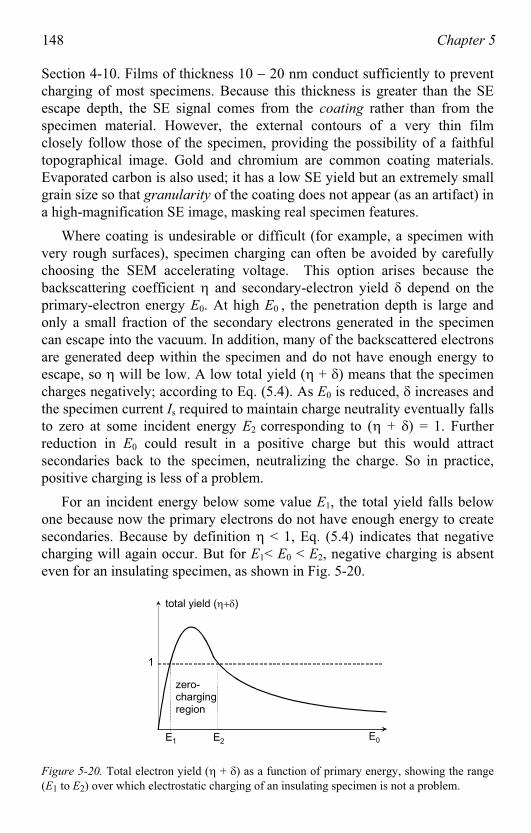
148 Chapter 5
Section 4-10. Films of thickness 10 20 nm conduct sufficiently to prevent charging of most specimens. Because this thickness is greater than the SE escape depth, the SE signal comes from the coating rather than from the specimen material. However, the external contours of a very thin film closely follow those of the specimen, providing the possibility of a faithful topographical image. Gold and chromium are common coating materials.Evaporated carbon is also used; it has a low SE yield but an extremely smallgrain size so that granularity of the coating does not appear (as an artifact) ina high-magnification SE image, masking real specimen features.
Where coating is undesirable or difficult (for example, a specimen with very rough surfaces), specimen charging can often be avoided by carefully choosing the SEM accelerating voltage. This option arises because the backscattering coefficient and secondary-electron yield depend on theprimary-electron energy E0. At high E0 , the penetration depth is large andonly a small fraction of the secondary electrons generated in the specimencan escape into the vacuum. In addition, many of the backscattered electrons are generated deep within the specimen and do not have enough energy toescape, so will be low. A low total yield ( + ) means that the specimencharges negatively; according to Eq. (5.4). As E0 is reduced, increases and the specimen current Is required to maintain charge neutrality eventually falls to zero at some incident energy E2 corresponding to ( + ) = 1. Furtherreduction in E0 could result in a positive charge but this would attractsecondaries back to the specimen, neutralizing the charge. So in practice, positive charging is less of a problem.
For an incident energy below some value E1, the total yield falls belowone because now the primary electrons do not have enough energy to create secondaries. Because by definition < 1, Eq. (5.4) indicates that negative charging will again occur. But for E1< E0 < E2, negative charging is absenteven for an insulating specimen, as shown in Fig. 5-20.
E0E1 E2
1
total yield ( )
zero-chargingregion
Figure 5-20. Total electron yield ( + ) as a function of primary energy, showing the range (E1 to E2) over which electrostatic charging of an insulating specimen is not a problem.
The Scanning Electron Microscope 149
Typically, E2 is in the range 1 10 keV. Although there are tables givingvalues for common materials (Joy and Joy, 1996), E2 is usually foundexperimentally, by reducing the accelerating voltage until charging artifacts(distortion or pulsating of the image) disappear. E1 is typically a few hundredvolts, below the normal range of SEM operation.
The use of low-voltage SEM is therefore a practical option for imaginginsulating specimens. The main disadvantage of low E0 is the increasedchromatic-aberration broadening of the electron probe, given approximatelyby rc = Cc ( E/E0). This problem can be minimized by using a field-emission source (which has a low energy spread: E < 0.5 eV) and by careful design of the objective lens to reduce the chromatic-aberrationcoefficient Cc. This is an area of continuing research and development.
5.8 The Environmental SEM
An alternative approach to overcoming the specimen-charging problem is tosurround the specimen with a gaseous ambient rather than high vacuum. Inthis situation, the primary electrons ionize gas molecules before reaching thespecimen. If the specimen charges negatively, positive ions are attractedtoward it, largely neutralizing the surface charge.
Of course, there must still be a good vacuum within the SEM column in order to allow the operation of a thermionic or field-emission source, to enable a high voltage to be used to accelerate the electrons and to permit the focusing of electrons without scattering from gas molecules. In anenvironmental SEM (also called a low-vacuum SEM), primary electronsencounter gas molecules only during the last few mm of their journey, after being focused by the objective lens. A small-diameter aperture in the bore ofthe objective allows the electrons to pass through but prevents most gas molecules from traveling up the SEM column. Those that do so are removedby continuous pumping. In some designs, a second pressure-differentialaperture is placed just below the electron gun, to allow an adequate vacuumto be maintained in the gun, which has its own vacuum pump.
The pressure in the sample chamber can be as high as 5000 Pa (0.05 atmosphere), although a few hundred Pascal is more typical. The gas surrounding the specimen is often water vapor, as this choice allows wet
specimens to be examined in the SEM without dehydration, provided thespecimen-chamber pressure exceeds the saturated vapor pressure (SVP) of water at the temperature of the specimen. At 25 C, the SVP of water is about 3000 Pa. However the required pressure can be reduced by a factor of 5 ormore by cooling the specimen, using a thermoelectric element incorporatedinto the specimen stage.
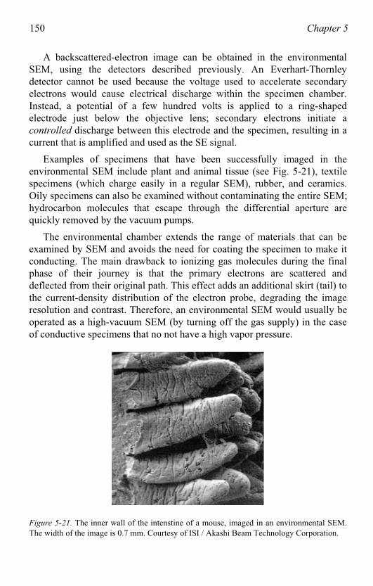
150 Chapter 5
A backscattered-electron image can be obtained in the environmentalSEM, using the detectors described previously. An Everhart-Thornleydetector cannot be used because the voltage used to accelerate secondaryelectrons would cause electrical discharge within the specimen chamber.Instead, a potential of a few hundred volts is applied to a ring-shaped electrode just below the objective lens; secondary electrons initiate a controlled discharge between this electrode and the specimen, resulting in a current that is amplified and used as the SE signal.
Examples of specimens that have been successfully imaged in theenvironmental SEM include plant and animal tissue (see Fig. 5-21), textilespecimens (which charge easily in a regular SEM), rubber, and ceramics.Oily specimens can also be examined without contaminating the entire SEM; hydrocarbon molecules that escape through the differential aperture are quickly removed by the vacuum pumps.
The environmental chamber extends the range of materials that can be examined by SEM and avoids the need for coating the specimen to make itconducting. The main drawback to ionizing gas molecules during the final phase of their journey is that the primary electrons are scattered and deflected from their original path. This effect adds an additional skirt (tail) tothe current-density distribution of the electron probe, degrading the image resolution and contrast. Therefore, an environmental SEM would usually beoperated as a high-vacuum SEM (by turning off the gas supply) in the case of conductive specimens that no not have a high vapor pressure.
Figure 5-21. The inner wall of the intenstine of a mouse, imaged in an environmental SEM.The width of the image is 0.7 mm. Courtesy of ISI / Akashi Beam Technology Corporation.
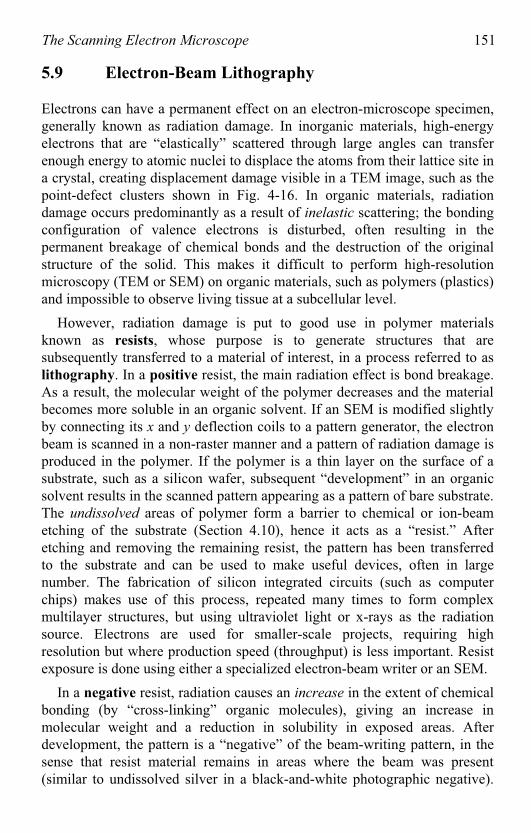
The Scanning Electron Microscope 151
5.9 Electron-Beam Lithography
Electrons can have a permanent effect on an electron-microscope specimen,generally known as radiation damage. In inorganic materials, high-energyelectrons that are “elastically” scattered through large angles can transfer enough energy to atomic nuclei to displace the atoms from their lattice site in a crystal, creating displacement damage visible in a TEM image, such as the point-defect clusters shown in Fig. 4-16. In organic materials, radiation damage occurs predominantly as a result of inelastic scattering; the bondingconfiguration of valence electrons is disturbed, often resulting in thepermanent breakage of chemical bonds and the destruction of the originalstructure of the solid. This makes it difficult to perform high-resolution microscopy (TEM or SEM) on organic materials, such as polymers (plastics)nd impossible to observe living tissue at a subcellular level. a
However, radiation damage is put to good use in polymer materialsknown as resists, whose purpose is to generate structures that are subsequently transferred to a material of interest, in a process referred to aslithography. In a positive resist, the main radiation effect is bond breakage.As a result, the molecular weight of the polymer decreases and the materialbecomes more soluble in an organic solvent. If an SEM is modified slightlyby connecting its x and y deflection coils to a pattern generator, the electron beam is scanned in a non-raster manner and a pattern of radiation damage is produced in the polymer. If the polymer is a thin layer on the surface of a substrate, such as a silicon wafer, subsequent “development” in an organicsolvent results in the scanned pattern appearing as a pattern of bare substrate.The undissolved areas of polymer form a barrier to chemical or ion-beam etching of the substrate (Section 4.10), hence it acts as a “resist.” Afteretching and removing the remaining resist, the pattern has been transferredto the substrate and can be used to make useful devices, often in largenumber. The fabrication of silicon integrated circuits (such as computerchips) makes use of this process, repeated many times to form complexmultilayer structures, but using ultraviolet light or x-rays as the radiation source. Electrons are used for smaller-scale projects, requiring high resolution but where production speed (throughput) is less important. Resistexposure is done using either a specialized electron-beam writer or an SEM.
In a negative resist, radiation causes an increase in the extent of chemicalbonding (by “cross-linking” organic molecules), giving an increase inmolecular weight and a reduction in solubility in exposed areas. Afterdevelopment, the pattern is a “negative” of the beam-writing pattern, in thesense that resist material remains in areas where the beam was present(similar to undissolved silver in a black-and-white photographic negative).
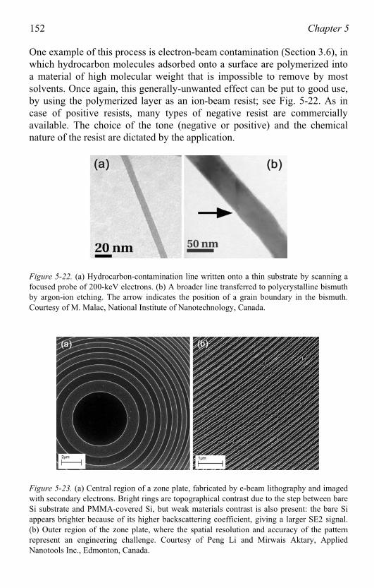
152 Chapter 5
One example of this process is electron-beam contamination (Section 3.6), in which hydrocarbon molecules adsorbed onto a surface are polymerized intoa material of high molecular weight that is impossible to remove by mostsolvents. Once again, this generally-unwanted effect can be put to good use,by using the polymerized layer as an ion-beam resist; see Fig. 5-22. As in case of positive resists, many types of negative resist are commerciallyavailable. The choice of the tone (negative or positive) and the chemicalnature of the resist are dictated by the application.
Figure 5-22. (a) Hydrocarbon-contamination line written onto a thin substrate by scanning a focused probe of 200-keV electrons. (b) A broader line transferred to polycrystalline bismuthby argon-ion etching. The arrow indicates the position of a grain boundary in the bismuth.Courtesy of M. Malac, National Institute of Nanotechnology, Canada.
Figure 5-23. (a) Central region of a zone plate, fabricated by e-beam lithography and imagedwith secondary electrons. Bright rings are topographical contrast due to the step between bareSi substrate and PMMA-covered Si, but weak materials contrast is also present: the bare Siappears brighter because of its higher backscattering coefficient, giving a larger SE2 signal.(b) Outer region of the zone plate, where the spatial resolution and accuracy of the patternrepresent an engineering challenge. Courtesy of Peng Li and Mirwais Aktary, AppliedNanotools Inc., Edmonton, Canada.
The Scanning Electron Microscope 153
For microelectronics and nanotechnology applications, patterns must be generated on a very fine scale, and the spatial resolution of the pattern is of prime concern. Electrons can be focused into a probe of very small diameter,but when they penetrate a thick solid, the beam spreads laterally (Fig. 5-3), and so the backscattered electrons (which affect a resist coating the surface)cause a loss in resolution, just as in secondary-electron imaging. One solution is to use a thin substrate in which backscattering is minimal,allowing line widths as small as 10 nm; see Fig. 5-22. Another option is to use electrons of low incident energy, where the penetration and lateral spreading of the beam in the substrate are small. In addition to electronicsapplications, a recent use of electron-beam lithography has been to fabricate zone plates for focusing x-rays; see Fig. 5-23.
Chapter 6
ANALYTICAL ELECTRON MICROSCOPY
The TEM and SEM techniques described in earlier chapters yield valuableinformation about the external or internal structure of a specimen, but little about its chemical composition. Some of the phenomena involved (diffracted electrons in TEM, BSE in the SEM) depend on the local atomic number Z,but not to an extent that would enable us to distinguish between adjacentelements in the periodic table. For that purpose, we need a signal that ishighly Z-specific; for example, an effect that involves the electron-shell structure of an atom. Clearly, the latter is element-specific because itdetermines the position of each element in the periodic table.
6.1 The Bohr Model of the Atom
A scientific model provides a means of accounting for the properties of an object, preferably using familiar concepts. To understand the electron-shell structure of an atom, we will use the semi-classical description of an atom given by Niels Bohr in 1913. Bohr's concept resembles the Rutherfordplanetary model insofar as it assumes the atom to consist of a central nucleus (charge = +Ze) surrounded by electrons that behave as particles (charge e
and mass m). The attractive Coulomb force exerted on an electron (by the nucleus) supplies the centripetal force necessary to keep the electron in a ircular orbit of radius r:c
K (Ze)(e) /r 2 = mv 2/r (6.1)
Here, K = 1/(4 0) is the Coulomb constant and v is the tangential speed of the electron. The Bohr model differs from that of Rutherford by introducing
requirement that the orbit is allowed only if it satisfies the condition: a
(mv) r = n (h/2 ) (6.2)
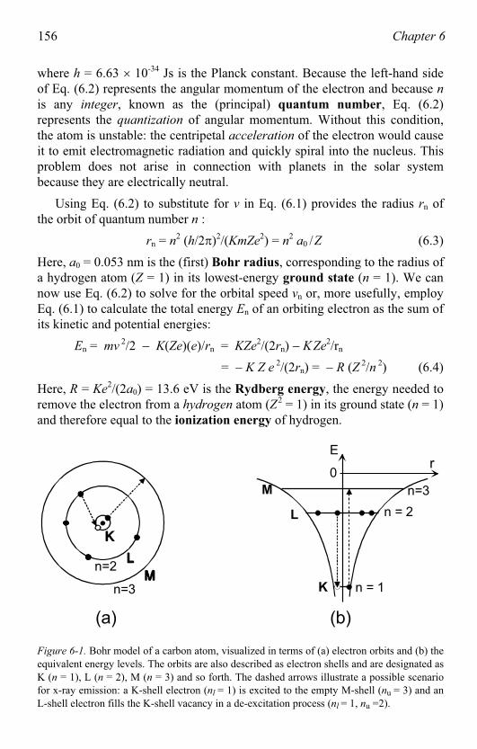
156 Chapter 6
where h = 6.63 10-34 Js is the Planck constant. Because the left-hand side of Eq. (6.2) represents the angular momentum of the electron and because nis any integer, known as the (principal) quantum number, Eq. (6.2)represents the quantization of angular momentum. Without this condition, the atom is unstable: the centripetal acceleration of the electron would causeit to emit electromagnetic radiation and quickly spiral into the nucleus. This problem does not arise in connection with planets in the solar systemecause they are electrically neutral. b
Using Eq. (6.2) to substitute for v in Eq. (6.1) provides the radius rn of he orbit of quantum number n : t
rn = n2 (h/2 )2/(KmZe2) = n2 a0 /Z (6.3)
Here, a0 = 0.053 nm is the (first) Bohr radius, corresponding to the radius ofa hydrogen atom (Z = 1) in its lowest-energy ground state (n = 1). We cannow use Eq. (6.2) to solve for the orbital speed vn or, more usefully, employEq. (6.1) to calculate the total energy En of an orbiting electron as the sum ofts kinetic and potential energies:i
En = mv 2/2 K(Ze)(e)/rn = KZe2/(2rn) KZe2/rn
= K Z e 2/(2rn) = R (Z 2/n 2) (6.4)
Here, R = Ke2/(2a0) = 13.6 eV is the Rydberg energy, the energy needed to remove the electron from a hydrogen atom (Z2 = 1) in its ground state (n = 1)and therefore equal to the ionization energy of hydrogen.
K n = 1
n = 2
n=3
0
Er
L
M
n=3
n=2
(a) (b)
Figure 6-1. Bohr model of a carbon atom, visualized in terms of (a) electron orbits and (b) theequivalent energy levels. The orbits are also described as electron shells and are designated asK (n = 1), L (n = 2), M (n = 3) and so forth. The dashed arrows illustrate a possible scenariofor x-ray emission: a K-shell electron (nl = 1) is excited to the empty M-shell (nu = 3) and anL-shell electron fills the K-shell vacancy in a de-excitation process (nl = 1, nu =2).
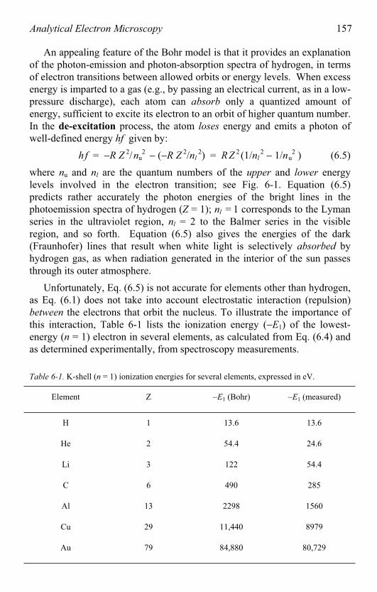
Analytical Electron Microscopy 157
An appealing feature of the Bohr model is that it provides an explanation of the photon-emission and photon-absorption spectra of hydrogen, in terms of electron transitions between allowed orbits or energy levels. When excessenergy is imparted to a gas (e.g., by passing an electrical current, as in a low-pressure discharge), each atom can absorb only a quantized amount of energy, sufficient to excite its electron to an orbit of higher quantum number.In the de-excitation process, the atom loses energy and emits a photon of well-defined energy hf given by:
h f = R Z 2/nu2 ( R Z 2/nl
2) = RZ 2 (1/nl2 1/nu
2 ) (6.5)
where nu and nl are the quantum numbers of the upper and lower energy levels involved in the electron transition; see Fig. 6-1. Equation (6.5) predicts rather accurately the photon energies of the bright lines in the photoemission spectra of hydrogen (Z = 1); nl = 1 corresponds to the Lymanseries in the ultraviolet region, nl = 2 to the Balmer series in the visible region, and so forth. Equation (6.5) also gives the energies of the dark(Fraunhofer) lines that result when white light is selectively absorbed by hydrogen gas, as when radiation generated in the interior of the sun passesthrough its outer atmosphere.
Unfortunately, Eq. (6.5) is not accurate for elements other than hydrogen, as Eq. (6.1) does not take into account electrostatic interaction (repulsion)between the electrons that orbit the nucleus. To illustrate the importance of this interaction, Table 6-1 lists the ionization energy ( E1) of the lowest-energy (n = 1) electron in several elements, as calculated from Eq. (6.4) and as determined experimentally, from spectroscopy measurements.
Table 6-1. K-shell (n = 1) ionization energies for several elements, expressed in eV.
Element Z E1 (Bohr) E1 (measured)
H 1 13.6 13.6
He 2 54.4 24.6
Li 3 122 54.4
C 6 490 285
Al 13 2298 1560
Cu 29 11,440 8979
Au 79 84,880 80,729
158 Chapter 6
Many-electron atoms represent a difficult theoretical problem because, ina classical (particle) model, the distance between the different orbiting electrons is always changing. In any event, a more realistic conception of theatom uses wave mechanics, treating the atomic electrons as de Broglie
waves. Analysis then involves solving the Schrödinger wave equation to determine the electron wavefunctions, represented by orbitals (pictured as charge-density clouds) that replace the concept of particle orbits. An exact solution is possible for hydrogen and results in binding energies that are identical to those predicted by Eq. (6.4). Approximate methods are used forthe other elements, and in many cases the calculated energy levels are reasonably close to those determined from optical spectroscopy.
Other wave-mechanical principles determine the maximum number of electrons in each atomic shell: 2 for the innermost K-shell, 8 for the L-shell,18 for the M-shell and so forth. Because an atom in its ground state represents the minimum-energy configuration, electrons fill these shells insequence (with increasing atomic number), starting with the K-shell.
As indicated by Table 6-1, the measured energy levels differ substantiallybetween different elements, resulting in photon energies (always a difference
in energy between two atomic shells) that can be used to identify each element. Except for H, He, and Li, these photon energies are above 100 eVand lie within the x-ray region of the electromagnetic spectrum.
6.2 X-ray Emission Spectroscopy
When a primary electron enters a TEM or SEM specimen, it has a (small)probability of being scattered inelastically by an inner-shell (e.g. K-shell) electron, causing the latter to undergo a transition to a higher-energy orbit(or wave-mechanical state) and leaving the atom with an electron vacancy(hole) in its inner shell. However, the scattering atom remains in this excited
state for only a very brief period of time: within about 10-15 s, one of the other atomic electrons fills the inner-shell vacancy by making a downward
transition from a higher energy level, as in Fig. 6-1b. In this de-excitationprocess, energy can be released in the form of a photon whose energy (hf ) is given roughly by Eq. (6.5) but more accurately by the actual difference inbinding energy between the upper and lower levels.
The energy of this characteristic x-ray photon therefore depends on the atomic number Z of the atom involved and on the quantum numbers (nl , nu)of the energy levels involved in the electron transition. Characteristic x-rayscan be classified according to the following historical scheme. The electronshell in which the original inner-shell vacancy was created, which corresponds to the quantum number nl , is represented by an upper-case
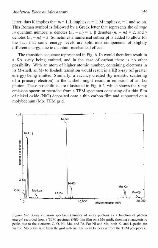
Analytical Electron Microscopy 159
letter; thus K implies that nl = 1, L implies nl = 1, M implies nl = 1 and so on.This Roman symbol is followed by a Greek letter that represents the change
in quantum number: denotes (nu nl) = 1, denotes (nu nl) = 2, and denotes (nu nl) = 3. Sometimes a numerical subscript is added to allow forthe fact that some energy levels are split into components of slightlydifferent energy, due to quantum-mechanical effects.
The transition sequence represented in Fig. 6-1b would therefore result in a K x-ray being emitted, and in the case of carbon there is no other possibility. With an atom of higher atomic number, containing electrons inits M-shell, an M- to K-shell transition would result in a K x-ray (of greaterenergy) being emitted. Similarly, a vacancy created (by inelastic scatteringof a primary electron) in the L-shell might result in emission of an Lphoton. These possibilities are illustrated in Fig. 6-2, which shows the x-rayemission spectrum recorded from a TEM specimen consisting of a thin filmof nickel oxide (NiO) deposited onto a thin carbon film and supported on a molybdenum (Mo) TEM grid.
Figure 6-2. X-ray emission spectrum (number of x-ray photons as a function of photonenergy) recorded from a TEM specimen (NiO thin film on a Mo grid), showing characteristicpeaks due to the elements C, O, Ni, Mo, and Fe. For Ni and Mo, both K- and L-peaks arevisible. Mo peaks arise from the grid material; the weak Fe peak is from the TEM polepieces.
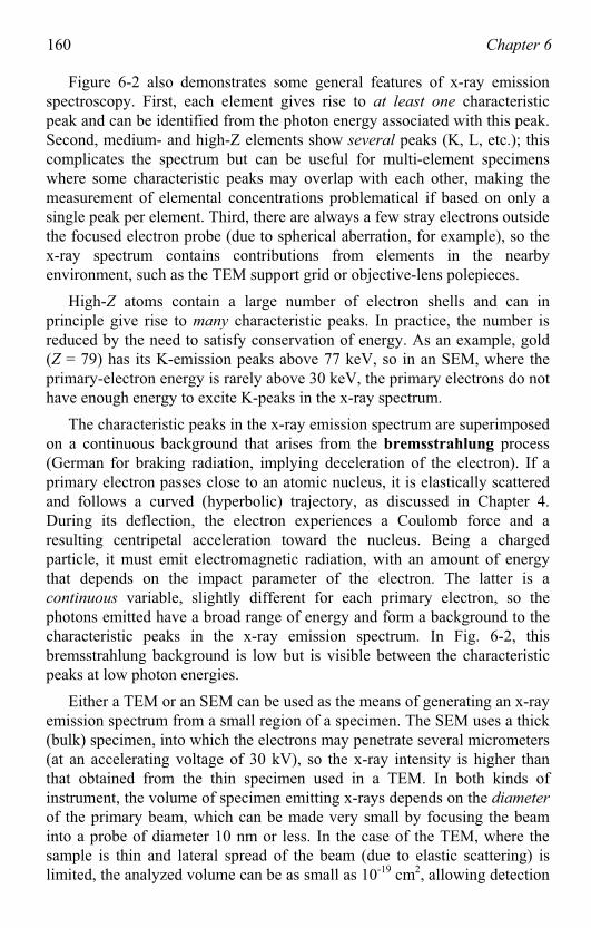
160 Chapter 6
Figure 6-2 also demonstrates some general features of x-ray emissionspectroscopy. First, each element gives rise to at least one characteristicpeak and can be identified from the photon energy associated with this peak. Second, medium- and high-Z elements show several peaks (K, L, etc.); thiscomplicates the spectrum but can be useful for multi-element specimenswhere some characteristic peaks may overlap with each other, making themeasurement of elemental concentrations problematical if based on only a single peak per element. Third, there are always a few stray electrons outside the focused electron probe (due to spherical aberration, for example), so the x-ray spectrum contains contributions from elements in the nearby environment, such as the TEM support grid or objective-lens polepieces.
High-Z atoms contain a large number of electron shells and can in principle give rise to many characteristic peaks. In practice, the number isreduced by the need to satisfy conservation of energy. As an example, gold (Z = 79) has its K-emission peaks above 77 keV, so in an SEM, where the primary-electron energy is rarely above 30 keV, the primary electrons do nothave enough energy to excite K-peaks in the x-ray spectrum.
The characteristic peaks in the x-ray emission spectrum are superimposedon a continuous background that arises from the bremsstrahlung process(German for braking radiation, implying deceleration of the electron). If aprimary electron passes close to an atomic nucleus, it is elastically scatteredand follows a curved (hyperbolic) trajectory, as discussed in Chapter 4.During its deflection, the electron experiences a Coulomb force and aresulting centripetal acceleration toward the nucleus. Being a charged particle, it must emit electromagnetic radiation, with an amount of energythat depends on the impact parameter of the electron. The latter is a continuous variable, slightly different for each primary electron, so the photons emitted have a broad range of energy and form a background to thecharacteristic peaks in the x-ray emission spectrum. In Fig. 6-2, this bremsstrahlung background is low but is visible between the characteristic peaks at low photon energies.
Either a TEM or an SEM can be used as the means of generating an x-ray emission spectrum from a small region of a specimen. The SEM uses a thick (bulk) specimen, into which the electrons may penetrate several micrometers(at an accelerating voltage of 30 kV), so the x-ray intensity is higher than that obtained from the thin specimen used in a TEM. In both kinds ofinstrument, the volume of specimen emitting x-rays depends on the diameter
of the primary beam, which can be made very small by focusing the beaminto a probe of diameter 10 nm or less. In the case of the TEM, where thesample is thin and lateral spread of the beam (due to elastic scattering) islimited, the analyzed volume can be as small as 10-19 cm2, allowing detection
Analytical Electron Microscopy 161
of less than 10-19 g of an element. In the SEM, x-rays are emitted from theentire interaction volume, which becomes larger as the incident energy of the electrons is increased (Fig. 5-3).
To generate a spectrum from the emitted x-rays, we need some form of dispersive device that distinguishes x-ray photons on the basis of either their energy (E = hf, where f is the frequency of the electromagnetic wave) ortheir wavelength ( = c/f = hc/E, where c is the speed of light in vacuum).Although photon energy and wavelength are closely related, these twooptions give rise to two distinct forms of spectroscopy, which we discuss inSections 6.3 and 6.6.
6.3 X-ray Energy-Dispersive Spectroscopy
In x-ray energy-dispersive spectroscopy (XEDS), the dispersive device is a semiconductor diode, fabricated from a single crystal of silicon (or germanium) and somewhat similar to the BSE detector in an SEM. If an x-ray photon enters and penetrates to the transition region (between p- and n-doped material), its energy can release a considerable number of outer-shell(valence) electrons from the confinement of a particular atomic nucleus. Thisprocess is equivalent to exciting electrons from the valence to the conductionband (i.e,. the creation of electron-hole pairs) and results in electricalconduction by both electrons and holes for a brief period of time. With a reverse-bias voltage applied to the diode, this conduction causes electricalcharge to flow through the junction (and around an external circuit), thecharge being proportional to the number N of electron-hole pairs generated. Assuming that all of the photon energy (hf ) goes into creating electron-hole(e-h) pairs, each pair requiring an average energy E, energy conservation implies:
N = hf / E (6.6)
For silicon, E 4 eV (just over twice the energy gap between valence andconduction bands), therefore a Cu-K photon creates about (8000eV)/(4eV)= 2000 e-h pairs.
To ensure that essentially all of the incoming x-rays are absorbed and generate current pulses in an external circuit, the p-n transition region ismade much wider than in most semiconductor diodes. In the case of silicon, this can be done by diffusing in the element lithium (Z = 3), which annihilates the effect of other electrically-active (dopant) impurities andcreates a high-resistivity (intrinsic) region several mm in width; see Fig. 6-3.
If the semiconductor diode were operated at room temperature, thermal
generation of electron-hole pairs would contribute too much electronic noise
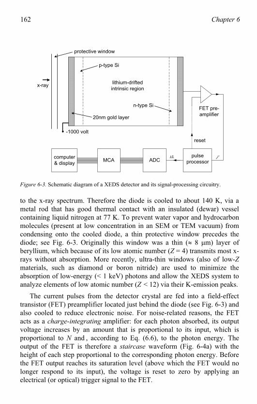
162 Chapter 6
20nm gold layer
lithium-drifted
intrinsic region
FET pre-
amplifier
p-type Si
n-type Si
-1000 volt
protective window
x-ray
MCApulse
processorADCcomputer
& display
reset
Figure 6-3. Schematic diagram of a XEDS detector and its signal-processing circuitry.
to the x-ray spectrum. Therefore the diode is cooled to about 140 K, via a metal rod that has good thermal contact with an insulated (dewar) vesselcontaining liquid nitrogen at 77 K. To prevent water vapor and hydrocarbonmolecules (present at low concentration in an SEM or TEM vacuum) fromcondensing onto the cooled diode, a thin protective window precedes the diode; see Fig. 6-3. Originally this window was a thin ( 8 m) layer ofberyllium, which because of its low atomic number (Z = 4) transmits most x-rays without absorption. More recently, ultra-thin windows (also of low-Zmaterials, such as diamond or boron nitride) are used to minimize theabsorption of low-energy (< 1 keV) photons and allow the XEDS system to analyze elements of low atomic number (Z < 12) via their K-emission peaks.
The current pulses from the detector crystal are fed into a field-effecttransistor (FET) preamplifier located just behind the diode (see Fig. 6-3) and also cooled to reduce electronic noise. For noise-related reasons, the FETacts as a charge-integrating amplifier: for each photon absorbed, its outputvoltage increases by an amount that is proportional to its input, which is proportional to N and , according to Eq. (6.6), to the photon energy. Theoutput of the FET is therefore a staircase waveform (Fig. 6-4a) with the height of each step proportional to the corresponding photon energy. Before the FET output reaches its saturation level (above which the FET would no longer respond to its input), the voltage is reset to zero by applying anelectrical (or optical) trigger signal to the FET.
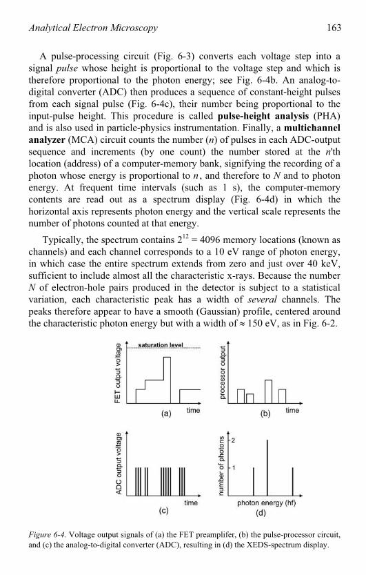
Analytical Electron Microscopy 163
A pulse-processing circuit (Fig. 6-3) converts each voltage step into a signal pulse whose height is proportional to the voltage step and which istherefore proportional to the photon energy; see Fig. 6-4b. An analog-to-digital converter (ADC) then produces a sequence of constant-height pulses from each signal pulse (Fig. 6-4c), their number being proportional to theinput-pulse height. This procedure is called pulse-height analysis (PHA)and is also used in particle-physics instrumentation. Finally, a multichannel
analyzer (MCA) circuit counts the number (n) of pulses in each ADC-outputsequence and increments (by one count) the number stored at the n'thlocation (address) of a computer-memory bank, signifying the recording of a photon whose energy is proportional to n , and therefore to N and to photonenergy. At frequent time intervals (such as 1 s), the computer-memorycontents are read out as a spectrum display (Fig. 6-4d) in which thehorizontal axis represents photon energy and the vertical scale represents the number of photons counted at that energy.
Typically, the spectrum contains 212 = 4096 memory locations (known as channels) and each channel corresponds to a 10 eV range of photon energy,in which case the entire spectrum extends from zero and just over 40 keV, sufficient to include almost all the characteristic x-rays. Because the numberN of electron-hole pairs produced in the detector is subject to a statisticalvariation, each characteristic peak has a width of several channels. Thepeaks therefore appear to have a smooth (Gaussian) profile, centered around the characteristic photon energy but with a width of 150 eV, as in Fig. 6-2.
Figure 6-4. Voltage output signals of (a) the FET preamplifer, (b) the pulse-processor circuit,and (c) the analog-to-digital converter (ADC), resulting in (d) the XEDS-spectrum display.
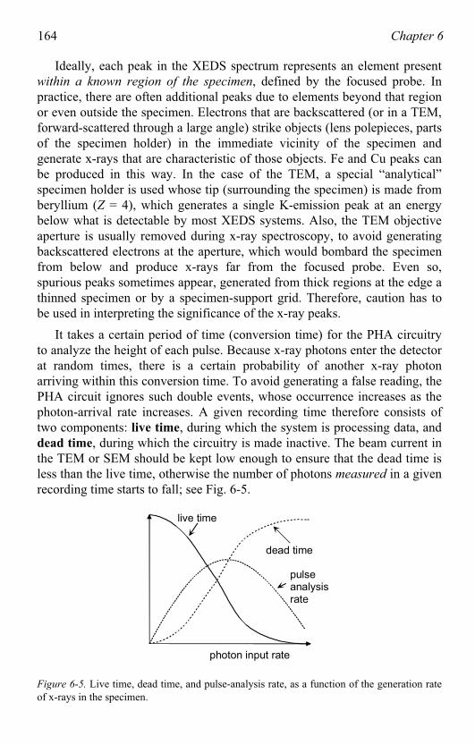
164 Chapter 6
Ideally, each peak in the XEDS spectrum represents an element presentwithin a known region of the specimen, defined by the focused probe. Inpractice, there are often additional peaks due to elements beyond that region or even outside the specimen. Electrons that are backscattered (or in a TEM, forward-scattered through a large angle) strike objects (lens polepieces, partsof the specimen holder) in the immediate vicinity of the specimen andgenerate x-rays that are characteristic of those objects. Fe and Cu peaks canbe produced in this way. In the case of the TEM, a special “analytical”specimen holder is used whose tip (surrounding the specimen) is made fromberyllium (Z = 4), which generates a single K-emission peak at an energybelow what is detectable by most XEDS systems. Also, the TEM objectiveaperture is usually removed during x-ray spectroscopy, to avoid generatingbackscattered electrons at the aperture, which would bombard the specimenfrom below and produce x-rays far from the focused probe. Even so, spurious peaks sometimes appear, generated from thick regions at the edge a thinned specimen or by a specimen-support grid. Therefore, caution has tobe used in interpreting the significance of the x-ray peaks.
It takes a certain period of time (conversion time) for the PHA circuitryto analyze the height of each pulse. Because x-ray photons enter the detector at random times, there is a certain probability of another x-ray photon arriving within this conversion time. To avoid generating a false reading, the PHA circuit ignores such double events, whose occurrence increases as the photon-arrival rate increases. A given recording time therefore consists oftwo components: live time, during which the system is processing data, anddead time, during which the circuitry is made inactive. The beam current in the TEM or SEM should be kept low enough to ensure that the dead time is less than the live time, otherwise the number of photons measured in a givenrecording time starts to fall; see Fig. 6-5.
live time
dead time
pulseanalysisrate
photon input rate
Figure 6-5. Live time, dead time, and pulse-analysis rate, as a function of the generation rate of x-rays in the specimen.
Analytical Electron Microscopy 165
The time taken to record a useful XEDS spectrum is dictated by the needto clearly identify the position of each significant peak (its characteristicenergy) and also, for measurement of elemental ratios, the total number of
photon counts in each peak (the peak integral or area). If the recording timeis too short, an insufficient number of x-ray photons will be analyzed and the spectrum will be “noisy.” This electronic noise arises from the fact that thegeneration of x-rays in the specimen is a statistical process, giving rise to astatistical variation in the number of counts per channel in the XEDS spectrum. According to the rules of (Poisson) statistics, if N randomly-arriving photons are recorded, we can expect a variation in that number (the standard deviation) equal to N1/2 if the experiment were repeated many times.The accuracy of measuring N is therefore N1/2 and the fractional accuracy is N1/2/N = N
-1/2 = 0.1 for N = 100. As a result, we need at least 100 x-raycounts in a characteristic peak in order to measure the concentration of thecorresponding element to an accuracy of 10%. Typically, this conditionimplies a recording time of at least 10 s, and sometimes several minutes ifthe x-ray generation rate is low (e.g., with a thin specimen in the TEM).
One important feature of XEDS analysis is that it can provide aquantitative estimate of the concentration ratios of elements present in aspecimen. The first requirement is to determine the number of characteristicx-ray photons contributing to each peak, by measuring the area (integral) of the peak and subtracting a contribution from the bremsstrahlung background.This background contribution is estimated by measuring the background on either side of the peak, then interpolating or (for greater accuracy) fitting the background to some simple mathematical function. However, the ratio of two peak integrals is not equal to the ratio of the elemental concentrations, as x-rays are not emitted with equal efficiency by different elements. The physics of x-ray production is simplest for the case of a very thin specimen,as used in the TEM, so we consider this situation first.
6.4 Quantitative Analysis in the TEM
For quantification, we need an equation that relates the number NA of x-rayphotons contributing to a characteristic peak of an element A to its concentration nA (number of atoms of element A per unit volume). We canexpect NA to be proportional to the number Ne of electrons that pass throughthe sample during the XEDS recording time, and to the product nAt, where tis the specimen thickness (for thin specimens, the probability of inner-shellinelastic scattering increases proportional to t).
However, the product nAt (termed the areal density of the element) hasdimensions of m-2, whereas NA and Ne are dimensionless numbers. In order
166 Chapter 6
to balance the units in our equation, there must be an additional factor whose dimensions are m2. This factor is the ionization cross section A for creatinga vacancy in an inner shell of element A. Such a cross section can beinterpreted as a target area for inelastic scattering of an incident electron by the atom, as discussed Section 4.3. The value of A depends on the type ofinner shell (K, L, etc.) as well as on the atomic number of the element.
Still missing from our equation is a factor known as the fluorescence
yield that allows for the fact that not every inner-shell vacancy gives rise tothe emission of an x-ray photon during the de-excitation of the atom. An alternative process allows the excited atom to return to its ground state by donating energy to another electron within the atom, which is ejected as an Auger electron (named after its discoverer, Pierre Auger). For elements of low atomic number, this Auger process is the more probable outcome andtheir x-ray fluorescence yield is considerably less than one ( << 1.0).
A remaining factor, known as the collection efficiency, , of the XEDSdetector, reflects the fact that x-ray photons are emitted equally in all directions; they travel in straight-line paths and only a fraction of them reach the detector. Combining all of these factors, the number of x-ray photons contributing to the characteristic peak of an element A is
NA = (nA t) A A Ne (6.7)
Applying the same considerations to some other element B present in the sample, we could generate a second equation, identical to Eq. (6.7) but withsubscripts B. Dividing Eq. (6.7) by this second equation, we obtain anexpression for the concentration ratio of the two elements:
nA/nB = [( B B)/( A A)] (NA/NB) (6.8)
The coefficient in square brackets is known as the k-factor of element A relative to element B. Although it is possible to calculate this k-factor fromtabulated ionization cross sections and fluorescence yields, a more accuratevalue is obtained by measuring the peak-intensity ratio (NA/NB) in aspectrum recorded from a “standard” sample (such as a binary compound)whose concentration ratio (nA/nB) is known. This measured k-factor will alsoinclude any difference in collection efficiency between element A andelement B (due to different absorption of x-rays in the detector window, for exa ple).m
The use of standards is common in analytical chemistry. But because thek-factor method was developed by metallurgists, the concentration ratio inEq. (6.8) usually represents a weight ratio of two elements, rather than the atomic ratio nA/nB , and k-factors reflect this convention. Such k-factors have been measured and tabulated for most elements but their precise values
Analytical Electron Microscopy 167
depend on the electron energy and detector design, so they are best measuredusing the same TEM/XEDS system as used for microanalysis. By analyzingcharacteristic peaks in pairs, the ratios of all elements in a multi-elementspecimen can be obtained from the measured peak integrals, knowing theappropriate k-factors. For further details, see Williams and Carter (1996).
6.5 Quantitative Analysis in the SEM
In an SEM, electrons enter a thick specimen and penetrate a certain distance, which can exceed 1 m (Section 5.2). Quantification is then complicated by the fact that many of the generated x-rays are absorbed before they leave the specimen. The amount of absorption depends on the chemical composition
of the specimen, which is generally unknown (otherwise there is no need for microanalysis). However, x-ray absorption coefficients have been measuredor calculated (as a function of photon energy) for all the chemical elements and are published in graphical or tabulated form. A legitimate procedure is therefore to initially assume no absorption of x-ray photons, by employing aprocedure based on Eq. (6.8) to estimate the ratios of all of the elements in the specimen, then to use these ratios to estimate the x-ray absorption thatought to have occurred in the specimen. Correcting the measured intensitiesfor absorption leads to a revised chemical composition, which can then beused to calculate absorption more accurately, and so on. After performingseveral cycles of this iterative procedure, the calculated elemental ratiosshould converge toward their true values.
Another complication is x-ray fluorescence, a process in which x-ray photons are absorbed but generate photons of lower energy. These lower-energy photons can contribute spurious intensity to a characteristic peak, changing the measured elemental ratio. Again, the effect can be calculated, but only if the chemical composition of the specimen is known. The solutionis therefore to include fluorescence corrections, as well as absorption, in the iterative process described above. Because the ionization cross sections andyields are Z-dependent, the whole procedure is known as ZAF correction
(making allowance for atomic number, absorption, and fluorescence) and is carried out by running a ZAF program on the computer that handles the acquisition and display of the x-ray emission spectrum.
6.6 X-ray Wavelength-Dispersive Spectroscopy
In x-ray wavelength-dispersive spectroscopy (XWDS), characteristic x-raysare distinguished on the basis of their wavelength rather than their photonenergy. This is done by taking advantage of the fact that a crystal behaves as
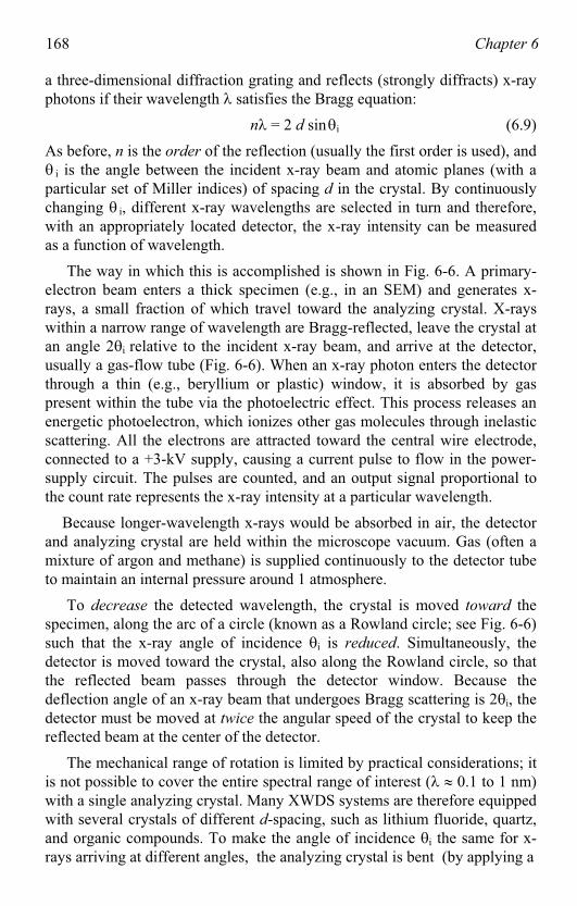
168 Chapter 6
a three-dimensional diffraction grating and reflects (strongly diffracts) x-ray photons if their wavelength satisfies the Bragg equation:
n = 2 d sin i (6.9)
As before, n is the order of the reflection (usually the first order is used), and
i is the angle between the incident x-ray beam and atomic planes (with a particular set of Miller indices) of spacing d in the crystal. By continuouslychanging i, different x-ray wavelengths are selected in turn and therefore,with an appropriately located detector, the x-ray intensity can be measuredas a function of wavelength.
The way in which this is accomplished is shown in Fig. 6-6. A primary-electron beam enters a thick specimen (e.g., in an SEM) and generates x-rays, a small fraction of which travel toward the analyzing crystal. X-rayswithin a narrow range of wavelength are Bragg-reflected, leave the crystal atan angle 2 i relative to the incident x-ray beam, and arrive at the detector,usually a gas-flow tube (Fig. 6-6). When an x-ray photon enters the detector through a thin (e.g., beryllium or plastic) window, it is absorbed by gaspresent within the tube via the photoelectric effect. This process releases anenergetic photoelectron, which ionizes other gas molecules through inelasticscattering. All the electrons are attracted toward the central wire electrode,connected to a +3-kV supply, causing a current pulse to flow in the power-supply circuit. The pulses are counted, and an output signal proportional tothe count rate represents the x-ray intensity at a particular wavelength.
Because longer-wavelength x-rays would be absorbed in air, the detectorand analyzing crystal are held within the microscope vacuum. Gas (often amixture of argon and methane) is supplied continuously to the detector tube to maintain an internal pressure around 1 atmosphere.
To decrease the detected wavelength, the crystal is moved toward the specimen, along the arc of a circle (known as a Rowland circle; see Fig. 6-6) such that the x-ray angle of incidence i is reduced. Simultaneously, thedetector is moved toward the crystal, also along the Rowland circle, so that the reflected beam passes through the detector window. Because thedeflection angle of an x-ray beam that undergoes Bragg scattering is 2 i, the detector must be moved at twice the angular speed of the crystal to keep thereflected beam at the center of the detector.
The mechanical range of rotation is limited by practical considerations; it is not possible to cover the entire spectral range of interest ( 0.1 to 1 nm)with a single analyzing crystal. Many XWDS systems are therefore equippedwith several crystals of different d-spacing, such as lithium fluoride, quartz, and organic compounds. To make the angle of incidence i the same for x-rays arriving at different angles, the analyzing crystal is bent (by applying a
Analytical Electron Microscopy 169
+3kV
electron
beam
x-rays
specimen
crystal
detector
Rowland
circle
Figure 6-6. Schematic diagram of an XWDS system. For simplicity, the Bragg-reflectingplanes are shown as being parallel to the surface of the analyzing crystal. The crystal anddetector move around the Rowland circle (dashed) in order to record the spectrum.
mechanical force) into a slightly-curved shape, which also provides a degreeof focusing similar to that of a concave mirror; see Fig. 6-6.
Although XWDS can be performed by adding the appropriate mechanical and electronic systems to an SEM, there exists a more specializedinstrument, the electron-probe microanalyzer (EPMA), which is optimizedfor such work. It generates an electron probe with substantial current, as required to record an x-ray spectrum with good statistics (low noise) within a reasonable time period. The EPMA is fitted with several analyzer/detectorassemblies so that more than a single wavelength range can be recordedsimultaneously.
6.7 Comparison of XEDS and XWDS Analysis
A big advantage of the XEDS technique is the speed of data acquisition, duelargely to the fact that x-rays within a wide energy range are detected andanalyzed simultaneously. In contrast, the XWDS system examines only onewavelength at any one time and may take several minutes to scan the required wavelength range. The XEDS detector can be brought very close (within a few mm) of the specimen, allowing about 1% of the emitted x-rays
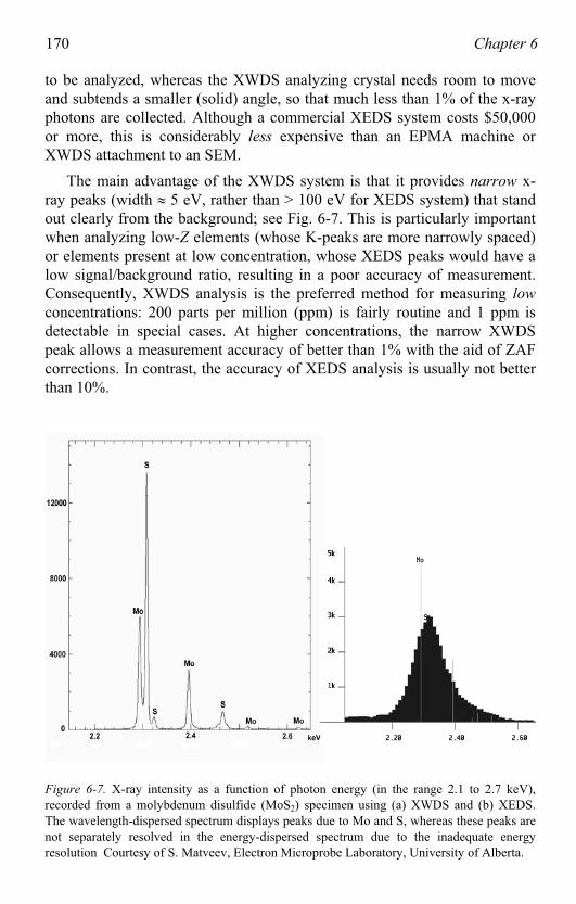
170 Chapter 6
to be analyzed, whereas the XWDS analyzing crystal needs room to moveand subtends a smaller (solid) angle, so that much less than 1% of the x-ray photons are collected. Although a commercial XEDS system costs $50,000or more, this is considerably less expensive than an EPMA machine or
WDS attachment to an SEM.X
The main advantage of the XWDS system is that it provides narrow x-ray peaks (width 5 eV, rather than > 100 eV for XEDS system) that stand out clearly from the background; see Fig. 6-7. This is particularly importantwhen analyzing low-Z elements (whose K-peaks are more narrowly spaced) or elements present at low concentration, whose XEDS peaks would have a low signal/background ratio, resulting in a poor accuracy of measurement.Consequently, XWDS analysis is the preferred method for measuring low
concentrations: 200 parts per million (ppm) is fairly routine and 1 ppm is detectable in special cases. At higher concentrations, the narrow XWDS peak allows a measurement accuracy of better than 1% with the aid of ZAF corrections. In contrast, the accuracy of XEDS analysis is usually not better than 10%.
Figure 6-7. X-ray intensity as a function of photon energy (in the range 2.1 to 2.7 keV), recorded from a molybdenum disulfide (MoS2) specimen using (a) XWDS and (b) XEDS. The wavelength-dispersed spectrum displays peaks due to Mo and S, whereas these peaks arenot separately resolved in the energy-dispersed spectrum due to the inadequate energyresolution Courtesy of S. Matveev, Electron Microprobe Laboratory, University of Alberta.
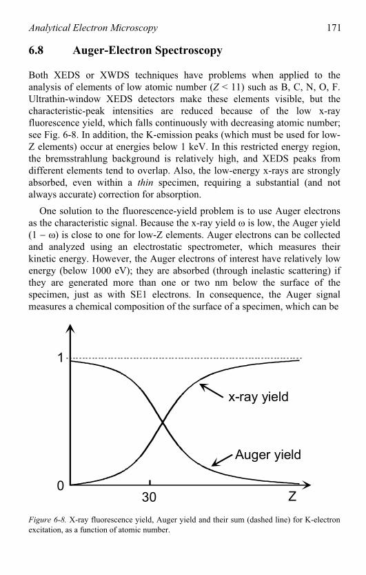
Analytical Electron Microscopy 171
6.8 Auger-Electron Spectroscopy
Both XEDS or XWDS techniques have problems when applied to theanalysis of elements of low atomic number (Z < 11) such as B, C, N, O, F.Ultrathin-window XEDS detectors make these elements visible, but thecharacteristic-peak intensities are reduced because of the low x-ray fluorescence yield, which falls continuously with decreasing atomic number;see Fig. 6-8. In addition, the K-emission peaks (which must be used for low-Z elements) occur at energies below 1 keV. In this restricted energy region, the bremsstrahlung background is relatively high, and XEDS peaks fromdifferent elements tend to overlap. Also, the low-energy x-rays are stronglyabsorbed, even within a thin specimen, requiring a substantial (and not lways accurate) correction for absorption. a
One solution to the fluorescence-yield problem is to use Auger electronsas the characteristic signal. Because the x-ray yield is low, the Auger yield (1 ) is close to one for low-Z elements. Auger electrons can be collectedand analyzed using an electrostatic spectrometer, which measures theirkinetic energy. However, the Auger electrons of interest have relatively lowenergy (below 1000 eV); they are absorbed (through inelastic scattering) if they are generated more than one or two nm below the surface of thespecimen, just as with SE1 electrons. In consequence, the Auger signalmeasures a chemical composition of the surface of a specimen, which can be
Z
1
0
x-ray yield
Auger yield
30
Figure 6-8. X-ray fluorescence yield, Auger yield and their sum (dashed line) for K-electron excitation, as a function of atomic number.
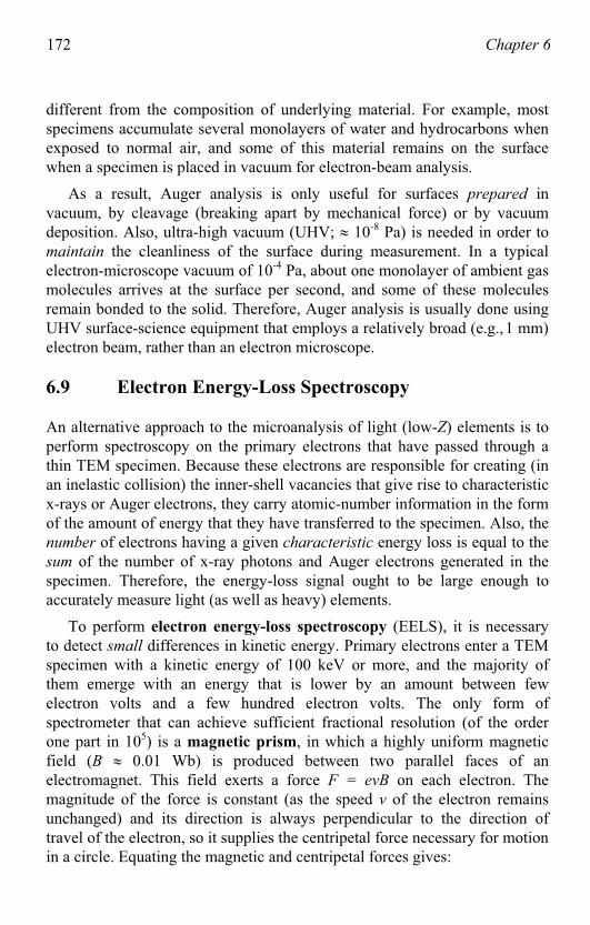
172 Chapter 6
different from the composition of underlying material. For example, mostspecimens accumulate several monolayers of water and hydrocarbons whenexposed to normal air, and some of this material remains on the surfacewhen a specimen is placed in vacuum for electron-beam analysis.
As a result, Auger analysis is only useful for surfaces prepared in vacuum, by cleavage (breaking apart by mechanical force) or by vacuum deposition. Also, ultra-high vacuum (UHV; 10-8 Pa) is needed in order tomaintain the cleanliness of the surface during measurement. In a typicalelectron-microscope vacuum of 10-4 Pa, about one monolayer of ambient gas molecules arrives at the surface per second, and some of these moleculesremain bonded to the solid. Therefore, Auger analysis is usually done usingUHV surface-science equipment that employs a relatively broad (e.g.,1 mm)electron beam, rather than an electron microscope.
6.9 Electron Energy-Loss Spectroscopy
An alternative approach to the microanalysis of light (low-Z) elements is to perform spectroscopy on the primary electrons that have passed through a thin TEM specimen. Because these electrons are responsible for creating (in an inelastic collision) the inner-shell vacancies that give rise to characteristicx-rays or Auger electrons, they carry atomic-number information in the form of the amount of energy that they have transferred to the specimen. Also, the number of electrons having a given characteristic energy loss is equal to the sum of the number of x-ray photons and Auger electrons generated in the specimen. Therefore, the energy-loss signal ought to be large enough toaccurately measure light (as well as heavy) elements.
To perform electron energy-loss spectroscopy (EELS), it is necessaryto detect small differences in kinetic energy. Primary electrons enter a TEMspecimen with a kinetic energy of 100 keV or more, and the majority ofthem emerge with an energy that is lower by an amount between few electron volts and a few hundred electron volts. The only form of spectrometer that can achieve sufficient fractional resolution (of the order one part in 105) is a magnetic prism, in which a highly uniform magneticfield (B 0.01 Wb) is produced between two parallel faces of anelectromagnet. This field exerts a force F = evB on each electron. The magnitude of the force is constant (as the speed v of the electron remainsunchanged) and its direction is always perpendicular to the direction of travel of the electron, so it supplies the centripetal force necessary for motionin a circle. Equating the magnetic and centripetal forces gives:
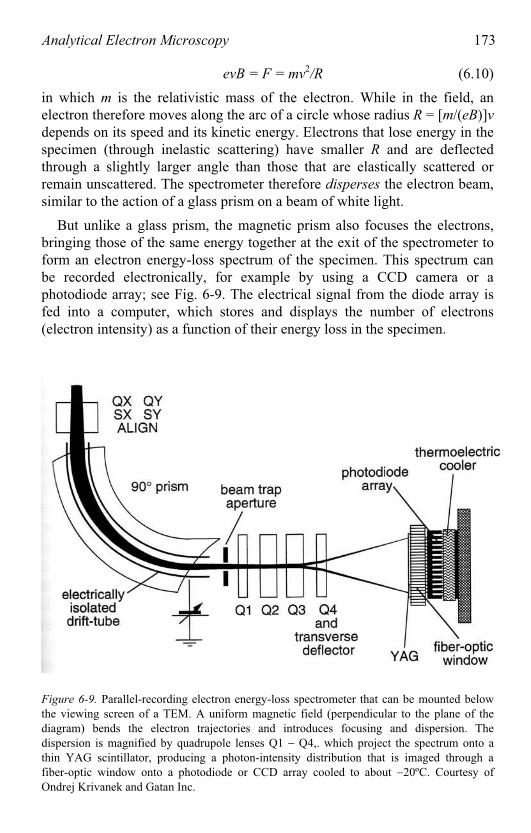
Analytical Electron Microscopy 173
evB = F = mv2/R (6.10)
in which m is the relativistic mass of the electron. While in the field, an electron therefore moves along the arc of a circle whose radius R = [m/(eB)]vdepends on its speed and its kinetic energy. Electrons that lose energy in the specimen (through inelastic scattering) have smaller R and are deflectedthrough a slightly larger angle than those that are elastically scattered orremain unscattered. The spectrometer therefore disperses the electron beam,imilar to the action of a glass prism on a beam of white light.s
But unlike a glass prism, the magnetic prism also focuses the electrons,bringing those of the same energy together at the exit of the spectrometer to form an electron energy-loss spectrum of the specimen. This spectrum canbe recorded electronically, for example by using a CCD camera or aphotodiode array; see Fig. 6-9. The electrical signal from the diode array is fed into a computer, which stores and displays the number of electrons (electron intensity) as a function of their energy loss in the specimen.
Figure 6-9. Parallel-recording electron energy-loss spectrometer that can be mounted belowthe viewing screen of a TEM. A uniform magnetic field (perpendicular to the plane of the diagram) bends the electron trajectories and introduces focusing and dispersion. The dispersion is magnified by quadrupole lenses Q1 Q4,. which project the spectrum onto a thin YAG scintillator, producing a photon-intensity distribution that is imaged through a fiber-optic window onto a photodiode or CCD array cooled to about 20ºC. Courtesy ofOndrej Krivanek and Gatan Inc.
174 Chapter 6
A typical energy-loss spectrum (Fig. 6-10) contains a zero-loss peak,representing electrons that were scattered elastically or remained unscattered
while passing through the specimen. Below 50 eV, one or more peaks represent inelastic scattering by outer-shell (valence or conduction) electrons in the specimen. This scattering can take the form of a collective oscillation (resonance) of many outer-shell electrons, known as a plasmon excitation. Inelastic excitation of inner-shell electrons causes an abrupt increase in electron intensity (an ionization edge) at an energy loss equal to an inner-shell ionization energy. Because this ionization energy is characteristic of aparticular chemical element and is known for every electron shell, the energyof each ionization edge indicates which elements are present within the specimen. Beyond each ionization threshold, the spectral intensity decaysmore gradually toward the (extrapolated) pre-edge background that arises from electron shells of lower ionization energy. The energy-loss intensity can be integrated over a region of typically 50 100 eV and the backgroundcomponent subtracted to give a signal IA that is proportional to theconcentration of the element A that gives rise to the edge. In fact, theconcentration ratio of two different elements (A , B) is given by:
nA/nB = (IA/IB) ( B / A) (6.11)
where A and B are ionization cross sections that can be calculated,knowing the atomic number, type of shell, and the integration range used for ach element.e
Because the magnetic prism has focusing properties, an electronspectrometer can be incorporated into the TEM imaging system and used toform an image from electrons that have undergone a particular energy loss in the specimen. Choosing this energy loss to correspond to the ionization edge of a known element, it is possible to form an elemental map that representshe distribution of that element, with a spatial resolution down to about 1 nm.t
Other information is present in the low-loss region of the spectrum(below 50 eV). In a single-scattering approximation, the amount of inelastic scattering is proportional to specimen thickness, as in Eq. (4.16). Therefore,the intensity of the plasmon peak relative to the zero-loss peak (Fig. 6-10)can be used to measure the local thickness at a known location in a TEM pecimen.s
Also, the energy-loss spectrum contains detailed information about theatomic arrangement and chemical bonding in the specimen, present in theform of fine structure in the low loss region and the ionization edges. For example, the intensities of the two sharp peaks at the onset of the Ba M-edgein Fig. 6-10 can be used to determine the charge state (valency) of thebarium atoms. For further details, see Brydson (2001) and Egerton (1996).
Analytical Electron Microscopy 175
Figure 6-10. Electron energy-loss spectrum of a high-temperature superconductor, showingN- and M-shell ionization edges of barium, the K-ionization edge of oxygen, and weakionization edges from copper and yttrium. The plasmon peak represents inelastic scatteringfrom valence electrons. A logarithmic vertical scale has been used in order to accommodatethe large range of electron intensity. Courtesy of D.H. Shin (Ph.D. thesis, Cornell University).
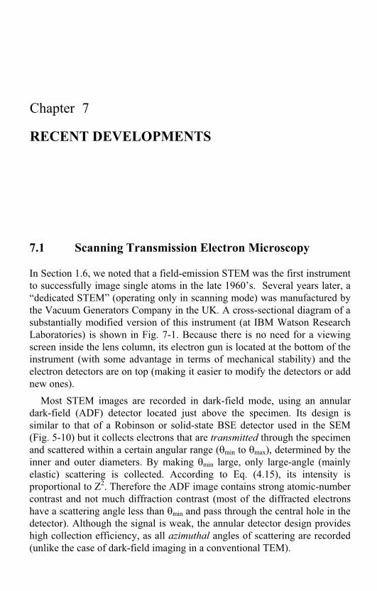
Chapter 7
RECENT DEVELOPMENTS
7.1 Scanning Transmission Electron Microscopy
In Section 1.6, we noted that a field-emission STEM was the first instrumentto successfully image single atoms in the late 1960’s. Several years later, a “dedicated STEM” (operating only in scanning mode) was manufactured by the Vacuum Generators Company in the UK. A cross-sectional diagram of asubstantially modified version of this instrument (at IBM Watson ResearchLaboratories) is shown in Fig. 7-1. Because there is no need for a viewing screen inside the lens column, its electron gun is located at the bottom of the instrument (with some advantage in terms of mechanical stability) and the electron detectors are on top (making it easier to modify the detectors or add ew ones).n
Most STEM images are recorded in dark-field mode, using an annulardark-field (ADF) detector located just above the specimen. Its design issimilar to that of a Robinson or solid-state BSE detector used in the SEM (Fig. 5-10) but it collects electrons that are transmitted through the specimen and scattered within a certain angular range ( min to max), determined by the inner and outer diameters. By making min large, only large-angle (mainlyelastic) scattering is collected. According to Eq. (4.15), its intensity isproportional to Z2. Therefore the ADF image contains strong atomic-numbercontrast and not much diffraction contrast (most of the diffracted electrons have a scattering angle less than min and pass through the central hole in thedetector). Although the signal is weak, the annular detector design provides high collection efficiency, as all azimuthal angles of scattering are recorded(unlike the case of dark-field imaging in a conventional TEM).

178 Chapter 7
Figure 7-1. Modified VG HB-501 STEM fitted with a gun monochromator, 120-kV Nionspherical-aberration corrector, ADF detector, and aberration-corrected electron spectrometer.Courtesy of Phil Batson, IBM Watson Research Laboratory, and Ondrej Krivanek, Nion Co.
Recent Developments 179
Figure 7-2. (a) ADF-STEM image of a catalyst specimen, showing individual Pt atoms on the surface of an alumina support; the circles indicate Pt3 trimers. Courtesy of R.D. Adams andM. Amiridis, University of South Carolina, A. Borisevich and S. Pennycook, Oak Ridge National Laboratory. (b) Image of a silicon crystal recorded with the electron beam parallel to(112), showing pairs of atomic columns 0.078 nm apart. Courtesy of Matthew F. Chisholm, ORNL, reprinted with permission from Science 305 (2004) 1741; copyright 2004 AAAS. Both of these images were recorded using the aberration-corrected VG603 STEM at ORNL.
Because the dedicated STEM has a field-emission source and a stronglyexcited objective lens (low Cs), it can form a probe of diameter 0.2 nm,offering the possibility of single-atom resolution. One area of application has been the study of the structure of catalysts, which typically consist of verymall metal particles on an oxide support; see Fig. 7-2a. s
The STEM can also produce atomic-resolution images of crystallinespecimens. If the specimen is oriented with a low-index crystal axis parallelto the incident beam, columns of atoms can be resolved (Fig. 7-2b), as in thecase of phase-contrast TEM images. However, the ADF detector provides an amplitude (scattering-contrast) signal that is relatively insensitive to the objective-lens focus; there are no contrast reversals (Section 4.9) and themage is more directly interpretable in terms of atomic coordinates. i
As shown in Fig. 7-1, the STEM is usually fitted with an energy-lossspectrometer that forms a spectrum from electrons (with scattering angle upto min) that pass through a central hole in the ADF detector. Thisarrangement allows dark-field and energy-filtered bright-field images to be recorded simultaneously. Also, after recording an atomic-resolution ADF image, the electron probe can be set to a precisely known location on thespecimen and the electron spectrometer used to provide elemental or fine-structure analysis with a spatial resolution down to the atomic level(Browning et al., 1997).
180 Chapter 7
7.2 Aberration Correction
From analysis of the basic properties of electric and magnetic fields, the German scientist Otto Scherzer showed that a conventional electron lens (where the magnetic or electrostatic fields have axial symmetry) must suffer from spherical and chromatic aberration, with aberration coefficients that are always positive. Therefore, we cannot eliminate lens aberrations by careful shaping of the lens polepieces, unlike the situation in light optics where aspherical lenses can be fabricated with zero Cs. In addition, it is not possible (in electron optics) to design compound lenses in which axially-symmetric lens elements have positive and negative aberration coefficients, o that they compensate for each other. s
Because of the practical incentive to achieve better resolution, physicists have for many years sought ways to circumvent Scherzer’s rule. One option is to employ mirror optics. An electrostatic mirror involves an electrode connected to a potential more negative than that of the electron source. Before reaching the electrode, electrons are brought to rest and their trajectory is reversed. As a result of this reversal of path, the mirror has negative aberration coefficients and can be used as a compensating element. By assembling an electron-optical system containing electrostatic lenses and an electrostatic mirror, Rempfer et al. (1997) showed that both spherical and chromatic aberrations can be corrected, for angles up to 40 mrad. Although no TEM or SEM has made use of this principle, it is being applied to the photoelectron microscope, in which electrons released from a specimen (exposed to ultraviolet or x-ray radiation) are accelerated and focused to orm an image. f
It has also been known for many years that weak multipole lenses have the potential to correct for spherical aberration of an axially symmetric lens. Their construction is similar to that of a stigmator (Fig. 2-16), but in general there are n electrodes (n = 4 for a quadrupole, n = 6 for a sextupole, n = 8 for an octupole). A mixture of quadrupoles and octupoles (or sextupoles) is required, and accurate alignment of each element is critical. With careful design, accurate machining, and computer control of the lens excitations, such correction has recently become feasible, and transmission electron microscopes that incorporate this form of aberration correction are being built. In Fig. 7-1, the field-emission STEM has been fitted with four quadrupole and three octupole lenses, which correct the spherical aberration of the probe-forming lenses and generate a scanning probe with a width
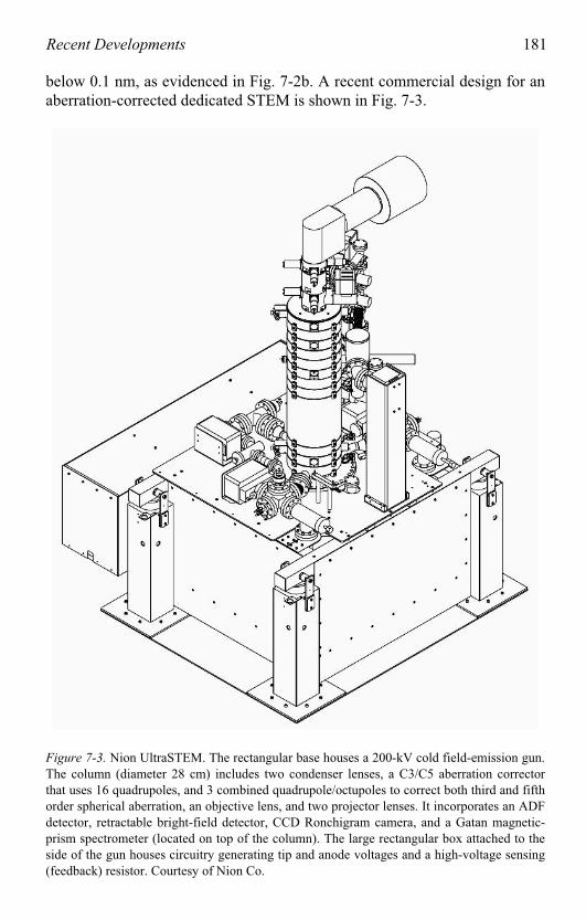
Recent Developments 181
below 0.1 nm, as evidenced in Fig. 7-2b. A recent commercial design for anaberration-corrected dedicated STEM is shown in Fig. 7-3.
Figure 7-3. Nion UltraSTEM. The rectangular base houses a 200-kV cold field-emission gun. The column (diameter 28 cm) includes two condenser lenses, a C3/C5 aberration correctorthat uses 16 quadrupoles, and 3 combined quadrupole/octupoles to correct both third and fifthorder spherical aberration, an objective lens, and two projector lenses. It incorporates an ADF detector, retractable bright-field detector, CCD Ronchigram camera, and a Gatan magnetic-prism spectrometer (located on top of the column). The large rectangular box attached to the side of the gun houses circuitry generating tip and anode voltages and a high-voltage sensing(feedback) resistor. Courtesy of Nion Co.
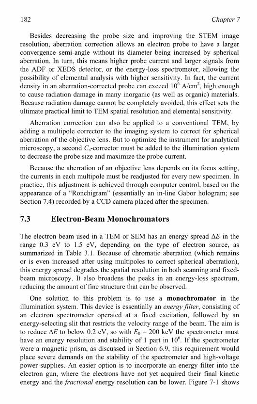
182 Chapter 7
Besides decreasing the probe size and improving the STEM imageresolution, aberration correction allows an electron probe to have a larger convergence semi-angle without its diameter being increased by sphericalaberration. In turn, this means higher probe current and larger signals fromthe ADF or XEDS detector, or the energy-loss spectrometer, allowing the possibility of elemental analysis with higher sensitivity. In fact, the current density in an aberration-corrected probe can exceed 106 A/cm2, high enoughto cause radiation damage in many inorganic (as well as organic) materials.Because radiation damage cannot be completely avoided, this effect sets the ltimate practical limit to TEM spatial resolution and elemental sensitivity.u
Aberration correction can also be applied to a conventional TEM, byadding a multipole corrector to the imaging system to correct for sphericalaberration of the objective lens. But to optimize the instrument for analyticalmicroscopy, a second Cs-corrector must be added to the illumination systemo decrease the probe size and maximize the probe current. t
Because the aberration of an objective lens depends on its focus setting, the currents in each multipole must be readjusted for every new specimen. In practice, this adjustment is achieved through computer control, based on theappearance of a “Ronchigram” (essentially an in-line Gabor hologram; seeSection 7.4) recorded by a CCD camera placed after the specimen.
7.3 Electron-Beam Monochromators
The electron beam used in a TEM or SEM has an energy spread E in the range 0.3 eV to 1.5 eV, depending on the type of electron source, assummarized in Table 3.1. Because of chromatic aberration (which remains or is even increased after using multipoles to correct spherical aberration), this energy spread degrades the spatial resolution in both scanning and fixed-beam microscopy. It also broadens the peaks in an energy-loss spectrum,reducing the amount of fine structure that can be observed.
One solution to this problem is to use a monochromator in theillumination system. This device is essentially an energy filter, consisting ofan electron spectrometer operated at a fixed excitation, followed by anenergy-selecting slit that restricts the velocity range of the beam. The aim isto reduce E to below 0.2 eV, so with E0 = 200 keV the spectrometer musthave an energy resolution and stability of 1 part in 106. If the spectrometerwere a magnetic prism, as discussed in Section 6.9, this requirement would place severe demands on the stability of the spectrometer and high-voltagepower supplies. An easier option is to incorporate an energy filter into the electron gun, where the electrons have not yet acquired their final kinetic energy and the fractional energy resolution can be lower. Figure 7-1 shows
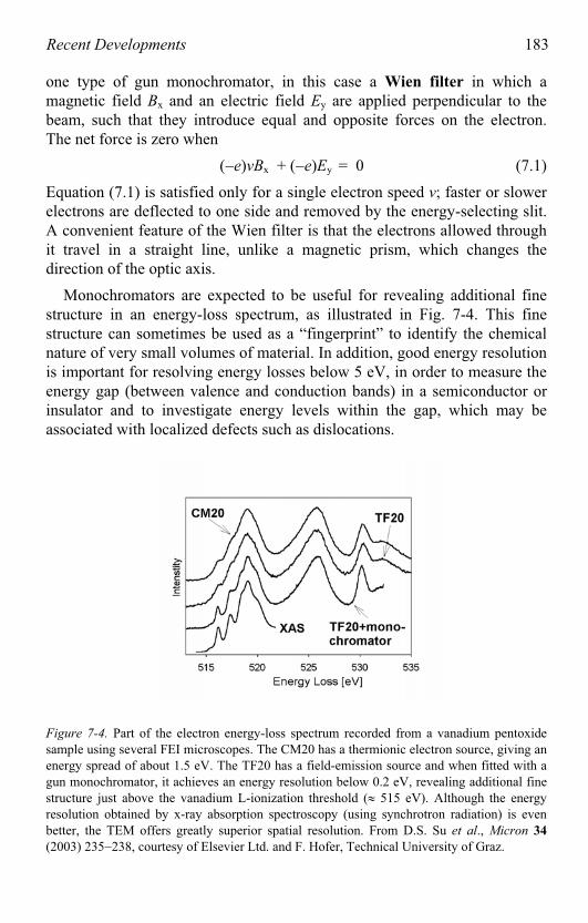
Recent Developments 183
one type of gun monochromator, in this case a Wien filter in which amagnetic field Bx and an electric field Ey are applied perpendicular to the beam, such that they introduce equal and opposite forces on the electron. The net force is zero when
( e)vBx + ( e)Ey = 0 (7.1)
Equation (7.1) is satisfied only for a single electron speed v; faster or slower electrons are deflected to one side and removed by the energy-selecting slit. A convenient feature of the Wien filter is that the electrons allowed through it travel in a straight line, unlike a magnetic prism, which changes the direction of the optic axis.
Monochromators are expected to be useful for revealing additional fine structure in an energy-loss spectrum, as illustrated in Fig. 7-4. This fine structure can sometimes be used as a “fingerprint” to identify the chemicalnature of very small volumes of material. In addition, good energy resolutionis important for resolving energy losses below 5 eV, in order to measure theenergy gap (between valence and conduction bands) in a semiconductor orinsulator and to investigate energy levels within the gap, which may be associated with localized defects such as dislocations.
Figure 7-4. Part of the electron energy-loss spectrum recorded from a vanadium pentoxidesample using several FEI microscopes. The CM20 has a thermionic electron source, giving anenergy spread of about 1.5 eV. The TF20 has a field-emission source and when fitted with a gun monochromator, it achieves an energy resolution below 0.2 eV, revealing additional finestructure just above the vanadium L-ionization threshold ( 515 eV). Although the energyresolution obtained by x-ray absorption spectroscopy (using synchrotron radiation) is evenbetter, the TEM offers greatly superior spatial resolution. From D.S. Su et al., Micron 34
(2003) 235 238, courtesy of Elsevier Ltd. and F. Hofer, Technical University of Graz.
184 Chapter 7
7.4 Electron Holography
Although the behavior of electrons can often be understood by treating themas particles, some properties, such as the distribution of intensity within an electron-diffraction pattern, require a wave description. But when an imageor diffraction pattern is viewed (on a fluorescent screen) or photographed(using a film or CCD camera), only the intensity (or amplitude) of the electron wave is recorded; we lose all information about the phase of the wave that arrives at the recording plane. As we will see, this phase carries additional information about the electric and magnetic fields that may be present in the specimen.
In holographic recording, electron or light waves coming from a sampleare mixed with a reference wave. The resulting interference pattern (called a hologram) is sensitive to the phase of the wave at the exit surface of the
specimen. So even though it is recorded only as an intensity distribution, thehologram contains both amplitude and phase information, which can be extracted by means of a reconstruction procedure. This procedure involvesinterference between the holographic record and a reconstruction wave, not necessarily of the original wavelength or even the same type of radiation.
L 1
z
Z
O S
specimen
L 2
hologram
electron
lens
Figure 7-5. In-line electron hologram formed from spherical waves emanating from a smallsource O (formed by an electron lens L1), which interfere with spherical waves emitted fromscattering points (such as S) in the specimen. For reconstruction, a light-optical lens L2
focuses light onto the back (or front) of the hologram, which then focuses the transmitted (or reflected) light onto each point S, forming a magnified image of the specimen.
Recent Developments 185
Besides having the same wavelength, the reference wave must have a fixed phase relationship with the wave that travels through the specimen.One means of achieving this is to have both waves originate from a small(ideally point) source, a distance z from the specimen; see Fig 7-5. Thissource can be produced by using a strong electron lens L1 to focus an electron beam into a small probe, as first proposed by Gabor (1948). If the specimen is very thin, some electrons are transmitted straight through thespecimen and interfere with those that are scattered within it. Interference between transmitted and scattered waves produces a hologram on a nearby screen or photographic plate.
This hologram has some of the features of a shadow image, a projectionof the specimen with magnification M z/ z. However, each scattering point S in the specimen emits spherical waves (similar to those centered on S in Fig. 7-5) that interfere with the spherical waves coming from the pointsource, so the hologram is also an interference pattern. For example, bright fringes are formed when there is constructive interference (where wavefrontsof maximum amplitude coincide at the hologram plane). In the case of athree-dimensional specimen, scattering points S occur at different z-coordinates, and their relative displacements (along the z-axis) have an effecton the interference pattern. As a result, the hologram can record three-
dimensional information, as its name is meant to suggest (holo = entire).
Reconstruction can be accomplished by using visible light of wavelengthM , which reaches the hologram through the glass lens L2 in Fig. 7-5. The interference fringes recorded in the hologram act rather like a zone plate (ora diffraction grating), directing the light into a magnified image of the specimen at S, as indicated by the dashed rays in Fig. 7-5. Because M may be large (e.g., 105), this reconstruction is best done in a separate apparatus. If the defects (aberrations, astigmatism) of the glass lens L2 match those of the electron lens L1, the electron-lens defects are compensated, and so theresolution in the reconstructed image is not limited by those aberrations.
At the time when Gabor made his proposal, no suitable electron source was available; he demonstrated the holographic principle using only visiblelight. Nowadays, light-optical holography has been made into a practicaltechnique by the development of laser sources of highly monochromaticradiation (small spread in wavelength, also described as high longitudinal
coherence). In electron optics, a monochromatic source is one that emitselectrons of closely the same kinetic energy (low energy spread E). Inaddition, the electron source should have a very small diameter (giving highlateral coherence). As a result, the widespread use of electron holographyhad to await the commercial availability of the field-emission TEM.
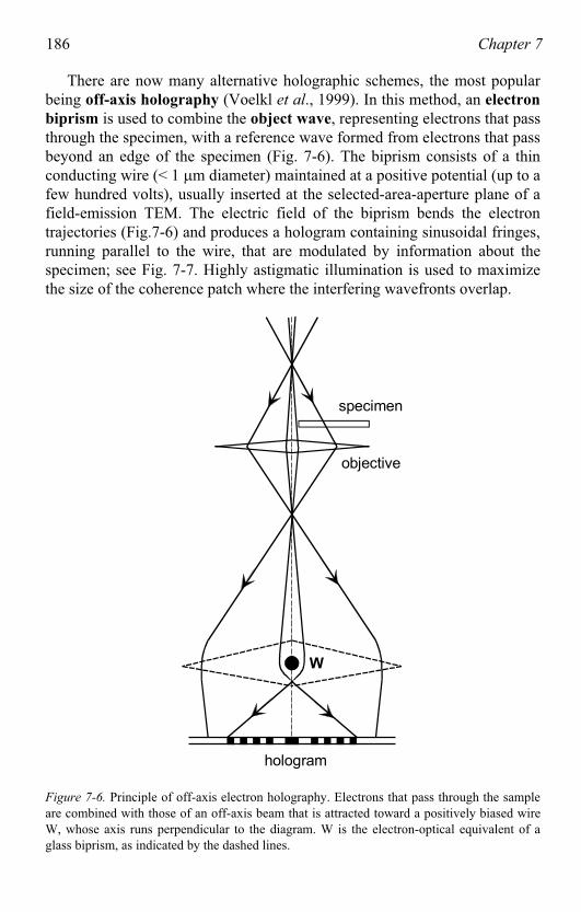
186 Chapter 7
There are now many alternative holographic schemes, the most popular being off-axis holography (Voelkl et al., 1999). In this method, an electron
biprism is used to combine the object wave, representing electrons that pass through the specimen, with a reference wave formed from electrons that pass beyond an edge of the specimen (Fig. 7-6). The biprism consists of a thinconducting wire (< 1 m diameter) maintained at a positive potential (up to afew hundred volts), usually inserted at the selected-area-aperture plane of a field-emission TEM. The electric field of the biprism bends the electrontrajectories (Fig.7-6) and produces a hologram containing sinusoidal fringes, running parallel to the wire, that are modulated by information about thespecimen; see Fig. 7-7. Highly astigmatic illumination is used to maximizethe size of the coherence patch where the interfering wavefronts overlap.
specimen
objective
hologram
W
Figure 7-6. Principle of off-axis electron holography. Electrons that pass through the sample are combined with those of an off-axis beam that is attracted toward a positively biased wireW, whose axis runs perpendicular to the diagram. W is the electron-optical equivalent of a glass biprism, as indicated by the dashed lines.
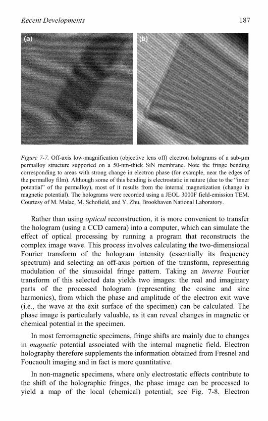
Recent Developments 187
Figure 7-7. Off-axis low-magnification (objective lens off) electron holograms of a sub- mpermalloy structure supported on a 50-nm-thick SiN membrane. Note the fringe bendingcorresponding to areas with strong change in electron phase (for example, near the edges ofthe permalloy film). Although some of this bending is electrostatic in nature (due to the “innerpotential” of the permalloy), most of it results from the internal magnetization (change in magnetic potential). The holograms were recorded using a JEOL 3000F field-emission TEM. Courtesy of M. Malac, M. Schofield, and Y. Zhu, Brookhaven National Laboratory.
Rather than using optical reconstruction, it is more convenient to transferthe hologram (using a CCD camera) into a computer, which can simulate theeffect of optical processing by running a program that reconstructs the complex image wave. This process involves calculating the two-dimensionalFourier transform of the hologram intensity (essentially its frequencyspectrum) and selecting an off-axis portion of the transform, representingmodulation of the sinusoidal fringe pattern. Taking an inverse Fouriertransform of this selected data yields two images: the real and imaginaryparts of the processed hologram (representing the cosine and sineharmonics), from which the phase and amplitude of the electron exit wave (i.e., the wave at the exit surface of the specimen) can be calculated. Thephase image is particularly valuable, as it can reveal changes in magnetic or che ical potential in the specimen.m
In most ferromagnetic specimens, fringe shifts are mainly due to changesin magnetic potential associated with the internal magnetic field. Electron holography therefore supplements the information obtained from Fresnel andFoucaoult imaging and in fact is more quantitative.
In non-magnetic specimens, where only electrostatic effects contribute tothe shift of the holographic fringes, the phase image can be processed to yield a map of the local (chemical) potential; see Fig. 7-8. Electron
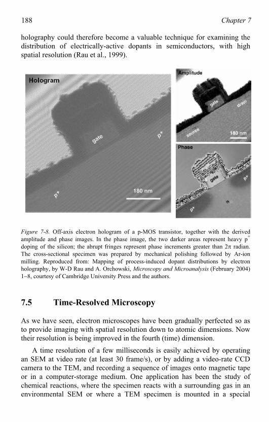
188 Chapter 7
holography could therefore become a valuable technique for examining the distribution of electrically-active dopants in semiconductors, with highspatial resolution (Rau et al., 1999).
Figure 7-8. Off-axis electron hologram of a p-MOS transistor, together with the derivedamplitude and phase images. In the phase image, the two darker areas represent heavy p
+
doping of the silicon; the abrupt fringes represent phase increments greater than 2 radian. The cross-sectional specimen was prepared by mechanical polishing followed by Ar-ionmilling. Reproduced from: Mapping of process-induced dopant distributions by electronholography, by W-D Rau and A. Orchowski, Microscopy and Microanalysis (February 2004)1 8, courtesy of Cambridge University Press and the authors.
7.5 Time-Resolved Microscopy
As we have seen, electron microscopes have been gradually perfected so as to provide imaging with spatial resolution down to atomic dimensions. Now their resolution is being improved in the fourth (time) dimension.
A time resolution of a few milliseconds is easily achieved by operatingan SEM at video rate (at least 30 frame/s), or by adding a video-rate CCDcamera to the TEM, and recording a sequence of images onto magnetic tape or in a computer-storage medium. One application has been the study of chemical reactions, where the specimen reacts with a surrounding gas in an environmental SEM or where a TEM specimen is mounted in a special
Recent Developments 189
holder containing an environmental cell. To allow adequate gas pressureinside, the latter employs small differential-pumping apertures or very thincarbon-film “windows” above and below the specimen.
Recent efforts have shortened the time resolution to the sub-picosecond region. One example (Lobastov et al., 2005) is a 120-keV TEM fitted with a lanthanum hexaboride cathode from which electrons are released, not bythermionic emission but via the photoelectric effect. The LaB6 is illuminatedby the focused beam from an ultrafast laser that produces short pulses of UVlight, repeated at intervals of 13 ns and each less than 100 femtoseconds long (1 fs = 10-15 s). The result is a pulsed electron beam, similar to that used for stroboscopic imaging in the SEM (see page 141) but with much shorter pulses. As the electron is a charged particle, incorporating many of them intothe same pulse would result in significant Coulomb repulsion between the electrons so that they no longer travel independently, as needed to focus them with electromagnetic lenses. This problem is circumvented by reducingthe laser-light intensity, so that each pulse generates (on average) only oneelectron. Although the laser pulses themselves can be used for ultrafastimaging, the image resolution is then limited by the photon wavelength.
One goal of such ultrafast microscopy is to study the atomic-scaledynamics of chemical reactions; it is known that the motion of individualatoms in a molecular structure occurs on a femtosecond time scale. Another aim is to obtain structural information from beam-sensitive (e.g., biological)specimens before they become damaged by the electron beam (Neutze et al.,2000).
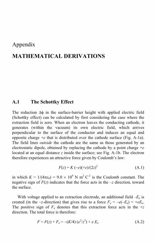
Appendix
MATHEMATICAL DERIVATIONS
A.1 The Schottky Effect
The reduction in the surface-barrier height with applied electric field (Schottky effect) can be calculated by first considering the case where the extraction field is zero. When an electron leaves the conducting cathode, it generates (within the vacuum) its own electric field, which arrives perpendicular to the surface of the conductor and induces an equal and opposite charge +e that is distributed over the cathode surface (Fig. A-1a). The field lines outside the cathode are the same as those generated by anelectrostatic dipole, obtained by replacing the cathode by a point charge +e
located at an equal distance z inside the surface; see Fig. A-1b. The electrontherefore experiences an attractive force given by Coulomb’s law:
F(z) = K ( e)(+e)/(2z)2 (A.1)
in which K = 1/(4 0) = 9.0 109 N m2 C-2 is the Coulomb constant. The negative sign of F(z) indicates that the force acts in the –z direction, toward the surface.
With voltage applied to an extraction electrode, an additional field –Ee iscreated (in the –z-direction) that gives rise to a force Fe = –e(–Ee) = +eEe.The positive sign of Fe denotes that this extraction force acts in the +z
direction. The total force is therefore:
F = F(z) + Fe = (K/4) (e2/z2) + e Ee (A.2)
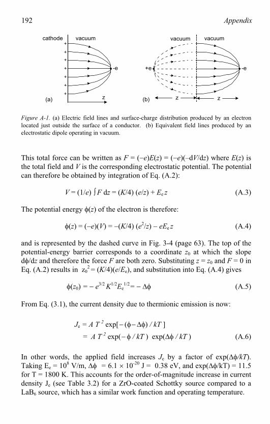
192 Appendix
-e+e
vacuum vacuum
zz
-e
cathode vacuum
z
+
+
+
+
+
+
+
(a) (b)
Figure A-1. (a) Electric field lines and surface-charge distribution produced by an electronlocated just outside the surface of a conductor. (b) Equivalent field lines produced by anelectrostatic dipole operating in vacuum.
This total force can be written as F = ( e)E(z) = ( e)(–dV/dz) where E(z) is the total field and V is the corresponding electrostatic potential. The potentialcan therefore be obtained by integration of Eq. (A.2):
V = (1/e) F dz = (K/4) (e/z) + Ee z (A.3)
The potential energy (z) of the electron is therefore:
(z) = ( e)(V) = (K/4) (e2/z) eEe z (A.4)
and is represented by the dashed curve in Fig. 3-4 (page 63). The top of the potential-energy barrier corresponds to a coordinate z0 at which the sloped /dz and therefore the force F are both zero. Substituting z = z0 and F = 0 in Eq. (A.2) results in z0
2 = (K/4)(e/Ee), and substitution into Eq. (A.4) gives
(z0) = e3/2 K1/2Ee1/2= (A.5)
From Eq. (3.1), the current density due to thermionic emission is now:
Je = A T 2 exp[ ( ) / kT ]
= A T 2 exp( / kT ) exp( / kT ) (A.6)
In other words, the applied field increases Je by a factor of exp( /kT).Taking Ee = 108 V/m, = 6.1 10-20 J = 0.38 eV, and exp( /kT) = 11.5for T = 1800 K. This accounts for the order-of-magnitude increase in currentdensity Je (see Table 3.2) for a ZrO-coated Schottky source compared to aLaB6 source, which has a similar work function and operating temperature.
Mathematical Derivations 193
A.2 Impact Parameter in Rutherford Scattering
Here we retrace Rutherford’s derivation of the relation between the impactparameter b and the scattering angle , but replacing his incident alpha particle by an electron and assuming that the scattering angle is small (true for most electrons, if their incident kinetic energy is high). Figure A-2 shows the hyperbolic path of an electron deflected by the electrostatic field of an unscreened atomic nucleus. At any instant, the electron is attracted toward the nucleus with an electrostatic force given by Eq. (4.10):
F = K Ze2/r2 (A.7)
where K = 1/(4 0) as previously. During the electron trajectory, this forcevaries in both magnitude and direction; its net effect must be obtained byintegrating over the path of the electron.
However, only the x-component Fx of the force is responsible for angulardeflection and this component is
Fx = F cos = (KZe2/r2) cos (A.8)
E
ABN
b
V1
Vx
V0
Vz
r
x
z
Figure A-2. Trajectory of an electron E with an impact parameter b relative to an unscreenedatomic nucleus N, whose electrostatic field causes the electron to be deflected through anangle , with a slight change in speed from v0 to v1 .
194 Appendix
The variable represents the direction of the force, relative to the x-axis(Fig. A-2). From the geometry of triangle ANE, we have: r cos = AN b if
is small, where b is the impact parameter of the initial trajectory.Substituting for r in Eq. (A.8) gives:
(KZe2/b2)cos3 = Fx = m(dvx/dt) (A.9)
where m = m0 is the relativistic mass of the electron, and we have appliedNewton's second law of motion in the x-direction. The final x-component vx
of electron velocity (resulting from the deflection) is obtained by integratingEq. (A.9) with respect to time, over the whole trajectory, as follows:
vx = (dvx/dt) dt = [(dvx/dt)/(dz/dt)] dz
= [(dvx/dt)/vz] (dz/d ) d (A.10)
In Eq. (A.10), we first replace integration over time by integration over the z-coordinate of the electron, and then by integration over the angle .Because z = (EN) tan b tan , basic calculus gives dz/d b(sec2 ).Using this relationship in Eq. (A.10) and making use of Eq. (A.9) tosubstitute for dvx/dt , vx can be written entirely in terms of as the only variable:
vx = [(Fx/m)/vz] b(sec2 ) d = [KZe2/(bmvz) cos3 ] sec2 d (A.11)
From the vector triangle in Fig. A-2 we have: vz = v1 cos v1 for small and also, for small , v1 v0, as elastic scattering causes only a very smallractional change in kinetic energy of the electron. Because sec = 1/cos ,f
vx = [KZe2/(bmv0)] cos d = [KZe2/(bmv0)] [sin ]
= 2 [KZe2/(bmv0)] (A.12)
where we have taken the limits of integration to be = /2 (electron farfrom the nucleus and approaching it) and = + /2 (electron far from the ucleus and receding from it).n
Finally, we obtain the scattering angle from parallelogram (or triangle) of velocity vectors in Fig. A-2, using the fact that tan = vx/vz vx/v0 to give:
2KZe2/(bmv02) = 2KZe2/( m0v0
2b) (A.13)
Using a non-relativistic approximation for the kinetic energy of the electron (E0 mv2/2), Eq. (A.13) becomes:
K Z e2 /(E0 b) (A.14)
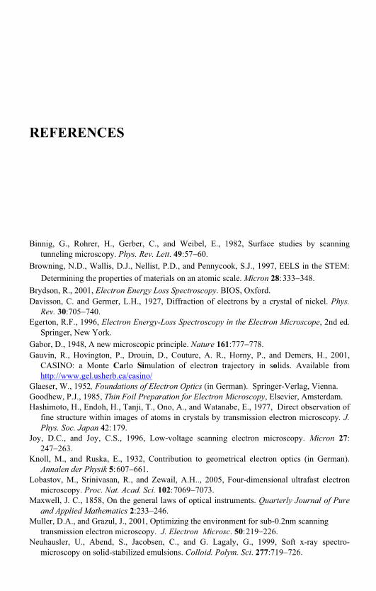
REFERENCES
Binnig, G., Rohrer, H., Gerber, C., and Weibel, E., 1982, Surface studies by scanningtunneling microscopy. Phys. Rev. Lett. 49:57 60.
Browning, N.D., Wallis, D.J., Nellist, P.D., and Pennycook, S.J., 1997, EELS in the STEM:
Determining the properties of materials on an atomic scale. Micron 28:333 348.
Brydson, R., 2001, Electron Energy Loss Spectroscopy. BIOS, Oxford.Davisson, C. and Germer, L.H., 1927, Diffraction of electrons by a crystal of nickel. Phys.
Rev. 30:705 740.Egerton, R.F., 1996, Electron Energy-Loss Spectroscopy in the Electron Microscope, 2nd ed.
Springer, New York.
Gabor, D., 1948, A new microscopic principle. Nature 161:777 778.Gauvin, R., Hovington, P., Drouin, D., Couture, A. R., Horny, P., and Demers, H., 2001,
CASINO: a Monte Carlo Simulation of electron trajectory in solids. Available fromhttp://www.gel.usherb.ca/casino/
Glaeser, W., 1952, Foundations of Electron Optics (in German). Springer-Verlag, Vienna.Goodhew, P.J., 1985, Thin Foil Preparation for Electron Microscopy, Elsevier, Amsterdam.Hashimoto, H., Endoh, H., Tanji, T., Ono, A., and Watanabe, E., 1977, Direct observation of
fine structure within images of atoms in crystals by transmission electron microscopy. J.
Phys. Soc. Japan 42:179.Joy, D.C., and Joy, C.S., 1996, Low-voltage scanning electron microscopy. Micron 27:
247 263.Knoll, M., and Ruska, E., 1932, Contribution to geometrical electron optics (in German).
Annalen der Physik 5:607 661.Lobastov, M., Srinivasan, R., and Zewail, A.H.., 2005, Four-dimensional ultrafast electron
microscopy. Proc. Nat. Acad. Sci. 102:7069 7073.Maxwell, J. C., 1858, On the general laws of optical instruments. Quarterly Journal of Pure
and Applied Mathematics 2:233 246.Muller, D.A., and Grazul, J., 2001, Optimizing the environment for sub-0.2nm scanning
transmission electron microscopy. J. Electron Microsc. 50:219 226.Neuhausler, U., Abend, S., Jacobsen, C., and G. Lagaly, G., 1999, Soft x-ray spectro-
microscopy on solid-stabilized emulsions. Colloid. Polym. Sci. 277:719 726.
196 References
Neutze, R., Wouts, R., van der Spoel, D., Weckert, E., and Hajdu, J., 2000, Potential forbiomolecular imaging with femtosecond X-ray pulses. Nature 406:752 757.
Rau, W.D., Schwander, P., Baumann, F.H., Hoeppner, W., and Ourmadz, A., 1999, Two-dimensional mapping of the electrostatic potential in transistors by electron holography.Phys. Rev. Lett. 82:2614 2617.
Reimer, L., 1997, Transmission Electron Microscopy, 4th edition, Springer-Verlag, Berlin.Reimer, L , 1998, Scanning Electron Microscopy, 2nd edition. Springer-Verlag, Heidelberg.Rempfer, G.F., Delage, D.N., Skoczlas, W.P. and Griffith, O.H., 1997, Simultaneous
correction of spherical and chromatic aberrations with an electron mirror: an opticalachromat. Microscopy and Microanalysis 3:14 27.
Shindo, D., and Oikawa, T., 2002, Analytical Electron Microscopy for Materials Science.Springer, London.
Thomson, G.P., 1927, Diffraction of cathode rays by thin films of platinum. Nature 120:802.Voekl, E., Allard, L.F., and Joy, D.C., 1999, Introduction to Electron Holography. Springer,
New York.Williams, D.B., and Carter, C.B., 1996, Transmission Electron Microscopy, Springer, New
York.Zhang, H., 2002, Transmission electron microscopy for the semiconductor industry. Micron
33:517 525.
Zwyorkin, V.K., Hillier, J. and Snyder, R.L., 1942, A scanning electron microscope. ASTM
Bull. 117:15.
INDEX
Aberrations, 3, 28axial, 44 chromatic, 33, 48 correction of, 180 spherical, 33, 44
Acceleration of electrons, 67 AEM, 21, 155Astigmatism, 51, 145Atomic-force microscope, 24Airlock, 76 Alignment,
of multipoles, 180 of TEM, 12, 40, 75
Amorphous specimens, 100 Analytical microscopy, 155 Anode plate, 67 Aperture,
condenser, 72of the eye, 3 pressure-differential, 149 selected-area, 83 SEM objective, 147 TEM objective, 80
Areal density, 98, 166Artifacts of image 23, 24, 148
Astigmatism,axial, 51 SEM, 145 TEM condenser, 74 TEM objective, 82, 116
Atom,Bohr model, 155 Rutherford model, 93
Auger electron, 166, 171Autobias, 61 Axial symmetry, 34, 36 Azimuthal angle, 51, 34, 177
Back-focal plane, 32, 80 Backscattering, 129, 17 Backstreaming, 92 Bend contour, 114 Biological TEM, 79 Biological tissue, 102, 76, 15Biprism, 185Bloch waves, 115 Boersch effect, 67 Bohr radius, 155Bragg reflection, 106Bremsstrahlung x-rays, 20
198 Index
Bright-field image, 100 Brightness, 65
conservation of, 66, 72
Camera length, 110Cathode material, 60 Cathode-ray tube, 34, 127Cathodoluminescence, 134 CCD camera, 86 Charging effects, 147 Cleavage, 120 Coefficient,
backscattering, 137 chromatic, 51 spherical-aberration, 45
Coherence, 185 Coma, 54 Condenser aperture, 74, 72Condenser lenses, 70 Condenser-objective lens, 79 Contamination, 92, 82, 152Confusion,
Airy disk of, 4aberration disk, 33, 47, 49 disk of least, 46 focusing disk of, 28
Contrast,atomic-number, 101diffraction, 106light-microscope, 6 mass-thickness, 101 phase, 115 scattering, 101, 80 thickness-gradient, 104 topographical, 131 148
Convergence angle, 66, 72Cornea, 2 Coulomb interaction, 93 Cross section for scattering, 97 Crossover, 71Curvature of field, 29, 55
Dedicated STEM, 19, 177Depth of field,
in TEM, 88, 55in SEM, 145, 18
Depth of focus,in TEM, 87
Defects,crystal, 14, 112, 122, 141lens, 27, 30, 44, 185
Detector,ADF, 177Everhart-Thornley, 135in-lens, 136Robinson, 138solid-state, 138x-ray, 161, 168, 9
Diaphragm,of the eye, 3 TEM condenser, 72 TEM objective, 80
Diffraction,light-optical, 3electron, 106, 11
Diffraction contrast, 108 Diffraction pattern, 108 Dark-field image, 108 Dead time, 164Disk of confusion, 4, 28, 33Disk of least confusion, 46Dislocations, 14, 112, 183Dispersion,
electron, 172photon, 33, 142, 161, 168
Distortion, 28, 54 Drift,
beam-current, 61high-voltage, 70, 43, 49illumination, 75 specimen, 75, 77, 78STM, 24
Dynamics of scattering, 97
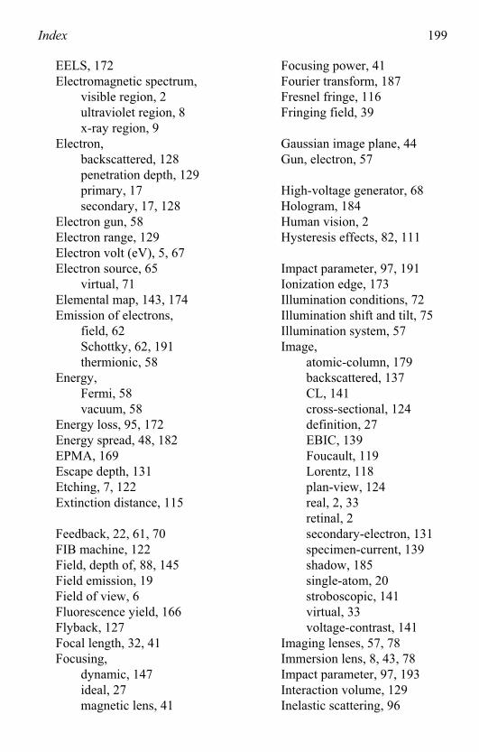
Index 199
EELS, 172 Electromagnetic spectrum,
visible region, 2 ultraviolet region, 8x-ray region, 9
Electron,backscattered, 128penetration depth, 129primary, 17secondary, 17, 128
Electron gun, 58 Electron range, 129 Electron volt (eV), 5, 67 Electron source, 65
virtual, 71Elemental map, 143, 174Emission of electrons,
field, 62Schottky, 62, 191 thermionic, 58
Energy,Fermi, 58vacuum, 58
Energy loss, 95, 172Energy spread, 48, 182 EPMA, 169 Escape depth, 131 Etching, 7, 122Extinction distance, 115
Feedback, 22, 61, 70FIB machine, 122Field, depth of, 88, 145Field emission, 19 Field of view, 6 Fluorescence yield, 166Flyback, 127 Focal length, 32, 41Focusing,
dynamic, 147ideal, 27 magnetic lens, 41
Focusing power, 41 Fourier transform, 187 Fresnel fringe, 116 Fringing field, 39
Gaussian image plane, 44 Gun, electron, 57
High-voltage generator, 68Hologram, 184 Human vision, 2 Hysteresis effects, 82, 111
Impact parameter, 97, 191Ionization edge, 173 Illumination conditions, 72 Illumination shift and tilt, 75Illumination system, 57 Image,
atomic-column, 179backscattered, 137CL, 141 cross-sectional, 124definition, 27EBIC, 139 Foucault, 119 Lorentz, 118 plan-view, 124real, 2, 33 retinal, 2 secondary-electron, 131specimen-current, 139 shadow, 185 single-atom, 20 stroboscopic, 141 virtual, 33 voltage-contrast, 141
Imaging lenses, 57, 78 Immersion lens, 8, 43, 78Impact parameter, 97, 193Interaction volume, 129 Inelastic scattering, 96
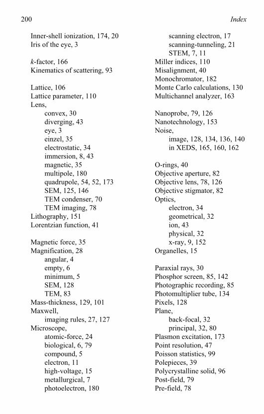
200 Index
Inner-shell ionization, 174, 20 Iris of the eye, 3
k-factor, 166 Kinematics of scattering, 93
Lattice, 106 Lattice parameter, 110 Lens,
convex, 30diverging, 43eye, 3 einzel, 35 electrostatic, 34 immersion, 8, 43 magnetic, 35 multipole, 180 quadrupole, 54, 52, 173SEM, 125, 146TEM condenser, 70 TEM imaging, 78
Lithography, 151 Lorentzian function, 41
Magnetic force, 35 Magnification, 28
angular, 4 empty, 6minimum, 5SEM, 128TEM, 83
Mass-thickness, 129, 101 Maxwell,
imaging rules, 27, 127Microscope,
atomic-force, 24biological, 6, 79compound, 5electron, 11 high-voltage, 15metallurgical, 7photoelectron, 180
scanning electron, 17scanning-tunneling, 21STEM, 7, 11
Miller indices, 110 Misalignment, 40 Monochromator, 182Monte Carlo calculations, 130 Multichannel analyzer, 163
Nanoprobe, 79, 126Nanotechnology, 153 Noise,
image, 128, 134, 136, 140in XEDS, 165, 160, 162
O-rings, 40 Objective aperture, 82 Objective lens, 78, 126Objective stigmator, 82 Optics,
electron, 34 geometrical, 32 ion, 43physical, 32 x-ray, 9, 152
Organelles, 15
Paraxial rays, 30 Phosphor screen, 85, 142Photographic recording, 85Photomultiplier tube, 134 Pixels, 128 Plane,
back-focal, 32 principal, 32, 80
Plasmon excitation, 173Point resolution, 47 Poisson statistics, 99 Polepieces, 39 Polycrystalline solid, 96 Post-field, 79 Pre-field, 78
Index 201
Principal plane, 32, 80Probe,
electron, 17, 126scanning, 21
Prismglass, 30 magnetic, 172
Pulse-height analysis, 163Pump,
cryo, 91 diffusion, 89 ion, 90rotary, 88 turbomolecular, 90
Pupil of the eye, 3
Quantum number, 155 Quadrupole, 52, 54, 173
Raster scanning, 17, 126Radiation damage, 151, 182Ray diagram, 32, 34Rayleigh criterion, 4, 81Refractive index, 8, 30Relativistic mass, 68Replica, 103 Resist, 151 Resistor,
bias, 61, 70feedback, 69
Resolution,of eye, 5of light microscope, 6 of retina, 4 of SEM, 144, 125, 126of TEM, 82, 180, 182
Richardson law, 59 Ripple, 43, 49, 69 Ronchigram, 182 Rotation angle of image, 42 Rutherford scattering, 93, 193Rydberg energy, 155
Saturated filament, 62 Scanning,
digital, 127raster, 126, 17
Scattering, 93angular distribution, 97 cross section, 97 elastic, 96 inelastic, 96, 49
Scattering contrast, 80 Scintillator, 134 Secondary electrons, 17 Screen,
SEM display, 128 TEM viewing, 85
Screening, 99SEM, 17, 125
environmental, 149 low-voltage, 149
SE1 component, 143Shadowing, 104, 136Single scattering, 99Spatial resolution,
of the retina, 4of the eye, 5 of a light microscope, 6
Specimen,amorphous, 100cross-sectional, 124insulating, 148polycrystalline, 96single-crystal, 112TEM thickness, 101, 88
Specimen preparation, SEM, 147 TEM, 119
Specimen stage, 75, 57Spectroscopy,
Auger, 171 energy-loss, 172 x-ray, 161, 168
Staining, 6, 15, 101
202 Index
Stacking fault, 114 Stage,
side-entry, 76top-entry, 77
STEM, 18, 177Steradian, 65 Stigmator, 52
condenser, 74objective, 82, 145 SEM, 145
STM, 21 Surface replica, 103 Symmetry, axial, 34 39Symmetry, crystal, 112 Synchrotron source, 10
TEM,history, 11construction, 57
Thickness fringes, 114 Thickness measurement, 174Thin-film deposition, 122Thin-lens approximation, 32 Thinning of specimens, 121 Topographic contrast,
in SEM, 131 in STM, 22
Tunneling, 21, 63
Ultrafast microscopy, 188Ultramicrotome, 101, 120Unit cell, 110 Units of length, 1
Vacancy clusters, 114 Vacuum system, 88 Viewing screen, 85
Water window, 10Wavelength,
of electrons, 11, 117of light, 2
Wehnelt electrode, 61 Wien filter, 183 Work function, 58 Working distance, 143
X-ray,bremsstrahlung, 160characteristic, 158
X-ray microscope, 9 X-ray spectroscopy, 158, 143XEDS, 161 XWDS, 168
Y-modulation, 25 Yield,
backscattering, 137fluorescence, 166secondary-electron, 131total-electron, 148
Z-contrast, 101ZAF correction, 167Zero-loss peak, 173Zone plate, 9, 152