Embed Size (px)
Citation preview
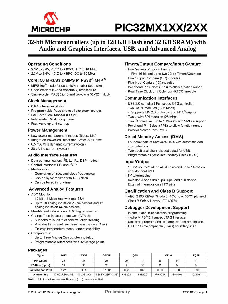
PIC32MX1XX/2XX32-bit Microcontrollers (up to 128 KB Flash and 32 KB SRAM) with
Audio and Graphics Interfaces, USB, and Advanced Analog
Operating Conditions• 2.3V to 3.6V, -40ºC to +105ºC, DC to 40 MHz• 2.3V to 3.6V, -40ºC to +85ºC, DC to 50 MHz
Core: 50 MHz/83 DMIPS MIPS32® M4K®
• MIPS16e® mode for up to 40% smaller code size• Code-efficient (C and Assembly) architecture• Single-cycle (MAC) 32x16 and two-cycle 32x32 multiply
Clock Management• 0.9% internal oscillator• Programmable PLLs and oscillator clock sources• Fail-Safe Clock Monitor (FSCM)• Independent Watchdog Timer• Fast wake-up and start-up
Power Management• Low-power management modes (Sleep, Idle)• Integrated Power-on Reset and Brown-out Reset• 0.5 mA/MHz dynamic current (typical)• 20 μA IPD current (typical)
Audio Interface Features• Data communication: I2S, LJ, RJ, DSP modes• Control interface: SPI and I2C™• Master clock:
- Generation of fractional clock frequencies- Can be synchronized with USB clock- Can be tuned in run-time
Advanced Analog Features• ADC Module:
- 10-bit 1.1 Msps rate with one S&H- Up to 10 analog inputs on 28-pin devices and 13
analog inputs on 44-pin devices• Flexible and independent ADC trigger sources• Charge Time Measurement Unit (CTMU):
- Supports mTouch™ capacitive touch sensing- Provides high-resolution time measurement (1 ns)- On-chip temperature measurement capability
• Comparators:- Up to three Analog Comparator modules- Programmable references with 32 voltage points
Timers/Output Compare/Input Capture• Five General Purpose Timers:
- Five 16-bit and up to two 32-bit Timers/Counters• Five Output Compare (OC) modules• Five Input Capture (IC) modules• Peripheral Pin Select (PPS) to allow function remap• Real-Time Clock and Calendar (RTCC) module
Communication Interfaces• USB 2.0-compliant Full-speed OTG controller• Two UART modules (12.5 Mbps)
- Supports LIN 2.0 protocols and IrDA® support• Two 4-wire SPI modules (25 Mbps)• Two I2C modules (up to 1 Mbaud) with SMBus support• Peripheral Pin Select (PPS) to allow function remap• Parallel Master Port (PMP)
Direct Memory Access (DMA)• Four channels of hardware DMA with automatic data
size detection• Two additional channels dedicated for USB• Programmable Cyclic Redundancy Check (CRC)
Input/Output• 10 mA source/sink on all I/O pins and up to 14 mA on
non-standard VOH
• 5V-tolerant pins• Selectable open drain, pull-ups, and pull-downs• External interrupts on all I/O pins
Qualification and Class B Support• AEC-Q100 REVG (Grade 2 -40ºC to +105ºC) planned• Class B Safety Library, IEC 60730
Debugger Development Support• In-circuit and in-application programming• 4-wire MIPS® Enhanced JTAG interface• Unlimited program and six complex data breakpoints• IEEE 1149.2-compatible (JTAG) boundary scan
PackagesType SOIC SSOP SPDIP QFN VTLA TQFP
Pin Count 28 28 28 28 44 36 44 44
I/O Pins (up to) 21 21 21 21 34 25 34 34
Contact/Lead Pitch 1.27 0.65 0.100'' 0.65 0.65 0.50 0.50 0.80
Dimensions 17.90x7.50x2.65 10.2x5.3x2 1.365''x.285''x.135'' 6x6x0.9 8x8x0.9 5x5x0.9 6x6x0.9 10x10x1
Note: All dimensions are in millimeters (mm) unless specified.
2011-2012 Microchip Technology Inc. Preliminary DS61168E-page 1
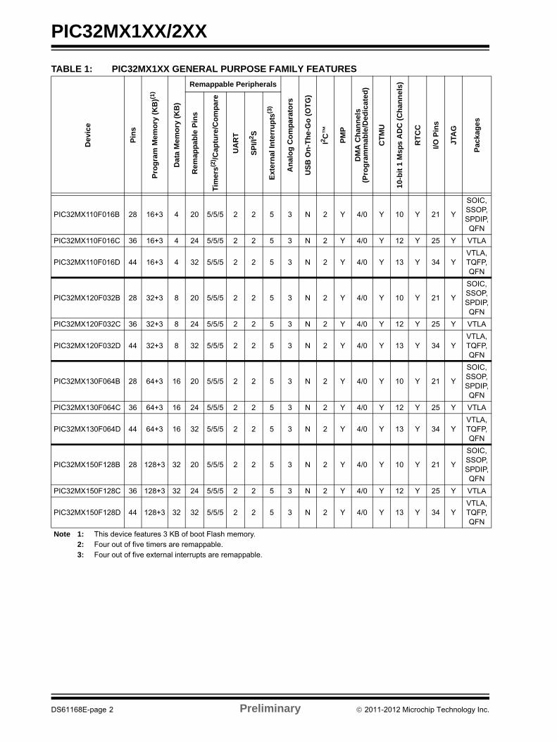
PIC32MX1XX/2XX
TABLE 1: PIC32MX1XX GENERAL PURPOSE FAMILY FEATURES
Dev
ice
Pin
s
Pro
gra
m M
emo
ry (
KB
)(1)
Dat
a M
emo
ry (
KB
)
Remappable Peripherals
An
alo
g C
om
par
ato
rs
US
B O
n-T
he-
Go
(O
TG
)
I2C
™
PM
P
DM
A C
han
nel
s(P
rog
ram
mab
le/D
edic
ated
)
CT
MU
10-
bit
1 M
sps
AD
C (
Ch
ann
els)
RT
CC
I/O P
ins
JTA
G
Pac
kag
es
Rem
app
able
Pin
s
Tim
ers(2
) /Cap
ture
/Co
mp
are
UA
RT
SP
I/I2 S
Ext
ern
al In
terr
up
ts(3
)
PIC32MX110F016B 28 16+3 4 20 5/5/5 2 2 5 3 N 2 Y 4/0 Y 10 Y 21 Y
SOIC, SSOP, SPDIP, QFN
PIC32MX110F016C 36 16+3 4 24 5/5/5 2 2 5 3 N 2 Y 4/0 Y 12 Y 25 Y VTLA
PIC32MX110F016D 44 16+3 4 32 5/5/5 2 2 5 3 N 2 Y 4/0 Y 13 Y 34 YVTLA, TQFP, QFN
PIC32MX120F032B 28 32+3 8 20 5/5/5 2 2 5 3 N 2 Y 4/0 Y 10 Y 21 Y
SOIC, SSOP, SPDIP, QFN
PIC32MX120F032C 36 32+3 8 24 5/5/5 2 2 5 3 N 2 Y 4/0 Y 12 Y 25 Y VTLA
PIC32MX120F032D 44 32+3 8 32 5/5/5 2 2 5 3 N 2 Y 4/0 Y 13 Y 34 YVTLA, TQFP, QFN
PIC32MX130F064B 28 64+3 16 20 5/5/5 2 2 5 3 N 2 Y 4/0 Y 10 Y 21 Y
SOIC, SSOP,SPDIP, QFN
PIC32MX130F064C 36 64+3 16 24 5/5/5 2 2 5 3 N 2 Y 4/0 Y 12 Y 25 Y VTLA
PIC32MX130F064D 44 64+3 16 32 5/5/5 2 2 5 3 N 2 Y 4/0 Y 13 Y 34 YVTLA, TQFP, QFN
PIC32MX150F128B 28 128+3 32 20 5/5/5 2 2 5 3 N 2 Y 4/0 Y 10 Y 21 Y
SOIC, SSOP,SPDIP, QFN
PIC32MX150F128C 36 128+3 32 24 5/5/5 2 2 5 3 N 2 Y 4/0 Y 12 Y 25 Y VTLA
PIC32MX150F128D 44 128+3 32 32 5/5/5 2 2 5 3 N 2 Y 4/0 Y 13 Y 34 YVTLA, TQFP, QFN
Note 1: This device features 3 KB of boot Flash memory.2: Four out of five timers are remappable.3: Four out of five external interrupts are remappable.
DS61168E-page 2 Preliminary 2011-2012 Microchip Technology Inc.
PIC32MX1XX/2XX
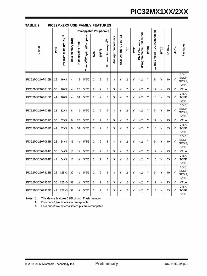
TABLE 2: PIC32MX2XX USB FAMILY FEATURES
Dev
ice
Pin
s
Pro
gra
m M
emo
ry (
KB
)(1)
Da
ta M
emo
ry (
KB
)
Remappable Peripherals
An
alo
g C
om
par
ato
rs
US
B O
n-T
he-
Go
(O
TG
)
I2 C™
PM
P
DM
A C
han
nel
s(P
rog
ram
mab
le/D
edic
ated
)
CT
MU
10-b
it 1
Msp
s A
DC
(C
han
nel
s)
RT
CC
I/O P
ins
JTA
G
Pac
kag
es
Rem
app
able
Pin
s
Tim
ers(2
) /Cap
ture
/Co
mp
are
UA
RT
SP
I/I2 S
Ext
ern
al In
terr
up
ts(3
)
PIC32MX210F016B 28 16+3 4 19 5/5/5 2 2 5 3 Y 2 Y 4/2 Y 9 Y 19 Y
SOIC, SSOP,SPDIP, QFN
PIC32MX210F016C 36 16+3 4 23 5/5/5 2 2 5 3 Y 2 Y 4/2 Y 12 Y 23 Y VTLA
PIC32MX210F016D 44 16+3 4 31 5/5/5 2 2 5 3 Y 2 Y 4/2 Y 13 Y 33 YVTLA, TQFP, QFN
PIC32MX220F032B 28 32+3 8 19 5/5/5 2 2 5 3 Y 2 Y 4/2 Y 9 Y 19 Y
SOIC, SSOP, SPDIP, QFN
PIC32MX220F032C 36 32+3 8 23 5/5/5 2 2 5 3 Y 2 Y 4/2 Y 12 Y 23 Y VTLA
PIC32MX220F032D 44 32+3 8 31 5/5/5 2 2 5 3 Y 2 Y 4/2 Y 13 Y 33 YVTLA, TQFP, QFN
PIC32MX230F064B 28 64+3 16 19 5/5/5 2 2 5 3 Y 2 Y 4/2 Y 9 Y 19 Y
SOIC, SSOP, SPDIP, QFN
PIC32MX230F064C 36 64+3 16 23 5/5/5 2 2 5 3 Y 2 Y 4/2 Y 12 Y 23 Y VTLA
PIC32MX230F064D 44 64+3 16 31 5/5/5 2 2 5 3 Y 2 Y 4/2 Y 13 Y 33 YVTLA, TQFP, QFN
PIC32MX250F128B 28 128+3 32 19 5/5/5 2 2 5 3 Y 2 Y 4/2 Y 9 Y 19 Y
SOIC, SSOP, SPDIP, QFN
PIC32MX250F128C 36 128+3 32 23 5/5/5 2 2 5 3 Y 2 Y 4/2 Y 12 Y 23 Y VTLA
PIC32MX250F128D 44 128+3 32 31 5/5/5 2 2 5 3 Y 2 Y 4/2 Y 13 Y 33 YVTLA, TQFP, QFN
Note 1: This device features 3 KB of boot Flash memory.2: Four out of five timers are remappable.3: Four out of five external interrupts are remappable.
2011-2012 Microchip Technology Inc. Preliminary DS61168E-page 3
PIC32MX1XX/2XX
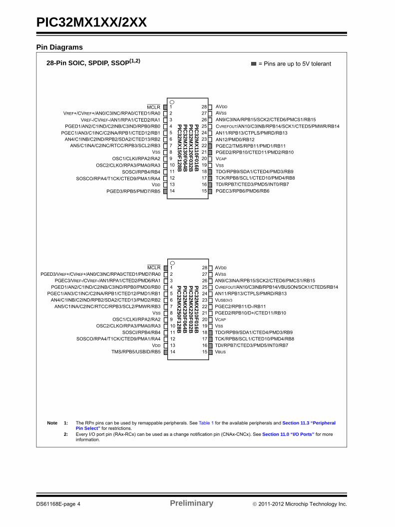
Pin Diagrams
Note 1: The RPn pins can be used by remappable peripherals. See Table 1 for the available peripherals and Section 11.3 “Peripheral Pin Select” for restrictions.
2: Every I/O port pin (RAx-RCx) can be used as a change notification pin (CNAx-CNCx). See Section 11.0 “I/O Ports” for more information.
VREF+/CVREF+/AN0/C3INC/RPA0/CTED1/RA0
VREF-/CVREF-/AN1/RPA1/CTED2/RA1 AN9/C3INA/RPB15/SCK2/CTED6/PMCS1/RB15
PGED1/AN2/C1IND/C2INB/C3IND/RPB0/RB0 CVREFOUT/AN10/C3INB/RPB14/SCK1/CTED5/PMWR/RB14
PGEC1/AN3/C1INC/C2INA/RPB1/CTED12/RB1 AN11/RPB13/CTPLS/PMRD/RB13AN4/C1INB/C2IND/RPB2/SDA2/CTED13/RB2 AN12/PMD0/RB12
PGEC2/TMS/RPB11/PMD1/RB11VSS PGED2/RPB10/CTED11/PMD2/RB10
OSC1/CLKI/RPA2/RA2
OSC2/CLKO/RPA3/PMA0/RA3 VSS
SOSCI/RPB4/RB4 TDO/RPB9/SDA1/CTED4/PMD3/RB9
SOSCO/RPA4/T1CK/CTED9/PMA1/RA4 TCK/RPB8/SCL1/CTED10/PMD4/RB8
VDD TDI/RPB7/CTED3/PMD5/INT0/RB7
PGEC3/RPB6/PMD6/RB6
AVDD
AVSS
AN5/C1INA/C2INC/RTCC/RPB3/SCL2/RB3
28-Pin SOIC, SPDIP, SSOP(1,2) = Pins are up to 5V tolerant
MCLR
VCAP
PGED3/RPB5/PMD7/RB5
MCLR 1 28 AVDD
PGED3/VREF+/CVREF+/AN0/C3INC/RPA0/CTED1/PMD7/RA0 2 27 AVSS
PGEC3/VREF-/CVREF-/AN1/RPA1/CTED2/PMD6/RA1 3 26 AN9/C3INA/RPB15/SCK2/CTED6/PMCS1/RB15
PGED1/AN2/C1IND/C2INB/C3IND/RPB0/PMD0/RB0 4 25 CVREFOUT/AN10/C3INB/RPB14/VBUSON/SCK1/CTED5/RB14PGEC1/AN3/C1INC/C2INA/RPB1/CTED12/PMD1/RB1 5 24 AN11/RPB13/CTPLS/PMRD/RB13
AN4/C1INB/C2IND/RPB2/SDA2/CTED13/PMD2/RB2 6 23 VUSB3V3
AN5/C1INA/C2INC/RTCC/RPB3/SCL2/PMWR/RB3 7 22 PGEC2/RPB11/D-/RB11
VSS 8 21 PGED2/RPB10/D+/CTED11/RB10
OSC1/CLKI/RPA2/RA2 9 20 VCAP
OSC2/CLKO/RPA3/PMA0/RA3 10 19 VSS
SOSCI/RPB4/RB4 11 18 TDO/RPB9/SDA1/CTED4/PMD3/RB9
SOSCO/RPA4/T1CK/CTED9/PMA1/RA4 12 17 TCK/RPB8/SCL1/CTED10/PMD4/RB8
VDD 13 16 TDI/RPB7/CTED3/PMD5/INT0/RB7TMS/RPB5/USBID/RB5 14 15 VBUS
PIC
32MX
210F016B
PIC
32MX
220F032B
1 28
2 27
3 26
4 25
5 24
6 23
7 22
8 21
9 20
10 19
11 18
12 17
13 16
14 15
PIC
32MX
110F016B
PIC
32MX
120F032B
PIC
32MX
130F064B
PIC
32MX
150F128B
PIC
32MX
230F064B
PIC
32MX
250F128B
DS61168E-page 4 Preliminary 2011-2012 Microchip Technology Inc.
PIC32MX1XX/2XX
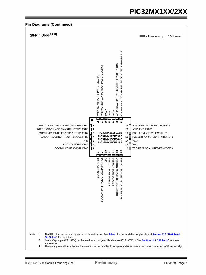
Pin Diagrams (Continued)
28-Pin QFN(1,2,3)= Pins are up to 5V tolerant
Note 1: The RPn pins can be used by remappable peripherals. See Table 1 for the available peripherals and Section 11.3 “Peripheral Pin Select” for restrictions.
2: Every I/O port pin (RAx-RCx) can be used as a change notification pin (CNAx-CNCx). See Section 11.0 “I/O Ports” for more information.
3: The metal plane at the bottom of the device is not connected to any pins and is recommended to be connected to VSS externally.
VR
EF-/
CV
RE
F-/
AN
1/R
PA
1/C
TE
D2
/RA
1
VR
EF+
/CV
RE
F+
/AN
0/C
3IN
C/R
PA
0/C
TE
D1/
RA
0
MC
LR
AV
DD
AV
SS
AN
9/C
3IN
A/R
PB
15
/SC
K2
/CT
ED
6/P
MC
S1
/RB
15
CV
RE
FO
UT/A
N10
/C3I
NB
/RP
B1
4/S
CK
1/C
TE
D5
/PM
WR
/RB
14
28
27
26
25
24
23
22
PGED1/AN2/C1IND/C2INB/C3IND/RPB0/RB0 1 21 AN11/RPB13/CTPLS/PMRD/RB13
PGEC1/AN3/C1INC/C2INA/RPB1/CTED12/RB1 2 20 AN12/PMD0/RB12
AN4/C1INB/C2IND/RPB2/SDA2/CTED13/RB2 3 19 PGEC2/TMS/RPB11/PMD1/RB11
AN5/C1INA/C2INC/RTCC/RPB3/SCL2/RB3 4
PIC32MX110F016B
18 PGED2/RPB10/CTED11/PMD2/RB10
VSS 5 17 VCAP
OSC1/CLKI/RPA2/RA2 6 16 VSS
OSC2/CLKO/RPA3/PMA0/RA3 7 15 TDO/RPB9/SDA1/CTED4/PMD3/RB9
8 9 10
11
12
13
14
SO
SC
I/R
PB
4/R
B4
SO
SC
O/R
PA
4/T
1C
K/C
TE
D9
/PM
A1
/RA
4
VD
D
PG
ED
3/R
PB
5/P
MD
7/R
B5
PG
EC
3/R
PB
6/P
MD
6/R
B6
TD
I/R
PB
7/C
TE
D3/
PM
D5/
INT
0/R
B7
TC
K/R
PB
8/S
CL
1/C
TE
D10
/PM
D4
/RB
8
PIC32MX120F032BPIC32MX130F064BPIC32MX150F128B
2011-2012 Microchip Technology Inc. Preliminary DS61168E-page 5
PIC32MX1XX/2XX
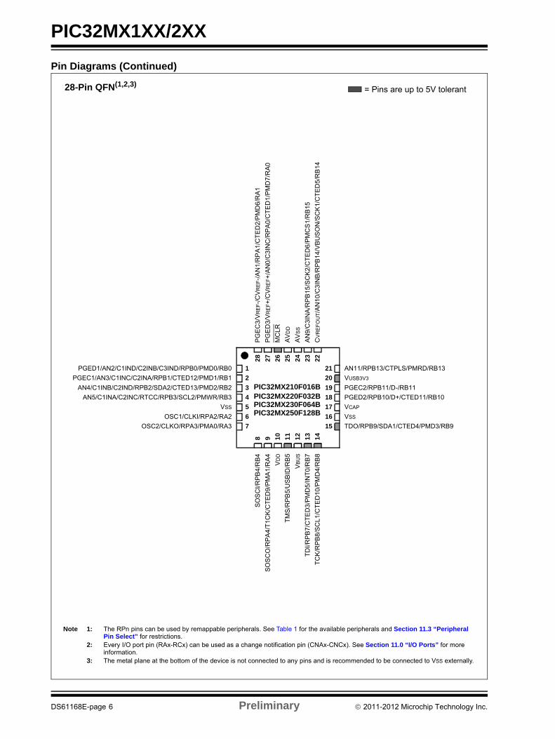
Pin Diagrams (Continued)
28-Pin QFN(1,2,3)= Pins are up to 5V tolerant
PG
EC
3/V
RE
F-/
CV
RE
F-/
AN
1/R
PA
1/C
TE
D2
/PM
D6
/RA
1
PG
ED
3/V
RE
F+
/CV
RE
F+
/AN
0/C
3IN
C/R
PA
0/C
TE
D1
/PM
D7
/RA
0
MC
LR
AV
DD
AV
SS
AN
9/C
3IN
A/R
PB
15
/SC
K2
/CT
ED
6/P
MC
S1/
RB
15
CV
RE
FO
UT/A
N1
0/C
3IN
B/R
PB
14/
VB
US
ON
/SC
K1/
CT
ED
5/R
B14
28
27
26
25
24
23
22
PGED1/AN2/C1IND/C2INB/C3IND/RPB0/PMD0/RB0 1 21 AN11/RPB13/CTPLS/PMRD/RB13
PGEC1/AN3/C1INC/C2INA/RPB1/CTED12/PMD1/RB1 2 20 VUSB3V3
AN4/C1INB/C2IND/RPB2/SDA2/CTED13/PMD2/RB2 3 19 PGEC2/RPB11/D-/RB11
AN5/C1INA/C2INC/RTCC/RPB3/SCL2/PMWR/RB3 4
PIC32MX210F016B18 PGED2/RPB10/D+/CTED11/RB10
VSS 5 17 VCAP
OSC1/CLKI/RPA2/RA2 6 16 VSS
OSC2/CLKO/RPA3/PMA0/RA3 7 15 TDO/RPB9/SDA1/CTED4/PMD3/RB9
8 9 10
11
12
13
14
SO
SC
I/R
PB
4/R
B4
SO
SC
O/R
PA
4/T
1C
K/C
TE
D9
/PM
A1
/RA
4
VD
D
TM
S/R
PB
5/U
SB
ID/R
B5
VB
US
TD
I/R
PB
7/C
TE
D3
/PM
D5
/IN
T0
/RB
7
TC
K/R
PB
8/S
CL
1/C
TE
D1
0/P
MD
4/R
B8
PIC32MX220F032B
Note 1: The RPn pins can be used by remappable peripherals. See Table 1 for the available peripherals and Section 11.3 “Peripheral Pin Select” for restrictions.
2: Every I/O port pin (RAx-RCx) can be used as a change notification pin (CNAx-CNCx). See Section 11.0 “I/O Ports” for more information.
3: The metal plane at the bottom of the device is not connected to any pins and is recommended to be connected to VSS externally.
PIC32MX230F064BPIC32MX250F128B
DS61168E-page 6 Preliminary 2011-2012 Microchip Technology Inc.
PIC32MX1XX/2XX
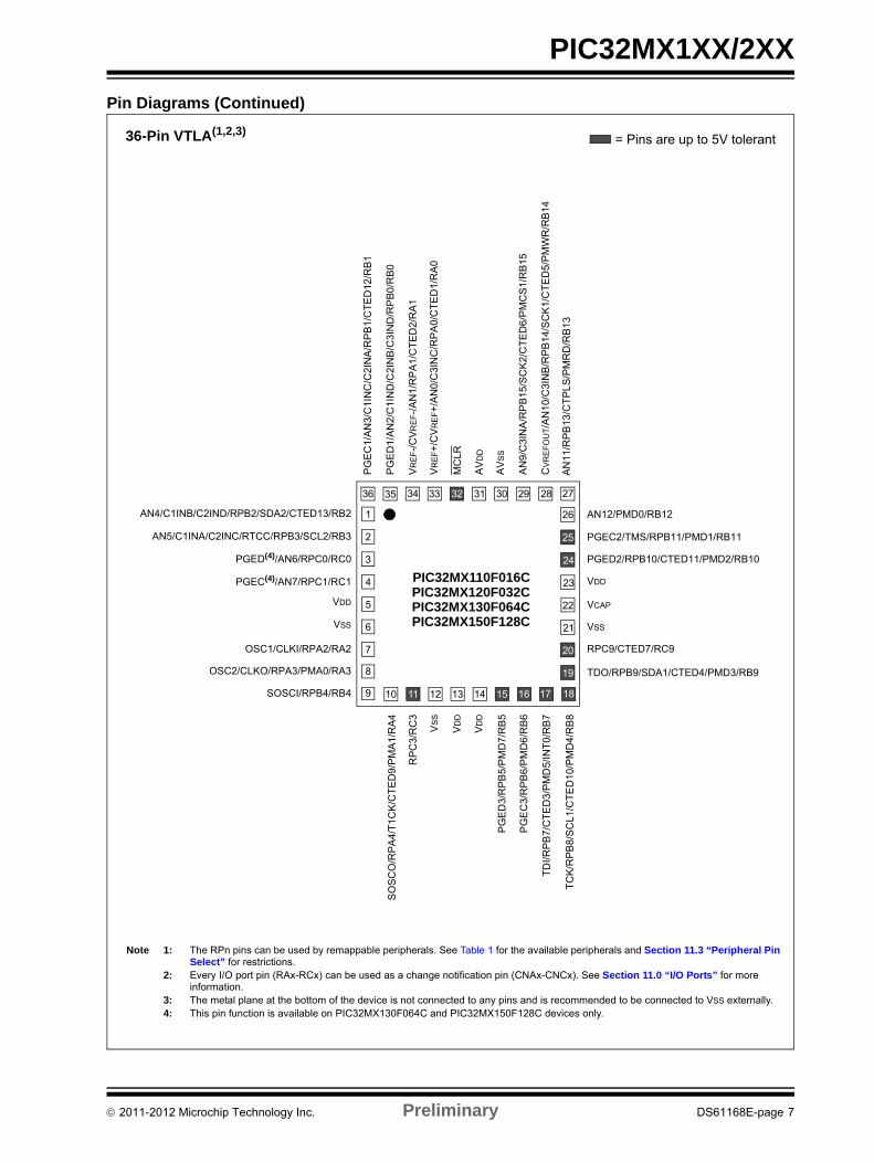
Pin Diagrams (Continued)
36-Pin VTLA(1,2,3)= Pins are up to 5V tolerant
Note 1: The RPn pins can be used by remappable peripherals. See Table 1 for the available peripherals and Section 11.3 “Peripheral Pin Select” for restrictions.
2: Every I/O port pin (RAx-RCx) can be used as a change notification pin (CNAx-CNCx). See Section 11.0 “I/O Ports” for more information.
3: The metal plane at the bottom of the device is not connected to any pins and is recommended to be connected to VSS externally.4: This pin function is available on PIC32MX130F064C and PIC32MX150F128C devices only.
PIC32MX120F032C
1
PIC32MX110F016C
10
33 32 31 30 29 28
2
3
4
5
6
24
23
22
21
20
19
11 12 13 14 15
7
8
9
343536
16 17 18
27
26
25
PG
EC
1/A
N3/
C1
INC
/C2I
NA
/RP
B1
/CT
ED
12/R
B1
PG
ED
1/A
N2/
C1
IND
/C2I
NB
/C3
IND
/RP
B0
/RB
0
VR
EF-/
CV
RE
F-/
AN
1/R
PA
1/C
TE
D2/
RA
1
VR
EF+
/CV
RE
F+
/AN
0/C
3IN
C/R
PA
0/C
TE
D1
/RA
0
MC
LR
AV
DD
AV
SS
AN
9/C
3IN
A/R
PB
15
/SC
K2/
CT
ED
6/P
MC
S1/
RB
15
CV
RE
FO
UT/A
N1
0/C
3IN
B/R
PB
14/
SC
K1
/CT
ED
5/P
MW
R/R
B1
4
AN4/C1INB/C2IND/RPB2/SDA2/CTED13/RB2
AN
11/R
PB
13/
CT
PL
S/P
MR
D/R
B1
3
AN5/C1INA/C2INC/RTCC/RPB3/SCL2/RB3
AN12/PMD0/RB12
PGED(4)/AN6/RPC0/RC0
PGEC2/TMS/RPB11/PMD1/RB11
PGEC(4)/AN7/RPC1/RC1
PGED2/RPB10/CTED11/PMD2/RB10
VDD
VDD
VSS
VCAP
OSC1/CLKI/RPA2/RA2
VSS
OSC2/CLKO/RPA3/PMA0/RA3
RPC9/CTED7/RC9
SOSCI/RPB4/RB4
TDO/RPB9/SDA1/CTED4/PMD3/RB9
SO
SC
O/R
PA
4/T
1C
K/C
TE
D9
/PM
A1
/RA
4
RP
C3
/RC
3
VS
S
VD
D
VD
D
PG
ED
3/R
PB
5/P
MD
7/R
B5
PG
EC
3/R
PB
6/P
MD
6/R
B6
TD
I/RP
B7
/CT
ED
3/P
MD
5/I
NT
0/R
B7
TC
K/R
PB
8/S
CL
1/C
TE
D1
0/P
MD
4/R
B8
PIC32MX130F064CPIC32MX150F128C
2011-2012 Microchip Technology Inc. Preliminary DS61168E-page 7
PIC32MX1XX/2XX
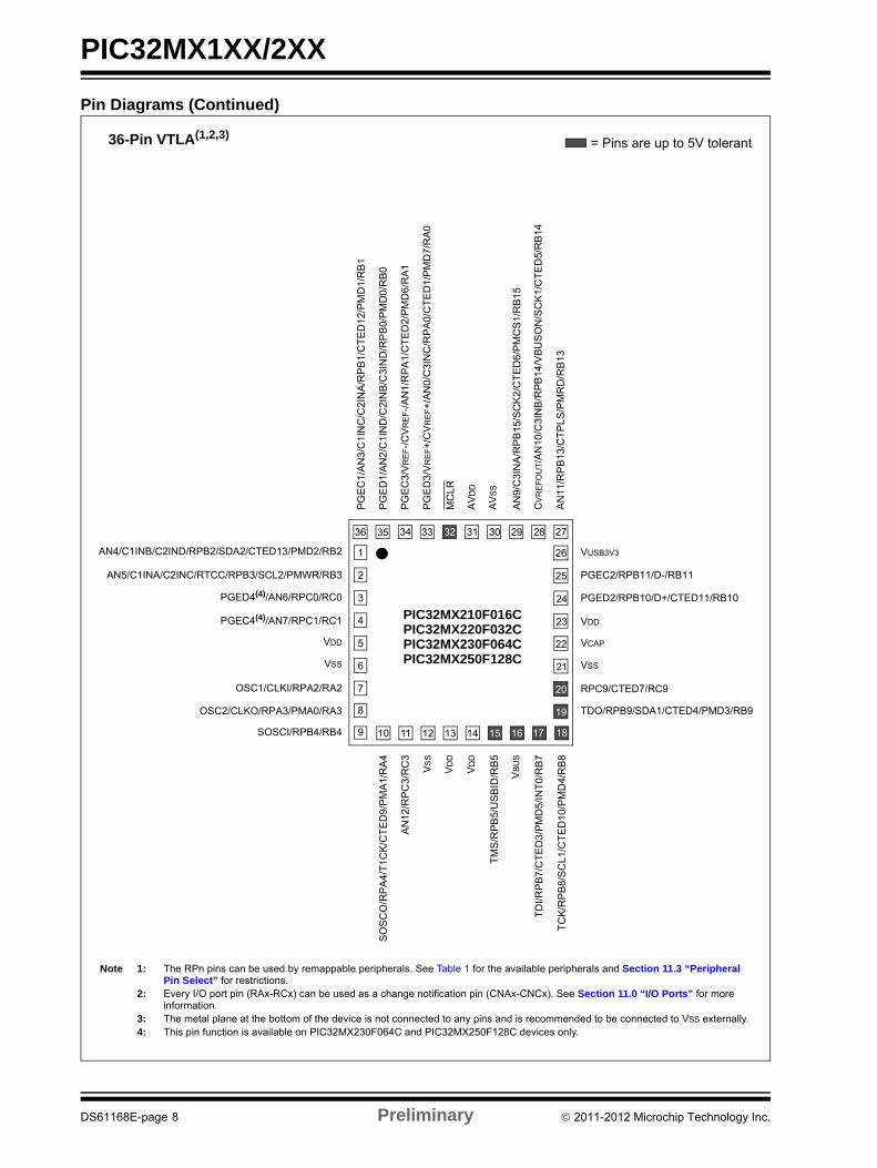
Pin Diagrams (Continued)
36-Pin VTLA(1,2,3)= Pins are up to 5V tolerant
Note 1: The RPn pins can be used by remappable peripherals. See Table 1 for the available peripherals and Section 11.3 “Peripheral Pin Select” for restrictions.
2: Every I/O port pin (RAx-RCx) can be used as a change notification pin (CNAx-CNCx). See Section 11.0 “I/O Ports” for more information.
3: The metal plane at the bottom of the device is not connected to any pins and is recommended to be connected to VSS externally.4: This pin function is available on PIC32MX230F064C and PIC32MX250F128C devices only.
PIC32MX220F032C
1
PIC32MX210F016C
10
33 32 31 30 29 28
2
3
4
5
6
24
23
22
21
20
19
11 12 13 14 15
7
8
9
343536
16 17 18
27
26
25
PG
EC
1/A
N3
/C1
INC
/C2
INA
/RP
B1/
CT
ED
12/
PM
D1/
RB
1
PG
ED
1/A
N2
/C1
IND
/C2
INB
/C3
IND
/RP
B0/
PM
D0
/RB
0
PG
EC
3/V
RE
F-/
CV
RE
F-/
AN
1/R
PA
1/C
TE
D2
/PM
D6
/RA
1
PG
ED
3/V
RE
F+
/CV
RE
F+
/AN
0/C
3IN
C/R
PA
0/C
TE
D1
/PM
D7
/RA
0
MC
LR
AV
DD
AV
SS
AN
9/C
3IN
A/R
PB
15/S
CK
2/C
TE
D6
/PM
CS
1/R
B1
5
CV
RE
FO
UT/A
N1
0/C
3IN
B/R
PB
14
/VB
US
ON
/SC
K1
/CT
ED
5/R
B1
4AN4/C1INB/C2IND/RPB2/SDA2/CTED13/PMD2/RB2
AN
11
/RP
B1
3/C
TP
LS
/PM
RD
/RB
13
AN5/C1INA/C2INC/RTCC/RPB3/SCL2/PMWR/RB3
VUSB3V3
PGED4(4)/AN6/RPC0/RC0
PGEC2/RPB11/D-/RB11
PGEC4(4)/AN7/RPC1/RC1
PGED2/RPB10/D+/CTED11/RB10
VDD
VCAP
OSC1/CLKI/RPA2/RA2
VSS
OSC2/CLKO/RPA3/PMA0/RA3
RPC9/CTED7/RC9
SOSCI/RPB4/RB4
TDO/RPB9/SDA1/CTED4/PMD3/RB9
SO
SC
O/R
PA
4/T
1C
K/C
TE
D9
/PM
A1
/RA
4
AN
12/R
PC
3/R
C3
VS
S
VD
D
VD
D
TM
S/R
PB
5/U
SB
ID/R
B5
VB
US
TD
I/R
PB
7/C
TE
D3/
PM
D5/
INT
0/R
B7
TC
K/R
PB
8/S
CL
1/C
TE
D1
0/P
MD
4/R
B8
VDD
VSS
PIC32MX230F064CPIC32MX250F128C
DS61168E-page 8 Preliminary 2011-2012 Microchip Technology Inc.
PIC32MX1XX/2XX
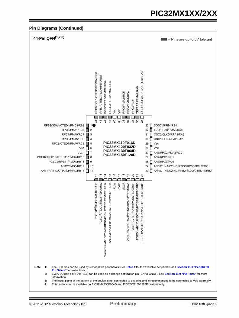
Pin Diagrams (Continued)
44-Pin QFN(1,2,3)= Pins are up to 5V tolerant
Note 1: The RPn pins can be used by remappable peripherals. See Table 1 for the available peripherals and Section 11.3 “Peripheral Pin Select” for restrictions.
2: Every I/O port pin (RAx-RCx) can be used as a change notification pin (CNAx-CNCx). See Section 11.0 “I/O Ports” for more information.
3: The metal plane at the bottom of the device is not connected to any pins and is recommended to be connected to VSS externally.4: This pin function is available on PIC32MX130F064D and PIC32MX150F128D devices only.
RP
B8/
SC
L1
/CT
ED
10
/PM
D4
/RB
8
RP
B7/
CT
ED
3/P
MD
5/IN
T0/
RB
7
PG
EC
3/R
PB
6/P
MD
6/R
B6
PG
ED
3/R
PB
5/P
MD
7/R
B5
VD
D
VS
S
RP
C5
/PM
A3/
RC
5
RP
C4
/PM
A4/
RC
4
RP
C3
/RC
3
TD
I/R
PA
9/P
MA
9/R
A9
SO
SC
O/R
PA
4/T
1C
K/C
TE
D9
/RA
4
44
43
42
41
40
39
38
37
36
35
34
RPB9/SDA1/CTED4/PMD3/RB9 1 33 SOSCI/RPB4/RB4
RPC6/PMA1/RC6 2 32 TDO/RPA8/PMA8/RA8
RPC7/PMA0/RC7 3 31 OSC2/CLKO/RPA3/RA3
RPC8/PMA5/RC8 4 30 OSC1/CLKI/RPA2/RA2
RPC9/CTED7/PMA6/RC9 5 29 VSS
VSS 6
PIC32MX110F016D
28 VDD
VCAP 7 27 AN8/RPC2/PMA2/RC2
PGED2/RPB10/CTED11/PMD2/RB10 8 26 AN7/RPC1/RC1
PGEC2/RPB11/PMD1/RB11 9 25 AN6/RPC0/RC0
AN12/PMD0/RB12 10 24 AN5/C1INA/C2INC/RTCC/RPB3/SCL2/RB3
AN11/RPB13/CTPLS/PMRD/RB13 11 23 AN4/C1INB/C2IND/RPB2/SDA2/CTED13/RB2
12
13
14
15
16
17
18
19
20
21
22
PG
ED
4(4
) /TM
S/P
MA
10
/RA
10
PG
EC
(4) /T
CK
/CT
ED
8/P
MA
7/R
A7
CV
RE
FO
UT/A
N1
0/C
3IN
B/R
PB
14
/SC
K1
/CT
ED
5/P
MW
R/R
B1
4
AN
9/C
3IN
A/R
PB
15/S
CK
2/C
TE
D6
/PM
CS
1/R
B1
5
AV
SS
AV
DD
MC
LR
VR
EF+
/CV
RE
F+
/AN
0/C
3IN
C/R
PA
0/C
TE
D1/
RA
0
VR
EF-/
CV
RE
F-/
AN
1/R
PA
1/C
TE
D2/
RA
1
PG
ED
1/A
N2
/C1
IND
/C2
INB
/C3
IND
/RP
B0/
RB
0
PG
EC
1/A
N3/
C1I
NC
/C2I
NA
/RP
B1/
CT
ED
12/
RB
1
PIC32MX120F032DPIC32MX130F064DPIC32MX150F128D
2011-2012 Microchip Technology Inc. Preliminary DS61168E-page 9
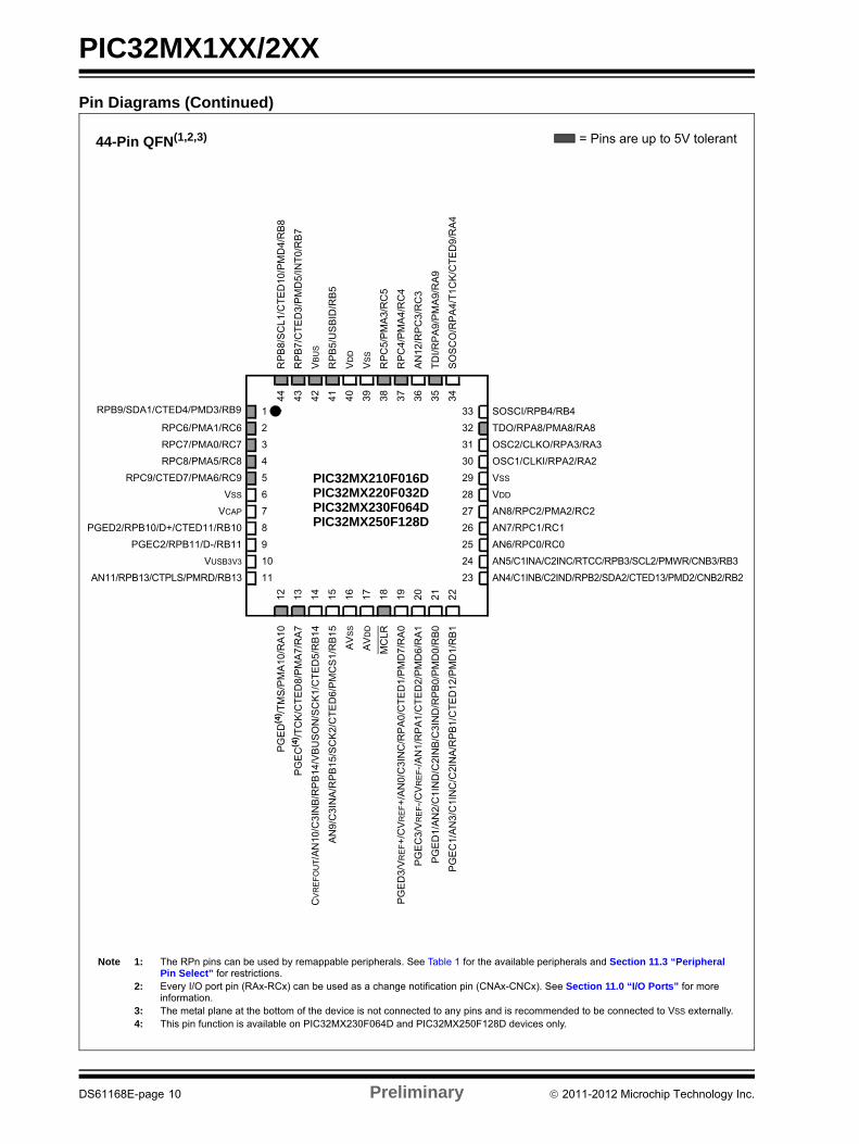
PIC32MX1XX/2XX
Pin Diagrams (Continued)
44-Pin QFN(1,2,3) = Pins are up to 5V tolerant
Note 1: The RPn pins can be used by remappable peripherals. See Table 1 for the available peripherals and Section 11.3 “Peripheral Pin Select” for restrictions.
2: Every I/O port pin (RAx-RCx) can be used as a change notification pin (CNAx-CNCx). See Section 11.0 “I/O Ports” for more information.
3: The metal plane at the bottom of the device is not connected to any pins and is recommended to be connected to VSS externally.4: This pin function is available on PIC32MX230F064D and PIC32MX250F128D devices only.
RP
B8
/SC
L1/
CT
ED
10/
PM
D4/
RB
8
RP
B7
/CT
ED
3/P
MD
5/I
NT
0/R
B7
VB
US
RP
B5
/US
BID
/RB
5
VD
D
VS
S
RP
C5
/PM
A3
/RC
5
RP
C4
/PM
A4
/RC
4
AN
12
/RP
C3
/RC
3
TD
I/RP
A9
/PM
A9/
RA
9
SO
SC
O/R
PA
4/T
1C
K/C
TE
D9
/RA
4
44
43
42
41
40
39
38
37
36
35
34
1 33 SOSCI/RPB4/RB4
RPC6/PMA1/RC6 2 32 TDO/RPA8/PMA8/RA8
RPC7/PMA0/RC7 3 31 OSC2/CLKO/RPA3/RA3
RPC8/PMA5/RC8 4 30 OSC1/CLKI/RPA2/RA2
RPC9/CTED7/PMA6/RC9 5 29 VSS
VSS 6
PIC32MX210F016D28 VDD
VCAP 7 27 AN8/RPC2/PMA2/RC2
8 26 AN7/RPC1/RC1
PGEC2/RPB11/D-/RB11 9 25 AN6/RPC0/RC0
VUSB3V3 10 24 AN5/C1INA/C2INC/RTCC/RPB3/SCL2/PMWR/CNB3/RB3
AN11/RPB13/CTPLS/PMRD/RB13 11 23 AN4/C1INB/C2IND/RPB2/SDA2/CTED13/PMD2/CNB2/RB2
12
13
14
15
16
17
18
19
20
21
22
PG
ED
(4) /T
MS
/PM
A10
/RA
10
PG
EC
(4) /T
CK
/CT
ED
8/P
MA
7/R
A7
CV
RE
FO
UT/A
N1
0/C
3IN
B/R
PB
14/V
BU
SO
N/S
CK
1/C
TE
D5
/RB
14
AN
9/C
3IN
A/R
PB
15
/SC
K2/
CT
ED
6/P
MC
S1
/RB
15
AV
SS
AV
DD
MC
LR
PG
ED
3/V
RE
F+
/CV
RE
F+
/AN
0/C
3IN
C/R
PA
0/C
TE
D1
/PM
D7
/RA
0
PG
EC
3/V
RE
F-/
CV
RE
F-/
AN
1/R
PA
1/C
TE
D2
/PM
D6
/RA
1
PG
ED
1/A
N2/
C1
IND
/C2I
NB
/C3
IND
/RP
B0
/PM
D0
/RB
0
PG
EC
1/A
N3
/C1I
NC
/C2I
NA
/RP
B1
/CT
ED
12/P
MD
1/R
B1
PGED2/RPB10/D+/CTED11/RB10
RPB9/SDA1/CTED4/PMD3/RB9
PIC32MX220F032DPIC32MX230F064DPIC32MX250F128D
DS61168E-page 10 Preliminary 2011-2012 Microchip Technology Inc.

PIC32MX1XX/2XX
Pin Diagrams (Continued)
44-Pin TQFP(1,2,3)= Pins are up to 5V tolerant
Note 1: The RPn pins can be used by remappable peripherals. See Table 1 for the available peripherals and Section 11.3 “Peripheral Pin Select” for restrictions.
2: Every I/O port pin (RAx-RCx) can be used as a change notification pin (CNAx-CNCx). See Section 11.0 “I/O Ports” for more information.
3: The metal plane at the bottom of the device is not connected to any pins and is recommended to be connected to VSS externally.4: This pin function is available on PIC32MX130F064D and PIC32MX150F128D devices only.
RP
B8/
SC
L1
/CT
ED
10
/PM
D4
/RB
8
RP
B7/
CT
ED
3/P
MD
5/IN
T0/
RB
7
PG
EC
3/R
PB
6/P
MD
6/R
B6
PG
ED
3/R
PB
5/P
MD
7/R
B5
VD
D
VS
S
RP
C5
/PM
A3/
RC
5
RP
C4
/PM
A4/
RC
4
RP
C3
/RC
3
TD
I/R
PA
9/P
MA
9/R
A9
SO
SC
O/R
PA
4/T
1C
K/C
TE
D9
/RA
4
44
43
42
41
40
39
38
37
36
35
34
RPB9/SDA1/CTED4/PMD3/RB9 1 33 SOSCI/RPB4/RB4
RPC6/PMA1/RC6 2 32 TDO/RPA8/PMA8/RA8
RPC7/PMA0/RC7 3 31 OSC2/CLKO/RPA3/RA3
RPC8/PMA5/RC8 4 30 OSC1/CLKI/RPA2/RA2
RPC9/CTED7/PMA6/RC9 5 29 VSS
VSS 6
PIC32MX110F016D28 VDD
VCAP 7 27 AN8/RPC2/PMA2/RC2
PGED2/RPB10/CTED11/PMD2/RB10 8 26 AN7/RPC1/RC1
PGEC2/RPB11/PMD1/RB11 9 25 AN6/RPC0/RC0
AN12/PMD0/RB12 10 24 AN5/C1INA/C2INC/RTCC/RPB3/SCL2/RB3
AN11/RPB13/CTPLS/PMRD/RB13 11 23 AN4/C1INB/C2IND/RPB2/SDA2/CTED13/RB2
12
13
14
15
16
17
18
19
20
21
22
PG
ED
(4) /T
MS
/PM
A10
/RA
10
PG
EC
(4) /T
CK
/CT
ED
8/P
MA
7/R
A7
CV
RE
FO
UT/A
N1
0/C
3IN
B/R
PB
14/S
CK
1/C
TE
D5
/PM
WR
/RB
14
AN
9/C
3IN
A/R
PB
15
/SC
K2
/CT
ED
6/P
MC
S1
/RB
15
AV
SS
AV
DD
MC
LR
VR
EF+
/CV
RE
F+
/AN
0/C
3IN
C/R
PA
0/C
TE
D1
/RA
0
VR
EF-/
CV
RE
F-/
AN
1/R
PA
1/C
TE
D2
/RA
1
PG
ED
1/A
N2
/C1I
ND
/C2
INB
/C3
IND
/RP
B0
/RB
0
PG
EC
1/A
N3
/C1
INC
/C2
INA
/RP
B1
/CT
ED
12
/RB
1
PIC32MX120F032DPIC32MX130F064DPIC32MX150F128D
2011-2012 Microchip Technology Inc. Preliminary DS61168E-page 11
PIC32MX1XX/2XX
Pin Diagrams (Continued)
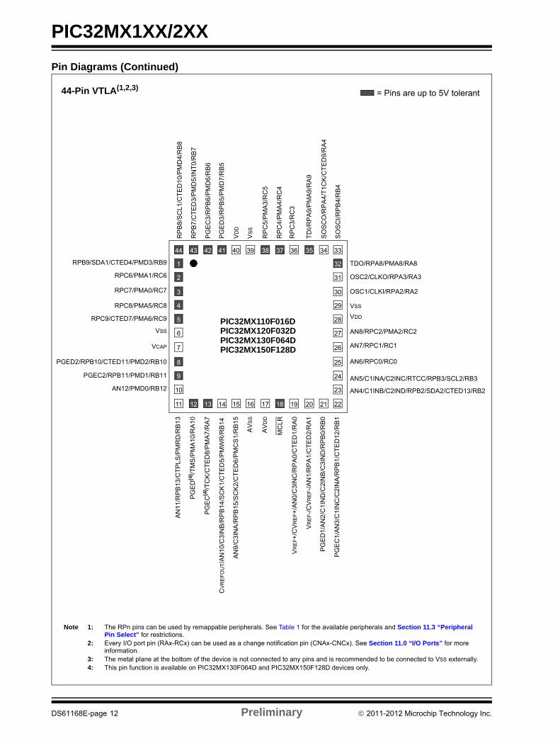
44-Pin VTLA(1,2,3)= Pins are up to 5V tolerant
Note 1: The RPn pins can be used by remappable peripherals. See Table 1 for the available peripherals and Section 11.3 “Peripheral Pin Select” for restrictions.
2: Every I/O port pin (RAx-RCx) can be used as a change notification pin (CNAx-CNCx). See Section 11.0 “I/O Ports” for more information.
3: The metal plane at the bottom of the device is not connected to any pins and is recommended to be connected to VSS externally.4: This pin function is available on PIC32MX130F064D and PIC32MX150F128D devices only.
RP
B8
/SC
L1/
CT
ED
10/
PM
D4
/RB
8
RP
B7
/CT
ED
3/P
MD
5/I
NT
0/R
B7
PG
EC
3/R
PB
6/P
MD
6/R
B6
PG
ED
3/R
PB
5/P
MD
7/R
B5
VD
D
VS
S
RP
C5
/PM
A3
/RC
5
RP
C4
/PM
A4
/RC
4
RP
C3
/RC
3
TD
I/RP
A9
/PM
A9
/RA
9
SO
SC
O/R
PA
4/T
1C
K/C
TE
D9
/RA
4
RPB9/SDA1/CTED4/PMD3/RB9
SO
SC
I/R
PB
4/R
B4
RPC6/PMA1/RC6
TDO/RPA8/PMA8/RA8
RPC7/PMA0/RC7
OSC2/CLKO/RPA3/RA3
RPC8/PMA5/RC8
OSC1/CLKI/RPA2/RA2
RPC9/CTED7/PMA6/RC9
VSS
VSS
PIC32MX110F016DVDD
VCAP
AN8/RPC2/PMA2/RC2
PGED2/RPB10/CTED11/PMD2/RB10
AN7/RPC1/RC1
PGEC2/RPB11/PMD1/RB11
AN6/RPC0/RC0
AN12/PMD0/RB12
AN5/C1INA/C2INC/RTCC/RPB3/SCL2/RB3
AN4/C1INB/C2IND/RPB2/SDA2/CTED13/RB2
PG
EC
(4) /T
CK
/CT
ED
8/P
MA
7/R
A7
CV
RE
FO
UT/A
N1
0/C
3IN
B/R
PB
14
/SC
K1/
CT
ED
5/P
MW
R/R
B1
4
AN
9/C
3IN
A/R
PB
15/
SC
K2
/CT
ED
6/P
MC
S1
/RB
15
AV
SS
AV
DD
MC
LR
VR
EF+
/CV
RE
F+
/AN
0/C
3IN
C/R
PA
0/C
TE
D1
/RA
0
VR
EF-/
CV
RE
F-/
AN
1/R
PA
1/C
TE
D2
/RA
1
PG
ED
1/A
N2
/C1I
ND
/C2
INB
/C3I
ND
/RP
B0/
RB
0PIC32MX120F032D
1
10
33
32
31
30
29
28
2
3
4
5
6
24
23
2221201911 12 13 14 15
7
8
9
343536
16 17 18
27
26
25
3738394041424344
PG
EC
1/A
N3/
C1I
NC
/C2I
NA
/RP
B1
/CT
ED
12
/RB
1
AN
11/
RP
B1
3/C
TP
LS
/PM
RD
/RB
13
PIC32MX130F064DPIC32MX150F128D
PG
ED
(4) /T
MS
/PM
A1
0/R
A1
0
DS61168E-page 12 Preliminary 2011-2012 Microchip Technology Inc.
PIC32MX1XX/2XX
Pin Diagrams (Continued)
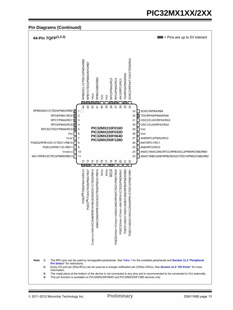
44-Pin TQFP(1,2,3) = Pins are up to 5V tolerant
Note 1: The RPn pins can be used by remappable peripherals. See Table 1 for the available peripherals and Section 11.3 “Peripheral Pin Select” for restrictions.
2: Every I/O port pin (RAx-RCx) can be used as a change notification pin (CNAx-CNCx). See Section 11.0 “I/O Ports” for more information.
3: The metal plane at the bottom of the device is not connected to any pins and is recommended to be connected to VSS externally.4: This pin function is available on PIC32MX230F064D and PIC32MX250F128D devices only.
RP
B8
/SC
L1
/CT
ED
10
/PM
D4
/RB
8
RP
B7
/CT
ED
3/P
MD
5/IN
T0
/RB
7
VB
US
RP
B5
/US
BID
/RB
5
VD
D
VS
S
RP
C5
/PM
A3
/RC
5
RP
C4
/PM
A4
/RC
4
AN
12/R
PC
3/R
C3
TD
I/R
PA
9/P
MA
9/R
A9
SO
SC
O/R
PA
4/T
1C
K/C
TE
D9
/RA
4
44
43
42
41
40
39
38
37
36
35
34
1 33 SOSCI/RPB4/RB4
RPC6/PMA1/RC6 2 32 TDO/RPA8/PMA8/RA8
RPC7/PMA0/RC7 3 31 OSC2/CLKO/RPA3/RA3
RPC8/PMA5/RC8 4 30 OSC1/CLKI/RPA2/RA2
RPC9/CTED7/PMA6/RC9 5 29 VSS
VSS 6
PIC32MX210F016D
28 VDD
VCAP 7 27 AN8/RPC2/PMA2/RC2
8 26 AN7/RPC1/RC1
PGEC2/RPB11/D-/RB11 9 25 AN6/RPC0/RC0
VUSB3V3 10 24 AN5/C1INA/C2INC/RTCC/RPB3/SCL2/PMWR/CNB3/RB3
AN11/RPB13/CTPLS/PMRD/RB13 11 23 AN4/C1INB/C2IND/RPB2/SDA2/CTED13/PMD2/CNB2/RB2
12 13 14 15 16 17 18 19 20 21 22
PG
ED
(4) /T
MS
/PM
A1
0/R
A1
0
PG
EC
(4) /T
CK
/CT
ED
8/P
MA
7/R
A7
CV
RE
FO
UT/A
N1
0/C
3IN
B/R
PB
14
/VB
US
ON
/SC
K1
/CT
ED
5/R
B1
4
AN
9/C
3IN
A/R
PB
15/S
CK
2/C
TE
D6
/PM
CS
1/R
B1
5
AV
SS
AV
DD
MC
LR
PG
ED
3/V
RE
F+
/CV
RE
F+
/AN
0/C
3IN
C/R
PA
0/C
TE
D1
/PM
D7/
RA
0
PG
EC
3/V
RE
F-/
CV
RE
F-/
AN
1/R
PA
1/C
TE
D2
/PM
D6/
RA
1
PG
ED
1/A
N2
/C1
IND
/C2
INB
/C3I
ND
/RP
B0
/PM
D0/
RB
0
PG
EC
1/A
N3
/C1
INC
/C2
INA
/RP
B1
/CT
ED
12
/PM
D1/
RB
1
PGED2/RPB10/D+/CTED11/RB10
RPB9/SDA1/CTED4/PMD3/RB9
PIC32MX220F032DPIC32MX230F064DPIC32MX250F128D
2011-2012 Microchip Technology Inc. Preliminary DS61168E-page 13
PIC32MX1XX/2XX
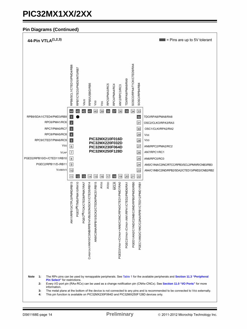
Pin Diagrams (Continued)
44-Pin VTLA(1,2,3) = Pins are up to 5V tolerant
Note 1: The RPn pins can be used by remappable peripherals. See Table 1 for the available peripherals and Section 11.3 “Peripheral Pin Select” for restrictions.
2: Every I/O port pin (RAx-RCx) can be used as a change notification pin (CNAx-CNCx). See Section 11.0 “I/O Ports” for more information.
3: The metal plane at the bottom of the device is not connected to any pins and is recommended to be connected to VSS externally.4: This pin function is available on PIC32MX230F064D and PIC32MX250F128D devices only.
RP
B8/S
CL1
/CT
ED
10/
PM
D4/
RB
8
RP
B7/C
TE
D3/P
MD
5/IN
T0/
RB
7
VB
US
RP
B5/U
SB
ID/R
B5
VD
D
VS
S
RP
C5/
PM
A3/R
C5
RP
C4/
PM
A4/R
C4
AN
12/R
PC
3/R
C3
TD
I/RP
A9/
PM
A9/
RA
9
SO
SC
O/R
PA
4/T
1CK
/CT
ED
9/R
A4
SO
SC
I/RP
B4/
RB
4
RPC6/PMA1/RC6
TDO/RPA8/PMA8/RA8
RPC7/PMA0/RC7
OSC2/CLKO/RPA3/RA3
RPC8/PMA5/RC8
OSC1/CLKI/RPA2/RA2
RPC9/CTED7/PMA6/RC9
VSS
VSS
VDD
VCAP
AN8/RPC2/PMA2/RC2
AN7/RPC1/RC1
PGEC2/RPB11/D-/RB11
AN6/RPC0/RC0
VUSB3V3
AN5/C1INA/C2INC/RTCC/RPB3/SCL2/PMWR/CNB3/RB3
AN
11/R
PB
13/C
TP
LS/P
MR
D/R
B13
AN4/C1INB/C2IND/RPB2/SDA2/CTED13/PMD2/CNB2/RB2
PG
ED
(4) /T
MS
/PM
A10
/RA
10
PG
EC
(4) /T
CK
/CT
ED
8/P
MA
7/R
A7
CV
RE
FO
UT/A
N10/
C3I
NB
/RP
B14
/VB
US
ON
/SC
K1/
CT
ED
5/R
B14
AN
9/C
3IN
A/R
PB
15/S
CK
2/C
TE
D6/
PM
CS
1/R
B15
AV
SS
AV
DD
MC
LR
PG
ED
3/V
RE
F+
/CV
RE
F+
/AN
0/C
3IN
C/R
PA
0/C
TE
D1/
PM
D7/
RA
0
PG
EC
3/V
RE
F-/
CV
RE
F-/
AN
1/R
PA
1/C
TE
D2/
PM
D6/
RA
1
PG
ED
1/A
N2/
C1I
ND
/C2I
NB
/C3I
ND
/RP
B0/
PM
D0/
RB
0
PG
EC
1/A
N3/
C1I
NC
/C2I
NA
/RP
B1/C
TE
D12/
PM
D1/
RB
1
PGED2/RPB10/D+/CTED11/RB10
RPB9/SDA1/CTED4/PMD3/RB9
PIC32MX210F016DPIC32MX220F032D
1
10
33
32
31
30
29
28
2
3
4
5
6
24
23
2221201911 12 13 14 15
7
8
9
343536
16 17 18
27
26
25
3738394041424344
PIC32MX230F064DPIC32MX250F128D
DS61168E-page 14 Preliminary 2011-2012 Microchip Technology Inc.
PIC32MX1XX/2XX
Table of Contents
1.0 Device Overview ........................................................................................................................................................................ 192.0 Guidelines for Getting Started with 32-bit MCUs........................................................................................................................ 273.0 CPU............................................................................................................................................................................................ 314.0 Memory Organization ................................................................................................................................................................. 355.0 Flash Program Memory.............................................................................................................................................................. 776.0 Resets ........................................................................................................................................................................................ 817.0 Interrupt Controller ..................................................................................................................................................................... 858.0 Oscillator Configuration .............................................................................................................................................................. 939.0 Direct Memory Access (DMA) Controller ................................................................................................................................. 10310.0 USB On-The-Go (OTG)............................................................................................................................................................ 11911.0 I/O Ports ................................................................................................................................................................................... 14112.0 Timer1 ...................................................................................................................................................................................... 14913.0 Timer2/3, Timer4/5 ................................................................................................................................................................... 15314.0 Input Capture............................................................................................................................................................................ 15715.0 Output Compare....................................................................................................................................................................... 16116.0 Serial Peripheral Interface (SPI)............................................................................................................................................... 16317.0 Inter-Integrated Circuit™ (I2C™).............................................................................................................................................. 17118.0 Universal Asynchronous Receiver Transmitter (UART) ........................................................................................................... 17719.0 Parallel Master Port (PMP)....................................................................................................................................................... 18320.0 Real-Time Clock and Calendar (RTCC)................................................................................................................................... 19121.0 10-bit Analog-to-Digital Converter (ADC) ................................................................................................................................. 20122.0 Comparator .............................................................................................................................................................................. 20923.0 Comparator Voltage Reference (CVREF) ................................................................................................................................. 21324.0 Charge Time Measurement Unit (CTMU) ............................................................................................................................... 21525.0 Power-Saving Features ........................................................................................................................................................... 21926.0 Special Features ...................................................................................................................................................................... 22327.0 Instruction Set .......................................................................................................................................................................... 23728.0 Development Support............................................................................................................................................................... 23929.0 Electrical Characteristics .......................................................................................................................................................... 24330.0 50 MHz Electrical Characteristics............................................................................................................................................. 28530.0 DC and AC Device Characteristics Graphs.............................................................................................................................. 29131.0 Packaging Information.............................................................................................................................................................. 295The Microchip Web Site..................................................................................................................................................................... 323Customer Change Notification Service .............................................................................................................................................. 323Customer Support .............................................................................................................................................................................. 323Reader Response .............................................................................................................................................................................. 324Product Identification System ............................................................................................................................................................ 325
2011-2012 Microchip Technology Inc. Preliminary DS61168E-page 15
PIC32MX1XX/2XX
TO OUR VALUED CUSTOMERSIt is our intention to provide our valued customers with the best documentation possible to ensure successful use of your Microchipproducts. To this end, we will continue to improve our publications to better suit your needs. Our publications will be refined andenhanced as new volumes and updates are introduced.
If you have any questions or comments regarding this publication, please contact the Marketing Communications Departmentvia E-mail at [email protected] or fax the Reader Response Form in the back of this data sheet to (480) 792-4150.We welcome your feedback.
Most Current Data SheetTo obtain the most up-to-date version of this data sheet, please register at our Worldwide Web site at:
http://www.microchip.com
You can determine the version of a data sheet by examining its literature number found on the bottom outside corner of any page.The last character of the literature number is the version number, (e.g., DS30000A is version A of document DS30000).
ErrataAn errata sheet, describing minor operational differences from the data sheet and recommended workarounds, may exist for currentdevices. As device/documentation issues become known to us, we will publish an errata sheet. The errata will specify the revisionof silicon and revision of document to which it applies.
To determine if an errata sheet exists for a particular device, please check with one of the following:
• Microchip’s Worldwide Web site; http://www.microchip.com• Your local Microchip sales office (see last page)
When contacting a sales office, please specify which device, revision of silicon and data sheet (include literature number) you areusing.
Customer Notification SystemRegister on our web site at www.microchip.com to receive the most current information on all of our products.
DS61168E-page 16 Preliminary 2011-2012 Microchip Technology Inc.
PIC32MX1XX/2XX
Referenced Sources
This device data sheet is based on the followingindividual chapters of the “PIC32 Family ReferenceManual”. These documents should be considered asthe general reference for the operation of a particularmodule or device feature.
• Section 1. “Introduction” (DS61127)
• Section 2. “CPU” (DS61113)
• Section 3. “Memory Organization” (DS61115)
• Section 5. “Flash Program Memory” (DS61121)
• Section 6. “Oscillator Configuration” (DS61112)
• Section 7. “Resets” (DS61118)
• Section 8. “Interrupt Controller” (DS61108)
• Section 9. “Watchdog Timer and Power-up Timer” (DS61114)
• Section 10. “Power-Saving Features” (DS61130)
• Section 12. “I/O Ports” (DS61120)
• Section 13. “Parallel Master Port (PMP)” (DS61128)
• Section 14. “Timers” (DS61105)
• Section 15. “Input Capture” (DS61122)
• Section 16. “Output Compare” (DS61111)
• Section 17. “10-bit Analog-to-Digital Converter (ADC)” (DS61104)
• Section 19. “Comparator” (DS61110)
• Section 20. “Comparator Voltage Reference (CVREF)” (DS61109)
• Section 21. “Universal Asynchronous Receiver Transmitter (UART)” (DS61107)
• Section 23. “Serial Peripheral Interface (SPI)” (DS61106)
• Section 24. “Inter-Integrated Circuit™ (I2C™)” (DS61116)
• Section 27. “USB On-The-Go (OTG)” (DS61126)
• Section 29. “Real-Time Clock and Calendar (RTCC)” (DS61125)
• Section 31. “Direct Memory Access (DMA) Controller” (DS61117)
• Section 32. “Configuration” (DS61124)
• Section 33. “Programming and Diagnostics” (DS61129)
• Section 37. “Charge Time Measurement Unit (CTMU)” (DS61167)
Note: To access the documents listed below,browse to the documentation section ofthe Microchip web site(www.microchip.com).
2011-2012 Microchip Technology Inc. Preliminary DS61168E-page 17

PIC32MX1XX/2XX
NOTES:
DS61168E-page 18 Preliminary 2011-2012 Microchip Technology Inc.
PIC32MX1XX/2XX
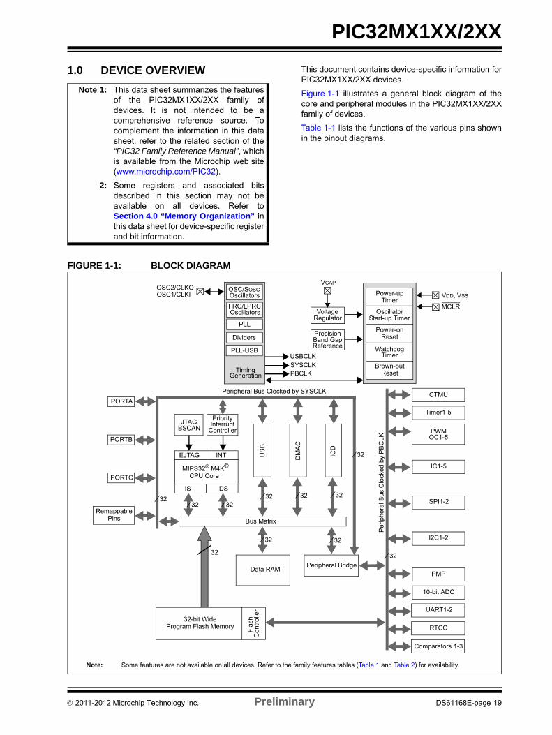
1.0 DEVICE OVERVIEW This document contains device-specific information forPIC32MX1XX/2XX devices.
Figure 1-1 illustrates a general block diagram of thecore and peripheral modules in the PIC32MX1XX/2XXfamily of devices.
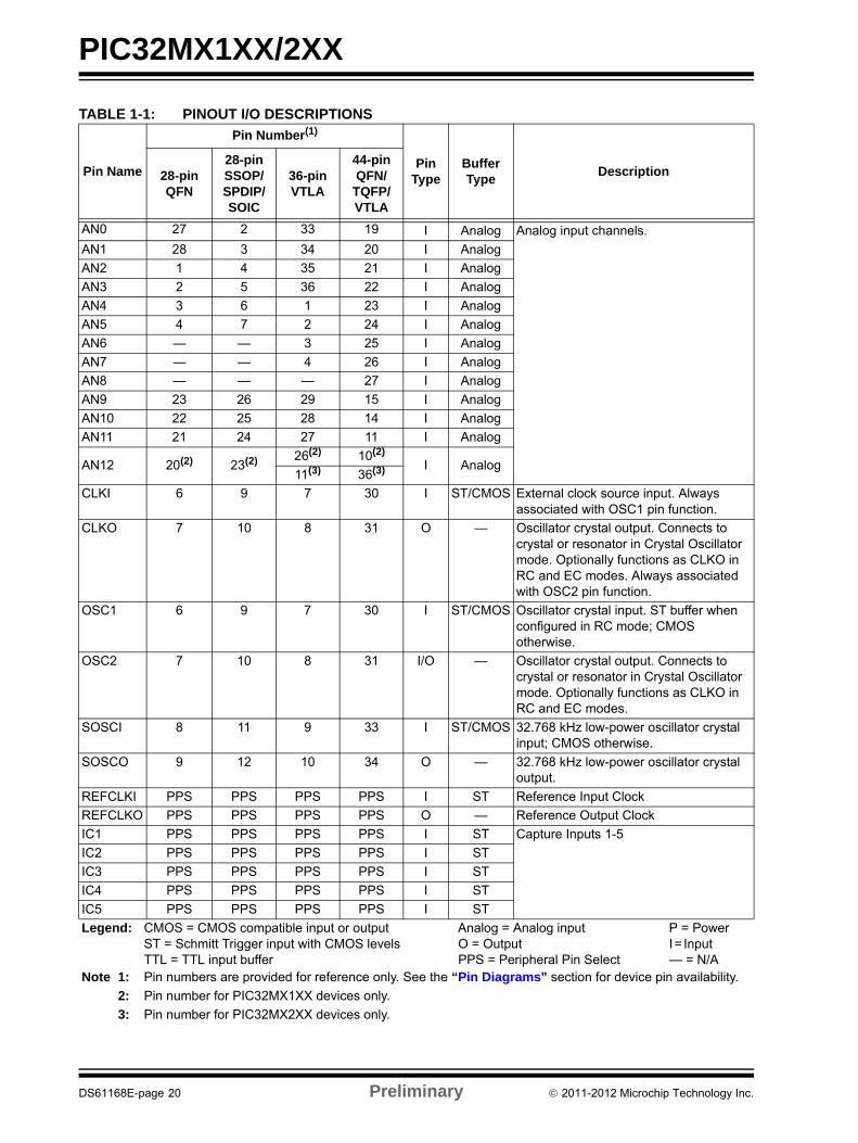
Table 1-1 lists the functions of the various pins shownin the pinout diagrams.
FIGURE 1-1: BLOCK DIAGRAM
Note 1: This data sheet summarizes the featuresof the PIC32MX1XX/2XX family ofdevices. It is not intended to be acomprehensive reference source. Tocomplement the information in this datasheet, refer to the related section of the“PIC32 Family Reference Manual”, whichis available from the Microchip web site(www.microchip.com/PIC32).
2: Some registers and associated bitsdescribed in this section may not beavailable on all devices. Refer toSection 4.0 “Memory Organization” inthis data sheet for device-specific registerand bit information.
Note: Some features are not available on all devices. Refer to the family features tables (Table 1 and Table 2) for availability.
UART1-2
Comparators 1-3
PORTA
Remappable
PORTB
CTMU
JTAGPriority
DM
AC
ICD
MIPS32® M4K®
IS DS
EJTAG INT
Bus Matrix
Data RAMPeripheral Bridge
32
32-bit Wide
Fla
sh
32 32
32 32
Pe
riph
era
l Bu
s C
lock
ed
by
PB
CLK
Program Flash Memory
Co
ntr
olle
r
32
32 32
InterruptControllerBSCAN
PORTC
PMP
I2C1-2
SPI1-2
IC1-5
PWMOC1-5
OSC1/CLKIOSC2/CLKO
VDD, VSS
TimingGeneration
MCLR
Power-upTimer
OscillatorStart-up Timer
Power-onReset
WatchdogTimer
Brown-outReset
Precision
ReferenceBand Gap
FRC/LPRCOscillators
RegulatorVoltage
VCAPOSC/SOSCOscillators
PLL
Dividers
SYSCLKPBCLK
Peripheral Bus Clocked by SYSCLK
US
B
PLL-USBUSBCLK
32
RTCC
10-bit ADC
Timer1-5
32
32
CPU Core
Pins
2011-2012 Microchip Technology Inc. Preliminary DS61168E-page 19
PIC32MX1XX/2XX
TABLE 1-1: PINOUT I/O DESCRIPTIONS
Pin Name
Pin Number(1)
PinType
BufferType
Description28-pin QFN
28-pin SSOP/SPDIP/SOIC
36-pin VTLA
44-pin QFN/
TQFP/VTLA
AN0 27 2 33 19 I Analog Analog input channels.
AN1 28 3 34 20 I Analog
AN2 1 4 35 21 I Analog
AN3 2 5 36 22 I Analog
AN4 3 6 1 23 I Analog
AN5 4 7 2 24 I Analog
AN6 — — 3 25 I Analog
AN7 — — 4 26 I Analog
AN8 — — — 27 I Analog
AN9 23 26 29 15 I Analog
AN10 22 25 28 14 I Analog
AN11 21 24 27 11 I Analog
AN12 20(2) 23(2) 26(2) 10(2)
I Analog11(3) 36(3)
CLKI 6 9 7 30 I ST/CMOS External clock source input. Always associated with OSC1 pin function.
CLKO 7 10 8 31 O — Oscillator crystal output. Connects to crystal or resonator in Crystal Oscillator mode. Optionally functions as CLKO in RC and EC modes. Always associated with OSC2 pin function.
OSC1 6 9 7 30 I ST/CMOS Oscillator crystal input. ST buffer when configured in RC mode; CMOS otherwise.
OSC2 7 10 8 31 I/O — Oscillator crystal output. Connects to crystal or resonator in Crystal Oscillator mode. Optionally functions as CLKO in RC and EC modes.
SOSCI 8 11 9 33 I ST/CMOS 32.768 kHz low-power oscillator crystal input; CMOS otherwise.
SOSCO 9 12 10 34 O — 32.768 kHz low-power oscillator crystal output.
REFCLKI PPS PPS PPS PPS I ST Reference Input Clock
REFCLKO PPS PPS PPS PPS O — Reference Output Clock
IC1 PPS PPS PPS PPS I ST Capture Inputs 1-5
IC2 PPS PPS PPS PPS I ST
IC3 PPS PPS PPS PPS I ST
IC4 PPS PPS PPS PPS I ST
IC5 PPS PPS PPS PPS I ST
Legend: CMOS = CMOS compatible input or output Analog = Analog input P = PowerST = Schmitt Trigger input with CMOS levels O = Output I = Input TTL = TTL input buffer PPS = Peripheral Pin Select — = N/A
Note 1: Pin numbers are provided for reference only. See the “Pin Diagrams” section for device pin availability.
2: Pin number for PIC32MX1XX devices only.
3: Pin number for PIC32MX2XX devices only.
DS61168E-page 20 Preliminary 2011-2012 Microchip Technology Inc.
PIC32MX1XX/2XX
OC1 PPS PPS PPS PPS O — Output Compare Output 1
OC2 PPS PPS PPS PPS O — Output Compare Output 2
OC3 PPS PPS PPS PPS O — Output Compare Output 3
OC4 PPS PPS PPS PPS O — Output Compare Output 4
OC5 PPS PPS PPS PPS O — Output Compare Output 5
OCFA PPS PPS PPS PPS I ST Output Compare Fault A Input
OCFB PPS PPS PPS PPS I ST Output Compare Fault B Input
INT0 13 16 17 43 I ST External Interrupt 0
INT1 PPS PPS PPS PPS I ST External Interrupt 1
INT2 PPS PPS PPS PPS I ST External Interrupt 2
INT3 PPS PPS PPS PPS I ST External Interrupt 3
INT4 PPS PPS PPS PPS I ST External Interrupt 4
RA0 27 2 33 19 I/O ST PORTA is a bidirectional I/O port
RA1 28 3 34 20 I/O ST
RA2 6 9 7 30 I/O ST
RA3 7 10 8 31 I/O ST
RA4 9 12 10 34 I/O ST
RA7 — — — 13 I/O ST
RA8 — — — 32 I/O ST
RA9 — — — 35 I/O ST
RA10 — — — 12 I/O ST
RB0 1 4 35 21 I/O ST PORTB is a bidirectional I/O port
RB1 2 5 36 22 I/O ST
RB2 3 6 1 23 I/O ST
RB3 4 7 2 24 I/O ST
RB4 8 11 9 33 I/O ST
RB5 11 14 15 41 I/O ST
RB6 12(2) 15(2) 16(2) 42(2) I/O ST
RB7 13 16 17 43 I/O ST
RB8 14 17 18 44 I/O ST
RB9 15 18 19 1 I/O ST
RB10 18 21 24 8 I/O ST
RB11 19 22 25 9 I/O ST
RB12 20(2) 23(2) 26(2) 10(2) I/O ST
RB13 21 24 27 11 I/O ST
RB14 22 25 28 14 I/O ST
RB15 23 26 29 15 I/O ST
TABLE 1-1: PINOUT I/O DESCRIPTIONS (CONTINUED)
Pin Name
Pin Number(1)
PinType
BufferType
Description28-pin QFN
28-pin SSOP/SPDIP/SOIC
36-pin VTLA
44-pin QFN/
TQFP/VTLA
Legend: CMOS = CMOS compatible input or output Analog = Analog input P = PowerST = Schmitt Trigger input with CMOS levels O = Output I = Input TTL = TTL input buffer PPS = Peripheral Pin Select — = N/A
Note 1: Pin numbers are provided for reference only. See the “Pin Diagrams” section for device pin availability.
2: Pin number for PIC32MX1XX devices only.
3: Pin number for PIC32MX2XX devices only.
2011-2012 Microchip Technology Inc. Preliminary DS61168E-page 21
PIC32MX1XX/2XX
RC0 — — 3 25 I/O ST PORTC is a bidirectional I/O port
RC1 — — 4 26 I/O ST
RC2 — — — 27 I/O ST
RC3 — — 11 36 I/O ST
RC4 — — — 37 I/O ST
RC5 — — — 38 I/O ST
RC6 — — — 2 I/O ST
RC7 — — — 3 I/O ST
RC8 — — — 4 I/O ST
RC9 — — 20 5 I/O ST
T1CK 9 12 10 34 I ST Timer1 external clock input
T2CK PPS PPS PPS PPS I ST Timer2 external clock input
T3CK PPS PPS PPS PPS I ST Timer3 external clock input
T4CK PPS PPS PPS PPS I ST Timer4 external clock input
T5CK PPS PPS PPS PPS I ST Timer5 external clock input
U1CTS PPS PPS PPS PPS I ST UART1 clear to send
U1RTS PPS PPS PPS PPS O — UART1 ready to send
U1RX PPS PPS PPS PPS I ST UART1 receive
U1TX PPS PPS PPS PPS O — UART1 transmit
U2CTS PPS PPS PPS PPS I ST UART2 clear to send
U2RTS PPS PPS PPS PPS O — UART2 ready to send
U2RX PPS PPS PPS PPS I ST UART2 receive
U2TX PPS PPS PPS PPS O — UART2 transmit
SCK1 22 25 28 14 I/O ST Synchronous serial clock input/output for SPI1
SDI1 PPS PPS PPS PPS I ST SPI1 data in
SDO1 PPS PPS PPS PPS O — SPI1 data out
SS1 PPS PPS PPS PPS I/O ST SPI1 slave synchronization or frame pulse I/O
SCK2 23 26 29 15 I/O ST Synchronous serial clock input/output for SPI2
SDI2 PPS PPS PPS PPS I ST SPI2 data in
SDO2 PPS PPS PPS PPS O — SPI2 data out
SS2 PPS PPS PPS PPS I/O ST SPI2 slave synchronization or frame pulse I/O
SCL1 14 17 18 44 I/O ST Synchronous serial clock input/output for I2C1
TABLE 1-1: PINOUT I/O DESCRIPTIONS (CONTINUED)
Pin Name
Pin Number(1)
PinType
BufferType
Description28-pin QFN
28-pin SSOP/SPDIP/SOIC
36-pin VTLA
44-pin QFN/
TQFP/VTLA
Legend: CMOS = CMOS compatible input or output Analog = Analog input P = PowerST = Schmitt Trigger input with CMOS levels O = Output I = Input TTL = TTL input buffer PPS = Peripheral Pin Select — = N/A
Note 1: Pin numbers are provided for reference only. See the “Pin Diagrams” section for device pin availability.
2: Pin number for PIC32MX1XX devices only.
3: Pin number for PIC32MX2XX devices only.
DS61168E-page 22 Preliminary 2011-2012 Microchip Technology Inc.
PIC32MX1XX/2XX
SDA1 15 18 19 1 I/O ST Synchronous serial data input/output for I2C1
SCL2 4 7 2 24 I/O ST Synchronous serial clock input/output for I2C2
SDA2 3 6 1 23 I/O ST Synchronous serial data input/output for I2C2
TMS19(2) 22(2) 25(2)
12 I ST JTAG Test mode select pin11(3) 14(3) 15(3)
TCK 14 17 18 13 I ST JTAG test clock input pin
TDI 13 16 17 35 O — JTAG test data input pin
TDO 15 18 19 32 O — JTAG test data output pin
RTCC 4 7 2 24 I ST Real-Time Clock alarm output
CVREF- 28 3 34 20 I Analog Comparator Voltage Reference (low)
CVREF+ 27 2 33 19 I Analog Comparator Voltage Reference (high)
CVREFOUT 22 25 28 14 O Analog Comparator Voltage Reference output
C1INA 4 7 2 24 I Analog Comparator Inputs
C1INB 3 6 1 23 I Analog
C1INC 2 5 36 22 I Analog
C1IND 1 4 35 21 I Analog
C2INA 2 5 36 22 I Analog
C2INB 1 4 35 21 I Analog
C2INC 4 7 2 24 I Analog
C2IND 3 6 1 23 I Analog
C3INA 23 26 29 15 I Analog
C3INB 22 25 28 14 I Analog
C3INC 27 2 33 19 I Analog
C3IND 1 4 35 21 I Analog
C1OUT PPS PPS PPS PPS O — Comparator Outputs
C2OUT PPS PPS PPS PPS O —
C3OUT PPS PPS PPS PPS O —
TABLE 1-1: PINOUT I/O DESCRIPTIONS (CONTINUED)
Pin Name
Pin Number(1)
PinType
BufferType
Description28-pin QFN
28-pin SSOP/SPDIP/SOIC
36-pin VTLA
44-pin QFN/
TQFP/VTLA
Legend: CMOS = CMOS compatible input or output Analog = Analog input P = PowerST = Schmitt Trigger input with CMOS levels O = Output I = Input TTL = TTL input buffer PPS = Peripheral Pin Select — = N/A
Note 1: Pin numbers are provided for reference only. See the “Pin Diagrams” section for device pin availability.
2: Pin number for PIC32MX1XX devices only.
3: Pin number for PIC32MX2XX devices only.
2011-2012 Microchip Technology Inc. Preliminary DS61168E-page 23
PIC32MX1XX/2XX
PMA0 7 10 8 3 I/O TTL/ST Parallel Master Port Address bit 0 input (Buffered Slave modes) and output (Master modes)
PMA1 9 12 10 2 I/O TTL/ST Parallel Master Port Address bit 1 input (Buffered Slave modes) and output (Master modes)
PMA2 — — 27 O — Parallel Master Port address (Demultiplexed Master modes)PMA3 — — 38 O —
PMA4 — — 37 O —
PMA5 — — 4 O —
PMA6 — — 5 O —
PMA7 — — 13 O —
PMA8 — — 32 O —
PMA9 — — 35 O —
PMA10 — — 12 O —
PMCS1 23 26 29 15 O — Parallel Master Port Chip Select 1 strobe
PMD020(2) 23(2) 26(2) 10(2)
I/O TTL/STParallel Master Port data (Demultiplexed Master mode) or address/data (Multiplexed Master modes)
1(3) 4(3) 35(3) 21(3)
PMD119(2) 22(2) 25(2) 9(2)
I/O TTL/ST2(3) 5(3) 36(3) 22(3)
PMD218(2) 21(2) 24(2) 8(2)
I/O TTL/ST3(3) 6(3) 1(3) 23(3)
PMD3 15 18 19 1 I/O TTL/ST
PMD4 14 17 18 44 I/O TTL/ST
PMD5 13 16 17 43 I/O TTL/ST
PMD6 12(2) 15(2) 16(2) 42(2)
I/O TTL/ST28(3) 3(3) 34(3) 20(3)
PMD7 11(2) 14(2) 15(2) 41(2)
I/O TTL/ST27(3) 2(3) 33(3) 19(3)
PMRD 21 24 27 11 O — Parallel Master Port read strobe
PMWR22(2) 25(2) 28(2) 14(2)
O — Parallel Master Port write strobe4(3) 7(3) 2(3) 24(3)
VBUS 12 15 16 42 I Analog USB bus power monitor
VUSB3V3 20 23 26 10 P — USB internal transceiver supply. If the USB module is not used, this pin must be connected to VDD.
VBUSON 22 25 28 14 O — USB Host and OTG bus power control output
D+ 18 21 24 8 I/O Analog USB D+
D- 19 22 25 9 I/O Analog USB D-
TABLE 1-1: PINOUT I/O DESCRIPTIONS (CONTINUED)
Pin Name
Pin Number(1)
PinType
BufferType
Description28-pin QFN
28-pin SSOP/SPDIP/SOIC
36-pin VTLA
44-pin QFN/
TQFP/VTLA
Legend: CMOS = CMOS compatible input or output Analog = Analog input P = PowerST = Schmitt Trigger input with CMOS levels O = Output I = Input TTL = TTL input buffer PPS = Peripheral Pin Select — = N/A
Note 1: Pin numbers are provided for reference only. See the “Pin Diagrams” section for device pin availability.
2: Pin number for PIC32MX1XX devices only.
3: Pin number for PIC32MX2XX devices only.
DS61168E-page 24 Preliminary 2011-2012 Microchip Technology Inc.
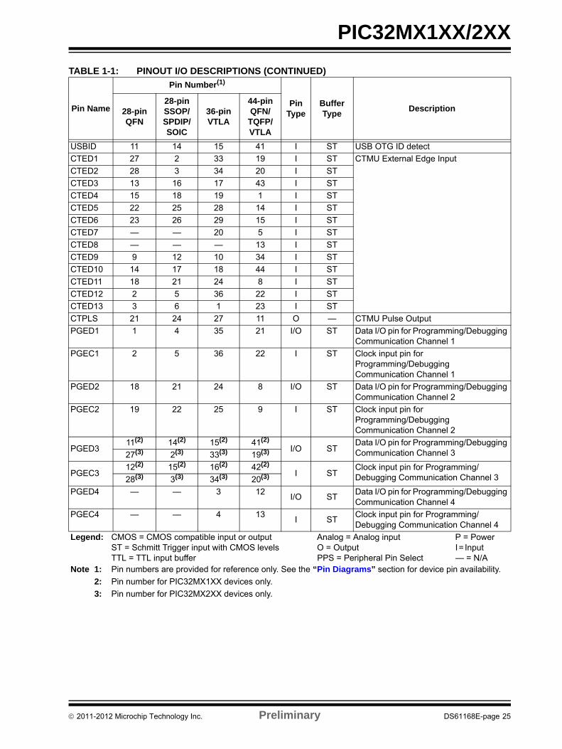
PIC32MX1XX/2XX
USBID 11 14 15 41 I ST USB OTG ID detect
CTED1 27 2 33 19 I ST CTMU External Edge Input
CTED2 28 3 34 20 I ST
CTED3 13 16 17 43 I ST
CTED4 15 18 19 1 I ST
CTED5 22 25 28 14 I ST
CTED6 23 26 29 15 I ST
CTED7 — — 20 5 I ST
CTED8 — — — 13 I ST
CTED9 9 12 10 34 I ST
CTED10 14 17 18 44 I ST
CTED11 18 21 24 8 I ST
CTED12 2 5 36 22 I ST
CTED13 3 6 1 23 I ST
CTPLS 21 24 27 11 O — CTMU Pulse Output
PGED1 1 4 35 21 I/O ST Data I/O pin for Programming/Debugging Communication Channel 1
PGEC1 2 5 36 22 I ST Clock input pin for Programming/Debugging Communication Channel 1
PGED2 18 21 24 8 I/O ST Data I/O pin for Programming/Debugging Communication Channel 2
PGEC2 19 22 25 9 I ST Clock input pin for Programming/Debugging Communication Channel 2
PGED311(2) 14(2) 15(2) 41(2)
I/O STData I/O pin for Programming/Debugging Communication Channel 327(3) 2(3) 33(3) 19(3)
PGEC312(2) 15(2) 16(2) 42(2)
I STClock input pin for Programming/Debugging Communication Channel 328(3) 3(3) 34(3) 20(3)
PGED4 — — 3 12I/O ST
Data I/O pin for Programming/Debugging Communication Channel 4
PGEC4 — — 4 13I ST
Clock input pin for Programming/Debugging Communication Channel 4
TABLE 1-1: PINOUT I/O DESCRIPTIONS (CONTINUED)
Pin Name
Pin Number(1)
PinType
BufferType
Description28-pin QFN
28-pin SSOP/SPDIP/SOIC
36-pin VTLA
44-pin QFN/
TQFP/VTLA
Legend: CMOS = CMOS compatible input or output Analog = Analog input P = PowerST = Schmitt Trigger input with CMOS levels O = Output I = Input TTL = TTL input buffer PPS = Peripheral Pin Select — = N/A
Note 1: Pin numbers are provided for reference only. See the “Pin Diagrams” section for device pin availability.
2: Pin number for PIC32MX1XX devices only.
3: Pin number for PIC32MX2XX devices only.
2011-2012 Microchip Technology Inc. Preliminary DS61168E-page 25
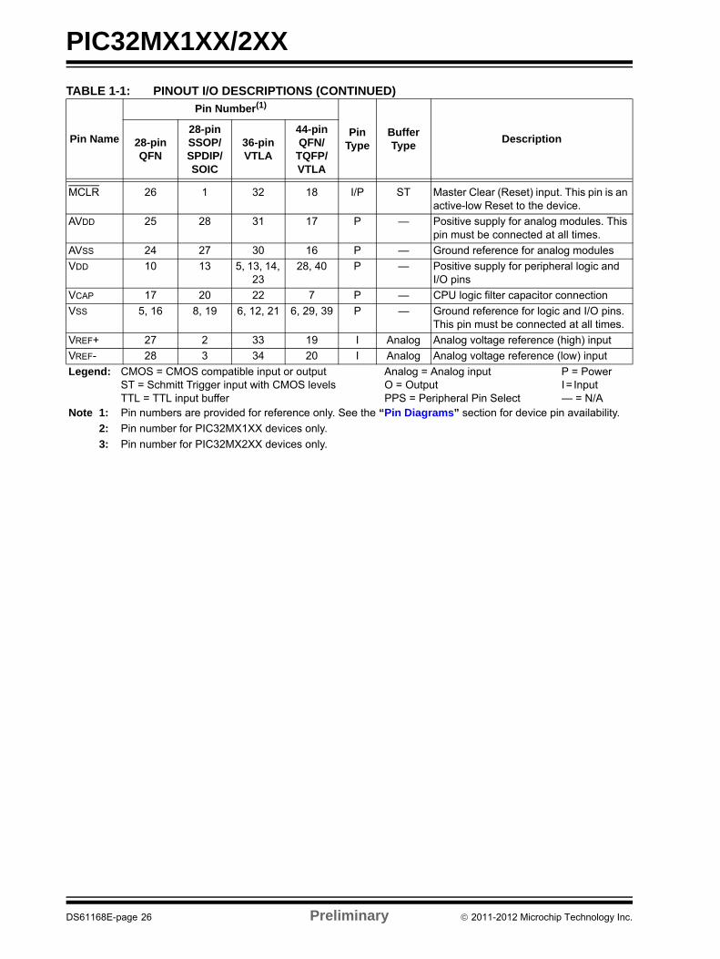
PIC32MX1XX/2XX
MCLR 26 1 32 18 I/P ST Master Clear (Reset) input. This pin is an active-low Reset to the device.
AVDD 25 28 31 17 P — Positive supply for analog modules. This pin must be connected at all times.
AVSS 24 27 30 16 P — Ground reference for analog modules
VDD 10 13 5, 13, 14, 23
28, 40 P — Positive supply for peripheral logic and I/O pins
VCAP 17 20 22 7 P — CPU logic filter capacitor connection
VSS 5, 16 8, 19 6, 12, 21 6, 29, 39 P — Ground reference for logic and I/O pins. This pin must be connected at all times.
VREF+ 27 2 33 19 I Analog Analog voltage reference (high) input
VREF- 28 3 34 20 I Analog Analog voltage reference (low) input
TABLE 1-1: PINOUT I/O DESCRIPTIONS (CONTINUED)
Pin Name
Pin Number(1)
PinType
BufferType
Description28-pin QFN
28-pin SSOP/SPDIP/SOIC
36-pin VTLA
44-pin QFN/
TQFP/VTLA
Legend: CMOS = CMOS compatible input or output Analog = Analog input P = PowerST = Schmitt Trigger input with CMOS levels O = Output I = Input TTL = TTL input buffer PPS = Peripheral Pin Select — = N/A
Note 1: Pin numbers are provided for reference only. See the “Pin Diagrams” section for device pin availability.
2: Pin number for PIC32MX1XX devices only.
3: Pin number for PIC32MX2XX devices only.
DS61168E-page 26 Preliminary 2011-2012 Microchip Technology Inc.
PIC32MX1XX/2XX
2.0 GUIDELINES FOR GETTING STARTED WITH 32-BIT MCUS
2.1 Basic Connection Requirements
Getting started with the PIC32MX1XX/2XX family of32-bit Microcontrollers (MCUs) requires attention to aminimal set of device pin connections before proceed-ing with development. The following is a list of pinnames, which must always be connected:
• All VDD and VSS pins (see 2.2 “Decoupling Capacitors”)
• All AVDD and AVSS pins, even if the ADC module is not used (see 2.2 “Decoupling Capacitors”)
• VCAP pin (see 2.3 “Capacitor on Internal Voltage Regulator (VCAP)”)
• MCLR pin (see 2.4 “Master Clear (MCLR) Pin”)
• PGECx/PGEDx pins, used for In-Circuit Serial Programming (ICSP™) and debugging purposes
• (see 2.5 “ICSP Pins”)
• OSC1 and OSC2 pins, when external oscillator source is used (see 2.7 “External Oscillator Pins”)
The following pin may be required, as well:
• VREF+/VREF- pins – used when external voltage reference for the ADC module is implemented.
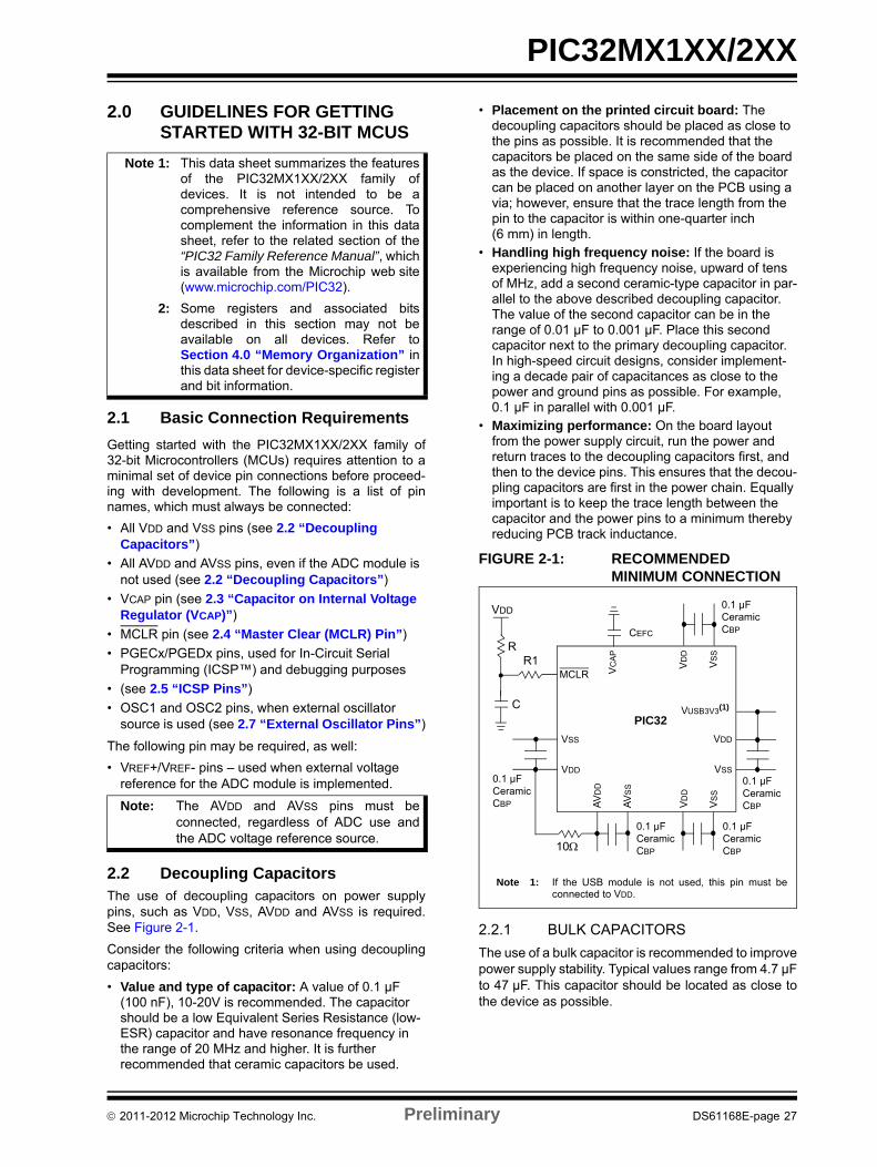
2.2 Decoupling CapacitorsThe use of decoupling capacitors on power supplypins, such as VDD, VSS, AVDD and AVSS is required.See Figure 2-1.
Consider the following criteria when using decouplingcapacitors:
• Value and type of capacitor: A value of 0.1 µF (100 nF), 10-20V is recommended. The capacitor should be a low Equivalent Series Resistance (low-ESR) capacitor and have resonance frequency in the range of 20 MHz and higher. It is further recommended that ceramic capacitors be used.
• Placement on the printed circuit board: The decoupling capacitors should be placed as close to the pins as possible. It is recommended that the capacitors be placed on the same side of the board as the device. If space is constricted, the capacitor can be placed on another layer on the PCB using a via; however, ensure that the trace length from the pin to the capacitor is within one-quarter inch (6 mm) in length.
• Handling high frequency noise: If the board is experiencing high frequency noise, upward of tens of MHz, add a second ceramic-type capacitor in par-allel to the above described decoupling capacitor. The value of the second capacitor can be in the range of 0.01 µF to 0.001 µF. Place this second capacitor next to the primary decoupling capacitor. In high-speed circuit designs, consider implement-ing a decade pair of capacitances as close to the power and ground pins as possible. For example, 0.1 µF in parallel with 0.001 µF.
• Maximizing performance: On the board layout from the power supply circuit, run the power and return traces to the decoupling capacitors first, and then to the device pins. This ensures that the decou-pling capacitors are first in the power chain. Equally important is to keep the trace length between the capacitor and the power pins to a minimum thereby reducing PCB track inductance.
FIGURE 2-1: RECOMMENDED MINIMUM CONNECTION
2.2.1 BULK CAPACITORS
The use of a bulk capacitor is recommended to improvepower supply stability. Typical values range from 4.7 µFto 47 µF. This capacitor should be located as close tothe device as possible.
Note 1: This data sheet summarizes the featuresof the PIC32MX1XX/2XX family ofdevices. It is not intended to be acomprehensive reference source. Tocomplement the information in this datasheet, refer to the related section of the“PIC32 Family Reference Manual”, whichis available from the Microchip web site(www.microchip.com/PIC32).
2: Some registers and associated bitsdescribed in this section may not beavailable on all devices. Refer toSection 4.0 “Memory Organization” inthis data sheet for device-specific registerand bit information.
Note: The AVDD and AVSS pins must beconnected, regardless of ADC use andthe ADC voltage reference source.
PIC32
VD
D
VS
S
VDD
VSS
VSS
VDD
AV
DD
AV
SS
VD
D
VS
SC
R
VDD
MCLR
0.1 µFCeramic
VC
AP
10
R1
CBP
0.1 µFCeramicCBP
0.1 µFCeramicCBP
0.1 µFCeramicCBP
0.1 µFCeramicCBP
CEFC
VUSB3V3(1)
Note 1: If the USB module is not used, this pin must beconnected to VDD.
2011-2012 Microchip Technology Inc. Preliminary DS61168E-page 27
PIC32MX1XX/2XX
2.3 Capacitor on Internal Voltage Regulator (VCAP)
2.3.1 INTERNAL REGULATOR MODE
A low-ESR (1 ohm) capacitor is required on the VCAP
pin, which is used to stabilize the internal voltage regu-lator output. The VCAP pin must not be connected toVDD, and must have a CEFC capacitor, with at least a6V rating, connected to ground. The type can beceramic or tantalum. Refer to Section 29.0 “ElectricalCharacteristics” for additional information on CEFC
specifications.
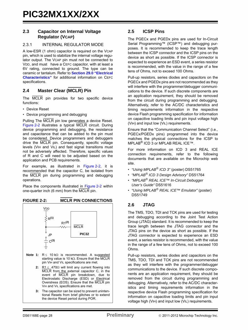
2.4 Master Clear (MCLR) Pin
The MCLR pin provides for two specific devicefunctions:
• Device Reset
• Device programming and debugging
Pulling The MCLR pin low generates a device Reset.Figure 2-2 illustrates a typical MCLR circuit. Duringdevice programming and debugging, the resistanceand capacitance that can be added to the pin mustbe considered. Device programmers and debuggersdrive the MCLR pin. Consequently, specific voltagelevels (VIH and VIL) and fast signal transitions mustnot be adversely affected. Therefore, specific valuesof R and C will need to be adjusted based on theapplication and PCB requirements.
For example, as illustrated in Figure 2-2, it isrecommended that the capacitor C, be isolated fromthe MCLR pin during programming and debuggingoperations.
Place the components illustrated in Figure 2-2 withinone-quarter inch (6 mm) from the MCLR pin.
FIGURE 2-2: MCLR PIN CONNECTIONS
2.5 ICSP Pins
The PGECx and PGEDx pins are used for In-CircuitSerial Programming™ (ICSP™) and debugging pur-poses. It is recommended to keep the trace lengthbetween the ICSP connector and the ICSP pins on thedevice as short as possible. If the ICSP connector isexpected to experience an ESD event, a series resistoris recommended, with the value in the range of a fewtens of Ohms, not to exceed 100 Ohms.
Pull-up resistors, series diodes and capacitors on thePGECx and PGEDx pins are not recommended as theywill interfere with the programmer/debugger communi-cations to the device. If such discrete components arean application requirement, they should be removedfrom the circuit during programming and debugging.Alternatively, refer to the AC/DC characteristics andtiming requirements information in the respectivedevice Flash programming specification for informationon capacitive loading limits and pin input voltage high(VIH) and input low (VIL) requirements.
Ensure that the “Communication Channel Select” (i.e.,PGECx/PGEDx pins) programmed into the devicematches the physical connections for the ICSP toMPLAB® ICD 3 or MPLAB REAL ICE™.
For more information on ICD 3 and REAL ICEconnection requirements, refer to the followingdocuments that are available on the Microchip website.
• “Using MPLAB® ICD 3” (poster) DS51765
• “MPLAB® ICD 3 Design Advisory” DS51764
• “MPLAB® REAL ICE™ In-Circuit Debugger User’s Guide” DS51616
• “Using MPLAB® REAL ICE™ Emulator” (poster) DS51749
2.6 JTAG
The TMS, TDO, TDI and TCK pins are used for testingand debugging according to the Joint Test ActionGroup (JTAG) standard. It is recommended to keep thetrace length between the JTAG connector and theJTAG pins on the device as short as possible. If theJTAG connector is expected to experience an ESDevent, a series resistor is recommended, with the valuein the range of a few tens of Ohms, not to exceed 100Ohms.
Pull-up resistors, series diodes and capacitors on theTMS, TDO, TDI and TCK pins are not recommendedas they will interfere with the programmer/debuggercommunications to the device. If such discrete compo-nents are an application requirement, they should beremoved from the circuit during programming anddebugging. Alternatively, refer to the AC/DC character-istics and timing requirements information in therespective device Flash programming specification forinformation on capacitive loading limits and pin inputvoltage high (VIH) and input low (VIL) requirements.
Note 1: R 10 k is recommended. A suggestedstarting value is 10 k. Ensure that the MCLRpin VIH and VIL specifications are met.
2: R1 470 will limit any current flowing intoMCLR from the external capacitor C, in theevent of MCLR pin breakdown, due toElectrostatic Discharge (ESD) or ElectricalOverstress (EOS). Ensure that the MCLR pinVIH and VIL specifications are met.
3: The capacitor can be sized to prevent uninten-tional Resets from brief glitches or to extendthe device Reset period during POR.
C(3)
R1(2)R(1)
VDD
MCLR
PIC32JP
DS61168E-page 28 Preliminary 2011-2012 Microchip Technology Inc.
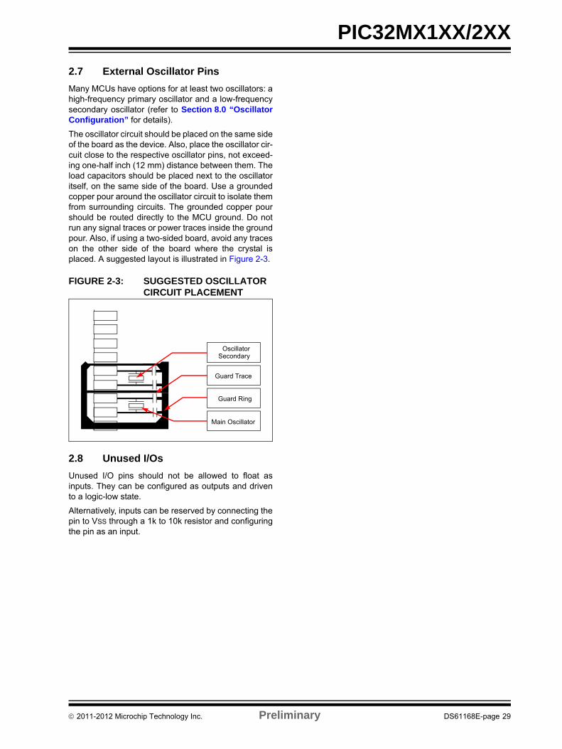
PIC32MX1XX/2XX
2.7 External Oscillator Pins
Many MCUs have options for at least two oscillators: ahigh-frequency primary oscillator and a low-frequencysecondary oscillator (refer to Section 8.0 “OscillatorConfiguration” for details).
The oscillator circuit should be placed on the same sideof the board as the device. Also, place the oscillator cir-cuit close to the respective oscillator pins, not exceed-ing one-half inch (12 mm) distance between them. Theload capacitors should be placed next to the oscillatoritself, on the same side of the board. Use a groundedcopper pour around the oscillator circuit to isolate themfrom surrounding circuits. The grounded copper pourshould be routed directly to the MCU ground. Do notrun any signal traces or power traces inside the groundpour. Also, if using a two-sided board, avoid any traceson the other side of the board where the crystal isplaced. A suggested layout is illustrated in Figure 2-3.
FIGURE 2-3: SUGGESTED OSCILLATOR CIRCUIT PLACEMENT
2.8 Unused I/Os
Unused I/O pins should not be allowed to float asinputs. They can be configured as outputs and drivento a logic-low state.
Alternatively, inputs can be reserved by connecting thepin to VSS through a 1k to 10k resistor and configuringthe pin as an input.
Main Oscillator
Guard Ring
Guard Trace
SecondaryOscillator
2011-2012 Microchip Technology Inc. Preliminary DS61168E-page 29
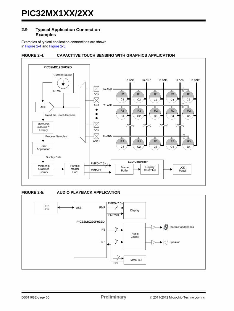
PIC32MX1XX/2XX
2.9 Typical Application Connection Examples
Examples of typical application connections are shownin Figure 2-4 and Figure 2-5.
FIGURE 2-4: CAPACITIVE TOUCH SENSING WITH GRAPHICS APPLICATION
FIGURE 2-5: AUDIO PLAYBACK APPLICATION
CTMU
Current Source
ADC
MicrochipmTouch™
Library
UserApplication
MicrochipGraphicsLibrary
Read the Touch Sensors
Process Samples
Display Data
ParallelMaster
Port
LCD Controller
FrameBuffer
DisplayController
PMPD<7:0>
LCDPanel
PIC32MX120F032D
To AN6 To AN7 To AN8 To AN11
C1
R3
C2
R2
R3
R1
C5
C5
C5C1
R1 R1 R1
C3
R2
C3
R2
C1
R2
C2
R3
C2
R3
C3
AN0
AN1
AN11
To AN0
To AN1
To AN5
AN9
PMPWR
To AN9
R1
C4
R2
C4
R3
C4
AudioCodec
DisplayPMP
I2S
SPI
USBUSB
PMPD<7:0>
3
3
Stereo Headphones
Speaker
PIC32MX220F032D
Host
PMPWR
MMC SD3
SDI
DS61168E-page 30 Preliminary 2011-2012 Microchip Technology Inc.
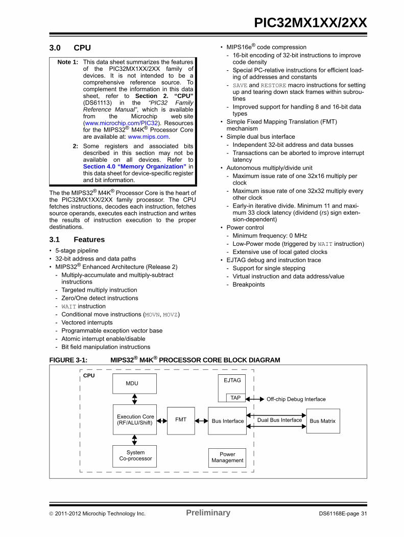
PIC32MX1XX/2XX
3.0 CPU
The the MIPS32® M4K® Processor Core is the heart ofthe PIC32MX1XX/2XX family processor. The CPUfetches instructions, decodes each instruction, fetchessource operands, executes each instruction and writesthe results of instruction execution to the properdestinations.
3.1 Features
• 5-stage pipeline• 32-bit address and data paths• MIPS32® Enhanced Architecture (Release 2)
- Multiply-accumulate and multiply-subtract instructions
- Targeted multiply instruction- Zero/One detect instructions- WAIT instruction- Conditional move instructions (MOVN, MOVZ)- Vectored interrupts- Programmable exception vector base- Atomic interrupt enable/disable- Bit field manipulation instructions
• MIPS16e® code compression- 16-bit encoding of 32-bit instructions to improve
code density- Special PC-relative instructions for efficient load-
ing of addresses and constants- SAVE and RESTORE macro instructions for setting
up and tearing down stack frames within subrou-tines
- Improved support for handling 8 and 16-bit data types
• Simple Fixed Mapping Translation (FMT)mechanism
• Simple dual bus interface- Independent 32-bit address and data busses- Transactions can be aborted to improve interrupt
latency• Autonomous multiply/divide unit
- Maximum issue rate of one 32x16 multiply per clock
- Maximum issue rate of one 32x32 multiply every other clock
- Early-in iterative divide. Minimum 11 and maxi-mum 33 clock latency (dividend (rs) sign exten-sion-dependent)
• Power control- Minimum frequency: 0 MHz- Low-Power mode (triggered by WAIT instruction)- Extensive use of local gated clocks
• EJTAG debug and instruction trace- Support for single stepping- Virtual instruction and data address/value- Breakpoints
FIGURE 3-1: MIPS32® M4K® PROCESSOR CORE BLOCK DIAGRAM
Note 1: This data sheet summarizes the featuresof the PIC32MX1XX/2XX family ofdevices. It is not intended to be acomprehensive reference source. Tocomplement the information in this datasheet, refer to Section 2. “CPU”(DS61113) in the “PIC32 FamilyReference Manual”, which is availablefrom the Microchip web site(www.microchip.com/PIC32). Resourcesfor the MIPS32® M4K® Processor Coreare available at: www.mips.com.
2: Some registers and associated bitsdescribed in this section may not beavailable on all devices. Refer toSection 4.0 “Memory Organization” inthis data sheet for device-specific registerand bit information.
CPU
MDU
Execution Core(RF/ALU/Shift)
FMT
TAP
EJTAG
Bus Interface
PowerManagement
SystemCo-processor
Off-chip Debug Interface
Bus MatrixDual Bus Interface
2011-2012 Microchip Technology Inc. Preliminary DS61168E-page 31
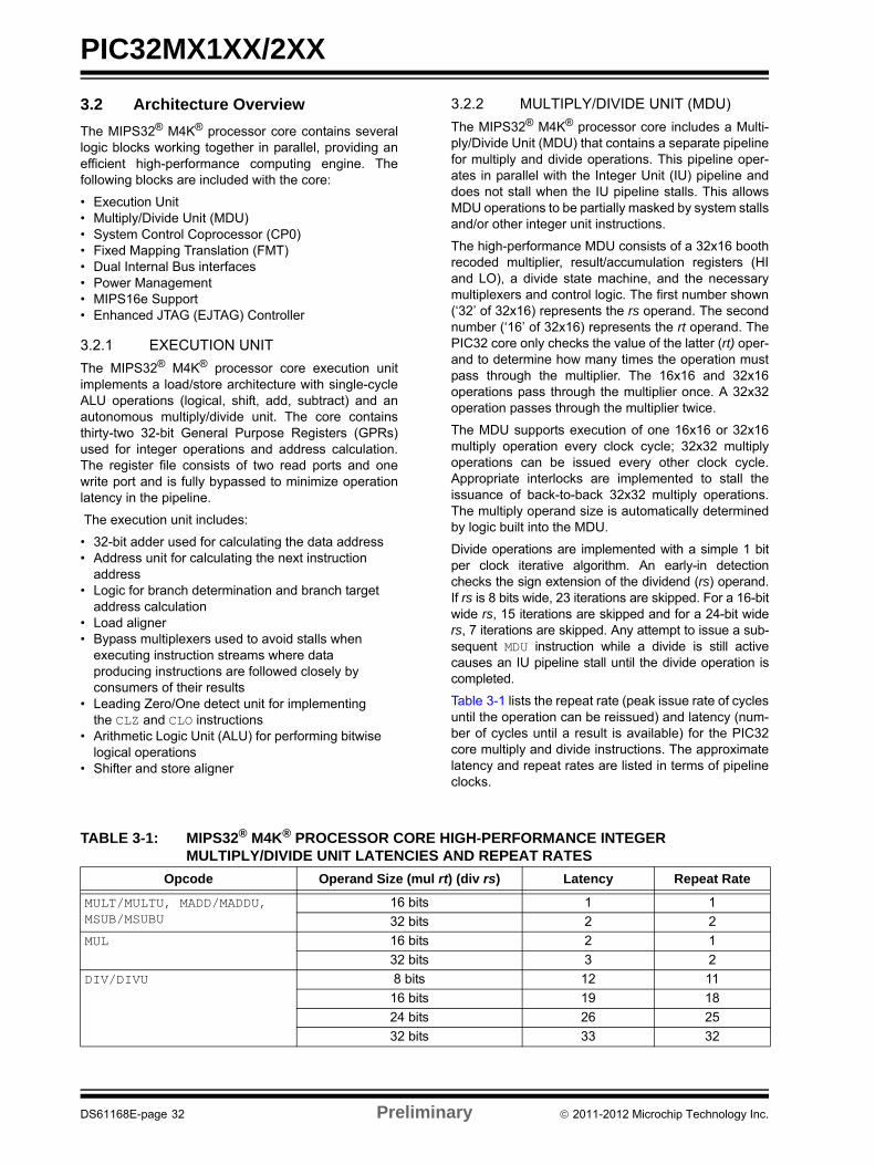
PIC32MX1XX/2XX
3.2 Architecture Overview
The MIPS32® M4K® processor core contains severallogic blocks working together in parallel, providing anefficient high-performance computing engine. Thefollowing blocks are included with the core:
• Execution Unit• Multiply/Divide Unit (MDU)• System Control Coprocessor (CP0)• Fixed Mapping Translation (FMT)• Dual Internal Bus interfaces• Power Management• MIPS16e Support• Enhanced JTAG (EJTAG) Controller
3.2.1 EXECUTION UNIT
The MIPS32® M4K® processor core execution unitimplements a load/store architecture with single-cycleALU operations (logical, shift, add, subtract) and anautonomous multiply/divide unit. The core containsthirty-two 32-bit General Purpose Registers (GPRs)used for integer operations and address calculation.The register file consists of two read ports and onewrite port and is fully bypassed to minimize operationlatency in the pipeline.
The execution unit includes:
• 32-bit adder used for calculating the data address• Address unit for calculating the next instruction
address• Logic for branch determination and branch target
address calculation• Load aligner• Bypass multiplexers used to avoid stalls when
executing instruction streams where data producing instructions are followed closely by consumers of their results
• Leading Zero/One detect unit for implementing the CLZ and CLO instructions
• Arithmetic Logic Unit (ALU) for performing bitwise logical operations
• Shifter and store aligner
3.2.2 MULTIPLY/DIVIDE UNIT (MDU)
The MIPS32® M4K® processor core includes a Multi-ply/Divide Unit (MDU) that contains a separate pipelinefor multiply and divide operations. This pipeline oper-ates in parallel with the Integer Unit (IU) pipeline anddoes not stall when the IU pipeline stalls. This allowsMDU operations to be partially masked by system stallsand/or other integer unit instructions.
The high-performance MDU consists of a 32x16 boothrecoded multiplier, result/accumulation registers (HIand LO), a divide state machine, and the necessarymultiplexers and control logic. The first number shown(‘32’ of 32x16) represents the rs operand. The secondnumber (‘16’ of 32x16) represents the rt operand. ThePIC32 core only checks the value of the latter (rt) oper-and to determine how many times the operation mustpass through the multiplier. The 16x16 and 32x16operations pass through the multiplier once. A 32x32operation passes through the multiplier twice.
The MDU supports execution of one 16x16 or 32x16multiply operation every clock cycle; 32x32 multiplyoperations can be issued every other clock cycle.Appropriate interlocks are implemented to stall theissuance of back-to-back 32x32 multiply operations.The multiply operand size is automatically determinedby logic built into the MDU.
Divide operations are implemented with a simple 1 bitper clock iterative algorithm. An early-in detectionchecks the sign extension of the dividend (rs) operand.If rs is 8 bits wide, 23 iterations are skipped. For a 16-bitwide rs, 15 iterations are skipped and for a 24-bit widers, 7 iterations are skipped. Any attempt to issue a sub-sequent MDU instruction while a divide is still activecauses an IU pipeline stall until the divide operation iscompleted.
Table 3-1 lists the repeat rate (peak issue rate of cyclesuntil the operation can be reissued) and latency (num-ber of cycles until a result is available) for the PIC32core multiply and divide instructions. The approximatelatency and repeat rates are listed in terms of pipelineclocks.
TABLE 3-1: MIPS32® M4K® PROCESSOR CORE HIGH-PERFORMANCE INTEGER MULTIPLY/DIVIDE UNIT LATENCIES AND REPEAT RATES
Opcode Operand Size (mul rt) (div rs) Latency Repeat Rate
MULT/MULTU, MADD/MADDU, MSUB/MSUBU
16 bits 1 1
32 bits 2 2
MUL 16 bits 2 1
32 bits 3 2
DIV/DIVU 8 bits 12 11
16 bits 19 18
24 bits 26 25
32 bits 33 32
DS61168E-page 32 Preliminary 2011-2012 Microchip Technology Inc.
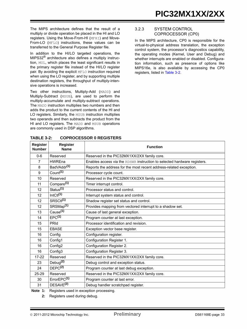
PIC32MX1XX/2XX
The MIPS architecture defines that the result of amultiply or divide operation be placed in the HI and LOregisters. Using the Move-From-HI (MFHI) and Move-From-LO (MFLO) instructions, these values can betransferred to the General Purpose Register file.
In addition to the HI/LO targeted operations, theMIPS32® architecture also defines a multiply instruc-tion, MUL, which places the least significant results inthe primary register file instead of the HI/LO registerpair. By avoiding the explicit MFLO instruction requiredwhen using the LO register, and by supporting multipledestination registers, the throughput of multiply-inten-sive operations is increased.
Two other instructions, Multiply-Add (MADD) andMultiply-Subtract (MSUB), are used to perform themultiply-accumulate and multiply-subtract operations.The MADD instruction multiplies two numbers and thenadds the product to the current contents of the HI andLO registers. Similarly, the MSUB instruction multipliestwo operands and then subtracts the product from theHI and LO registers. The MADD and MSUB operationsare commonly used in DSP algorithms.
3.2.3 SYSTEM CONTROL COPROCESSOR (CP0)
In the MIPS architecture, CP0 is responsible for thevirtual-to-physical address translation, the exceptioncontrol system, the processor’s diagnostics capability,the operating modes (Kernel, User and Debug) andwhether interrupts are enabled or disabled. Configura-tion information, such as presence of options likeMIPS16e, is also available by accessing the CP0registers, listed in Table 3-2.
TABLE 3-2: COPROCESSOR 0 REGISTERS
RegisterNumber
Register Name
Function
0-6 Reserved Reserved in the PIC32MX1XX/2XX family core.
7 HWREna Enables access via the RDHWR instruction to selected hardware registers.
8 BadVAddr(1) Reports the address for the most recent address-related exception.
9 Count(1) Processor cycle count.
10 Reserved Reserved in the PIC32MX1XX/2XX family core.
11 Compare(1) Timer interrupt control.
12 Status(1) Processor status and control.
12 IntCtl(1) Interrupt system status and control.
12 SRSCtl(1) Shadow register set status and control.
12 SRSMap(1) Provides mapping from vectored interrupt to a shadow set.
13 Cause(1) Cause of last general exception.
14 EPC(1) Program counter at last exception.
15 PRId Processor identification and revision.
15 EBASE Exception vector base register.
16 Config Configuration register.
16 Config1 Configuration Register 1.
16 Config2 Configuration Register 2.
16 Config3 Configuration Register 3.
17-22 Reserved Reserved in the PIC32MX1XX/2XX family core.
23 Debug(2) Debug control and exception status.
24 DEPC(2) Program counter at last debug exception.
25-29 Reserved Reserved in the PIC32MX1XX/2XX family core.
30 ErrorEPC(1) Program counter at last error.
31 DESAVE(2) Debug handler scratchpad register.
Note 1: Registers used in exception processing.
2: Registers used during debug.
2011-2012 Microchip Technology Inc. Preliminary DS61168E-page 33
PIC32MX1XX/2XX
Coprocessor 0 also contains the logic for identifyingand managing exceptions. Exceptions can be causedby a variety of sources, including alignment errors indata, external events or program errors. Table 3-3 liststhe exception types in order of priority.
TABLE 3-3: MIPS32® M4K® PROCESSOR CORE EXCEPTION TYPES
3.3 Power Management
The MIPS® M4K® processor core offers a number ofpower management features, including low-powerdesign, active power management and power-downmodes of operation. The core is a static design thatsupports slowing or Halting the clocks, which reducessystem power consumption during Idle periods.
3.3.1 INSTRUCTION-CONTROLLED POWER MANAGEMENT
The mechanism for invoking Power-Down mode isthrough execution of the WAIT instruction. For moreinformation on power management, see Section 25.0“Power-Saving Features”.
3.4 EJTAG Debug Support
The MIPS® M4K® processor core provides for anEnhanced JTAG (EJTAG) interface for use in the soft-ware debug of application and kernel code. In additionto standard User mode and Kernel modes of operation,the M4K® core provides a Debug mode that is enteredafter a debug exception (derived from a hardwarebreakpoint, single-step exception, etc.) is taken andcontinues until a Debug Exception Return (DERET)instruction is executed. During this time, the processorexecutes the debug exception handler routine.
The EJTAG interface operates through the Test AccessPort (TAP), a serial communication port used for trans-ferring test data in and out of the core. In addition to thestandard JTAG instructions, special instructionsdefined in the EJTAG specification define whichregisters are selected and how they are used.
Exception Description
Reset Assertion MCLR or a Power-on Reset (POR).
DSS EJTAG debug single step.
DINT EJTAG debug interrupt. Caused by the assertion of the external EJ_DINT input or by setting the EjtagBrk bit in the ECR register.
NMI Assertion of NMI signal.
Interrupt Assertion of unmasked hardware or software interrupt signal.
DIB EJTAG debug hardware instruction break matched.
AdEL Fetch address alignment error.Fetch reference to protected address.
IBE Instruction fetch bus error.
DBp EJTAG breakpoint (execution of SDBBP instruction).
Sys Execution of SYSCALL instruction.
Bp Execution of BREAK instruction.
RI Execution of a reserved instruction.
CpU Execution of a coprocessor instruction for a coprocessor that is not enabled.
CEU Execution of a CorExtend instruction when CorExtend is not enabled.
Ov Execution of an arithmetic instruction that overflowed.
Tr Execution of a trap (when trap condition is true).
DDBL/DDBS EJTAG Data Address Break (address only) or EJTAG data value break on store (address + value).
AdEL Load address alignment error.Load reference to protected address.
AdES Store address alignment error.Store to protected address.
DBE Load or store bus error.
DDBL EJTAG data hardware breakpoint matched in load data compare.
DS61168E-page 34 Preliminary 2011-2012 Microchip Technology Inc.
PIC32MX1XX/2XX
4.0 MEMORY ORGANIZATION
PIC32MX1XX/2XX microcontrollers provide 4 GB ofunified virtual memory address space. All memoryregions, including program, data memory, SFRs andConfiguration registers, reside in this address space attheir respective unique addresses. The program anddata memories can be optionally partitioned into userand kernel memories. In addition, the data memory canbe made executable, allowing PIC32MX1XX/2XXdevices to execute from data memory.
Key features include:
• 32-bit native data width
• Separate User (KUSEG) and Kernel (KSEG0/KSEG1) mode address space
• Flexible program Flash memory partitioning
• Flexible data RAM partitioning for data and program space
• Separate boot Flash memory for protected code
• Robust bus exception handling to intercept runaway code
• Simple memory mapping with Fixed Mapping Translation (FMT) unit
• Cacheable (KSEG0) and non-cacheable (KSEG1) address regions
4.1 PIC32MX1XX/2XX Memory Layout
PIC32MX1XX/2XX microcontrollers implement twoaddress schemes: virtual and physical. All hardwareresources, such as program memory, data memoryand peripherals, are located at their respective physicaladdresses. Virtual addresses are exclusively used bythe CPU to fetch and execute instructions as well asaccess peripherals. Physical addresses are used bybus master peripherals, such as DMA and the Flashcontroller, that access memory independently of theCPU.
The memory maps for the PIC32MX1XX/2XX devicesare illustrated in Figure 4-1 and Figure 4-2.
Note: This data sheet summarizes the featuresof the PIC32MX1XX/2XX family ofdevices. It is not intended to be acomprehensive reference source.Fordetailed information, refer to Section 3.“Memory Organization” (DS61115) inthe “PIC32 Family Reference Manual”,which is available from the Microchipweb site (www.microchip.com/PIC32).
2011-2012 Microchip Technology Inc. Preliminary DS61168E-page 35
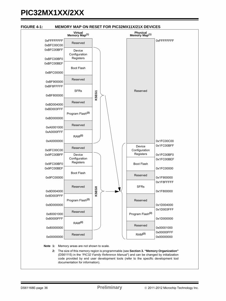
PIC32MX1XX/2XX
FIGURE 4-1: MEMORY MAP ON RESET FOR PIC32MX11X/21X DEVICES
VirtualMemory Map(1)
Physical Memory Map(1)
0xFFFFFFFFReserved
Reserved
0xFFFFFFFF
0xBFC00C00
0xBFC00BFF Device Configuration
Registers0xBFC00BF0
0xBFC00BEF
Boot Flash
0xBFC00000
Reserved0xBF900000
0xBF8FFFFF
SFRs
0xBF800000
Reserved0xBD004000
0xBD003FFF
Program Flash(2)
0xBD000000
Reserved0xA0001000
0xA0000FFF
RAM(2)
0xA0000000 0x1FC00C00
Reserved DeviceConfiguration
Registers
0x1FC00BFF
0x9FC00C00
0x9FC00BFF DeviceConfiguration
Registers
0x1FC00BF0
Boot Flash
0x1FC00BEF
0x9FC00BF0
0x9FC00BEF
Boot Flash
0x1FC00000
Reserved0x9FC00000 0x1F900000
Reserved SFRs
0x1F8FFFFF
0x9D004000 0x1F800000
0x9D003FFF
Program Flash(2) Reserved
0x9D000000 0x1D004000
ReservedProgram Flash(2)
0x1D003FFF
0x80001000
0x80000FFF
RAM(2)0x1D000000
Reserved0x80000000 0x00001000
Reserved RAM(2) 0x00000FFF
0x00000000 0x00000000
Note 1: Memory areas are not shown to scale.
2: The size of this memory region is programmable (see Section 3. “Memory Organization”(DS61115) in the “PIC32 Family Reference Manual”) and can be changed by initializationcode provided by end user development tools (refer to the specific development tooldocumentation for information).
KS
EG
1K
SE
G0
DS61168E-page 36 Preliminary 2011-2012 Microchip Technology Inc.
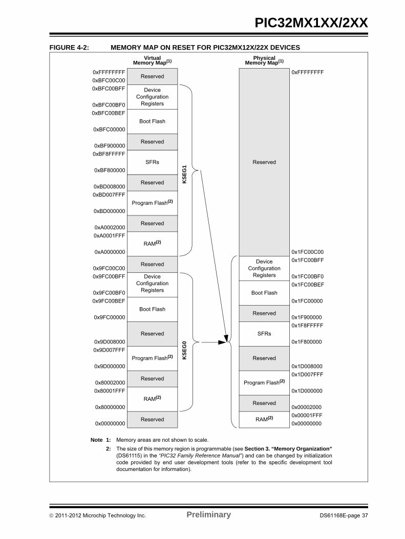
PIC32MX1XX/2XX
FIGURE 4-2: MEMORY MAP ON RESET FOR PIC32MX12X/22X DEVICES
VirtualMemory Map(1)
Physical Memory Map(1)
0xFFFFFFFFReserved
Reserved
0xFFFFFFFF
0xBFC00C00
0xBFC00BFF Device Configuration
Registers0xBFC00BF0
0xBFC00BEF
Boot Flash
0xBFC00000
Reserved0xBF900000
0xBF8FFFFF
SFRs
0xBF800000
Reserved0xBD008000
0xBD007FFF
Program Flash(2)
0xBD000000
Reserved0xA0002000
0xA0001FFF
RAM(2)
0xA0000000 0x1FC00C00
Reserved DeviceConfiguration
Registers
0x1FC00BFF
0x9FC00C00
0x9FC00BFF DeviceConfiguration
Registers
0x1FC00BF0
Boot Flash
0x1FC00BEF
0x9FC00BF0
0x9FC00BEF
Boot Flash
0x1FC00000
Reserved0x9FC00000 0x1F900000
Reserved SFRs
0x1F8FFFFF
0x9D008000 0x1F800000
0x9D007FFF
Program Flash(2) Reserved
0x9D000000 0x1D008000
ReservedProgram Flash(2)
0x1D007FFF
0x80002000
0x80001FFF
RAM(2)0x1D000000
Reserved0x80000000 0x00002000
Reserved RAM(2) 0x00001FFF
0x00000000 0x00000000
Note 1: Memory areas are not shown to scale.
2: The size of this memory region is programmable (see Section 3. “Memory Organization”(DS61115) in the “PIC32 Family Reference Manual”) and can be changed by initializationcode provided by end user development tools (refer to the specific development tooldocumentation for information).
KS
EG
1K
SE
G0
2011-2012 Microchip Technology Inc. Preliminary DS61168E-page 37

PIC32MX1XX/2XX
FIGURE 4-3: MEMORY MAP ON RESET FOR PIC32MX13X/23X DEVICES
VirtualMemory Map(1)
Physical Memory Map(1)
0xFFFFFFFFReserved
Reserved
0xFFFFFFFF
0xBFC00C00
0xBFC00BFF Device Configuration
Registers0xBFC00BF0
0xBFC00BEF
Boot Flash
0xBFC00000
Reserved0xBF900000
0xBF8FFFFF
SFRs
0xBF800000
Reserved0xBD010000
0xBD00FFFF
Program Flash(2)
0xBD000000
Reserved0xA0004000
0xA0003FFF
RAM(2)
0xA0000000 0x1FC00C00
Reserved DeviceConfiguration
Registers
0x1FC00BFF
0x9FC00C00
0x9FC00BFF DeviceConfiguration
Registers
0x1FC00BF0
Boot Flash
0x1FC00BEF
0x9FC00BF0
0x9FC00BEF
Boot Flash
0x1FC00000
Reserved0x9FC00000 0x1F900000
Reserved SFRs
0x1F8FFFFF
0x9D010000 0x1F800000
0x9D00FFFF
Program Flash(2) Reserved
0x9D000000 0x1D010000
ReservedProgram Flash(2)
0x1D00FFFF
0x80004000
0x80003FFF
RAM(2)0x1D000000
Reserved0x80000000 0x00004000
Reserved RAM(2) 0x00003FFF
0x00000000 0x00000000
Note 1: Memory areas are not shown to scale.
2: The size of this memory region is programmable (see Section 3. “Memory Organization”(DS61115) in the “PIC32 Family Reference Manual”) and can be changed by initializationcode provided by end user development tools (refer to the specific development tooldocumentation for information).
KS
EG
1K
SE
G0
DS61168E-page 38 Preliminary 2011-2012 Microchip Technology Inc.
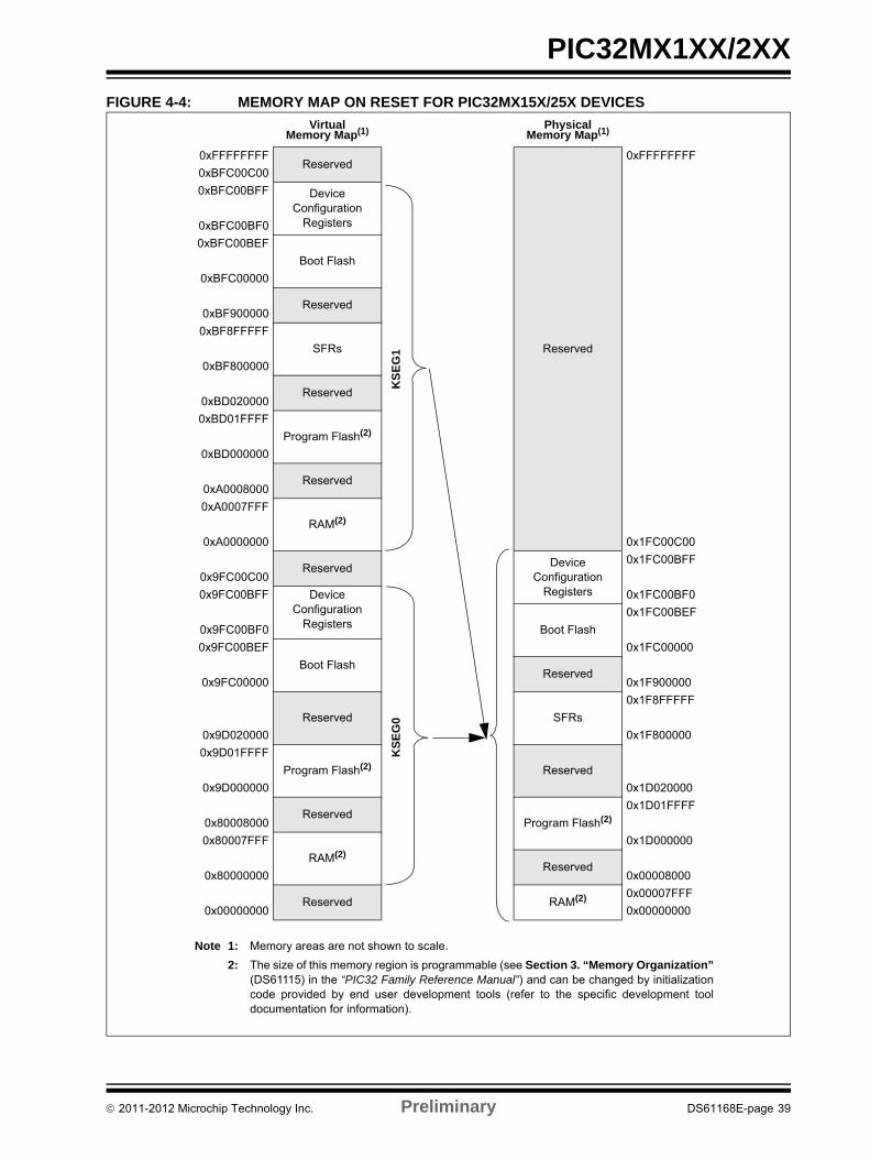
PIC32MX1XX/2XX
FIGURE 4-4: MEMORY MAP ON RESET FOR PIC32MX15X/25X DEVICES
VirtualMemory Map(1)
Physical Memory Map(1)
0xFFFFFFFFReserved
Reserved
0xFFFFFFFF
0xBFC00C00
0xBFC00BFF Device Configuration
Registers0xBFC00BF0
0xBFC00BEF
Boot Flash
0xBFC00000
Reserved0xBF900000
0xBF8FFFFF
SFRs
0xBF800000
Reserved0xBD020000
0xBD01FFFF
Program Flash(2)
0xBD000000
Reserved0xA0008000
0xA0007FFF
RAM(2)
0xA0000000 0x1FC00C00
Reserved DeviceConfiguration
Registers
0x1FC00BFF
0x9FC00C00
0x9FC00BFF DeviceConfiguration
Registers
0x1FC00BF0
Boot Flash
0x1FC00BEF
0x9FC00BF0
0x9FC00BEF
Boot Flash
0x1FC00000
Reserved0x9FC00000 0x1F900000
Reserved SFRs
0x1F8FFFFF
0x9D020000 0x1F800000
0x9D01FFFF
Program Flash(2) Reserved
0x9D000000 0x1D020000
ReservedProgram Flash(2)
0x1D01FFFF
0x80008000
0x80007FFF
RAM(2)0x1D000000
Reserved0x80000000 0x00008000
Reserved RAM(2) 0x00007FFF
0x00000000 0x00000000
Note 1: Memory areas are not shown to scale.
2: The size of this memory region is programmable (see Section 3. “Memory Organization”(DS61115) in the “PIC32 Family Reference Manual”) and can be changed by initializationcode provided by end user development tools (refer to the specific development tooldocumentation for information).
KS
EG
1K
SE
G0
2011-2012 Microchip Technology Inc. Preliminary DS61168E-page 39
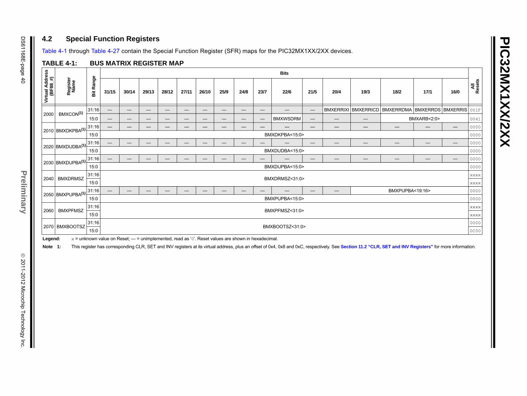
PIC
32MX
1XX
/2XX
DS
61168E-page 40
Prelim
ina
ry
2011-2012 Microchip T
echnology Inc.
All
Res
ets
19/3 18/2 17/1 16/0
MXERRICD BMXERRDMA BMXERRDS BMXERRIS 001F
— BMXARB<2:0> 0041
— — — — 0000
0000
— — — — 0000
0000
— — — — 0000
0000
xxxx
xxxx
BMXPUPBA<19:16> 0000
0000
xxxx
xxxx
0000
0C00
n 11.2 “CLR, SET and INV Registers” for more information.
4.2 Special Function Registers
Table 4-1 through Table 4-27 contain the Special Function Register (SFR) maps for the PIC32MX1XX/2XX devices. TABLE 4-1: BUS MATRIX REGISTER MAP
Vir
tual
Ad
dre
ss(B
F88
_#)
Reg
iste
rN
ame
Bit
Ran
ge
Bits
31/15 30/14 29/13 28/12 27/11 26/10 25/9 24/8 23/7 22/6 21/5 20/4
2000 BMXCON(1)31:16 — — — — — — — — — — — BMXERRIXI B
15:0 — — — — — — — — — BMXWSDRM — —
2010 BMXDKPBA(1)31:16 — — — — — — — — — — — —
15:0 BMXDKPBA<15:0>
2020 BMXDUDBA(1)31:16 — — — — — — — — — — — —
15:0 BMXDUDBA<15:0>
2030 BMXDUPBA(1)31:16 — — — — — — — — — — — —
15:0 BMXDUPBA<15:0>
2040 BMXDRMSZ31:16
BMXDRMSZ<31:0>15:0
2050 BMXPUPBA(1)31:16 — — — — — — — — — — — —
15:0 BMXPUPBA<15:0>
2060 BMXPFMSZ31:16
BMXPFMSZ<31:0>15:0
2070 BMXBOOTSZ31:16
BMXBOOTSZ<31:0>15:0
Legend: x = unknown value on Reset; — = unimplemented, read as ‘0’. Reset values are shown in hexadecimal.
Note 1: This register has corresponding CLR, SET and INV registers at its virtual address, plus an offset of 0x4, 0x8 and 0xC, respectively. See Sectio
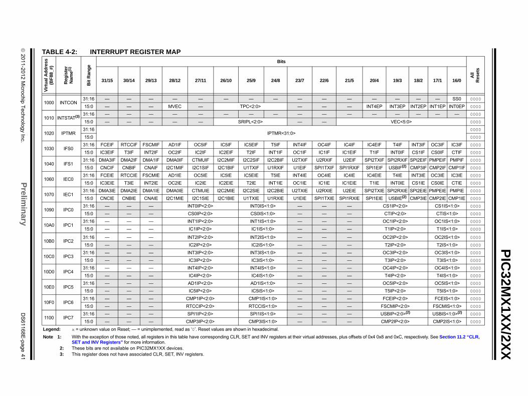
2011
-2012 Microchip T
echnology Inc.
Prelim
ina
ryD
S61168E
-page 41
PIC
32MX
1XX
/2XX
T
All
Res
ets
20/4 19/3 18/2 17/1 16/0
— — — — SS0 0000
NT4EP INT3EP INT2EP INT1EP INT0EP 0000
— — — — — 0000
VEC<5:0> 0000
0000
0000
IC4EIF T4IF INT3IF OC3IF IC3IF 0000
T1IF INT0IF CS1IF CS0IF CTIF 0000
PI2TXIF SPI2RXIF SPI2EIF PMPEIF PMPIF 0000
PI1EIF USBIF(2) CMP3IF CMP2IF CMP1IF 0000
IC4EIE T4IE INT3IE OC3IE IC3IE 0000
T1IE INT0IE CS1IE CS0IE CTIE 0000
PI2TXIE SPI2RXIE SPI2EIE PMPEIE PMPIE 0000
PI1EIE USBIE(2) CMP3IE CMP2IE CMP1IE 0000
CS1IP<2:0> CS1IS<1:0> 0000
CTIP<2:0> CTIS<1:0> 0000
OC1IP<2:0> OC1IS<1:0> 0000
T1IP<2:0> T1IS<1:0> 0000
OC2IP<2:0> OC2IS<1:0> 0000
T2IP<2:0> T2IS<1:0> 0000
OC3IP<2:0> OC3IS<1:0> 0000
T3IP<2:0> T3IS<1:0> 0000
OC4IP<2:0> OC4IS<1:0> 0000
T4IP<2:0> T4IS<1:0> 0000
OC5IP<2:0> OC5IS<1:0> 0000
T5IP<2:0> T5IS<1:0> 0000
FCEIP<2:0> FCEIS<1:0> 0000
FSCMIP<2:0> FSCMIS<1:0> 0000
USBIP<2:0>(2) USBIS<1:0>(2) 0000
CMP2IP<2:0> CMP2IS<1:0> 0000
0x4 0x8 and 0xC, respectively. See Section 11.2 “CLR,
ABLE 4-2: INTERRUPT REGISTER MAPV
irtu
al A
dd
ress
(BF
88_#
)
Reg
iste
rN
ame(1
)
Bit
Ran
ge
Bits
31/15 30/14 29/13 28/12 27/11 26/10 25/9 24/8 23/7 22/6 21/5
1000 INTCON31:16 — — — — — — — — — — —
15:0 — — — MVEC — TPC<2:0> — — — I
1010 INTSTAT(3) 31:16 — — — — — — — — — — —
15:0 — — — — — SRIPL<2:0> — —
1020 IPTMR31:16
IPTMR<31:0>15:0
1030 IFS031:16 FCEIF RTCCIF FSCMIF AD1IF OC5IF IC5IF IC5EIF T5IF INT4IF OC4IF IC4IF
15:0 IC3EIF T3IF INT2IF OC2IF IC2IF IC2EIF T2IF INT1IF OC1IF IC1IF IC1EIF
1040 IFS131:16 DMA3IF DMA2IF DMA1IF DMA0IF CTMUIF I2C2MIF I2C2SIF I2C2BIF U2TXIF U2RXIF U2EIF S
15:0 CNCIF CNBIF CNAIF I2C1MIF I2C1SIF I2C1BIF U1TXIF U1RXIF U1EIF SPI1TXIF SPI1RXIF S
1060 IEC031:16 FCEIE RTCCIE FSCMIE AD1IE OC5IE IC5IE IC5EIE T5IE INT4IE OC4IE IC4IE
15:0 IC3EIE T3IE INT2IE OC2IE IC2IE IC2EIE T2IE INT1IE OC1IE IC1IE IC1EIE
1070 IEC131:16 DMA3IE DMA2IE DMA1IE DMA0IE CTMUIE I2C2MIE I2C2SIE I2C2BIE U2TXIE U2RXIE U2EIE S
15:0 CNCIE CNBIE CNAIE I2C1MIE I2C1SIE I2C1BIE U1TXIE U1RXIE U1EIE SPI1TXIE SPI1RXIE S
1090 IPC031:16 — — — INT0IP<2:0> INT0IS<1:0> — — —
15:0 — — — CS0IP<2:0> CS0IS<1:0> — — —
10A0 IPC131:16 — — — INT1IP<2:0> INT1IS<1:0> — — —
15:0 — — — IC1IP<2:0> IC1IS<1:0> — — —
10B0 IPC231:16 — — — INT2IP<2:0> INT2IS<1:0> — — —
15:0 — — — IC2IP<2:0> IC2IS<1:0> — — —
10C0 IPC331:16 — — — INT3IP<2:0> INT3IS<1:0> — — —
15:0 — — — IC3IP<2:0> IC3IS<1:0> — — —
10D0 IPC431:16 — — — INT4IP<2:0> INT4IS<1:0> — — —
15:0 — — — IC4IP<2:0> IC4IS<1:0> — — —
10E0 IPC531:16 — — — AD1IP<2:0> AD1IS<1:0> — — —
15:0 — — — IC5IP<2:0> IC5IS<1:0> — — —
10F0 IPC631:16 — — — CMP1IP<2:0> CMP1IS<1:0> — — —
15:0 — — — RTCCIP<2:0> RTCCIS<1:0> — — —
1100 IPC731:16 — — — SPI1IP<2:0> SPI1IS<1:0> — — —
15:0 — — — CMP3IP<2:0> CMP3IS<1:0> — — —
Legend: x = unknown value on Reset; — = unimplemented, read as ‘0’. Reset values are shown in hexadecimal.
Note 1: With the exception of those noted, all registers in this table have corresponding CLR, SET and INV registers at their virtual addresses, plus offsets of SET and INV Registers” for more information.
2: These bits are not available on PIC32MX1XX devices.3: This register does not have associated CLR, SET, INV registers.
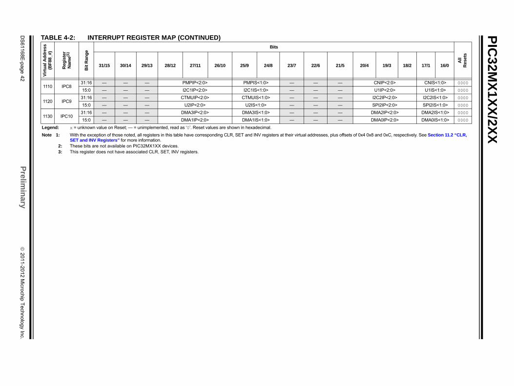
PIC
32MX
1XX
/2XX
DS
61168E-page 42
Prelim
ina
ry
2011-2012 Microchip T
echnology Inc.
CNIP<2:0> CNIS<1:0> 0000
U1IP<2:0> U1IS<1:0> 0000
I2C2IP<2:0> I2C2IS<1:0> 0000
SPI2IP<2:0> SPI2IS<1:0> 0000
DMA2IP<2:0> DMA2IS<1:0> 0000
DMA0IP<2:0> DMA0IS<1:0> 0000
All
Res
ets
20/4 19/3 18/2 17/1 16/0
ets of 0x4 0x8 and 0xC, respectively. See Section 11.2 “CLR,
1110 IPC831:16 — — — PMPIP<2:0> PMPIS<1:0> — — —
15:0 — — — I2C1IP<2:0> I2C1IS<1:0> — — —
1120 IPC931:16 — — — CTMUIP<2:0> CTMUIS<1:0> — — —
15:0 — — — U2IP<2:0> U2IS<1:0> — — —
1130 IPC1031:16 — — — DMA3IP<2:0> DMA3IS<1:0> — — —
15:0 — — — DMA1IP<2:0> DMA1IS<1:0> — — —
TABLE 4-2: INTERRUPT REGISTER MAP (CONTINUED)V
irtu
al A
dd
ress
(BF
88_#
)
Reg
iste
rN
ame(1
)
Bit
Ran
ge
Bits
31/15 30/14 29/13 28/12 27/11 26/10 25/9 24/8 23/7 22/6 21/5
Legend: x = unknown value on Reset; — = unimplemented, read as ‘0’. Reset values are shown in hexadecimal.
Note 1: With the exception of those noted, all registers in this table have corresponding CLR, SET and INV registers at their virtual addresses, plus offsSET and INV Registers” for more information.
2: These bits are not available on PIC32MX1XX devices.3: This register does not have associated CLR, SET, INV registers.
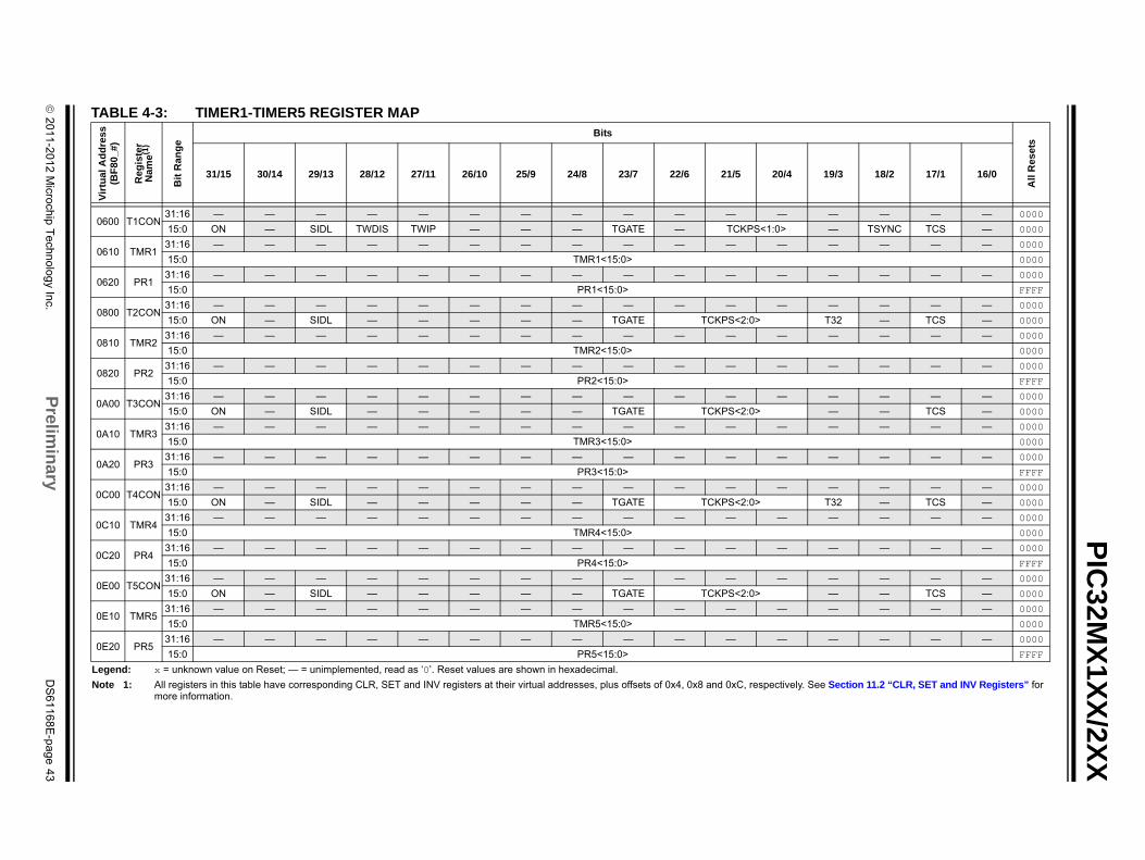
2011
-2012 Microchip T
echnology Inc.
Prelim
ina
ryD
S61168E
-page 43
PIC
32MX
1XX
/2XX
T
All
Res
ets
19/3 18/2 17/1 16/0
— — — — 0000
— TSYNC TCS — 0000
— — — — 0000
0000
— — — — 0000
FFFF
— — — — 0000
T32 — TCS — 0000
— — — — 0000
0000
— — — — 0000
FFFF
— — — — 0000
— — TCS — 0000
— — — — 0000
0000
— — — — 0000
FFFF
— — — — 0000
T32 — TCS — 0000
— — — — 0000
0000
— — — — 0000
FFFF
— — — — 0000
— — TCS — 0000
— — — — 0000
0000
— — — — 0000
FFFF
L
N ly. See Section 11.2 “CLR, SET and INV Registers” for
ABLE 4-3: TIMER1-TIMER5 REGISTER MAPV
irtu
al A
dd
ress
(BF
80
_#)
Re
gis
ter
Nam
e(1
)
Bit
Ra
ng
e
Bits
31/15 30/14 29/13 28/12 27/11 26/10 25/9 24/8 23/7 22/6 21/5 20/4
0600 T1CON31:16 — — — — — — — — — — — —
15:0 ON — SIDL TWDIS TWIP — — — TGATE — TCKPS<1:0>
0610 TMR131:16 — — — — — — — — — — — —
15:0 TMR1<15:0>
0620 PR131:16 — — — — — — — — — — — —
15:0 PR1<15:0>
0800 T2CON31:16 — — — — — — — — — — — —
15:0 ON — SIDL — — — — — TGATE TCKPS<2:0>
0810 TMR231:16 — — — — — — — — — — — —
15:0 TMR2<15:0>
0820 PR231:16 — — — — — — — — — — — —
15:0 PR2<15:0>
0A00 T3CON31:16 — — — — — — — — — — — —
15:0 ON — SIDL — — — — — TGATE TCKPS<2:0>
0A10 TMR331:16 — — — — — — — — — — — —
15:0 TMR3<15:0>
0A20 PR331:16 — — — — — — — — — — — —
15:0 PR3<15:0>
0C00 T4CON31:16 — — — — — — — — — — — —
15:0 ON — SIDL — — — — — TGATE TCKPS<2:0>
0C10 TMR431:16 — — — — — — — — — — — —
15:0 TMR4<15:0>
0C20 PR431:16 — — — — — — — — — — — —
15:0 PR4<15:0>
0E00 T5CON31:16 — — — — — — — — — — — —
15:0 ON — SIDL — — — — — TGATE TCKPS<2:0>
0E10 TMR531:16 — — — — — — — — — — — —
15:0 TMR5<15:0>
0E20 PR531:16 — — — — — — — — — — — —
15:0 PR5<15:0>
egend: x = unknown value on Reset; — = unimplemented, read as ‘0’. Reset values are shown in hexadecimal.
ote 1: All registers in this table have corresponding CLR, SET and INV registers at their virtual addresses, plus offsets of 0x4, 0x8 and 0xC, respectivemore information.
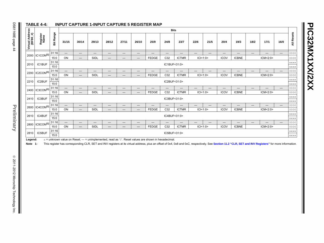
PIC
32MX
1XX
/2XX
DS
61168E-page 44
Prelim
ina
ry
2011-2012 Microchip T
echnology Inc.
All
Res
ets
20/4 19/3 18/2 17/1 16/0
— — — — — 0000
ICOV ICBNE ICM<2:0> 0000
xxxx
xxxx
— — — — — 0000
ICOV ICBNE ICM<2:0> 0000
xxxx
xxxx
— — — — — 0000
ICOV ICBNE ICM<2:0> 0000
xxxx
xxxx
— — — — — 0000
ICOV ICBNE ICM<2:0> 0000
xxxx
xxxx
— — — — — 0000
ICOV ICBNE ICM<2:0> 0000
xxxx
xxxx
tion 11.2 “CLR, SET and INV Registers” for more information.
TABLE 4-4: INPUT CAPTURE 1-INPUT CAPTURE 5 REGISTER MAPV
irtu
al A
dd
ress
(BF
80
_#)
Re
gis
ter
Nam
e
Bit
Ra
ng
e
Bits
31/15 30/14 29/13 28/12 27/11 26/10 25/9 24/8 23/7 22/6 21/5
2000 IC1CON(1)31:16 — — — — — — — — — — —
15:0 ON — SIDL — — — FEDGE C32 ICTMR ICI<1:0>
2010 IC1BUF31:16
IC1BUF<31:0>15:0
2200 IC2CON(1) 31:16 — — — — — — — — — — —
15:0 ON — SIDL — — — FEDGE C32 ICTMR ICI<1:0>
2210 IC2BUF31:16
IC2BUF<31:0>15:0
2400 IC3CON(1) 31:16 — — — — — — — — — — —
15:0 ON — SIDL — — — FEDGE C32 ICTMR ICI<1:0>
2410 IC3BUF31:16
IC3BUF<31:0>15:0
2600 IC4CON(1) 31:16 — — — — — — — — — — —
15:0 ON — SIDL — — — FEDGE C32 ICTMR ICI<1:0>
2610 IC4BUF31:16
IC4BUF<31:0>15:0
2800 IC5CON(1) 31:16 — — — — — — — — — — —
15:0 ON — SIDL — — — FEDGE C32 ICTMR ICI<1:0>
2810 IC5BUF31:16
IC5BUF<31:0>15:0
Legend: x = unknown value on Reset; — = unimplemented, read as ‘0’. Reset values are shown in hexadecimal.
Note 1: This register has corresponding CLR, SET and INV registers at its virtual address, plus an offset of 0x4, 0x8 and 0xC, respectively. See Sec
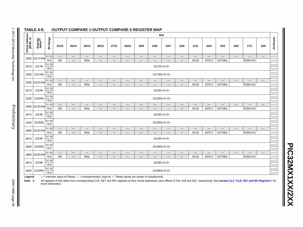
2011
-2012 Microchip T
echnology Inc.
Prelim
ina
ryD
S61168E
-page 45
PIC
32MX
1XX
/2XX
T
All
Res
ets
19/3 18/2 17/1 16/0
— — — — 0000
T OCTSEL OCM<2:0> 0000
xxxx
xxxx
xxxx
xxxx
— — — — 0000
T OCTSEL OCM<2:0> 0000
xxxx
xxxx
xxxx
xxxx
— — — — 0000
T OCTSEL OCM<2:0> 0000
xxxx
xxxx
xxxx
xxxx
— — — — 0000
T OCTSEL OCM<2:0> 0000
xxxx
xxxx
xxxx
xxxx
— — — — 0000
T OCTSEL OCM<2:0> 0000
xxxx
xxxx
xxxx
xxxx
L
N ly. See Section 11.2 “CLR, SET and INV Registers” for
ABLE 4-5: OUTPUT COMPARE 1-OUTPUT COMPARE 5 REGISTER MAPV
irtu
al A
dd
ress
(BF
80
_#)
Re
gis
ter
Nam
e(1
)
Bit
Ra
ng
e
Bits
31/15 30/14 29/13 28/12 27/11 26/10 25/9 24/8 23/7 22/6 21/5 20/4
3000 OC1CON31:16 — — — — — — — — — — — —
15:0 ON — SIDL — — — — — — — OC32 OCFL
3010 OC1R31:16
OC1R<31:0>15:0
3020 OC1RS31:16
OC1RS<31:0>15:0
3200 OC2CON31:16 — — — — — — — — — — — —
15:0 ON — SIDL — — — — — — — OC32 OCFL
3210 OC2R31:16
OC2R<31:0>15:0
3220 OC2RS31:16
OC2RS<31:0>15:0
3400 OC3CON31:16 — — — — — — — — — — — —
15:0 ON — SIDL — — — — — — — OC32 OCFL
3410 OC3R31:16
OC3R<31:0>15:0
3420 OC3RS31:1615:0
OC3RS<31:0>
3600 OC4CON31:16 — — — — — — — — — — — —
15:0 ON — SIDL — — — — — — — OC32 OCFL
3610 OC4R31:16
OC4R<31:0>15:0
3620 OC4RS31:1615:0
OC4RS<31:0>
3800 OC5CON31:16 — — — — — — — — — — — —
15:0 ON — SIDL — — — — — — — OC32 OCFL
3810 OC5R31:16
OC5R<31:0>15:0
3820 OC5RS31:16
OC5RS<31:0>15:0
egend: x = unknown value on Reset; — = unimplemented, read as ‘0’. Reset values are shown in hexadecimal.
ote 1: All registers in this table have corresponding CLR, SET and INV registers at their virtual addresses, plus offsets of 0x4, 0x8 and 0xC, respectivemore information.
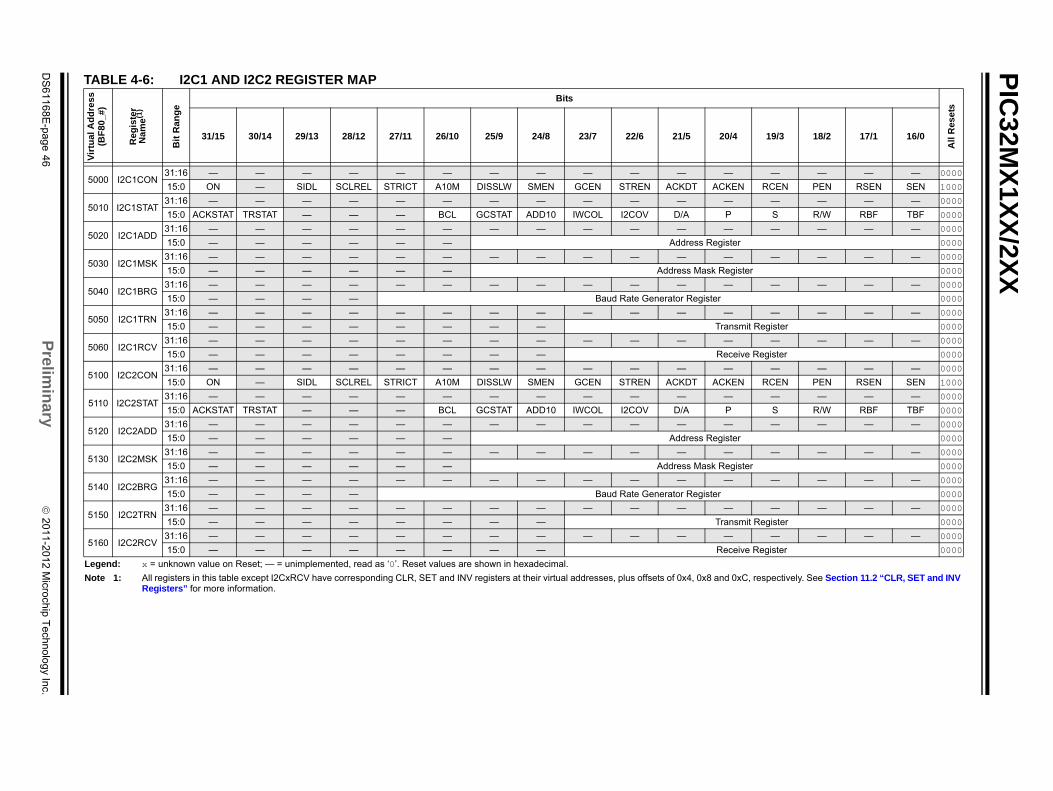
PIC
32MX
1XX
/2XX
DS
61168E-page 46
Prelim
ina
ry
2011-2012 Microchip T
echnology Inc.
All
Res
ets
20/4 19/3 18/2 17/1 16/0
— — — — — 0000
ACKEN RCEN PEN RSEN SEN 1000
— — — — — 0000
P S R/W RBF TBF 0000
— — — — — 0000
egister 0000
— — — — — 0000
k Register 0000
— — — — — 0000
ter 0000
— — — — — 0000
Transmit Register 0000
— — — — — 0000
Receive Register 0000
— — — — — 0000
ACKEN RCEN PEN RSEN SEN 1000
— — — — — 0000
P S R/W RBF TBF 0000
— — — — — 0000
egister 0000
— — — — — 0000
k Register 0000
— — — — — 0000
ter 0000
— — — — — 0000
Transmit Register 0000
— — — — — 0000
Receive Register 0000
and 0xC, respectively. See Section 11.2 “CLR, SET and INV
TABLE 4-6: I2C1 AND I2C2 REGISTER MAPV
irtu
al A
dd
ress
(BF
80
_#)
Re
gis
ter
Nam
e(1
)
Bit
Ra
ng
e
Bits
31/15 30/14 29/13 28/12 27/11 26/10 25/9 24/8 23/7 22/6 21/5
5000 I2C1CON31:16 — — — — — — — — — — —
15:0 ON — SIDL SCLREL STRICT A10M DISSLW SMEN GCEN STREN ACKDT
5010 I2C1STAT31:16 — — — — — — — — — — —
15:0 ACKSTAT TRSTAT — — — BCL GCSTAT ADD10 IWCOL I2COV D/A
5020 I2C1ADD31:16 — — — — — — — — — — —
15:0 — — — — — — Address R
5030 I2C1MSK31:16 — — — — — — — — — — —
15:0 — — — — — — Address Mas
5040 I2C1BRG31:16 — — — — — — — — — — —
15:0 — — — — Baud Rate Generator Regis
5050 I2C1TRN31:16 — — — — — — — — — — —
15:0 — — — — — — — —
5060 I2C1RCV31:16 — — — — — — — — — — —
15:0 — — — — — — — —
5100 I2C2CON31:16 — — — — — — — — — — —
15:0 ON — SIDL SCLREL STRICT A10M DISSLW SMEN GCEN STREN ACKDT
5110 I2C2STAT31:16 — — — — — — — — — — —
15:0 ACKSTAT TRSTAT — — — BCL GCSTAT ADD10 IWCOL I2COV D/A
5120 I2C2ADD31:16 — — — — — — — — — — —
15:0 — — — — — — Address R
5130 I2C2MSK31:16 — — — — — — — — — — —
15:0 — — — — — — Address Mas
5140 I2C2BRG31:16 — — — — — — — — — — —
15:0 — — — — Baud Rate Generator Regis
5150 I2C2TRN31:16 — — — — — — — — — — —
15:0 — — — — — — — —
5160 I2C2RCV31:16 — — — — — — — — — — —
15:0 — — — — — — — —
Legend: x = unknown value on Reset; — = unimplemented, read as ‘0’. Reset values are shown in hexadecimal.
Note 1: All registers in this table except I2CxRCV have corresponding CLR, SET and INV registers at their virtual addresses, plus offsets of 0x4, 0x8Registers” for more information.
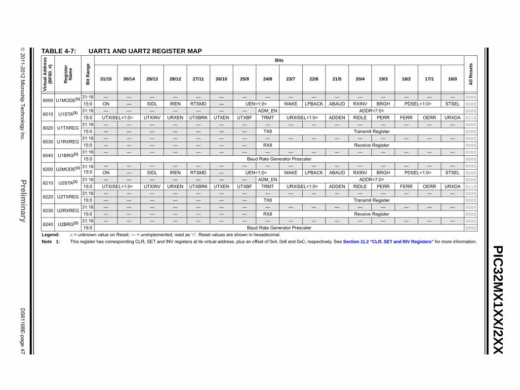
2011
-2012 Microchip T
echnology Inc.
Prelim
ina
ryD
S61168E
-page 47
PIC
32MX
1XX
/2XX
T
All
Res
ets
4 19/3 18/2 17/1 16/0
— — — — 0000
V BRGH PDSEL<1:0> STSEL 0000
DDR<7:0> 0000
LE PERR FERR OERR URXDA 0110
— — — — 0000
smit Register 0000
— — — — 0000
eive Register 0000
— — — — 0000
0000
— — — — 0000
V BRGH PDSEL<1:0> STSEL 0000
DDR<7:0> 0000
LE PERR FERR OERR URXDA 0110
— — — — 0000
smit Register 0000
— — — — 0000
eive Register 0000
— — — — 0000
0000
L
N 1.2 “CLR, SET and INV Registers” for more information.
ABLE 4-7: UART1 AND UART2 REGISTER MAPV
irtu
al A
dd
ress
(BF
80
_#)
Re
gis
ter
Nam
e
Bit
Ra
ng
e
Bits
31/15 30/14 29/13 28/12 27/11 26/10 25/9 24/8 23/7 22/6 21/5 20/
6000 U1MODE(1) 31:16 — — — — — — — — — — — —
15:0 ON — SIDL IREN RTSMD — UEN<1:0> WAKE LPBACK ABAUD RXIN
6010 U1STA(1) 31:16 — — — — — — — ADM_EN A
15:0 UTXISEL<1:0> UTXINV URXEN UTXBRK UTXEN UTXBF TRMT URXISEL<1:0> ADDEN RID
6020 U1TXREG31:16 — — — — — — — — — — — —
15:0 — — — — — — — TX8 Tran
6030 U1RXREG31:16 — — — — — — — — — — — —
15:0 — — — — — — — RX8 Rec
6040 U1BRG(1) 31:16 — — — — — — — — — — — —
15:0 Baud Rate Generator Prescaler
6200 U2MODE(1) 31:1615:0
— — — — — — — — — — — —
ON — SIDL IREN RTSMD — UEN<1:0> WAKE LPBACK ABAUD RXIN
6210 U2STA(1) 31:16 — — — — — — — ADM_EN A
15:0 UTXISEL<1:0> UTXINV URXEN UTXBRK UTXEN UTXBF TRMT URXISEL<1:0> ADDEN RID
6220 U2TXREG31:16 — — — — — — — — — — — —
15:0 — — — — — — — TX8 Tran
6230 U2RXREG31:16 — — — — — — — — — — — —
15:0 — — — — — — — RX8 Rec
6240 U2BRG(1) 31:16 — — — — — — — — — — — —
15:0 Baud Rate Generator Prescaler
egend: x = unknown value on Reset; — = unimplemented, read as ‘0’. Reset values are shown in hexadecimal.
ote 1: This register has corresponding CLR, SET and INV registers at its virtual address, plus an offset of 0x4, 0x8 and 0xC, respectively. See Section 1
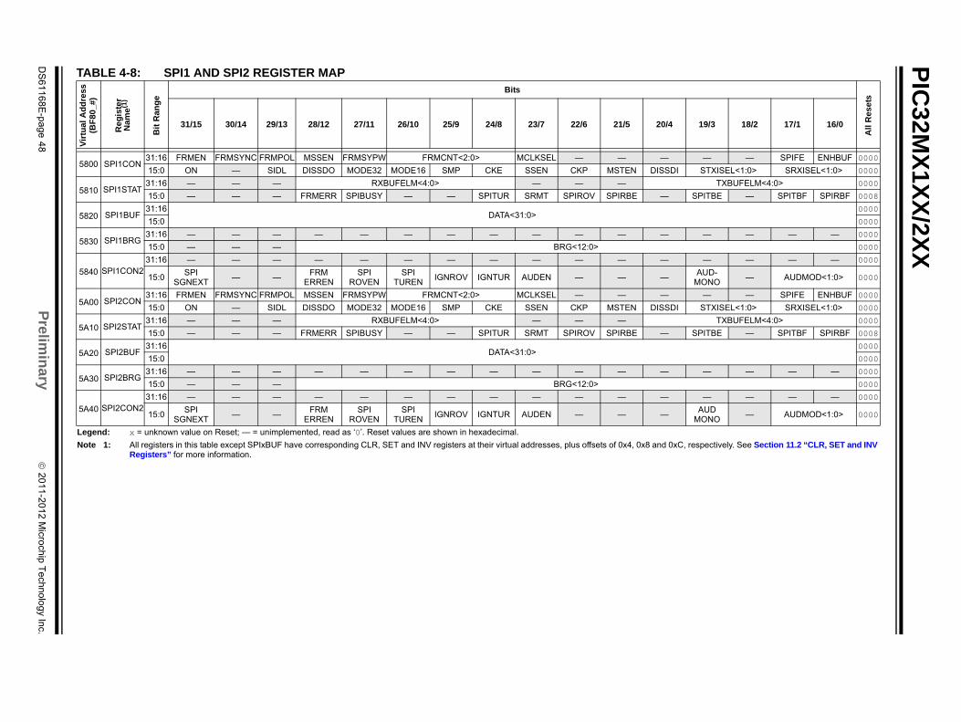
PIC
32MX
1XX
/2XX
DS
61168E-page 48
Prelim
ina
ry
2011-2012 Microchip T
echnology Inc.
All
Res
ets
20/4 19/3 18/2 17/1 16/0
— — — SPIFE ENHBUF 0000
DISSDI STXISEL<1:0> SRXISEL<1:0> 0000
TXBUFELM<4:0> 0000
— SPITBE — SPITBF SPIRBF 0008
0000
0000
— — — — — 0000
0000
— — — — — 0000
—AUD-
MONO— AUDMOD<1:0> 0000
— — — SPIFE ENHBUF 0000
DISSDI STXISEL<1:0> SRXISEL<1:0> 0000
TXBUFELM<4:0> 0000
— SPITBE — SPITBF SPIRBF 0008
0000
0000
— — — — — 0000
0000
— — — — — 0000
—AUD
MONO— AUDMOD<1:0> 0000
and 0xC, respectively. See Section 11.2 “CLR, SET and INV
TABLE 4-8: SPI1 AND SPI2 REGISTER MAPV
irtu
al A
dd
ress
(BF
80
_#)
Re
gis
ter
Nam
e(1
)
Bit
Ra
ng
e
Bits
31/15 30/14 29/13 28/12 27/11 26/10 25/9 24/8 23/7 22/6 21/5
5800 SPI1CON31:16 FRMEN FRMSYNC FRMPOL MSSEN FRMSYPW FRMCNT<2:0> MCLKSEL — —
15:0 ON — SIDL DISSDO MODE32 MODE16 SMP CKE SSEN CKP MSTEN
5810 SPI1STAT31:16 — — — RXBUFELM<4:0> — — —
15:0 — — — FRMERR SPIBUSY — — SPITUR SRMT SPIROV SPIRBE
5820 SPI1BUF31:16
DATA<31:0>15:0
5830 SPI1BRG31:16 — — — — — — — — — — —
15:0 — — — BRG<12:0>
5840 SPI1CON231:16 — — — — — — — — — — —
15:0SPI
SGNEXT— —
FRMERREN
SPIROVEN
SPITUREN
IGNROV IGNTUR AUDEN — —
5A00 SPI2CON31:16 FRMEN FRMSYNC FRMPOL MSSEN FRMSYPW FRMCNT<2:0> MCLKSEL — —
15:0 ON — SIDL DISSDO MODE32 MODE16 SMP CKE SSEN CKP MSTEN
5A10 SPI2STAT31:16 — — — RXBUFELM<4:0> — — —
15:0 — — — FRMERR SPIBUSY — — SPITUR SRMT SPIROV SPIRBE
5A20 SPI2BUF31:16
DATA<31:0>15:0
5A30 SPI2BRG31:16 — — — — — — — — — — —
15:0 — — — BRG<12:0>
5A40 SPI2CON231:16 — — — — — — — — — — —
15:0SPI
SGNEXT— —
FRMERREN
SPIROVEN
SPITUREN
IGNROV IGNTUR AUDEN — —
Legend: x = unknown value on Reset; — = unimplemented, read as ‘0’. Reset values are shown in hexadecimal.
Note 1: All registers in this table except SPIxBUF have corresponding CLR, SET and INV registers at their virtual addresses, plus offsets of 0x4, 0x8Registers” for more information.
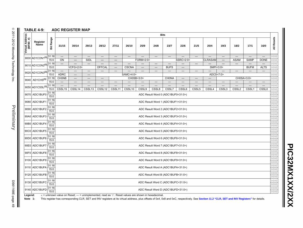
2011
-2012 Microchip T
echnology Inc.
Prelim
ina
ryD
S61168E
-page 49
PIC
32MX
1XX
/2XX
T
All
Res
ets
4 19/3 18/2 17/1 16/0
— — — — 0000SAM — ASAM SAMP DONE 0000
— — — — 0000MPI<3:0> BUFM ALTS 0000
— — — — 0000DCS<7:0> 0000
CH0SA<3:0> 0000— — — — 0000— — — — 0000
L4 CSSL3 CSSL2 CSSL1 CSSL0 0000000000000000000000000000000000000000000000000000000000000000000000000000000000000000000000000000
0000000000000000
LN .2 “CLR, SET and INV Registers” for details.
ABLE 4-9: ADC REGISTER MAPV
irtu
al A
dd
ress
(BF
80
_#)
RegisterName
Bit
Ra
ng
e
Bits
31/15 30/14 29/13 28/12 27/11 26/10 25/9 24/8 23/7 22/6 21/5 20/
9000 AD1CON1(1) 31:16 — — — — — — — — — — — —15:0 ON — SIDL — — FORM<2:0> SSRC<2:0> CLRA
9010 AD1CON2(1) 31:16 — — — — — — — — — — — —15:0 VCFG<2:0> OFFCAL — CSCNA — — BUFS — S
9020 AD1CON3(1) 31:16 — — — — — — — — — — — —15:0 ADRC — — SAMC<4:0> A
9040 AD1CHS(1) 31:16 CH0NB — — — CH0SB<3:0> CH0NA — — —15:0 — — — — — — — — — — — —
9050 AD1CSSL(1) 31:16 — — — — — — — — — — — —15:0 CSSL15 CSSL14 CSSL13 CSSL12 CSSL11 CSSL10 CSSL9 CSSL8 CSSL7 CSSL6 CSSL5 CSS
9070 ADC1BUF031:16
ADC Result Word 0 (ADC1BUF0<31:0>)15:0
9080 ADC1BUF131:16
ADC Result Word 1 (ADC1BUF1<31:0>)15:0
9090 ADC1BUF231:16
ADC Result Word 2 (ADC1BUF2<31:0>)15:0
90A0 ADC1BUF331:16
ADC Result Word 3 (ADC1BUF3<31:0>)15:0
90B0 ADC1BUF431:16
ADC Result Word 4 (ADC1BUF4<31:0>)15:0
90C0 ADC1BUF531:16
ADC Result Word 5 (ADC1BUF5<31:0>)15:0
90D0 ADC1BUF631:16
ADC Result Word 6 (ADC1BUF6<31:0>)15:0
90E0 ADC1BUF731:16
ADC Result Word 7 (ADC1BUF7<31:0>)15:0
90F0 ADC1BUF831:16
ADC Result Word 8 (ADC1BUF8<31:0>)15:0
9100 ADC1BUF931:16
ADC Result Word 9 (ADC1BUF9<31:0>)15:0
9110 ADC1BUFA31:16
ADC Result Word A (ADC1BUFA<31:0>)15:0
9120 ADC1BUFB31:16
ADC Result Word B (ADC1BUFB<31:0>)15:0
9130 ADC1BUFC31:16
ADC Result Word C (ADC1BUFC<31:0>)15:0
9140 ADC1BUFD31:16
ADC Result Word D (ADC1BUFD<31:0>)15:0
egend: x = unknown value on Reset; — = unimplemented, read as ‘0’. Reset values are shown in hexadecimal.ote 1: This register has corresponding CLR, SET and INV registers at its virtual address, plus offsets of 0x4, 0x8 and 0xC, respectively. See Section 11
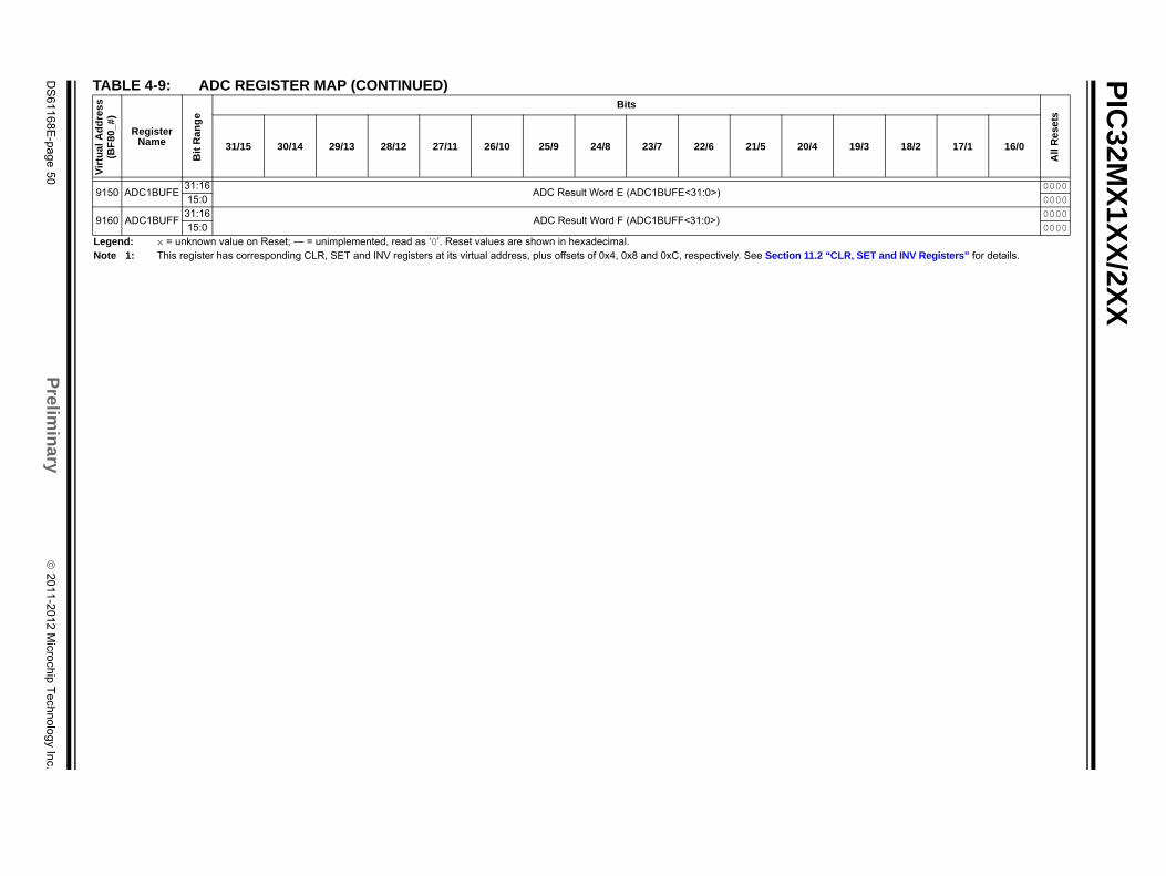
PIC
32MX
1XX
/2XX
DS
61168E-page 50
Prelim
ina
ry
2011-2012 Microchip T
echnology Inc.
0000000000000000
All
Re
sets
20/4 19/3 18/2 17/1 16/0
ion 11.2 “CLR, SET and INV Registers” for details.
9150 ADC1BUFE31:16
ADC Result Word E (ADC1BUFE<31:0>)15:0
9160 ADC1BUFF31:16
ADC Result Word F (ADC1BUFF<31:0>)15:0
TABLE 4-9: ADC REGISTER MAP (CONTINUED)V
irtu
al A
dd
res
s(B
F80
_#
)
RegisterName
Bit
Ran
ge
Bits
31/15 30/14 29/13 28/12 27/11 26/10 25/9 24/8 23/7 22/6 21/5
Legend: x = unknown value on Reset; — = unimplemented, read as ‘0’. Reset values are shown in hexadecimal.Note 1: This register has corresponding CLR, SET and INV registers at its virtual address, plus offsets of 0x4, 0x8 and 0xC, respectively. See Sect
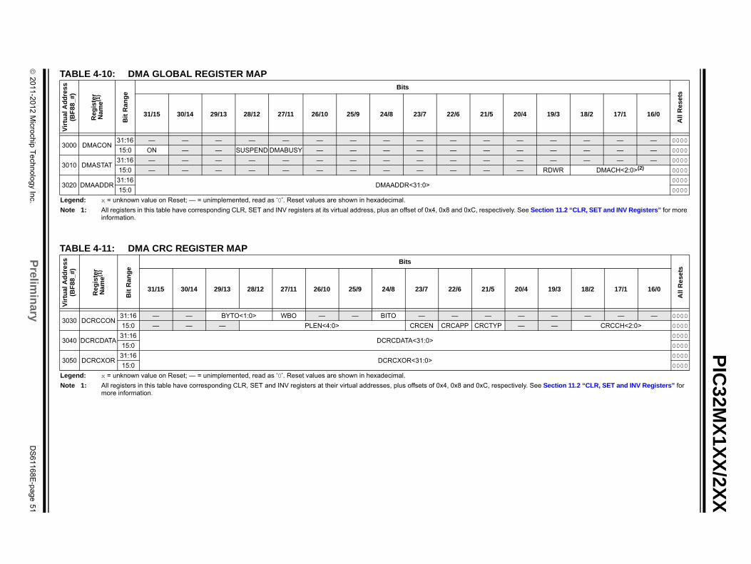
2011
-2012 Microchip T
echnology Inc.
Prelim
ina
ryD
S61168E
-page 51
PIC
32MX
1XX
/2XX
T
All
Res
ets
4 19/3 18/2 17/1 16/0
— — — — 0000
— — — — 0000
— — — — 0000
RDWR DMACH<2:0>(2) 0000
0000
0000
L
N e Section 11.2 “CLR, SET and INV Registers” for more
T
All
Re
se
ts
/4 19/3 18/2 17/1 16/0
— — — — 0000
— CRCCH<2:0> 0000
0000
0000
0000
0000
L
N ly. See Section 11.2 “CLR, SET and INV Registers” for
ABLE 4-10: DMA GLOBAL REGISTER MAPV
irtu
al A
dd
ress
(BF
88
_#)
Re
gis
ter
Nam
e(1
)
Bit
Ra
ng
e
Bits
31/15 30/14 29/13 28/12 27/11 26/10 25/9 24/8 23/7 22/6 21/5 20/
3000 DMACON31:16 — — — — — — — — — — — —
15:0 ON — — SUSPEND DMABUSY — — — — — — —
3010 DMASTAT31:16 — — — — — — — — — — — —
15:0 — — — — — — — — — — — —
3020 DMAADDR31:16
DMAADDR<31:0>15:0
egend: x = unknown value on Reset; — = unimplemented, read as ‘0’. Reset values are shown in hexadecimal.
ote 1: All registers in this table have corresponding CLR, SET and INV registers at its virtual address, plus an offset of 0x4, 0x8 and 0xC, respectively. Seinformation.
ABLE 4-11: DMA CRC REGISTER MAP
Vir
tual
Ad
dre
ss(B
F8
8_#
)
Re
gis
ter
Na
me
(1)
Bit
Ra
ng
e
Bits
31/15 30/14 29/13 28/12 27/11 26/10 25/9 24/8 23/7 22/6 21/5 20
3030 DCRCCON31:16 — — BYTO<1:0> WBO — — BITO — — — —
15:0 — — — PLEN<4:0> CRCEN CRCAPP CRCTYP —
3040 DCRCDATA31:16
DCRCDATA<31:0>15:0
3050 DCRCXOR31:16
DCRCXOR<31:0>15:0
egend: x = unknown value on Reset; — = unimplemented, read as ‘0’. Reset values are shown in hexadecimal.
ote 1: All registers in this table have corresponding CLR, SET and INV registers at their virtual addresses, plus offsets of 0x4, 0x8 and 0xC, respectivemore information.
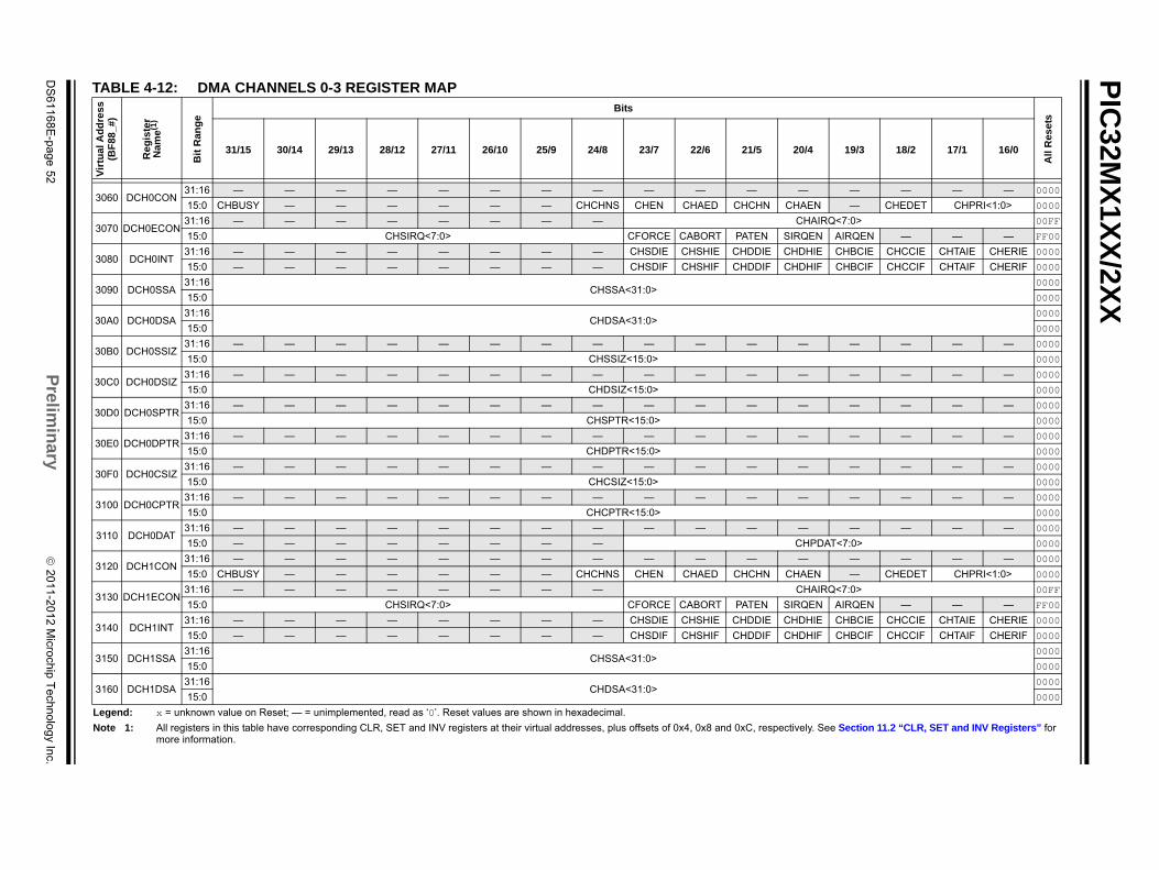
PIC
32MX
1XX
/2XX
DS
61168E-page 52
Prelim
ina
ry
2011-2012 Microchip T
echnology Inc.
All
Res
ets
20/4 19/3 18/2 17/1 16/0
— — — — — 0000
CHAEN — CHEDET CHPRI<1:0> 0000
CHAIRQ<7:0> 00FF
SIRQEN AIRQEN — — — FF00
CHDHIE CHBCIE CHCCIE CHTAIE CHERIE 0000
CHDHIF CHBCIF CHCCIF CHTAIF CHERIF 0000
0000
0000
0000
0000
— — — — — 0000
0000
— — — — — 0000
0000
— — — — — 0000
0000
— — — — — 0000
0000
— — — — — 0000
0000
— — — — — 0000
0000
— — — — — 0000
CHPDAT<7:0> 0000
— — — — — 0000
CHAEN — CHEDET CHPRI<1:0> 0000
CHAIRQ<7:0> 00FF
SIRQEN AIRQEN — — — FF00
CHDHIE CHBCIE CHCCIE CHTAIE CHERIE 0000
CHDHIF CHBCIF CHCCIF CHTAIF CHERIF 0000
0000
0000
0000
0000
ctively. See Section 11.2 “CLR, SET and INV Registers” for
TABLE 4-12: DMA CHANNELS 0-3 REGISTER MAPV
irtu
al A
dd
ress
(BF
88
_#)
Re
gis
ter
Nam
e(1
)
Bit
Ra
ng
e
Bits
31/15 30/14 29/13 28/12 27/11 26/10 25/9 24/8 23/7 22/6 21/5
3060 DCH0CON31:16 — — — — — — — — — — —
15:0 CHBUSY — — — — — — CHCHNS CHEN CHAED CHCHN
3070 DCH0ECON31:16 — — — — — — — —
15:0 CHSIRQ<7:0> CFORCE CABORT PATEN
3080 DCH0INT31:16 — — — — — — — — CHSDIE CHSHIE CHDDIE
15:0 — — — — — — — — CHSDIF CHSHIF CHDDIF
3090 DCH0SSA31:16
CHSSA<31:0>15:0
30A0 DCH0DSA31:16
CHDSA<31:0>15:0
30B0 DCH0SSIZ31:16 — — — — — — — — — — —
15:0 CHSSIZ<15:0>
30C0 DCH0DSIZ31:16 — — — — — — — — — — —
15:0 CHDSIZ<15:0>
30D0 DCH0SPTR31:16 — — — — — — — — — — —
15:0 CHSPTR<15:0>
30E0 DCH0DPTR31:16 — — — — — — — — — — —
15:0 CHDPTR<15:0>
30F0 DCH0CSIZ31:16 — — — — — — — — — — —
15:0 CHCSIZ<15:0>
3100 DCH0CPTR31:16 — — — — — — — — — — —
15:0 CHCPTR<15:0>
3110 DCH0DAT31:16 — — — — — — — — — — —
15:0 — — — — — — — —
3120 DCH1CON31:16 — — — — — — — — — — —
15:0 CHBUSY — — — — — — CHCHNS CHEN CHAED CHCHN
3130 DCH1ECON31:16 — — — — — — — —
15:0 CHSIRQ<7:0> CFORCE CABORT PATEN
3140 DCH1INT31:16 — — — — — — — — CHSDIE CHSHIE CHDDIE
15:0 — — — — — — — — CHSDIF CHSHIF CHDDIF
3150 DCH1SSA31:16
CHSSA<31:0>15:0
3160 DCH1DSA31:16
CHDSA<31:0>15:0
Legend: x = unknown value on Reset; — = unimplemented, read as ‘0’. Reset values are shown in hexadecimal.
Note 1: All registers in this table have corresponding CLR, SET and INV registers at their virtual addresses, plus offsets of 0x4, 0x8 and 0xC, respemore information.
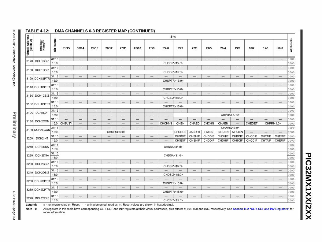
2011
-2012 Microchip T
echnology Inc.
Prelim
ina
ryD
S61168E
-page 53
PIC
32MX
1XX
/2XX
— — — — 0000
0000
— — — — 0000
0000
— — — — 0000
0000
— — — — 0000
0000
— — — — 0000
0000
— — — — 0000
0000
— — — — 0000
PDAT<7:0> 0000
— — — — 0000
EN — CHEDET CHPRI<1:0> 0000
AIRQ<7:0> 00FF
EN AIRQEN — — — FF00
HIE CHBCIE CHCCIE CHTAIE CHERIE 0000
HIF CHBCIF CHCCIF CHTAIF CHERIF 0000
0000
0000
0000
0000
— — — — 0000
0000
— — — — 0000
0000
— — — — 0000
0000
— — — — 0000
0000
— — — — 0000
0000
T
All
Re
sets
4 19/3 18/2 17/1 16/0
L
N ly. See Section 11.2 “CLR, SET and INV Registers” for
3170 DCH1SSIZ31:16 — — — — — — — — — — — —
15:0 CHSSIZ<15:0>
3180 DCH1DSIZ31:16 — — — — — — — — — — — —
15:0 CHDSIZ<15:0>
3190 DCH1SPTR31:16 — — — — — — — — — — — —
15:0 CHSPTR<15:0>
31A0 DCH1DPTR31:16 — — — — — — — — — — — —
15:0 CHDPTR<15:0>
31B0 DCH1CSIZ31:16 — — — — — — — — — — — —
15:0 CHCSIZ<15:0>
31C0 DCH1CPTR31:16 — — — — — — — — — — — —
15:0 CHCPTR<15:0>
31D0 DCH1DAT31:16 — — — — — — — — — — — —
15:0 — — — — — — — — CH
31E0 DCH2CON31:16 — — — — — — — — — — — —
15:0 CHBUSY — — — — — — CHCHNS CHEN CHAED CHCHN CHA
31F0 DCH2ECON31:16 — — — — — — — — CH
15:0 CHSIRQ<7:0> CFORCE CABORT PATEN SIRQ
3200 DCH2INT31:16 — — — — — — — — CHSDIE CHSHIE CHDDIE CHD
15:0 — — — — — — — — CHSDIF CHSHIF CHDDIF CHD
3210 DCH2SSA31:16
CHSSA<31:0>15:0
3220 DCH2DSA31:16
CHDSA<31:0>15:0
3230 DCH2SSIZ31:16 — — — — — — — — — — — —
15:0 CHSSIZ<15:0>
3240 DCH2DSIZ31:16 — — — — — — — — — — — —
15:0 CHDSIZ<15:0>
3250 DCH2SPTR31:16 — — — — — — — — — — — —
15:0 CHSPTR<15:0>
3260 DCH2DPTR31:16 — — — — — — — — — — — —
15:0 CHDPTR<15:0>
3270 DCH2CSIZ31:16 — — — — — — — — — — — —
15:0 CHCSIZ<15:0>
ABLE 4-12: DMA CHANNELS 0-3 REGISTER MAP (CONTINUED)V
irtu
al A
dd
res
s(B
F88
_#
)
Reg
iste
rN
ame
(1)
Bit
Ran
ge
Bits
31/15 30/14 29/13 28/12 27/11 26/10 25/9 24/8 23/7 22/6 21/5 20/
egend: x = unknown value on Reset; — = unimplemented, read as ‘0’. Reset values are shown in hexadecimal.
ote 1: All registers in this table have corresponding CLR, SET and INV registers at their virtual addresses, plus offsets of 0x4, 0x8 and 0xC, respectivemore information.
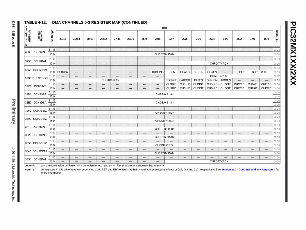
PIC
32MX
1XX
/2XX
DS
61168E-page 54
Prelim
ina
ry
2011-2012 Microchip T
echnology Inc.
— — — — — 0000
0000
— — — — — 0000
CHPDAT<7:0> 0000
— — — — — 0000
CHAEN — CHEDET CHPRI<1:0> 0000
CHAIRQ<7:0> 00FF
SIRQEN AIRQEN — — — FF00
CHDHIE CHBCIE CHCCIE CHTAIE CHERIE 0000
CHDHIF CHBCIF CHCCIF CHTAIF CHERIF 0000
0000
0000
0000
0000
— — — — — 0000
0000
— — — — — 0000
0000
— — — — — 0000
0000
— — — — — 0000
0000
— — — — — 0000
0000
— — — — — 0000
0000
— — — — — 0000
CHPDAT<7:0> 0000
All
Re
sets
20/4 19/3 18/2 17/1 16/0
ctively. See Section 11.2 “CLR, SET and INV Registers” for
3280 DCH2CPTR31:16 — — — — — — — — — — —
15:0 CHCPTR<15:0>
3290 DCH2DAT31:16 — — — — — — — — — — —
15:0 — — — — — — — —
32A0 DCH3CON31:16 — — — — — — — — — — —
15:0 CHBUSY — — — — — — CHCHNS CHEN CHAED CHCHN
32B0 DCH3ECON31:16 — — — — — — — —
15:0 CHSIRQ<7:0> CFORCE CABORT PATEN
32C0 DCH3INT31:16 — — — — — — — — CHSDIE CHSHIE CHDDIE
15:0 — — — — — — — — CHSDIF CHSHIF CHDDIF
32D0 DCH3SSA31:16
CHSSA<31:0>15:0
32E0 DCH3DSA31:16
CHDSA<31:0>15:0
32F0 DCH3SSIZ31:16 — — — — — — — — — — —
15:0 CHSSIZ<15:0>
3300 DCH3DSIZ31:16 — — — — — — — — — — —
15:0 CHDSIZ<15:0>
3310 DCH3SPTR31:16 — — — — — — — — — — —
15:0 CHSPTR<15:0>
3320 DCH3DPTR31:16 — — — — — — — — — — —
15:0 CHDPTR<15:0>
3330 DCH3CSIZ31:16 — — — — — — — — — — —
15:0 CHCSIZ<15:0>
3340 DCH3CPTR31:16 — — — — — — — — — — —
15:0 CHCPTR<15:0>
3350 DCH3DAT31:16 — — — — — — — — — — —
15:0 — — — — — — — —
TABLE 4-12: DMA CHANNELS 0-3 REGISTER MAP (CONTINUED)V
irtu
al A
dd
res
s(B
F88
_#
)
Reg
iste
rN
ame
(1)
Bit
Ran
ge
Bits
31/15 30/14 29/13 28/12 27/11 26/10 25/9 24/8 23/7 22/6 21/5
Legend: x = unknown value on Reset; — = unimplemented, read as ‘0’. Reset values are shown in hexadecimal.
Note 1: All registers in this table have corresponding CLR, SET and INV registers at their virtual addresses, plus offsets of 0x4, 0x8 and 0xC, respemore information.
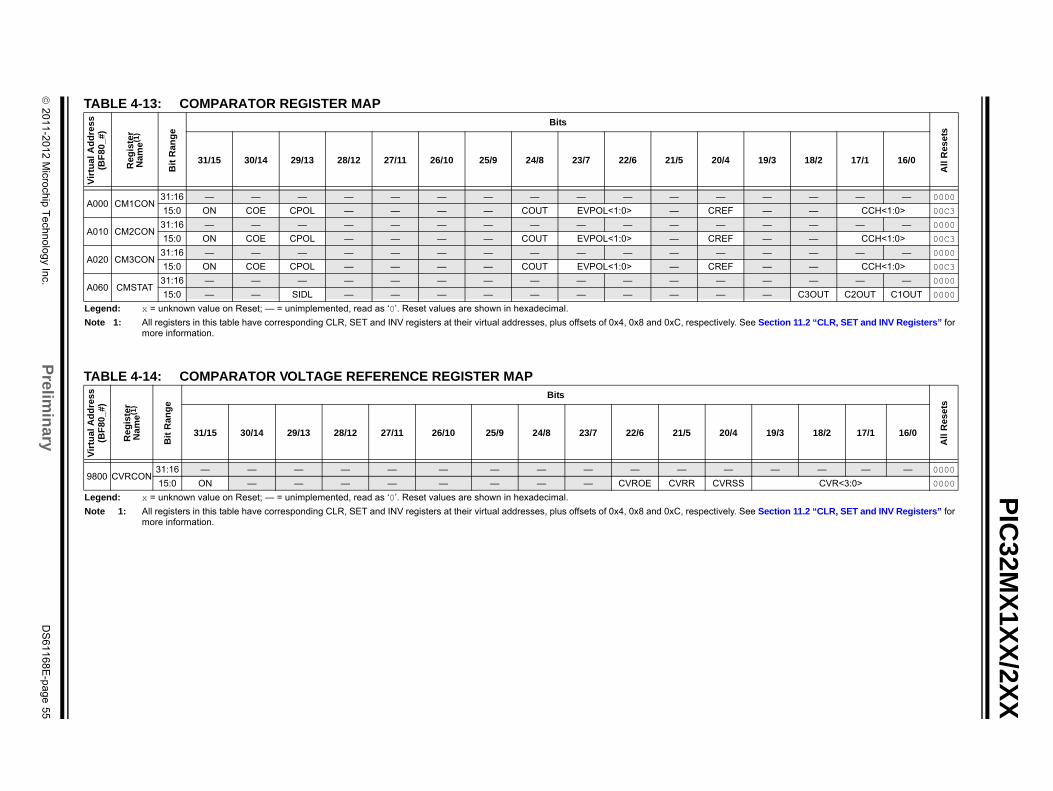
2011
-2012 Microchip T
echnology Inc.
Prelim
ina
ryD
S61168E
-page 55
PIC
32MX
1XX
/2XX
T
All
Res
ets
19/3 18/2 17/1 16/0
— — — — 0000
— — CCH<1:0> 00C3
— — — — 0000
— — CCH<1:0> 00C3
— — — — 0000
— — CCH<1:0> 00C3
— — — — 0000
— C3OUT C2OUT C1OUT 0000
L
N . See Section 11.2 “CLR, SET and INV Registers” for
T
All
Res
ets
4 19/3 18/2 17/1 16/0
— — — — 0000
SS CVR<3:0> 0000
L
N . See Section 11.2 “CLR, SET and INV Registers” for
ABLE 4-13: COMPARATOR REGISTER MAPV
irtu
al A
dd
ress
(BF
80
_#)
Re
gis
ter
Nam
e(1
)
Bit
Ra
ng
e
Bits
31/15 30/14 29/13 28/12 27/11 26/10 25/9 24/8 23/7 22/6 21/5 20/4
A000 CM1CON31:16 — — — — — — — — — — — —
15:0 ON COE CPOL — — — — COUT EVPOL<1:0> — CREF
A010 CM2CON31:16 — — — — — — — — — — — —
15:0 ON COE CPOL — — — — COUT EVPOL<1:0> — CREF
A020 CM3CON31:16 — — — — — — — — — — — —
15:0 ON COE CPOL — — — — COUT EVPOL<1:0> — CREF
A060 CMSTAT31:16 — — — — — — — — — — — —
15:0 — — SIDL — — — — — — — — —
egend: x = unknown value on Reset; — = unimplemented, read as ‘0’. Reset values are shown in hexadecimal.
ote 1: All registers in this table have corresponding CLR, SET and INV registers at their virtual addresses, plus offsets of 0x4, 0x8 and 0xC, respectivelymore information.
ABLE 4-14: COMPARATOR VOLTAGE REFERENCE REGISTER MAP
Vir
tual
Ad
dre
ss(B
F8
0_
#)
Re
gis
ter
Nam
e(1
)
Bit
Ran
ge
Bits
31/15 30/14 29/13 28/12 27/11 26/10 25/9 24/8 23/7 22/6 21/5 20/
9800 CVRCON31:16 — — — — — — — — — — — —
15:0 ON — — — — — — — — CVROE CVRR CVR
egend: x = unknown value on Reset; — = unimplemented, read as ‘0’. Reset values are shown in hexadecimal.
ote 1: All registers in this table have corresponding CLR, SET and INV registers at their virtual addresses, plus offsets of 0x4, 0x8 and 0xC, respectivelymore information.
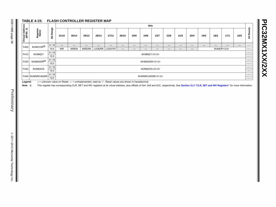
PIC
32MX
1XX
/2XX
DS
61168E-page 56
Prelim
ina
ry
2011-2012 Microchip T
echnology Inc.
All
Res
ets
20/4 19/3 18/2 17/1 16/0
— — — — — 0000
— NVMOP<3:0> 0000
0000
0000
0000
0000
0000
0000
0000
0000
ion 11.2 “CLR, SET and INV Registers” for more information.
TABLE 4-15: FLASH CONTROLLER REGISTER MAPV
irtu
al A
dd
ress
(BF
80
_#)
Re
gis
ter
Nam
e
Bit
Ra
ng
e
Bits
31/15 30/14 29/13 28/12 27/11 26/10 25/9 24/8 23/7 22/6 21/5
F400 NVMCON(1) 31:16 — — — — — — — — — — —
15:0 WR WREN WRERR LVDERR LVDSTAT — — — — — —
F410 NVMKEY31:16
NVMKEY<31:0>15:0
F420 NVMADDR(1) 31:16NVMADDR<31:0>
15:0
F430 NVMDATA31:16
NVMDATA<31:0>15:0
F440 NVMSRCADDR31:16
NVMSRCADDR<31:0>15:0
Legend: x = unknown value on Reset; — = unimplemented, read as ‘0’. Reset values are shown in hexadecimal.
Note 1: This register has corresponding CLR, SET and INV registers at its virtual address, plus offsets of 0x4, 0x8 and 0xC, respectively. See Sect
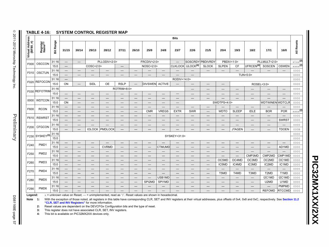
2011
-2012 Microchip T
echnology Inc.
Prelim
ina
ryD
S61168E
-page 57
PIC
32MX
1XX
/2XX
T
All
Re
se
ts
19/3 18/2 17/1 16/0
V<1:0> PLLMULT<2:0> x1xx(2)
CF UFRCEN(4) SOSCEN OSWEN xxxx(2)
— — — — 0000
TUN<5:0> 0000
0000
ROSEL<3:0> 0000
— — — — 0000
— — — — 0000
— — — — 0000
0> WDTWINEN WDTCLR 0000
— — — — 0000
SLEEP IDLE BOR POR xxxx(2)
— — — — 0000
— — — SWRST 0000
— — — — 0000
JTAGEN — — TDOEN 000B
0000
0000
— — — — 0000
— — — AD1MD 0000
— — — — 0000
— CMP3MD CMP2MD CMP1MD 0000
OC4MD OC3MD OC2MD OC1MD 0000
IC4MD IC3MD IC2MD IC1MD 0000
— — — — 0000
T4MD T3MD T2MD T1MD 0000
— — I2C1MD I2C1MD 0000
— — U2MD U1MD 0000
— — — PMPMD 0000
— — REFOMD RTCCMD 0000
L
N ts of 0x4, 0x8 and 0xC, respectively. See Section 11.2
ABLE 4-16: SYSTEM CONTROL REGISTER MAPV
irtu
al A
dd
ress
(BF
80
_#)
Re
gis
ter
Nam
e(1
)
Bit
Ra
ng
e
Bits
31/15 30/14 29/13 28/12 27/11 26/10 25/9 24/8 23/7 22/6 21/5 20/4
F000 OSCCON31:16 — — PLLODIV<2:0> FRCDIV<2:0> — SOSCRDY PBDIVRDY PBDI
15:0 — COSC<2:0> — NOSC<2:0> CLKLOCK ULOCK(4) SLOCK SLPEN
F010 OSCTUN31:16 — — — — — — — — — — — —
15:0 — — — — — — — — — —
F020 REFOCON31:16 — RODIV<14:0>
15:0 ON — SIDL OE RSLP — DIVSWEN ACTIVE — — — —
F030 REFOTRIM31:16 ROTRIM<8:0> — — —
15:0 — — — — — — — — — — — —
0000 WDTCON31:16 — — — — — — — — — — — —
15:0 ON — — — — — — — — SWDTPS<4:
F600 RCON31:16 — — — — — — — — — — — —
15:0 — — — — — — CMR VREGS EXTR SWR — WDTO
F610 RSWRST31:16 — — — — — — — — — — — —
15:0 — — — — — — — — — — — —
F200 CFGCON31:16 — — — — — — — — — — — —
15:0 — — IOLOCK PMDLOCK — — — — — — — —
F230 SYSKEY(3) 31:16SYSKEY<31:0>
15:0
F240 PMD131:16 — — — — — — — — — — — —
15:0 — — — CVRMD — — — CTMUMD — — — —
F250 PMD231:16 — — — — — — — — — — — —
15:0 — — — — — — — — — — — —
F260 PMD331:16 — — — — — — — — — — — OC5MD
15:0 — — — — — — — — — — — IC5MD
F270 PMD431:16 — — — — — — — — — — — —
15:0 — — — — — — — — — — — T5MD
F280 PMD531:16 — — — — — — — USB1MD — — — —
15:0 — — — — — — SPI2MD SPI1MD — — — —
F290 PMD631:16 — — — — — — — — — — — —
15:0 — — — — — — — — — — — —
egend: x = unknown value on Reset; — = unimplemented, read as ‘0’. Reset values are shown in hexadecimal.
ote 1: With the exception of those noted, all registers in this table have corresponding CLR, SET and INV registers at their virtual addresses, plus offse“CLR, SET and INV Registers” for more information.
2: Reset values are dependent on the DEVCFGx Configuration bits and the type of reset.3: This register does not have associated CLR, SET, INV registers.4: This bit is available on PIC32MX2XX devices only.
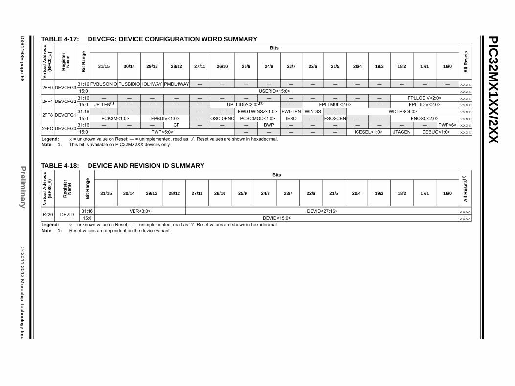
PIC
32MX
1XX
/2XX
DS
61168E-page 58
Prelim
ina
ry
2011-2012 Microchip T
echnology Inc.
All
Res
ets
20/4 19/3 18/2 17/1 16/0
— — — — — xxxx
xxxx
— — FPLLODIV<2:0> xxxx
0> — FPLLIDIV<2:0> xxxx
WDTPS<4:0> xxxx
— — FNOSC<2:0> xxxx
— — — — PWP<6> xxxx
ICESEL<1:0> JTAGEN DEBUG<1:0> xxxx
All
Re
set
s(1)
20/4 19/3 18/2 17/1 16/0
xxxx
xxxx
TABLE 4-17: DEVCFG: DEVICE CONFIGURATION WORD SUMMARYV
irtu
al A
dd
ress
(BF
C0_
#)
Re
gis
ter
Nam
e
Bit
Ra
ng
e
Bits
31/15 30/14 29/13 28/12 27/11 26/10 25/9 24/8 23/7 22/6 21/5
2FF0 DEVCFG331:16 FVBUSONIO FUSBIDIO IOL1WAY PMDL1WAY — — — — — — —
15:0 USERID<15:0>
2FF4 DEVCFG231:16 — — — — — — — — — — —
15:0 UPLLEN(1) — — — — UPLLIDIV<2:0>(1) — FPLLMUL<2:
2FF8 DEVCFG131:16 — — — — — — FWDTWINSZ<1:0> FWDTEN WINDIS —
15:0 FCKSM<1:0> FPBDIV<1:0> — OSCIOFNC POSCMOD<1:0> IESO — FSOSCEN
2FFC DEVCFG031:16 — — — CP — — — BWP — — —
15:0 PWP<5:0> — — — — —
Legend: x = unknown value on Reset; — = unimplemented, read as ‘0’. Reset values are shown in hexadecimal.Note 1: This bit is available on PIC32MX2XX devices only.
TABLE 4-18: DEVICE AND REVISION ID SUMMARY
Vir
tual
Ad
dre
ss(B
F8
0_#
)
Re
gis
ter
Na
me
Bit
Ran
ge
Bits
31/15 30/14 29/13 28/12 27/11 26/10 25/9 24/8 23/7 22/6 21/5
F220 DEVID31:16 VER<3:0> DEVID<27:16>
15:0 DEVID<15:0>
Legend: x = unknown value on Reset; — = unimplemented, read as ‘0’. Reset values are shown in hexadecimal.Note 1: Reset values are dependent on the device variant.
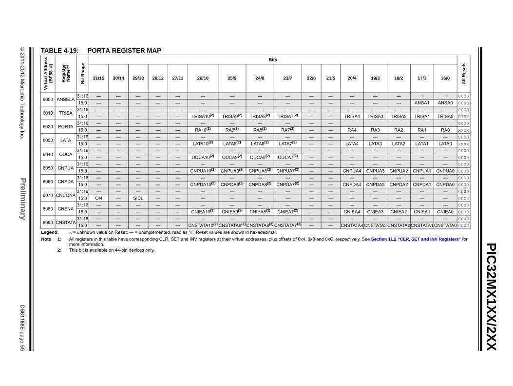
2011
-2012 Microchip T
echnology Inc.
Prelim
ina
ryD
S61168E
-page 59
PIC
32MX
1XX
/2XX
T
All
Res
ets
19/3 18/2 17/1 16/0
— — — — 0000
— — ANSA1 ANSA0 0003
— — — — 0000
4 TRISA3 TRISA2 TRISA1 TRISA0 079F
0000
RA3 RA2 RA1 RA0 xxxx
— — — — 0000
LATA3 LATA2 LATA1 LATA0 xxxx
— — — — 0000
— — — — 0000
— — — — 0000
4 CNPUA3 CNPUA2 CNPUA1 CNPUA0 0000
— — — — 0000
4 CNPDA3 CNPDA2 CNPDA1 CNPDA0 0000
— — — — 0000
— — — — 0000
— — — — 0000
4 CNIEA3 CNIEA2 CNIEA1 CNIEA0 0000
— — — — 0000
A4 CNSTATA3 CNSTATA2 CNSTATA1 CNSTATA0 0000
L
N ly. See Section 11.2 “CLR, SET and INV Registers” for
ABLE 4-19: PORTA REGISTER MAPV
irtu
al A
dd
ress
(BF
88
_#)
Re
gis
ter
Nam
e(1
)
Bit
Ra
ng
e
Bits
31/15 30/14 29/13 28/12 27/11 26/10 25/9 24/8 23/7 22/6 21/5 20/4
6000 ANSELA31:16 — — — — — — — — — — — —
15:0 — — — — — — — — — — — —
6010 TRISA31:16 — — — — — — — — — — — —
15:0 — — — — — TRISA10(2) TRISA9(2) TRISA8(2) TRISA7(2) — — TRISA
6020 PORTA31:16 — — — — — — — — — — —
15:0 — — — — — RA10(2) RA9(2) RA8(2) RA7(2) — — RA4
6030 LATA31:16 — — — — — — — — — — — —
15:0 — — — — — LATA10(2) LATA9(2) LATA8(2) LATA7(2) — — LATA4
6040 ODCA31:16 — — — — — — — — — — — —
15:0 — — — — — ODCA10(2) ODCA9(2) ODCA8(2) ODCA7(2) — — —
6050 CNPUA31:16 — — — — — — — — — — — —
15:0 — — — — — CNPUA10(2) CNPUA9(2) CNPUA8(2) CNPUA7(2) — — CNPUA
6060 CNPDA31:16 — — — — — — — — — — — —
15:0 — — — — — CNPDA10(2) CNPDA9(2) CNPDA8(2) CNPDA7(2) — — CNPDA
6070 CNCONA31:16 — — — — — — — — — — — —
15:0 ON — SIDL — — — — — — — — —
6080 CNENA31:16 — — — — — — — — — — — —
15:0 — — — — — CNIEA10(2) CNIEA9(2) CNIEA8(2) CNIEA7(2) — — CNIEA
6090 CNSTATA31:16 — — — — — — — — — — — —
15:0 — — — — — CNSTATA10(2) CNSTATA9(2) CNSTATA8(2) CNSTATA7(2) — — CNSTAT
egend: x = unknown value on Reset; — = unimplemented, read as ‘0’. Reset values are shown in hexadecimal.
ote 1: All registers in this table have corresponding CLR, SET and INV registers at their virtual addresses, plus offsets of 0x4, 0x8 and 0xC, respectivemore information.
2: This bit is available on 44-pin devices only.
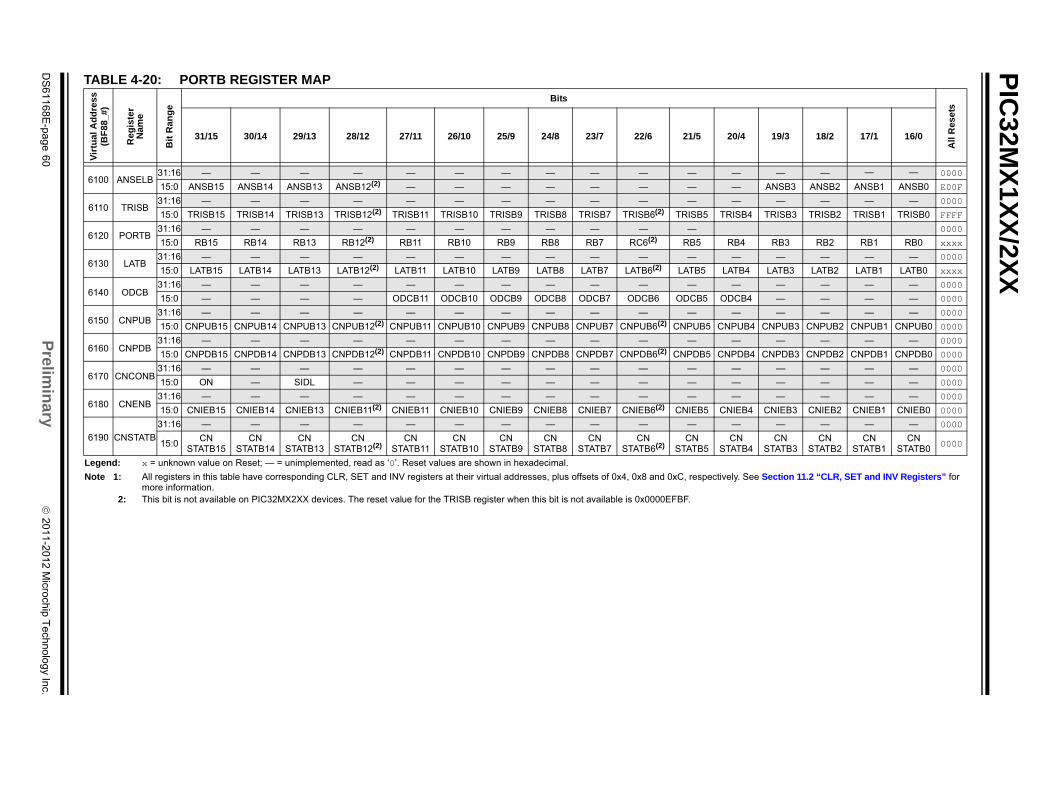
PIC
32MX
1XX
/2XX
DS
61168E-page 60
Prelim
ina
ry
2011-2012 Microchip T
echnology Inc.
All
Res
ets
20/4 19/3 18/2 17/1 16/0
— — — — — 0000
— ANSB3 ANSB2 ANSB1 ANSB0 E00F
— — — — — 0000
TRISB4 TRISB3 TRISB2 TRISB1 TRISB0 FFFF
0000
RB4 RB3 RB2 RB1 RB0 xxxx
— — — — — 0000
LATB4 LATB3 LATB2 LATB1 LATB0 xxxx
— — — — — 0000
ODCB4 — — — — 0000
— — — — — 0000
CNPUB4 CNPUB3 CNPUB2 CNPUB1 CNPUB0 0000
— — — — — 0000
CNPDB4 CNPDB3 CNPDB2 CNPDB1 CNPDB0 0000
— — — — — 0000
— — — — — 0000
— — — — — 0000
CNIEB4 CNIEB3 CNIEB2 CNIEB1 CNIEB0 0000
— — — — — 0000
CNSTATB4
CNSTATB3
CNSTATB2
CNSTATB1
CNSTATB0
0000
ctively. See Section 11.2 “CLR, SET and INV Registers” for
TABLE 4-20: PORTB REGISTER MAPV
irtu
al A
dd
ress
(BF
88
_#)
Re
gis
ter
Nam
e
Bit
Ra
ng
e
Bits
31/15 30/14 29/13 28/12 27/11 26/10 25/9 24/8 23/7 22/6 21/5
6100 ANSELB31:16 — — — — — — — — — — —
15:0 ANSB15 ANSB14 ANSB13 ANSB12(2) — — — — — — —
6110 TRISB31:16 — — — — — — — — — — —
15:0 TRISB15 TRISB14 TRISB13 TRISB12(2) TRISB11 TRISB10 TRISB9 TRISB8 TRISB7 TRISB6(2) TRISB5
6120 PORTB31:16 — — — — — — — — — — —
15:0 RB15 RB14 RB13 RB12(2) RB11 RB10 RB9 RB8 RB7 RC6(2) RB5
6130 LATB31:16 — — — — — — — — — — —
15:0 LATB15 LATB14 LATB13 LATB12(2) LATB11 LATB10 LATB9 LATB8 LATB7 LATB6(2) LATB5
6140 ODCB31:16 — — — — — — — — — — —
15:0 — — — — ODCB11 ODCB10 ODCB9 ODCB8 ODCB7 ODCB6 ODCB5
6150 CNPUB31:16 — — — — — — — — — — —
15:0 CNPUB15 CNPUB14 CNPUB13 CNPUB12(2) CNPUB11 CNPUB10 CNPUB9 CNPUB8 CNPUB7 CNPUB6(2) CNPUB5
6160 CNPDB31:16 — — — — — — — — — — —
15:0 CNPDB15 CNPDB14 CNPDB13 CNPDB12(2) CNPDB11 CNPDB10 CNPDB9 CNPDB8 CNPDB7 CNPDB6(2) CNPDB5
6170 CNCONB31:16 — — — — — — — — — — —
15:0 ON — SIDL — — — — — — — —
6180 CNENB31:16 — — — — — — — — — — —
15:0 CNIEB15 CNIEB14 CNIEB13 CNIEB11(2) CNIEB11 CNIEB10 CNIEB9 CNIEB8 CNIEB7 CNIEB6(2) CNIEB5
6190 CNSTATB
31:16 — — — — — — — — — — —
15:0CN
STATB15CN
STATB14CN
STATB13CN
STATB12(2)CN
STATB11CN
STATB10CN
STATB9CN
STATB8CN
STATB7CN
STATB6(2)CN
STATB5
Legend: x = unknown value on Reset; — = unimplemented, read as ‘0’. Reset values are shown in hexadecimal.
Note 1: All registers in this table have corresponding CLR, SET and INV registers at their virtual addresses, plus offsets of 0x4, 0x8 and 0xC, respemore information.
2: This bit is not available on PIC32MX2XX devices. The reset value for the TRISB register when this bit is not available is 0x0000EFBF.
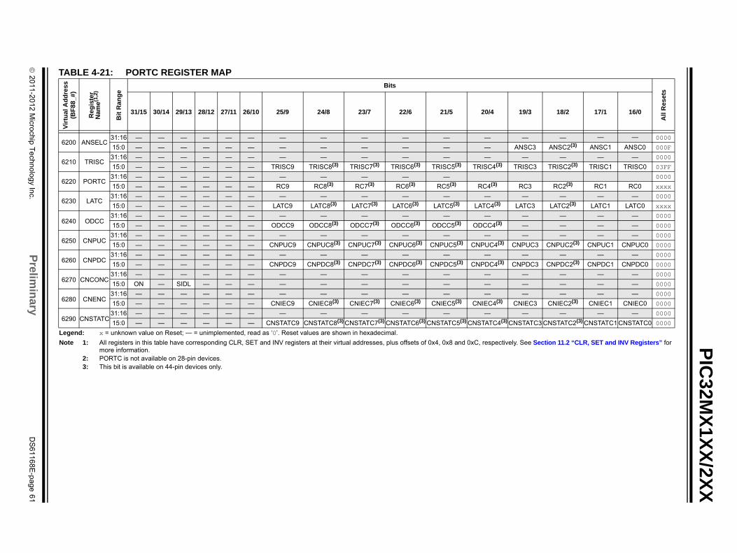
2011
-2012 Microchip T
echnology Inc.
Prelim
ina
ryD
S61168E
-page 61
PIC
32MX
1XX
/2XX
T
All
Res
ets
19/3 18/2 17/1 16/0
— — — — 0000
ANSC3 ANSC2(3) ANSC1 ANSC0 000F
— — — — 0000
TRISC3 TRISC2(3) TRISC1 TRISC0 03FF
0000
RC3 RC2(3) RC1 RC0 xxxx
— — — — 0000
LATC3 LATC2(3) LATC1 LATC0 xxxx
— — — — 0000
— — — — 0000
— — — — 0000
NPUC3 CNPUC2(3) CNPUC1 CNPUC0 0000
— — — — 0000
NPDC3 CNPDC2(3) CNPDC1 CNPDC0 0000
— — — — 0000
— — — — 0000
— — — — 0000
CNIEC3 CNIEC2(3) CNIEC1 CNIEC0 0000
— — — — 0000
NSTATC3 CNSTATC2(3) CNSTATC1 CNSTATC0 0000
L
N ly. See Section 11.2 “CLR, SET and INV Registers” for
ABLE 4-21: PORTC REGISTER MAPV
irtu
al A
dd
ress
(BF
88
_#)
Re
gis
ter
Nam
e(1
,2)
Bit
Ra
ng
e
Bits
31/15 30/14 29/13 28/12 27/11 26/10 25/9 24/8 23/7 22/6 21/5 20/4
6200 ANSELC31:16 — — — — — — — — — — — —
15:0 — — — — — — — — — — — —
6210 TRISC31:16 — — — — — — — — — — — —
15:0 — — — — — — TRISC9 TRISC8(3) TRISC7(3) TRISC6(3) TRISC5(3) TRISC4(3)
6220 PORTC31:16 — — — — — — — — — — —
15:0 — — — — — — RC9 RC8(3) RC7(3) RC6(3) RC5(3) RC4(3)
6230 LATC31:16 — — — — — — — — — — — —
15:0 — — — — — — LATC9 LATC8(3) LATC7(3) LATC6(3) LATC5(3) LATC4(3)
6240 ODCC31:16 — — — — — — — — — — — —
15:0 — — — — — — ODCC9 ODCC8(3) ODCC7(3) ODCC6(3) ODCC5(3) ODCC4(3)
6250 CNPUC31:16 — — — — — — — — — — — —
15:0 — — — — — — CNPUC9 CNPUC8(3) CNPUC7(3) CNPUC6(3) CNPUC5(3) CNPUC4(3) C
6260 CNPDC31:16 — — — — — — — — — — — —
15:0 — — — — — — CNPDC9 CNPDC8(3) CNPDC7(3) CNPDC6(3) CNPDC5(3) CNPDC4(3) C
6270 CNCONC31:16 — — — — — — — — — — — —
15:0 ON — SIDL — — — — — — — — —
6280 CNENC31:16 — — — — — — — — — — — —
15:0 — — — — — — CNIEC9 CNIEC8(3) CNIEC7(3) CNIEC6(3) CNIEC5(3) CNIEC4(3)
6290 CNSTATC31:16 — — — — — — — — — — — —
15:0 — — — — — — CNSTATC9 CNSTATC8(3) CNSTATC7(3) CNSTATC6(3) CNSTATC5(3) CNSTATC4(3) C
egend: x = unknown value on Reset; — = unimplemented, read as ‘0’. Reset values are shown in hexadecimal.
ote 1: All registers in this table have corresponding CLR, SET and INV registers at their virtual addresses, plus offsets of 0x4, 0x8 and 0xC, respectivemore information.
2: PORTC is not available on 28-pin devices.3: This bit is available on 44-pin devices only.
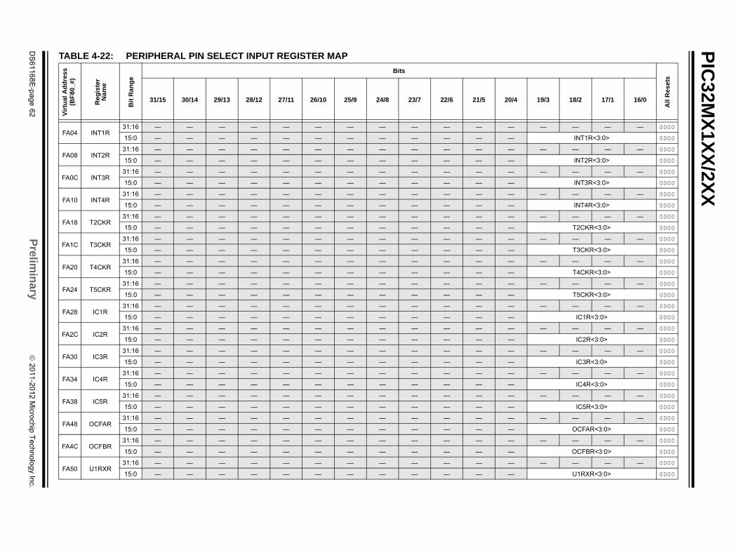
PIC
32MX
1XX
/2XX
DS
61168E-page 62
Prelim
ina
ry
2011-2012 Microchip T
echnology Inc.
All
Re
set
s
20/4 19/3 18/2 17/1 16/0
— — — — — 0000
— INT1R<3:0> 0000
— — — — — 0000
— INT2R<3:0> 0000
— — — — — 0000
— INT3R<3:0> 0000
— — — — — 0000
— INT4R<3:0> 0000
— — — — — 0000
— T2CKR<3:0> 0000
— — — — — 0000
— T3CKR<3:0> 0000
— — — — — 0000
— T4CKR<3:0> 0000
— — — — — 0000
— T5CKR<3:0> 0000
— — — — — 0000
— IC1R<3:0> 0000
— — — — — 0000
— IC2R<3:0> 0000
— — — — — 0000
— IC3R<3:0> 0000
— — — — — 0000
— IC4R<3:0> 0000
— — — — — 0000
— IC5R<3:0> 0000
— — — — — 0000
— OCFAR<3:0> 0000
— — — — — 0000
— OCFBR<3:0> 0000
— — — — — 0000
— U1RXR<3:0> 0000
TABLE 4-22: PERIPHERAL PIN SELECT INPUT REGISTER MAPV
irtu
al A
dd
ress
(BF
80_
#)
Re
gis
ter
Na
me
Bit
Ran
ge
Bits
31/15 30/14 29/13 28/12 27/11 26/10 25/9 24/8 23/7 22/6 21/5
FA04 INT1R31:16 — — — — — — — — — — —
15:0 — — — — — — — — — — —
FA08 INT2R31:16 — — — — — — — — — — —
15:0 — — — — — — — — — — —
FA0C INT3R31:16 — — — — — — — — — — —
15:0 — — — — — — — — — — —
FA10 INT4R31:16 — — — — — — — — — — —
15:0 — — — — — — — — — — —
FA18 T2CKR31:16 — — — — — — — — — — —
15:0 — — — — — — — — — — —
FA1C T3CKR31:16 — — — — — — — — — — —
15:0 — — — — — — — — — — —
FA20 T4CKR31:16 — — — — — — — — — — —
15:0 — — — — — — — — — — —
FA24 T5CKR31:16 — — — — — — — — — — —
15:0 — — — — — — — — — — —
FA28 IC1R31:16 — — — — — — — — — — —
15:0 — — — — — — — — — — —
FA2C IC2R31:16 — — — — — — — — — — —
15:0 — — — — — — — — — — —
FA30 IC3R31:16 — — — — — — — — — — —
15:0 — — — — — — — — — — —
FA34 IC4R31:16 — — — — — — — — — — —
15:0 — — — — — — — — — — —
FA38 IC5R31:16 — — — — — — — — — — —
15:0 — — — — — — — — — — —
FA48 OCFAR31:16 — — — — — — — — — — —
15:0 — — — — — — — — — — —
FA4C OCFBR31:16 — — — — — — — — — — —
15:0 — — — — — — — — — — —
FA50 U1RXR31:16 — — — — — — — — — — —
15:0 — — — — — — — — — — —
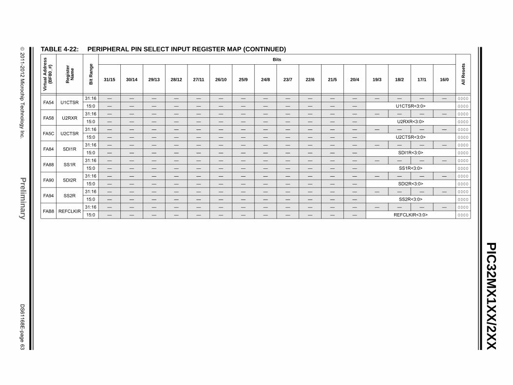
2011
-2012 Microchip T
echnology Inc.
Prelim
ina
ryD
S61168E
-page 63
PIC
32MX
1XX
/2XX
— — — — 0000
U1CTSR<3:0> 0000
— — — — 0000
U2RXR<3:0> 0000
— — — — 0000
U2CTSR<3:0> 0000
— — — — 0000
SDI1R<3:0> 0000
— — — — 0000
SS1R<3:0> 0000
— — — — 0000
SDI2R<3:0> 0000
— — — — 0000
SS2R<3:0> 0000
— — — — 0000
REFCLKIR<3:0> 0000
T
All
Res
ets
4 19/3 18/2 17/1 16/0
FA54 U1CTSR31:16 — — — — — — — — — — — —
15:0 — — — — — — — — — — — —
FA58 U2RXR31:16 — — — — — — — — — — — —
15:0 — — — — — — — — — — — —
FA5C U2CTSR31:16 — — — — — — — — — — — —
15:0 — — — — — — — — — — — —
FA84 SDI1R31:16 — — — — — — — — — — — —
15:0 — — — — — — — — — — — —
FA88 SS1R31:16 — — — — — — — — — — — —
15:0 — — — — — — — — — — — —
FA90 SDI2R31:16 — — — — — — — — — — — —
15:0 — — — — — — — — — — — —
FA94 SS2R31:16 — — — — — — — — — — — —
15:0 — — — — — — — — — — — —
FAB8 REFCLKIR31:16 — — — — — — — — — — — —
15:0 — — — — — — — — — — — —
ABLE 4-22: PERIPHERAL PIN SELECT INPUT REGISTER MAP (CONTINUED)V
irtu
al A
dd
ress
(BF
80
_#)
Re
gis
ter
Nam
e
Bit
Ra
ng
e
Bits
31/15 30/14 29/13 28/12 27/11 26/10 25/9 24/8 23/7 22/6 21/5 20/
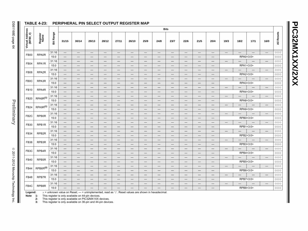
PIC
32MX
1XX
/2XX
DS
61168E-page 64
Prelim
ina
ry
2011-2012 Microchip T
echnology Inc.
All
Re
set
s
20/4 19/3 18/2 17/1 16/0
— — — — — 0000
— RPA0<3:0> 0000
— — — — — 0000
— RPA1<3:0> 0000
— — — — — 0000
— RPA2<3:0> 0000
— — — — — 0000
— RPA3<3:0> 0000
— — — — — 0000
— RPA4<3:0> 0000
— — — — — 0000
— RPA8<3:0> 0000
— — — — — 0000
— RPA9<3:0> 0000
— — — — — 0000
— RPB0<3:0> 0000
— — — — — 0000
— RPB1<3:0> 0000
— — — — — 0000
— RPB2<3:0> 0000
— — — — — 0000
— RPB3<3:0> 0000
— — — — — 0000
— RPB4<3:0> 0000
— — — — — 0000
— RPB5<3:0> 0000
— — — — — 0000
— RPB6<3:0> 0000
— — — — — 0000
— RPB7<3:0> 0000
— — — — — 0000
— RPB8<3:0> 0000
TABLE 4-23: PERIPHERAL PIN SELECT OUTPUT REGISTER MAPV
irtu
al A
dd
ress
(BF
80_
#)
Re
gis
ter
Na
me
Bit
Ran
ge
Bits
31/15 30/14 29/13 28/12 27/11 26/10 25/9 24/8 23/7 22/6 21/5
FB00 RPA0R31:16 — — — — — — — — — — —
15:0 — — — — — — — — — — —
FB04 RPA1R31:16 — — — — — — — — — — —
15:0 — — — — — — — — — — —
FB08 RPA2R31:16 — — — — — — — — — — —
15:0 — — — — — — — — — — —
FB0C RPA3R31:16 — — — — — — — — — — —
15:0 — — — — — — — — — — —
FB10 RPA4R31:16 — — — — — — — — — — —
15:0 — — — — — — — — — — —
FB20 RPA8R(1)31:16 — — — — — — — — — — —
15:0 — — — — — — — — — — —
FB24 RPA9R(1)31:16 — — — — — — — — — — —
15:0 — — — — — — — — — — —
FB2C RPB0R31:16 — — — — — — — — — — —
15:0 — — — — — — — — — — —
FB30 RPB1R31:16 — — — — — — — — — — —
15:0 — — — — — — — — — — —
FB34 RPB2R31:16 — — — — — — — — — — —
15:0 — — — — — — — — — — —
FB38 RPB3R31:16 — — — — — — — — — — —
15:0 — — — — — — — — — — —
FB3C RPB4R31:16 — — — — — — — — — — —
15:0 — — — — — — — — — — —
FB40 RPB5R31:16 — — — — — — — — — — —
15:0 — — — — — — — — — — —
FB44 RPB6R(2)31:16 — — — — — — — — — — —
15:0 — — — — — — — — — — —
FB48 RPB7R31:16 — — — — — — — — — — —
15:0 — — — — — — — — — — —
FB4C RPB8R31:16 — — — — — — — — — — —
15:0 — — — — — — — — — — —
Legend: x = unknown value on Reset; — = unimplemented, read as ‘0’. Reset values are shown in hexadecimal.Note 1: This register is only available on 44-pin devices.
2: This register is only available on PIC32MX1XX devices.3: This register is only available on 36-pin and 44-pin devices.
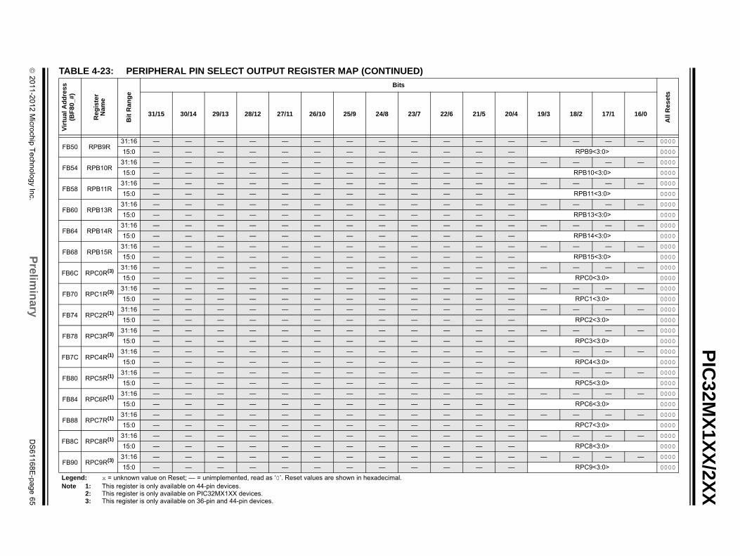
2011
-2012 Microchip T
echnology Inc.
Prelim
ina
ryD
S61168E
-page 65
PIC
32MX
1XX
/2XX
— — — — 0000
RPB9<3:0> 0000
— — — — 0000
RPB10<3:0> 0000
— — — — 0000
RPB11<3:0> 0000
— — — — 0000
RPB13<3:0> 0000
— — — — 0000
RPB14<3:0> 0000
— — — — 0000
RPB15<3:0> 0000
— — — — 0000
RPC0<3:0> 0000
— — — — 0000
RPC1<3:0> 0000
— — — — 0000
RPC2<3:0> 0000
— — — — 0000
RPC3<3:0> 0000
— — — — 0000
RPC4<3:0> 0000
— — — — 0000
RPC5<3:0> 0000
— — — — 0000
RPC6<3:0> 0000
— — — — 0000
RPC7<3:0> 0000
— — — — 0000
RPC8<3:0> 0000
— — — — 0000
RPC9<3:0> 0000
T
All
Res
ets
19/3 18/2 17/1 16/0
FB50 RPB9R31:16 — — — — — — — — — — — —
15:0 — — — — — — — — — — — —
FB54 RPB10R31:16 — — — — — — — — — — — —
15:0 — — — — — — — — — — — —
FB58 RPB11R31:16 — — — — — — — — — — — —
15:0 — — — — — — — — — — — —
FB60 RPB13R31:16 — — — — — — — — — — — —
15:0 — — — — — — — — — — — —
FB64 RPB14R31:16 — — — — — — — — — — — —
15:0 — — — — — — — — — — — —
FB68 RPB15R31:16 — — — — — — — — — — — —
15:0 — — — — — — — — — — — —
FB6C RPC0R(3)31:16 — — — — — — — — — — — —
15:0 — — — — — — — — — — — —
FB70 RPC1R(3)31:16 — — — — — — — — — — — —
15:0 — — — — — — — — — — — —
FB74 RPC2R(1)31:16 — — — — — — — — — — — —
15:0 — — — — — — — — — — — —
FB78 RPC3R(3)31:16 — — — — — — — — — — — —
15:0 — — — — — — — — — — — —
FB7C RPC4R(1)31:16 — — — — — — — — — — — —
15:0 — — — — — — — — — — — —
FB80 RPC5R(1)31:16 — — — — — — — — — — — —
15:0 — — — — — — — — — — — —
FB84 RPC6R(1)31:16 — — — — — — — — — — — —
15:0 — — — — — — — — — — — —
FB88 RPC7R(1)31:16 — — — — — — — — — — — —
15:0 — — — — — — — — — — — —
FB8C RPC8R(1)31:16 — — — — — — — — — — — —
15:0 — — — — — — — — — — — —
FB90 RPC9R(3)31:16 — — — — — — — — — — — —
15:0 — — — — — — — — — — — —
ABLE 4-23: PERIPHERAL PIN SELECT OUTPUT REGISTER MAP (CONTINUED)V
irtu
al A
dd
ress
(BF
80
_#)
Re
gis
ter
Nam
e
Bit
Ra
ng
e
Bits
31/15 30/14 29/13 28/12 27/11 26/10 25/9 24/8 23/7 22/6 21/5 20/4
Legend: x = unknown value on Reset; — = unimplemented, read as ‘0’. Reset values are shown in hexadecimal.Note 1: This register is only available on 44-pin devices.
2: This register is only available on PIC32MX1XX devices.3: This register is only available on 36-pin and 44-pin devices.
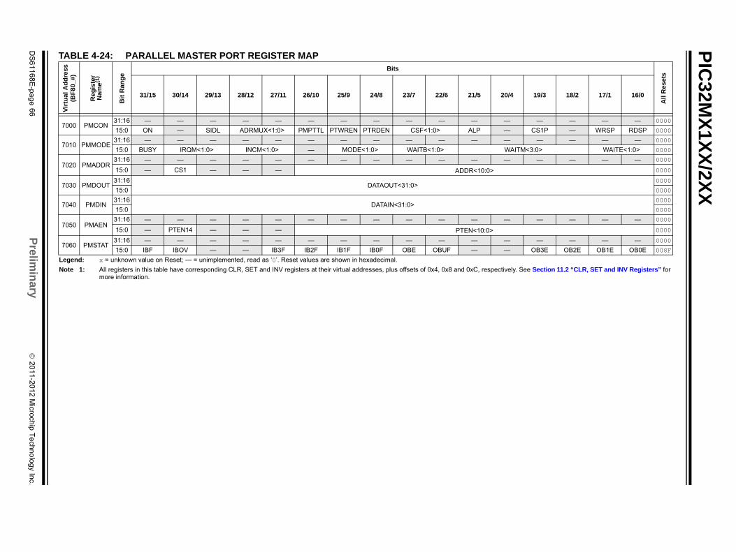
PIC
32MX
1XX
/2XX
DS
61168E-page 66
Prelim
ina
ry
2011-2012 Microchip T
echnology Inc.
All
Res
ets
20/4 19/3 18/2 17/1 16/0
— — — — — 0000
— CS1P — WRSP RDSP 0000
— — — — — 0000
WAITM<3:0> WAITE<1:0> 0000
— — — — — 0000
0000
0000
0000
0000
0000
— — — — — 0000
0000
— — — — — 0000
— OB3E OB2E OB1E OB0E 008F
ctively. See Section 11.2 “CLR, SET and INV Registers” for
TABLE 4-24: PARALLEL MASTER PORT REGISTER MAPV
irtu
al A
dd
ress
(BF
80
_#)
Re
gis
ter
Nam
e(1
)
Bit
Ra
ng
e
Bits
31/15 30/14 29/13 28/12 27/11 26/10 25/9 24/8 23/7 22/6 21/5
7000 PMCON31:16 — — — — — — — — — — —
15:0 ON — SIDL ADRMUX<1:0> PMPTTL PTWREN PTRDEN CSF<1:0> ALP
7010 PMMODE31:16 — — — — — — — — — — —
15:0 BUSY IRQM<1:0> INCM<1:0> — MODE<1:0> WAITB<1:0>
7020 PMADDR31:16 — — — — — — — — — — —
15:0 — CS1 — — — ADDR<10:0>
7030 PMDOUT31:16
DATAOUT<31:0>15:0
7040 PMDIN31:16
DATAIN<31:0>15:0
7050 PMAEN31:16 — — — — — — — — — — —
15:0 — PTEN14 — — — PTEN<10:0>
7060 PMSTAT31:16 — — — — — — — — — — —
15:0 IBF IBOV — — IB3F IB2F IB1F IB0F OBE OBUF —
Legend: x = unknown value on Reset; — = unimplemented, read as ‘0’. Reset values are shown in hexadecimal.
Note 1: All registers in this table have corresponding CLR, SET and INV registers at their virtual addresses, plus offsets of 0x4, 0x8 and 0xC, respemore information.
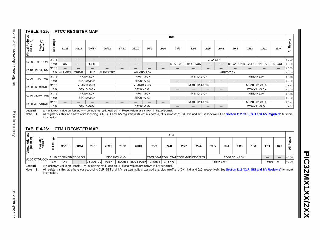
2011
-2012 Microchip T
echnology Inc.
Prelim
ina
ryD
S61168E
-page 67
PIC
32MX
1XX
/2XX
T
All
Res
ets
4 19/3 18/2 17/1 16/0
0000
RTCWREN RTCSYNC HALFSEC RTCOE 0000
— — — — 0000
PT<7:0> 0000
MIN01<3:0> xxxx
— — — — xx00
MONTH01<3:0> xxxx
WDAY01<3:0> xx00
MIN01<3:0> xxxx
— — — — xx00
MONTH01<3:0> 00xx
WDAY01<3:0> xx0x
LN e Section 11.2 “CLR, SET and INV Registers” for more
T
All
Re
se
ts
20/4 19/3 18/2 17/1 16/0
EDG2SEL<3:0> — — 0000
:0> IRNG<1:0> 0000
LN e Section 11.2 “CLR, SET and INV Registers” for more
ABLE 4-25: RTCC REGISTER MAPV
irtu
al A
dd
ress
(BF
80
_#)
Re
gis
ter
Nam
e(1
)
Bit
Ra
ng
e
Bits
31/15 30/14 29/13 28/12 27/11 26/10 25/9 24/8 23/7 22/6 21/5 20/
0200 RTCCON31:16 — — — — — — CAL<9:0>
15:0 ON — SIDL — — — — — RTSECSEL RTCCLKON — —
0210 RTCALRM31:16 — — — — — — — — — — — —
15:0 ALRMEN CHIME PIV ALRMSYNC AMASK<3:0> AR
0220 RTCTIME31:16 HR10<3:0> HR01<3:0> MIN10<3:0>
15:0 SEC10<3:0> SEC01<3:0> — — — —
0230 RTCDATE31:16 YEAR10<3:0> YEAR01<3:0> MONTH10<3:0>
15:0 DAY10<3:0> DAY01<3:0> — — — —
0240 ALRMTIME31:16 HR10<3:0> HR01<3:0> MIN10<3:0>
15:0 SEC10<3:0> SEC01<3:0> — — — —
0250 ALRMDATE31:16 — — — — — — — — MONTH10<3:0>
15:0 DAY10<3:0> DAY01<3:0> — — — —
egend: x = unknown value on Reset; — = unimplemented, read as ‘0’. Reset values are shown in hexadecimal.ote 1: All registers in this table have corresponding CLR, SET and INV registers at its virtual address, plus an offset of 0x4, 0x8 and 0xC, respectively. Se
information.
ABLE 4-26: CTMU REGISTER MAP
Vir
tual
Ad
dre
ss(B
F8
0_#
)
Re
gis
ter
Nam
e(1
)
Bit
Ra
ng
e
Bits
31/15 30/14 29/13 28/12 27/11 26/10 25/9 24/8 23/7 22/6 21/5
A200 CTMUCON31:16 EDG1MOD EDG1POL EDG1SEL<3:0> EDG2STAT EDG1STAT EDG2MOD EDG2POL
15:0 ON — CTMUSIDL TGEN EDGEN EDGSEQEN IDISSEN CTTRIG ITRIM<5
egend: x = unknown value on Reset; — = unimplemented, read as ‘0’. Reset values are shown in hexadecimal.ote 1: All registers in this table have corresponding CLR, SET and INV registers at its virtual address, plus an offset of 0x4, 0x8 and 0xC, respectively. Se
information.
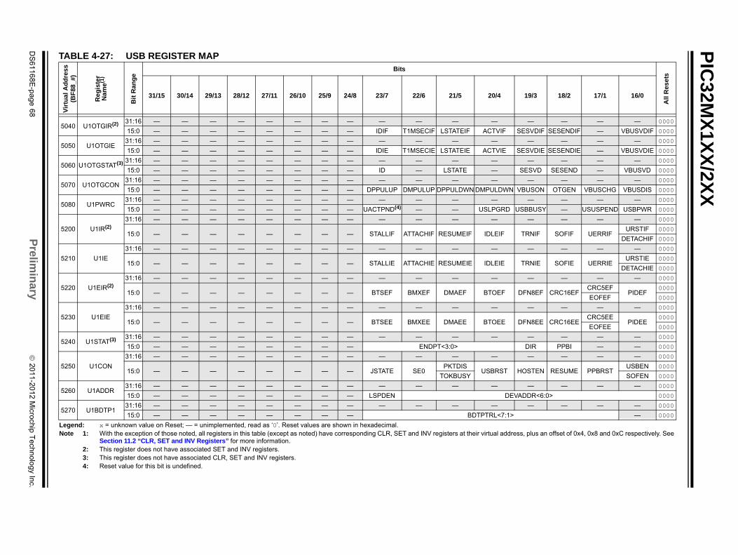
PIC
32MX
1XX
/2XX
DS
61168E-page 68
Prelim
ina
ry
2011-2012 Microchip T
echnology Inc.
All
Res
ets
4 19/3 18/2 17/1 16/0
— — — — 0000
IF SESVDIF SESENDIF — VBUSVDIF 0000
— — — — 0000
IE SESVDIE SESENDIE — VBUSVDIE 0000
— — — — 0000
SESVD SESEND — VBUSVD 0000
— — — — 0000
DWN VBUSON OTGEN VBUSCHG VBUSDIS 0000
— — — — 0000
RD USBBUSY — USUSPEND USBPWR 0000
— — — — 0000
IF TRNIF SOFIF UERRIFURSTIF 0000
DETACHIF 0000
— — — — 0000
IE TRNIE SOFIE UERRIEURSTIE 0000
DETACHIE 0000
— — — — 0000
EF DFN8EF CRC16EFCRC5EF
PIDEF0000
EOFEF 0000
— — — — 0000
EE DFN8EE CRC16EECRC5EE
PIDEE0000
EOFEE 0000
— — — — 0000
DIR PPBI — — 0000
— — — — 0000
ST HOSTEN RESUME PPBRSTUSBEN 0000
SOFEN 0000
— — — — 0000
DEVADDR<6:0> 0000
— — — — 0000
<7:1> — 0000
l address, plus an offset of 0x4, 0x8 and 0xC respectively. See
TABLE 4-27: USB REGISTER MAPV
irtu
al A
dd
ress
(BF
88
_#)
Re
gis
ter
Nam
e(1
)
Bit
Ra
ng
e
Bits
31/15 30/14 29/13 28/12 27/11 26/10 25/9 24/8 23/7 22/6 21/5 20/
5040 U1OTGIR(2) 31:16 — — — — — — — — — — — —
15:0 — — — — — — — — IDIF T1MSECIF LSTATEIF ACTV
5050 U1OTGIE31:16 — — — — — — — — — — — —
15:0 — — — — — — — — IDIE T1MSECIE LSTATEIE ACTV
5060 U1OTGSTAT(3) 31:16 — — — — — — — — — — — —
15:0 — — — — — — — — ID — LSTATE —
5070 U1OTGCON31:16 — — — — — — — — — — — —
15:0 — — — — — — — — DPPULUP DMPULUP DPPULDWN DMPUL
5080 U1PWRC31:16 — — — — — — — — — — — —
15:0 — — — — — — — — UACTPND(4) — — USLPG
5200 U1IR(2)31:16 — — — — — — — — — — — —
15:0 — — — — — — — — STALLIF ATTACHIF RESUMEIF IDLE
5210 U1IE
31:16 — — — — — — — — — — — —
15:0 — — — — — — — — STALLIE ATTACHIE RESUMEIE IDLE
5220 U1EIR(2)31:16 — — — — — — — — — — — —
15:0 — — — — — — — — BTSEF BMXEF DMAEF BTO
5230 U1EIE
31:16 — — — — — — — — — — — —
15:0 — — — — — — — — BTSEE BMXEE DMAEE BTO
5240 U1STAT(3) 31:16 — — — — — — — — — — — —
15:0 — — — — — — — — ENDPT<3:0>
5250 U1CON
31:16 — — — — — — — — — — — —
15:0 — — — — — — — — JSTATE SE0PKTDIS
USBRTOKBUSY
5260 U1ADDR31:16 — — — — — — — — — — — —
15:0 — — — — — — — — LSPDEN
5270 U1BDTP131:16 — — — — — — — — — — — —
15:0 — — — — — — — — BDTPTRL
Legend: x = unknown value on Reset; — = unimplemented, read as ‘0’. Reset values are shown in hexadecimal.Note 1: With the exception of those noted, all registers in this table (except as noted) have corresponding CLR, SET and INV registers at their virtua
Section 11.2 “CLR, SET and INV Registers” for more information.2: This register does not have associated SET and INV registers.3: This register does not have associated CLR, SET and INV registers.4: Reset value for this bit is undefined.
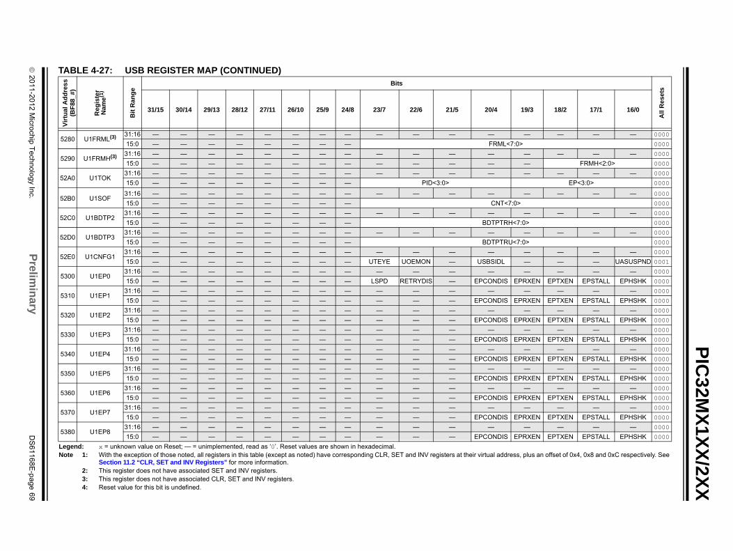
2011
-2012 Microchip T
echnology Inc.
Prelim
ina
ryD
S61168E
-page 69
PIC
32MX
1XX
/2XX
— — — — 0000
7:0> 0000
— — — — 0000
— FRMH<2:0> 0000
— — — — 0000
EP<3:0> 0000
— — — — 0000
:0> 0000
— — — — 0000
<7:0> 0000
— — — — 0000
<7:0> 0000
— — — — 0000
— — — UASUSPND 0001
— — — — 0000
EPRXEN EPTXEN EPSTALL EPHSHK 0000
— — — — 0000
EPRXEN EPTXEN EPSTALL EPHSHK 0000
— — — — 0000
EPRXEN EPTXEN EPSTALL EPHSHK 0000
— — — — 0000
EPRXEN EPTXEN EPSTALL EPHSHK 0000
— — — — 0000
EPRXEN EPTXEN EPSTALL EPHSHK 0000
— — — — 0000
EPRXEN EPTXEN EPSTALL EPHSHK 0000
— — — — 0000
EPRXEN EPTXEN EPSTALL EPHSHK 0000
— — — — 0000
EPRXEN EPTXEN EPSTALL EPHSHK 0000
— — — — 0000
EPRXEN EPTXEN EPSTALL EPHSHK 0000
T
All
Re
sets
19/3 18/2 17/1 16/0
LN ess, plus an offset of 0x4, 0x8 and 0xC respectively. See
5280 U1FRML(3) 31:16 — — — — — — — — — — — —
15:0 — — — — — — — — FRML<
5290 U1FRMH(3) 31:16 — — — — — — — — — — — —
15:0 — — — — — — — — — — — —
52A0 U1TOK31:16 — — — — — — — — — — — —
15:0 — — — — — — — — PID<3:0>
52B0 U1SOF31:16 — — — — — — — — — — — —
15:0 — — — — — — — — CNT<7
52C0 U1BDTP231:16 — — — — — — — — — — — —
15:0 — — — — — — — — BDTPTRH
52D0 U1BDTP331:16 — — — — — — — — — — — —
15:0 — — — — — — — — BDTPTRU
52E0 U1CNFG131:16 — — — — — — — — — — — —
15:0 — — — — — — — — UTEYE UOEMON — USBSIDL
5300 U1EP031:16 — — — — — — — — — — — —
15:0 — — — — — — — — LSPD RETRYDIS — EPCONDIS
5310 U1EP131:16 — — — — — — — — — — — —
15:0 — — — — — — — — — — — EPCONDIS
5320 U1EP231:16 — — — — — — — — — — — —
15:0 — — — — — — — — — — — EPCONDIS
5330 U1EP331:16 — — — — — — — — — — — —
15:0 — — — — — — — — — — — EPCONDIS
5340 U1EP431:16 — — — — — — — — — — — —
15:0 — — — — — — — — — — — EPCONDIS
5350 U1EP531:16 — — — — — — — — — — — —
15:0 — — — — — — — — — — — EPCONDIS
5360 U1EP631:16 — — — — — — — — — — — —
15:0 — — — — — — — — — — — EPCONDIS
5370 U1EP731:16 — — — — — — — — — — — —
15:0 — — — — — — — — — — — EPCONDIS
5380 U1EP831:16 — — — — — — — — — — — —
15:0 — — — — — — — — — — — EPCONDIS
ABLE 4-27: USB REGISTER MAP (CONTINUED)V
irtu
al A
dd
res
s(B
F88
_#
)
Reg
iste
rN
ame
(1)
Bit
Ran
ge
Bits
31/15 30/14 29/13 28/12 27/11 26/10 25/9 24/8 23/7 22/6 21/5 20/4
egend: x = unknown value on Reset; — = unimplemented, read as ‘0’. Reset values are shown in hexadecimal.ote 1: With the exception of those noted, all registers in this table (except as noted) have corresponding CLR, SET and INV registers at their virtual addr
Section 11.2 “CLR, SET and INV Registers” for more information.2: This register does not have associated SET and INV registers.3: This register does not have associated CLR, SET and INV registers.4: Reset value for this bit is undefined.
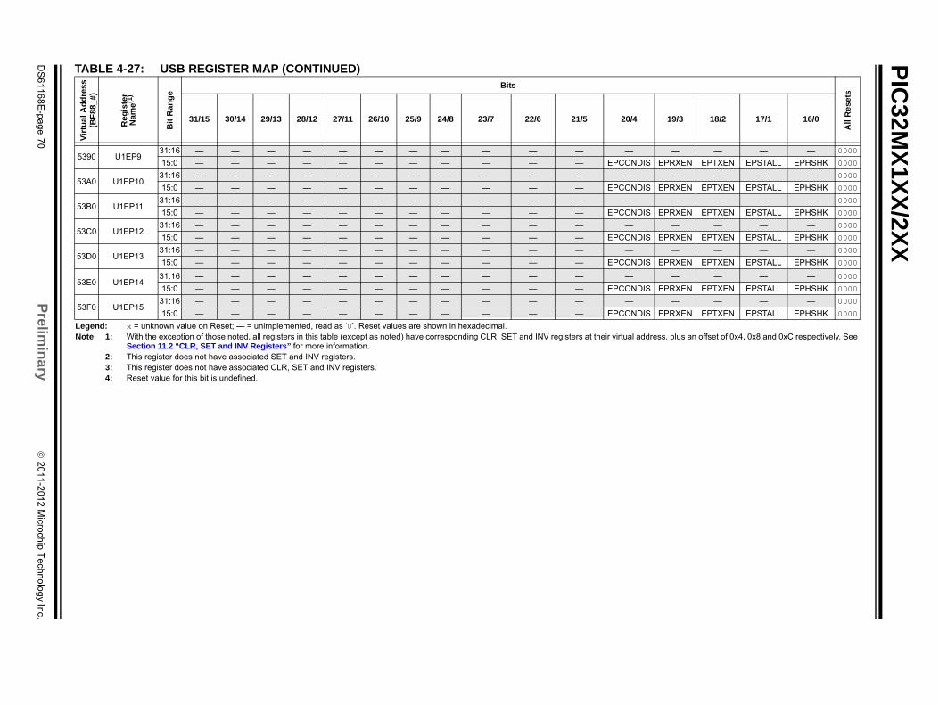
PIC
32MX
1XX
/2XX
DS
61168E-page 70
Prelim
ina
ry
2011-2012 Microchip T
echnology Inc.
— — — — 0000
NDIS EPRXEN EPTXEN EPSTALL EPHSHK 0000
— — — — 0000
NDIS EPRXEN EPTXEN EPSTALL EPHSHK 0000
— — — — 0000
NDIS EPRXEN EPTXEN EPSTALL EPHSHK 0000
— — — — 0000
NDIS EPRXEN EPTXEN EPSTALL EPHSHK 0000
— — — — 0000
NDIS EPRXEN EPTXEN EPSTALL EPHSHK 0000
— — — — 0000
NDIS EPRXEN EPTXEN EPSTALL EPHSHK 0000
— — — — 0000
NDIS EPRXEN EPTXEN EPSTALL EPHSHK 0000
All
Re
sets
4 19/3 18/2 17/1 16/0
l address, plus an offset of 0x4, 0x8 and 0xC respectively. See
5390 U1EP931:16 — — — — — — — — — — — —
15:0 — — — — — — — — — — — EPCO
53A0 U1EP1031:16 — — — — — — — — — — — —
15:0 — — — — — — — — — — — EPCO
53B0 U1EP1131:16 — — — — — — — — — — — —
15:0 — — — — — — — — — — — EPCO
53C0 U1EP1231:16 — — — — — — — — — — — —
15:0 — — — — — — — — — — — EPCO
53D0 U1EP1331:16 — — — — — — — — — — — —
15:0 — — — — — — — — — — — EPCO
53E0 U1EP1431:16 — — — — — — — — — — — —
15:0 — — — — — — — — — — — EPCO
53F0 U1EP1531:16 — — — — — — — — — — — —
15:0 — — — — — — — — — — — EPCO
TABLE 4-27: USB REGISTER MAP (CONTINUED)V
irtu
al A
dd
res
s(B
F88
_#
)
Reg
iste
rN
ame
(1)
Bit
Ran
ge
Bits
31/15 30/14 29/13 28/12 27/11 26/10 25/9 24/8 23/7 22/6 21/5 20/
Legend: x = unknown value on Reset; — = unimplemented, read as ‘0’. Reset values are shown in hexadecimal.Note 1: With the exception of those noted, all registers in this table (except as noted) have corresponding CLR, SET and INV registers at their virtua
Section 11.2 “CLR, SET and INV Registers” for more information.2: This register does not have associated SET and INV registers.3: This register does not have associated CLR, SET and INV registers.4: Reset value for this bit is undefined.
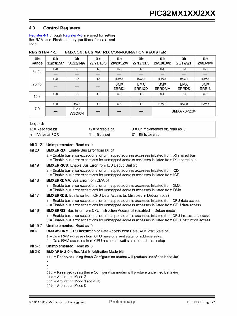
PIC32MX1XX/2XX
4.3 Control Registers
Register 4-1 through Register 4-8 are used for settingthe RAM and Flash memory partitions for data andcode.
REGISTER 4-1: BMXCON: BUS MATRIX CONFIGURATION REGISTER
Bit Range
Bit31/23/15/7
Bit30/22/14/6
Bit29/21/13/5
Bit28/20/12/4
Bit27/19/11/3
Bit26/18/10/2
Bit25/17/9/1
Bit24/16/8/0
31:24U-0 U-0 U-0 U-0 U-0 U-0 U-0 U-0
— — — — — — — —
23:16
U-0 U-0 U-0 R/W-1 R/W-1 R/W-1 R/W-1 R/W-1
— — —BMX
ERRIXIBMX
ERRICDBMX
ERRDMABMX
ERRDSBMX
ERRIS
15:8U-0 U-0 U-0 U-0 U-0 U-0 U-0 U-0
— — — — — — — —
7:0
U-0 R/W-1 U-0 U-0 U-0 R/W-0 R/W-0 R/W-1
—BMX
WSDRM— — — BMXARB<2:0>
Legend:
R = Readable bit W = Writable bit U = Unimplemented bit, read as ‘0’
-n = Value at POR ‘1’ = Bit is set ‘0’ = Bit is cleared
bit 31-21 Unimplemented: Read as ‘0’
bit 20 BMXERRIXI: Enable Bus Error from IXI bit
1 = Enable bus error exceptions for unmapped address accesses initiated from IXI shared bus0 = Disable bus error exceptions for unmapped address accesses initiated from IXI shared bus
bit 19 BMXERRICD: Enable Bus Error from ICD Debug Unit bit
1 = Enable bus error exceptions for unmapped address accesses initiated from ICD0 = Disable bus error exceptions for unmapped address accesses initiated from ICD
bit 18 BMXERRDMA: Bus Error from DMA bit
1 = Enable bus error exceptions for unmapped address accesses initiated from DMA0 = Disable bus error exceptions for unmapped address accesses initiated from DMA
bit 17 BMXERRDS: Bus Error from CPU Data Access bit (disabled in Debug mode)
1 = Enable bus error exceptions for unmapped address accesses initiated from CPU data access0 = Disable bus error exceptions for unmapped address accesses initiated from CPU data access
bit 16 BMXERRIS: Bus Error from CPU Instruction Access bit (disabled in Debug mode)
1 = Enable bus error exceptions for unmapped address accesses initiated from CPU instruction access0 = Disable bus error exceptions for unmapped address accesses initiated from CPU instruction access
bit 15-7 Unimplemented: Read as ‘0’
bit 6 BMXWSDRM: CPU Instruction or Data Access from Data RAM Wait State bit
1 = Data RAM accesses from CPU have one wait state for address setup0 = Data RAM accesses from CPU have zero wait states for address setup
bit 5-3 Unimplemented: Read as ‘0’
bit 2-0 BMXARB<2:0>: Bus Matrix Arbitration Mode bits
111 = Reserved (using these Configuration modes will produce undefined behavior)•••
011 = Reserved (using these Configuration modes will produce undefined behavior)010 = Arbitration Mode 2001 = Arbitration Mode 1 (default)000 = Arbitration Mode 0
2011-2012 Microchip Technology Inc. Preliminary DS61168E-page 71
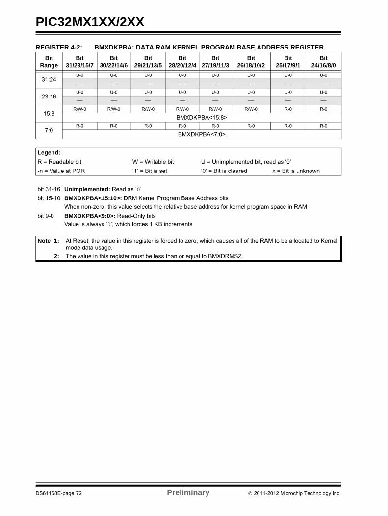
PIC32MX1XX/2XX
REGISTER 4-2: BMXDKPBA: DATA RAM KERNEL PROGRAM BASE ADDRESS REGISTER
Bit Range
Bit31/23/15/7
Bit30/22/14/6
Bit29/21/13/5
Bit28/20/12/4
Bit27/19/11/3
Bit26/18/10/2
Bit25/17/9/1
Bit24/16/8/0
31:24U-0 U-0 U-0 U-0 U-0 U-0 U-0 U-0
— — — — — — — —
23:16U-0 U-0 U-0 U-0 U-0 U-0 U-0 U-0
— — — — — — — —
15:8R/W-0 R/W-0 R/W-0 R/W-0 R/W-0 R/W-0 R-0 R-0
BMXDKPBA<15:8>
7:0R-0 R-0 R-0 R-0 R-0 R-0 R-0 R-0
BMXDKPBA<7:0>
Legend:
R = Readable bit W = Writable bit U = Unimplemented bit, read as ‘0’
-n = Value at POR ‘1’ = Bit is set ‘0’ = Bit is cleared x = Bit is unknown
bit 31-16 Unimplemented: Read as ‘0’
bit 15-10 BMXDKPBA<15:10>: DRM Kernel Program Base Address bits
When non-zero, this value selects the relative base address for kernel program space in RAM
bit 9-0 BMXDKPBA<9:0>: Read-Only bits
Value is always ‘0’, which forces 1 KB increments
Note 1: At Reset, the value in this register is forced to zero, which causes all of the RAM to be allocated to Kernal mode data usage.
2: The value in this register must be less than or equal to BMXDRMSZ.
DS61168E-page 72 Preliminary 2011-2012 Microchip Technology Inc.
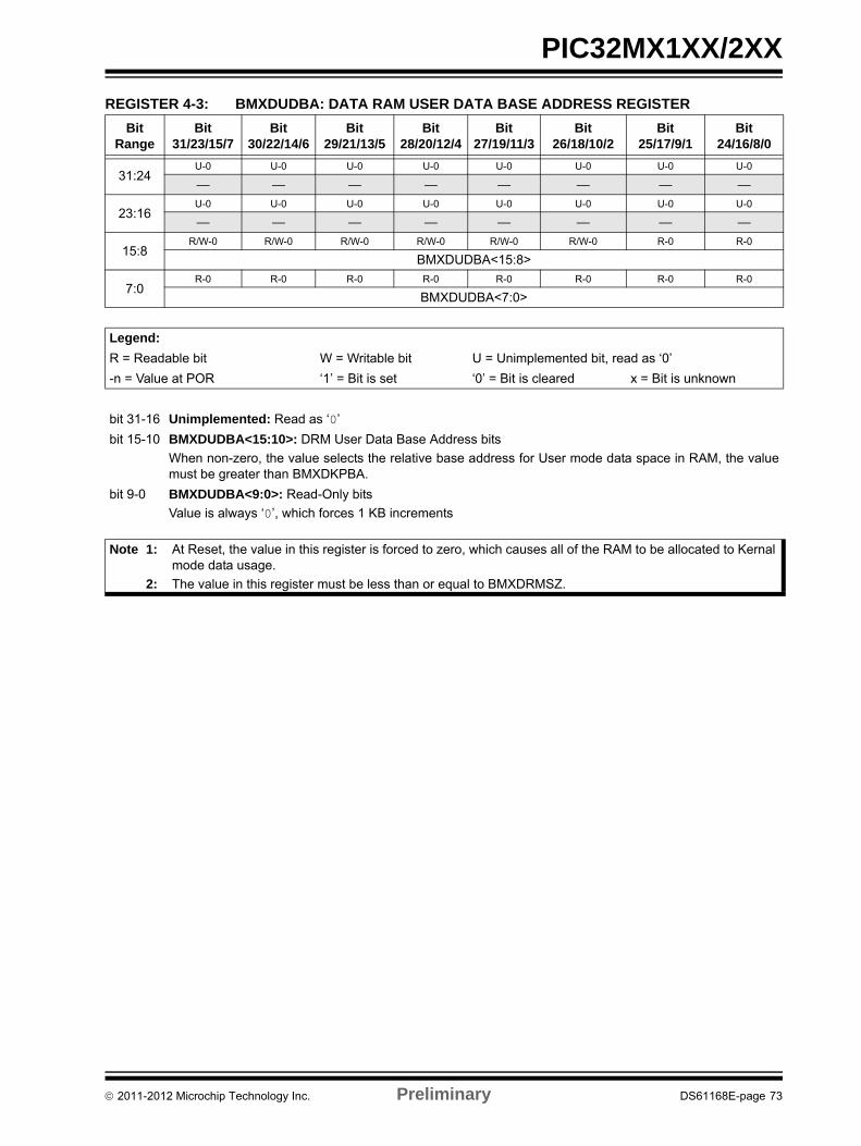
PIC32MX1XX/2XX
REGISTER 4-3: BMXDUDBA: DATA RAM USER DATA BASE ADDRESS REGISTER
Bit Range
Bit31/23/15/7
Bit30/22/14/6
Bit29/21/13/5
Bit28/20/12/4
Bit27/19/11/3
Bit26/18/10/2
Bit25/17/9/1
Bit24/16/8/0
31:24U-0 U-0 U-0 U-0 U-0 U-0 U-0 U-0
— — — — — — — —
23:16U-0 U-0 U-0 U-0 U-0 U-0 U-0 U-0
— — — — — — — —
15:8R/W-0 R/W-0 R/W-0 R/W-0 R/W-0 R/W-0 R-0 R-0
BMXDUDBA<15:8>
7:0R-0 R-0 R-0 R-0 R-0 R-0 R-0 R-0
BMXDUDBA<7:0>
Legend:
R = Readable bit W = Writable bit U = Unimplemented bit, read as ‘0’
-n = Value at POR ‘1’ = Bit is set ‘0’ = Bit is cleared x = Bit is unknown
bit 31-16 Unimplemented: Read as ‘0’
bit 15-10 BMXDUDBA<15:10>: DRM User Data Base Address bits
When non-zero, the value selects the relative base address for User mode data space in RAM, the valuemust be greater than BMXDKPBA.
bit 9-0 BMXDUDBA<9:0>: Read-Only bits
Value is always ‘0’, which forces 1 KB increments
Note 1: At Reset, the value in this register is forced to zero, which causes all of the RAM to be allocated to Kernal mode data usage.
2: The value in this register must be less than or equal to BMXDRMSZ.
2011-2012 Microchip Technology Inc. Preliminary DS61168E-page 73
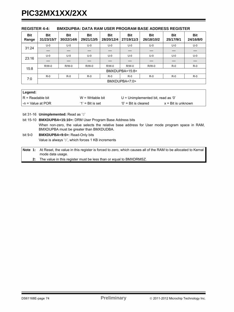
PIC32MX1XX/2XX
REGISTER 4-4: BMXDUPBA: DATA RAM USER PROGRAM BASE ADDRESS REGISTER
Bit Range
Bit31/23/15/7
Bit30/22/14/6
Bit29/21/13/5
Bit28/20/12/4
Bit27/19/11/3
Bit26/18/10/2
Bit25/17/9/1
Bit24/16/8/0
31:24U-0 U-0 U-0 U-0 U-0 U-0 U-0 U-0
— — — — — — — —
23:16U-0 U-0 U-0 U-0 U-0 U-0 U-0 U-0
— — — — — — — —
15:8R/W-0 R/W-0 R/W-0 R/W-0 R/W-0 R/W-0 R-0 R-0
BMXDUPBA<15:8>
7:0R-0 R-0 R-0 R-0 R-0 R-0 R-0 R-0
BMXDUPBA<7:0>
Legend:
R = Readable bit W = Writable bit U = Unimplemented bit, read as ‘0’
-n = Value at POR ‘1’ = Bit is set ‘0’ = Bit is cleared x = Bit is unknown
bit 31-16 Unimplemented: Read as ‘0’
bit 15-10 BMXDUPBA<15:10>: DRM User Program Base Address bits
When non-zero, the value selects the relative base address for User mode program space in RAM,BMXDUPBA must be greater than BMXDUDBA.
bit 9-0 BMXDUPBA<9:0>: Read-Only bits
Value is always ‘0’, which forces 1 KB increments
Note 1: At Reset, the value in this register is forced to zero, which causes all of the RAM to be allocated to Kernal mode data usage.
2: The value in this register must be less than or equal to BMXDRMSZ.
DS61168E-page 74 Preliminary 2011-2012 Microchip Technology Inc.
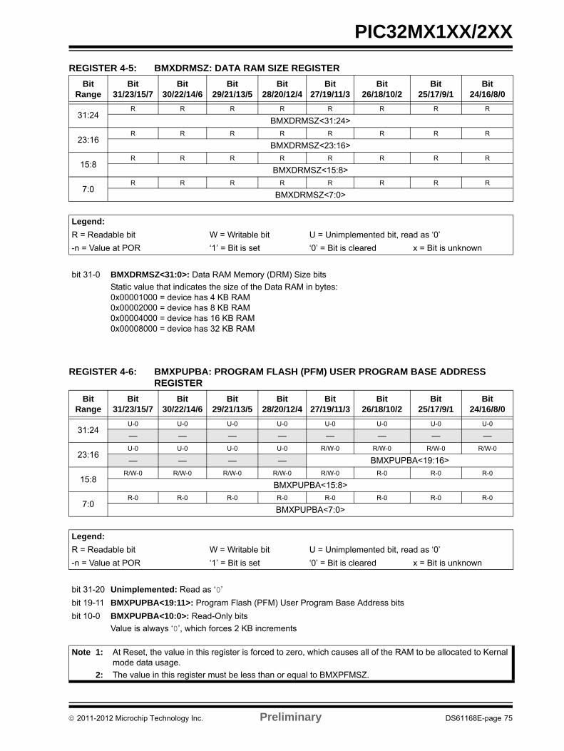
PIC32MX1XX/2XX
REGISTER 4-5: BMXDRMSZ: DATA RAM SIZE REGISTER
Bit Range
Bit31/23/15/7
Bit30/22/14/6
Bit29/21/13/5
Bit28/20/12/4
Bit27/19/11/3
Bit26/18/10/2
Bit25/17/9/1
Bit24/16/8/0
31:24R R R R R R R R
BMXDRMSZ<31:24>
23:16R R R R R R R R
BMXDRMSZ<23:16>
15:8R R R R R R R R
BMXDRMSZ<15:8>
7:0R R R R R R R R
BMXDRMSZ<7:0>
Legend:
R = Readable bit W = Writable bit U = Unimplemented bit, read as ‘0’
-n = Value at POR ‘1’ = Bit is set ‘0’ = Bit is cleared x = Bit is unknown
bit 31-0 BMXDRMSZ<31:0>: Data RAM Memory (DRM) Size bits
Static value that indicates the size of the Data RAM in bytes:0x00001000 = device has 4 KB RAM0x00002000 = device has 8 KB RAM0x00004000 = device has 16 KB RAM0x00008000 = device has 32 KB RAM
REGISTER 4-6: BMXPUPBA: PROGRAM FLASH (PFM) USER PROGRAM BASE ADDRESS REGISTER
Bit Range
Bit31/23/15/7
Bit30/22/14/6
Bit29/21/13/5
Bit28/20/12/4
Bit27/19/11/3
Bit26/18/10/2
Bit25/17/9/1
Bit24/16/8/0
31:24U-0 U-0 U-0 U-0 U-0 U-0 U-0 U-0
— — — — — — — —
23:16U-0 U-0 U-0 U-0 R/W-0 R/W-0 R/W-0 R/W-0
— — — — BMXPUPBA<19:16>
15:8R/W-0 R/W-0 R/W-0 R/W-0 R/W-0 R-0 R-0 R-0
BMXPUPBA<15:8>
7:0R-0 R-0 R-0 R-0 R-0 R-0 R-0 R-0
BMXPUPBA<7:0>
Legend:
R = Readable bit W = Writable bit U = Unimplemented bit, read as ‘0’
-n = Value at POR ‘1’ = Bit is set ‘0’ = Bit is cleared x = Bit is unknown
bit 31-20 Unimplemented: Read as ‘0’
bit 19-11 BMXPUPBA<19:11>: Program Flash (PFM) User Program Base Address bits
bit 10-0 BMXPUPBA<10:0>: Read-Only bits
Value is always ‘0’, which forces 2 KB increments
Note 1: At Reset, the value in this register is forced to zero, which causes all of the RAM to be allocated to Kernal mode data usage.
2: The value in this register must be less than or equal to BMXPFMSZ.
2011-2012 Microchip Technology Inc. Preliminary DS61168E-page 75
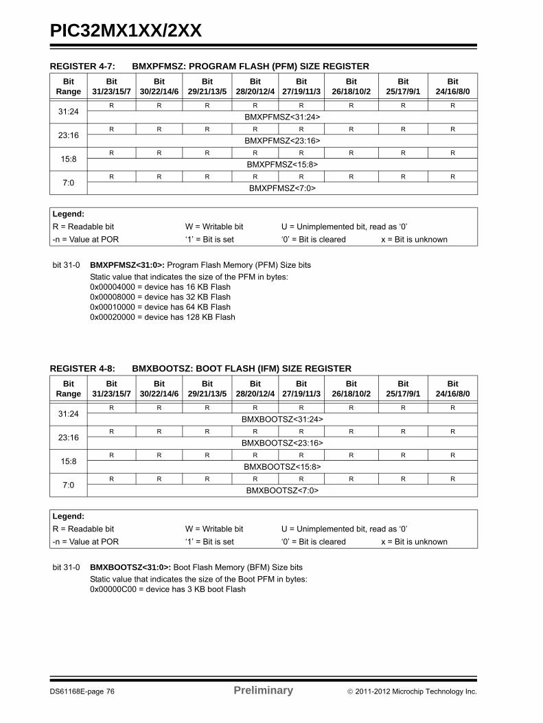
PIC32MX1XX/2XX
REGISTER 4-7: BMXPFMSZ: PROGRAM FLASH (PFM) SIZE REGISTER
Bit Range
Bit31/23/15/7
Bit30/22/14/6
Bit29/21/13/5
Bit28/20/12/4
Bit27/19/11/3
Bit26/18/10/2
Bit25/17/9/1
Bit24/16/8/0
31:24R R R R R R R R
BMXPFMSZ<31:24>
23:16R R R R R R R R
BMXPFMSZ<23:16>
15:8R R R R R R R R
BMXPFMSZ<15:8>
7:0R R R R R R R R
BMXPFMSZ<7:0>
Legend:
R = Readable bit W = Writable bit U = Unimplemented bit, read as ‘0’
-n = Value at POR ‘1’ = Bit is set ‘0’ = Bit is cleared x = Bit is unknown
bit 31-0 BMXPFMSZ<31:0>: Program Flash Memory (PFM) Size bits
Static value that indicates the size of the PFM in bytes:0x00004000 = device has 16 KB Flash0x00008000 = device has 32 KB Flash0x00010000 = device has 64 KB Flash0x00020000 = device has 128 KB Flash
REGISTER 4-8: BMXBOOTSZ: BOOT FLASH (IFM) SIZE REGISTER
Bit Range
Bit31/23/15/7
Bit30/22/14/6
Bit29/21/13/5
Bit28/20/12/4
Bit27/19/11/3
Bit26/18/10/2
Bit25/17/9/1
Bit24/16/8/0
31:24R R R R R R R R
BMXBOOTSZ<31:24>
23:16R R R R R R R R
BMXBOOTSZ<23:16>
15:8R R R R R R R R
BMXBOOTSZ<15:8>
7:0R R R R R R R R
BMXBOOTSZ<7:0>
Legend:
R = Readable bit W = Writable bit U = Unimplemented bit, read as ‘0’
-n = Value at POR ‘1’ = Bit is set ‘0’ = Bit is cleared x = Bit is unknown
bit 31-0 BMXBOOTSZ<31:0>: Boot Flash Memory (BFM) Size bits
Static value that indicates the size of the Boot PFM in bytes:0x00000C00 = device has 3 KB boot Flash
DS61168E-page 76 Preliminary 2011-2012 Microchip Technology Inc.
PIC32MX1XX/2XX
5.0 FLASH PROGRAM MEMORY
PIC32MX1XX/2XX devices contain an internal Flashprogram memory for executing user code. There arethree methods by which the user can program thismemory:
• Run-Time Self-Programming (RTSP)
• EJTAG Programming
• In-Circuit Serial Programming™ (ICSP™)
RTSP is performed by software executing from eitherFlash or RAM memory. Information about RTSPtechniques is available in Section 5. “Flash ProgramMemory” (DS61121) in the “PIC32 Family ReferenceManual”.
EJTAG is performed using the EJTAG port of thedevice and an EJTAG capable programmer.
ICSP is performed using a serial data connection to thedevice and allows much faster programming times thanRTSP.
The EJTAG and ICSP methods are described in the“PIC32 Flash Programming Specification” (DS61145),which can be downloaded from the Microchip web site.
Note 1: This data sheet summarizes the featuresof the PIC32MX1XX/2XX family ofdevices. It is not intended to be acomprehensive reference source. Tocomplement the information in this datasheet, refer to Section 5. “FlashProgram Memory” (DS61121) in the“PIC32 Family Reference Manual”, whichis available from the Microchip web site(www.microchip.com/PIC32).
2: Some registers and associated bitsdescribed in this section may not beavailable on all devices. Refer toSection 4.0 “Memory Organization” inthis data sheet for device-specific registerand bit information.
Note: The Flash page size onPIC32MX1XX/2XX devices is 1 KB andthe row size is 128 bytes (256 IW and 32IW, respectively).
2011-2012 Microchip Technology Inc. Preliminary DS61168E-page 77
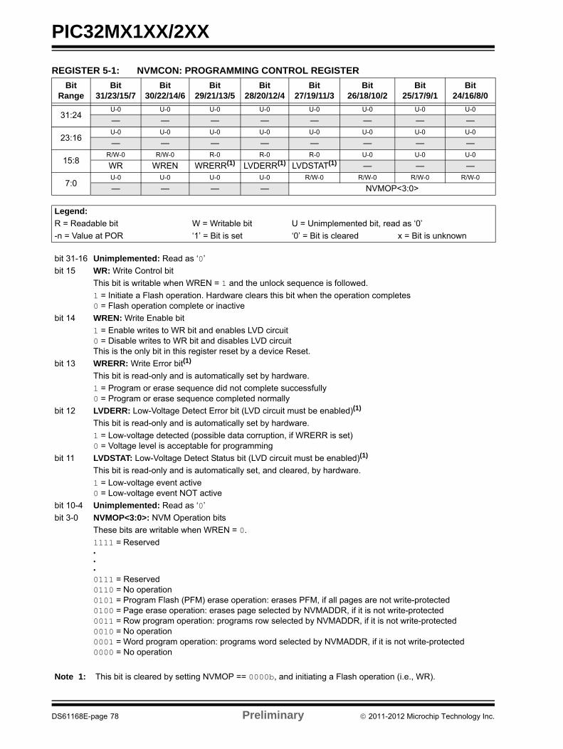
PIC32MX1XX/2XX
REGISTER 5-1: NVMCON: PROGRAMMING CONTROL REGISTER
Bit Range
Bit31/23/15/7
Bit30/22/14/6
Bit29/21/13/5
Bit28/20/12/4
Bit27/19/11/3
Bit26/18/10/2
Bit25/17/9/1
Bit24/16/8/0
31:24U-0 U-0 U-0 U-0 U-0 U-0 U-0 U-0
— — — — — — — —
23:16U-0 U-0 U-0 U-0 U-0 U-0 U-0 U-0
— — — — — — — —
15:8R/W-0 R/W-0 R-0 R-0 R-0 U-0 U-0 U-0
WR WREN WRERR(1) LVDERR(1) LVDSTAT(1) — — —
7:0U-0 U-0 U-0 U-0 R/W-0 R/W-0 R/W-0 R/W-0
— — — — NVMOP<3:0>
Legend:
R = Readable bit W = Writable bit U = Unimplemented bit, read as ‘0’
-n = Value at POR ‘1’ = Bit is set ‘0’ = Bit is cleared x = Bit is unknown
bit 31-16 Unimplemented: Read as ‘0’
bit 15 WR: Write Control bit
This bit is writable when WREN = 1 and the unlock sequence is followed.
1 = Initiate a Flash operation. Hardware clears this bit when the operation completes0 = Flash operation complete or inactive
bit 14 WREN: Write Enable bit
1 = Enable writes to WR bit and enables LVD circuit0 = Disable writes to WR bit and disables LVD circuitThis is the only bit in this register reset by a device Reset.
bit 13 WRERR: Write Error bit(1)
This bit is read-only and is automatically set by hardware.
1 = Program or erase sequence did not complete successfully0 = Program or erase sequence completed normally
bit 12 LVDERR: Low-Voltage Detect Error bit (LVD circuit must be enabled)(1)
This bit is read-only and is automatically set by hardware.
1 = Low-voltage detected (possible data corruption, if WRERR is set)0 = Voltage level is acceptable for programming
bit 11 LVDSTAT: Low-Voltage Detect Status bit (LVD circuit must be enabled)(1)
This bit is read-only and is automatically set, and cleared, by hardware.
1 = Low-voltage event active0 = Low-voltage event NOT active
bit 10-4 Unimplemented: Read as ‘0’
bit 3-0 NVMOP<3:0>: NVM Operation bits
These bits are writable when WREN = 0.
1111 = Reserved•••
0111 = Reserved0110 = No operation0101 = Program Flash (PFM) erase operation: erases PFM, if all pages are not write-protected0100 = Page erase operation: erases page selected by NVMADDR, if it is not write-protected0011 = Row program operation: programs row selected by NVMADDR, if it is not write-protected0010 = No operation0001 = Word program operation: programs word selected by NVMADDR, if it is not write-protected0000 = No operation
Note 1: This bit is cleared by setting NVMOP == 0000b, and initiating a Flash operation (i.e., WR).
DS61168E-page 78 Preliminary 2011-2012 Microchip Technology Inc.
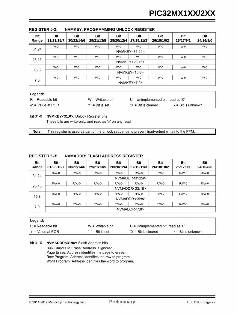
PIC32MX1XX/2XX
REGISTER 5-2: NVMKEY: PROGRAMMING UNLOCK REGISTER
Bit Range
Bit31/23/15/7
Bit30/22/14/6
Bit29/21/13/5
Bit28/20/12/4
Bit27/19/11/3
Bit26/18/10/2
Bit25/17/9/1
Bit24/16/8/0
31:24W-0 W-0 W-0 W-0 W-0 W-0 W-0 W-0
NVMKEY<31:24>
23:16W-0 W-0 W-0 W-0 W-0 W-0 W-0 W-0
NVMKEY<23:16>
15:8W-0 W-0 W-0 W-0 W-0 W-0 W-0 W-0
NVMKEY<15:8>
7:0W-0 W-0 W-0 W-0 W-0 W-0 W-0 W-0
NVMKEY<7:0>
Legend:
R = Readable bit W = Writable bit U = Unimplemented bit, read as ‘0’
-n = Value at POR ‘1’ = Bit is set ‘0’ = Bit is cleared x = Bit is unknown
bit 31-0 NVMKEY<31:0>: Unlock Register bits
These bits are write-only, and read as ‘0’ on any read
Note: This register is used as part of the unlock sequence to prevent inadvertent writes to the PFM.
REGISTER 5-3: NVMADDR: FLASH ADDRESS REGISTER
Bit Range
Bit31/23/15/7
Bit30/22/14/6
Bit29/21/13/5
Bit28/20/12/4
Bit27/19/11/3
Bit26/18/10/2
Bit25/17/9/1
Bit24/16/8/0
31:24R/W-0 R/W-0 R/W-0 R/W-0 R/W-0 R/W-0 R/W-0 R/W-0
NVMADDR<31:24>
23:16R/W-0 R/W-0 R/W-0 R/W-0 R/W-0 R/W-0 R/W-0 R/W-0
NVMADDR<23:16>
15:8R/W-0 R/W-0 R/W-0 R/W-0 R/W-0 R/W-0 R/W-0 R/W-0
NVMADDR<15:8>
7:0R/W-0 R/W-0 R/W-0 R/W-0 R/W-0 R/W-0 R/W-0 R/W-0
NVMADDR<7:0>
Legend:
R = Readable bit W = Writable bit U = Unimplemented bit, read as ‘0’
-n = Value at POR ‘1’ = Bit is set ‘0’ = Bit is cleared x = Bit is unknown
bit 31-0 NVMADDR<31:0>: Flash Address bits
Bulk/Chip/PFM Erase: Address is ignored.Page Erase: Address identifies the page to erase.Row Program: Address identifies the row to program.Word Program: Address identifies the word to program.
2011-2012 Microchip Technology Inc. Preliminary DS61168E-page 79
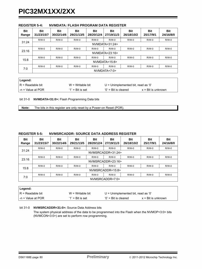
PIC32MX1XX/2XX
REGISTER 5-4: NVMDATA: FLASH PROGRAM DATA REGISTER
Bit Range
Bit31/23/15/7
Bit30/22/14/6
Bit29/21/13/5
Bit28/20/12/4
Bit27/19/11/3
Bit26/18/10/2
Bit25/17/9/1
Bit24/16/8/0
31:24R/W-0 R/W-0 R/W-0 R/W-0 R/W-0 R/W-0 R/W-0 R/W-0
NVMDATA<31:24>
23:16R/W-0 R/W-0 R/W-0 R/W-0 R/W-0 R/W-0 R/W-0 R/W-0
NVMDATA<23:16>
15:8R/W-0 R/W-0 R/W-0 R/W-0 R/W-0 R/W-0 R/W-0 R/W-0
NVMDATA<15:8>
7:0R/W-0 R/W-0 R/W-0 R/W-0 R/W-0 R/W-0 R/W-0 R/W-0
NVMDATA<7:0>
Legend:
R = Readable bit W = Writable bit U = Unimplemented bit, read as ‘0’
-n = Value at POR ‘1’ = Bit is set ‘0’ = Bit is cleared x = Bit is unknown
bit 31-0 NVMDATA<31:0>: Flash Programming Data bits
Note: The bits in this register are only reset by a Power-on Reset (POR).
REGISTER 5-5: NVMSRCADDR: SOURCE DATA ADDRESS REGISTER
Bit Range
Bit31/23/15/7
Bit30/22/14/6
Bit29/21/13/5
Bit28/20/12/4
Bit27/19/11/3
Bit26/18/10/2
Bit25/17/9/1
Bit24/16/8/0
31:24R/W-0 R/W-0 R/W-0 R/W-0 R/W-0 R/W-0 R/W-0 R/W-0
NVMSRCADDR<31:24>
23:16R/W-0 R/W-0 R/W-0 R/W-0 R/W-0 R/W-0 R/W-0 R/W-0
NVMSRCADDR<23:16>
15:8R/W-0 R/W-0 R/W-0 R/W-0 R/W-0 R/W-0 R/W-0 R/W-0
NVMSRCADDR<15:8>
7:0R/W-0 R/W-0 R/W-0 R/W-0 R/W-0 R/W-0 R/W-0 R/W-0
NVMSRCADDR<7:0>
Legend:
R = Readable bit W = Writable bit U = Unimplemented bit, read as ‘0’
-n = Value at POR ‘1’ = Bit is set ‘0’ = Bit is cleared x = Bit is unknown
bit 31-0 NVMSRCADDR<31:0>: Source Data Address bits
The system physical address of the data to be programmed into the Flash when the NVMOP<3:0> bits (NVMCON<3:0>) are set to perform row programming.
DS61168E-page 80 Preliminary 2011-2012 Microchip Technology Inc.
PIC32MX1XX/2XX
6.0 RESETS The Reset module combines all Reset sources andcontrols the device Master Reset signal, SYSRST. Thefollowing is a list of device Reset sources:
• POR: Power-on Reset
• MCLR: Master Clear Reset pin
• SWR: Software Reset
• WDTR: Watchdog Timer Reset
• BOR: Brown-out Reset
• CMR: Configuration Mismatch Reset
A simplified block diagram of the Reset module isillustrated in Figure 6-1.
FIGURE 6-1: SYSTEM RESET BLOCK DIAGRAM
Note 1: This data sheet summarizes the featuresof the PIC32MX1XX/2XX family ofdevices. It is not intended to be acomprehensive reference source. Tocomplement the information in this datasheet, refer to Section 7. “Resets”(DS61118) in the “PIC32 FamilyReference Manual”, which is availablefrom the Microchip web site(www.microchip.com/PIC32).
2: Some registers and associated bitsdescribed in this section may not beavailable on all devices. Refer toSection 4.0 “Memory Organization” inthis data sheet for device-specific registerand bit information.
MCLR
VDDVDD Rise
Detect
POR
Sleep or Idle
Brown-outReset
WDTTime-out
Glitch Filter
BOR
Configuration
SYSRST
Software Reset
Power-upTimer
Voltage
Enabled
Reset
WDTR
SWR
CMR
MCLR
Mismatch
Regulator
2011-2012 Microchip Technology Inc. Preliminary DS61168E-page 81
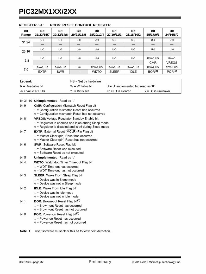
PIC32MX1XX/2XX
REGISTER 6-1: RCON: RESET CONTROL REGISTER
Bit Range
Bit31/23/15/7
Bit30/22/14/6
Bit29/21/13/5
Bit28/20/12/4
Bit27/19/11/3
Bit26/18/10/2
Bit25/17/9/1
Bit24/16/8/0
31:24U-0 U-0 U-0 U-0 U-0 U-0 U-0 U-0
— — — — — — — —
23:16U-0 U-0 U-0 U-0 U-0 U-0 U-0 U-0
— — — — — — — —
15:8U-0 U-0 U-0 U-0 U-0 U-0 R/W-0, HS R/W-0
— — — — — — CMR VREGS
7:0R/W-0, HS R/W-0, HS U-0 R/W-0, HS R/W-0, HS R/W-0, HS R/W-1, HS R/W-1, HS
EXTR SWR — WDTO SLEEP IDLE BOR(1) POR(1)
Legend: HS = Set by hardware
R = Readable bit W = Writable bit U = Unimplemented bit, read as ‘0’
-n = Value at POR ‘1’ = Bit is set ‘0’ = Bit is cleared x = Bit is unknown
bit 31-10 Unimplemented: Read as ‘0’
bit 9 CMR: Configuration Mismatch Reset Flag bit 1 = Configuration mismatch Reset has occurred0 = Configuration mismatch Reset has not occurred
bit 8 VREGS: Voltage Regulator Standby Enable bit1 = Regulator is enabled and is on during Sleep mode0 = Regulator is disabled and is off during Sleep mode
bit 7 EXTR: External Reset (MCLR) Pin Flag bit1 = Master Clear (pin) Reset has occurred0 = Master Clear (pin) Reset has not occurred
bit 6 SWR: Software Reset Flag bit1 = Software Reset was executed0 = Software Reset as not executed
bit 5 Unimplemented: Read as ‘0’
bit 4 WDTO: Watchdog Timer Time-out Flag bit1 = WDT Time-out has occurred0 = WDT Time-out has not occurred
bit 3 SLEEP: Wake From Sleep Flag bit1 = Device was in Sleep mode0 = Device was not in Sleep mode
bit 2 IDLE: Wake From Idle Flag bit1 = Device was in Idle mode0 = Device was not in Idle mode
bit 1 BOR: Brown-out Reset Flag bit(1)
1 = Brown-out Reset has occurred 0 = Brown-out Reset has not occurred
bit 0 POR: Power-on Reset Flag bit(1)
1 = Power-on Reset has occurred0 = Power-on Reset has not occurred
Note 1: User software must clear this bit to view next detection.
DS61168E-page 82 Preliminary 2011-2012 Microchip Technology Inc.
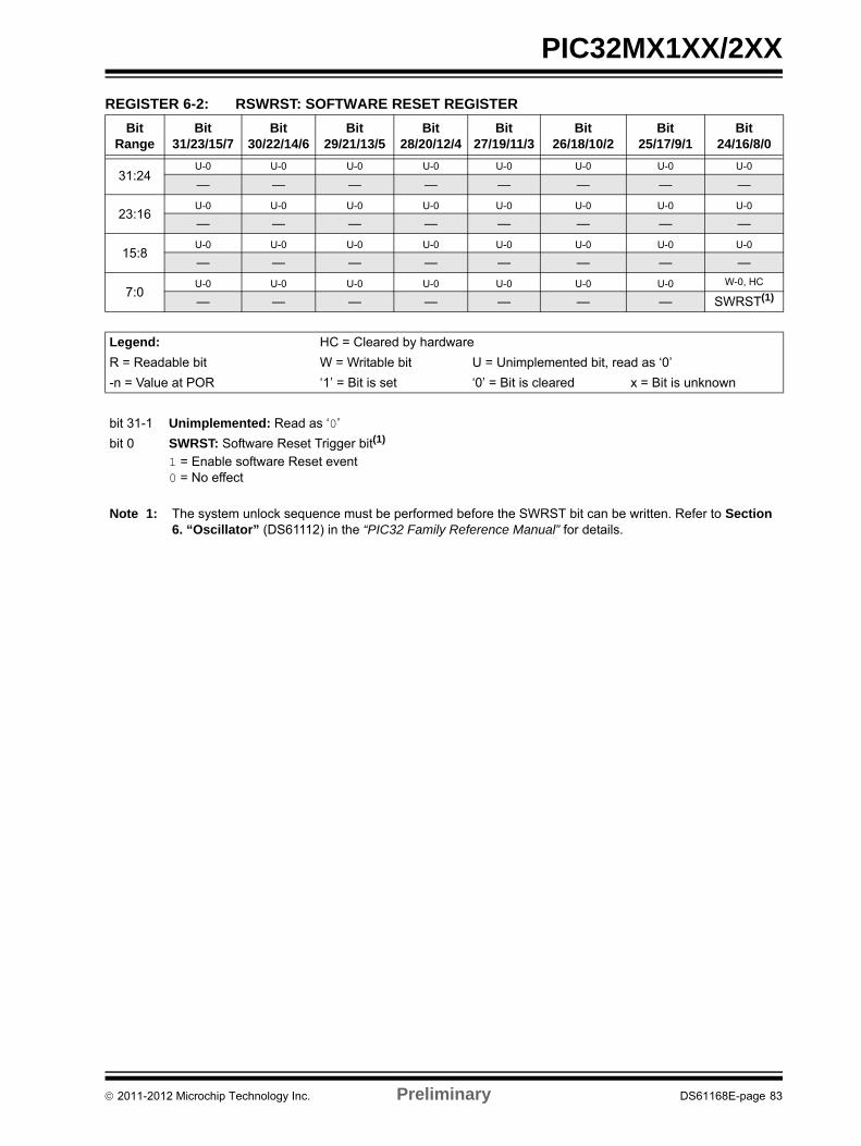
PIC32MX1XX/2XX
REGISTER 6-2: RSWRST: SOFTWARE RESET REGISTER
Bit Range
Bit31/23/15/7
Bit30/22/14/6
Bit29/21/13/5
Bit28/20/12/4
Bit27/19/11/3
Bit26/18/10/2
Bit25/17/9/1
Bit24/16/8/0
31:24U-0 U-0 U-0 U-0 U-0 U-0 U-0 U-0
— — — — — — — —
23:16U-0 U-0 U-0 U-0 U-0 U-0 U-0 U-0
— — — — — — — —
15:8U-0 U-0 U-0 U-0 U-0 U-0 U-0 U-0
— — — — — — — —
7:0U-0 U-0 U-0 U-0 U-0 U-0 U-0 W-0, HC
— — — — — — — SWRST(1)
Legend: HC = Cleared by hardware
R = Readable bit W = Writable bit U = Unimplemented bit, read as ‘0’
-n = Value at POR ‘1’ = Bit is set ‘0’ = Bit is cleared x = Bit is unknown
bit 31-1 Unimplemented: Read as ‘0’
bit 0 SWRST: Software Reset Trigger bit(1)
1 = Enable software Reset event0 = No effect
Note 1: The system unlock sequence must be performed before the SWRST bit can be written. Refer to Section 6. “Oscillator” (DS61112) in the “PIC32 Family Reference Manual” for details.
2011-2012 Microchip Technology Inc. Preliminary DS61168E-page 83

PIC32MX1XX/2XX
NOTES:
DS61168E-page 84 Preliminary 2011-2012 Microchip Technology Inc.
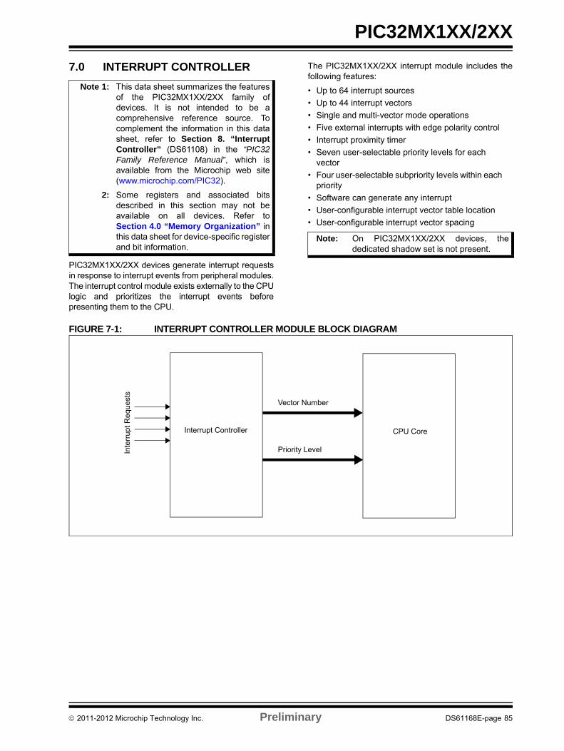
PIC32MX1XX/2XX
7.0 INTERRUPT CONTROLLER
PIC32MX1XX/2XX devices generate interrupt requestsin response to interrupt events from peripheral modules.The interrupt control module exists externally to the CPUlogic and prioritizes the interrupt events beforepresenting them to the CPU.
The PIC32MX1XX/2XX interrupt module includes thefollowing features:
• Up to 64 interrupt sources
• Up to 44 interrupt vectors
• Single and multi-vector mode operations
• Five external interrupts with edge polarity control
• Interrupt proximity timer
• Seven user-selectable priority levels for each vector
• Four user-selectable subpriority levels within each priority
• Software can generate any interrupt
• User-configurable interrupt vector table location
• User-configurable interrupt vector spacing
FIGURE 7-1: INTERRUPT CONTROLLER MODULE BLOCK DIAGRAM
Note 1: This data sheet summarizes the featuresof the PIC32MX1XX/2XX family ofdevices. It is not intended to be acomprehensive reference source. Tocomplement the information in this datasheet, refer to Section 8. “InterruptController” (DS61108) in the “PIC32Family Reference Manual”, which isavailable from the Microchip web site(www.microchip.com/PIC32).
2: Some registers and associated bitsdescribed in this section may not beavailable on all devices. Refer toSection 4.0 “Memory Organization” inthis data sheet for device-specific registerand bit information.
Note: On PIC32MX1XX/2XX devices, thededicated shadow set is not present.
Interrupt Controller
Inte
rrup
t Re
ques
ts
Vector Number
CPU Core
Priority Level
2011-2012 Microchip Technology Inc. Preliminary DS61168E-page 85
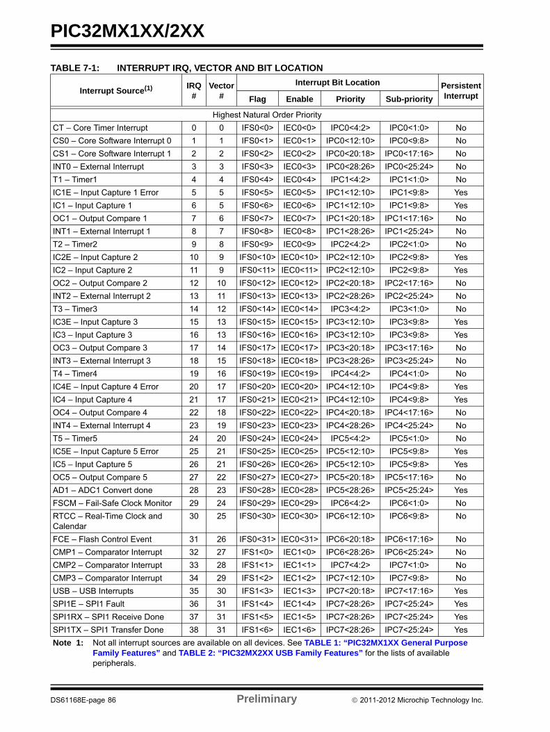
PIC32MX1XX/2XX
TABLE 7-1: INTERRUPT IRQ, VECTOR AND BIT LOCATION
Interrupt Source(1) IRQ #
Vector #
Interrupt Bit Location Persistent InterruptFlag Enable Priority Sub-priority
Highest Natural Order Priority
CT – Core Timer Interrupt 0 0 IFS0<0> IEC0<0> IPC0<4:2> IPC0<1:0> No
CS0 – Core Software Interrupt 0 1 1 IFS0<1> IEC0<1> IPC0<12:10> IPC0<9:8> No
CS1 – Core Software Interrupt 1 2 2 IFS0<2> IEC0<2> IPC0<20:18> IPC0<17:16> No
INT0 – External Interrupt 3 3 IFS0<3> IEC0<3> IPC0<28:26> IPC0<25:24> No
T1 – Timer1 4 4 IFS0<4> IEC0<4> IPC1<4:2> IPC1<1:0> No
IC1E – Input Capture 1 Error 5 5 IFS0<5> IEC0<5> IPC1<12:10> IPC1<9:8> Yes
IC1 – Input Capture 1 6 5 IFS0<6> IEC0<6> IPC1<12:10> IPC1<9:8> Yes
OC1 – Output Compare 1 7 6 IFS0<7> IEC0<7> IPC1<20:18> IPC1<17:16> No
INT1 – External Interrupt 1 8 7 IFS0<8> IEC0<8> IPC1<28:26> IPC1<25:24> No
T2 – Timer2 9 8 IFS0<9> IEC0<9> IPC2<4:2> IPC2<1:0> No
IC2E – Input Capture 2 10 9 IFS0<10> IEC0<10> IPC2<12:10> IPC2<9:8> Yes
IC2 – Input Capture 2 11 9 IFS0<11> IEC0<11> IPC2<12:10> IPC2<9:8> Yes
OC2 – Output Compare 2 12 10 IFS0<12> IEC0<12> IPC2<20:18> IPC2<17:16> No
INT2 – External Interrupt 2 13 11 IFS0<13> IEC0<13> IPC2<28:26> IPC2<25:24> No
T3 – Timer3 14 12 IFS0<14> IEC0<14> IPC3<4:2> IPC3<1:0> No
IC3E – Input Capture 3 15 13 IFS0<15> IEC0<15> IPC3<12:10> IPC3<9:8> Yes
IC3 – Input Capture 3 16 13 IFS0<16> IEC0<16> IPC3<12:10> IPC3<9:8> Yes
OC3 – Output Compare 3 17 14 IFS0<17> IEC0<17> IPC3<20:18> IPC3<17:16> No
INT3 – External Interrupt 3 18 15 IFS0<18> IEC0<18> IPC3<28:26> IPC3<25:24> No
T4 – Timer4 19 16 IFS0<19> IEC0<19> IPC4<4:2> IPC4<1:0> No
IC4E – Input Capture 4 Error 20 17 IFS0<20> IEC0<20> IPC4<12:10> IPC4<9:8> Yes
IC4 – Input Capture 4 21 17 IFS0<21> IEC0<21> IPC4<12:10> IPC4<9:8> Yes
OC4 – Output Compare 4 22 18 IFS0<22> IEC0<22> IPC4<20:18> IPC4<17:16> No
INT4 – External Interrupt 4 23 19 IFS0<23> IEC0<23> IPC4<28:26> IPC4<25:24> No
T5 – Timer5 24 20 IFS0<24> IEC0<24> IPC5<4:2> IPC5<1:0> No
IC5E – Input Capture 5 Error 25 21 IFS0<25> IEC0<25> IPC5<12:10> IPC5<9:8> Yes
IC5 – Input Capture 5 26 21 IFS0<26> IEC0<26> IPC5<12:10> IPC5<9:8> Yes
OC5 – Output Compare 5 27 22 IFS0<27> IEC0<27> IPC5<20:18> IPC5<17:16> No
AD1 – ADC1 Convert done 28 23 IFS0<28> IEC0<28> IPC5<28:26> IPC5<25:24> Yes
FSCM – Fail-Safe Clock Monitor 29 24 IFS0<29> IEC0<29> IPC6<4:2> IPC6<1:0> No
RTCC – Real-Time Clock and Calendar
30 25 IFS0<30> IEC0<30> IPC6<12:10> IPC6<9:8> No
FCE – Flash Control Event 31 26 IFS0<31> IEC0<31> IPC6<20:18> IPC6<17:16> No
CMP1 – Comparator Interrupt 32 27 IFS1<0> IEC1<0> IPC6<28:26> IPC6<25:24> No
CMP2 – Comparator Interrupt 33 28 IFS1<1> IEC1<1> IPC7<4:2> IPC7<1:0> No
CMP3 – Comparator Interrupt 34 29 IFS1<2> IEC1<2> IPC7<12:10> IPC7<9:8> No
USB – USB Interrupts 35 30 IFS1<3> IEC1<3> IPC7<20:18> IPC7<17:16> Yes
SPI1E – SPI1 Fault 36 31 IFS1<4> IEC1<4> IPC7<28:26> IPC7<25:24> Yes
SPI1RX – SPI1 Receive Done 37 31 IFS1<5> IEC1<5> IPC7<28:26> IPC7<25:24> Yes
SPI1TX – SPI1 Transfer Done 38 31 IFS1<6> IEC1<6> IPC7<28:26> IPC7<25:24> Yes
Note 1: Not all interrupt sources are available on all devices. See TABLE 1: “PIC32MX1XX General Purpose Family Features” and TABLE 2: “PIC32MX2XX USB Family Features” for the lists of available peripherals.
DS61168E-page 86 Preliminary 2011-2012 Microchip Technology Inc.
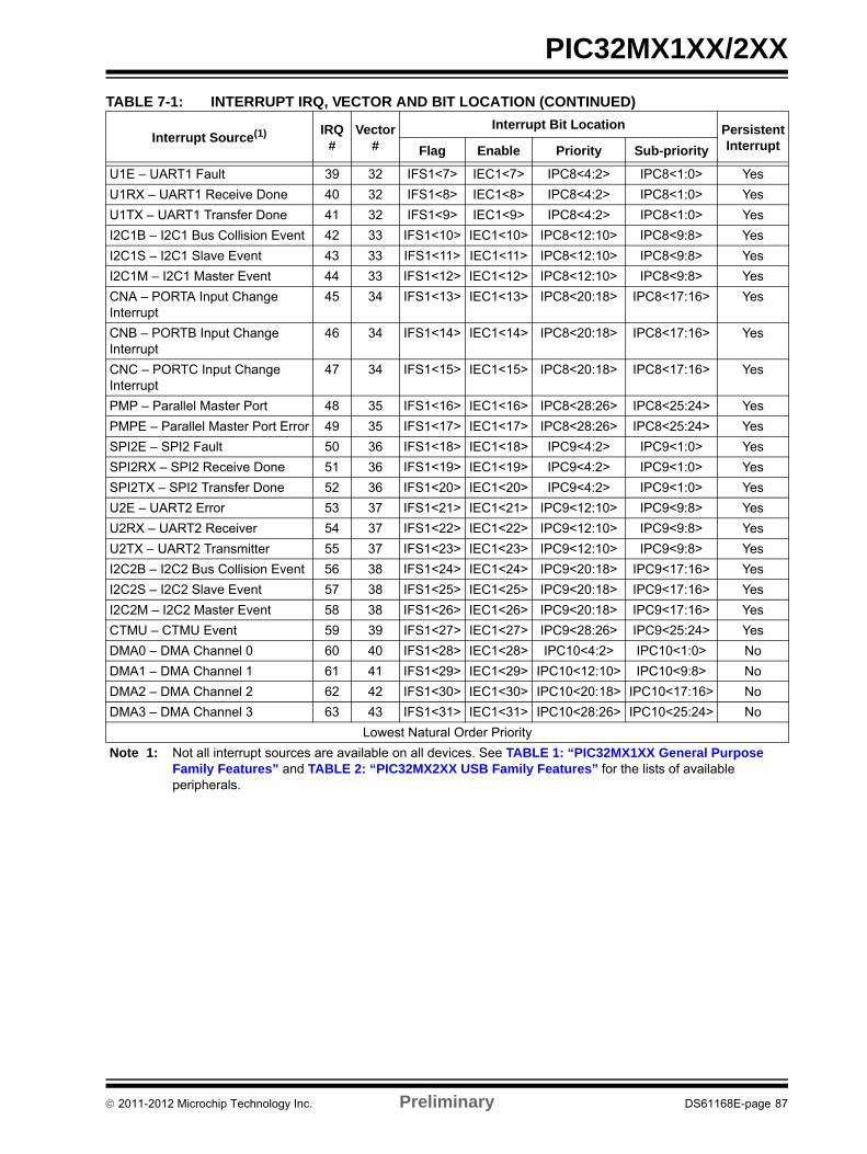
PIC32MX1XX/2XX
U1E – UART1 Fault 39 32 IFS1<7> IEC1<7> IPC8<4:2> IPC8<1:0> Yes
U1RX – UART1 Receive Done 40 32 IFS1<8> IEC1<8> IPC8<4:2> IPC8<1:0> Yes
U1TX – UART1 Transfer Done 41 32 IFS1<9> IEC1<9> IPC8<4:2> IPC8<1:0> Yes
I2C1B – I2C1 Bus Collision Event 42 33 IFS1<10> IEC1<10> IPC8<12:10> IPC8<9:8> Yes
I2C1S – I2C1 Slave Event 43 33 IFS1<11> IEC1<11> IPC8<12:10> IPC8<9:8> Yes
I2C1M – I2C1 Master Event 44 33 IFS1<12> IEC1<12> IPC8<12:10> IPC8<9:8> Yes
CNA – PORTA Input Change Interrupt
45 34 IFS1<13> IEC1<13> IPC8<20:18> IPC8<17:16> Yes
CNB – PORTB Input Change Interrupt
46 34 IFS1<14> IEC1<14> IPC8<20:18> IPC8<17:16> Yes
CNC – PORTC Input Change Interrupt
47 34 IFS1<15> IEC1<15> IPC8<20:18> IPC8<17:16> Yes
PMP – Parallel Master Port 48 35 IFS1<16> IEC1<16> IPC8<28:26> IPC8<25:24> Yes
PMPE – Parallel Master Port Error 49 35 IFS1<17> IEC1<17> IPC8<28:26> IPC8<25:24> Yes
SPI2E – SPI2 Fault 50 36 IFS1<18> IEC1<18> IPC9<4:2> IPC9<1:0> Yes
SPI2RX – SPI2 Receive Done 51 36 IFS1<19> IEC1<19> IPC9<4:2> IPC9<1:0> Yes
SPI2TX – SPI2 Transfer Done 52 36 IFS1<20> IEC1<20> IPC9<4:2> IPC9<1:0> Yes
U2E – UART2 Error 53 37 IFS1<21> IEC1<21> IPC9<12:10> IPC9<9:8> Yes
U2RX – UART2 Receiver 54 37 IFS1<22> IEC1<22> IPC9<12:10> IPC9<9:8> Yes
U2TX – UART2 Transmitter 55 37 IFS1<23> IEC1<23> IPC9<12:10> IPC9<9:8> Yes
I2C2B – I2C2 Bus Collision Event 56 38 IFS1<24> IEC1<24> IPC9<20:18> IPC9<17:16> Yes
I2C2S – I2C2 Slave Event 57 38 IFS1<25> IEC1<25> IPC9<20:18> IPC9<17:16> Yes
I2C2M – I2C2 Master Event 58 38 IFS1<26> IEC1<26> IPC9<20:18> IPC9<17:16> Yes
CTMU – CTMU Event 59 39 IFS1<27> IEC1<27> IPC9<28:26> IPC9<25:24> Yes
DMA0 – DMA Channel 0 60 40 IFS1<28> IEC1<28> IPC10<4:2> IPC10<1:0> No
DMA1 – DMA Channel 1 61 41 IFS1<29> IEC1<29> IPC10<12:10> IPC10<9:8> No
DMA2 – DMA Channel 2 62 42 IFS1<30> IEC1<30> IPC10<20:18> IPC10<17:16> No
DMA3 – DMA Channel 3 63 43 IFS1<31> IEC1<31> IPC10<28:26> IPC10<25:24> No
Lowest Natural Order Priority
TABLE 7-1: INTERRUPT IRQ, VECTOR AND BIT LOCATION (CONTINUED)
Interrupt Source(1) IRQ #
Vector #
Interrupt Bit Location Persistent InterruptFlag Enable Priority Sub-priority
Note 1: Not all interrupt sources are available on all devices. See TABLE 1: “PIC32MX1XX General Purpose Family Features” and TABLE 2: “PIC32MX2XX USB Family Features” for the lists of available peripherals.
2011-2012 Microchip Technology Inc. Preliminary DS61168E-page 87
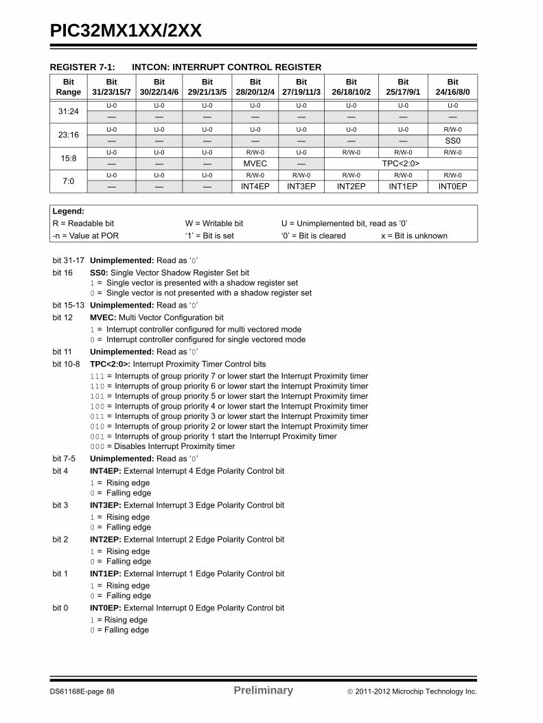
PIC32MX1XX/2XX
REGISTER 7-1: INTCON: INTERRUPT CONTROL REGISTER
Bit Range
Bit31/23/15/7
Bit30/22/14/6
Bit29/21/13/5
Bit28/20/12/4
Bit27/19/11/3
Bit26/18/10/2
Bit25/17/9/1
Bit24/16/8/0
31:24U-0 U-0 U-0 U-0 U-0 U-0 U-0 U-0
— — — — — — — —
23:16U-0 U-0 U-0 U-0 U-0 U-0 U-0 R/W-0
— — — — — — — SS0
15:8U-0 U-0 U-0 R/W-0 U-0 R/W-0 R/W-0 R/W-0
— — — MVEC — TPC<2:0>
7:0U-0 U-0 U-0 R/W-0 R/W-0 R/W-0 R/W-0 R/W-0
— — — INT4EP INT3EP INT2EP INT1EP INT0EP
Legend:
R = Readable bit W = Writable bit U = Unimplemented bit, read as ‘0’
-n = Value at POR ‘1’ = Bit is set ‘0’ = Bit is cleared x = Bit is unknown
bit 31-17 Unimplemented: Read as ‘0’
bit 16 SS0: Single Vector Shadow Register Set bit1 = Single vector is presented with a shadow register set0 = Single vector is not presented with a shadow register set
bit 15-13 Unimplemented: Read as ‘0’
bit 12 MVEC: Multi Vector Configuration bit
1 = Interrupt controller configured for multi vectored mode0 = Interrupt controller configured for single vectored mode
bit 11 Unimplemented: Read as ‘0’
bit 10-8 TPC<2:0>: Interrupt Proximity Timer Control bits
111 = Interrupts of group priority 7 or lower start the Interrupt Proximity timer110 = Interrupts of group priority 6 or lower start the Interrupt Proximity timer101 = Interrupts of group priority 5 or lower start the Interrupt Proximity timer100 = Interrupts of group priority 4 or lower start the Interrupt Proximity timer011 = Interrupts of group priority 3 or lower start the Interrupt Proximity timer010 = Interrupts of group priority 2 or lower start the Interrupt Proximity timer001 = Interrupts of group priority 1 start the Interrupt Proximity timer000 = Disables Interrupt Proximity timer
bit 7-5 Unimplemented: Read as ‘0’
bit 4 INT4EP: External Interrupt 4 Edge Polarity Control bit
1 = Rising edge0 = Falling edge
bit 3 INT3EP: External Interrupt 3 Edge Polarity Control bit
1 = Rising edge0 = Falling edge
bit 2 INT2EP: External Interrupt 2 Edge Polarity Control bit
1 = Rising edge0 = Falling edge
bit 1 INT1EP: External Interrupt 1 Edge Polarity Control bit
1 = Rising edge0 = Falling edge
bit 0 INT0EP: External Interrupt 0 Edge Polarity Control bit
1 = Rising edge0 = Falling edge
DS61168E-page 88 Preliminary 2011-2012 Microchip Technology Inc.
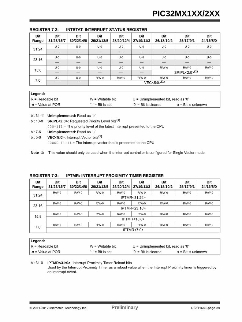
PIC32MX1XX/2XX
REGISTER 7-2: INTSTAT: INTERRUPT STATUS REGISTER
Bit Range
Bit31/23/15/7
Bit30/22/14/6
Bit29/21/13/5
Bit28/20/12/4
Bit27/19/11/3
Bit26/18/10/2
Bit25/17/9/1
Bit24/16/8/0
31:24U-0 U-0 U-0 U-0 U-0 U-0 U-0 U-0
— — — — — — — —
23:16U-0 U-0 U-0 U-0 U-0 U-0 U-0 U-0
— — — — — — — —
15:8U-0 U-0 U-0 U-0 U-0 R/W-0 R/W-0 R/W-0
— — — — — SRIPL<2:0>(1)
7:0U-0 U-0 R/W-0 R/W-0 R/W-0 R/W-0 R/W-0 R/W-0
— — VEC<5:0>(1)
Legend:
R = Readable bit W = Writable bit U = Unimplemented bit, read as ‘0’
-n = Value at POR ‘1’ = Bit is set ‘0’ = Bit is cleared x = Bit is unknown
bit 31-11 Unimplemented: Read as ‘0’
bit 10-8 SRIPL<2:0>: Requested Priority Level bits(1)
000-111 = The priority level of the latest interrupt presented to the CPU
bit 7-6 Unimplemented: Read as ‘0’
bit 5-0 VEC<5:0>: Interrupt Vector bits(1)
00000-11111 = The interrupt vector that is presented to the CPU
Note 1: This value should only be used when the interrupt controller is configured for Single Vector mode.
REGISTER 7-3: IPTMR: INTERRUPT PROXIMITY TIMER REGISTER
Bit Range
Bit31/23/15/7
Bit30/22/14/6
Bit29/21/13/5
Bit28/20/12/4
Bit27/19/11/3
Bit26/18/10/2
Bit25/17/9/1
Bit24/16/8/0
31:24R/W-0 R/W-0 R/W-0 R/W-0 R/W-0 R/W-0 R/W-0 R/W-0
IPTMR<31:24>
23:16R/W-0 R/W-0 R/W-0 R/W-0 R/W-0 R/W-0 R/W-0 R/W-0
IPTMR<23:16>
15:8R/W-0 R/W-0 R/W-0 R/W-0 R/W-0 R/W-0 R/W-0 R/W-0
IPTMR<15:8>
7:0R/W-0 R/W-0 R/W-0 R/W-0 R/W-0 R/W-0 R/W-0 R/W-0
IPTMR<7:0>
Legend:
R = Readable bit W = Writable bit U = Unimplemented bit, read as ‘0’
-n = Value at POR ‘1’ = Bit is set ‘0’ = Bit is cleared x = Bit is unknown
bit 31-0 IPTMR<31:0>: Interrupt Proximity Timer Reload bitsUsed by the Interrupt Proximity Timer as a reload value when the Interrupt Proximity timer is triggered by an interrupt event.
2011-2012 Microchip Technology Inc. Preliminary DS61168E-page 89
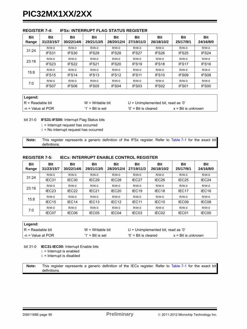
PIC32MX1XX/2XX
REGISTER 7-4: IFSx: INTERRUPT FLAG STATUS REGISTER
Bit Range
Bit31/23/15/7
Bit30/22/14/6
Bit29/21/13/5
Bit28/20/12/4
Bit27/19/11/3
Bit26/18/10/2
Bit25/17/9/1
Bit24/16/8/0
31:24R/W-0 R/W-0 R/W-0 R/W-0 R/W-0 R/W-0 R/W-0 R/W-0
IFS31 IFS30 IFS29 IFS28 IFS27 IFS26 IFS25 IFS24
23:16R/W-0 R/W-0 R/W-0 R/W-0 R/W-0 R/W-0 R/W-0 R/W-0
IFS23 IFS22 IFS21 IFS20 IFS19 IFS18 IFS17 IFS16
15:8R/W-0 R/W-0 R/W-0 R/W-0 R/W-0 R/W-0 R/W-0 R/W-0
IFS15 IFS14 IFS13 IFS12 IFS11 IFS10 IFS09 IFS08
7:0R/W-0 R/W-0 R/W-0 R/W-0 R/W-0 R/W-0 R/W-0 R/W-0
IFS07 IFS06 IFS05 IFS04 IFS03 IFS02 IFS01 IFS00
Legend:
R = Readable bit W = Writable bit U = Unimplemented bit, read as ‘0’
-n = Value at POR ‘1’ = Bit is set ‘0’ = Bit is cleared x = Bit is unknown
bit 31-0 IFS31-IFS00: Interrupt Flag Status bits
1 = Interrupt request has occurred0 = No interrupt request has occurred
Note: This register represents a generic definition of the IFSx register. Refer to Table 7-1 for the exact bitdefinitions.
REGISTER 7-5: IECx: INTERRUPT ENABLE CONTROL REGISTER
Bit Range
Bit31/23/15/7
Bit30/22/14/6
Bit29/21/13/5
Bit28/20/12/4
Bit27/19/11/3
Bit26/18/10/2
Bit25/17/9/1
Bit24/16/8/0
31:24R/W-0 R/W-0 R/W-0 R/W-0 R/W-0 R/W-0 R/W-0 R/W-0
IEC31 IEC30 IEC29 IEC28 IEC27 IEC26 IEC25 IEC24
23:16R/W-0 R/W-0 R/W-0 R/W-0 R/W-0 R/W-0 R/W-0 R/W-0
IEC23 IEC22 IEC21 IEC20 IEC19 IEC18 IEC17 IEC16
15:8R/W-0 R/W-0 R/W-0 R/W-0 R/W-0 R/W-0 R/W-0 R/W-0
IEC15 IEC14 IEC13 IEC12 IEC11 IEC10 IEC09 IEC08
7:0R/W-0 R/W-0 R/W-0 R/W-0 R/W-0 R/W-0 R/W-0 R/W-0
IEC07 IEC06 IEC05 IEC04 IEC03 IEC02 IEC01 IEC00
Legend:
R = Readable bit W = Writable bit U = Unimplemented bit, read as ‘0’
-n = Value at POR ‘1’ = Bit is set ‘0’ = Bit is cleared x = Bit is unknown
bit 31-0 IEC31-IEC00: Interrupt Enable bits1 = Interrupt is enabled0 = Interrupt is disabled
Note: This register represents a generic definition of the IECx register. Refer to Table 7-1 for the exact bitdefinitions.
DS61168E-page 90 Preliminary 2011-2012 Microchip Technology Inc.
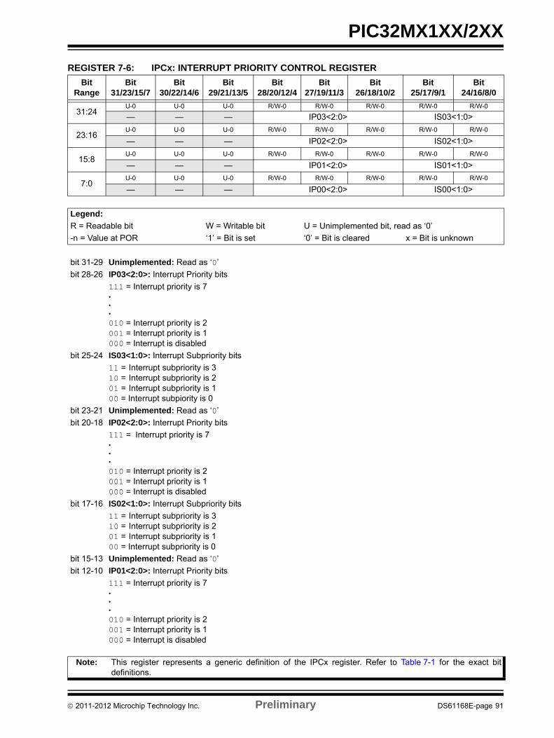
PIC32MX1XX/2XX
REGISTER 7-6: IPCx: INTERRUPT PRIORITY CONTROL REGISTER
Bit Range
Bit31/23/15/7
Bit30/22/14/6
Bit29/21/13/5
Bit28/20/12/4
Bit27/19/11/3
Bit26/18/10/2
Bit25/17/9/1
Bit24/16/8/0
31:24U-0 U-0 U-0 R/W-0 R/W-0 R/W-0 R/W-0 R/W-0
— — — IP03<2:0> IS03<1:0>
23:16U-0 U-0 U-0 R/W-0 R/W-0 R/W-0 R/W-0 R/W-0
— — — IP02<2:0> IS02<1:0>
15:8U-0 U-0 U-0 R/W-0 R/W-0 R/W-0 R/W-0 R/W-0
— — — IP01<2:0> IS01<1:0>
7:0U-0 U-0 U-0 R/W-0 R/W-0 R/W-0 R/W-0 R/W-0
— — — IP00<2:0> IS00<1:0>
Legend:
R = Readable bit W = Writable bit U = Unimplemented bit, read as ‘0’
-n = Value at POR ‘1’ = Bit is set ‘0’ = Bit is cleared x = Bit is unknown
bit 31-29 Unimplemented: Read as ‘0’
bit 28-26 IP03<2:0>: Interrupt Priority bits
111 = Interrupt priority is 7•••
010 = Interrupt priority is 2001 = Interrupt priority is 1000 = Interrupt is disabled
bit 25-24 IS03<1:0>: Interrupt Subpriority bits
11 = Interrupt subpriority is 310 = Interrupt subpriority is 201 = Interrupt subpriority is 100 = Interrupt subpiority is 0
bit 23-21 Unimplemented: Read as ‘0’
bit 20-18 IP02<2:0>: Interrupt Priority bits
111 = Interrupt priority is 7•••
010 = Interrupt priority is 2001 = Interrupt priority is 1000 = Interrupt is disabled
bit 17-16 IS02<1:0>: Interrupt Subpriority bits
11 = Interrupt subpriority is 310 = Interrupt subpriority is 201 = Interrupt subpriority is 100 = Interrupt subpriority is 0
bit 15-13 Unimplemented: Read as ‘0’
bit 12-10 IP01<2:0>: Interrupt Priority bits
111 = Interrupt priority is 7•••
010 = Interrupt priority is 2001 = Interrupt priority is 1000 = Interrupt is disabled
Note: This register represents a generic definition of the IPCx register. Refer to Table 7-1 for the exact bitdefinitions.
2011-2012 Microchip Technology Inc. Preliminary DS61168E-page 91
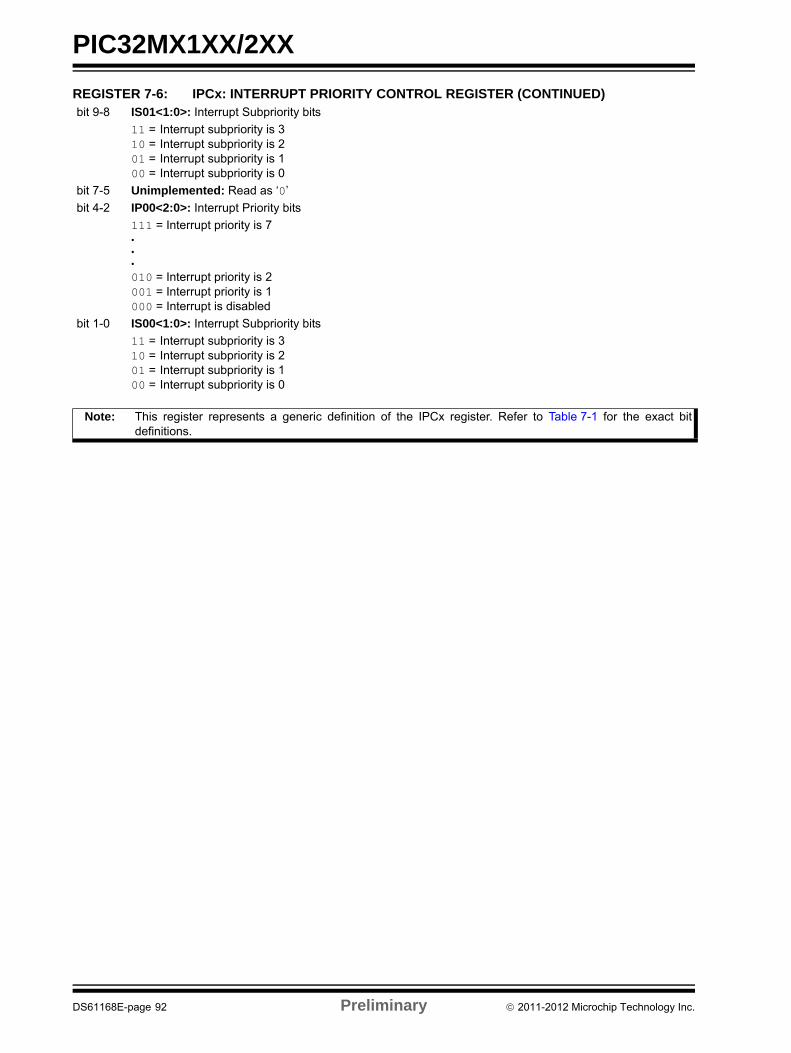
PIC32MX1XX/2XX
bit 9-8 IS01<1:0>: Interrupt Subpriority bits
11 = Interrupt subpriority is 310 = Interrupt subpriority is 201 = Interrupt subpriority is 100 = Interrupt subpriority is 0
bit 7-5 Unimplemented: Read as ‘0’
bit 4-2 IP00<2:0>: Interrupt Priority bits
111 = Interrupt priority is 7•••
010 = Interrupt priority is 2001 = Interrupt priority is 1000 = Interrupt is disabled
bit 1-0 IS00<1:0>: Interrupt Subpriority bits
11 = Interrupt subpriority is 310 = Interrupt subpriority is 201 = Interrupt subpriority is 100 = Interrupt subpriority is 0
REGISTER 7-6: IPCx: INTERRUPT PRIORITY CONTROL REGISTER (CONTINUED)
Note: This register represents a generic definition of the IPCx register. Refer to Table 7-1 for the exact bitdefinitions.
DS61168E-page 92 Preliminary 2011-2012 Microchip Technology Inc.
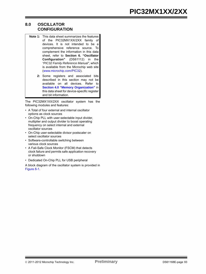
PIC32MX1XX/2XX
8.0 OSCILLATOR CONFIGURATION
The PIC32MX1XX/2XX oscillator system has thefollowing modules and features:
• A Total of four external and internal oscillator options as clock sources
• On-Chip PLL with user-selectable input divider, multiplier and output divider to boost operating frequency on select internal and external oscillator sources
• On-Chip user-selectable divisor postscaler on select oscillator sources
• Software-controllable switching between various clock sources
• A Fail-Safe Clock Monitor (FSCM) that detects clock failure and permits safe application recovery or shutdown
• Dedicated On-Chip PLL for USB peripheral
A block diagram of the oscillator system is provided inFigure 8-1.
Note 1: This data sheet summarizes the featuresof the PIC32MX1XX/2XX family ofdevices. It is not intended to be acomprehensive reference source. Tocomplement the information in this datasheet, refer to Section 6. “OscillatorConfiguration” (DS61112) in the“PIC32 Family Reference Manual”, whichis available from the Microchip web site(www.microchip.com/PIC32).
2: Some registers and associated bitsdescribed in this section may not beavailable on all devices. Refer toSection 4.0 “Memory Organization” inthis data sheet for device-specific registerand bit information.
2011-2012 Microchip Technology Inc. Preliminary DS61168E-page 93
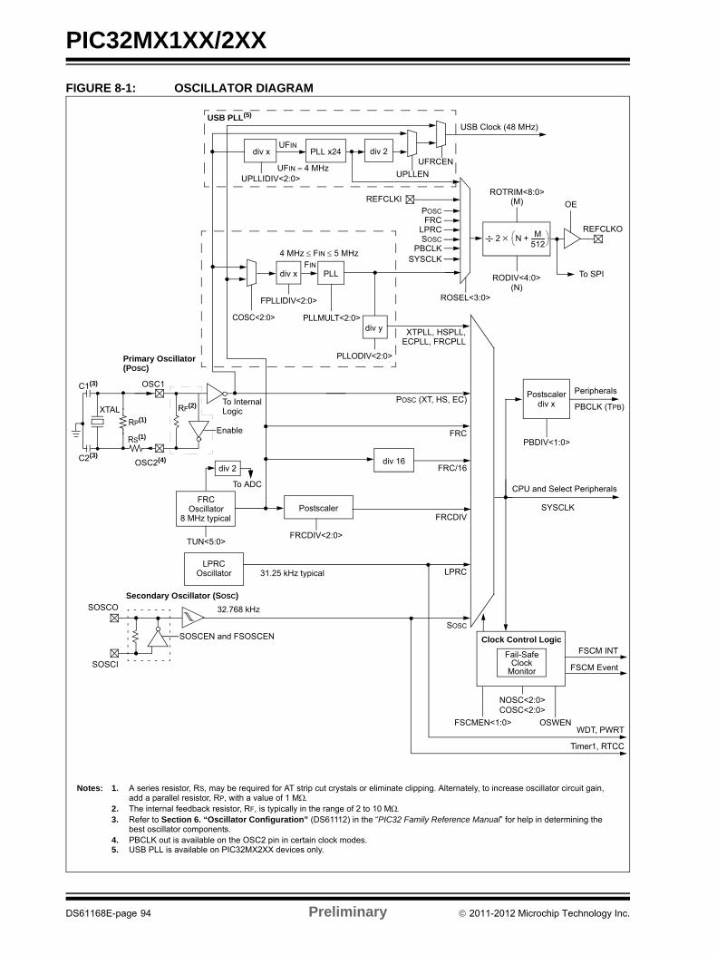
PIC32MX1XX/2XX
FIGURE 8-1: OSCILLATOR DIAGRAM
Timer1, RTCC
Clock Control Logic
Fail-SafeClock
Monitor
FSCM INT
FSCM Event
COSC<2:0>NOSC<2:0>
OSWENFSCMEN<1:0>
PLL
Secondary Oscillator (SOSC)
SOSCEN and FSOSCEN
SOSCO
SOSCI
Primary Oscillator
POSC (XT, HS, EC)
CPU and Select Peripherals
Peripherals
FRCDIV<2:0>
WDT, PWRT
8 MHz typical
FRC
31.25 kHz typical
FRCOscillator
LPRCOscillator
SOSC
LPRC
FRCDIV
TUN<5:0>
div 16
Postscaler
FPLLIDIV<2:0>
PBDIV<1:0>
FRC/16
Postscaler
COSC<2:0>
FINdiv x
div y
PLLODIV<2:0>
div x
32.768 kHz
PLLMULT<2:0>
PBCLK (TPB)
UFIN 4 MHz
PLL x24
USB Clock (48 MHz)
div 2
UPLLEN
UFRCENdiv x
UPLLIDIV<2:0>
UFIN
4 MHz FIN 5 MHz
C1(3)
C2(3)
XTAL
RS(1)Enable
Notes: 1. A series resistor, RS, may be required for AT strip cut crystals or eliminate clipping. Alternately, to increase oscillator circuit gain, add a parallel resistor, RP, with a value of 1 M
2. The internal feedback resistor, RF, is typically in the range of 2 to 10 M3. Refer to Section 6. “Oscillator Configuration” (DS61112) in the “PIC32 Family Reference Manual” for help in determining the
best oscillator components.4. PBCLK out is available on the OSC2 pin in certain clock modes.5. USB PLL is available on PIC32MX2XX devices only.
OSC2(4)
OSC1
RF(2) To InternalLogic
USB PLL(5)
(POSC)
div 2
To ADC
SYSCLK
REFCLKI
REFCLKO
OE
To SPI
ROSEL<3:0>
POSC
FRCLPRCSOSC
PBCLKSYSCLK
XTPLL, HSPLL,ECPLL, FRCPLL
2 N M512----------+
RODIV<4:0>(N)
ROTRIM<8:0>(M)
RP(1)
DS61168E-page 94 Preliminary 2011-2012 Microchip Technology Inc.
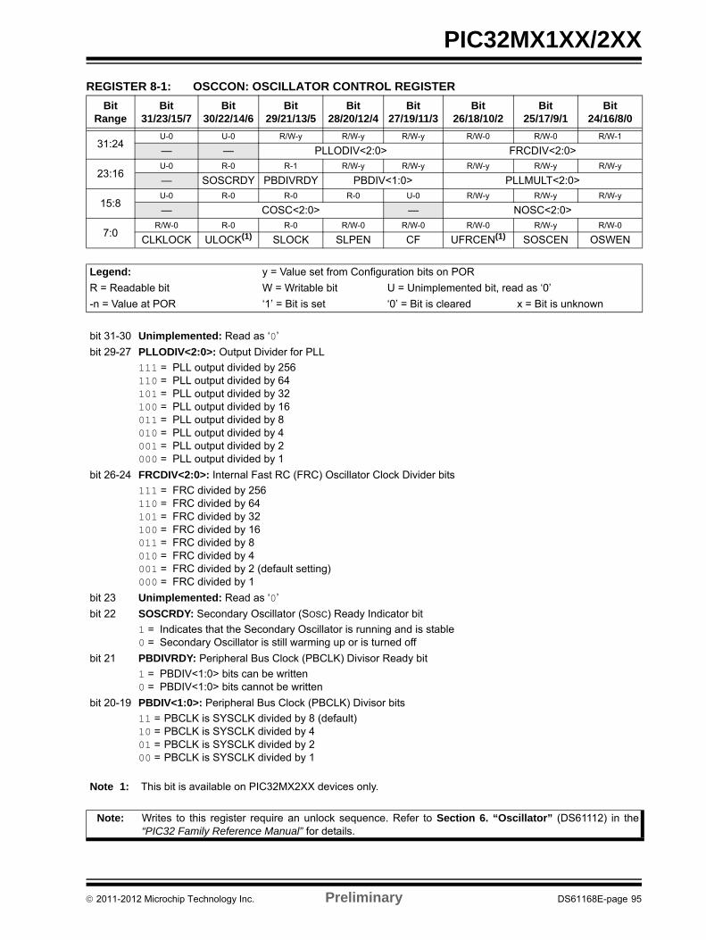
PIC32MX1XX/2XX
REGISTER 8-1: OSCCON: OSCILLATOR CONTROL REGISTER
Bit Range
Bit31/23/15/7
Bit30/22/14/6
Bit29/21/13/5
Bit28/20/12/4
Bit27/19/11/3
Bit26/18/10/2
Bit25/17/9/1
Bit24/16/8/0
31:24U-0 U-0 R/W-y R/W-y R/W-y R/W-0 R/W-0 R/W-1
— — PLLODIV<2:0> FRCDIV<2:0>
23:16U-0 R-0 R-1 R/W-y R/W-y R/W-y R/W-y R/W-y
— SOSCRDY PBDIVRDY PBDIV<1:0> PLLMULT<2:0>
15:8U-0 R-0 R-0 R-0 U-0 R/W-y R/W-y R/W-y
— COSC<2:0> — NOSC<2:0>
7:0R/W-0 R-0 R-0 R/W-0 R/W-0 R/W-0 R/W-y R/W-0
CLKLOCK ULOCK(1) SLOCK SLPEN CF UFRCEN(1) SOSCEN OSWEN
Legend: y = Value set from Configuration bits on POR
R = Readable bit W = Writable bit U = Unimplemented bit, read as ‘0’
-n = Value at POR ‘1’ = Bit is set ‘0’ = Bit is cleared x = Bit is unknown
bit 31-30 Unimplemented: Read as ‘0’
bit 29-27 PLLODIV<2:0>: Output Divider for PLL
111 = PLL output divided by 256110 = PLL output divided by 64101 = PLL output divided by 32100 = PLL output divided by 16011 = PLL output divided by 8010 = PLL output divided by 4001 = PLL output divided by 2000 = PLL output divided by 1
bit 26-24 FRCDIV<2:0>: Internal Fast RC (FRC) Oscillator Clock Divider bits
111 = FRC divided by 256110 = FRC divided by 64101 = FRC divided by 32100 = FRC divided by 16011 = FRC divided by 8010 = FRC divided by 4001 = FRC divided by 2 (default setting)000 = FRC divided by 1
bit 23 Unimplemented: Read as ‘0’
bit 22 SOSCRDY: Secondary Oscillator (SOSC) Ready Indicator bit
1 = Indicates that the Secondary Oscillator is running and is stable0 = Secondary Oscillator is still warming up or is turned off
bit 21 PBDIVRDY: Peripheral Bus Clock (PBCLK) Divisor Ready bit
1 = PBDIV<1:0> bits can be written0 = PBDIV<1:0> bits cannot be written
bit 20-19 PBDIV<1:0>: Peripheral Bus Clock (PBCLK) Divisor bits
11 = PBCLK is SYSCLK divided by 8 (default)10 = PBCLK is SYSCLK divided by 401 = PBCLK is SYSCLK divided by 200 = PBCLK is SYSCLK divided by 1
Note 1: This bit is available on PIC32MX2XX devices only.
Note: Writes to this register require an unlock sequence. Refer to Section 6. “Oscillator” (DS61112) in the“PIC32 Family Reference Manual” for details.
2011-2012 Microchip Technology Inc. Preliminary DS61168E-page 95
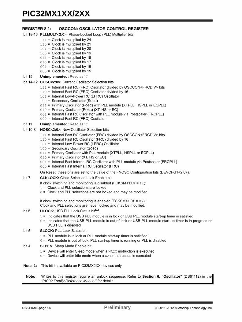
PIC32MX1XX/2XX
bit 18-16 PLLMULT<2:0>: Phase-Locked Loop (PLL) Multiplier bits
111 = Clock is multiplied by 24110 = Clock is multiplied by 21101 = Clock is multiplied by 20100 = Clock is multiplied by 19011 = Clock is multiplied by 18010 = Clock is multiplied by 17001 = Clock is multiplied by 16000 = Clock is multiplied by 15
bit 15 Unimplemented: Read as ‘0’
bit 14-12 COSC<2:0>: Current Oscillator Selection bits
111 = Internal Fast RC (FRC) Oscillator divided by OSCCON<FRCDIV> bits110 = Internal Fast RC (FRC) Oscillator divided by 16101 = Internal Low-Power RC (LPRC) Oscillator100 = Secondary Oscillator (SOSC)011 = Primary Oscillator (POSC) with PLL module (XTPLL, HSPLL or ECPLL)010 = Primary Oscillator (POSC) (XT, HS or EC)001 = Internal Fast RC Oscillator with PLL module via Postscaler (FRCPLL)000 = Internal Fast RC (FRC) Oscillator
bit 11 Unimplemented: Read as ‘0’
bit 10-8 NOSC<2:0>: New Oscillator Selection bits
111 = Internal Fast RC Oscillator (FRC) divided by OSCCON<FRCDIV> bits110 = Internal Fast RC Oscillator (FRC) divided by 16101 = Internal Low-Power RC (LPRC) Oscillator100 = Secondary Oscillator (SOSC)011 = Primary Oscillator with PLL module (XTPLL, HSPLL or ECPLL)010 = Primary Oscillator (XT, HS or EC)001 = Internal Fast Internal RC Oscillator with PLL module via Postscaler (FRCPLL)000 = Internal Fast Internal RC Oscillator (FRC)
On Reset, these bits are set to the value of the FNOSC Configuration bits (DEVCFG1<2:0>).
bit 7 CLKLOCK: Clock Selection Lock Enable bit
If clock switching and monitoring is disabled (FCKSM<1:0> = 1x):1 = Clock and PLL selections are locked0 = Clock and PLL selections are not locked and may be modified
If clock switching and monitoring is enabled (FCKSM<1:0> = 0x):Clock and PLL selections are never locked and may be modified.
bit 6 ULOCK: USB PLL Lock Status bit(1)
1 = Indicates that the USB PLL module is in lock or USB PLL module start-up timer is satisfied0 = Indicates that the USB PLL module is out of lock or USB PLL module start-up timer is in progress or
USB PLL is disabled
bit 5 SLOCK: PLL Lock Status bit
1 = PLL module is in lock or PLL module start-up timer is satisfied0 = PLL module is out of lock, PLL start-up timer is running or PLL is disabled
bit 4 SLPEN: Sleep Mode Enable bit
1 = Device will enter Sleep mode when a WAIT instruction is executed0 = Device will enter Idle mode when a WAIT instruction is executed
REGISTER 8-1: OSCCON: OSCILLATOR CONTROL REGISTER
Note 1: This bit is available on PIC32MX2XX devices only.
Note: Writes to this register require an unlock sequence. Refer to Section 6. “Oscillator” (DS61112) in the“PIC32 Family Reference Manual” for details.
DS61168E-page 96 Preliminary 2011-2012 Microchip Technology Inc.
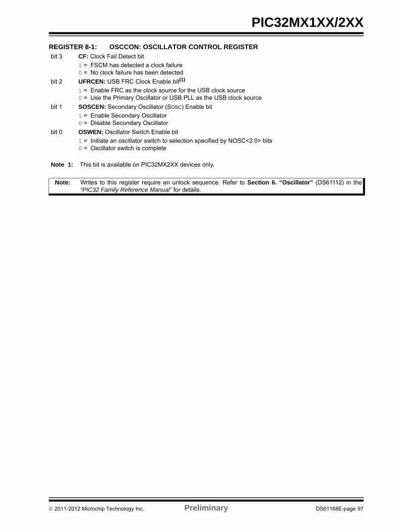
PIC32MX1XX/2XX
bit 3 CF: Clock Fail Detect bit
1 = FSCM has detected a clock failure0 = No clock failure has been detected
bit 2 UFRCEN: USB FRC Clock Enable bit(1)
1 = Enable FRC as the clock source for the USB clock source0 = Use the Primary Oscillator or USB PLL as the USB clock source
bit 1 SOSCEN: Secondary Oscillator (SOSC) Enable bit
1 = Enable Secondary Oscillator0 = Disable Secondary Oscillator
bit 0 OSWEN: Oscillator Switch Enable bit
1 = Initiate an oscillator switch to selection specified by NOSC<2:0> bits0 = Oscillator switch is complete
REGISTER 8-1: OSCCON: OSCILLATOR CONTROL REGISTER
Note 1: This bit is available on PIC32MX2XX devices only.
Note: Writes to this register require an unlock sequence. Refer to Section 6. “Oscillator” (DS61112) in the“PIC32 Family Reference Manual” for details.
2011-2012 Microchip Technology Inc. Preliminary DS61168E-page 97
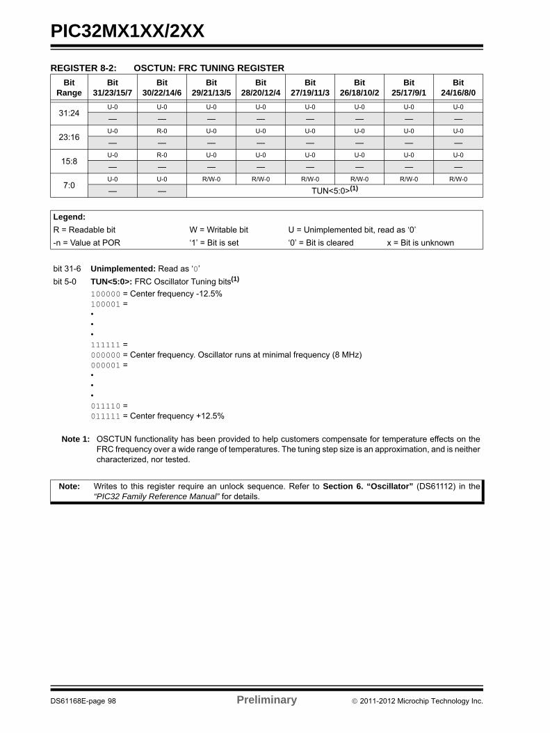
PIC32MX1XX/2XX
REGISTER 8-2: OSCTUN: FRC TUNING REGISTER
Bit Range
Bit31/23/15/7
Bit30/22/14/6
Bit29/21/13/5
Bit28/20/12/4
Bit27/19/11/3
Bit26/18/10/2
Bit25/17/9/1
Bit24/16/8/0
31:24U-0 U-0 U-0 U-0 U-0 U-0 U-0 U-0
— — — — — — — —
23:16U-0 R-0 U-0 U-0 U-0 U-0 U-0 U-0
— — — — — — — —
15:8U-0 R-0 U-0 U-0 U-0 U-0 U-0 U-0
— — — — — — — —
7:0U-0 U-0 R/W-0 R/W-0 R/W-0 R/W-0 R/W-0 R/W-0
— — TUN<5:0>(1)
Legend:
R = Readable bit W = Writable bit U = Unimplemented bit, read as ‘0’
-n = Value at POR ‘1’ = Bit is set ‘0’ = Bit is cleared x = Bit is unknown
bit 31-6 Unimplemented: Read as ‘0’
bit 5-0 TUN<5:0>: FRC Oscillator Tuning bits(1)
100000 = Center frequency -12.5%100001 = •••111111 =000000 = Center frequency. Oscillator runs at minimal frequency (8 MHz)000001 =•••011110 =011111 = Center frequency +12.5%
Note 1: OSCTUN functionality has been provided to help customers compensate for temperature effects on theFRC frequency over a wide range of temperatures. The tuning step size is an approximation, and is neithercharacterized, nor tested.
Note: Writes to this register require an unlock sequence. Refer to Section 6. “Oscillator” (DS61112) in the“PIC32 Family Reference Manual” for details.
DS61168E-page 98 Preliminary 2011-2012 Microchip Technology Inc.
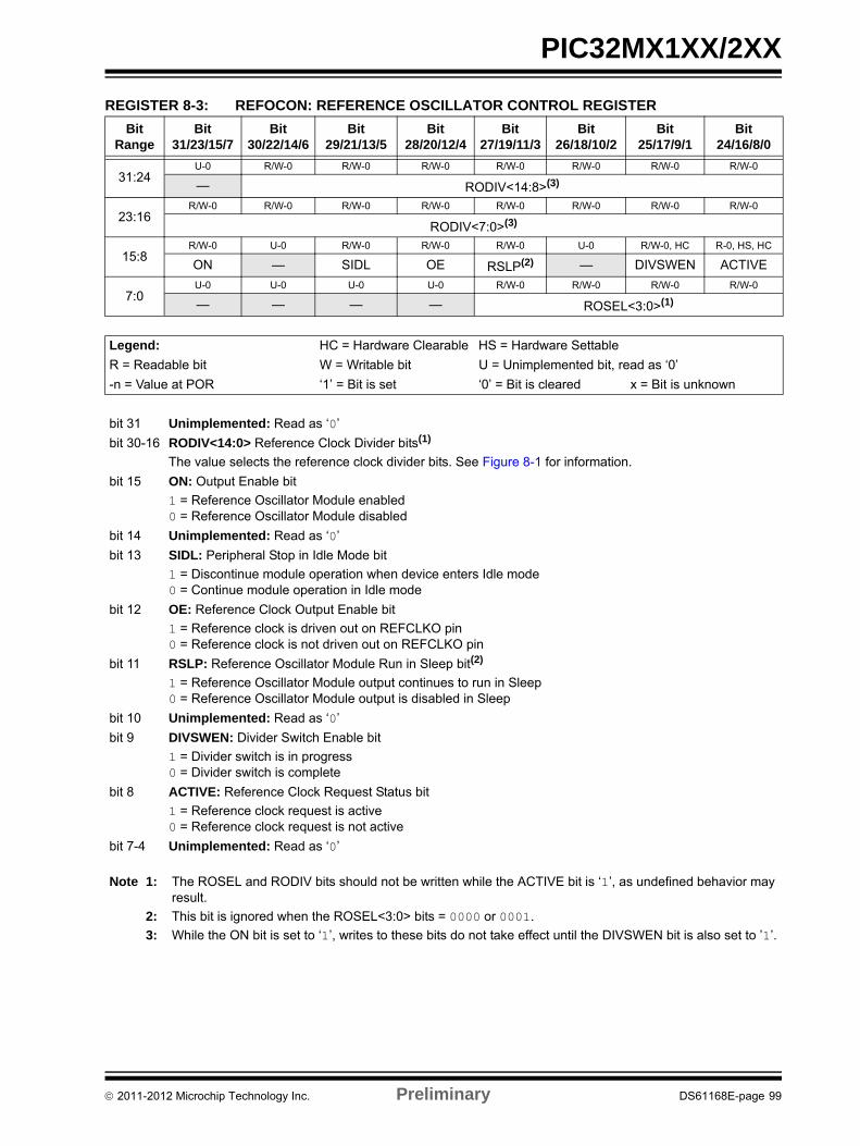
PIC32MX1XX/2XX
REGISTER 8-3: REFOCON: REFERENCE OSCILLATOR CONTROL REGISTER
Bit Range
Bit31/23/15/7
Bit30/22/14/6
Bit29/21/13/5
Bit28/20/12/4
Bit27/19/11/3
Bit26/18/10/2
Bit25/17/9/1
Bit24/16/8/0
31:24U-0 R/W-0 R/W-0 R/W-0 R/W-0 R/W-0 R/W-0 R/W-0
— RODIV<14:8>(3)
23:16R/W-0 R/W-0 R/W-0 R/W-0 R/W-0 R/W-0 R/W-0 R/W-0
RODIV<7:0>(3)
15:8R/W-0 U-0 R/W-0 R/W-0 R/W-0 U-0 R/W-0, HC R-0, HS, HC
ON — SIDL OE RSLP(2) — DIVSWEN ACTIVE
7:0U-0 U-0 U-0 U-0 R/W-0 R/W-0 R/W-0 R/W-0
— — — — ROSEL<3:0>(1)
Legend: HC = Hardware Clearable HS = Hardware Settable
R = Readable bit W = Writable bit U = Unimplemented bit, read as ‘0’
-n = Value at POR ‘1’ = Bit is set ‘0’ = Bit is cleared x = Bit is unknown
bit 31 Unimplemented: Read as ‘0’
bit 30-16 RODIV<14:0> Reference Clock Divider bits(1)
The value selects the reference clock divider bits. See Figure 8-1 for information.
bit 15 ON: Output Enable bit
1 = Reference Oscillator Module enabled0 = Reference Oscillator Module disabled
bit 14 Unimplemented: Read as ‘0’
bit 13 SIDL: Peripheral Stop in Idle Mode bit
1 = Discontinue module operation when device enters Idle mode0 = Continue module operation in Idle mode
bit 12 OE: Reference Clock Output Enable bit
1 = Reference clock is driven out on REFCLKO pin0 = Reference clock is not driven out on REFCLKO pin
bit 11 RSLP: Reference Oscillator Module Run in Sleep bit(2)
1 = Reference Oscillator Module output continues to run in Sleep0 = Reference Oscillator Module output is disabled in Sleep
bit 10 Unimplemented: Read as ‘0’
bit 9 DIVSWEN: Divider Switch Enable bit
1 = Divider switch is in progress0 = Divider switch is complete
bit 8 ACTIVE: Reference Clock Request Status bit
1 = Reference clock request is active0 = Reference clock request is not active
bit 7-4 Unimplemented: Read as ‘0’
Note 1: The ROSEL and RODIV bits should not be written while the ACTIVE bit is ‘1’, as undefined behavior may result.
2: This bit is ignored when the ROSEL<3:0> bits = 0000 or 0001.
3: While the ON bit is set to ‘1’, writes to these bits do not take effect until the DIVSWEN bit is also set to ’1’.
2011-2012 Microchip Technology Inc. Preliminary DS61168E-page 99
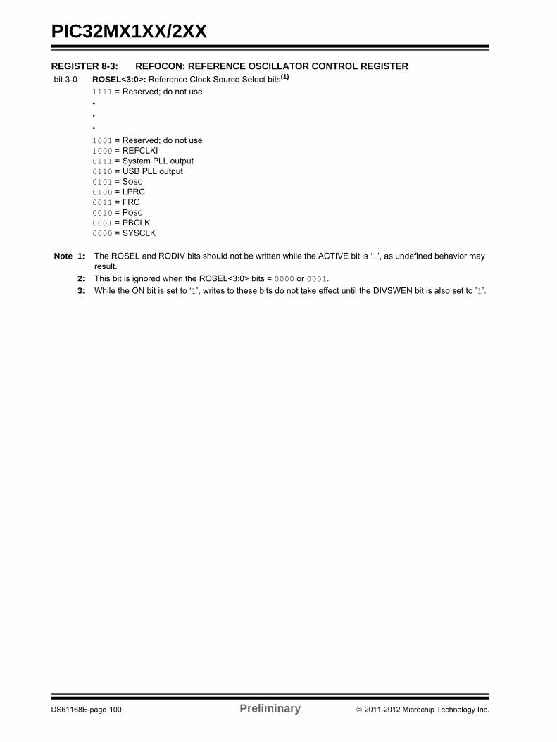
PIC32MX1XX/2XX
bit 3-0 ROSEL<3:0>: Reference Clock Source Select bits(1)
1111 = Reserved; do not use
•
•
•
1001 = Reserved; do not use1000 = REFCLKI0111 = System PLL output 0110 = USB PLL output0101 = SOSC
0100 = LPRC0011 = FRC0010 = POSC
0001 = PBCLK0000 = SYSCLK
REGISTER 8-3: REFOCON: REFERENCE OSCILLATOR CONTROL REGISTER
Note 1: The ROSEL and RODIV bits should not be written while the ACTIVE bit is ‘1’, as undefined behavior may result.
2: This bit is ignored when the ROSEL<3:0> bits = 0000 or 0001.
3: While the ON bit is set to ‘1’, writes to these bits do not take effect until the DIVSWEN bit is also set to ’1’.
DS61168E-page 100 Preliminary 2011-2012 Microchip Technology Inc.
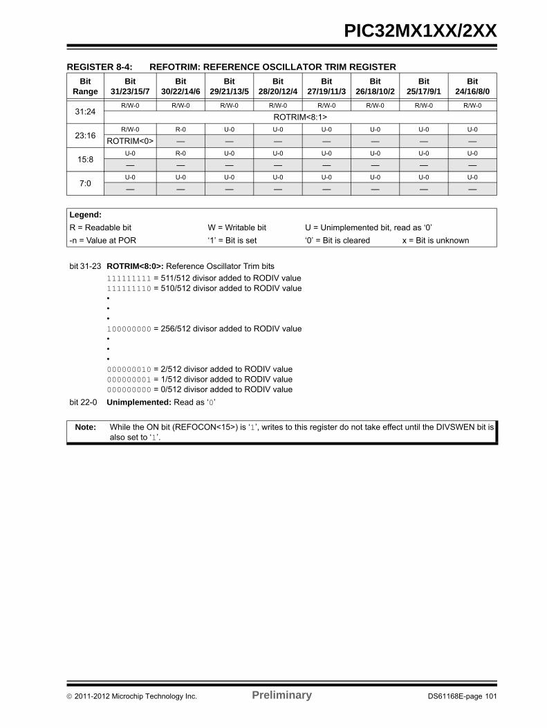
PIC32MX1XX/2XX
REGISTER 8-4: REFOTRIM: REFERENCE OSCILLATOR TRIM REGISTER
Bit Range
Bit31/23/15/7
Bit30/22/14/6
Bit29/21/13/5
Bit28/20/12/4
Bit27/19/11/3
Bit26/18/10/2
Bit25/17/9/1
Bit24/16/8/0
31:24R/W-0 R/W-0 R/W-0 R/W-0 R/W-0 R/W-0 R/W-0 R/W-0
ROTRIM<8:1>
23:16R/W-0 R-0 U-0 U-0 U-0 U-0 U-0 U-0
ROTRIM<0> — — — — — — —
15:8U-0 R-0 U-0 U-0 U-0 U-0 U-0 U-0
— — — — — — — —
7:0U-0 U-0 U-0 U-0 U-0 U-0 U-0 U-0
— — — — — — — —
Legend:
R = Readable bit W = Writable bit U = Unimplemented bit, read as ‘0’
-n = Value at POR ‘1’ = Bit is set ‘0’ = Bit is cleared x = Bit is unknown
bit 31-23 ROTRIM<8:0>: Reference Oscillator Trim bits
111111111 = 511/512 divisor added to RODIV value111111110 = 510/512 divisor added to RODIV value•••100000000 = 256/512 divisor added to RODIV value•••000000010 = 2/512 divisor added to RODIV value000000001 = 1/512 divisor added to RODIV value000000000 = 0/512 divisor added to RODIV value
bit 22-0 Unimplemented: Read as ‘0’
Note: While the ON bit (REFOCON<15>) is ‘1’, writes to this register do not take effect until the DIVSWEN bit isalso set to ‘1’.
2011-2012 Microchip Technology Inc. Preliminary DS61168E-page 101

PIC32MX1XX/2XX
NOTES:
DS61168E-page 102 Preliminary 2011-2012 Microchip Technology Inc.
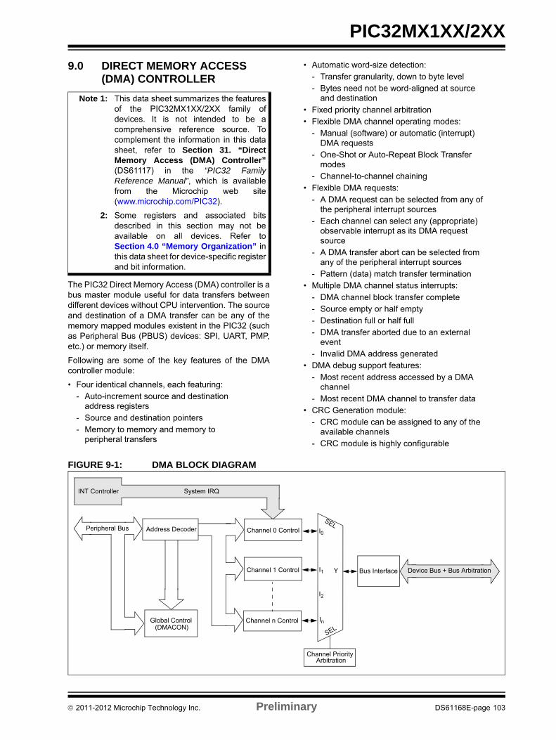
PIC32MX1XX/2XX
9.0 DIRECT MEMORY ACCESS (DMA) CONTROLLER
The PIC32 Direct Memory Access (DMA) controller is abus master module useful for data transfers betweendifferent devices without CPU intervention. The sourceand destination of a DMA transfer can be any of thememory mapped modules existent in the PIC32 (suchas Peripheral Bus (PBUS) devices: SPI, UART, PMP,etc.) or memory itself.
Following are some of the key features of the DMAcontroller module:
• Four identical channels, each featuring:- Auto-increment source and destination
address registers- Source and destination pointers- Memory to memory and memory to
peripheral transfers
• Automatic word-size detection:- Transfer granularity, down to byte level- Bytes need not be word-aligned at source
and destination• Fixed priority channel arbitration• Flexible DMA channel operating modes:
- Manual (software) or automatic (interrupt) DMA requests
- One-Shot or Auto-Repeat Block Transfer modes
- Channel-to-channel chaining• Flexible DMA requests:
- A DMA request can be selected from any of the peripheral interrupt sources
- Each channel can select any (appropriate) observable interrupt as its DMA request source
- A DMA transfer abort can be selected from any of the peripheral interrupt sources
- Pattern (data) match transfer termination• Multiple DMA channel status interrupts:
- DMA channel block transfer complete- Source empty or half empty- Destination full or half full- DMA transfer aborted due to an external
event- Invalid DMA address generated
• DMA debug support features:- Most recent address accessed by a DMA
channel- Most recent DMA channel to transfer data
• CRC Generation module:- CRC module can be assigned to any of the
available channels- CRC module is highly configurable
FIGURE 9-1: DMA BLOCK DIAGRAM
Note 1: This data sheet summarizes the featuresof the PIC32MX1XX/2XX family ofdevices. It is not intended to be acomprehensive reference source. Tocomplement the information in this datasheet, refer to Section 31. “DirectMemory Access (DMA) Controller”(DS61117) in the “PIC32 FamilyReference Manual”, which is availablefrom the Microchip web site(www.microchip.com/PIC32).
2: Some registers and associated bitsdescribed in this section may not beavailable on all devices. Refer toSection 4.0 “Memory Organization” inthis data sheet for device-specific registerand bit information.
Address Decoder Channel 0 Control
Channel 1 Control
Channel n ControlGlobal Control(DMACON)
Bus Interface
Channel PriorityArbitration
SEL
SEL
Y
I0
I1
I2
In
System IRQINT Controller
Device Bus + Bus Arbitration
Peripheral Bus
2011-2012 Microchip Technology Inc. Preliminary DS61168E-page 103
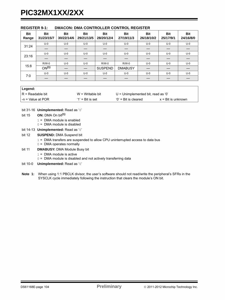
PIC32MX1XX/2XX
REGISTER 9-1: DMACON: DMA CONTROLLER CONTROL REGISTER
Bit Range
Bit31/23/15/7
Bit30/22/14/6
Bit29/21/13/5
Bit28/20/12/4
Bit27/19/11/3
Bit26/18/10/2
Bit25/17/9/1
Bit24/16/8/0
31:24U-0 U-0 U-0 U-0 U-0 U-0 U-0 U-0
— — — — — — — —
23:16U-0 U-0 U-0 U-0 U-0 U-0 U-0 U-0
— — — — — — — —
15:8R/W-0 U-0 U-0 R/W-0 R/W-0 U-0 U-0 U-0
ON(1) — — SUSPEND DMABUSY — — —
7:0U-0 U-0 U-0 U-0 U-0 U-0 U-0 U-0
— — — — — — — —
Legend:
R = Readable bit W = Writable bit U = Unimplemented bit, read as ‘0’
-n = Value at POR ‘1’ = Bit is set ‘0’ = Bit is cleared x = Bit is unknown
bit 31-16 Unimplemented: Read as ‘0’
bit 15 ON: DMA On bit(1)
1 = DMA module is enabled0 = DMA module is disabled
bit 14-13 Unimplemented: Read as ‘0’
bit 12 SUSPEND: DMA Suspend bit
1 = DMA transfers are suspended to allow CPU uninterrupted access to data bus0 = DMA operates normally
bit 11 DMABUSY: DMA Module Busy bit
1 = DMA module is active0 = DMA module is disabled and not actively transferring data
bit 10-0 Unimplemented: Read as ‘0’
Note 1: When using 1:1 PBCLK divisor, the user’s software should not read/write the peripheral’s SFRs in the SYSCLK cycle immediately following the instruction that clears the module’s ON bit.
DS61168E-page 104 Preliminary 2011-2012 Microchip Technology Inc.
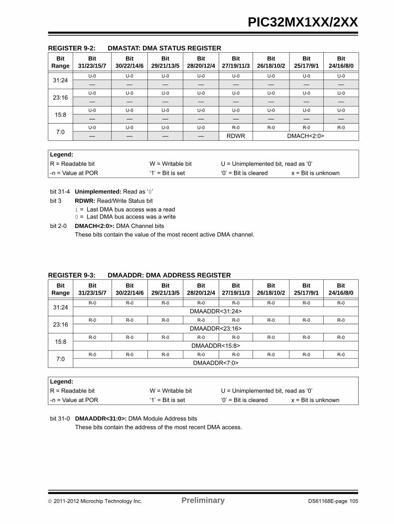
PIC32MX1XX/2XX
REGISTER 9-2: DMASTAT: DMA STATUS REGISTER
Bit Range
Bit31/23/15/7
Bit30/22/14/6
Bit29/21/13/5
Bit28/20/12/4
Bit27/19/11/3
Bit26/18/10/2
Bit25/17/9/1
Bit24/16/8/0
31:24U-0 U-0 U-0 U-0 U-0 U-0 U-0 U-0
— — — — — — — —
23:16U-0 U-0 U-0 U-0 U-0 U-0 U-0 U-0
— — — — — — — —
15:8U-0 U-0 U-0 U-0 U-0 U-0 U-0 U-0
— — — — — — — —
7:0U-0 U-0 U-0 U-0 R-0 R-0 R-0 R-0
— — — — RDWR DMACH<2:0>
Legend:
R = Readable bit W = Writable bit U = Unimplemented bit, read as ‘0’
-n = Value at POR ‘1’ = Bit is set ‘0’ = Bit is cleared x = Bit is unknown
bit 31-4 Unimplemented: Read as ‘0’
bit 3 RDWR: Read/Write Status bit
1 = Last DMA bus access was a read0 = Last DMA bus access was a write
bit 2-0 DMACH<2:0>: DMA Channel bits
These bits contain the value of the most recent active DMA channel.
REGISTER 9-3: DMAADDR: DMA ADDRESS REGISTER
Bit Range
Bit31/23/15/7
Bit30/22/14/6
Bit29/21/13/5
Bit28/20/12/4
Bit27/19/11/3
Bit26/18/10/2
Bit25/17/9/1
Bit24/16/8/0
31:24R-0 R-0 R-0 R-0 R-0 R-0 R-0 R-0
DMAADDR<31:24>
23:16R-0 R-0 R-0 R-0 R-0 R-0 R-0 R-0
DMAADDR<23:16>
15:8R-0 R-0 R-0 R-0 R-0 R-0 R-0 R-0
DMAADDR<15:8>
7:0R-0 R-0 R-0 R-0 R-0 R-0 R-0 R-0
DMAADDR<7:0>
Legend:
R = Readable bit W = Writable bit U = Unimplemented bit, read as ‘0’
-n = Value at POR ‘1’ = Bit is set ‘0’ = Bit is cleared x = Bit is unknown
bit 31-0 DMAADDR<31:0>: DMA Module Address bits
These bits contain the address of the most recent DMA access.
2011-2012 Microchip Technology Inc. Preliminary DS61168E-page 105
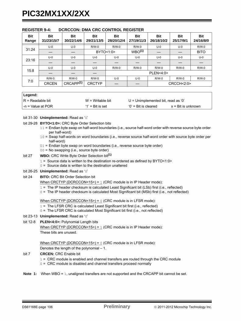
PIC32MX1XX/2XX
REGISTER 9-4: DCRCCON: DMA CRC CONTROL REGISTER
Bit Range
Bit31/23/15/7
Bit30/22/14/6
Bit29/21/13/5
Bit28/20/12/4
Bit27/19/11/3
Bit26/18/10/2
Bit25/17/9/1
Bit24/16/8/0
31:24U-0 U-0 R/W-0 R/W-0 R/W-0 U-0 U-0 R/W-0
— — BYTO<1:0> WBO(1) — — BITO
23:16U-0 U-0 U-0 U-0 U-0 U-0 U-0 U-0
— — — — — — — —
15:8U-0 U-0 U-0 R/W-0 R/W-0 R/W-0 R/W-0 R/W-0
— — — PLEN<4:0>
7:0R/W-0 R/W-0 R/W-0 U-0 U-0 R/W-0 R/W-0 R/W-0
CRCEN CRCAPP(1) CRCTYP — — CRCCH<2:0>
Legend:
R = Readable bit W = Writable bit U = Unimplemented bit, read as ‘0’
-n = Value at POR ‘1’ = Bit is set ‘0’ = Bit is cleared x = Bit is unknown
bit 31-30 Unimplemented: Read as ‘0’
bit 29-28 BYTO<1:0>: CRC Byte Order Selection bits11 = Endian byte swap on half-word boundaries (i.e., source half-word order with reverse source byte order
per half-word)10 = Swap half-words on word boundaries (i.e., reverse source half-word order with source byte order per
half-word)01 = Endian byte swap on word boundaries (i.e., reverse source byte order)00 = No swapping (i.e., source byte order)
bit 27 WBO: CRC Write Byte Order Selection bit(1)
1 = Source data is written to the destination re-ordered as defined by BYTO<1:0>0 = Source data is written to the destination unaltered
bit 26-25 Unimplemented: Read as ‘0’
bit 24 BITO: CRC Bit Order Selection bit
When CRCTYP (DCRCCON<15>) = 1 (CRC module is in IP Header mode):
1 = The IP header checksum is calculated Least Significant bit (LSb) first (i.e., reflected)0 = The IP header checksum is calculated Most Significant bit (MSb) first (i.e., not reflected)
When CRCTYP (DCRCCON<15>) = 0 (CRC module is in LFSR mode):
1 = The LFSR CRC is calculated Least Significant bit first (i.e., reflected)0 = The LFSR CRC is calculated Most Significant bit first (i.e., not reflected)
bit 23-13 Unimplemented: Read as ‘0’
bit 12-8 PLEN<4:0>: Polynomial Length bits
When CRCTYP (DCRCCON<15>) = 1 (CRC module is in IP Header mode):
These bits are unused.
When CRCTYP (DCRCCON<15>) = 0 (CRC module is in LFSR mode):
Denotes the length of the polynomial – 1.
bit 7 CRCEN: CRC Enable bit
1 = CRC module is enabled and channel transfers are routed through the CRC module0 = CRC module is disabled and channel transfers proceed normally
Note 1: When WBO = 1, unaligned transfers are not supported and the CRCAPP bit cannot be set.
DS61168E-page 106 Preliminary 2011-2012 Microchip Technology Inc.
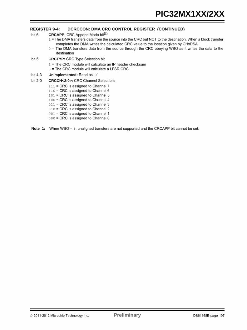
PIC32MX1XX/2XX
bit 6 CRCAPP: CRC Append Mode bit(1)
1 = The DMA transfers data from the source into the CRC but NOT to the destination. When a block transfercompletes the DMA writes the calculated CRC value to the location given by CHxDSA
0 = The DMA transfers data from the source through the CRC obeying WBO as it writes the data to thedestination
bit 5 CRCTYP: CRC Type Selection bit
1 = The CRC module will calculate an IP header checksum0 = The CRC module will calculate a LFSR CRC
bit 4-3 Unimplemented: Read as ‘0’
bit 2-0 CRCCH<2:0>: CRC Channel Select bits
111 = CRC is assigned to Channel 7110 = CRC is assigned to Channel 6101 = CRC is assigned to Channel 5100 = CRC is assigned to Channel 4011 = CRC is assigned to Channel 3010 = CRC is assigned to Channel 2001 = CRC is assigned to Channel 1000 = CRC is assigned to Channel 0
REGISTER 9-4: DCRCCON: DMA CRC CONTROL REGISTER (CONTINUED)
Note 1: When WBO = 1, unaligned transfers are not supported and the CRCAPP bit cannot be set.
2011-2012 Microchip Technology Inc. Preliminary DS61168E-page 107
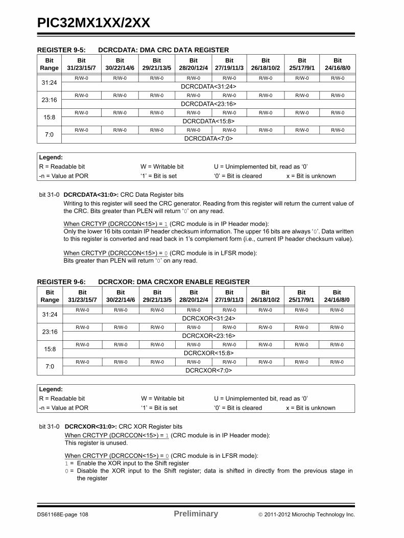
PIC32MX1XX/2XX
REGISTER 9-5: DCRCDATA: DMA CRC DATA REGISTER
Bit Range
Bit31/23/15/7
Bit30/22/14/6
Bit29/21/13/5
Bit28/20/12/4
Bit27/19/11/3
Bit26/18/10/2
Bit25/17/9/1
Bit24/16/8/0
31:24R/W-0 R/W-0 R/W-0 R/W-0 R/W-0 R/W-0 R/W-0 R/W-0
DCRCDATA<31:24>
23:16R/W-0 R/W-0 R/W-0 R/W-0 R/W-0 R/W-0 R/W-0 R/W-0
DCRCDATA<23:16>
15:8R/W-0 R/W-0 R/W-0 R/W-0 R/W-0 R/W-0 R/W-0 R/W-0
DCRCDATA<15:8>
7:0R/W-0 R/W-0 R/W-0 R/W-0 R/W-0 R/W-0 R/W-0 R/W-0
DCRCDATA<7:0>
Legend:
R = Readable bit W = Writable bit U = Unimplemented bit, read as ‘0’
-n = Value at POR ‘1’ = Bit is set ‘0’ = Bit is cleared x = Bit is unknown
bit 31-0 DCRCDATA<31:0>: CRC Data Register bits
Writing to this register will seed the CRC generator. Reading from this register will return the current value ofthe CRC. Bits greater than PLEN will return ‘0’ on any read.
When CRCTYP (DCRCCON<15>) = 1 (CRC module is in IP Header mode):Only the lower 16 bits contain IP header checksum information. The upper 16 bits are always ‘0’. Data writtento this register is converted and read back in 1’s complement form (i.e., current IP header checksum value).
When CRCTYP (DCRCCON<15>) = 0 (CRC module is in LFSR mode):Bits greater than PLEN will return ‘0’ on any read.
REGISTER 9-6: DCRCXOR: DMA CRCXOR ENABLE REGISTER
Bit Range
Bit31/23/15/7
Bit30/22/14/6
Bit29/21/13/5
Bit28/20/12/4
Bit27/19/11/3
Bit26/18/10/2
Bit25/17/9/1
Bit24/16/8/0
31:24R/W-0 R/W-0 R/W-0 R/W-0 R/W-0 R/W-0 R/W-0 R/W-0
DCRCXOR<31:24>
23:16R/W-0 R/W-0 R/W-0 R/W-0 R/W-0 R/W-0 R/W-0 R/W-0
DCRCXOR<23:16>
15:8R/W-0 R/W-0 R/W-0 R/W-0 R/W-0 R/W-0 R/W-0 R/W-0
DCRCXOR<15:8>
7:0R/W-0 R/W-0 R/W-0 R/W-0 R/W-0 R/W-0 R/W-0 R/W-0
DCRCXOR<7:0>
Legend:
R = Readable bit W = Writable bit U = Unimplemented bit, read as ‘0’
-n = Value at POR ‘1’ = Bit is set ‘0’ = Bit is cleared x = Bit is unknown
bit 31-0 DCRCXOR<31:0>: CRC XOR Register bits
When CRCTYP (DCRCCON<15>) = 1 (CRC module is in IP Header mode):This register is unused.
When CRCTYP (DCRCCON<15>) = 0 (CRC module is in LFSR mode):1 = Enable the XOR input to the Shift register0 = Disable the XOR input to the Shift register; data is shifted in directly from the previous stage in
the register
DS61168E-page 108 Preliminary 2011-2012 Microchip Technology Inc.
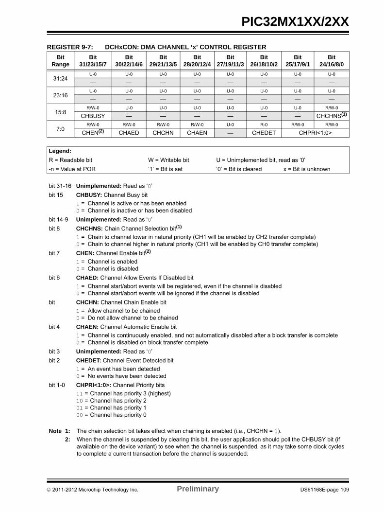
PIC32MX1XX/2XX
REGISTER 9-7: DCHxCON: DMA CHANNEL ‘x’ CONTROL REGISTER
Bit Range
Bit31/23/15/7
Bit30/22/14/6
Bit29/21/13/5
Bit28/20/12/4
Bit27/19/11/3
Bit26/18/10/2
Bit25/17/9/1
Bit24/16/8/0
31:24U-0 U-0 U-0 U-0 U-0 U-0 U-0 U-0
— — — — — — — —
23:16U-0 U-0 U-0 U-0 U-0 U-0 U-0 U-0
— — — — — — — —
15:8R/W-0 U-0 U-0 U-0 U-0 U-0 U-0 R/W-0
CHBUSY — — — — — — CHCHNS(1)
7:0R/W-0 R/W-0 R/W-0 R/W-0 U-0 R-0 R/W-0 R/W-0
CHEN(2) CHAED CHCHN CHAEN — CHEDET CHPRI<1:0>
Legend:
R = Readable bit W = Writable bit U = Unimplemented bit, read as ‘0’
-n = Value at POR ‘1’ = Bit is set ‘0’ = Bit is cleared x = Bit is unknown
bit 31-16 Unimplemented: Read as ‘0’
bit 15 CHBUSY: Channel Busy bit
1 = Channel is active or has been enabled0 = Channel is inactive or has been disabled
bit 14-9 Unimplemented: Read as ‘0’
bit 8 CHCHNS: Chain Channel Selection bit(1)
1 = Chain to channel lower in natural priority (CH1 will be enabled by CH2 transfer complete)0 = Chain to channel higher in natural priority (CH1 will be enabled by CH0 transfer complete)
bit 7 CHEN: Channel Enable bit(2)
1 = Channel is enabled0 = Channel is disabled
bit 6 CHAED: Channel Allow Events If Disabled bit
1 = Channel start/abort events will be registered, even if the channel is disabled0 = Channel start/abort events will be ignored if the channel is disabled
bit CHCHN: Channel Chain Enable bit
1 = Allow channel to be chained0 = Do not allow channel to be chained
bit 4 CHAEN: Channel Automatic Enable bit
1 = Channel is continuously enabled, and not automatically disabled after a block transfer is complete0 = Channel is disabled on block transfer complete
bit 3 Unimplemented: Read as ‘0’
bit 2 CHEDET: Channel Event Detected bit
1 = An event has been detected0 = No events have been detected
bit 1-0 CHPRI<1:0>: Channel Priority bits
11 = Channel has priority 3 (highest)10 = Channel has priority 201 = Channel has priority 100 = Channel has priority 0
Note 1: The chain selection bit takes effect when chaining is enabled (i.e., CHCHN = 1).
2: When the channel is suspended by clearing this bit, the user application should poll the CHBUSY bit (if available on the device variant) to see when the channel is suspended, as it may take some clock cycles to complete a current transaction before the channel is suspended.
2011-2012 Microchip Technology Inc. Preliminary DS61168E-page 109
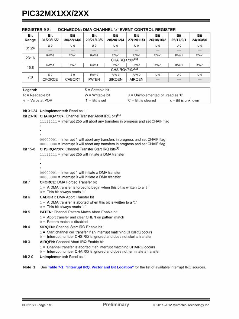
PIC32MX1XX/2XX
REGISTER 9-8: DCHxECON: DMA CHANNEL ‘x’ EVENT CONTROL REGISTER
Bit Range
Bit31/23/15/7
Bit30/22/14/6
Bit29/21/13/5
Bit28/20/12/4
Bit27/19/11/3
Bit26/18/10/2
Bit25/17/9/1
Bit24/16/8/0
31:24U-0 U-0 U-0 U-0 U-0 U-0 U-0 U-0
— — — — — — — —
23:16R/W-1 R/W-1 R/W-1 R/W-1 R/W-1 R/W-1 R/W-1 R/W-1
CHAIRQ<7:0>(1)
15:8R/W-1 R/W-1 R/W-1 R/W-1 R/W-1 R/W-1 R/W-1 R/W-1
CHSIRQ<7:0>(1)
7:0S-0 S-0 R/W-0 R/W-0 R/W-0 U-0 U-0 U-0
CFORCE CABORT PATEN SIRQEN AIRQEN — — —
Legend: S = Settable bit
R = Readable bit W = Writable bit U = Unimplemented bit, read as ‘0’
-n = Value at POR ‘1’ = Bit is set ‘0’ = Bit is cleared x = Bit is unknown
bit 31-24 Unimplemented: Read as ‘0’
bit 23-16 CHAIRQ<7:0>: Channel Transfer Abort IRQ bits(1)
11111111 = Interrupt 255 will abort any transfers in progress and set CHAIF flag•••
00000001 = Interrupt 1 will abort any transfers in progress and set CHAIF flag00000000 = Interrupt 0 will abort any transfers in progress and set CHAIF flag
bit 15-8 CHSIRQ<7:0>: Channel Transfer Start IRQ bits(1)
11111111 = Interrupt 255 will initiate a DMA transfer•••
00000001 = Interrupt 1 will initiate a DMA transfer00000000 = Interrupt 0 will initiate a DMA transfer
bit 7 CFORCE: DMA Forced Transfer bit
1 = A DMA transfer is forced to begin when this bit is written to a ‘1’0 = This bit always reads ‘0’
bit 6 CABORT: DMA Abort Transfer bit
1 = A DMA transfer is aborted when this bit is written to a ‘1’0 = This bit always reads ‘0’
bit 5 PATEN: Channel Pattern Match Abort Enable bit
1 = Abort transfer and clear CHEN on pattern match0 = Pattern match is disabled
bit 4 SIRQEN: Channel Start IRQ Enable bit
1 = Start channel cell transfer if an interrupt matching CHSIRQ occurs0 = Interrupt number CHSIRQ is ignored and does not start a transfer
bit 3 AIRQEN: Channel Abort IRQ Enable bit
1 = Channel transfer is aborted if an interrupt matching CHAIRQ occurs0 = Interrupt number CHAIRQ is ignored and does not terminate a transfer
bit 2-0 Unimplemented: Read as ‘0’
Note 1: See Table 7-1: “Interrupt IRQ, Vector and Bit Location” for the list of available interrupt IRQ sources.
DS61168E-page 110 Preliminary 2011-2012 Microchip Technology Inc.
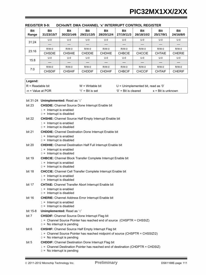
PIC32MX1XX/2XX
REGISTER 9-9: DCHxINT: DMA CHANNEL ‘x’ INTERRUPT CONTROL REGISTER
Bit Range
Bit31/23/15/7
Bit30/22/14/6
Bit29/21/13/5
Bit28/20/12/4
Bit27/19/11/3
Bit26/18/10/2
Bit25/17/9/1
Bit24/16/8/0
31:24U-0 U-0 U-0 U-0 U-0 U-0 U-0 U-0
— — — — — — — —
23:16R/W-0 R/W-0 R/W-0 R/W-0 R/W-0 R/W-0 R/W-0 R/W-0
CHSDIE CHSHIE CHDDIE CHDHIE CHBCIE CHCCIE CHTAIE CHERIE
15:8U-0 U-0 U-0 U-0 U-0 U-0 U-0 U-0
— — — — — — — —
7:0R/W-0 R/W-0 R/W-0 R/W-0 R/W-0 R/W-0 R/W-0 R/W-0
CHSDIF CHSHIF CHDDIF CHDHIF CHBCIF CHCCIF CHTAIF CHERIF
Legend:
R = Readable bit W = Writable bit U = Unimplemented bit, read as ‘0’
-n = Value at POR ‘1’ = Bit is set ‘0’ = Bit is cleared x = Bit is unknown
bit 31-24 Unimplemented: Read as ‘0’
bit 23 CHSDIE: Channel Source Done Interrupt Enable bit
1 = Interrupt is enabled0 = Interrupt is disabled
bit 22 CHSHIE: Channel Source Half Empty Interrupt Enable bit
1 = Interrupt is enabled0 = Interrupt is disabled
bit 21 CHDDIE: Channel Destination Done Interrupt Enable bit
1 = Interrupt is enabled0 = Interrupt is disabled
bit 20 CHDHIE: Channel Destination Half Full Interrupt Enable bit
1 = Interrupt is enabled0 = Interrupt is disabled
bit 19 CHBCIE: Channel Block Transfer Complete Interrupt Enable bit
1 = Interrupt is enabled0 = Interrupt is disabled
bit 18 CHCCIE: Channel Cell Transfer Complete Interrupt Enable bit
1 = Interrupt is enabled0 = Interrupt is disabled
bit 17 CHTAIE: Channel Transfer Abort Interrupt Enable bit
1 = Interrupt is enabled0 = Interrupt is disabled
bit 16 CHERIE: Channel Address Error Interrupt Enable bit
1 = Interrupt is enabled0 = Interrupt is disabled
bit 15-8 Unimplemented: Read as ‘0’
bit 7 CHSDIF: Channel Source Done Interrupt Flag bit
1 = Channel Source Pointer has reached end of source (CHSPTR = CHSSIZ)0 = No interrupt is pending
bit 6 CHSHIF: Channel Source Half Empty Interrupt Flag bit
1 = Channel Source Pointer has reached midpoint of source (CHSPTR = CHSSIZ/2) 0 = No interrupt is pending
bit 5 CHDDIF: Channel Destination Done Interrupt Flag bit
1 = Channel Destination Pointer has reached end of destination (CHDPTR = CHDSIZ) 0 = No interrupt is pending
2011-2012 Microchip Technology Inc. Preliminary DS61168E-page 111
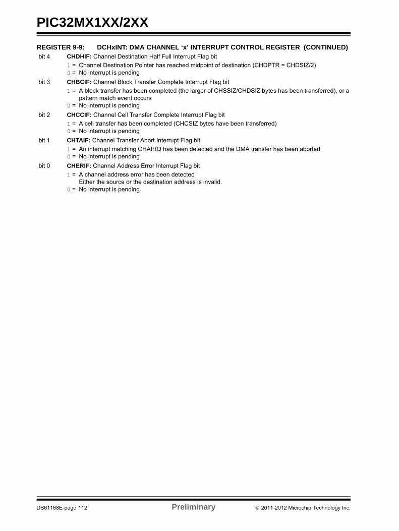
PIC32MX1XX/2XX
bit 4 CHDHIF: Channel Destination Half Full Interrupt Flag bit
1 = Channel Destination Pointer has reached midpoint of destination (CHDPTR = CHDSIZ/2) 0 = No interrupt is pending
bit 3 CHBCIF: Channel Block Transfer Complete Interrupt Flag bit
1 = A block transfer has been completed (the larger of CHSSIZ/CHDSIZ bytes has been transferred), or apattern match event occurs
0 = No interrupt is pending
bit 2 CHCCIF: Channel Cell Transfer Complete Interrupt Flag bit
1 = A cell transfer has been completed (CHCSIZ bytes have been transferred) 0 = No interrupt is pending
bit 1 CHTAIF: Channel Transfer Abort Interrupt Flag bit
1 = An interrupt matching CHAIRQ has been detected and the DMA transfer has been aborted 0 = No interrupt is pending
bit 0 CHERIF: Channel Address Error Interrupt Flag bit
1 = A channel address error has been detected Either the source or the destination address is invalid.
0 = No interrupt is pending
REGISTER 9-9: DCHxINT: DMA CHANNEL ‘x’ INTERRUPT CONTROL REGISTER (CONTINUED)
DS61168E-page 112 Preliminary 2011-2012 Microchip Technology Inc.
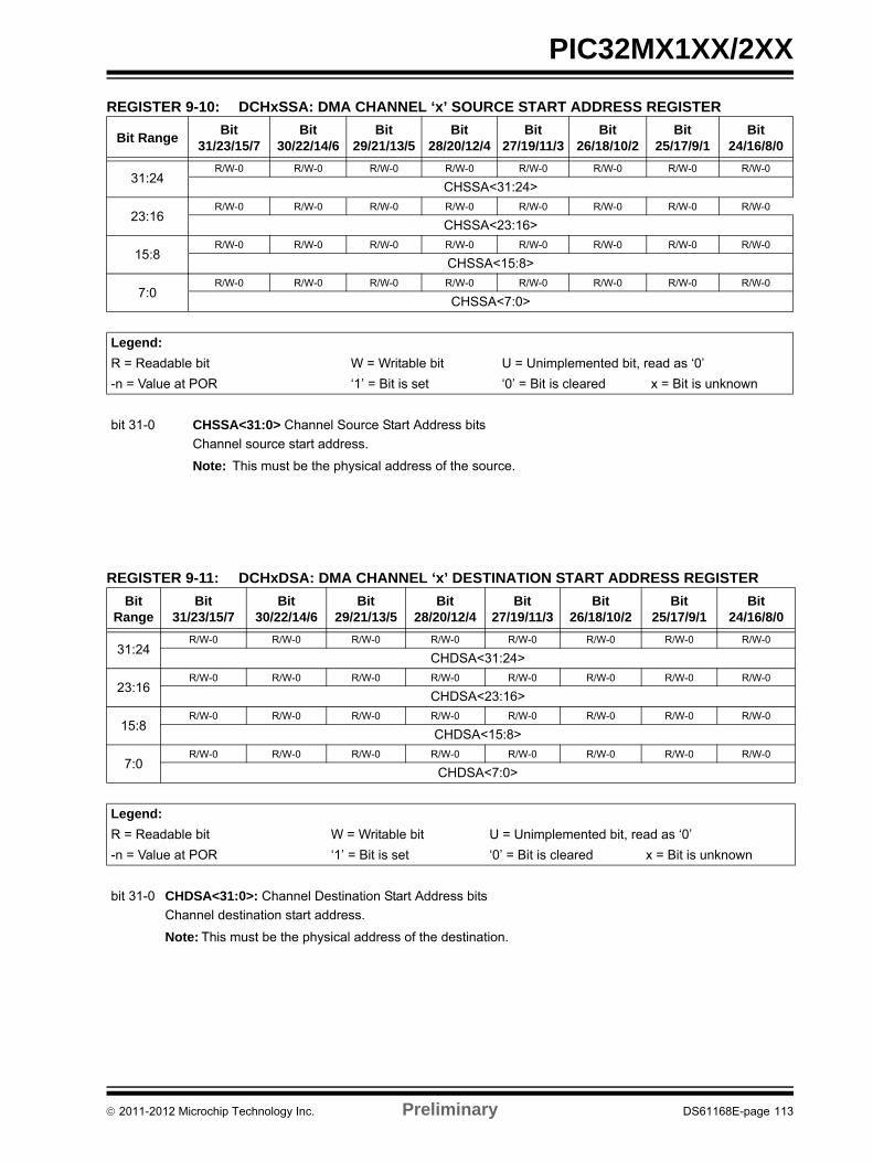
PIC32MX1XX/2XX
REGISTER 9-10: DCHxSSA: DMA CHANNEL ‘x’ SOURCE START ADDRESS REGISTER
Bit RangeBit
31/23/15/7Bit
30/22/14/6Bit
29/21/13/5Bit
28/20/12/4Bit
27/19/11/3Bit
26/18/10/2Bit
25/17/9/1Bit
24/16/8/0
31:24R/W-0 R/W-0 R/W-0 R/W-0 R/W-0 R/W-0 R/W-0 R/W-0
CHSSA<31:24>
23:16R/W-0 R/W-0 R/W-0 R/W-0 R/W-0 R/W-0 R/W-0 R/W-0
CHSSA<23:16>
15:8R/W-0 R/W-0 R/W-0 R/W-0 R/W-0 R/W-0 R/W-0 R/W-0
CHSSA<15:8>
7:0R/W-0 R/W-0 R/W-0 R/W-0 R/W-0 R/W-0 R/W-0 R/W-0
CHSSA<7:0>
Legend:
R = Readable bit W = Writable bit U = Unimplemented bit, read as ‘0’
-n = Value at POR ‘1’ = Bit is set ‘0’ = Bit is cleared x = Bit is unknown
bit 31-0 CHSSA<31:0> Channel Source Start Address bits
Channel source start address.
Note: This must be the physical address of the source.
REGISTER 9-11: DCHxDSA: DMA CHANNEL ‘x’ DESTINATION START ADDRESS REGISTER
Bit Range
Bit31/23/15/7
Bit30/22/14/6
Bit29/21/13/5
Bit28/20/12/4
Bit27/19/11/3
Bit26/18/10/2
Bit25/17/9/1
Bit24/16/8/0
31:24R/W-0 R/W-0 R/W-0 R/W-0 R/W-0 R/W-0 R/W-0 R/W-0
CHDSA<31:24>
23:16R/W-0 R/W-0 R/W-0 R/W-0 R/W-0 R/W-0 R/W-0 R/W-0
CHDSA<23:16>
15:8R/W-0 R/W-0 R/W-0 R/W-0 R/W-0 R/W-0 R/W-0 R/W-0
CHDSA<15:8>
7:0R/W-0 R/W-0 R/W-0 R/W-0 R/W-0 R/W-0 R/W-0 R/W-0
CHDSA<7:0>
Legend:
R = Readable bit W = Writable bit U = Unimplemented bit, read as ‘0’
-n = Value at POR ‘1’ = Bit is set ‘0’ = Bit is cleared x = Bit is unknown
bit 31-0 CHDSA<31:0>: Channel Destination Start Address bits
Channel destination start address.
Note: This must be the physical address of the destination.
2011-2012 Microchip Technology Inc. Preliminary DS61168E-page 113
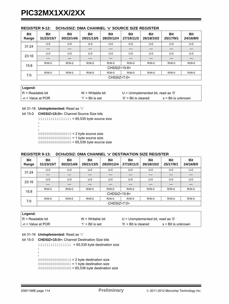
PIC32MX1XX/2XX
REGISTER 9-12: DCHxSSIZ: DMA CHANNEL ‘x’ SOURCE SIZE REGISTER
Bit Range
Bit31/23/15/7
Bit30/22/14/6
Bit29/21/13/5
Bit28/20/12/4
Bit27/19/11/3
Bit26/18/10/2
Bit25/17/9/1
Bit24/16/8/0
31:24U-0 U-0 U-0 U-0 U-0 U-0 U-0 U-0
— — — — — — — —
23:16U-0 U-0 U-0 U-0 U-0 U-0 U-0 U-0
— — — — — — — —
15:8R/W-0 R/W-0 R/W-0 R/W-0 R/W-0 R/W-0 R/W-0 R/W-0
CHSSIZ<15:8>
7:0R/W-0 R/W-0 R/W-0 R/W-0 R/W-0 R/W-0 R/W-0 R/W-0
CHSSIZ<7:0>
Legend:
R = Readable bit W = Writable bit U = Unimplemented bit, read as ‘0’
-n = Value at POR ‘1’ = Bit is set ‘0’ = Bit is cleared x = Bit is unknown
bit 31-16 Unimplemented: Read as ‘0’
bit 15-0 CHSSIZ<15:0>: Channel Source Size bits
1111111111111111 = 65,535 byte source size•••
0000000000000010 = 2 byte source size0000000000000001 = 1 byte source size0000000000000000 = 65,536 byte source size
REGISTER 9-13: DCHxDSIZ: DMA CHANNEL ‘x’ DESTINATION SIZE REGISTER
Bit Range
Bit31/23/15/7
Bit30/22/14/6
Bit29/21/13/5
Bit28/20/12/4
Bit27/19/11/3
Bit26/18/10/2
Bit25/17/9/1
Bit24/16/8/0
31:24U-0 U-0 U-0 U-0 U-0 U-0 U-0 U-0
— — — — — — — —
23:16U-0 U-0 U-0 U-0 U-0 U-0 U-0 U-0
— — — — — — — —
15:8R/W-0 R/W-0 R/W-0 R/W-0 R/W-0 R/W-0 R/W-0 R/W-0
CHDSIZ<15:8>
7:0R/W-0 R/W-0 R/W-0 R/W-0 R/W-0 R/W-0 R/W-0 R/W-0
CHDSIZ<7:0>
Legend:
R = Readable bit W = Writable bit U = Unimplemented bit, read as ‘0’
-n = Value at POR ‘1’ = Bit is set ‘0’ = Bit is cleared x = Bit is unknown
bit 31-16 Unimplemented: Read as ‘0’
bit 15-0 CHDSIZ<15:0>: Channel Destination Size bits
1111111111111111 = 65,535 byte destination size•••
0000000000000010 = 2 byte destination size0000000000000001 = 1 byte destination size0000000000000000 = 65,536 byte destination size
DS61168E-page 114 Preliminary 2011-2012 Microchip Technology Inc.
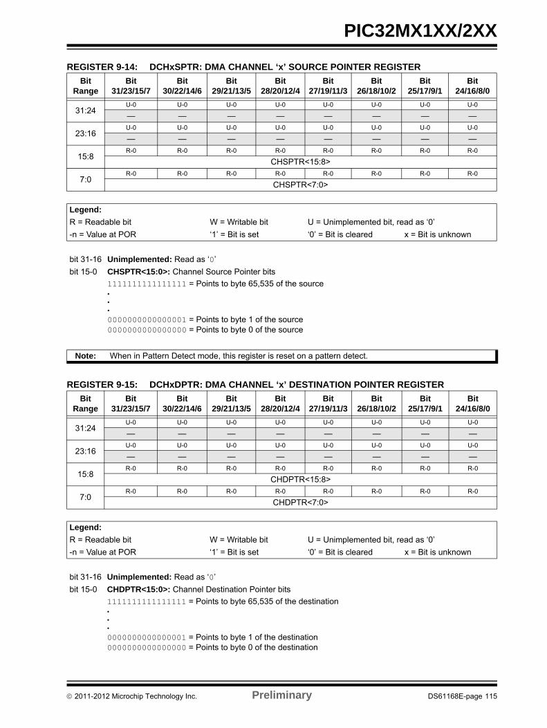
PIC32MX1XX/2XX
REGISTER 9-14: DCHxSPTR: DMA CHANNEL ‘x’ SOURCE POINTER REGISTER
Bit Range
Bit31/23/15/7
Bit30/22/14/6
Bit29/21/13/5
Bit28/20/12/4
Bit27/19/11/3
Bit26/18/10/2
Bit25/17/9/1
Bit24/16/8/0
31:24U-0 U-0 U-0 U-0 U-0 U-0 U-0 U-0
— — — — — — — —
23:16U-0 U-0 U-0 U-0 U-0 U-0 U-0 U-0
— — — — — — — —
15:8R-0 R-0 R-0 R-0 R-0 R-0 R-0 R-0
CHSPTR<15:8>
7:0R-0 R-0 R-0 R-0 R-0 R-0 R-0 R-0
CHSPTR<7:0>
Legend:
R = Readable bit W = Writable bit U = Unimplemented bit, read as ‘0’
-n = Value at POR ‘1’ = Bit is set ‘0’ = Bit is cleared x = Bit is unknown
bit 31-16 Unimplemented: Read as ‘0’
bit 15-0 CHSPTR<15:0>: Channel Source Pointer bits
1111111111111111 = Points to byte 65,535 of the source•••
0000000000000001 = Points to byte 1 of the source0000000000000000 = Points to byte 0 of the source
Note: When in Pattern Detect mode, this register is reset on a pattern detect.
REGISTER 9-15: DCHxDPTR: DMA CHANNEL ‘x’ DESTINATION POINTER REGISTER
Bit Range
Bit31/23/15/7
Bit30/22/14/6
Bit29/21/13/5
Bit28/20/12/4
Bit27/19/11/3
Bit26/18/10/2
Bit25/17/9/1
Bit24/16/8/0
31:24U-0 U-0 U-0 U-0 U-0 U-0 U-0 U-0
— — — — — — — —
23:16U-0 U-0 U-0 U-0 U-0 U-0 U-0 U-0
— — — — — — — —
15:8R-0 R-0 R-0 R-0 R-0 R-0 R-0 R-0
CHDPTR<15:8>
7:0R-0 R-0 R-0 R-0 R-0 R-0 R-0 R-0
CHDPTR<7:0>
Legend:
R = Readable bit W = Writable bit U = Unimplemented bit, read as ‘0’
-n = Value at POR ‘1’ = Bit is set ‘0’ = Bit is cleared x = Bit is unknown
bit 31-16 Unimplemented: Read as ‘0’
bit 15-0 CHDPTR<15:0>: Channel Destination Pointer bits
1111111111111111 = Points to byte 65,535 of the destination•••
0000000000000001 = Points to byte 1 of the destination0000000000000000 = Points to byte 0 of the destination
2011-2012 Microchip Technology Inc. Preliminary DS61168E-page 115
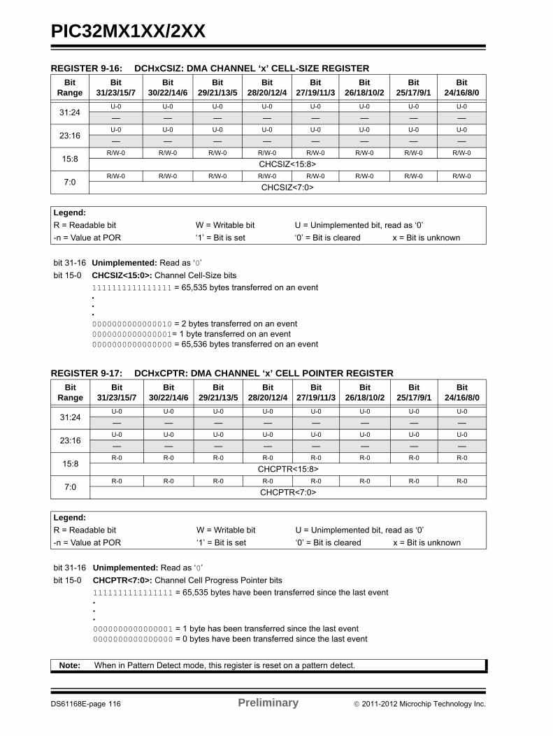
PIC32MX1XX/2XX
REGISTER 9-16: DCHxCSIZ: DMA CHANNEL ‘x’ CELL-SIZE REGISTER
Bit Range
Bit31/23/15/7
Bit30/22/14/6
Bit29/21/13/5
Bit28/20/12/4
Bit27/19/11/3
Bit26/18/10/2
Bit25/17/9/1
Bit24/16/8/0
31:24U-0 U-0 U-0 U-0 U-0 U-0 U-0 U-0
— — — — — — — —
23:16U-0 U-0 U-0 U-0 U-0 U-0 U-0 U-0
— — — — — — — —
15:8R/W-0 R/W-0 R/W-0 R/W-0 R/W-0 R/W-0 R/W-0 R/W-0
CHCSIZ<15:8>
7:0R/W-0 R/W-0 R/W-0 R/W-0 R/W-0 R/W-0 R/W-0 R/W-0
CHCSIZ<7:0>
Legend:
R = Readable bit W = Writable bit U = Unimplemented bit, read as ‘0’
-n = Value at POR ‘1’ = Bit is set ‘0’ = Bit is cleared x = Bit is unknown
bit 31-16 Unimplemented: Read as ‘0’
bit 15-0 CHCSIZ<15:0>: Channel Cell-Size bits
1111111111111111 = 65,535 bytes transferred on an event•••
0000000000000010 = 2 bytes transferred on an event0000000000000001= 1 byte transferred on an event0000000000000000 = 65,536 bytes transferred on an event
REGISTER 9-17: DCHxCPTR: DMA CHANNEL ‘x’ CELL POINTER REGISTER
Bit Range
Bit31/23/15/7
Bit30/22/14/6
Bit29/21/13/5
Bit28/20/12/4
Bit27/19/11/3
Bit26/18/10/2
Bit25/17/9/1
Bit24/16/8/0
31:24U-0 U-0 U-0 U-0 U-0 U-0 U-0 U-0
— — — — — — — —
23:16U-0 U-0 U-0 U-0 U-0 U-0 U-0 U-0
— — — — — — — —
15:8R-0 R-0 R-0 R-0 R-0 R-0 R-0 R-0
CHCPTR<15:8>
7:0R-0 R-0 R-0 R-0 R-0 R-0 R-0 R-0
CHCPTR<7:0>
Legend:
R = Readable bit W = Writable bit U = Unimplemented bit, read as ‘0’
-n = Value at POR ‘1’ = Bit is set ‘0’ = Bit is cleared x = Bit is unknown
bit 31-16 Unimplemented: Read as ‘0’
bit 15-0 CHCPTR<7:0>: Channel Cell Progress Pointer bits
1111111111111111 = 65,535 bytes have been transferred since the last event•••
0000000000000001 = 1 byte has been transferred since the last event0000000000000000 = 0 bytes have been transferred since the last event
Note: When in Pattern Detect mode, this register is reset on a pattern detect.
DS61168E-page 116 Preliminary 2011-2012 Microchip Technology Inc.
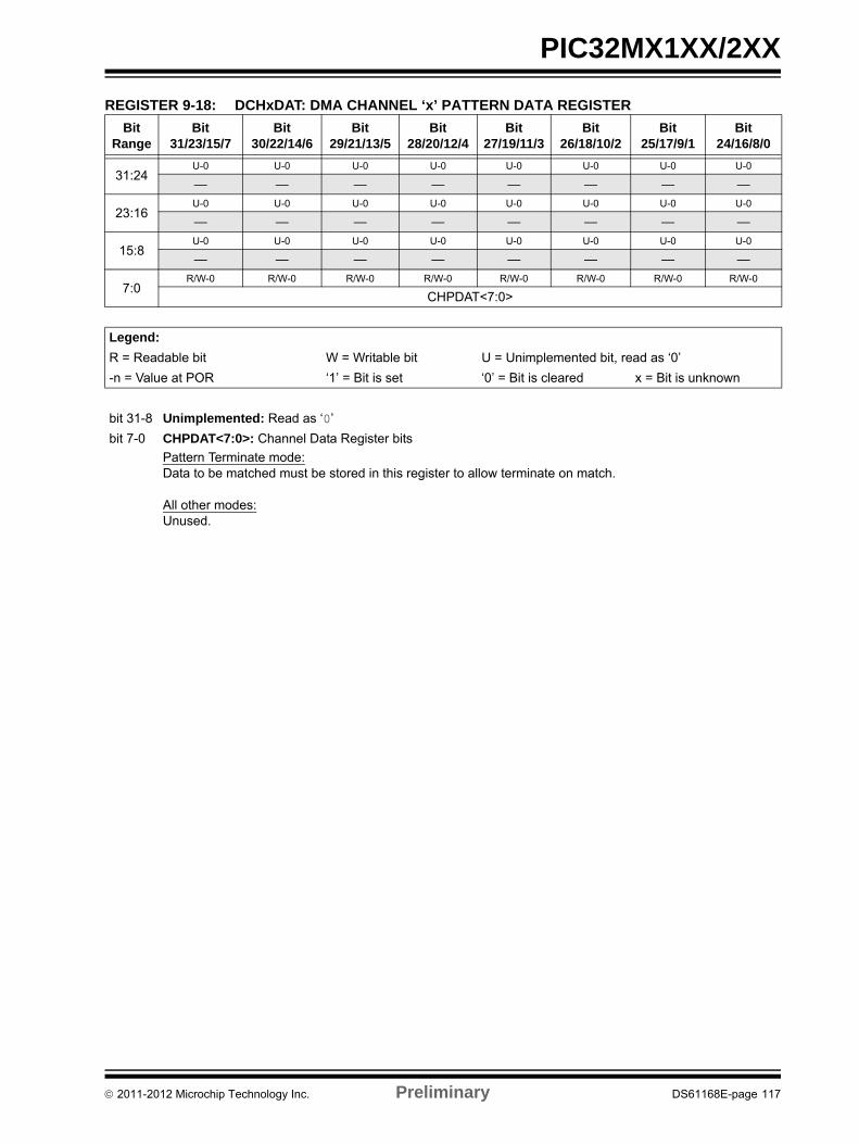
PIC32MX1XX/2XX
REGISTER 9-18: DCHxDAT: DMA CHANNEL ‘x’ PATTERN DATA REGISTER
Bit Range
Bit31/23/15/7
Bit30/22/14/6
Bit29/21/13/5
Bit28/20/12/4
Bit27/19/11/3
Bit26/18/10/2
Bit25/17/9/1
Bit24/16/8/0
31:24U-0 U-0 U-0 U-0 U-0 U-0 U-0 U-0
— — — — — — — —
23:16U-0 U-0 U-0 U-0 U-0 U-0 U-0 U-0
— — — — — — — —
15:8U-0 U-0 U-0 U-0 U-0 U-0 U-0 U-0
— — — — — — — —
7:0R/W-0 R/W-0 R/W-0 R/W-0 R/W-0 R/W-0 R/W-0 R/W-0
CHPDAT<7:0>
Legend:
R = Readable bit W = Writable bit U = Unimplemented bit, read as ‘0’
-n = Value at POR ‘1’ = Bit is set ‘0’ = Bit is cleared x = Bit is unknown
bit 31-8 Unimplemented: Read as ‘0’
bit 7-0 CHPDAT<7:0>: Channel Data Register bits
Pattern Terminate mode:Data to be matched must be stored in this register to allow terminate on match.
All other modes:Unused.
2011-2012 Microchip Technology Inc. Preliminary DS61168E-page 117

PIC32MX1XX/2XX
NOTES:
DS61168E-page 118 Preliminary 2011-2012 Microchip Technology Inc.
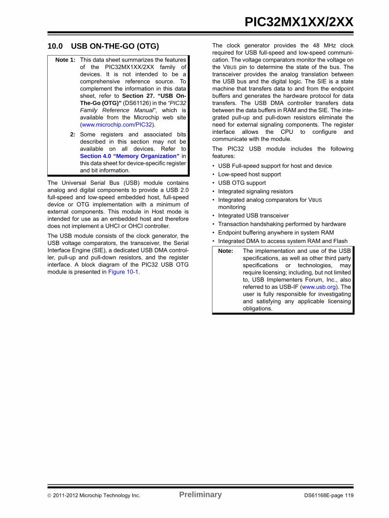
PIC32MX1XX/2XX
10.0 USB ON-THE-GO (OTG)
The Universal Serial Bus (USB) module containsanalog and digital components to provide a USB 2.0full-speed and low-speed embedded host, full-speeddevice or OTG implementation with a minimum ofexternal components. This module in Host mode isintended for use as an embedded host and thereforedoes not implement a UHCI or OHCI controller.
The USB module consists of the clock generator, theUSB voltage comparators, the transceiver, the SerialInterface Engine (SIE), a dedicated USB DMA control-ler, pull-up and pull-down resistors, and the registerinterface. A block diagram of the PIC32 USB OTGmodule is presented in Figure 10-1.
The clock generator provides the 48 MHz clockrequired for USB full-speed and low-speed communi-cation. The voltage comparators monitor the voltage onthe VBUS pin to determine the state of the bus. Thetransceiver provides the analog translation betweenthe USB bus and the digital logic. The SIE is a statemachine that transfers data to and from the endpointbuffers and generates the hardware protocol for datatransfers. The USB DMA controller transfers databetween the data buffers in RAM and the SIE. The inte-grated pull-up and pull-down resistors eliminate theneed for external signaling components. The registerinterface allows the CPU to configure andcommunicate with the module.
The PIC32 USB module includes the followingfeatures:
• USB Full-speed support for host and device
• Low-speed host support
• USB OTG support
• Integrated signaling resistors
• Integrated analog comparators for VBUS monitoring
• Integrated USB transceiver
• Transaction handshaking performed by hardware
• Endpoint buffering anywhere in system RAM
• Integrated DMA to access system RAM and Flash
Note 1: This data sheet summarizes the featuresof the PIC32MX1XX/2XX family ofdevices. It is not intended to be acomprehensive reference source. Tocomplement the information in this datasheet, refer to Section 27. “USB On-The-Go (OTG)” (DS61126) in the “PIC32Family Reference Manual”, which isavailable from the Microchip web site(www.microchip.com/PIC32).
2: Some registers and associated bitsdescribed in this section may not beavailable on all devices. Refer toSection 4.0 “Memory Organization” inthis data sheet for device-specific registerand bit information.
Note: The implementation and use of the USBspecifications, as well as other third partyspecifications or technologies, mayrequire licensing; including, but not limitedto, USB Implementers Forum, Inc., alsoreferred to as USB-IF (www.usb.org). Theuser is fully responsible for investigatingand satisfying any applicable licensingobligations.
2011-2012 Microchip Technology Inc. Preliminary DS61168E-page 119
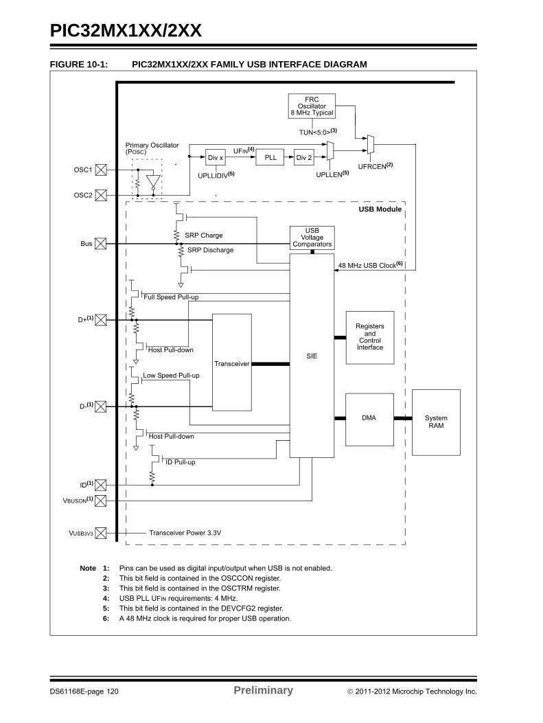
PIC32MX1XX/2XX
FIGURE 10-1: PIC32MX1XX/2XX FAMILY USB INTERFACE DIAGRAM
OSC1
OSC2
Primary Oscillator
8 MHz Typical
FRCOscillator
TUN<5:0>(3)
PLL
48 MHz USB Clock(6)
Div x
UPLLEN(5)UFRCEN(2)
(POSC)
UPLLIDIV(5)
UFIN(4)
Div 2
VUSB3V3
D+(1)
D-(1)
ID(1)
Bus
TransceiverSIE
VBUSON(1)
Comparators
USBSRP Charge
SRP Discharge
Registersand
ControlInterface
Transceiver Power 3.3V
USB Module
Voltage
SystemRAM
Full Speed Pull-up
Host Pull-down
Low Speed Pull-up
Host Pull-down
ID Pull-up
DMA
Note 1: Pins can be used as digital input/output when USB is not enabled.2: This bit field is contained in the OSCCON register.3: This bit field is contained in the OSCTRM register.4: USB PLL UFIN requirements: 4 MHz.5: This bit field is contained in the DEVCFG2 register.6: A 48 MHz clock is required for proper USB operation.
DS61168E-page 120 Preliminary 2011-2012 Microchip Technology Inc.
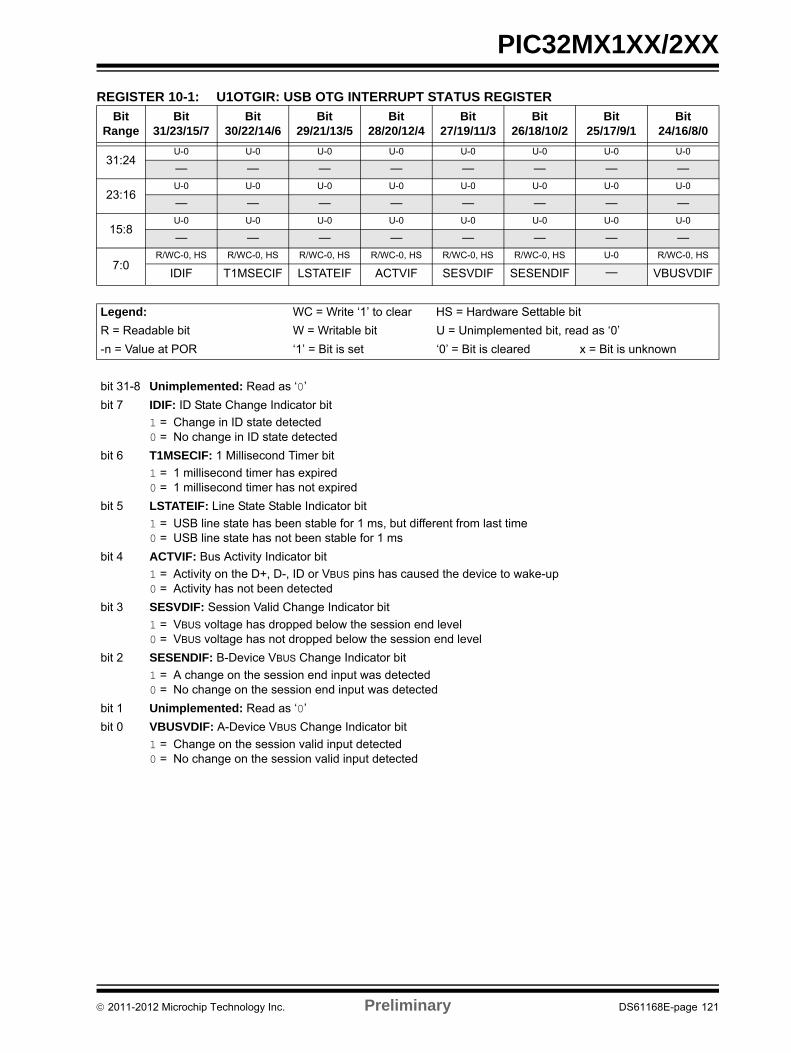
PIC32MX1XX/2XX
REGISTER 10-1: U1OTGIR: USB OTG INTERRUPT STATUS REGISTER
Bit Range
Bit31/23/15/7
Bit30/22/14/6
Bit29/21/13/5
Bit28/20/12/4
Bit27/19/11/3
Bit26/18/10/2
Bit25/17/9/1
Bit24/16/8/0
31:24U-0 U-0 U-0 U-0 U-0 U-0 U-0 U-0
— — — — — — — —
23:16U-0 U-0 U-0 U-0 U-0 U-0 U-0 U-0
— — — — — — — —
15:8U-0 U-0 U-0 U-0 U-0 U-0 U-0 U-0
— — — — — — — —
7:0R/WC-0, HS R/WC-0, HS R/WC-0, HS R/WC-0, HS R/WC-0, HS R/WC-0, HS U-0 R/WC-0, HS
IDIF T1MSECIF LSTATEIF ACTVIF SESVDIF SESENDIF — VBUSVDIF
Legend: WC = Write ‘1’ to clear HS = Hardware Settable bit
R = Readable bit W = Writable bit U = Unimplemented bit, read as ‘0’
-n = Value at POR ‘1’ = Bit is set ‘0’ = Bit is cleared x = Bit is unknown
bit 31-8 Unimplemented: Read as ‘0’
bit 7 IDIF: ID State Change Indicator bit
1 = Change in ID state detected0 = No change in ID state detected
bit 6 T1MSECIF: 1 Millisecond Timer bit
1 = 1 millisecond timer has expired0 = 1 millisecond timer has not expired
bit 5 LSTATEIF: Line State Stable Indicator bit
1 = USB line state has been stable for 1 ms, but different from last time0 = USB line state has not been stable for 1 ms
bit 4 ACTVIF: Bus Activity Indicator bit
1 = Activity on the D+, D-, ID or VBUS pins has caused the device to wake-up0 = Activity has not been detected
bit 3 SESVDIF: Session Valid Change Indicator bit
1 = VBUS voltage has dropped below the session end level0 = VBUS voltage has not dropped below the session end level
bit 2 SESENDIF: B-Device VBUS Change Indicator bit
1 = A change on the session end input was detected0 = No change on the session end input was detected
bit 1 Unimplemented: Read as ‘0’
bit 0 VBUSVDIF: A-Device VBUS Change Indicator bit
1 = Change on the session valid input detected0 = No change on the session valid input detected
2011-2012 Microchip Technology Inc. Preliminary DS61168E-page 121
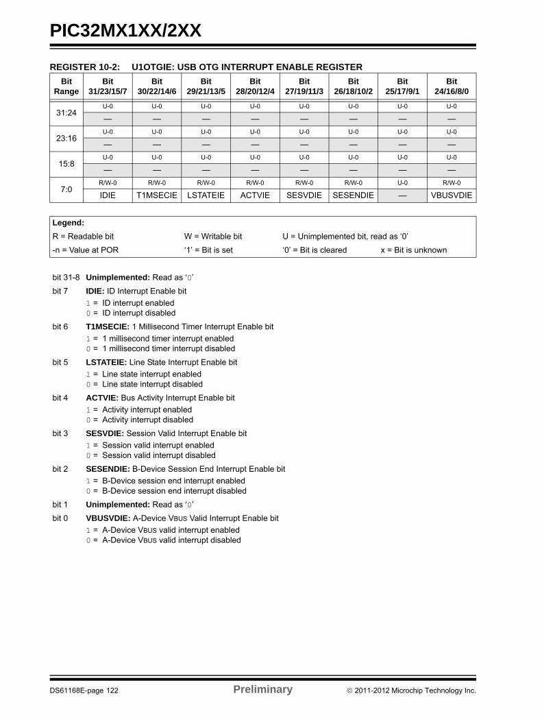
PIC32MX1XX/2XX
REGISTER 10-2: U1OTGIE: USB OTG INTERRUPT ENABLE REGISTER
Bit Range
Bit31/23/15/7
Bit30/22/14/6
Bit29/21/13/5
Bit28/20/12/4
Bit27/19/11/3
Bit26/18/10/2
Bit25/17/9/1
Bit24/16/8/0
31:24U-0 U-0 U-0 U-0 U-0 U-0 U-0 U-0
— — — — — — — —
23:16U-0 U-0 U-0 U-0 U-0 U-0 U-0 U-0
— — — — — — — —
15:8U-0 U-0 U-0 U-0 U-0 U-0 U-0 U-0
— — — — — — — —
7:0R/W-0 R/W-0 R/W-0 R/W-0 R/W-0 R/W-0 U-0 R/W-0
IDIE T1MSECIE LSTATEIE ACTVIE SESVDIE SESENDIE — VBUSVDIE
Legend:
R = Readable bit W = Writable bit U = Unimplemented bit, read as ‘0’
-n = Value at POR ‘1’ = Bit is set ‘0’ = Bit is cleared x = Bit is unknown
bit 31-8 Unimplemented: Read as ‘0’
bit 7 IDIE: ID Interrupt Enable bit
1 = ID interrupt enabled0 = ID interrupt disabled
bit 6 T1MSECIE: 1 Millisecond Timer Interrupt Enable bit
1 = 1 millisecond timer interrupt enabled0 = 1 millisecond timer interrupt disabled
bit 5 LSTATEIE: Line State Interrupt Enable bit
1 = Line state interrupt enabled0 = Line state interrupt disabled
bit 4 ACTVIE: Bus Activity Interrupt Enable bit
1 = Activity interrupt enabled0 = Activity interrupt disabled
bit 3 SESVDIE: Session Valid Interrupt Enable bit
1 = Session valid interrupt enabled0 = Session valid interrupt disabled
bit 2 SESENDIE: B-Device Session End Interrupt Enable bit
1 = B-Device session end interrupt enabled0 = B-Device session end interrupt disabled
bit 1 Unimplemented: Read as ‘0’
bit 0 VBUSVDIE: A-Device VBUS Valid Interrupt Enable bit
1 = A-Device VBUS valid interrupt enabled0 = A-Device VBUS valid interrupt disabled
DS61168E-page 122 Preliminary 2011-2012 Microchip Technology Inc.
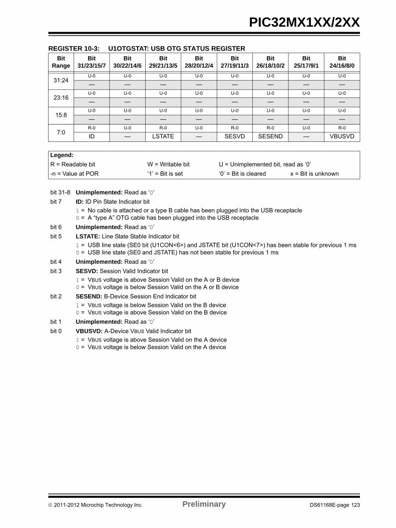
PIC32MX1XX/2XX
REGISTER 10-3: U1OTGSTAT: USB OTG STATUS REGISTER
Bit Range
Bit31/23/15/7
Bit30/22/14/6
Bit29/21/13/5
Bit28/20/12/4
Bit27/19/11/3
Bit26/18/10/2
Bit25/17/9/1
Bit24/16/8/0
31:24U-0 U-0 U-0 U-0 U-0 U-0 U-0 U-0
— — — — — — — —
23:16U-0 U-0 U-0 U-0 U-0 U-0 U-0 U-0
— — — — — — — —
15:8U-0 U-0 U-0 U-0 U-0 U-0 U-0 U-0
— — — — — — — —
7:0R-0 U-0 R-0 U-0 R-0 R-0 U-0 R-0
ID — LSTATE — SESVD SESEND — VBUSVD
Legend:
R = Readable bit W = Writable bit U = Unimplemented bit, read as ‘0’
-n = Value at POR ‘1’ = Bit is set ‘0’ = Bit is cleared x = Bit is unknown
bit 31-8 Unimplemented: Read as ‘0’
bit 7 ID: ID Pin State Indicator bit
1 = No cable is attached or a type B cable has been plugged into the USB receptacle0 = A “type A” OTG cable has been plugged into the USB receptacle
bit 6 Unimplemented: Read as ‘0’
bit 5 LSTATE: Line State Stable Indicator bit
1 = USB line state (SE0 bit (U1CON<6>) and JSTATE bit (U1CON<7>) has been stable for previous 1 ms0 = USB line state (SE0 and JSTATE) has not been stable for previous 1 ms
bit 4 Unimplemented: Read as ‘0’
bit 3 SESVD: Session Valid Indicator bit
1 = VBUS voltage is above Session Valid on the A or B device0 = VBUS voltage is below Session Valid on the A or B device
bit 2 SESEND: B-Device Session End Indicator bit
1 = VBUS voltage is below Session Valid on the B device0 = VBUS voltage is above Session Valid on the B device
bit 1 Unimplemented: Read as ‘0’
bit 0 VBUSVD: A-Device VBUS Valid Indicator bit
1 = VBUS voltage is above Session Valid on the A device0 = VBUS voltage is below Session Valid on the A device
2011-2012 Microchip Technology Inc. Preliminary DS61168E-page 123
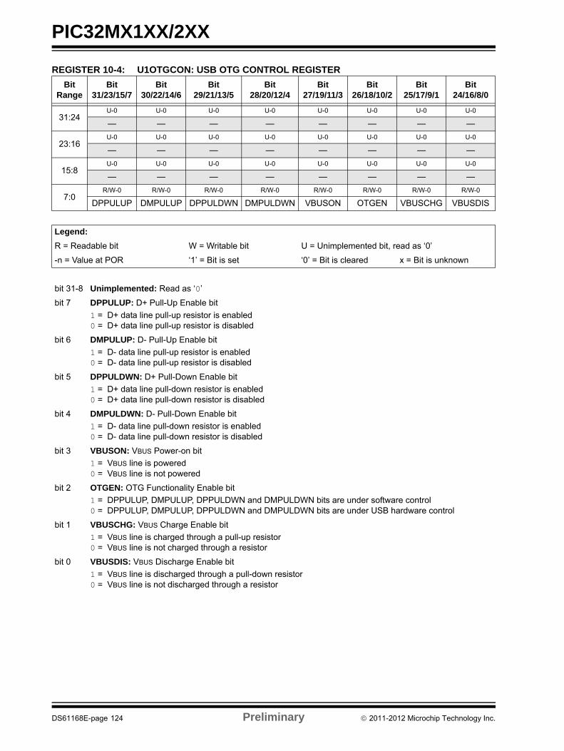
PIC32MX1XX/2XX
REGISTER 10-4: U1OTGCON: USB OTG CONTROL REGISTER
Bit Range
Bit31/23/15/7
Bit30/22/14/6
Bit29/21/13/5
Bit28/20/12/4
Bit27/19/11/3
Bit26/18/10/2
Bit25/17/9/1
Bit24/16/8/0
31:24U-0 U-0 U-0 U-0 U-0 U-0 U-0 U-0
— — — — — — — —
23:16U-0 U-0 U-0 U-0 U-0 U-0 U-0 U-0
— — — — — — — —
15:8U-0 U-0 U-0 U-0 U-0 U-0 U-0 U-0
— — — — — — — —
7:0R/W-0 R/W-0 R/W-0 R/W-0 R/W-0 R/W-0 R/W-0 R/W-0
DPPULUP DMPULUP DPPULDWN DMPULDWN VBUSON OTGEN VBUSCHG VBUSDIS
Legend:
R = Readable bit W = Writable bit U = Unimplemented bit, read as ‘0’
-n = Value at POR ‘1’ = Bit is set ‘0’ = Bit is cleared x = Bit is unknown
bit 31-8 Unimplemented: Read as ‘0’
bit 7 DPPULUP: D+ Pull-Up Enable bit
1 = D+ data line pull-up resistor is enabled0 = D+ data line pull-up resistor is disabled
bit 6 DMPULUP: D- Pull-Up Enable bit
1 = D- data line pull-up resistor is enabled0 = D- data line pull-up resistor is disabled
bit 5 DPPULDWN: D+ Pull-Down Enable bit
1 = D+ data line pull-down resistor is enabled0 = D+ data line pull-down resistor is disabled
bit 4 DMPULDWN: D- Pull-Down Enable bit
1 = D- data line pull-down resistor is enabled0 = D- data line pull-down resistor is disabled
bit 3 VBUSON: VBUS Power-on bit
1 = VBUS line is powered0 = VBUS line is not powered
bit 2 OTGEN: OTG Functionality Enable bit
1 = DPPULUP, DMPULUP, DPPULDWN and DMPULDWN bits are under software control0 = DPPULUP, DMPULUP, DPPULDWN and DMPULDWN bits are under USB hardware control
bit 1 VBUSCHG: VBUS Charge Enable bit
1 = VBUS line is charged through a pull-up resistor0 = VBUS line is not charged through a resistor
bit 0 VBUSDIS: VBUS Discharge Enable bit
1 = VBUS line is discharged through a pull-down resistor0 = VBUS line is not discharged through a resistor
DS61168E-page 124 Preliminary 2011-2012 Microchip Technology Inc.
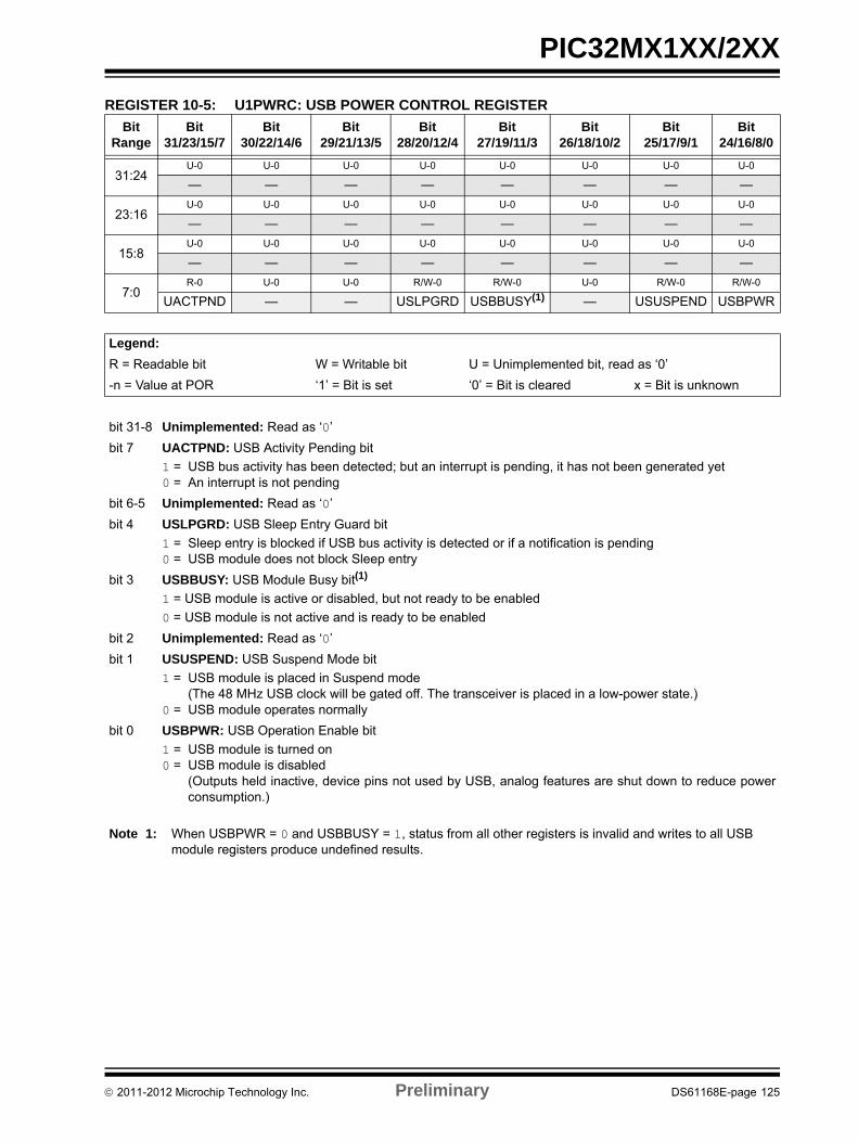
PIC32MX1XX/2XX
REGISTER 10-5: U1PWRC: USB POWER CONTROL REGISTER
Bit Range
Bit31/23/15/7
Bit30/22/14/6
Bit29/21/13/5
Bit28/20/12/4
Bit27/19/11/3
Bit26/18/10/2
Bit25/17/9/1
Bit24/16/8/0
31:24U-0 U-0 U-0 U-0 U-0 U-0 U-0 U-0
— — — — — — — —
23:16U-0 U-0 U-0 U-0 U-0 U-0 U-0 U-0
— — — — — — — —
15:8U-0 U-0 U-0 U-0 U-0 U-0 U-0 U-0
— — — — — — — —
7:0R-0 U-0 U-0 R/W-0 R/W-0 U-0 R/W-0 R/W-0
UACTPND — — USLPGRD USBBUSY(1) — USUSPEND USBPWR
Legend:
R = Readable bit W = Writable bit U = Unimplemented bit, read as ‘0’
-n = Value at POR ‘1’ = Bit is set ‘0’ = Bit is cleared x = Bit is unknown
bit 31-8 Unimplemented: Read as ‘0’
bit 7 UACTPND: USB Activity Pending bit
1 = USB bus activity has been detected; but an interrupt is pending, it has not been generated yet0 = An interrupt is not pending
bit 6-5 Unimplemented: Read as ‘0’
bit 4 USLPGRD: USB Sleep Entry Guard bit
1 = Sleep entry is blocked if USB bus activity is detected or if a notification is pending0 = USB module does not block Sleep entry
bit 3 USBBUSY: USB Module Busy bit(1)
1 = USB module is active or disabled, but not ready to be enabled
0 = USB module is not active and is ready to be enabled
bit 2 Unimplemented: Read as ‘0’
bit 1 USUSPEND: USB Suspend Mode bit
1 = USB module is placed in Suspend mode(The 48 MHz USB clock will be gated off. The transceiver is placed in a low-power state.)
0 = USB module operates normally
bit 0 USBPWR: USB Operation Enable bit
1 = USB module is turned on0 = USB module is disabled
(Outputs held inactive, device pins not used by USB, analog features are shut down to reduce powerconsumption.)
Note 1: When USBPWR = 0 and USBBUSY = 1, status from all other registers is invalid and writes to all USB module registers produce undefined results.
2011-2012 Microchip Technology Inc. Preliminary DS61168E-page 125
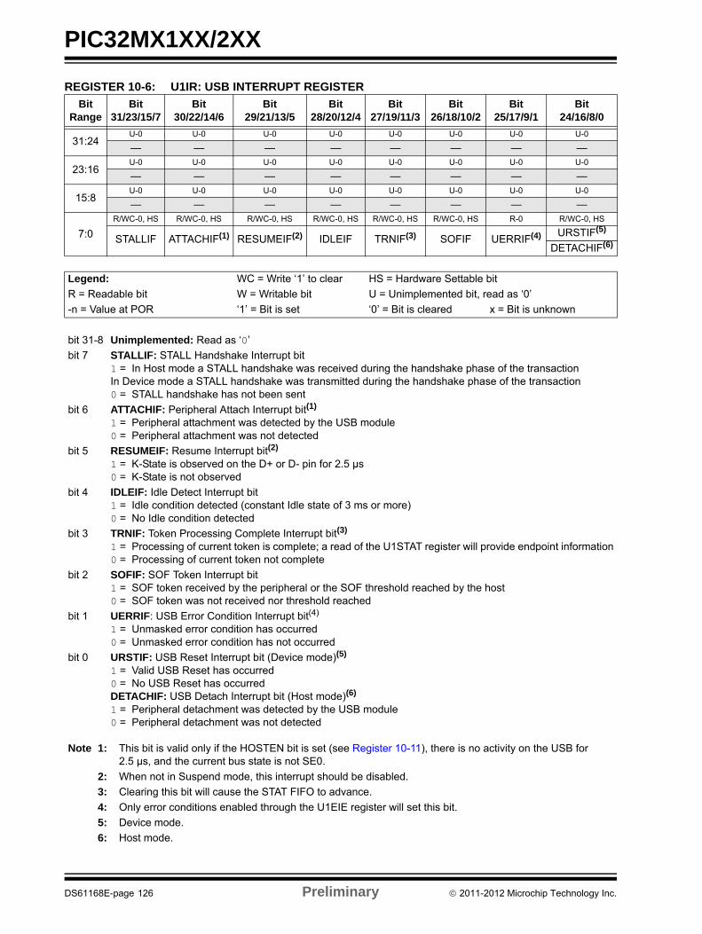
PIC32MX1XX/2XX
REGISTER 10-6: U1IR: USB INTERRUPT REGISTER
Bit Range
Bit31/23/15/7
Bit30/22/14/6
Bit29/21/13/5
Bit28/20/12/4
Bit27/19/11/3
Bit26/18/10/2
Bit25/17/9/1
Bit24/16/8/0
31:24U-0 U-0 U-0 U-0 U-0 U-0 U-0 U-0
— — — — — — — —
23:16U-0 U-0 U-0 U-0 U-0 U-0 U-0 U-0
— — — — — — — —
15:8U-0 U-0 U-0 U-0 U-0 U-0 U-0 U-0
— — — — — — — —
7:0
R/WC-0, HS R/WC-0, HS R/WC-0, HS R/WC-0, HS R/WC-0, HS R/WC-0, HS R-0 R/WC-0, HS
STALLIF ATTACHIF(1) RESUMEIF(2) IDLEIF TRNIF(3) SOFIF UERRIF(4) URSTIF(5)
DETACHIF(6)
Legend: WC = Write ‘1’ to clear HS = Hardware Settable bit
R = Readable bit W = Writable bit U = Unimplemented bit, read as ‘0’
-n = Value at POR ‘1’ = Bit is set ‘0’ = Bit is cleared x = Bit is unknown
bit 31-8 Unimplemented: Read as ‘0’
bit 7 STALLIF: STALL Handshake Interrupt bit1 = In Host mode a STALL handshake was received during the handshake phase of the transactionIn Device mode a STALL handshake was transmitted during the handshake phase of the transaction0 = STALL handshake has not been sent
bit 6 ATTACHIF: Peripheral Attach Interrupt bit(1)
1 = Peripheral attachment was detected by the USB module0 = Peripheral attachment was not detected
bit 5 RESUMEIF: Resume Interrupt bit(2)
1 = K-State is observed on the D+ or D- pin for 2.5 µs0 = K-State is not observed
bit 4 IDLEIF: Idle Detect Interrupt bit1 = Idle condition detected (constant Idle state of 3 ms or more)0 = No Idle condition detected
bit 3 TRNIF: Token Processing Complete Interrupt bit(3)
1 = Processing of current token is complete; a read of the U1STAT register will provide endpoint information0 = Processing of current token not complete
bit 2 SOFIF: SOF Token Interrupt bit1 = SOF token received by the peripheral or the SOF threshold reached by the host0 = SOF token was not received nor threshold reached
bit 1 UERRIF: USB Error Condition Interrupt bit(4)
1 = Unmasked error condition has occurred0 = Unmasked error condition has not occurred
bit 0 URSTIF: USB Reset Interrupt bit (Device mode)(5)
1 = Valid USB Reset has occurred0 = No USB Reset has occurredDETACHIF: USB Detach Interrupt bit (Host mode)(6)
1 = Peripheral detachment was detected by the USB module0 = Peripheral detachment was not detected
Note 1: This bit is valid only if the HOSTEN bit is set (see Register 10-11), there is no activity on the USB for 2.5 µs, and the current bus state is not SE0.
2: When not in Suspend mode, this interrupt should be disabled.
3: Clearing this bit will cause the STAT FIFO to advance.
4: Only error conditions enabled through the U1EIE register will set this bit.
5: Device mode.
6: Host mode.
DS61168E-page 126 Preliminary 2011-2012 Microchip Technology Inc.
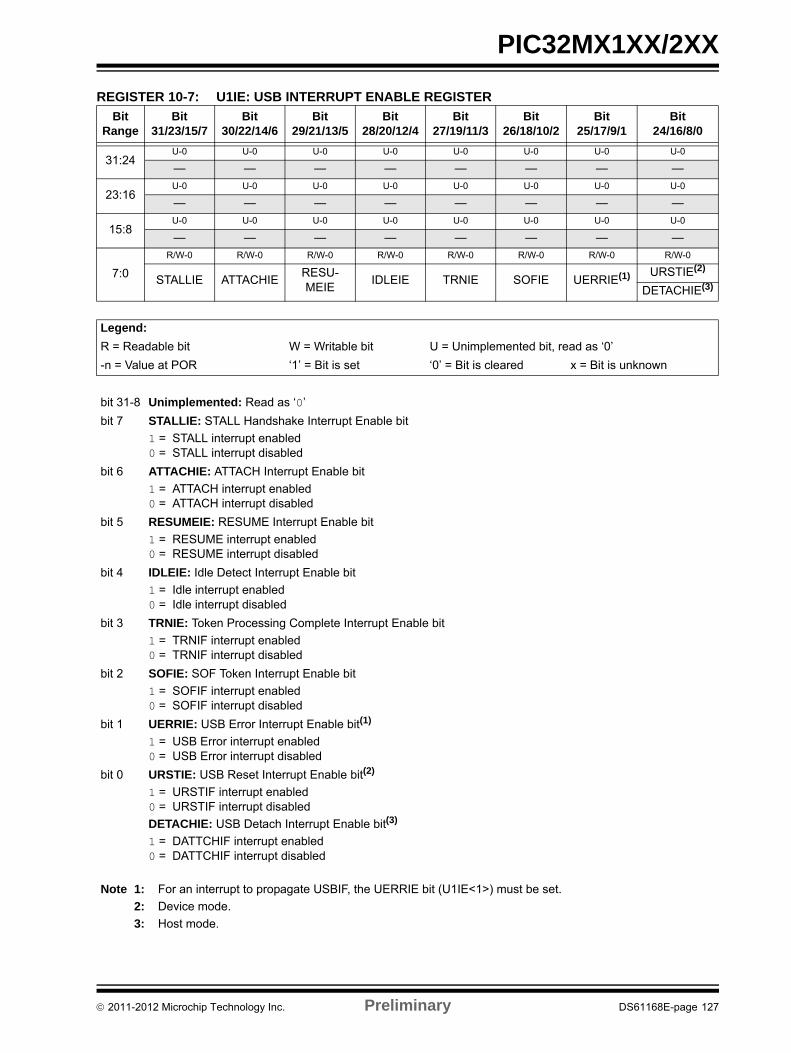
PIC32MX1XX/2XX
REGISTER 10-7: U1IE: USB INTERRUPT ENABLE REGISTER
Bit Range
Bit31/23/15/7
Bit30/22/14/6
Bit29/21/13/5
Bit28/20/12/4
Bit27/19/11/3
Bit26/18/10/2
Bit25/17/9/1
Bit24/16/8/0
31:24U-0 U-0 U-0 U-0 U-0 U-0 U-0 U-0
— — — — — — — —
23:16U-0 U-0 U-0 U-0 U-0 U-0 U-0 U-0
— — — — — — — —
15:8U-0 U-0 U-0 U-0 U-0 U-0 U-0 U-0
— — — — — — — —
7:0
R/W-0 R/W-0 R/W-0 R/W-0 R/W-0 R/W-0 R/W-0 R/W-0
STALLIE ATTACHIERESU-MEIE
IDLEIE TRNIE SOFIE UERRIE(1) URSTIE(2)
DETACHIE(3)
Legend:
R = Readable bit W = Writable bit U = Unimplemented bit, read as ‘0’
-n = Value at POR ‘1’ = Bit is set ‘0’ = Bit is cleared x = Bit is unknown
bit 31-8 Unimplemented: Read as ‘0’
bit 7 STALLIE: STALL Handshake Interrupt Enable bit
1 = STALL interrupt enabled0 = STALL interrupt disabled
bit 6 ATTACHIE: ATTACH Interrupt Enable bit
1 = ATTACH interrupt enabled0 = ATTACH interrupt disabled
bit 5 RESUMEIE: RESUME Interrupt Enable bit
1 = RESUME interrupt enabled0 = RESUME interrupt disabled
bit 4 IDLEIE: Idle Detect Interrupt Enable bit
1 = Idle interrupt enabled0 = Idle interrupt disabled
bit 3 TRNIE: Token Processing Complete Interrupt Enable bit
1 = TRNIF interrupt enabled0 = TRNIF interrupt disabled
bit 2 SOFIE: SOF Token Interrupt Enable bit
1 = SOFIF interrupt enabled0 = SOFIF interrupt disabled
bit 1 UERRIE: USB Error Interrupt Enable bit(1)
1 = USB Error interrupt enabled0 = USB Error interrupt disabled
bit 0 URSTIE: USB Reset Interrupt Enable bit(2)
1 = URSTIF interrupt enabled0 = URSTIF interrupt disabled
DETACHIE: USB Detach Interrupt Enable bit(3)
1 = DATTCHIF interrupt enabled0 = DATTCHIF interrupt disabled
Note 1: For an interrupt to propagate USBIF, the UERRIE bit (U1IE<1>) must be set.
2: Device mode.
3: Host mode.
2011-2012 Microchip Technology Inc. Preliminary DS61168E-page 127
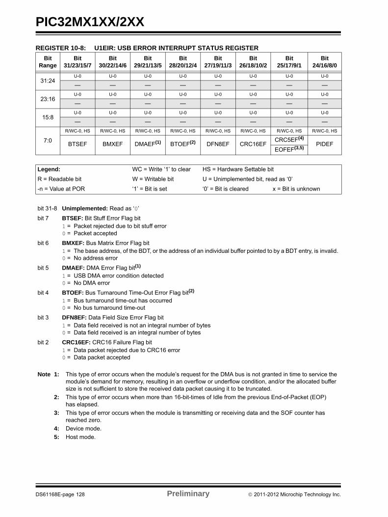
PIC32MX1XX/2XX
REGISTER 10-8: U1EIR: USB ERROR INTERRUPT STATUS REGISTER
Bit Range
Bit31/23/15/7
Bit30/22/14/6
Bit29/21/13/5
Bit28/20/12/4
Bit27/19/11/3
Bit26/18/10/2
Bit25/17/9/1
Bit24/16/8/0
31:24U-0 U-0 U-0 U-0 U-0 U-0 U-0 U-0
— — — — — — — —
23:16U-0 U-0 U-0 U-0 U-0 U-0 U-0 U-0
— — — — — — — —
15:8U-0 U-0 U-0 U-0 U-0 U-0 U-0 U-0
— — — — — — — —
7:0
R/WC-0, HS R/WC-0, HS R/WC-0, HS R/WC-0, HS R/WC-0, HS R/WC-0, HS R/WC-0, HS R/WC-0, HS
BTSEF BMXEF DMAEF(1) BTOEF(2) DFN8EF CRC16EFCRC5EF(4)
PIDEFEOFEF(3,5)
Legend: WC = Write ‘1’ to clear HS = Hardware Settable bit
R = Readable bit W = Writable bit U = Unimplemented bit, read as ‘0’
-n = Value at POR ‘1’ = Bit is set ‘0’ = Bit is cleared x = Bit is unknown
bit 31-8 Unimplemented: Read as ‘0’
bit 7 BTSEF: Bit Stuff Error Flag bit1 = Packet rejected due to bit stuff error0 = Packet accepted
bit 6 BMXEF: Bus Matrix Error Flag bit1 = The base address, of the BDT, or the address of an individual buffer pointed to by a BDT entry, is invalid. 0 = No address error
bit 5 DMAEF: DMA Error Flag bit(1)
1 = USB DMA error condition detected0 = No DMA error
bit 4 BTOEF: Bus Turnaround Time-Out Error Flag bit(2)
1 = Bus turnaround time-out has occurred0 = No bus turnaround time-out
bit 3 DFN8EF: Data Field Size Error Flag bit1 = Data field received is not an integral number of bytes0 = Data field received is an integral number of bytes
bit 2 CRC16EF: CRC16 Failure Flag bit1 = Data packet rejected due to CRC16 error0 = Data packet accepted
Note 1: This type of error occurs when the module’s request for the DMA bus is not granted in time to service the module’s demand for memory, resulting in an overflow or underflow condition, and/or the allocated buffer size is not sufficient to store the received data packet causing it to be truncated.
2: This type of error occurs when more than 16-bit-times of Idle from the previous End-of-Packet (EOP) has elapsed.
3: This type of error occurs when the module is transmitting or receiving data and the SOF counter has reached zero.
4: Device mode.
5: Host mode.
DS61168E-page 128 Preliminary 2011-2012 Microchip Technology Inc.
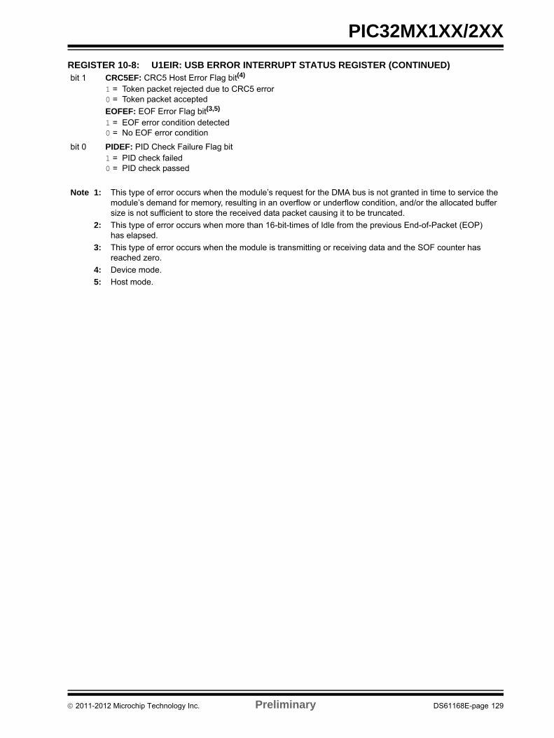
PIC32MX1XX/2XX
bit 1 CRC5EF: CRC5 Host Error Flag bit(4)
1 = Token packet rejected due to CRC5 error0 = Token packet accepted
EOFEF: EOF Error Flag bit(3,5)
1 = EOF error condition detected0 = No EOF error condition
bit 0 PIDEF: PID Check Failure Flag bit1 = PID check failed0 = PID check passed
REGISTER 10-8: U1EIR: USB ERROR INTERRUPT STATUS REGISTER (CONTINUED)
Note 1: This type of error occurs when the module’s request for the DMA bus is not granted in time to service the module’s demand for memory, resulting in an overflow or underflow condition, and/or the allocated buffer size is not sufficient to store the received data packet causing it to be truncated.
2: This type of error occurs when more than 16-bit-times of Idle from the previous End-of-Packet (EOP) has elapsed.
3: This type of error occurs when the module is transmitting or receiving data and the SOF counter has reached zero.
4: Device mode.
5: Host mode.
2011-2012 Microchip Technology Inc. Preliminary DS61168E-page 129
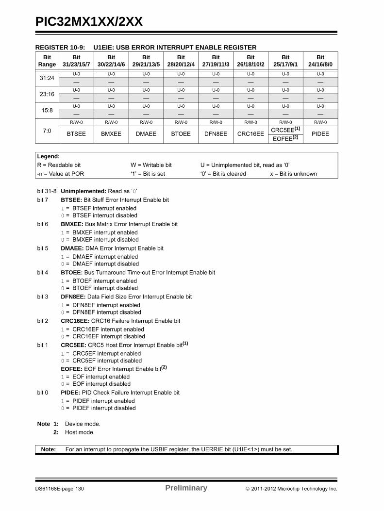
PIC32MX1XX/2XX
REGISTER 10-9: U1EIE: USB ERROR INTERRUPT ENABLE REGISTER
Bit Range
Bit31/23/15/7
Bit30/22/14/6
Bit29/21/13/5
Bit28/20/12/4
Bit27/19/11/3
Bit26/18/10/2
Bit25/17/9/1
Bit24/16/8/0
31:24U-0 U-0 U-0 U-0 U-0 U-0 U-0 U-0
— — — — — — — —
23:16U-0 U-0 U-0 U-0 U-0 U-0 U-0 U-0
— — — — — — — —
15:8U-0 U-0 U-0 U-0 U-0 U-0 U-0 U-0
— — — — — — — —
7:0
R/W-0 R/W-0 R/W-0 R/W-0 R/W-0 R/W-0 R/W-0 R/W-0
BTSEE BMXEE DMAEE BTOEE DFN8EE CRC16EECRC5EE(1)
PIDEEEOFEE(2)
Legend:
R = Readable bit W = Writable bit U = Unimplemented bit, read as ‘0’
-n = Value at POR ‘1’ = Bit is set ‘0’ = Bit is cleared x = Bit is unknown
bit 31-8 Unimplemented: Read as ‘0’
bit 7 BTSEE: Bit Stuff Error Interrupt Enable bit
1 = BTSEF interrupt enabled0 = BTSEF interrupt disabled
bit 6 BMXEE: Bus Matrix Error Interrupt Enable bit
1 = BMXEF interrupt enabled0 = BMXEF interrupt disabled
bit 5 DMAEE: DMA Error Interrupt Enable bit
1 = DMAEF interrupt enabled0 = DMAEF interrupt disabled
bit 4 BTOEE: Bus Turnaround Time-out Error Interrupt Enable bit
1 = BTOEF interrupt enabled0 = BTOEF interrupt disabled
bit 3 DFN8EE: Data Field Size Error Interrupt Enable bit
1 = DFN8EF interrupt enabled0 = DFN8EF interrupt disabled
bit 2 CRC16EE: CRC16 Failure Interrupt Enable bit
1 = CRC16EF interrupt enabled0 = CRC16EF interrupt disabled
bit 1 CRC5EE: CRC5 Host Error Interrupt Enable bit(1)
1 = CRC5EF interrupt enabled0 = CRC5EF interrupt disabled
EOFEE: EOF Error Interrupt Enable bit(2)
1 = EOF interrupt enabled0 = EOF interrupt disabled
bit 0 PIDEE: PID Check Failure Interrupt Enable bit
1 = PIDEF interrupt enabled0 = PIDEF interrupt disabled
Note 1: Device mode.
2: Host mode.
Note: For an interrupt to propagate the USBIF register, the UERRIE bit (U1IE<1>) must be set.
DS61168E-page 130 Preliminary 2011-2012 Microchip Technology Inc.
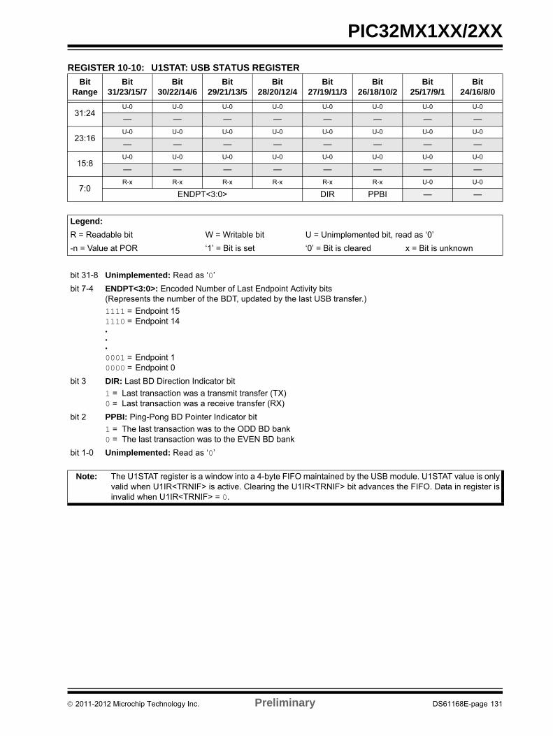
PIC32MX1XX/2XX
REGISTER 10-10: U1STAT: USB STATUS REGISTER
Bit Range
Bit31/23/15/7
Bit30/22/14/6
Bit29/21/13/5
Bit28/20/12/4
Bit27/19/11/3
Bit26/18/10/2
Bit25/17/9/1
Bit24/16/8/0
31:24U-0 U-0 U-0 U-0 U-0 U-0 U-0 U-0
— — — — — — — —
23:16U-0 U-0 U-0 U-0 U-0 U-0 U-0 U-0
— — — — — — — —
15:8U-0 U-0 U-0 U-0 U-0 U-0 U-0 U-0
— — — — — — — —
7:0R-x R-x R-x R-x R-x R-x U-0 U-0
ENDPT<3:0> DIR PPBI — —
Legend:
R = Readable bit W = Writable bit U = Unimplemented bit, read as ‘0’
-n = Value at POR ‘1’ = Bit is set ‘0’ = Bit is cleared x = Bit is unknown
bit 31-8 Unimplemented: Read as ‘0’
bit 7-4 ENDPT<3:0>: Encoded Number of Last Endpoint Activity bits(Represents the number of the BDT, updated by the last USB transfer.)
1111 = Endpoint 151110 = Endpoint 14•••
0001 = Endpoint 10000 = Endpoint 0
bit 3 DIR: Last BD Direction Indicator bit
1 = Last transaction was a transmit transfer (TX)0 = Last transaction was a receive transfer (RX)
bit 2 PPBI: Ping-Pong BD Pointer Indicator bit
1 = The last transaction was to the ODD BD bank0 = The last transaction was to the EVEN BD bank
bit 1-0 Unimplemented: Read as ‘0’
Note: The U1STAT register is a window into a 4-byte FIFO maintained by the USB module. U1STAT value is onlyvalid when U1IR<TRNIF> is active. Clearing the U1IR<TRNIF> bit advances the FIFO. Data in register isinvalid when U1IR<TRNIF> = 0.
2011-2012 Microchip Technology Inc. Preliminary DS61168E-page 131
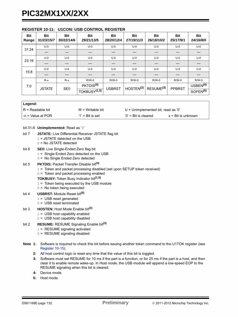
PIC32MX1XX/2XX
REGISTER 10-11: U1CON: USB CONTROL REGISTER
Bit Range
Bit31/23/15/7
Bit30/22/14/6
Bit29/21/13/5
Bit28/20/12/4
Bit27/19/11/3
Bit26/18/10/2
Bit25/17/9/1
Bit24/16/8/0
31:24U-0 U-0 U-0 U-0 U-0 U-0 U-0 U-0
— — — — — — — —
23:16U-0 U-0 U-0 U-0 U-0 U-0 U-0 U-0
— — — — — — — —
15:8U-0 U-0 U-0 U-0 U-0 U-0 U-0 U-0
— — — — — — — —
7:0
R-x R-x R/W-0 R/W-0 R/W-0 R/W-0 R/W-0 R/W-0
JSTATE SE0PKTDIS(4)
USBRST HOSTEN(2) RESUME(3) PPBRSTUSBEN(4)
TOKBUSY(1,5) SOFEN(5)
Legend:
R = Readable bit W = Writable bit U = Unimplemented bit, read as ‘0’
-n = Value at POR ‘1’ = Bit is set ‘0’ = Bit is cleared x = Bit is unknown
bit 31-8 Unimplemented: Read as ‘0’
bit 7 JSTATE: Live Differential Receiver JSTATE flag bit1 = JSTATE detected on the USB0 = No JSTATE detected
bit 6 SE0: Live Single-Ended Zero flag bit1 = Single Ended Zero detected on the USB0 = No Single Ended Zero detected
bit 5 PKTDIS: Packet Transfer Disable bit(4)
1 = Token and packet processing disabled (set upon SETUP token received)0 = Token and packet processing enabled
TOKBUSY: Token Busy Indicator bit(1,5)
1 = Token being executed by the USB module0 = No token being executed
bit 4 USBRST: Module Reset bit(5)
1 = USB reset generated0 = USB reset terminated
bit 3 HOSTEN: Host Mode Enable bit(2)
1 = USB host capability enabled0 = USB host capability disabled
bit 2 RESUME: RESUME Signaling Enable bit(3)
1 = RESUME signaling activated0 = RESUME signaling disabled
Note 1: Software is required to check this bit before issuing another token command to the U1TOK register (see Register 10-15).
2: All host control logic is reset any time that the value of this bit is toggled.
3: Software must set RESUME for 10 ms if the part is a function, or for 25 ms if the part is a host, and then clear it to enable remote wake-up. In Host mode, the USB module will append a low-speed EOP to the RESUME signaling when this bit is cleared.
4: Device mode.
5: Host mode.
DS61168E-page 132 Preliminary 2011-2012 Microchip Technology Inc.
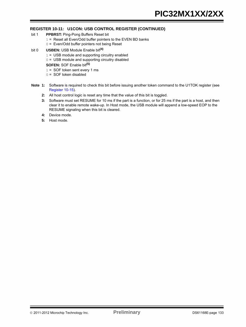
PIC32MX1XX/2XX
bit 1 PPBRST: Ping-Pong Buffers Reset bit1 = Reset all Even/Odd buffer pointers to the EVEN BD banks0 = Even/Odd buffer pointers not being Reset
bit 0 USBEN: USB Module Enable bit(4)
1 = USB module and supporting circuitry enabled0 = USB module and supporting circuitry disabled
SOFEN: SOF Enable bit(5)
1 = SOF token sent every 1 ms0 = SOF token disabled
REGISTER 10-11: U1CON: USB CONTROL REGISTER (CONTINUED)
Note 1: Software is required to check this bit before issuing another token command to the U1TOK register (see Register 10-15).
2: All host control logic is reset any time that the value of this bit is toggled.
3: Software must set RESUME for 10 ms if the part is a function, or for 25 ms if the part is a host, and then clear it to enable remote wake-up. In Host mode, the USB module will append a low-speed EOP to the RESUME signaling when this bit is cleared.
4: Device mode.
5: Host mode.
2011-2012 Microchip Technology Inc. Preliminary DS61168E-page 133
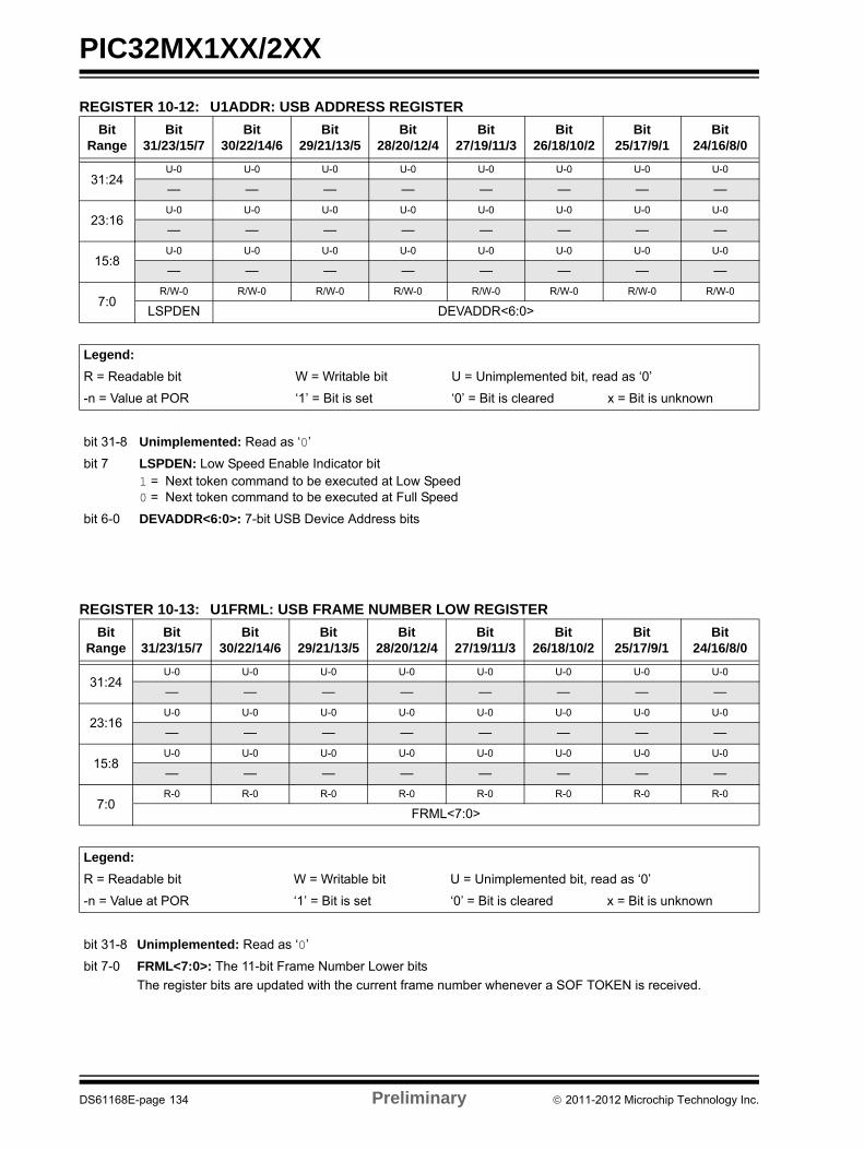
PIC32MX1XX/2XX
REGISTER 10-12: U1ADDR: USB ADDRESS REGISTER
Bit Range
Bit31/23/15/7
Bit30/22/14/6
Bit29/21/13/5
Bit28/20/12/4
Bit27/19/11/3
Bit26/18/10/2
Bit25/17/9/1
Bit24/16/8/0
31:24U-0 U-0 U-0 U-0 U-0 U-0 U-0 U-0
— — — — — — — —
23:16U-0 U-0 U-0 U-0 U-0 U-0 U-0 U-0
— — — — — — — —
15:8U-0 U-0 U-0 U-0 U-0 U-0 U-0 U-0
— — — — — — — —
7:0R/W-0 R/W-0 R/W-0 R/W-0 R/W-0 R/W-0 R/W-0 R/W-0
LSPDEN DEVADDR<6:0>
Legend:
R = Readable bit W = Writable bit U = Unimplemented bit, read as ‘0’
-n = Value at POR ‘1’ = Bit is set ‘0’ = Bit is cleared x = Bit is unknown
bit 31-8 Unimplemented: Read as ‘0’
bit 7 LSPDEN: Low Speed Enable Indicator bit1 = Next token command to be executed at Low Speed0 = Next token command to be executed at Full Speed
bit 6-0 DEVADDR<6:0>: 7-bit USB Device Address bits
REGISTER 10-13: U1FRML: USB FRAME NUMBER LOW REGISTER
Bit Range
Bit31/23/15/7
Bit30/22/14/6
Bit29/21/13/5
Bit28/20/12/4
Bit27/19/11/3
Bit26/18/10/2
Bit25/17/9/1
Bit24/16/8/0
31:24U-0 U-0 U-0 U-0 U-0 U-0 U-0 U-0
— — — — — — — —
23:16U-0 U-0 U-0 U-0 U-0 U-0 U-0 U-0
— — — — — — — —
15:8U-0 U-0 U-0 U-0 U-0 U-0 U-0 U-0
— — — — — — — —
7:0R-0 R-0 R-0 R-0 R-0 R-0 R-0 R-0
FRML<7:0>
Legend:
R = Readable bit W = Writable bit U = Unimplemented bit, read as ‘0’
-n = Value at POR ‘1’ = Bit is set ‘0’ = Bit is cleared x = Bit is unknown
bit 31-8 Unimplemented: Read as ‘0’
bit 7-0 FRML<7:0>: The 11-bit Frame Number Lower bits
The register bits are updated with the current frame number whenever a SOF TOKEN is received.
DS61168E-page 134 Preliminary 2011-2012 Microchip Technology Inc.
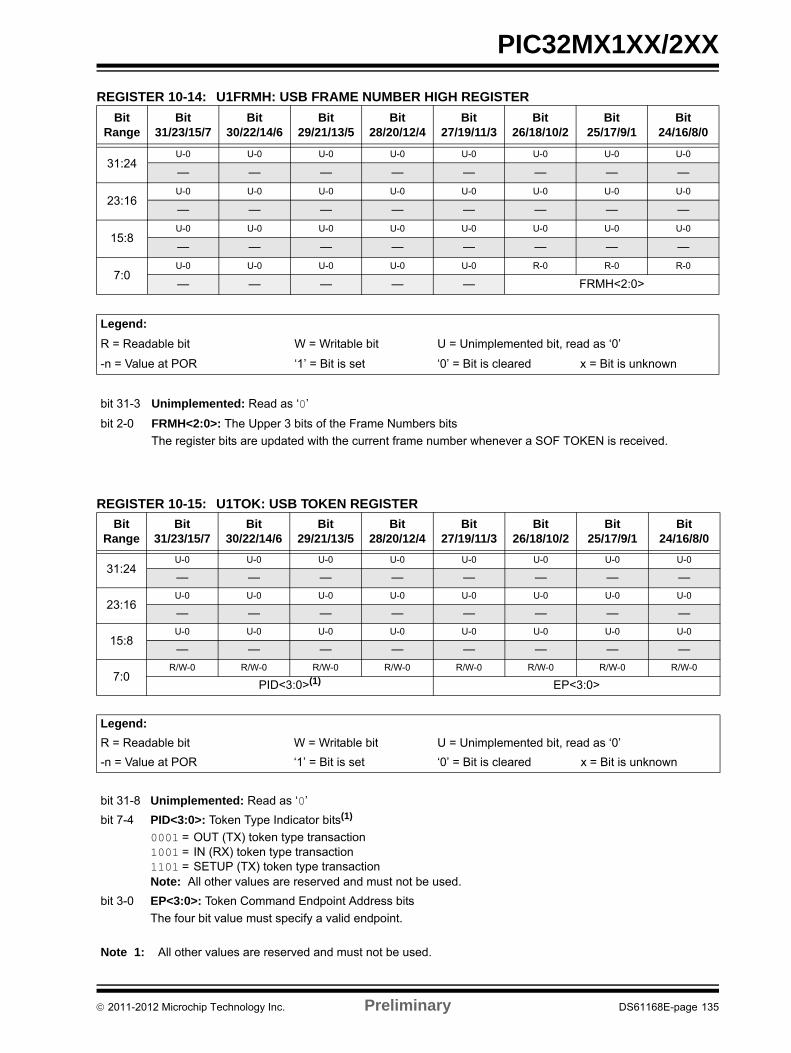
PIC32MX1XX/2XX
REGISTER 10-14: U1FRMH: USB FRAME NUMBER HIGH REGISTER
Bit Range
Bit31/23/15/7
Bit30/22/14/6
Bit29/21/13/5
Bit28/20/12/4
Bit27/19/11/3
Bit26/18/10/2
Bit25/17/9/1
Bit24/16/8/0
31:24U-0 U-0 U-0 U-0 U-0 U-0 U-0 U-0
— — — — — — — —
23:16U-0 U-0 U-0 U-0 U-0 U-0 U-0 U-0
— — — — — — — —
15:8U-0 U-0 U-0 U-0 U-0 U-0 U-0 U-0
— — — — — — — —
7:0U-0 U-0 U-0 U-0 U-0 R-0 R-0 R-0
— — — — — FRMH<2:0>
Legend:
R = Readable bit W = Writable bit U = Unimplemented bit, read as ‘0’
-n = Value at POR ‘1’ = Bit is set ‘0’ = Bit is cleared x = Bit is unknown
bit 31-3 Unimplemented: Read as ‘0’
bit 2-0 FRMH<2:0>: The Upper 3 bits of the Frame Numbers bits
The register bits are updated with the current frame number whenever a SOF TOKEN is received.
REGISTER 10-15: U1TOK: USB TOKEN REGISTER
Bit Range
Bit31/23/15/7
Bit30/22/14/6
Bit29/21/13/5
Bit28/20/12/4
Bit27/19/11/3
Bit26/18/10/2
Bit25/17/9/1
Bit24/16/8/0
31:24U-0 U-0 U-0 U-0 U-0 U-0 U-0 U-0
— — — — — — — —
23:16U-0 U-0 U-0 U-0 U-0 U-0 U-0 U-0
— — — — — — — —
15:8U-0 U-0 U-0 U-0 U-0 U-0 U-0 U-0
— — — — — — — —
7:0R/W-0 R/W-0 R/W-0 R/W-0 R/W-0 R/W-0 R/W-0 R/W-0
PID<3:0>(1) EP<3:0>
Legend:
R = Readable bit W = Writable bit U = Unimplemented bit, read as ‘0’
-n = Value at POR ‘1’ = Bit is set ‘0’ = Bit is cleared x = Bit is unknown
bit 31-8 Unimplemented: Read as ‘0’
bit 7-4 PID<3:0>: Token Type Indicator bits(1)
0001 = OUT (TX) token type transaction1001 = IN (RX) token type transaction1101 = SETUP (TX) token type transactionNote: All other values are reserved and must not be used.
bit 3-0 EP<3:0>: Token Command Endpoint Address bits
The four bit value must specify a valid endpoint.
Note 1: All other values are reserved and must not be used.
2011-2012 Microchip Technology Inc. Preliminary DS61168E-page 135
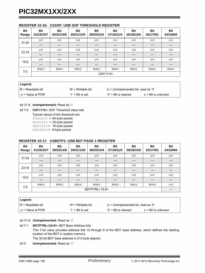
PIC32MX1XX/2XX
REGISTER 10-16: U1SOF: USB SOF THRESHOLD REGISTER
Bit Range
Bit31/23/15/7
Bit30/22/14/6
Bit29/21/13/5
Bit28/20/12/4
Bit27/19/11/3
Bit26/18/10/2
Bit25/17/9/1
Bit24/16/8/0
31:24U-0 U-0 U-0 U-0 U-0 U-0 U-0 U-0
— — — — — — — —
23:16U-0 U-0 U-0 U-0 U-0 U-0 U-0 U-0
— — — — — — — —
15:8U-0 U-0 U-0 U-0 U-0 U-0 U-0 U-0
— — — — — — — —
7:0R/W-0 R/W-0 R/W-0 R/W-0 R/W-0 R/W-0 R/W-0 R/W-0
CNT<7:0>
Legend:
R = Readable bit W = Writable bit U = Unimplemented bit, read as ‘0’
-n = Value at POR ‘1’ = Bit is set ‘0’ = Bit is cleared x = Bit is unknown
bit 31-8 Unimplemented: Read as ‘0’
bit 7-0 CNT<7:0>: SOF Threshold Value bits
Typical values of the threshold are:01001010 = 64-byte packet00101010 = 32-byte packet00011010 = 16-byte packet00010010 = 8-byte packet
REGISTER 10-17: U1BDTP1: USB BDT PAGE 1 REGISTER
Bit Range
Bit31/23/15/7
Bit30/22/14/6
Bit29/21/13/5
Bit28/20/12/4
Bit27/19/11/3
Bit26/18/10/2
Bit25/17/9/1
Bit24/16/8/0
31:24U-0 U-0 U-0 U-0 U-0 U-0 U-0 U-0
— — — — — — — —
23:16U-0 U-0 U-0 U-0 U-0 U-0 U-0 U-0
— — — — — — — —
15:8U-0 U-0 U-0 U-0 U-0 U-0 U-0 U-0
— — — — — — — —
7:0R/W-0 R/W-0 R/W-0 R/W-0 R/W-0 R/W-0 R/W-0 U-0
BDTPTRL<15:9> —
Legend:
R = Readable bit W = Writable bit U = Unimplemented bit, read as ‘0’
-n = Value at POR ‘1’ = Bit is set ‘0’ = Bit is cleared x = Bit is unknown
bit 31-8 Unimplemented: Read as ‘0’
bit 7-1 BDTPTRL<15:9>: BDT Base Address bits
This 7-bit value provides address bits 15 through 9 of the BDT base address, which defines the startinglocation of the BDT in system memory.
The 32-bit BDT base address is 512-byte aligned.
bit 0 Unimplemented: Read as ‘0’
DS61168E-page 136 Preliminary 2011-2012 Microchip Technology Inc.
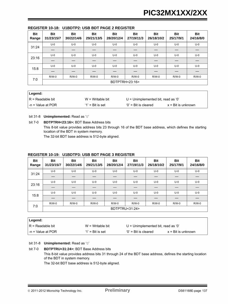
PIC32MX1XX/2XX
REGISTER 10-18: U1BDTP2: USB BDT PAGE 2 REGISTER
Bit Range
Bit31/23/15/7
Bit30/22/14/6
Bit29/21/13/5
Bit28/20/12/4
Bit27/19/11/3
Bit26/18/10/2
Bit25/17/9/1
Bit24/16/8/0
31:24U-0 U-0 U-0 U-0 U-0 U-0 U-0 U-0
— — — — — — — —
23:16U-0 U-0 U-0 U-0 U-0 U-0 U-0 U-0
— — — — — — — —
15:8U-0 U-0 U-0 U-0 U-0 U-0 U-0 U-0
— — — — — — — —
7:0R/W-0 R/W-0 R/W-0 R/W-0 R/W-0 R/W-0 R/W-0 R/W-0
BDTPTRH<23:16>
Legend:
R = Readable bit W = Writable bit U = Unimplemented bit, read as ‘0’
-n = Value at POR ‘1’ = Bit is set ‘0’ = Bit is cleared x = Bit is unknown
bit 31-8 Unimplemented: Read as ‘0’
bit 7-0 BDTPTRH<23:16>: BDT Base Address bits
This 8-bit value provides address bits 23 through 16 of the BDT base address, which defines the startinglocation of the BDT in system memory.
The 32-bit BDT base address is 512-byte aligned.
REGISTER 10-19: U1BDTP3: USB BDT PAGE 3 REGISTER
Bit Range
Bit31/23/15/7
Bit30/22/14/6
Bit29/21/13/5
Bit28/20/12/4
Bit27/19/11/3
Bit26/18/10/2
Bit25/17/9/1
Bit24/16/8/0
31:24U-0 U-0 U-0 U-0 U-0 U-0 U-0 U-0
— — — — — — — —
23:16U-0 U-0 U-0 U-0 U-0 U-0 U-0 U-0
— — — — — — — —
15:8U-0 U-0 U-0 U-0 U-0 U-0 U-0 U-0
— — — — — — — —
7:0R/W-0 R/W-0 R/W-0 R/W-0 R/W-0 R/W-0 R/W-0 R/W-0
BDTPTRU<31:24>
Legend:
R = Readable bit W = Writable bit U = Unimplemented bit, read as ‘0’
-n = Value at POR ‘1’ = Bit is set ‘0’ = Bit is cleared x = Bit is unknown
bit 31-8 Unimplemented: Read as ‘0’
bit 7-0 BDTPTRU<31:24>: BDT Base Address bits
This 8-bit value provides address bits 31 through 24 of the BDT base address, defines the starting locationof the BDT in system memory.
The 32-bit BDT base address is 512-byte aligned.
2011-2012 Microchip Technology Inc. Preliminary DS61168E-page 137
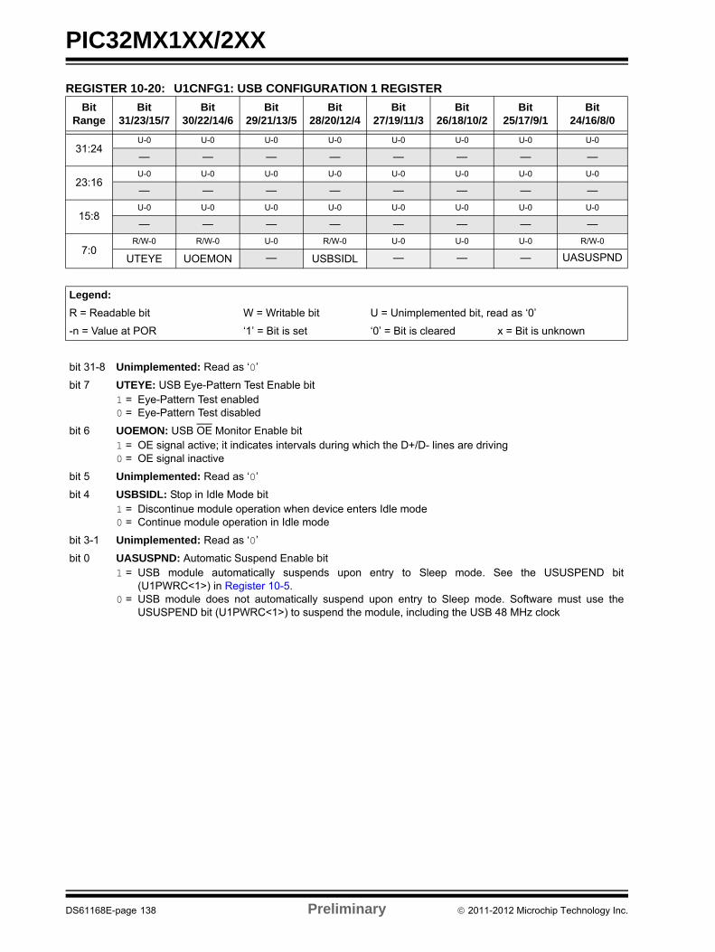
PIC32MX1XX/2XX
REGISTER 10-20: U1CNFG1: USB CONFIGURATION 1 REGISTER
Bit Range
Bit31/23/15/7
Bit30/22/14/6
Bit29/21/13/5
Bit28/20/12/4
Bit27/19/11/3
Bit26/18/10/2
Bit25/17/9/1
Bit24/16/8/0
31:24U-0 U-0 U-0 U-0 U-0 U-0 U-0 U-0
— — — — — — — —
23:16U-0 U-0 U-0 U-0 U-0 U-0 U-0 U-0
— — — — — — — —
15:8U-0 U-0 U-0 U-0 U-0 U-0 U-0 U-0
— — — — — — — —
7:0R/W-0 R/W-0 U-0 R/W-0 U-0 U-0 U-0 R/W-0
UTEYE UOEMON — USBSIDL — — — UASUSPND
Legend:
R = Readable bit W = Writable bit U = Unimplemented bit, read as ‘0’
-n = Value at POR ‘1’ = Bit is set ‘0’ = Bit is cleared x = Bit is unknown
bit 31-8 Unimplemented: Read as ‘0’
bit 7 UTEYE: USB Eye-Pattern Test Enable bit1 = Eye-Pattern Test enabled0 = Eye-Pattern Test disabled
bit 6 UOEMON: USB OE Monitor Enable bit1 = OE signal active; it indicates intervals during which the D+/D- lines are driving0 = OE signal inactive
bit 5 Unimplemented: Read as ‘0’
bit 4 USBSIDL: Stop in Idle Mode bit1 = Discontinue module operation when device enters Idle mode0 = Continue module operation in Idle mode
bit 3-1 Unimplemented: Read as ‘0’
bit 0 UASUSPND: Automatic Suspend Enable bit1 = USB module automatically suspends upon entry to Sleep mode. See the USUSPEND bit
(U1PWRC<1>) in Register 10-5.0 = USB module does not automatically suspend upon entry to Sleep mode. Software must use the
USUSPEND bit (U1PWRC<1>) to suspend the module, including the USB 48 MHz clock
DS61168E-page 138 Preliminary 2011-2012 Microchip Technology Inc.
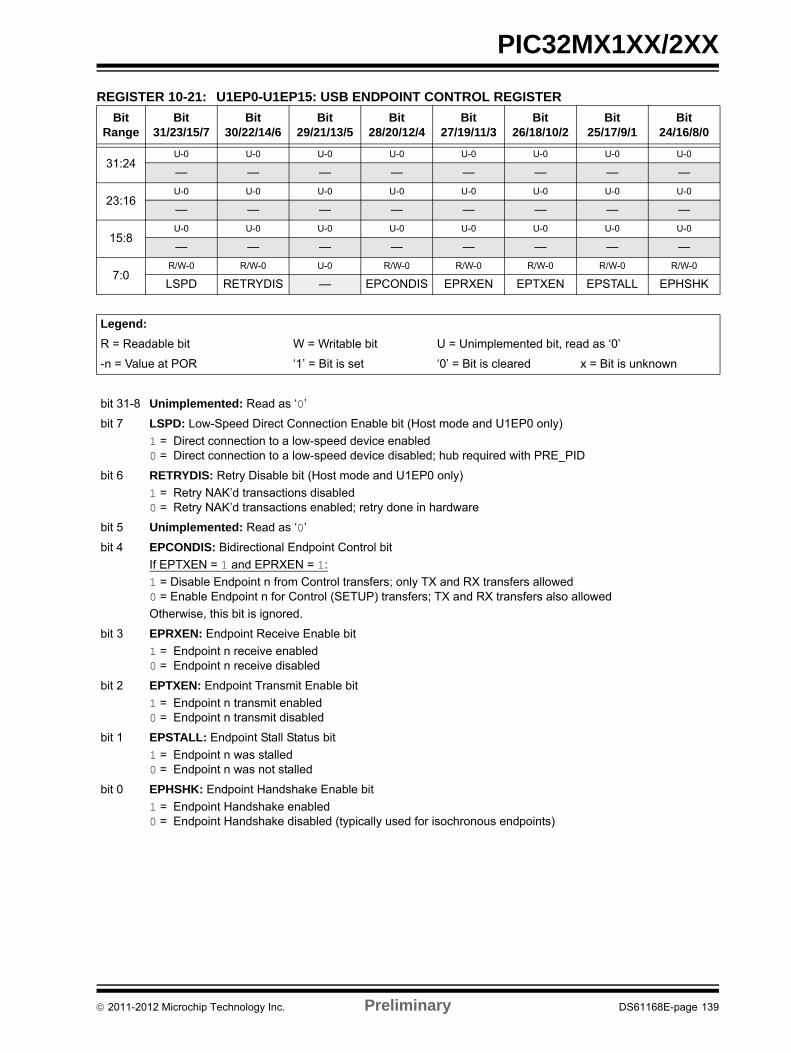
PIC32MX1XX/2XX
REGISTER 10-21: U1EP0-U1EP15: USB ENDPOINT CONTROL REGISTER
Bit Range
Bit31/23/15/7
Bit30/22/14/6
Bit29/21/13/5
Bit28/20/12/4
Bit27/19/11/3
Bit26/18/10/2
Bit25/17/9/1
Bit24/16/8/0
31:24U-0 U-0 U-0 U-0 U-0 U-0 U-0 U-0
— — — — — — — —
23:16U-0 U-0 U-0 U-0 U-0 U-0 U-0 U-0
— — — — — — — —
15:8U-0 U-0 U-0 U-0 U-0 U-0 U-0 U-0
— — — — — — — —
7:0R/W-0 R/W-0 U-0 R/W-0 R/W-0 R/W-0 R/W-0 R/W-0
LSPD RETRYDIS — EPCONDIS EPRXEN EPTXEN EPSTALL EPHSHK
Legend:
R = Readable bit W = Writable bit U = Unimplemented bit, read as ‘0’
-n = Value at POR ‘1’ = Bit is set ‘0’ = Bit is cleared x = Bit is unknown
bit 31-8 Unimplemented: Read as ‘0’
bit 7 LSPD: Low-Speed Direct Connection Enable bit (Host mode and U1EP0 only)
1 = Direct connection to a low-speed device enabled0 = Direct connection to a low-speed device disabled; hub required with PRE_PID
bit 6 RETRYDIS: Retry Disable bit (Host mode and U1EP0 only)
1 = Retry NAK’d transactions disabled0 = Retry NAK’d transactions enabled; retry done in hardware
bit 5 Unimplemented: Read as ‘0’
bit 4 EPCONDIS: Bidirectional Endpoint Control bit
If EPTXEN = 1 and EPRXEN = 1:
1 = Disable Endpoint n from Control transfers; only TX and RX transfers allowed0 = Enable Endpoint n for Control (SETUP) transfers; TX and RX transfers also allowed
Otherwise, this bit is ignored.
bit 3 EPRXEN: Endpoint Receive Enable bit
1 = Endpoint n receive enabled0 = Endpoint n receive disabled
bit 2 EPTXEN: Endpoint Transmit Enable bit
1 = Endpoint n transmit enabled0 = Endpoint n transmit disabled
bit 1 EPSTALL: Endpoint Stall Status bit
1 = Endpoint n was stalled0 = Endpoint n was not stalled
bit 0 EPHSHK: Endpoint Handshake Enable bit
1 = Endpoint Handshake enabled0 = Endpoint Handshake disabled (typically used for isochronous endpoints)
2011-2012 Microchip Technology Inc. Preliminary DS61168E-page 139

PIC32MX1XX/2XX
NOTES:
DS61168E-page 140 Preliminary 2011-2012 Microchip Technology Inc.
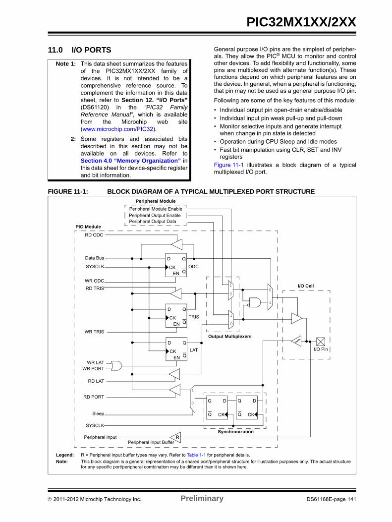
PIC32MX1XX/2XX
11.0 I/O PORTS General purpose I/O pins are the simplest of peripher-als. They allow the PIC® MCU to monitor and controlother devices. To add flexibility and functionality, somepins are multiplexed with alternate function(s). Thesefunctions depend on which peripheral features are onthe device. In general, when a peripheral is functioning,that pin may not be used as a general purpose I/O pin.
Following are some of the key features of this module:
• Individual output pin open-drain enable/disable• Individual input pin weak pull-up and pull-down• Monitor selective inputs and generate interrupt
when change in pin state is detected• Operation during CPU Sleep and Idle modes• Fast bit manipulation using CLR, SET and INV
registersFigure 11-1 illustrates a block diagram of a typicalmultiplexed I/O port.
FIGURE 11-1: BLOCK DIAGRAM OF A TYPICAL MULTIPLEXED PORT STRUCTURE
Note 1: This data sheet summarizes the featuresof the PIC32MX1XX/2XX family ofdevices. It is not intended to be acomprehensive reference source. Tocomplement the information in this datasheet, refer to Section 12. “I/O Ports”(DS61120) in the “PIC32 FamilyReference Manual”, which is availablefrom the Microchip web site(www.microchip.com/PIC32).
2: Some registers and associated bitsdescribed in this section may not beavailable on all devices. Refer toSection 4.0 “Memory Organization” inthis data sheet for device-specific registerand bit information.
Peripheral Output Data
Peripheral Module
Peripheral Output Enable
PIO Module
Peripheral Module Enable
WR LAT
I/O Pin
WR PORT
Data Bus
RD LAT
RD PORT
RD TRIS
WR TRIS
0
1
RD ODC
SYSCLK
QD
CKEN Q
QD
CKEN Q
QD
CKEN Q
Q D
CKQ
Q D
CKQ
0
1
SYSCLK
WR ODC
ODC
TRIS
LAT
Sleep
1
0
1
0
Output Multiplexers
I/O Cell
SynchronizationRPeripheral Input
Legend: R = Peripheral input buffer types may vary. Refer to Table 1-1 for peripheral details.
Note: This block diagram is a general representation of a shared port/peripheral structure for illustration purposes only. The actual structurefor any specific port/peripheral combination may be different than it is shown here.
Peripheral Input Buffer
2011-2012 Microchip Technology Inc. Preliminary DS61168E-page 141
PIC32MX1XX/2XX
11.1 Parallel I/O (PIO) Ports
All port pins have ten registers directly associated withtheir operation as digital I/O. The data direction register(TRISx) determines whether the pin is an input or anoutput. If the data direction bit is a ‘1’, then the pin is aninput. All port pins are defined as inputs after a Reset.Reads from the latch (LATx) read the latch. Writes tothe latch write the latch. Reads from the port (PORTx)read the port pins, while writes to the port pins write thelatch.
11.1.1 OPEN-DRAIN CONFIGURATION
In addition to the PORTx, LATx, and TRISx registers fordata control, some port pins can also be individuallyconfigured for either digital or open-drain output. This iscontrolled by the Open-Drain Control register, ODCx,associated with each port. Setting any of the bits con-figures the corresponding pin to act as an open-drainoutput.
The open-drain feature allows the generation of out-puts higher than VDD (e.g., 5V) on any desired 5V-tol-erant pins by using external pull-up resistors. Themaximum open-drain voltage allowed is the same asthe maximum VIH specification.
See the “Pin Diagrams” section for the available pinsand their functionality.
11.1.2 CONFIGURING ANALOG AND DIGITAL PORT PINS
The ANSELx register controls the operation of theanalog port pins. The port pins that are to function asanalog inputs must have their corresponding ANSELand TRIS bits set. In order to use port pins for I/Ofunctionality with digital modules, such as Timers,UARTs, etc., the corresponding ANSELx bit must becleared.
The ANSELx register has a default value of 0xFFFF;therefore, all pins that share analog functions areanalog (not digital) by default.
If the TRIS bit is cleared (output) while the ANSELx bitis set, the digital output level (VOH or VOL) is convertedby an analog peripheral, such as the ADC module orComparator module.
When the PORT register is read, all pins configured asanalog input channels are read as cleared (a low level).
Pins configured as digital inputs do not convert ananalog input. Analog levels on any pin defined as adigital input (including the ANx pins) can cause theinput buffer to consume current that exceeds thedevice specifications.
11.1.3 I/O PORT WRITE/READ TIMING
One instruction cycle is required between a portdirection change or port write operation and a readoperation of the same port. Typically this instructionwould be an NOP.
11.1.4 INPUT CHANGE NOTIFICATION
The input change notification function of the I/O portsallows the PIC32MX1XX/2XX devices to generateinterrupt requests to the processor in response to achange-of-state on selected input pins. This feature candetect input change-of-states even in Sleep mode,when the clocks are disabled. Every I/O port pin can beselected (enabled) for generating an interrupt requeston a change-of-state.
Five control registers are associated with the CN func-tionality of each I/O port. The CNENx registers containthe CN interrupt enable control bits for each of the inputpins. Setting any of these bits enables a CN interruptfor the corresponding pins.
The CNSTATx register indicates whether a changeoccurred on the corresponding pin since the last readof the PORTx bit.
Each I/O pin also has a weak pull-up and a weakpull-down connected to it. The pull-ups act as acurrent source or sink source connected to the pin,and eliminate the need for external resistors whenpush-button or keypad devices are connected. Thepull-ups and pull-downs are enabled separately usingthe CNPUx and the CNPDx registers, which containthe control bits for each of the pins. Setting any ofthe control bits enables the weak pull-ups and/orpull-downs for the corresponding pins.
An additional control register (CNCONx) is shown inRegister 11-3.
11.2 CLR, SET and INV Registers
Every I/O module register has a corresponding CLR(clear), SET (set) and INV (invert) register designed toprovide fast atomic bit manipulations. As the name ofthe register implies, a value written to a SET, CLR orINV register effectively performs the implied operation,but only on the corresponding base register and onlybits specified as ‘1’ are modified. Bits specified as ‘0’are not modified.
Reading SET, CLR and INV registers returns undefinedvalues. To see the affects of a write operation to a SET,CLR or INV register, the base register must be read.
Note: Pull-ups and pull-downs on change notifi-cation pins should always be disabledwhen the port pin is configured as a digitaloutput.
DS61168E-page 142 Preliminary 2011-2012 Microchip Technology Inc.
PIC32MX1XX/2XX
11.3 Peripheral Pin Select
A major challenge in general purpose devices is provid-ing the largest possible set of peripheral features whileminimizing the conflict of features on I/O pins. The chal-lenge is even greater on low pin-count devices. In anapplication where more than one peripheral needs tobe assigned to a single pin, inconvenient workaroundsin application code or a complete redesign may be theonly option.
Peripheral pin select configuration provides analternative to these choices by enabling peripheral setselection and their placement on a wide range of I/Opins. By increasing the pinout options available on aparticular device, users can better tailor the device totheir entire application, rather than trimming theapplication to fit the device.
The peripheral pin select configuration feature oper-ates over a fixed subset of digital I/O pins. Users mayindependently map the input and/or output of most dig-ital peripherals to these I/O pins. Peripheral pin selectis performed in software and generally does not requirethe device to be reprogrammed. Hardware safeguardsare included that prevent accidental or spuriouschanges to the peripheral mapping once it has beenestablished.
11.3.1 AVAILABLE PINS
The number of available pins is dependent on theparticular device and its pin count. Pins that support theperipheral pin select feature include the designation“RPn” in their full pin designation, where “RP”designates a remappable peripheral and “n” is theremappable port number.
11.3.2 AVAILABLE PERIPHERALS
The peripherals managed by the peripheral pin selectare all digital-only peripherals. These include generalserial communications (UART and SPI), general pur-pose timer clock inputs, timer-related peripherals (inputcapture and output compare) and interrupt-on-changeinputs.
In comparison, some digital-only peripheral modulesare never included in the peripheral pin select feature.This is because the peripheral’s function requires spe-cial I/O circuitry on a specific port and cannot be easilyconnected to multiple pins. These modules include I2Camong others. A similar requirement excludes all mod-ules with analog inputs, such as the Analog-to-DigitalConverter (ADC).
A key difference between remappable and non-remap-pable peripherals is that remappable peripherals arenot associated with a default I/O pin. The peripheralmust always be assigned to a specific I/O pin before itcan be used. In contrast, non-remappable peripheralsare always available on a default pin, assuming that theperipheral is active and not conflicting with anotherperipheral.
When a remappable peripheral is active on a given I/Opin, it takes priority over all other digital I/O and digitalcommunication peripherals associated with the pin.Priority is given regardless of the type of peripheral thatis mapped. Remappable peripherals never take priorityover any analog functions associated with the pin.
11.3.3 CONTROLLING PERIPHERAL PIN SELECT
Peripheral pin select features are controlled throughtwo sets of SFRs: one to map peripheral inputs, andone to map outputs. Because they are separately con-trolled, a particular peripheral’s input and output (if theperipheral has both) can be placed on any selectablefunction pin without constraint.
The association of a peripheral to a peripheral-select-able pin is handled in two different ways, depending onwhether an input or output is being mapped.
11.3.4 INPUT MAPPING
The inputs of the peripheral pin select options aremapped on the basis of the peripheral. That is, a controlregister associated with a peripheral dictates the pin itwill be mapped to. The [pin name]R registers, where [pinname] refers to the peripheral pins listed in Table 11-1,are used to configure peripheral input mapping (seeRegister 11-1). Each register contains sets of 4 bitfields. Programming these bit fields with an appropriatevalue maps the RPn pin with the corresponding value tothat peripheral. For any given device, the valid range ofvalues for any bit field is shown in Table 11-1.
For example, Figure 11-2 illustrates the remappablepin selection for the U1RX input.
FIGURE 11-2: REMAPPABLE INPUT EXAMPLE FOR U1RX
RPA2
RPB6
RPA4
0
1
2 U1RX input
U1RXR<3:0>
to peripheral
RPn
n
Note: For input only, peripheral pin select functionalitydoes not have priority over TRISx settings.Therefore, when configuring RPn pin for input,the corresponding bit in the TRISx register mustalso be configured for input (set to ‘1’).
2011-2012 Microchip Technology Inc. Preliminary DS61168E-page 143
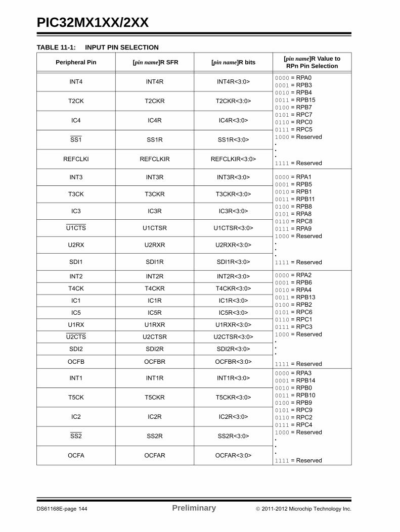
PIC32MX1XX/2XX
TABLE 11-1: INPUT PIN SELECTION
Peripheral Pin [pin name]R SFR [pin name]R bits[pin name]R Value to RPn Pin Selection
INT4 INT4R INT4R<3:0>0000 = RPA00001 = RPB30010 = RPB40011 = RPB150100 = RPB70101 = RPC70110 = RPC00111 = RPC51000 = Reserved•••
1111 = Reserved
T2CK T2CKR T2CKR<3:0>
IC4 IC4R IC4R<3:0>
SS1 SS1R SS1R<3:0>
REFCLKI REFCLKIR REFCLKIR<3:0>
INT3 INT3R INT3R<3:0> 0000 = RPA10001 = RPB50010 = RPB10011 = RPB110100 = RPB80101 = RPA80110 = RPC80111 = RPA91000 = Reserved•••
1111 = Reserved
T3CK T3CKR T3CKR<3:0>
IC3 IC3R IC3R<3:0>
U1CTS U1CTSR U1CTSR<3:0>
U2RX U2RXR U2RXR<3:0>
SDI1 SDI1R SDI1R<3:0>
INT2 INT2R INT2R<3:0> 0000 = RPA20001 = RPB60010 = RPA40011 = RPB130100 = RPB20101 = RPC60110 = RPC10111 = RPC31000 = Reserved•••
1111 = Reserved
T4CK T4CKR T4CKR<3:0>
IC1 IC1R IC1R<3:0>
IC5 IC5R IC5R<3:0>
U1RX U1RXR U1RXR<3:0>
U2CTS U2CTSR U2CTSR<3:0>
SDI2 SDI2R SDI2R<3:0>
OCFB OCFBR OCFBR<3:0>
INT1 INT1R INT1R<3:0>0000 = RPA30001 = RPB140010 = RPB00011 = RPB100100 = RPB90101 = RPC90110 = RPC20111 = RPC41000 = Reserved•
•
•
1111 = Reserved
T5CK T5CKR T5CKR<3:0>
IC2 IC2R IC2R<3:0>
SS2 SS2R SS2R<3:0>
OCFA OCFAR OCFAR<3:0>
DS61168E-page 144 Preliminary 2011-2012 Microchip Technology Inc.
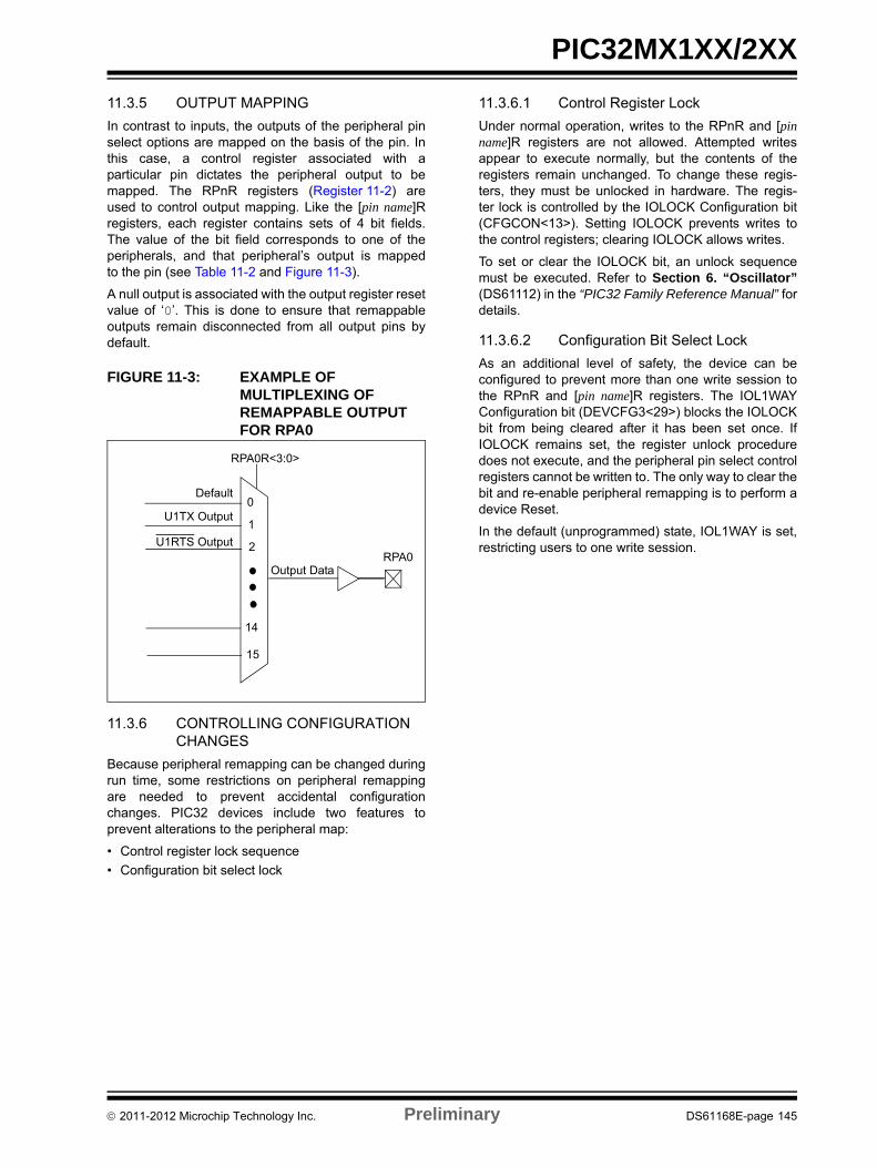
PIC32MX1XX/2XX
11.3.5 OUTPUT MAPPING
In contrast to inputs, the outputs of the peripheral pinselect options are mapped on the basis of the pin. Inthis case, a control register associated with aparticular pin dictates the peripheral output to bemapped. The RPnR registers (Register 11-2) areused to control output mapping. Like the [pin name]Rregisters, each register contains sets of 4 bit fields.The value of the bit field corresponds to one of theperipherals, and that peripheral’s output is mappedto the pin (see Table 11-2 and Figure 11-3).
A null output is associated with the output register resetvalue of ‘0’. This is done to ensure that remappableoutputs remain disconnected from all output pins bydefault.
FIGURE 11-3: EXAMPLE OF MULTIPLEXING OF REMAPPABLE OUTPUT FOR RPA0
11.3.6 CONTROLLING CONFIGURATION CHANGES
Because peripheral remapping can be changed duringrun time, some restrictions on peripheral remappingare needed to prevent accidental configurationchanges. PIC32 devices include two features toprevent alterations to the peripheral map:
• Control register lock sequence
• Configuration bit select lock
11.3.6.1 Control Register Lock
Under normal operation, writes to the RPnR and [pinname]R registers are not allowed. Attempted writesappear to execute normally, but the contents of theregisters remain unchanged. To change these regis-ters, they must be unlocked in hardware. The regis-ter lock is controlled by the IOLOCK Configuration bit(CFGCON<13>). Setting IOLOCK prevents writes tothe control registers; clearing IOLOCK allows writes.
To set or clear the IOLOCK bit, an unlock sequencemust be executed. Refer to Section 6. “Oscillator”(DS61112) in the “PIC32 Family Reference Manual” fordetails.
11.3.6.2 Configuration Bit Select Lock
As an additional level of safety, the device can beconfigured to prevent more than one write session tothe RPnR and [pin name]R registers. The IOL1WAYConfiguration bit (DEVCFG3<29>) blocks the IOLOCKbit from being cleared after it has been set once. IfIOLOCK remains set, the register unlock proceduredoes not execute, and the peripheral pin select controlregisters cannot be written to. The only way to clear thebit and re-enable peripheral remapping is to perform adevice Reset.
In the default (unprogrammed) state, IOL1WAY is set,restricting users to one write session.
RPA0R<3:0>
0
15
1
Default
U1TX Output
U1RTS Output 2
14
Output DataRPA0
2011-2012 Microchip Technology Inc. Preliminary DS61168E-page 145
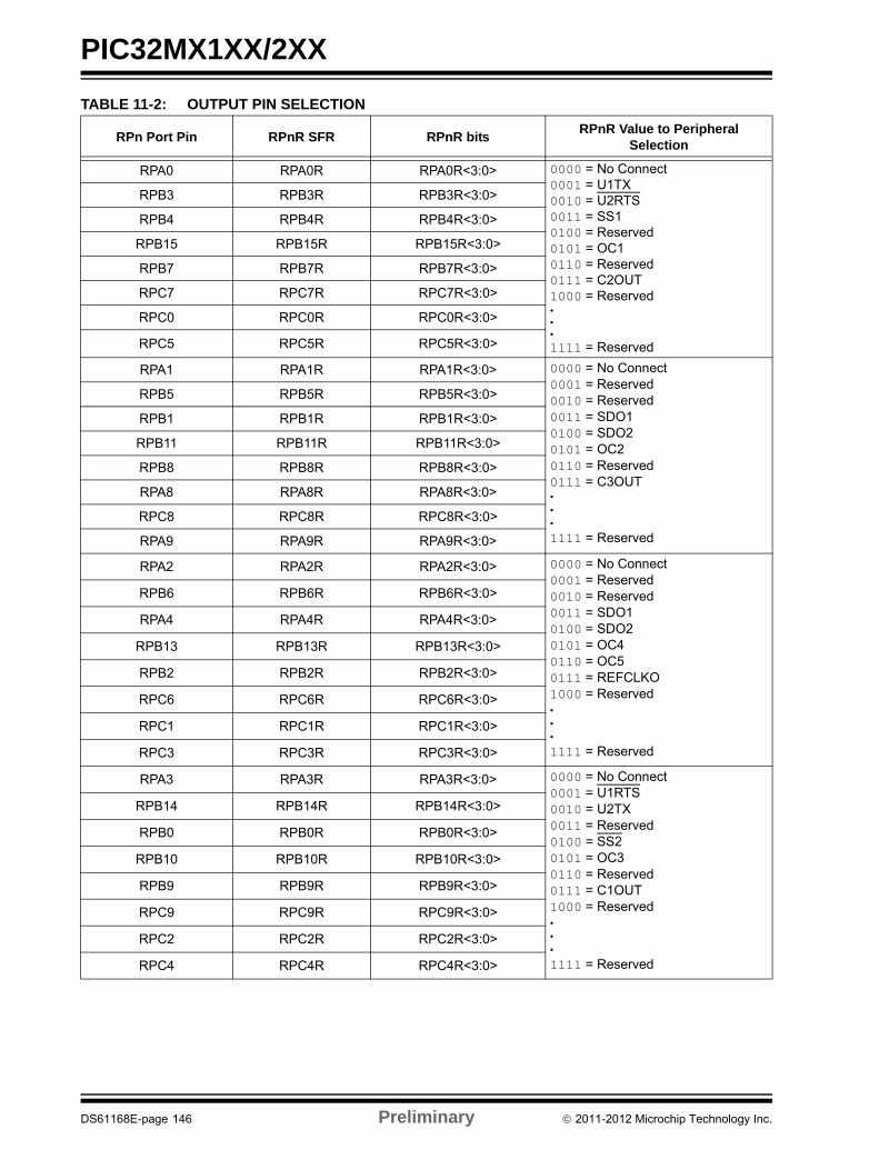
PIC32MX1XX/2XX
TABLE 11-2: OUTPUT PIN SELECTION
RPn Port Pin RPnR SFR RPnR bitsRPnR Value to Peripheral
Selection
RPA0 RPA0R RPA0R<3:0> 0000 = No Connect0001 = U1TX0010 = U2RTS0011 = SS10100 = Reserved0101 = OC10110 = Reserved0111 = C2OUT1000 = Reserved•••1111 = Reserved
RPB3 RPB3R RPB3R<3:0>
RPB4 RPB4R RPB4R<3:0>
RPB15 RPB15R RPB15R<3:0>
RPB7 RPB7R RPB7R<3:0>
RPC7 RPC7R RPC7R<3:0>
RPC0 RPC0R RPC0R<3:0>
RPC5 RPC5R RPC5R<3:0>
RPA1 RPA1R RPA1R<3:0> 0000 = No Connect0001 = Reserved0010 = Reserved0011 = SDO10100 = SDO20101 = OC20110 = Reserved0111 = C3OUT•••
1111 = Reserved
RPB5 RPB5R RPB5R<3:0>
RPB1 RPB1R RPB1R<3:0>
RPB11 RPB11R RPB11R<3:0>
RPB8 RPB8R RPB8R<3:0>
RPA8 RPA8R RPA8R<3:0>
RPC8 RPC8R RPC8R<3:0>
RPA9 RPA9R RPA9R<3:0>
RPA2 RPA2R RPA2R<3:0> 0000 = No Connect0001 = Reserved0010 = Reserved0011 = SDO10100 = SDO20101 = OC40110 = OC50111 = REFCLKO1000 = Reserved•••
1111 = Reserved
RPB6 RPB6R RPB6R<3:0>
RPA4 RPA4R RPA4R<3:0>
RPB13 RPB13R RPB13R<3:0>
RPB2 RPB2R RPB2R<3:0>
RPC6 RPC6R RPC6R<3:0>
RPC1 RPC1R RPC1R<3:0>
RPC3 RPC3R RPC3R<3:0>
RPA3 RPA3R RPA3R<3:0> 0000 = No Connect0001 = U1RTS0010 = U2TX0011 = Reserved0100 = SS20101 = OC30110 = Reserved0111 = C1OUT1000 = Reserved•••
1111 = Reserved
RPB14 RPB14R RPB14R<3:0>
RPB0 RPB0R RPB0R<3:0>
RPB10 RPB10R RPB10R<3:0>
RPB9 RPB9R RPB9R<3:0>
RPC9 RPC9R RPC9R<3:0>
RPC2 RPC2R RPC2R<3:0>
RPC4 RPC4R RPC4R<3:0>
DS61168E-page 146 Preliminary 2011-2012 Microchip Technology Inc.
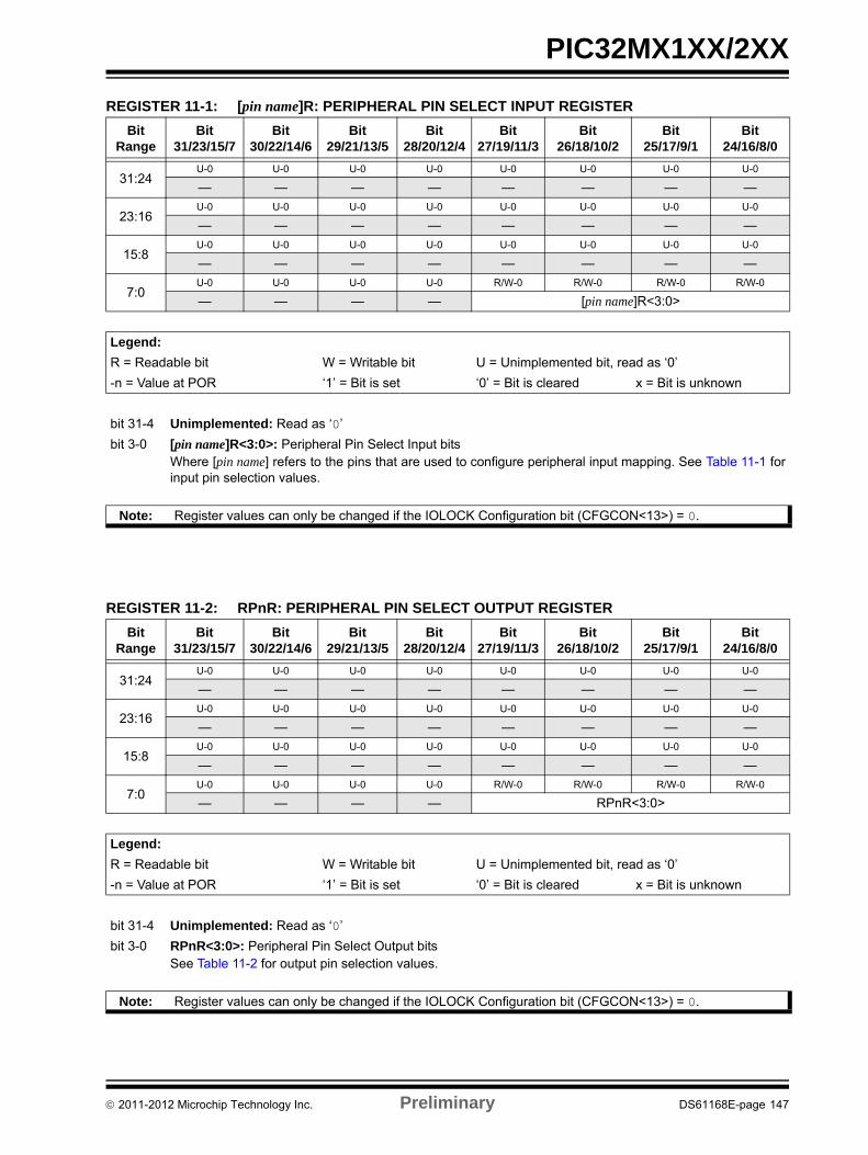
PIC32MX1XX/2XX
REGISTER 11-1: [pin name]R: PERIPHERAL PIN SELECT INPUT REGISTER
Bit Range
Bit31/23/15/7
Bit30/22/14/6
Bit29/21/13/5
Bit28/20/12/4
Bit27/19/11/3
Bit26/18/10/2
Bit25/17/9/1
Bit24/16/8/0
31:24U-0 U-0 U-0 U-0 U-0 U-0 U-0 U-0
— — — — — — — —
23:16U-0 U-0 U-0 U-0 U-0 U-0 U-0 U-0
— — — — — — — —
15:8U-0 U-0 U-0 U-0 U-0 U-0 U-0 U-0
— — — — — — — —
7:0U-0 U-0 U-0 U-0 R/W-0 R/W-0 R/W-0 R/W-0
— — — — [pin name]R<3:0>
Legend:
R = Readable bit W = Writable bit U = Unimplemented bit, read as ‘0’
-n = Value at POR ‘1’ = Bit is set ‘0’ = Bit is cleared x = Bit is unknown
bit 31-4 Unimplemented: Read as ‘0’
bit 3-0 [pin name]R<3:0>: Peripheral Pin Select Input bitsWhere [pin name] refers to the pins that are used to configure peripheral input mapping. See Table 11-1 forinput pin selection values.
Note: Register values can only be changed if the IOLOCK Configuration bit (CFGCON<13>) = 0.
REGISTER 11-2: RPnR: PERIPHERAL PIN SELECT OUTPUT REGISTER
Bit Range
Bit31/23/15/7
Bit30/22/14/6
Bit29/21/13/5
Bit28/20/12/4
Bit27/19/11/3
Bit26/18/10/2
Bit25/17/9/1
Bit24/16/8/0
31:24U-0 U-0 U-0 U-0 U-0 U-0 U-0 U-0
— — — — — — — —
23:16U-0 U-0 U-0 U-0 U-0 U-0 U-0 U-0
— — — — — — — —
15:8U-0 U-0 U-0 U-0 U-0 U-0 U-0 U-0
— — — — — — — —
7:0U-0 U-0 U-0 U-0 R/W-0 R/W-0 R/W-0 R/W-0
— — — — RPnR<3:0>
Legend:
R = Readable bit W = Writable bit U = Unimplemented bit, read as ‘0’
-n = Value at POR ‘1’ = Bit is set ‘0’ = Bit is cleared x = Bit is unknown
bit 31-4 Unimplemented: Read as ‘0’
bit 3-0 RPnR<3:0>: Peripheral Pin Select Output bitsSee Table 11-2 for output pin selection values.
Note: Register values can only be changed if the IOLOCK Configuration bit (CFGCON<13>) = 0.
2011-2012 Microchip Technology Inc. Preliminary DS61168E-page 147
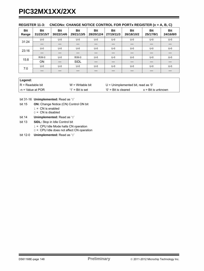
PIC32MX1XX/2XX
REGISTER 11-3: CNCONx: CHANGE NOTICE CONTROL FOR PORTx REGISTER (x = A, B, C)
Bit Range
Bit31/23/15/7
Bit30/22/14/6
Bit29/21/13/5
Bit28/20/12/4
Bit27/19/11/3
Bit26/18/10/2
Bit25/17/9/1
Bit24/16/8/0
31:24U-0 U-0 U-0 U-0 U-0 U-0 U-0 U-0
— — — — — — — —
23:16U-0 U-0 U-0 U-0 U-0 U-0 U-0 U-0
— — — — — — — —
15:8R/W-0 U-0 R/W-0 U-0 U-0 U-0 U-0 U-0
ON — SIDL — — — — —
7:0U-0 U-0 U-0 U-0 U-0 U-0 U-0 U-0
— — — — — — — —
Legend:
R = Readable bit W = Writable bit U = Unimplemented bit, read as ‘0’
-n = Value at POR ‘1’ = Bit is set ‘0’ = Bit is cleared x = Bit is unknown
bit 31-16 Unimplemented: Read as ‘0’
bit 15 ON: Change Notice (CN) Control ON bit
1 = CN is enabled0 = CN is disabled
bit 14 Unimplemented: Read as ‘0’
bit 13 SIDL: Stop in Idle Control bit
1 = CPU Idle Mode halts CN operation0 = CPU Idle does not affect CN operation
bit 12-0 Unimplemented: Read as ‘0’
DS61168E-page 148 Preliminary 2011-2012 Microchip Technology Inc.
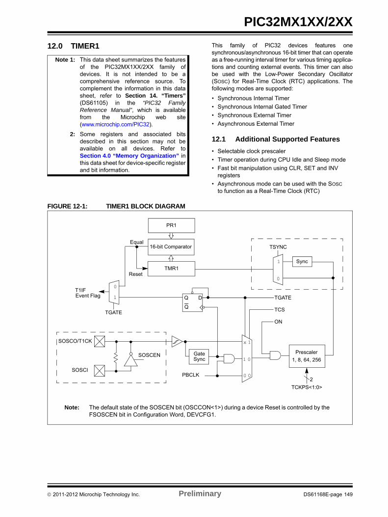
PIC32MX1XX/2XX
12.0 TIMER1 This family of PIC32 devices features onesynchronous/asynchronous 16-bit timer that can operateas a free-running interval timer for various timing applica-tions and counting external events. This timer can alsobe used with the Low-Power Secondary Oscillator(SOSC) for Real-Time Clock (RTC) applications. Thefollowing modes are supported:
• Synchronous Internal Timer
• Synchronous Internal Gated Timer
• Synchronous External Timer
• Asynchronous External Timer
12.1 Additional Supported Features
• Selectable clock prescaler
• Timer operation during CPU Idle and Sleep mode
• Fast bit manipulation using CLR, SET and INV registers
• Asynchronous mode can be used with the SOSC to function as a Real-Time Clock (RTC)
FIGURE 12-1: TIMER1 BLOCK DIAGRAM
Note 1: This data sheet summarizes the featuresof the PIC32MX1XX/2XX family ofdevices. It is not intended to be acomprehensive reference source. Tocomplement the information in this datasheet, refer to Section 14. “Timers”(DS61105) in the “PIC32 FamilyReference Manual”, which is availablefrom the Microchip web site(www.microchip.com/PIC32).
2: Some registers and associated bitsdescribed in this section may not beavailable on all devices. Refer toSection 4.0 “Memory Organization” inthis data sheet for device-specific registerand bit information.
ON
Sync
SOSCI
SOSCO/T1CK
PR1
T1IF
Equal16-bit Comparator
TMR1Reset
SOSCEN
Event Flag
1
0
TSYNC
TGATE
TGATE
PBCLK
1
0
TCS
GateSync
TCKPS<1:0>
Prescaler
2
1, 8, 64, 256
x 1
1 0
0 0
Q
Q D
Note: The default state of the SOSCEN bit (OSCCON<1>) during a device Reset is controlled by theFSOSCEN bit in Configuration Word, DEVCFG1.
2011-2012 Microchip Technology Inc. Preliminary DS61168E-page 149
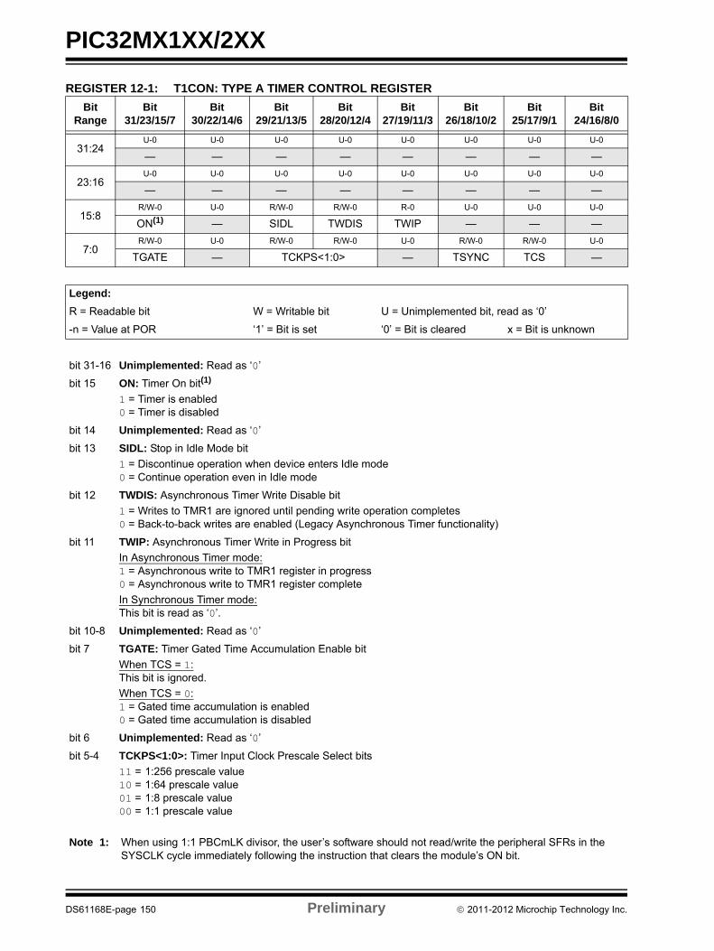
PIC32MX1XX/2XX
REGISTER 12-1: T1CON: TYPE A TIMER CONTROL REGISTER
Bit Range
Bit31/23/15/7
Bit30/22/14/6
Bit29/21/13/5
Bit28/20/12/4
Bit27/19/11/3
Bit26/18/10/2
Bit25/17/9/1
Bit24/16/8/0
31:24U-0 U-0 U-0 U-0 U-0 U-0 U-0 U-0
— — — — — — — —
23:16U-0 U-0 U-0 U-0 U-0 U-0 U-0 U-0
— — — — — — — —
15:8R/W-0 U-0 R/W-0 R/W-0 R-0 U-0 U-0 U-0
ON(1) — SIDL TWDIS TWIP — — —
7:0R/W-0 U-0 R/W-0 R/W-0 U-0 R/W-0 R/W-0 U-0
TGATE — TCKPS<1:0> — TSYNC TCS —
Legend:
R = Readable bit W = Writable bit U = Unimplemented bit, read as ‘0’
-n = Value at POR ‘1’ = Bit is set ‘0’ = Bit is cleared x = Bit is unknown
bit 31-16 Unimplemented: Read as ‘0’
bit 15 ON: Timer On bit(1)
1 = Timer is enabled0 = Timer is disabled
bit 14 Unimplemented: Read as ‘0’
bit 13 SIDL: Stop in Idle Mode bit
1 = Discontinue operation when device enters Idle mode0 = Continue operation even in Idle mode
bit 12 TWDIS: Asynchronous Timer Write Disable bit
1 = Writes to TMR1 are ignored until pending write operation completes0 = Back-to-back writes are enabled (Legacy Asynchronous Timer functionality)
bit 11 TWIP: Asynchronous Timer Write in Progress bit
In Asynchronous Timer mode:1 = Asynchronous write to TMR1 register in progress0 = Asynchronous write to TMR1 register complete
In Synchronous Timer mode:This bit is read as ‘0’.
bit 10-8 Unimplemented: Read as ‘0’
bit 7 TGATE: Timer Gated Time Accumulation Enable bit
When TCS = 1:This bit is ignored.
When TCS = 0:1 = Gated time accumulation is enabled0 = Gated time accumulation is disabled
bit 6 Unimplemented: Read as ‘0’
bit 5-4 TCKPS<1:0>: Timer Input Clock Prescale Select bits
11 = 1:256 prescale value10 = 1:64 prescale value01 = 1:8 prescale value00 = 1:1 prescale value
Note 1: When using 1:1 PBCmLK divisor, the user’s software should not read/write the peripheral SFRs in the SYSCLK cycle immediately following the instruction that clears the module’s ON bit.
DS61168E-page 150 Preliminary 2011-2012 Microchip Technology Inc.
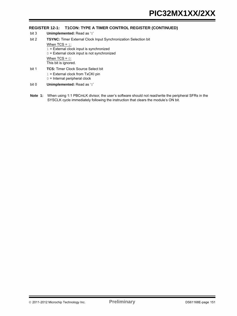
PIC32MX1XX/2XX
bit 3 Unimplemented: Read as ‘0’
bit 2 TSYNC: Timer External Clock Input Synchronization Selection bit
When TCS = 1:1 = External clock input is synchronized0 = External clock input is not synchronized
When TCS = 0:This bit is ignored.
bit 1 TCS: Timer Clock Source Select bit
1 = External clock from TxCKI pin0 = Internal peripheral clock
bit 0 Unimplemented: Read as ‘0’
REGISTER 12-1: T1CON: TYPE A TIMER CONTROL REGISTER (CONTINUED)
Note 1: When using 1:1 PBCmLK divisor, the user’s software should not read/write the peripheral SFRs in the SYSCLK cycle immediately following the instruction that clears the module’s ON bit.
2011-2012 Microchip Technology Inc. Preliminary DS61168E-page 151

PIC32MX1XX/2XX
NOTES:
DS61168E-page 152 Preliminary 2011-2012 Microchip Technology Inc.
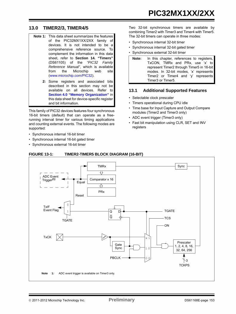
PIC32MX1XX/2XX
13.0 TIMER2/3, TIMER4/5
This family of PIC32 devices features four synchronous16-bit timers (default) that can operate as a free-running interval timer for various timing applicationsand counting external events. The following modes aresupported:
• Synchronous internal 16-bit timer
• Synchronous internal 16-bit gated timer
• Synchronous external 16-bit timer
Two 32-bit synchronous timers are available bycombining Timer2 with Timer3 and Timer4 with Timer5.The 32-bit timers can operate in three modes:
• Synchronous internal 32-bit timer
• Synchronous internal 32-bit gated timer
• Synchronous external 32-bit timer
13.1 Additional Supported Features
• Selectable clock prescaler
• Timers operational during CPU idle
• Time base for Input Capture and Output Compare modules (Timer2 and Timer3 only)
• ADC event trigger (Timer3 only)
• Fast bit manipulation using CLR, SET and INV registers
FIGURE 13-1: TIMER2-TIMER5 BLOCK DIAGRAM (16-BIT)
Note 1: This data sheet summarizes the featuresof the PIC32MX1XX/2XX family ofdevices. It is not intended to be acomprehensive reference source. Tocomplement the information in this datasheet, refer to Section 14. “Timers”(DS61105) of the “PIC32 FamilyReference Manual”, which is availablefrom the Microchip web site(www.microchip.com/PIC32).
2: Some registers and associated bitsdescribed in this section may not beavailable on all devices. Refer toSection 4.0 “Memory Organization” inthis data sheet for device-specific registerand bit information.
Note: In this chapter, references to registers,TxCON, TMRx and PRx, use ‘x’ torepresent Timer2 through Timer5 in 16-bitmodes. In 32-bit modes, ‘x’ representsTimer2 or Timer4 and ‘y’ representsTimer3 or Timer5.
Sync
PRx
TxIF
EqualComparator x 16
TMRx
Reset
Event Flag
Q
Q D
TGATE
1
0
Gate
TxCK
Sync
ON
TGATE
TCS
TCKPS
Prescaler
3
1, 2, 4, 8, 16,32, 64, 256
x 1
1 0
0 0PBCLK
Trigger(1)ADC Event
Note 1: ADC event trigger is available on Timer3 only.
2011-2012 Microchip Technology Inc. Preliminary DS61168E-page 153
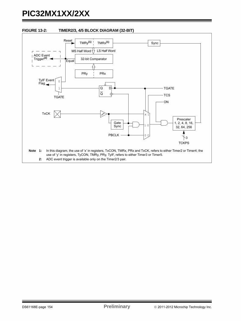
PIC32MX1XX/2XX
FIGURE 13-2: TIMER2/3, 4/5 BLOCK DIAGRAM (32-BIT)
TMRy(1) TMRx(1)
TyIF Event
Equal 32-bit Comparator
PRy PRx
Reset
LS Half WordMS Half Word
Flag
Note 1: In this diagram, the use of ‘x’ in registers, TxCON, TMRx, PRx and TxCK, refers to either Timer2 or Timer4; the use of ‘y’ in registers, TyCON, TMRy, PRy, TyIF, refers to either Timer3 or Timer5.
2: ADC event trigger is available only on the Timer2/3 pair.
TGATE
0
1
PBCLK
Gate
TxCK
Sync
Sync
ADC EventTrigger(2)
ON
TGATE
TCS
TCKPS
Prescaler
3
1, 2, 4, 8, 16,32, 64, 256
1 0
0 0
Q
Q D
x 1
DS61168E-page 154 Preliminary 2011-2012 Microchip Technology Inc.
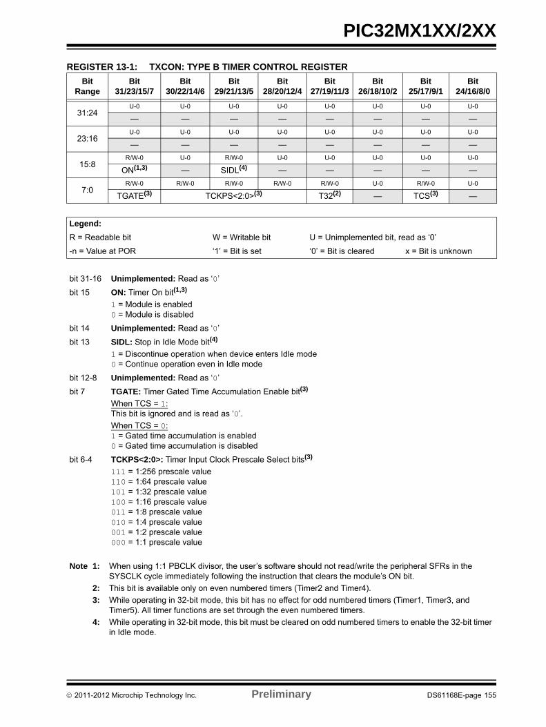
PIC32MX1XX/2XX
REGISTER 13-1: TXCON: TYPE B TIMER CONTROL REGISTER
Bit Range
Bit31/23/15/7
Bit30/22/14/6
Bit29/21/13/5
Bit28/20/12/4
Bit27/19/11/3
Bit26/18/10/2
Bit25/17/9/1
Bit24/16/8/0
31:24U-0 U-0 U-0 U-0 U-0 U-0 U-0 U-0
— — — — — — — —
23:16U-0 U-0 U-0 U-0 U-0 U-0 U-0 U-0
— — — — — — — —
15:8R/W-0 U-0 R/W-0 U-0 U-0 U-0 U-0 U-0
ON(1,3) — SIDL(4) — — — — —
7:0R/W-0 R/W-0 R/W-0 R/W-0 R/W-0 U-0 R/W-0 U-0
TGATE(3) TCKPS<2:0>(3) T32(2) — TCS(3) —
Legend:
R = Readable bit W = Writable bit U = Unimplemented bit, read as ‘0’
-n = Value at POR ‘1’ = Bit is set ‘0’ = Bit is cleared x = Bit is unknown
bit 31-16 Unimplemented: Read as ‘0’
bit 15 ON: Timer On bit(1,3)
1 = Module is enabled0 = Module is disabled
bit 14 Unimplemented: Read as ‘0’
bit 13 SIDL: Stop in Idle Mode bit(4)
1 = Discontinue operation when device enters Idle mode0 = Continue operation even in Idle mode
bit 12-8 Unimplemented: Read as ‘0’
bit 7 TGATE: Timer Gated Time Accumulation Enable bit(3)
When TCS = 1:This bit is ignored and is read as ‘0’.
When TCS = 0:1 = Gated time accumulation is enabled0 = Gated time accumulation is disabled
bit 6-4 TCKPS<2:0>: Timer Input Clock Prescale Select bits(3)
111 = 1:256 prescale value110 = 1:64 prescale value101 = 1:32 prescale value100 = 1:16 prescale value011 = 1:8 prescale value010 = 1:4 prescale value001 = 1:2 prescale value000 = 1:1 prescale value
Note 1: When using 1:1 PBCLK divisor, the user’s software should not read/write the peripheral SFRs in the SYSCLK cycle immediately following the instruction that clears the module’s ON bit.
2: This bit is available only on even numbered timers (Timer2 and Timer4).
3: While operating in 32-bit mode, this bit has no effect for odd numbered timers (Timer1, Timer3, and Timer5). All timer functions are set through the even numbered timers.
4: While operating in 32-bit mode, this bit must be cleared on odd numbered timers to enable the 32-bit timer in Idle mode.
2011-2012 Microchip Technology Inc. Preliminary DS61168E-page 155
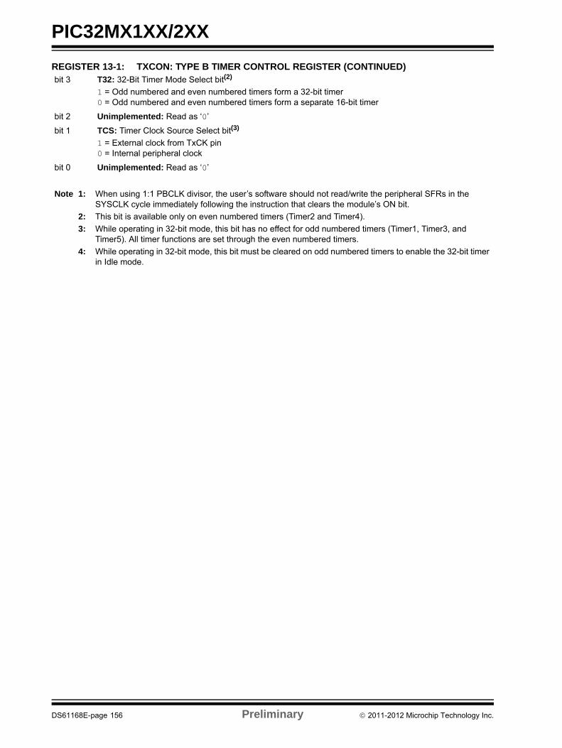
PIC32MX1XX/2XX
bit 3 T32: 32-Bit Timer Mode Select bit(2)
1 = Odd numbered and even numbered timers form a 32-bit timer0 = Odd numbered and even numbered timers form a separate 16-bit timer
bit 2 Unimplemented: Read as ‘0’
bit 1 TCS: Timer Clock Source Select bit(3)
1 = External clock from TxCK pin0 = Internal peripheral clock
bit 0 Unimplemented: Read as ‘0’
REGISTER 13-1: TXCON: TYPE B TIMER CONTROL REGISTER (CONTINUED)
Note 1: When using 1:1 PBCLK divisor, the user’s software should not read/write the peripheral SFRs in the SYSCLK cycle immediately following the instruction that clears the module’s ON bit.
2: This bit is available only on even numbered timers (Timer2 and Timer4).
3: While operating in 32-bit mode, this bit has no effect for odd numbered timers (Timer1, Timer3, and Timer5). All timer functions are set through the even numbered timers.
4: While operating in 32-bit mode, this bit must be cleared on odd numbered timers to enable the 32-bit timer in Idle mode.
DS61168E-page 156 Preliminary 2011-2012 Microchip Technology Inc.
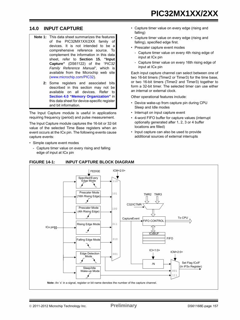
PIC32MX1XX/2XX
14.0 INPUT CAPTURE
The Input Capture module is useful in applicationsrequiring frequency (period) and pulse measurement.
The Input Capture module captures the 16-bit or 32-bitvalue of the selected Time Base registers when anevent occurs at the ICx pin. The following events causecapture events:
• Simple capture event modes
- Capture timer value on every rising and falling edge of input at ICx pin
• Capture timer value on every edge (rising and falling)
• Capture timer value on every edge (rising and falling), specified edge first.
• Prescaler capture event modes
- Capture timer value on every 4th rising edge of input at ICx pin
- Capture timer value on every 16th rising edge of input at ICx pin
Each input capture channel can select between one oftwo 16-bit timers (Timer2 or Timer3) for the time base,or two 16-bit timers (Timer2 and Timer3) together toform a 32-bit timer. The selected timer can use eitheran internal or external clock.
Other operational features include:
• Device wake-up from capture pin during CPU Sleep and Idle modes
• Interrupt on input capture event
• 4-word FIFO buffer for capture values (interrupt optionally generated after 1, 2, 3 or 4 buffer locations are filled)
• Input capture can also be used to provide additional sources of external interrupts
FIGURE 14-1: INPUT CAPTURE BLOCK DIAGRAM
Note 1: This data sheet summarizes the featuresof the PIC32MX1XX/2XX family ofdevices. It is not intended to be acomprehensive reference source. Tocomplement the information in this datasheet, refer to Section 15. “InputCapture” (DS61122) of the “PIC32Family Reference Manual”, which isavailable from the Microchip web site(www.microchip.com/PIC32).
2: Some registers and associated bitsdescribed in this section may not beavailable on all devices. Refer toSection 4.0 “Memory Organization” inthis data sheet for device-specific registerand bit information.
Note: An ‘x’ in a signal, register or bit name denotes the number of the capture channel.
FIFO CONTROL
ICxBUF
TMR2 TMR3
CaptureEvent
/N
FIFO
ICI<1:0>
ICM<2:0>
ICM<2:0>
101
100
011
010
001
001
111
To CPU
Set Flag ICxIF(In IFSx Register)
Rising Edge Mode
Prescaler Mode (4th Rising Edge)
Falling Edge Mode
Edge Detection
Prescaler Mode (16th Rising Edge)
Sleep/IdleWake-up Mode
C32/ICTMR
ICx pin
Mode
110Specified/Every
Edge Mode
FEDGE
2011-2012 Microchip Technology Inc. Preliminary DS61168E-page 157
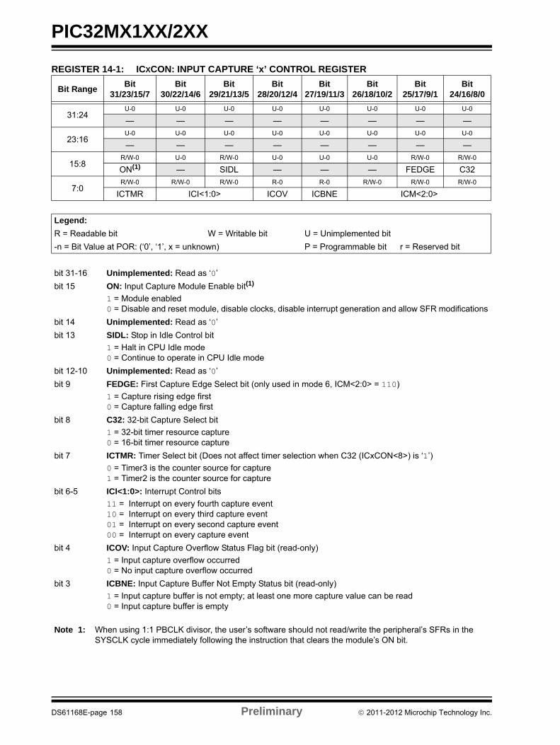
PIC32MX1XX/2XX
REGISTER 14-1: ICXCON: INPUT CAPTURE ‘x’ CONTROL REGISTER
Bit RangeBit
31/23/15/7Bit
30/22/14/6Bit
29/21/13/5Bit
28/20/12/4Bit
27/19/11/3Bit
26/18/10/2Bit
25/17/9/1Bit
24/16/8/0
31:24U-0 U-0 U-0 U-0 U-0 U-0 U-0 U-0
— — — — — — — —
23:16U-0 U-0 U-0 U-0 U-0 U-0 U-0 U-0
— — — — — — — —
15:8R/W-0 U-0 R/W-0 U-0 U-0 U-0 R/W-0 R/W-0
ON(1) — SIDL — — — FEDGE C32
7:0R/W-0 R/W-0 R/W-0 R-0 R-0 R/W-0 R/W-0 R/W-0
ICTMR ICI<1:0> ICOV ICBNE ICM<2:0>
Legend:
R = Readable bit W = Writable bit U = Unimplemented bit
-n = Bit Value at POR: (‘0’, ‘1’, x = unknown) P = Programmable bit r = Reserved bit
bit 31-16 Unimplemented: Read as ‘0’
bit 15 ON: Input Capture Module Enable bit(1)
1 = Module enabled0 = Disable and reset module, disable clocks, disable interrupt generation and allow SFR modifications
bit 14 Unimplemented: Read as ‘0’
bit 13 SIDL: Stop in Idle Control bit
1 = Halt in CPU Idle mode0 = Continue to operate in CPU Idle mode
bit 12-10 Unimplemented: Read as ‘0’
bit 9 FEDGE: First Capture Edge Select bit (only used in mode 6, ICM<2:0> = 110)
1 = Capture rising edge first0 = Capture falling edge first
bit 8 C32: 32-bit Capture Select bit
1 = 32-bit timer resource capture0 = 16-bit timer resource capture
bit 7 ICTMR: Timer Select bit (Does not affect timer selection when C32 (ICxCON<8>) is ‘1’)
0 = Timer3 is the counter source for capture1 = Timer2 is the counter source for capture
bit 6-5 ICI<1:0>: Interrupt Control bits
11 = Interrupt on every fourth capture event10 = Interrupt on every third capture event01 = Interrupt on every second capture event00 = Interrupt on every capture event
bit 4 ICOV: Input Capture Overflow Status Flag bit (read-only)
1 = Input capture overflow occurred0 = No input capture overflow occurred
bit 3 ICBNE: Input Capture Buffer Not Empty Status bit (read-only)
1 = Input capture buffer is not empty; at least one more capture value can be read0 = Input capture buffer is empty
Note 1: When using 1:1 PBCLK divisor, the user’s software should not read/write the peripheral’s SFRs in the SYSCLK cycle immediately following the instruction that clears the module’s ON bit.
DS61168E-page 158 Preliminary 2011-2012 Microchip Technology Inc.
PIC32MX1XX/2XX
bit 2-0 ICM<2:0>: Input Capture Mode Select bits
111 = Interrupt-Only mode (only supported while in Sleep mode or Idle mode)110 = Simple Capture Event mode – every edge, specified edge first and every edge thereafter101 = Prescaled Capture Event mode – every sixteenth rising edge100 = Prescaled Capture Event mode – every fourth rising edge011 = Simple Capture Event mode – every rising edge010 = Simple Capture Event mode – every falling edge001 = Edge Detect mode – every edge (rising and falling)000 = Input Capture module is disabled
REGISTER 14-1: ICXCON: INPUT CAPTURE ‘x’ CONTROL REGISTER (CONTINUED)
Note 1: When using 1:1 PBCLK divisor, the user’s software should not read/write the peripheral’s SFRs in the SYSCLK cycle immediately following the instruction that clears the module’s ON bit.
2011-2012 Microchip Technology Inc. Preliminary DS61168E-page 159

PIC32MX1XX/2XX
NOTES:
DS61168E-page 160 Preliminary 2011-2012 Microchip Technology Inc.
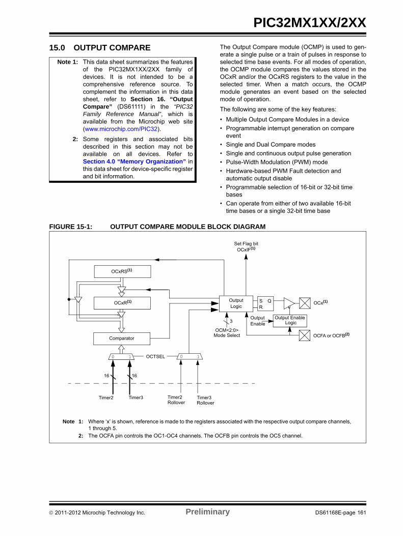
PIC32MX1XX/2XX
15.0 OUTPUT COMPARE The Output Compare module (OCMP) is used to gen-erate a single pulse or a train of pulses in response toselected time base events. For all modes of operation,the OCMP module compares the values stored in theOCxR and/or the OCxRS registers to the value in theselected timer. When a match occurs, the OCMPmodule generates an event based on the selectedmode of operation.
The following are some of the key features:
• Multiple Output Compare Modules in a device
• Programmable interrupt generation on compare event
• Single and Dual Compare modes
• Single and continuous output pulse generation
• Pulse-Width Modulation (PWM) mode
• Hardware-based PWM Fault detection and automatic output disable
• Programmable selection of 16-bit or 32-bit time bases
• Can operate from either of two available 16-bit time bases or a single 32-bit time base
FIGURE 15-1: OUTPUT COMPARE MODULE BLOCK DIAGRAM
Note 1: This data sheet summarizes the featuresof the PIC32MX1XX/2XX family ofdevices. It is not intended to be acomprehensive reference source. Tocomplement the information in this datasheet, refer to Section 16. “OutputCompare” (DS61111) in the “PIC32Family Reference Manual”, which isavailable from the Microchip web site(www.microchip.com/PIC32).
2: Some registers and associated bitsdescribed in this section may not beavailable on all devices. Refer toSection 4.0 “Memory Organization” inthis data sheet for device-specific registerand bit information.
OCxR(1)
Comparator
OutputLogic
QSR
OCM<2:0>
Output Enable
OCx(1)
Set Flag bitOCxIF(1)
OCxRS(1)
Mode Select
3
Note 1: Where ‘x’ is shown, reference is made to the registers associated with the respective output compare channels,1 through 5.
2: The OCFA pin controls the OC1-OC4 channels. The OCFB pin controls the OC5 channel.
0 1 OCTSEL 0 1
16 16
OCFA or OCFB(2)
Timer2 Timer2 Timer3
LogicOutput Enable
Timer3Rollover Rollover
2011-2012 Microchip Technology Inc. Preliminary DS61168E-page 161
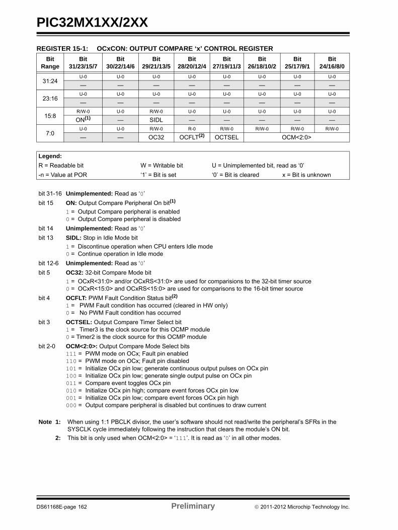
PIC32MX1XX/2XX
REGISTER 15-1: OCxCON: OUTPUT COMPARE ‘x’ CONTROL REGISTER
Bit Range
Bit31/23/15/7
Bit30/22/14/6
Bit29/21/13/5
Bit28/20/12/4
Bit27/19/11/3
Bit26/18/10/2
Bit25/17/9/1
Bit24/16/8/0
31:24U-0 U-0 U-0 U-0 U-0 U-0 U-0 U-0
— — — — — — — —
23:16U-0 U-0 U-0 U-0 U-0 U-0 U-0 U-0
— — — — — — — —
15:8R/W-0 U-0 R/W-0 U-0 U-0 U-0 U-0 U-0
ON(1) — SIDL — — — — —
7:0U-0 U-0 R/W-0 R-0 R/W-0 R/W-0 R/W-0 R/W-0
— — OC32 OCFLT(2) OCTSEL OCM<2:0>
Legend:
R = Readable bit W = Writable bit U = Unimplemented bit, read as ‘0’
-n = Value at POR ‘1’ = Bit is set ‘0’ = Bit is cleared x = Bit is unknown
bit 31-16 Unimplemented: Read as ‘0’
bit 15 ON: Output Compare Peripheral On bit(1)
1 = Output Compare peripheral is enabled0 = Output Compare peripheral is disabled
bit 14 Unimplemented: Read as ‘0’
bit 13 SIDL: Stop in Idle Mode bit
1 = Discontinue operation when CPU enters Idle mode0 = Continue operation in Idle mode
bit 12-6 Unimplemented: Read as ‘0’
bit 5 OC32: 32-bit Compare Mode bit
1 = OCxR<31:0> and/or OCxRS<31:0> are used for comparisions to the 32-bit timer source0 = OCxR<15:0> and OCxRS<15:0> are used for comparisons to the 16-bit timer source
bit 4 OCFLT: PWM Fault Condition Status bit(2)
1 = PWM Fault condition has occurred (cleared in HW only)0 = No PWM Fault condition has occurred
bit 3 OCTSEL: Output Compare Timer Select bit1 = Timer3 is the clock source for this OCMP module0 = Timer2 is the clock source for this OCMP module
bit 2-0 OCM<2:0>: Output Compare Mode Select bits111 = PWM mode on OCx; Fault pin enabled110 = PWM mode on OCx; Fault pin disabled101 = Initialize OCx pin low; generate continuous output pulses on OCx pin100 = Initialize OCx pin low; generate single output pulse on OCx pin011 = Compare event toggles OCx pin010 = Initialize OCx pin high; compare event forces OCx pin low001 = Initialize OCx pin low; compare event forces OCx pin high000 = Output compare peripheral is disabled but continues to draw current
Note 1: When using 1:1 PBCLK divisor, the user’s software should not read/write the peripheral’s SFRs in the SYSCLK cycle immediately following the instruction that clears the module’s ON bit.
2: This bit is only used when OCM<2:0> = ‘111’. It is read as ‘0’ in all other modes.
DS61168E-page 162 Preliminary 2011-2012 Microchip Technology Inc.
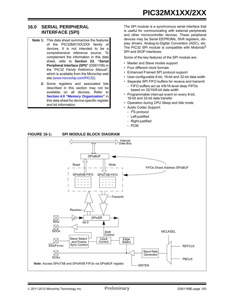
PIC32MX1XX/2XX
16.0 SERIAL PERIPHERAL INTERFACE (SPI)
The SPI module is a synchronous serial interface thatis useful for communicating with external peripheralsand other microcontroller devices. These peripheraldevices may be Serial EEPROMs, Shift registers, dis-play drivers, Analog-to-Digital Converters (ADC), etc.The PIC32 SPI module is compatible with Motorola®
SPI and SIOP interfaces.
Some of the key features of the SPI module are:
• Master and Slave modes support• Four different clock formats• Enhanced Framed SPI protocol support• User-configurable 8-bit, 16-bit and 32-bit data width• Separate SPI FIFO buffers for receive and transmit
- FIFO buffers act as 4/8/16-level deep FIFOs based on 32/16/8-bit data width
• Programmable interrupt event on every 8-bit, 16-bit and 32-bit data transfer
• Operation during CPU Sleep and Idle mode• Audio Codec Support:
- I2S protocol- Left-justified- Right-justified- PCM
FIGURE 16-1: SPI MODULE BLOCK DIAGRAM
Note 1: This data sheet summarizes the featuresof the PIC32MX1XX/2XX family ofdevices. It is not intended to be acomprehensive reference source. Tocomplement the information in this datasheet, refer to Section 23. “SerialPeripheral Interface (SPI)” (DS61106) inthe “PIC32 Family Reference Manual”,which is available from the Microchip website (www.microchip.com/PIC32).
2: Some registers and associated bitsdescribed in this section may not beavailable on all devices. Refer toSection 4.0 “Memory Organization” inthis data sheet for device-specific registerand bit information.
InternalData Bus
SDIx
SDOx
SSx/FSYNC
SCKx
SPIxSR
bit 0
ShiftControl
EdgeSelect
MSTEN
Baud Rate
Slave Select
Sync Control
ClockControl
Transmit
Receive
and Frame
Note: Access SPIxTXB and SPIxRXB FIFOs via SPIxBUF register.
FIFOs Share Address SPIxBUF
SPIxBUF
Generator
PBCLK
WriteRead
SPIxTXB FIFOSPIxRXB FIFO
REFCLK
MCLKSEL
2011-2012 Microchip Technology Inc. Preliminary DS61168E-page 163
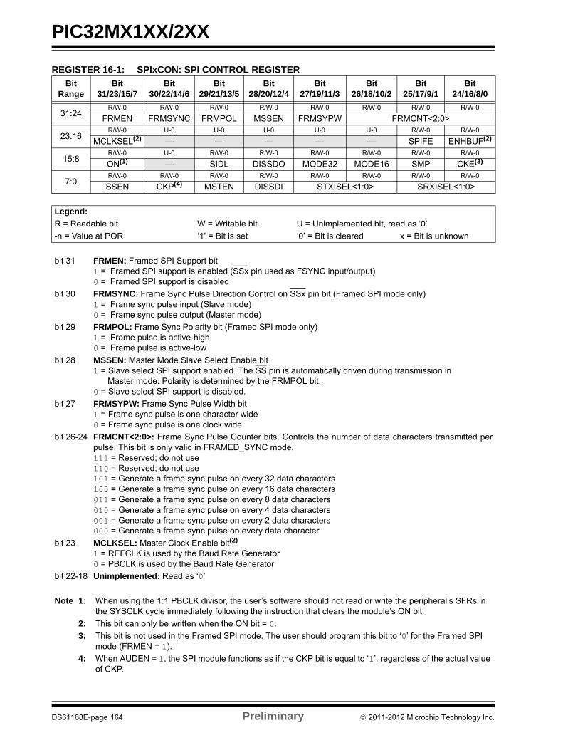
PIC32MX1XX/2XX
REGISTER 16-1: SPIxCON: SPI CONTROL REGISTER
Bit Range
Bit31/23/15/7
Bit30/22/14/6
Bit29/21/13/5
Bit28/20/12/4
Bit27/19/11/3
Bit26/18/10/2
Bit25/17/9/1
Bit24/16/8/0
31:24R/W-0 R/W-0 R/W-0 R/W-0 R/W-0 R/W-0 R/W-0 R/W-0
FRMEN FRMSYNC FRMPOL MSSEN FRMSYPW FRMCNT<2:0>
23:16R/W-0 U-0 U-0 U-0 U-0 U-0 R/W-0 R/W-0
MCLKSEL(2) — — — — — SPIFE ENHBUF(2)
15:8R/W-0 U-0 R/W-0 R/W-0 R/W-0 R/W-0 R/W-0 R/W-0
ON(1) — SIDL DISSDO MODE32 MODE16 SMP CKE(3)
7:0R/W-0 R/W-0 R/W-0 R/W-0 R/W-0 R/W-0 R/W-0 R/W-0
SSEN CKP(4) MSTEN DISSDI STXISEL<1:0> SRXISEL<1:0>
Legend:
R = Readable bit W = Writable bit U = Unimplemented bit, read as ‘0’
-n = Value at POR ‘1’ = Bit is set ‘0’ = Bit is cleared x = Bit is unknown
bit 31 FRMEN: Framed SPI Support bit1 = Framed SPI support is enabled (SSx pin used as FSYNC input/output)0 = Framed SPI support is disabled
bit 30 FRMSYNC: Frame Sync Pulse Direction Control on SSx pin bit (Framed SPI mode only)1 = Frame sync pulse input (Slave mode)0 = Frame sync pulse output (Master mode)
bit 29 FRMPOL: Frame Sync Polarity bit (Framed SPI mode only)1 = Frame pulse is active-high0 = Frame pulse is active-low
bit 28 MSSEN: Master Mode Slave Select Enable bit1 = Slave select SPI support enabled. The SS pin is automatically driven during transmission in
Master mode. Polarity is determined by the FRMPOL bit.0 = Slave select SPI support is disabled.
bit 27 FRMSYPW: Frame Sync Pulse Width bit1 = Frame sync pulse is one character wide0 = Frame sync pulse is one clock wide
bit 26-24 FRMCNT<2:0>: Frame Sync Pulse Counter bits. Controls the number of data characters transmitted perpulse. This bit is only valid in FRAMED_SYNC mode.111 = Reserved; do not use110 = Reserved; do not use101 = Generate a frame sync pulse on every 32 data characters100 = Generate a frame sync pulse on every 16 data characters011 = Generate a frame sync pulse on every 8 data characters010 = Generate a frame sync pulse on every 4 data characters001 = Generate a frame sync pulse on every 2 data characters000 = Generate a frame sync pulse on every data character
bit 23 MCLKSEL: Master Clock Enable bit(2)
1 = REFCLK is used by the Baud Rate Generator0 = PBCLK is used by the Baud Rate Generator
bit 22-18 Unimplemented: Read as ‘0’
Note 1: When using the 1:1 PBCLK divisor, the user’s software should not read or write the peripheral’s SFRs in the SYSCLK cycle immediately following the instruction that clears the module’s ON bit.
2: This bit can only be written when the ON bit = 0.
3: This bit is not used in the Framed SPI mode. The user should program this bit to ‘0’ for the Framed SPI mode (FRMEN = 1).
4: When AUDEN = 1, the SPI module functions as if the CKP bit is equal to ‘1’, regardless of the actual value of CKP.
DS61168E-page 164 Preliminary 2011-2012 Microchip Technology Inc.
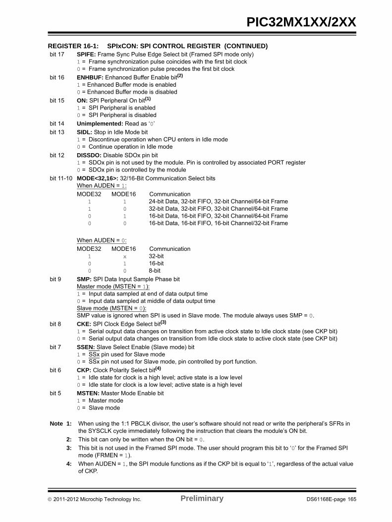
PIC32MX1XX/2XX
bit 17 SPIFE: Frame Sync Pulse Edge Select bit (Framed SPI mode only)1 = Frame synchronization pulse coincides with the first bit clock0 = Frame synchronization pulse precedes the first bit clock
bit 16 ENHBUF: Enhanced Buffer Enable bit(2)
1 = Enhanced Buffer mode is enabled0 = Enhanced Buffer mode is disabled
bit 15 ON: SPI Peripheral On bit(1)
1 = SPI Peripheral is enabled0 = SPI Peripheral is disabled
bit 14 Unimplemented: Read as ‘0’
bit 13 SIDL: Stop in Idle Mode bit1 = Discontinue operation when CPU enters in Idle mode0 = Continue operation in Idle mode
bit 12 DISSDO: Disable SDOx pin bit1 = SDOx pin is not used by the module. Pin is controlled by associated PORT register0 = SDOx pin is controlled by the module
bit 11-10 MODE<32,16>: 32/16-Bit Communication Select bitsWhen AUDEN = 1:
MODE32 MODE16 Communication1 1 24-bit Data, 32-bit FIFO, 32-bit Channel/64-bit Frame1 0 32-bit Data, 32-bit FIFO, 32-bit Channel/64-bit Frame0 1 16-bit Data, 16-bit FIFO, 32-bit Channel/64-bit Frame0 0 16-bit Data, 16-bit FIFO, 16-bit Channel/32-bit Frame
When AUDEN = 0:
MODE32 MODE16 Communication1 x 32-bit0 1 16-bit0 0 8-bit
bit 9 SMP: SPI Data Input Sample Phase bitMaster mode (MSTEN = 1):1 = Input data sampled at end of data output time0 = Input data sampled at middle of data output timeSlave mode (MSTEN = 0):SMP value is ignored when SPI is used in Slave mode. The module always uses SMP = 0.
bit 8 CKE: SPI Clock Edge Select bit(3)
1 = Serial output data changes on transition from active clock state to Idle clock state (see CKP bit)0 = Serial output data changes on transition from Idle clock state to active clock state (see CKP bit)
bit 7 SSEN: Slave Select Enable (Slave mode) bit1 = SSx pin used for Slave mode0 = SSx pin not used for Slave mode, pin controlled by port function.
bit 6 CKP: Clock Polarity Select bit(4)
1 = Idle state for clock is a high level; active state is a low level0 = Idle state for clock is a low level; active state is a high level
bit 5 MSTEN: Master Mode Enable bit1 = Master mode0 = Slave mode
REGISTER 16-1: SPIxCON: SPI CONTROL REGISTER (CONTINUED)
Note 1: When using the 1:1 PBCLK divisor, the user’s software should not read or write the peripheral’s SFRs in the SYSCLK cycle immediately following the instruction that clears the module’s ON bit.
2: This bit can only be written when the ON bit = 0.
3: This bit is not used in the Framed SPI mode. The user should program this bit to ‘0’ for the Framed SPI mode (FRMEN = 1).
4: When AUDEN = 1, the SPI module functions as if the CKP bit is equal to ‘1’, regardless of the actual value of CKP.
2011-2012 Microchip Technology Inc. Preliminary DS61168E-page 165
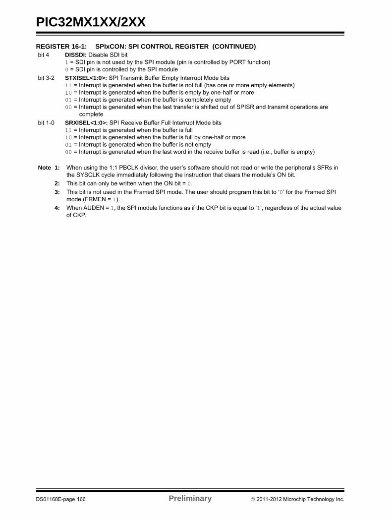
PIC32MX1XX/2XX
bit 4 DISSDI: Disable SDI bit 1 = SDI pin is not used by the SPI module (pin is controlled by PORT function)0 = SDI pin is controlled by the SPI module
bit 3-2 STXISEL<1:0>: SPI Transmit Buffer Empty Interrupt Mode bits11 = Interrupt is generated when the buffer is not full (has one or more empty elements)10 = Interrupt is generated when the buffer is empty by one-half or more01 = Interrupt is generated when the buffer is completely empty00 = Interrupt is generated when the last transfer is shifted out of SPISR and transmit operations are
complete
bit 1-0 SRXISEL<1:0>: SPI Receive Buffer Full Interrupt Mode bits11 = Interrupt is generated when the buffer is full10 = Interrupt is generated when the buffer is full by one-half or more01 = Interrupt is generated when the buffer is not empty00 = Interrupt is generated when the last word in the receive buffer is read (i.e., buffer is empty)
REGISTER 16-1: SPIxCON: SPI CONTROL REGISTER (CONTINUED)
Note 1: When using the 1:1 PBCLK divisor, the user’s software should not read or write the peripheral’s SFRs in the SYSCLK cycle immediately following the instruction that clears the module’s ON bit.
2: This bit can only be written when the ON bit = 0.
3: This bit is not used in the Framed SPI mode. The user should program this bit to ‘0’ for the Framed SPI mode (FRMEN = 1).
4: When AUDEN = 1, the SPI module functions as if the CKP bit is equal to ‘1’, regardless of the actual value of CKP.
DS61168E-page 166 Preliminary 2011-2012 Microchip Technology Inc.
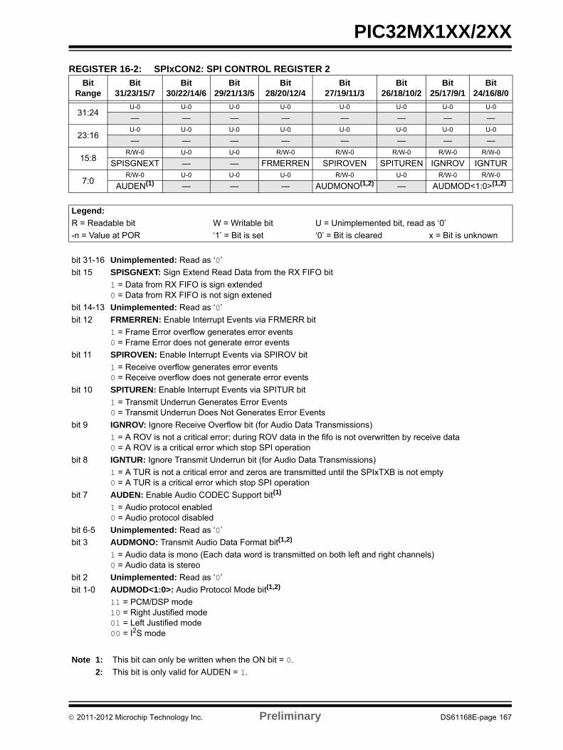
PIC32MX1XX/2XX
REGISTER 16-2: SPIxCON2: SPI CONTROL REGISTER 2
Bit Range
Bit31/23/15/7
Bit30/22/14/6
Bit29/21/13/5
Bit28/20/12/4
Bit27/19/11/3
Bit26/18/10/2
Bit25/17/9/1
Bit24/16/8/0
31:24U-0 U-0 U-0 U-0 U-0 U-0 U-0 U-0
— — — — — — — —
23:16U-0 U-0 U-0 U-0 U-0 U-0 U-0 U-0
— — — — — — — —
15:8R/W-0 U-0 U-0 R/W-0 R/W-0 R/W-0 R/W-0 R/W-0
SPISGNEXT — — FRMERREN SPIROVEN SPITUREN IGNROV IGNTUR
7:0R/W-0 U-0 U-0 U-0 R/W-0 U-0 R/W-0 R/W-0
AUDEN(1) — — — AUDMONO(1,2) — AUDMOD<1:0>(1,2)
Legend:
R = Readable bit W = Writable bit U = Unimplemented bit, read as ‘0’
-n = Value at POR ‘1’ = Bit is set ‘0’ = Bit is cleared x = Bit is unknown
bit 31-16 Unimplemented: Read as ‘0’
bit 15 SPISGNEXT: Sign Extend Read Data from the RX FIFO bit
1 = Data from RX FIFO is sign extended0 = Data from RX FIFO is not sign extened
bit 14-13 Unimplemented: Read as ‘0’
bit 12 FRMERREN: Enable Interrupt Events via FRMERR bit
1 = Frame Error overflow generates error events0 = Frame Error does not generate error events
bit 11 SPIROVEN: Enable Interrupt Events via SPIROV bit
1 = Receive overflow generates error events0 = Receive overflow does not generate error events
bit 10 SPITUREN: Enable Interrupt Events via SPITUR bit
1 = Transmit Underrun Generates Error Events0 = Transmit Underrun Does Not Generates Error Events
bit 9 IGNROV: Ignore Receive Overflow bit (for Audio Data Transmissions)
1 = A ROV is not a critical error; during ROV data in the fifo is not overwritten by receive data0 = A ROV is a critical error which stop SPI operation
bit 8 IGNTUR: Ignore Transmit Underrun bit (for Audio Data Transmissions)
1 = A TUR is not a critical error and zeros are transmitted until the SPIxTXB is not empty0 = A TUR is a critical error which stop SPI operation
bit 7 AUDEN: Enable Audio CODEC Support bit(1)
1 = Audio protocol enabled0 = Audio protocol disabled
bit 6-5 Unimplemented: Read as ‘0’
bit 3 AUDMONO: Transmit Audio Data Format bit(1,2)
1 = Audio data is mono (Each data word is transmitted on both left and right channels)0 = Audio data is stereo
bit 2 Unimplemented: Read as ‘0’
bit 1-0 AUDMOD<1:0>: Audio Protocol Mode bit(1,2)
11 = PCM/DSP mode10 = Right Justified mode01 = Left Justified mode00 = I2S mode
Note 1: This bit can only be written when the ON bit = 0.
2: This bit is only valid for AUDEN = 1.
2011-2012 Microchip Technology Inc. Preliminary DS61168E-page 167
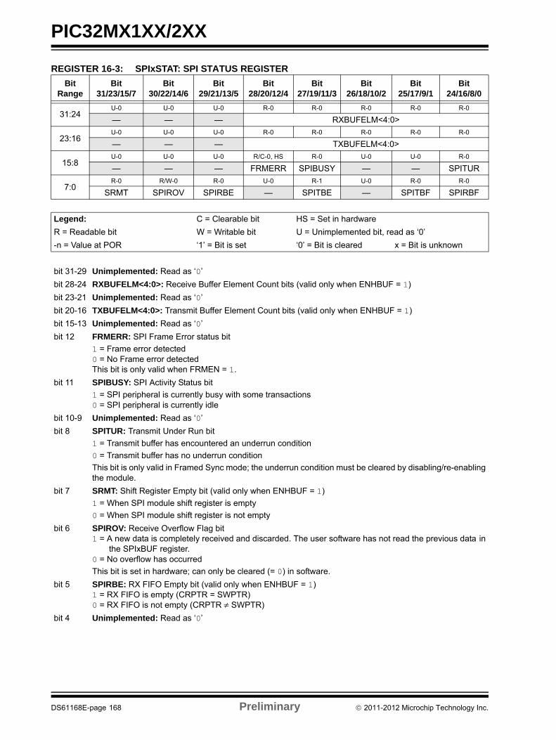
PIC32MX1XX/2XX
REGISTER 16-3: SPIxSTAT: SPI STATUS REGISTER
Bit Range
Bit31/23/15/7
Bit30/22/14/6
Bit29/21/13/5
Bit28/20/12/4
Bit27/19/11/3
Bit26/18/10/2
Bit25/17/9/1
Bit24/16/8/0
31:24U-0 U-0 U-0 R-0 R-0 R-0 R-0 R-0
— — — RXBUFELM<4:0>
23:16U-0 U-0 U-0 R-0 R-0 R-0 R-0 R-0
— — — TXBUFELM<4:0>
15:8U-0 U-0 U-0 R/C-0, HS R-0 U-0 U-0 R-0
— — — FRMERR SPIBUSY — — SPITUR
7:0R-0 R/W-0 R-0 U-0 R-1 U-0 R-0 R-0
SRMT SPIROV SPIRBE — SPITBE — SPITBF SPIRBF
Legend: C = Clearable bit HS = Set in hardware
R = Readable bit W = Writable bit U = Unimplemented bit, read as ‘0’
-n = Value at POR ‘1’ = Bit is set ‘0’ = Bit is cleared x = Bit is unknown
bit 31-29 Unimplemented: Read as ‘0’
bit 28-24 RXBUFELM<4:0>: Receive Buffer Element Count bits (valid only when ENHBUF = 1)
bit 23-21 Unimplemented: Read as ‘0’
bit 20-16 TXBUFELM<4:0>: Transmit Buffer Element Count bits (valid only when ENHBUF = 1)
bit 15-13 Unimplemented: Read as ‘0’
bit 12 FRMERR: SPI Frame Error status bit
1 = Frame error detected0 = No Frame error detectedThis bit is only valid when FRMEN = 1.
bit 11 SPIBUSY: SPI Activity Status bit
1 = SPI peripheral is currently busy with some transactions0 = SPI peripheral is currently idle
bit 10-9 Unimplemented: Read as ‘0’
bit 8 SPITUR: Transmit Under Run bit
1 = Transmit buffer has encountered an underrun condition
0 = Transmit buffer has no underrun condition
This bit is only valid in Framed Sync mode; the underrun condition must be cleared by disabling/re-enablingthe module.
bit 7 SRMT: Shift Register Empty bit (valid only when ENHBUF = 1)
1 = When SPI module shift register is empty
0 = When SPI module shift register is not empty
bit 6 SPIROV: Receive Overflow Flag bit1 = A new data is completely received and discarded. The user software has not read the previous data in
the SPIxBUF register.0 = No overflow has occurred
This bit is set in hardware; can only be cleared (= 0) in software.
bit 5 SPIRBE: RX FIFO Empty bit (valid only when ENHBUF = 1)1 = RX FIFO is empty (CRPTR = SWPTR)0 = RX FIFO is not empty (CRPTR SWPTR)
bit 4 Unimplemented: Read as ‘0’
DS61168E-page 168 Preliminary 2011-2012 Microchip Technology Inc.
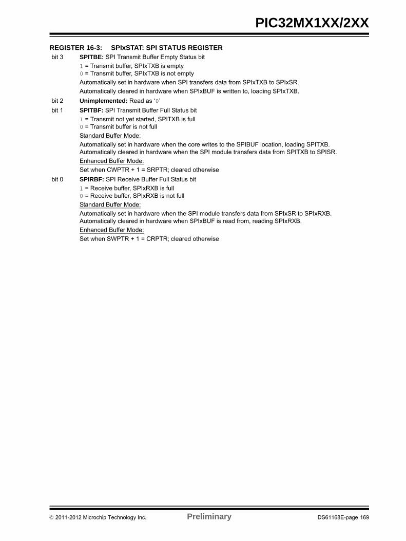
PIC32MX1XX/2XX
bit 3 SPITBE: SPI Transmit Buffer Empty Status bit
1 = Transmit buffer, SPIxTXB is empty0 = Transmit buffer, SPIxTXB is not empty
Automatically set in hardware when SPI transfers data from SPIxTXB to SPIxSR.
Automatically cleared in hardware when SPIxBUF is written to, loading SPIxTXB.
bit 2 Unimplemented: Read as ‘0’
bit 1 SPITBF: SPI Transmit Buffer Full Status bit
1 = Transmit not yet started, SPITXB is full0 = Transmit buffer is not full
Standard Buffer Mode:
Automatically set in hardware when the core writes to the SPIBUF location, loading SPITXB.Automatically cleared in hardware when the SPI module transfers data from SPITXB to SPISR.
Enhanced Buffer Mode:
Set when CWPTR + 1 = SRPTR; cleared otherwise
bit 0 SPIRBF: SPI Receive Buffer Full Status bit
1 = Receive buffer, SPIxRXB is full0 = Receive buffer, SPIxRXB is not full
Standard Buffer Mode:
Automatically set in hardware when the SPI module transfers data from SPIxSR to SPIxRXB.Automatically cleared in hardware when SPIxBUF is read from, reading SPIxRXB.
Enhanced Buffer Mode:
Set when SWPTR + 1 = CRPTR; cleared otherwise
REGISTER 16-3: SPIxSTAT: SPI STATUS REGISTER
2011-2012 Microchip Technology Inc. Preliminary DS61168E-page 169
PIC32MX1XX/2XX
NOTES:
DS61168E-page 170 Preliminary 2011-2012 Microchip Technology Inc.
PIC32MX1XX/2XX
17.0 INTER-INTEGRATED CIRCUIT™ (I2C™)
The I2C module provides complete hardware supportfor both Slave and Multi-Master modes of the I2C serialcommunication standard. Figure 17-1 illustrates theI2C module block diagram.
Each I2C module has a 2-pin interface: the SCLx pin isclock and the SDAx pin is data.
Each I2C module offers the following key features:
• I2C interface supporting both master and slave operation
• I2C Slave mode supports 7-bit and 10-bit addressing
• I2C Master mode supports 7-bit and 10-bit addressing
• I2C port allows bidirectional transfers between master and slaves
• Serial clock synchronization for the I2C port can be used as a handshake mechanism to suspend and resume serial transfer (SCLREL control)
• I2C supports multi-master operation; detects bus collision and arbitrates accordingly
• Provides support for address bit masking
Note 1: This data sheet summarizes the featuresof the PIC32MX1XX/2XX family ofdevices. It is not intended to be acomprehensive reference source. Tocomplement the information in this datasheet, refer to Section 24. “Inter-Integrated Circuit™ (I2C™)” (DS61116)in the “PIC32 Family Reference Manual”,which is available from the Microchip website (www.microchip.com/PIC32).
2: Some registers and associated bitsdescribed in this section may not beavailable on all devices. Refer toSection 4.0 “Memory Organization” inthis data sheet for device-specific registerand bit information.
2011-2012 Microchip Technology Inc. Preliminary DS61168E-page 171
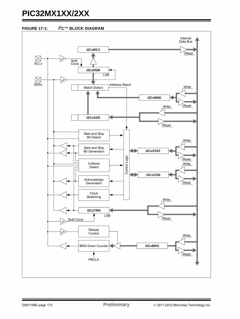
PIC32MX1XX/2XX
FIGURE 17-1: I2C™ BLOCK DIAGRAM
InternalData Bus
SCLx
SDAx
Shift
Match Detect
I2CxADD
Start and StopBit Detect
Clock
Address Match
ClockStretching
I2CxTRN
LSBShift Clock
BRG Down Counter
ReloadControl
PBCLK
Start and StopBit Generation
AcknowledgeGeneration
CollisionDetect
I2CxCON
I2CxSTAT
Con
trol
Log
ic
Read
LSB
Write
Read
I2CxBRG
I2CxRSR
Write
Read
Write
Read
Write
Read
Write
Read
Write
Read
I2CxMSK
I2CxRCV
DS61168E-page 172 Preliminary 2011-2012 Microchip Technology Inc.
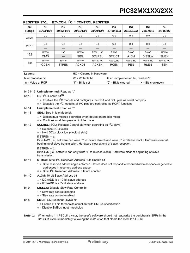
PIC32MX1XX/2XX
REGISTER 17-1: I2CXCON: I2C™ CONTROL REGISTER
Bit Range
Bit31/23/15/7
Bit30/22/14/6
Bit29/21/13/5
Bit28/20/12/4
Bit27/19/11/3
Bit26/18/10/2
Bit25/17/9/1
Bit24/16/8/0
31:24U-0 U-0 U-0 U-0 U-0 U-0 U-0 U-0
— — — — — — — —
23:16U-0 U-0 U-0 U-0 U-0 U-0 U-0 U-0
— — — — — — — —
15:8R/W-0 U-0 R/W-0 R/W-1, HC R/W-0 R/W-0 R/W-0 R/W-0
ON(1) — SIDL SCLREL STRICT A10M DISSLW SMEN
7:0R/W-0 R/W-0 R/W-0 R/W-0, HC R/W-0, HC R/W-0, HC R/W-0, HC R/W-0, HC
GCEN STREN ACKDT ACKEN RCEN PEN RSEN SEN
Legend: HC = Cleared in Hardware
R = Readable bit W = Writable bit U = Unimplemented bit, read as ‘0’
-n = Value at POR ‘1’ = Bit is set ‘0’ = Bit is cleared x = Bit is unknown
bit 31-16 Unimplemented: Read as ‘0’
bit 15 ON: I2C Enable bit(1)
1 = Enables the I2C module and configures the SDA and SCL pins as serial port pins0 = Disables the I2C module; all I2C pins are controlled by PORT functions
bit 14 Unimplemented: Read as ‘0’
bit 13 SIDL: Stop in Idle Mode bit
1 = Discontinue module operation when device enters Idle mode0 = Continue module operation in Idle mode
bit 12 SCLREL: SCLx Release Control bit (when operating as I2C slave)
1 = Release SCLx clock0 = Hold SCLx clock low (clock stretch)
If STREN = 1:Bit is R/W (i.e., software can write ‘0’ to initiate stretch and write ‘1’ to release clock). Hardware clear at beginning of slave transmission. Hardware clear at end of slave reception.
If STREN = 0:Bit is R/S (i.e., software can only write ‘1’ to release clock). Hardware clear at beginning of slavetransmission.
bit 11 STRICT: Strict I2C Reserved Address Rule Enable bit
1 = Strict reserved addressing is enforced. Device does not respond to reserved address space or generateaddresses in reserved address space.
0 = Strict I2C Reserved Address Rule not enabled
bit 10 A10M: 10-bit Slave Address bit
1 = I2CxADD is a 10-bit slave address0 = I2CxADD is a 7-bit slave address
bit 9 DISSLW: Disable Slew Rate Control bit
1 = Slew rate control disabled0 = Slew rate control enabled
bit 8 SMEN: SMBus Input Levels bit
1 = Enable I/O pin thresholds compliant with SMBus specification0 = Disable SMBus input thresholds
Note 1: When using 1:1 PBCLK divisor, the user’s software should not read/write the peripheral’s SFRs in the SYSCLK cycle immediately following the instruction that clears the module’s ON bit.
2011-2012 Microchip Technology Inc. Preliminary DS61168E-page 173
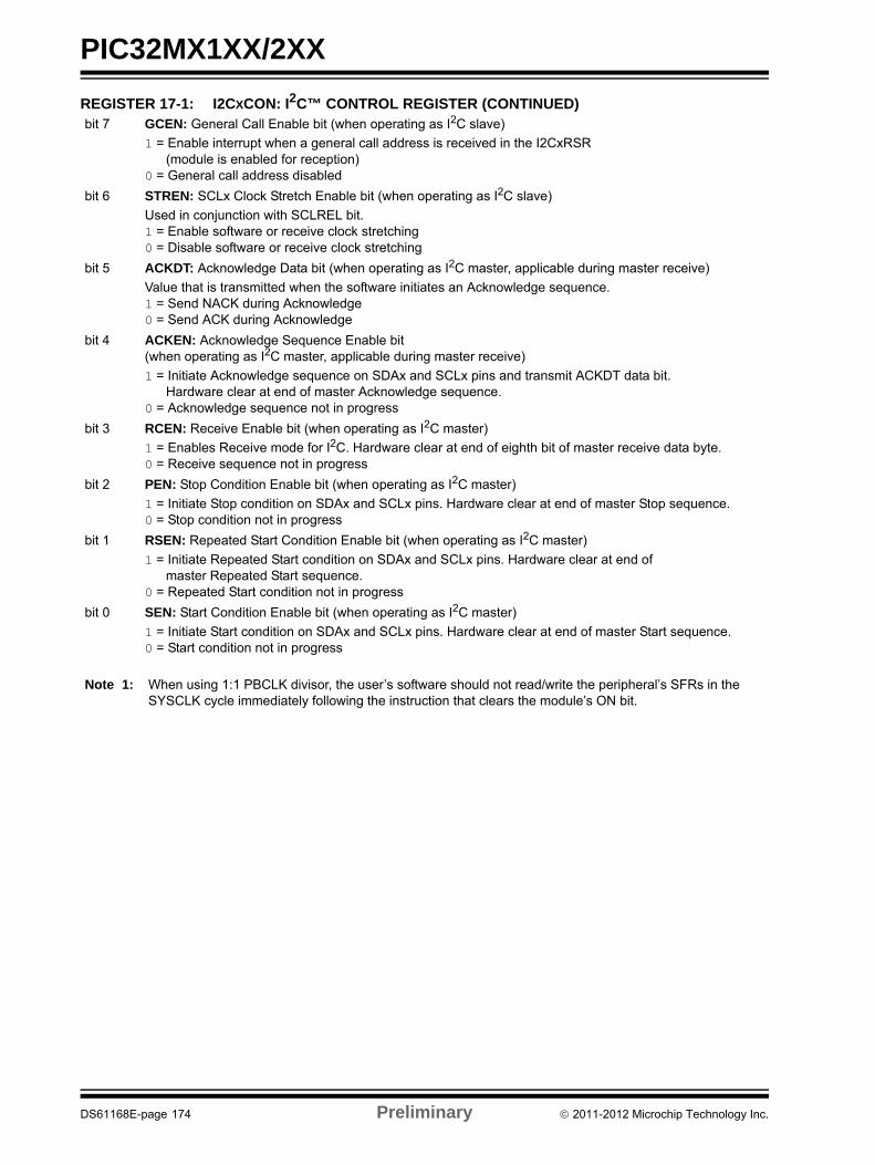
PIC32MX1XX/2XX
bit 7 GCEN: General Call Enable bit (when operating as I2C slave)
1 = Enable interrupt when a general call address is received in the I2CxRSR(module is enabled for reception)
0 = General call address disabled
bit 6 STREN: SCLx Clock Stretch Enable bit (when operating as I2C slave)
Used in conjunction with SCLREL bit.1 = Enable software or receive clock stretching0 = Disable software or receive clock stretching
bit 5 ACKDT: Acknowledge Data bit (when operating as I2C master, applicable during master receive)
Value that is transmitted when the software initiates an Acknowledge sequence.1 = Send NACK during Acknowledge0 = Send ACK during Acknowledge
bit 4 ACKEN: Acknowledge Sequence Enable bit (when operating as I2C master, applicable during master receive)
1 = Initiate Acknowledge sequence on SDAx and SCLx pins and transmit ACKDT data bit. Hardware clear at end of master Acknowledge sequence.
0 = Acknowledge sequence not in progress
bit 3 RCEN: Receive Enable bit (when operating as I2C master)
1 = Enables Receive mode for I2C. Hardware clear at end of eighth bit of master receive data byte.0 = Receive sequence not in progress
bit 2 PEN: Stop Condition Enable bit (when operating as I2C master)
1 = Initiate Stop condition on SDAx and SCLx pins. Hardware clear at end of master Stop sequence.0 = Stop condition not in progress
bit 1 RSEN: Repeated Start Condition Enable bit (when operating as I2C master)
1 = Initiate Repeated Start condition on SDAx and SCLx pins. Hardware clear at end of master Repeated Start sequence.
0 = Repeated Start condition not in progress
bit 0 SEN: Start Condition Enable bit (when operating as I2C master)
1 = Initiate Start condition on SDAx and SCLx pins. Hardware clear at end of master Start sequence.0 = Start condition not in progress
REGISTER 17-1: I2CXCON: I2C™ CONTROL REGISTER (CONTINUED)
Note 1: When using 1:1 PBCLK divisor, the user’s software should not read/write the peripheral’s SFRs in the SYSCLK cycle immediately following the instruction that clears the module’s ON bit.
DS61168E-page 174 Preliminary 2011-2012 Microchip Technology Inc.
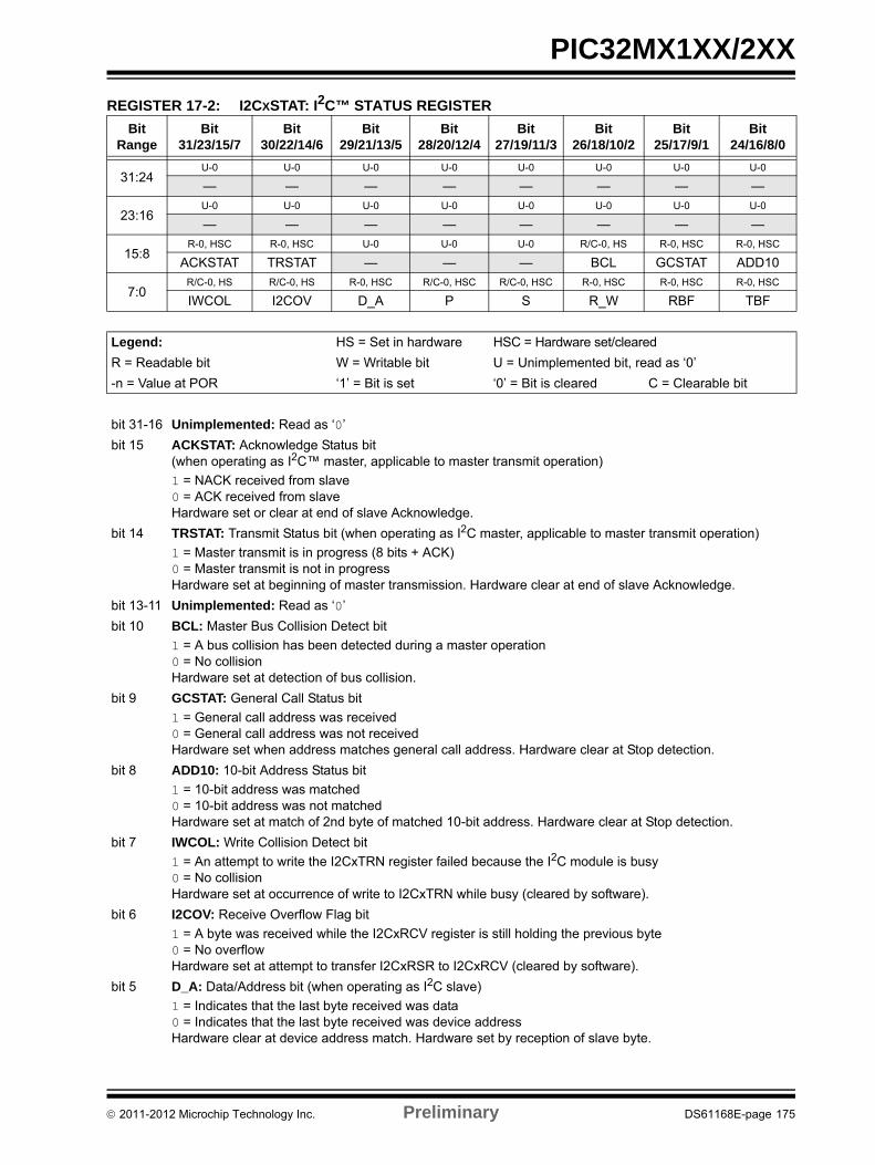
PIC32MX1XX/2XX
REGISTER 17-2: I2CXSTAT: I2C™ STATUS REGISTER
Bit Range
Bit31/23/15/7
Bit30/22/14/6
Bit29/21/13/5
Bit28/20/12/4
Bit27/19/11/3
Bit26/18/10/2
Bit25/17/9/1
Bit24/16/8/0
31:24U-0 U-0 U-0 U-0 U-0 U-0 U-0 U-0
— — — — — — — —
23:16U-0 U-0 U-0 U-0 U-0 U-0 U-0 U-0
— — — — — — — —
15:8R-0, HSC R-0, HSC U-0 U-0 U-0 R/C-0, HS R-0, HSC R-0, HSC
ACKSTAT TRSTAT — — — BCL GCSTAT ADD10
7:0R/C-0, HS R/C-0, HS R-0, HSC R/C-0, HSC R/C-0, HSC R-0, HSC R-0, HSC R-0, HSC
IWCOL I2COV D_A P S R_W RBF TBF
Legend: HS = Set in hardware HSC = Hardware set/cleared
R = Readable bit W = Writable bit U = Unimplemented bit, read as ‘0’
-n = Value at POR ‘1’ = Bit is set ‘0’ = Bit is cleared C = Clearable bit
bit 31-16 Unimplemented: Read as ‘0’
bit 15 ACKSTAT: Acknowledge Status bit (when operating as I2C™ master, applicable to master transmit operation)
1 = NACK received from slave0 = ACK received from slaveHardware set or clear at end of slave Acknowledge.
bit 14 TRSTAT: Transmit Status bit (when operating as I2C master, applicable to master transmit operation)
1 = Master transmit is in progress (8 bits + ACK)0 = Master transmit is not in progressHardware set at beginning of master transmission. Hardware clear at end of slave Acknowledge.
bit 13-11 Unimplemented: Read as ‘0’
bit 10 BCL: Master Bus Collision Detect bit
1 = A bus collision has been detected during a master operation0 = No collisionHardware set at detection of bus collision.
bit 9 GCSTAT: General Call Status bit
1 = General call address was received0 = General call address was not receivedHardware set when address matches general call address. Hardware clear at Stop detection.
bit 8 ADD10: 10-bit Address Status bit
1 = 10-bit address was matched0 = 10-bit address was not matchedHardware set at match of 2nd byte of matched 10-bit address. Hardware clear at Stop detection.
bit 7 IWCOL: Write Collision Detect bit
1 = An attempt to write the I2CxTRN register failed because the I2C module is busy 0 = No collisionHardware set at occurrence of write to I2CxTRN while busy (cleared by software).
bit 6 I2COV: Receive Overflow Flag bit
1 = A byte was received while the I2CxRCV register is still holding the previous byte0 = No overflowHardware set at attempt to transfer I2CxRSR to I2CxRCV (cleared by software).
bit 5 D_A: Data/Address bit (when operating as I2C slave)
1 = Indicates that the last byte received was data0 = Indicates that the last byte received was device addressHardware clear at device address match. Hardware set by reception of slave byte.
2011-2012 Microchip Technology Inc. Preliminary DS61168E-page 175
PIC32MX1XX/2XX
bit 4 P: Stop bit
1 = Indicates that a Stop bit has been detected last0 = Stop bit was not detected lastHardware set or clear when Start, Repeated Start or Stop detected.
bit 3 S: Start bit
1 = Indicates that a Start (or Repeated Start) bit has been detected last0 = Start bit was not detected lastHardware set or clear when Start, Repeated Start or Stop detected.
bit 2 R_W: Read/Write Information bit (when operating as I2C slave)
1 = Read – indicates data transfer is output from slave0 = Write – indicates data transfer is input to slaveHardware set or clear after reception of I2C device address byte.
bit 1 RBF: Receive Buffer Full Status bit
1 = Receive complete, I2CxRCV is full0 = Receive not complete, I2CxRCV is emptyHardware set when I2CxRCV is written with received byte. Hardware clear when software reads I2CxRCV.
bit 0 TBF: Transmit Buffer Full Status bit
1 = Transmit in progress, I2CxTRN is full0 = Transmit complete, I2CxTRN is emptyHardware set when software writes I2CxTRN. Hardware clear at completion of data transmission.
REGISTER 17-2: I2CXSTAT: I2C™ STATUS REGISTER (CONTINUED)
DS61168E-page 176 Preliminary 2011-2012 Microchip Technology Inc.
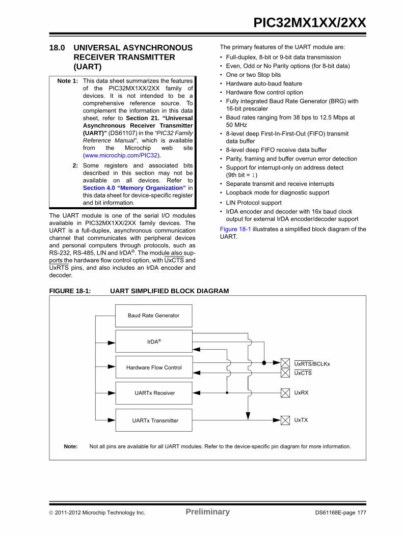
PIC32MX1XX/2XX
18.0 UNIVERSAL ASYNCHRONOUS RECEIVER TRANSMITTER (UART)
The UART module is one of the serial I/O modulesavailable in PIC32MX1XX/2XX family devices. TheUART is a full-duplex, asynchronous communicationchannel that communicates with peripheral devicesand personal computers through protocols, such asRS-232, RS-485, LIN and IrDA®. The module also sup-ports the hardware flow control option, with UxCTS andUxRTS pins, and also includes an IrDA encoder anddecoder.
The primary features of the UART module are:
• Full-duplex, 8-bit or 9-bit data transmission
• Even, Odd or No Parity options (for 8-bit data)
• One or two Stop bits
• Hardware auto-baud feature
• Hardware flow control option
• Fully integrated Baud Rate Generator (BRG) with 16-bit prescaler
• Baud rates ranging from 38 bps to 12.5 Mbps at 50 MHz
• 8-level deep First-In-First-Out (FIFO) transmit data buffer
• 8-level deep FIFO receive data buffer
• Parity, framing and buffer overrun error detection
• Support for interrupt-only on address detect (9th bit = 1)
• Separate transmit and receive interrupts
• Loopback mode for diagnostic support
• LIN Protocol support
• IrDA encoder and decoder with 16x baud clock output for external IrDA encoder/decoder support
Figure 18-1 illustrates a simplified block diagram of theUART.
FIGURE 18-1: UART SIMPLIFIED BLOCK DIAGRAM
Note 1: This data sheet summarizes the featuresof the PIC32MX1XX/2XX family ofdevices. It is not intended to be acomprehensive reference source. Tocomplement the information in this datasheet, refer to Section 21. “UniversalAsynchronous Receiver Transmitter(UART)” (DS61107) in the “PIC32 FamilyReference Manual”, which is availablefrom the Microchip web site(www.microchip.com/PIC32).
2: Some registers and associated bitsdescribed in this section may not beavailable on all devices. Refer toSection 4.0 “Memory Organization” inthis data sheet for device-specific registerand bit information.
Baud Rate Generator
UxRX
Hardware Flow Control
UARTx Receiver
UARTx Transmitter UxTX
UxCTS
UxRTS/BCLKx
IrDA®
Note: Not all pins are available for all UART modules. Refer to the device-specific pin diagram for more information.
2011-2012 Microchip Technology Inc. Preliminary DS61168E-page 177
PIC32MX1XX/2XX
REGISTER 18-1: UxMODE: UARTx MODE REGISTER
Bit Range
Bit31/23/15/7
Bit30/22/14/6
Bit29/21/13/5
Bit28/20/12/4
Bit27/19/11/3
Bit26/18/10/2
Bit25/17/9/1
Bit24/16/8/0
31:24U-0 U-0 U-0 U-0 U-0 U-0 U-0 U-0
— — — — — — — —
23:16U-0 U-0 U-0 U-0 U-0 U-0 U-0 U-0
— — — — — — — —
15:8R/W-0 U-0 R/W-0 R/W-0 R/W-0 U-0 R/W-0 R/W-0
ON(1) — SIDL IREN RTSMD — UEN<1:0>
7:0R/W-0 R/W-0 R/W-0 R/W-0 R/W-0 R/W-0 R/W-0 R/W-0
WAKE LPBACK ABAUD RXINV BRGH PDSEL<1:0> STSEL
Legend:
R = Readable bit W = Writable bit U = Unimplemented bit, read as ‘0’
-n = Value at POR ‘1’ = Bit is set ‘0’ = Bit is cleared x = Bit is unknown
bit 31-16 Unimplemented: Read as ‘0’
bit 15 ON: UARTx Enable bit(1)
1 = UARTx is enabled. UARTx pins are controlled by UARTx as defined by UEN<1:0> and UTXEN control bits
0 = UARTx is disabled. All UARTx pins are controlled by corresponding bits in the PORTx, TRISx and LATxregisters; UARTx power consumption is minimal
bit 14 Unimplemented: Read as ‘0’
bit 13 SIDL: Stop in Idle Mode bit
1 = Discontinue operation when device enters Idle mode0 = Continue operation in Idle mode
bit 12 IREN: IrDA Encoder and Decoder Enable bit
1 = IrDA is enabled0 = IrDA is disabled
bit 11 RTSMD: Mode Selection for UxRTS Pin bit
1 = UxRTS pin is in Simplex mode0 = UxRTS pin is in Flow Control mode
bit 10 Unimplemented: Read as ‘0’
bit 9-8 UEN<1:0>: UARTx Enable bits
11 = UxTX, UxRX and UxBCLK pins are enabled and used; UxCTS pin is controlled by corresponding bitsin the PORTx register
10 = UxTX, UxRX, UxCTS and UxRTS pins are enabled and used01 = UxTX, UxRX and UxRTS pins are enabled and used; UxCTS pin is controlled by corresponding bits
in the PORTx register00 = UxTX and UxRX pins are enabled and used; UxCTS and UxRTS/UxBCLK pins are controlled by
corresponding bits in the PORTx register
bit 7 WAKE: Enable Wake-up on Start bit Detect During Sleep Mode bit1 = Wake-up enabled0 = Wake-up disabled
bit 6 LPBACK: UARTx Loopback Mode Select bit1 = Loopback mode is enabled0 = Loopback mode is disabled
Note 1: When using 1:1 PBCLK divisor, the user software should not read/write the peripheral SFRs in the SYSCLK cycle immediately following the instruction that clears the module’s ON bit.
DS61168E-page 178 Preliminary 2011-2012 Microchip Technology Inc.
PIC32MX1XX/2XX
bit 5 ABAUD: Auto-Baud Enable bit1 = Enable baud rate measurement on the next character – requires reception of Sync character (0x55);
cleared by hardware upon completion0 = Baud rate measurement disabled or completed
bit 4 RXINV: Receive Polarity Inversion bit1 = UxRX Idle state is ‘0’0 = UxRX Idle state is ‘1’
bit 3 BRGH: High Baud Rate Enable bit1 = High-Speed mode – 4x baud clock enabled 0 = Standard Speed mode – 16x baud clock enabled
bit 2-1 PDSEL<1:0>: Parity and Data Selection bits11 = 9-bit data, no parity10 = 8-bit data, odd parity01 = 8-bit data, even parity00 = 8-bit data, no parity
bit 0 STSEL: Stop Selection bit1 = 2 Stop bits0 = 1 Stop bit
REGISTER 18-1: UxMODE: UARTx MODE REGISTER (CONTINUED)
Note 1: When using 1:1 PBCLK divisor, the user software should not read/write the peripheral SFRs in the SYSCLK cycle immediately following the instruction that clears the module’s ON bit.
2011-2012 Microchip Technology Inc. Preliminary DS61168E-page 179
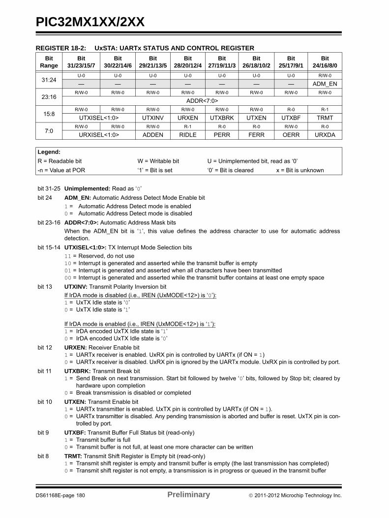
PIC32MX1XX/2XX
REGISTER 18-2: UxSTA: UARTx STATUS AND CONTROL REGISTER
Bit Range
Bit31/23/15/7
Bit30/22/14/6
Bit29/21/13/5
Bit28/20/12/4
Bit27/19/11/3
Bit26/18/10/2
Bit25/17/9/1
Bit24/16/8/0
31:24U-0 U-0 U-0 U-0 U-0 U-0 U-0 R/W-0
— — — — — — — ADM_EN
23:16R/W-0 R/W-0 R/W-0 R/W-0 R/W-0 R/W-0 R/W-0 R/W-0
ADDR<7:0>
15:8R/W-0 R/W-0 R/W-0 R/W-0 R/W-0 R/W-0 R-0 R-1
UTXISEL<1:0> UTXINV URXEN UTXBRK UTXEN UTXBF TRMT
7:0R/W-0 R/W-0 R/W-0 R-1 R-0 R-0 R/W-0 R-0
URXISEL<1:0> ADDEN RIDLE PERR FERR OERR URXDA
Legend:
R = Readable bit W = Writable bit U = Unimplemented bit, read as ‘0’
-n = Value at POR ‘1’ = Bit is set ‘0’ = Bit is cleared x = Bit is unknown
bit 31-25 Unimplemented: Read as ‘0’
bit 24 ADM_EN: Automatic Address Detect Mode Enable bit
1 = Automatic Address Detect mode is enabled0 = Automatic Address Detect mode is disabled
bit 23-16 ADDR<7:0>: Automatic Address Mask bits
When the ADM_EN bit is ‘1’, this value defines the address character to use for automatic addressdetection.
bit 15-14 UTXISEL<1:0>: TX Interrupt Mode Selection bits
11 = Reserved, do not use10 = Interrupt is generated and asserted while the transmit buffer is empty01 = Interrupt is generated and asserted when all characters have been transmitted00 = Interrupt is generated and asserted while the transmit buffer contains at least one empty space
bit 13 UTXINV: Transmit Polarity Inversion bit
If IrDA mode is disabled (i.e., IREN (UxMODE<12>) is ‘0’):1 = UxTX Idle state is ‘0’0 = UxTX Idle state is ‘1’
If IrDA mode is enabled (i.e., IREN (UxMODE<12>) is ‘1’):1 = IrDA encoded UxTX Idle state is ‘1’0 = IrDA encoded UxTX Idle state is ‘0’
bit 12 URXEN: Receiver Enable bit1 = UARTx receiver is enabled. UxRX pin is controlled by UARTx (if ON = 1)0 = UARTx receiver is disabled. UxRX pin is ignored by the UARTx module. UxRX pin is controlled by port.
bit 11 UTXBRK: Transmit Break bit1 = Send Break on next transmission. Start bit followed by twelve ‘0’ bits, followed by Stop bit; cleared by
hardware upon completion0 = Break transmission is disabled or completed
bit 10 UTXEN: Transmit Enable bit1 = UARTx transmitter is enabled. UxTX pin is controlled by UARTx (if ON = 1).0 = UARTx transmitter is disabled. Any pending transmission is aborted and buffer is reset. UxTX pin is con-
trolled by port.
bit 9 UTXBF: Transmit Buffer Full Status bit (read-only)1 = Transmit buffer is full0 = Transmit buffer is not full, at least one more character can be written
bit 8 TRMT: Transmit Shift Register is Empty bit (read-only)1 = Transmit shift register is empty and transmit buffer is empty (the last transmission has completed)0 = Transmit shift register is not empty, a transmission is in progress or queued in the transmit buffer
DS61168E-page 180 Preliminary 2011-2012 Microchip Technology Inc.
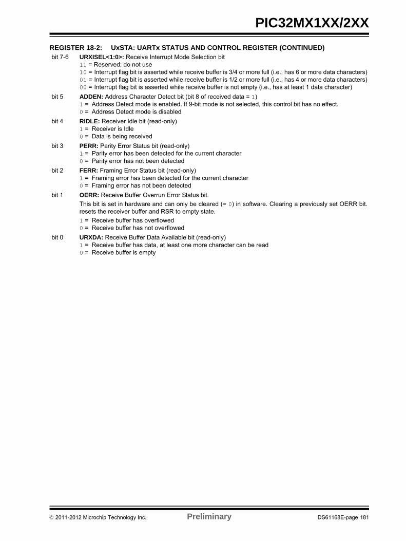
PIC32MX1XX/2XX
bit 7-6 URXISEL<1:0>: Receive Interrupt Mode Selection bit11 = Reserved; do not use10 = Interrupt flag bit is asserted while receive buffer is 3/4 or more full (i.e., has 6 or more data characters)01 = Interrupt flag bit is asserted while receive buffer is 1/2 or more full (i.e., has 4 or more data characters)00 = Interrupt flag bit is asserted while receive buffer is not empty (i.e., has at least 1 data character)
bit 5 ADDEN: Address Character Detect bit (bit 8 of received data = 1)1 = Address Detect mode is enabled. If 9-bit mode is not selected, this control bit has no effect.0 = Address Detect mode is disabled
bit 4 RIDLE: Receiver Idle bit (read-only)1 = Receiver is Idle0 = Data is being received
bit 3 PERR: Parity Error Status bit (read-only)1 = Parity error has been detected for the current character0 = Parity error has not been detected
bit 2 FERR: Framing Error Status bit (read-only)1 = Framing error has been detected for the current character0 = Framing error has not been detected
bit 1 OERR: Receive Buffer Overrun Error Status bit.
This bit is set in hardware and can only be cleared (= 0) in software. Clearing a previously set OERR bit.resets the receiver buffer and RSR to empty state.
1 = Receive buffer has overflowed0 = Receive buffer has not overflowed
bit 0 URXDA: Receive Buffer Data Available bit (read-only)1 = Receive buffer has data, at least one more character can be read0 = Receive buffer is empty
REGISTER 18-2: UxSTA: UARTx STATUS AND CONTROL REGISTER (CONTINUED)
2011-2012 Microchip Technology Inc. Preliminary DS61168E-page 181
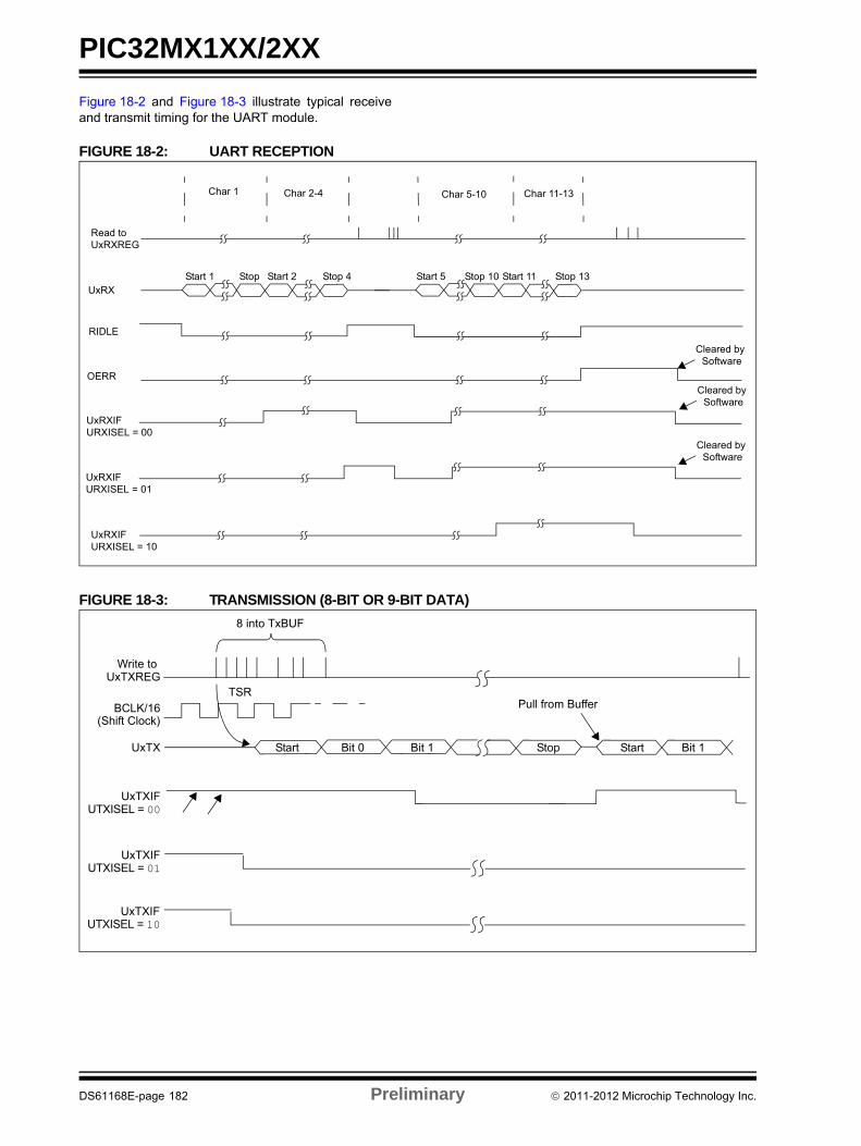
PIC32MX1XX/2XX
Figure 18-2 and Figure 18-3 illustrate typical receiveand transmit timing for the UART module.
FIGURE 18-2: UART RECEPTION
FIGURE 18-3: TRANSMISSION (8-BIT OR 9-BIT DATA)
Start 1 Stop Start 2 Stop 4 Start 5 Stop 10 Start 11 Stop 13
Read toUxRXREG
UxRX
RIDLE
OERR
UxRXIFURXISEL = 00
UxRXIFURXISEL = 01
UxRXIFURXISEL = 10
Char 1 Char 2-4 Char 5-10 Char 11-13
Cleared bySoftware
Cleared bySoftware
Cleared bySoftware
StartStart Bit 0 Bit 1 Stop
Write to
TSRBCLK/16
(Shift Clock)
UxTX
UxTXIF
UxTXIF
UTXISEL = 00
Bit 1
UxTXREG
UTXISEL = 01
UxTXIFUTXISEL = 10
8 into TxBUF
Pull from Buffer
DS61168E-page 182 Preliminary 2011-2012 Microchip Technology Inc.
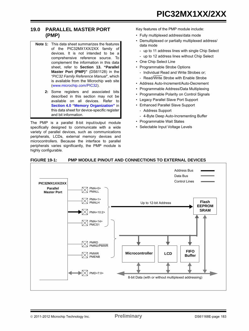
PIC32MX1XX/2XX
19.0 PARALLEL MASTER PORT (PMP)
The PMP is a parallel 8-bit input/output modulespecifically designed to communicate with a widevariety of parallel devices, such as communicationsperipherals, LCDs, external memory devices andmicrocontrollers. Because the interface to parallelperipherals varies significantly, the PMP module ishighly configurable.
Key features of the PMP module include:
• Fully multiplexed address/data mode
• Demultiplexed or partially multiplexed address/ data mode
- up to 11 address lines with single Chip Select
- up to 12 address lines without Chip Select
• One Chip Select Line
• Programmable Strobe Options
- Individual Read and Write Strobes or;
- Read/Write Strobe with Enable Strobe
• Address Auto-Increment/Auto-Decrement
• Programmable Address/Data Multiplexing
• Programmable Polarity on Control Signals
• Legacy Parallel Slave Port Support
• Enhanced Parallel Slave Support
- Address Support
- 4-Byte Deep Auto-Incrementing Buffer
• Programmable Wait States
• Selectable Input Voltage Levels
FIGURE 19-1: PMP MODULE PINOUT AND CONNECTIONS TO EXTERNAL DEVICES
Note 1: This data sheet summarizes the featuresof the PIC32MX1XX/2XX family ofdevices. It is not intended to be acomprehensive reference source. Tocomplement the information in this datasheet, refer to Section 13. “ParallelMaster Port (PMP)” (DS61128) in the“PIC32 Family Reference Manual”, whichis available from the Microchip web site(www.microchip.com/PIC32).
2: Some registers and associated bitsdescribed in this section may not beavailable on all devices. Refer toSection 4.0 “Memory Organization” inthis data sheet for device-specific registerand bit information.
PMA<0>
PMA<14>
PMRD
PMWRPMENB
PMRD/PMWR
PMCS1
PMA<1>
PMA<10:2>
PMALL
PMALH Flash
Address Bus
Data Bus
Control LinesPIC32MX1XX/2XX
LCDFIFOMicrocontroller
8-bit Data (with or without multiplexed addressing)
Up to 12-bit Address
Parallel
Buffer
PMD<7:0>
Master Port
EEPROMSRAM
2011-2012 Microchip Technology Inc. Preliminary DS61168E-page 183
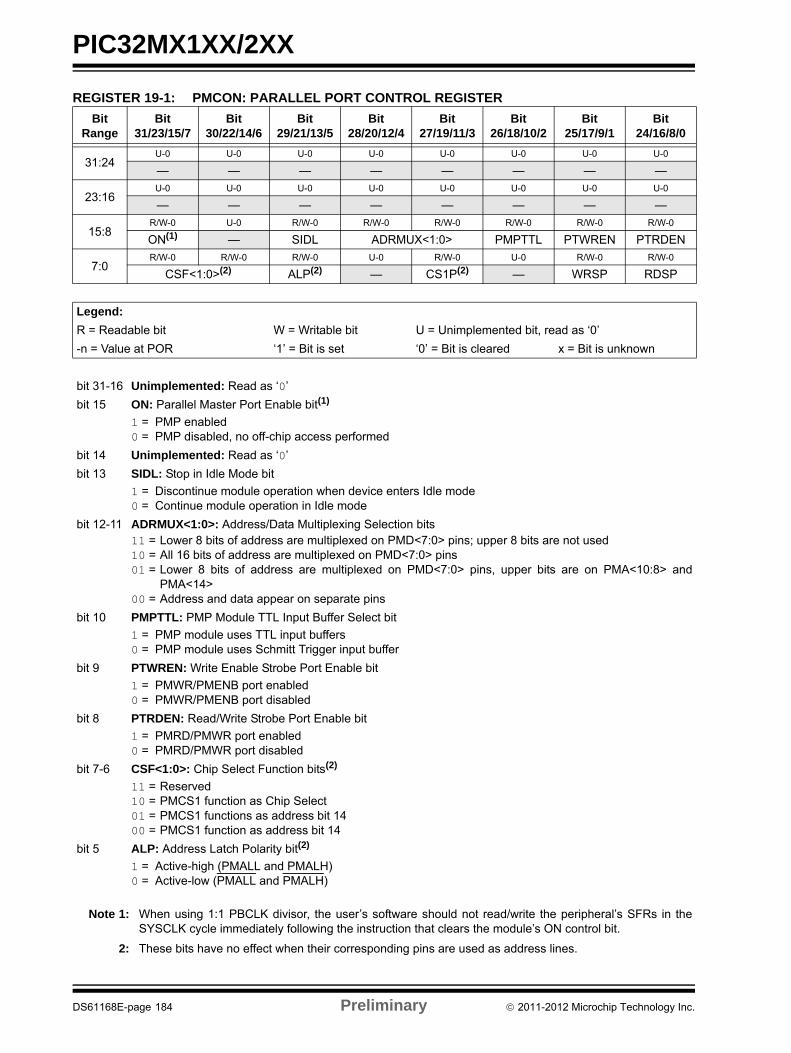
PIC32MX1XX/2XX
REGISTER 19-1: PMCON: PARALLEL PORT CONTROL REGISTER
Bit Range
Bit31/23/15/7
Bit30/22/14/6
Bit29/21/13/5
Bit28/20/12/4
Bit27/19/11/3
Bit26/18/10/2
Bit25/17/9/1
Bit24/16/8/0
31:24U-0 U-0 U-0 U-0 U-0 U-0 U-0 U-0
— — — — — — — —
23:16U-0 U-0 U-0 U-0 U-0 U-0 U-0 U-0
— — — — — — — —
15:8R/W-0 U-0 R/W-0 R/W-0 R/W-0 R/W-0 R/W-0 R/W-0
ON(1) — SIDL ADRMUX<1:0> PMPTTL PTWREN PTRDEN
7:0R/W-0 R/W-0 R/W-0 U-0 R/W-0 U-0 R/W-0 R/W-0
CSF<1:0>(2) ALP(2) — CS1P(2) — WRSP RDSP
Legend:
R = Readable bit W = Writable bit U = Unimplemented bit, read as ‘0’
-n = Value at POR ‘1’ = Bit is set ‘0’ = Bit is cleared x = Bit is unknown
bit 31-16 Unimplemented: Read as ‘0’
bit 15 ON: Parallel Master Port Enable bit(1)
1 = PMP enabled0 = PMP disabled, no off-chip access performed
bit 14 Unimplemented: Read as ‘0’
bit 13 SIDL: Stop in Idle Mode bit
1 = Discontinue module operation when device enters Idle mode0 = Continue module operation in Idle mode
bit 12-11 ADRMUX<1:0>: Address/Data Multiplexing Selection bits11 = Lower 8 bits of address are multiplexed on PMD<7:0> pins; upper 8 bits are not used10 = All 16 bits of address are multiplexed on PMD<7:0> pins01 = Lower 8 bits of address are multiplexed on PMD<7:0> pins, upper bits are on PMA<10:8> and
PMA<14>00 = Address and data appear on separate pins
bit 10 PMPTTL: PMP Module TTL Input Buffer Select bit
1 = PMP module uses TTL input buffers0 = PMP module uses Schmitt Trigger input buffer
bit 9 PTWREN: Write Enable Strobe Port Enable bit
1 = PMWR/PMENB port enabled0 = PMWR/PMENB port disabled
bit 8 PTRDEN: Read/Write Strobe Port Enable bit
1 = PMRD/PMWR port enabled0 = PMRD/PMWR port disabled
bit 7-6 CSF<1:0>: Chip Select Function bits(2)
11 = Reserved10 = PMCS1 function as Chip Select01 = PMCS1 functions as address bit 1400 = PMCS1 function as address bit 14
bit 5 ALP: Address Latch Polarity bit(2)
1 = Active-high (PMALL and PMALH)0 = Active-low (PMALL and PMALH)
Note 1: When using 1:1 PBCLK divisor, the user’s software should not read/write the peripheral’s SFRs in theSYSCLK cycle immediately following the instruction that clears the module’s ON control bit.
2: These bits have no effect when their corresponding pins are used as address lines.
DS61168E-page 184 Preliminary 2011-2012 Microchip Technology Inc.
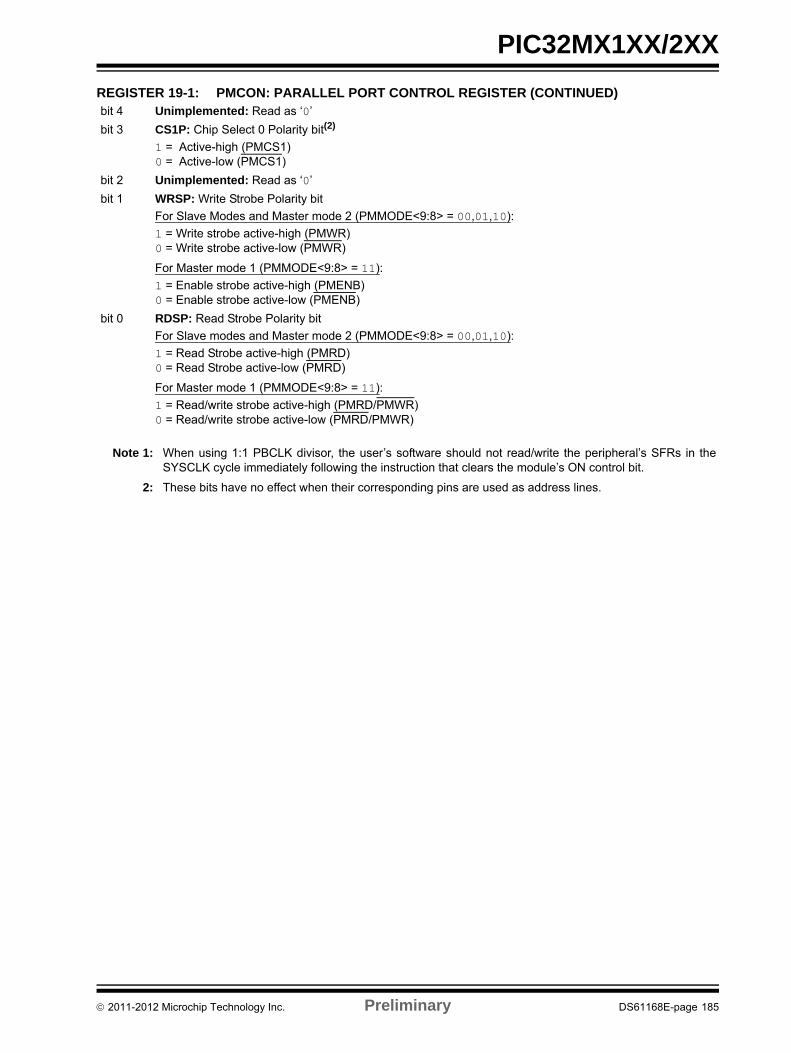
PIC32MX1XX/2XX
bit 4 Unimplemented: Read as ‘0’
bit 3 CS1P: Chip Select 0 Polarity bit(2)
1 = Active-high (PMCS1)0 = Active-low (PMCS1)
bit 2 Unimplemented: Read as ‘0’
bit 1 WRSP: Write Strobe Polarity bit
For Slave Modes and Master mode 2 (PMMODE<9:8> = 00,01,10):
1 = Write strobe active-high (PMWR)0 = Write strobe active-low (PMWR)
For Master mode 1 (PMMODE<9:8> = 11):
1 = Enable strobe active-high (PMENB)0 = Enable strobe active-low (PMENB)
bit 0 RDSP: Read Strobe Polarity bit
For Slave modes and Master mode 2 (PMMODE<9:8> = 00,01,10):
1 = Read Strobe active-high (PMRD)0 = Read Strobe active-low (PMRD)
For Master mode 1 (PMMODE<9:8> = 11):
1 = Read/write strobe active-high (PMRD/PMWR)0 = Read/write strobe active-low (PMRD/PMWR)
REGISTER 19-1: PMCON: PARALLEL PORT CONTROL REGISTER (CONTINUED)
Note 1: When using 1:1 PBCLK divisor, the user’s software should not read/write the peripheral’s SFRs in theSYSCLK cycle immediately following the instruction that clears the module’s ON control bit.
2: These bits have no effect when their corresponding pins are used as address lines.
2011-2012 Microchip Technology Inc. Preliminary DS61168E-page 185
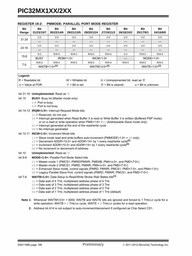
PIC32MX1XX/2XX
REGISTER 19-2: PMMODE: PARALLEL PORT MODE REGISTER
Bit Range
Bit31/23/15/7
Bit30/22/14/6
Bit29/21/13/5
Bit28/20/12/4
Bit27/19/11/3
Bit26/18/10/2
Bit25/17/9/1
Bit24/16/8/0
31:24U-0 U-0 U-0 U-0 U-0 U-0 U-0 U-0
— — — — — — — —
23:16U-0 U-0 U-0 U-0 U-0 U-0 U-0 U-0
— — — — — — — —
15:8R-0 R/W-0 R/W-0 R/W-0 R/W-0 U-0 R/W-0 R/W-0
BUSY IRQM<1:0> INCM<1:0> — MODE<1:0>
7:0R/W-0 R/W-0 R/W-0 R/W-0 R/W-0 R/W-0 R/W-0 R/W-0
WAITB<1:0>(1) WAITM<3:0>(1) WAITE<1:0>(1)
Legend:
R = Readable bit W = Writable bit U = Unimplemented bit, read as ‘0’
-n = Value at POR ‘1’ = Bit is set ‘0’ = Bit is cleared x = Bit is unknown
bit 31-16 Unimplemented: Read as ‘0’
bit 15 BUSY: Busy bit (Master mode only)
1 = Port is busy 0 = Port is not busy
bit 14-13 IRQM<1:0>: Interrupt Request Mode bits
11 = Reserved, do not use10 = Interrupt generated when Read Buffer 3 is read or Write Buffer 3 is written (Buffered PSP mode)
or on a read or write operation when PMA<1:0> =11 (Addressable Slave mode only)01 = Interrupt generated at the end of the read/write cycle00 = No Interrupt generated
bit 12-11 INCM<1:0>: Increment Mode bits
11 = Slave mode read and write buffers auto-increment (PMMODE<1:0> = 00 only)10 = Decrement ADDR<10:2> and ADDR<14> by 1 every read/write cycle(2)
01 = Increment ADDR<10:2> and ADDR<14> by 1 every read/write cycle(2)
00 = No increment or decrement of address
bit 10 Unimplemented: Read as ‘0’
bit 9-8 MODE<1:0>: Parallel Port Mode Select bits
11 = Master mode 1 (PMCS1, PMRD/PMWR, PMENB, PMA<x:0>, and PMD<7:0>)10 = Master mode 2 (PMCS1, PMRD, PMWR, PMA<x:0>, and PMD<7:0>)01 = Enhanced Slave mode, control signals (PMRD, PMWR, PMCS1, PMD<7:0>, and PMA<1:0>)00 = Legacy Parallel Slave Port, control signals (PMRD, PMWR, PMCS1, and PMD<7:0>)
bit 7-6 WAITB<1:0>: Data Setup to Read/Write Strobe Wait States bits(1)
11 = Data wait of 4 TPB; multiplexed address phase of 4 TPB
10 = Data wait of 3 TPB; multiplexed address phase of 3 TPB
01 = Data wait of 2 TPB; multiplexed address phase of 2 TPB
00 = Data wait of 1 TPB; multiplexed address phase of 1 TPB (default)
Note 1: Whenever WAITM<3:0> = 0000, WAITB and WAITE bits are ignored and forced to 1 TPBCLK cycle for awrite operation; WAITB = 1 TPBCLK cycle, WAITE = 0 TPBCLK cycles for a read operation.
2: Address bit A14 is not subject to auto-increment/decrement if configured as Chip Select CS1.
DS61168E-page 186 Preliminary 2011-2012 Microchip Technology Inc.
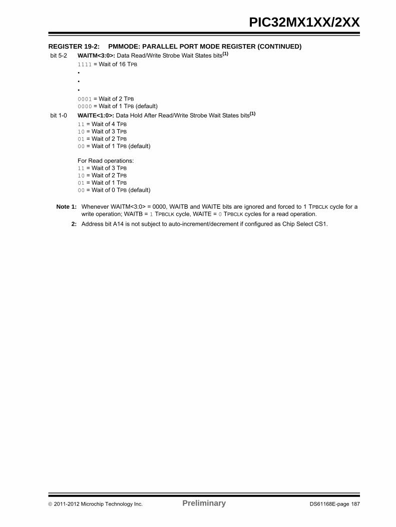
PIC32MX1XX/2XX
bit 5-2 WAITM<3:0>: Data Read/Write Strobe Wait States bits(1)
1111 = Wait of 16 TPB
•
•
•
0001 = Wait of 2 TPB
0000 = Wait of 1 TPB (default)
bit 1-0 WAITE<1:0>: Data Hold After Read/Write Strobe Wait States bits(1)
11 = Wait of 4 TPB
10 = Wait of 3 TPB
01 = Wait of 2 TPB
00 = Wait of 1 TPB (default)
For Read operations:11 = Wait of 3 TPB
10 = Wait of 2 TPB
01 = Wait of 1 TPB
00 = Wait of 0 TPB (default)
REGISTER 19-2: PMMODE: PARALLEL PORT MODE REGISTER (CONTINUED)
Note 1: Whenever WAITM<3:0> = 0000, WAITB and WAITE bits are ignored and forced to 1 TPBCLK cycle for awrite operation; WAITB = 1 TPBCLK cycle, WAITE = 0 TPBCLK cycles for a read operation.
2: Address bit A14 is not subject to auto-increment/decrement if configured as Chip Select CS1.
2011-2012 Microchip Technology Inc. Preliminary DS61168E-page 187
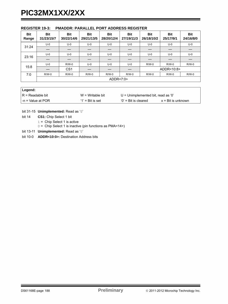
PIC32MX1XX/2XX
REGISTER 19-3: PMADDR: PARALLEL PORT ADDRESS REGISTER
Bit Range
Bit31/23/15/7
Bit30/22/14/6
Bit29/21/13/5
Bit28/20/12/4
Bit27/19/11/3
Bit26/18/10/2
Bit25/17/9/1
Bit24/16/8/0
31:24U-0 U-0 U-0 U-0 U-0 U-0 U-0 U-0
— — — — — — — —
23:16U-0 U-0 U-0 U-0 U-0 U-0 U-0 U-0
— — — — — — — —
15:8U-0 R/W-0 U-0 U-0 U-0 R/W-0 R/W-0 R/W-0
— CS1 — — — ADDR<10:8>
7:0 R/W-0 R/W-0 R/W-0 R/W-0 R/W-0 R/W-0 R/W-0 R/W-0
ADDR<7:0>
Legend:
R = Readable bit W = Writable bit U = Unimplemented bit, read as ‘0’
-n = Value at POR ‘1’ = Bit is set ‘0’ = Bit is cleared x = Bit is unknown
bit 31-15 Unimplemented: Read as ‘0’
bit 14 CS1: Chip Select 1 bit
1 = Chip Select 1 is active0 = Chip Select 1 is inactive (pin functions as PMA<14>)
bit 13-11 Unimplemented: Read as ‘0’
bit 10-0 ADDR<10:0>: Destination Address bits
DS61168E-page 188 Preliminary 2011-2012 Microchip Technology Inc.
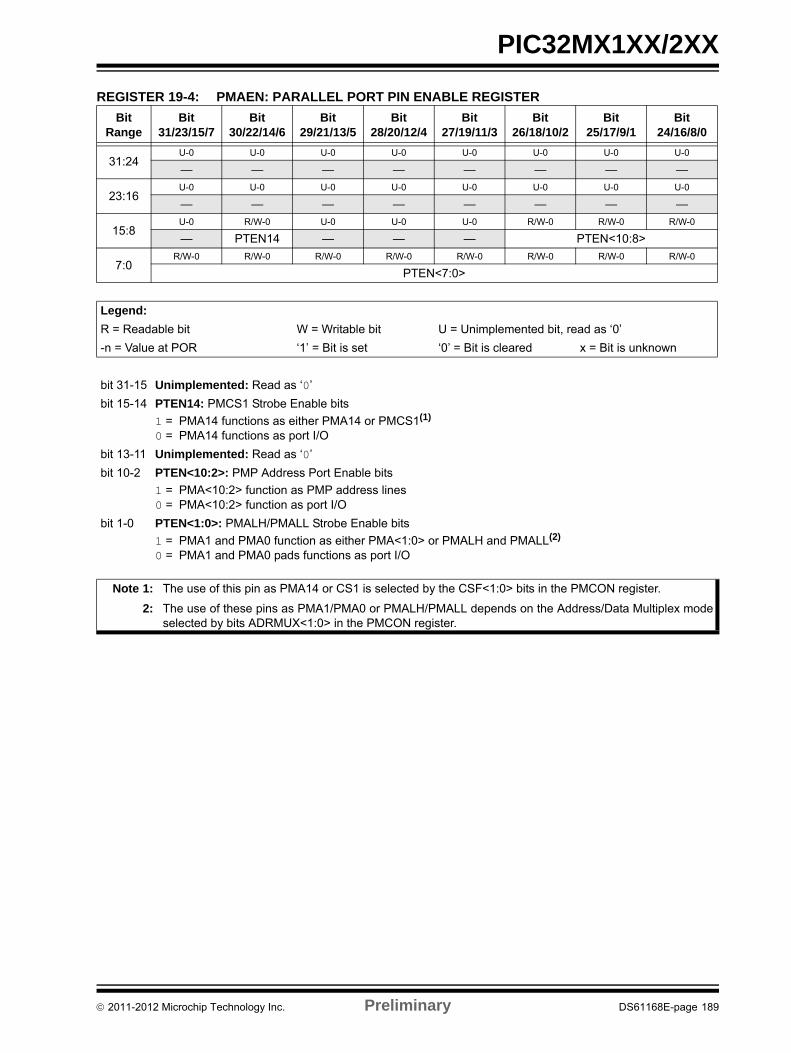
PIC32MX1XX/2XX
REGISTER 19-4: PMAEN: PARALLEL PORT PIN ENABLE REGISTER
Bit Range
Bit31/23/15/7
Bit30/22/14/6
Bit29/21/13/5
Bit28/20/12/4
Bit27/19/11/3
Bit26/18/10/2
Bit25/17/9/1
Bit24/16/8/0
31:24U-0 U-0 U-0 U-0 U-0 U-0 U-0 U-0
— — — — — — — —
23:16U-0 U-0 U-0 U-0 U-0 U-0 U-0 U-0
— — — — — — — —
15:8U-0 R/W-0 U-0 U-0 U-0 R/W-0 R/W-0 R/W-0
— PTEN14 — — — PTEN<10:8>
7:0R/W-0 R/W-0 R/W-0 R/W-0 R/W-0 R/W-0 R/W-0 R/W-0
PTEN<7:0>
Legend:
R = Readable bit W = Writable bit U = Unimplemented bit, read as ‘0’
-n = Value at POR ‘1’ = Bit is set ‘0’ = Bit is cleared x = Bit is unknown
bit 31-15 Unimplemented: Read as ‘0’
bit 15-14 PTEN14: PMCS1 Strobe Enable bits
1 = PMA14 functions as either PMA14 or PMCS1(1)
0 = PMA14 functions as port I/O
bit 13-11 Unimplemented: Read as ‘0’
bit 10-2 PTEN<10:2>: PMP Address Port Enable bits
1 = PMA<10:2> function as PMP address lines0 = PMA<10:2> function as port I/O
bit 1-0 PTEN<1:0>: PMALH/PMALL Strobe Enable bits
1 = PMA1 and PMA0 function as either PMA<1:0> or PMALH and PMALL(2)
0 = PMA1 and PMA0 pads functions as port I/O
Note 1: The use of this pin as PMA14 or CS1 is selected by the CSF<1:0> bits in the PMCON register.
2: The use of these pins as PMA1/PMA0 or PMALH/PMALL depends on the Address/Data Multiplex modeselected by bits ADRMUX<1:0> in the PMCON register.
2011-2012 Microchip Technology Inc. Preliminary DS61168E-page 189
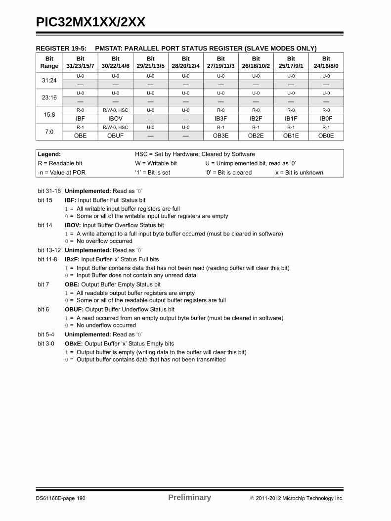
PIC32MX1XX/2XX
REGISTER 19-5: PMSTAT: PARALLEL PORT STATUS REGISTER (SLAVE MODES ONLY)
Bit Range
Bit31/23/15/7
Bit30/22/14/6
Bit29/21/13/5
Bit28/20/12/4
Bit27/19/11/3
Bit26/18/10/2
Bit25/17/9/1
Bit24/16/8/0
31:24U-0 U-0 U-0 U-0 U-0 U-0 U-0 U-0
— — — — — — — —
23:16U-0 U-0 U-0 U-0 U-0 U-0 U-0 U-0
— — — — — — — —
15:8R-0 R/W-0, HSC U-0 U-0 R-0 R-0 R-0 R-0
IBF IBOV — — IB3F IB2F IB1F IB0F
7:0R-1 R/W-0, HSC U-0 U-0 R-1 R-1 R-1 R-1
OBE OBUF — — OB3E OB2E OB1E OB0E
Legend: HSC = Set by Hardware; Cleared by Software
R = Readable bit W = Writable bit U = Unimplemented bit, read as ‘0’
-n = Value at POR ‘1’ = Bit is set ‘0’ = Bit is cleared x = Bit is unknown
bit 31-16 Unimplemented: Read as ‘0’
bit 15 IBF: Input Buffer Full Status bit
1 = All writable input buffer registers are full0 = Some or all of the writable input buffer registers are empty
bit 14 IBOV: Input Buffer Overflow Status bit
1 = A write attempt to a full input byte buffer occurred (must be cleared in software)0 = No overflow occurred
bit 13-12 Unimplemented: Read as ‘0’
bit 11-8 IBxF: Input Buffer ‘x’ Status Full bits
1 = Input Buffer contains data that has not been read (reading buffer will clear this bit)0 = Input Buffer does not contain any unread data
bit 7 OBE: Output Buffer Empty Status bit
1 = All readable output buffer registers are empty0 = Some or all of the readable output buffer registers are full
bit 6 OBUF: Output Buffer Underflow Status bit
1 = A read occurred from an empty output byte buffer (must be cleared in software)0 = No underflow occurred
bit 5-4 Unimplemented: Read as ‘0’
bit 3-0 OBxE: Output Buffer ‘x’ Status Empty bits
1 = Output buffer is empty (writing data to the buffer will clear this bit)0 = Output buffer contains data that has not been transmitted
DS61168E-page 190 Preliminary 2011-2012 Microchip Technology Inc.
PIC32MX1XX/2XX
20.0 REAL-TIME CLOCK AND CALENDAR (RTCC)
The PIC32 RTCC module is intended for applications inwhich accurate time must be maintained for extendedperiods of time with minimal or no CPU intervention.Low-power optimization provides extended batterylifetime while keeping track of time.
Following are some of the key features of this module:
• Time: hours, minutes and seconds
• 24-hour format (military time)
• Visibility of one-half second period
• Provides calendar: Weekday, date, month and year
• Alarm intervals are configurable for half of a second, one second, 10 seconds, one minute, 10 minutes, one hour, one day, one week, one month and one year
• Alarm repeat with decrementing counter
• Alarm with indefinite repeat: Chime
• Year range: 2000 to 2099
• Leap year correction
• BCD format for smaller firmware overhead
• Optimized for long-term battery operation
• Fractional second synchronization
• User calibration of the clock crystal frequency with auto-adjust
• Calibration range: 0.66 seconds error per month
• Calibrates up to 260 ppm of crystal error
• Requirements: External 32.768 kHz clock crystal
• Alarm pulse or seconds clock output on RTCC pin
FIGURE 20-1: RTCC BLOCK DIAGRAM
Note 1: This data sheet summarizes the featuresof the PIC32MX1XX/2XX family ofdevices. It is not intended to be acomprehensive reference source. Tocomplement the information in this datasheet, refer to Section 29. “Real-TimeClock and Calendar (RTCC)”(DS61125) in the “PIC32 FamilyReference Manual”, which is availablefrom the Microchip web site(www.microchip.com/PIC32).
2: Some registers and associated bitsdescribed in this section may not beavailable on all devices. Refer toSection 4.0 “Memory Organization” inthis data sheet for device-specific registerand bit information.
RTCC Prescalers
RTCC Timer
Comparator
Compare Registers
Repeat Counter
ALRMTIME
HR, MIN, SEC
ALRMDATEwith Masks
RTCC Interrupt Logic
AlarmEvent
32.768 kHz Inputfrom Secondary
0.5s
Alarm Pulse
Set RTCC Flag
RTCVAL
ALRMVAL
RTCC
RTCOE
Oscillator (SOSC)
CAL<9:0>
MONTH, DAY, WDAY
RTCTIME
HR, MIN, SEC
RTCDATE
YEAR, MONTH, DAY, WDAY
Seconds Pulse
RTSECSEL
0
1
2011-2012 Microchip Technology Inc. Preliminary DS61168E-page 191
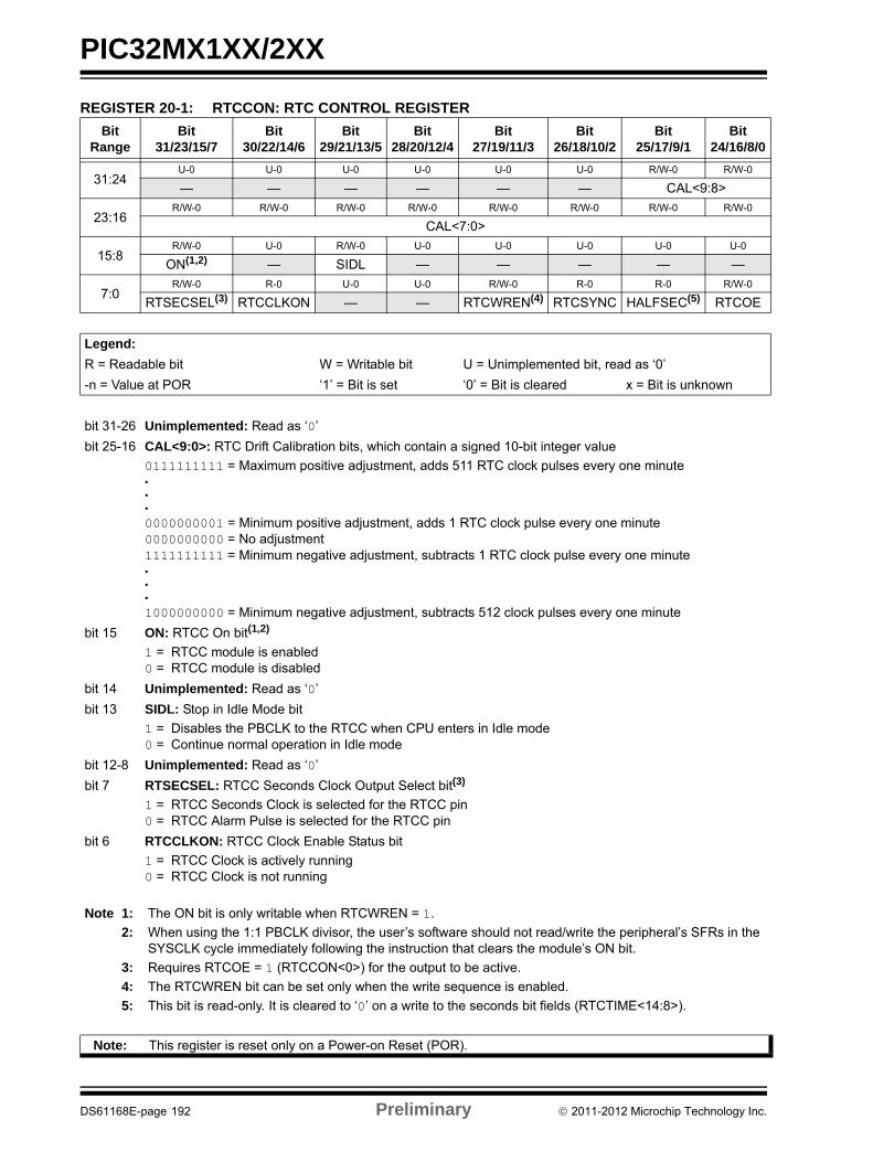
PIC32MX1XX/2XX
REGISTER 20-1: RTCCON: RTC CONTROL REGISTER
Bit Range
Bit31/23/15/7
Bit30/22/14/6
Bit29/21/13/5
Bit28/20/12/4
Bit27/19/11/3
Bit26/18/10/2
Bit25/17/9/1
Bit24/16/8/0
31:24U-0 U-0 U-0 U-0 U-0 U-0 R/W-0 R/W-0
— — — — — — CAL<9:8>
23:16R/W-0 R/W-0 R/W-0 R/W-0 R/W-0 R/W-0 R/W-0 R/W-0
CAL<7:0>
15:8R/W-0 U-0 R/W-0 U-0 U-0 U-0 U-0 U-0
ON(1,2) — SIDL — — — — —
7:0R/W-0 R-0 U-0 U-0 R/W-0 R-0 R-0 R/W-0
RTSECSEL(3) RTCCLKON — — RTCWREN(4) RTCSYNC HALFSEC(5) RTCOE
Legend:
R = Readable bit W = Writable bit U = Unimplemented bit, read as ‘0’
-n = Value at POR ‘1’ = Bit is set ‘0’ = Bit is cleared x = Bit is unknown
bit 31-26 Unimplemented: Read as ‘0’
bit 25-16 CAL<9:0>: RTC Drift Calibration bits, which contain a signed 10-bit integer value
0111111111 = Maximum positive adjustment, adds 511 RTC clock pulses every one minute•••
0000000001 = Minimum positive adjustment, adds 1 RTC clock pulse every one minute0000000000 = No adjustment1111111111 = Minimum negative adjustment, subtracts 1 RTC clock pulse every one minute•••
1000000000 = Minimum negative adjustment, subtracts 512 clock pulses every one minute
bit 15 ON: RTCC On bit(1,2)
1 = RTCC module is enabled0 = RTCC module is disabled
bit 14 Unimplemented: Read as ‘0’
bit 13 SIDL: Stop in Idle Mode bit
1 = Disables the PBCLK to the RTCC when CPU enters in Idle mode0 = Continue normal operation in Idle mode
bit 12-8 Unimplemented: Read as ‘0’
bit 7 RTSECSEL: RTCC Seconds Clock Output Select bit(3)
1 = RTCC Seconds Clock is selected for the RTCC pin0 = RTCC Alarm Pulse is selected for the RTCC pin
bit 6 RTCCLKON: RTCC Clock Enable Status bit
1 = RTCC Clock is actively running0 = RTCC Clock is not running
Note 1: The ON bit is only writable when RTCWREN = 1.
2: When using the 1:1 PBCLK divisor, the user’s software should not read/write the peripheral’s SFRs in the SYSCLK cycle immediately following the instruction that clears the module’s ON bit.
3: Requires RTCOE = 1 (RTCCON<0>) for the output to be active.
4: The RTCWREN bit can be set only when the write sequence is enabled.
5: This bit is read-only. It is cleared to ‘0’ on a write to the seconds bit fields (RTCTIME<14:8>).
Note: This register is reset only on a Power-on Reset (POR).
DS61168E-page 192 Preliminary 2011-2012 Microchip Technology Inc.
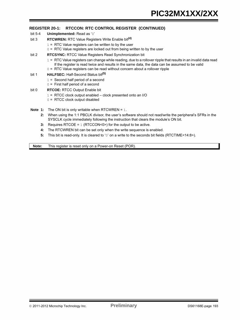
PIC32MX1XX/2XX
bit 5-4 Unimplemented: Read as ‘0’
bit 3 RTCWREN: RTC Value Registers Write Enable bit(4)
1 = RTC Value registers can be written to by the user0 = RTC Value registers are locked out from being written to by the user
bit 2 RTCSYNC: RTCC Value Registers Read Synchronization bit
1 = RTC Value registers can change while reading, due to a rollover ripple that results in an invalid data read If the register is read twice and results in the same data, the data can be assumed to be valid
0 = RTC Value registers can be read without concern about a rollover ripple
bit 1 HALFSEC: Half-Second Status bit(5)
1 = Second half period of a second0 = First half period of a second
bit 0 RTCOE: RTCC Output Enable bit
1 = RTCC clock output enabled – clock presented onto an I/O0 = RTCC clock output disabled
REGISTER 20-1: RTCCON: RTC CONTROL REGISTER (CONTINUED)
Note 1: The ON bit is only writable when RTCWREN = 1.
2: When using the 1:1 PBCLK divisor, the user’s software should not read/write the peripheral’s SFRs in the SYSCLK cycle immediately following the instruction that clears the module’s ON bit.
3: Requires RTCOE = 1 (RTCCON<0>) for the output to be active.
4: The RTCWREN bit can be set only when the write sequence is enabled.
5: This bit is read-only. It is cleared to ‘0’ on a write to the seconds bit fields (RTCTIME<14:8>).
Note: This register is reset only on a Power-on Reset (POR).
2011-2012 Microchip Technology Inc. Preliminary DS61168E-page 193
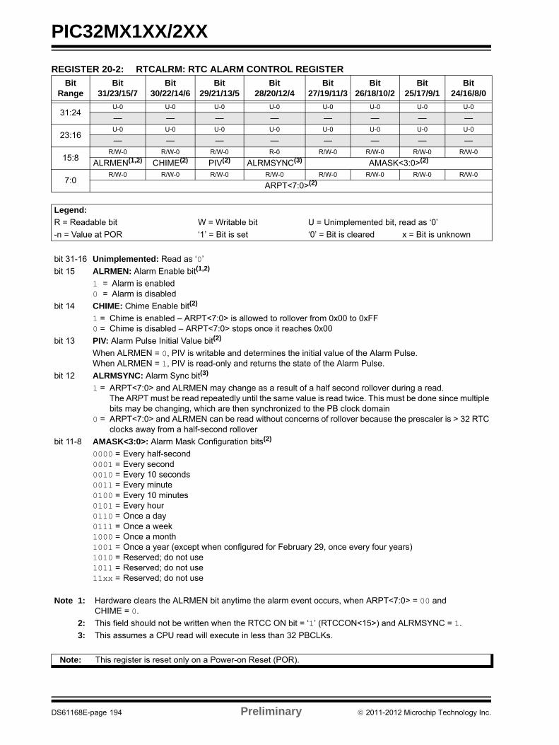
PIC32MX1XX/2XX
REGISTER 20-2: RTCALRM: RTC ALARM CONTROL REGISTER
Bit Range
Bit31/23/15/7
Bit30/22/14/6
Bit29/21/13/5
Bit28/20/12/4
Bit27/19/11/3
Bit26/18/10/2
Bit25/17/9/1
Bit24/16/8/0
31:24U-0 U-0 U-0 U-0 U-0 U-0 U-0 U-0
— — — — — — — —
23:16U-0 U-0 U-0 U-0 U-0 U-0 U-0 U-0
— — — — — — — —
15:8R/W-0 R/W-0 R/W-0 R-0 R/W-0 R/W-0 R/W-0 R/W-0
ALRMEN(1,2) CHIME(2) PIV(2) ALRMSYNC(3) AMASK<3:0>(2)
7:0R/W-0 R/W-0 R/W-0 R/W-0 R/W-0 R/W-0 R/W-0 R/W-0
ARPT<7:0>(2)
Legend:
R = Readable bit W = Writable bit U = Unimplemented bit, read as ‘0’
-n = Value at POR ‘1’ = Bit is set ‘0’ = Bit is cleared x = Bit is unknown
bit 31-16 Unimplemented: Read as ‘0’
bit 15 ALRMEN: Alarm Enable bit(1,2)
1 = Alarm is enabled0 = Alarm is disabled
bit 14 CHIME: Chime Enable bit(2)
1 = Chime is enabled – ARPT<7:0> is allowed to rollover from 0x00 to 0xFF0 = Chime is disabled – ARPT<7:0> stops once it reaches 0x00
bit 13 PIV: Alarm Pulse Initial Value bit(2)
When ALRMEN = 0, PIV is writable and determines the initial value of the Alarm Pulse.When ALRMEN = 1, PIV is read-only and returns the state of the Alarm Pulse.
bit 12 ALRMSYNC: Alarm Sync bit(3)
1 = ARPT<7:0> and ALRMEN may change as a result of a half second rollover during a read. The ARPT must be read repeatedly until the same value is read twice. This must be done since multiplebits may be changing, which are then synchronized to the PB clock domain
0 = ARPT<7:0> and ALRMEN can be read without concerns of rollover because the prescaler is > 32 RTCclocks away from a half-second rollover
bit 11-8 AMASK<3:0>: Alarm Mask Configuration bits(2)
0000 = Every half-second0001 = Every second0010 = Every 10 seconds0011 = Every minute0100 = Every 10 minutes0101 = Every hour0110 = Once a day0111 = Once a week1000 = Once a month1001 = Once a year (except when configured for February 29, once every four years)1010 = Reserved; do not use1011 = Reserved; do not use11xx = Reserved; do not use
Note 1: Hardware clears the ALRMEN bit anytime the alarm event occurs, when ARPT<7:0> = 00 and CHIME = 0.
2: This field should not be written when the RTCC ON bit = ‘1’ (RTCCON<15>) and ALRMSYNC = 1.
3: This assumes a CPU read will execute in less than 32 PBCLKs.
Note: This register is reset only on a Power-on Reset (POR).
DS61168E-page 194 Preliminary 2011-2012 Microchip Technology Inc.
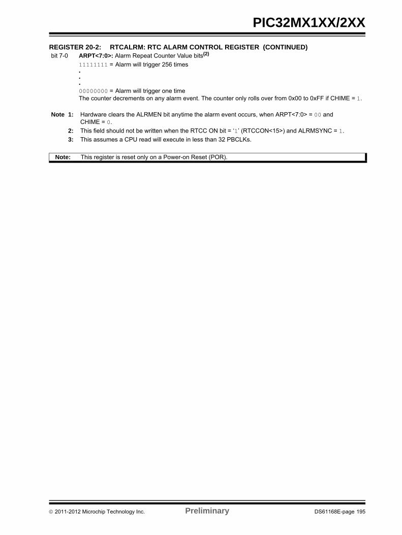
PIC32MX1XX/2XX
bit 7-0 ARPT<7:0>: Alarm Repeat Counter Value bits(2)
11111111 = Alarm will trigger 256 times•••
00000000 = Alarm will trigger one timeThe counter decrements on any alarm event. The counter only rolls over from 0x00 to 0xFF if CHIME = 1.
REGISTER 20-2: RTCALRM: RTC ALARM CONTROL REGISTER (CONTINUED)
Note 1: Hardware clears the ALRMEN bit anytime the alarm event occurs, when ARPT<7:0> = 00 and CHIME = 0.
2: This field should not be written when the RTCC ON bit = ‘1’ (RTCCON<15>) and ALRMSYNC = 1.
3: This assumes a CPU read will execute in less than 32 PBCLKs.
Note: This register is reset only on a Power-on Reset (POR).
2011-2012 Microchip Technology Inc. Preliminary DS61168E-page 195
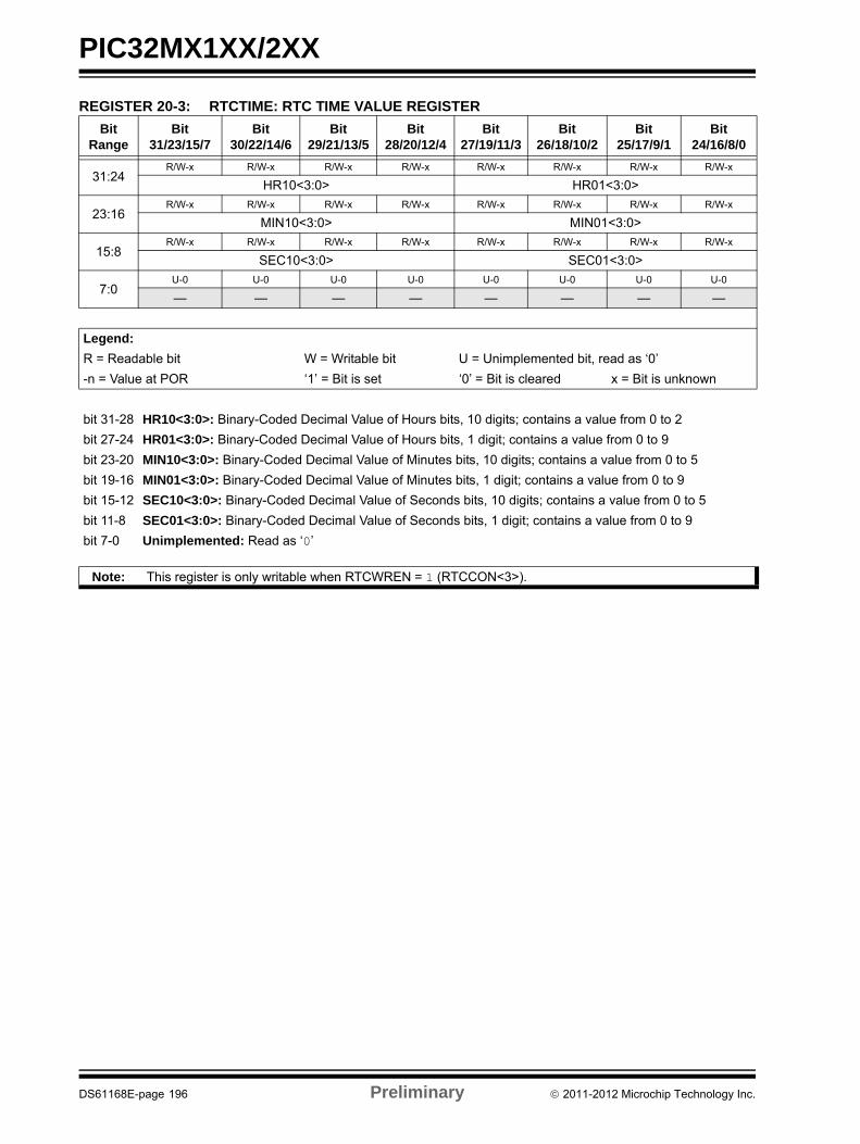
PIC32MX1XX/2XX
REGISTER 20-3: RTCTIME: RTC TIME VALUE REGISTER
Bit Range
Bit31/23/15/7
Bit30/22/14/6
Bit29/21/13/5
Bit28/20/12/4
Bit27/19/11/3
Bit26/18/10/2
Bit25/17/9/1
Bit24/16/8/0
31:24R/W-x R/W-x R/W-x R/W-x R/W-x R/W-x R/W-x R/W-x
HR10<3:0> HR01<3:0>
23:16R/W-x R/W-x R/W-x R/W-x R/W-x R/W-x R/W-x R/W-x
MIN10<3:0> MIN01<3:0>
15:8R/W-x R/W-x R/W-x R/W-x R/W-x R/W-x R/W-x R/W-x
SEC10<3:0> SEC01<3:0>
7:0U-0 U-0 U-0 U-0 U-0 U-0 U-0 U-0
— — — — — — — —
Legend:
R = Readable bit W = Writable bit U = Unimplemented bit, read as ‘0’
-n = Value at POR ‘1’ = Bit is set ‘0’ = Bit is cleared x = Bit is unknown
bit 31-28 HR10<3:0>: Binary-Coded Decimal Value of Hours bits, 10 digits; contains a value from 0 to 2
bit 27-24 HR01<3:0>: Binary-Coded Decimal Value of Hours bits, 1 digit; contains a value from 0 to 9
bit 23-20 MIN10<3:0>: Binary-Coded Decimal Value of Minutes bits, 10 digits; contains a value from 0 to 5
bit 19-16 MIN01<3:0>: Binary-Coded Decimal Value of Minutes bits, 1 digit; contains a value from 0 to 9
bit 15-12 SEC10<3:0>: Binary-Coded Decimal Value of Seconds bits, 10 digits; contains a value from 0 to 5
bit 11-8 SEC01<3:0>: Binary-Coded Decimal Value of Seconds bits, 1 digit; contains a value from 0 to 9
bit 7-0 Unimplemented: Read as ‘0’
Note: This register is only writable when RTCWREN = 1 (RTCCON<3>).
DS61168E-page 196 Preliminary 2011-2012 Microchip Technology Inc.
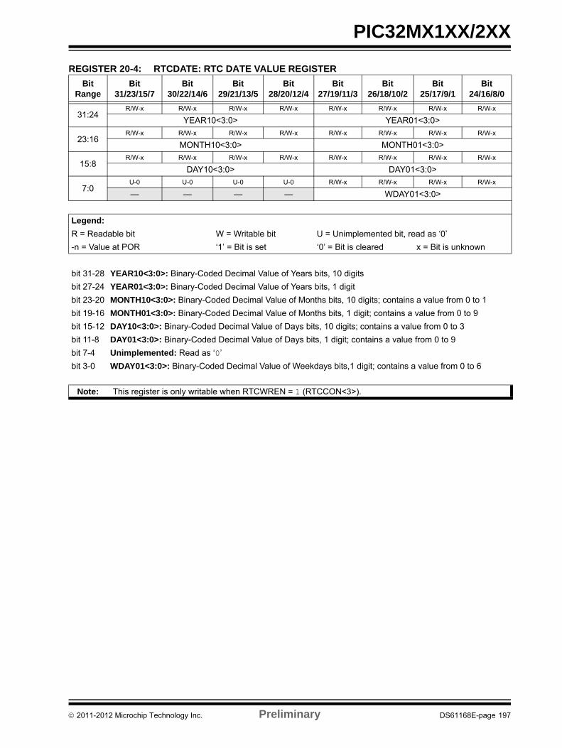
PIC32MX1XX/2XX
REGISTER 20-4: RTCDATE: RTC DATE VALUE REGISTER
Bit Range
Bit31/23/15/7
Bit30/22/14/6
Bit29/21/13/5
Bit28/20/12/4
Bit27/19/11/3
Bit26/18/10/2
Bit25/17/9/1
Bit24/16/8/0
31:24R/W-x R/W-x R/W-x R/W-x R/W-x R/W-x R/W-x R/W-x
YEAR10<3:0> YEAR01<3:0>
23:16R/W-x R/W-x R/W-x R/W-x R/W-x R/W-x R/W-x R/W-x
MONTH10<3:0> MONTH01<3:0>
15:8R/W-x R/W-x R/W-x R/W-x R/W-x R/W-x R/W-x R/W-x
DAY10<3:0> DAY01<3:0>
7:0U-0 U-0 U-0 U-0 R/W-x R/W-x R/W-x R/W-x
— — — — WDAY01<3:0>
Legend:
R = Readable bit W = Writable bit U = Unimplemented bit, read as ‘0’
-n = Value at POR ‘1’ = Bit is set ‘0’ = Bit is cleared x = Bit is unknown
bit 31-28 YEAR10<3:0>: Binary-Coded Decimal Value of Years bits, 10 digits
bit 27-24 YEAR01<3:0>: Binary-Coded Decimal Value of Years bits, 1 digit
bit 23-20 MONTH10<3:0>: Binary-Coded Decimal Value of Months bits, 10 digits; contains a value from 0 to 1
bit 19-16 MONTH01<3:0>: Binary-Coded Decimal Value of Months bits, 1 digit; contains a value from 0 to 9
bit 15-12 DAY10<3:0>: Binary-Coded Decimal Value of Days bits, 10 digits; contains a value from 0 to 3
bit 11-8 DAY01<3:0>: Binary-Coded Decimal Value of Days bits, 1 digit; contains a value from 0 to 9
bit 7-4 Unimplemented: Read as ‘0’
bit 3-0 WDAY01<3:0>: Binary-Coded Decimal Value of Weekdays bits,1 digit; contains a value from 0 to 6
Note: This register is only writable when RTCWREN = 1 (RTCCON<3>).
2011-2012 Microchip Technology Inc. Preliminary DS61168E-page 197
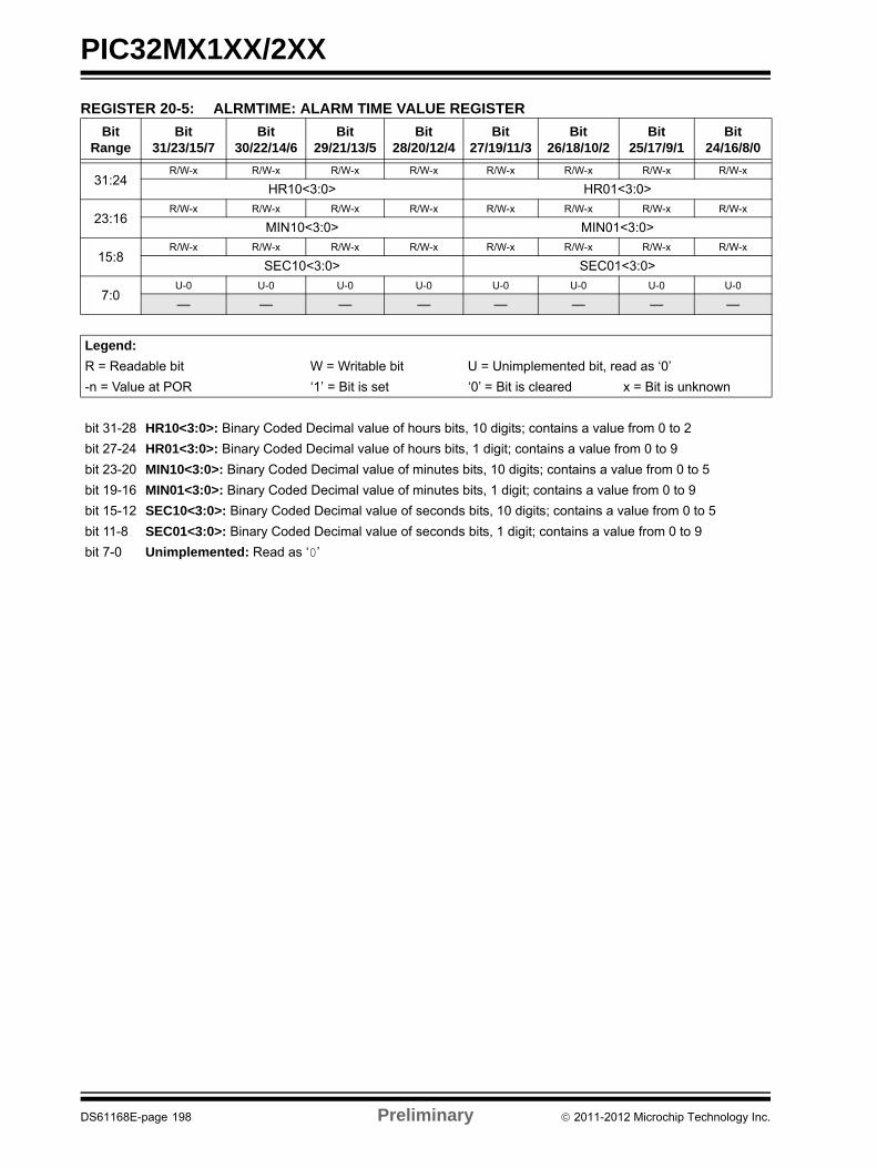
PIC32MX1XX/2XX
REGISTER 20-5: ALRMTIME: ALARM TIME VALUE REGISTER
Bit Range
Bit31/23/15/7
Bit30/22/14/6
Bit29/21/13/5
Bit28/20/12/4
Bit27/19/11/3
Bit26/18/10/2
Bit25/17/9/1
Bit24/16/8/0
31:24R/W-x R/W-x R/W-x R/W-x R/W-x R/W-x R/W-x R/W-x
HR10<3:0> HR01<3:0>
23:16R/W-x R/W-x R/W-x R/W-x R/W-x R/W-x R/W-x R/W-x
MIN10<3:0> MIN01<3:0>
15:8R/W-x R/W-x R/W-x R/W-x R/W-x R/W-x R/W-x R/W-x
SEC10<3:0> SEC01<3:0>
7:0U-0 U-0 U-0 U-0 U-0 U-0 U-0 U-0
— — — — — — — —
Legend:
R = Readable bit W = Writable bit U = Unimplemented bit, read as ‘0’
-n = Value at POR ‘1’ = Bit is set ‘0’ = Bit is cleared x = Bit is unknown
bit 31-28 HR10<3:0>: Binary Coded Decimal value of hours bits, 10 digits; contains a value from 0 to 2
bit 27-24 HR01<3:0>: Binary Coded Decimal value of hours bits, 1 digit; contains a value from 0 to 9
bit 23-20 MIN10<3:0>: Binary Coded Decimal value of minutes bits, 10 digits; contains a value from 0 to 5
bit 19-16 MIN01<3:0>: Binary Coded Decimal value of minutes bits, 1 digit; contains a value from 0 to 9
bit 15-12 SEC10<3:0>: Binary Coded Decimal value of seconds bits, 10 digits; contains a value from 0 to 5
bit 11-8 SEC01<3:0>: Binary Coded Decimal value of seconds bits, 1 digit; contains a value from 0 to 9
bit 7-0 Unimplemented: Read as ‘0’
DS61168E-page 198 Preliminary 2011-2012 Microchip Technology Inc.
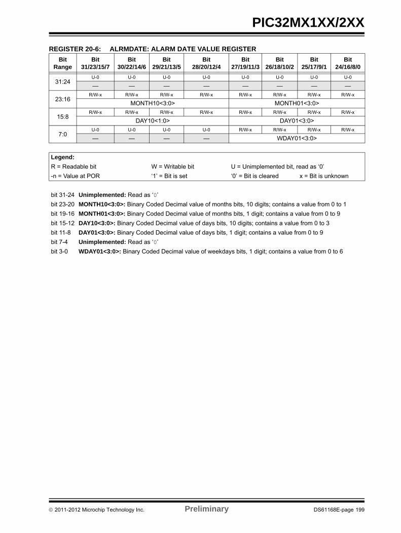
PIC32MX1XX/2XX
REGISTER 20-6: ALRMDATE: ALARM DATE VALUE REGISTER
Bit Range
Bit31/23/15/7
Bit30/22/14/6
Bit29/21/13/5
Bit28/20/12/4
Bit27/19/11/3
Bit26/18/10/2
Bit25/17/9/1
Bit24/16/8/0
31:24U-0 U-0 U-0 U-0 U-0 U-0 U-0 U-0
— — — — — — — —
23:16R/W-x R/W-x R/W-x R/W-x R/W-x R/W-x R/W-x R/W-x
MONTH10<3:0> MONTH01<3:0>
15:8R/W-x R/W-x R/W-x R/W-x R/W-x R/W-x R/W-x R/W-x
DAY10<1:0> DAY01<3:0>
7:0U-0 U-0 U-0 U-0 R/W-x R/W-x R/W-x R/W-x
— — — — WDAY01<3:0>
Legend:
R = Readable bit W = Writable bit U = Unimplemented bit, read as ‘0’
-n = Value at POR ‘1’ = Bit is set ‘0’ = Bit is cleared x = Bit is unknown
bit 31-24 Unimplemented: Read as ‘0’
bit 23-20 MONTH10<3:0>: Binary Coded Decimal value of months bits, 10 digits; contains a value from 0 to 1
bit 19-16 MONTH01<3:0>: Binary Coded Decimal value of months bits, 1 digit; contains a value from 0 to 9
bit 15-12 DAY10<3:0>: Binary Coded Decimal value of days bits, 10 digits; contains a value from 0 to 3
bit 11-8 DAY01<3:0>: Binary Coded Decimal value of days bits, 1 digit; contains a value from 0 to 9
bit 7-4 Unimplemented: Read as ‘0’
bit 3-0 WDAY01<3:0>: Binary Coded Decimal value of weekdays bits, 1 digit; contains a value from 0 to 6
2011-2012 Microchip Technology Inc. Preliminary DS61168E-page 199

PIC32MX1XX/2XX
NOTES:
DS61168E-page 200 Preliminary 2011-2012 Microchip Technology Inc.
PIC32MX1XX/2XX
21.0 10-BIT ANALOG-TO-DIGITAL CONVERTER (ADC)
The PIC32MX1XX/2XX 10-bit Analog-to-DigitalConverter (ADC) includes the following features:
• Successive Approximation Register (SAR) conversion
• Up to 1 Msps conversion speed• Up to 13 analog input pins• External voltage reference input pins• One unipolar, differential Sample and Hold
Amplifier (SHA)
• Automatic Channel Scan mode• Selectable conversion trigger source• 16-word conversion result buffer• Selectable buffer fill modes• Eight conversion result format options • Operation during CPU Sleep and Idle modes
A block diagram of the 10-bit ADC is illustrated inFigure 21-1. The 10-bit ADC has up to 13 analog inputpins, designated AN0-AN12. In addition, there are twoanalog input pins for external voltage referenceconnections. These voltage reference inputs may beshared with other analog input pins and may becommon to other analog module references.
FIGURE 21-1: ADC1 MODULE BLOCK DIAGRAM
Note 1: This data sheet summarizes the featuresof the PIC32MX1XX/2XX family ofdevices. It is not intended to be acomprehensive reference source. Tocomplement the information in this datasheet, refer to Section 17. “10-bitAnalog-to-Digital Converter (ADC)”(DS61104) in the “PIC32 FamilyReference Manual”, which is availablefrom the Microchip web site(www.microchip.com/PIC32).
2: Some registers and associated bitsdescribed in this section may not beavailable on all devices. Refer toSection 4.0 “Memory Organization” inthis data sheet for device-specific registerand bit information.
SAR ADC
S&H
ADC1BUF0
ADC1BUF1
ADC1BUF2
ADC1BUFF
ADC1BUFE
CTMUT(3)
IVREF(4)
AN1
VREFL
CH0SB<4:0>
CH0NA CH0NB
+
-CH0SA<4:0>
ChannelScan
CSCNA
Alternate
VREF+(1) AVDD AVSSVREF-(1)
Note 1: VREF+ and VREF- inputs can be multiplexed with other analog inputs.
2: AN8 is only available on 44-pin devices. AN6 and AN7 are not available on 28-pin devices.
3: Connected to the CTMU module. See Section 24.0 “Charge Time Measurement Unit (CTMU)” for moreinformation.
4: See Section 23.0 “Comparator Voltage Reference (CVREF)” for more information.
5: This selection is only used with CTMU capacitive and time measurement.
Input Selection
VREFH VREFL
VCFG<2:0>AN12(2)
AN0
Open(5)
CTMUI(3)
2011-2012 Microchip Technology Inc. Preliminary DS61168E-page 201
PIC32MX1XX/2XX
FIGURE 21-2: ADC CONVERSION CLOCK PERIOD BLOCK DIAGRAM
1
0
Div 2
TPB(2)
ADC ConversionClock Multiplier
2, 4,..., 512
ADRC
TAD
8
ADCS<7:0>
FRC(1)
Note 1: See Section 29.0 “Electrical Characteristics” for the exact FRC clock value.
2: Refer to Figure 8-1 in Section 8.0 “Oscillator Configuration” for more information.
DS61168E-page 202 Preliminary 2011-2012 Microchip Technology Inc.
PIC32MX1XX/2XX
REGISTER 21-1: AD1CON1: ADC CONTROL REGISTER 1
Bit Range
Bit31/23/15/7
Bit30/22/14/6
Bit29/21/13/5
Bit28/20/12/4
Bit27/19/11/3
Bit26/18/10/2
Bit25/17/9/1
Bit24/16/8/0
31:24U-0 U-0 U-0 U-0 U-0 U-0 U-0 U-0
— — — — — — — —
23:16U-0 U-0 U-0 U-0 U-0 U-0 U-0 U-0
— — — — — — — —
15:8R/W-0 U-0 R/W-0 U-0 U-0 R/W-0 R/W-0 R/W-0
ON(1) — SIDL — — FORM<2:0>
7:0R/W-0 R/W-0 R/W-0 R/W-0 U-0 R/W-0 R/W-0, HSC R/C-0, HSC
SSRC<2:0> CLRASAM — ASAM SAMP(2) DONE(3)
Legend:
R = Readable bit W = Writable bit U = Unimplemented bit, read as ‘0’
-n = Value at POR ‘1’ = Bit is set ‘0’ = Bit is cleared x = Bit is unknown
bit 31-16 Unimplemented: Read as ‘0’
bit 15 ON: ADC Operating Mode bit(1)
1 = ADC module is operating0 = ADC module is not operating
bit 14 Unimplemented: Read as ‘0’
bit 13 SIDL: Stop in Idle Mode bit
1 = Discontinue module operation when device enters Idle mode0 = Continue module operation in Idle mode
bit 12-11 Unimplemented: Read as ‘0’
bit 10-8 FORM<2:0>: Data Output Format bits
111 = Signed Fractional 32-bit (DOUT = sddd dddd dd00 0000 0000 0000 0000)110 = Fractional 32-bit (DOUT = dddd dddd dd00 0000 0000 0000 0000 0000)101 = Signed Integer 32-bit (DOUT = ssss ssss ssss ssss ssss sssd dddd dddd)100 = Integer 32-bit (DOUT = 0000 0000 0000 0000 0000 00dd dddd dddd)011 = Signed Fractional 16-bit (DOUT = 0000 0000 0000 0000 sddd dddd dd00 0000)010 = Fractional 16-bit (DOUT = 0000 0000 0000 0000 dddd dddd dd00 0000)001 = Signed Integer 16-bit (DOUT = 0000 0000 0000 0000 ssss sssd dddd dddd)000 =Integer 16-bit (DOUT = 0000 0000 0000 0000 0000 00dd dddd dddd)
bit 7-5 SSRC<2:0>: Conversion Trigger Source Select bits
111 = Internal counter ends sampling and starts conversion (auto convert)110 = Reserved101 = Reserved100 = Reserved011 = CTMU ends sampling and starts conversion010 = Timer 3 period match ends sampling and starts conversion001 = Active transition on INT0 pin ends sampling and starts conversion000 = Clearing SAMP bit ends sampling and starts conversion
Note 1: When using 1:1 PBCLK divisor, the user’s software should not read/write the peripheral’s SFRs in the SYSCLK cycle immediately following the instruction that clears the module’s ON bit.
2: If ASAM = 0, software can write a ‘1’ to start sampling. This bit is automatically set by hardware if ASAM = 1. If SSRC = 0, software can write a ‘0’ to end sampling and start conversion. If SSRC ‘0’, this bit is automatically cleared by hardware to end sampling and start conversion.
3: This bit is automatically set by hardware when analog-to-digital conversion is complete. Software can write a ‘0’ to clear this bit (a write of ‘1’ is not allowed). Clearing this bit does not affect any operation already in progress. This bit is automatically cleared by hardware at the start of a new conversion.
2011-2012 Microchip Technology Inc. Preliminary DS61168E-page 203
PIC32MX1XX/2XX
bit 4 CLRASAM: Stop Conversion Sequence bit (when the first ADC interrupt is generated)1 = Stop conversions when the first ADC interrupt is generated. Hardware clears the ASAM bit when the
ADC interrupt is generated.0 = Normal operation, buffer contents will be overwritten by the next conversion sequence
bit 3 Unimplemented: Read as ‘0’
bit 2 ASAM: ADC Sample Auto-Start bit
1 = Sampling begins immediately after last conversion completes; SAMP bit is automatically set.0 = Sampling begins when SAMP bit is set
bit 1 SAMP: ADC Sample Enable bit(2)
1 = The ADC sample and hold amplifier is sampling0 = The ADC sample/hold amplifier is holdingWhen ASAM = 0, writing ‘1’ to this bit starts sampling. When SSRC = 000, writing ‘0’ to this bit will end sampling and start conversion.
bit 0 DONE: Analog-to-Digital Conversion Status bit(3)
1 = Analog-to-digital conversion is done0 = Analog-to-digital conversion is not done or has not startedClearing this bit will not affect any operation in progress.
REGISTER 21-1: AD1CON1: ADC CONTROL REGISTER 1 (CONTINUED)
Note 1: When using 1:1 PBCLK divisor, the user’s software should not read/write the peripheral’s SFRs in the SYSCLK cycle immediately following the instruction that clears the module’s ON bit.
2: If ASAM = 0, software can write a ‘1’ to start sampling. This bit is automatically set by hardware if ASAM = 1. If SSRC = 0, software can write a ‘0’ to end sampling and start conversion. If SSRC ‘0’, this bit is automatically cleared by hardware to end sampling and start conversion.
3: This bit is automatically set by hardware when analog-to-digital conversion is complete. Software can write a ‘0’ to clear this bit (a write of ‘1’ is not allowed). Clearing this bit does not affect any operation already in progress. This bit is automatically cleared by hardware at the start of a new conversion.
DS61168E-page 204 Preliminary 2011-2012 Microchip Technology Inc.
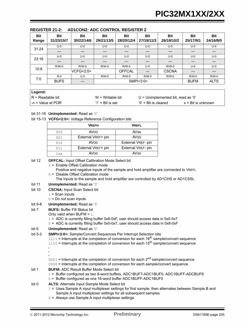
PIC32MX1XX/2XX
REGISTER 21-2: AD1CON2: ADC CONTROL REGISTER 2
Bit Range
Bit31/23/15/7
Bit30/22/14/6
Bit29/21/13/5
Bit28/20/12/4
Bit27/19/11/3
Bit26/18/10/2
Bit25/17/9/1
Bit24/16/8/0
31:24U-0 U-0 U-0 U-0 U-0 U-0 U-0 U-0
— — — — — — — —
23:16U-0 U-0 U-0 U-0 U-0 U-0 U-0 U-0
— — — — — — — —
15:8R/W-0 R/W-0 R/W-0 R/W-0 U-0 R/W-0 U-0 U-0
VCFG<2:0> OFFCAL — CSCNA — —
7:0R-0 U-0 R/W-0 R/W-0 R/W-0 R/W-0 R/W-0 R/W-0
BUFS — SMPI<3:0> BUFM ALTS
Legend:
R = Readable bit W = Writable bit U = Unimplemented bit, read as ‘0’
-n = Value at POR ‘1’ = Bit is set ‘0’ = Bit is cleared x = Bit is unknown
bit 31-16 Unimplemented: Read as ‘0’
bit 15-13 VCFG<2:0>: Voltage Reference Configuration bits
VREFH VREFL
000 AVDD AVss
001 External VREF+ pin AVSS
010 AVDD External VREF- pin
011 External VREF+ pin External VREF- pin
1xx AVDD AVSS
bit 12 OFFCAL: Input Offset Calibration Mode Select bit1 = Enable Offset Calibration mode
Positive and negative inputs of the sample and hold amplifier are connected to VREFL
0 = Disable Offset Calibration modeThe inputs to the sample and hold amplifier are controlled by AD1CHS or AD1CSSL
bit 11 Unimplemented: Read as ‘0’
bit 10 CSCNA: Input Scan Select bit1 = Scan inputs0 = Do not scan inputs
bit 9-8 Unimplemented: Read as ‘0’
bit 7 BUFS: Buffer Fill Status bitOnly valid when BUFM = 1.1 = ADC is currently filling buffer 0x8-0xF, user should access data in 0x0-0x70 = ADC is currently filling buffer 0x0-0x7, user should access data in 0x8-0xF
bit 6 Unimplemented: Read as ‘0’
bit 5-2 SMPI<3:0>: Sample/Convert Sequences Per Interrupt Selection bits1111 = Interrupts at the completion of conversion for each 16th sample/convert sequence1110 = Interrupts at the completion of conversion for each 15th sample/convert sequence•••
0001 = Interrupts at the completion of conversion for each 2nd sample/convert sequence0000 = Interrupts at the completion of conversion for each sample/convert sequence
bit 1 BUFM: ADC Result Buffer Mode Select bit1 = Buffer configured as two 8-word buffers, ADC1BUF7-ADC1BUF0, ADC1BUFF-ADCBUF80 = Buffer configured as one 16-word buffer ADC1BUFF-ADC1BUF0
bit 0 ALTS: Alternate Input Sample Mode Select bit1 = Uses Sample A input multiplexer settings for first sample, then alternates between Sample B and
Sample A input multiplexer settings for all subsequent samples0 = Always use Sample A input multiplexer settings
2011-2012 Microchip Technology Inc. Preliminary DS61168E-page 205
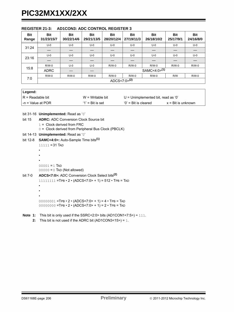
PIC32MX1XX/2XX
REGISTER 21-3: AD1CON3: ADC CONTROL REGISTER 3
Bit Range
Bit31/23/15/7
Bit30/22/14/6
Bit29/21/13/5
Bit28/20/12/4
Bit27/19/11/3
Bit26/18/10/2
Bit25/17/9/1
Bit24/16/8/0
31:24U-0 U-0 U-0 U-0 U-0 U-0 U-0 U-0
— — — — — — — —
23:16U-0 U-0 U-0 U-0 U-0 U-0 U-0 U-0
— — — — — — — —
15:8R/W-0 U-0 U-0 R/W-0 R/W-0 R/W-0 R/W-0 R/W-0
ADRC — — SAMC<4:0>(1)
7:0R/W-0 R/W-0 R/W-0 R/W-0 R/W-0 R/W-0 R/W R/W-0
ADCS<7:0>(2)
Legend:
R = Readable bit W = Writable bit U = Unimplemented bit, read as ‘0’
-n = Value at POR ‘1’ = Bit is set ‘0’ = Bit is cleared x = Bit is unknown
bit 31-16 Unimplemented: Read as ‘0’
bit 15 ADRC: ADC Conversion Clock Source bit
1 = Clock derived from FRC0 = Clock derived from Peripheral Bus Clock (PBCLK)
bit 14-13 Unimplemented: Read as ‘0’
bit 12-8 SAMC<4:0>: Auto-Sample Time bits(1)
11111 = 31 TAD
•
•
•
00001 =1 TAD
00000 =0 TAD (Not allowed)
bit 7-0 ADCS<7:0>: ADC Conversion Clock Select bits(2)
11111111 =TPB • 2 • (ADCS<7:0> + 1) = 512 • TPB = TAD
•
•
•
00000001 =TPB • 2 • (ADCS<7:0> + 1) = 4 • TPB = TAD
00000000 =TPB • 2 • (ADCS<7:0> + 1) = 2 • TPB = TAD
Note 1: This bit is only used if the SSRC<2:0> bits (AD1CON1<7:5>) = 111.
2: This bit is not used if the ADRC bit (AD1CON3<15>) = 1.
DS61168E-page 206 Preliminary 2011-2012 Microchip Technology Inc.
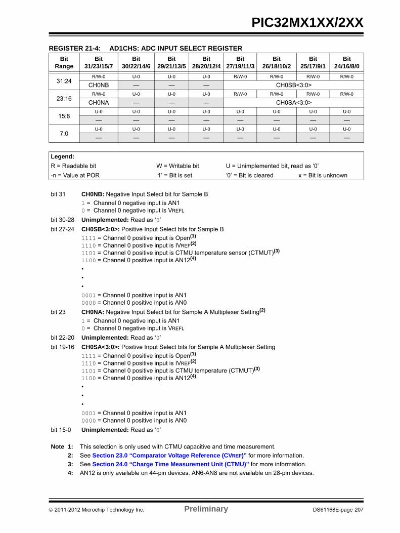
PIC32MX1XX/2XX
REGISTER 21-4: AD1CHS: ADC INPUT SELECT REGISTER
Bit Range
Bit31/23/15/7
Bit30/22/14/6
Bit29/21/13/5
Bit28/20/12/4
Bit27/19/11/3
Bit26/18/10/2
Bit25/17/9/1
Bit24/16/8/0
31:24R/W-0 U-0 U-0 U-0 R/W-0 R/W-0 R/W-0 R/W-0
CH0NB — — — CH0SB<3:0>
23:16R/W-0 U-0 U-0 U-0 R/W-0 R/W-0 R/W-0 R/W-0
CH0NA — — — CH0SA<3:0>
15:8U-0 U-0 U-0 U-0 U-0 U-0 U-0 U-0
— — — — — — — —
7:0U-0 U-0 U-0 U-0 U-0 U-0 U-0 U-0
— — — — — — — —
Legend:
R = Readable bit W = Writable bit U = Unimplemented bit, read as ‘0’
-n = Value at POR ‘1’ = Bit is set ‘0’ = Bit is cleared x = Bit is unknown
bit 31 CH0NB: Negative Input Select bit for Sample B
1 = Channel 0 negative input is AN10 = Channel 0 negative input is VREFL
bit 30-28 Unimplemented: Read as ‘0’
bit 27-24 CH0SB<3:0>: Positive Input Select bits for Sample B
1111 = Channel 0 positive input is Open(1)
1110 = Channel 0 positive input is IVREF(2)
1101 = Channel 0 positive input is CTMU temperature sensor (CTMUT)(3)
1100 = Channel 0 positive input is AN12(4)
•
•
•
0001 = Channel 0 positive input is AN10000 = Channel 0 positive input is AN0
bit 23 CH0NA: Negative Input Select bit for Sample A Multiplexer Setting(2)
1 = Channel 0 negative input is AN10 = Channel 0 negative input is VREFL
bit 22-20 Unimplemented: Read as ‘0’
bit 19-16 CH0SA<3:0>: Positive Input Select bits for Sample A Multiplexer Setting
1111 = Channel 0 positive input is Open(1)
1110 = Channel 0 positive input is IVREF(2)
1101 = Channel 0 positive input is CTMU temperature (CTMUT)(3)
1100 = Channel 0 positive input is AN12(4)
•
•
•
0001 = Channel 0 positive input is AN10000 = Channel 0 positive input is AN0
bit 15-0 Unimplemented: Read as ‘0’
Note 1: This selection is only used with CTMU capacitive and time measurement.
2: See Section 23.0 “Comparator Voltage Reference (CVREF)” for more information.
3: See Section 24.0 “Charge Time Measurement Unit (CTMU)” for more information.
4: AN12 is only available on 44-pin devices. AN6-AN8 are not available on 28-pin devices.
2011-2012 Microchip Technology Inc. Preliminary DS61168E-page 207
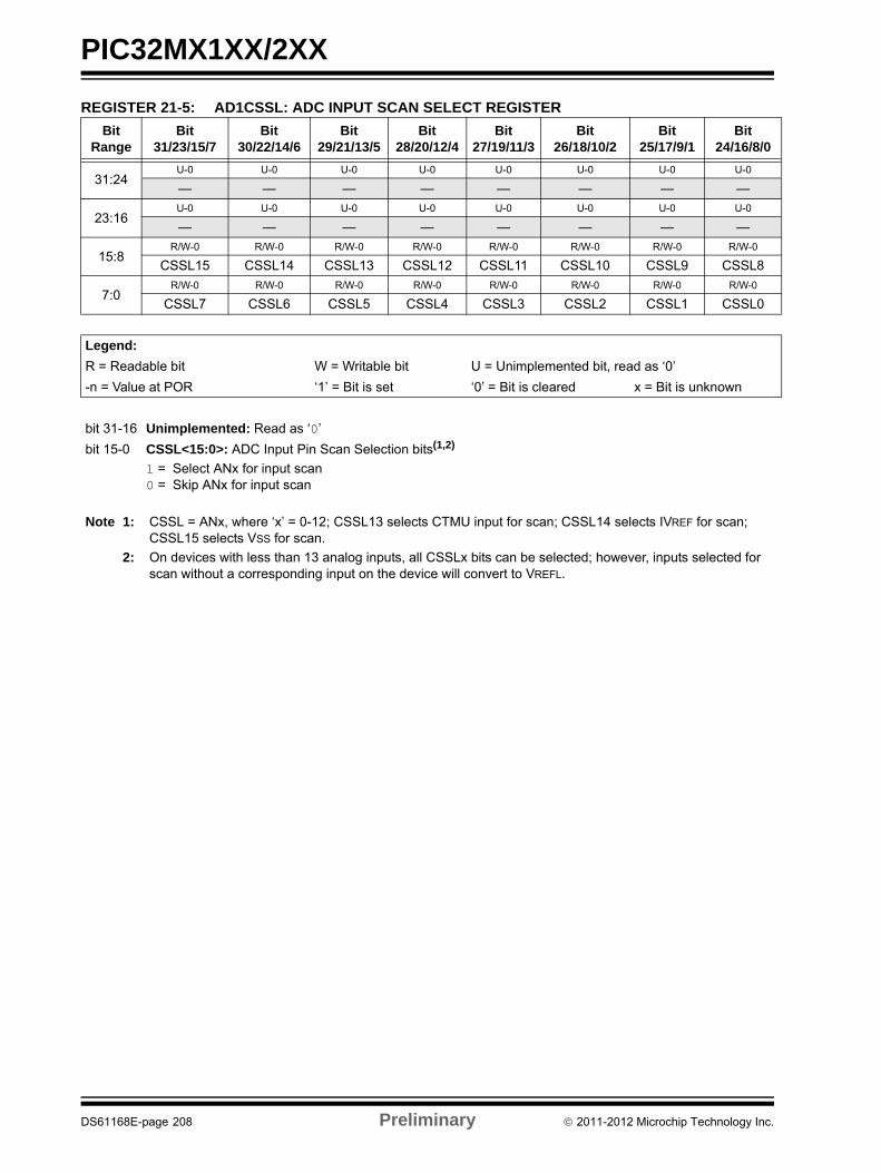
PIC32MX1XX/2XX
REGISTER 21-5: AD1CSSL: ADC INPUT SCAN SELECT REGISTER
Bit Range
Bit31/23/15/7
Bit30/22/14/6
Bit29/21/13/5
Bit28/20/12/4
Bit27/19/11/3
Bit26/18/10/2
Bit25/17/9/1
Bit24/16/8/0
31:24U-0 U-0 U-0 U-0 U-0 U-0 U-0 U-0
— — — — — — — —
23:16U-0 U-0 U-0 U-0 U-0 U-0 U-0 U-0
— — — — — — — —
15:8R/W-0 R/W-0 R/W-0 R/W-0 R/W-0 R/W-0 R/W-0 R/W-0
CSSL15 CSSL14 CSSL13 CSSL12 CSSL11 CSSL10 CSSL9 CSSL8
7:0R/W-0 R/W-0 R/W-0 R/W-0 R/W-0 R/W-0 R/W-0 R/W-0
CSSL7 CSSL6 CSSL5 CSSL4 CSSL3 CSSL2 CSSL1 CSSL0
Legend:
R = Readable bit W = Writable bit U = Unimplemented bit, read as ‘0’
-n = Value at POR ‘1’ = Bit is set ‘0’ = Bit is cleared x = Bit is unknown
bit 31-16 Unimplemented: Read as ‘0’
bit 15-0 CSSL<15:0>: ADC Input Pin Scan Selection bits(1,2)
1 = Select ANx for input scan0 = Skip ANx for input scan
Note 1: CSSL = ANx, where ‘x’ = 0-12; CSSL13 selects CTMU input for scan; CSSL14 selects IVREF for scan; CSSL15 selects VSS for scan.
2: On devices with less than 13 analog inputs, all CSSLx bits can be selected; however, inputs selected for scan without a corresponding input on the device will convert to VREFL.
DS61168E-page 208 Preliminary 2011-2012 Microchip Technology Inc.
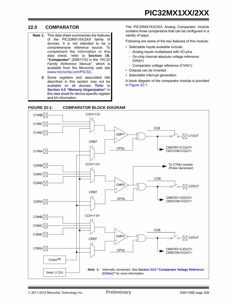
PIC32MX1XX/2XX
22.0 COMPARATOR The PIC32MX1XX/2XX Analog Comparator modulecontains three comparators that can be configured in avariety of ways.
Following are some of the key features of this module:
• Selectable inputs available include:- Analog inputs multiplexed with I/O pins- On-chip internal absolute voltage reference
(IVREF)- Comparator voltage reference (CVREF)
• Outputs can be Inverted• Selectable interrupt generation
A block diagram of the comparator module is providedin Figure 22-1.
FIGURE 22-1: COMPARATOR BLOCK DIAGRAM
Note 1: This data sheet summarizes the featuresof the PIC32MX1XX/2XX family ofdevices. It is not intended to be acomprehensive reference source. Tocomplement the information in thisdata sheet, refer to Section 19.“Comparator” (DS61110) in the “PIC32Family Reference Manual”, which isavailable from the Microchip web site(www.microchip.com/PIC32).
2: Some registers and associated bitsdescribed in this section may not beavailable on all devices. Refer toSection 4.0 “Memory Organization” inthis data sheet for device-specific registerand bit information.
C3IND
C3INA
C3OUTCMP3
COE
CREF
CCH<1:0>
CPOL
C3INC
C3INB
CVREF(1)
IVREF (1.2V)
C2IND
C2INA
C2OUTCMP2
COE
CREF
CCH<1:0>
CPOL
C2INC
C2INB
C1IND
C1INA
C1OUTCMP1
COE
CREF
CCH<1:0>
CPOL
C1INC
C1INB
CMSTAT<C1OUT>CM1CON<COUT>
CMSTAT<C2OUT>CM2CON<COUT>
CMSTAT<C3OUT>CM3CON<COUT>
To CTMU module(Pulse Generator)
Note 1: Internally connected. See Section 23.0 “Comparator Voltage Reference(CVREF)” for more information.
2011-2012 Microchip Technology Inc. Preliminary DS61168E-page 209
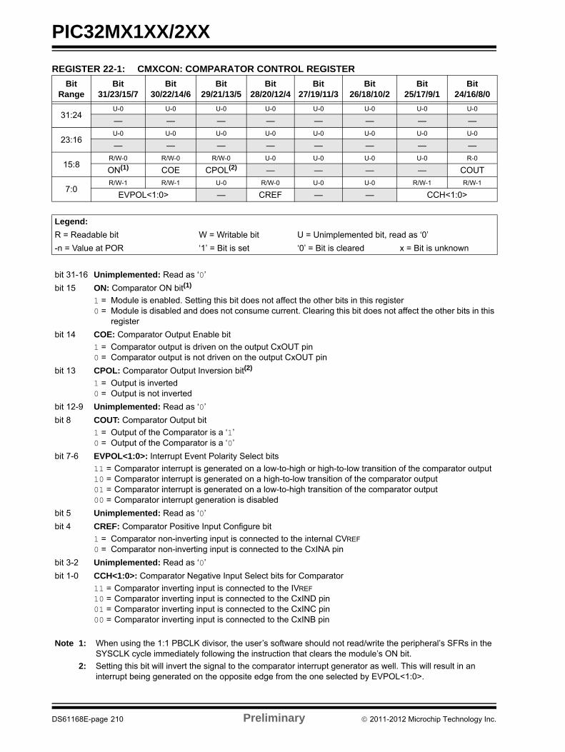
PIC32MX1XX/2XX
REGISTER 22-1: CMXCON: COMPARATOR CONTROL REGISTER
Bit Range
Bit31/23/15/7
Bit30/22/14/6
Bit29/21/13/5
Bit28/20/12/4
Bit27/19/11/3
Bit26/18/10/2
Bit25/17/9/1
Bit24/16/8/0
31:24U-0 U-0 U-0 U-0 U-0 U-0 U-0 U-0
— — — — — — — —
23:16U-0 U-0 U-0 U-0 U-0 U-0 U-0 U-0
— — — — — — — —
15:8R/W-0 R/W-0 R/W-0 U-0 U-0 U-0 U-0 R-0
ON(1) COE CPOL(2) — — — — COUT
7:0R/W-1 R/W-1 U-0 R/W-0 U-0 U-0 R/W-1 R/W-1
EVPOL<1:0> — CREF — — CCH<1:0>
Legend:
R = Readable bit W = Writable bit U = Unimplemented bit, read as ‘0’
-n = Value at POR ‘1’ = Bit is set ‘0’ = Bit is cleared x = Bit is unknown
bit 31-16 Unimplemented: Read as ‘0’
bit 15 ON: Comparator ON bit(1)
1 = Module is enabled. Setting this bit does not affect the other bits in this register0 = Module is disabled and does not consume current. Clearing this bit does not affect the other bits in this
register
bit 14 COE: Comparator Output Enable bit
1 = Comparator output is driven on the output CxOUT pin0 = Comparator output is not driven on the output CxOUT pin
bit 13 CPOL: Comparator Output Inversion bit(2)
1 = Output is inverted0 = Output is not inverted
bit 12-9 Unimplemented: Read as ‘0’
bit 8 COUT: Comparator Output bit
1 = Output of the Comparator is a ‘1’0 = Output of the Comparator is a ‘0’
bit 7-6 EVPOL<1:0>: Interrupt Event Polarity Select bits
11 = Comparator interrupt is generated on a low-to-high or high-to-low transition of the comparator output10 = Comparator interrupt is generated on a high-to-low transition of the comparator output01 = Comparator interrupt is generated on a low-to-high transition of the comparator output00 = Comparator interrupt generation is disabled
bit 5 Unimplemented: Read as ‘0’
bit 4 CREF: Comparator Positive Input Configure bit
1 = Comparator non-inverting input is connected to the internal CVREF
0 = Comparator non-inverting input is connected to the CXINA pin
bit 3-2 Unimplemented: Read as ‘0’
bit 1-0 CCH<1:0>: Comparator Negative Input Select bits for Comparator
11 = Comparator inverting input is connected to the IVREF
10 = Comparator inverting input is connected to the CxIND pin01 = Comparator inverting input is connected to the CxINC pin00 = Comparator inverting input is connected to the CxINB pin
Note 1: When using the 1:1 PBCLK divisor, the user’s software should not read/write the peripheral’s SFRs in the SYSCLK cycle immediately following the instruction that clears the module’s ON bit.
2: Setting this bit will invert the signal to the comparator interrupt generator as well. This will result in an interrupt being generated on the opposite edge from the one selected by EVPOL<1:0>.
DS61168E-page 210 Preliminary 2011-2012 Microchip Technology Inc.
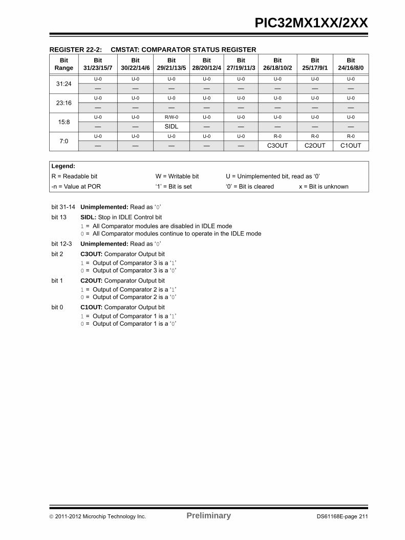
PIC32MX1XX/2XX
REGISTER 22-2: CMSTAT: COMPARATOR STATUS REGISTER
Bit Range
Bit31/23/15/7
Bit30/22/14/6
Bit29/21/13/5
Bit28/20/12/4
Bit27/19/11/3
Bit26/18/10/2
Bit25/17/9/1
Bit24/16/8/0
31:24U-0 U-0 U-0 U-0 U-0 U-0 U-0 U-0
— — — — — — — —
23:16U-0 U-0 U-0 U-0 U-0 U-0 U-0 U-0
— — — — — — — —
15:8U-0 U-0 R/W-0 U-0 U-0 U-0 U-0 U-0
— — SIDL — — — — —
7:0U-0 U-0 U-0 U-0 U-0 R-0 R-0 R-0
— — — — — C3OUT C2OUT C1OUT
Legend:
R = Readable bit W = Writable bit U = Unimplemented bit, read as ‘0’
-n = Value at POR ‘1’ = Bit is set ‘0’ = Bit is cleared x = Bit is unknown
bit 31-14 Unimplemented: Read as ‘0’
bit 13 SIDL: Stop in IDLE Control bit
1 = All Comparator modules are disabled in IDLE mode0 = All Comparator modules continue to operate in the IDLE mode
bit 12-3 Unimplemented: Read as ‘0’
bit 2 C3OUT: Comparator Output bit
1 = Output of Comparator 3 is a ‘1’0 = Output of Comparator 3 is a ‘0’
bit 1 C2OUT: Comparator Output bit
1 = Output of Comparator 2 is a ‘1’0 = Output of Comparator 2 is a ‘0’
bit 0 C1OUT: Comparator Output bit
1 = Output of Comparator 1 is a ‘1’0 = Output of Comparator 1 is a ‘0’
2011-2012 Microchip Technology Inc. Preliminary DS61168E-page 211

PIC32MX1XX/2XX
NOTES:
DS61168E-page 212 Preliminary 2011-2012 Microchip Technology Inc.
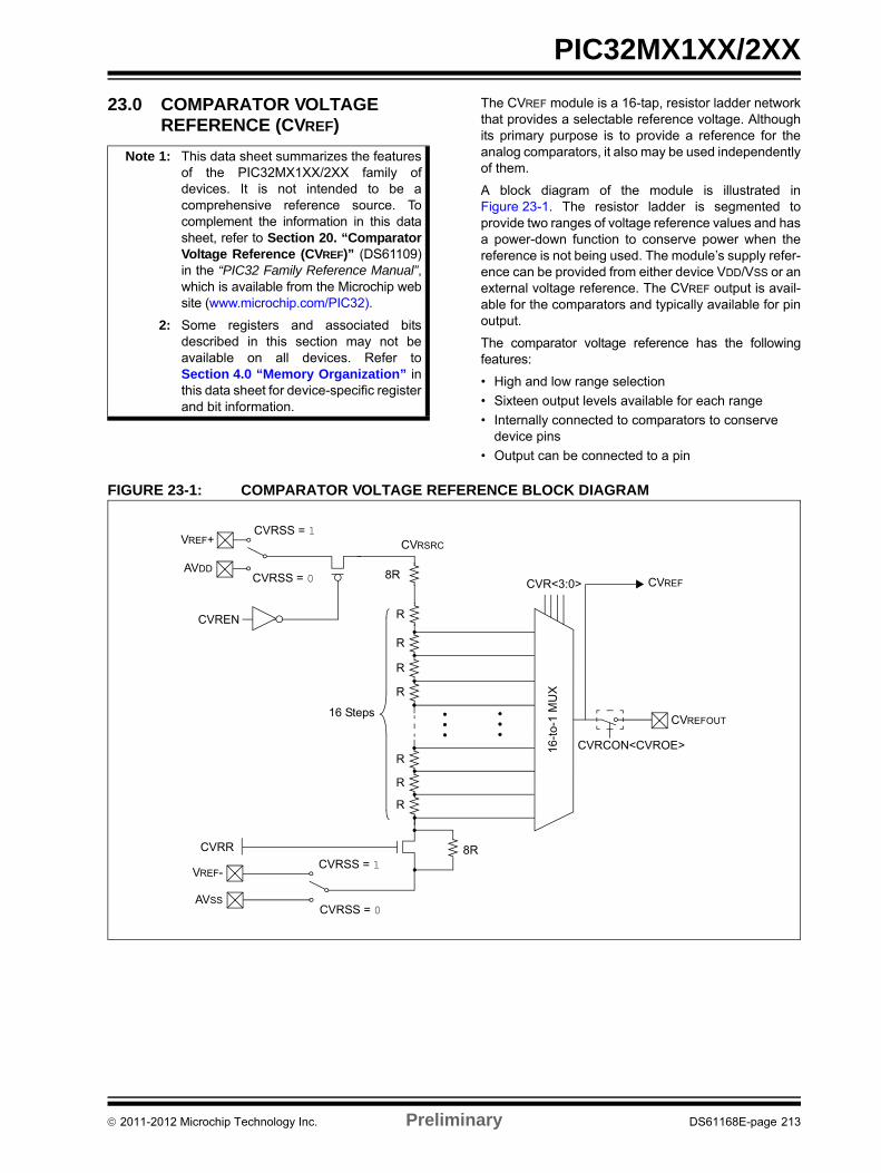
PIC32MX1XX/2XX
23.0 COMPARATOR VOLTAGE REFERENCE (CVREF)
The CVREF module is a 16-tap, resistor ladder networkthat provides a selectable reference voltage. Althoughits primary purpose is to provide a reference for theanalog comparators, it also may be used independentlyof them.
A block diagram of the module is illustrated inFigure 23-1. The resistor ladder is segmented toprovide two ranges of voltage reference values and hasa power-down function to conserve power when thereference is not being used. The module’s supply refer-ence can be provided from either device VDD/VSS or anexternal voltage reference. The CVREF output is avail-able for the comparators and typically available for pinoutput.
The comparator voltage reference has the followingfeatures:
• High and low range selection
• Sixteen output levels available for each range
• Internally connected to comparators to conserve device pins
• Output can be connected to a pin
FIGURE 23-1: COMPARATOR VOLTAGE REFERENCE BLOCK DIAGRAM
Note 1: This data sheet summarizes the featuresof the PIC32MX1XX/2XX family ofdevices. It is not intended to be acomprehensive reference source. Tocomplement the information in this datasheet, refer to Section 20. “ComparatorVoltage Reference (CVREF)” (DS61109)in the “PIC32 Family Reference Manual”,which is available from the Microchip website (www.microchip.com/PIC32).
2: Some registers and associated bitsdescribed in this section may not beavailable on all devices. Refer toSection 4.0 “Memory Organization” inthis data sheet for device-specific registerand bit information.
16-t
o-1
MU
X
CVR<3:0>8R
RCVREN
CVRSS = 0AVDD
VREF+CVRSS = 1
8R
CVRSS = 0
VREF-CVRSS = 1
R
R
R
R
R
R
16 Steps
CVRR
CVREFOUT
AVSS
CVRCON<CVROE>
CVREF
CVRSRC
2011-2012 Microchip Technology Inc. Preliminary DS61168E-page 213
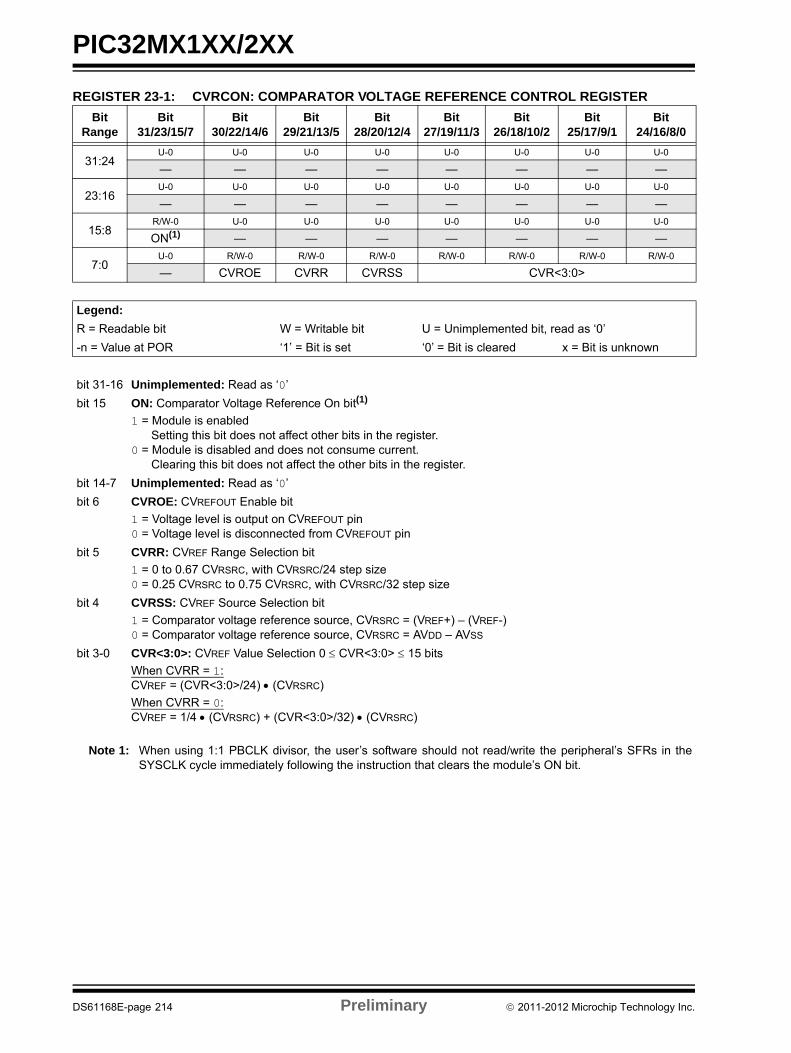
PIC32MX1XX/2XX
REGISTER 23-1: CVRCON: COMPARATOR VOLTAGE REFERENCE CONTROL REGISTER
Bit Range
Bit31/23/15/7
Bit30/22/14/6
Bit29/21/13/5
Bit28/20/12/4
Bit27/19/11/3
Bit26/18/10/2
Bit25/17/9/1
Bit24/16/8/0
31:24U-0 U-0 U-0 U-0 U-0 U-0 U-0 U-0
— — — — — — — —
23:16U-0 U-0 U-0 U-0 U-0 U-0 U-0 U-0
— — — — — — — —
15:8R/W-0 U-0 U-0 U-0 U-0 U-0 U-0 U-0
ON(1) — — — — — — —
7:0U-0 R/W-0 R/W-0 R/W-0 R/W-0 R/W-0 R/W-0 R/W-0
— CVROE CVRR CVRSS CVR<3:0>
Legend:
R = Readable bit W = Writable bit U = Unimplemented bit, read as ‘0’
-n = Value at POR ‘1’ = Bit is set ‘0’ = Bit is cleared x = Bit is unknown
bit 31-16 Unimplemented: Read as ‘0’
bit 15 ON: Comparator Voltage Reference On bit(1)
1 = Module is enabledSetting this bit does not affect other bits in the register.
0 = Module is disabled and does not consume current. Clearing this bit does not affect the other bits in the register.
bit 14-7 Unimplemented: Read as ‘0’
bit 6 CVROE: CVREFOUT Enable bit
1 = Voltage level is output on CVREFOUT pin0 = Voltage level is disconnected from CVREFOUT pin
bit 5 CVRR: CVREF Range Selection bit
1 = 0 to 0.67 CVRSRC, with CVRSRC/24 step size 0 = 0.25 CVRSRC to 0.75 CVRSRC, with CVRSRC/32 step size
bit 4 CVRSS: CVREF Source Selection bit
1 = Comparator voltage reference source, CVRSRC = (VREF+) – (VREF-) 0 = Comparator voltage reference source, CVRSRC = AVDD – AVSS
bit 3-0 CVR<3:0>: CVREF Value Selection 0 CVR<3:0> 15 bits
When CVRR = 1:CVREF = (CVR<3:0>/24) (CVRSRC)
When CVRR = 0:CVREF = 1/4 (CVRSRC) + (CVR<3:0>/32) (CVRSRC)
Note 1: When using 1:1 PBCLK divisor, the user’s software should not read/write the peripheral’s SFRs in theSYSCLK cycle immediately following the instruction that clears the module’s ON bit.
DS61168E-page 214 Preliminary 2011-2012 Microchip Technology Inc.
PIC32MX1XX/2XX
24.0 CHARGE TIME MEASUREMENT UNIT (CTMU)
The Charge Time Measurement Unit (CTMU) is a flex-ible analog module that has a configurable currentsource with a digital configuration circuit built around it.The CTMU can be used for differential time measure-ment between pulse sources and can be used for gen-erating an asynchronous pulse. By working with other
on-chip analog modules, the CTMU can be used forhigh resolution time measurement, measure capaci-tance, measure relative changes in capacitance orgenerate output pulses with a specific time delay. TheCTMU is ideal for interfacing with capacitive-basedsensors.
The module includes the following key features:
• Up to 13 channels available for capacitive or time measurement input
• On-chip precision current source
• 16-edge input trigger sources
• Selection of edge or level-sensitive inputs
• Polarity control for each edge source
• Control of edge sequence
• Control of response to edges
• High precision time measurement
• Time delay of external or internal signal asynchro-nous to system clock
• Integrated temperature sensing diode
• Control of current source during auto-sampling
• Four current source ranges
• Time measurement resolution of one nanosecond
A block diagram of the CTMU is shown in Figure 24-1.
FIGURE 24-1: CTMU BLOCK DIAGRAM
Note 1: This data sheet summarizes the fea-tures of the PIC32MX1XX/2XX family ofdevices. It is not intended to be acomprehensive reference source. Tocomplement the information in this datasheet, refer to Section 37. “ChargeTime Measurement Unit (CTMU)”(DS61167) in the “PIC32 FamilyReference Manual”, which is availablefrom the Microchip web site(www.microchip.com).
2: Some registers and associated bitsdescribed in this section may not beavailable on all devices. Refer toSection 4.0 “Memory Organization” inthis data sheet for device-specific registerand bit information.
CTED1
CTED13
Current Source
EdgeControlLogic
CTMUCON1 or CTMUCON2
PulseGenerator
CTMUI
Comparator 2
Timer1OC1
CurrentControl
ITRIM<5:0>IRNG<1:0>
CTMUICON
CTMUControlLogic
EDG1STATEDG2STAT
ADC
CTPLSIC1-IC3CMP1-CMP3
C2INB
CDelay
CTMUT
TemperatureSensor
Current Control Selection TGEN EDG1STAT, EDG2STAT
CTMUT 0 EDG1STAT = EDG2STAT
CTMUI 0 EDG1STAT EDG2STAT
CTMUP 1 EDG1STAT EDG2STAT
No Connect 1 EDG1STAT = EDG2STAT
TriggerTGEN
CTMUP
External capacitorfor pulse generation
(To ADC S&H capacitor)
(To ADC)
PBCLK
•••
2011-2012 Microchip Technology Inc. Preliminary DS61168E-page 215
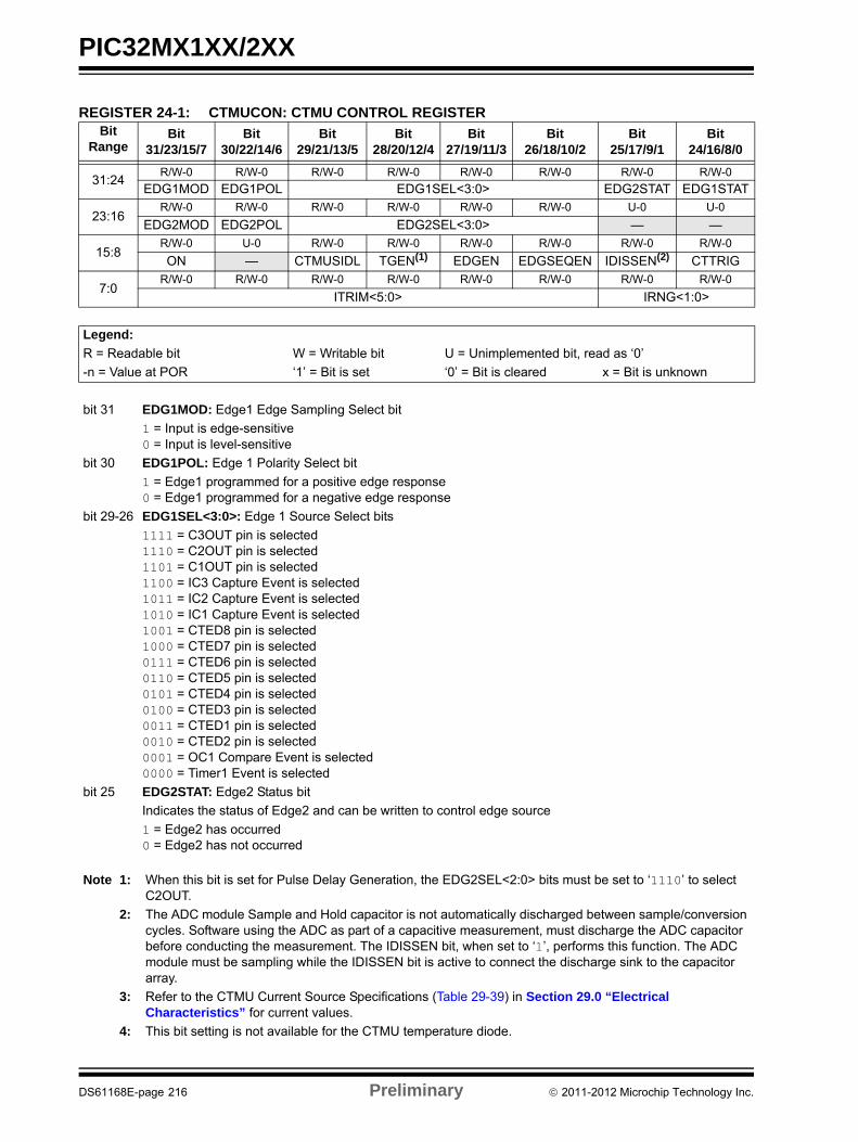
PIC32MX1XX/2XX
REGISTER 24-1: CTMUCON: CTMU CONTROL REGISTERBit
RangeBit
31/23/15/7Bit
30/22/14/6Bit
29/21/13/5Bit
28/20/12/4Bit
27/19/11/3Bit
26/18/10/2Bit
25/17/9/1Bit
24/16/8/0
31:24R/W-0 R/W-0 R/W-0 R/W-0 R/W-0 R/W-0 R/W-0 R/W-0
EDG1MOD EDG1POL EDG1SEL<3:0> EDG2STAT EDG1STAT
23:16R/W-0 R/W-0 R/W-0 R/W-0 R/W-0 R/W-0 U-0 U-0
EDG2MOD EDG2POL EDG2SEL<3:0> — —
15:8R/W-0 U-0 R/W-0 R/W-0 R/W-0 R/W-0 R/W-0 R/W-0
ON — CTMUSIDL TGEN(1) EDGEN EDGSEQEN IDISSEN(2) CTTRIG
7:0R/W-0 R/W-0 R/W-0 R/W-0 R/W-0 R/W-0 R/W-0 R/W-0
ITRIM<5:0> IRNG<1:0>
Legend:
R = Readable bit W = Writable bit U = Unimplemented bit, read as ‘0’
-n = Value at POR ‘1’ = Bit is set ‘0’ = Bit is cleared x = Bit is unknown
bit 31 EDG1MOD: Edge1 Edge Sampling Select bit
1 = Input is edge-sensitive0 = Input is level-sensitive
bit 30 EDG1POL: Edge 1 Polarity Select bit
1 = Edge1 programmed for a positive edge response0 = Edge1 programmed for a negative edge response
bit 29-26 EDG1SEL<3:0>: Edge 1 Source Select bits
1111 = C3OUT pin is selected1110 = C2OUT pin is selected1101 = C1OUT pin is selected1100 = IC3 Capture Event is selected1011 = IC2 Capture Event is selected1010 = IC1 Capture Event is selected1001 = CTED8 pin is selected1000 = CTED7 pin is selected0111 = CTED6 pin is selected0110 = CTED5 pin is selected0101 = CTED4 pin is selected0100 = CTED3 pin is selected0011 = CTED1 pin is selected0010 = CTED2 pin is selected0001 = OC1 Compare Event is selected0000 = Timer1 Event is selected
bit 25 EDG2STAT: Edge2 Status bit
Indicates the status of Edge2 and can be written to control edge source
1 = Edge2 has occurred0 = Edge2 has not occurred
Note 1: When this bit is set for Pulse Delay Generation, the EDG2SEL<2:0> bits must be set to ‘1110’ to select C2OUT.
2: The ADC module Sample and Hold capacitor is not automatically discharged between sample/conversion cycles. Software using the ADC as part of a capacitive measurement, must discharge the ADC capacitor before conducting the measurement. The IDISSEN bit, when set to ‘1’, performs this function. The ADC module must be sampling while the IDISSEN bit is active to connect the discharge sink to the capacitor array.
3: Refer to the CTMU Current Source Specifications (Table 29-39) in Section 29.0 “Electrical Characteristics” for current values.
4: This bit setting is not available for the CTMU temperature diode.
DS61168E-page 216 Preliminary 2011-2012 Microchip Technology Inc.
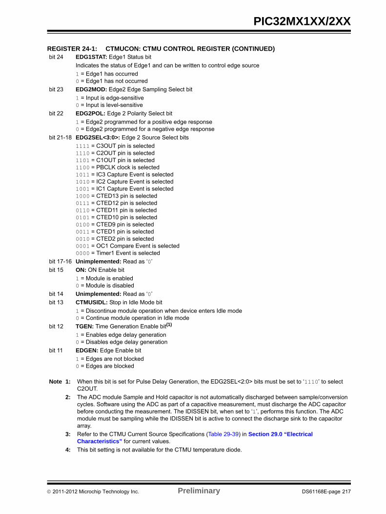
PIC32MX1XX/2XX
bit 24 EDG1STAT: Edge1 Status bit
Indicates the status of Edge1 and can be written to control edge source
1 = Edge1 has occurred0 = Edge1 has not occurred
bit 23 EDG2MOD: Edge2 Edge Sampling Select bit
1 = Input is edge-sensitive0 = Input is level-sensitive
bit 22 EDG2POL: Edge 2 Polarity Select bit
1 = Edge2 programmed for a positive edge response0 = Edge2 programmed for a negative edge response
bit 21-18 EDG2SEL<3:0>: Edge 2 Source Select bits
1111 = C3OUT pin is selected1110 = C2OUT pin is selected1101 = C1OUT pin is selected1100 = PBCLK clock is selected1011 = IC3 Capture Event is selected1010 = IC2 Capture Event is selected1001 = IC1 Capture Event is selected1000 = CTED13 pin is selected0111 = CTED12 pin is selected0110 = CTED11 pin is selected0101 = CTED10 pin is selected0100 = CTED9 pin is selected0011 = CTED1 pin is selected0010 = CTED2 pin is selected0001 = OC1 Compare Event is selected0000 = Timer1 Event is selected
bit 17-16 Unimplemented: Read as ‘0’
bit 15 ON: ON Enable bit
1 = Module is enabled0 = Module is disabled
bit 14 Unimplemented: Read as ‘0’
bit 13 CTMUSIDL: Stop in Idle Mode bit
1 = Discontinue module operation when device enters Idle mode0 = Continue module operation in Idle mode
bit 12 TGEN: Time Generation Enable bit(1)
1 = Enables edge delay generation0 = Disables edge delay generation
bit 11 EDGEN: Edge Enable bit
1 = Edges are not blocked0 = Edges are blocked
REGISTER 24-1: CTMUCON: CTMU CONTROL REGISTER (CONTINUED)
Note 1: When this bit is set for Pulse Delay Generation, the EDG2SEL<2:0> bits must be set to ‘1110’ to select C2OUT.
2: The ADC module Sample and Hold capacitor is not automatically discharged between sample/conversion cycles. Software using the ADC as part of a capacitive measurement, must discharge the ADC capacitor before conducting the measurement. The IDISSEN bit, when set to ‘1’, performs this function. The ADC module must be sampling while the IDISSEN bit is active to connect the discharge sink to the capacitor array.
3: Refer to the CTMU Current Source Specifications (Table 29-39) in Section 29.0 “Electrical Characteristics” for current values.
4: This bit setting is not available for the CTMU temperature diode.
2011-2012 Microchip Technology Inc. Preliminary DS61168E-page 217
PIC32MX1XX/2XX
bit 10 EDGSEQEN: Edge Sequence Enable bit
1 = Edge1 must occur before Edge2 can occur0 = No edge sequence is needed
bit 9 IDISSEN: Analog Current Source Control bit(2)
1 = Analog current source output is grounded0 = Analog current source output is not grounded
bit 8 CTTRIG: Trigger Control bit 1 = Trigger output is enabled0 = Trigger output is disabled
bit 7-2 ITRIM<5:0>: Current Source Trim bits
011111 = Maximum positive change from nominal current011110 •••
000001 = Minimum positive change from nominal current000000 = Nominal current output specified by IRNG<1:0>111111 = Minimum negative change from nominal current•••
100010 100001 = Maximum negative change from nominal current
bit 1-0 IRNG<1:0>: Current Range Select bits(3)
11 = 100 times base current10 = 10 times base current01 = Base current level00 = 1000 times base current(4)
REGISTER 24-1: CTMUCON: CTMU CONTROL REGISTER (CONTINUED)
Note 1: When this bit is set for Pulse Delay Generation, the EDG2SEL<2:0> bits must be set to ‘1110’ to select C2OUT.
2: The ADC module Sample and Hold capacitor is not automatically discharged between sample/conversion cycles. Software using the ADC as part of a capacitive measurement, must discharge the ADC capacitor before conducting the measurement. The IDISSEN bit, when set to ‘1’, performs this function. The ADC module must be sampling while the IDISSEN bit is active to connect the discharge sink to the capacitor array.
3: Refer to the CTMU Current Source Specifications (Table 29-39) in Section 29.0 “Electrical Characteristics” for current values.
4: This bit setting is not available for the CTMU temperature diode.
DS61168E-page 218 Preliminary 2011-2012 Microchip Technology Inc.
PIC32MX1XX/2XX
25.0 POWER-SAVING FEATURES
This section describes power-saving features for thePIC32MX1XX/2XX. The PIC32 devices offer a total ofnine methods and modes, organized into twocategories, that allow the user to balance powerconsumption with device performance. In all of themethods and modes described in this section, power-saving is controlled by software.
25.1 Power Saving with CPU Running
When the CPU is running, power consumption can becontrolled by reducing the CPU clock frequency,lowering the PBCLK and by individually disablingmodules. These methods are grouped into thefollowing categories:
• FRC Run mode: the CPU is clocked from the FRC clock source with or without postscalers.
• LPRC Run mode: the CPU is clocked from the LPRC clock source.
• SOSC Run mode: the CPU is clocked from the SOSC clock source.
In addition, the Peripheral Bus Scaling mode is availablewhere peripherals are clocked at the programmablefraction of the CPU clock (SYSCLK).
25.2 CPU Halted Methods
The device supports two power-saving modes, Sleepand Idle, both of which Halt the clock to the CPU. Thesemodes operate with all clock sources, as listed below:
• POSC Idle mode: the system clock is derived from the POSC. The system clock source continues to operate. Peripherals continue to operate, but can optionally be individually disabled.
• FRC Idle mode: the system clock is derived from the FRC with or without postscalers. Peripherals continue to operate, but can optionally be individually disabled.
• SOSC Idle mode: the system clock is derived from the SOSC. Peripherals continue to operate, but can optionally be individually disabled.
• LPRC Idle mode: the system clock is derived from the LPRC. Peripherals continue to operate, but can optionally be individually disabled. This is the lowest power mode for the device with a clock running.
• Sleep mode: the CPU, the system clock source and any peripherals that operate from the system clock source are Halted. Some peripherals can operate in Sleep using specific clock sources. This is the lowest power mode for the device.
25.3 Power-Saving Operation
Peripherals and the CPU can be Halted or disabled tofurther reduce power consumption.
25.3.1 SLEEP MODE
Sleep mode has the lowest power consumption of thedevice power-saving operating modes. The CPU andmost peripherals are Halted. Select peripherals cancontinue to operate in Sleep mode and can be used towake the device from Sleep. See the individualperipheral module sections for descriptions ofbehavior in Sleep.
Sleep mode includes the following characteristics:
• The CPU is Halted.
• The system clock source is typically shutdown. See Section 25.3.3 “Peripheral Bus Scaling Method” for specific information.
• There can be a wake-up delay based on the oscillator selection.
• The Fail-Safe Clock Monitor (FSCM) does not operate during Sleep mode.
• The BOR circuit remains operative during Sleep mode.
• The WDT, if enabled, is not automatically cleared prior to entering Sleep mode.
• Some peripherals can continue to operate at limited functionality in Sleep mode. These peripherals include I/O pins that detect a change in the input signal, WDT, ADC, UART and peripherals that use an external clock input or the internal LPRC oscillator (e.g., RTCC, Timer1 and Input Capture).
• I/O pins continue to sink or source current in the same manner as they do when the device is not in Sleep.
• The USB module can override the disabling of the Posc or FRC. Refer to the USB section for specific details.
• Modules can be individually disabled by software prior to entering Sleep in order to further reduce consumption.
Note 1: This data sheet summarizes the featuresof the PIC32MX1XX/2XX family ofdevices. It is not intended to be acomprehensive reference source. Tocomplement the information in this datasheet, refer to Section 10. “Power-Saving Features” (DS61130) in the“PIC32 Family Reference Manual”, whichis available from the Microchip web site(www.microchip.com/PIC32).
2: Some registers and associated bitsdescribed in this section may not beavailable on all devices. Refer toSection 4.0 “Memory Organization” inthis data sheet for device-specific registerand bit information.
2011-2012 Microchip Technology Inc. Preliminary DS61168E-page 219
PIC32MX1XX/2XX
The processor will exit, or ‘wake-up’, from Sleep on oneof the following events:
• On any interrupt from an enabled source that is operating in Sleep. The interrupt priority must be greater than the current CPU priority.
• On any form of device Reset
• On a WDT time-out
If the interrupt priority is lower than or equal to thecurrent priority, the CPU will remain Halted, but thePBCLK will start running and the device will enter intoIdle mode.
25.3.2 IDLE MODE
In Idle mode, the CPU is Halted but the System Clock(SYSCLK) source is still enabled. This allows peripher-als to continue operation when the CPU is Halted.Peripherals can be individually configured to Halt whenentering Idle by setting their respective SIDL bit.Latency, when exiting Idle mode, is very low due to theCPU oscillator source remaining active.
The device enters Idle mode when the SLPEN bit(OSCCON<4>) is clear and a WAIT instruction isexecuted.
The processor will wake or exit from Idle mode on thefollowing events:
• On any interrupt event for which the interrupt source is enabled. The priority of the interrupt event must be greater than the current priority of the CPU. If the priority of the interrupt event is lower than or equal to current priority of the CPU, the CPU will remain Halted and the device will remain in Idle mode.
• On any form of device Reset
• On a WDT time-out interrupt
25.3.3 PERIPHERAL BUS SCALING METHOD
Most of the peripherals on the device are clocked usingthe PBCLK. The peripheral bus can be scaled relative tothe SYSCLK to minimize the dynamic power consumedby the peripherals. The PBCLK divisor is controlled byPBDIV<1:0> (OSCCON<20:19>), allowing SYSCLK toPBCLK ratios of 1:1, 1:2, 1:4 and 1:8. All peripheralsusing PBCLK are affected when the divisor is changed.Peripherals such as the USB, Interrupt Controller, DMA,and the bus matrix are clocked directly from SYSCLK.As a result, they are not affected by PBCLK divisorchanges.
Changing the PBCLK divisor affects:
• The CPU to peripheral access latency. The CPU has to wait for next PBCLK edge for a read to complete. In 1:8 mode, this results in a latency of one to seven SYSCLKs.
• The power consumption of the peripherals. Power consumption is directly proportional to the fre-quency at which the peripherals are clocked. The greater the divisor, the lower the power consumed by the peripherals.
To minimize dynamic power, the PB divisor should bechosen to run the peripherals at the lowest frequencythat provides acceptable system performance. Whenselecting a PBCLK divider, peripheral clock require-ments, such as baud rate accuracy, should be takeninto account. For example, the UART peripheral maynot be able to achieve all baud rate values at somePBCLK divider depending on the SYSCLK value.
Note 1: Changing the PBCLK divider ratiorequires recalculation of peripheral tim-ing. For example, assume the UART isconfigured for 9600 baud with a PB clockratio of 1:1 and a POSC of 8 MHz. Whenthe PB clock divisor of 1:2 is used, theinput frequency to the baud clock is cut inhalf; therefore, the baud rate is reducedto 1/2 its former value. Due to numerictruncation in calculations (such as thebaud rate divisor), the actual baud ratemay be a tiny percentage different thanexpected. For this reason, any timing cal-culation required for a peripheral shouldbe performed with the new PB clock fre-quency instead of scaling the previousvalue based on a change in the PB divisorratio.
2: Oscillator start-up and PLL lock delaysare applied when switching to a clocksource that was disabled and that uses acrystal and/or the PLL. For example,assume the clock source is switched fromPOSC to LPRC just prior to entering Sleepin order to save power. No oscillator start-up delay would be applied when exitingIdle. However, when switching back toPOSC, the appropriate PLL and/oroscillator start-up/lock delays would beapplied.
DS61168E-page 220 Preliminary 2011-2012 Microchip Technology Inc.
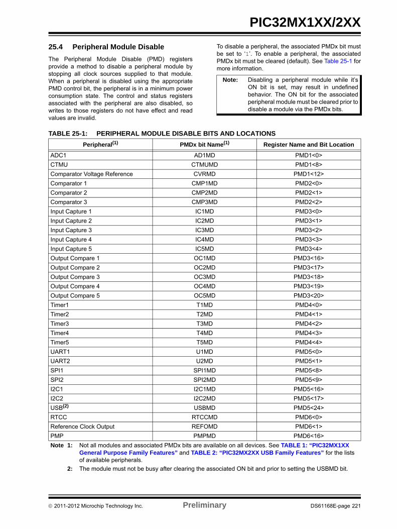
PIC32MX1XX/2XX
25.4 Peripheral Module Disable
The Peripheral Module Disable (PMD) registersprovide a method to disable a peripheral module bystopping all clock sources supplied to that module.When a peripheral is disabled using the appropriatePMD control bit, the peripheral is in a minimum powerconsumption state. The control and status registersassociated with the peripheral are also disabled, sowrites to those registers do not have effect and readvalues are invalid.
To disable a peripheral, the associated PMDx bit mustbe set to ‘1’. To enable a peripheral, the associatedPMDx bit must be cleared (default). See Table 25-1 formore information.
TABLE 25-1: PERIPHERAL MODULE DISABLE BITS AND LOCATIONS
Note: Disabling a peripheral module while it’sON bit is set, may result in undefinedbehavior. The ON bit for the associatedperipheral module must be cleared prior todisable a module via the PMDx bits.
Peripheral(1) PMDx bit Name(1) Register Name and Bit Location
ADC1 AD1MD PMD1<0>
CTMU CTMUMD PMD1<8>
Comparator Voltage Reference CVRMD PMD1<12>
Comparator 1 CMP1MD PMD2<0>
Comparator 2 CMP2MD PMD2<1>
Comparator 3 CMP3MD PMD2<2>
Input Capture 1 IC1MD PMD3<0>
Input Capture 2 IC2MD PMD3<1>
Input Capture 3 IC3MD PMD3<2>
Input Capture 4 IC4MD PMD3<3>
Input Capture 5 IC5MD PMD3<4>
Output Compare 1 OC1MD PMD3<16>
Output Compare 2 OC2MD PMD3<17>
Output Compare 3 OC3MD PMD3<18>
Output Compare 4 OC4MD PMD3<19>
Output Compare 5 OC5MD PMD3<20>
Timer1 T1MD PMD4<0>
Timer2 T2MD PMD4<1>
Timer3 T3MD PMD4<2>
Timer4 T4MD PMD4<3>
Timer5 T5MD PMD4<4>
UART1 U1MD PMD5<0>
UART2 U2MD PMD5<1>
SPI1 SPI1MD PMD5<8>
SPI2 SPI2MD PMD5<9>
I2C1 I2C1MD PMD5<16>
I2C2 I2C2MD PMD5<17>
USB(2) USBMD PMD5<24>
RTCC RTCCMD PMD6<0>
Reference Clock Output REFOMD PMD6<1>
PMP PMPMD PMD6<16>
Note 1: Not all modules and associated PMDx bits are available on all devices. See TABLE 1: “PIC32MX1XX General Purpose Family Features” and TABLE 2: “PIC32MX2XX USB Family Features” for the lists of available peripherals.
2: The module must not be busy after clearing the associated ON bit and prior to setting the USBMD bit.
2011-2012 Microchip Technology Inc. Preliminary DS61168E-page 221
PIC32MX1XX/2XX
25.4.1 CONTROLLING CONFIGURATION CHANGES
Because peripherals can be disabled during run time,some restrictions on disabling peripherals are neededto prevent accidental configuration changes. PIC32devices include two features to prevent alterations toenabled or disabled peripherals:
• Control register lock sequence
• Configuration bit select lock
25.4.1.1 Control Register Lock
Under normal operation, writes to the PMDx registersare not allowed. Attempted writes appear to executenormally, but the contents of the registers remainunchanged. To change these registers, they must beunlocked in hardware. The register lock is controlled bythe PMDLOCK Configuration bit (CFGCON<12>). Set-ting PMDLOCK prevents writes to the control registers; clearing PMDLOCK allows writes.
To set or clear PMDLOCK, an unlock sequence mustbe executed. Refer to Section 6. “Oscillator”(DS61112) in the “PIC32 Family Reference Manual” fordetails.
25.4.1.2 Configuration Bit Select Lock
As an additional level of safety, the device can beconfigured to prevent more than one write session tothe PMDx registers. The PMDL1WAY Configuration bit(DEVCFG3<28>) blocks the PMDLOCK bit from beingcleared after it has been set once. If PMDLOCKremains set, the register unlock procedure does notexecute, and the peripheral pin select control registerscannot be written to. The only way to clear the bit andre-enable PMD functionality is to perform a deviceReset.
DS61168E-page 222 Preliminary 2011-2012 Microchip Technology Inc.
PIC32MX1XX/2XX
26.0 SPECIAL FEATURES
PIC32MX1XX/2XX devices include several featuresintended to maximize application flexibility and reliabil-ity and minimize cost through elimination of externalcomponents. These are:
• Flexible device configuration
• Watchdog Timer (WDT)
• Joint Test Action Group (JTAG) interface
• In-Circuit Serial Programming™ (ICSP™)
26.1 Configuration Bits
The Configuration bits can be programmed using thefollowing registers to select various deviceconfigurations.
• DEVCFG0: Device Configuration Word 0
• DEVCFG1: Device Configuration Word 1
• DEVCFG2: Device Configuration Word 2
• DEVCFG3: Device Configuration Word 3
• CFGCON: Configuration Control Register
In addition, the DEVID register (Register 26-6)provides device and revision information.
Note: This data sheet summarizes the featuresof the PIC32MX1XX/2XX family ofdevices. However, it is not intended to bea comprehensive reference source. Tocomplement the information in this datasheet, refer to Section 9. “WatchdogTimer and Power-up Timer” (DS61114),Section 32. “Configuration” (DS61124)and Section 33. “Programming andDiagnostics” (DS61129) in the “PIC32Family Reference Manual” (DS61132),which is available from the Microchip website (www.microchip.com/PIC32).
2011-2012 Microchip Technology Inc. Preliminary DS61168E-page 223
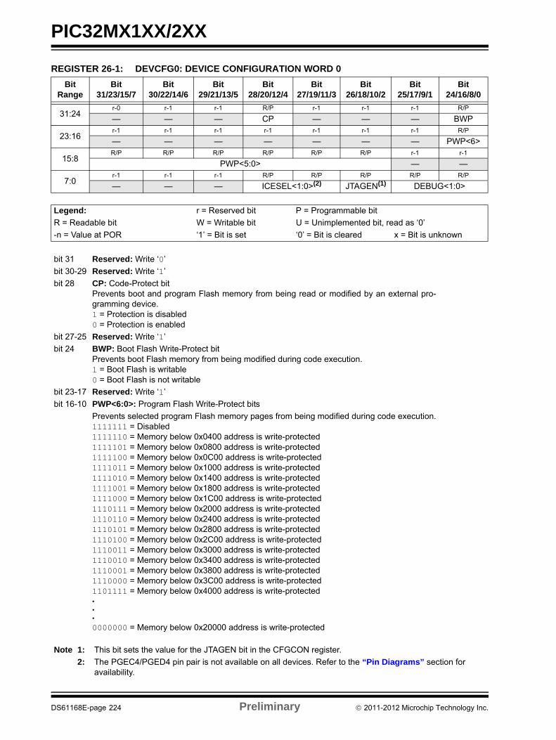
PIC32MX1XX/2XX
REGISTER 26-1: DEVCFG0: DEVICE CONFIGURATION WORD 0
Bit Range
Bit31/23/15/7
Bit30/22/14/6
Bit29/21/13/5
Bit28/20/12/4
Bit27/19/11/3
Bit26/18/10/2
Bit25/17/9/1
Bit24/16/8/0
31:24r-0 r-1 r-1 R/P r-1 r-1 r-1 R/P
— — — CP — — — BWP
23:16r-1 r-1 r-1 r-1 r-1 r-1 r-1 R/P
— — — — — — — PWP<6>
15:8R/P R/P R/P R/P R/P R/P r-1 r-1
PWP<5:0> — —
7:0r-1 r-1 r-1 R/P R/P R/P R/P R/P
— — — ICESEL<1:0>(2) JTAGEN(1) DEBUG<1:0>
Legend: r = Reserved bit P = Programmable bit
R = Readable bit W = Writable bit U = Unimplemented bit, read as ‘0’
-n = Value at POR ‘1’ = Bit is set ‘0’ = Bit is cleared x = Bit is unknown
bit 31 Reserved: Write ‘0’
bit 30-29 Reserved: Write ‘1’
bit 28 CP: Code-Protect bitPrevents boot and program Flash memory from being read or modified by an external pro-gramming device.1 = Protection is disabled0 = Protection is enabled
bit 27-25 Reserved: Write ‘1’
bit 24 BWP: Boot Flash Write-Protect bitPrevents boot Flash memory from being modified during code execution.1 = Boot Flash is writable0 = Boot Flash is not writable
bit 23-17 Reserved: Write ‘1’
bit 16-10 PWP<6:0>: Program Flash Write-Protect bits
Prevents selected program Flash memory pages from being modified during code execution.1111111 = Disabled1111110 = Memory below 0x0400 address is write-protected1111101 = Memory below 0x0800 address is write-protected1111100 = Memory below 0x0C00 address is write-protected1111011 = Memory below 0x1000 address is write-protected1111010 = Memory below 0x1400 address is write-protected1111001 = Memory below 0x1800 address is write-protected1111000 = Memory below 0x1C00 address is write-protected1110111 = Memory below 0x2000 address is write-protected1110110 = Memory below 0x2400 address is write-protected1110101 = Memory below 0x2800 address is write-protected1110100 = Memory below 0x2C00 address is write-protected1110011 = Memory below 0x3000 address is write-protected1110010 = Memory below 0x3400 address is write-protected1110001 = Memory below 0x3800 address is write-protected1110000 = Memory below 0x3C00 address is write-protected1101111 = Memory below 0x4000 address is write-protected•••
0000000 = Memory below 0x20000 address is write-protected
Note 1: This bit sets the value for the JTAGEN bit in the CFGCON register.
2: The PGEC4/PGED4 pin pair is not available on all devices. Refer to the “Pin Diagrams” section for availability.
DS61168E-page 224 Preliminary 2011-2012 Microchip Technology Inc.
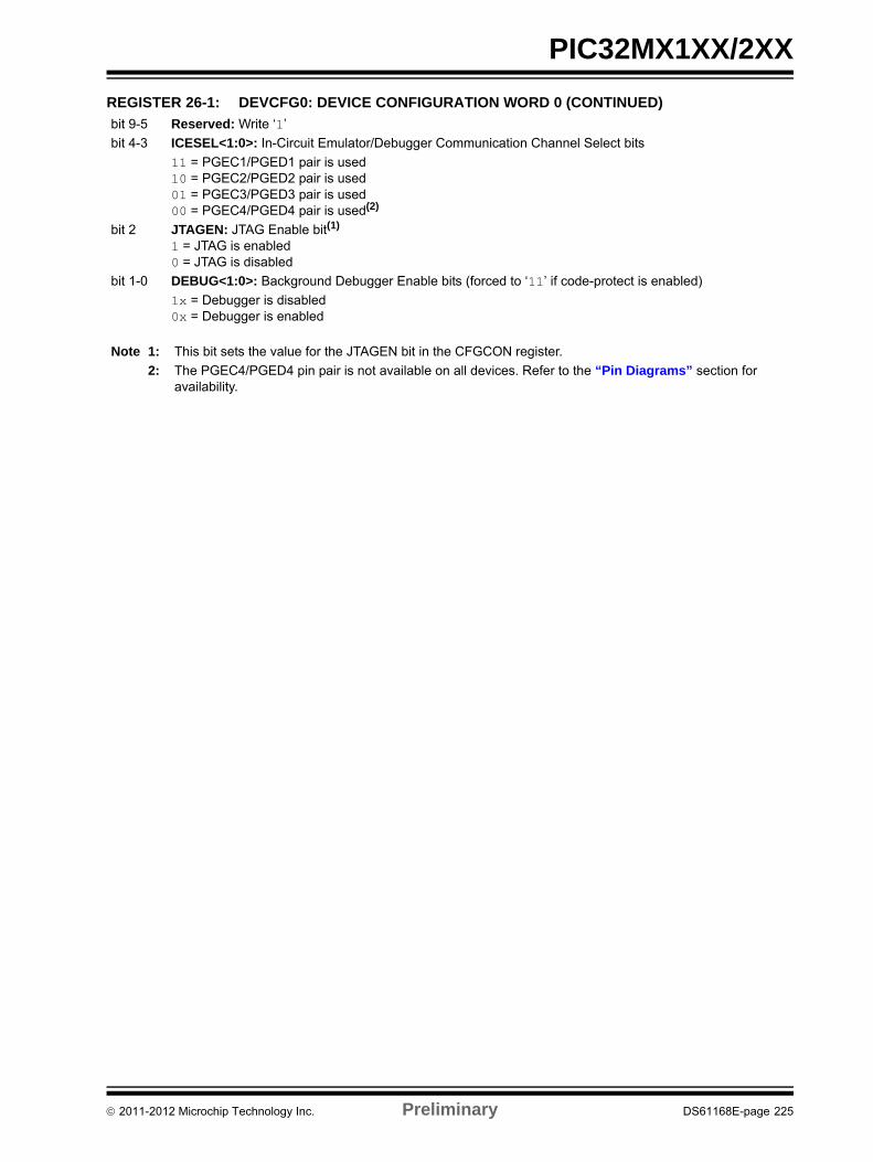
PIC32MX1XX/2XX
bit 9-5 Reserved: Write ‘1’
bit 4-3 ICESEL<1:0>: In-Circuit Emulator/Debugger Communication Channel Select bits
11 = PGEC1/PGED1 pair is used10 = PGEC2/PGED2 pair is used01 = PGEC3/PGED3 pair is used00 = PGEC4/PGED4 pair is used(2)
bit 2 JTAGEN: JTAG Enable bit(1)
1 = JTAG is enabled0 = JTAG is disabled
bit 1-0 DEBUG<1:0>: Background Debugger Enable bits (forced to ‘11’ if code-protect is enabled)
1x = Debugger is disabled0x = Debugger is enabled
REGISTER 26-1: DEVCFG0: DEVICE CONFIGURATION WORD 0 (CONTINUED)
Note 1: This bit sets the value for the JTAGEN bit in the CFGCON register.
2: The PGEC4/PGED4 pin pair is not available on all devices. Refer to the “Pin Diagrams” section for availability.
2011-2012 Microchip Technology Inc. Preliminary DS61168E-page 225
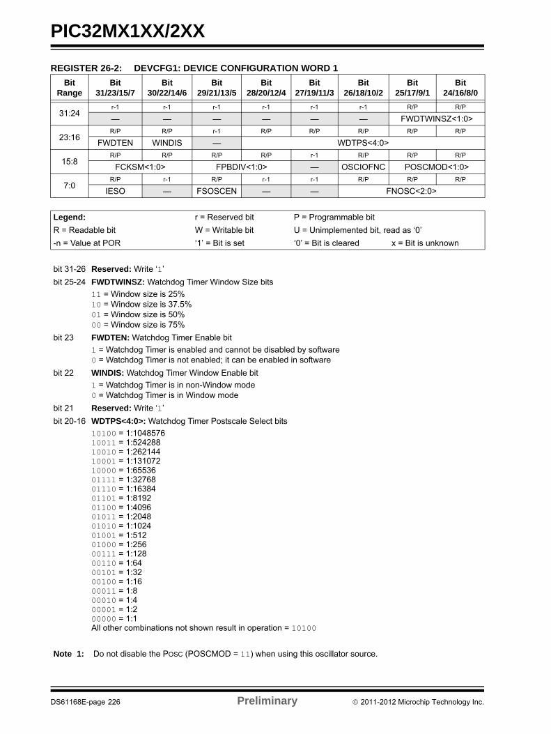
PIC32MX1XX/2XX
REGISTER 26-2: DEVCFG1: DEVICE CONFIGURATION WORD 1
Bit Range
Bit31/23/15/7
Bit30/22/14/6
Bit29/21/13/5
Bit28/20/12/4
Bit27/19/11/3
Bit26/18/10/2
Bit25/17/9/1
Bit24/16/8/0
31:24r-1 r-1 r-1 r-1 r-1 r-1 R/P R/P
— — — — — — FWDTWINSZ<1:0>
23:16R/P R/P r-1 R/P R/P R/P R/P R/P
FWDTEN WINDIS — WDTPS<4:0>
15:8R/P R/P R/P R/P r-1 R/P R/P R/P
FCKSM<1:0> FPBDIV<1:0> — OSCIOFNC POSCMOD<1:0>
7:0R/P r-1 R/P r-1 r-1 R/P R/P R/P
IESO — FSOSCEN — — FNOSC<2:0>
Legend: r = Reserved bit P = Programmable bit
R = Readable bit W = Writable bit U = Unimplemented bit, read as ‘0’
-n = Value at POR ‘1’ = Bit is set ‘0’ = Bit is cleared x = Bit is unknown
bit 31-26 Reserved: Write ‘1’
bit 25-24 FWDTWINSZ: Watchdog Timer Window Size bits
11 = Window size is 25%10 = Window size is 37.5%01 = Window size is 50%00 = Window size is 75%
bit 23 FWDTEN: Watchdog Timer Enable bit
1 = Watchdog Timer is enabled and cannot be disabled by software0 = Watchdog Timer is not enabled; it can be enabled in software
bit 22 WINDIS: Watchdog Timer Window Enable bit
1 = Watchdog Timer is in non-Window mode0 = Watchdog Timer is in Window mode
bit 21 Reserved: Write ‘1’
bit 20-16 WDTPS<4:0>: Watchdog Timer Postscale Select bits
10100 = 1:104857610011 = 1:52428810010 = 1:26214410001 = 1:13107210000 = 1:6553601111 = 1:3276801110 = 1:1638401101 = 1:819201100 = 1:409601011 = 1:204801010 = 1:102401001 = 1:51201000 = 1:25600111 = 1:12800110 = 1:6400101 = 1:3200100 = 1:1600011 = 1:800010 = 1:400001 = 1:200000 = 1:1All other combinations not shown result in operation = 10100
Note 1: Do not disable the POSC (POSCMOD = 11) when using this oscillator source.
DS61168E-page 226 Preliminary 2011-2012 Microchip Technology Inc.
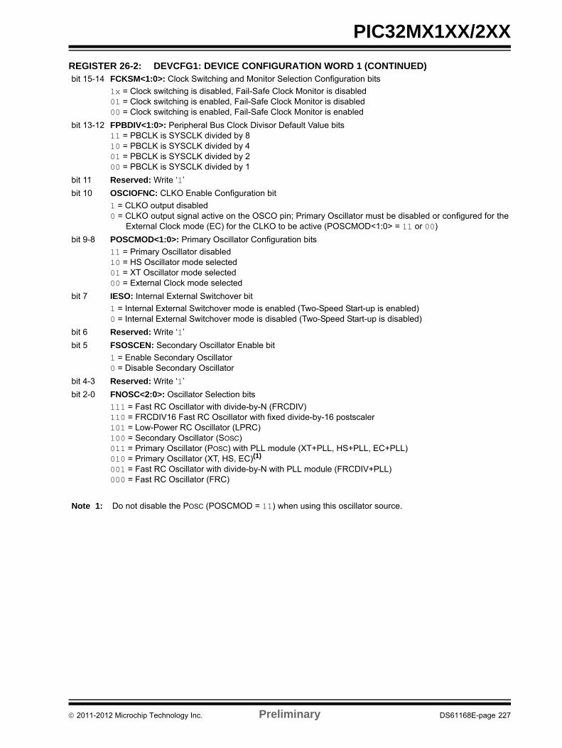
PIC32MX1XX/2XX
bit 15-14 FCKSM<1:0>: Clock Switching and Monitor Selection Configuration bits
1x = Clock switching is disabled, Fail-Safe Clock Monitor is disabled01 = Clock switching is enabled, Fail-Safe Clock Monitor is disabled00 = Clock switching is enabled, Fail-Safe Clock Monitor is enabled
bit 13-12 FPBDIV<1:0>: Peripheral Bus Clock Divisor Default Value bits11 = PBCLK is SYSCLK divided by 810 = PBCLK is SYSCLK divided by 401 = PBCLK is SYSCLK divided by 200 = PBCLK is SYSCLK divided by 1
bit 11 Reserved: Write ‘1’
bit 10 OSCIOFNC: CLKO Enable Configuration bit
1 = CLKO output disabled0 = CLKO output signal active on the OSCO pin; Primary Oscillator must be disabled or configured for the
External Clock mode (EC) for the CLKO to be active (POSCMOD<1:0> = 11 or 00)
bit 9-8 POSCMOD<1:0>: Primary Oscillator Configuration bits
11 = Primary Oscillator disabled10 = HS Oscillator mode selected01 = XT Oscillator mode selected00 = External Clock mode selected
bit 7 IESO: Internal External Switchover bit
1 = Internal External Switchover mode is enabled (Two-Speed Start-up is enabled)0 = Internal External Switchover mode is disabled (Two-Speed Start-up is disabled)
bit 6 Reserved: Write ‘1’
bit 5 FSOSCEN: Secondary Oscillator Enable bit
1 = Enable Secondary Oscillator0 = Disable Secondary Oscillator
bit 4-3 Reserved: Write ‘1’
bit 2-0 FNOSC<2:0>: Oscillator Selection bits
111 = Fast RC Oscillator with divide-by-N (FRCDIV)110 = FRCDIV16 Fast RC Oscillator with fixed divide-by-16 postscaler101 = Low-Power RC Oscillator (LPRC)100 = Secondary Oscillator (SOSC)011 = Primary Oscillator (POSC) with PLL module (XT+PLL, HS+PLL, EC+PLL) 010 = Primary Oscillator (XT, HS, EC)(1)
001 = Fast RC Oscillator with divide-by-N with PLL module (FRCDIV+PLL)000 = Fast RC Oscillator (FRC)
REGISTER 26-2: DEVCFG1: DEVICE CONFIGURATION WORD 1 (CONTINUED)
Note 1: Do not disable the POSC (POSCMOD = 11) when using this oscillator source.
2011-2012 Microchip Technology Inc. Preliminary DS61168E-page 227
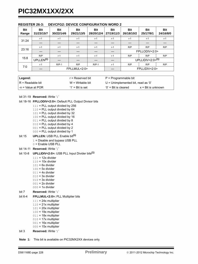
PIC32MX1XX/2XX
REGISTER 26-3: DEVCFG2: DEVICE CONFIGURATION WORD 2
Bit Range
Bit31/23/15/7
Bit30/22/14/6
Bit29/21/13/5
Bit28/20/12/4
Bit27/19/11/3
Bit26/18/10/2
Bit25/17/9/1
Bit24/16/8/0
31:24r-1 r-1 r-1 r-1 r-1 r-1 r-1 r-1
— — — — — — — —
23:16r-1 r-1 r-1 r-1 r-1 R/P R/P R/P
— — — — — FPLLODIV<2:0>
15:8R/P r-1 r-1 r-1 r-1 R/P R/P R/P
UPLLEN(1) — — — — UPLLIDIV<2:0>(1)
7:0r-1 R/P-1 R/P R/P-1 r-1 R/P R/P R/P
— FPLLMUL<2:0> — FPLLIDIV<2:0>
Legend: r = Reserved bit P = Programmable bit
R = Readable bit W = Writable bit U = Unimplemented bit, read as ‘0’
-n = Value at POR ‘1’ = Bit is set ‘0’ = Bit is cleared x = Bit is unknown
bit 31-19 Reserved: Write ‘1’
bit 18-16 FPLLODIV<2:0>: Default PLL Output Divisor bits
111 = PLL output divided by 256110 = PLL output divided by 64101 = PLL output divided by 32100 = PLL output divided by 16011 = PLL output divided by 8010 = PLL output divided by 4001 = PLL output divided by 2000 = PLL output divided by 1
bit 15 UPLLEN: USB PLL Enable bit(1)
1 = Disable and bypass USB PLL0 = Enable USB PLL
bit 14-11 Reserved: Write ‘1’
bit 10-8 UPLLIDIV<2:0>: USB PLL Input Divider bits(1)
111 = 12x divider110 = 10x divider101 = 6x divider100 = 5x divider011 = 4x divider010 = 3x divider010 = 3x divider001 = 2x divider000 = 1x divider
bit 7 Reserved: Write ‘1’
bit 6-4 FPLLMUL<2:0>: PLL Multiplier bits
111 = 24x multiplier110 = 21x multiplier101 = 20x multiplier100 = 19x multiplier011 = 18x multiplier010 = 17x multiplier001 = 16x multiplier000 = 15x multiplier
bit 3 Reserved: Write ‘1’
Note 1: This bit is available on PIC32MX2XX devices only.
DS61168E-page 228 Preliminary 2011-2012 Microchip Technology Inc.
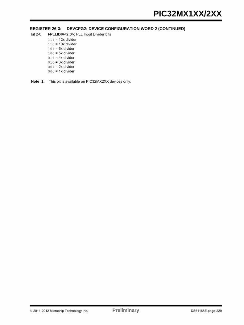
PIC32MX1XX/2XX
bit 2-0 FPLLIDIV<2:0>: PLL Input Divider bits
111 = 12x divider110 = 10x divider101 = 6x divider100 = 5x divider011 = 4x divider010 = 3x divider001 = 2x divider000 = 1x divider
REGISTER 26-3: DEVCFG2: DEVICE CONFIGURATION WORD 2 (CONTINUED)
Note 1: This bit is available on PIC32MX2XX devices only.
2011-2012 Microchip Technology Inc. Preliminary DS61168E-page 229
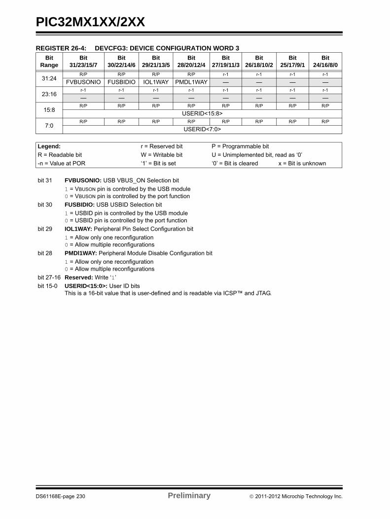
PIC32MX1XX/2XX
REGISTER 26-4: DEVCFG3: DEVICE CONFIGURATION WORD 3
Bit Range
Bit31/23/15/7
Bit30/22/14/6
Bit29/21/13/5
Bit28/20/12/4
Bit27/19/11/3
Bit26/18/10/2
Bit25/17/9/1
Bit24/16/8/0
31:24R/P R/P R/P R/P r-1 r-1 r-1 r-1
FVBUSONIO FUSBIDIO IOL1WAY PMDL1WAY — — — —
23:16r-1 r-1 r-1 r-1 r-1 r-1 r-1 r-1
— — — — — — — —
15:8R/P R/P R/P R/P R/P R/P R/P R/P
USERID<15:8>
7:0R/P R/P R/P R/P R/P R/P R/P R/P
USERID<7:0>
Legend: r = Reserved bit P = Programmable bit
R = Readable bit W = Writable bit U = Unimplemented bit, read as ‘0’
-n = Value at POR ‘1’ = Bit is set ‘0’ = Bit is cleared x = Bit is unknown
bit 31 FVBUSONIO: USB VBUS_ON Selection bit
1 = VBUSON pin is controlled by the USB module0 = VBUSON pin is controlled by the port function
bit 30 FUSBIDIO: USB USBID Selection bit
1 = USBID pin is controlled by the USB module0 = USBID pin is controlled by the port function
bit 29 IOL1WAY: Peripheral Pin Select Configuration bit
1 = Allow only one reconfiguration0 = Allow multiple reconfigurations
bit 28 PMDl1WAY: Peripheral Module Disable Configuration bit
1 = Allow only one reconfiguration0 = Allow multiple reconfigurations
bit 27-16 Reserved: Write ‘1’
bit 15-0 USERID<15:0>: User ID bitsThis is a 16-bit value that is user-defined and is readable via ICSP™ and JTAG.
DS61168E-page 230 Preliminary 2011-2012 Microchip Technology Inc.
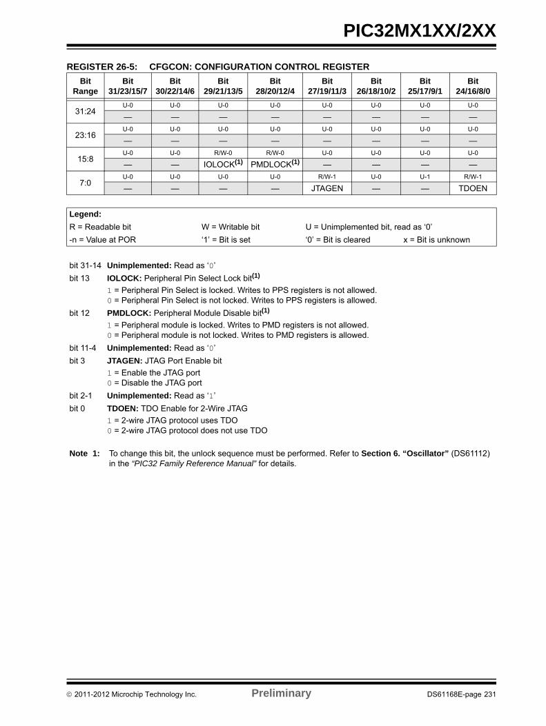
PIC32MX1XX/2XX
REGISTER 26-5: CFGCON: CONFIGURATION CONTROL REGISTER
Bit Range
Bit31/23/15/7
Bit30/22/14/6
Bit29/21/13/5
Bit28/20/12/4
Bit27/19/11/3
Bit26/18/10/2
Bit25/17/9/1
Bit24/16/8/0
31:24U-0 U-0 U-0 U-0 U-0 U-0 U-0 U-0
— — — — — — — —
23:16U-0 U-0 U-0 U-0 U-0 U-0 U-0 U-0
— — — — — — — —
15:8U-0 U-0 R/W-0 R/W-0 U-0 U-0 U-0 U-0
— — IOLOCK(1) PMDLOCK(1) — — — —
7:0U-0 U-0 U-0 U-0 R/W-1 U-0 U-1 R/W-1
— — — — JTAGEN — — TDOEN
Legend:
R = Readable bit W = Writable bit U = Unimplemented bit, read as ‘0’
-n = Value at POR ‘1’ = Bit is set ‘0’ = Bit is cleared x = Bit is unknown
bit 31-14 Unimplemented: Read as ‘0’
bit 13 IOLOCK: Peripheral Pin Select Lock bit(1)
1 = Peripheral Pin Select is locked. Writes to PPS registers is not allowed.0 = Peripheral Pin Select is not locked. Writes to PPS registers is allowed.
bit 12 PMDLOCK: Peripheral Module Disable bit(1)
1 = Peripheral module is locked. Writes to PMD registers is not allowed.0 = Peripheral module is not locked. Writes to PMD registers is allowed.
bit 11-4 Unimplemented: Read as ‘0’
bit 3 JTAGEN: JTAG Port Enable bit
1 = Enable the JTAG port0 = Disable the JTAG port
bit 2-1 Unimplemented: Read as ‘1’
bit 0 TDOEN: TDO Enable for 2-Wire JTAG
1 = 2-wire JTAG protocol uses TDO0 = 2-wire JTAG protocol does not use TDO
Note 1: To change this bit, the unlock sequence must be performed. Refer to Section 6. “Oscillator” (DS61112) in the “PIC32 Family Reference Manual” for details.
2011-2012 Microchip Technology Inc. Preliminary DS61168E-page 231
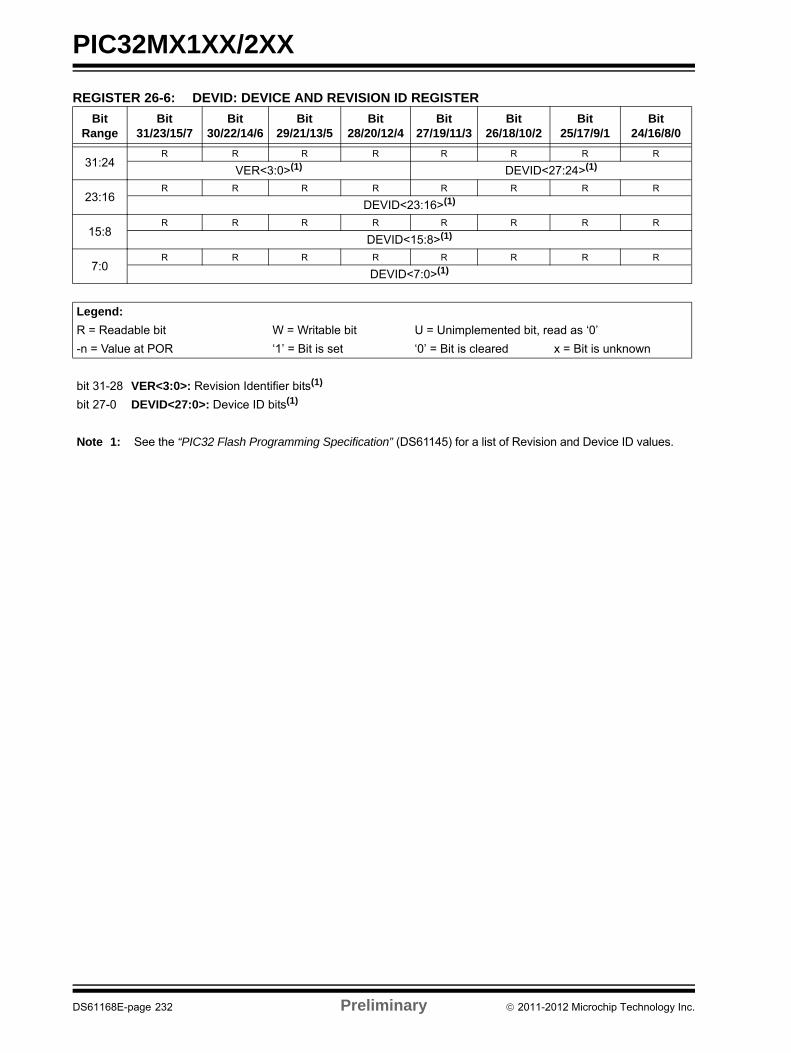
PIC32MX1XX/2XX
REGISTER 26-6: DEVID: DEVICE AND REVISION ID REGISTER
Bit Range
Bit31/23/15/7
Bit30/22/14/6
Bit29/21/13/5
Bit28/20/12/4
Bit27/19/11/3
Bit26/18/10/2
Bit25/17/9/1
Bit24/16/8/0
31:24R R R R R R R R
VER<3:0>(1) DEVID<27:24>(1)
23:16R R R R R R R R
DEVID<23:16>(1)
15:8R R R R R R R R
DEVID<15:8>(1)
7:0R R R R R R R R
DEVID<7:0>(1)
Legend:
R = Readable bit W = Writable bit U = Unimplemented bit, read as ‘0’
-n = Value at POR ‘1’ = Bit is set ‘0’ = Bit is cleared x = Bit is unknown
bit 31-28 VER<3:0>: Revision Identifier bits(1)
bit 27-0 DEVID<27:0>: Device ID bits(1)
Note 1: See the “PIC32 Flash Programming Specification” (DS61145) for a list of Revision and Device ID values.
DS61168E-page 232 Preliminary 2011-2012 Microchip Technology Inc.
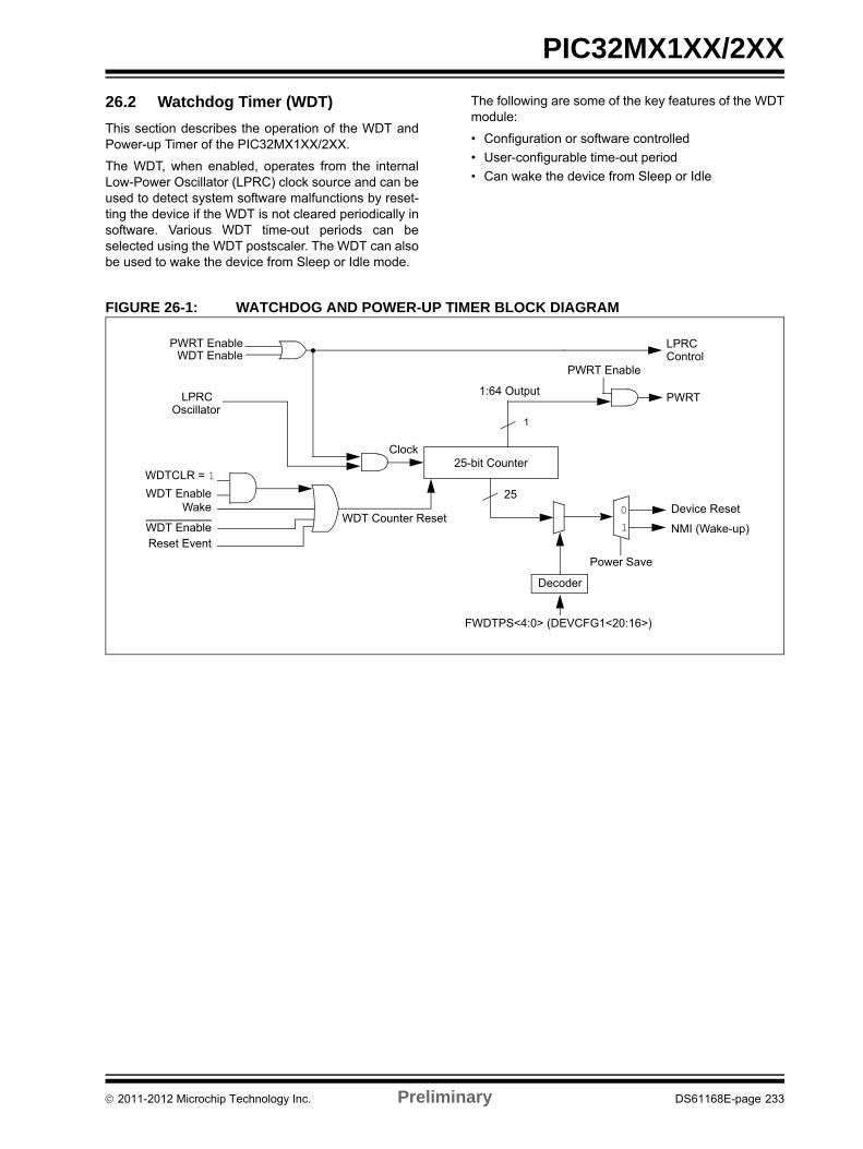
PIC32MX1XX/2XX
26.2 Watchdog Timer (WDT)
This section describes the operation of the WDT andPower-up Timer of the PIC32MX1XX/2XX.
The WDT, when enabled, operates from the internalLow-Power Oscillator (LPRC) clock source and can beused to detect system software malfunctions by reset-ting the device if the WDT is not cleared periodically insoftware. Various WDT time-out periods can beselected using the WDT postscaler. The WDT can alsobe used to wake the device from Sleep or Idle mode.
The following are some of the key features of the WDTmodule:
• Configuration or software controlled
• User-configurable time-out period
• Can wake the device from Sleep or Idle
FIGURE 26-1: WATCHDOG AND POWER-UP TIMER BLOCK DIAGRAM
Wake
WDTCLR = 1
WDT Enable
LPRC
Power Save
25-bit Counter
PWRT EnableWDT Enable
LPRC
WDT Counter Reset
Control
Oscillator
25Device Reset
NMI (Wake-up)
PWRT
PWRT Enable
FWDTPS<4:0> (DEVCFG1<20:16>)
Clock
Decoder
1
1:64 Output
0
1WDT EnableReset Event
2011-2012 Microchip Technology Inc. Preliminary DS61168E-page 233
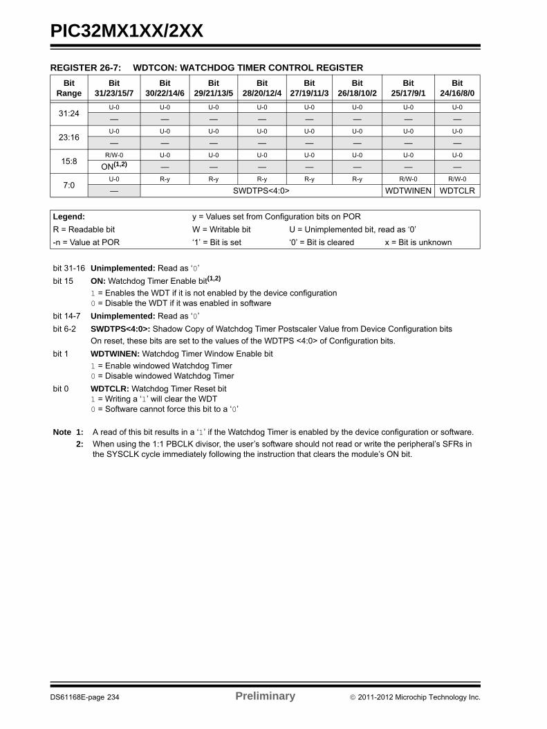
PIC32MX1XX/2XX
REGISTER 26-7: WDTCON: WATCHDOG TIMER CONTROL REGISTER
Bit Range
Bit31/23/15/7
Bit30/22/14/6
Bit29/21/13/5
Bit28/20/12/4
Bit27/19/11/3
Bit26/18/10/2
Bit25/17/9/1
Bit24/16/8/0
31:24U-0 U-0 U-0 U-0 U-0 U-0 U-0 U-0
— — — — — — — —
23:16U-0 U-0 U-0 U-0 U-0 U-0 U-0 U-0
— — — — — — — —
15:8R/W-0 U-0 U-0 U-0 U-0 U-0 U-0 U-0
ON(1,2) — — — — — — —
7:0U-0 R-y R-y R-y R-y R-y R/W-0 R/W-0
— SWDTPS<4:0> WDTWINEN WDTCLR
Legend: y = Values set from Configuration bits on POR
R = Readable bit W = Writable bit U = Unimplemented bit, read as ‘0’
-n = Value at POR ‘1’ = Bit is set ‘0’ = Bit is cleared x = Bit is unknown
bit 31-16 Unimplemented: Read as ‘0’
bit 15 ON: Watchdog Timer Enable bit(1,2)
1 = Enables the WDT if it is not enabled by the device configuration0 = Disable the WDT if it was enabled in software
bit 14-7 Unimplemented: Read as ‘0’
bit 6-2 SWDTPS<4:0>: Shadow Copy of Watchdog Timer Postscaler Value from Device Configuration bits
On reset, these bits are set to the values of the WDTPS <4:0> of Configuration bits.
bit 1 WDTWINEN: Watchdog Timer Window Enable bit
1 = Enable windowed Watchdog Timer0 = Disable windowed Watchdog Timer
bit 0 WDTCLR: Watchdog Timer Reset bit1 = Writing a ‘1’ will clear the WDT0 = Software cannot force this bit to a ‘0’
Note 1: A read of this bit results in a ‘1’ if the Watchdog Timer is enabled by the device configuration or software.
2: When using the 1:1 PBCLK divisor, the user’s software should not read or write the peripheral’s SFRs in the SYSCLK cycle immediately following the instruction that clears the module’s ON bit.
DS61168E-page 234 Preliminary 2011-2012 Microchip Technology Inc.
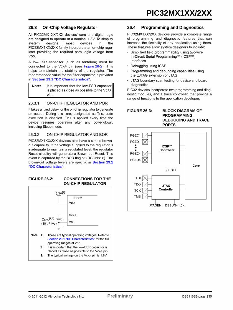
PIC32MX1XX/2XX
26.3 On-Chip Voltage Regulator
All PIC32MX1XX/2XX devices’ core and digital logicare designed to operate at a nominal 1.8V. To simplifysystem designs, most devices in thePIC32MX1XX/2XX family incorporate an on-chip regu-lator providing the required core logic voltage fromVDD.
A low-ESR capacitor (such as tantalum) must beconnected to the VCAP pin (see Figure 26-2). Thishelps to maintain the stability of the regulator. Therecommended value for the filter capacitor is providedin Section 29.1 “DC Characteristics”.
26.3.1 ON-CHIP REGULATOR AND POR
It takes a fixed delay for the on-chip regulator to generatean output. During this time, designated as TPU, codeexecution is disabled. TPU is applied every time thedevice resumes operation after any power-down,including Sleep mode.
26.3.2 ON-CHIP REGULATOR AND BOR
PIC32MX1XX/2XX devices also have a simple brown-out capability. If the voltage supplied to the regulator isinadequate to maintain a regulated level, the regulatorReset circuitry will generate a Brown-out Reset. Thisevent is captured by the BOR flag bit (RCON<1>). Thebrown-out voltage levels are specific in Section 29.1“DC Characteristics”.
FIGURE 26-2: CONNECTIONS FOR THE ON-CHIP REGULATOR
26.4 Programming and Diagnostics
PIC32MX1XX/2XX devices provide a complete rangeof programming and diagnostic features that canincrease the flexibility of any application using them.These features allow system designers to include:
• Simplified field programmability using two-wire In-Circuit Serial Programming™ (ICSP™) interfaces
• Debugging using ICSP
• Programming and debugging capabilities using the EJTAG extension of JTAG
• JTAG boundary scan testing for device and board diagnostics
PIC32 devices incorporate two programming and diag-nostic modules, and a trace controller, that provide arange of functions to the application developer.
FIGURE 26-3: BLOCK DIAGRAM OF PROGRAMMING, DEBUGGING AND TRACE PORTS
Note: It is important that the low-ESR capacitoris placed as close as possible to the VCAP
pin.
VDD
VCAP
VSS
PIC32
CEFC(2,3)
3.3V(1)
Note 1: These are typical operating voltages. Refer to Section 29.1 “DC Characteristics” for the full operating ranges of VDD.
2: It is important that the low-ESR capacitor is placed as close as possible to the VCAP pin.
3: The typical voltage on the VCAP pin is 1.8V.
(10 F typ)
TDI
TDO
TCK
TMS
JTAGController
ICSP™Controller
Core
JTAGEN DEBUG<1:0>
ICESEL
PGEC1
PGED1
PGEC4
PGED4
2011-2012 Microchip Technology Inc. Preliminary DS61168E-page 235

PIC32MX1XX/2XX
NOTES:
DS61168E-page 236 Preliminary 2011-2012 Microchip Technology Inc.
PIC32MX1XX/2XX
27.0 INSTRUCTION SET
The PIC32MX1XX/2XX family instruction set complieswith the MIPS32® Release 2 instruction set architec-ture. The PIC32 device family does not support the fol-lowing features:
• Core extend instructions
• Coprocessor 1 instructions
• Coprocessor 2 instructions
Note: Refer to “MIPS32® Architecture forProgrammers Volume II: The MIPS32®
Instruction Set” at www.mips.com formore information.
2011-2012 Microchip Technology Inc. Preliminary DS61168E-page 237

PIC32MX1XX/2XX
NOTES:
DS61168E-page 238 Preliminary 2011-2012 Microchip Technology Inc.
PIC32MX1XX/2XX
28.0 DEVELOPMENT SUPPORT
The PIC® microcontrollers and dsPIC® digital signalcontrollers are supported with a full range of softwareand hardware development tools:
• Integrated Development Environment
- MPLAB® IDE Software
• Compilers/Assemblers/Linkers
- MPLAB C Compiler for Various DeviceFamilies
- HI-TECH C® for Various Device Families
- MPASMTM Assembler
- MPLINKTM Object Linker/MPLIBTM Object Librarian
- MPLAB Assembler/Linker/Librarian forVarious Device Families
• Simulators
- MPLAB SIM Software Simulator
• Emulators
- MPLAB REAL ICE™ In-Circuit Emulator
• In-Circuit Debuggers
- MPLAB ICD 3
- PICkit™ 3 Debug Express
• Device Programmers
- PICkit™ 2 Programmer
- MPLAB PM3 Device Programmer
• Low-Cost Demonstration/Development Boards, Evaluation Kits, and Starter Kits
28.1 MPLAB Integrated Development Environment Software
The MPLAB IDE software brings an ease of softwaredevelopment previously unseen in the 8/16/32-bitmicrocontroller market. The MPLAB IDE is a Windows®
operating system-based application that contains:
• A single graphical interface to all debugging tools
- Simulator
- Programmer (sold separately)
- In-Circuit Emulator (sold separately)
- In-Circuit Debugger (sold separately)
• A full-featured editor with color-coded context
• A multiple project manager
• Customizable data windows with direct edit of contents
• High-level source code debugging
• Mouse over variable inspection
• Drag and drop variables from source to watch windows
• Extensive on-line help
• Integration of select third party tools, such as IAR C Compilers
The MPLAB IDE allows you to:
• Edit your source files (either C or assembly)
• One-touch compile or assemble, and download to emulator and simulator tools (automatically updates all project information)
• Debug using:
- Source files (C or assembly)
- Mixed C and assembly
- Machine code
MPLAB IDE supports multiple debugging tools in asingle development paradigm, from the cost-effectivesimulators, through low-cost in-circuit debuggers, tofull-featured emulators. This eliminates the learningcurve when upgrading to tools with increased flexibilityand power.
2011-2012 Microchip Technology Inc. Preliminary DS61168E-page 239
PIC32MX1XX/2XX
28.2 MPLAB C Compilers for Various Device Families
The MPLAB C Compiler code development systemsare complete ANSI C compilers for Microchip’s PIC18,PIC24 and PIC32 families of microcontrollers and thedsPIC30 and dsPIC33 families of digital signal control-lers. These compilers provide powerful integrationcapabilities, superior code optimization and ease ofuse.
For easy source level debugging, the compilers providesymbol information that is optimized to the MPLAB IDEdebugger.
28.3 HI-TECH C for Various Device Families
The HI-TECH C Compiler code development systemsare complete ANSI C compilers for Microchip’s PICfamily of microcontrollers and the dsPIC family of digitalsignal controllers. These compilers provide powerfulintegration capabilities, omniscient code generationand ease of use.
For easy source level debugging, the compilers providesymbol information that is optimized to the MPLAB IDEdebugger.
The compilers include a macro assembler, linker, pre-processor, and one-step driver, and can run on multipleplatforms.
28.4 MPASM Assembler
The MPASM Assembler is a full-featured, universalmacro assembler for PIC10/12/16/18 MCUs.
The MPASM Assembler generates relocatable objectfiles for the MPLINK Object Linker, Intel® standard HEXfiles, MAP files to detail memory usage and symbolreference, absolute LST files that contain source linesand generated machine code and COFF files fordebugging.
The MPASM Assembler features include:
• Integration into MPLAB IDE projects
• User-defined macros to streamline assembly code
• Conditional assembly for multi-purpose source files
• Directives that allow complete control over the assembly process
28.5 MPLINK Object Linker/MPLIB Object Librarian
The MPLINK Object Linker combines relocatableobjects created by the MPASM Assembler and theMPLAB C18 C Compiler. It can link relocatable objectsfrom precompiled libraries, using directives from alinker script.
The MPLIB Object Librarian manages the creation andmodification of library files of precompiled code. Whena routine from a library is called from a source file, onlythe modules that contain that routine will be linked inwith the application. This allows large libraries to beused efficiently in many different applications.
The object linker/library features include:
• Efficient linking of single libraries instead of many smaller files
• Enhanced code maintainability by grouping related modules together
• Flexible creation of libraries with easy module listing, replacement, deletion and extraction
28.6 MPLAB Assembler, Linker and Librarian for Various Device Families
MPLAB Assembler produces relocatable machinecode from symbolic assembly language for PIC24,PIC32 and dsPIC devices. MPLAB C Compiler usesthe assembler to produce its object file. The assemblergenerates relocatable object files that can then bearchived or linked with other relocatable object files andarchives to create an executable file. Notable featuresof the assembler include:
• Support for the entire device instruction set
• Support for fixed-point and floating-point data
• Command line interface
• Rich directive set
• Flexible macro language
• MPLAB IDE compatibility
DS61168E-page 240 Preliminary 2011-2012 Microchip Technology Inc.
PIC32MX1XX/2XX
28.7 MPLAB SIM Software Simulator
The MPLAB SIM Software Simulator allows codedevelopment in a PC-hosted environment by simulat-ing the PIC MCUs and dsPIC® DSCs on an instructionlevel. On any given instruction, the data areas can beexamined or modified and stimuli can be applied froma comprehensive stimulus controller. Registers can belogged to files for further run-time analysis. The tracebuffer and logic analyzer display extend the power ofthe simulator to record and track program execution,actions on I/O, most peripherals and internal registers.
The MPLAB SIM Software Simulator fully supportssymbolic debugging using the MPLAB C Compilers,and the MPASM and MPLAB Assemblers. The soft-ware simulator offers the flexibility to develop anddebug code outside of the hardware laboratory envi-ronment, making it an excellent, economical softwaredevelopment tool.
28.8 MPLAB REAL ICE In-Circuit Emulator System
MPLAB REAL ICE In-Circuit Emulator System isMicrochip’s next generation high-speed emulator forMicrochip Flash DSC and MCU devices. It debugs andprograms PIC® Flash MCUs and dsPIC® Flash DSCswith the easy-to-use, powerful graphical user interface ofthe MPLAB Integrated Development Environment (IDE),included with each kit.
The emulator is connected to the design engineer’s PCusing a high-speed USB 2.0 interface and is connectedto the target with either a connector compatible with in-circuit debugger systems (RJ11) or with the new high-speed, noise tolerant, Low-Voltage Differential Signal(LVDS) interconnection (CAT5).
The emulator is field upgradable through future firmwaredownloads in MPLAB IDE. In upcoming releases ofMPLAB IDE, new devices will be supported, and newfeatures will be added. MPLAB REAL ICE offerssignificant advantages over competitive emulatorsincluding low-cost, full-speed emulation, run-timevariable watches, trace analysis, complex breakpoints, aruggedized probe interface and long (up to three meters)interconnection cables.
28.9 MPLAB ICD 3 In-Circuit Debugger System
MPLAB ICD 3 In-Circuit Debugger System is Micro-chip's most cost effective high-speed hardwaredebugger/programmer for Microchip Flash Digital Sig-nal Controller (DSC) and microcontroller (MCU)devices. It debugs and programs PIC® Flash microcon-trollers and dsPIC® DSCs with the powerful, yet easy-to-use graphical user interface of MPLAB IntegratedDevelopment Environment (IDE).
The MPLAB ICD 3 In-Circuit Debugger probe is con-nected to the design engineer's PC using a high-speedUSB 2.0 interface and is connected to the target with aconnector compatible with the MPLAB ICD 2 or MPLABREAL ICE systems (RJ-11). MPLAB ICD 3 supports allMPLAB ICD 2 headers.
28.10 PICkit 3 In-Circuit Debugger/Programmer and PICkit 3 Debug Express
The MPLAB PICkit 3 allows debugging and program-ming of PIC® and dsPIC® Flash microcontrollers at amost affordable price point using the powerful graphicaluser interface of the MPLAB Integrated DevelopmentEnvironment (IDE). The MPLAB PICkit 3 is connectedto the design engineer's PC using a full speed USBinterface and can be connected to the target via anMicrochip debug (RJ-11) connector (compatible withMPLAB ICD 3 and MPLAB REAL ICE). The connectoruses two device I/O pins and the reset line to imple-ment in-circuit debugging and In-Circuit Serial Pro-gramming™.
The PICkit 3 Debug Express include the PICkit 3, demoboard and microcontroller, hookup cables and CDROMwith user’s guide, lessons, tutorial, compiler andMPLAB IDE software.
2011-2012 Microchip Technology Inc. Preliminary DS61168E-page 241
PIC32MX1XX/2XX
28.11 PICkit 2 Development Programmer/Debugger and PICkit 2 Debug Express
The PICkit™ 2 Development Programmer/Debugger isa low-cost development tool with an easy to use inter-face for programming and debugging Microchip’s Flashfamilies of microcontrollers. The full featuredWindows® programming interface supports baseline(PIC10F, PIC12F5xx, PIC16F5xx), midrange(PIC12F6xx, PIC16F), PIC18F, PIC24, dsPIC30,dsPIC33, and PIC32 families of 8-bit, 16-bit, and 32-bitmicrocontrollers, and many Microchip Serial EEPROMproducts. With Microchip’s powerful MPLAB IntegratedDevelopment Environment (IDE) the PICkit™ 2enables in-circuit debugging on most PIC® microcon-trollers. In-Circuit-Debugging runs, halts and singlesteps the program while the PIC microcontroller isembedded in the application. When halted at a break-point, the file registers can be examined and modified.
The PICkit 2 Debug Express include the PICkit 2, demoboard and microcontroller, hookup cables and CDROMwith user’s guide, lessons, tutorial, compiler andMPLAB IDE software.
28.12 MPLAB PM3 Device Programmer
The MPLAB PM3 Device Programmer is a universal,CE compliant device programmer with programmablevoltage verification at VDDMIN and VDDMAX formaximum reliability. It features a large LCD display(128 x 64) for menus and error messages and a modu-lar, detachable socket assembly to support variouspackage types. The ICSP™ cable assembly is includedas a standard item. In Stand-Alone mode, the MPLABPM3 Device Programmer can read, verify and programPIC devices without a PC connection. It can also setcode protection in this mode. The MPLAB PM3connects to the host PC via an RS-232 or USB cable.The MPLAB PM3 has high-speed communications andoptimized algorithms for quick programming of largememory devices and incorporates an MMC card for filestorage and data applications.
28.13 Demonstration/Development Boards, Evaluation Kits, and Starter Kits
A wide variety of demonstration, development andevaluation boards for various PIC MCUs and dsPICDSCs allows quick application development on fully func-tional systems. Most boards include prototyping areas foradding custom circuitry and provide application firmwareand source code for examination and modification.
The boards support a variety of features, including LEDs,temperature sensors, switches, speakers, RS-232interfaces, LCD displays, potentiometers and additionalEEPROM memory.
The demonstration and development boards can beused in teaching environments, for prototyping customcircuits and for learning about various microcontrollerapplications.
In addition to the PICDEM™ and dsPICDEM™ demon-stration/development board series of circuits, Microchiphas a line of evaluation kits and demonstration softwarefor analog filter design, KEELOQ® security ICs, CAN,IrDA®, PowerSmart battery management, SEEVAL®
evaluation system, Sigma-Delta ADC, flow ratesensing, plus many more.
Also available are starter kits that contain everythingneeded to experience the specified device. This usuallyincludes a single application and debug capability, allon one board.
Check the Microchip web page (www.microchip.com)for the complete list of demonstration, developmentand evaluation kits.
DS61168E-page 242 Preliminary 2011-2012 Microchip Technology Inc.
PIC32MX1XX/2XX
29.0 ELECTRICAL CHARACTERISTICS
This section provides an overview of the PIC32MX1XX/2XX electrical characteristics. Additional information will beprovided in future revisions of this document as it becomes available.
Absolute maximum ratings for the PIC32MX1XX/2XX devices are listed below. Exposure to these maximum ratingconditions for extended periods may affect device reliability. Functional operation of the device at these or any otherconditions, above the parameters indicated in the operation listings of this specification, is not implied.
Absolute Maximum Ratings(See Note 1)
Ambient temperature under bias............................................................................................................ .-40°C to +105°C
Storage temperature .............................................................................................................................. -65°C to +150°C
Voltage on VDD with respect to VSS ......................................................................................................... -0.3V to +4.0V
Voltage on any pin that is not 5V tolerant, with respect to VSS (Note 3)......................................... -0.3V to (VDD + 0.3V)
Voltage on any 5V tolerant pin with respect to VSS when VDD 2.3V (Note 3) ........................................ -0.3V to +5.5V
Voltage on any 5V tolerant pin with respect to VSS when VDD < 2.3V (Note 3)........................................ -0.3V to +3.6V
Voltage on D+ or D- pin with respect to VUSB3V3 ..................................................................... -0.3V to (VUSB3V3 + 0.3V)
Voltage on VBUS with respect to VSS ....................................................................................................... -0.3V to +5.5V
Maximum current out of VSS pin(s) .......................................................................................................................300 mA
Maximum current into VDD pin(s) (Note 2)............................................................................................................300 mA
Maximum output current sunk by any I/O pin..........................................................................................................15 mA
Maximum output current sourced by any I/O pin ....................................................................................................15 mA
Maximum current sunk by all ports .......................................................................................................................200 mA
Maximum current sourced by all ports (Note 2)....................................................................................................200 mA
Note 1: Stresses above those listed under “Absolute Maximum Ratings” may cause permanent damage to thedevice. This is a stress rating only and functional operation of the device at those or any other conditions,above those indicated in the operation listings of this specification, is not implied. Exposure to maximumrating conditions for extended periods may affect device reliability.
2: Maximum allowable current is a function of device maximum power dissipation (see Table 29-2).
3: See the “Pin Diagrams” section for the 5V tolerant pins.
2011-2012 Microchip Technology Inc. Preliminary DS61168E-page 243
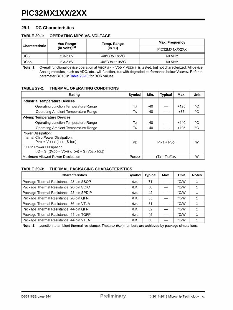
PIC32MX1XX/2XX
29.1 DC Characteristics
TABLE 29-1: OPERATING MIPS VS. VOLTAGE
CharacteristicVDD Range(in Volts)(1)
Temp. Range(in °C)
Max. Frequency
PIC32MX1XX/2XX
DC5 2.3-3.6V -40°C to +85°C 40 MHz
DC5b 2.3-3.6V -40°C to +105°C 40 MHz
Note 1: Overall functional device operation at VBORMIN < VDD < VDDMIN is tested, but not characterized. All device Analog modules, such as ADC, etc., will function, but with degraded performance below VDDMIN. Refer to parameter BO10 in Table 29-10 for BOR values.
TABLE 29-2: THERMAL OPERATING CONDITIONS
Rating Symbol Min. Typical Max. Unit
Industrial Temperature Devices
Operating Junction Temperature Range TJ -40 — +125 °C
Operating Ambient Temperature Range TA -40 — +85 °C
V-temp Temperature Devices
Operating Junction Temperature Range TJ -40 — +140 °C
Operating Ambient Temperature Range TA -40 — +105 °C
Power Dissipation:Internal Chip Power Dissipation:
PINT = VDD x (IDD – S IOH) PD PINT + PI/O WI/O Pin Power Dissipation:
I/O = S (({VDD – VOH} x IOH) + S (VOL x IOL))
Maximum Allowed Power Dissipation PDMAX (TJ – TA)/JA W
TABLE 29-3: THERMAL PACKAGING CHARACTERISTICS
Characteristics Symbol Typical Max. Unit Notes
Package Thermal Resistance, 28-pin SSOP JA 71 — °C/W 1
Package Thermal Resistance, 28-pin SOIC JA 50 — °C/W 1
Package Thermal Resistance, 28-pin SPDIP JA 42 — °C/W 1
Package Thermal Resistance, 28-pin QFN JA 35 — °C/W 1
Package Thermal Resistance, 36-pin VTLA JA 31 — °C/W 1
Package Thermal Resistance, 44-pin QFN JA 32 — °C/W 1
Package Thermal Resistance, 44-pin TQFP JA 45 — °C/W 1
Package Thermal Resistance, 44-pin VTLA JA 30 — °C/W 1
Note 1: Junction to ambient thermal resistance, Theta-JA (JA) numbers are achieved by package simulations.
DS61168E-page 244 Preliminary 2011-2012 Microchip Technology Inc.
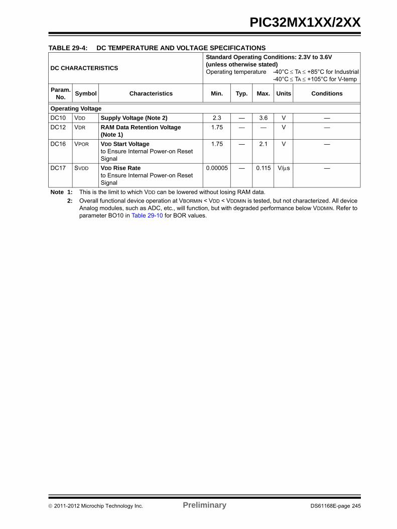
PIC32MX1XX/2XX
TABLE 29-4: DC TEMPERATURE AND VOLTAGE SPECIFICATIONS
DC CHARACTERISTICS
Standard Operating Conditions: 2.3V to 3.6V(unless otherwise stated)Operating temperature -40°C TA +85°C for Industrial
-40°C TA +105°C for V-temp
Param. No.
Symbol Characteristics Min. Typ. Max. Units Conditions
Operating Voltage
DC10 VDD Supply Voltage (Note 2) 2.3 — 3.6 V —
DC12 VDR RAM Data Retention Voltage (Note 1)
1.75 — — V —
DC16 VPOR VDD Start Voltageto Ensure Internal Power-on Reset Signal
1.75 — 2.1 V —
DC17 SVDD VDD Rise Rateto Ensure Internal Power-on Reset Signal
0.00005 — 0.115 V/s —
Note 1: This is the limit to which VDD can be lowered without losing RAM data.
2: Overall functional device operation at VBORMIN < VDD < VDDMIN is tested, but not characterized. All device Analog modules, such as ADC, etc., will function, but with degraded performance below VDDMIN. Refer to parameter BO10 in Table 29-10 for BOR values.
2011-2012 Microchip Technology Inc. Preliminary DS61168E-page 245
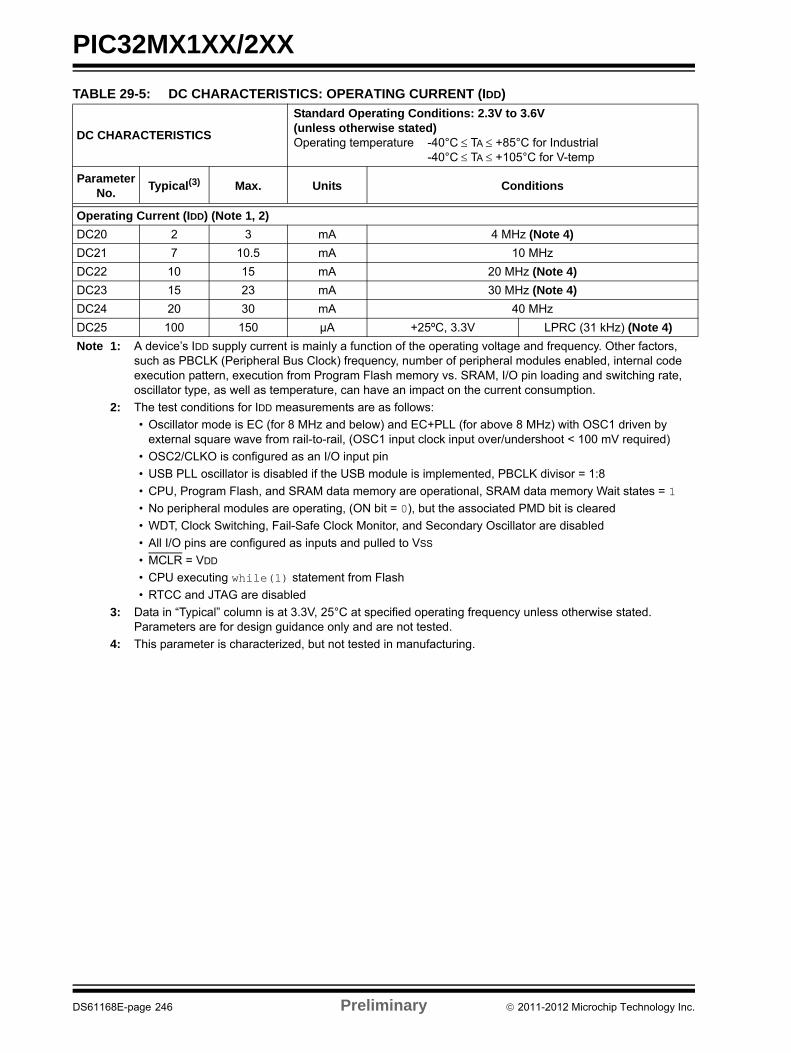
PIC32MX1XX/2XX
TABLE 29-5: DC CHARACTERISTICS: OPERATING CURRENT (IDD)
DC CHARACTERISTICS
Standard Operating Conditions: 2.3V to 3.6V(unless otherwise stated)Operating temperature -40°C TA +85°C for Industrial
-40°C TA +105°C for V-temp
Parameter No.
Typical(3) Max. Units Conditions
Operating Current (IDD) (Note 1, 2)
DC20 2 3 mA 4 MHz (Note 4)
DC21 7 10.5 mA 10 MHz
DC22 10 15 mA 20 MHz (Note 4)
DC23 15 23 mA 30 MHz (Note 4)
DC24 20 30 mA 40 MHz
DC25 100 150 µA +25ºC, 3.3V LPRC (31 kHz) (Note 4)
Note 1: A device’s IDD supply current is mainly a function of the operating voltage and frequency. Other factors, such as PBCLK (Peripheral Bus Clock) frequency, number of peripheral modules enabled, internal code execution pattern, execution from Program Flash memory vs. SRAM, I/O pin loading and switching rate, oscillator type, as well as temperature, can have an impact on the current consumption.
2: The test conditions for IDD measurements are as follows:
• Oscillator mode is EC (for 8 MHz and below) and EC+PLL (for above 8 MHz) with OSC1 driven by external square wave from rail-to-rail, (OSC1 input clock input over/undershoot < 100 mV required)
• OSC2/CLKO is configured as an I/O input pin
• USB PLL oscillator is disabled if the USB module is implemented, PBCLK divisor = 1:8
• CPU, Program Flash, and SRAM data memory are operational, SRAM data memory Wait states = 1
• No peripheral modules are operating, (ON bit = 0), but the associated PMD bit is cleared
• WDT, Clock Switching, Fail-Safe Clock Monitor, and Secondary Oscillator are disabled
• All I/O pins are configured as inputs and pulled to VSS
• MCLR = VDD
• CPU executing while(1) statement from Flash
• RTCC and JTAG are disabled
3: Data in “Typical” column is at 3.3V, 25°C at specified operating frequency unless otherwise stated. Parameters are for design guidance only and are not tested.
4: This parameter is characterized, but not tested in manufacturing.
DS61168E-page 246 Preliminary 2011-2012 Microchip Technology Inc.
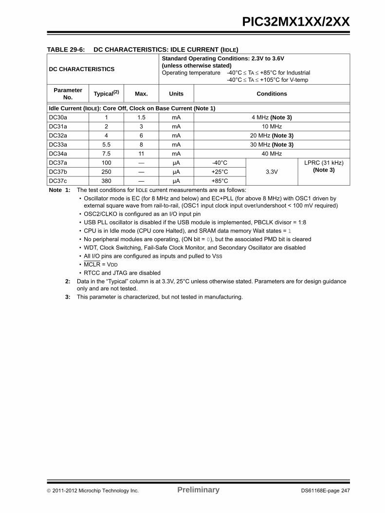
PIC32MX1XX/2XX
TABLE 29-6: DC CHARACTERISTICS: IDLE CURRENT (IIDLE)
DC CHARACTERISTICS
Standard Operating Conditions: 2.3V to 3.6V(unless otherwise stated)Operating temperature -40°C TA +85°C for Industrial
-40°C TA +105°C for V-temp
Parameter No.
Typical(2) Max. Units Conditions
Idle Current (IIDLE): Core Off, Clock on Base Current (Note 1)
DC30a 1 1.5 mA 4 MHz (Note 3)
DC31a 2 3 mA 10 MHz
DC32a 4 6 mA 20 MHz (Note 3)
DC33a 5.5 8 mA 30 MHz (Note 3)
DC34a 7.5 11 mA 40 MHz
DC37a 100 — µA -40°C
3.3V
LPRC (31 kHz) (Note 3)DC37b 250 — µA +25°C
DC37c 380 — µA +85°C
Note 1: The test conditions for IIDLE current measurements are as follows:
• Oscillator mode is EC (for 8 MHz and below) and EC+PLL (for above 8 MHz) with OSC1 driven by external square wave from rail-to-rail, (OSC1 input clock input over/undershoot < 100 mV required)
• OSC2/CLKO is configured as an I/O input pin
• USB PLL oscillator is disabled if the USB module is implemented, PBCLK divisor = 1:8
• CPU is in Idle mode (CPU core Halted), and SRAM data memory Wait states = 1
• No peripheral modules are operating, (ON bit = 0), but the associated PMD bit is cleared
• WDT, Clock Switching, Fail-Safe Clock Monitor, and Secondary Oscillator are disabled
• All I/O pins are configured as inputs and pulled to VSS
• MCLR = VDD
• RTCC and JTAG are disabled
2: Data in the “Typical” column is at 3.3V, 25°C unless otherwise stated. Parameters are for design guidance only and are not tested.
3: This parameter is characterized, but not tested in manufacturing.
2011-2012 Microchip Technology Inc. Preliminary DS61168E-page 247
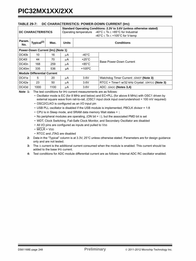
PIC32MX1XX/2XX
TABLE 29-7: DC CHARACTERISTICS: POWER-DOWN CURRENT (IPD)
DC CHARACTERISTICSStandard Operating Conditions: 2.3V to 3.6V (unless otherwise stated)Operating temperature -40°C TA +85°C for Industrial
-40°C TA +105°C for V-temp
Param. No.
Typical(2) Max. Units Conditions
Power-Down Current (IPD) (Note 1)
DC40k 10 16 A -40°C
Base Power-Down CurrentDC40l 44 70 A +25°C
DC40n 168 259 A +85°C
DC40m 335 536 µA +105ºC
Module Differential Current
DC41e 5 20 A 3.6V Watchdog Timer Current: IWDT (Note 3)
DC42e 23 50 A 3.6V RTCC + Timer1 w/32 kHz Crystal: IRTCC (Note 3)
DC43d 1000 1100 A 3.6V ADC: IADC (Notes 3,4)
Note 1: The test conditions for IPD current measurements are as follows:• Oscillator mode is EC (for 8 MHz and below) and EC+PLL (for above 8 MHz) with OSC1 driven by
external square wave from rail-to-rail, (OSC1 input clock input over/undershoot < 100 mV required)
• OSC2/CLKO is configured as an I/O input pin
• USB PLL oscillator is disabled if the USB module is implemented, PBCLK divisor = 1:8
• CPU is in Sleep mode, and SRAM data memory Wait states = 1
• No peripheral modules are operating, (ON bit = 0), but the associated PMD bit is set
• WDT, Clock Switching, Fail-Safe Clock Monitor, and Secondary Oscillator are disabled
• All I/O pins are configured as inputs and pulled to VSS
• MCLR = VDD
• RTCC and JTAG are disabled
2: Data in the “Typical” column is at 3.3V, 25°C unless otherwise stated. Parameters are for design guidance only and are not tested.
3: The current is the additional current consumed when the module is enabled. This current should be added to the base IPD current.
4: Test conditions for ADC module differential current are as follows: Internal ADC RC oscillator enabled.
DS61168E-page 248 Preliminary 2011-2012 Microchip Technology Inc.
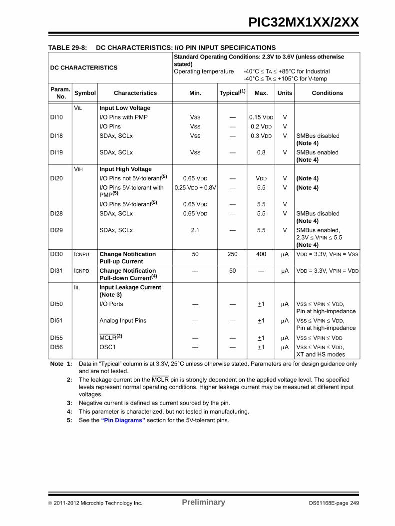
PIC32MX1XX/2XX
TABLE 29-8: DC CHARACTERISTICS: I/O PIN INPUT SPECIFICATIONS
DC CHARACTERISTICS
Standard Operating Conditions: 2.3V to 3.6V (unless otherwise stated)Operating temperature -40°C TA +85°C for Industrial
-40°C TA +105°C for V-temp
Param. No.
Symbol Characteristics Min. Typical(1) Max. Units Conditions
VIL Input Low Voltage
DI10 I/O Pins with PMP VSS — 0.15 VDD V
I/O Pins VSS — 0.2 VDD V
DI18 SDAx, SCLx VSS — 0.3 VDD V SMBus disabled (Note 4)
DI19 SDAx, SCLx VSS — 0.8 V SMBus enabled (Note 4)
VIH Input High Voltage
DI20 I/O Pins not 5V-tolerant(5) 0.65 VDD — VDD V (Note 4)
I/O Pins 5V-tolerant with PMP(5)
0.25 VDD + 0.8V — 5.5 V (Note 4)
I/O Pins 5V-tolerant(5) 0.65 VDD — 5.5 V
DI28 SDAx, SCLx 0.65 VDD — 5.5 V SMBus disabled (Note 4)
DI29 SDAx, SCLx 2.1 — 5.5 V SMBus enabled, 2.3V VPIN 5.5 (Note 4)
DI30 ICNPU Change Notification Pull-up Current
50 250 400 A VDD = 3.3V, VPIN = VSS
DI31 ICNPD Change Notification Pull-down Current(4)
— 50 — µA VDD = 3.3V, VPIN = VDD
IIL Input Leakage Current (Note 3)
DI50 I/O Ports — — +1 A VSS VPIN VDD,Pin at high-impedance
DI51 Analog Input Pins — — +1 A VSS VPIN VDD,Pin at high-impedance
DI55 MCLR(2) — — +1 A VSS VPIN VDD
DI56 OSC1 — — +1 A VSS VPIN VDD, XT and HS modes
Note 1: Data in “Typical” column is at 3.3V, 25°C unless otherwise stated. Parameters are for design guidance only and are not tested.
2: The leakage current on the MCLR pin is strongly dependent on the applied voltage level. The specified levels represent normal operating conditions. Higher leakage current may be measured at different input voltages.
3: Negative current is defined as current sourced by the pin.
4: This parameter is characterized, but not tested in manufacturing.
5: See the “Pin Diagrams” section for the 5V-tolerant pins.
2011-2012 Microchip Technology Inc. Preliminary DS61168E-page 249
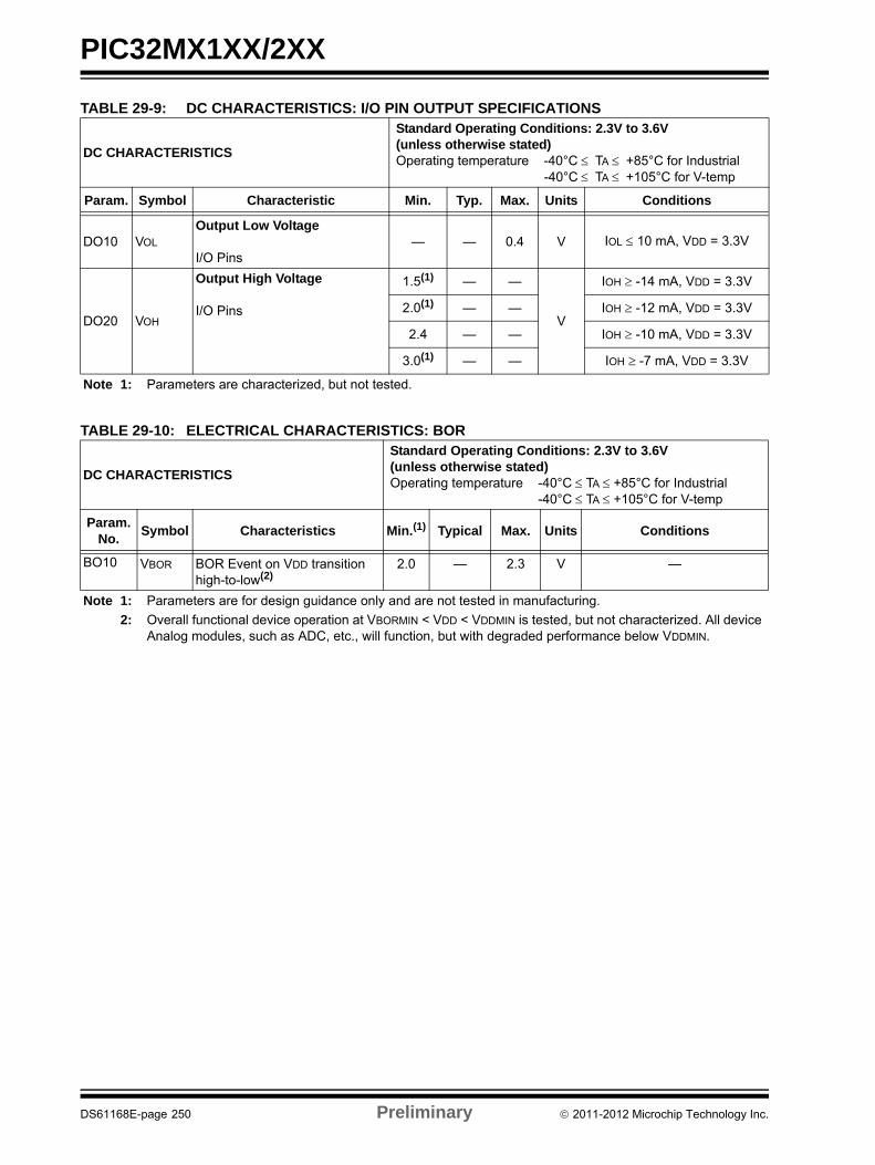
PIC32MX1XX/2XX
TABLE 29-9: DC CHARACTERISTICS: I/O PIN OUTPUT SPECIFICATIONS
DC CHARACTERISTICS
Standard Operating Conditions: 2.3V to 3.6V(unless otherwise stated)Operating temperature -40°C TA +85°C for Industrial
-40°C TA +105°C for V-temp
Param. Symbol Characteristic Min. Typ. Max. Units Conditions
DO10 VOL
Output Low Voltage
I/O Pins— — 0.4 V IOL 10 mA, VDD = 3.3V
DO20 VOH
Output High Voltage
I/O Pins
1.5(1) — —
V
IOH -14 mA, VDD = 3.3V
2.0(1) — — IOH -12 mA, VDD = 3.3V
2.4 — — IOH -10 mA, VDD = 3.3V
3.0(1) — — IOH -7 mA, VDD = 3.3V
Note 1: Parameters are characterized, but not tested.
TABLE 29-10: ELECTRICAL CHARACTERISTICS: BOR
DC CHARACTERISTICS
Standard Operating Conditions: 2.3V to 3.6V(unless otherwise stated)Operating temperature -40°C TA +85°C for Industrial
-40°C TA +105°C for V-temp
Param.No.
Symbol Characteristics Min.(1) Typical Max. Units Conditions
BO10 VBOR BOR Event on VDD transition high-to-low(2)
2.0 — 2.3 V —
Note 1: Parameters are for design guidance only and are not tested in manufacturing.
2: Overall functional device operation at VBORMIN < VDD < VDDMIN is tested, but not characterized. All device Analog modules, such as ADC, etc., will function, but with degraded performance below VDDMIN.
DS61168E-page 250 Preliminary 2011-2012 Microchip Technology Inc.
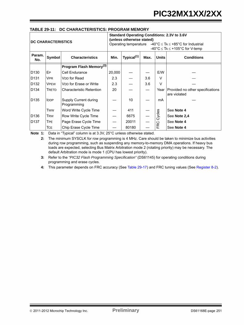
PIC32MX1XX/2XX
TABLE 29-11: DC CHARACTERISTICS: PROGRAM MEMORY
DC CHARACTERISTICS
Standard Operating Conditions: 2.3V to 3.6V(unless otherwise stated)Operating temperature -40°C TA +85°C for Industrial
-40°C TA +105°C for V-temp
Param.No.
Symbol Characteristics Min. Typical(1) Max. Units Conditions
Program Flash Memory(3)
D130 EP Cell Endurance 20,000 — — E/W —
D131 VPR VDD for Read 2.3 — 3.6 V —
D132 VPEW VDD for Erase or Write 2.3 — 3.6 V —
D134 TRETD Characteristic Retention 20 — — Year Provided no other specifications are violated
D135 IDDP Supply Current during Programming
— 10 — mA —
TWW Word Write Cycle Time — 411 —
FR
C C
ycle
s See Note 4
D136 TRW Row Write Cycle Time — 6675 — See Note 2,4
D137 TPE Page Erase Cycle Time — 20011 — See Note 4
TCE Chip Erase Cycle Time — 80180 — See Note 4
Note 1: Data in “Typical” column is at 3.3V, 25°C unless otherwise stated.
2: The minimum SYSCLK for row programming is 4 MHz. Care should be taken to minimize bus activities during row programming, such as suspending any memory-to-memory DMA operations. If heavy bus loads are expected, selecting Bus Matrix Arbitration mode 2 (rotating priority) may be necessary. The default Arbitration mode is mode 1 (CPU has lowest priority).
3: Refer to the “PIC32 Flash Programming Specification” (DS61145) for operating conditions during programming and erase cycles.
4: This parameter depends on FRC accuracy (See Table 29-17) and FRC tuning values (See Register 8-2).
2011-2012 Microchip Technology Inc. Preliminary DS61168E-page 251
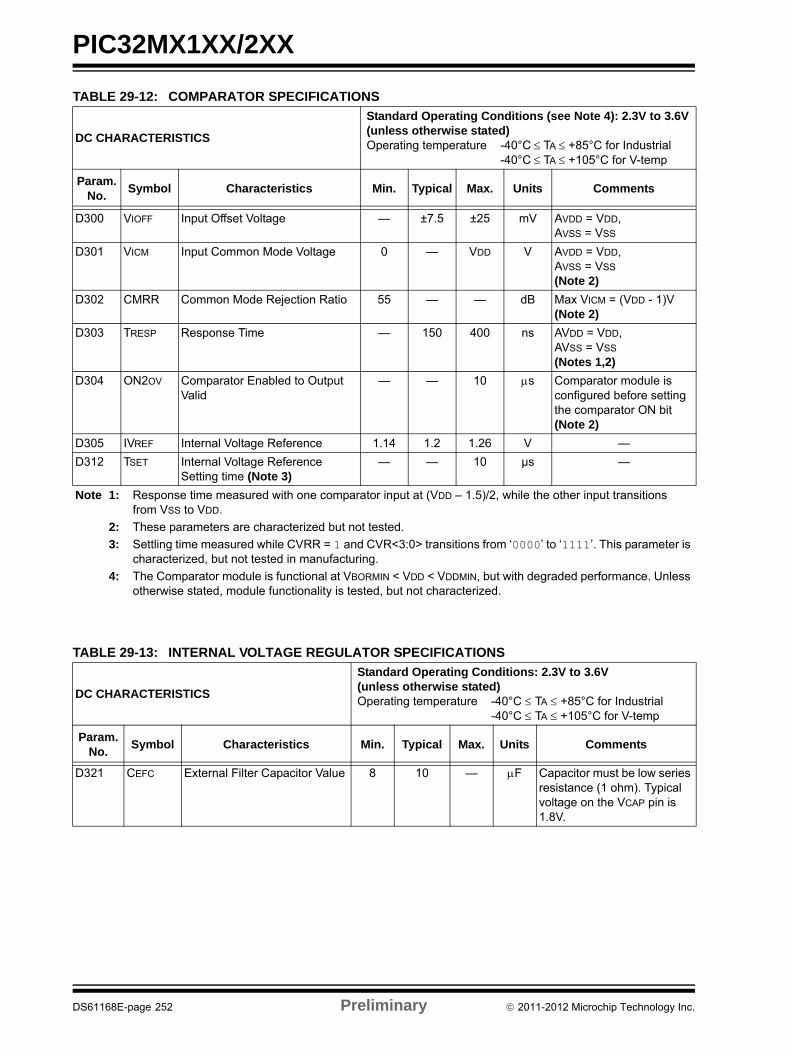
PIC32MX1XX/2XX
TABLE 29-12: COMPARATOR SPECIFICATIONS
DC CHARACTERISTICS
Standard Operating Conditions (see Note 4): 2.3V to 3.6V(unless otherwise stated)Operating temperature -40°C TA +85°C for Industrial
-40°C TA +105°C for V-temp
Param.No.
Symbol Characteristics Min. Typical Max. Units Comments
D300 VIOFF Input Offset Voltage — ±7.5 ±25 mV AVDD = VDD,AVSS = VSS
D301 VICM Input Common Mode Voltage 0 — VDD V AVDD = VDD,AVSS = VSS
(Note 2)
D302 CMRR Common Mode Rejection Ratio 55 — — dB Max VICM = (VDD - 1)V(Note 2)
D303 TRESP Response Time — 150 400 ns AVDD = VDD,AVSS = VSS
(Notes 1,2)
D304 ON2OV Comparator Enabled to Output Valid
— — 10 s Comparator module is configured before setting the comparator ON bit (Note 2)
D305 IVREF Internal Voltage Reference 1.14 1.2 1.26 V —
D312 TSET Internal Voltage Reference Setting time (Note 3)
— — 10 µs —
Note 1: Response time measured with one comparator input at (VDD – 1.5)/2, while the other input transitions from VSS to VDD.
2: These parameters are characterized but not tested.
3: Settling time measured while CVRR = 1 and CVR<3:0> transitions from ‘0000’ to ‘1111’. This parameter is characterized, but not tested in manufacturing.
4: The Comparator module is functional at VBORMIN < VDD < VDDMIN, but with degraded performance. Unless otherwise stated, module functionality is tested, but not characterized.
TABLE 29-13: INTERNAL VOLTAGE REGULATOR SPECIFICATIONS
DC CHARACTERISTICS
Standard Operating Conditions: 2.3V to 3.6V(unless otherwise stated)Operating temperature -40°C TA +85°C for Industrial
-40°C TA +105°C for V-temp
Param.No.
Symbol Characteristics Min. Typical Max. Units Comments
D321 CEFC External Filter Capacitor Value 8 10 — F Capacitor must be low series resistance (1 ohm). Typical voltage on the VCAP pin is 1.8V.
DS61168E-page 252 Preliminary 2011-2012 Microchip Technology Inc.
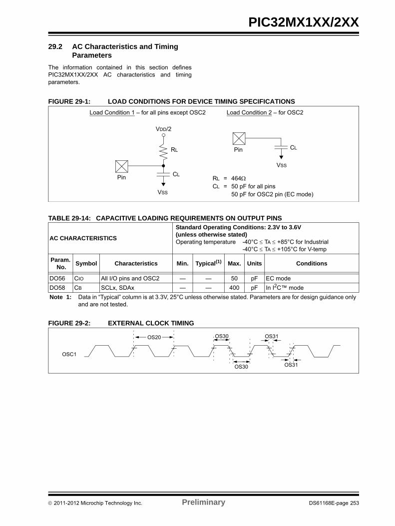
PIC32MX1XX/2XX
29.2 AC Characteristics and Timing Parameters
The information contained in this section definesPIC32MX1XX/2XX AC characteristics and timingparameters.
FIGURE 29-1: LOAD CONDITIONS FOR DEVICE TIMING SPECIFICATIONS
FIGURE 29-2: EXTERNAL CLOCK TIMING
VDD/2
CL
RL
Pin
Pin
VSS
VSS
CL
RL = 464CL = 50 pF for all pins
50 pF for OSC2 pin (EC mode)
Load Condition 1 – for all pins except OSC2 Load Condition 2 – for OSC2
TABLE 29-14: CAPACITIVE LOADING REQUIREMENTS ON OUTPUT PINS
AC CHARACTERISTICS
Standard Operating Conditions: 2.3V to 3.6V(unless otherwise stated)Operating temperature -40°C TA +85°C for Industrial
-40°C TA +105°C for V-temp
Param. No.
Symbol Characteristics Min. Typical(1) Max. Units Conditions
DO56 CIO All I/O pins and OSC2 — — 50 pF EC mode
DO58 CB SCLx, SDAx — — 400 pF In I2C™ mode
Note 1: Data in “Typical” column is at 3.3V, 25°C unless otherwise stated. Parameters are for design guidance only and are not tested.
OSC1
OS20 OS30
OS30
OS31
OS31
2011-2012 Microchip Technology Inc. Preliminary DS61168E-page 253
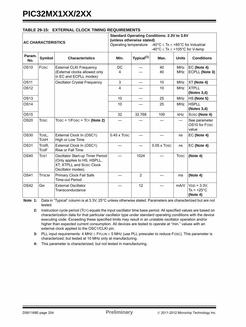
PIC32MX1XX/2XX
TABLE 29-15: EXTERNAL CLOCK TIMING REQUIREMENTS
AC CHARACTERISTICS
Standard Operating Conditions: 2.3V to 3.6V(unless otherwise stated)Operating temperature -40°C TA +85°C for Industrial
-40°C TA +105°C for V-temp
Param.No.
Symbol Characteristics Min. Typical(1) Max. Units Conditions
OS10 FOSC External CLKI Frequency(External clocks allowed onlyin EC and ECPLL modes)
DC4
——
4040
MHzMHz
EC (Note 4)ECPLL (Note 3)
OS11 Oscillator Crystal Frequency 3 — 10 MHz XT (Note 4)
OS12 4 — 10 MHz XTPLL(Notes 3,4)
OS13 10 — 25 MHz HS (Note 5)
OS14 10 — 25 MHz HSPLL(Notes 3,4)
OS15 32 32.768 100 kHz SOSC (Note 4)
OS20 TOSC TOSC = 1/FOSC = TCY (Note 2) — — — — See parameter OS10 for FOSC value
OS30 TOSL,TOSH
External Clock In (OSC1)High or Low Time
0.45 x TOSC — — ns EC (Note 4)
OS31 TOSR,TOSF
External Clock In (OSC1)Rise or Fall Time
— — 0.05 x TOSC ns EC (Note 4)
OS40 TOST Oscillator Start-up Timer Period(Only applies to HS, HSPLL, XT, XTPLL and SOSC Clock Oscillator modes)
— 1024 — TOSC (Note 4)
OS41 TFSCM Primary Clock Fail Safe Time-out Period
— 2 — ms (Note 4)
OS42 GM External Oscillator Transconductance
— 12 — mA/V VDD = 3.3V,TA = +25°C(Note 4)
Note 1: Data in “Typical” column is at 3.3V, 25°C unless otherwise stated. Parameters are characterized but are not tested.
2: Instruction cycle period (TCY) equals the input oscillator time base period. All specified values are based on characterization data for that particular oscillator type under standard operating conditions with the device executing code. Exceeding these specified limits may result in an unstable oscillator operation and/or higher than expected current consumption. All devices are tested to operate at “min.” values with an external clock applied to the OSC1/CLKI pin.
3: PLL input requirements: 4 MHZ FPLLIN 5 MHZ (use PLL prescaler to reduce FOSC). This parameter is characterized, but tested at 10 MHz only at manufacturing.
4: This parameter is characterized, but not tested in manufacturing.
DS61168E-page 254 Preliminary 2011-2012 Microchip Technology Inc.
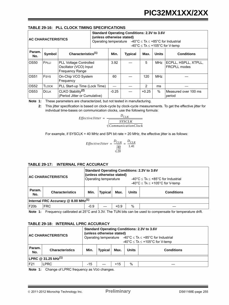
PIC32MX1XX/2XX
TABLE 29-16: PLL CLOCK TIMING SPECIFICATIONS
AC CHARACTERISTICS
Standard Operating Conditions: 2.3V to 3.6V(unless otherwise stated)Operating temperature -40°C TA +85°C for Industrial
-40°C TA +105°C for V-temp
Param.No.
Symbol Characteristics(1) Min. Typical Max. Units Conditions
OS50 FPLLI PLL Voltage Controlled Oscillator (VCO) Input Frequency Range
3.92 — 5 MHz ECPLL, HSPLL, XTPLL, FRCPLL modes
OS51 FSYS On-Chip VCO System Frequency
60 — 120 MHz —
OS52 TLOCK PLL Start-up Time (Lock Time) — — 2 ms —
OS53 DCLK CLKO Stability(2)
(Period Jitter or Cumulative)-0.25 — +0.25 % Measured over 100 ms
period
Note 1: These parameters are characterized, but not tested in manufacturing.
2: This jitter specification is based on clock-cycle by clock-cycle measurements. To get the effective jitter for individual time-bases on communication clocks, use the following formula:
For example, if SYSCLK = 40 MHz and SPI bit rate = 20 MHz, the effective jitter is as follows:
EffectiveJitterDCLK
SYSCLKCommunicationClock----------------------------------------------------------
--------------------------------------------------------------=
EffectiveJitterDCLK
4020------
--------------DCLK1.41
--------------= =
TABLE 29-17: INTERNAL FRC ACCURACY
AC CHARACTERISTICS
Standard Operating Conditions: 2.3V to 3.6V(unless otherwise stated)Operating temperature -40°C TA +85°C for Industrial
-40°C TA +105°C for V-temp
Param. No.
Characteristics Min. Typical Max. Units Conditions
Internal FRC Accuracy @ 8.00 MHz(1)
F20b FRC -0.9 — +0.9 % —
Note 1: Frequency calibrated at 25°C and 3.3V. The TUN bits can be used to compensate for temperature drift.
TABLE 29-18: INTERNAL LPRC ACCURACY
AC CHARACTERISTICS
Standard Operating Conditions: 2.3V to 3.6V(unless otherwise stated)Operating temperature -40°C TA +85°C for Industrial
-40°C TA +105°C for V-temp
Param.No.
Characteristics Min. Typical Max. Units Conditions
LPRC @ 31.25 kHz(1)
F21 LPRC -15 — +15 % —
Note 1: Change of LPRC frequency as VDD changes.
2011-2012 Microchip Technology Inc. Preliminary DS61168E-page 255
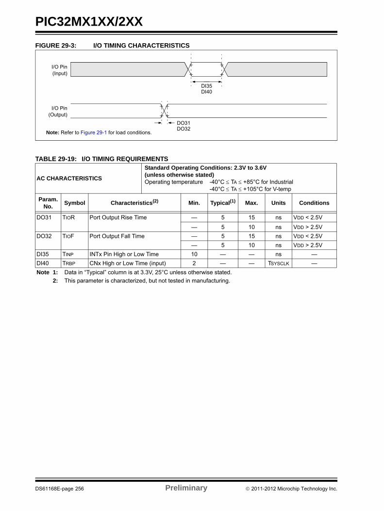
PIC32MX1XX/2XX
FIGURE 29-3: I/O TIMING CHARACTERISTICS
Note: Refer to Figure 29-1 for load conditions.
I/O Pin(Input)
I/O Pin(Output)
DI35DI40
DO31DO32
TABLE 29-19: I/O TIMING REQUIREMENTS
AC CHARACTERISTICS
Standard Operating Conditions: 2.3V to 3.6V(unless otherwise stated)Operating temperature -40°C TA +85°C for Industrial
-40°C TA +105°C for V-temp
Param.No.
Symbol Characteristics(2) Min. Typical(1) Max. Units Conditions
DO31 TIOR Port Output Rise Time — 5 15 ns VDD < 2.5V
— 5 10 ns VDD > 2.5V
DO32 TIOF Port Output Fall Time — 5 15 ns VDD < 2.5V
— 5 10 ns VDD > 2.5V
DI35 TINP INTx Pin High or Low Time 10 — — ns —
DI40 TRBP CNx High or Low Time (input) 2 — — TSYSCLK —
Note 1: Data in “Typical” column is at 3.3V, 25°C unless otherwise stated.
2: This parameter is characterized, but not tested in manufacturing.
DS61168E-page 256 Preliminary 2011-2012 Microchip Technology Inc.
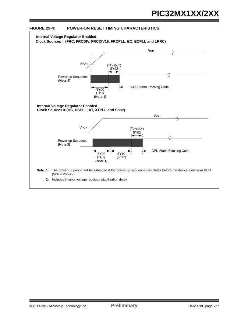
PIC32MX1XX/2XX
FIGURE 29-4: POWER-ON RESET TIMING CHARACTERISTICS
VDD
VPOR
Note 1: The power-up period will be extended if the power-up sequence completes before the device exits from BOR(VDD < VDDMIN).
2: Includes interval voltage regulator stabilization delay.
SY00
Power-up Sequence(Note 2)
Internal Voltage Regulator Enabled
(TPU)SY10
CPU Starts Fetching Code
Clock Sources = (HS, HSPLL, XT, XTPLL and SOSC)
VDD
VPOR
SY00
Power-up Sequence(Note 2)
Internal Voltage Regulator Enabled
(TPU)
(TSYSDLY)
CPU Starts Fetching Code
(Note 1)
(Note 1)
Clock Sources = (FRC, FRCDIV, FRCDIV16, FRCPLL, EC, ECPLL and LPRC)
(TOST)
SY02
(TSYSDLY)SY02
2011-2012 Microchip Technology Inc. Preliminary DS61168E-page 257
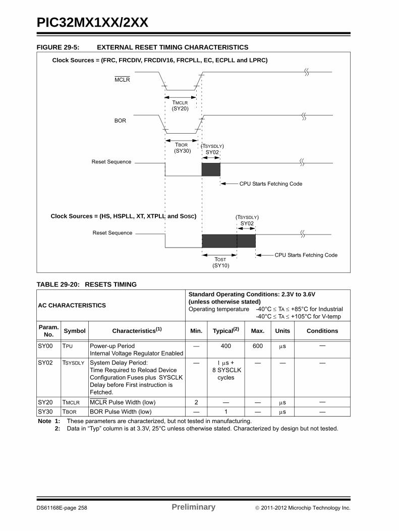
PIC32MX1XX/2XX
FIGURE 29-5: EXTERNAL RESET TIMING CHARACTERISTICS
TABLE 29-20: RESETS TIMING
AC CHARACTERISTICS
Standard Operating Conditions: 2.3V to 3.6V(unless otherwise stated)Operating temperature -40°C TA +85°C for Industrial
-40°C TA +105°C for V-temp
Param.No.
Symbol Characteristics(1) Min. Typical(2) Max. Units Conditions
SY00 TPU Power-up PeriodInternal Voltage Regulator Enabled
— 400 600 s —
SY02 TSYSDLY System Delay Period:Time Required to Reload Device Configuration Fuses plus SYSCLK Delay before First instruction is Fetched.
— s + 8 SYSCLK
cycles
— — —
SY20 TMCLR MCLR Pulse Width (low) 2 — — s —
SY30 TBOR BOR Pulse Width (low) — 1 — s —
Note 1: These parameters are characterized, but not tested in manufacturing.2: Data in “Typ” column is at 3.3V, 25°C unless otherwise stated. Characterized by design but not tested.
MCLR
(SY20)
Reset Sequence
(SY10)
CPU Starts Fetching Code
BOR
(SY30)
TOST
TMCLR
TBOR
Reset Sequence
CPU Starts Fetching Code
Clock Sources = (FRC, FRCDIV, FRCDIV16, FRCPLL, EC, ECPLL and LPRC)
Clock Sources = (HS, HSPLL, XT, XTPLL and SOSC) (TSYSDLY)SY02
(TSYSDLY)SY02
DS61168E-page 258 Preliminary 2011-2012 Microchip Technology Inc.
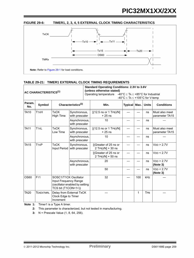
PIC32MX1XX/2XX
FIGURE 29-6: TIMER1, 2, 3, 4, 5 EXTERNAL CLOCK TIMING CHARACTERISTICS
Note: Refer to Figure 29-1 for load conditions.
Tx11
Tx15
Tx10
Tx20
TMRx
OS60
TxCK
TABLE 29-21: TIMER1 EXTERNAL CLOCK TIMING REQUIREMENTS
AC CHARACTERISTICS(1)
Standard Operating Conditions: 2.3V to 3.6V(unless otherwise stated)Operating temperature -40°C TA +85°C for Industrial
-40°C TA +105°C for V-temp
Param.No.
Symbol Characteristics(2) Min. Typical Max. Units Conditions
TA10 TTXH TxCKHigh Time
Synchronous,with prescaler
[(12.5 ns or 1 TPB)/N] + 25 ns
— — ns Must also meet parameter TA15
Asynchronous,with prescaler
10 — — ns —
TA11 TTXL TxCK Low Time
Synchronous,with prescaler
[(12.5 ns or 1 TPB)/N] + 25 ns
— — ns Must also meet parameter TA15
Asynchronous,with prescaler
10 — — ns —
TA15 TTXP TxCK Input Period
Synchronous,with prescaler
[(Greater of 25 ns or 2 TPB)/N] + 30 ns
— — ns VDD > 2.7V
[(Greater of 25 ns or 2 TPB)/N] + 50 ns
— — ns VDD < 2.7V
Asynchronous,with prescaler
20 — — ns VDD > 2.7V(Note 3)
50 — — ns VDD < 2.7V(Note 3)
OS60 FT1 SOSC1/T1CK Oscillator Input Frequency Range (oscillator enabled by setting TCS bit (T1CON<1>))
32 — 100 kHz —
TA20 TCKEXTMRL Delay from External TxCK Clock Edge to Timer Increment
— 1 TPB —
Note 1: Timer1 is a Type A timer.
2: This parameter is characterized, but not tested in manufacturing.
3: N = Prescale Value (1, 8, 64, 256).
2011-2012 Microchip Technology Inc. Preliminary DS61168E-page 259
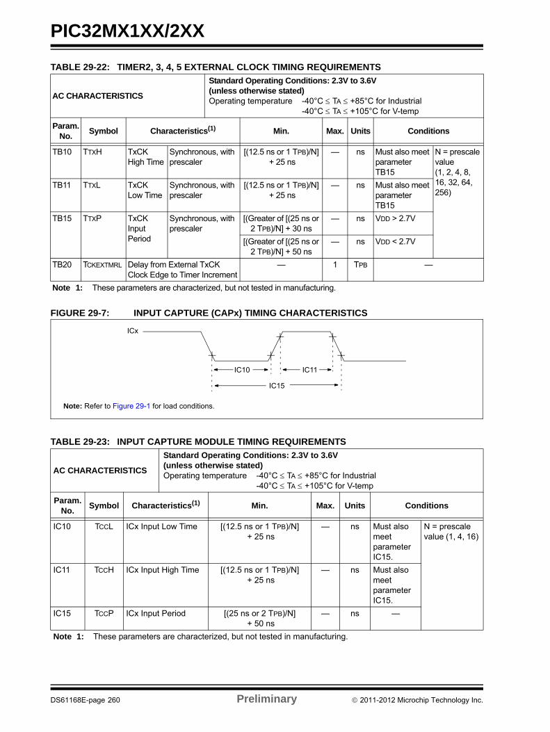
PIC32MX1XX/2XX
FIGURE 29-7: INPUT CAPTURE (CAPx) TIMING CHARACTERISTICS
TABLE 29-22: TIMER2, 3, 4, 5 EXTERNAL CLOCK TIMING REQUIREMENTS
AC CHARACTERISTICS
Standard Operating Conditions: 2.3V to 3.6V(unless otherwise stated)Operating temperature -40°C TA +85°C for Industrial
-40°C TA +105°C for V-temp
Param.No.
Symbol Characteristics(1) Min. Max. Units Conditions
TB10 TTXH TxCKHigh Time
Synchronous, with prescaler
[(12.5 ns or 1 TPB)/N] + 25 ns
— ns Must also meet parameter TB15
N = prescale value (1, 2, 4, 8, 16, 32, 64, 256)
TB11 TTXL TxCKLow Time
Synchronous, with prescaler
[(12.5 ns or 1 TPB)/N] + 25 ns
— ns Must also meet parameter TB15
TB15 TTXP TxCK Input Period
Synchronous, with prescaler
[(Greater of [(25 ns or 2 TPB)/N] + 30 ns
— ns VDD > 2.7V
[(Greater of [(25 ns or 2 TPB)/N] + 50 ns
— ns VDD < 2.7V
TB20 TCKEXTMRL Delay from External TxCK Clock Edge to Timer Increment
— 1 TPB —
Note 1: These parameters are characterized, but not tested in manufacturing.
ICx
IC10 IC11
IC15
Note: Refer to Figure 29-1 for load conditions.
TABLE 29-23: INPUT CAPTURE MODULE TIMING REQUIREMENTS
AC CHARACTERISTICS
Standard Operating Conditions: 2.3V to 3.6V(unless otherwise stated)Operating temperature -40°C TA +85°C for Industrial
-40°C TA +105°C for V-temp
Param.No.
Symbol Characteristics(1) Min. Max. Units Conditions
IC10 TCCL ICx Input Low Time [(12.5 ns or 1 TPB)/N] + 25 ns
— ns Must also meet parameter IC15.
N = prescale value (1, 4, 16)
IC11 TCCH ICx Input High Time [(12.5 ns or 1 TPB)/N] + 25 ns
— ns Must also meet parameter IC15.
IC15 TCCP ICx Input Period [(25 ns or 2 TPB)/N] + 50 ns
— ns —
Note 1: These parameters are characterized, but not tested in manufacturing.
DS61168E-page 260 Preliminary 2011-2012 Microchip Technology Inc.
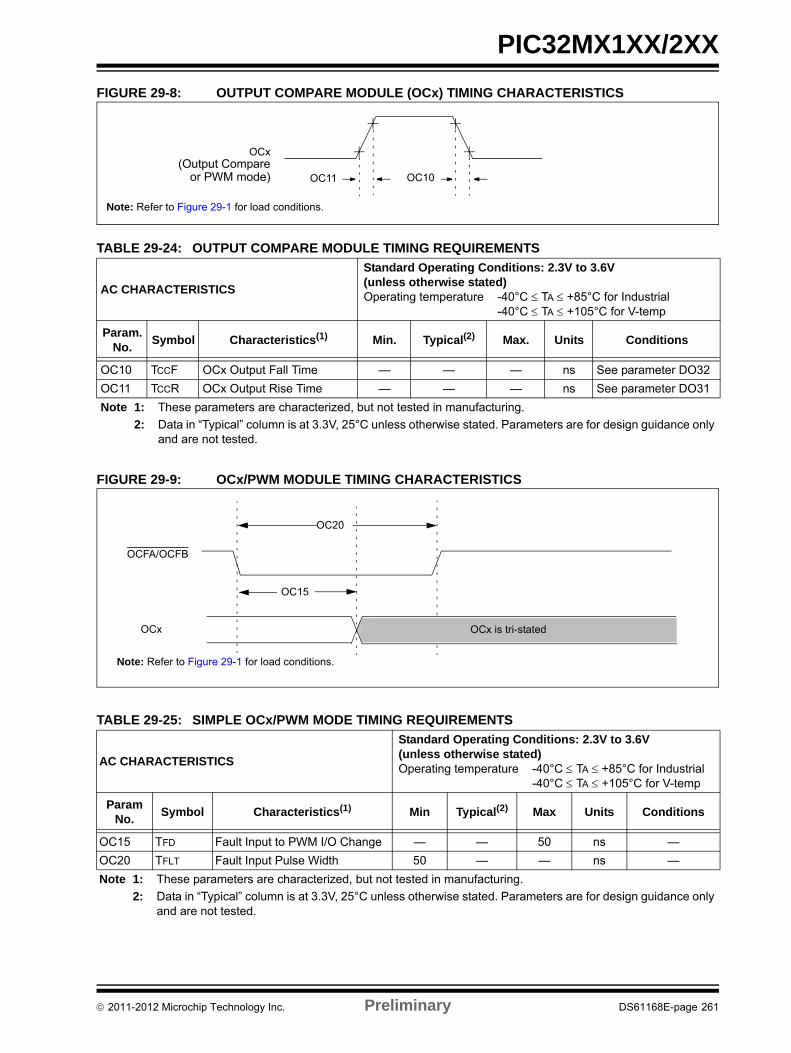
PIC32MX1XX/2XX
FIGURE 29-8: OUTPUT COMPARE MODULE (OCx) TIMING CHARACTERISTICS
TABLE 29-24: OUTPUT COMPARE MODULE TIMING REQUIREMENTS
FIGURE 29-9: OCx/PWM MODULE TIMING CHARACTERISTICS
AC CHARACTERISTICS
Standard Operating Conditions: 2.3V to 3.6V(unless otherwise stated)Operating temperature -40°C TA +85°C for Industrial
-40°C TA +105°C for V-temp
Param. No.
Symbol Characteristics(1) Min. Typical(2) Max. Units Conditions
OC10 TCCF OCx Output Fall Time — — — ns See parameter DO32
OC11 TCCR OCx Output Rise Time — — — ns See parameter DO31
Note 1: These parameters are characterized, but not tested in manufacturing.
2: Data in “Typical” column is at 3.3V, 25°C unless otherwise stated. Parameters are for design guidance only and are not tested.
OCx
OC11 OC10(Output Compare
Note: Refer to Figure 29-1 for load conditions.
or PWM mode)
OCFA/OCFB
OCx
OC20
OC15
Note: Refer to Figure 29-1 for load conditions.
OCx is tri-stated
TABLE 29-25: SIMPLE OCx/PWM MODE TIMING REQUIREMENTS
AC CHARACTERISTICS
Standard Operating Conditions: 2.3V to 3.6V(unless otherwise stated)Operating temperature -40°C TA +85°C for Industrial
-40°C TA +105°C for V-temp
Param No.
Symbol Characteristics(1) Min Typical(2) Max Units Conditions
OC15 TFD Fault Input to PWM I/O Change — — 50 ns —
OC20 TFLT Fault Input Pulse Width 50 — — ns —
Note 1: These parameters are characterized, but not tested in manufacturing.
2: Data in “Typical” column is at 3.3V, 25°C unless otherwise stated. Parameters are for design guidance only and are not tested.
2011-2012 Microchip Technology Inc. Preliminary DS61168E-page 261
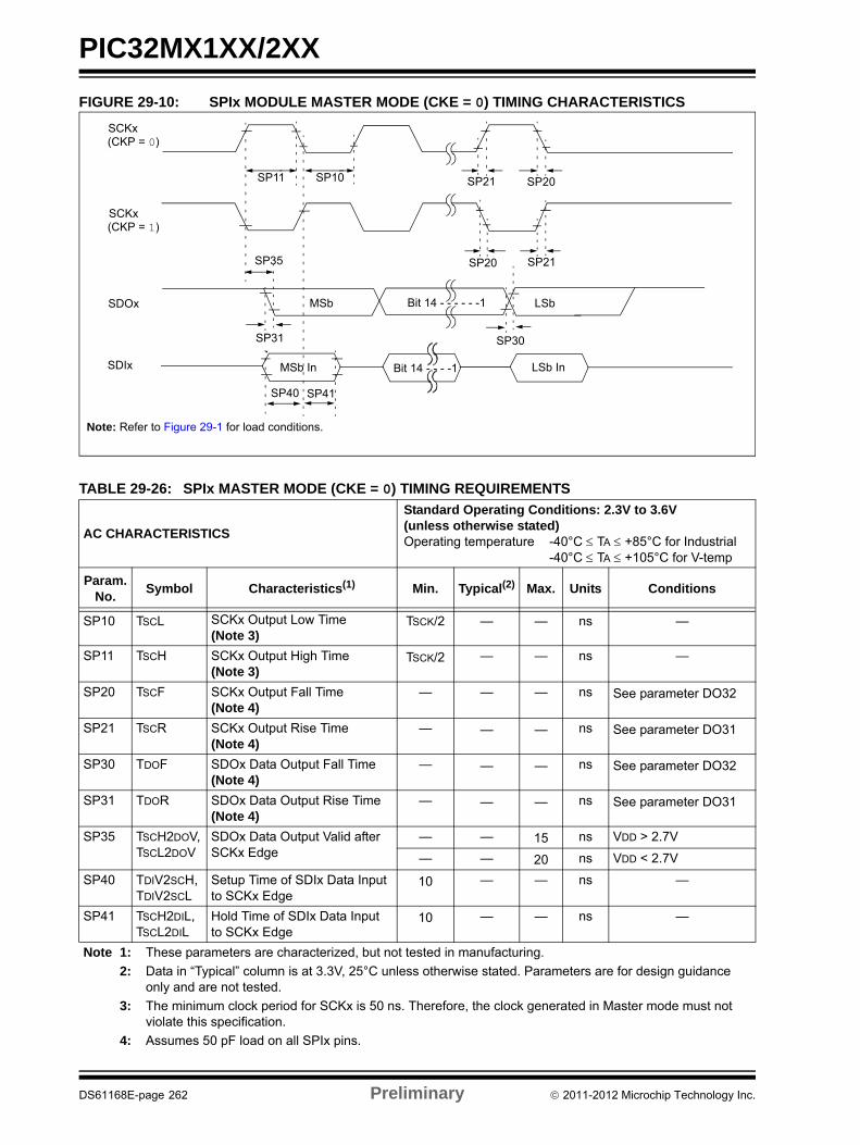
PIC32MX1XX/2XX
FIGURE 29-10: SPIx MODULE MASTER MODE (CKE = 0) TIMING CHARACTERISTICS
TABLE 29-26: SPIx MASTER MODE (CKE = 0) TIMING REQUIREMENTS
AC CHARACTERISTICS
Standard Operating Conditions: 2.3V to 3.6V(unless otherwise stated)Operating temperature -40°C TA +85°C for Industrial
-40°C TA +105°C for V-temp
Param.No.
Symbol Characteristics(1) Min. Typical(2) Max. Units Conditions
SP10 TSCL SCKx Output Low Time (Note 3)
TSCK/2 — — ns —
SP11 TSCH SCKx Output High Time (Note 3)
TSCK/2 — — ns —
SP20 TSCF SCKx Output Fall Time (Note 4)
— — — ns See parameter DO32
SP21 TSCR SCKx Output Rise Time (Note 4)
— — — ns See parameter DO31
SP30 TDOF SDOx Data Output Fall Time (Note 4)
— — — ns See parameter DO32
SP31 TDOR SDOx Data Output Rise Time (Note 4)
— — — ns See parameter DO31
SP35 TSCH2DOV,TSCL2DOV
SDOx Data Output Valid after SCKx Edge
— — 15 ns VDD > 2.7V
— — 20 ns VDD < 2.7V
SP40 TDIV2SCH,TDIV2SCL
Setup Time of SDIx Data Inputto SCKx Edge
10 — — ns —
SP41 TSCH2DIL,TSCL2DIL
Hold Time of SDIx Data Inputto SCKx Edge
10 — — ns —
Note 1: These parameters are characterized, but not tested in manufacturing.
2: Data in “Typical” column is at 3.3V, 25°C unless otherwise stated. Parameters are for design guidance only and are not tested.
3: The minimum clock period for SCKx is 50 ns. Therefore, the clock generated in Master mode must not violate this specification.
4: Assumes 50 pF load on all SPIx pins.
SCKx(CKP = 0)
SCKx(CKP = 1)
SDOx
SDIx
SP11 SP10
SP40 SP41
SP21SP20SP35
SP20SP21
MSb LSbBit 14 - - - - - -1
MSb In LSb InBit 14 - - - -1
SP30SP31
Note: Refer to Figure 29-1 for load conditions.
DS61168E-page 262 Preliminary 2011-2012 Microchip Technology Inc.
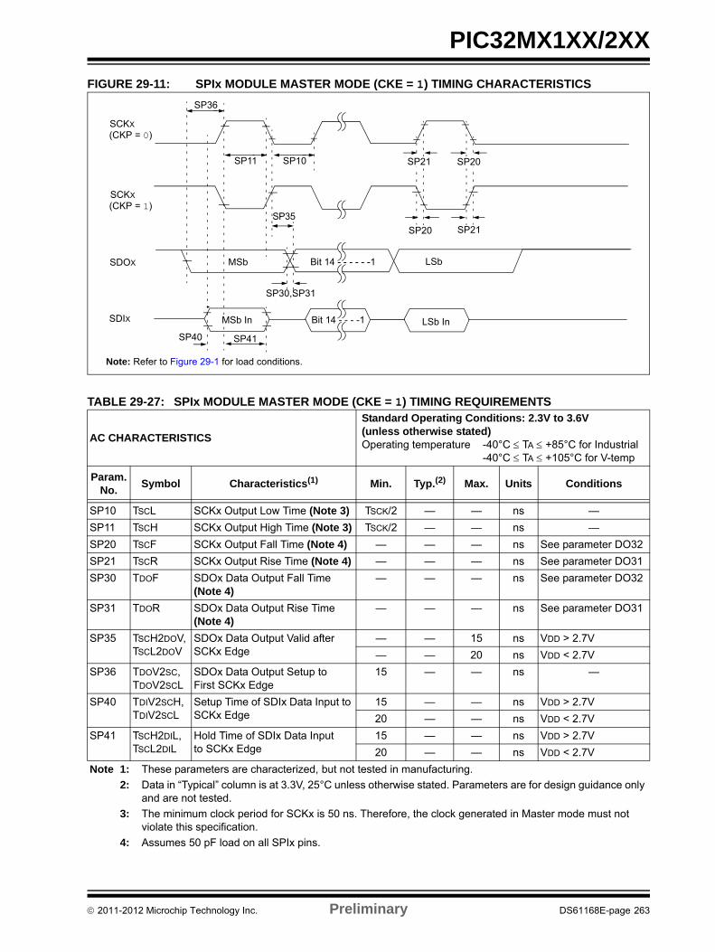
PIC32MX1XX/2XX
FIGURE 29-11: SPIx MODULE MASTER MODE (CKE = 1) TIMING CHARACTERISTICS
TABLE 29-27: SPIx MODULE MASTER MODE (CKE = 1) TIMING REQUIREMENTS
AC CHARACTERISTICS
Standard Operating Conditions: 2.3V to 3.6V(unless otherwise stated)Operating temperature -40°C TA +85°C for Industrial
-40°C TA +105°C for V-temp
Param.No.
Symbol Characteristics(1) Min. Typ.(2) Max. Units Conditions
SP10 TSCL SCKx Output Low Time (Note 3) TSCK/2 — — ns —
SP11 TSCH SCKx Output High Time (Note 3) TSCK/2 — — ns —
SP20 TSCF SCKx Output Fall Time (Note 4) — — — ns See parameter DO32
SP21 TSCR SCKx Output Rise Time (Note 4) — — — ns See parameter DO31
SP30 TDOF SDOx Data Output Fall Time (Note 4)
— — — ns See parameter DO32
SP31 TDOR SDOx Data Output Rise Time (Note 4)
— — — ns See parameter DO31
SP35 TSCH2DOV,TSCL2DOV
SDOx Data Output Valid afterSCKx Edge
— — 15 ns VDD > 2.7V
— — 20 ns VDD < 2.7V
SP36 TDOV2SC, TDOV2SCL
SDOx Data Output Setup toFirst SCKx Edge
15 — — ns —
SP40 TDIV2SCH, TDIV2SCL
Setup Time of SDIx Data Input to SCKx Edge
15 — — ns VDD > 2.7V
20 — — ns VDD < 2.7V
SP41 TSCH2DIL, TSCL2DIL
Hold Time of SDIx Data Inputto SCKx Edge
15 — — ns VDD > 2.7V
20 — — ns VDD < 2.7V
Note 1: These parameters are characterized, but not tested in manufacturing.
2: Data in “Typical” column is at 3.3V, 25°C unless otherwise stated. Parameters are for design guidance only and are not tested.
3: The minimum clock period for SCKx is 50 ns. Therefore, the clock generated in Master mode must not violate this specification.
4: Assumes 50 pF load on all SPIx pins.
SCKX
(CKP = 0)
SCKX
(CKP = 1)
SDOX
SDIX
SP36
SP30,SP31
SP35
MSb Bit 14 - - - - - -1
LSb InBit 14 - - - -1
LSb
Note: Refer to Figure 29-1 for load conditions.
SP11 SP10
SP21SP20
SP40 SP41
SP20SP21
MSb In
2011-2012 Microchip Technology Inc. Preliminary DS61168E-page 263
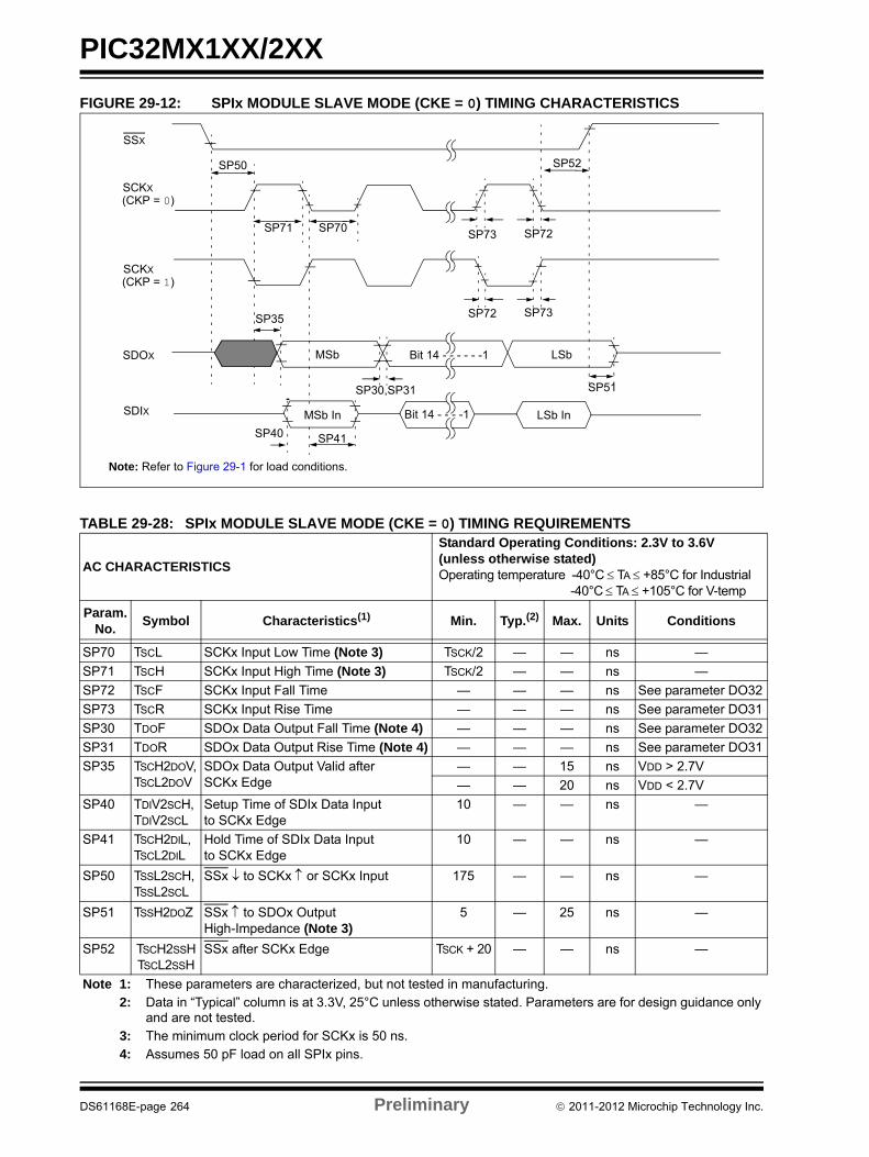
PIC32MX1XX/2XX
FIGURE 29-12: SPIx MODULE SLAVE MODE (CKE = 0) TIMING CHARACTERISTICS
SSX
SCKX(CKP = 0)
SCKX(CKP = 1)
SDOX
SP50
SP40 SP41
SP30,SP31 SP51
SP35
MSb LSbBit 14 - - - - - -1
Bit 14 - - - -1 LSb In
SP52
SP73SP72
SP72SP73SP71 SP70
Note: Refer to Figure 29-1 for load conditions.
SDIX MSb In
TABLE 29-28: SPIx MODULE SLAVE MODE (CKE = 0) TIMING REQUIREMENTS
AC CHARACTERISTICS
Standard Operating Conditions: 2.3V to 3.6V(unless otherwise stated)Operating temperature -40°C TA +85°C for Industrial
-40°C TA +105°C for V-temp
Param.No.
Symbol Characteristics(1) Min. Typ.(2) Max. Units Conditions
SP70 TSCL SCKx Input Low Time (Note 3) TSCK/2 — — ns —
SP71 TSCH SCKx Input High Time (Note 3) TSCK/2 — — ns —
SP72 TSCF SCKx Input Fall Time — — — ns See parameter DO32
SP73 TSCR SCKx Input Rise Time — — — ns See parameter DO31
SP30 TDOF SDOx Data Output Fall Time (Note 4) — — — ns See parameter DO32
SP31 TDOR SDOx Data Output Rise Time (Note 4) — — — ns See parameter DO31
SP35 TSCH2DOV,TSCL2DOV
SDOx Data Output Valid afterSCKx Edge
— — 15 ns VDD > 2.7V
— — 20 ns VDD < 2.7V
SP40 TDIV2SCH, TDIV2SCL
Setup Time of SDIx Data Inputto SCKx Edge
10 — — ns —
SP41 TSCH2DIL, TSCL2DIL
Hold Time of SDIx Data Inputto SCKx Edge
10 — — ns —
SP50 TSSL2SCH, TSSL2SCL
SSx to SCKx or SCKx Input 175 — — ns —
SP51 TSSH2DOZ SSx to SDOx Output High-Impedance (Note 3)
5 — 25 ns —
SP52 TSCH2SSHTSCL2SSH
SSx after SCKx Edge TSCK + 20 — — ns —
Note 1: These parameters are characterized, but not tested in manufacturing.2: Data in “Typical” column is at 3.3V, 25°C unless otherwise stated. Parameters are for design guidance only
and are not tested.3: The minimum clock period for SCKx is 50 ns.4: Assumes 50 pF load on all SPIx pins.
DS61168E-page 264 Preliminary 2011-2012 Microchip Technology Inc.
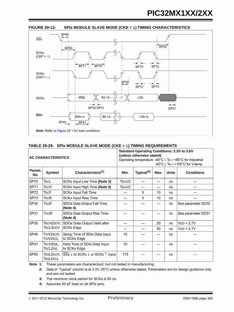
PIC32MX1XX/2XX
FIGURE 29-13: SPIx MODULE SLAVE MODE (CKE = 1) TIMING CHARACTERISTICS
SSx
SCKx(CKP = 0)
SCKx(CKP = 1)
SDOx
SDI
SP60
SDIx
SP30,SP31
MSb Bit 14 - - - - - -1 LSb
SP51
MSb In Bit 14 - - - -1 LSb In
SP52
SP73SP72
SP72SP73SP71
SP40 SP41
Note: Refer to Figure 29-1 for load conditions.
SP50
SP70
SP35
TABLE 29-29: SPIx MODULE SLAVE MODE (CKE = 1) TIMING REQUIREMENTS
AC CHARACTERISTICS
Standard Operating Conditions: 2.3V to 3.6V(unless otherwise stated)Operating temperature -40°C TA +85°C for Industrial
-40°C TA +105°C for V-temp
Param.No.
Symbol Characteristics(1) Min. Typical(2) Max. Units Conditions
SP70 TSCL SCKx Input Low Time (Note 3) TSCK/2 — — ns —
SP71 TSCH SCKx Input High Time (Note 3) TSCK/2 — — ns —
SP72 TSCF SCKx Input Fall Time — 5 10 ns —
SP73 TSCR SCKx Input Rise Time — 5 10 ns —
SP30 TDOF SDOx Data Output Fall Time (Note 4)
— — — ns See parameter DO32
SP31 TDOR SDOx Data Output Rise Time (Note 4)
— — — ns See parameter DO31
SP35 TSCH2DOV,TSCL2DOV
SDOx Data Output Valid afterSCKx Edge
— — 20 ns VDD > 2.7V
— — 30 ns VDD < 2.7V
SP40 TDIV2SCH, TDIV2SCL
Setup Time of SDIx Data Inputto SCKx Edge
10 — — ns —
SP41 TSCH2DIL, TSCL2DIL
Hold Time of SDIx Data Inputto SCKx Edge
10 — — ns —
SP50 TSSL2SCH, TSSL2SCL
SSx to SCKx or SCKx Input 175 — — ns —
Note 1: These parameters are characterized, but not tested in manufacturing.
2: Data in “Typical” column is at 3.3V, 25°C unless otherwise stated. Parameters are for design guidance only and are not tested.
3: The minimum clock period for SCKx is 50 ns.
4: Assumes 50 pF load on all SPIx pins.
2011-2012 Microchip Technology Inc. Preliminary DS61168E-page 265
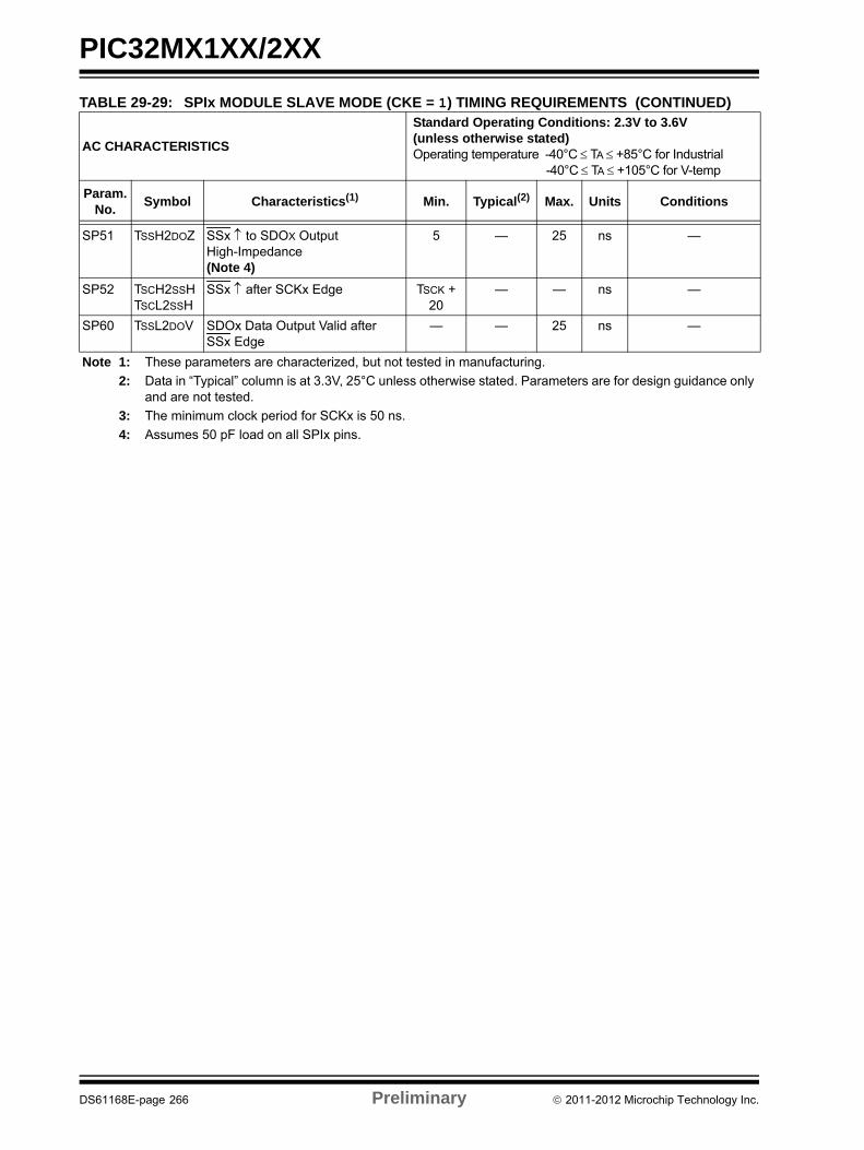
PIC32MX1XX/2XX
SP51 TSSH2DOZ SSx to SDOX OutputHigh-Impedance (Note 4)
5 — 25 ns —
SP52 TSCH2SSHTSCL2SSH
SSx after SCKx Edge TSCK + 20
— — ns —
SP60 TSSL2DOV SDOx Data Output Valid afterSSx Edge
— — 25 ns —
TABLE 29-29: SPIx MODULE SLAVE MODE (CKE = 1) TIMING REQUIREMENTS (CONTINUED)
AC CHARACTERISTICS
Standard Operating Conditions: 2.3V to 3.6V(unless otherwise stated)Operating temperature -40°C TA +85°C for Industrial
-40°C TA +105°C for V-temp
Param.No.
Symbol Characteristics(1) Min. Typical(2) Max. Units Conditions
Note 1: These parameters are characterized, but not tested in manufacturing.
2: Data in “Typical” column is at 3.3V, 25°C unless otherwise stated. Parameters are for design guidance only and are not tested.
3: The minimum clock period for SCKx is 50 ns.
4: Assumes 50 pF load on all SPIx pins.
DS61168E-page 266 Preliminary 2011-2012 Microchip Technology Inc.
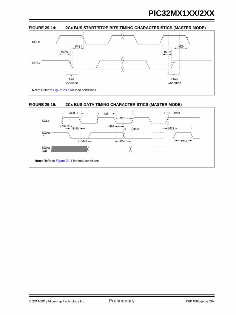
PIC32MX1XX/2XX
FIGURE 29-14: I2Cx BUS START/STOP BITS TIMING CHARACTERISTICS (MASTER MODE)
FIGURE 29-15: I2Cx BUS DATA TIMING CHARACTERISTICS (MASTER MODE)
SCLx
SDAx
StartCondition
StopCondition
Note: Refer to Figure 29-1 for load conditions.
IM30
IM31 IM34
IM33
IM11IM10 IM33
IM11
IM10
IM20
IM26IM25
IM40 IM40 IM45
IM21
SCLx
SDAxIn
SDAxOut
Note: Refer to Figure 29-1 for load conditions.
2011-2012 Microchip Technology Inc. Preliminary DS61168E-page 267
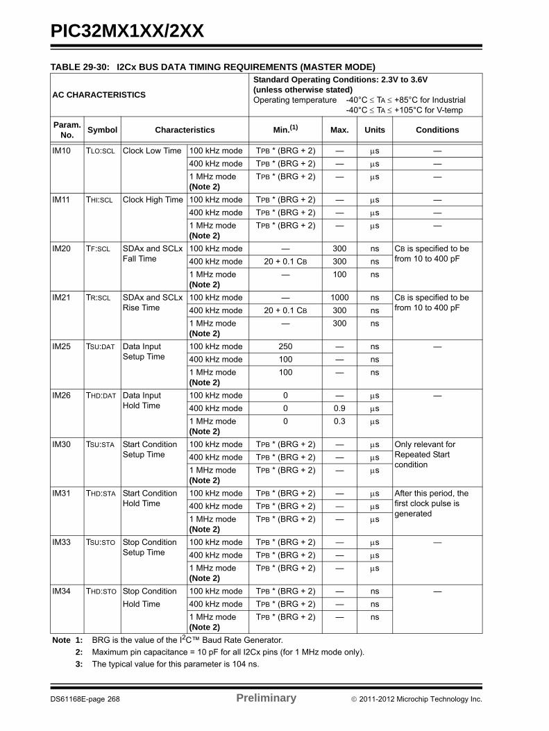
PIC32MX1XX/2XX
TABLE 29-30: I2Cx BUS DATA TIMING REQUIREMENTS (MASTER MODE)
AC CHARACTERISTICS
Standard Operating Conditions: 2.3V to 3.6V(unless otherwise stated)Operating temperature -40°C TA +85°C for Industrial
-40°C TA +105°C for V-temp
Param.No.
Symbol Characteristics Min.(1) Max. Units Conditions
IM10 TLO:SCL Clock Low Time 100 kHz mode TPB * (BRG + 2) — s —
400 kHz mode TPB * (BRG + 2) — s —
1 MHz mode (Note 2)
TPB * (BRG + 2) — s —
IM11 THI:SCL Clock High Time 100 kHz mode TPB * (BRG + 2) — s —
400 kHz mode TPB * (BRG + 2) — s —
1 MHz mode (Note 2)
TPB * (BRG + 2) — s —
IM20 TF:SCL SDAx and SCLxFall Time
100 kHz mode — 300 ns CB is specified to be from 10 to 400 pF400 kHz mode 20 + 0.1 CB 300 ns
1 MHz mode (Note 2)
— 100 ns
IM21 TR:SCL SDAx and SCLxRise Time
100 kHz mode — 1000 ns CB is specified to be from 10 to 400 pF400 kHz mode 20 + 0.1 CB 300 ns
1 MHz mode (Note 2)
— 300 ns
IM25 TSU:DAT Data InputSetup Time
100 kHz mode 250 — ns —
400 kHz mode 100 — ns
1 MHz mode (Note 2)
100 — ns
IM26 THD:DAT Data InputHold Time
100 kHz mode 0 — s —
400 kHz mode 0 0.9 s
1 MHz mode (Note 2)
0 0.3 s
IM30 TSU:STA Start ConditionSetup Time
100 kHz mode TPB * (BRG + 2) — s Only relevant for Repeated Startcondition
400 kHz mode TPB * (BRG + 2) — s
1 MHz mode (Note 2)
TPB * (BRG + 2) — s
IM31 THD:STA Start Condition Hold Time
100 kHz mode TPB * (BRG + 2) — s After this period, thefirst clock pulse isgenerated
400 kHz mode TPB * (BRG + 2) — s
1 MHz mode (Note 2)
TPB * (BRG + 2) — s
IM33 TSU:STO Stop Condition Setup Time
100 kHz mode TPB * (BRG + 2) — s —
400 kHz mode TPB * (BRG + 2) — s
1 MHz mode (Note 2)
TPB * (BRG + 2) — s
IM34 THD:STO Stop Condition 100 kHz mode TPB * (BRG + 2) — ns —
Hold Time 400 kHz mode TPB * (BRG + 2) — ns
1 MHz mode (Note 2)
TPB * (BRG + 2) — ns
Note 1: BRG is the value of the I2C™ Baud Rate Generator.
2: Maximum pin capacitance = 10 pF for all I2Cx pins (for 1 MHz mode only).
3: The typical value for this parameter is 104 ns.
DS61168E-page 268 Preliminary 2011-2012 Microchip Technology Inc.
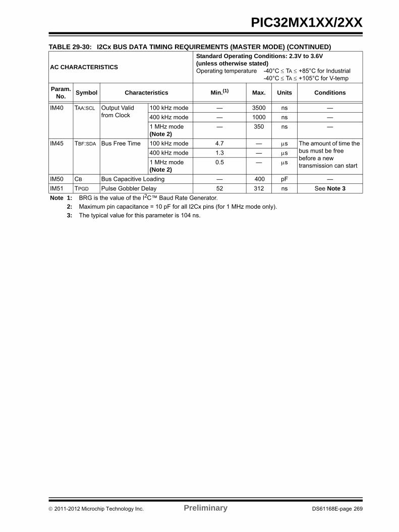
PIC32MX1XX/2XX
IM40 TAA:SCL Output Valid from Clock
100 kHz mode — 3500 ns —
400 kHz mode — 1000 ns —
1 MHz mode (Note 2)
— 350 ns —
IM45 TBF:SDA Bus Free Time 100 kHz mode 4.7 — s The amount of time the bus must be free before a newtransmission can start
400 kHz mode 1.3 — s
1 MHz mode (Note 2)
0.5 — s
IM50 CB Bus Capacitive Loading — 400 pF —
IM51 TPGD Pulse Gobbler Delay 52 312 ns See Note 3
TABLE 29-30: I2Cx BUS DATA TIMING REQUIREMENTS (MASTER MODE) (CONTINUED)
AC CHARACTERISTICS
Standard Operating Conditions: 2.3V to 3.6V(unless otherwise stated)Operating temperature -40°C TA +85°C for Industrial
-40°C TA +105°C for V-temp
Param.No.
Symbol Characteristics Min.(1) Max. Units Conditions
Note 1: BRG is the value of the I2C™ Baud Rate Generator.
2: Maximum pin capacitance = 10 pF for all I2Cx pins (for 1 MHz mode only).
3: The typical value for this parameter is 104 ns.
2011-2012 Microchip Technology Inc. Preliminary DS61168E-page 269
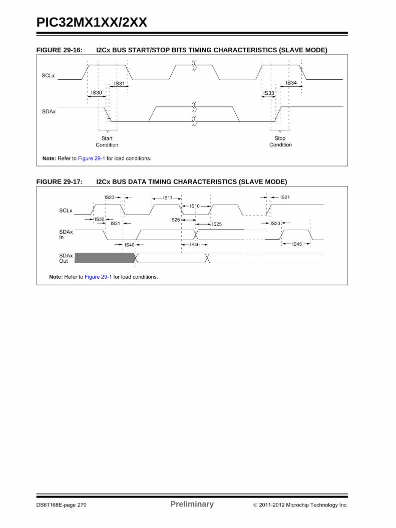
PIC32MX1XX/2XX
FIGURE 29-16: I2Cx BUS START/STOP BITS TIMING CHARACTERISTICS (SLAVE MODE)
FIGURE 29-17: I2Cx BUS DATA TIMING CHARACTERISTICS (SLAVE MODE)
IS34SCLx
SDAx
StartCondition
StopCondition
IS33
Note: Refer to Figure 29-1 for load conditions.
IS31
IS30
IS30IS31 IS33
IS11
IS10
IS20
IS26IS25
IS40 IS40 IS45
IS21
SCLx
SDAxIn
SDAxOut
Note: Refer to Figure 29-1 for load conditions.
DS61168E-page 270 Preliminary 2011-2012 Microchip Technology Inc.
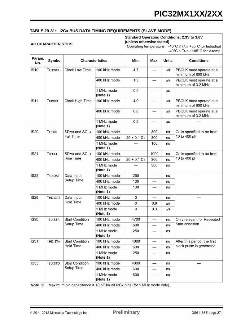
PIC32MX1XX/2XX
TABLE 29-31: I2Cx BUS DATA TIMING REQUIREMENTS (SLAVE MODE)
AC CHARACTERISTICS
Standard Operating Conditions: 2.3V to 3.6V(unless otherwise stated)Operating temperature -40°C TA +85°C for Industrial
-40°C TA +105°C for V-temp
Param. No.
Symbol Characteristics Min. Max. Units Conditions
IS10 TLO:SCL Clock Low Time 100 kHz mode 4.7 — s PBCLK must operate at a minimum of 800 kHz
400 kHz mode 1.3 — s PBCLK must operate at a minimum of 3.2 MHz
1 MHz mode (Note 1)
0.5 — s —
IS11 THI:SCL Clock High Time 100 kHz mode 4.0 — s PBCLK must operate at a minimum of 800 kHz
400 kHz mode 0.6 — s PBCLK must operate at a minimum of 3.2 MHz
1 MHz mode (Note 1)
0.5 — s —
IS20 TF:SCL SDAx and SCLxFall Time
100 kHz mode — 300 ns CB is specified to be from10 to 400 pF400 kHz mode 20 + 0.1 CB 300 ns
1 MHz mode (Note 1)
— 100 ns
IS21 TR:SCL SDAx and SCLxRise Time
100 kHz mode — 1000 ns CB is specified to be from10 to 400 pF400 kHz mode 20 + 0.1 CB 300 ns
1 MHz mode (Note 1)
— 300 ns
IS25 TSU:DAT Data InputSetup Time
100 kHz mode 250 — ns —
400 kHz mode 100 — ns
1 MHz mode (Note 1)
100 — ns
IS26 THD:DAT Data InputHold Time
100 kHz mode 0 — ns —
400 kHz mode 0 0.9 s
1 MHz mode (Note 1)
0 0.3 s
IS30 TSU:STA Start ConditionSetup Time
100 kHz mode 4700 — ns Only relevant for Repeated Start condition400 kHz mode 600 — ns
1 MHz mode (Note 1)
250 — ns
IS31 THD:STA Start Condition Hold Time
100 kHz mode 4000 — ns After this period, the first clock pulse is generated400 kHz mode 600 — ns
1 MHz mode (Note 1)
250 — ns
IS33 TSU:STO Stop Condition Setup Time
100 kHz mode 4000 — ns —
400 kHz mode 600 — ns
1 MHz mode (Note 1)
600 — ns
Note 1: Maximum pin capacitance = 10 pF for all I2Cx pins (for 1 MHz mode only).
2011-2012 Microchip Technology Inc. Preliminary DS61168E-page 271
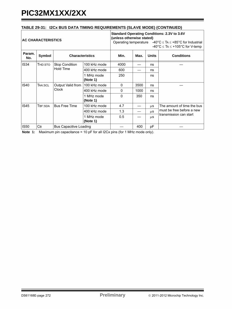
PIC32MX1XX/2XX
IS34 THD:STO Stop ConditionHold Time
100 kHz mode 4000 — ns —
400 kHz mode 600 — ns
1 MHz mode (Note 1)
250 ns
IS40 TAA:SCL Output Valid from Clock
100 kHz mode 0 3500 ns —
400 kHz mode 0 1000 ns
1 MHz mode (Note 1)
0 350 ns
IS45 TBF:SDA Bus Free Time 100 kHz mode 4.7 — s The amount of time the bus must be free before a new transmission can start
400 kHz mode 1.3 — s
1 MHz mode (Note 1)
0.5 — s
IS50 CB Bus Capacitive Loading — 400 pF —
TABLE 29-31: I2Cx BUS DATA TIMING REQUIREMENTS (SLAVE MODE) (CONTINUED)
AC CHARACTERISTICS
Standard Operating Conditions: 2.3V to 3.6V(unless otherwise stated)Operating temperature -40°C TA +85°C for Industrial
-40°C TA +105°C for V-temp
Param. No.
Symbol Characteristics Min. Max. Units Conditions
Note 1: Maximum pin capacitance = 10 pF for all I2Cx pins (for 1 MHz mode only).
DS61168E-page 272 Preliminary 2011-2012 Microchip Technology Inc.
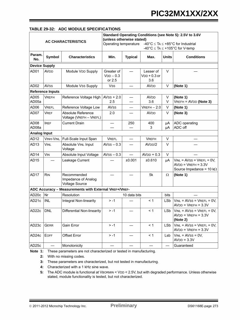
PIC32MX1XX/2XX
TABLE 29-32: ADC MODULE SPECIFICATIONS
AC CHARACTERISTICS
Standard Operating Conditions (see Note 5): 2.5V to 3.6V(unless otherwise stated)Operating temperature -40°C TA +85°C for Industrial
-40°C TA +105°C for V-temp
Param. No.
Symbol Characteristics Min. Typical Max. Units Conditions
Device Supply
AD01 AVDD Module VDD Supply Greater of VDD – 0.3
or 2.5
— Lesser of VDD + 0.3 or
3.6
V —
AD02 AVSS Module VSS Supply VSS — AVDD V (Note 1)
Reference Inputs
AD05AD05a
VREFH Reference Voltage High AVSS + 2.02.5
——
AVDD
3.6VV
(Note 1)VREFH = AVDD (Note 3)
AD06 VREFL Reference Voltage Low AVSS — VREFH – 2.0 V (Note 1)
AD07 VREF Absolute Reference Voltage (VREFH – VREFL)
2.0 — AVDD V (Note 3)
AD08AD08a
IREF Current Drain ——
250—
4003
µAµA
ADC operatingADC off
Analog Input
AD12 VINH-VINL Full-Scale Input Span VREFL — VREFH V —
AD13 VINL Absolute VINL Input Voltage
AVSS – 0.3 — AVDD/2 V —
AD14 VIN Absolute Input Voltage AVSS – 0.3 — AVDD + 0.3 V —
AD15 — Leakage Current — ±0.001 ±0.610 µA VINL = AVSS = VREFL = 0V,AVDD = VREFH = 3.3VSource Impedance = 10 k
AD17 RIN Recommended Impedance of Analog Voltage Source
— — 5k (Note 1)
ADC Accuracy – Measurements with External VREF+/VREF-
AD20c Nr Resolution 10 data bits bits —
AD21c INL Integral Non-linearity > -1 — < 1 LSb VINL = AVSS = VREFL = 0V, AVDD = VREFH = 3.3V
AD22c DNL Differential Non-linearity > -1 — < 1 LSb VINL = AVSS = VREFL = 0V, AVDD = VREFH = 3.3V (Note 2)
AD23c GERR Gain Error > -1 — < 1 LSb VINL = AVSS = VREFL = 0V, AVDD = VREFH = 3.3V
AD24c EOFF Offset Error > -1 — < 1 Lsb VINL = AVSS = 0V, AVDD = 3.3V
AD25c — Monotonicity — — — — Guaranteed
Note 1: These parameters are not characterized or tested in manufacturing.
2: With no missing codes.
3: These parameters are characterized, but not tested in manufacturing.
4: Characterized with a 1 kHz sine wave.
5: The ADC module is functional at VBORMIN < VDD < 2.5V, but with degraded performance. Unless otherwise stated, module functionality is tested, but not characterized.
2011-2012 Microchip Technology Inc. Preliminary DS61168E-page 273
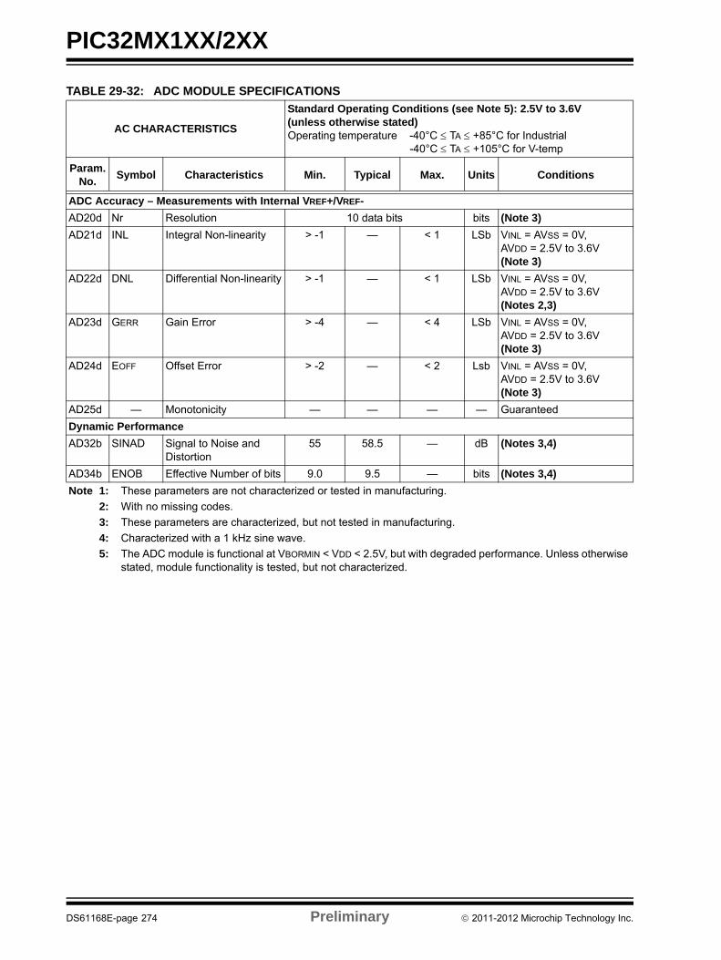
PIC32MX1XX/2XX
ADC Accuracy – Measurements with Internal VREF+/VREF-
AD20d Nr Resolution 10 data bits bits (Note 3)
AD21d INL Integral Non-linearity > -1 — < 1 LSb VINL = AVSS = 0V, AVDD = 2.5V to 3.6V (Note 3)
AD22d DNL Differential Non-linearity > -1 — < 1 LSb VINL = AVSS = 0V, AVDD = 2.5V to 3.6V (Notes 2,3)
AD23d GERR Gain Error > -4 — < 4 LSb VINL = AVSS = 0V, AVDD = 2.5V to 3.6V(Note 3)
AD24d EOFF Offset Error > -2 — < 2 Lsb VINL = AVSS = 0V, AVDD = 2.5V to 3.6V(Note 3)
AD25d — Monotonicity — — — — Guaranteed
Dynamic Performance
AD32b SINAD Signal to Noise and Distortion
55 58.5 — dB (Notes 3,4)
AD34b ENOB Effective Number of bits 9.0 9.5 — bits (Notes 3,4)
TABLE 29-32: ADC MODULE SPECIFICATIONS
AC CHARACTERISTICS
Standard Operating Conditions (see Note 5): 2.5V to 3.6V(unless otherwise stated)Operating temperature -40°C TA +85°C for Industrial
-40°C TA +105°C for V-temp
Param. No.
Symbol Characteristics Min. Typical Max. Units Conditions
Note 1: These parameters are not characterized or tested in manufacturing.
2: With no missing codes.
3: These parameters are characterized, but not tested in manufacturing.
4: Characterized with a 1 kHz sine wave.
5: The ADC module is functional at VBORMIN < VDD < 2.5V, but with degraded performance. Unless otherwise stated, module functionality is tested, but not characterized.
DS61168E-page 274 Preliminary 2011-2012 Microchip Technology Inc.
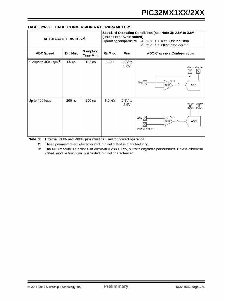
PIC32MX1XX/2XX
TABLE 29-33: 10-BIT CONVERSION RATE PARAMETERS
AC CHARACTERISTICS(2)
Standard Operating Conditions (see Note 3): 2.5V to 3.6V(unless otherwise stated)Operating temperature -40°C TA +85°C for Industrial
-40°C TA +105°C for V-temp
ADC Speed TAD Min.Sampling Time Min.
RS Max. VDD ADC Channels Configuration
1 Msps to 400 ksps(1) 65 ns 132 ns 500 3.0V to 3.6V
Up to 400 ksps 200 ns 200 ns 5.0 k 2.5V to 3.6V
Note 1: External VREF- and VREF+ pins must be used for correct operation.
2: These parameters are characterized, but not tested in manufacturing.
3: The ADC module is functional at VBORMIN < VDD < 2.5V, but with degraded performance. Unless otherwise stated, module functionality is tested, but not characterized.
VREF- VREF+
ADCANx
SHA
CHX
VREF- VREF+
ADCANx
SHA
CHX
ANx or VREF-
orAVSS
orAVDD
2011-2012 Microchip Technology Inc. Preliminary DS61168E-page 275
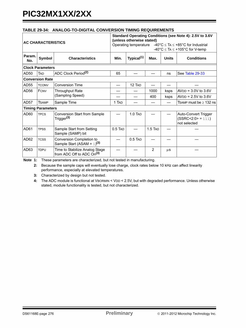
PIC32MX1XX/2XX
TABLE 29-34: ANALOG-TO-DIGITAL CONVERSION TIMING REQUIREMENTS
AC CHARACTERISTICS
Standard Operating Conditions (see Note 4): 2.5V to 3.6V(unless otherwise stated)Operating temperature -40°C TA +85°C for Industrial
-40°C TA +105°C for V-temp
Param. No.
Symbol Characteristics Min. Typical(1) Max. Units Conditions
Clock Parameters
AD50 TAD ADC Clock Period(2) 65 — — ns See Table 29-33
Conversion Rate
AD55 TCONV Conversion Time — 12 TAD — — —
AD56 FCNV Throughput Rate (Sampling Speed)
— — 1000 ksps AVDD = 3.0V to 3.6V
— — 400 ksps AVDD = 2.5V to 3.6V
AD57 TSAMP Sample Time 1 TAD — — — TSAMP must be 132 ns
Timing Parameters
AD60 TPCS Conversion Start from SampleTrigger(3)
— 1.0 TAD — — Auto-Convert Trigger (SSRC<2:0> = 111) not selected
AD61 TPSS Sample Start from SettingSample (SAMP) bit
0.5 TAD — 1.5 TAD — —
AD62 TCSS Conversion Completion toSample Start (ASAM = 1)(3)
— 0.5 TAD — — —
AD63 TDPU Time to Stabilize Analog Stage from ADC Off to ADC On(3)
— — 2 s —
Note 1: These parameters are characterized, but not tested in manufacturing.
2: Because the sample caps will eventually lose charge, clock rates below 10 kHz can affect linearity performance, especially at elevated temperatures.
3: Characterized by design but not tested.
4: The ADC module is functional at VBORMIN < VDD < 2.5V, but with degraded performance. Unless otherwise stated, module functionality is tested, but not characterized.
DS61168E-page 276 Preliminary 2011-2012 Microchip Technology Inc.
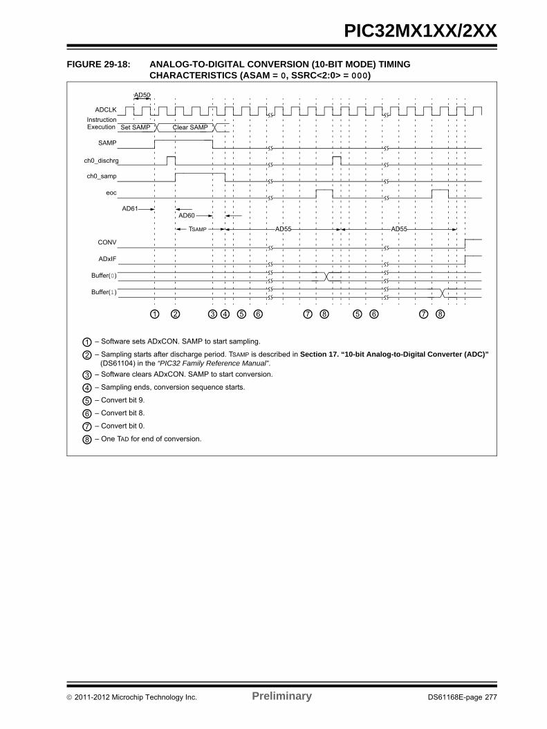
PIC32MX1XX/2XX
FIGURE 29-18: ANALOG-TO-DIGITAL CONVERSION (10-BIT MODE) TIMING CHARACTERISTICS (ASAM = 0, SSRC<2:0> = 000)
AD55TSAMP
Clear SAMPSet SAMP
AD61
ADCLK
Instruction
SAMP
ch0_dischrg
AD60
CONV
ADxIF
Buffer(0)
Buffer(1)
1 2 3 4 5 6 8 5 6 7
1 – Software sets ADxCON. SAMP to start sampling.
2 – Sampling starts after discharge period. TSAMP is described in Section 17. “10-bit Analog-to-Digital Converter (ADC)”
3 – Software clears ADxCON. SAMP to start conversion.
4 – Sampling ends, conversion sequence starts.
5 – Convert bit 9.
8 – One TAD for end of conversion.
AD50
ch0_samp
eoc
7
AD55
8
6 – Convert bit 8.
7 – Convert bit 0.
Execution
(DS61104) in the “PIC32 Family Reference Manual”.
2011-2012 Microchip Technology Inc. Preliminary DS61168E-page 277
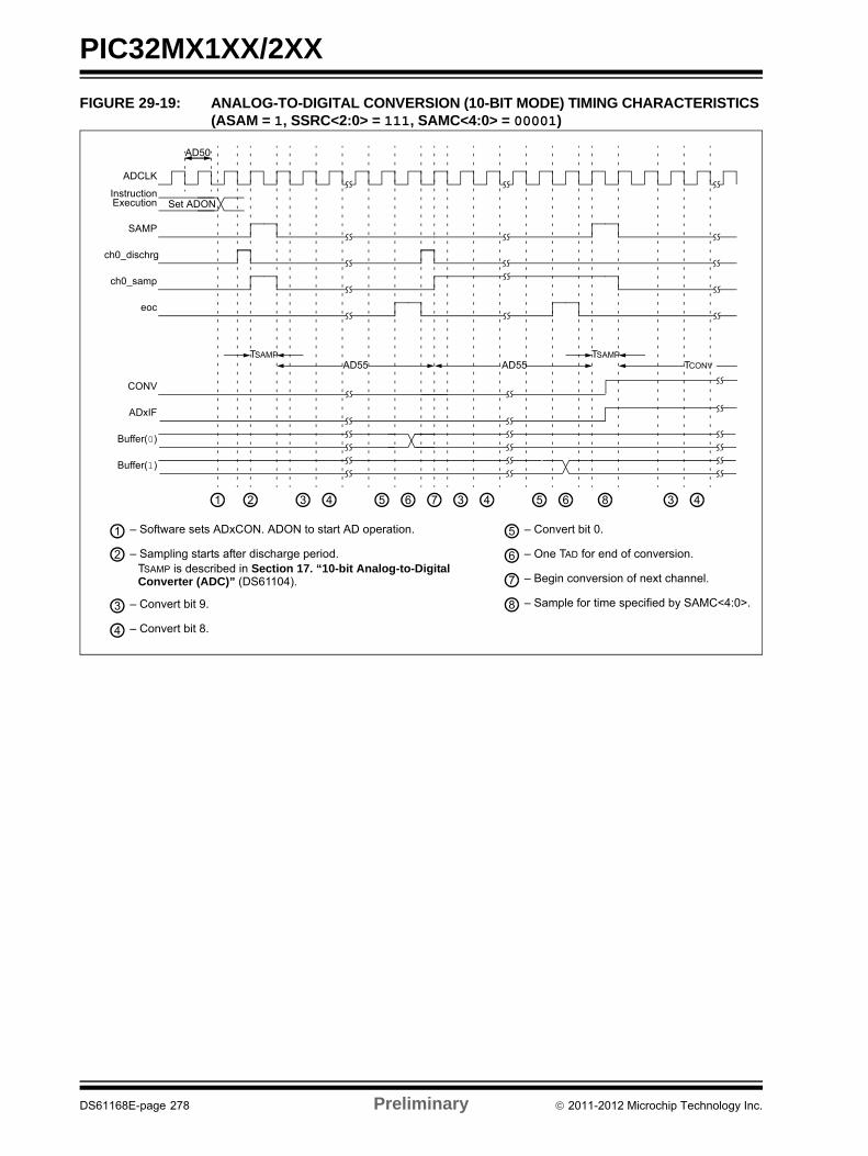
PIC32MX1XX/2XX
FIGURE 29-19: ANALOG-TO-DIGITAL CONVERSION (10-BIT MODE) TIMING CHARACTERISTICS (ASAM = 1, SSRC<2:0> = 111, SAMC<4:0> = 00001)
AD55TSAMP
Set ADON
ADCLK
Instruction
SAMP
ch0_dischrg
CONV
ADxIF
Buffer(0)
Buffer(1)
1 2 3 4 5 6 4 5 6 8
1 – Software sets ADxCON. ADON to start AD operation.
2 – Sampling starts after discharge period.
3 – Convert bit 9.
4 – Convert bit 8.
5 – Convert bit 0.
AD50
ch0_samp
eoc
7 3
AD55
6 – One TAD for end of conversion.
7 – Begin conversion of next channel.
8 – Sample for time specified by SAMC<4:0>.
TSAMPTCONV
3 4
Execution
TSAMP is described in Section 17. “10-bit Analog-to-Digital Converter (ADC)” (DS61104).
DS61168E-page 278 Preliminary 2011-2012 Microchip Technology Inc.
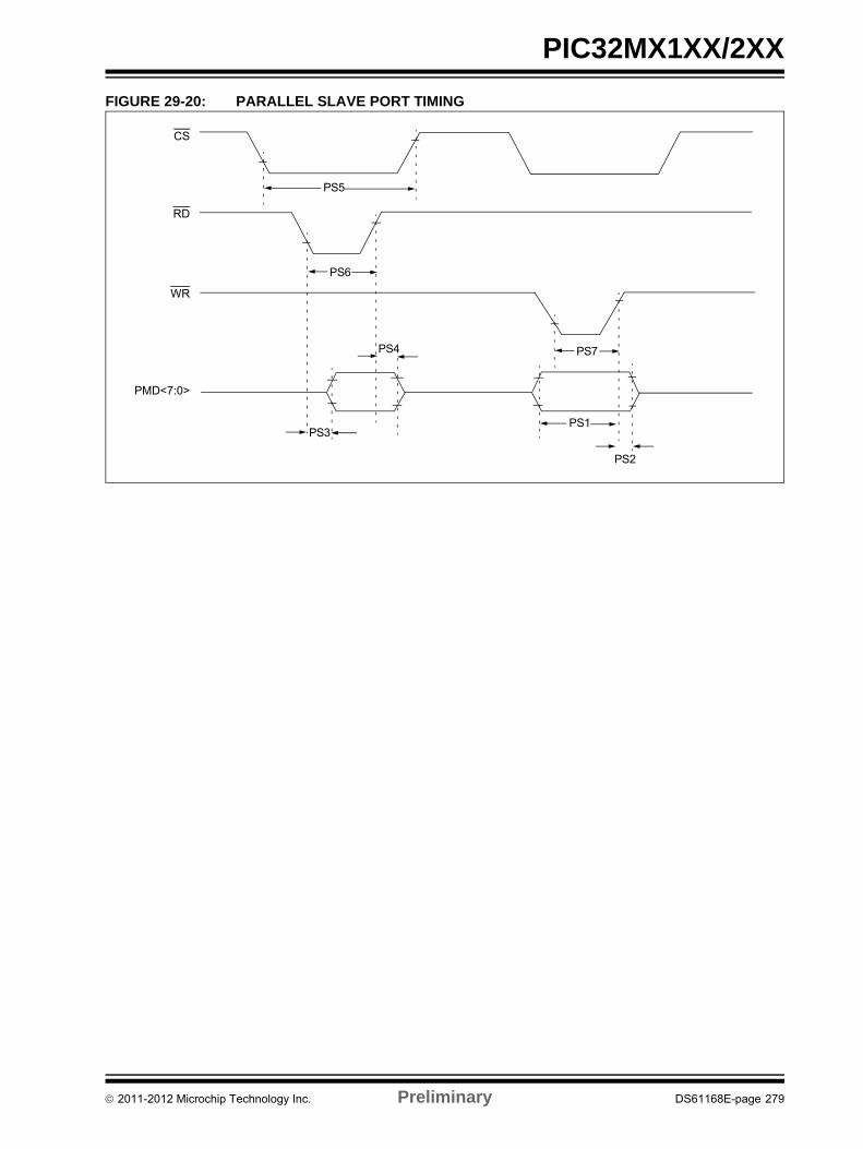
PIC32MX1XX/2XX
FIGURE 29-20: PARALLEL SLAVE PORT TIMING
CS
RD
WR
PMD<7:0>
PS1
PS2
PS3
PS4
PS5
PS6
PS7
2011-2012 Microchip Technology Inc. Preliminary DS61168E-page 279
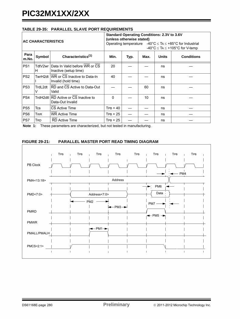
PIC32MX1XX/2XX
FIGURE 29-21: PARALLEL MASTER PORT READ TIMING DIAGRAM
TABLE 29-35: PARALLEL SLAVE PORT REQUIREMENTS
AC CHARACTERISTICS
Standard Operating Conditions: 2.3V to 3.6V(unless otherwise stated)Operating temperature -40°C TA +85°C for Industrial
-40°C TA +105°C for V-temp
Param.No.
Symbol Characteristics(1) Min. Typ. Max. Units Conditions
PS1 TdtV2wrH
Data In Valid before WR or CS Inactive (setup time)
20 — — ns —
PS2 TwrH2dtI
WR or CS Inactive to Data-In Invalid (hold time)
40 — — ns —
PS3 TrdL2dtV
RD and CS Active to Data-Out Valid
— — 60 ns —
PS4 TrdH2dtI RD Activeor CS Inactive to Data-Out Invalid
0 — 10 ns —
PS5 Tcs CS Active Time TPB + 40 — — ns —
PS6 TWR WR Active Time TPB + 25 — — ns —
PS7 TRD RD Active Time TPB + 25 — — ns —
Note 1: These parameters are characterized, but not tested in manufacturing.
TPB TPB TPB TPB TPB TPB TPB TPB
PB Clock
PMALL/PMALH
PMD<7:0>
PMA<13:18>
PMRD
PMCS<2:1>
PMWR
PM5
DataAddress<7:0>
PM1
PM3
PM6
Data
PM7
Address<7:0>
Address
PM4
PM2
DS61168E-page 280 Preliminary 2011-2012 Microchip Technology Inc.
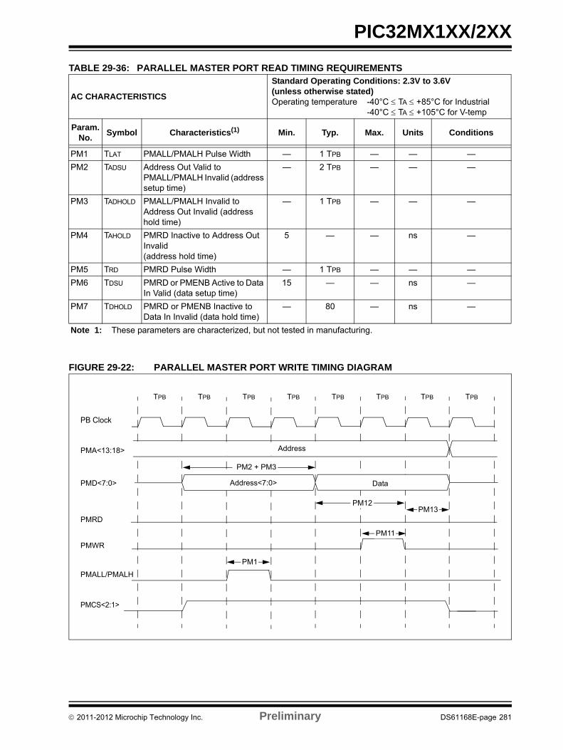
PIC32MX1XX/2XX
FIGURE 29-22: PARALLEL MASTER PORT WRITE TIMING DIAGRAM
TABLE 29-36: PARALLEL MASTER PORT READ TIMING REQUIREMENTS
AC CHARACTERISTICS
Standard Operating Conditions: 2.3V to 3.6V(unless otherwise stated)Operating temperature -40°C TA +85°C for Industrial
-40°C TA +105°C for V-temp
Param. No.
Symbol Characteristics(1) Min. Typ. Max. Units Conditions
PM1 TLAT PMALL/PMALH Pulse Width — 1 TPB — — —
PM2 TADSU Address Out Valid to PMALL/PMALH Invalid (address setup time)
— 2 TPB — — —
PM3 TADHOLD PMALL/PMALH Invalid to Address Out Invalid (address hold time)
— 1 TPB — — —
PM4 TAHOLD PMRD Inactive to Address Out Invalid(address hold time)
5 — — ns —
PM5 TRD PMRD Pulse Width — 1 TPB — — —
PM6 TDSU PMRD or PMENB Active to Data In Valid (data setup time)
15 — — ns —
PM7 TDHOLD PMRD or PMENB Inactive to Data In Invalid (data hold time)
— 80 — ns —
Note 1: These parameters are characterized, but not tested in manufacturing.
TPB TPB TPB TPB TPB TPB TPB TPB
PB Clock
PMALL/PMALH
PMD<7:0>
PMA<13:18>
PMWR
PMCS<2:1>
PMRD
PM12PM13
PM11
Address
Address<7:0> Data
PM2 + PM3
PM1
2011-2012 Microchip Technology Inc. Preliminary DS61168E-page 281
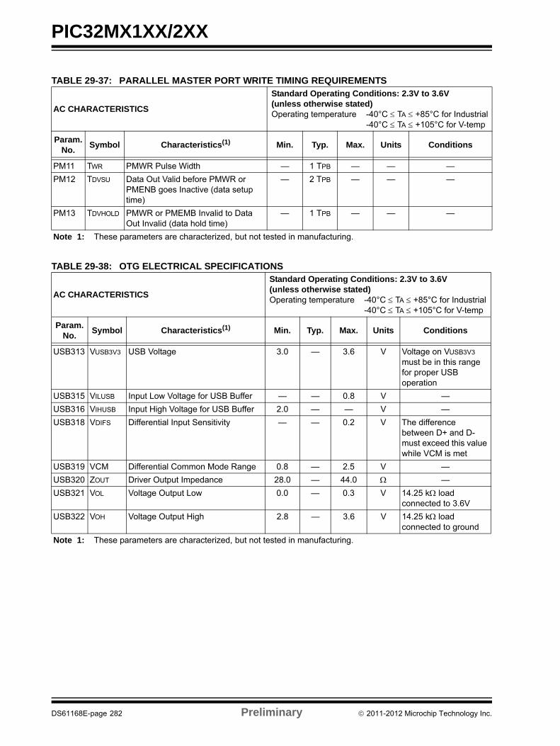
PIC32MX1XX/2XX
TABLE 29-37: PARALLEL MASTER PORT WRITE TIMING REQUIREMENTS
AC CHARACTERISTICS
Standard Operating Conditions: 2.3V to 3.6V(unless otherwise stated)Operating temperature -40°C TA +85°C for Industrial
-40°C TA +105°C for V-temp
Param. No.
Symbol Characteristics(1) Min. Typ. Max. Units Conditions
PM11 TWR PMWR Pulse Width — 1 TPB — — —
PM12 TDVSU Data Out Valid before PMWR or PMENB goes Inactive (data setup time)
— 2 TPB — — —
PM13 TDVHOLD PMWR or PMEMB Invalid to Data Out Invalid (data hold time)
— 1 TPB — — —
Note 1: These parameters are characterized, but not tested in manufacturing.
TABLE 29-38: OTG ELECTRICAL SPECIFICATIONS
AC CHARACTERISTICS
Standard Operating Conditions: 2.3V to 3.6V(unless otherwise stated)Operating temperature -40°C TA +85°C for Industrial
-40°C TA +105°C for V-temp
Param. No.
Symbol Characteristics(1) Min. Typ. Max. Units Conditions
USB313 VUSB3V3 USB Voltage 3.0 — 3.6 V Voltage on VUSB3V3 must be in this range for proper USB operation
USB315 VILUSB Input Low Voltage for USB Buffer — — 0.8 V —
USB316 VIHUSB Input High Voltage for USB Buffer 2.0 — — V —
USB318 VDIFS Differential Input Sensitivity — — 0.2 V The difference between D+ and D- must exceed this value while VCM is met
USB319 VCM Differential Common Mode Range 0.8 — 2.5 V —
USB320 ZOUT Driver Output Impedance 28.0 — 44.0 —
USB321 VOL Voltage Output Low 0.0 — 0.3 V 14.25 k load connected to 3.6V
USB322 VOH Voltage Output High 2.8 — 3.6 V 14.25 k load connected to ground
Note 1: These parameters are characterized, but not tested in manufacturing.
DS61168E-page 282 Preliminary 2011-2012 Microchip Technology Inc.
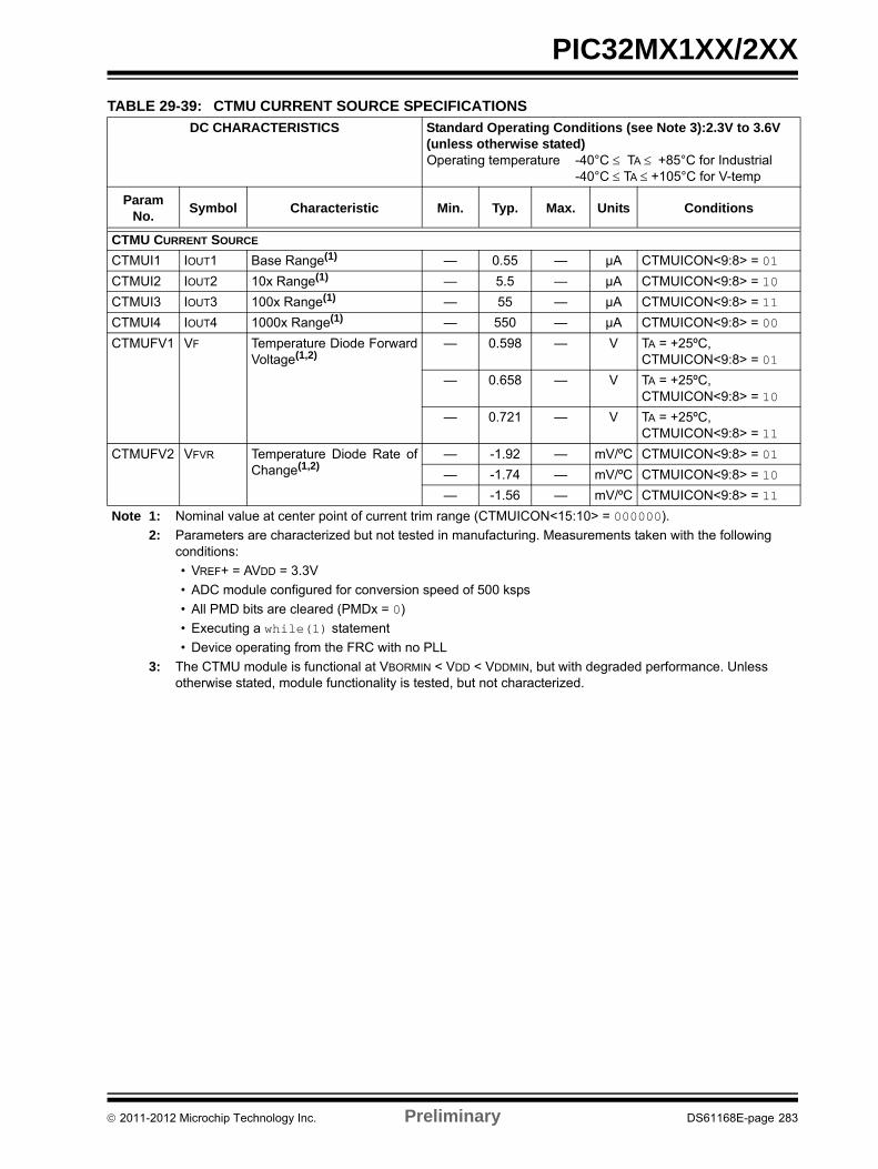
PIC32MX1XX/2XX
TABLE 29-39: CTMU CURRENT SOURCE SPECIFICATIONS
DC CHARACTERISTICS Standard Operating Conditions (see Note 3):2.3V to 3.6V(unless otherwise stated)Operating temperature -40°C TA +85°C for Industrial
-40°C TA +105°C for V-temp
Param No.
Symbol Characteristic Min. Typ. Max. Units Conditions
CTMU CURRENT SOURCE
CTMUI1 IOUT1 Base Range(1) — 0.55 — µA CTMUICON<9:8> = 01
CTMUI2 IOUT2 10x Range(1) — 5.5 — µA CTMUICON<9:8> = 10
CTMUI3 IOUT3 100x Range(1) — 55 — µA CTMUICON<9:8> = 11
CTMUI4 IOUT4 1000x Range(1) — 550 — µA CTMUICON<9:8> = 00
CTMUFV1 VF Temperature Diode ForwardVoltage(1,2)
— 0.598 — V TA = +25ºC, CTMUICON<9:8> = 01
— 0.658 — V TA = +25ºC, CTMUICON<9:8> = 10
— 0.721 — V TA = +25ºC, CTMUICON<9:8> = 11
CTMUFV2 VFVR Temperature Diode Rate ofChange(1,2)
— -1.92 — mV/ºC CTMUICON<9:8> = 01
— -1.74 — mV/ºC CTMUICON<9:8> = 10
— -1.56 — mV/ºC CTMUICON<9:8> = 11
Note 1: Nominal value at center point of current trim range (CTMUICON<15:10> = 000000).
2: Parameters are characterized but not tested in manufacturing. Measurements taken with the following conditions:
• VREF+ = AVDD = 3.3V
• ADC module configured for conversion speed of 500 ksps
• All PMD bits are cleared (PMDx = 0)
• Executing a while(1) statement
• Device operating from the FRC with no PLL
3: The CTMU module is functional at VBORMIN < VDD < VDDMIN, but with degraded performance. Unless otherwise stated, module functionality is tested, but not characterized.
2011-2012 Microchip Technology Inc. Preliminary DS61168E-page 283
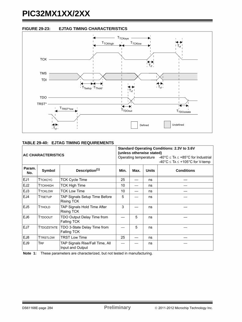
PIC32MX1XX/2XX
FIGURE 29-23: EJTAG TIMING CHARACTERISTICS
TTCKeye
TTCKhigh TTCKlowTrf
Trf
TrfTrf
TTsetup TThold
TTDOout TTDOzstate
Defined Undefined
TTRST*low
Trf
TCK
TDO
TRST*
TDI
TMS
TABLE 29-40: EJTAG TIMING REQUIREMENTS
AC CHARACTERISTICS
Standard Operating Conditions: 2.3V to 3.6V(unless otherwise stated)Operating temperature -40°C TA +85°C for Industrial
-40°C TA +105°C for V-temp
Param.No.
Symbol Description(1) Min. Max. Units Conditions
EJ1 TTCKCYC TCK Cycle Time 25 — ns —
EJ2 TTCKHIGH TCK High Time 10 — ns —
EJ3 TTCKLOW TCK Low Time 10 — ns —
EJ4 TTSETUP TAP Signals Setup Time Before Rising TCK
5 — ns —
EJ5 TTHOLD TAP Signals Hold Time After Rising TCK
3 — ns —
EJ6 TTDOOUT TDO Output Delay Time from Falling TCK
— 5 ns —
EJ7 TTDOZSTATE TDO 3-State Delay Time from Falling TCK
— 5 ns —
EJ8 TTRSTLOW TRST Low Time 25 — ns —
EJ9 TRF TAP Signals Rise/Fall Time, All Input and Output
— — ns —
Note 1: These parameters are characterized, but not tested in manufacturing.
DS61168E-page 284 Preliminary 2011-2012 Microchip Technology Inc.
PIC32MX1XX/2XX
30.0 50 MHz ELECTRICAL CHARACTERISTICS
This section provides an overview of the PIC32MX1XX/2XX electrical characteristics for devices operating at 50 MHz.
The specifications for 50 MHz are identical to those shown in Section 29.0 “Electrical Characteristics”, with theexception of the parameters listed in this chapter.
Parameters in this chapter begin with the letter “M”, which denotes 50 MHz operation. For example, parameter DC29ain Section 29.0 “Electrical Characteristics”, is the up to 40 MHz operation equivalent for MDC29a.
Absolute maximum ratings for the PIC32MX1XX/2XX 50 MHz devices are listed below. Exposure to these maximumrating conditions for extended periods may affect device reliability. Functional operation of the device at these or anyother conditions, above the parameters indicated in the operation listings of this specification, is not implied.
Absolute Maximum Ratings(See Note 1)
Ambient temperature under bias.............................................................................................................. .-40°C to +85°C
Storage temperature .............................................................................................................................. -65°C to +150°C
Voltage on VDD with respect to VSS ......................................................................................................... -0.3V to +4.0V
Voltage on any pin that is not 5V tolerant, with respect to VSS (Note 3)......................................... -0.3V to (VDD + 0.3V)
Voltage on any 5V tolerant pin with respect to VSS when VDD 2.3V (Note 3) ........................................ -0.3V to +5.5V
Voltage on any 5V tolerant pin with respect to VSS when VDD < 2.3V (Note 3)........................................ -0.3V to +3.6V
Voltage on D+ or D- pin with respect to VUSB3V3 ..................................................................... -0.3V to (VUSB3V3 + 0.3V)
Voltage on VBUS with respect to VSS ....................................................................................................... -0.3V to +5.5V
Maximum current out of VSS pin(s) .......................................................................................................................300 mA
Maximum current into VDD pin(s) (Note 2)............................................................................................................300 mA
Maximum output current sunk by any I/O pin..........................................................................................................15 mA
Maximum output current sourced by any I/O pin ....................................................................................................15 mA
Maximum current sunk by all ports .......................................................................................................................200 mA
Maximum current sourced by all ports (Note 2)....................................................................................................200 mA
Note 1: Stresses above those listed under “Absolute Maximum Ratings” may cause permanent damage to thedevice. This is a stress rating only and functional operation of the device at those or any other conditions,above those indicated in the operation listings of this specification, is not implied. Exposure to maximumrating conditions for extended periods may affect device reliability.
2: Maximum allowable current is a function of device maximum power dissipation (see Table 29-2).
3: See the “Pin Diagrams” section for the 5V tolerant pins.
2011-2012 Microchip Technology Inc. Preliminary DS61168E-page 285
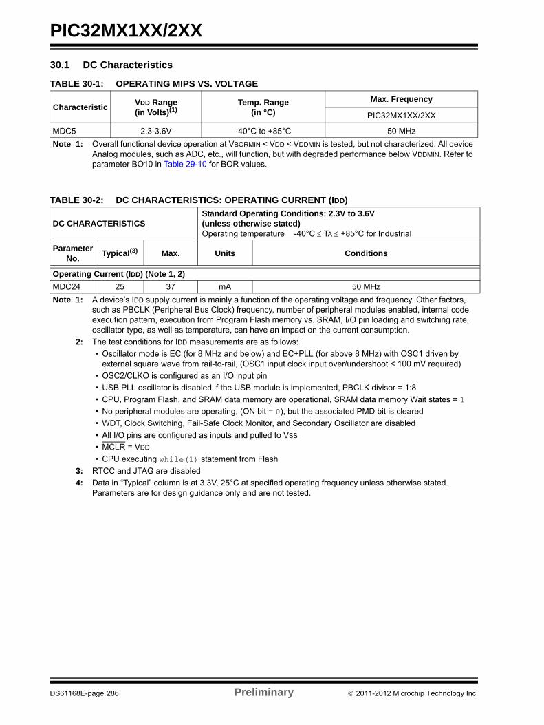
PIC32MX1XX/2XX
30.1 DC Characteristics
TABLE 30-2: DC CHARACTERISTICS: OPERATING CURRENT (IDD)
TABLE 30-1: OPERATING MIPS VS. VOLTAGE
CharacteristicVDD Range(in Volts)(1)
Temp. Range(in °C)
Max. Frequency
PIC32MX1XX/2XX
MDC5 2.3-3.6V -40°C to +85°C 50 MHz
Note 1: Overall functional device operation at VBORMIN < VDD < VDDMIN is tested, but not characterized. All device Analog modules, such as ADC, etc., will function, but with degraded performance below VDDMIN. Refer to parameter BO10 in Table 29-10 for BOR values.
DC CHARACTERISTICSStandard Operating Conditions: 2.3V to 3.6V(unless otherwise stated)Operating temperature -40°C TA +85°C for Industrial
Parameter No.
Typical(3) Max. Units Conditions
Operating Current (IDD) (Note 1, 2)
MDC24 25 37 mA 50 MHz
Note 1: A device’s IDD supply current is mainly a function of the operating voltage and frequency. Other factors, such as PBCLK (Peripheral Bus Clock) frequency, number of peripheral modules enabled, internal code execution pattern, execution from Program Flash memory vs. SRAM, I/O pin loading and switching rate, oscillator type, as well as temperature, can have an impact on the current consumption.
2: The test conditions for IDD measurements are as follows:
• Oscillator mode is EC (for 8 MHz and below) and EC+PLL (for above 8 MHz) with OSC1 driven by external square wave from rail-to-rail, (OSC1 input clock input over/undershoot < 100 mV required)
• OSC2/CLKO is configured as an I/O input pin
• USB PLL oscillator is disabled if the USB module is implemented, PBCLK divisor = 1:8
• CPU, Program Flash, and SRAM data memory are operational, SRAM data memory Wait states = 1
• No peripheral modules are operating, (ON bit = 0), but the associated PMD bit is cleared
• WDT, Clock Switching, Fail-Safe Clock Monitor, and Secondary Oscillator are disabled
• All I/O pins are configured as inputs and pulled to VSS
• MCLR = VDD
• CPU executing while(1) statement from Flash
3: RTCC and JTAG are disabled
4: Data in “Typical” column is at 3.3V, 25°C at specified operating frequency unless otherwise stated. Parameters are for design guidance only and are not tested.
DS61168E-page 286 Preliminary 2011-2012 Microchip Technology Inc.
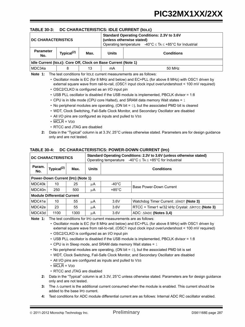
PIC32MX1XX/2XX
TABLE 30-3: DC CHARACTERISTICS: IDLE CURRENT (IIDLE)
DC CHARACTERISTICSStandard Operating Conditions: 2.3V to 3.6V(unless otherwise stated)Operating temperature -40°C TA +85°C for Industrial
Parameter No.
Typical(2) Max. Units Conditions
Idle Current (IIDLE): Core Off, Clock on Base Current (Note 1)
MDC34a 8 13 mA 50 MHz
Note 1: The test conditions for IIDLE current measurements are as follows:
• Oscillator mode is EC (for 8 MHz and below) and EC+PLL (for above 8 MHz) with OSC1 driven by external square wave from rail-to-rail, (OSC1 input clock input over/undershoot < 100 mV required)
• OSC2/CLKO is configured as an I/O input pin
• USB PLL oscillator is disabled if the USB module is implemented, PBCLK divisor = 1:8
• CPU is in Idle mode (CPU core Halted), and SRAM data memory Wait states = 1
• No peripheral modules are operating, (ON bit = 0), but the associated PMD bit is cleared
• WDT, Clock Switching, Fail-Safe Clock Monitor, and Secondary Oscillator are disabled
• All I/O pins are configured as inputs and pulled to VSS
• MCLR = VDD
• RTCC and JTAG are disabled
2: Data in the “Typical” column is at 3.3V, 25°C unless otherwise stated. Parameters are for design guidance only and are not tested.
TABLE 30-4: DC CHARACTERISTICS: POWER-DOWN CURRENT (IPD)
DC CHARACTERISTICSStandard Operating Conditions: 2.3V to 3.6V (unless otherwise stated)Operating temperature -40°C TA +85°C for Industrial
Param. No.
Typical(2) Max. Units Conditions
Power-Down Current (IPD) (Note 1)
MDC40k 10 25 A -40°CBase Power-Down Current
MDC40n 250 500 A +85°C
Module Differential Current
MDC41e 10 55 A 3.6V Watchdog Timer Current: IWDT (Note 3)
MDC42e 23 55 A 3.6V RTCC + Timer1 w/32 kHz Crystal: IRTCC (Note 3)
MDC43d 1100 1300 A 3.6V ADC: IADC (Notes 3,4)
Note 1: The test conditions for IPD current measurements are as follows:• Oscillator mode is EC (for 8 MHz and below) and EC+PLL (for above 8 MHz) with OSC1 driven by
external square wave from rail-to-rail, (OSC1 input clock input over/undershoot < 100 mV required)
• OSC2/CLKO is configured as an I/O input pin
• USB PLL oscillator is disabled if the USB module is implemented, PBCLK divisor = 1:8
• CPU is in Sleep mode, and SRAM data memory Wait states = 1
• No peripheral modules are operating, (ON bit = 0), but the associated PMD bit is set
• WDT, Clock Switching, Fail-Safe Clock Monitor, and Secondary Oscillator are disabled
• All I/O pins are configured as inputs and pulled to VSS
• MCLR = VDD
• RTCC and JTAG are disabled
2: Data in the “Typical” column is at 3.3V, 25°C unless otherwise stated. Parameters are for design guidance only and are not tested.
3: The current is the additional current consumed when the module is enabled. This current should be added to the base IPD current.
4: Test conditions for ADC module differential current are as follows: Internal ADC RC oscillator enabled.
2011-2012 Microchip Technology Inc. Preliminary DS61168E-page 287
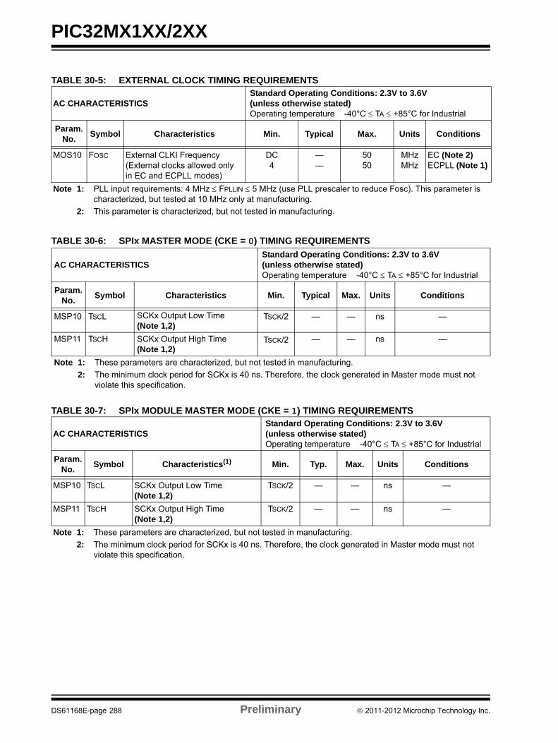
PIC32MX1XX/2XX
TABLE 30-5: EXTERNAL CLOCK TIMING REQUIREMENTS
AC CHARACTERISTICSStandard Operating Conditions: 2.3V to 3.6V(unless otherwise stated)Operating temperature -40°C TA +85°C for Industrial
Param.No.
Symbol Characteristics Min. Typical Max. Units Conditions
MOS10 FOSC External CLKI Frequency(External clocks allowed onlyin EC and ECPLL modes)
DC4
——
5050
MHzMHz
EC (Note 2)ECPLL (Note 1)
Note 1: PLL input requirements: 4 MHz FPLLIN 5 MHz (use PLL prescaler to reduce Fosc). This parameter is characterized, but tested at 10 MHz only at manufacturing.
2: This parameter is characterized, but not tested in manufacturing.
TABLE 30-6: SPIx MASTER MODE (CKE = 0) TIMING REQUIREMENTS
AC CHARACTERISTICSStandard Operating Conditions: 2.3V to 3.6V(unless otherwise stated)Operating temperature -40°C TA +85°C for Industrial
Param.No.
Symbol Characteristics Min. Typical Max. Units Conditions
MSP10 TSCL SCKx Output Low Time (Note 1,2)
TSCK/2 — — ns —
MSP11 TSCH SCKx Output High Time (Note 1,2)
TSCK/2 — — ns —
Note 1: These parameters are characterized, but not tested in manufacturing.
2: The minimum clock period for SCKx is 40 ns. Therefore, the clock generated in Master mode must not violate this specification.
TABLE 30-7: SPIx MODULE MASTER MODE (CKE = 1) TIMING REQUIREMENTS
AC CHARACTERISTICSStandard Operating Conditions: 2.3V to 3.6V(unless otherwise stated)Operating temperature -40°C TA +85°C for Industrial
Param.No.
Symbol Characteristics(1) Min. Typ. Max. Units Conditions
MSP10 TSCL SCKx Output Low Time (Note 1,2)
TSCK/2 — — ns —
MSP11 TSCH SCKx Output High Time (Note 1,2)
TSCK/2 — — ns —
Note 1: These parameters are characterized, but not tested in manufacturing.
2: The minimum clock period for SCKx is 40 ns. Therefore, the clock generated in Master mode must not violate this specification.
DS61168E-page 288 Preliminary 2011-2012 Microchip Technology Inc.
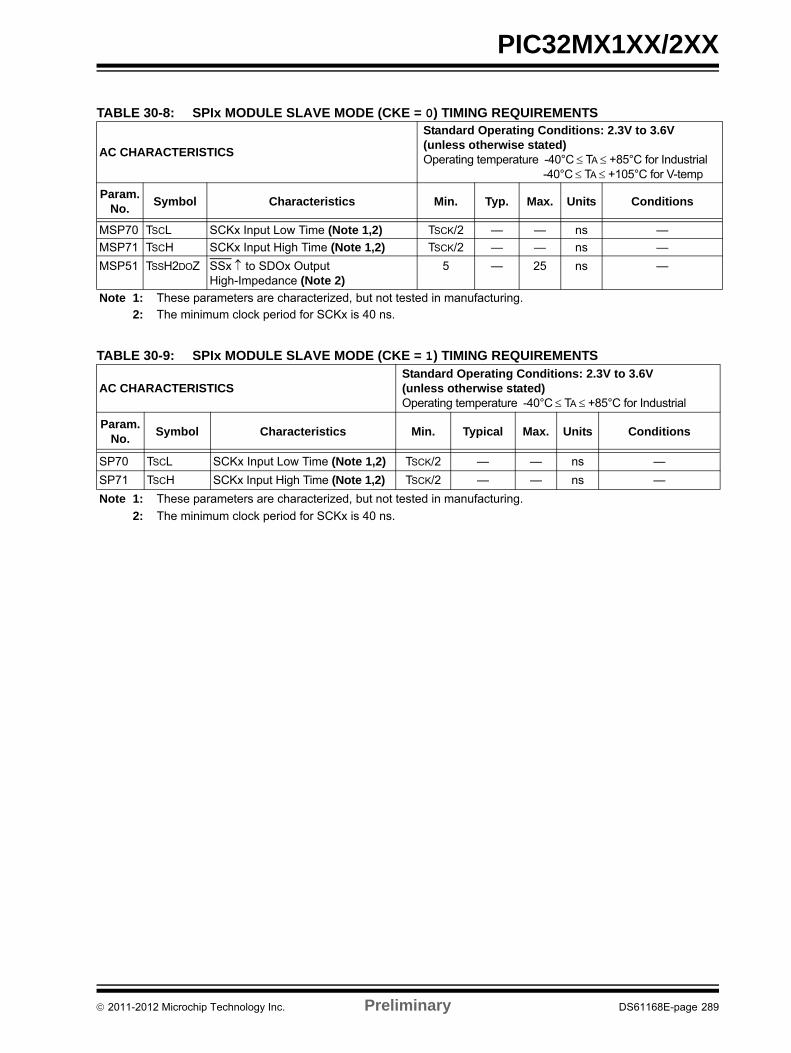
PIC32MX1XX/2XX
TABLE 30-8: SPIx MODULE SLAVE MODE (CKE = 0) TIMING REQUIREMENTS
AC CHARACTERISTICS
Standard Operating Conditions: 2.3V to 3.6V(unless otherwise stated)Operating temperature -40°C TA +85°C for Industrial
-40°C TA +105°C for V-temp
Param.No.
Symbol Characteristics Min. Typ. Max. Units Conditions
MSP70 TSCL SCKx Input Low Time (Note 1,2) TSCK/2 — — ns —
MSP71 TSCH SCKx Input High Time (Note 1,2) TSCK/2 — — ns —
MSP51 TSSH2DOZ SSx to SDOx Output High-Impedance (Note 2)
5 — 25 ns —
Note 1: These parameters are characterized, but not tested in manufacturing.2: The minimum clock period for SCKx is 40 ns.
TABLE 30-9: SPIx MODULE SLAVE MODE (CKE = 1) TIMING REQUIREMENTS
AC CHARACTERISTICSStandard Operating Conditions: 2.3V to 3.6V(unless otherwise stated)Operating temperature -40°C TA +85°C for Industrial
Param.No.
Symbol Characteristics Min. Typical Max. Units Conditions
SP70 TSCL SCKx Input Low Time (Note 1,2) TSCK/2 — — ns —
SP71 TSCH SCKx Input High Time (Note 1,2) TSCK/2 — — ns —
Note 1: These parameters are characterized, but not tested in manufacturing.
2: The minimum clock period for SCKx is 40 ns.
2011-2012 Microchip Technology Inc. Preliminary DS61168E-page 289

PIC32MX1XX/2XX
NOTES:
DS61168E-page 290 Preliminary 2011-2012 Microchip Technology Inc.
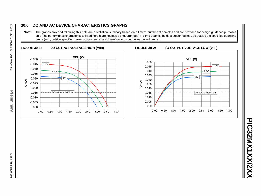
2011
-2012 Microchip T
echnology Inc.
Prelim
ina
ryD
S61168E
-page 291
PIC
32MX
1XX
/2XX
3
F T VOLTAGE LOW (VOL)
re provided for design guidance purposested may be outside the specified operating
VOL�(V)
.50 2.00 2.50 3.00 3.50 4.00
VOL�(V)
3V
3.3V
3.6V
Absolute Maximum
0.0 DC AND AC DEVICE CHARACTERISTICS GRAPHS
IGURE 30-1: I/O OUTPUT VOLTAGE HIGH (VOH) FIGURE 30-2: I/O OUTPU
Note: The graphs provided following this note are a statistical summary based on a limited number of samples and aonly. The performance characteristics listed herein are not tested or guaranteed. In some graphs, the data presenrange (e.g., outside specified power supply range) and therefore, outside the warranted range.
-0.050
-0.045
-0.040
-0.035
-0.030
-0.025
-0.020IOH
(A)
VOH (V)-0.050
-0.045
-0.040
-0.035
-0.030
-0.025
-0.020
-0.015
-0.010
-0.005
0.0000.00 0.50 1.00 1.50 2.00 2.50 3.00 3.50 4.00
IOH
(A)
VOH (V)
3V
3.3V
3.6V
Absolute Maximum 0.0150.0200.0250.0300.0350.0400.0450.050
IOH
(A)
0.0000.0050.0100.0150.0200.0250.0300.0350.0400.0450.050
0.00 0.50 1.00 1
IOH
(A)
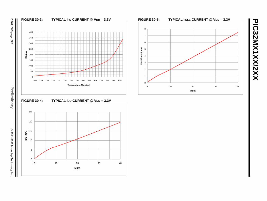
PIC
32MX
1XX
/2XX
DS
61168E-page 292
Prelim
ina
ry
2011-2012 Microchip T
echnology Inc.
FIGURE 30-3: TYPICAL IPD CURRENT @ VDD = 3.3V FIGURE 30-5: TYPICAL IIDLE CURRENT @ VDD = 3.3V
20 30 40
MIPS
FIGURE 30-4: TYPICAL IDD CURRENT @ VDD = 3.3V
150
200
250
300
350
400
IPD
(µA)
0
50
100
150
200
250
300
350
400
-40 -30 -20 -10 0 10 20 30 40 50 60 70 80 90 100
IPD
(µA)
Temperature (Celsius)
10
15
20
25
IDD
(mA)
0
5
10
15
20
25
0 10 20 30 40
IDD
(mA)
MIPS
3
4
5
6
7
8
DLE
Cur
rent
(mA)
0
1
2
0 10
IID
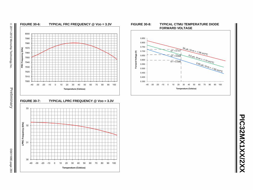
2011
-2012 Microchip T
echnology Inc.
Prelim
ina
ryD
S61168E
-page 293
PIC
32MX
1XX
/2XX
F
F
TMU TEMPERATURE DIODE VOLTAGE
20 30 40 50 60 70 80 90 100 110
Temperature (Celsius)
.598
.658
.72155 µA, VFVR = -1.56 mV/ºC5.5 µA, VFVR = -1.74 mV/ºC0.55 µA, VFVR = -1.92 mV/ºC
IGURE 30-6: TYPICAL FRC FREQUENCY @ VDD = 3.3V
IGURE 30-7: TYPICAL LPRC FREQUENCY @ VDD = 3.3V
FIGURE 30-8: TYPICAL CFORWARD
7930
7940
7950
7960
7970
7980
7990
8000
FRC
Fre
quen
cy (k
Hz)
7900
7910
7920
7930
7940
7950
7960
7970
7980
7990
8000
-40 -30 -20 -10 0 10 20 30 40 50 60 70 80 90 100
FRC
Fre
quen
cy (k
Hz)
Temperature (Celsius)
31
32
33
LPR
C F
requ
ency
(kH
z)
30
31
32
33
-40 -30 -20 -10 0 10 20 30 40 50 60 70 80 90 100
LPR
C F
requ
ency
(kH
z)
Temperature (Celsius)
0 500
0.550
0.600
0.650
0.700
0.750
0.800
0.850
Forw
ard
Volta
ge (V
)
0.350
0.400
0.450
0.500
0.550
0.600
0.650
0.700
0.750
0.800
0.850
-40 -30 -20 -10 0 10
Forw
ard
Volta
ge (V
)
VF = 0
VF = 0
VF = 0

PIC32MX1XX/2XX
NOTES:
DS61168E-page 294 Preliminary 2011-2012 Microchip Technology Inc.
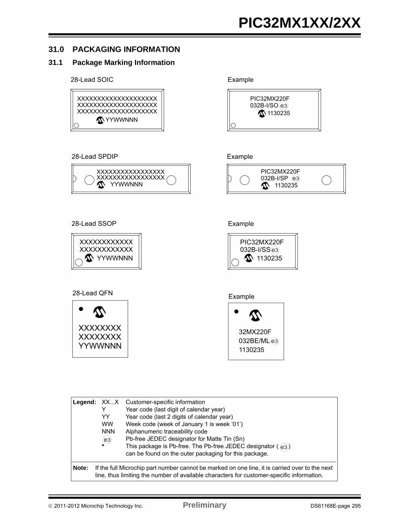
PIC32MX1XX/2XX
31.0 PACKAGING INFORMATION
31.1 Package Marking Information
Legend: XX...X Customer-specific informationY Year code (last digit of calendar year)YY Year code (last 2 digits of calendar year)WW Week code (week of January 1 is week ‘01’)NNN Alphanumeric traceability code Pb-free JEDEC designator for Matte Tin (Sn)* This package is Pb-free. The Pb-free JEDEC designator ( )
can be found on the outer packaging for this package.
Note: If the full Microchip part number cannot be marked on one line, it is carried over to the nextline, thus limiting the number of available characters for customer-specific information.
3e
3e
Example
32MX220F032BE/ML1130235
3e
28-Lead SSOP
XXXXXXXXXXXXXXXXXXXXXXXX
YYWWNNN
Example
PIC32MX220F032B-I/SS
11302353e
28-Lead SOIC
XXXXXXXXXXXXXXXXXXXXXXXXXXXXXXXXXXXXXXXXXXXXXXXXXXXXXXXXXXXX
YYWWNNN
Example
PIC32MX220F
1130235032B-I/SO 3e
28-Lead QFN
XXXXXXXXXXXXXXXXYYWWNNN
28-Lead SPDIP
XXXXXXXXXXXXXXXXXXXXXXXXXXXXXXXXXX
YYWWNNN
Example
PIC32MX220F
1130235032B-I/SP 3e
2011-2012 Microchip Technology Inc. Preliminary DS61168E-page 295
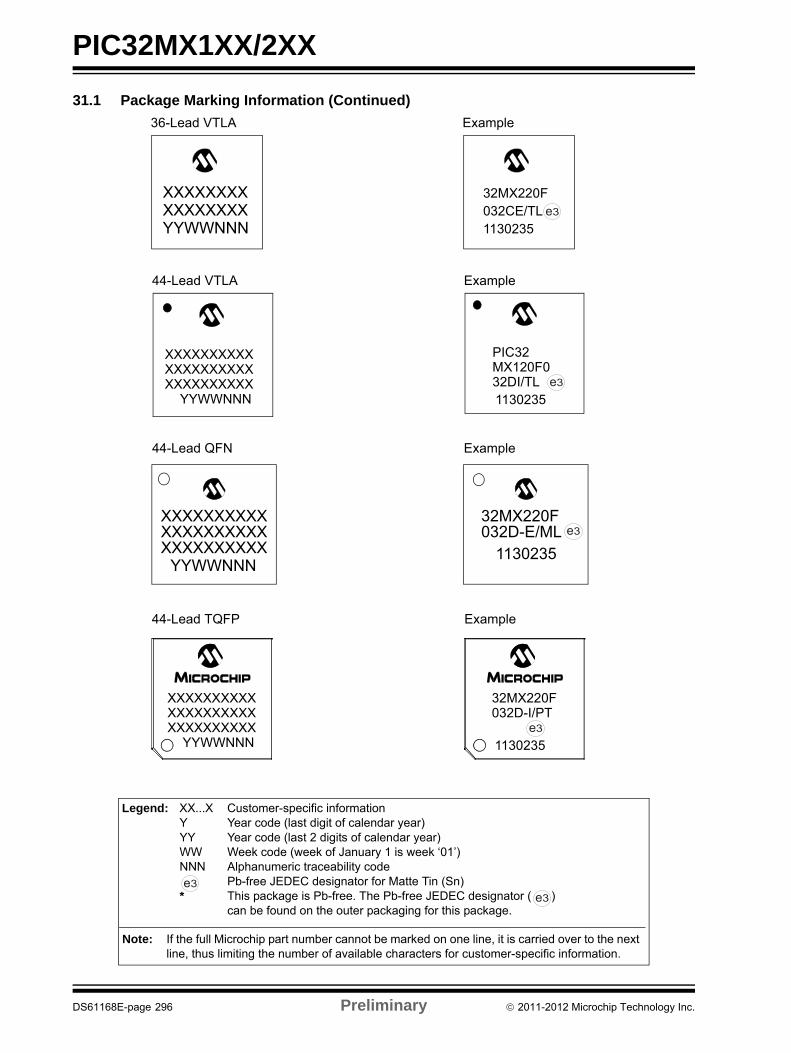
PIC32MX1XX/2XX
31.1 Package Marking Information (Continued)
XXXXXXXXXX
44-Lead QFN
XXXXXXXXXXXXXXXXXXXX
YYWWNNN
32MX220F
Example
032D-E/ML1130235
44-Lead TQFP
XXXXXXXXXXXXXXXXXXXXXXXXXXXXXX
YYWWNNN
Example
32MX220F032D-I/PT
1130235
3e
3e
Legend: XX...X Customer-specific informationY Year code (last digit of calendar year)YY Year code (last 2 digits of calendar year)WW Week code (week of January 1 is week ‘01’)NNN Alphanumeric traceability code Pb-free JEDEC designator for Matte Tin (Sn)* This package is Pb-free. The Pb-free JEDEC designator ( )
can be found on the outer packaging for this package.
Note: If the full Microchip part number cannot be marked on one line, it is carried over to the nextline, thus limiting the number of available characters for customer-specific information.
3e
3e
36-Lead VTLA
XXXXXXXXXXXXXXXXYYWWNNN
Example
32MX220F032CE/TL1130235
3e
44-Lead VTLA Example
XXXXXXXXXXXXXXXXXXXXXXXXXXXXXX
YYWWNNN
PIC32MX120F0
11302353e32DI/TL
DS61168E-page 296 Preliminary 2011-2012 Microchip Technology Inc.
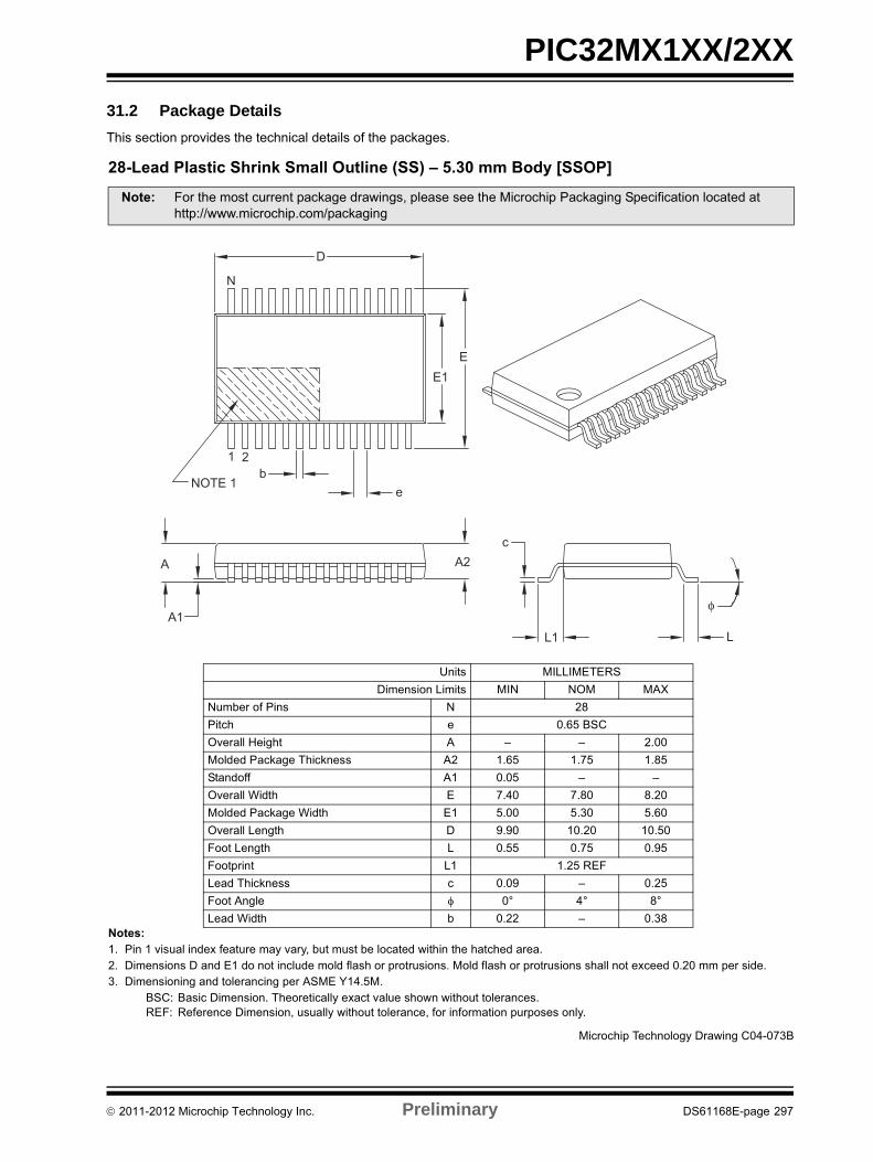
PIC32MX1XX/2XX
31.2 Package Details
This section provides the technical details of the packages.
���������� ��������������� ���������������� �!"���#
$ ��%�� ������ �!"�����# $�% �&"� �'��� ���(�)"&�'"!&�) �����& #�*�&����&� ���&�� #��� ���� ��' �!���!�����#�+��#����&�����"# �'��#�%��!�������&�"!���!�����#�%��!�������&�"!���!�!�������&� $� #������''� ��!�# �,� ��' �!���������#�&�� �������� �����+�-���.��
/�01 /�!�����' �!������� �� &������� $��&� ��" �!��*��*�&��"&�&�� ���� !��+21 � % � �� ���' �!���(�"!"�����*�&��"&�&�� ���� (�%�����%��'�&����"��! !������
$ �% 2���&� �'�!&��"�� �&���3�� �#��*���!(�� �! �! �&� �������������3������� ��%���&��������& #��&��&&144***�'����������'4��3�����
5��&! ��66��+�+����' �!����6�'�&! ��7 78� ��9
7"') ���%����! 7 �:��&�� ���.�/�08 �����; ���& � < < �������# #����3�� �����3� !! �� ���. ���. ��:.�&��#�%%� �� ���. < <8 �����=�#&� + ���� ��:� :������# #����3�� �=�#&� +� .��� .�,� .���8 �����6 ��&� � ���� ����� ���.�2��&�6 ��&� 6 ��.. ���. ���.2��&���& 6� ���.��+26 �#�����3� !! � ���� < ���.2��&����� � �> �> :>6 �#�=�#&� ) ���� < ��,:
LL1
cA2
A1
A
EE1
D
N
1 2
NOTE 1b
e
φ
�������� � �������� ���*��� 0����,/
2011-2012 Microchip Technology Inc. Preliminary DS61168E-page 297
PIC32MX1XX/2XX
Note: For the most current package drawings, please see the Microchip Packaging Specification located at http://www.microchip.com/packaging
DS61168E-page 298 Preliminary 2011-2012 Microchip Technology Inc.
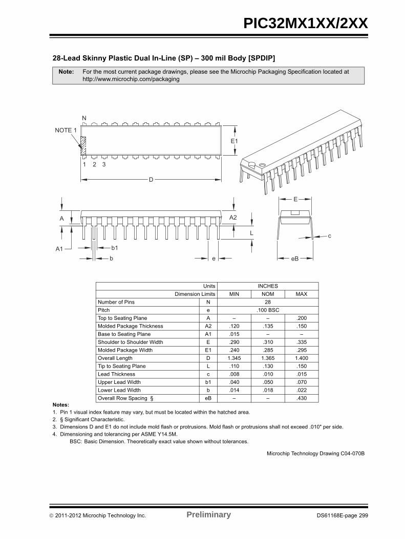
PIC32MX1XX/2XX
������������!��� ��&���'����������������� �!"�&'#
$ ��%�� ������ �!"�����# $�% �&"� �'��� ���(�)"&�'"!&�) �����& #�*�&����&� ���&�� #��� ���� ?������%����&�0�����& ��!&���,� ��' �!���!�����#�+��#����&�����"# �'��#�%��!�������&�"!���!�����#�%��!�������&�"!���!�!�������&� $� #�����@� ��!�# ��� ��' �!���������#�&�� �������� �����+�-���.��
/�01 /�!�����' �!������� �� &������� $��&� ��" �!��*��*�&��"&�&�� ���� !�
$ �% 2���&� �'�!&��"�� �&���3�� �#��*���!(�� �! �! �&� �������������3������� ��%���&��������& #��&��&&144***�'����������'4��3�����
5��&! �70;+���' �!����6�'�&! ��7 78� ��9
7"') ���%����! 7 �:��&�� �����/�0���&��� �&�������� � < < �������# #����3�� �����3� !! �� ���� ��,. ��.�/�! �&��� �&�������� �� ���. < <���"�# ��&�����"�# ��=�#&� + ���� �,�� �,,.���# #����3�� �=�#&� +� ���� ��:. ���.8 �����6 ��&� � ��,�. ��,�. ��������&��� �&�������� 6 ���� ��,� ��.�6 �#�����3� !! � ���: ���� ���.5 ��6 �#�=�#&� )� ���� ��.� ����6�* ��6 �#�=�#&� ) ���� ���: ����8 �������*���������? / < < ��,�
NOTE 1
N
1 2
D
E1
eB
c
E
L
A2
eb
b1A1
A
3
�������� � �������� ���*��� 0�����/
2011-2012 Microchip Technology Inc. Preliminary DS61168E-page 299
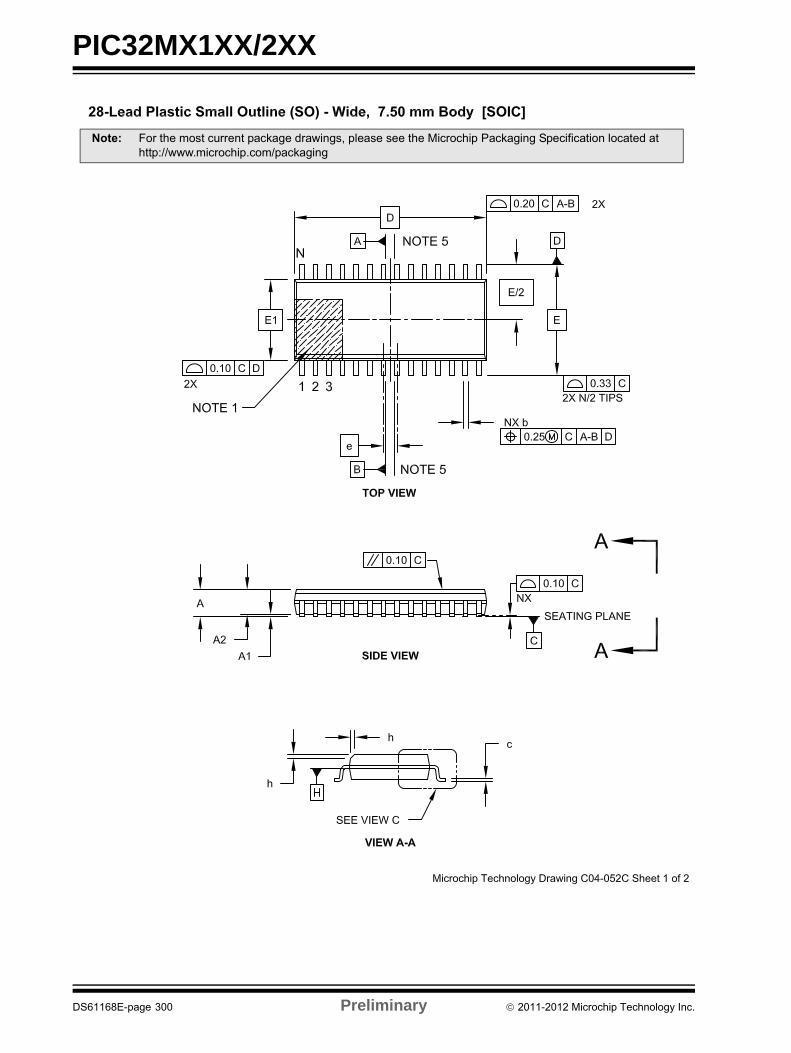
PIC32MX1XX/2XX
Note: For the most current package drawings, please see the Microchip Packaging Specification located at http://www.microchip.com/packaging
DS61168E-page 300 Preliminary 2011-2012 Microchip Technology Inc.
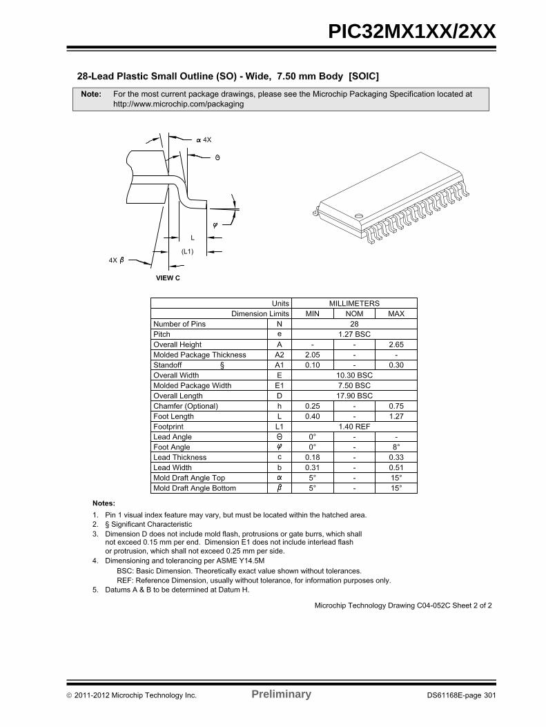
PIC32MX1XX/2XX
Note: For the most current package drawings, please see the Microchip Packaging Specification located at http://www.microchip.com/packaging
2011-2012 Microchip Technology Inc. Preliminary DS61168E-page 301
PIC32MX1XX/2XX
Note: For the most current package drawings, please see the Microchip Packaging Specification located at http://www.microchip.com/packaging
DS61168E-page 302 Preliminary 2011-2012 Microchip Technology Inc.
PIC32MX1XX/2XX
���������� ��(���)�� *$ ��������+��,���-.-��� �!"()$#/� �������0 � �� ���+ �
$ ��%�� ������ �!"�����# $�% �&"� �'��� ���(�)"&�'"!&�) �����& #�*�&����&� ���&�� #��� ���� ���3�� ��!�!�*�!���"��& #�,� ��' �!���������#�&�� �������� �����+�-���.��
/�01 /�!�����' �!������� �� &������� $��&� ��" �!��*��*�&��"&�&�� ���� !��+21 � % � �� ���' �!���(�"!"�����*�&��"&�&�� ���� (�%�����%��'�&����"��! !������
$ �% 2���&� �'�!&��"�� �&���3�� �#��*���!(�� �! �! �&� �������������3������� ��%���&��������& #��&��&&144***�'����������'4��3�����
5��&! ��66��+�+����' �!����6�'�&! ��7 78� ��9
7"') ���%����! 7 �:��&�� ���.�/�08 �����; ���& � ��:� ���� �����&��#�%%� �� ���� ���� ���.0��&��&�����3� !! �, ������+28 �����=�#&� + �����/�0+$�! #���#�=�#&� +� ,��. ,��� ����8 �����6 ��&� � �����/�0+$�! #���#�6 ��&� �� ,��. ,��� ����0��&��&�=�#&� ) ���, ��,� ��,.0��&��&�6 ��&� 6 ��.� ��.. ����0��&��&&�+$�! #���# A ���� < <
D EXPOSED D2
e
b
K
E2
E
L
N
NOTE 1
1
22
1
N
A
A1A3
TOP VIEW BOTTOM VIEW
PAD
�������� � �������� ���*��� 0����./
2011-2012 Microchip Technology Inc. Preliminary DS61168E-page 303
PIC32MX1XX/2XX
���������� ��(���)�� *$ ��������+��,���-.-��� �!"()$#/� �������0 � �� ���+ �
$ �% 2���&� �'�!&��"�� �&���3�� �#��*���!(�� �! �! �&� �������������3������� ��%���&��������& #��&��&&144***�'����������'4��3�����
DS61168E-page 304 Preliminary 2011-2012 Microchip Technology Inc.
PIC32MX1XX/2XX
2011-2012 Microchip Technology Inc. Preliminary DS61168E-page 305
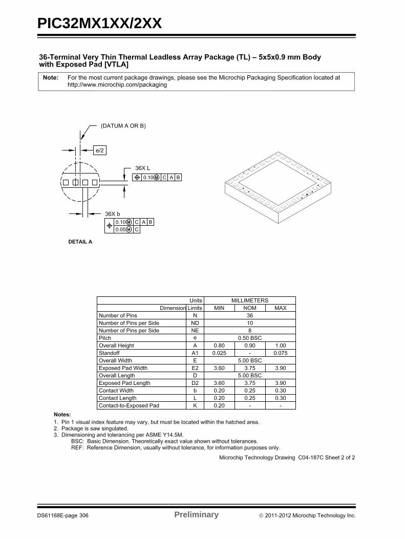
PIC32MX1XX/2XX
DS61168E-page 306 Preliminary 2011-2012 Microchip Technology Inc.
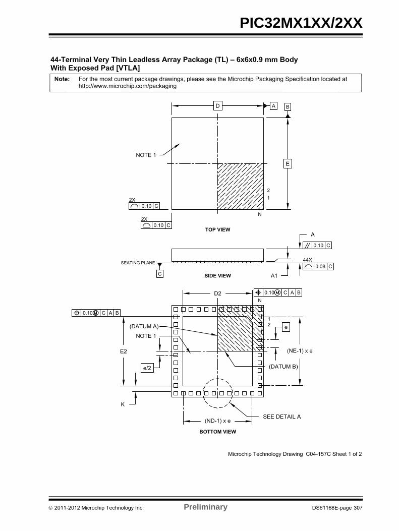
PIC32MX1XX/2XX
2011-2012 Microchip Technology Inc. Preliminary DS61168E-page 307
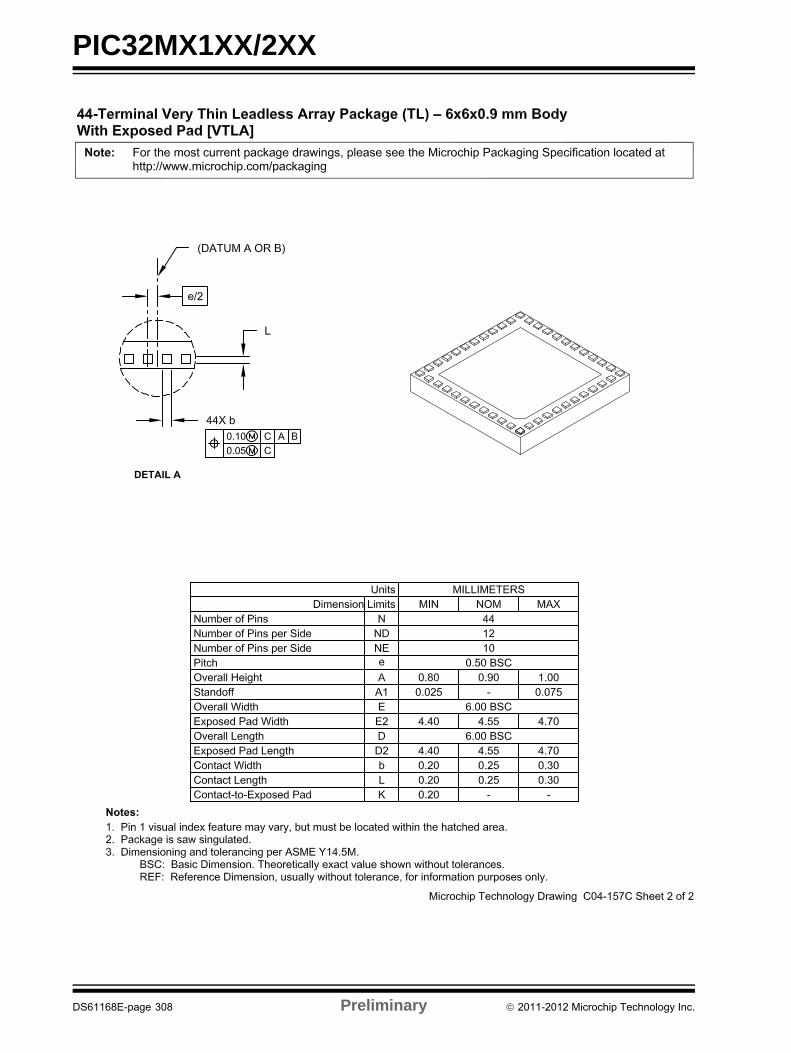
PIC32MX1XX/2XX
DS61168E-page 308 Preliminary 2011-2012 Microchip Technology Inc.
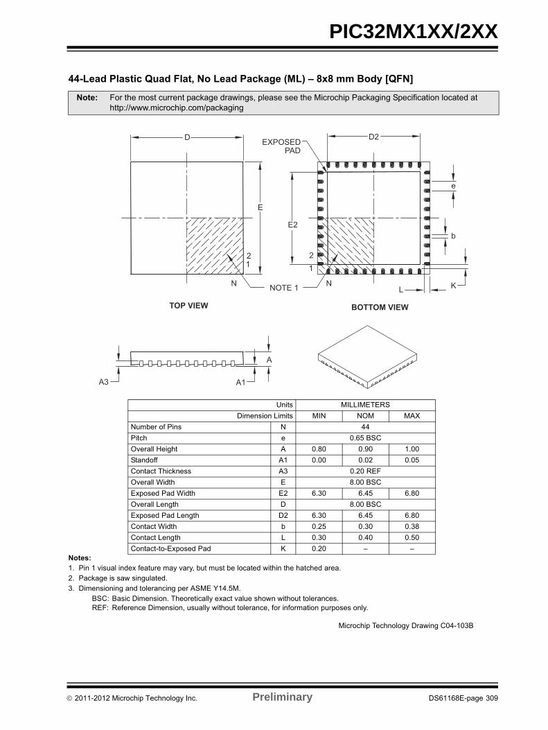
PIC32MX1XX/2XX
11�������� ��(���)�� *$ ��������+��,����.���� �!"()$#
$ ��%�� ������ �!"�����# $�% �&"� �'��� ���(�)"&�'"!&�) �����& #�*�&����&� ���&�� #��� ���� ���3�� ��!�!�*�!���"��& #�,� ��' �!���������#�&�� �������� �����+�-���.��
/�01 /�!�����' �!������� �� &������� $��&� ��" �!��*��*�&��"&�&�� ���� !��+21 � % � �� ���' �!���(�"!"�����*�&��"&�&�� ���� (�%�����%��'�&����"��! !������
$ �% 2���&� �'�!&��"�� �&���3�� �#��*���!(�� �! �! �&� �������������3������� ��%���&��������& #��&��&&144***�'����������'4��3�����
5��&! ��66��+�+����' �!����6�'�&! ��7 78� ��9
7"') ���%����! 7 ����&�� ���.�/�08 �����; ���& � ��:� ���� �����&��#�%%� �� ���� ���� ���.0��&��&�����3� !! �, ������+28 �����=�#&� + :����/�0+$�! #���#�=�#&� +� ��,� ���. ��:�8 �����6 ��&� � :����/�0+$�! #���#�6 ��&� �� ��,� ���. ��:�0��&��&�=�#&� ) ���. ��,� ��,:0��&��&�6 ��&� 6 ��,� ���� ��.�0��&��&&�+$�! #���# A ���� < <
D EXPOSEDPAD
D2
e
b
KL
E2
21
NNOTE 1
21
E
N
BOTTOM VIEWTOP VIEW
A3 A1
A
�������� � �������� ���*��� 0����,/
2011-2012 Microchip Technology Inc. Preliminary DS61168E-page 309
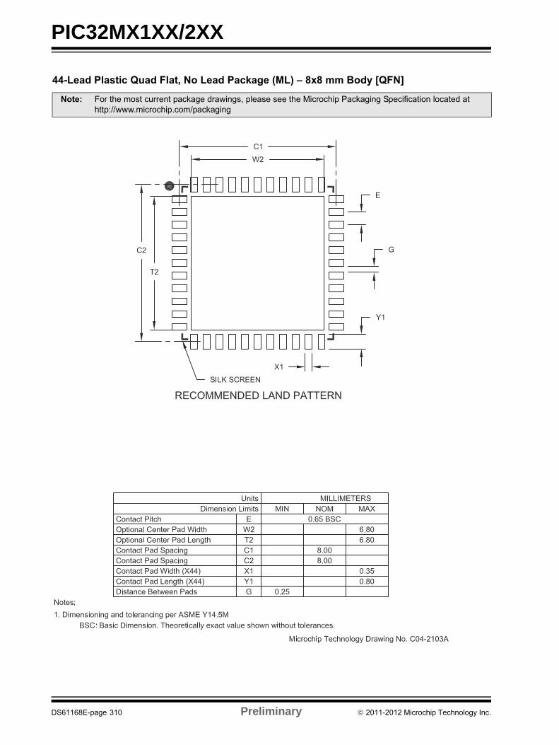
PIC32MX1XX/2XX
11�������� ��(���)�� *$ ��������+��,����.���� �!"()$#
$ �% 2���&� �'�!&��"�� �&���3�� �#��*���!(�� �! �! �&� �������������3������� ��%���&��������& #��&��&&144***�'����������'4��3�����
DS61168E-page 310 Preliminary 2011-2012 Microchip Technology Inc.
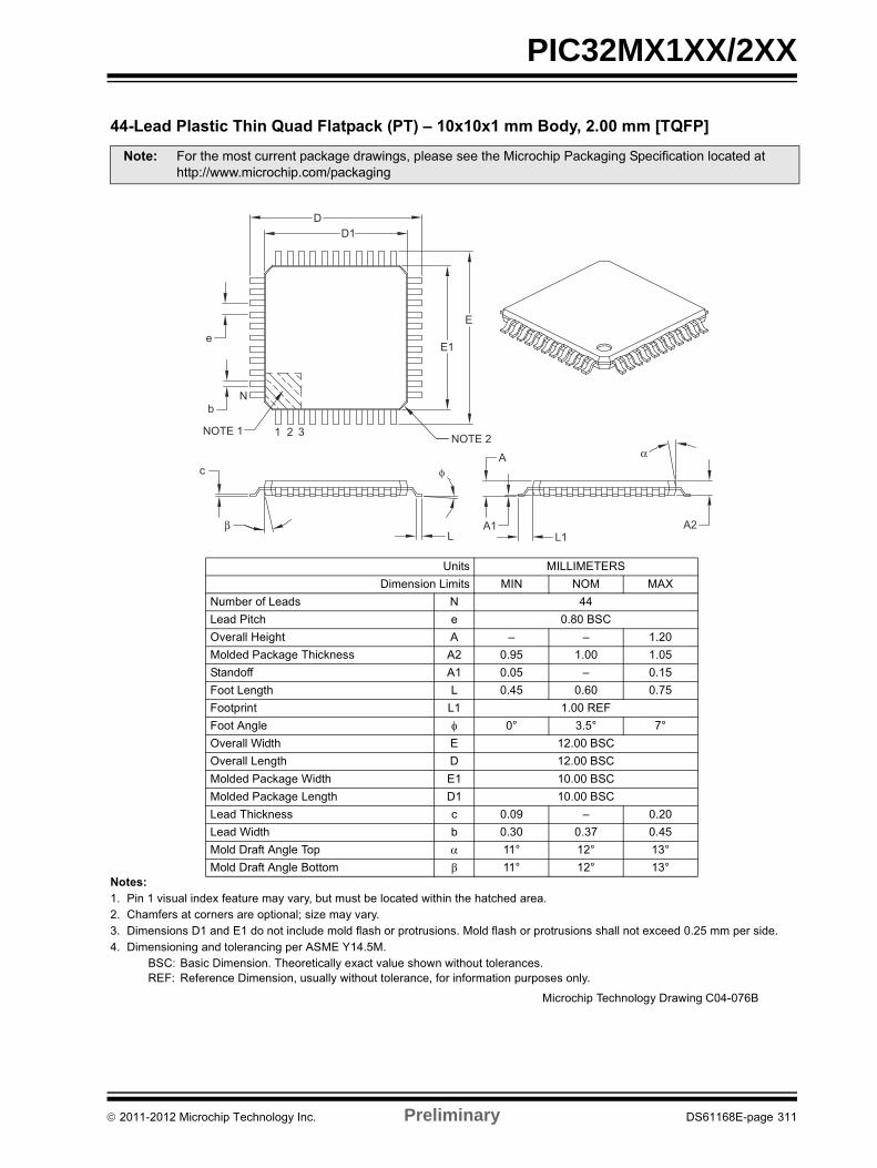
PIC32MX1XX/2XX
11�������� ��2���(���)�� 3����2��4�.4�.4��� �!*������"2()#
$ ��%�� ������ �!"�����# $�% �&"� �'��� ���(�)"&�'"!&�) �����& #�*�&����&� ���&�� #��� ���� 0��'% �!��&����� �!��� ��&�����B�!�C �'��� ����,� ��' �!���!������#�+��#����&�����"# �'��#�%��!�������&�"!���!�����#�%��!�������&�"!���!�!�������&� $� #����.�''� ��!�# ��� ��' �!���������#�&�� �������� �����+�-���.��
/�01 /�!�����' �!������� �� &������� $��&� ��" �!��*��*�&��"&�&�� ���� !��+21 � % � �� ���' �!���(�"!"�����*�&��"&�&�� ���� (�%�����%��'�&����"��! !������
$ �% 2���&� �'�!&��"�� �&���3�� �#��*���!(�� �! �! �&� �������������3������� ��%���&��������& #��&��&&144***�'����������'4��3�����
5��&! ��66��+�+����' �!����6�'�&! ��7 78� ��9
7"') ���%�6 �#! 7 ��6 �#���&�� ��:��/�08 �����; ���& � < < �������# #����3�� �����3� !! �� ���. ���� ���.�&��#�%%�� �� ���. < ���.2��&�6 ��&� 6 ���. ���� ���.2��&���& 6� ������+22��&����� � �> ,�.> �>8 �����=�#&� + ������/�08 �����6 ��&� � ������/�0���# #����3�� �=�#&� +� ������/�0���# #����3�� �6 ��&� �� ������/�06 �#�����3� !! � ���� < ����6 �#�=�#&� ) ��,� ��,� ���.���#����%&����� ��� � ��> ��> �,>���#����%&����� �/�&&�' � ��> ��> �,>
A
E
E1
DD1
e
b
NOTE 1NOTE 2
N
1 2 3
c
A1L
A2L1
α
φ
β
�������� � �������� ���*��� 0�����/
2011-2012 Microchip Technology Inc. Preliminary DS61168E-page 311
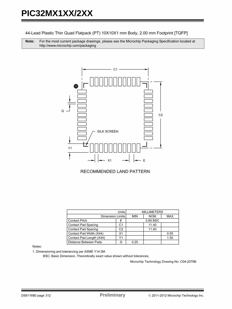
PIC32MX1XX/2XX
Note: For the most current package drawings, please see the Microchip Packaging Specification located at http://www.microchip.com/packaging
DS61168E-page 312 Preliminary 2011-2012 Microchip Technology Inc.
PIC32MX1XX/2XX
APPENDIX A: REVISION HISTORY
Revision A (May 2011)
This is the initial released version of this document.
Revision B (October 2011)
The following two global changes are included in thisrevision:
• All packaging references to VLAP have been changed to VTLA throughout the document
• All references to VCORE have been removed
• All occurrences of the ASCL1, ASCL2, ASDA1, and ASDA2 pins have been removed
• V-temp temperature range (-40ºC to +105ºC) was added to all electrical specification tables
This revision includes the addition of the followingdevices:
Text and formatting changes were incorporatedthroughout the document.
All other major changes are referenced by theirrespective section in Table A-1.
• PIC32MX130F064B • PIC32MX230F064B
• PIC32MX130F064C • PIC32MX230F064C
• PIC32MX130F064D • PIC32MX230F064D
• PIC32MX150F128B • PIC32MX250F128B
• PIC32MX150F128C • PIC32MX250F128C
• PIC32MX150F128D • PIC32MX250F128D
TABLE A-1: MAJOR SECTION UPDATES
Section Update Description
“32-bit Microcontrollers (up to 128 KB Flash and 32 KB SRAM) with Audio and Graphics Interfaces, USB, and Advanced Analog”
Split the existing Features table into two: PIC32MX1XX General Purpose Family Features (Table 1) and PIC32MX2XX USB Family Features (Table 2).
Added the SPDIP package reference (see Table 1, Table 2, and “Pin Diagrams”).
Added the new devices to the applicable pin diagrams.
Changed PGED2 to PGED1 on pin 35 of the 36-pin VTLA diagram for PIC32MX220F032C, PIC32MX220F016C, PIC32MX230F064C, and PIC32MX250F128C devices.
1.0 “Device Overview” Added the SPDIP package reference and updated the pin number for AN12 for 44-pin QFN devices in the Pinout I/O Descriptions (see Table 1-1).
Added the PGEC4/PGED4 pin pair and updated the C1INA-C1IND and C2INA-C2IND pin numbers for 28-pin SSOP/SPDIP/SOIC devices in the Pinout I/O Descriptions (see Table 1-1).
2.0 “Guidelines for Getting Started with 32-bit Microcontrollers”
Updated the Recommended Minimum Connection diagram (see Figure 2-1).
2011-2012 Microchip Technology Inc. Preliminary DS61168E-page 313
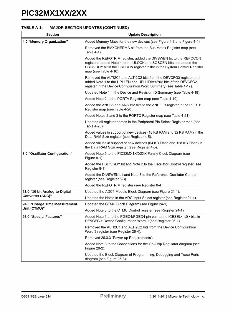
PIC32MX1XX/2XX
4.0 “Memory Organization” Added Memory Maps for the new devices (see Figure 4-3 and Figure 4-4).
Removed the BMXCHEDMA bit from the Bus Matrix Register map (see Table 4-1).
Added the REFOTRIM register, added the DIVSWEN bit to the REFOCON registers, added Note 4 to the ULOCK and SOSCEN bits and added the PBDIVRDY bit in the OSCCON register in the in the System Control Register map (see Table 4-16).
Removed the ALTI2C1 and ALTI2C2 bits from the DEVCFG3 register and added Note 1 to the UPLLEN and UPLLIDIV<2:0> bits of the DEVCFG2 register in the Device Configuration Word Summary (see Table 4-17).
Updated Note 1 in the Device and Revision ID Summary (see Table 4-18).
Added Note 2 to the PORTA Register map (see Table 4-19).
Added the ANSB6 and ANSB12 bits to the ANSELB register in the PORTB Register map (see Table 4-20).
Added Notes 2 and 3 to the PORTC Register map (see Table 4-21).
Updated all register names in the Peripheral Pin Select Register map (see Table 4-23).
Added values in support of new devices (16 KB RAM and 32 KB RAM) in the Data RAM Size register (see Register 4-5).
Added values in support of new devices (64 KB Flash and 128 KB Flash) in the Data RAM Size register (see Register 4-5).
8.0 “Oscillator Configuration” Added Note 5 to the PIC32MX1XX/2XX Family Clock Diagram (see Figure 8-1).
Added the PBDIVRDY bit and Note 2 to the Oscillator Control register (see Register 8-1).
Added the DIVSWEN bit and Note 3 to the Reference Oscillator Control register (see Register 8-3).
Added the REFOTRIM register (see Register 8-4).
21.0 “10-bit Analog-to-Digital Converter (ADC)”
Updated the ADC1 Module Block Diagram (see Figure 21-1).
Updated the Notes in the ADC Input Select register (see Register 21-4).
24.0 “Charge Time Measurement Unit (CTMU)”
Updated the CTMU Block Diagram (see Figure 24-1).
Added Note 3 to the CTMU Control register (see Register 24-1)
26.0 “Special Features” Added Note 1 and the PGEC4/PGED4 pin pair to the ICESEL<1:0> bits in DEVCFG0: Device Configuration Word 0 (see Register 26-1).
Removed the ALTI2C1 and ALTI2C2 bits from the Device Configuration Word 3 register (see Register 26-4).
Removed 26.3.3 “Power-up Requirements”.
Added Note 3 to the Connections for the On-Chip Regulator diagram (see Figure 26-2).
Updated the Block Diagram of Programming, Debugging and Trace Ports diagram (see Figure 26-3).
TABLE A-1: MAJOR SECTION UPDATES (CONTINUED)
Section Update Description
DS61168E-page 314 Preliminary 2011-2012 Microchip Technology Inc.
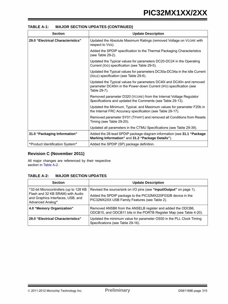
PIC32MX1XX/2XX
Revision C (November 2011)
All major changes are referenced by their respectivesection in Table A-2.
29.0 “Electrical Characteristics” Updated the Absolute Maximum Ratings (removed Voltage on VCORE with respect to VSS).
Added the SPDIP specification to the Thermal Packaging Characteristics (see Table 29-2).
Updated the Typical values for parameters DC20-DC24 in the Operating Current (IDD) specification (see Table 29-5).
Updated the Typical values for parameters DC30a-DC34a in the Idle Current (IIDLE) specification (see Table 29-6).
Updated the Typical values for parameters DC40i and DC40n and removed parameter DC40m in the Power-down Current (IPD) specification (see Table 29-7).
Removed parameter D320 (VCORE) from the Internal Voltage Regulator Specifications and updated the Comments (see Table 29-13).
Updated the Minimum, Typical, and Maximum values for parameter F20b in the Internal FRC Accuracy specification (see Table 29-17).
Removed parameter SY01 (TPWRT) and removed all Conditions from Resets Timing (see Table 29-20).
Updated all parameters in the CTMU Specifications (see Table 29-39).
31.0 “Packaging Information” Added the 28-lead SPDIP package diagram information (see 31.1 “Package Marking Information” and 31.2 “Package Details”).
“Product Identification System” Added the SPDIP (SP) package definition.
TABLE A-1: MAJOR SECTION UPDATES (CONTINUED)
Section Update Description
TABLE A-2: MAJOR SECTION UPDATES
Section Update Description
“32-bit Microcontrollers (up to 128 KB Flash and 32 KB SRAM) with Audio and Graphics Interfaces, USB, and Advanced Analog”
Revised the source/sink on I/O pins (see “Input/Output” on page 1).
Added the SPDIP package to the PIC32MX220F032B device in the PIC32MX2XX USB Family Features (see Table 2).
4.0 “Memory Organization” Removed ANSB6 from the ANSELB register and added the ODCB6, ODCB10, and ODCB11 bits in the PORTB Register Map (see Table 4-20).
29.0 “Electrical Characteristics” Updated the minimum value for parameter OS50 in the PLL Clock Timing Specifications (see Table 29-16).
2011-2012 Microchip Technology Inc. Preliminary DS61168E-page 315
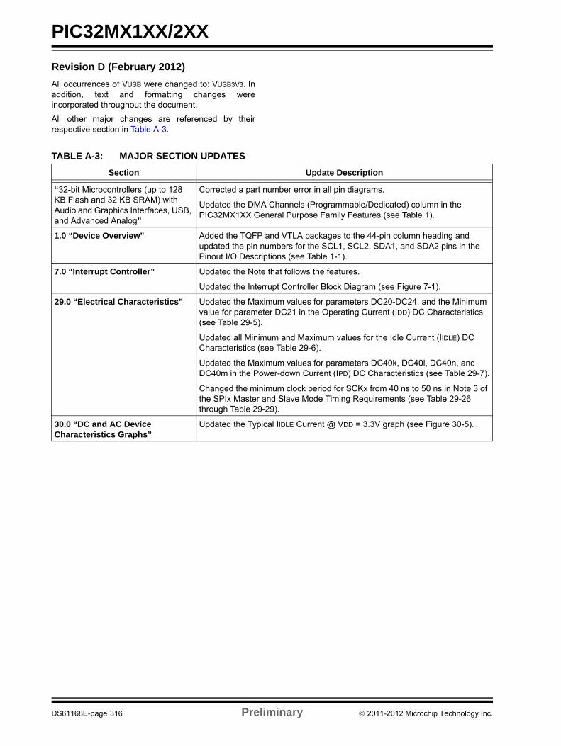
PIC32MX1XX/2XX
Revision D (February 2012)
All occurrences of VUSB were changed to: VUSB3V3. Inaddition, text and formatting changes wereincorporated throughout the document.
All other major changes are referenced by theirrespective section in Table A-3.
TABLE A-3: MAJOR SECTION UPDATES
Section Update Description
“32-bit Microcontrollers (up to 128 KB Flash and 32 KB SRAM) with Audio and Graphics Interfaces, USB, and Advanced Analog”
Corrected a part number error in all pin diagrams.
Updated the DMA Channels (Programmable/Dedicated) column in the PIC32MX1XX General Purpose Family Features (see Table 1).
1.0 “Device Overview” Added the TQFP and VTLA packages to the 44-pin column heading and updated the pin numbers for the SCL1, SCL2, SDA1, and SDA2 pins in the Pinout I/O Descriptions (see Table 1-1).
7.0 “Interrupt Controller” Updated the Note that follows the features.
Updated the Interrupt Controller Block Diagram (see Figure 7-1).
29.0 “Electrical Characteristics” Updated the Maximum values for parameters DC20-DC24, and the Minimum value for parameter DC21 in the Operating Current (IDD) DC Characteristics (see Table 29-5).
Updated all Minimum and Maximum values for the Idle Current (IIDLE) DC Characteristics (see Table 29-6).
Updated the Maximum values for parameters DC40k, DC40l, DC40n, and DC40m in the Power-down Current (IPD) DC Characteristics (see Table 29-7).
Changed the minimum clock period for SCKx from 40 ns to 50 ns in Note 3 of the SPIx Master and Slave Mode Timing Requirements (see Table 29-26 through Table 29-29).
30.0 “DC and AC Device Characteristics Graphs”
Updated the Typical IIDLE Current @ VDD = 3.3V graph (see Figure 30-5).
DS61168E-page 316 Preliminary 2011-2012 Microchip Technology Inc.
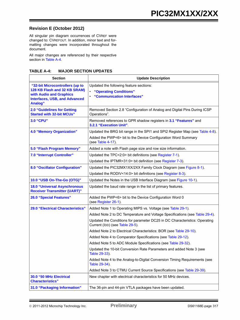
PIC32MX1XX/2XX
Revision E (October 2012)
All singular pin diagram occurrences of CVREF werechanged to: CVREFOUT. In addition, minor text and for-matting changes were incorporated throughout thedocument.
All major changes are referenced by their respectivesection in Table A-4.
TABLE A-4: MAJOR SECTION UPDATES
Section Update Description
“32-bit Microcontrollers (up to 128 KB Flash and 32 KB SRAM) with Audio and Graphics Interfaces, USB, and Advanced Analog”
Updated the following feature sections:
• “Operating Conditions”• “Communication Interfaces”
2.0 “Guidelines for Getting Started with 32-bit MCUs”
Removed Section 2.8 “Configuration of Analog and Digital Pins During ICSP Operations”.
3.0 “CPU” Removed references to GPR shadow registers in 3.1 “Features” and 3.2.1 “Execution Unit”.
4.0 “Memory Organization” Updated the BRG bit range in the SPI1 and SPI2 Register Map (see Table 4-8).
Added the PWP<6> bit to the Device Configuration Word Summary (see Table 4-17).
5.0 “Flash Program Memory” Added a note with Flash page size and row size information.
7.0 “Interrupt Controller” Updated the TPC<2:0> bit definitions (see Register 7-1).
Updated the IPTMR<31:0> bit definition (see Register 7-3).
8.0 “Oscillator Configuration” Updated the PIC32MX1XX/2XX Family Clock Diagram (see Figure 8-1).
Updated the RODIV<14:0> bit definitions (see Register 8-3).
10.0 “USB On-The-Go (OTG)” Updated the Notes in the USB Interface Diagram (see Figure 10-1).
18.0 “Universal Asynchronous Receiver Transmitter (UART)”
Updated the baud rate range in the list of primary features.
26.0 “Special Features” Added the PWP<6> bit to the Device Configuration Word 0 (see Register 26-1).
29.0 “Electrical Characteristics” Added Note 1 to Operating MIPS vs. Voltage (see Table 29-1).
Added Note 2 to DC Temperature and Voltage Specifications (see Table 29-4).
Updated the Conditions for parameter DC25 in DC Characteristics: Operating Current (IDD) (see Table 29-5).
Added Note 2 to Electrical Characteristics: BOR (see Table 29-10).
Added Note 4 to Comparator Specifications (see Table 29-12).
Added Note 5 to ADC Module Specifications (see Table 29-32).
Updated the 10-bit Conversion Rate Parameters and added Note 3 (see Table 29-33).
Added Note 4 to the Analog-to-Digital Conversion Timing Requirements (see Table 29-34).
Added Note 3 to CTMU Current Source Specifications (see Table 29-39).
30.0 “50 MHz Electrical Characteristics”
New chapter with electrical characteristics for 50 MHz devices.
31.0 “Packaging Information” The 36-pin and 44-pin VTLA packages have been updated.
2011-2012 Microchip Technology Inc. Preliminary DS61168E-page 317

PIC32MX1XX/2XX
Notes:
DS61168E-page 318 Preliminary 2011-2012 Microchip Technology Inc.
PIC32MX1XX/2XX
INDEX
Numerics50 MHz Electrical Characteristics ..................................... 285
AAC Characteristics ............................................................ 253
10-Bit Conversion Rate Parameters ......................... 275ADC Specifications ................................................... 273Analog-to-Digital Conversion Requirements............. 276EJTAG Timing Requirements ................................... 284Internal FRC Accuracy.............................................. 255Internal RC Accuracy ................................................ 255OTG Electrical Specifications ................................... 282Parallel Master Port Read Requirements ................. 281Parallel Master Port Write ......................................... 282Parallel Master Port Write Requirements.................. 282Parallel Slave Port Requirements ............................. 280PLL Clock Timing...................................................... 255
Analog-to-Digital Converter (ADC).................................... 201Assembler
MPASM Assembler................................................... 240
BBlock Diagrams
ADC Module.............................................................. 201Comparator I/O Operating Modes............................. 209Comparator Voltage Reference ................................ 213Connections for On-Chip Voltage Regulator............. 235Core and Peripheral Modules ..................................... 19CPU ............................................................................ 31CTMU Configurations
Time Measurement........................................... 215DMA.......................................................................... 103I2C Circuit ................................................................. 172Input Capture ............................................................ 157Interrupt Controller ...................................................... 85JTAG Programming, Debugging and Trace Ports .... 235Output Compare Module........................................... 161PMP Pinout and Connections to External Devices ... 183Reset System.............................................................. 81RTCC........................................................................ 191SPI Module ............................................................... 163Timer1....................................................................... 149Timer2/3/4/5 (16-Bit) ................................................. 153Typical Multiplexed Port Structure ............................ 141UART ........................................................................ 177WDT and Power-up Timer ........................................ 233
Brown-out Reset (BOR)and On-Chip Voltage Regulator................................ 235
CC Compilers
MPLAB C18 .............................................................. 240Charge Time Measurement Unit. See CTMU.Clock Diagram .................................................................... 94Comparator
Specifications............................................................ 252Comparator Module .......................................................... 209Comparator Voltage Reference (CVref ............................. 213Configuration Bit ............................................................... 223Configuring Analog Port Pins............................................ 142
CPUArchitecture Overview ................................................ 32Coprocessor 0 Registers ............................................ 33Core Exception Types ................................................ 34EJTAG Debug Support............................................... 34Power Management ................................................... 34
CPU Module ................................................................. 27, 31CTMU
Registers .................................................................. 216Customer Change Notification Service............................. 323Customer Notification Service .......................................... 323Customer Support............................................................. 323
DDC and AC Characteristics
Graphs and Tables ................................................... 291DC Characteristics............................................................ 244
I/O Pin Input Specifications ...................................... 249I/O Pin Output Specifications.................................... 250Idle Current (IIDLE) .................................................... 247Power-Down Current (IPD)........................................ 248Program Memory...................................................... 251Temperature and Voltage Specifications.................. 245
DC Characteristics (50 MHz) ............................................ 286Idle Current (IIDLE) .................................................... 287Power-Down Current (IPD)........................................ 287
Development Support ....................................................... 239Direct Memory Access (DMA) Controller.......................... 103
EElectrical Characteristics .................................................. 243
AC............................................................................. 253Errata.................................................................................. 16External Clock
Timer1 Timing Requirements ................................... 259Timer2, 3, 4, 5 Timing Requirements ....................... 260Timing Requirements ............................................... 254
External Clock (50 MHz)Timing Requirements ............................................... 288
FFlash Program Memory ...................................................... 77
RTSP Operation ......................................................... 77
II/O Ports ........................................................................... 141
Parallel I/O (PIO) ...................................................... 142Write/Read Timing.................................................... 142
Input Change Notification ................................................. 142Instruction Set................................................................... 237Inter-Integrated Circuit (I2C .............................................. 171Internal Voltage Reference Specifications........................ 252Internet Address ............................................................... 323Interrupt Controller.............................................................. 85
IRG, Vector and Bit Location ...................................... 86
MMemory Maps
PIC32MX11X/21X Devices......................................... 36PIC32MX12X/22X Devices......................................... 37PIC32MX130/230 Devices ......................................... 38PIC32MX150/250 Devices ......................................... 39
2011-2012 Microchip Technology Inc. Preliminary DS61168E-page 319
PIC32MX1XX/2XX
Memory Organization.......................................................... 35Layout ......................................................................... 35
Microchip Internet Web Site .............................................. 323MPLAB ASM30 Assembler, Linker, Librarian ................... 240MPLAB Integrated Development Environment Software .. 239MPLAB PM3 Device Programmer..................................... 242MPLAB REAL ICE In-Circuit Emulator System................. 241MPLINK Object Linker/MPLIB Object Librarian ................ 240
OOscillator Configuration....................................................... 93Output Compare................................................................ 161
PPackaging ......................................................................... 295
Details ....................................................................... 297Marking ..................................................................... 295
Parallel Master Port (PMP) ............................................... 183PIC32 Family USB Interface Diagram............................... 120Pinout I/O Descriptions (table) ............................................ 20Power-on Reset (POR)
and On-Chip Voltage Regulator ................................ 235Power-Saving Features..................................................... 219
CPU Halted Methods ................................................ 219Operation .................................................................. 219with CPU Running..................................................... 219
RReader Response ............................................................. 324Real-Time Clock and Calendar (RTCC)............................ 191Register Maps ............................................................... 40–68Registers
[pin name]R (Peripheral Pin Select Input)................. 147AD1CHS (ADC Input Select) .................................... 207AD1CON1 (A/D Control 1) ........................................ 199AD1CON1 (ADC Control 1) .............................. 199, 203AD1CON2 (ADC Control 2) ...................................... 205AD1CON3 (ADC Control 3) ...................................... 206AD1CSSL (ADC Input Scan Select) ......................... 208ALRMDATE (Alarm Date Value) ............................... 199ALRMDATECLR (ALRMDATE Clear)....................... 199ALRMDATESET (ALRMDATE Set) .......................... 199ALRMTIME (Alarm Time Value) ............................... 198ALRMTIMECLR (ALRMTIME Clear)......................... 199ALRMTIMEINV (ALRMTIME Invert) ......................... 199ALRMTIMESET (ALRMTIME Set) ............................ 199BMXBOOTSZ (Boot Flash (IFM) Size ........................ 76BMXCON (Bus Matrix Configuration) ......................... 71BMXDKPBA (Data RAM Kernel Program
Base Address) .................................................... 72BMXDRMSZ (Data RAM Size Register) ..................... 75BMXDUDBA (Data RAM User Data Base Address) ... 73BMXDUPBA (Data RAM User Program
Base Address) .................................................... 74BMXPFMSZ (Program Flash (PFM) Size) .................. 76BMXPUPBA (Program Flash (PFM) User Program
Base Address) .................................................... 75CM1CON (Comparator 1 Control) ............................ 210CMSTAT (Comparator Control Register) .................. 211CNCONx (Change Notice Control for PORTx) ......... 148CTMUCON (CTMU Control) ..................................... 216CVRCON (Comparator Voltage Reference Control). 214DCHxCON (DMA Channel ’x’ Control)...................... 109DCHxCPTR (DMA Channel ’x’ Cell Pointer) ............. 116DCHxCSIZ (DMA Channel ’x’ Cell-Size)................... 116DCHxDAT (DMA Channel ’x’ Pattern Data) .............. 117
DCHxDPTR (Channel ’x’ Destination Pointer).......... 115DCHxDSA (DMA Channel ’x’ Destination
Start Address)................................................... 113DCHxDSIZ (DMA Channel ’x’ Destination Size)....... 114DCHxECON (DMA Channel ’x’ Event Control)......... 110DCHxINT (DMA Channel ’x’ Interrupt Control) ......... 111DCHxSPTR (DMA Channel ’x’ Source Pointer)........ 115DCHxSSA (DMA Channel ’x’ Source Start Address) 113DCHxSSIZ (DMA Channel ’x’ Source Size).............. 114DCRCCON (DMA CRC Control)............................... 106DCRCDATA (DMA CRC Data) ................................. 108DCRCXOR (DMA CRCXOR Enable) ....................... 108DEVCFG0 (Device Configuration Word 0................. 224DEVCFG1 (Device Configuration Word 1................. 226DEVCFG2 (Device Configuration Word 2................. 228DEVCFG3 (Device Configuration Word 3................. 230DEVID (Device and Revision ID) .............................. 232DMAADDR (DMA Address) ...................................... 105DMAADDR (DMR Address)...................................... 105DMACON (DMA Controller Control) ......................... 104DMASTAT (DMA Status) .......................................... 105I2CxCON (I2C Control)............................................. 173I2CxSTAT (I2C Status) ............................................. 175ICxCON (Input Capture ’x’ Control) .......................... 158IFSx (Interrupt Flag Status) ........................................ 90INTCON (Interrupt Control)......................................... 88INTSTAT (Interrupt Status)......................................... 89IPCx (Interrupt Priority Control) .................................. 91NVMADDR (Flash Address) ....................................... 79NVMCON (Programming Control) .............................. 78NVMDATA (Flash Program Data)............................... 80NVMKEY (Programming Unlock)................................ 79NVMSRCADDR (Source Data Address) .................... 80OCxCON (Output Compare ’x’ Control).................... 162OSCCON (Oscillator Control) ..................................... 95PMADDR (Parallel Port Address) ............................. 188PMAEN (Parallel Port Pin Enable)............................ 189PMCON (Parallel Port Control)................................. 184PMMODE (Parallel Port Mode)................................. 186PMSTAT (Parallel Port Status (Slave Modes Only).. 190REFOCON (Reference Oscillator Control) ................. 99REFOTRIM (Reference Oscillator Trim)................... 101RPnR (Peripheral Pin Select Output) ....................... 147RSWRST (Software Reset) ........................................ 83RTCCON (RTC Control) ........................................... 192RTCDATE (RTC Date Value) ................................... 197RTCTIME (RTC Time Value).................................... 196SPIxCON (SPI Control) ............................................ 164SPIxCON2 (SPI Control 2) ....................................... 167SPIxSTAT (SPI Status)............................................. 168T1CON (Type A Timer Control) ................................ 150TPTMR (Temporal Proximity Timer)........................... 89TxCON (Type B Timer Control) ................................ 155U1ADDR (USB Address) .......................................... 134U1BDTP1 (USB BDT Page 1) .................................. 136U1BDTP2 (USB BDT Page 2) .................................. 137U1BDTP3 (USB BDT Page 3) .................................. 137U1CNFG1 (USB Configuration 1)............................. 138U1CON (USB Control).............................................. 132U1EIE (USB Error Interrupt Enable) ......................... 130U1EIR (USB Error Interrupt Status).......................... 128U1EP0-U1EP15 (USB Endpoint Control) ................. 139U1FRMH (USB Frame Number High) ...................... 135U1FRML (USB Frame Number Low)........................ 134U1IE (USB Interrupt Enable) .................................... 127
DS61168E-page 320 Preliminary 2011-2012 Microchip Technology Inc.
PIC32MX1XX/2XX
U1IR (USB Interrupt)................................................. 126U1OTGCON (USB OTG Control) ............................. 124U1OTGIE (USB OTG Interrupt Enable) .................... 122U1OTGIR (USB OTG Interrupt Status)..................... 121U1OTGSTAT (USB OTG Status).............................. 123U1PWRC (USB Power Control)................................ 125U1SOF (USB SOF Threshold).................................. 136U1STAT (USB Status) .............................................. 131U1TOK (USB Token) ................................................ 135WDTCON (Watchdog Timer Control) ....................... 234
Resets................................................................................. 81Revision History ................................................................ 313RTCALRM (RTC ALARM Control) .................................... 194
SSerial Peripheral Interface (SPI) ....................................... 163Software Simulator (MPLAB SIM)..................................... 241Special Features ............................................................... 223
TTimer1 Module .................................................................. 149Timer2/3, Timer4/5 Modules ............................................. 153Timing Diagrams
10-Bit Analog-to-Digital Conversion (ASAM = 0, SSRC<2:0> = 000) ........................ 277
10-Bit Analog-to-Digital Conversion (ASAM = 1, SS-RC<2:0> = 111, SAMC<4:0> = 00001) ............ 278
EJTAG ...................................................................... 284External Clock........................................................... 253I/O Characteristics .................................................... 256I2Cx Bus Data (Master Mode) .................................. 267I2Cx Bus Data (Slave Mode) .................................... 270I2Cx Bus Start/Stop Bits (Master Mode) ................... 267I2Cx Bus Start/Stop Bits (Slave Mode) ..................... 270Input Capture (CAPx)................................................ 260OCx/PWM................................................................. 261Output Compare (OCx)............................................. 261Parallel Master Port Read......................................... 280Parallel Master Port Write ......................................... 281Parallel Slave Port .................................................... 279SPIx Master Mode (CKE = 0) ................................... 262SPIx Master Mode (CKE = 1) ................................... 263SPIx Slave Mode (CKE = 0) ..................................... 264SPIx Slave Mode (CKE = 1) ..................................... 265Timer1, 2, 3, 4, 5 External Clock............................... 259UART Reception ....................................................... 182UART Transmission (8-bit or 9-bit Data)................... 182
Timing RequirementsCLKO and I/O ........................................................... 256
Timing SpecificationsI2Cx Bus Data Requirements (Master Mode)........... 268I2Cx Bus Data Requirements (Slave Mode)............. 271Input Capture Requirements .................................... 260Output Compare Requirements................................ 261Simple OCx/PWM Mode Requirements ................... 261SPIx Master Mode (CKE = 0) Requirements............ 262SPIx Master Mode (CKE = 1) Requirements............ 263SPIx Slave Mode (CKE = 1) Requirements.............. 265SPIx Slave Mode Requirements (CKE = 0).............. 264
Timing Specifications (50 MHz)SPIx Master Mode (CKE = 0) Requirements............ 288SPIx Master Mode (CKE = 1) Requirements............ 288SPIx Slave Mode (CKE = 1) Requirements.............. 289SPIx Slave Mode Requirements (CKE = 0).............. 289
UUART................................................................................ 177USB On-The-Go (OTG).................................................... 119
VVCAP pin............................................................................ 235Voltage Regulator (On-Chip) ............................................ 235
WWatchdog Timer (WDT).................................................... 233WWW Address ................................................................. 323WWW, On-Line Support ..................................................... 16
2011-2012 Microchip Technology Inc. Preliminary DS61168E-page 321

PIC32MX1XX/2XX
NOTES:
DS61168E-page 322 Preliminary 2011-2012 Microchip Technology Inc.
PIC32MX1XX/2XX
THE MICROCHIP WEB SITE
Microchip provides online support via our WWW site atwww.microchip.com. This web site is used as a meansto make files and information easily available tocustomers. Accessible by using your favorite Internetbrowser, the web site contains the followinginformation:
• Product Support – Data sheets and errata, application notes and sample programs, design resources, user’s guides and hardware support documents, latest software releases and archived software
• General Technical Support – Frequently Asked Questions (FAQs), technical support requests, online discussion groups, Microchip consultant program member listing
• Business of Microchip – Product selector and ordering guides, latest Microchip press releases, listing of seminars and events, listings of Microchip sales offices, distributors and factory representatives
CUSTOMER CHANGE NOTIFICATION SERVICE
Microchip’s customer notification service helps keepcustomers current on Microchip products. Subscriberswill receive e-mail notification whenever there arechanges, updates, revisions or errata related to aspecified product family or development tool of interest.
To register, access the Microchip web site atwww.microchip.com. Under “Support”, click on“Customer Change Notification” and follow theregistration instructions.
CUSTOMER SUPPORT
Users of Microchip products can receive assistancethrough several channels:
• Distributor or Representative
• Local Sales Office
• Field Application Engineer (FAE)
• Technical Support
• Development Systems Information Line
Customers should contact their distributor,representative or field application engineer (FAE) forsupport. Local sales offices are also available to helpcustomers. A listing of sales offices and locations isincluded in the back of this document.
Technical support is available through the web siteat: http://microchip.com/support
2011-2012 Microchip Technology Inc. Preliminary DS61168E-page 323

PIC32MX1XX/2XX
READER RESPONSE
It is our intention to provide you with the best documentation possible to ensure successful use of your Microchipproduct. If you wish to provide your comments on organization, clarity, subject matter, and ways in which ourdocumentation can better serve you, please FAX your comments to the Technical Publications Manager at(480) 792-4150.
Please list the following information, and use this outline to provide us with your comments about this document.
TO: Technical Publications Manager
RE: Reader ResponseTotal Pages Sent ________
From: Name
Company
Address
City / State / ZIP / Country
Telephone: (_______) _________ - _________
Application (optional):
Would you like a reply? Y N
Device: Literature Number:
Questions:
FAX: (______) _________ - _________
DS61168EPIC32MX1XX/2XX
1. What are the best features of this document?
2. How does this document meet your hardware and software development needs?
3. Do you find the organization of this document easy to follow? If not, why?
4. What additions to the document do you think would enhance the structure and subject?
5. What deletions from the document could be made without affecting the overall usefulness?
6. Is there any incorrect or misleading information (what and where)?
7. How would you improve this document?
DS61168E-page 324 Preliminary 2011-2012 Microchip Technology Inc.
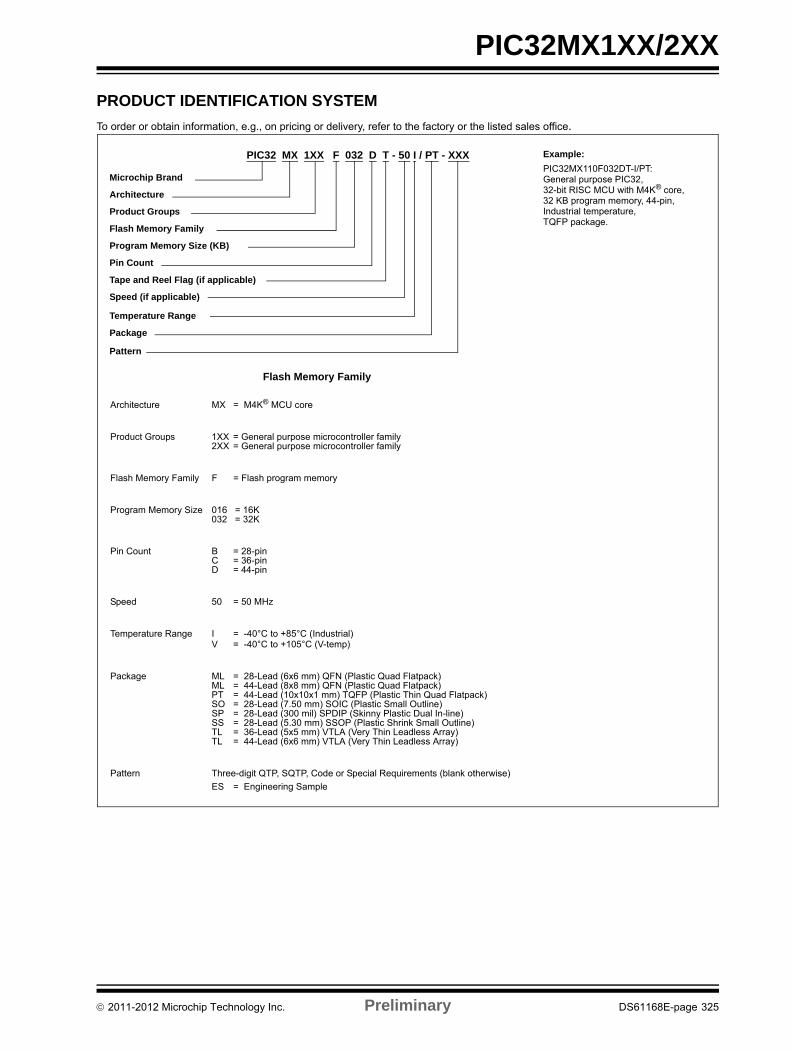
PIC32MX1XX/2XX
PRODUCT IDENTIFICATION SYSTEM
To order or obtain information, e.g., on pricing or delivery, refer to the factory or the listed sales office.
Architecture MX = M4K® MCU core
Product Groups 1XX = General purpose microcontroller family2XX = General purpose microcontroller family
Flash Memory Family F = Flash program memory
Program Memory Size 016 = 16K032 = 32K
Pin Count B = 28-pinC = 36-pinD = 44-pin
Speed 50 = 50 MHz
Temperature Range I = -40°C to +85°C (Industrial)V = -40°C to +105°C (V-temp)
Package ML = 28-Lead (6x6 mm) QFN (Plastic Quad Flatpack)ML = 44-Lead (8x8 mm) QFN (Plastic Quad Flatpack)PT = 44-Lead (10x10x1 mm) TQFP (Plastic Thin Quad Flatpack) SO = 28-Lead (7.50 mm) SOIC (Plastic Small Outline)SP = 28-Lead (300 mil) SPDIP (Skinny Plastic Dual In-line)SS = 28-Lead (5.30 mm) SSOP (Plastic Shrink Small Outline) TL = 36-Lead (5x5 mm) VTLA (Very Thin Leadless Array) TL = 44-Lead (6x6 mm) VTLA (Very Thin Leadless Array)
Pattern Three-digit QTP, SQTP, Code or Special Requirements (blank otherwise)
ES = Engineering Sample
Example:
PIC32MX110F032DT-I/PT:General purpose PIC32, 32-bit RISC MCU with M4K® core,32 KB program memory, 44-pin, Industrial temperature,TQFP package.
Microchip Brand
Architecture
Flash Memory Family
Pin Count
Product Groups
Program Memory Size (KB)
PIC32 MX 1XX F 032 D T - 50 I / PT - XXX
Flash Memory Family
Pattern
Package
Temperature Range
Tape and Reel Flag (if applicable)
Speed (if applicable)
2011-2012 Microchip Technology Inc. Preliminary DS61168E-page 325
PIC32MX1XX/2XX
NOTES:
DS61168E-page 326 Preliminary 2011-2012 Microchip Technology Inc.
Note the following details of the code protection feature on Microchip devices:
• Microchip products meet the specification contained in their particular Microchip Data Sheet.
• Microchip believes that its family of products is one of the most secure families of its kind on the market today, when used in the intended manner and under normal conditions.
• There are dishonest and possibly illegal methods used to breach the code protection feature. All of these methods, to our knowledge, require using the Microchip products in a manner outside the operating specifications contained in Microchip’s Data Sheets. Most likely, the person doing so is engaged in theft of intellectual property.
• Microchip is willing to work with the customer who is concerned about the integrity of their code.
• Neither Microchip nor any other semiconductor manufacturer can guarantee the security of their code. Code protection does not mean that we are guaranteeing the product as “unbreakable.”
Code protection is constantly evolving. We at Microchip are committed to continuously improving the code protection features of ourproducts. Attempts to break Microchip’s code protection feature may be a violation of the Digital Millennium Copyright Act. If such actsallow unauthorized access to your software or other copyrighted work, you may have a right to sue for relief under that Act.
Information contained in this publication regarding deviceapplications and the like is provided only for your convenienceand may be superseded by updates. It is your responsibility toensure that your application meets with your specifications.MICROCHIP MAKES NO REPRESENTATIONS ORWARRANTIES OF ANY KIND WHETHER EXPRESS ORIMPLIED, WRITTEN OR ORAL, STATUTORY OROTHERWISE, RELATED TO THE INFORMATION,INCLUDING BUT NOT LIMITED TO ITS CONDITION,QUALITY, PERFORMANCE, MERCHANTABILITY ORFITNESS FOR PURPOSE. Microchip disclaims all liabilityarising from this information and its use. Use of Microchipdevices in life support and/or safety applications is entirely atthe buyer’s risk, and the buyer agrees to defend, indemnify andhold harmless Microchip from any and all damages, claims,suits, or expenses resulting from such use. No licenses areconveyed, implicitly or otherwise, under any Microchipintellectual property rights.
2011-2012 Microchip Technology Inc. Prelimin
QUALITY MANAGEMENT SYSTEM CERTIFIED BY DNV
== ISO/TS 16949 ==
Trademarks
The Microchip name and logo, the Microchip logo, dsPIC, FlashFlex, KEELOQ, KEELOQ logo, MPLAB, PIC, PICmicro, PICSTART, PIC32 logo, rfPIC, SST, SST Logo, SuperFlash and UNI/O are registered trademarks of Microchip Technology Incorporated in the U.S.A. and other countries.
FilterLab, Hampshire, HI-TECH C, Linear Active Thermistor, MTP, SEEVAL and The Embedded Control Solutions Company are registered trademarks of Microchip Technology Incorporated in the U.S.A.
Silicon Storage Technology is a registered trademark of Microchip Technology Inc. in other countries.
Analog-for-the-Digital Age, Application Maestro, BodyCom, chipKIT, chipKIT logo, CodeGuard, dsPICDEM, dsPICDEM.net, dsPICworks, dsSPEAK, ECAN, ECONOMONITOR, FanSense, HI-TIDE, In-Circuit Serial Programming, ICSP, Mindi, MiWi, MPASM, MPF, MPLAB Certified logo, MPLIB, MPLINK, mTouch, Omniscient Code Generation, PICC, PICC-18, PICDEM, PICDEM.net, PICkit, PICtail, REAL ICE, rfLAB, Select Mode, SQI, Serial Quad I/O, Total Endurance, TSHARC, UniWinDriver, WiperLock, ZENA and Z-Scale are trademarks of Microchip Technology Incorporated in the U.S.A. and other countries.
SQTP is a service mark of Microchip Technology Incorporated in the U.S.A.
GestIC and ULPP are registered trademarks of Microchip Technology Germany II GmbH & Co. & KG, a subsidiary of Microchip Technology Inc., in other countries.
All other trademarks mentioned herein are property of their respective companies.
© 2011-2012, Microchip Technology Incorporated, Printed in the U.S.A., All Rights Reserved.
Printed on recycled paper.
ISBN: 978-1-62076-640-8
Microchip received ISO/TS-16949:2009 certification for its worldwide
ary DS61168E-page 327
headquarters, design and wafer fabrication facilities in Chandler and Tempe, Arizona; Gresham, Oregon and design centers in California and India. The Company’s quality system processes and procedures are for its PIC® MCUs and dsPIC® DSCs, KEELOQ® code hopping devices, Serial EEPROMs, microperipherals, nonvolatile memory and analog products. In addition, Microchip’s quality system for the design and manufacture of development systems is ISO 9001:2000 certified.

DS61168E-page 328 Preliminary 2011-2012 Microchip Technology Inc.
AMERICASCorporate Office2355 West Chandler Blvd.Chandler, AZ 85224-6199Tel: 480-792-7200 Fax: 480-792-7277Technical Support: http://www.microchip.com/supportWeb Address: www.microchip.com
AtlantaDuluth, GA Tel: 678-957-9614 Fax: 678-957-1455
BostonWestborough, MA Tel: 774-760-0087 Fax: 774-760-0088
ChicagoItasca, IL Tel: 630-285-0071 Fax: 630-285-0075
ClevelandIndependence, OH Tel: 216-447-0464 Fax: 216-447-0643
DallasAddison, TX Tel: 972-818-7423 Fax: 972-818-2924
DetroitFarmington Hills, MI Tel: 248-538-2250Fax: 248-538-2260
IndianapolisNoblesville, IN Tel: 317-773-8323Fax: 317-773-5453
Los AngelesMission Viejo, CA Tel: 949-462-9523 Fax: 949-462-9608
Santa ClaraSanta Clara, CA Tel: 408-961-6444Fax: 408-961-6445
TorontoMississauga, Ontario, CanadaTel: 905-673-0699 Fax: 905-673-6509
ASIA/PACIFICAsia Pacific OfficeSuites 3707-14, 37th FloorTower 6, The GatewayHarbour City, KowloonHong KongTel: 852-2401-1200Fax: 852-2401-3431
Australia - SydneyTel: 61-2-9868-6733Fax: 61-2-9868-6755
China - BeijingTel: 86-10-8569-7000 Fax: 86-10-8528-2104
China - ChengduTel: 86-28-8665-5511Fax: 86-28-8665-7889
China - ChongqingTel: 86-23-8980-9588Fax: 86-23-8980-9500
China - HangzhouTel: 86-571-2819-3187 Fax: 86-571-2819-3189
China - Hong Kong SARTel: 852-2401-1200 Fax: 852-2401-3431
China - NanjingTel: 86-25-8473-2460Fax: 86-25-8473-2470
China - QingdaoTel: 86-532-8502-7355Fax: 86-532-8502-7205
China - ShanghaiTel: 86-21-5407-5533 Fax: 86-21-5407-5066
China - ShenyangTel: 86-24-2334-2829Fax: 86-24-2334-2393
China - ShenzhenTel: 86-755-8203-2660 Fax: 86-755-8203-1760
China - WuhanTel: 86-27-5980-5300Fax: 86-27-5980-5118
China - XianTel: 86-29-8833-7252Fax: 86-29-8833-7256
China - XiamenTel: 86-592-2388138 Fax: 86-592-2388130
China - ZhuhaiTel: 86-756-3210040 Fax: 86-756-3210049
ASIA/PACIFICIndia - BangaloreTel: 91-80-3090-4444 Fax: 91-80-3090-4123
India - New DelhiTel: 91-11-4160-8631Fax: 91-11-4160-8632
India - PuneTel: 91-20-2566-1512Fax: 91-20-2566-1513
Japan - OsakaTel: 81-66-152-7160 Fax: 81-66-152-9310
Japan - YokohamaTel: 81-45-471- 6166 Fax: 81-45-471-6122
Korea - DaeguTel: 82-53-744-4301Fax: 82-53-744-4302
Korea - SeoulTel: 82-2-554-7200Fax: 82-2-558-5932 or 82-2-558-5934
Malaysia - Kuala LumpurTel: 60-3-6201-9857Fax: 60-3-6201-9859
Malaysia - PenangTel: 60-4-227-8870Fax: 60-4-227-4068
Philippines - ManilaTel: 63-2-634-9065Fax: 63-2-634-9069
SingaporeTel: 65-6334-8870Fax: 65-6334-8850
Taiwan - Hsin ChuTel: 886-3-5778-366Fax: 886-3-5770-955
Taiwan - KaohsiungTel: 886-7-536-4818Fax: 886-7-330-9305
Taiwan - TaipeiTel: 886-2-2500-6610 Fax: 886-2-2508-0102
Thailand - BangkokTel: 66-2-694-1351Fax: 66-2-694-1350
EUROPEAustria - WelsTel: 43-7242-2244-39Fax: 43-7242-2244-393Denmark - CopenhagenTel: 45-4450-2828 Fax: 45-4485-2829
France - ParisTel: 33-1-69-53-63-20 Fax: 33-1-69-30-90-79
Germany - MunichTel: 49-89-627-144-0 Fax: 49-89-627-144-44
Italy - Milan Tel: 39-0331-742611 Fax: 39-0331-466781
Netherlands - DrunenTel: 31-416-690399 Fax: 31-416-690340
Spain - MadridTel: 34-91-708-08-90Fax: 34-91-708-08-91
UK - WokinghamTel: 44-118-921-5869Fax: 44-118-921-5820
Worldwide Sales and Service
11/29/11


![32V Dual Microstepping Motor Driver IC with SPI...SDO OE12,OE34 CK, [AP1021] 015000428-J-00 2015/01 - 4 - 5. オーダリングガイド AP1021AEN -40~85 C 32-pin QFN EN 6. ピン配置と機能説明](https://img.pdfslide.tips/doc/110x75/6083d403b86ebf65751a73c9/32v-dual-microstepping-motor-driver-ic-with-spi-sdo-oe12oe34-ck-ap1021-015000428-j-00.jpg)