Embed Size (px)
Citation preview

POSTER PRESENTATION

2017
3rd AnnualInnovations in Large-Area Electronics ConferencePOSTER PRESENTATION
1: Organic Synergisms: Eumelanin/PEDOT(PSS) integration for ITO-free electrodes in bioelectronics and nanomedicine
Ludovico Migliaccio,1,2 Salvatore Aprano,1 Luca Iannuzzi,1 Maria Grazia Maglione,1 Paolo Tassini,1Carla Minarini,1 Paola Manini,2 Alessandro Pezzella2 1 ENEA Agenzia Nazionale per Le Nuove Tecnologie lEnergia e lo Sviluppo Economico Sostenibile, SSPT-PROMAS-NANO, C.R.Portici, Portici, NA, Italy 2 Università degli Studi di Napoli Federico II - Department of Chemical Sciences, Via Cintia n.4, Napoli, Italy
ABSTRACT
Organic Bioelectronics applications are largely dictated by the chemical nature of the materials that transduce signals across the biotic/abiotic interfaces1. Among the available materials for functional biocompatible interfaces, the human pigment eumelanin is currently gaining increasing interest.This black insoluble pigment of human skin, hair, eyes and nigral neurons (neuromelanin),2 featuring unique assortment of chemical physical properties3,arises biogenetically from the aminoacid tyrosine via the oxidative polymerization of 5,6-dihydroxyindole (DHI) and/or 5,6-dihydroxyindole-2-carboxylic acid (DHICA)2,3. Two main obstacles hampered a full exploitation of eumelanin based devices: (i) the actual eumelanin insolubility in any solvents, preventing easy processability of the pigment as well as the devices fabrication; (ii) its low conductivity, limiting both the range of possible working potential and functional applications.To improve the electrical performances of the eumelanin thin films, a clear-cut approach lies in the hybridization with a suitable conductive counterpart. In this view, π-conjugated molecules featuring conductive pathways appear a key choice in the production of new organic materials for electronic (nano)devices.
Here, we present the first (at the best of our knowledge) preparation of an eumelanin-PEDOT blend, featuring valuable functional and processing properties, like easy films preparation, high adhesion, good electrical conductivity and biocompatibility. The hybrid was characterized by chemical, physical, electrical and morphological analysis.The biocompatibility and toxicity was investigated in view of its potential exploitation as bio-interface material.
1. Berggren M., and Richter-Dahlfors A. (2007). Adv Mater, Vol.19, p.3201-3213.
2. d’Ischia M., Wakamatsu K., Napolitano A., Briganti S., Garcia-Borron J. C.et al. (2013). Pigmentcell& melanoma research, Vol.26, p.616-633.
3. d’Ischia M., Napolitano A., Pezzella A., Meredith P. and Sarna T. (2009).AngewChemIntEdit,Vol.48, p.3914-3921.
BIOGRAPHY
Alessandro Pezzella received his Ph.D. in Chemistry in 1997. He has carried out research mainly in the field of 5,6-dihydroxyindole polymerization, melanin pigment characterization, and oxidative behavior of phenolic compounds. More recently, his interest is focusing on the applications of bioinspired polymers (melanins and eumelanins)in organic electronics and bioelectronics. His research activity has produced some 100 publications including international and national patents, research papers, reviews, and book chapters.
1
2017
3rd AnnualInnovations in Large-Area Electronics Conference POSTER PRESENTATION
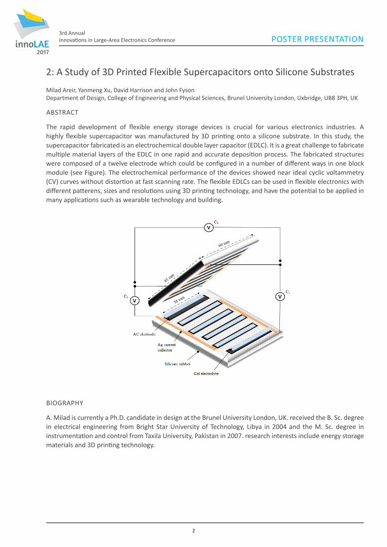
2: A Study of 3D Printed Flexible Supercapacitors onto Silicone Substrates
Milad Areir, Yanmeng Xu, David Harrison and John Fyson Department of Design, College of Engineering and Physical Sciences, Brunel University London, Uxbridge, UB8 3PH, UK
ABSTRACT
The rapid development of flexible energy storage devices is crucial for various electronics industries. A highly flexible supercapacitor was manufactured by 3D printing onto a silicone substrate. In this study, the supercapacitor fabricated is an electrochemical double layer capacitor (EDLC). It is a great challenge to fabricate multiple material layers of the EDLC in one rapid and accurate deposition process. The fabricated structures were composed of a twelve electrode which could be configured in a number of different ways in one block module (see Figure). The electrochemical performance of the devices showed near ideal cyclic voltammetry (CV) curves without distortion at fast scanning rate. The flexible EDLCs can be used in flexible electronics with different patterens, sizes and resolutions using 3D printing technology, and have the potential to be applied in many applications such as wearable technology and building.
BIOGRAPHY
A. Milad is currently a Ph.D. candidate in design at the Brunel University London, UK. received the B. Sc. degree in electrical engineering from Bright Star University of Technology, Libya in 2004 and the M. Sc. degree in instrumentation and control from Taxila University, Pakistan in 2007. research interests include energy storage materials and 3D printing technology.
2

2017
3rd AnnualInnovations in Large-Area Electronics ConferenceSESSION 4: ENERGY HARVESTING & STORAGE
3: Printed nanowires for applications in magnetoelectric sensors and energy harvesters
Chess Boughey, Michael Smith, Yeonsik Choi & Sohini Kar-Narayan* Department of Materials and Science and Metallurgy, University of Cambridge, UK
ABSTRACT
Aerosol jet printing and template–assisted electrodeposition are both low–temperature, fast, simple and scalable growth techniques which have been used in this work to fabricate a magnetoelectric (ME) composite device with possible future applications as either a sensor or an energy harvester. ME composite devices convert magnetic fields into electrical energy via strain coupling of the ferromagnetic and piezoelectric components i.e. via magnetostriction and the piezoelectric effect. In this work, ferromagnetic nickel nanowires were first grown via electrodeposition within a nanoporous anodized alumina template and subsequently released from the template and dispersed in a solution of the piezoelectric polymer; polyvinylidene fluoride trifluoroethylene (P(VDF-TrFE)). Using this as an ink for aerosol jet printing, one can print a ME film. One device architecture attempted in this work is a fully-printed flexible device where interdigitated electrodes are printed first using a silver nanoparticle ink on a plastic substrate followed by deposition of the NW dispersion on top using the same printing process, see figure 1. After annealing and poling steps, the ME device has the potential to be tested as either a magnetic field sensor or a vibrational / magnetic energy harvesting device or both.
Aerosol jet printing is a relatively new deposition technique compared to other printing technologies where an aerosol of an ink is generated and a sheath gas is used to focus a jet of the ink onto a substrate. The advantages of this technique compared to ink-jet printing for example, include a wider range of compatible inks both conductive and dielectric with a wider range of viscosities. It is also possible to print a variety of nanowire-based inks of other materials such as piezoelectric and thermoelectric and carbon nanotubes, amongst others.
Printed nanowires for applications in magnetoelectric sensors and energy harvesters
Chess Boughey, Michael Smith, Yeonsik Choi & Sohini Kar-Narayan*
Department of Materials and Science and Metallurgy, University of Cambridge, UK
Abstract
Aerosol jet printing and template–assisted electrodeposition are both low–temperature, fast, simple and scalable growth techniques which have been used in this work to fabricate a magnetoelectric (ME) composite device with possible future applications as either a sensor or an energy harvester. ME composite devices convert magnetic fields into electrical energy via strain coupling of the ferromagnetic and piezoelectric components i.e. via magnetostriction and the piezoelectric effect. In this work, ferromagnetic nickel nanowires were first grown via electrodeposition within a nanoporous anodized alumina template and subsequently released from the template and dispersed in a solution of the piezoelectric polymer; polyvinylidene fluoride trifluoroethylene (P(VDF-TrFE)). Using this as an ink for aerosol jet printing, one can print a ME film. One device architecture attempted in this work is a fully-printed flexible device where interdigitated electrodes are printed first using a silver nanoparticle ink on a plastic substrate followed by deposition of the NW dispersion on top using the same printing process, see figure 1. After annealing and poling steps, the ME device has the potential to be tested as either a magnetic field sensor or a vibrational / magnetic energy harvesting device or both.
Aerosol jet printing is a relatively new deposition technique compared to other printing technologies where an aerosol of an ink is generated and a sheath gas is used to focus a jet of the ink onto a substrate. The advantages of this technique compared to ink-jet printing for example, include a wider range of compatible inks both conductive and dielectric with a wider range of viscosities. It is also possible to print a variety of nanowire-based inks of other materials such as piezoelectric and thermoelectric and carbon nanotubes, amongst others.
Figure 1: example of a fully printed magnetoelectric device based on a composite ferromagnetic nanowire – piezoelectric polymer based ink.
Figure 1: example of a fully printed magnetoelectric device based on a composite ferromagnetic nanowire – piezoelectric polymer based ink.
BIOGRAPHY
Chess Boughey is a 3rd year PhD student in the Kar-Narayan group in the Department of Materials Science & Metallurgy at the University of Cambridge and his research focuses on electrodeposited nanowires and other scalable fabrication techniques for piezoelectric nanogenerators and magnetoelectric energy harvesters and sensors. He is funded by the nanoscience and nanotechnology centre for doctoral training (EPSRC) as well as benefiting from their supervisor’s ERC starting grant. His undergraduate degree was in physics from Imperial College London where they specialized in gravure printed organic field effect transistors in their final year.
3

2017
3rd AnnualInnovations in Large-Area Electronics Conference POSTER PRESENTATION
4: Control of guided and space waves by meta-surfaces
Luigi La Spada and Yang Hao
ABSTRACT
A huge interest in manipulating waves has grown: the possibility to control electromagnetic waves (in terms of guided propagation and space radiation) is crucial for several application fields [1]. Although the topic has been studied in the past, new research ideas emerged, including the use of meta-surfaces, artificially designed planar materials with sub-wavelength dimensions. The main advantage is the possibility to accurate modify at will: amplitude, phase and polarization of both electric and magnetic field components [2]. Recently, several techniques have been proposed ranging from microwave to optical frequencies [3]: in particular, array of pillars/crossed slit structures [4] metallic patches [5], optical scatters [6], hologram imagers [7], thin films [8] and nanocomposites [9]. All such works aimed to control modes phase and consequently manipulate their propagation, by engineering the dimensions of unit elements within the array. Although all such examples address specific issues, they are restricted to certain geometries and shapes. A more generic approach is still missing. The aim of this work is to present a new design technique for arbitrary meta-surface structures to design devices by linking their geometrical parameters with specific required electromagnetic characteristics. To validate and test the proposed approach, an example for surface wave cloaking is numerically and experimentally reported, (in the frequency range 8-12 GHz) showing good performance in terms of polarization/source independence and broadband behaviour.
REFERENCES
[1] J. A. Polo, T.G. Mackay, A. Lakhtakia, “Electromagnetic Surface Waves: A Modern Perspective”, Elsevier, 2013.
[2] N. Yu and F. Capasso, “Flat optics with designer metasurfaces,” Nature Materials, vol. 13, pp.139-150, 2014.
[3] P. A. Huidobro, M. L. Nesterov, L. Martín-Moreno and F. J. García-Vidal, “Transformation Optics for Plasmonics,” Nano Lett., vol. 10, pp 1985–1990, 2010.
[4] H. Shi, C. Wang, C. Du, X. Luo, X. Dong, and H. Gao, “Beam manipulating by metallic nano-slits with variant widths,” Opt. Express, vol. 13, pp. 6815-6820, 2005.
[5] A.B. Yakovlev, M.G. Silveirinha, O. Luukkonen, C.R. Simovski, I.S. Nefedov, and S.A. Tretyakov, “Characterization of Surface-Wave and Leaky-Wave Propagation on Wire-Medium Slabs and Mushroom Structures Based on Local and Nonlocal Homogenization Models,” IEEE Transactions on Microwave Theory and Techniques, vol.57, pp.2700-2714, 2009.
[6] N. Yu, et al. “A broadband, background-free quarter-wave plate based on plasmonic metasurfaces,” Nano Lett., vol. 12, pp. 6328–6333, 2012.
[7] I. Dolev, , I. Epstein, and A. Arie, “A. Surface-plasmon holographic beam shaping,” Phys. Rev. Lett., vol. 109, 203903, 2012.
[8] H. Dotan, et al. “Resonant light trapping in ultrathin films for water splitting,” Nature Materials, vol. 12, pp. 158–164, 2013.
[9] L. La Spada, T. M. McManus, A. Dyke, S. Haq, L. Zhang, Q. Cheng and Y. Hao, “Surface Wave Cloak from Graded Refractive Index Nanocomposites,” Sci. Rep., 6, 29363, 2016.
Control of guided and space waves by meta-surfaces Luigi La Spada and Yang Hao
A huge interest in manipulating waves has grown: the possibility to control electromagnetic waves (in terms of guided propagation and space radiation) is crucial for several application fields [1]. Although the topic has been studied in the past, new research ideas emerged, including the use of meta-surfaces, artificially designed planar materials with sub-wavelength dimensions. The main advantage is the possibility to accurate modify at will: amplitude, phase and polarization of both electric and magnetic field components [2]. Recently, several techniques have been proposed ranging from microwave to optical frequencies [3]: in particular, array of pillars/crossed slit structures [4] metallic patches [5], optical scatters [6], hologram imagers [7], thin films [8] and nanocomposites [9]. All such works aimed to control modes phase and consequently manipulate their propagation, by engineering the dimensions of unit elements within the array. Although all such examples address specific issues, they are restricted to certain geometries and shapes. A more generic approach is still missing. The aim of this work is to present a new design technique for arbitrary meta-surface structures to design devices by linking their geometrical parameters with specific required electromagnetic characteristics. To validate and test the proposed approach, an example for surface wave cloaking is numerically and experimentally reported, (in the frequency range 8-12 GHz) showing good performance in terms of polarization/source independence and broadband behaviour.
(a) (b)
Fig1: (a) Structure under study and (b) surface wave cloaking device in action REFERENCES [1] J. A. Polo, T.G. Mackay, A. Lakhtakia, "Electromagnetic Surface Waves: A Modern
Perspective", Elsevier, 2013. [2] N. Yu and F. Capasso, “Flat optics with designer metasurfaces,” Nature Materials, vol. 13,
pp.139-150, 2014. [3] P. A. Huidobro, M. L. Nesterov, L. Martín-Moreno and F. J. García-Vidal, “Transformation
Optics for Plasmonics,” Nano Lett., vol. 10, pp 1985–1990, 2010. [4] H. Shi, C. Wang, C. Du, X. Luo, X. Dong, and H. Gao, "Beam manipulating by metallic nano-
slits with variant widths," Opt. Express, vol. 13, pp. 6815-6820, 2005. [5] A.B. Yakovlev, M.G. Silveirinha, O. Luukkonen, C.R. Simovski, I.S. Nefedov, and S.A.
Tretyakov, "Characterization of Surface-Wave and Leaky-Wave Propagation on Wire-Medium Slabs and Mushroom Structures Based on Local and Nonlocal Homogenization Models," IEEE Transactions on Microwave Theory and Techniques, vol.57, pp.2700-2714, 2009.
[6] N. Yu, et al. “A broadband, background-free quarter-wave plate based on plasmonic metasurfaces,” Nano Lett., vol. 12, pp. 6328–6333, 2012.
[7] I. Dolev, , I. Epstein, and A. Arie, “A. Surface-plasmon holographic beam shaping,” Phys. Rev. Lett., vol. 109, 203903, 2012.
[8] H. Dotan, et al. “Resonant light trapping in ultrathin films for water splitting,” Nature Materials, vol. 12, pp. 158–164, 2013.
[9] L. La Spada, T. M. McManus, A. Dyke, S. Haq, L. Zhang, Q. Cheng and Y. Hao, “Surface Wave Cloak from Graded Refractive Index Nanocomposites,” Sci. Rep., 6, 29363, 2016.
4
2017
3rd AnnualInnovations in Large-Area Electronics ConferencePOSTER PRESENTATION
BIOGRAPHIES
Prof. Yang Hao received the Ph.D. degree from the Centre for Communications Research (CCR) at the University of Bristol, U.K. in 1998. From 1998 to 2000, he was a postdoc research fellow at the School of Electrical and Electronic Engineering, University of Birmingham, U.K. In May 2000, he joined the Antenna and Electromagnetics Group, Queen Mary, University of London, London, U.K. first as a lecturer and was promoted to Reader in 2005 and to Professor in 2007.
He currently leads a £4.6M EPSRC QUEST programme grant on transformation electromagnetics and microwave metamaterials. He is a management board member of Cambridge Graphene Center, which has attracted over £25M funding from UK EPSRC. Over the years, he developed several fully-integrated antenna solutions based on novel artificial materials to reduce mutual RF interference, weight, cost and system complexity for security, aerospace and healthcare. He developed, with leading UK industries, novel and emergent gradient index materials to reduce mass, footprint and profile of low frequency and broadband antennas. He also co-developed the first stable active non-Foster’s metamaterial to enhance usability through small antenna size, high directivity, and tuneable operational frequency. He coined the term ‘Body-centric wireless communications’, i.e. networking among wearable and implantable wireless sensors on the human body. He was the first to characterize and include the human body as a communication medium between on-body sensors using surface and creeping waves. He contributed to the industrial development of the first wireless sensors for healthcare monitoring, digital plaster antennas and textile antennas. Professor Hao is a strategic advisory board member for Engineering and Physical Sciences Research Council (EPSRC), where he is committed to championing RF/microwave engineering for reshaping the future of UK manufacturing and electronics.
Dr. Luigi La Spada received his bachelor’s degree, summa cum laude, in Electronics Engineering from the University of Roma Tre, Rome, Italy, in 2008.
In 2010, he received his master’s degree, summa cum laude, in Information and Communication technology from the University of Roma Tre.
From 2011 to 2013, he was with the Department of Applied Electronics, University of Roma Tre, where he worked as a PhD student (scholarship winner) at the Doctoral School in Engineering in the Biomedical Electronics, Electromagnetics, and Telecommunications section. In 2013, he was with the Department of Electrical and Systems Engineering, University of Pennsylvania (Philadelphia, USA), as Visiting Researcher.
In 2014, he received his PhD in Electronic Engineering and from March 2014, he was employed as a Postdoctoral Research Assistant in the School of Electronic Engineering and Computer Science at Queen Mary University of London. Here, he works with Professor Yang Hao in the Antennas and Electromagnetics research group, as part of the QUEST project.
His main research interests are microwave, terahertz, and optical applications of complex media and metamaterials; design of miniaturized sensors and antennas based on metamaterial technology; biological and biomedical applications of plasmonic nanoparticles; analysis and synthesis of planar metamaterials and radiating elements for sensing and telecommunications applications.
5
2017
3rd AnnualInnovations in Large-Area Electronics Conference POSTER PRESENTATION
5: SIMLIFT: Towards single micron LIFT technology
D.Beynon*, B.Clifford*, R.Geremia ^, D.Karnakis^, D.Deganello* * WCPC, Swansea University, Swansea, UK ^ Oxford lasers, Didcot, Oxfordshire, UK
ABSTRACT
Laser Induced Forward Transfer (LIFT) is a key enabling technology for large area processing of printed electronics capable to print a wide range of materials rapidly and digitally. A major barrier for large scale implementation & adoption of the technology is the current achievable printing resolution, commonly reliably limited to the tens of micron. SIMLIFT is an EPSRC CimLAE Pathfinder project aiming to overcome current limits proposing a transformative development of the technology, refining its resolution to a new reliable level towards single micron resolution.
In LIFT, a donor substrate ink carrier is locally irradiated by a short pulse laser causing the transfer of material from the donor layer to a receiving substrate. The donor layer and laser processing are keys for precision patterning. To address the challenge of reliable single micron patterning, SIMLIFT will analyse the effect of varying thin film donor deposition processes (namely spin coating, blade coating, forward roll coating) on the donor film morphology and resulting transfer; it will explore the interaction with varying laser pulse duration that dictates the physical ejection mechanism (namely from nanosecond, picosecond, to femtosecond level duration pulsed lasers). The accuracy of laser processing will be further explored through the novel integration of new microlens arrays for affordable accurate digital patterning.
For the first time influencing parameters will be systematically analysed and compared at a dimensional scale close to that of the laser wavelength; introducing novelty both in donor deposition & laser processing, with the exploration of forward roll coating as a new LAE compatible donor layer deposition method. Gains are expected through the new adoption of microlens arrays for accurate digital patterning by lasers. This research will provide a new insight and scalable technological solutions leading to unique enhancement of the technology to SIMLIFT for large scale adoption of technology for digital processing
The pathfinder project joins together academic and industrial partners to give a unique combination of skills; the project will include the Welsh Centre for Printing and Coating (Swansea University), a leading research centre in printing and printed electronic, with the key partnership and support of Oxford Lasers Ltd, a leading British Industrial laser technology system integrator. The project will also benefit by the support and guidance of a dedicated industrial end-user advisory board.
BIOGRAPHY
Dr. Davide Deganello is an Associate Professor at the College of Engineering, Swansea University, where is deputy director at the Welsh Centre for Printing and Coating (WCPC). His research interests comprise the development of printing technologies and of functional materials for novel applications. For this goal, Davide’s experience covers from large scale roll-to roll printing to one-off additive manufacturing, experience supported by study of material formulation, underlining rheology and CFD modelling. Since his first appointment at Swansea in 2011, Davide has developed a sustained program of research, inclusive of a number of Research Council, collaborative & industrial projects (in collaboration also with EPSRC Centre for Innovative Manufacturing in Large-Area Electronics) targeted to development of novel solutions and materials for energy storage, electronic, smart packaging, and biomedical applications. His research has led, together to a number of publications in high impact international journals, to patents and industrial investments.
6

2017
3rd AnnualInnovations in Large-Area Electronics ConferencePOSTER PRESENTATION
6: Unveiling the potential of adhesion lithography towards development of plastic nanoelectronics
Dimitra G. Georgiadou, James Semple, Gwenhivir Wyatt-Moon and Thomas D. Anthopoulos Physics Department, Imperial College London, London, United Kingdom
ABSTRACT
Adhesion lithography (a-Lith) is a patterning technique that is based on the modification of adhesion forces between two sequentially deposited metals by functionalising the surface of one of them with a suitable self-assembled monolayer (SAM)1. The final a-Lith patterned structure comprises two metals separated laterally by a nanogap of <15 nm (Figure 1). The competitive advantage of this technique is that it is simple and scalable with high throughput, while it can be applied in any type and size of substrates.
Recently, we demonstrated the scalability potential of a-Lith by developing a semi-automated system to perform the peeling of the second metal layer that critically defines the nanogap size and its quality and thus we maximised the process yield. Significant progress has been also achieved in applying a-Lith to plastic (flexible) substrates and different types of metals to create symmetric or asymmetric electrode structures.
The versatility offered by this simple patterning technique to manufacture any type of coplanar metal structures on the same substrate enables the simultaneous fabrication and statistical study of a great number of electronic devices by simply spin-coating the material of choice on top of the metal structures from its solution and applying low temperature thermal annealing to retain compatibility of the whole process with plastic substrates.
Herein, we will describe how deposition of a suitable functional material in the nanogap can give rise to a plethora of high performing nanoelectronic devices, such as radiofrequency Schottky diodes, nanoscale light-emitting diodes, photodetectors and ferroelectric tunnel junction memory devices. Emphasis will be placed on the different requirements posed by each application in terms of materials processing and electrodes geometry. Finally, we will showcase successful examples of proof-of-concept functional devices.
1. Beesley DJ, Semple J, Jagadamma LK, Amassian A, McLachlan MA, Anthopoulos TD, et al. Sub-15-nm patterning of asymmetric metal electrodes and devices by adhesion lithography. Nature Communications 2014, 5.
BIOGRAPHY
Dr Dimitra G. Georgiadou is a Marie Skłodowska-Curie Research Fellow in the Experimental Solid State Physics group (EXSS) at the Blackett Laboratory, Imperial College London. Dimitra received her PhD in Photochemistry/Organic Electronics from the National Technical University of Athens. Before that she obtained a Master’s Degree in Advanced Materials Science from the Technical University of Munich, Ludvig-Maximilians University of Munich and University of Augsburg. She has also gained industrial experience through internships in Procter&Gamble, Italy, and Schreiner Group, Germany. Dimitra is co-author of 40 publications in peer-reviewed journals (h-index: 14). Her research interests are the fabrication and optimisation of organic and hybrid electronic devices by applying novel materials concepts and alternative patterning techniques.
Figure 1. Schematic diagram of coplanar Au-Al asymmetric electrodes having a width of 1 cm, thickness of 40 nm and separated by a nanochannel (interelectrode distance) of 15-50 nm. Deposition of a suitable material in the nanogap and application of a bias between the electrodes allows current to flow from one metal to the other through the organic or inorganic material, that being the common underlying working principle of many electronic devices.
7
2017
3rd AnnualInnovations in Large-Area Electronics Conference POSTER PRESENTATION
7: Inkjet printing of TiO2 electron transport layers for application in 3rd generation organometal-halide photovoltaics
Anthony Lewis, Trystan Watson, Cécile Charbonneau, SPECIFIC – Swansea University, Bay Campus, Swansea, SA1 8EN
ABSTRACT
Since their discovery in 2012, photovoltaics (PV) utilising perovskite as an active layer have received a lot of attention and garnered many publications due to their high efficiencies (> 18%)1 and easy fabrication by solution processing.2 Once stabilised these devices could rival the efficiencies of established silicon solar cells and prove to be far cheaper for large scale manufacture under atmospheric conditions. Many device architectures have been envisaged, most of them including an electron transport layer (ETL) located between a transparent FTO-coated glass electrode and the perovskite active layer. This layer aims to convey electrons from the perovskite layer to the anode while preventing charge recombination phenomena. Typically, the ETL is applied via spray pyrolysis of a Ti-organo precursor at high temperature, spin coating, or by CVD/ALD under vacuum, followed by a high-T (500 °C) annealing step providing the TiO2 layer with adequate semiconductor properties. These methods, however, are either incompatible with lowering the cost of PV manufacturing (high T & vacuum) and/or do not always offer the technical versatility required for the deposition of fabrication of patterned layers which have a critical impact on the system performance PV modules.
Here we assess the application of inkjet printing for the fabrication of compact TiO2 ETLs using a PiXDRO LP-50 inkjet system. We also report on the printing of a novel aqueous colloidal ink containing anatase TiO2
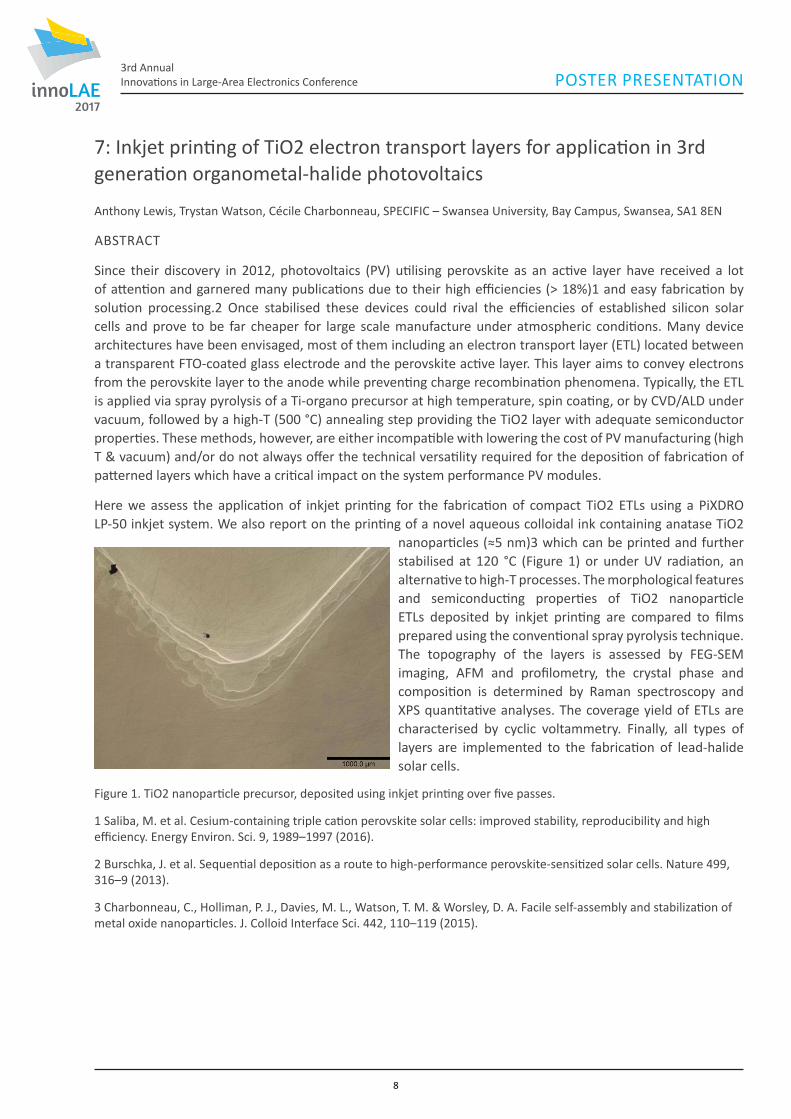
nanoparticles (≈5 nm)3 which can be printed and further stabilised at 120 °C (Figure 1) or under UV radiation, an alternative to high-T processes. The morphological features and semiconducting properties of TiO2 nanoparticle ETLs deposited by inkjet printing are compared to films prepared using the conventional spray pyrolysis technique. The topography of the layers is assessed by FEG-SEM imaging, AFM and profilometry, the crystal phase and composition is determined by Raman spectroscopy and XPS quantitative analyses. The coverage yield of ETLs are characterised by cyclic voltammetry. Finally, all types of layers are implemented to the fabrication of lead-halide solar cells.
Figure 1. TiO2 nanoparticle precursor, deposited using inkjet printing over five passes.
1 Saliba, M. et al. Cesium-containing triple cation perovskite solar cells: improved stability, reproducibility and high efficiency. Energy Environ. Sci. 9, 1989–1997 (2016).
2 Burschka, J. et al. Sequential deposition as a route to high-performance perovskite-sensitized solar cells. Nature 499, 316–9 (2013).
3 Charbonneau, C., Holliman, P. J., Davies, M. L., Watson, T. M. & Worsley, D. A. Facile self-assembly and stabilization of metal oxide nanoparticles. J. Colloid Interface Sci. 442, 110–119 (2015).
8

2017
3rd AnnualInnovations in Large-Area Electronics ConferencePOSTER PRESENTATION
8: Quality-Control of UV Offset Lithographically Printed Electronic-Ink by THz Technology
Yang Zenga, Bob Stevensb, Robert Donnana, Bin Yangc* a School of Electronics and Computer Sciences, Queen Mary University of London, Mile End Road, London E1 4NS, UK; b Nottingham Trent University, Burton Street, Nottingham NG1 4BU, UK; c Department of Electronic and Electrical Engineering, University of Chester, Thornton Science Park, Chester CH2 4NU, UK, [email protected]
ABSTRACT
In this work, we present a novel quality-monitor method of inkjet-printed electronics based on terahertz (THz) sensing. Specifically, two different approaches are proposed, namely THz reflection spectroscopy and THz near-field scanning imaging (NSI). Sintered and un-sintered dielectric patterns printed on different flexible substrates are tested in both systems. THz reflection spectroscopy is firstly used to observe the broadband reflected spectra of the ink. The complex dielectric constants of the ink are quantitatively extracted to reveal ink quality as a whole. THz NSI is then proposed as a more localized and higher resolution investigation method. Intuitive near-field imaging of the ink quality in localized detail is achieved. The results show that THz sensing methods can clearly distinguish sintered and un-sintered printed pat- terns. This work will be of great significant and inspiration for the development of a real-time non-contact quality control system for large area printed electronic-inks.
BIOGRAPHY
Dr. Bin Yang received his MSc and PhD degrees in Electronic Engineering in 2004 and 2008 respectively from Queen Mary University of London (QMUL), UK. After his PhD, Dr Yang remained in the Antenna and Electromagnetics Group of QMUL as a Postdoctoral Researcher. In September 2013, he moved to the University of Bolton as a Lecturer and then joined the University of Chester as a Senior Lecturer in September 2015. His research includes the development of Terahertz (THz) measurement systems and the applications in material, biology and chemistry sciences.
9: Inkjet Flex: Roll to Roll Digital Inkjet Printing of Copper Based Circuits
Steven Bagshaw, CPI
ABSTRACT
The presentation will describe the recently installed capability at CPI, known as Inkjet Flex. Inkjet Flex allows clients to digitally print their own copper based circuit designs onto PET substrates in a roll to roll manner. The technology is ideal for the new product development of antennas, sensors, electrodes, flexible pcbs and many other printed electronics applications. CPI is providing the technology on an initial prototyping basis with a route to upscale to larger production volumes. Using Inkjet Flex the length of design can be printed in km and with a web width of 282.2mm
The talk will provide examples of the scientific challenges CPI faced to get the capability up and running alongside a diverse range of new product examples from academia, SMES and industry who are using the line to develop innovative applications from the UK.
BIOGRAPHY
Steven Bagshaw is responsible for the sales and project management of CPI’s copper inkjet printing capability known as Inkjet Flex. Since the technology was acquired in 2015, Steven has created the online and offline sales channels alongside the implementation of the marketing and sales communication plan. Steven’s expertise lies
9

2017
3rd AnnualInnovations in Large-Area Electronics Conference POSTER PRESENTATION
in the area of printed electronics and its role in the development of the internet of things and industry 4.0.
Previously Steven held marketing positions at CPI, where he was responsible for managing the marketing operations of CPI’s printable electronics division. Steven’s role was to provide an end user focus in the scale up and commercialisation of products and processes related to printable electronics. He has extensive knowledge in emerging technology areas such as intelligent print, printed lighting and enabling technologies such as materials integration and barrier encapsulation.
During his time at CPI Steven has a track record of delivering the successful dissemination of a number projects, including both commercial and collaborative research and development. Steven has also provided strategic marketing direction to a number of start-up companies in the field of printed electronics.
Prior to joining CPI in 2008, Steven graduated from Northumbria University with a Business Studies degree.
10: Controlling and assessing the quality of Aerosol Jet Printed features for large area and flexible electronics
Michael Smith, Yeonsik Choi, Chess Boughey, Sohini Kar-Narayan* Department of Materials Science and Metallurgy, University of Cambridge, UK
ABSTRACT
Additive manufacturing promises to be the future of consumer device production 1,2. Patterning electronic circuits over large areas is of particular interest, especially given the advance of the ‘Internet of Things’ and the forecast of a dramatic increase in the number connected devices. Aerosol Jet Printing (AJP) is a relatively new additive manufacturing technique, capable of printing features down to 10 μm, which offers an alternative to traditional methods in this area such as inkjet printing. However, the relative infancy of the technique, along with the large number of variables, means that the process is not completely understood.
Previous studies have identified how some of the main parameters in AJP affect the morphology of a printed silver line 3. This work investigates some other, more subtle variables that nonetheless have a significant impact on the quality of deposition. An optical method to quantify two of the main aberrations in AJP is also presented and correlated to the deposition parameters and electrical properties of printed silver lines. Using flexible substrates, the bending performance is also assessed.
One of the key observations highlighted is the sensitivity of the process to the ink-substrate combination. As
Controlling and assessing the quality of Aerosol Jet Printed features for large area and flexible electronics
Michael Smith, Yeonsik Choi, Chess Boughey, Sohini Kar-Narayan* Department of Materials Science and Metallurgy, University of Cambridge, UK
Additive manufacturing promises to be the future of consumer device production 1,2. Patterning electronic circuits over large areas is of particular interest, especially given the advance of the ‘Internet of Things’ and the forecast of a dramatic increase in the number connected devices. Aerosol Jet Printing (AJP) is a relatively new additive manufacturing technique, capable of printing features down to 10 μm, which offers an alternative to traditional methods in this area such as inkjet printing. However, the relative infancy of the technique, along with the large number of variables, means that the process is not completely understood.
Previous studies have identified how some of the main parameters in AJP affect the morphology of a printed silver line 3. This work investigates some other, more subtle variables that nonetheless have a significant impact on the quality of deposition. An optical method to quantify two of the main aberrations in AJP is also presented and correlated to the deposition parameters and electrical properties of printed silver lines. Using flexible substrates, the bending performance is also assessed.
One of the key observations highlighted is the sensitivity of the process to the ink-substrate combination. As a result, a framework for arriving at an acceptable set of deposition parameters for any given application is devised by applying the conclusions reached from this work, as well as results determined elsewhere. It is hoped that this will allow more straightforward use of Aerosol Jet Printing to applications within large area and flexible electronics.
References 1. Huang SH, Liu P, Mokasdar A, Hou L. Additive manufacturing and its societal impact: a literature review. Int J Adv
Manuf Technol. 2013;67(5-8):1191-1203. doi:10.1007/s00170-012-4558-5.
2. O’Donnell J, Kim M, Yoon H-S. A Review on Electromechanical Devices Fabricated by Additive Manufacturing. J Manuf Sci Eng. 2016;139(1):10801. doi:10.1115/1.4033758.
3. Mahajan A, Frisbie CD, Francis LF. Optimization of Aerosol Jet Printing for High-Resolution, High-Aspect Ratio Silver Lines. ACS Appl Mater Interfaces. 2013;5(11):4856-4864. doi:10.1021/am400606y.
Figure 1 - The influence of substrate temperature on the morphology of an aerosol jet printed line
Figure 2 – An example of how aerosol jet deposition can be improved using the proposed framework
10

2017
3rd AnnualInnovations in Large-Area Electronics ConferencePOSTER PRESENTATION
a result, a framework for arriving at an acceptable set of deposition parameters for any given application is devised by applying the conclusions reached from this work, as well as results determined elsewhere. It is hoped that this will allow more straightforward use of Aerosol Jet Printing to applications within large area and flexible electronics.
References
1. Huang SH, Liu P, Mokasdar A, Hou L. Additive manufacturing and its societal impact: a literature review. Int J Adv Manuf Technol. 2013;67(5-8):1191-1203. doi:10.1007/s00170-012-4558-5.
2. O’Donnell J, Kim M, Yoon H-S. A Review on Electromechanical Devices Fabricated by Additive Manufacturing. J Manuf Sci Eng. 2016;139(1):10801. doi:10.1115/1.4033758.
3. Mahajan A, Frisbie CD, Francis LF. Optimization of Aerosol Jet Printing for High-Resolution, High-Aspect Ratio Silver Lines. ACS Appl Mater Interfaces. 2013;5(11):4856-4864. doi:10.1021/am400606y.
BIOGRAPHY
I am a second year PhD student in the Department of Materials Science and Metallurgy, University of Cambridge. I studied Natural Sciences for my undergraduate degree, also at Cambridge, with emphasis on the physical sciences and specialising in materials science towards the end of my degree. The principal research focus of my PhD is developing biological sensors using piezoelectric nanomaterials. My interest in large area electronics arises from using an aerosol jet printer to fabricate parts of these sensors, as well as other devices using similar materials.
11: Electrical Metrology for Printed Electronics
Adam Lewis and Martin Wickham *[email protected], National Physical Laboratory, Teddington, UK
ABSTRACT
The printed electronics market doubled from 2014 to 2015 and a similar growth is predicted for 20161. There are numerous applications for printed electronics continually being explored and therefore it is important to have a method to evaluate the quality of the fabricated devices in order to maintain output quality and reduce wastage. Typically printed electronics are fabricated either on a roll-to-roll system or on a flat-bed printer system. The approach in our work is compatible with both of these common production methods. The electrical metrology is based on inductive sensors which is contactless and can be operated at high-speed.
Using inductive sensors, eddy currents are induced perpendicular to the magnetic flux and flow in closed loops. Eddy currents concentrate close to the surface near the excitation coil and the current density decreases exponentially with depth. This is because eddy currents flowing in the sample under test at any depth produce magnetic fields which oppose the primary field and hence reduce the net magnetic flux. The depth at which the eddy current density has decreased by 1/e is referred to as the standard depth of penetration (δ). The effect of frequency (f) on the standard depth of penetration can be approximated by (1), where μ and σ denote the magnetic permeability and electrical conductivity respectively.
The frequency can be modified to vary the penetration depth and consequently the effect of thickness when measuring electrical conductivity. Here, we investigate the performance of the sensors operating at different frequencies. The results identified the optimum frequency of the sensors for the samples under test. The sensors have been demonstrated operating at high speeds, comparable with typical roll-to-roll printed speeds for printed electronics. Additionally we have developed a low-cost circuit to enable measurements at the
Electrical Metrology for Printed Electronics Adam Lewis and Martin Wickham *[email protected], National Physical Laboratory, Teddington, UK
The printed electronics market doubled from 2014 to 2015 and a similar growth is predicted for 20161. There are numerous applications for printed electronics continually being explored and therefore it is important to have a method to evaluate the quality of the fabricated devices in order to maintain output quality and reduce wastage. Typically printed electronics are fabricated either on a roll-to-roll system or on a flat-bed printer system. The approach in our work is compatible with both of these common production methods. The electrical metrology is based on inductive sensors which is contactless and can be operated at high-speed.
Using inductive sensors, eddy currents are induced perpendicular to the magnetic flux and flow in closed loops. Eddy currents concentrate close to the surface near the excitation coil and the current density decreases exponentially with depth. This is because eddy currents flowing in the sample under test at any depth produce magnetic fields which oppose the primary field and hence reduce the net magnetic flux. The depth at which the eddy current density has decreased by 1/e is referred to as the standard depth of penetration (δ). The effect of frequency (f) on the standard depth of penetration can be approximated by (1), where µ and σ denote the magnetic permeability and electrical conductivity respectively.
𝛿𝛿 ≈ 1√𝜋𝜋𝜋𝜋𝜋𝜋𝜋𝜋
(1)
The frequency can be modified to vary the penetration depth and consequently the effect of thickness when measuring electrical conductivity. Here, we investigate the performance of the sensors operating at different frequencies. The results identified the optimum frequency of the sensors for the samples under test. The sensors have been demonstrated operating at high speeds, comparable with typical roll-to-roll printed speeds for printed electronics. Additionally we have developed a low-cost circuit to enable measurements at the optimised frequency. Contactless inductive sensing using eddy currents can provide information on changes in the electrical properties of samples. This makes it feasible to measure the electrical properties which at present are not monitored in roll-to-roll printed electronics manufacture.
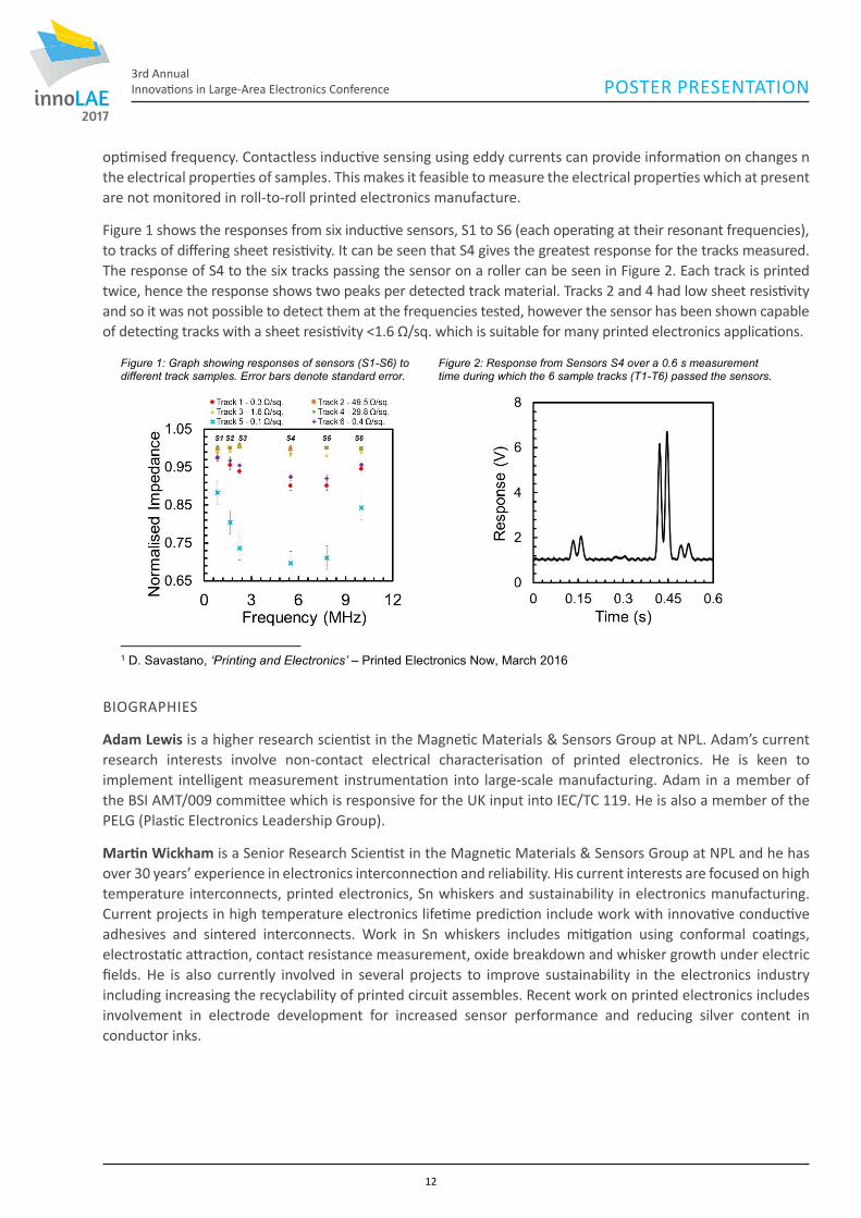
Figure 1 shows the responses from six inductive sensors, S1 to S6 (each operating at their resonant frequencies), to tracks of differing sheet resistivity. It can be seen that S4 gives the greatest response for the tracks measured. The response of S4 to the six tracks passing the sensor on a roller can be seen in Figure 2. Each track is printed twice, hence the response shows two peaks per detected track material. Tracks 2 and 4 had low sheet resistivity and so it was not possible to detect them at the frequencies tested, however the sensor has been shown capable of detecting tracks with a sheet resistivity <1.6 Ω/sq. which is suitable for many printed electronics applications.
1 D. Savastano, ‘Printing and Electronics’ – Printed Electronics Now, March 2016
Figure 1: Graph showing responses of sensors (S1-S6) to different track samples. Error bars denote standard error.
Figure 2: Response from Sensors S4 over a 0.6 s measurement time during which the 6 sample tracks (T1-T6) passed the sensors.
11
2017
3rd AnnualInnovations in Large-Area Electronics Conference POSTER PRESENTATION
optimised frequency. Contactless inductive sensing using eddy currents can provide information on changes n the electrical properties of samples. This makes it feasible to measure the electrical properties which at present are not monitored in roll-to-roll printed electronics manufacture.
Figure 1 shows the responses from six inductive sensors, S1 to S6 (each operating at their resonant frequencies), to tracks of differing sheet resistivity. It can be seen that S4 gives the greatest response for the tracks measured. The response of S4 to the six tracks passing the sensor on a roller can be seen in Figure 2. Each track is printed twice, hence the response shows two peaks per detected track material. Tracks 2 and 4 had low sheet resistivity and so it was not possible to detect them at the frequencies tested, however the sensor has been shown capable of detecting tracks with a sheet resistivity <1.6 Ω/sq. which is suitable for many printed electronics applications.
Electrical Metrology for Printed Electronics Adam Lewis and Martin Wickham *[email protected], National Physical Laboratory, Teddington, UK
The printed electronics market doubled from 2014 to 2015 and a similar growth is predicted for 20161. There are numerous applications for printed electronics continually being explored and therefore it is important to have a method to evaluate the quality of the fabricated devices in order to maintain output quality and reduce wastage. Typically printed electronics are fabricated either on a roll-to-roll system or on a flat-bed printer system. The approach in our work is compatible with both of these common production methods. The electrical metrology is based on inductive sensors which is contactless and can be operated at high-speed.
Using inductive sensors, eddy currents are induced perpendicular to the magnetic flux and flow in closed loops. Eddy currents concentrate close to the surface near the excitation coil and the current density decreases exponentially with depth. This is because eddy currents flowing in the sample under test at any depth produce magnetic fields which oppose the primary field and hence reduce the net magnetic flux. The depth at which the eddy current density has decreased by 1/e is referred to as the standard depth of penetration (δ). The effect of frequency (f) on the standard depth of penetration can be approximated by (1), where µ and σ denote the magnetic permeability and electrical conductivity respectively.
𝛿𝛿 ≈ 1√𝜋𝜋𝜋𝜋𝜋𝜋𝜋𝜋
(1)
The frequency can be modified to vary the penetration depth and consequently the effect of thickness when measuring electrical conductivity. Here, we investigate the performance of the sensors operating at different frequencies. The results identified the optimum frequency of the sensors for the samples under test. The sensors have been demonstrated operating at high speeds, comparable with typical roll-to-roll printed speeds for printed electronics. Additionally we have developed a low-cost circuit to enable measurements at the optimised frequency. Contactless inductive sensing using eddy currents can provide information on changes in the electrical properties of samples. This makes it feasible to measure the electrical properties which at present are not monitored in roll-to-roll printed electronics manufacture.
Figure 1 shows the responses from six inductive sensors, S1 to S6 (each operating at their resonant frequencies), to tracks of differing sheet resistivity. It can be seen that S4 gives the greatest response for the tracks measured. The response of S4 to the six tracks passing the sensor on a roller can be seen in Figure 2. Each track is printed twice, hence the response shows two peaks per detected track material. Tracks 2 and 4 had low sheet resistivity and so it was not possible to detect them at the frequencies tested, however the sensor has been shown capable of detecting tracks with a sheet resistivity <1.6 Ω/sq. which is suitable for many printed electronics applications.
1 D. Savastano, ‘Printing and Electronics’ – Printed Electronics Now, March 2016
Figure 1: Graph showing responses of sensors (S1-S6) to different track samples. Error bars denote standard error.
Figure 2: Response from Sensors S4 over a 0.6 s measurement time during which the 6 sample tracks (T1-T6) passed the sensors.
BIOGRAPHIES
Adam Lewis is a higher research scientist in the Magnetic Materials & Sensors Group at NPL. Adam’s current research interests involve non-contact electrical characterisation of printed electronics. He is keen to implement intelligent measurement instrumentation into large-scale manufacturing. Adam in a member of the BSI AMT/009 committee which is responsive for the UK input into IEC/TC 119. He is also a member of the PELG (Plastic Electronics Leadership Group).
Martin Wickham is a Senior Research Scientist in the Magnetic Materials & Sensors Group at NPL and he has over 30 years’ experience in electronics interconnection and reliability. His current interests are focused on high temperature interconnects, printed electronics, Sn whiskers and sustainability in electronics manufacturing. Current projects in high temperature electronics lifetime prediction include work with innovative conductive adhesives and sintered interconnects. Work in Sn whiskers includes mitigation using conformal coatings, electrostatic attraction, contact resistance measurement, oxide breakdown and whisker growth under electric fields. He is also currently involved in several projects to improve sustainability in the electronics industry including increasing the recyclability of printed circuit assembles. Recent work on printed electronics includes involvement in electrode development for increased sensor performance and reducing silver content in conductor inks.
12

2017
3rd AnnualInnovations in Large-Area Electronics ConferencePOSTER PRESENTATION
12: Solution-Processed Co-planar Nano-Scale Photodetectors by Adhesion Lithography
Gwenhivir Wyatt-Moon, Dimitra G. Georgiadou, James Semple and Thomas D. Anthopoulos
ABSTRACT
As the resolution of devices in the electronics industry has hit the nanoscale, device fabrication costs have rapidly increased. Whilst commercial technologies such as photolithography are able to produce nanoscale feature size, they are costly and unsuitable for large area printable electronics. Research is now focusing on fabrication techniques that can reproduce this small size on flexible substrates without incurring such high costs, such as adhesion lithography (a-Lith). A-Lith is a novel, large scale fabrication technique for producing planar asymmetric nanogap electrodes. Devices have be created with aspect ratios >100000. The technique can be carried out in air and at low temperature making it ideal for the field of plastic electronics.
Here we show a-Lith used together with light sensitive, solution processable semiconductors to create photodetectors with large on/off ratios. This includes the use of Copper Thiocyanate (CuSCN), a visible-blind material, to create highly sensitive Schottky UV photodetectors, for use in different sensor applications including biological and environmental monitoring and analysis.
BIOGRAPHY
Gwen is a PhD Student within the Experimental Solid State Physics group at Imperial College London, under the supervision of Professor Thomas Anthopoulos. She is currently working on optimising the novel fabrication technique adhesion lithography (a-Lith), with particular focus on applications for optoelectronic devices such as organic light emitting diodes and photodetectors. Gwen gained her MRes in plastic electronics from Imperial College London and has previously worked for a medical devices company focusing on novel gas sensors and flow rheometry systems. Prior to this she gained her BEng in electrical engineering at Swansea University. Her current research interests include innovative fabrication techniques, materials, and devices for the plastic electronics field.
13: Market opportunities for Large Area Electronics
Guillaume Chansin, IDTechEx Research
ABSTRACT
This presentation will give an overview of the latest analysis from IDTechEx. In particular, it will cover the following aspects of large area electronics:• The commercialization of organic electronics beyond OLED• Status of flexible hybrid electronics• How printed sensors can compete• Technology trends in display industry• Emerging applications in Wearables, Healthcare, and IoT
13

2017
3rd AnnualInnovations in Large-Area Electronics Conference POSTER PRESENTATION
Global wearable technology forecast
BIOGRAPHY
Dr Guillaume Chansin is a Senior Technology Analyst at IDTechEx Research. Based in Cambridge (UK), he interprets the latest trends and market data in several industries, such as printed electronics, sensors, flexible displays and wearable electronics. His previous academic research includes three-dimensional fabrication with nanoimprint lithography and synthetic nanopore devices. Guillaume published several research papers in leading nanotechnology journals and received his PhD from Imperial College London. Before joining IDTechEx, he worked on the development of flexible e-paper displays at Plastic Logic. He is fluent in French and English and gives presentations in both languages. www.IDTechEx.com
14: Metal hexagonal grids and transparent conductors for OLEDs anode
Salvatore Aprano,1 Luca Iannuzzi,2 Ludovico Migliaccio,3,4 Claudia Diletto,4 Maria Grazia Maglione,4 Paolo Tassini,4 Carla Minarini,4 Paola Manini,3 Alessandro Pezzella,3 Alfredo Rubino.1 1Università degli Studi di Salerno – Department of Industrial Engineering, Via Giovanni Paolo II n.132, Fisciano, SA, Italy 2INSTM – Consorzio Interuniversitario Nazionale per la Scienza e Tecnologia dei Materiali, Via Giusti n.9, Firenze, Italy 3 Università degli Studi di Napoli Federico II - Department of Chemical Sciences, Via Cintia n.4, Napoli, Italy 4 ENEA - Agenzia Nazionale per le Nuove Tecnologie, l’Energia e lo Sviluppo Economico Sostenibile, SSPT-PROMAS-NANO, C. R. Portici, P.le E. Fermi n.1, Portici, NA, Italy
ABSTRACT
Large area organic light emitting diodes (OLEDs) are becoming very attractive devices for next generation of lighting applications. Anyway, the limited conductivity of the transparent anodic material (mostly ITO, indium tin oxide) leads to a lateral voltage drop along this contact, which reduces the current flow in this type of devices [1] so decreasing their performances. A simple way to overcome the low conductivity of the ITO, without
14
2017
3rd AnnualInnovations in Large-Area Electronics ConferencePOSTER PRESENTATION
replacing it, and keep a good transparency of the anode, is to fabricate a metal grid on the ITO surface. In the literature, a hexagonal shape of the anodic metal grid is reported to have the lowest voltage loss [2] and the most established approaches to characterize it take into account the conductivity of the metal only [3]. In this work, various types of hexagonal metal grids have been prepared, using the lift-off method to define the metal lines, and coupled with ITO or PEDOT:PSS as the anodic material, measuring the resulting sheet resistance and optical transmittance. It has been observed that conductivity of the transparent conductor plays a key role in the behavior of these structures, and therefore the layout of the metal grids has to be tailored to obtain a good trade-off between electrical and optical properties and eventually use them in OLEDs.
1. Neyts K., Marescaux M., Nieto A. U., Elschner A., Lövenich W., Fehse K., Huang Q., Walzer K., and Leo K.; 2006 J. Appl. Phys. 100 114513. 2. Neyts K., Real A., Marescaux M., Mladenovski S., and Beeckman J.; 2008 J. Appl. Phys. 103 093113. 3. Ghosh D. S., Chen T. L., and Pruneri V.; 2009 Appl. Phys. Lett. 96, 041109.
BIOGRAPHY
Laurea degree in Electronic Engineering (5 years course) at Università di Roma “Tor Vergata”. In ENEA from 2000, with Laboratory of Nanomaterials and Devices (NANO). His interests have spanned from amorphous and polycrystalline silicon TFTs to organic devices, OLEDs, OTFTs, sensors, RFID, focusing on design, processing and characterization of materials, devices and circuits. He coordinated the ENEA scientific activities in Italian and European projects and has been responsible for the specifications and the purchase of complex and high value instrumentations and process systems. He is co-author of over 60 publications and communications to conferences and two patents. He is member of Organic and Printed Electronics Association (OEA), Photonics21 and Italian Association of Engineers.
15: Environmental Stability of the Density of States in Evaporated DNTT Films
Nor K Za’aba and D Martin Taylor School of Electronic Engineering, Bangor University, Dean Street, Bangor, Gwynedd LL57 1UT, UK
ABSTRACT
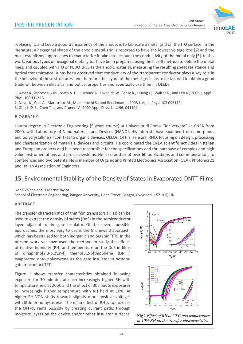
The transfer characteristics of thin film transistors (TFTs) can be used to extract the density of states (DoS) in the semiconductor layer adjacent to the gate insulator. Of the several possible approaches, the most easy to use is the Grünewald approach, which has been used for both inorganic and organic TFTs. In the present work we have used the method to study the effects of relative humidity (RH) and temperature on the DoS in films of dinaphtho[2,3-b:2’,3’-f] thieno[3,2-b]thiophene (DNTT) evaporated onto polystyrene as the gate insulator in bottom-gate topcontact TFTs.
Figure 1 shows transfer characteristics obtained following exposure for 30 minutes at each increasingly higher RH with temperature held at 20oC and the effect of 30 minute exposures to increasingly higher temperature with RH held at 10%. At higher RH VON shifts towards slightly more positive voltages with little or no hysteresis. The main effect of RH is to increase the OFF-currents possibly by creating current paths through moisture layers on the device and/or other insulator surfaces.
Environmental Stability of the Density of States in Evaporated DNTT Films Nor K Za’aba and D Martin Taylor
School of Electronic Engineering, Bangor University, Dean Street, Bangor,
Gwynedd LL57 1UT, UK.
Abstract The transfer characteristics of thin film transistors (TFTs) can be used to extract the density of states (DoS) in the semiconductor layer adjacent to the gate insulator. Of the several possible approaches, the most easy to use is the Grünewald approach, which has been used for both inorganic and organic TFTs.
In the present work we have used the method to study the effects of relative humidity (RH) and temperature on the DoS in films of dinaphtho[2,3-b:2',3'-f] thieno[3,2-b]thiophene (DNTT) evaporated onto polystyrene as the gate insulator in bottom-gate top-contact TFTs. Figure 1 shows transfer characteristics obtained following exposure for 30 minutes at each increasingly higher RH with temperature held at 20oC and the effect of 30 minute exposures to increasingly higher temperature with RH held at 10%. At higher RH VON shifts towards slightly more positive voltages with little or no hysteresis. The main effect of RH is to increase the OFF-currents possibly by creating current
paths through moisture layers on the device and/or other insulator surfaces. Only minimal recovery was observed on reducing RH. On the otherhand, increasing temperature resulted in significant positive shifts in VON accompanied by increasing hysteresis and but with overnight recovery at lower temperature. Figure 2 shows the density of states extracted from the transfer characteristics and plotted relative to the mobility edge, which we associated with the start of extended states at EV. The plots suggest that the main effect of RH and temperature is on the gate insulator. DNTT appears resilient to such changes and important feature in device applications. Acknowledgement The authors are grateful to Dr J J Morrison, Manchester University for samples of DNTT. NKZ is grateful to MARA for the award of a PhD studentship.
20 10 0 -10 -20 -30 -40 -50 -60 -70-13
-12
-11
-10
-9
-8
-7
-6
-5
0 -20 -40 -600.0
0.2
0.4
0.6
0.8
1.0
80% RH
I D (
A)
VG (V)
20% RH
80% RH
log 1
0 (I D
/A)
VG (V)
VD=-1V
20% RH
20 10 0 -10 -20 -30 -40 -50 -60 -70-12
-11
-10
-9
-8
-7
-6
0 -20 -40 -600.0
0.2
0.4
0.6
0.8 20 C 30 C 40 C 50 C 60 C 70 C 80 C 90 C recovery
I D (A
)
VG (V)
20 C 30 C 40 C 50 C 60 C 70 C 80 C 90 C recovery
log
(I D/A)
VG (V)
Fig 1 Effect of RH at 20oC and temperature at 10% RH on the transfer characteristics
0.0 0.1 0.2 0.3 0.41016
1017
1018
1019
1020
1021
1022
20% RH 30% RH 40% RH 50% RH 60% RH 70% RH 80% RH
DoS
(cm
-3eV
-1)
E-EV (eV)
0.0 0.1 0.2 0.3 0.41016
1017
1018
1019
1020
1021
20 C 30 C 40 C 50 C 60 C 70 C 80 C 90 C recovery
DoS
(cm
-3eV
-1)
E-EV (eV)
Fig 2 Density of States in DNTT plotted relative to the mobility edge at EV
15

2017
3rd AnnualInnovations in Large-Area Electronics Conference POSTER PRESENTATION
Only minimal recovery was observed on reducing RH. On the otherhand, increasing temperature resulted in significant positive shifts in VON accompanied by increasing hysteresis and but with overnight recovery at lower temperature.
Figure 2 shows the density of states extracted from the transfer characteristics and plotted relative to the mobility edge, which we associated with the start of extended states at EV. The plots suggest that the main effect of RH and temperature is on the gate insulator. DNTT appears resilient to such changes and important feature in device applications.
Acknowledgement
The authors are grateful to Dr J J Morrison, Manchester University for samples of DNTT. NKZ is grateful to MARA for the award of a PhD studentship.
BIOGRAPHIES
Nor Za’aba is currently in the third year of her PhD studies having obtained her first degree in Computational and Electronic Physics from University of Malaya. Some of the results from her PhD studies were reported in an oral presentation at the International Conference on Electronic Materials held in Singapore in July 2016
Martin Taylor is an Emeritus Professor at Bangor University. He has undertaken research into organic electronic devices for many years and has published papers on organic Schottky diodes, MIS capacitors, transistors and circuits. In his most recent paper with co-authors from SmartKem Ltd, he reported the shortest stage-delay time for a ring oscillator based on a solution-processed p-type semiconductor.
Environmental Stability of the Density of States in Evaporated DNTT Films Nor K Za’aba and D Martin Taylor
School of Electronic Engineering, Bangor University, Dean Street, Bangor,
Gwynedd LL57 1UT, UK.
Abstract The transfer characteristics of thin film transistors (TFTs) can be used to extract the density of states (DoS) in the semiconductor layer adjacent to the gate insulator. Of the several possible approaches, the most easy to use is the Grünewald approach, which has been used for both inorganic and organic TFTs.
In the present work we have used the method to study the effects of relative humidity (RH) and temperature on the DoS in films of dinaphtho[2,3-b:2',3'-f] thieno[3,2-b]thiophene (DNTT) evaporated onto polystyrene as the gate insulator in bottom-gate top-contact TFTs. Figure 1 shows transfer characteristics obtained following exposure for 30 minutes at each increasingly higher RH with temperature held at 20oC and the effect of 30 minute exposures to increasingly higher temperature with RH held at 10%. At higher RH VON shifts towards slightly more positive voltages with little or no hysteresis. The main effect of RH is to increase the OFF-currents possibly by creating current
paths through moisture layers on the device and/or other insulator surfaces. Only minimal recovery was observed on reducing RH. On the otherhand, increasing temperature resulted in significant positive shifts in VON accompanied by increasing hysteresis and but with overnight recovery at lower temperature. Figure 2 shows the density of states extracted from the transfer characteristics and plotted relative to the mobility edge, which we associated with the start of extended states at EV. The plots suggest that the main effect of RH and temperature is on the gate insulator. DNTT appears resilient to such changes and important feature in device applications. Acknowledgement The authors are grateful to Dr J J Morrison, Manchester University for samples of DNTT. NKZ is grateful to MARA for the award of a PhD studentship.
20 10 0 -10 -20 -30 -40 -50 -60 -70-13
-12
-11
-10
-9
-8
-7
-6
-5
0 -20 -40 -600.0
0.2
0.4
0.6
0.8
1.0
80% RH
I D (
A)
VG (V)
20% RH
80% RH
log 1
0 (I D
/A)
VG (V)
VD=-1V
20% RH
20 10 0 -10 -20 -30 -40 -50 -60 -70-12
-11
-10
-9
-8
-7
-6
0 -20 -40 -600.0
0.2
0.4
0.6
0.8 20 C 30 C 40 C 50 C 60 C 70 C 80 C 90 C recovery
I D (A
)
VG (V)
20 C 30 C 40 C 50 C 60 C 70 C 80 C 90 C recovery
log
(I D/A)
VG (V)
Fig 1 Effect of RH at 20oC and temperature at 10% RH on the transfer characteristics
0.0 0.1 0.2 0.3 0.41016
1017
1018
1019
1020
1021
1022
20% RH 30% RH 40% RH 50% RH 60% RH 70% RH 80% RH
DoS
(cm
-3eV
-1)
E-EV (eV)
0.0 0.1 0.2 0.3 0.41016
1017
1018
1019
1020
1021
20 C 30 C 40 C 50 C 60 C 70 C 80 C 90 C recovery
DoS
(cm
-3eV
-1)
E-EV (eV)
Fig 2 Density of States in DNTT plotted relative to the mobility edge at EV
16: Refractive index patterning of molecular hybrid for photonics
Stefan Bachevillier1, Natalie Stingelin1,2, Paul Stavrinou1,3, Andreas Hafner4 [1] Centre for Plastic Electronics & Department of Materials, Imperial College London, SW7 2AZ, UK; [2] School of Materials Science and Engineering, Georgia Tech, GA 30332-0245, USA; [3] Department of Engineering Science, University of Oxford, OX1 3PJ, UK; [4] BASF AG, Basel BS, 4057, Switzerland
ABSTRACT
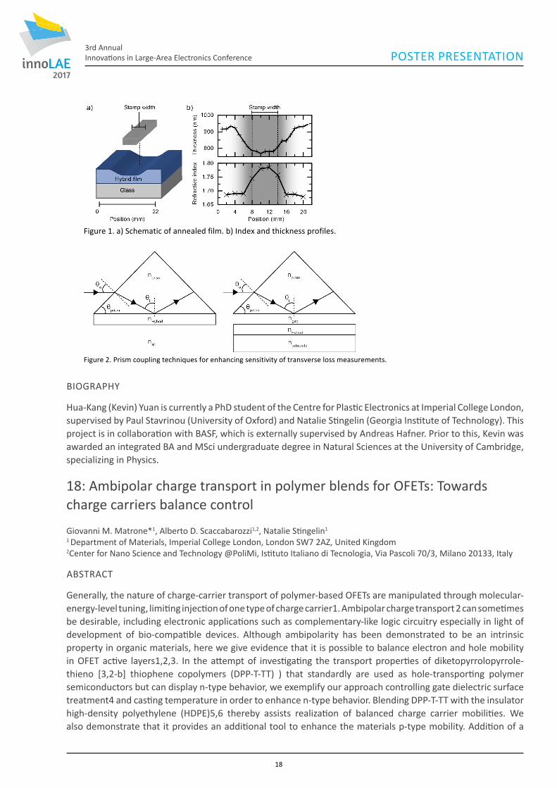
After the use of highly efficient but expensive inorganic optical materials, solutionprocessable polymers and hybrids have drawn more and more interest. Our group have recently developed a novel polymer-based hybrid optical material exhibiting an outstanding set of optical and material properties (Figure 1).
Even more remarkably, the refractive index can be tuned by either changing the inorganic content or locally via scalable patterning techniques. In this work, distinct methods will be presented. One of them, called hot-stamping can be used to fabricate waveguides (high refractive index core surrounded by lower index regions) as shown in Figure 2. These promising results open the way to solution-processed, high through- put and low-cost photonic structures.
Another part of this project is focused on reliable optical characterisation of these properties using a specific spectrometry method. This technique can be applied to non-destructive mapping of optical thin film properties but also to in situ annealing.
16

2017
3rd AnnualInnovations in Large-Area Electronics ConferencePOSTER PRESENTATION
BIOGRAPHY
Stefan Bachevillier is currently a PhD student at the department of Materials, Imperial College London within the Centre for Plastic Electronics and with Professors Natalie Stingelin and Paul Stavrinou as supervisors. Prior to this, he obtained a Master of Research at University of Bordeaux (IMS laboratory) and the degree of Engineer in Materials Science at ENSCBP of Bordeaux. During his Master’s degree, he had the opportunity to conduct research at several research companies such as Nikon and Essilor International Joint Research Center (Tokyo, Japan), Cambridge Display Technology Ltd. and Plastic Logic Ltd.
Refractive index patterning of molecular hybrid for photonics
Stefan Bachevillier1, Natalie Stingelin1,2, Paul Stavrinou1,3, Andreas Hafner4
[1] Centre for Plastic Electronics & Department of Materials, Imperial College London, SW7 2AZ, UK;[2] School of Materials Science and Engineering, Georgia Tech, GA 30332-0245, USA; [3] Department of Engineering Science, University of Oxford, OX1 3PJ, UK; [4] BASF AG, Basel BS, 4057, Switzerland After the use of highly efficient but expensive inorganic optical materials, solution-processable polymers and hybrids have drawn more and more interest. Our group have recently developed a novel polymer-based hybrid optical material exhibiting an outstanding set of optical and material properties (Figure 1). Even more remarkably, the refractive index can be tuned by either changing the inorganic content or locally via scalable patterning techniques. In this work, distinct methods will be presented. One of them, called hot-stamping can be used to fabricate waveguides (high refractive index core surrounded by lower index regions) as shown in Figure 2. These promising results open the way to solution-processed, high through- put and low-cost photonic structures. Another part of this project is focused on reliable optical characterisation of these properties using a specific spectrometry method. This technique can be applied to non-destructive mapping of optical thin film properties but also to in situ annealing.
Figure1.Refractiveindexrangesofdifferentmaterialcategoriesincomparisonwithourtunablerefractiveindexhybridmaterial.
Figure2.Refractiveindexmappingofhybridthinfilmafterhotstampingpatterning.
Key words: Photonics - Functional inorganic/organic hybrids - Solution processable - Refractive index - Patterning
Biography: Stefan Bachevillier is currently a PhD student at the department of Materials, Imperial College London within the Centre for Plastic Electronics and with Professors Natalie Stingelin and Paul Stavrinou as supervisors. Prior to this, he obtained a Master of Research at University of Bordeaux (IMS laboratory) and the degree of Engineer in Materials Science at ENSCBP of Bordeaux. During his Master’s degree, he had the opportunity to conduct research at several research companies such as Nikon and Essilor International Joint Research Center (Tokyo, Japan), Cambridge Display Technology Ltd. and Plastic Logic Ltd. (Cambridge, UK).
0 5 10 150
5
10
15
y(m
m)
x (mm)
1.76
1.80
1.84
1.88
1.92
Refractive index(550nm)
17: Enhanced sensitivity for optical loss measurement in planar thin-films for light management
Hua-Kang Yuan, Imperial College London
ABSTRACT
Light management is to control the behaviour of light, often within or at the interface of optoelectronic devices. An organic-inorganic hybrid material benefits from processing advantages of organics and high refractive indices of inorganics. We focus on a titanium oxide hydrate system combined with common bulk polymers. In particular, we target thin-film structures of a few microns in thickness. A simple method of inplane patterning refractive index is a step towards waveguiding which would allow for a cut-back method approach (figure 1). Traditional Beer-Lambert approaches for measuring optical losses can only provide an upper limit estimate. This sensitivity is highly limited when considering the low-losses required for mid-range optical applications, on the order of 0.1 cm-1. For intensity based measurements, improving the sensitivity requires an increase in the optical path length. Instead, a sensitive technique suitable for simple planar thin films is required. A number of systems were modelled to measure optical losses in films of 1 micron thick in the visible region. The presented techniques utilise evanescent waves and total internal reflection to increase optical path length through the material. It was found that a new way of using prism coupling figure 2) provides the greatest improvement in sensitivity. In keeping the requirements on the material simple, this method for measuring loss is well suited to any future developments of new materials in thinfilm structures.
17
2017
3rd AnnualInnovations in Large-Area Electronics Conference POSTER PRESENTATION
Postersubmission:Hua-KangYuan
Abstract(forposterpresentation)
Title:Enhancedsensitivityforopticallossmeasurementinplanarthin-filmsforlightmanagement Keywords:opticallosses,thin-films,polymer,waveguiding,modellingLightmanagementistocontrolthebehaviouroflight,oftenwithinorattheinterfaceofoptoelectronicdevices.Anorganic-inorganichybridmaterialbenefitsfromprocessingadvantagesoforganicsandhighrefractiveindicesofinorganics.Wefocusonatitaniumoxidehydratesystemcombinedwithcommonbulkpolymers.Inparticular,wetargetthin-filmstructuresofafewmicronsinthickness.Asimplemethodofin-planepatterningrefractiveindexisasteptowardswaveguidingwhichwouldallowforacut-backmethodapproach(figure1).TraditionalBeer-Lambertapproachesformeasuringopticallossescanonlyprovideanupperlimitestimate.Thissensitivityishighlylimitedwhenconsideringthelow-lossesrequiredformid-rangeopticalapplications,ontheorderof0.1cm-1.Forintensitybasedmeasurements,improvingthesensitivityrequiresanincreaseintheopticalpathlength.Instead,asensitivetechniquesuitableforsimpleplanarthinfilmsisrequired.Anumberofsystemsweremodelledtomeasureopticallossesinfilmsof1micronthickinthevisibleregion.Thepresentedtechniquesutiliseevanescentwavesandtotalinternalreflectiontoincreaseopticalpathlengththroughthematerial.Itwasfoundthatanewwayofusingprismcoupling(figure2)providesthegreatestimprovementinsensitivity.Inkeepingtherequirementsonthematerialsimple,thismethodformeasuringlossiswellsuitedtoanyfuturedevelopmentsofnewmaterialsinthin-filmstructures.
Figure1.a)Schematicofannealedfilm.b)Indexandthicknessprofiles.
Figure2.Prismcouplingtechniquesforenhancingsensitivityoftransverselossmeasurements.
Biography
Hua-Kang(Kevin)YuaniscurrentlyaPhDstudentoftheCentreforPlasticElectronicsatImperialCollegeLondon,supervisedbyPaulStavrinou(UniversityofOxford)andNatalieStingelin(GeorgiaInstituteofTechnology).ThisprojectisincollaborationwithBASF,whichisexternallysupervisedbyAndreasHafner.Priortothis,KevinwasawardedanintegratedBAandMSciundergraduatedegreeinNaturalSciencesattheUniversityofCambridge,specializinginPhysics.
BIOGRAPHY
Hua-Kang (Kevin) Yuan is currently a PhD student of the Centre for Plastic Electronics at Imperial College London, supervised by Paul Stavrinou (University of Oxford) and Natalie Stingelin (Georgia Institute of Technology). This project is in collaboration with BASF, which is externally supervised by Andreas Hafner. Prior to this, Kevin was awarded an integrated BA and MSci undergraduate degree in Natural Sciences at the University of Cambridge, specializing in Physics.
18: Ambipolar charge transport in polymer blends for OFETs: Towards charge carriers balance control
Giovanni M. Matrone*1, Alberto D. Scaccabarozzi1,2, Natalie Stingelin1 1 Department of Materials, Imperial College London, London SW7 2AZ, United Kingdom 2Center for Nano Science and Technology @PoliMi, Istituto Italiano di Tecnologia, Via Pascoli 70/3, Milano 20133, Italy
ABSTRACT
Generally, the nature of charge-carrier transport of polymer-based OFETs are manipulated through molecular-energy-level tuning, limiting injection of one type of charge carrier1. Ambipolar charge transport 2 can sometimes be desirable, including electronic applications such as complementary-like logic circuitry especially in light of development of bio-compatible devices. Although ambipolarity has been demonstrated to be an intrinsic property in organic materials, here we give evidence that it is possible to balance electron and hole mobility in OFET active layers1,2,3. In the attempt of investigating the transport properties of diketopyrrolopyrrole-thieno [3,2-b] thiophene copolymers (DPP-T-TT) ) that standardly are used as hole-transporting polymer semiconductors but can display n-type behavior, we exemplify our approach controlling gate dielectric surface treatment4 and casting temperature in order to enhance n-type behavior. Blending DPP-T-TT with the insulator high-density polyethylene (HDPE)5,6 thereby assists realization of balanced charge carrier mobilities. We also demonstrate that it provides an additional tool to enhance the materials p-type mobility. Addition of a
18

2017
3rd AnnualInnovations in Large-Area Electronics ConferencePOSTER PRESENTATION
commodity polymer will moreover allow fine-tuning of the mechanical properties, a feature that can be of great importance in the printing electronic area, assisting the deposition of more stable active layers.
[1] Y. Li, S. P. Singh, P. Sonar, Adv. Mater. 2010, 43, 4862. [2] L. L. Chua, J. Zaumseil, Nature 2005, 434, 194. [3] R.S. Ashraf, Z. Chen, Chem. Mater. 2011, 23, 768. [4] Scaccabarozzi, A. D.; Stingelin, N.,Advances. J. Mater. Chem. A 2014, 2 (28), 10818−10824. [5] Hellmann, C.; Treat, N. D., J. Polym. Sci., Part B: Polym. Phys. 2015, 53, 304− 310.
BIOGRAPHY
2013 - Bachelor in Science and Materials Engineering ( University Federico II Naples ITA)
2015 – Master degree in Materials Engineering and Nanotechnology ( Politecnico di Milano ITA)
2016 on – PhD student in Natalie Stingelin’s group (Imperial College London) as an Early Stage Researcher in INFORM - Marie Sklodowska-Curie Innovative Training Network
Ambipolar charge transport in polymer blends for OFETs: Towards charge carriers
balance control
Giovanni M. Matrone*1, Alberto D. Scaccabarozzi1,2, Natalie Stingelin1
1 Department of Materials, Imperial College London, London SW7 2AZ, United Kingdom 2Center for Nano Science and Technology @PoliMi, Istituto Italiano di Tecnologia, Via Pascoli 70/3,
Milano 20133, Italy * [email protected] Generally, the nature of charge-carrier transport of polymer-based OFETs are manipulated through molecular-energy-level tuning, limiting injection of one type of charge carrier1. Ambipolar charge transport 2 can sometimes be desirable, including electronic applications such as complementary-like logic circuitry especially in light of development of bio-compatible devices. Although ambipolarity has been demonstrated to be an intrinsic property in organic materials, here we give evidence that it is possible to balance electron and hole mobility in OFET active layers1,2,3. In the attempt of investigating the transport properties of diketopyrrolopyrrole-thieno [3,2-b] thiophene copolymers (DPP-T-TT) ) that standardly are used as hole-transporting polymer semiconductors but can display n-type behavior, we exemplify our approach controlling gate dielectric surface treatment4 and casting temperature in order to enhance n-type behavior. Blending DPP-T-TT with the insulator high-density polyethylene (HDPE)5,6 thereby assists realization of balanced charge carrier mobilities. We also demonstrate that it provides an additional tool to enhance the materials p-type mobility. Addition of a commodity polymer will moreover allow fine-tuning of the mechanical properties, a feature that can be of great importance in the printing electronic area, assisting the deposition of more stable active layers.
[1] Y. Li, S. P. Singh, P. Sonar, Adv. Mater. 2010, 43, 4862. [2] L. L. Chua, J. Zaumseil, Nature 2005, 434, 194. [3] R.S. Ashraf, Z. Chen, Chem. Mater. 2011, 23, 768. [4] Scaccabarozzi, A. D.; Stingelin, N.,Advances. J. Mater. Chem. A 2014, 2 (28), 10818−10824. [5] Hellmann, C.; Treat, N. D., J. Polym. Sci., Part B: Polym. Phys. 2015, 53, 304− 310.
-1.4x10⁻³
-1.2
-1.0
-0.8
-0.6
-0.4
-0.2
0.0
I d (A
)
-60 -50 -40 -30 -20 -10 0Vd (V)
10-11
10-10
10-9
10-8
10-7
10-6
10-5
10-4
I d (A
)
-40 -30 -20 -10 0Vg (V)
10-8
10-7
10-6
10-5
10-4
Id (A
)
-30 -20 -10 0 10 20 30
Vg (V)
-1.4x10⁻³
-1.2
-1.0
-0.8
-0.6
-0.4
-0.2
0.0
I d (A
)
-60 -50 -40 -30 -20 -10 0Vd (V)
Vd = -20
Representative transfer (a) and output (b) characteristics of DPP-T-TT:HDPE 60:40 bottom-gate bottom-contact field-effect transistors. Source-drain voltages are -1V and -40V. Source-gate voltages in the outputs ranges from 0 V to -40 V with -10 V step. Ambipolar transfer characteristics (c), source-drain voltage is -20V.
(b) (a
) (c)
19: Interconnection Technologies for Integration of Active Devices with Printed Plastic Electronics
Guangbin Dou and Andrew S. Holmes Department of Electrical and Electronic Engineering, Imperial College London, London SW7 2AZ, United Kingdom
ABSTRACT
Printed electronic circuits on low-temperature plastic substrates have enormous potential across a range of consumer markets including automotive windows, wearable devices, healthcare devices and smart labels. Many of these applications require a combination of both printed electronics, which offers large area and flexibility at low cost, and conventional silicon electronics which allows much greater functionality. Currently the main technique used for integrating silicon devices with plastic electronics is Isotropic Conductive Adhesive (ICA) packaging. With this approach, a conductive adhesive (typically a silver-loaded paste) is printed onto the substrate at sites where electrical connection is required. The silicon device is then placed in position, and the adhesive is cured. The same approach is also being used to mount flexible plastic electronic chips on plastic substrates. In this project we will investigate the use of Non Conductive Adhesive (NCA) packaging as an alternative route for integrating active devices on low-temperature substrates. With the NCA approach, electrical connections are mediated by conductive bumps on the active device, and the role of the adhesive is purely to pull these bumps into contact with the pads on the substrate. NCA packaging offers several advantages over ICA. Firstly it is more efficient at the point of assembly because it does not require selective deposition of the adhesive; instead the NCA is dispensed (or applied in film form) over the entire device area. Secondly, it inherently provides an underfill between device and substrate which improves reliability; thirdly it is scalable to finer interconnect pitches which will become important in the future. In addition to working on pure NCA packaging, we will also explore the feasibility of using thermosonic (TS) bonding to form metal-metal
19
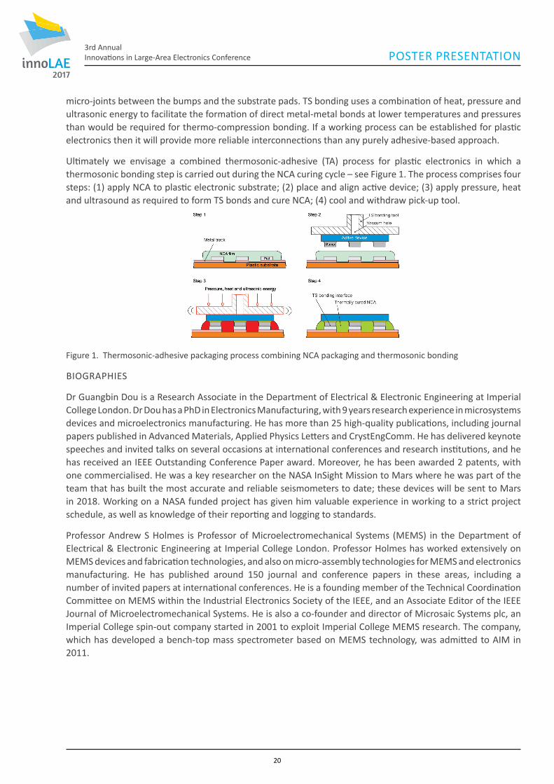
2017
3rd AnnualInnovations in Large-Area Electronics Conference POSTER PRESENTATION
micro-joints between the bumps and the substrate pads. TS bonding uses a combination of heat, pressure and ultrasonic energy to facilitate the formation of direct metal-metal bonds at lower temperatures and pressures than would be required for thermo-compression bonding. If a working process can be established for plastic electronics then it will provide more reliable interconnections than any purely adhesive-based approach.
Ultimately we envisage a combined thermosonic-adhesive (TA) process for plastic electronics in which a thermosonic bonding step is carried out during the NCA curing cycle – see Figure 1. The process comprises four steps: (1) apply NCA to plastic electronic substrate; (2) place and align active device; (3) apply pressure, heat and ultrasound as required to form TS bonds and cure NCA; (4) cool and withdraw pick-up tool.
Figure 1. Thermosonic-adhesive packaging process combining NCA packaging and thermosonic bonding
BIOGRAPHIES
Dr Guangbin Dou is a Research Associate in the Department of Electrical & Electronic Engineering at Imperial College London. Dr Dou has a PhD in Electronics Manufacturing, with 9 years research experience in microsystems devices and microelectronics manufacturing. He has more than 25 high-quality publications, including journal papers published in Advanced Materials, Applied Physics Letters and CrystEngComm. He has delivered keynote speeches and invited talks on several occasions at international conferences and research institutions, and he has received an IEEE Outstanding Conference Paper award. Moreover, he has been awarded 2 patents, with one commercialised. He was a key researcher on the NASA InSight Mission to Mars where he was part of the team that has built the most accurate and reliable seismometers to date; these devices will be sent to Mars in 2018. Working on a NASA funded project has given him valuable experience in working to a strict project schedule, as well as knowledge of their reporting and logging to standards.
Professor Andrew S Holmes is Professor of Microelectromechanical Systems (MEMS) in the Department of Electrical & Electronic Engineering at Imperial College London. Professor Holmes has worked extensively on MEMS devices and fabrication technologies, and also on micro-assembly technologies for MEMS and electronics manufacturing. He has published around 150 journal and conference papers in these areas, including a number of invited papers at international conferences. He is a founding member of the Technical Coordination Committee on MEMS within the Industrial Electronics Society of the IEEE, and an Associate Editor of the IEEE Journal of Microelectromechanical Systems. He is also a co-founder and director of Microsaic Systems plc, an Imperial College spin-out company started in 2001 to exploit Imperial College MEMS research. The company, which has developed a bench-top mass spectrometer based on MEMS technology, was admitted to AIM in 2011.
20
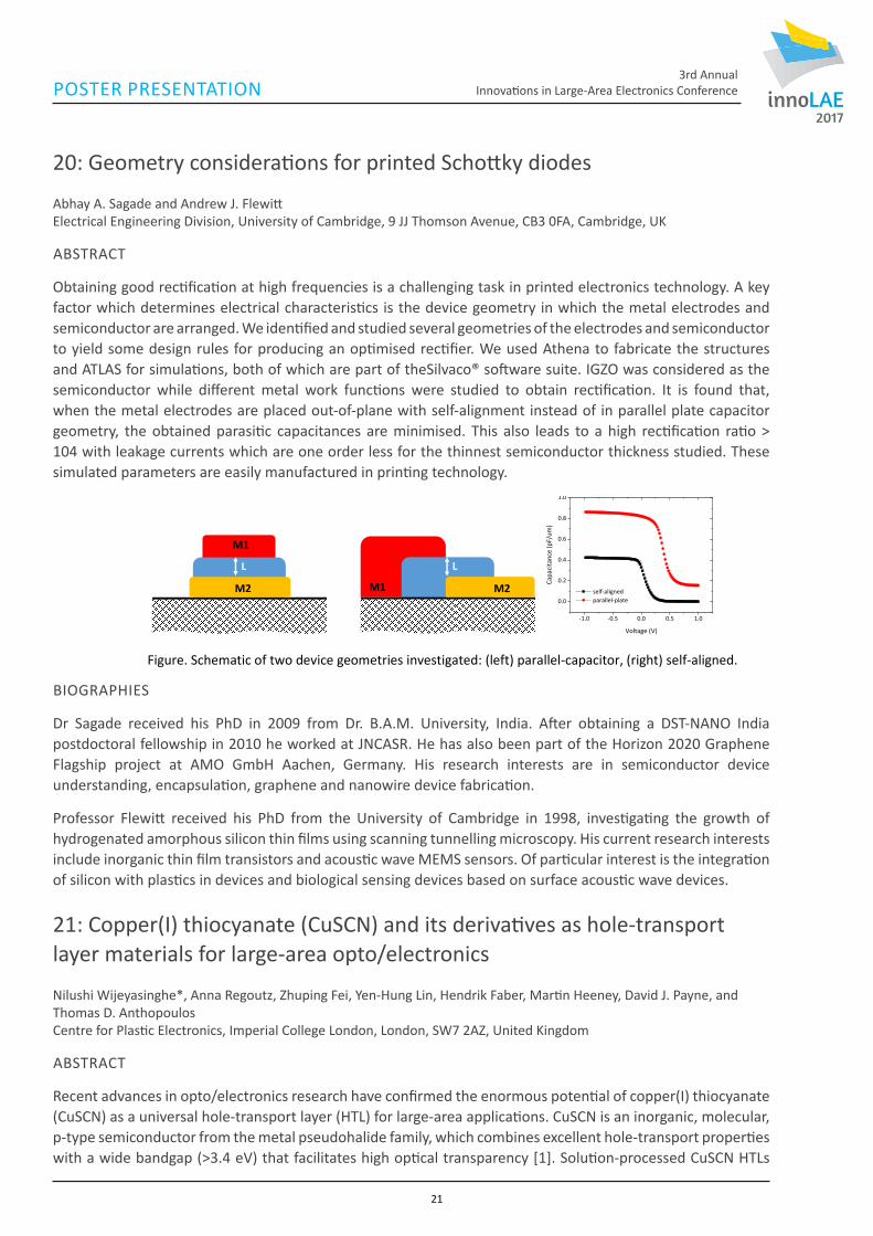
2017
3rd AnnualInnovations in Large-Area Electronics ConferencePOSTER PRESENTATION
20: Geometry considerations for printed Schottky diodes
Abhay A. Sagade and Andrew J. Flewitt Electrical Engineering Division, University of Cambridge, 9 JJ Thomson Avenue, CB3 0FA, Cambridge, UK
ABSTRACT
Obtaining good rectification at high frequencies is a challenging task in printed electronics technology. A key factor which determines electrical characteristics is the device geometry in which the metal electrodes and semiconductor are arranged. We identified and studied several geometries of the electrodes and semiconductor to yield some design rules for producing an optimised rectifier. We used Athena to fabricate the structures and ATLAS for simulations, both of which are part of theSilvaco® software suite. IGZO was considered as the semiconductor while different metal work functions were studied to obtain rectification. It is found that, when the metal electrodes are placed out-of-plane with self-alignment instead of in parallel plate capacitor geometry, the obtained parasitic capacitances are minimised. This also leads to a high rectification ratio > 104 with leakage currents which are one order less for the thinnest semiconductor thickness studied. These simulated parameters are easily manufactured in printing technology.
BIOGRAPHIES
Dr Sagade received his PhD in 2009 from Dr. B.A.M. University, India. After obtaining a DST-NANO India postdoctoral fellowship in 2010 he worked at JNCASR. He has also been part of the Horizon 2020 Graphene Flagship project at AMO GmbH Aachen, Germany. His research interests are in semiconductor device understanding, encapsulation, graphene and nanowire device fabrication.
Professor Flewitt received his PhD from the University of Cambridge in 1998, investigating the growth of hydrogenated amorphous silicon thin films using scanning tunnelling microscopy. His current research interests include inorganic thin film transistors and acoustic wave MEMS sensors. Of particular interest is the integration of silicon with plastics in devices and biological sensing devices based on surface acoustic wave devices.
Geometry considerations for printed Schottky diodes
Abhay A. Sagade and Andrew J. Flewitt
Electrical Engineering Division, University of Cambridge, 9 JJ Thomson Avenue, CB3 0FA, Cambridge, UK
E-mail: [email protected], [email protected]
Abstract:
Obtaining good rectification at high frequencies is a challenging task in printed electronics technology. A key factor which determines electrical characteristics is the device geometry in which the metal electrodes and semiconductor are arranged. We identified and studied several geometries of the electrodes and semiconductor to yield some design rules for producing an optimised rectifier. We used Athena to fabricate the structures and ATLAS for simulations, both of which are part of theSilvaco® software suite. IGZO was considered as the semiconductor while different metal work functions were studied to obtain rectification. It is found that, when the metal electrodes are placed out-of-plane with self-alignment instead of in parallel plate capacitor geometry, the obtained parasitic capacitances are minimised. This also leads to a high rectification ratio > 104 with leakage currents which are one order less for the thinnest semiconductor thickness studied. These simulated parameters are easily manufactured in printing technology.
-1.0 -0.5 0.0 0.5 1.0
0.0
0.2
0.4
0.6
0.8
1.0
self-aligned parallel-plate
Capa
citan
ce (p
F/um
)
Voltage (V)
Figure. Schematic of two device geometries investigated: (left) parallel-capacitor, (right) self-aligned.
Biography:
Dr Sagade received his PhD in 2009 from Dr. B.A.M. University, India. After obtaining a DST-NANO India postdoctoral fellowship in 2010 he worked at JNCASR. He has also been part of the Horizon 2020 Graphene Flagship project at AMO GmbH Aachen, Germany. His research interests are in semiconductor device understanding, encapsulation, graphene and nanowire device fabrication.
Professor Flewitt received his PhD from the University of Cambridge in 1998, investigating the growth of hydrogenated amorphous silicon thin films using scanning tunnelling microscopy. His current research interests include inorganic thin film transistors and acoustic wave MEMS sensors. Of particular interest is the integration of silicon with plastics in devices and biological sensing devices based on surface acoustic wave devices.
L
Device 1
M1 M2
Suitable for material with good conductivityMinimal stray capacitance
L
Device 3
M1
M2
Suitable for material with low conductivityLarge stray capacitance
Device 2
M1 M2
Suitable for any material conductivityOptimal stray capacitance
L L
Device 1
M1 M2
Suitable for material with good conductivityMinimal stray capacitance
L
Device 3
M1
M2
Suitable for material with low conductivityLarge stray capacitance
Device 2
M1 M2
Suitable for any material conductivityOptimal stray capacitance
L
21: Copper(I) thiocyanate (CuSCN) and its derivatives as hole-transport layer materials for large-area opto/electronics
Nilushi Wijeyasinghe*, Anna Regoutz, Zhuping Fei, Yen-Hung Lin, Hendrik Faber, Martin Heeney, David J. Payne, and Thomas D. Anthopoulos Centre for Plastic Electronics, Imperial College London, London, SW7 2AZ, United Kingdom
ABSTRACT
Recent advances in opto/electronics research have confirmed the enormous potential of copper(I) thiocyanate (CuSCN) as a universal hole-transport layer (HTL) for large-area applications. CuSCN is an inorganic, molecular, p-type semiconductor from the metal pseudohalide family, which combines excellent hole-transport properties with a wide bandgap (>3.4 eV) that facilitates high optical transparency [1]. Solution-processed CuSCN HTLs
21

2017
3rd AnnualInnovations in Large-Area Electronics Conference POSTER PRESENTATION
have been demonstrated in perovskite-based solar cells, organic photovoltaic (OPV) cells, organic light-emitting diodes (OLEDs) and thin-film transistors (TFTs) [2]. CuSCN exhibits greater chemical stability relative to the acidic PEDOT:PSS [3] and is a low-cost alternative to Spiro-MeOTAD – materials employed as conventional HTLs in the literature. Therefore, this unique combination of attractive characteristics makes CuSCN an ideal HTL candidate for large-area applications.
Here we report on the optimisation of low temperature, solution-processed CuSCN-based HTLs, and present a novel derivative of CuSCN with similar hole-transport properties. First, the conductivity and Fermi level of CuSCN is modified with the addition of chemical p-dopants, and field-effect hole mobilities exceeding twice that of pristine CuSCN are observed in the optimised doped systems. Next, novel solution-processing schemes for CuSCN are explored, and alternatives to the standard n-alkyl sulphide solvents are demonstrated. These novel formulations were utilised to spin-cast CuSCN HTLs with superior field-effect hole mobilities (~0.1 cm2V–1s–1) and high uniformity over large-area substrates. The environmental stability of CuSCN HTLs and their suitability for ambient air solution-processing are also assessed. Finally, the synthesis of a novel wide bandgap semiconductor from the metal pseudohalide family is reported and a comprehensive investigation into its suitability as a next-generation HTL is presented. HTL deposition parameters are optimised using TFT measurements and a range of thin-film analysis techniques, such as AFM and XPS. Consequently, the tremendous potential of this family of inorganic compounds to replace conventional organic HTL materials is demonstrated.
[1] P. Pattanasattayavong, et al., Adv. Mater., 25, 1504, 2013. [2] N. Wijeyasinghe & T.D. Anthopoulos, Semicond. Sci. Technol., 30, 104002, 2015. [3] A. Garcia, et al., Adv. Mater., 24, 5368, 2012.
BIOGRAPHY
Nilushi is a PhD candidate in the Centre for Plastic Electronics at Imperial College London. As the recipient of an EPSRC DTA funding award, she conducts research in Experimental Solid State (EXSS) Physics under the supervision of Professor Thomas Anthopoulos. She completed her undergraduate degree in Physics at University College London, where she also received the Corrigan Prize for experimental work, and two EPSRC funding awards for summer projects in Condensed Matter and Materials Physics. Prior to joining Imperial, Nilushi graduated with a research MSc in Atomic and Laser Physics from the University of Oxford, where she collaborated with theoreticians at the University of Cambridge on a non-linear optics project. She was a committee member of the Society for Information Display (SID) UK & Ireland Chapter for 2014-16, and the postgraduate representative of the EXSS research group at Imperial for 2015-16.
22: Printing Carbon Nanotubes Using Large-Area Fine-Feature Printer
Qingshen Jing1, Michael Smith1, Yeonsik Choi1, Nicolo Chiodarelli2, Michael De Volder2, Sohini Kar-Narayan1 1Department of Material Science and Metallurgy, University of Cambridge, UK 2Institute for Manufacturing, Department of Engineering, University of Cambridge, UK.
ABSTRACT
Carbon nanotubes (CNTs) have been proved promising as additives in battery electrodes, super capacitors and other electronics such as flexible or stretchable devices. Ways of making uniform CNT thin films have been mature and economic. Meanwhile, complex and fine pattern of CNT electrodes are desired to fulfil more complicated functions. Technologies of using a commercial printer to inkjet water/oil dispersed CNT solutions have been attempted however are hampered due to narrow range of solution viscosity permitted by printers.
Large-area fine-feature aerosol printer is a high-resolution rapid-prototyping equipment suitable for printing up electronic circuit with a widely ranged compatibility of ink materials, including conductive nanoparticles, polymers, insulators, adhesives, etchants, etc., with a work area as large as 175 mm x 200 mm.
22
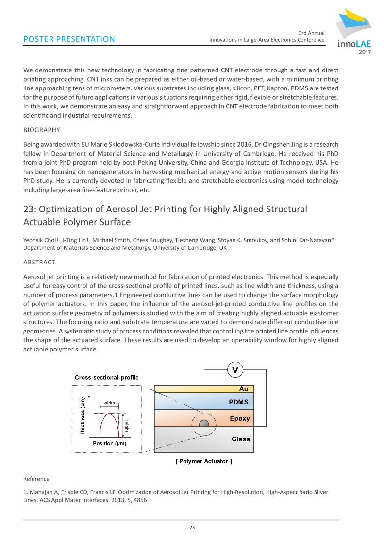
2017
3rd AnnualInnovations in Large-Area Electronics ConferencePOSTER PRESENTATION
We demonstrate this new technology in fabricating fine patterned CNT electrode through a fast and direct printing approaching. CNT inks can be prepared as either oil-based or water-based, with a minimum printing line approaching tens of micrometers. Various substrates including glass, silicon, PET, Kapton, PDMS are tested for the purpose of future applications in various situations requiring either rigid, flexible or stretchable features. In this work, we demonstrate an easy and straightforward approach in CNT electrode fabrication to meet both scientific and industrial requirements.
BIOGRAPHY
Being awarded with EU Marie Skłodowska-Curie individual fellowship since 2016, Dr Qingshen Jing is a research fellow in Department of Material Science and Metallurgy in University of Cambridge. He received his PhD from a joint PhD program held by both Peking University, China and Georgia Institute of Technology, USA. He has been focusing on nanogenerators in harvesting mechanical energy and active motion sensors during his PhD study. He is currently devoted in fabricating flexible and stretchable electronics using model technology including large-area fine-feature printer, etc.
23: Optimization of Aerosol Jet Printing for Highly Aligned Structural Actuable Polymer Surface
Yeonsik Choi†, I-Ting Lin†, Michael Smith, Chess Boughey, Tiesheng Wang, Stoyan K. Smoukov, and Sohini Kar-Narayan* Department of Materials Science and Metallurgy, University of Cambridge, UK
ABSTRACT
Aerosol jet printing is a relatively new method for fabrication of printed electronics. This method is especially useful for easy control of the cross-sectional profile of printed lines, such as line width and thickness, using a number of process parameters.1 Engineered conductive lines can be used to change the surface morphology of polymer actuators. In this paper, the influence of the aerosol-jet-printed conductive line profiles on the actuation surface geometry of polymers is studied with the aim of creating highly aligned actuable elastomer structures. The focusing ratio and substrate temperature are varied to demonstrate different conductive line geometries. A systematic study of process conditions revealed that controlling the printed line profile influences the shape of the actuated surface. These results are used to develop an operability window for highly aligned actuable polymer surface.
Reference
1. Mahajan A, Frisbie CD, Francis LF. Optimization of Aerosol Jet Printing for High-Resolution, High-Aspect Ratio Silver Lines. ACS Appl Mater Interfaces. 2013, 5, 4856
Optimization of Aerosol Jet Printing for Highly Aligned Structural Actuable Polymer Surface
Yeonsik Choi†, I-Ting Lin†, Michael Smith, Chess Boughey, Tiesheng Wang,
Stoyan K. Smoukov, and Sohini Kar-Narayan*
Department of Materials Science and Metallurgy, University of Cambridge, UK Abstract Aerosol jet printing is a relatively new method for fabrication of printed electronics. This method is especially useful for easy control of the cross-sectional profile of printed lines, such as line width and thickness, using a number of process parameters.1 Engineered conductive lines can be used to change the surface morphology of polymer actuators. In this paper, the influence of the aerosol-jet-printed conductive line profiles on the actuation surface geometry of polymers is studied with the aim of creating highly aligned actuable elastomer structures. The focusing ratio and substrate temperature are varied to demonstrate different conductive line geometries. A systematic study of process conditions revealed that controlling the printed line profile influences the shape of the actuated surface. These results are used to develop an operability window for highly aligned actuable polymer surface.
Reference
1. Mahajan A, Frisbie CD, Francis LF. Optimization of Aerosol Jet Printing for High-Resolution, High-Aspect Ratio Silver Lines. ACS Appl Mater Interfaces. 2013, 5, 4856
Keywords: Aerosol jet printing, Soft electronics, Actuator, Process optimization
23
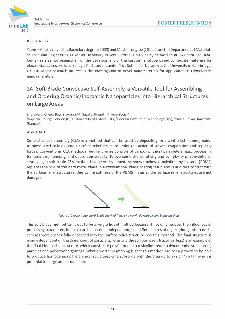
2017
3rd AnnualInnovations in Large-Area Electronics Conference POSTER PRESENTATION
24: Soft-Blade Convective Self-Assembly, a Versatile Tool for Assembling and Ordering Organic/Inorganic Nanoparticles into Hierarchical Structures on Large Areas
Shengyang Chen1, Paul Stavrinou1,2, Natalie Stingelin1,3, Ioan Botiz1,4
1Imperial College London (UK); 2University of Oxford (UK); 3Georgia Institute of Technology (US); 4Babes-Bolyai University (Romania)
ABSTRACT
Convective self-assembly (CSA) is a method that can be used by depositing, in a controlled manner, nano- to micro-sized colloids onto a surface relief structure under the action of solvent evaporation and capillary forces. Conventional CSA methods require precise controls of various physical parameters, e.g., processing temperature, humidity, and deposition velocity. To overcome the sensitivity and complexity of conventional strategies, a soft-blade CSA method has been developed. As shown below, a polydimethylsiloxane (PDMS) replaces the role of the hard metal blade in a conventional blade-coating setup and is in direct contact with the surface relief structures. Due to the softness of the PDMS material, the surface relief structures are not damaged.
Figure 1 Conventional hard-blade method (left) and newly developed soft-blade method.
This soft-blade method turns out to be a very efficient method because it not only reduces the influences of processing parameters but also can be material-independent, i.e., different sizes of organic/inorganic material spheres were successfully deposited into the surface relief structures via this method. The final structure is mainly dependent on the dimensions of particle spheres and the surface relief structures. Fig.2 is an example of the final hierarchical structure, which consists of polyfluorene-co-divinylbenzene (polymer emissive material) particles and polystyrene gratings. What’s worth mentioning is that this method has been proved to be able to produce homogeneous hierarchical structures on a substrate with the area up to 2x2 cm2 so far, which is potential for large area production.
BIOGRAPHY
Yeonsik Choi received his Bachelors degree (2009) and Masters degree (2011) from the Department of Materials Science and Engineering at Yonsei University in Seoul, Korea. Up to 2015, he worked at LG Chem. Ltd. R&D Center as a senior researcher for the development of the carbon nanotube based composite materials for electronic devices. He is currently a PhD student under Prof. Sohini Kar-Narayan at the University of Cambridge, UK. His Major research interest is the investigation of novel nanomaterials for application in triboelectric nanogenerators.
24
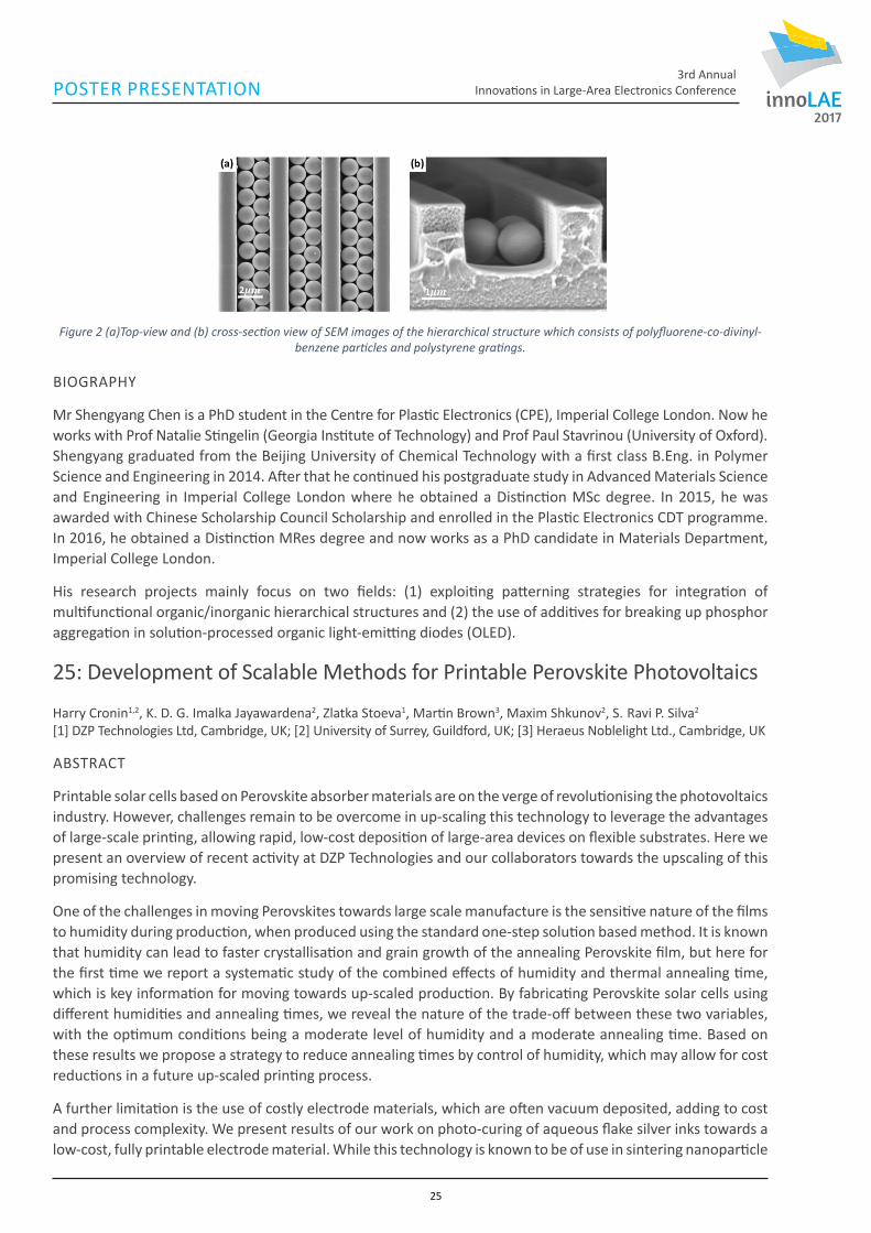
2017
3rd AnnualInnovations in Large-Area Electronics ConferencePOSTER PRESENTATION
Figure 2 (a)Top-view and (b) cross-section view of SEM images of the hierarchical structure which consists of polyfluorene-co-divinyl-benzene particles and polystyrene gratings.
BIOGRAPHY
Mr Shengyang Chen is a PhD student in the Centre for Plastic Electronics (CPE), Imperial College London. Now he works with Prof Natalie Stingelin (Georgia Institute of Technology) and Prof Paul Stavrinou (University of Oxford).Shengyang graduated from the Beijing University of Chemical Technology with a first class B.Eng. in Polymer Science and Engineering in 2014. After that he continued his postgraduate study in Advanced Materials Science and Engineering in Imperial College London where he obtained a Distinction MSc degree. In 2015, he was awarded with Chinese Scholarship Council Scholarship and enrolled in the Plastic Electronics CDT programme. In 2016, he obtained a Distinction MRes degree and now works as a PhD candidate in Materials Department, Imperial College London.
His research projects mainly focus on two fields: (1) exploiting patterning strategies for integration of multifunctional organic/inorganic hierarchical structures and (2) the use of additives for breaking up phosphor aggregation in solution-processed organic light-emitting diodes (OLED).
25: Development of Scalable Methods for Printable Perovskite Photovoltaics
Harry Cronin1,2, K. D. G. Imalka Jayawardena2, Zlatka Stoeva1, Martin Brown3, Maxim Shkunov2, S. Ravi P. Silva2
[1] DZP Technologies Ltd, Cambridge, UK; [2] University of Surrey, Guildford, UK; [3] Heraeus Noblelight Ltd., Cambridge, UK
ABSTRACT
Printable solar cells based on Perovskite absorber materials are on the verge of revolutionising the photovoltaics industry. However, challenges remain to be overcome in up-scaling this technology to leverage the advantages of large-scale printing, allowing rapid, low-cost deposition of large-area devices on flexible substrates. Here we present an overview of recent activity at DZP Technologies and our collaborators towards the upscaling of this promising technology.
One of the challenges in moving Perovskites towards large scale manufacture is the sensitive nature of the films to humidity during production, when produced using the standard one-step solution based method. It is known that humidity can lead to faster crystallisation and grain growth of the annealing Perovskite film, but here for the first time we report a systematic study of the combined effects of humidity and thermal annealing time, which is key information for moving towards up-scaled production. By fabricating Perovskite solar cells using different humidities and annealing times, we reveal the nature of the trade-off between these two variables, with the optimum conditions being a moderate level of humidity and a moderate annealing time. Based on these results we propose a strategy to reduce annealing times by control of humidity, which may allow for cost reductions in a future up-scaled printing process.
A further limitation is the use of costly electrode materials, which are often vacuum deposited, adding to cost and process complexity. We present results of our work on photo-curing of aqueous flake silver inks towards a low-cost, fully printable electrode material. While this technology is known to be of use in sintering nanoparticle
25
2017
3rd AnnualInnovations in Large-Area Electronics Conference POSTER PRESENTATION
based systems, which benefit from significant melting point suppression compared with bulk material, larger flake inks are more challenging to sinter by this means owing to the higher required temperatures. We find that with photo-curing the conductivity of such inks approaches and in some cases matches that of typical nanoparticle inks. Furthermore, in an application employing screen printed silver lines, the yield of conductive patterns was increased from 46% untreated to 90% after photo-curing.
Finally we present initial results of Perovskite materials manufactured by a non-standard powder-based method, and a readily scalable slot-die printing process based on a blend of this material with various photo-active polymers. These initial results demonstrate the suitability of this method for upscaling and serve as a promising basis for future research.
BIOGRAPHY
Harry Cronin is an EngD research engineer working jointly at DZP Technologies in Cambridge and the University of Surrey. Harry received his MSci in Physics from Imperial College London and started his doctoral research in 2013. His research is focused on materials and process development for printed electronics, with a focus on printed solar cells.
26: Design of Metaferrites using Genetic Algorithms and Other Optimisation Techniques
By Philip Beal, QMUL EECS
ABSTRACT
Metaferrites are a class of metamaterials designed for the purpose of replicating the electrical properties of ferrite materials without actually using any, which could in some cases disrupt the function of devices due to the material’s other properties. Additionally, metaferrites are customisable, allowing for bespoke materials with properties difficult or impossible to produce otherwise.
This work seeks to design novel metaferrites using a combination of genetic algorithms, machine learning and other optimisation techniques. If possible, it also seeks to construct a database of structures that will speed further endeavours in the area by quickly identifying which features correspond to a given set of parameters. So far, development of the design programs has been the primary output, with fabrication expected to be possible in the near future
BIOGRAPHY
Philip Beal is a PhD student studying Electronic Engineering at Queen Mary University of London under the supervision of Professor Yang Hao and Dr Khalid Rajab.
27: Magnetoelectronics on Bendable Ultra-Thin Si Chips
Hadi Heidari, Fengyan Liu and Ravinder Dahiya Bendable Electronics and Sensing Technologies (BEST) Group, University of Glasgow, Glasgow, UK
ABSTRACT
The integration of magnetic elements into electronic devices, often referred to as magnetoelectronics, is an interesting development in flexible electronics. Here we present magentic devices (e.g. Hall Sensor and Giant Magnetoresistance (GMR)) on ultra-thin chips and our investigation realted to the effects of bending stress on these devices. The bending induced variations in device parameters are needed to improve device models and design the new generation of flexible magnetic sensors. We have recently presented the ending-induced stress
26
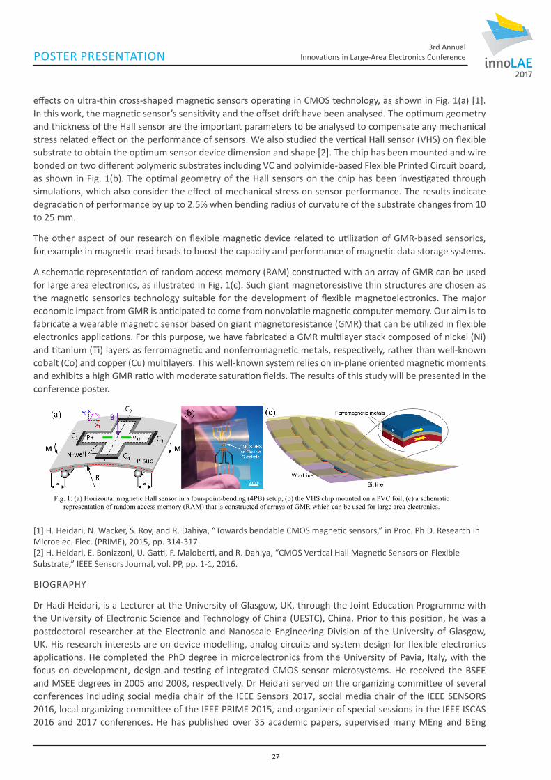
2017
3rd AnnualInnovations in Large-Area Electronics ConferencePOSTER PRESENTATION
effects on ultra-thin cross-shaped magnetic sensors operating in CMOS technology, as shown in Fig. 1(a) [1]. In this work, the magnetic sensor’s sensitivity and the offset drift have been analysed. The optimum geometry and thickness of the Hall sensor are the important parameters to be analysed to compensate any mechanical stress related effect on the performance of sensors. We also studied the vertical Hall sensor (VHS) on flexible substrate to obtain the optimum sensor device dimension and shape [2]. The chip has been mounted and wire bonded on two different polymeric substrates including VC and polyimide-based Flexible Printed Circuit board, as shown in Fig. 1(b). The optimal geometry of the Hall sensors on the chip has been investigated through simulations, which also consider the effect of mechanical stress on sensor performance. The results indicate degradation of performance by up to 2.5% when bending radius of curvature of the substrate changes from 10 to 25 mm.
The other aspect of our research on flexible magnetic device related to utilization of GMR-based sensorics, for example in magnetic read heads to boost the capacity and performance of magnetic data storage systems.
A schematic representation of random access memory (RAM) constructed with an array of GMR can be used for large area electronics, as illustrated in Fig. 1(c). Such giant magnetoresistive thin structures are chosen as the magnetic sensorics technology suitable for the development of flexible magnetoelectronics. The major economic impact from GMR is anticipated to come from nonvolatile magnetic computer memory. Our aim is to fabricate a wearable magnetic sensor based on giant magnetoresistance (GMR) that can be utilized in flexible electronics applications. For this purpose, we have fabricated a GMR multilayer stack composed of nickel (Ni) and titanium (Ti) layers as ferromagnetic and nonferromagnetic metals, respectively, rather than well-known cobalt (Co) and copper (Cu) multilayers. This well-known system relies on in-plane oriented magnetic moments and exhibits a high GMR ratio with moderate saturation fields. The results of this study will be presented in the conference poster.
[1] H. Heidari, N. Wacker, S. Roy, and R. Dahiya, “Towards bendable CMOS magnetic sensors,” in Proc. Ph.D. Research in Microelec. Elec. (PRIME), 2015, pp. 314-317. [2] H. Heidari, E. Bonizzoni, U. Gatti, F. Maloberti, and R. Dahiya, “CMOS Vertical Hall Magnetic Sensors on Flexible Substrate,” IEEE Sensors Journal, vol. PP, pp. 1-1, 2016.
BIOGRAPHY
Dr Hadi Heidari, is a Lecturer at the University of Glasgow, UK, through the Joint Education Programme with the University of Electronic Science and Technology of China (UESTC), China. Prior to this position, he was a postdoctoral researcher at the Electronic and Nanoscale Engineering Division of the University of Glasgow, UK. His research interests are on device modelling, analog circuits and system design for flexible electronics applications. He completed the PhD degree in microelectronics from the University of Pavia, Italy, with the focus on development, design and testing of integrated CMOS sensor microsystems. He received the BSEE and MSEE degrees in 2005 and 2008, respectively. Dr Heidari served on the organizing committee of several conferences including social media chair of the IEEE Sensors 2017, social media chair of the IEEE SENSORS 2016, local organizing committee of the IEEE PRIME 2015, and organizer of special sessions in the IEEE ISCAS 2016 and 2017 conferences. He has published over 35 academic papers, supervised many MEng and BEng
Magnetoelectronics on Bendable Ultra-Thin Si Chips Hadi Heidari, Fengyan Liu and Ravinder Dahiya
Bendable Electronics and Sensing Technologies (BEST) Group, University of Glasgow, Glasgow, UK The integration of magnetic elements into electronic devices, often referred to as magnetoelectronics, is an interesting development in flexible electronics. Here we present magentic devices (e.g. Hall Sensor and Giant Magnetoresistance (GMR)) on ultra-thin chips and our investigation realted to the effects of bending stress on these devices. The bending induced variations in device parameters are needed to improve device models and design the new generation of flexible magnetic sensors. We have recently presented the bending-induced stress effects on ultra-thin cross-shaped magnetic sensors operating in CMOS technology, as shown in Fig. 1(a) [1]. In this work, the magnetic sensor’s sensitivity and the offset drift have been analysed. The optimum geometry and thickness of the Hall sensor are the important parameters to be analysed to compensate any mechanical stress related effect on the performance of sensors. We also studied the vertical Hall sensor (VHS) on flexible substrate to obtain the optimum sensor device dimension and shape [2]. The chip has been mounted and wire bonded on two different polymeric substrates including PVC and polyimide-based Flexible Printed Circuit board, as shown in Fig. 1(b). The optimal geometry of the Hall sensors on the chip has been investigated through simulations, which also consider the effect of mechanical stress on sensor performance. The results indicate degradation of performance by up to 2.5% when bending radius of curvature of the substrate changes from 10 to 25 mm. The other aspect of our research on flexible magnetic device related to utilization of GMR-based sensorics, for example in magnetic read heads to boost the capacity and performance of magnetic data storage systems. A schematic representation of random access memory (RAM) constructed with an array of GMR can be used for large area electronics, as illustrated in Fig. 1(c). Such giant magnetoresistive thin structures are chosen as the magnetic sensorics technology suitable for the development of flexible magnetoelectronics. The major economic impact from GMR is anticipated to come from nonvolatile magnetic computer memory. Our aim is to fabricate a wearable magnetic sensor based on giant magnetoresistance (GMR) that can be utilized in flexible electronics applications. For this purpose, we have fabricated a GMR multilayer stack composed of nickel (Ni) and titanium (Ti) layers as ferromagnetic and nonferromagnetic metals, respectively, rather than well-known cobalt (Co) and copper (Cu) multilayers. This well-known system relies on in-plane oriented magnetic moments and exhibits a high GMR ratio with moderate saturation fields. The results of this study will be presented in the conference poster.
[1] H. Heidari, N. Wacker, S. Roy, and R. Dahiya, "Towards bendable CMOS magnetic sensors," in Proc. Ph.D. Research in Microelec. Elec. (PRIME), 2015, pp. 314-317. [2] H. Heidari, E. Bonizzoni, U. Gatti, F. Maloberti, and R. Dahiya, "CMOS Vertical Hall Magnetic Sensors on Flexible Substrate," IEEE Sensors Journal, vol. PP, pp. 1-1, 2016.
Fig. 1: (a) Horizontal magnetic Hall sensor in a four-point-bending (4PB) setup, (b) the VHS chip mounted on a PVC foil, (c) a schematic
representation of random access memory (RAM) that is constructed of arrays of GMR which can be used for large area electronics.
27
2017
3rd AnnualInnovations in Large-Area Electronics Conference POSTER PRESENTATION
students, and acts as a reviewer for several journals and conferences. He received different paper awards at the IEEE ISCAS 2014, IEEE PRIME 2014, and the ISSCC 2016 conferences. He was a visiting scholar with the University of Macau, China, and McGill University, Canada.
28: Low-voltage electrospinning patterning of functional micro- and nano-fibres
Xia Li1,2, Guokun Ma1, Wenyu Wang1, and Yan Yan Shery Huang1 1. Engineering Dept, University of Cambridge Trumpington St, Cambridge CB2 1PZ 2. Cavendish Laboratory, University of Cambridge, J J Thomson Avenue Cambridge CB3 0HE
ABSTRACT
Applications of micro-nano fibrous structures are vital to a number of emerging technologies such as fibre-based sensors, filtration membranes, batteries, energy storage and a range of bioengineering technologies such as tissue scaffold implants, drug delivery and wound dressing. Electrospinning is a versatile technique for the construction of microfibrous and nanofibrous structures with considerable potential in the applications mentioned above. In the simplest form, electrospinning uses a high voltage of tens of thousands volts to draw ultra-fine polymer fibres over a large distance. However, the high voltage limits the flexible combination of material selection, deposition substrate, and control of patterns. Extending the capability of electrospinning, our work demonstrates a new ultra-low voltage continuous electrospinning patterning (LEP) technique. LEP utilizes solution dependent ‘initiators’, which reduces the applied voltage threshold to as low as 50 V, simultaneously permitting continuous fibre patterning. By incorporating with a microfluidic-based spinneret, LEP extends its applications in printing high performance conductive lines onto plastic substrates at mild temperatures. Compared to published literature using other printing techniques, the LEP patterned silver lines demonstrate improved aspect ratios for single pass lines. Post 90 °C heat treatment, the resulted silver lines show a conductivity value one order of magnitude smaller than its bulk counterpart, which is of comparable performance to other reported work requiring thermal treatments at temperatures exceeding 100 °C. In summary, the LEP technique reported here should open up new avenues in the patterning of bio-/ electronic- elements, and free-form nano- to micro-scale fibrous structures with a versatile range of materials, broadening the application scope of room temperature, solution-based direct-write fabrication techniques.
Acknowledgement
Thanks for the assistance from Yuan Yuan Hu and Lang Jiang from Cavendish Laboratory in performing the experiment.
BIOGRAPHY
Wenyu Wang acquired his Bachelor’s degree in mechanical engineering from Tsinghua University (Beijing) in 2016, and then started a Ph.D. study at the University of Cambridge, focusing on biofabrication. His supervisor is Dr. Shery Huang. Wenyu has participated several research projects during his undergraduate period, ranging from precise processing of turbine blade to construction of a stereolithographic 3D printer, and has co-authored two EI articles. Now his research focuses on improving the functionality of additive manufacturing methods to enlarge the applications of the final products, like soft electronics and biocompatible device.
29: Monolayer graphene membrane device for bio-sensing applications
R. K. Guptaa, U. Monteverdea, Omar. M. Dawooda,d, F. Hadia, J. Campbella, J. Sextona, L. Majewskia, M. Missousa, Dean Jacksone, Robert J. Youngd, M. Miglioratoa, Neil Dixonb,c
aSchool of Electrical & Electronic Engineering, bManchester Institute of Biotechnology, cSchool of Chemistry, dSchool of Materials, eFaculty of Biology, Medicine and Health The University of Manchester, Manchester, M13 9PL, UK
28

2017
3rd AnnualInnovations in Large-Area Electronics ConferencePOSTER PRESENTATION
ABSTRACT
Single layer graphene, owing to its extraordinary electronic and chemical properties, offers the potential application for the fabrication of an ultra-sensitive biosensor and/or chemisensor [1]. Free standing (suspended) graphene sheet have shown high charge carriers mobility and large surface area for bio-or chemical interaction/interface as compared to similar sized substrate supported graphene sheet [2,3]. Recently reported micron size free standing graphene beam based two terminal biosensors have achieved sensitive multiplexed detection of lung cancer tumor markers [4]. Graphene channel based three terminal devices - graphene field effect transistor (GFET), even with the limitations of low Ion/Ioff ratio, exhibits characteristic parameter; charge neutrality voltage (VCN), which is very sensitive to the surface charge interacting with graphene channel. The charge sensing ability of suspended graphene based FET (SGFET) can be explored for an ultra-sensitive biosensor for biomarkers and pathogens in their physiological conditions or in an environment.
In this poster, we shall be showing the improved device structure and electrical results of an array based three terminal free-standing graphene devices (Fig. 1), in which graphene is suspended over micro-meter scale cavities with top and back gate contacts. The device uses conventional lithography and graphene transfer process for device fabrication. The end applications of this device shall be explored for an ultra-sensitive detection of DNA hybridisation and/or cardiac proteins.
References
[1] S. P. Lonkar, et. al, Nano Research, vol. 8, pp. 1039-1074, Apr 2015. [2] K. I. Bolotin, et al., vol. 146, pp. 351-355, 2008. [3] Z. Cheng, et. al, Nano Lett, vol. 10, pp. 1864-8, May 12 2010. [4] P. Li, et. al, Biosensors and Bioelectronics, vol. 72, pp. 168-174, 2015.
BIOGRAPHY
Rakesh obtained a Master’s degree in Electronics from the University of Jammu, J&K, India, in 2002; later he received his MPhil degree in Micro and Nanotechnology from University of Cambridge, UK, in 2010. He had been a visiting research scholar at the Center for Nanotechnology and Astrobiology, NASA Ames research center, CA, USA, for 2013-14. There he was involved in the designing and testing of nano-biosensors for Astronaut’s cardiac health monitoring.
In September 2015, Rakesh won the President Doctoral Scholar Award and is currently pursuing his doctoral research work on the fabrication of graphene membranes-based biosensors for an ultra-sensitive detection of biomarkers, in School of Electrical and Electronics Engineering, The University of Manchester.
Fig. 1 Drain-Source current variations at different gate biasing (inset; Device cartoon)
29

2017
3rd AnnualInnovations in Large-Area Electronics Conference POSTER PRESENTATION
30: Interfacial Engineering for High-Efficiency Polymer: Fullerene Solar Cells with Improved Stability
Sungho Nam1,2, Jooyeok Seo2, Hyemi Han2, Hwajeong Kim2, Youngkyoo Kim*2, Donal D. C. Bradley*1,3 1 Department of Physics, Division of Mathematical, Physical and Life Sciences, University of Oxford, Oxford OX1 3PU, United Kingdom 2 Organic Nanoelectronics Laboratory, Department of Chemical Engineering, School of Applied Chemical Engineering, Kyungpook National University, Daegu 41566, Republic of Korea 3 Department of Engineering Science, Division of Mathematical, Physical and Life Sciences, University of Oxford, Oxford OX1 3PJ, United Kingdom
ABSTRACT
Polymer solar cells with polymer:fullerene bulk heterojunction (BHJ) layers have been spotlighted in the field of green energy and flexible electronics due to their potential for low-cost fabrication of flexible plastic solar modules by employing continuous roll-to-roll processes. The polymer:fullerene solar cells have recently exhibited ca. 12 % power conversion efficiency (PCE) by utilizing new electron-donating polymers through device engineering. In addition to the material aspects, interfacial engineering between the electron-collecting buffer layers and the organic photoactive layers by insertion of an organic dipole interlayer has been proposed as a simple and scalable way to improve the overall solar cell performance. Despite recent progress, however, module efficiency and operating stability are still inferior to inorganic solar cells in the market leaving the need for further development. This presentation will introduce new polymeric interlayers for high efficiency polymer solar cells and discuss their enhanced stability under continuous illumination with solar light.
Figure 1. (left-side) Chemical structure of polyacetylene-based polyelectrolyte material, cross-sectional transmission electron microscope (TEM) image of device and nitrogen-mapping Auger electron microscope (AEM) image of ZnO/PDEPB layers. (right-side) J-V curves of devices under 10 h continuous solar simulated light (100 mW/cm2) without (w/o)/with (w/) a UV-cutoff filter (UCF).
31: Spray-cast multilayer perovskite solar cells with an active-area of 1.5 cm2
James E. Bishop1 and David K. Mohamad1, Michael Stringer1, Kevin Bass2 and David G. Lidzey1* 1) Department of Physics & Astronomy, University of Sheffield, Hicks Building, Hounsfield Road, Sheffield, S3 7RH, U.K. 2) CREST, University of Loughborough, Holywell Park, Loughborough University Science and Enterprise Parks, LE11 3TU, U.K.
ABSTRACT
We utilise spray-coating under ambient conditions to sequentially deposit compact-TiO2, mesoporous-TiO2, CH3NH3PbI(3-x)Clx perovskite and doped spiro-OMeTAD layers, creating a mesoporous standard architecture perovskite solar cell (PSC). The devices created had an average power conversion efficiency (PCE) of 9.2% and a peak PCE of 10.2%; values that compare favourably with control-devices fabricated by spin-casting that had an average efficiency of 11.4 %. We show that our process can be used to create devices having an active-area of
30

2017
3rd AnnualInnovations in Large-Area Electronics ConferencePOSTER PRESENTATION
Spray-cast multilayer perovskite solar cells with an active-area of 1.5 cm2
James E. Bishop1 and David K. Mohamad1, Michael Stringer1,
Kevin Bass2 and David G. Lidzey1*
1) Department of Physics & Astronomy, University of Sheffield, Hicks Building, Hounsfield
Road, Sheffield, S3 7RH, U.K.
2) CREST, University of Loughborough, Holywell Park, Loughborough University Science and Enterprise Parks, LE11 3TU, U.K.
*Corresponding author, email [email protected]
Abstract
We utilise spray-coating under ambient conditions to sequentially deposit compact-TiO2,
mesoporous-TiO2, CH3NH3PbI(3-x)Clx perovskite and doped spiro-OMeTAD layers, creating
a mesoporous standard architecture perovskite solar cell (PSC). The devices created had an
average power conversion efficiency (PCE) of 9.2% and a peak PCE of 10.2%; values that
compare favourably with control-devices fabricated by spin-casting that had an average
efficiency of 11.4 %. We show that our process can be used to create devices having an
active-area of 1.5 cm2 having a certified efficiency of 6.6 %. This work demonstrates the
versatility of spray-coating as well as its potential as a method of manufacturing low-cost,
large-area, efficient perovskite devices.
1.5 cm2 having a certified efficiency of 6.6 %. This work demonstrates the versatility of spray-coating as well as its potential as a method of manufacturing low-cost, large-area, efficient perovskite devices.
BIOGRAPHY
James Bishop is a second year PhD student working under the supervision of Professor David Lidzey as a member of the Electronic and Photonic Molecular Materials (EPMM) group, based in the department of Physics and Astronomy, University of Sheffield. His research focuses on developing scalable manufacturing processes for perovskite based photovoltaics, with a particular focus on spray-coating as a means to deposit large area devices.
32: Spray coated zinc oxide for large area electronic applications
Tiago Carneiro Gomes1,2, Neri Alves2 and Jeff Kettle1
1Bangor University, Bangor, Wales, UK; 2UNESP, Univ Estadual Paulista, Presidente Prudente, SP, Brazil
ABSTRACT
The potential application for metal oxide semiconductors in large area electronic has increased owing to the possibility for manufacturing flexible, transparent and lightweight devices from simple deposition techniques such as spray coating, inkjet-printing, screen-printing or roll-to-roll. Control of process parameters including coating and annealing conditions is important to achieve optimal and reproducible device performance parameters.
Within this context the zinc oxide (ZnO) is well known metal oxide semiconductor that has great potential due to its high charge carrier mobility, high optical transmittance in the visible spectrum and relatively good mechanical flexibility. In addition, it can be formed from pyrolysis at a reasonably low temperatures (150 - 450ºC), by spray coating from organic precursors. In this presentation, the electrical, optical and morphologic properties of spray coating ZnO films produced from a solution of zinc acetate dehydrated in methoxyethanol will be discussed. The influence of processing parameters such as concentration and annealing conditions will be discussed. In addition, the influence of these parameters upon surface roughness and transmission properties will be reported. Finally, the electron mobility is evaluated from thin film transistors, with values of up to 10-1 cm2/V.s reproducibly reached.
BIOGRAPHY
Tiago Carneiro Gomes is PhD student in Materials Science & Technology from UNESP, Brazil. Currently, he is visiting researcher in Bangor University, Wales and supervised by Dr. Jeff Kettle. His work is focused on processing and stability of ZnO transistors for sensor applications. His experience include the fabrication of the devices such as organic transistors, MIS capacitors and metal-oxide transistors using printing methods such as inkjet printing and spray coating.
31

2017
3rd AnnualInnovations in Large-Area Electronics Conference POSTER PRESENTATION
33: Low-Cost Testing of Flexible Printed VLSI Prototypes
Jedrzej Kufel, ARM
ABSTRACT
Testing is one of the key challenges in the manufacturability of flexible and printed electronics. While reliability is a hot research topic, functional verification relies on methodologies well established in the silicon arena. Functional testing for plastic flexible chips however varies from cheap and simplistic breadboard prototyping to more expensive and sophisticated tester approach.
To develop testing capabilities for our PlasticARM flexible printed test chip we modified an off-the-shelf 3D printer to a low-cost semi-automatic wafer probe station. While this solution is not aimed at competing with high throughput testing, it offers an interesting alternative approach for R&D laboratories.
BIOGRAPHY
Dr Jedrzej Kufel joined ARM in 2014 and initially worked as part of IoTBU team, where he developed electronics for ARM mbed Wearable Reference Design. Recently, he moved to ARM Research and is currently a Senior Research Engineer. He focuses on design and test of plastic System-on-a-Chip. Jedrzej holds a MEng in Mechatronics and Robotic Systems from University of Liverpool and a PhD from University of Southampton.
34: Spray coating of graphene based capacitive touch sensors on a 3-dimensional surfaces
Tian Carey1, Chris Jones2 and Felice Torrisi1
1 Cambridge Graphene Centre, University of Cambridge, 9 JJ Thompson Avenue Cambridge, CB3 0FA, UK 2 Novalia Ltd, Impington, Cambridge, CB24 9N, UK
ABSTRACT
Electronics on three dimensional (3D) curved surfaces is a rapidly emerging field with applications in the automotive and healthcare industries. Many of these application areas could require the large scale production of conductive coatings and films making spray coating a highly suitable deposition technique. Graphene inks are highly promising for applications in printed electronics such as in large area transparent conductive films (TCFs) [1]. In this work a graphene ink was produced by liquid phase exfoliation [2], a mixture of graphite flakes in ethanol/PEDOT:PSS is ultrasonicated and then subsequently centrifuged. Fundamental spray parameters such as temperature, surface tension and boiling point were investigated in order to optimise the production of morphologically uniform graphene films on polyethylene terephthalate (PET) substrates [3]. The formulated graphene ink is then applied to demonstrate spray coating of electrically and optically uniform graphene electrodes on a Perspex sphere, enabling a capacitive touch-sensitive and transparent 3D device. This work shows the viability of spray coating as an invaluable technique to realize conformal films on curved surfaces over large areas.
[1] F. Torrisi and J. N. Coleman. Nature nanotechnology, 2014, 9(10):738–739. [2] Jonathan N. Coleman, et al. Science, 2011, 331:568–571. [3] A. Lefebvre. Atomization and sprays. Hemisphere Publishing Corporation, 1988.
BIOGRAPHY
Tian Carey is a research student working towards a PhD in the EPSRC Centre for Doctoral Training in Graphene Technology. He is in the Cambridge Graphene Centre in the Electrical Engineering Division and a member of Pembroke College. He obtained an MPhil degree from the University of Cambridge, Department of Materials Science, after studying in Ireland at University College Dublin.
32