Embed Size (px)
Citation preview
Silicon Wafer Japan TC Chapter Liaison Report
For NA Silicon Wafer TC Chapter MeetingIn conjunction with NA Spring Standards Meetings
2
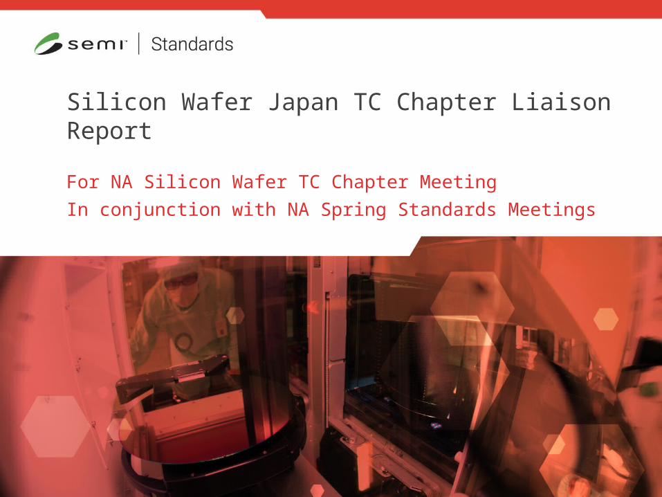
Leadership
• Committee Co-chairs– Naoyuki J. Kawai/ Independent– Tetsuya Nakai/ SUMCO
• Leadership Changes– None
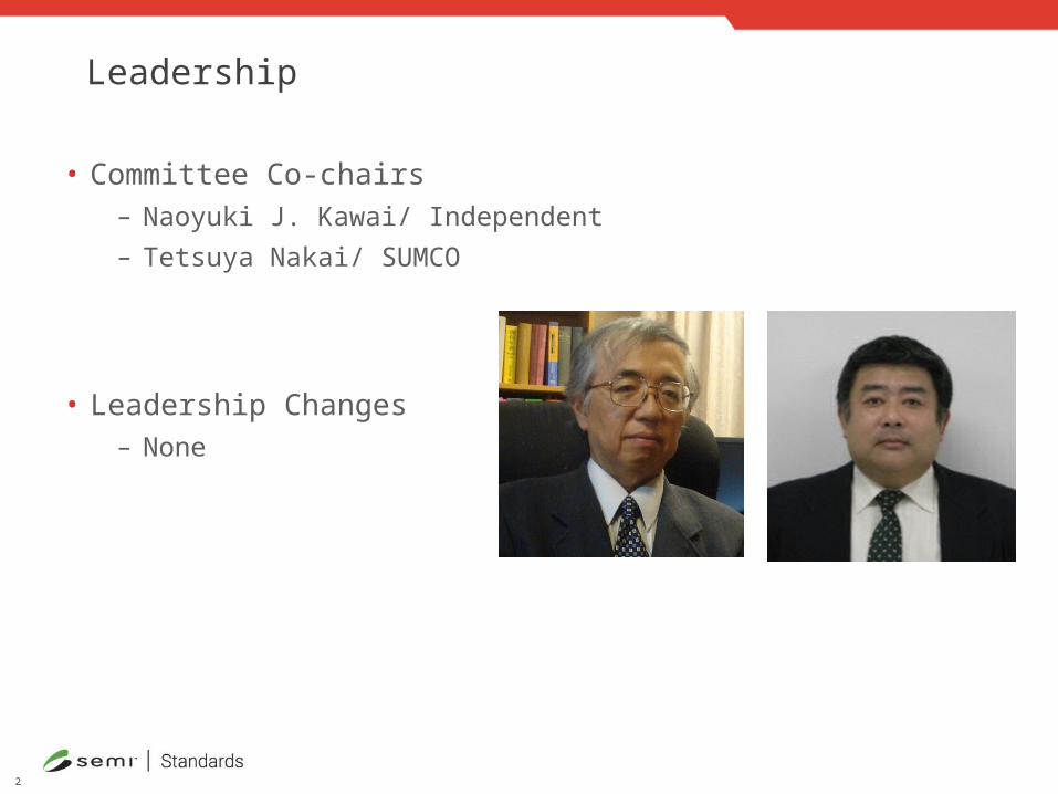
TC Chapter OrganizationJapan Silicon Wafer
Naoyuki Kawai (Independent)Tetsuya Nakai (SUMCO)
JWG TFSatoshi Akiyama (Raytex Optima)
Masanori Yoshise (Freelance)
Int’l SOI Wafers TFAtsushi Ogura (Meiji Univ)Tetsuya Nakai (SUMCO)
Int’l ASI TFMasami Ikota
(Hitachi High Technologies)
Int’l Annealed Wafers TFKoji Araki (Global Wafers Japan)
Int’l Polished Wafers TFYasuhiro Takamori
(Global Wafer Japan)
Int’l Epitaxial Wafers TFNaohisa Toda (Shinetsu Handotai)
Int’l Terminology TFTetsuya Nakai (SUMCO)
Int’l AWG TFSatoshi Akiyama (Raytex Optima)
JA Shipping Box TFShoji Komatsu (Acteon NEXT)Tsuyoshi Nagashima (Miraial)
Int’l 450mm Shipping Box TF
Shoji Komatsu (Acteon NEXT)
Fiducial Mark Interoperability TF
Tetsuya Nakai(SUMCO)
Int’l Test Method TFRyuji Takeda (GlobalWafers Japan)
Japan Test Method TFRyuji Takeda (GlobalWafers Japan)
Tsuyoshi Otsuki (Shin-Etsu Handotai)Mikako Omata (SCAS)
Surface Metal ChemicalAnalysis WG
Ryuji Takeda (Global Wafers Japan)Ryo Machida (SCAS)
BMD DZ WGSatoshi Akiyama (Raytex Optima)
Kazuo Moriya (Raytex Optima)
Bulk Heavy Metal Analysis
By Electrical Measurement WG
Masaru Akamatsu (KOBELCO)Shingo Sumie (KOBELCO)
GOI WGTsuyoshi Otsuki
(Sinetsu Handotai)
Surface Organic ContaminantAnalysis WG
Mikako Omata (SCAS)
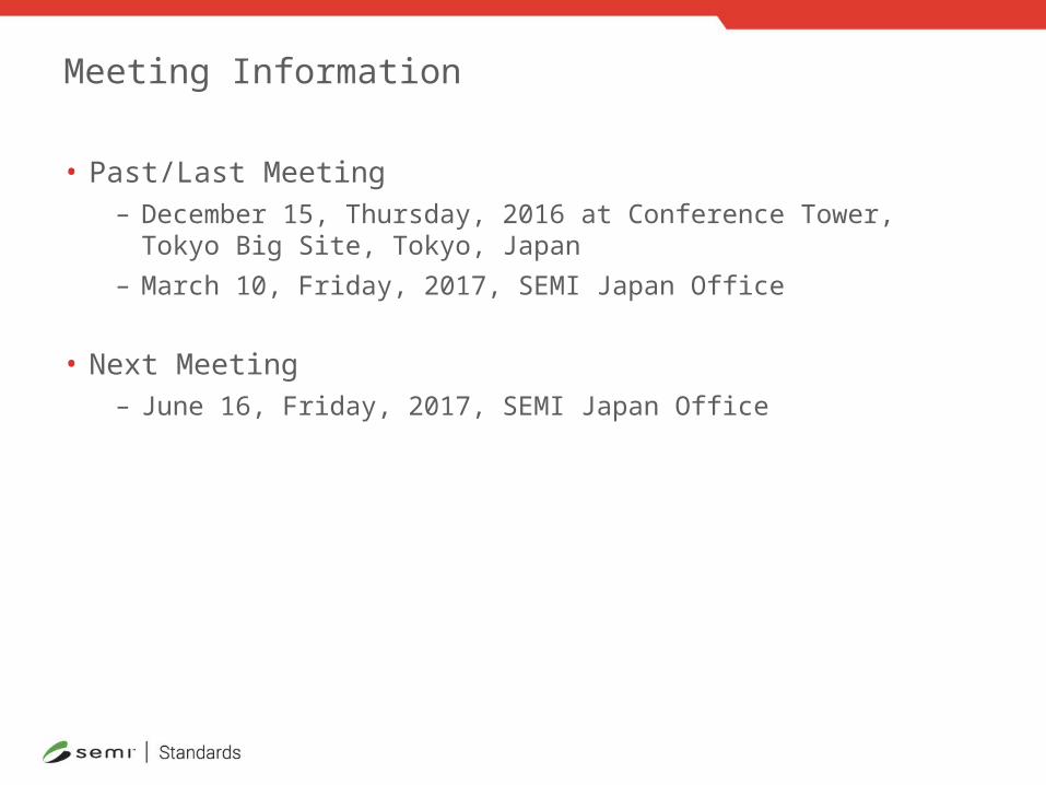
Meeting Information
• Past/Last Meeting– December 15, Thursday, 2016 at Conference Tower, Tokyo Big Site,
Tokyo, Japan– March 10, Friday, 2017, SEMI Japan Office
• Next Meeting– June 16, Friday, 2017, SEMI Japan Office
5
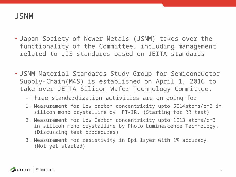
JSNM
• Japan Society of Newer Metals (JSNM) takes over the functionality of the Committee, including management related to JIS standards based on JEITA standards
• JSNM Material Standards Study Group for Semiconductor Supply-Chain(M4S) is established on April 1, 2016 to take over JETTA Silicon Wafer Technology Committee.
– Three standardization activities are on going for1. Measurement for Low carbon concentricity upto 5E14atoms/cm3 in silicon mono
crystalline by FT-IR. (Starting for RR test)2. Measurement for Low Carbon concentricity upto 1E13 atoms/cm3 in silicon
mono crystalline by Photo Luminescence Technology.(Discussing test procedures)
3. Measurement for resistivity in Epi layer with 1% accuracy. (Not yet started)
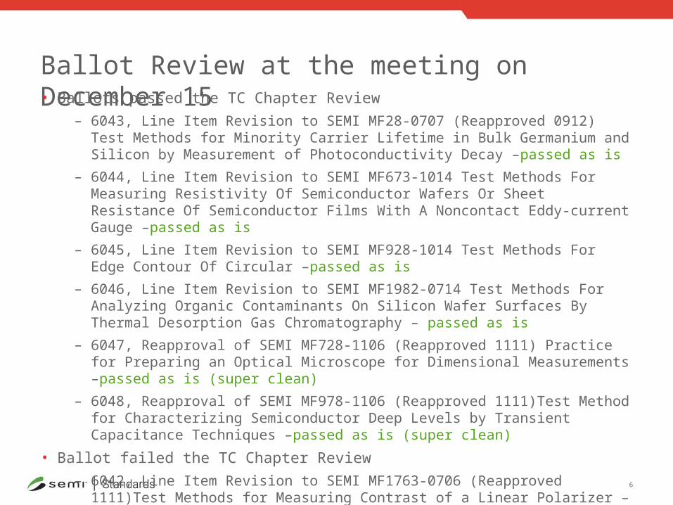
Ballot Review at the meeting on December 15• Ballots passed the TC Chapter Review
– 6043, Line Item Revision to SEMI MF28-0707 (Reapproved 0912) Test Methods for Minority Carrier Lifetime in Bulk Germanium and Silicon by Measurement of Photoconductivity Decay –passed as is
– 6044, Line Item Revision to SEMI MF673-1014 Test Methods For Measuring Resistivity Of Semiconductor Wafers Or Sheet Resistance Of Semiconductor Films With A Noncontact Eddy-current Gauge –passed as is
– 6045, Line Item Revision to SEMI MF928-1014 Test Methods For Edge Contour Of Circular –passed as is
– 6046, Line Item Revision to SEMI MF1982-0714 Test Methods For Analyzing Organic Contaminants On Silicon Wafer Surfaces By Thermal Desorption Gas Chromatography – passed as is
– 6047, Reapproval of SEMI MF728-1106 (Reapproved 1111) Practice for Preparing an Optical Microscope for Dimensional Measurements –passed as is (super clean)
– 6048, Reapproval of SEMI MF978-1106 (Reapproved 1111)Test Method for Characterizing Semiconductor Deep Levels by Transient Capacitance Techniques –passed as is (super clean)
• Ballot failed the TC Chapter Review– 6042, Line Item Revision to SEMI MF1763-0706 (Reapproved 1111)Test Methods for
Measuring Contrast of a Linear Polarizer – failed6
7
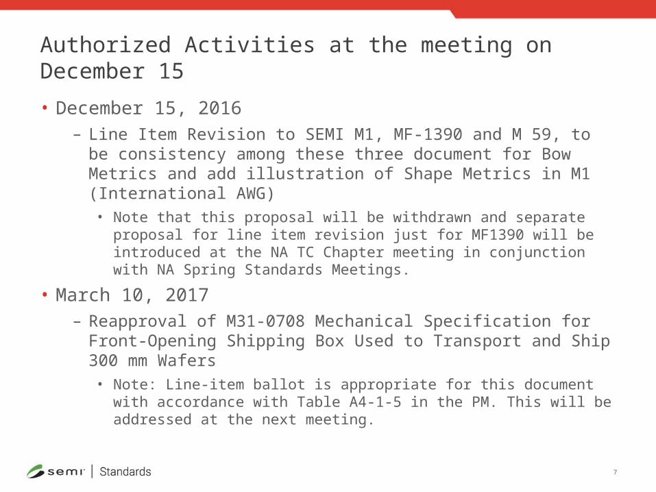
Authorized Activities at the meeting on December 15
• December 15, 2016– Line Item Revision to SEMI M1, MF-1390 and M 59, to be consistency
among these three document for Bow Metrics and add illustration of Shape Metrics in M1 (International AWG)• Note that this proposal will be withdrawn and separate proposal for line item
revision just for MF1390 will be introduced at the NA TC Chapter meeting in conjunction with NA Spring Standards Meetings.
• March 10, 2017– Reapproval of M31-0708 Mechanical Specification for Front-Opening
Shipping Box Used to Transport and Ship 300 mm Wafers• Note: Line-item ballot is appropriate for this document with accordance with
Table A4-1-5 in the PM. This will be addressed at the next meeting.
8
Five-year Review
• Reapproval of M31-0708 Mechanical Specification for Front-Opening Shipping Box Used to Transport and Ship 300 mm Wafers
– Note: Line-item ballot is appropriate for this document with accordance with Table A4-1-5 in the PM. This will be addressed at the next meeting.
9
SNARF Project Period Review
• Extended a project period– 5737: Revision of SEMI MF1391-1107, Test Method for Substitutional
Atomic Carbon Content of Silicon by Infrared Absorption
• The following documents will be reviewed at the next TC Chapter meeting
– 5769: New Standard: Test Method for Nitrogen Content in Silicon by Infrared Absorption
– 5770: Test Method for Bulk Micro Defect Density and Denuded Zone Width in Annealed Silicon Wafers
– 5772: Revision of MF391-0310: Test Methods for Minority Carrier Diffusion Length in Extrinsic Semiconductors by Measurement of Steady-state Surface photovoltage
– 5774: Sample Preparation Method for Minority Carrier Diffusion Length Measurement in Silicon Wafers by Surface Photovoltage Method
TF/ WG/ SG Reports -1
• International 450mm Shipping Box Task Force / JA Shipping Box Task Force – The TF decided not to address on standardization for re-use 300mm shipping.
• International Advanced Wafer Geometry Task Force / Japan AWG Task Force– Activity to be consistency of Bow Metrics between M1 and MF1390.
• International Test Method Task Force / Japan Test Method Task Force– Doc.5737B :Revision of SEMI MF1391-1107 (Reapproved 0912), Test Method
for Substitutional Atomic Carbon Content of Silicon by Infrared Absorption will be submitted to earlier ballot cycle in 2017
• International Advanced Surface Inspection Task Force– Drafting Doc. 6096: Line Item Revision to SEMI M53-0216 Practice for
Calibrating Scanning Surface Inspection Systems Using Certified Depositions of Monodispere Reference Spheres on Unpatterned Semiconductor Wafer Surfaces (Addition of a related information section to SEMI M53 regarding the relationship of calibrated sizes assigned to defects by surface inspection systems to their actual physical size )
11
TF/ WG/ SG Reports -2
• International Terminology Task Force– No special report from the task force but Japan TC Chapter discussed how
to maintain terminology in future and candidate options are:• To maintain as Aux document, this idea was withdrawn• To keep M59 with inactive status and new terminology will be defined in each
document• To continue to reapprove and issue the revision ballot when needed
– In any cases, there are some issues to be discussed and Silicon Water Global Technical Committee needs to get some consultation from Regulations Subcommittee.
– Following the discussion during NA Spring Standards Meetings, the Japan TC Chapter will develop the proposal at the next meeting
– Formal discussion will be held at GCS in SEMICON WEST
TF/ WG/ SG Reports -2
• International SOI Wafers Task Force– No special report
• International Polished Wafers Task Force– No special report
• International Epitaxial Wafers Task Force– No special report
• International Annealed Wafers Task Force– No special report
• Fiducial Mark Interoperability Task Force– This task force is under process of disbandment.– Japan Silicon Wafer TC Chapter agreed to disband this task force with
all agreement of other Technical Committees in Japan chapter, PI&C, I&C, Packaging and Traceability.
13
Other topics
• Proposal of New Standards, Specification for Lamella Carriers Used in Transmission Electron Microscopes
– According to the decision at the EU TC Chapter meeting in October during SEMICON Europa 2016, the meeting to introduce proposal was held on December 13 at SEMI Japan Office in conjunction with SEMICON Japan 2016• Back ground of this standardization• Presentation on “Enabling HVM TEM metrology support - standards for TEM
lamella carriers”• Proposed drafts of SNARF and TFOF
– Conducting Survey has been decided at the Japan PI&C TC Chapter Meeting• Currently contents of survey form is under drafting.
![ECTC 2008 리뷰 전자부품및패키징컨퍼런스 2008 리뷰_ 전자... · 2012-06-14 · 다. TSV(through silicon via)[1], WLP(wafer level packaging) 등과같은실리콘기반으로의패키징기술들도](https://img.pdfslide.tips/doc/110x75/5ee125a9ad6a402d666c21c0/ectc-2008-ee-eeoee-2008-ee-2012-06-14.jpg)