Embed Size (px)
Citation preview

7/25/2019 PQA50-T
http://slidepdf.com/reader/full/pqa50-t 1/7
cui.com
date 07/15/201
page 1 of 7
SERIES: PQA50-T DESCRIPTION: DC-DC CONVERTER
date
page 1 of 7
FEATURES
• up to 50 W isolated output
• 2:1 input range (18~36 Vdc, 36~75 Vdc)
• smaller package
• single, regulated output
• 1,500 Vdc isolation
• short circuit, over current, input under voltage protection
• inverse polarity protection
• remote on/off
• operating temperature range (-40~85°C)
• six sided metal shielding
• efficiency up to 91%
MODEL inputvoltage
outputvoltage
outputcurrent
outputpower
rippleand noise1
efciency
typ(Vdc)
range(Vdc) (Vdc)
min(mA)
max(A)
max(W)
max(mVp-p)
typ(%)
PQA50-D24-S3-T 24 18~36 3.3 500 10 33 150 89
PQA50-D24-S5-T 24 18~36 5 500 10 50 150 91
PQA50-D24-S12-T 24 18~36 12 208 4.167 50 150 91
PQA50-D24-S15-T 24 18~36 15 167 3.333 50 150 91
PQA50-D24-S24-T 24 18~36 24 104 2.083 50 150 91
PQA50-D48-S3-T 48 36~75 3.3 500 10 33 150 89
PQA50-D48-S5-T 48 36~75 5 500 10 50 150 91
PQA50-D48-S12-T 48 36~75 12 208 4.167 50 150 91PQA50-D48-S15-T 48 36~75 15 167 3.333 50 150 91
PQA50-D48-S24-T 48 36~75 24 104 2.083 50 150 91
Notes: 1. Ripple and noise are measured at 20 MHz BW by "parallel cable" method with 1 μF ceramic and 10 μF electrolytic capacitors on the output.
PART NUMBER KEY
PQA50 - DXX - SXX - TX
Input Voltage
Output Voltage
Base Number
Mounting Type
Heatsink"blank" = no heatsinkH = with heatsink
T = Chassis Mount
For more information, please visit the product page.

7/25/2019 PQA50-T
http://slidepdf.com/reader/full/pqa50-t 2/7
cui.com
CUI Inc SERIES: PQA50-T DESCRIPTION: DC-DC CONVERTER date 07/15/2015 page 2 o
INPUTparameter conditions/description min typ max units
operating input voltage24 Vdc input models48 Vdc input models
1836
2448
3675
VdcVdc
start-up voltage
input under voltage protection
24 Vdc input models48 Vdc input models 1836 VdcVdc
input over voltage protection24 Vdc input models48 Vdc input models
3675
VdcVdc
under/over voltage shutdown
input under voltage protection24 Vdc input models48 Vdc input models
1632
VdcVdc
input over voltage protection24 Vdc input models48 Vdc input models
4081
VdcVdc
surge voltagefor maximum of 1 second24 Vdc input models48 Vdc input models
-0.7-0.7
50100
VdcVdc
start-up time nominal input, constant load 10 ms
CTRL1
models ON (CTRL open or connect TTL high level, 3~12 Vdc)
models OFF (CTRL connect GND or low level, 0~1.2 Vdc)
input current (models OFF) 6 mA
lter pi lter
Note 1. CTRL pin voltage is referenced to GND.
OUTPUTparameter conditions/description min typ max units
line regulation full load, input voltage from low to high ±0.2 ±0.5 %
load regulation 10% to 100% load ±0.5 ±1 %
voltage accuracy ±1 ±3 %adjustability ±10 %
switching frequency PWM mode 320 kHz
transient recovery time 25% load step change 300 500 μs
transient response deviation 25% load step change ±3 ±5 %
temperature coefcient 100% load ±0.02 %/°C
PROTECTIONSparameter conditions/description min typ max units
over voltage protection2
3.3 Vdc output models5 Vdc output models12 Vdc output models15 Vdc output models24 Vdc output models
3.96.2151830
VdcVdcVdcVdcVdc
over current protection 135 %
short circuit protection continuous, automatic recovery, hiccup
over temperature protection 110 °C
Note 2. Module needs to be re-started after over voltage protection.
For more information, please visit the product page.

7/25/2019 PQA50-T
http://slidepdf.com/reader/full/pqa50-t 3/7
cui.com
CUI Inc SERIES: PQA50-T DESCRIPTION: DC-DC CONVERTER date 07/15/2015 page 3 o
SAFETY AND COMPLIANCEparameter conditions/description min typ max units
isolation voltage input to output at 1 mA for 1 minute 1,500 Vdc
isolation resistance input to output at 500 Vdc 1,000 MΩ
isolation capacitance input to output at 100 kHz, 0.1 Vdc 2,000 pF
conducted emissions CISPR22/EN55022 class B (external circuit required, see gure 1)
radiated emissions CISPR22/EN55022 class B (external circuit required, see gure 1)
ESD IEC/EN61000-4-2 class B, contact ± 4kV
radiated immunity IEC/EN61000-4-3 class A, 10V/m
EFT/burst IEC/EN61000-4-4 class B, ± 2kV (external circuit required, see gure 1)
surge IEC/EN61000-4-5 class B, ± 2kV (external circuit required, see gure 1)
conducted immunity IEC/EN61000-4-6 class A, 3 Vr.m.s
voltage dips & interruptions IEC/EN61000-4-29 class B, 0%-70%
MTBF as per MIL-HDBK-217F @ 25°C 1,000,000 hours
RoHS 2011/65/EU
ENVIRONMENTALparameter conditions/description min typ max units
operating temperature see derating curve -40 85 °C
storage temperature -55 125 °C
storage humidity non-condensing 5 95 %
case temperature at full load, operating temperature curve range 105 °C
vibration 10~55 Hz, 30 min. along x, y, and z 10 G
MECHANICALparameter conditions/description min typ max units
dimensionschassis mount: 76.0 x 31.5 x 21.2chassis mount with heatsink: 76.0 x 31.5 x 25.1
mmmm
case material aluminum alloy
weightchassis mountchassis mount with heatsink
5765
gg
For more information, please visit the product page.

7/25/2019 PQA50-T
http://slidepdf.com/reader/full/pqa50-t 4/7
cui.com
CUI Inc SERIES: PQA50-T DESCRIPTION: DC-DC CONVERTER date 07/15/2015 page 4 o
PIN CONNECTIONS
PIN Function
1 CTRL
2 GND
3 Vin
4 Trim
5 0V
6 +Vo
units: mm[inch]tolerance: ±0.50[±0.020]
wire range: 24~12 AWG
Top View
Front View
CHASSIS MOUNT WITH HEATSINK
PIN CONNECTIONS
PIN Function
1 CTRL
2 GND
3 Vin
4 Trim
5 0V
6 +Vo
units: mm[inch]tolerance: ±0.50[±0.020]
wire range: 24~12 AWG
Top View
Front View
CHASSIS MOUNT
MECHANICAL DRAWING
For more information, please visit the product page.

7/25/2019 PQA50-T
http://slidepdf.com/reader/full/pqa50-t 5/7
cui.com
CUI Inc SERIES: PQA50-T DESCRIPTION: DC-DC CONVERTER date 07/15/2015 page 5 o
Output Voltage ≤ 5Vdc
Recommended external circuit components
Vin (Vdc) 24 48
C0 330μF/50V 330μF/100V
CY1, CY2 1nF/2kV 1nF/2kV
LCM 2.2mH 2.2mH
EMC RECOMMENDED CIRCUIT
DERATING CURVES
100
80
60
40
20
Ambient Temperature (°C)
L o a d ( % )
-40 -20 0 20 40 100
Safe operating area
55 65 85
Without heatsink
With heatsink
100
80
60
40
20
Ambient Temperature (°C)
L o a d ( % )
-40 -20 0 20 40 85 100
Safe operating area
60 70
Without heatsink
With heatsink
Output Voltage > 5Vdc
Figure 1 Table 1
Vin
GND
+Vo
0V
DC/DC LOAD
LCM
C0
CY
Vin
GND
CY 1
2
Cout
TEST CONFIGURATION
DCCin
Lin
DC Load
Oscilloscope
CurrentProbe
Note: 1. Input reected-ripple current is measured with an inductor Lin and Capacitor Cin to simulate source impedance.
External components
Lin 4.7μH
Cin 220μF, ESR < 1.0Ω
at 100 kHz
Figure 2 Table 2
Note: 1. See Table 3 for Cout values.
For more information, please visit the product page.
7/25/2019 PQA50-T
http://slidepdf.com/reader/full/pqa50-t 6/7
cui.com
CUI Inc SERIES: PQA50-T DESCRIPTION: DC-DC CONVERTER date 07/15/2015 page 6 o
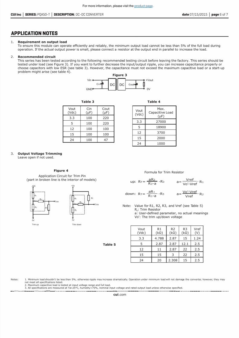
1. Requirement on output load To ensure this module can operate efciently and reliably, the minimum output load cannot be less than 5% of the full load duringoperation. If the actual output power is small, please connect a resistor at the output end in parallel to increase the load.
2. Recommended circuit
This series has been tested according to the following recommended testing circuit before leaving the factory. This series should betested under load (see Figure 3). If you want to further decrease the input/output ripple, you can increase capacitance properly orchoose capacitors with low ESR (see table 3). However, the capacitance must not exceed the maximum capacitive load or a start-upproblem might arise (see table 4).
3. Output Voltage Trimming Leave open if not used.
Formula for Trim Resistor
Application Circuit for Trim Pin(part in broken line is the interior of models)
Note: Value for R1, R2, R3, and Vref (see Table 5)R
T: Trim Resistor
a: User-dened parameter, no actual meanings Vo': The trim up/down voltage
up: a= Vref
Vo’-Vref R 1R =
aR 2
R -a2-R 3
down: a=Vref
Vo’-Vref R 2R =T
T
aR 1
R -a1-R 3
APPLICATION NOTES
Figure 3
Table 3 Table 4
Table 5
Figure 4
Vout(Vdc)
Cin(µF)
Cout(µF)
3.3 100 2205 100 220
12 100 100
15 100 100
24 100 47
Notes: 1. Minimum load shouldn't be less than 5%, otherwise ripple may increase dramatically. Operation under minimum load will not damage the converter, however, they manot meet all specications listed.
2. Maximum capacitive load is tested at input voltage range and full load. 3. All specications are measured at Ta=25°C, humidity<75%, nominal input voltage and rated output load unless otherwise specied.
+Vo
0V
R2
R1
R3
Vref
RT
Trim
0V
R2
R1
R3
V ref
RT
Trim
+Vo
Trim up Trim down
DC DC
Vin
GND
+Vout
0V
Ci n
Vout(Vdc)
Max.Capacitive Load
(μF)
3.3 27000
5 18900
12 3700
15 2000
24 1000
Vout(Vdc)
R1(kΩ)
R2(kΩ)
R3(kΩ)
Vref (V)
3.3 4.788 2.87 15 1.24
5 2.87 2.87 12.1 2.5
12 11 2.87 22 2.5
15 15 3 22 2.5
24 20 2.308 15 2.5
For more information, please visit the product page.

7/25/2019 PQA50-T
http://slidepdf.com/reader/full/pqa50-t 7/7
CUI Inc SERIES: PQA50-T DESCRIPTION: DC-DC CONVERTER date 07/15/2015 page 7 o
CUI offers a two (2) year limited warranty. Complete warranty information is listed on our website.
CUI reserves the right to make changes to the product at any time without notice. Information provided by CUI is believed to be accurate and reliable. However, no responsibility isassumed by CUI for its use, nor for any infringements of patents or other rights of third parties which may result from its use.
CUI products are not authorized or warranted for use as critical components in equipment that requires an extremely high level of reliability. A critical component is any component
life support device or system whose failure to perform can be reasonably expected to cause the failure of the life support device or system, or to affect its safety or effectiveness.
Headquarters20050 SW 112th Ave.Tualatin, OR 97062800.275.4899
rev. description date
1.0 initial release 01/21/2014
1.01 updated datasheet 07/15/2015The revision history provided is for informational purposes only and is believed to be accurate.
REVISION HISTORY
For more information, please visit the product page.


![3 4( ) 056! 870 9:! 2 ;! 9 :! ?, :3 @ !- A-BDC ... · y^` gh` wvwgex}y^kti \ xwi cek o\^fU` ^ kEi `s` y^\ gekofU`d t t t t t t t t t t t t t t t t t t ]e m \ r `&id\](https://img.pdfslide.tips/doc/110x75/6082bd294d58915606292210/3-4-056-870-9-2-9-3-a-bdc-y-gh-wvwgexykti-xwi-cek.jpg)