Embed Size (px)
Citation preview
Page 1 of 11
Document No. 70-0177-05 www.psemi.com ©2005-2008 Peregrine Semiconductor Corp. All rights reserved.
Parameter Conditions Typical Units
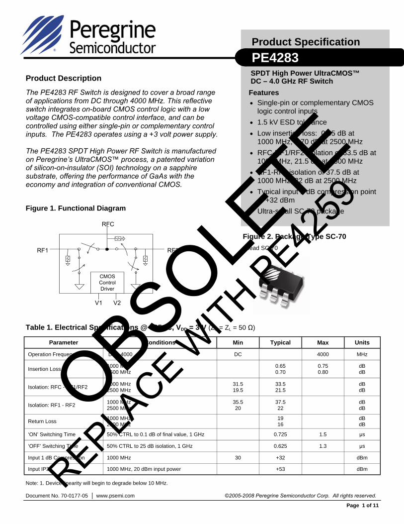
Operation Frequency1 DC - 4000 MHz
Insertion Loss 1000 MHz 2500 MHz
0.65 0.70
dB dB
Isolation: RFC - RF1/RF2 1000 MHz 2500 MHz
33.5 21.5
dB dB
Isolation: RF1 - RF2 1000 MHz 2500 MHz
37.5 22
dB dB
‘ON’ Switching Time 50% CTRL to 0.1 dB of final value, 1 GHz 0.725 µs
‘OFF’ Switching Time 50% CTRL to 25 dB isolation, 1 GHz 0.625 µs
Input 1 dB Compression 1000 MHz +32 dBm
Input IP3 1000 MHz, 20 dBm input power +53 dBm
Min
DC
31.5 19.5
35.5 20
30
Max
4000
0.75 0.80
1.5
1.3
Return Loss 1000 MHz 2500 MHz
19 16
dB dB
RFC
RF1 RF2
CMOSControlDriver
V1 V2
The PE4283 RF Switch is designed to cover a broad range of applications from DC through 4000 MHz. This reflective switch integrates on-board CMOS control logic with a low voltage CMOS-compatible control interface, and can be controlled using either single-pin or complementary control inputs. The PE4283 operates using a +3 volt power supply. The PE4283 SPDT High Power RF Switch is manufactured on Peregrine’s UltraCMOS™ process, a patented variation of silicon-on-insulator (SOI) technology on a sapphire substrate, offering the performance of GaAs with the economy and integration of conventional CMOS.
Product Specification
SPDT High Power UltraCMOS™ DC – 4.0 GHz RF Switch Product Description
Figure 1. Functional Diagram
PE4283
Features • Single-pin or complementary CMOS
logic control inputs
• 1.5 kV ESD tolerance
• Low insertion loss: 0.65 dB at 1000 MHz, 0.70 dB at 2500 MHz
• RFC-RF1/RF2 isolation of 33.5 dB at 1000 MHz, 21.5 dB at 2500 MHz
• RF1-RF2 isolation of 37.5 dB at 1000 MHz, 22 dB at 2500 MHz
• Typical input 1 dB compression point of +32 dBm
• Ultra-small SC-70 package
Note: 1. Device linearity will begin to degrade below 10 MHz.
Table 1. Electrical Specifications @ +25 °C, VDD = 3 V (ZS = ZL = 50 Ω )
Figure 2. Package Type SC-70 6-lead SC-70
OBSOLETE
REPLACE W
ITH PE42
59
Product Specification PE4283
Page 2 of 11
©2005-2008 Peregrine Semiconductor Corp. All rights reserved. Document No. 70-0177-05 UltraCMOS™ RFIC Solutions
Table 2. Pin Descriptions
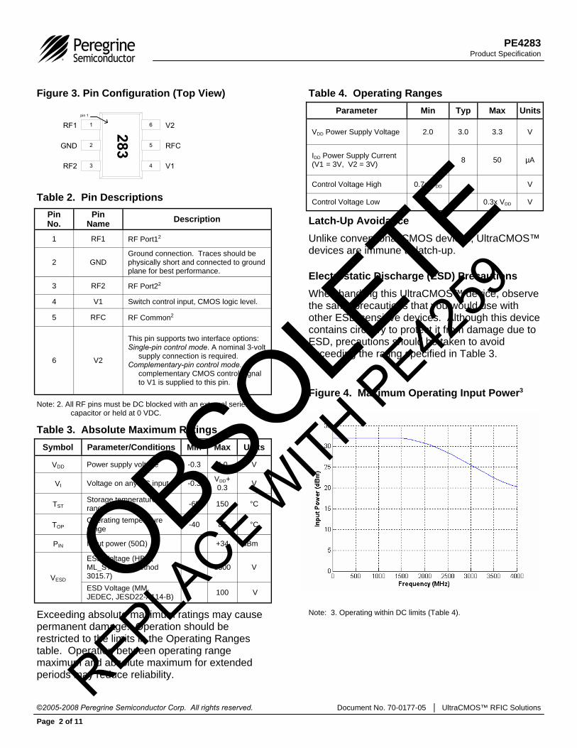
Electrostatic Discharge (ESD) Precautions
When handling this UltraCMOS™ device, observe the same precautions that you would use with other ESD-sensitive devices. Although this device contains circuitry to protect it from damage due to ESD, precautions should be taken to avoid exceeding the rating specified in Table 3.
Latch-Up Avoidance
Unlike conventional CMOS devices, UltraCMOS™ devices are immune to latch-up.
Table 4. Operating Ranges Figure 3. Pin Configuration (Top View)
1
2
3 4
5
6 V2
RFC
V1
RF1
GND
RF2
283
pin 1
Pin No.
Pin Name Description
1 RF1 RF Port12
2 GND Ground connection. Traces should be physically short and connected to ground plane for best performance.
3 RF2 RF Port22
4 V1 Switch control input, CMOS logic level.
5 RFC RF Common2
6 V2
This pin supports two interface options: Single-pin control mode. A nominal 3-volt
supply connection is required. Complementary-pin control mode. A
complementary CMOS control signal to V1 is supplied to this pin.
Parameter Min Typ Max Units
VDD Power Supply Voltage 2.0 3.0 3.3 V
IDD Power Supply Current (V1 = 3V, V2 = 3V)
8 50 µA
Control Voltage High 0.7x VDD V
Control Voltage Low 0.3x VDD V
Note: 2. All RF pins must be DC blocked with an external series capacitor or held at 0 VDC.
Table 3. Absolute Maximum Ratings
Symbol Parameter/Conditions Min Max Units
VDD Power supply voltage -0.3 4.0 V
VI Voltage on any DC input -0.3 VDD+ 0.3
V
TST Storage temperature range
-65 150 °C
TOP Operating temperature range
-40 85 °C
PIN Input power (50Ω) +34 dBm
VESD
ESD Voltage (HBM, ML_STD 883 Method 3015.7)
1500 V
ESD Voltage (MM, JEDEC, JESD22-A114-B)
100 V
Exceeding absolute maximum ratings may cause permanent damage. Operation should be restricted to the limits in the Operating Ranges table. Operation between operating range maximum and absolute maximum for extended periods may reduce reliability.
Figure 4. Maximum Operating Input Power3
Note: 3. Operating within DC limits (Table 4).
OBSOLETE
REPLACE W
ITH PE42
59

Product Specification PE4283
Page 3 of 11
©2005-2008 Peregrine Semiconductor Corp. All rights reserved. Document No. 70-0177-05 www.psemi.com
Control Voltages Signal Path
Pin 6 (V2) = VDD Pin 4 (V1) = High
RFC to RF1
Pin 6 (V2) = VDD Pin 4 (V1) = Low
RFC to RF2
Table 5. Single-pin Control Logic Truth Table
Table 6. Complementary-pin Control Logic Truth Table
Control Voltages Signal Path
Pin 6 (V2 ) = Low Pin 4 (V1) = High
RFC to RF1
Pin 6 (V2) = High Pin 4 (V1) = Low
RFC to RF2
Control Logic Input
The PE4283 is a versatile RF CMOS switch that supports two operating control modes; single-pin control mode and complementary-pin control mode. Single-pin control mode enables the switch to operate with a single control pin (pin 4) supporting a +3-volt CMOS logic input, and requires a dedicated +3-volt power supply connection (pin 6). This mode of operation reduces the number of control lines required and simplifies the switch control interface typically derived from a CMOS µProcessor I/O port. Complementary-pin control mode allows the switch to operate using complementary control pins V1 and V2 (pins 4 & 6), that can be directly driven by +3-volt CMOS logic or a suitable µProcessor I/O port. This enables the PE4283 to operate in positive control voltage mode within the PE4283 operating limits.
OBSOLETE
REPLACE W
ITH PE42
59
Product Specification PE4283
Page 4 of 11
©2005-2008 Peregrine Semiconductor Corp. All rights reserved. Document No. 70-0177-05 UltraCMOS™ RFIC Solutions
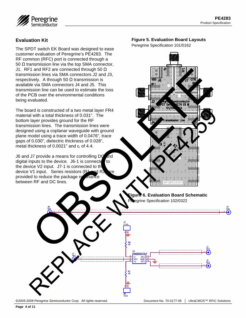
Evaluation Kit
The SPDT switch EK Board was designed to ease customer evaluation of Peregrine’s PE4283. The RF common (RFC) port is connected through a 50 Ω transmission line via the top SMA connector, J1. RF1 and RF2 are connected through 50 Ω transmission lines via SMA connectors J2 and J3, respectively. A through 50 Ω transmission is available via SMA connectors J4 and J5. This transmission line can be used to estimate the loss of the PCB over the environmental conditions being evaluated. The board is constructed of a two metal layer FR4 material with a total thickness of 0.031”. The bottom layer provides ground for the RF transmission lines. The transmission lines were designed using a coplanar waveguide with ground plane model using a trace width of 0.0476”, trace gaps of 0.030”, dielectric thickness of 0.028”, metal thickness of 0.0021” and εr of 4.4. J6 and J7 provide a means for controlling DC and digital inputs to the device. J6-1 is connected to the device V2 input. J7-1 is connected to the device V1 input. Series resistors (R1 and R2) are provided to reduce the package resonance between RF and DC lines.
Figure 5. Evaluation Board Layouts
Figure 6. Evaluation Board Schematic Peregrine Specification 102/0322
Peregrine Specification 101/0162
OBSOLETE
REPLACE W
ITH PE42
59
Product Specification PE4283
Page 5 of 11
©2005-2008 Peregrine Semiconductor Corp. All rights reserved. Document No. 70-0177-05 www.psemi.com
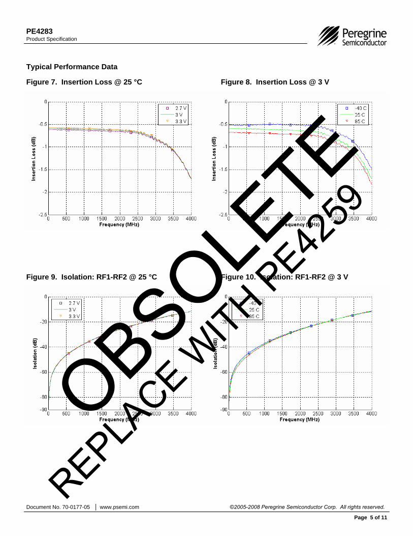
Figure 8. Insertion Loss @ 3 V Figure 7. Insertion Loss @ 25 °C
Typical Performance Data
Figure 9. Isolation: RF1-RF2 @ 25 °C Figure 10. Isolation: RF1-RF2 @ 3 V
OBSOLETE
REPLACE W
ITH PE42
59
Product Specification PE4283
Page 6 of 11
©2005-2008 Peregrine Semiconductor Corp. All rights reserved. Document No. 70-0177-05 UltraCMOS™ RFIC Solutions
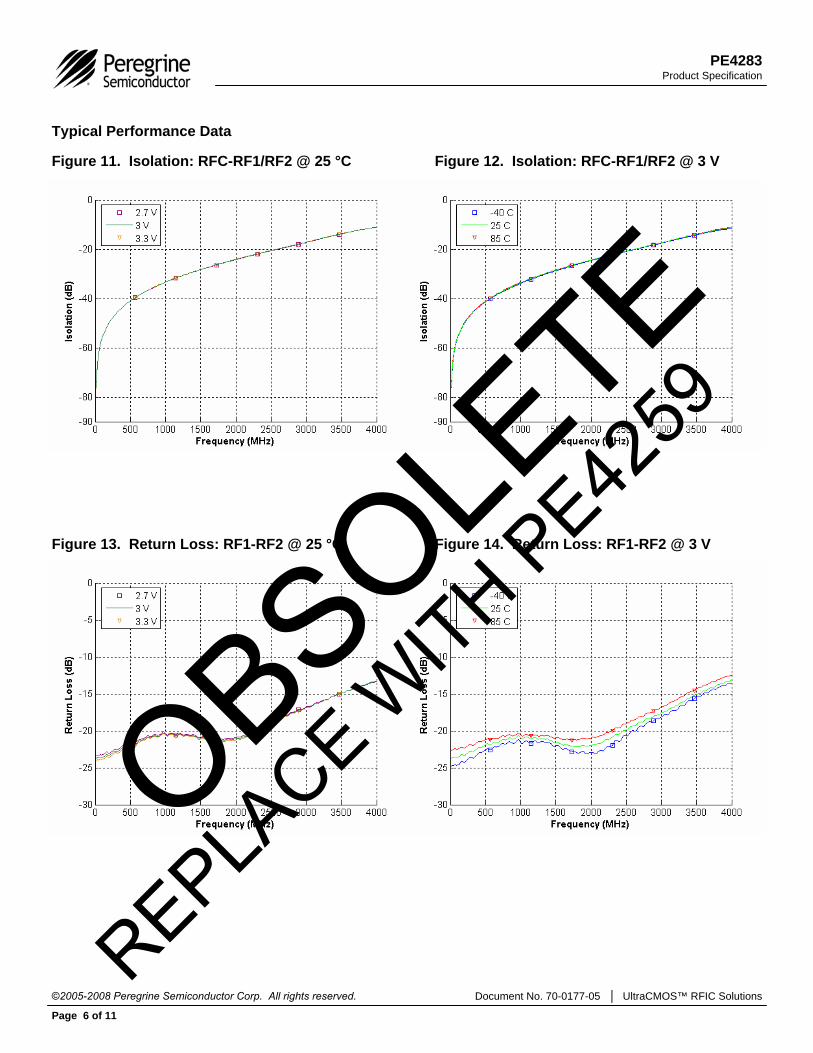
Figure 13. Return Loss: RF1-RF2 @ 25 °C Figure 14. Return Loss: RF1-RF2 @ 3 V
Typical Performance Data
Figure 11. Isolation: RFC-RF1/RF2 @ 25 °C Figure 12. Isolation: RFC-RF1/RF2 @ 3 V
OBSOLETE
REPLACE W
ITH PE42
59
Product Specification PE4283
Page 7 of 11
©2005-2008 Peregrine Semiconductor Corp. All rights reserved. Document No. 70-0177-05 www.psemi.com
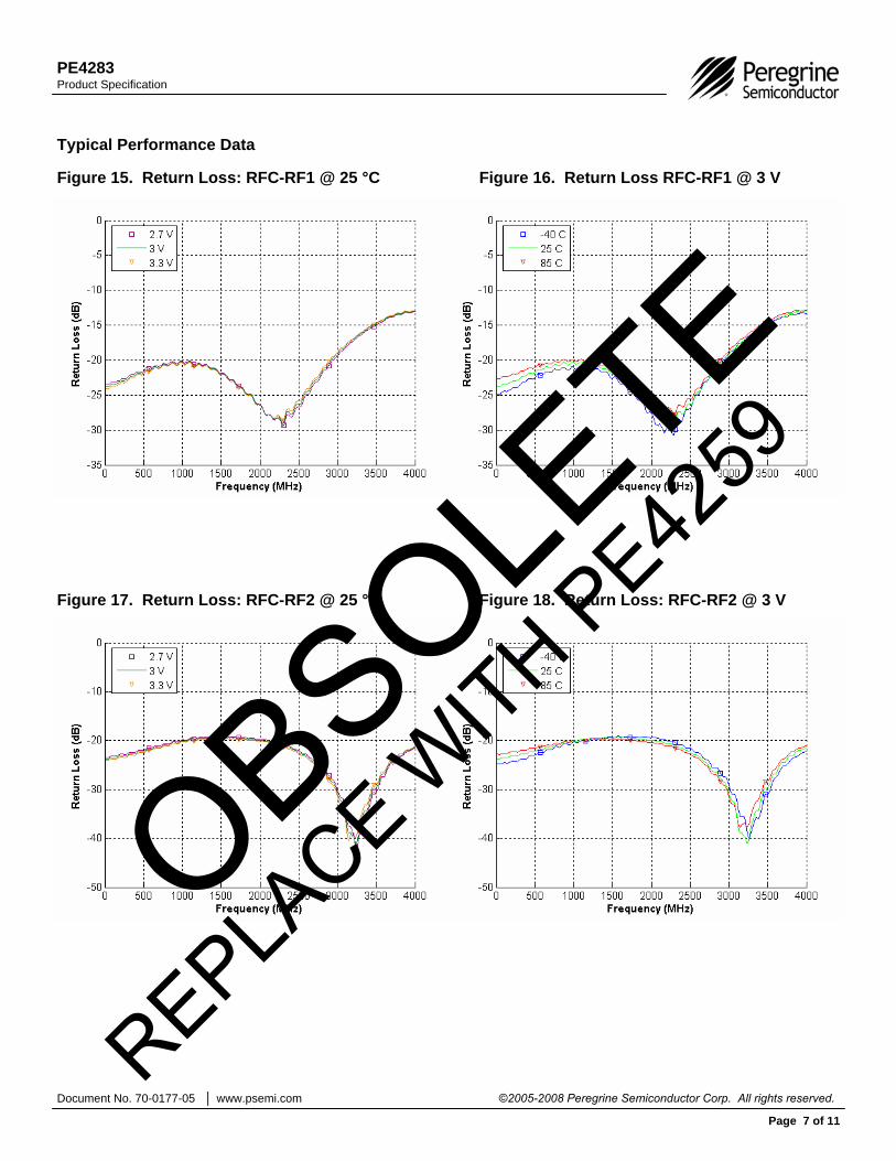
Typical Performance Data
Figure 15. Return Loss: RFC-RF1 @ 25 °C Figure 16. Return Loss RFC-RF1 @ 3 V
Figure 17. Return Loss: RFC-RF2 @ 25 °C Figure 18. Return Loss: RFC-RF2 @ 3 V
OBSOLETE
REPLACE W
ITH PE42
59
Product Specification PE4283
Page 8 of 11
©2005-2008 Peregrine Semiconductor Corp. All rights reserved. Document No. 70-0177-05 UltraCMOS™ RFIC Solutions
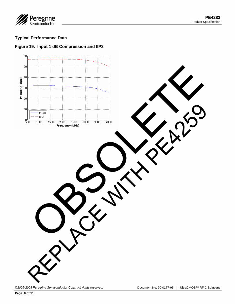
Figure 19. Input 1 dB Compression and IIP3
Typical Performance Data
OBSOLETE
REPLACE W
ITH PE42
59
Product Specification PE4283
Page 9 of 11
©2005-2008 Peregrine Semiconductor Corp. All rights reserved. Document No. 70-0177-05 www.psemi.com
1.802.20
0.65BSC
1.802.40
1.151.35
0.150.30
0.801.10
0.801.00
0.100.30
0.100.40
0.100.18
0.000.10
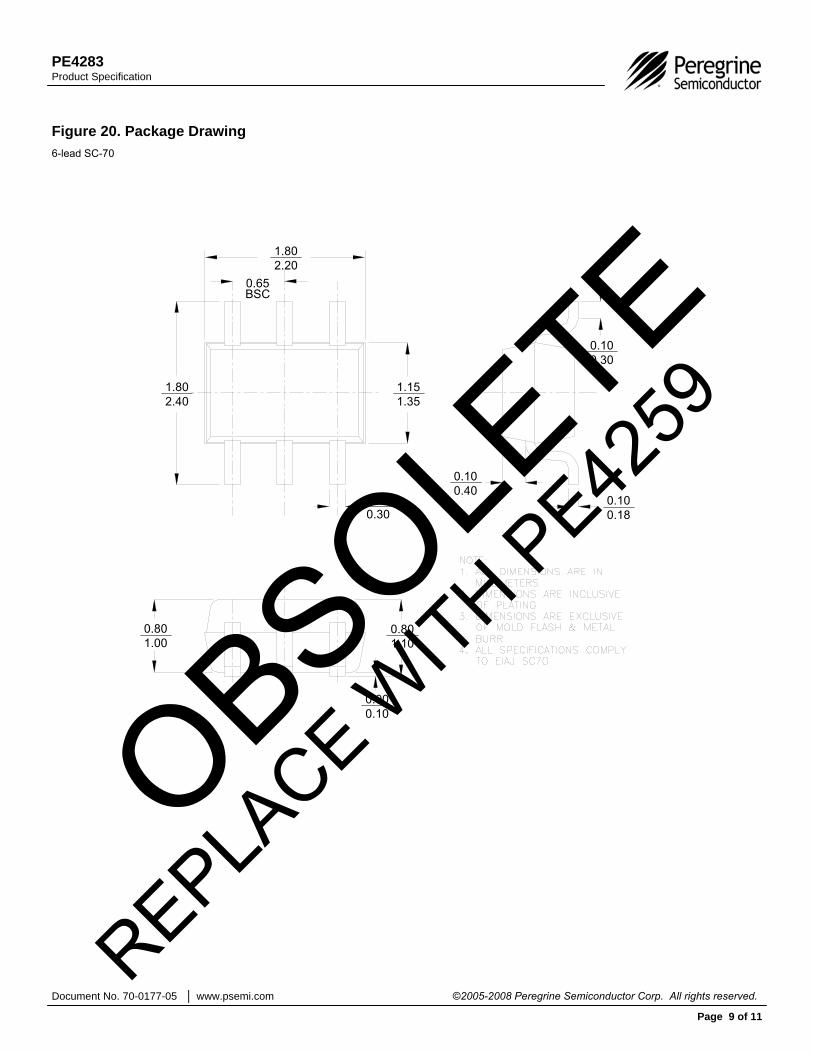
Figure 20. Package Drawing 6-lead SC-70
OBSOLETE
REPLACE W
ITH PE42
59

Product Specification PE4283
Page 10 of 11
©2005-2008 Peregrine Semiconductor Corp. All rights reserved. Document No. 70-0177-05 UltraCMOS™ RFIC Solutions
Table 7. Ordering Information
Order Code Part Marking Description Package Shipping Method
4283-00 PE4283-EK PE4283-06SC70-EK Evaluation Kit 1 / Box
4283-51 283 PE4283G-06SC70-7680A Green 6-lead SC-70 7680 units / Canister
4283-52 283 PE4283G-06SC70-3000C Green 6-lead SC-70 3000 units / T&R
Figure 21. Tape and Reel Specifications
Pin 1
Tape Feed Direction
OBSOLETE
REPLACE W
ITH PE42
59
Product Specification PE4283
Page 11 of 11
©2005-2008 Peregrine Semiconductor Corp. All rights reserved. Document No. 70-0177-05 www.psemi.com
Sales Offices
The Americas
Peregrine Semiconductor Corporation 9380 Carroll Park Drive San Diego, CA 92121 Tel: 858-731-9400 Fax: 858-731-9499
Europe Peregrine Semiconductor Europe
Bâtiment Maine 13-15 rue des Quatre Vents F-92380 Garches, France Tel: +33-1-4741-9173 Fax : +33-1-4741-9173
For a list of representatives in your area, please refer to our Web site at: www.psemi.com
Data Sheet Identification
Advance Information
The product is in a formative or design stage. The data sheet contains design target specifications for product development. Specifications and features may change in any manner without notice. Preliminary Specification
The data sheet contains preliminary data. Additional data may be added at a later date. Peregrine reserves the right to change specifications at any time without notice in order to supply the best possible product.
Product Specification
The data sheet contains final data. In the event Peregrine decides to change the specifications, Peregrine will notify customers of the intended changes by issuing a DCN (Document Change Notice).
The information in this data sheet is believed to be reliable. However, Peregrine assumes no liability for the use of this information. Use shall be entirely at the user’s own risk. No patent rights or licenses to any circuits described in this data sheet are implied or granted to any third party. Peregrine’s products are not designed or intended for use in devices or systems intended for surgical implant, or in other applications intended to support or sustain life, or in any application in which the failure of the Peregrine product could create a situation in which personal injury or death might occur. Peregrine assumes no liability for damages, including consequential or incidental damages, arising out of the use of its products in such applications. The Peregrine name, logo, and UTSi are registered trademarks and UltraCMOS, HaRP and MultiSwitch are trademarks of Peregrine Semiconductor Corp.
Space and Defense Products Americas:
Tel: 858-731-9453 Europe, Asia Pacific: 180 Rue Jean de Guiramand 13852 Aix-En-Provence Cedex 3, France Tel: +33-4-4239-3361 Fax: +33-4-4239-7227
Peregrine Semiconductor, Asia Pacific (APAC) Shanghai, 200040, P.R. China Tel: +86-21-5836-8276 Fax: +86-21-5836-7652 Peregrine Semiconductor, Korea #B-2607, Kolon Tripolis, 210 Geumgok-dong, Bundang-gu, Seongnam-si Gyeonggi-do, 463-943 South Korea Tel: +82-31-728-3939 Fax: +82-31-728-3940 Peregrine Semiconductor K.K., Japan Teikoku Hotel Tower 10B-6 1-1-1 Uchisaiwai-cho, Chiyoda-ku Tokyo 100-0011 Japan Tel: +81-3-3502-5211 Fax: +81-3-3502-5213
OBSOLETE
REPLACE W
ITH PE42
59


![Complementary Material · 2018. 5. 25. · Page 3C.1 Chapter 3. Complementary Material Chapter 3 Complementary Material Lemma 3C.1 [1] If a signal φ:[0, )∞→Rn is PE and satisfies](https://img.pdfslide.tips/doc/110x75/61249971045df63b1d59b32b/complementary-material-2018-5-25-page-3c1-chapter-3-complementary-material.jpg)