Embed Size (px)
Citation preview
CU13
PROYECTO CU13
DISEÑO EN VHDL DE UN CONTADOR UNIVERSAL INDEPENDIENTE PROGRAMABLE DE 4 DÍGITOS BCD. PERMITE TRES MODOS DIFERENTES DE MEDICIÓN: --FRECUENCIA. --PERÍODO. --INTERVALO DE TIEMPO.
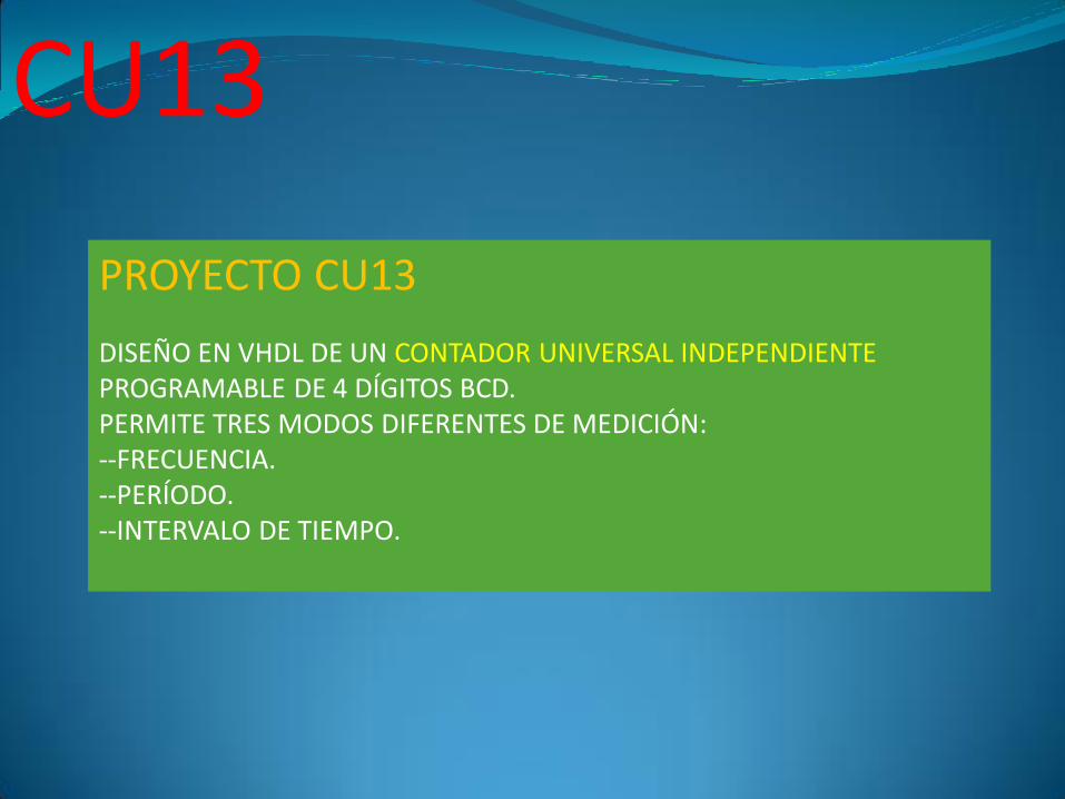
Contador Universal
Canal A
Clock_50MHz
Reset
Out_bcd3 Out_bcd2 Out_bcd1 Out_bcd0
Overflow End of Conversion
Mode
Canal B
Medidor de Frecuencias Medidor de Período Medidor de Intervalo de Tiempo
Sergio Noriega - 2015
Contador Universal
Modos de funcionamiento
Salida de 4 dígitos BCD. Indicaciones de «overflow» y «fin de conversión». Base de tiempo programable. Adquisición «one shot» ó «free-running».
CU13
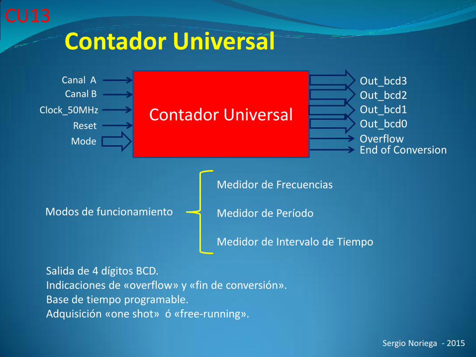
Medidor de Frecuencia
Canal A
Out_ovf Out_eoc
Mode
Canal B
Contador BCD x4
Out_bcd3 Out_bcd2 Out_bcd1 Out_bcd0
Out_ovf
Out_bcd3 Out_bcd2 Out_bcd1 Out_bcd0
Canal A
Reloj 50MHz
Reset
Base de Tiempo
ena0
reloj
Reloj 50MHz
Mode
Reset
Sergio Noriega - 2015
"xxxxxxxxxxx00xx"
bt
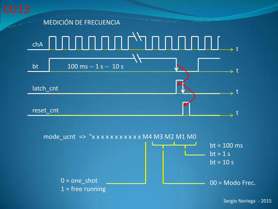
MEDICIÓN DE FRECUENCIA
CU13
Sergio Noriega - 2015
bt
latch_cnt
reset_cnt
t
t
t
t
chA
100 ms -- 1 s -- 10 s
mode_ucnt => "x x x x x x x x x x x M4 M3 M2 M1 M0
0 = one_shot 1 = free running
bt = 100 ms bt = 1 s bt = 10 s
00 = Modo Frec.
MEDICIÓN DE FRECUENCIA
CU13
Sergio Noriega - 2015
S0/0 S1/0
S3/0 S2/1
bt=0
bt=1
bt=0
bt=1
bt=0
bt=0 bt=1
bt=1
St0/0 St1/0
St3/0 St2/1
latch_cnt=0
1
0
1
0
0 1
1
latch_cnt rst_cnt
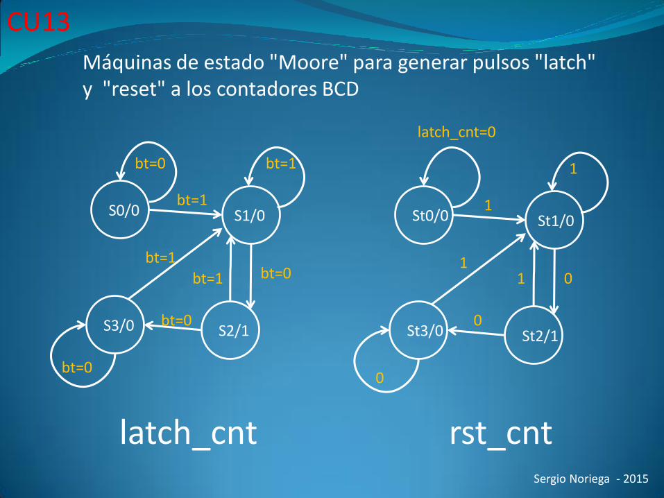
Máquinas de estado "Moore" para generar pulsos "latch" y "reset" a los contadores BCD
CU13
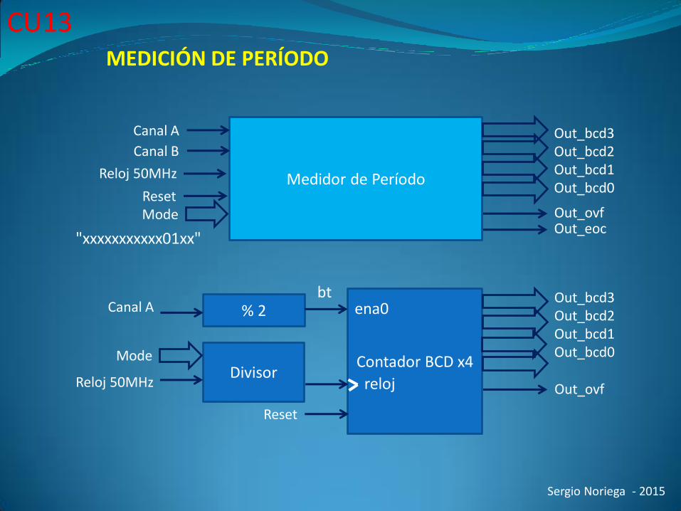
Medidor de Período
Canal A
Out_ovf Out_eoc
Mode
Canal B
Contador BCD x4
Out_bcd3 Out_bcd2 Out_bcd1 Out_bcd0
Out_ovf
Out_bcd3 Out_bcd2 Out_bcd1 Out_bcd0
Canal A
Reloj 50MHz
Reset
% 2 ena0
reloj Reloj 50MHz
Reset
Sergio Noriega - 2015
"xxxxxxxxxxx01xx"
bt
Divisor Mode
MEDICIÓN DE PERÍODO
CU13

Sergio Noriega - 2015
bt
latch_cnt
reset_cnt
t
t
t
t
10MHZ/1MHZ/ 100KHZ/10KHZ
mode_ucnt => "x x x x x x x x x x x M4 M3 M2 M1 M0
0 = one_shot 1 = free running
01 = Modo Período
MEDICIÓN DE PERÍODO
Período de chA Período de chA
00 = clk => 10 MHz 01 = clk => 1 MHz 10 = clk => 100 KHz 11 = clk => 10 KHz
CU13
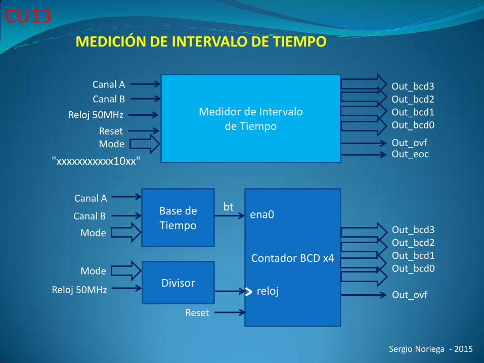
Medidor de Intervalo de Tiempo
Canal A
Out_ovf Out_eoc
Mode
Canal B
Contador BCD x4
Out_bcd3 Out_bcd2 Out_bcd1 Out_bcd0
Out_ovf
Out_bcd3 Out_bcd2 Out_bcd1 Out_bcd0
Canal A
Reloj 50MHz
Reset
Base de Tiempo
ena0
reloj Reloj 50MHz
Reset
Sergio Noriega - 2015
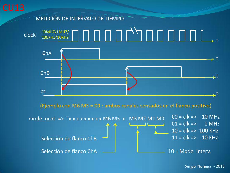
"xxxxxxxxxxx10xx"
bt
Divisor Mode
Canal B
Mode
MEDICIÓN DE INTERVALO DE TIEMPO
CU13
Sergio Noriega - 2015
bt
ChB
t
t
t
t
10MHZ/1MHZ/ 100KHZ/10KHZ
mode_ucnt => "x x x x x x x x x M6 M5 x M3 M2 M1 M0 00 = clk => 10 MHz 01 = clk => 1 MHz 10 = clk => 100 KHz 11 = clk => 10 KHz
10 = Modo Interv.
MEDICIÓN DE INTERVALO DE TIEMPO
ChA
Selección de flanco ChA
Selección de flanco ChB
clock
(Ejemplo con M6 M5 = 00 : ambos canales sensados en el flanco positivo)
CU13
Sergio Noriega - 2015
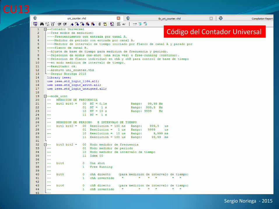
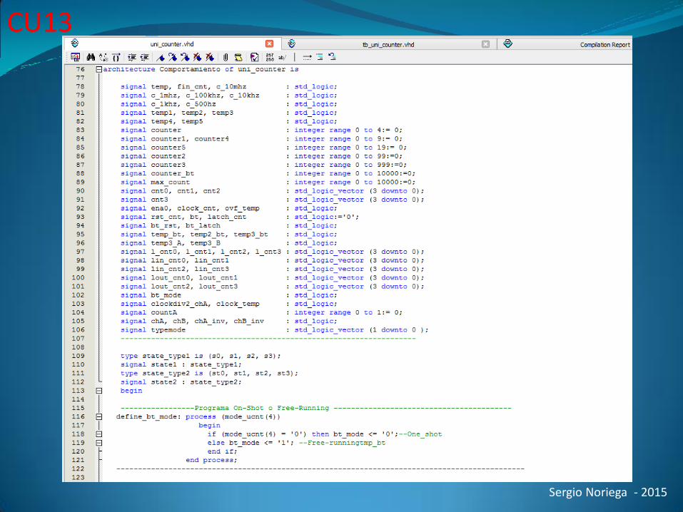
CU13
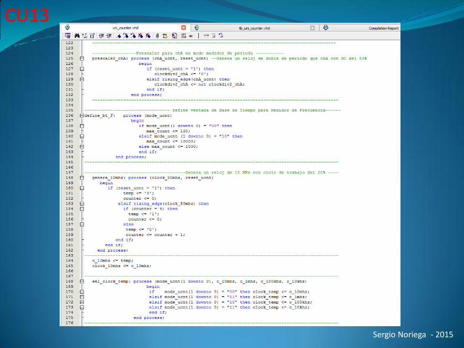
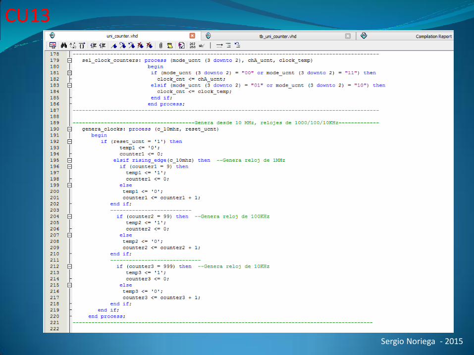
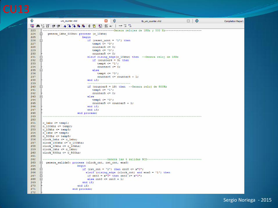
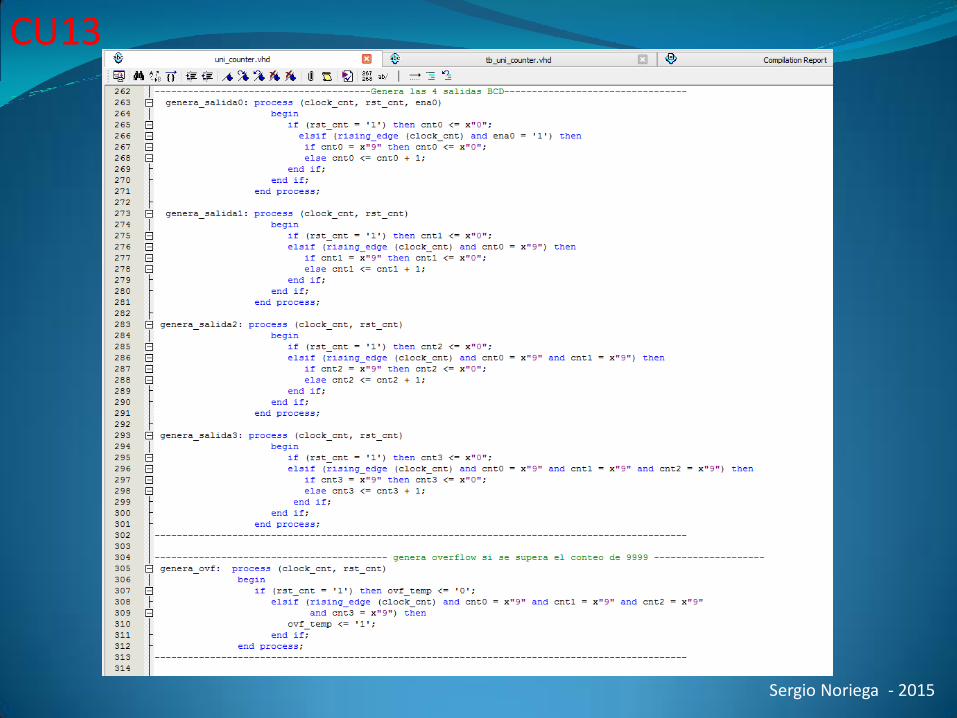
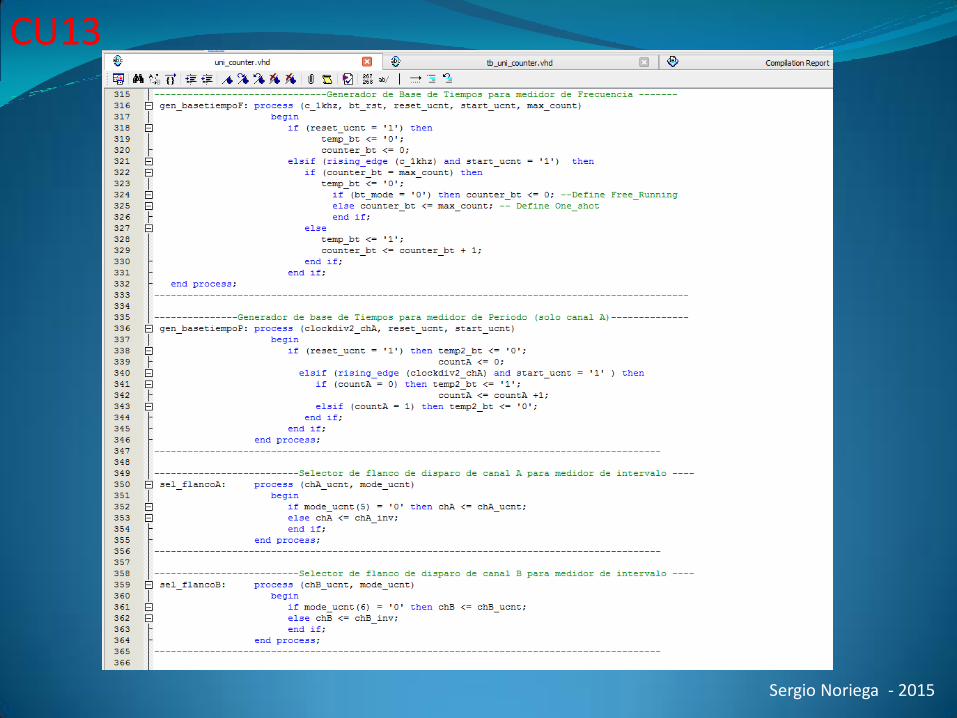
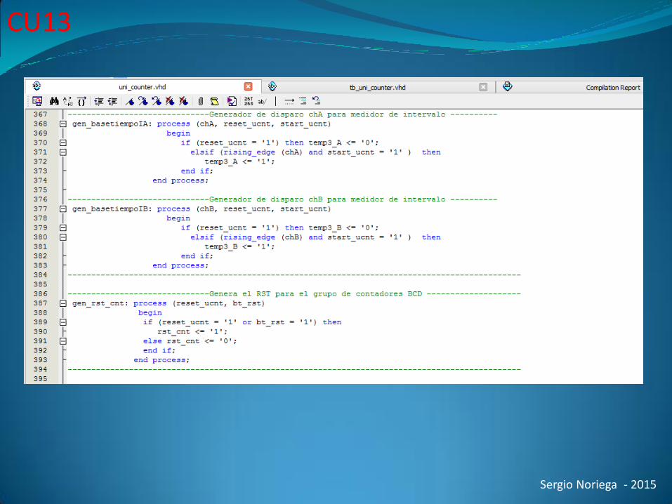
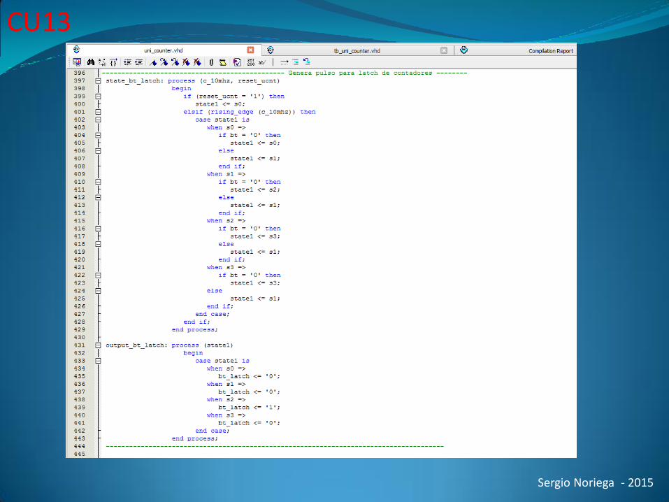
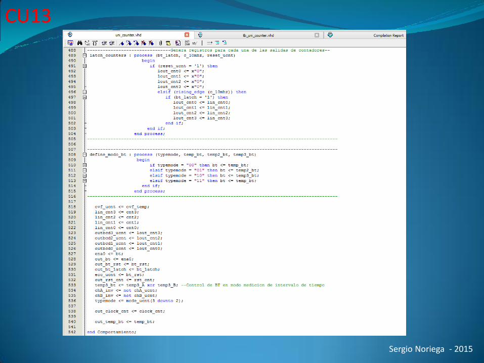
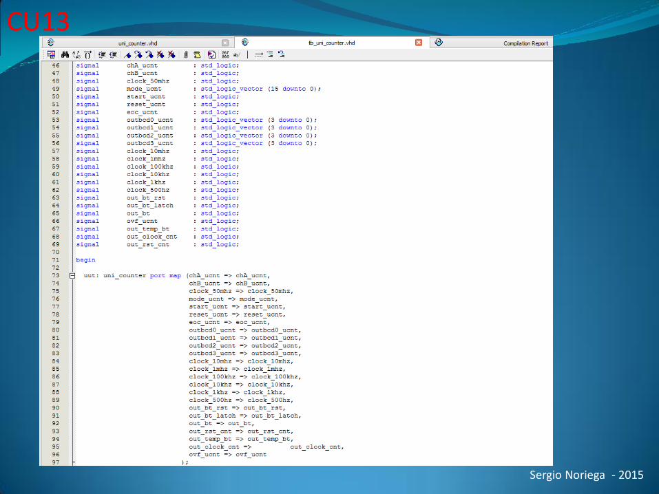
Código del Contador Universal
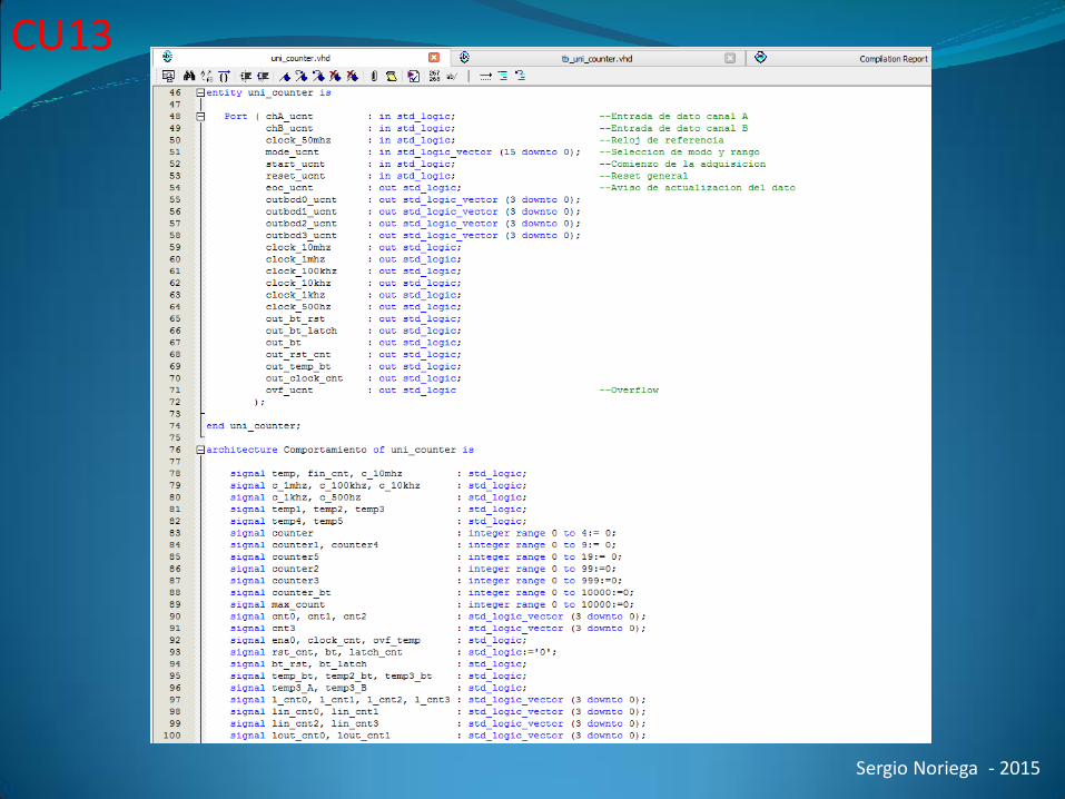
Sergio Noriega - 2015
CU13
Sergio Noriega - 2015
CU13
Sergio Noriega - 2015
CU13
Sergio Noriega - 2015
CU13
Sergio Noriega - 2015
CU13
Sergio Noriega - 2015
CU13
Sergio Noriega - 2015
CU13
Sergio Noriega - 2015
CU13
Sergio Noriega - 2015
CU13

Sergio Noriega - 2015
CU13
Sergio Noriega - 2015
CU13

Sergio Noriega - 2015
CU13
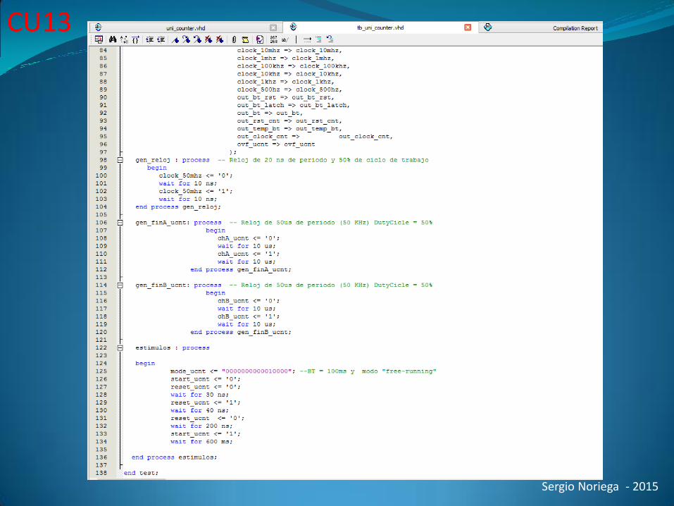
Código del TestBench para el Contador Universal
Sergio Noriega - 2015
CU13
Sergio Noriega - 2015
CU13
Sergio Noriega - 2015
CU13
Sergio Noriega - 2015
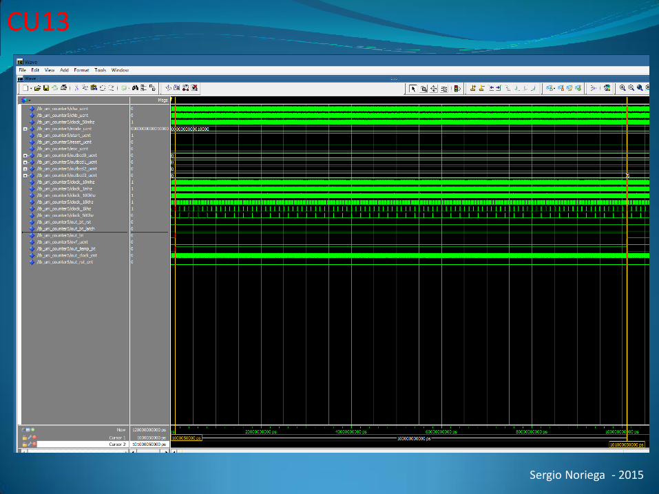
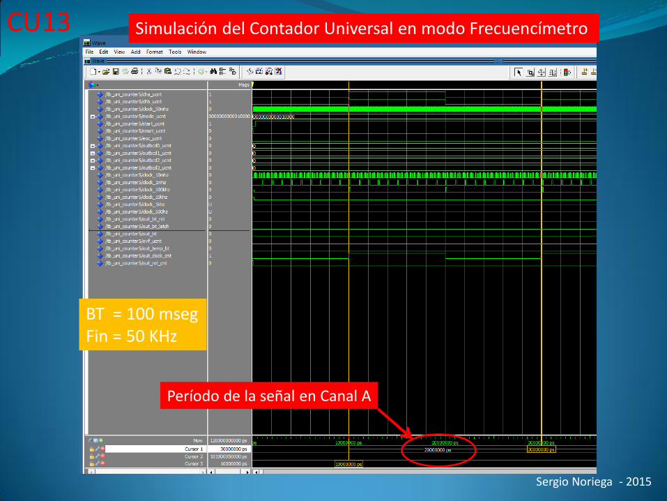
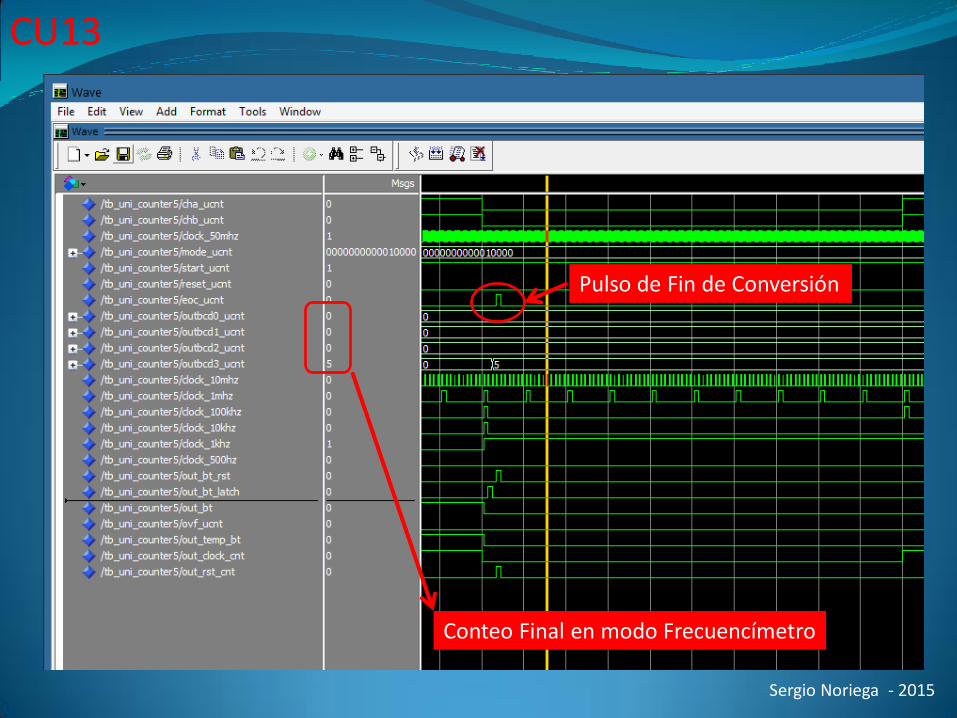
CU13 Simulación del Contador Universal en modo Frecuencímetro
BT = 100 mseg Fin = 50 KHz
Período de la señal en Canal A
Sergio Noriega - 2015
CU13
Pulso de Fin de Conversión
Conteo Final en modo Frecuencímetro
Sergio Noriega - 2015
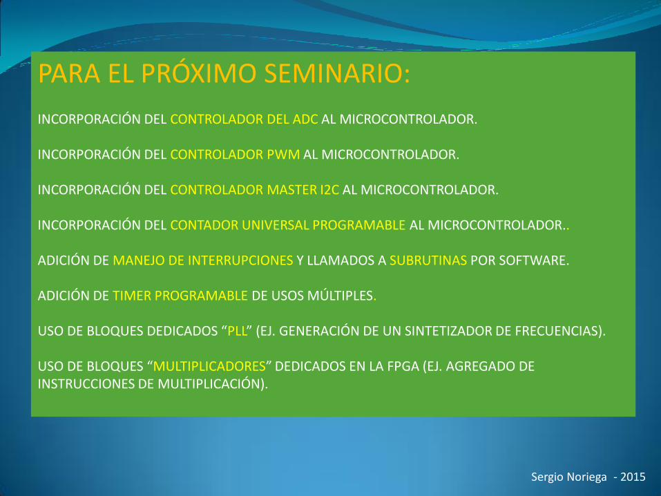
PARA EL PRÓXIMO SEMINARIO: INCORPORACIÓN DEL CONTROLADOR DEL ADC AL MICROCONTROLADOR. INCORPORACIÓN DEL CONTROLADOR PWM AL MICROCONTROLADOR. INCORPORACIÓN DEL CONTROLADOR MASTER I2C AL MICROCONTROLADOR. INCORPORACIÓN DEL CONTADOR UNIVERSAL PROGRAMABLE AL MICROCONTROLADOR.. ADICIÓN DE MANEJO DE INTERRUPCIONES Y LLAMADOS A SUBRUTINAS POR SOFTWARE. ADICIÓN DE TIMER PROGRAMABLE DE USOS MÚLTIPLES. USO DE BLOQUES DEDICADOS “PLL” (EJ. GENERACIÓN DE UN SINTETIZADOR DE FRECUENCIAS). USO DE BLOQUES “MULTIPLICADORES” DEDICADOS EN LA FPGA (EJ. AGREGADO DE INSTRUCCIONES DE MULTIPLICACIÓN).
Sergio Noriega - 2015
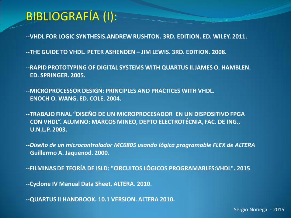
BIBLIOGRAFÍA (I): --VHDL FOR LOGIC SYNTHESIS.ANDREW RUSHTON. 3RD. EDITION. ED. WILEY. 2011. --THE GUIDE TO VHDL. PETER ASHENDEN – JIM LEWIS. 3RD. EDITION. 2008. --RAPID PROTOTYPING OF DIGITAL SYSTEMS WITH QUARTUS II.JAMES O. HAMBLEN. ED. SPRINGER. 2005. --MICROPROCESSOR DESIGN: PRINCIPLES AND PRACTICES WITH VHDL. ENOCH O. WANG. ED. COLE. 2004. --TRABAJO FINAL “DISEÑO DE UN MICROPROCESADOR EN UN DISPOSITIVO FPGA CON VHDL“. ALUMNO: MARCOS MINEO, DEPTO ELECTROTÉCNIA, FAC. DE ING., U.N.L.P. 2003. --Diseño de un microcontrolador MC6805 usando lógica programable FLEX de ALTERA Guillermo A. Jaquenod. 2000. --FILMINAS DE TEORÍA DE ISLD: "CIRCUITOS LÓGICOS PROGRAMABLES:VHDL". 2015 --Cyclone IV Manual Data Sheet. ALTERA. 2010. --QUARTUS II HANDBOOK. 10.1 VERSION. ALTERA 2010.
Sergio Noriega - 2015
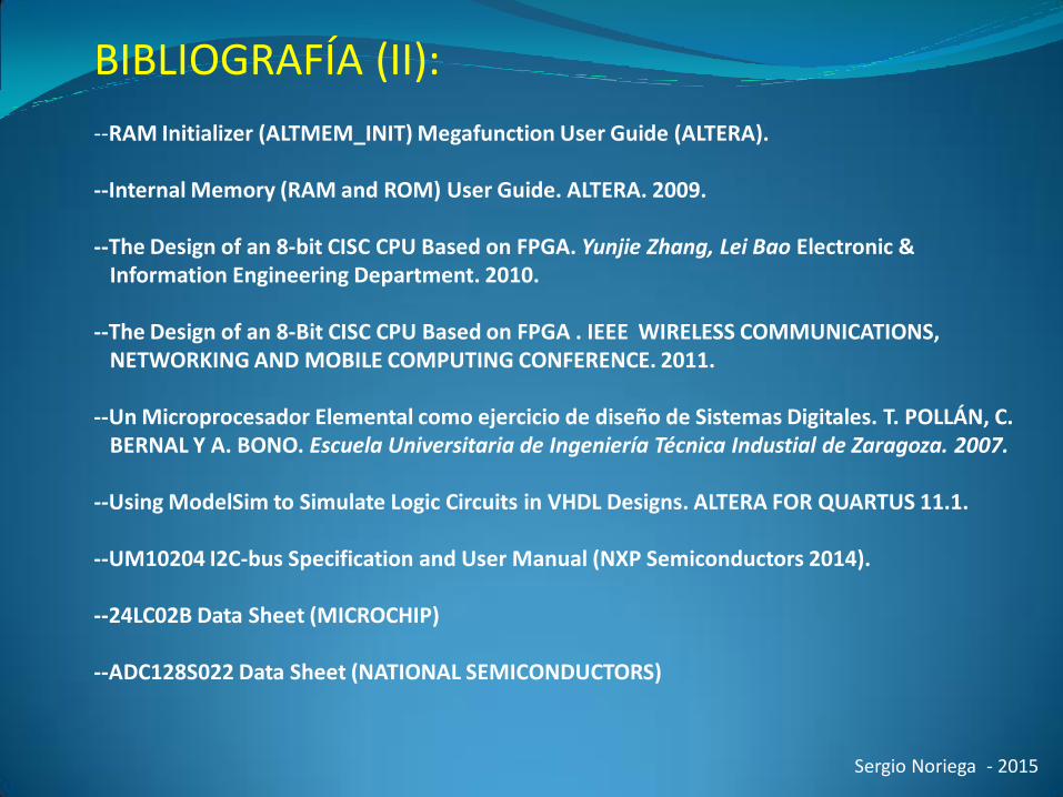
BIBLIOGRAFÍA (II): --RAM Initializer (ALTMEM_INIT) Megafunction User Guide (ALTERA). --Internal Memory (RAM and ROM) User Guide. ALTERA. 2009. --The Design of an 8-bit CISC CPU Based on FPGA. Yunjie Zhang, Lei Bao Electronic & Information Engineering Department. 2010. --The Design of an 8-Bit CISC CPU Based on FPGA . IEEE WIRELESS COMMUNICATIONS, NETWORKING AND MOBILE COMPUTING CONFERENCE. 2011. --Un Microprocesador Elemental como ejercicio de diseño de Sistemas Digitales. T. POLLÁN, C. BERNAL Y A. BONO. Escuela Universitaria de Ingeniería Técnica Industial de Zaragoza. 2007. --Using ModelSim to Simulate Logic Circuits in VHDL Designs. ALTERA FOR QUARTUS 11.1. --UM10204 I2C-bus Specification and User Manual (NXP Semiconductors 2014). --24LC02B Data Sheet (MICROCHIP) --ADC128S022 Data Sheet (NATIONAL SEMICONDUCTORS)
Sergio Noriega - 2015
GRACIAS …