Embed Size (px)
Citation preview
I N V E S T I C E D O R O Z V O J E V Z D Ě L Á V Á N Í
Tato prezentace je spolufinancována Evropským sociálním fondem a státním rozpočtem České republiky.
Mikroprocesorová technika v aplikacích řízení elektrických pohonů
Ing. Jaroslav Lepka
Ing. Pavel Grasblum, Ph.D.
2. – 3. června 2011
2.-3. 6. 2011 1
I N V E S T I C E D O R O Z V O J E V Z D Ě L Á V Á N Í
Agenda
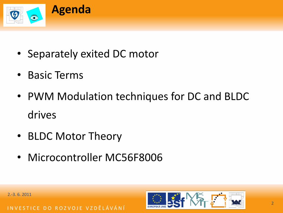
• Separately exited DC motor
• Basic Terms
• PWM Modulation techniques for DC and BLDC
drives
• BLDC Motor Theory
• Microcontroller MC56F8006
2.-3. 6. 2011
2
I N V E S T I C E D O R O Z V O J E V Z D Ě L Á V Á N Í
Agenda
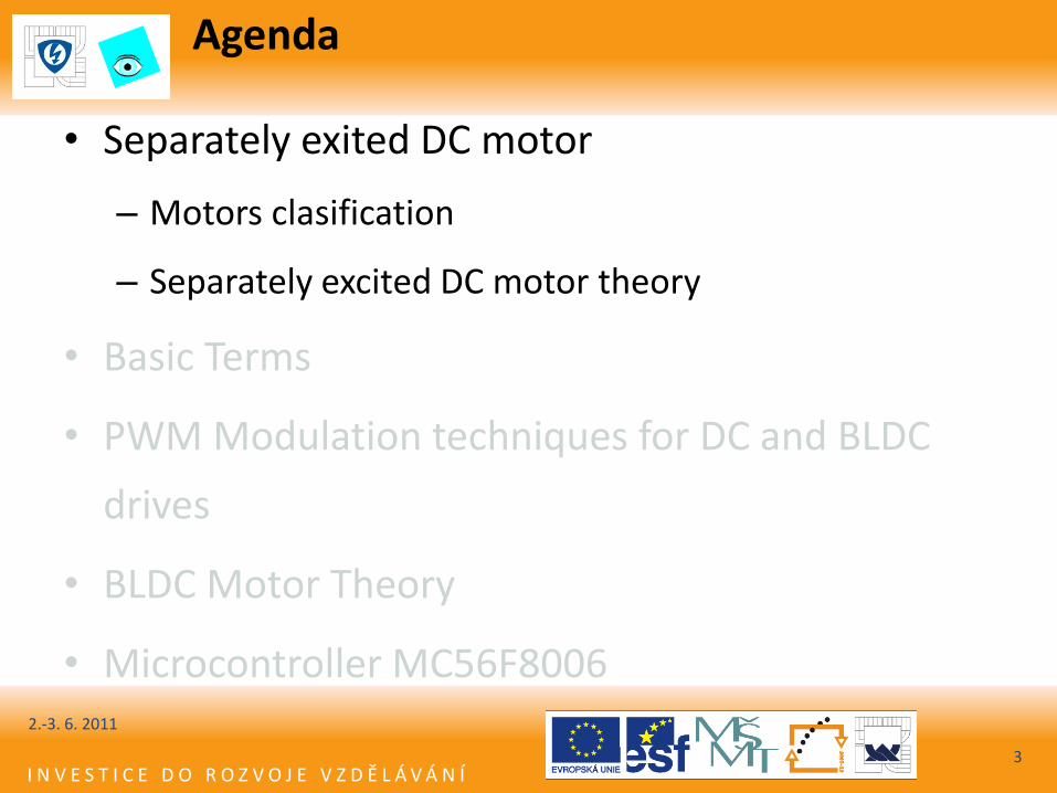
• Separately exited DC motor
– Motors clasification
– Separately excited DC motor theory
• Basic Terms
• PWM Modulation techniques for DC and BLDC
drives
• BLDC Motor Theory
• Microcontroller MC56F8006
2.-3. 6. 2011
3
I N V E S T I C E D O R O Z V O J E V Z D Ě L Á V Á N Í
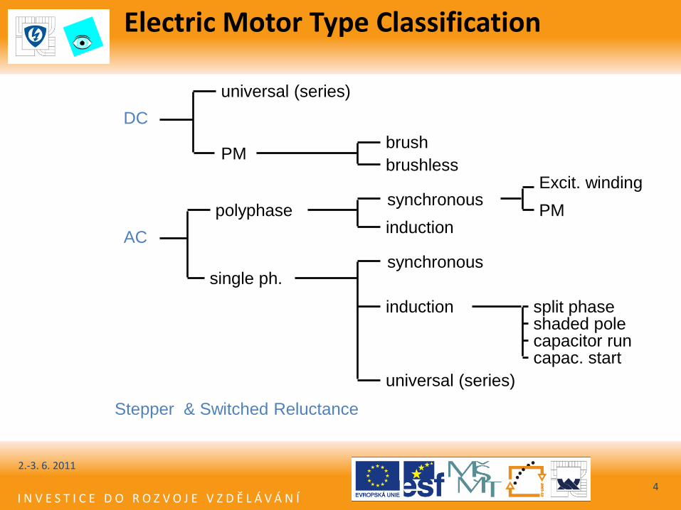
DC
AC
universal (series)
PM brush
brushless
polyphase
single ph.
synchronous
induction
synchronous
PM
induction split phase shaded pole
universal (series)
capacitor run capac. start
Stepper & Switched Reluctance
Excit. winding
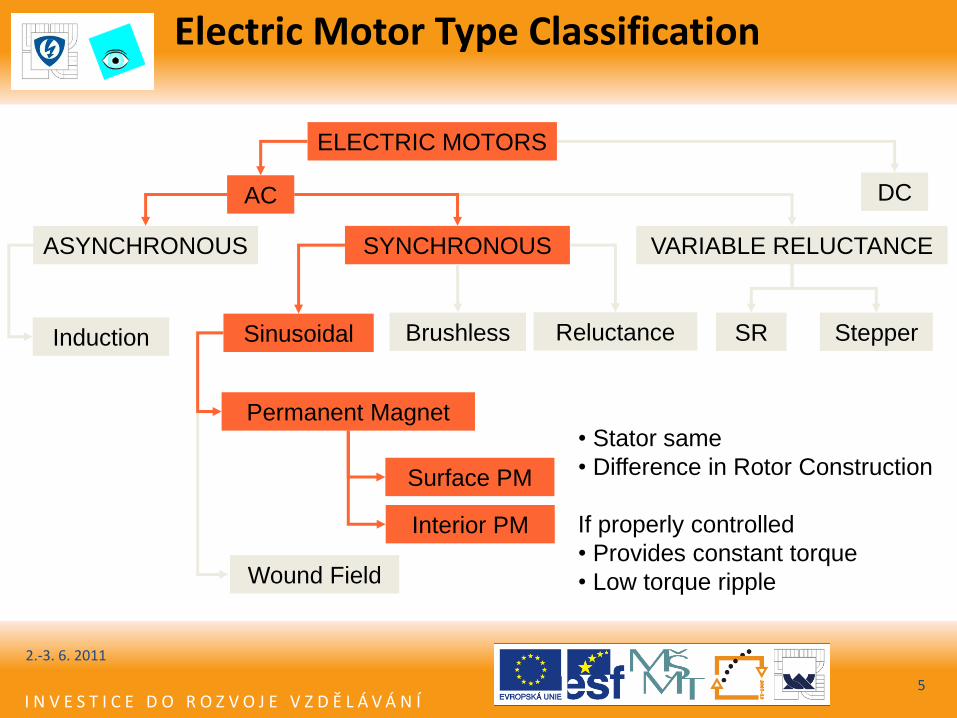
Electric Motor Type Classification
2.-3. 6. 2011
4
I N V E S T I C E D O R O Z V O J E V Z D Ě L Á V Á N Í
Electric Motor Type Classification
5
ELECTRIC MOTORS
AC DC
SYNCHRONOUS ASYNCHRONOUS
Brushless Induction Reluctance Stepper Sinusoidal
Permanent Magnet
Wound Field
Surface PM
Interior PM
• Stator same
• Difference in Rotor Construction
If properly controlled
• Provides constant torque
• Low torque ripple
SR
VARIABLE RELUCTANCE
2.-3. 6. 2011
I N V E S T I C E D O R O Z V O J E V Z D Ě L Á V Á N Í
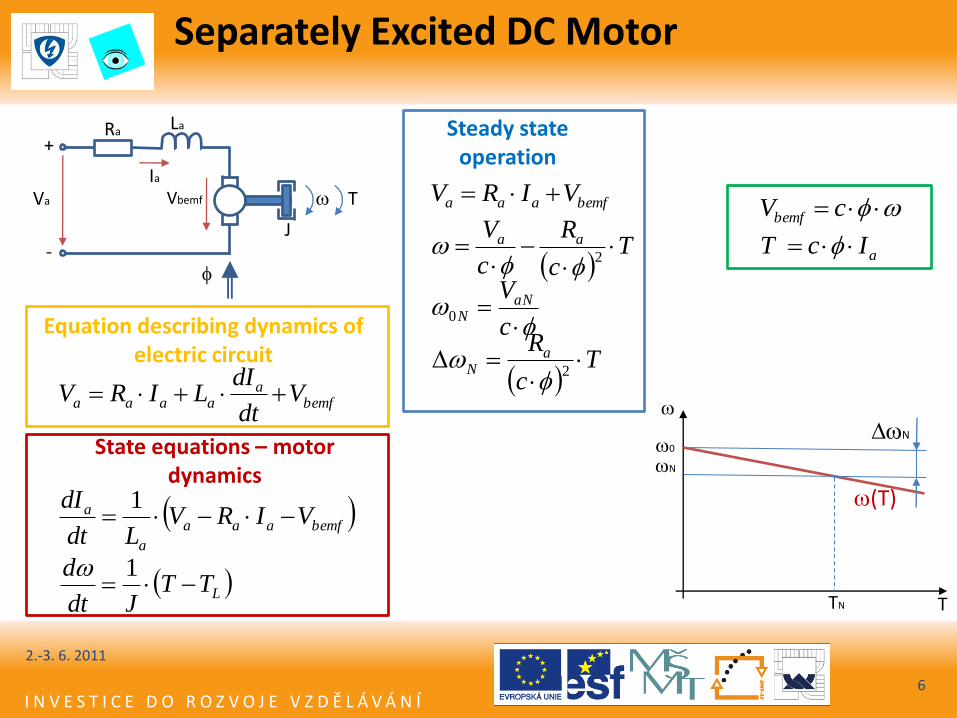
Separately Excited DC Motor
2.-3. 6. 2011
6
T
(T)
0
N
TN
N
La
Va
Ia
Vbemf
Ra
J
T
+
-
bemfaaa VIRV
bemfa
aaaa Vdt
dILIRV
cVbemf
aIcT
Tc
R
c
V aa
2
c
VaNN0
T
c
RaN
2
LTTJdt
d
1
bemfaaa
a
a VIRVLdt
dI
1
Steady state operation
State equations – motor dynamics
Equation describing dynamics of electric circuit
I N V E S T I C E D O R O Z V O J E V Z D Ě L Á V Á N Í
Agenda
2.-3. 6. 2011
7
• Separately exited DC motor
• Basic Terms
– Operational Characteristic of the Drive
– Unipolar versus Bipolar Switching
– Independent versus Complementary Switching
– Edge versus Centre Aligned PWM
• PWM Modulation techniques for DC and BLDC drives
• BLDC Motor Theory
• Microcontroller MC56F8006
I N V E S T I C E D O R O Z V O J E V Z D Ě L Á V Á N Í
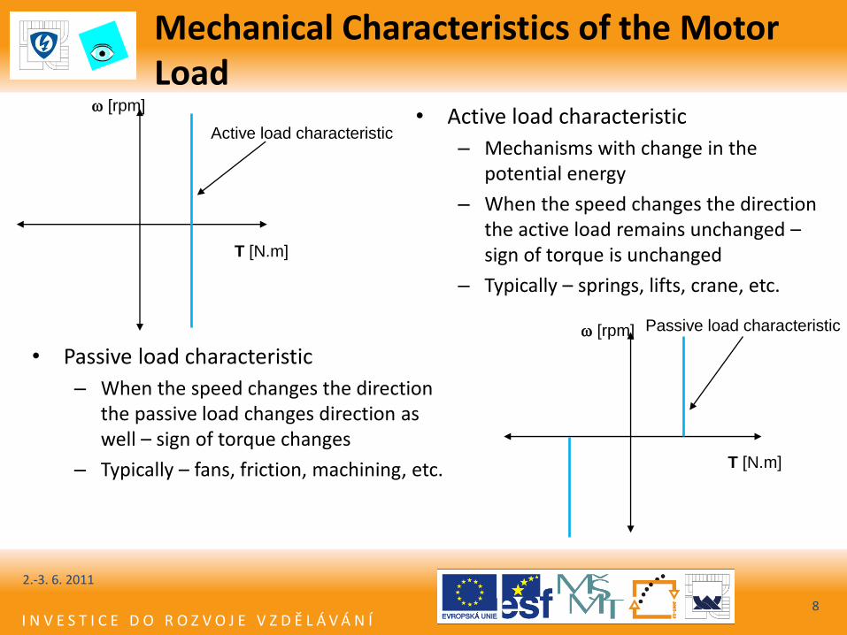
Mechanical Characteristics of the Motor Load
2.-3. 6. 2011
8
• Active load characteristic
– Mechanisms with change in the potential energy
– When the speed changes the direction the active load remains unchanged – sign of torque is unchanged
– Typically – springs, lifts, crane, etc.
T [N.m]
[rpm]
Active load characteristic
Passive load characteristic
T [N.m]
[rpm]
• Passive load characteristic
– When the speed changes the direction the passive load changes direction as well – sign of torque changes
– Typically – fans, friction, machining, etc.
I N V E S T I C E D O R O Z V O J E V Z D Ě L Á V Á N Í
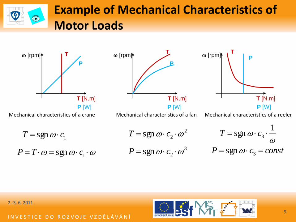
Example of Mechanical Characteristics of Motor Loads
2.-3. 6. 2011
9
T [N.m]
[rpm]
P [W]
T
P
Mechanical characteristics of a crane
1sgn cT
1sgn cTP
T [N.m]
[rpm]
P [W]
T
P
Mechanical characteristics of a fan
2
2sgn cT
3
2sgn cP
T [N.m]
[rpm]
P [W]
T P
Mechanical characteristics of a reeler
1sgn 3 cT
constcP 3sgn
I N V E S T I C E D O R O Z V O J E V Z D Ě L Á V Á N Í
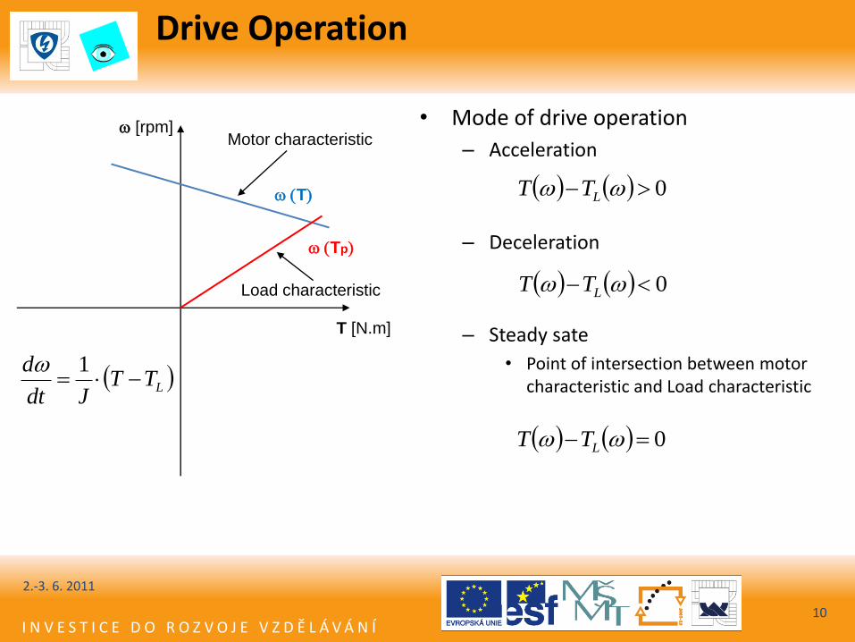
Drive Operation
2.-3. 6. 2011
10
• Mode of drive operation
– Acceleration
– Deceleration
– Steady sate
• Point of intersection between motor characteristic and Load characteristic
T [N.m]
[rpm]
Load characteristic
Motor characteristic
T
Tp
LTTJdt
d
1
0 LTT
0 LTT
0 LTT
I N V E S T I C E D O R O Z V O J E V Z D Ě L Á V Á N Í
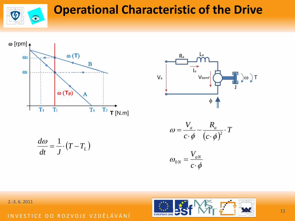
Operational Characteristic of the Drive
2.-3. 6. 2011
11
T [N.m]
[rpm]
T
Tp
LTTJdt
d
1
2
1
T1 T2 TS T3
B
A
Va
Ia
Vbemf
Ra La
J
T
T
c
R
c
V aa
2
c
VaNN0
I N V E S T I C E D O R O Z V O J E V Z D Ě L Á V Á N Í
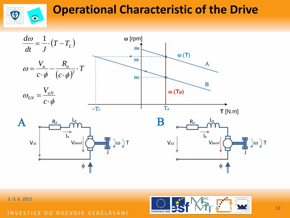
Operational Characteristic of the Drive
2.-3. 6. 2011
12
T [N.m]
[rpm]
T
Tp
LTTJdt
d
1
1
2
Tp T2
B
A
Va1
Ia
Vbemf
Ra La
J
T
T
c
R
c
V aa
2
c
VaNN0
0
Va2
Ia
Vbemf
Ra La
J
T
B
A
I N V E S T I C E D O R O Z V O J E V Z D Ě L Á V Á N Í
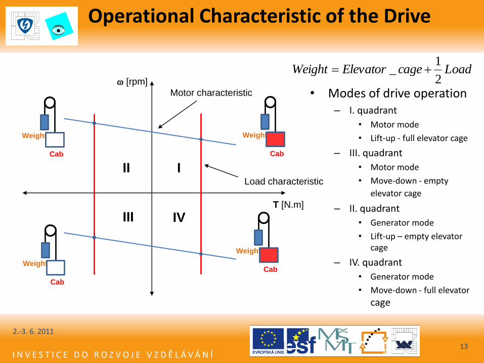
Operational Characteristic of the Drive
2.-3. 6. 2011
13
• Modes of drive operation – I. quadrant
• Motor mode
• Lift-up - full elevator cage
– III. quadrant
• Motor mode
• Move-down - empty
elevator cage
– II. quadrant
• Generator mode
• Lift-up – empty elevator cage
– IV. quadrant
• Generator mode
• Move-down - full elevator
cage
T [N.m]
[rpm]
Load characteristic
Motor characteristic
Weight
Cab
Weight
Cab
Weight
Cab
Weight
Cab
I II
III IV
LoadcageElevatorWeight2
1_
I N V E S T I C E D O R O Z V O J E V Z D Ě L Á V Á N Í
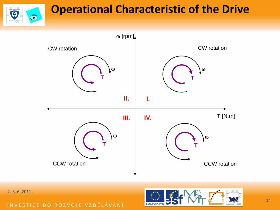
Operational Characteristic of the Drive
2.-3. 6. 2011
14
T [N.m]
[rpm]
CW rotation
T
T
T
T
CW rotation
CCW rotation
I. II.
III. IV.
CCW rotation
I N V E S T I C E D O R O Z V O J E V Z D Ě L Á V Á N Í
Operational Characteristic of the Drive
2.-3. 6. 2011
15
• Single Quadrant Operation
T [N.m]
[rpm]
CW rotation
T
T
T
T
CW rotation
CCW rotation
I. II.
III. IV.
CCW rotation
I N V E S T I C E D O R O Z V O J E V Z D Ě L Á V Á N Í
Operational Characteristic of the Drive
2.-3. 6. 2011
16
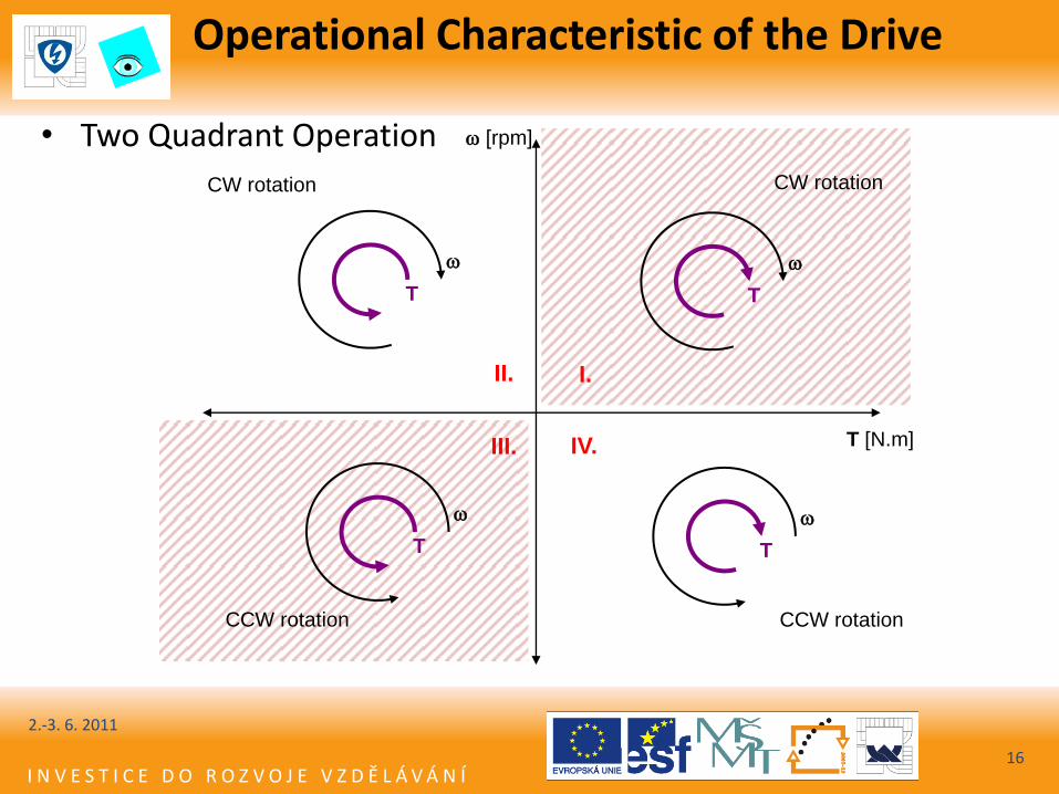
• Two Quadrant Operation
T [N.m]
[rpm]
CW rotation
T
T
T
T
CW rotation
CCW rotation
I. II.
III. IV.
CCW rotation
I N V E S T I C E D O R O Z V O J E V Z D Ě L Á V Á N Í
Operational Characteristic of the Drive
2.-3. 6. 2011
17
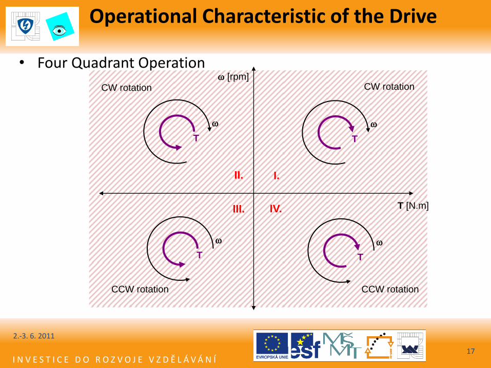
• Four Quadrant Operation
T [N.m]
[rpm] CW rotation
T
T
T
T
CW rotation
CCW rotation
I. II.
III. IV.
CCW rotation
I N V E S T I C E D O R O Z V O J E V Z D Ě L Á V Á N Í
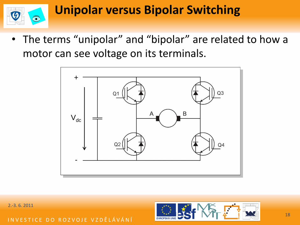
Unipolar versus Bipolar Switching
2.-3. 6. 2011
18
• The terms “unipolar” and “bipolar” are related to how a motor can see voltage on its terminals.
+
-
Vdc
I N V E S T I C E D O R O Z V O J E V Z D Ě L Á V Á N Í
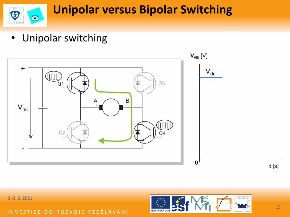
Unipolar versus Bipolar Switching
2.-3. 6. 2011
19
• Unipolar switching
t [s]
VAB [V]
0
+
-
Vdc
Vdc
I N V E S T I C E D O R O Z V O J E V Z D Ě L Á V Á N Í
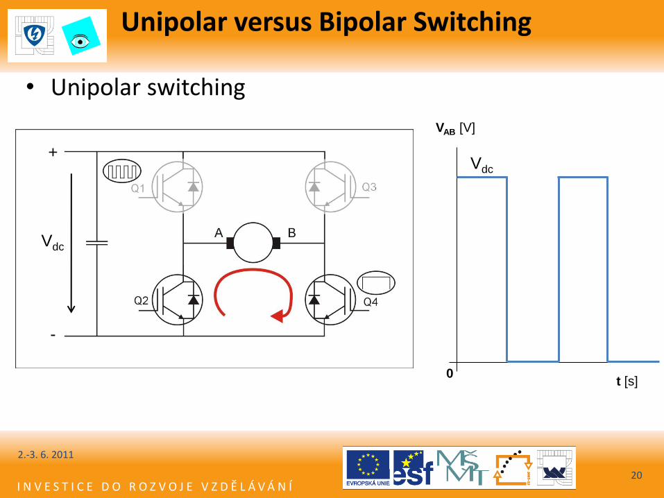
Unipolar versus Bipolar Switching
2.-3. 6. 2011
20
• Unipolar switching
t [s]
VAB [V]
0
+
-
Vdc
Vdc
I N V E S T I C E D O R O Z V O J E V Z D Ě L Á V Á N Í
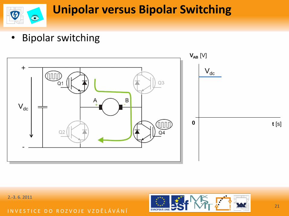
Unipolar versus Bipolar Switching
2.-3. 6. 2011
21
• Bipolar switching
VAB [V]
t [s] 0
+
-
Vdc
Vdc
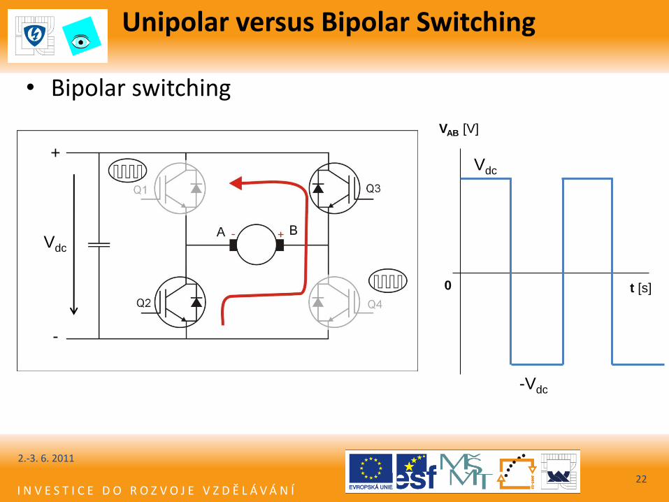
I N V E S T I C E D O R O Z V O J E V Z D Ě L Á V Á N Í
Unipolar versus Bipolar Switching
2.-3. 6. 2011
22
• Bipolar switching
t [s]
VAB [V]
0
+
-
Vdc
Vdc
-Vdc
I N V E S T I C E D O R O Z V O J E V Z D Ě L Á V Á N Í
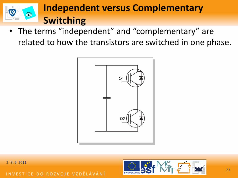
Independent versus Complementary Switching
2.-3. 6. 2011
23
• The terms “independent” and “complementary” are related to how the transistors are switched in one phase.
I N V E S T I C E D O R O Z V O J E V Z D Ě L Á V Á N Í
Independent versus Complementary Switching
2.-3. 6. 2011
24
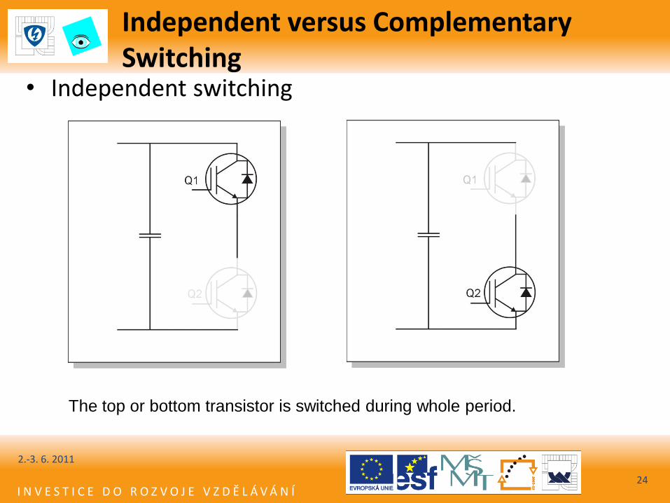
• Independent switching
The top or bottom transistor is switched during whole period.
I N V E S T I C E D O R O Z V O J E V Z D Ě L Á V Á N Í
Independent versus Complementary Switching
2.-3. 6. 2011
25
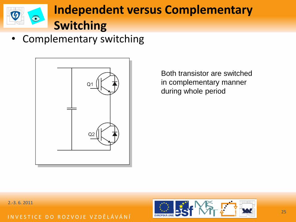
• Complementary switching
Both transistor are switched
in complementary manner
during whole period
I N V E S T I C E D O R O Z V O J E V Z D Ě L Á V Á N Í
Edge versus Center Aligned PWM
2.-3. 6. 2011
26
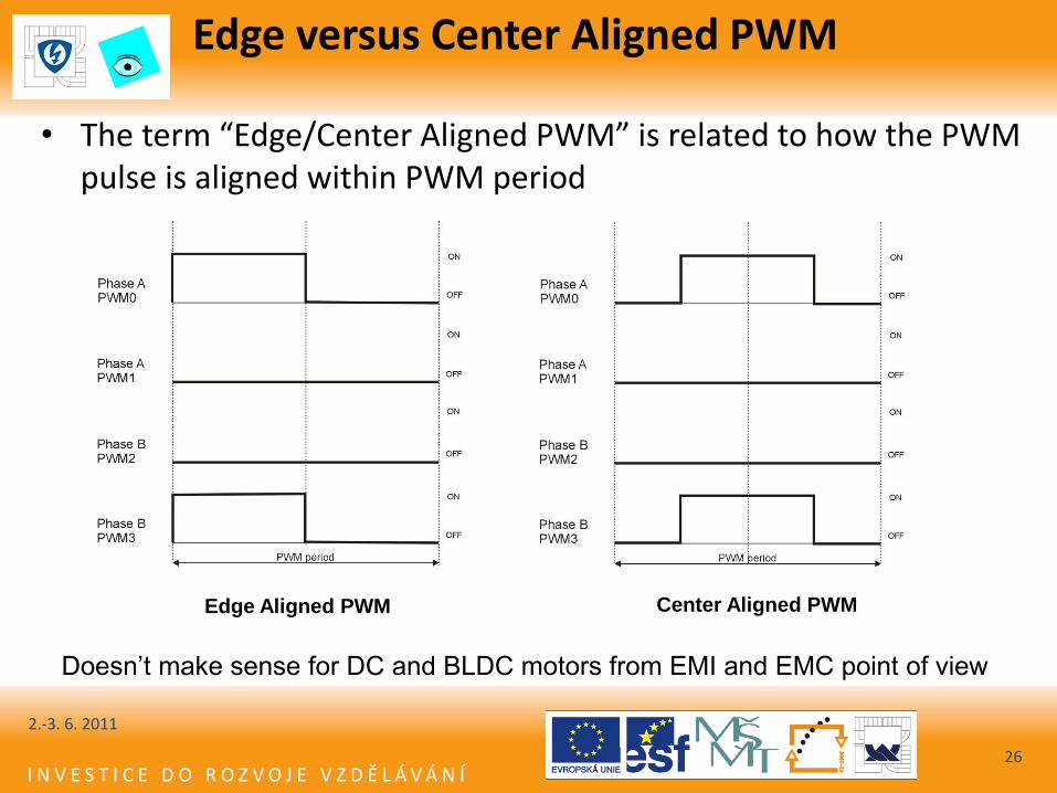
• The term “Edge/Center Aligned PWM” is related to how the PWM pulse is aligned within PWM period
Edge Aligned PWM Center Aligned PWM
Doesn’t make sense for DC and BLDC motors from EMI and EMC point of view
I N V E S T I C E D O R O Z V O J E V Z D Ě L Á V Á N Í
Edge versus Center Aligned PWM
2.-3. 6. 2011
27
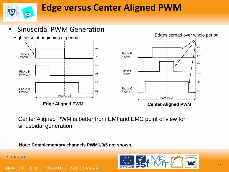
• Sinusoidal PWM Generation
Edge Aligned PWM Center Aligned PWM
Center Aligned PWM is better from EMI and EMC point of view for
sinusoidal generation
Note: Complementary channels PWM1/3/5 not shown.
Edges spread over whole period High noise at beginning of period
I N V E S T I C E D O R O Z V O J E V Z D Ě L Á V Á N Í
Agenda
2.-3. 6. 2011
28
• Separately exited DC motor
• Basic Terms
• PWM Modulation techniques for DC and BLDC drives
– DC Motors – Single Quadrant Operation
• Single Switch and Freewheeling Diode
– DC and BLDC Motors – 2 & 4 Quadrant Operation
• H-Bridge & 3-Phase Bridge
• Independent Bipolar Switching
• Independent Unipolar Switching
• Complementary Bipolar Switching
• Complementary Unipolar Switching
• Independent/Complementary Unipolar Switching
• BLDC Motor Theory
• Microcontroller MC56F8006
I N V E S T I C E D O R O Z V O J E V Z D Ě L Á V Á N Í
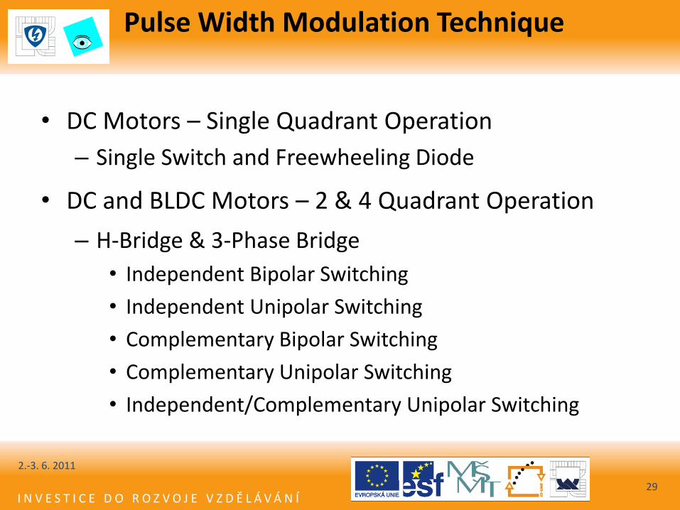
Pulse Width Modulation Technique
• DC Motors – Single Quadrant Operation
– Single Switch and Freewheeling Diode
• DC and BLDC Motors – 2 & 4 Quadrant Operation
– H-Bridge & 3-Phase Bridge
• Independent Bipolar Switching
• Independent Unipolar Switching
• Complementary Bipolar Switching
• Complementary Unipolar Switching
• Independent/Complementary Unipolar Switching
2.-3. 6. 2011
29
I N V E S T I C E D O R O Z V O J E V Z D Ě L Á V Á N Í
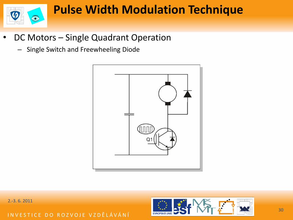
Pulse Width Modulation Technique
30
• DC Motors – Single Quadrant Operation – Single Switch and Freewheeling Diode
2.-3. 6. 2011
I N V E S T I C E D O R O Z V O J E V Z D Ě L Á V Á N Í
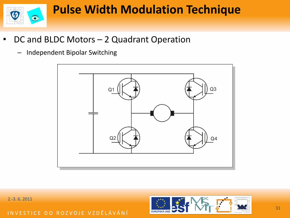
Pulse Width Modulation Technique
31
• DC and BLDC Motors – 2 Quadrant Operation
– Independent Bipolar Switching
2.-3. 6. 2011

I N V E S T I C E D O R O Z V O J E V Z D Ě L Á V Á N Í
Pulse Width Modulation Technique
32
• DC and BLDC Motors – 2 Quadrant Operation
– Independent Bipolar Switching – Acting Transistors
Q1=Q4=PWM
2.-3. 6. 2011
I N V E S T I C E D O R O Z V O J E V Z D Ě L Á V Á N Í
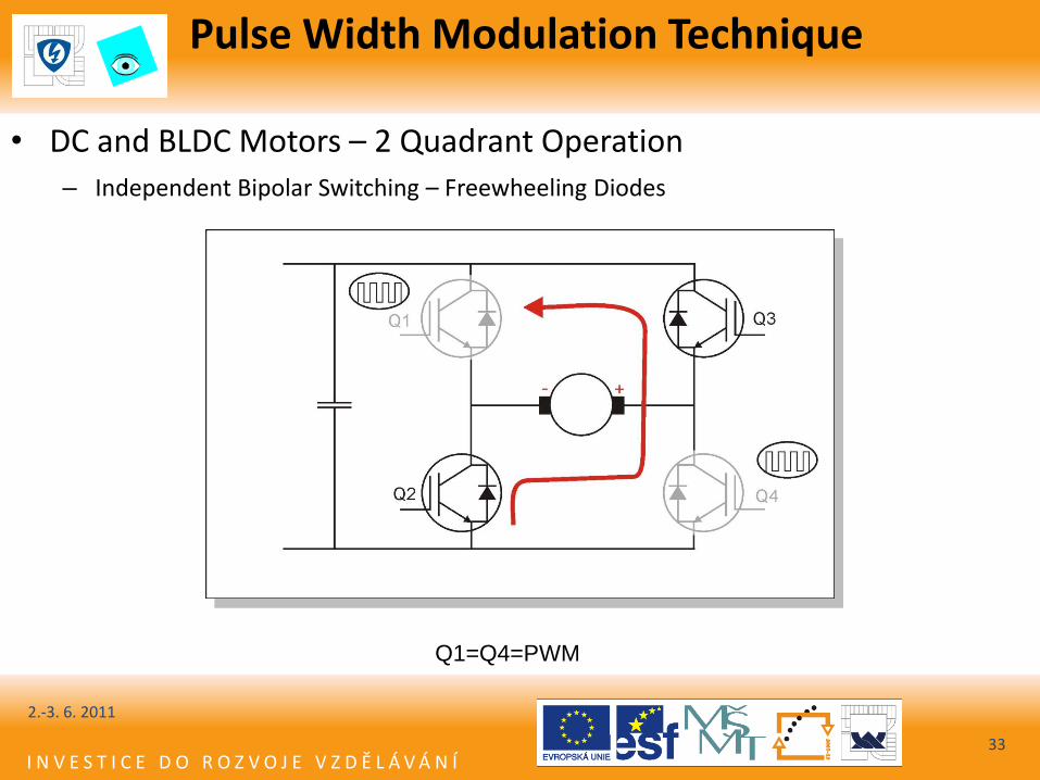
Pulse Width Modulation Technique
33
• DC and BLDC Motors – 2 Quadrant Operation
– Independent Bipolar Switching – Freewheeling Diodes
Q1=Q4=PWM
2.-3. 6. 2011
I N V E S T I C E D O R O Z V O J E V Z D Ě L Á V Á N Í
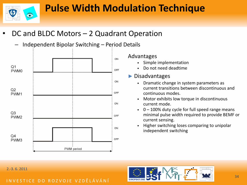
Pulse Width Modulation Technique
34
• DC and BLDC Motors – 2 Quadrant Operation
– Independent Bipolar Switching – Period Details
Advantages
• Simple implementation • Do not need deadtime
► Disadvantages • Dramatic change in system parameters as
current transitions between discontinuous and continuous modes.
• Motor exhibits low torque in discontinuous current mode.
• 0 – 100% duty cycle for full speed range means minimal pulse width required to provide BEMF or current sensing.
• Higher switching loses comparing to unipolar independent switching
2.-3. 6. 2011
I N V E S T I C E D O R O Z V O J E V Z D Ě L Á V Á N Í
Pulse Width Modulation Technique
35
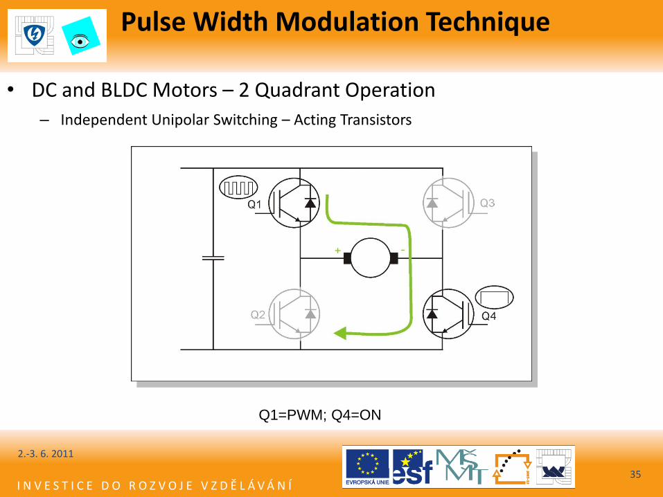
• DC and BLDC Motors – 2 Quadrant Operation
– Independent Unipolar Switching – Acting Transistors
Q1=PWM; Q4=ON
2.-3. 6. 2011
I N V E S T I C E D O R O Z V O J E V Z D Ě L Á V Á N Í
Pulse Width Modulation Technique
36
• DC and BLDC Motors – 2 Quadrant Operation
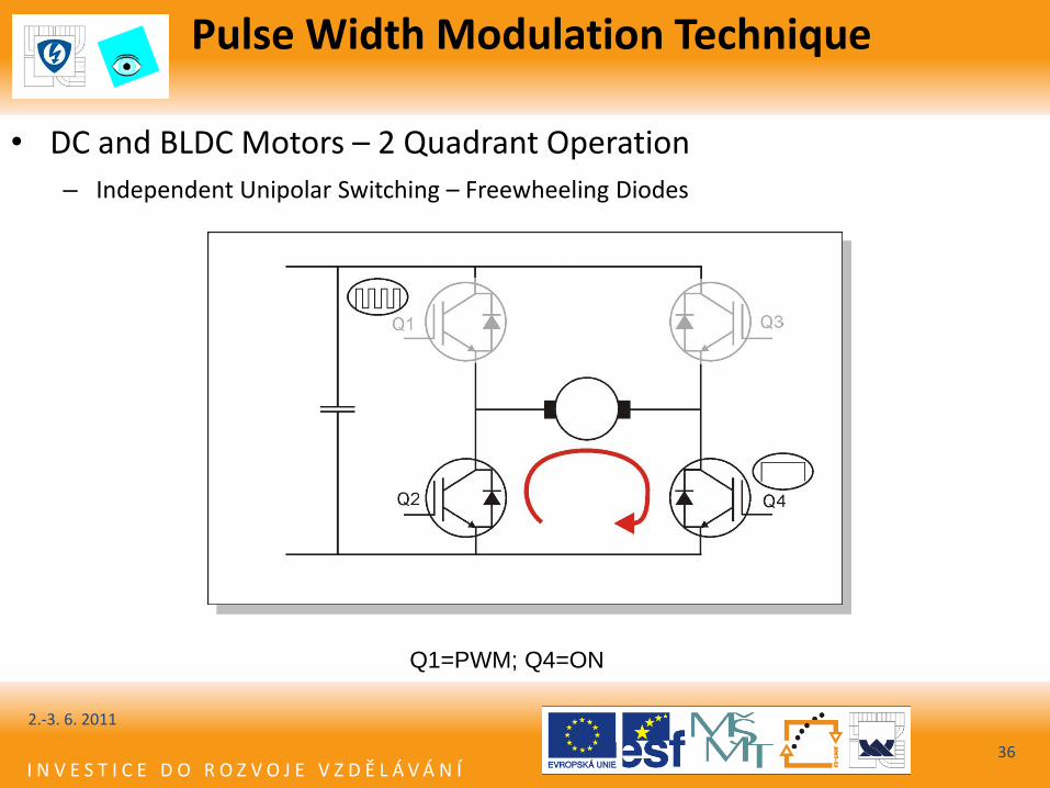
– Independent Unipolar Switching – Freewheeling Diodes
Q1=PWM; Q4=ON
2.-3. 6. 2011
I N V E S T I C E D O R O Z V O J E V Z D Ě L Á V Á N Í
Pulse Width Modulation Technique
37
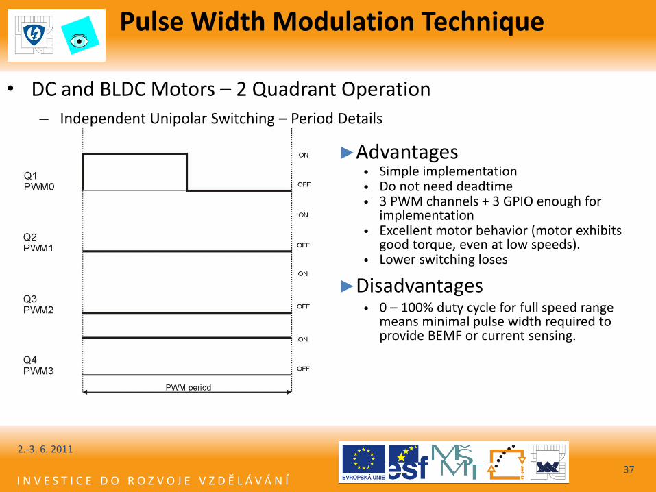
• DC and BLDC Motors – 2 Quadrant Operation
– Independent Unipolar Switching – Period Details
►Advantages
• Simple implementation • Do not need deadtime • 3 PWM channels + 3 GPIO enough for
implementation • Excellent motor behavior (motor exhibits
good torque, even at low speeds). • Lower switching loses
►Disadvantages • 0 – 100% duty cycle for full speed range
means minimal pulse width required to provide BEMF or current sensing.
2.-3. 6. 2011
I N V E S T I C E D O R O Z V O J E V Z D Ě L Á V Á N Í
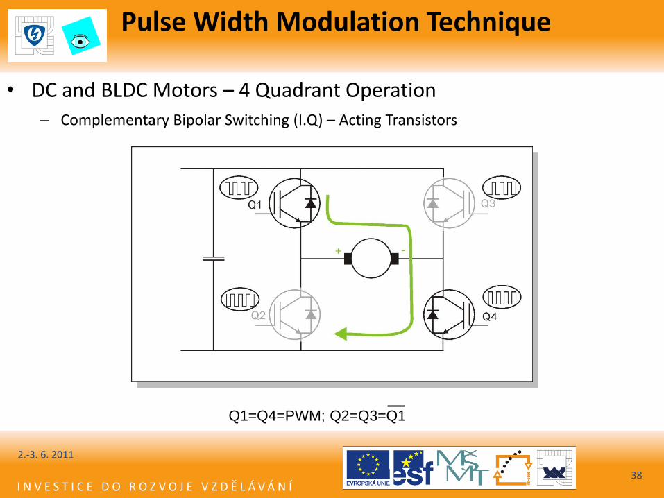
Pulse Width Modulation Technique
38
• DC and BLDC Motors – 4 Quadrant Operation
– Complementary Bipolar Switching (I.Q) – Acting Transistors
Q1=Q4=PWM; Q2=Q3=Q1
2.-3. 6. 2011
I N V E S T I C E D O R O Z V O J E V Z D Ě L Á V Á N Í
Pulse Width Modulation Technique
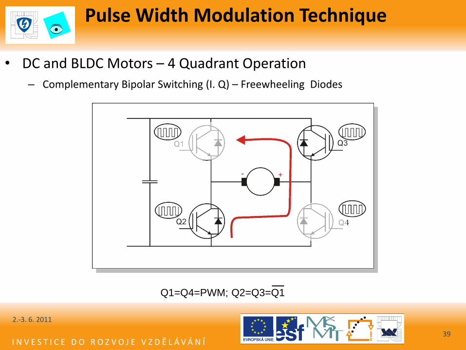
39
• DC and BLDC Motors – 4 Quadrant Operation
– Complementary Bipolar Switching (I. Q) – Freewheeling Diodes
Q1=Q4=PWM; Q2=Q3=Q1
2.-3. 6. 2011
I N V E S T I C E D O R O Z V O J E V Z D Ě L Á V Á N Í
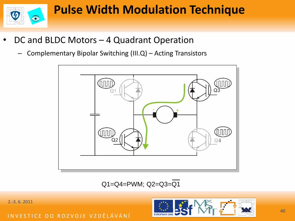
Pulse Width Modulation Technique
40
• DC and BLDC Motors – 4 Quadrant Operation
– Complementary Bipolar Switching (III.Q) – Acting Transistors
Q1=Q4=PWM; Q2=Q3=Q1
2.-3. 6. 2011
I N V E S T I C E D O R O Z V O J E V Z D Ě L Á V Á N Í
Pulse Width Modulation Technique
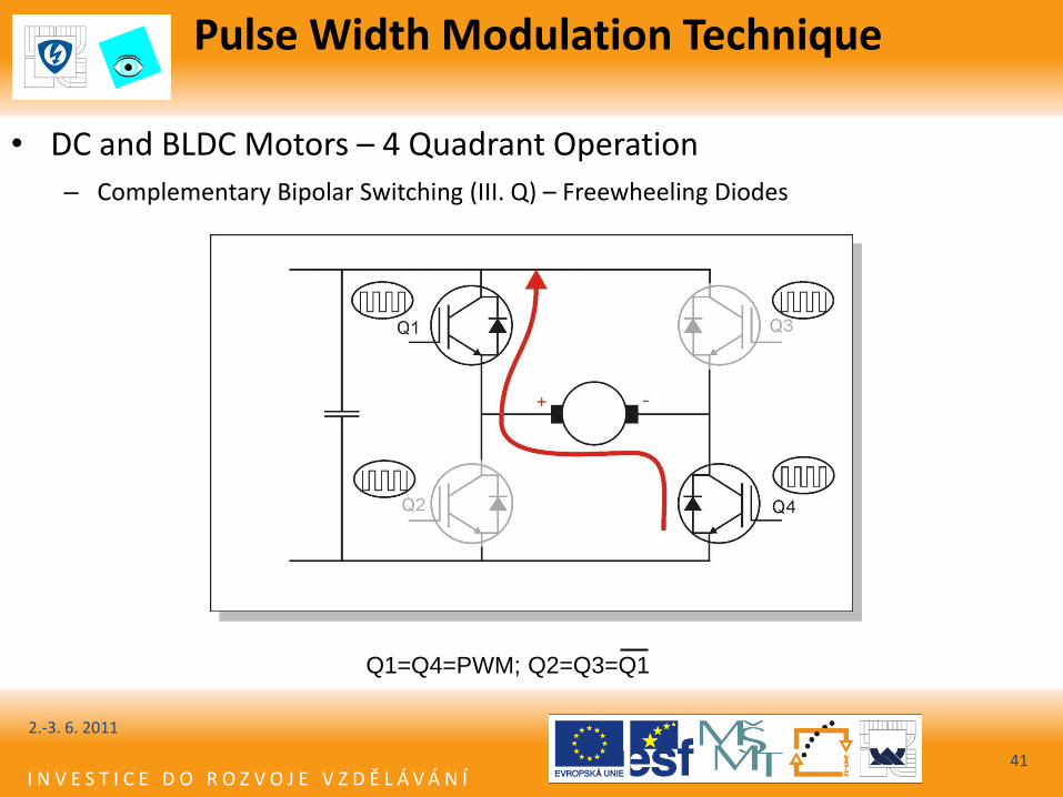
41
• DC and BLDC Motors – 4 Quadrant Operation
– Complementary Bipolar Switching (III. Q) – Freewheeling Diodes
Q1=Q4=PWM; Q2=Q3=Q1
2.-3. 6. 2011
I N V E S T I C E D O R O Z V O J E V Z D Ě L Á V Á N Í
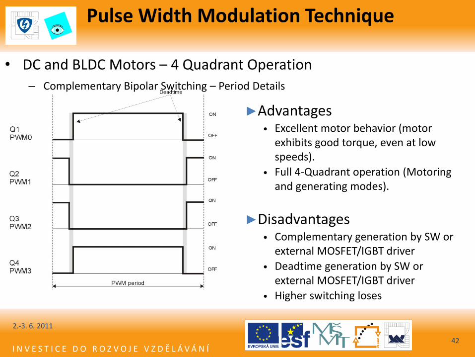
Pulse Width Modulation Technique
42
• DC and BLDC Motors – 4 Quadrant Operation
– Complementary Bipolar Switching – Period Details
►Advantages
• Excellent motor behavior (motor exhibits good torque, even at low speeds).
• Full 4-Quadrant operation (Motoring and generating modes).
►Disadvantages • Complementary generation by SW or
external MOSFET/IGBT driver
• Deadtime generation by SW or external MOSFET/IGBT driver
• Higher switching loses
2.-3. 6. 2011
I N V E S T I C E D O R O Z V O J E V Z D Ě L Á V Á N Í
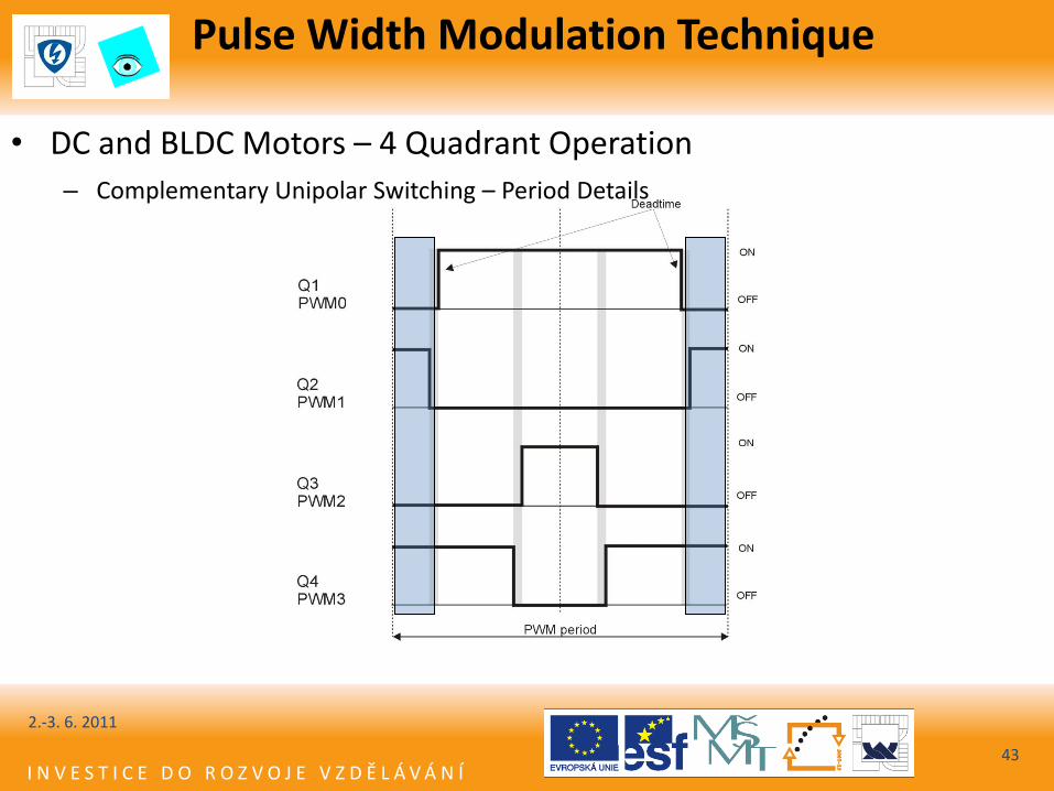
Pulse Width Modulation Technique
43
• DC and BLDC Motors – 4 Quadrant Operation
– Complementary Unipolar Switching – Period Details
2.-3. 6. 2011
I N V E S T I C E D O R O Z V O J E V Z D Ě L Á V Á N Í
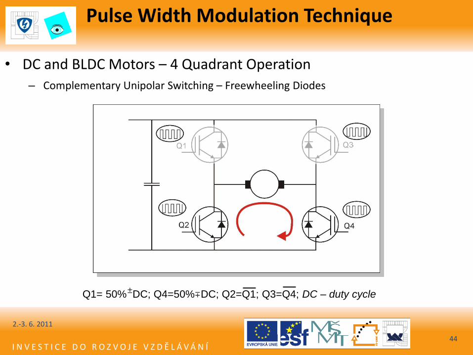
Pulse Width Modulation Technique
44
• DC and BLDC Motors – 4 Quadrant Operation
– Complementary Unipolar Switching – Freewheeling Diodes
Q1= 50% DC; Q4=50% DC; Q2=Q1; Q3=Q4; DC – duty cycle ± ±
2.-3. 6. 2011
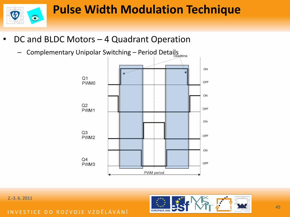
I N V E S T I C E D O R O Z V O J E V Z D Ě L Á V Á N Í
Pulse Width Modulation Technique
45
• DC and BLDC Motors – 4 Quadrant Operation
– Complementary Unipolar Switching – Period Details
2.-3. 6. 2011
I N V E S T I C E D O R O Z V O J E V Z D Ě L Á V Á N Í
Pulse Width Modulation Technique
46
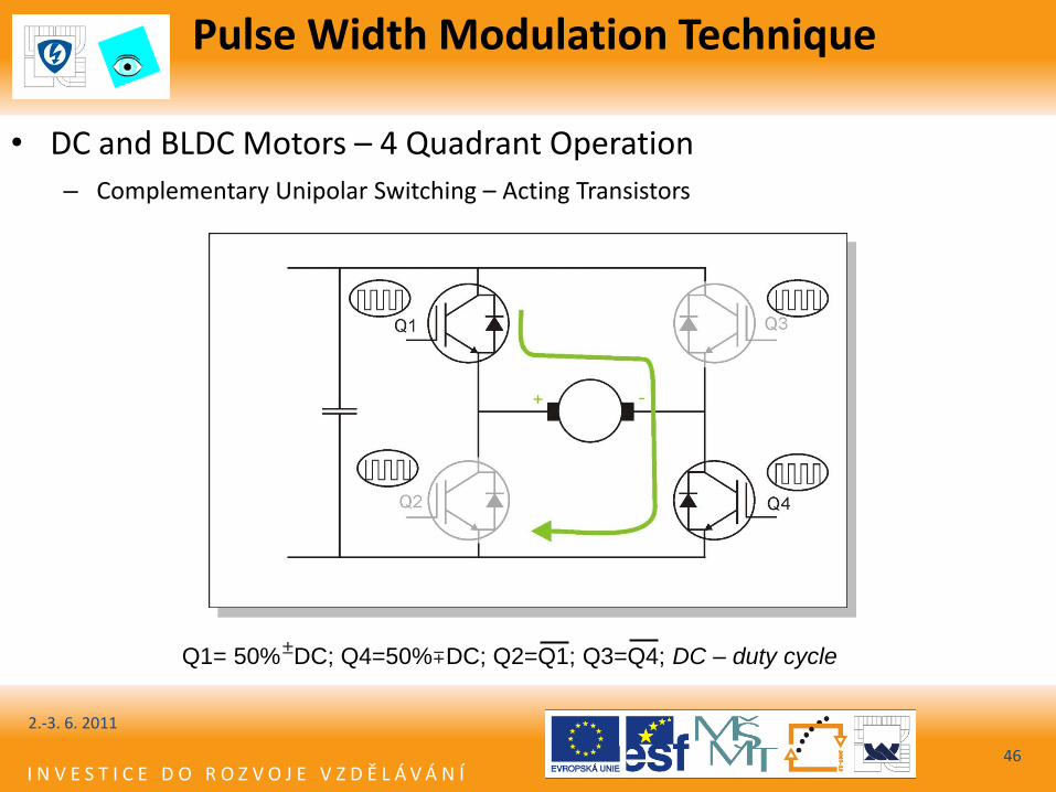
• DC and BLDC Motors – 4 Quadrant Operation
– Complementary Unipolar Switching – Acting Transistors
Q1= 50% DC; Q4=50% DC; Q2=Q1; Q3=Q4; DC – duty cycle ± ±
2.-3. 6. 2011
I N V E S T I C E D O R O Z V O J E V Z D Ě L Á V Á N Í
Pulse Width Modulation Technique
47
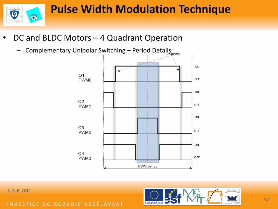
• DC and BLDC Motors – 4 Quadrant Operation
– Complementary Unipolar Switching – Period Details
2.-3. 6. 2011
I N V E S T I C E D O R O Z V O J E V Z D Ě L Á V Á N Í
Pulse Width Modulation Technique
48
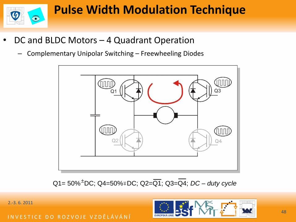
• DC and BLDC Motors – 4 Quadrant Operation
– Complementary Unipolar Switching – Freewheeling Diodes
Q1= 50% DC; Q4=50% DC; Q2=Q1; Q3=Q4; DC – duty cycle ± ±
2.-3. 6. 2011
I N V E S T I C E D O R O Z V O J E V Z D Ě L Á V Á N Í
Pulse Width Modulation Technique
49
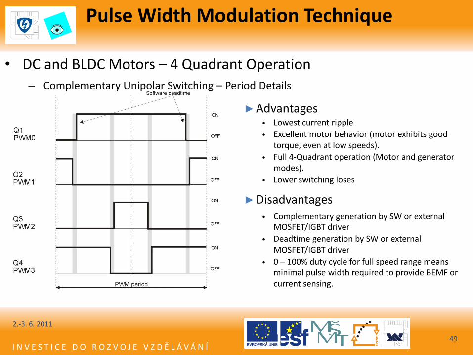
• DC and BLDC Motors – 4 Quadrant Operation
– Complementary Unipolar Switching – Period Details
►Advantages
• Lowest current ripple
• Excellent motor behavior (motor exhibits good torque, even at low speeds).
• Full 4-Quadrant operation (Motor and generator modes).
• Lower switching loses
►Disadvantages • Complementary generation by SW or external
MOSFET/IGBT driver
• Deadtime generation by SW or external MOSFET/IGBT driver
• 0 – 100% duty cycle for full speed range means minimal pulse width required to provide BEMF or current sensing.
2.-3. 6. 2011
I N V E S T I C E D O R O Z V O J E V Z D Ě L Á V Á N Í
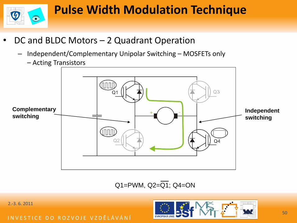
Pulse Width Modulation Technique
50
• DC and BLDC Motors – 2 Quadrant Operation
– Independent/Complementary Unipolar Switching – MOSFETs only – Acting Transistors
Q1=PWM, Q2=Q1; Q4=ON
Complementary
switching Independent
switching
2.-3. 6. 2011
I N V E S T I C E D O R O Z V O J E V Z D Ě L Á V Á N Í
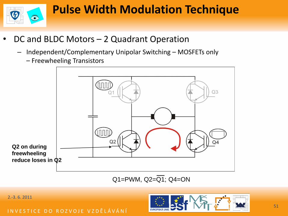
Pulse Width Modulation Technique
51
• DC and BLDC Motors – 2 Quadrant Operation
– Independent/Complementary Unipolar Switching – MOSFETs only – Freewheeling Transistors
Q1=PWM, Q2=Q1; Q4=ON
Q2 on during
freewheeling
reduce loses in Q2
2.-3. 6. 2011
I N V E S T I C E D O R O Z V O J E V Z D Ě L Á V Á N Í
Pulse Width Modulation Technique - Summary
• 1/2/4 Quadrant Operation
– Single Quadrant Operation • Single direction of rotation (DC motors only)
– Two Quadrant Operation
• Both direction of rotation
• Can not work as generator (brake)
– Four Quadrant Operation
• Both direction of rotation
• Can work as motor and generator as well
52
2.-3. 6. 2011
I N V E S T I C E D O R O Z V O J E V Z D Ě L Á V Á N Í
Pulse Width Modulation Technique - Summary
• Independent/Complementary switching
– Independent
• 2 quadrant operation only
• do not need complementary and dead-time logic
– Complementary
• 4 quadrant operation
• Unipolar/Bipolar switching
– Unipolar – lower loses, preferred
– Bipolar – higher loses against to unipolar
• Edge/Center Aligned switching
– Doesn't make sense for DC and BLDC motor
– Center Aligned PWM reduce EMI noise
53
2.-3. 6. 2011

I N V E S T I C E D O R O Z V O J E V Z D Ě L Á V Á N Í
Pulse Width Modulation Technique - Summary
• PWM Techniques – Independent Bipolar PWM
• Not recommended due to discontinuous current
– Complementary Bipolar PWM
• Use for 4 quadrant drives
– Independent Unipolar PWM
• Best choice for 2 quadrant drives
– Complementary Unipolar PWM
• Best choice for 4 quadrant drives
– Independent/Complementary Unipolar PWM
• Best choice for MOSFET H-bridge and 2 quadrant drive
54
2.-3. 6. 2011
I N V E S T I C E D O R O Z V O J E V Z D Ě L Á V Á N Í
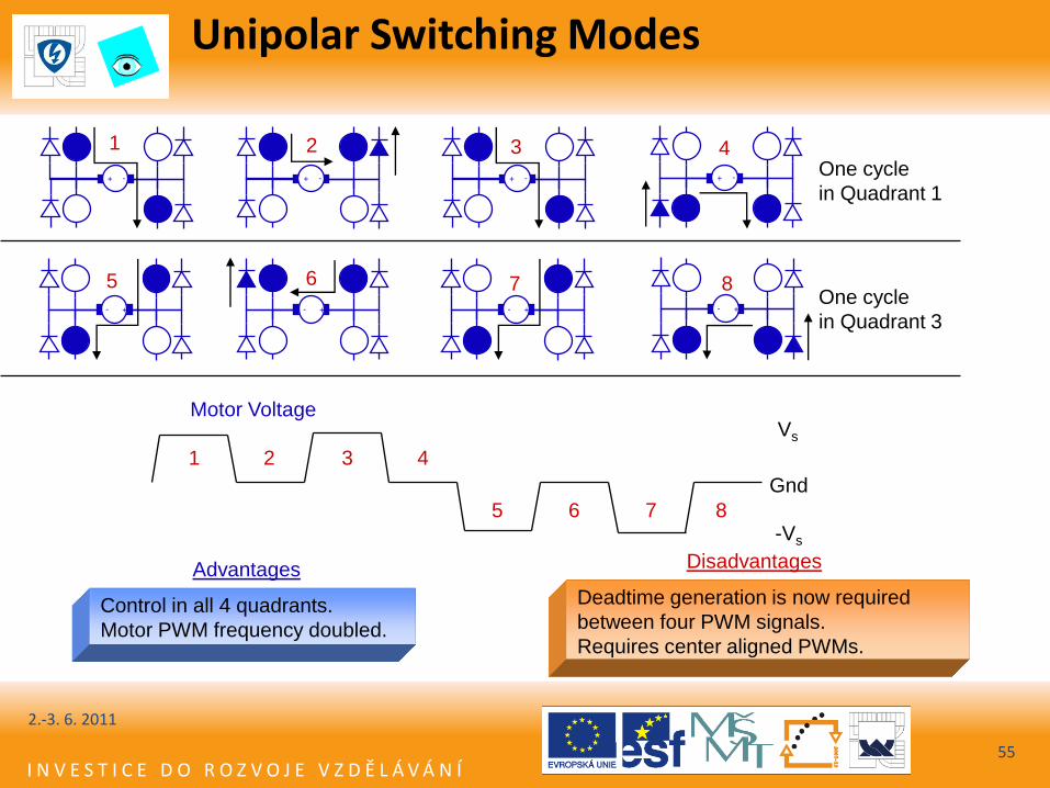
Advantages
Deadtime generation is now required
between four PWM signals.
Requires center aligned PWMs.
Disadvantages
Control in all 4 quadrants.
Motor PWM frequency doubled.
-Vs
Vs Motor Voltage
- + - + - + - + One cycle
in Quadrant 1
One cycle
in Quadrant 3 - + - + - + - +
1 2 3 4
5 6 7 8
2 3 4
5 6 7 8
1
Gnd
Unipolar Switching Modes
2.-3. 6. 2011
55
I N V E S T I C E D O R O Z V O J E V Z D Ě L Á V Á N Í
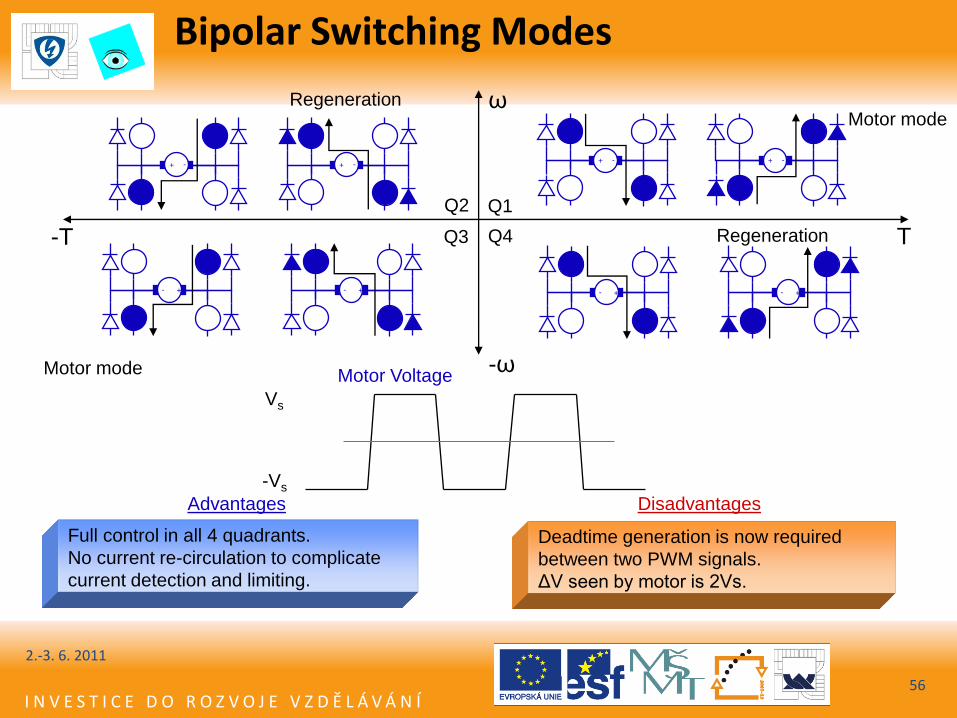
Q1 Q2
Q3 Q4
- + - + - + - +
Regeneration
Regeneration ω
-ω
T -T
- + - + - + - +
Advantages
Deadtime generation is now required
between two PWM signals.
ΔV seen by motor is 2Vs.
Disadvantages
Full control in all 4 quadrants.
No current re-circulation to complicate
current detection and limiting.
-Vs
Vs
Motor Voltage
Bipolar Switching Modes
Motor mode
Motor mode
2.-3. 6. 2011
56
I N V E S T I C E D O R O Z V O J E V Z D Ě L Á V Á N Í
Agenda
• Separately exited DC motor
• Basic Terms
• PWM Modulation techniques for DC and BLDC drives
• BLDC Motor Theory
– Brush DC Motor Principle
– BLDC Motor Principle
– Basic Control Techniques
– BLDC versus PMSM motor
• Microcontroller MC56F8006
57
2.-3. 6. 2011
I N V E S T I C E D O R O Z V O J E V Z D Ě L Á V Á N Í
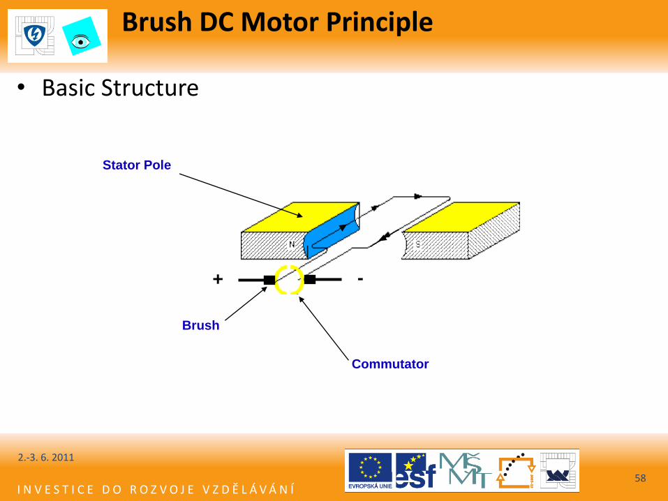
Brush DC Motor Principle
• Basic Structure
+ -
Stator Pole
Commutator
Brush
58
2.-3. 6. 2011
I N V E S T I C E D O R O Z V O J E V Z D Ě L Á V Á N Í
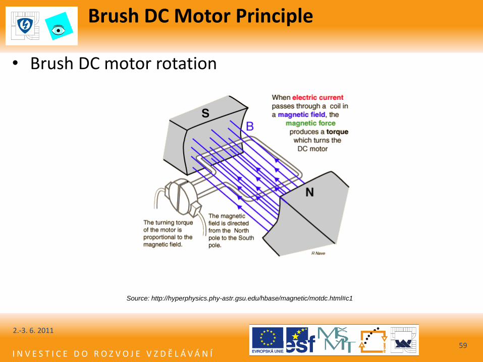
Brush DC Motor Principle
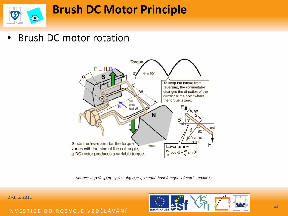
• Brush DC motor rotation
Source: http://hyperphysics.phy-astr.gsu.edu/hbase/magnetic/motdc.html#c1
59
2.-3. 6. 2011
I N V E S T I C E D O R O Z V O J E V Z D Ě L Á V Á N Í
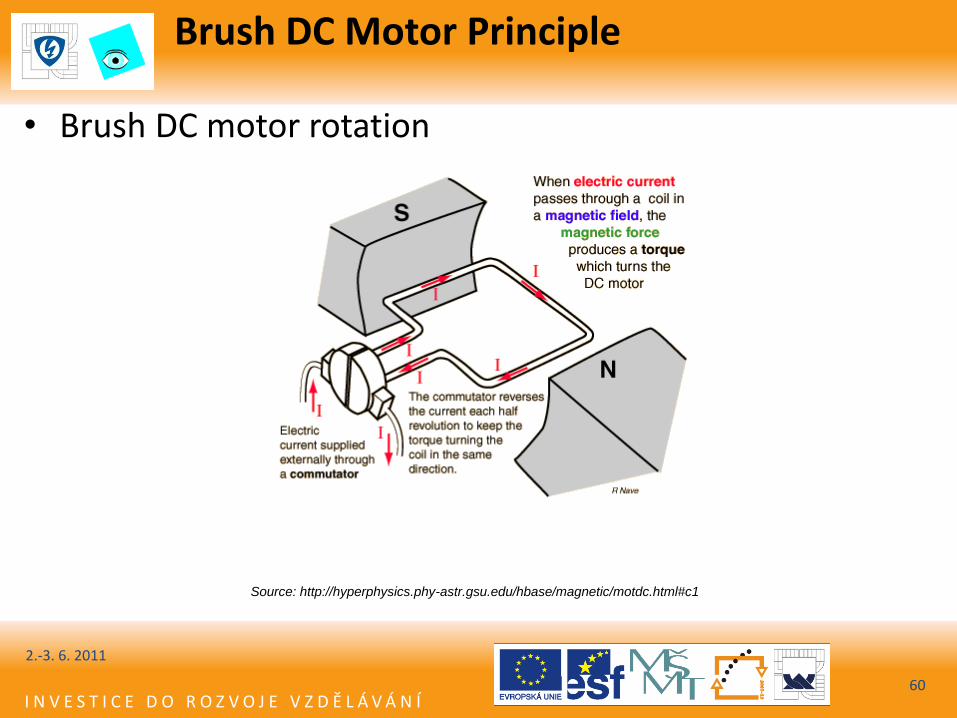
Brush DC Motor Principle
• Brush DC motor rotation
Source: http://hyperphysics.phy-astr.gsu.edu/hbase/magnetic/motdc.html#c1
60
2.-3. 6. 2011
I N V E S T I C E D O R O Z V O J E V Z D Ě L Á V Á N Í
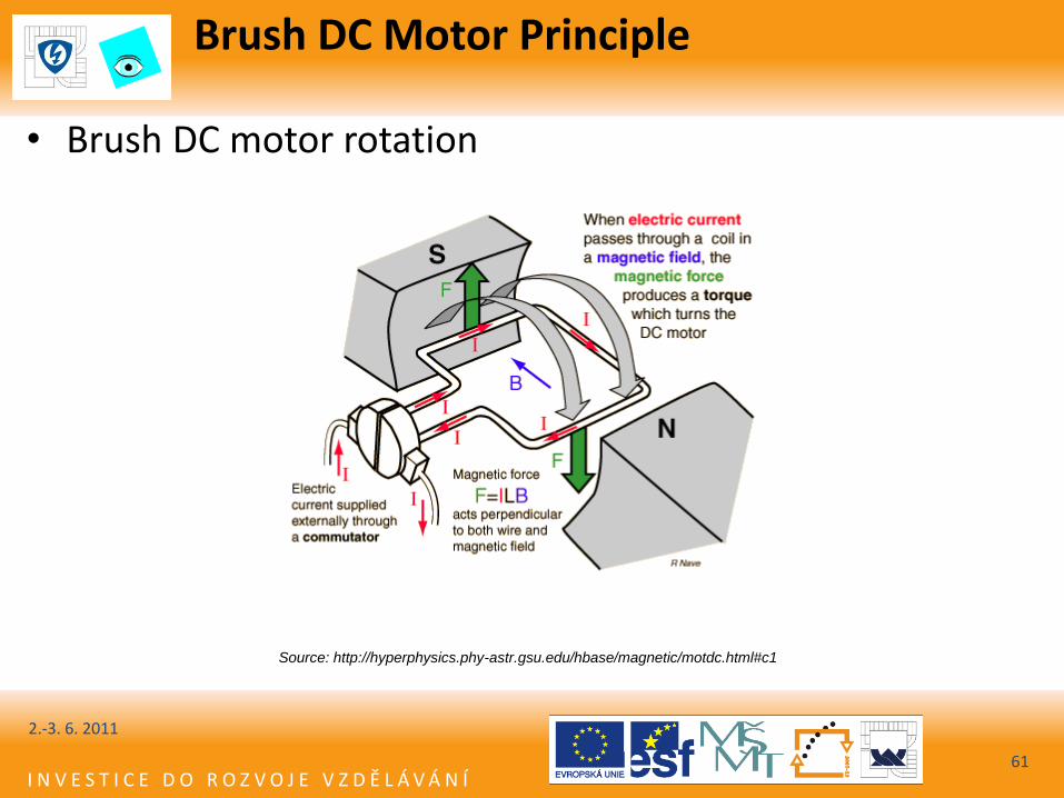
Brush DC Motor Principle
• Brush DC motor rotation
Source: http://hyperphysics.phy-astr.gsu.edu/hbase/magnetic/motdc.html#c1
61
2.-3. 6. 2011
I N V E S T I C E D O R O Z V O J E V Z D Ě L Á V Á N Í
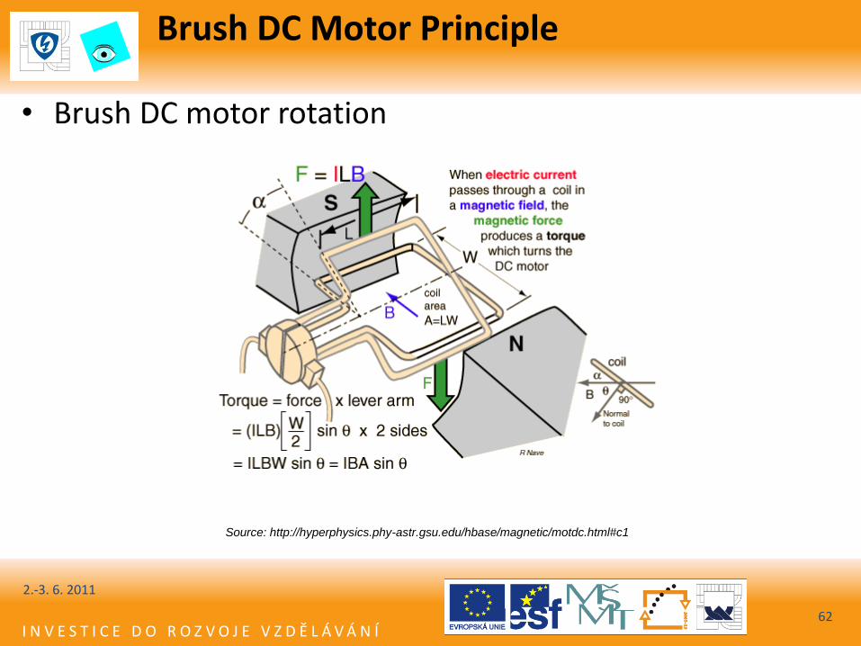
Brush DC Motor Principle
• Brush DC motor rotation
Source: http://hyperphysics.phy-astr.gsu.edu/hbase/magnetic/motdc.html#c1
62
2.-3. 6. 2011
I N V E S T I C E D O R O Z V O J E V Z D Ě L Á V Á N Í
Brush DC Motor Principle
• Brush DC motor rotation
Source: http://hyperphysics.phy-astr.gsu.edu/hbase/magnetic/motdc.html#c1
63
2.-3. 6. 2011
I N V E S T I C E D O R O Z V O J E V Z D Ě L Á V Á N Í
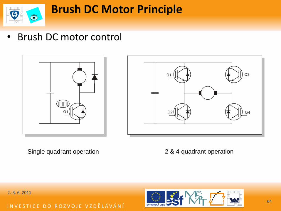
Brush DC Motor Principle
• Brush DC motor control
Single quadrant operation 2 & 4 quadrant operation
64
2.-3. 6. 2011
I N V E S T I C E D O R O Z V O J E V Z D Ě L Á V Á N Í
Brush DC Motor Principle
• Advantages – Ease of control (self commutating).
– Low rotor inertia (coreless rotors).
– Lowest total system cost for basic motion.
– Wound field motors exhibit high starting torque, (series wound) and can run with AC or DC.
• Disadvantages
– Higher maintenance cost due to brush wear.
– Electrical noise due to mechanical commutation.
– Maximal speed limited by commutator
– Heat is generated in armature, which is difficult to remove.
– Friction losses associated with mechanical commutation.
– Not usable in “intrinsically safe” environments.
65
2.-3. 6. 2011
I N V E S T I C E D O R O Z V O J E V Z D Ě L Á V Á N Í
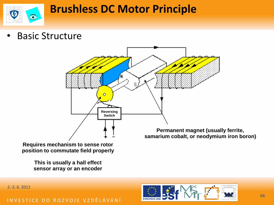
Brushless DC Motor Principle
• Basic Structure
Requires mechanism to sense rotor position to commutate field properly
This is usually a hall effect sensor array or an encoder
Reversing Switch
Permanent magnet (usually ferrite, samarium cobalt, or neodymium iron boron)
66
2.-3. 6. 2011
I N V E S T I C E D O R O Z V O J E V Z D Ě L Á V Á N Í
Brushless DC Motor Principle
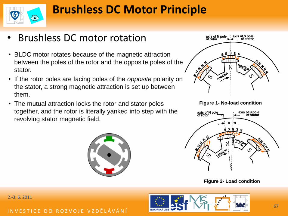
• Brushless DC motor rotation
• BLDC motor rotates because of the magnetic attraction
between the poles of the rotor and the opposite poles of the
stator.
• If the rotor poles are facing poles of the opposite polarity on
the stator, a strong magnetic attraction is set up between
them.
• The mutual attraction locks the rotor and stator poles
together, and the rotor is literally yanked into step with the
revolving stator magnetic field.
axis of N pole of rotor
axis of S pole of stator
S S S S S
NN
NN
N
N
NN
NN
rotation N
S
S rota
tion
axis of N pole of rotor
axis of S pole of stator
S S S S S
NN
NN
N
NN
NN
N
N
NN
NN
N
NN
NN
rotation N
S
S rota
tion
rota
tion
axis of N pole of rotor
axis of S pole of stator
S S S S S
N
NN
NN
N
NN
NN
NS
S
rotation
rota
tion
axis of N pole of rotor
axis of S pole of stator
S S S S S
N
NN
NN
N
NN
NN
NS
S
rotation
rota
tion
Figure 1- No-load condition
Figure 2- Load condition
67
2.-3. 6. 2011
I N V E S T I C E D O R O Z V O J E V Z D Ě L Á V Á N Í
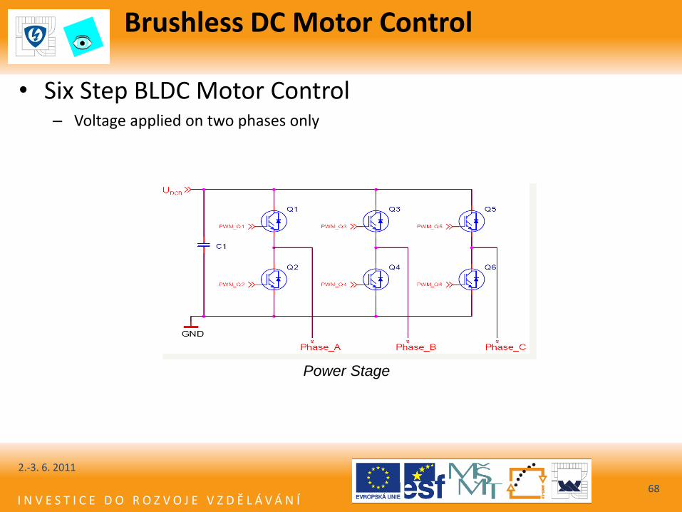
Brushless DC Motor Control
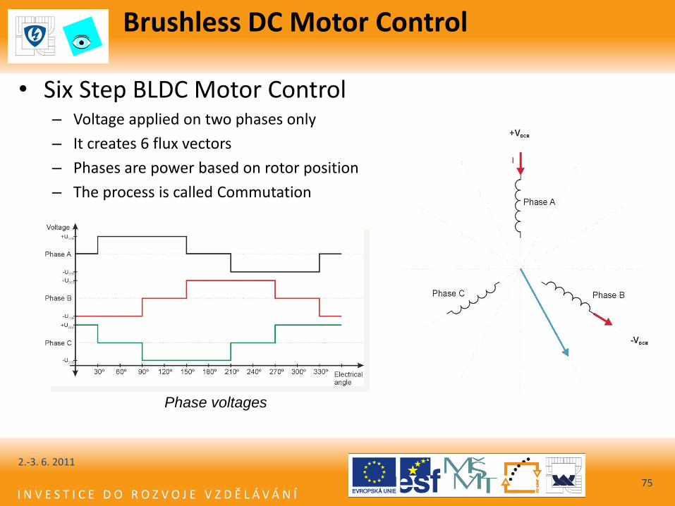
• Six Step BLDC Motor Control – Voltage applied on two phases only
Power Stage
68
2.-3. 6. 2011
I N V E S T I C E D O R O Z V O J E V Z D Ě L Á V Á N Í
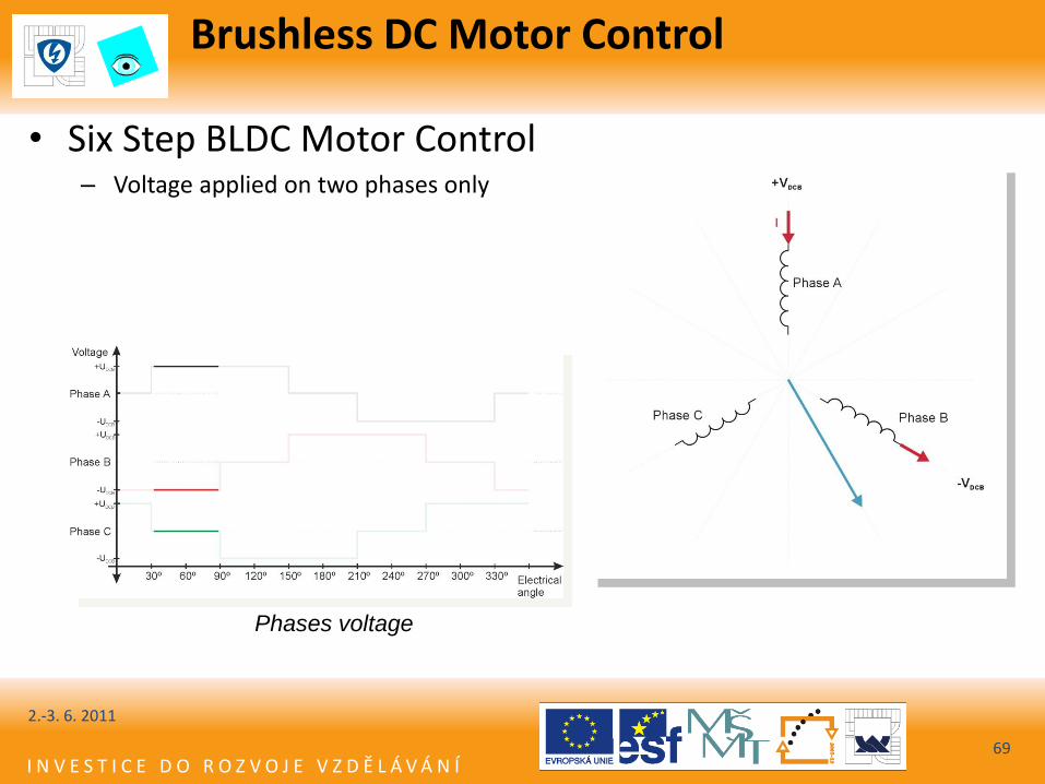
Brushless DC Motor Control
• Six Step BLDC Motor Control – Voltage applied on two phases only
Phases voltage
69
2.-3. 6. 2011

I N V E S T I C E D O R O Z V O J E V Z D Ě L Á V Á N Í
Brushless DC Motor Control
• Six Step BLDC Motor Control – Voltage applied on two phases only
Phases voltage
70
2.-3. 6. 2011

I N V E S T I C E D O R O Z V O J E V Z D Ě L Á V Á N Í
Brushless DC Motor Control
• Six Step BLDC Motor Control – Voltage applied on two phases only
Phases voltage
71
2.-3. 6. 2011
I N V E S T I C E D O R O Z V O J E V Z D Ě L Á V Á N Í
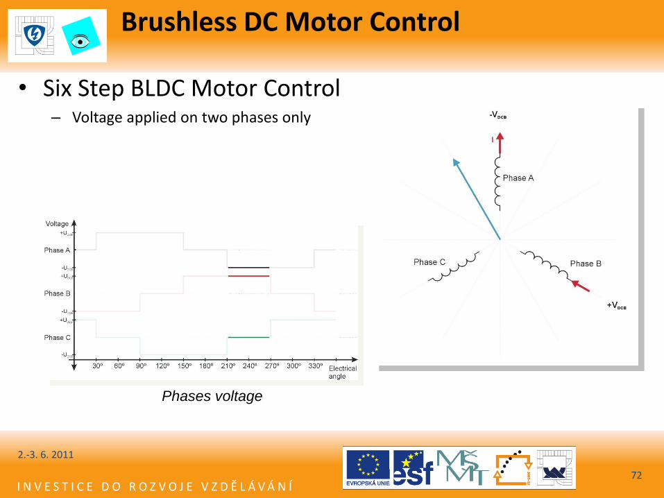
Brushless DC Motor Control
• Six Step BLDC Motor Control – Voltage applied on two phases only
Phases voltage
72
2.-3. 6. 2011

I N V E S T I C E D O R O Z V O J E V Z D Ě L Á V Á N Í
Brushless DC Motor Control
• Six Step BLDC Motor Control – Voltage applied on two phases only
Phases voltage
73
2.-3. 6. 2011

I N V E S T I C E D O R O Z V O J E V Z D Ě L Á V Á N Í
Brushless DC Motor Control
• Six Step BLDC Motor Control – Voltage applied on two phases only
Phases voltage
74
2.-3. 6. 2011
I N V E S T I C E D O R O Z V O J E V Z D Ě L Á V Á N Í
Brushless DC Motor Control
• Six Step BLDC Motor Control – Voltage applied on two phases only
– It creates 6 flux vectors
– Phases are power based on rotor position
– The process is called Commutation
Phase voltages
2.-3. 6. 2011
75
I N V E S T I C E D O R O Z V O J E V Z D Ě L Á V Á N Í
S N
N
S
N
S
S N N
S S
N
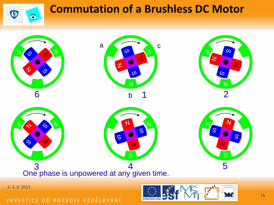
One phase is unpowered at any given time.
2
3 4 5
6
a c
b 1
Commutation of a Brushless DC Motor
2.-3. 6. 2011
76
I N V E S T I C E D O R O Z V O J E V Z D Ě L Á V Á N Í
Brushless DC Motor Control
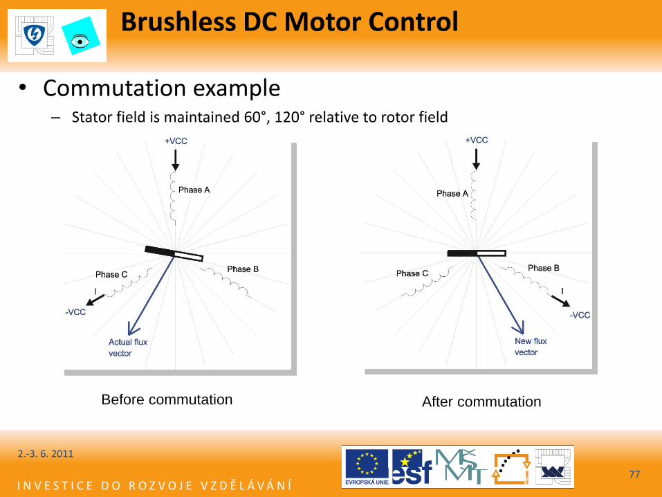
• Commutation example – Stator field is maintained 60°, 120° relative to rotor field
Before commutation After commutation
2.-3. 6. 2011
77
I N V E S T I C E D O R O Z V O J E V Z D Ě L Á V Á N Í
Brushless DC Motor Control
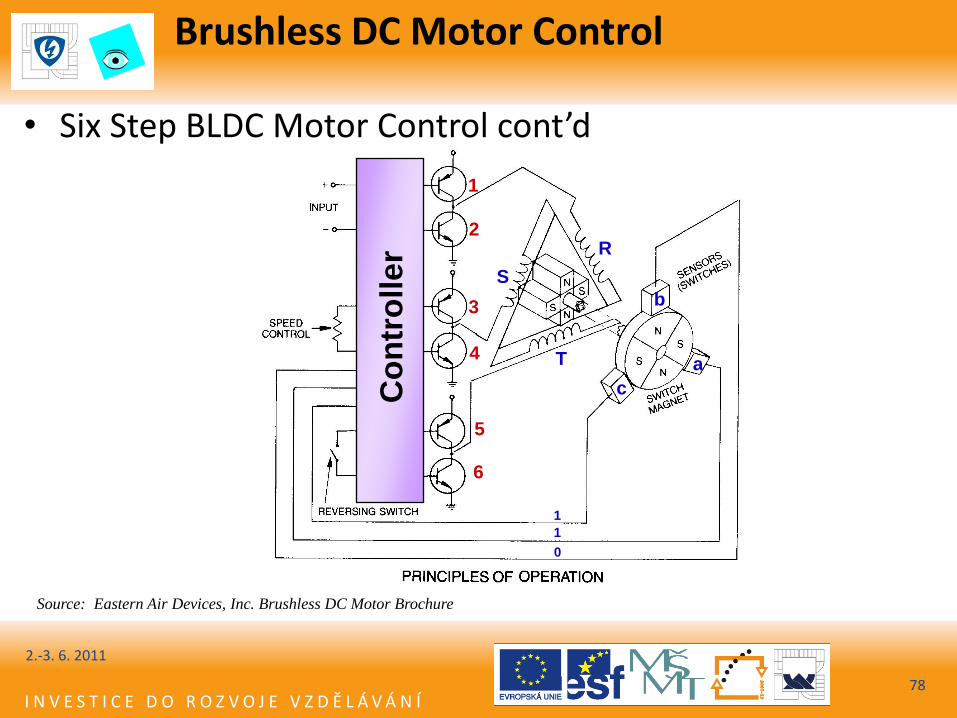
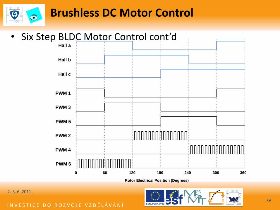
• Six Step BLDC Motor Control cont’d
1
2
3
4
5
6
S
R
T
b
a
c Co
ntr
oller
Source: Eastern Air Devices, Inc. Brushless DC Motor Brochure
1
1
0
2.-3. 6. 2011
78
I N V E S T I C E D O R O Z V O J E V Z D Ě L Á V Á N Í
Brushless DC Motor Control
• Six Step BLDC Motor Control cont’d
PWM 1
PWM 3
PWM 5
PWM 2
PWM 4
PWM 6
Hall a
Hall b
Hall c
0 60 120 180 240 300 360
Rotor Electrical Position (Degrees)
2.-3. 6. 2011
79
I N V E S T I C E D O R O Z V O J E V Z D Ě L Á V Á N Í
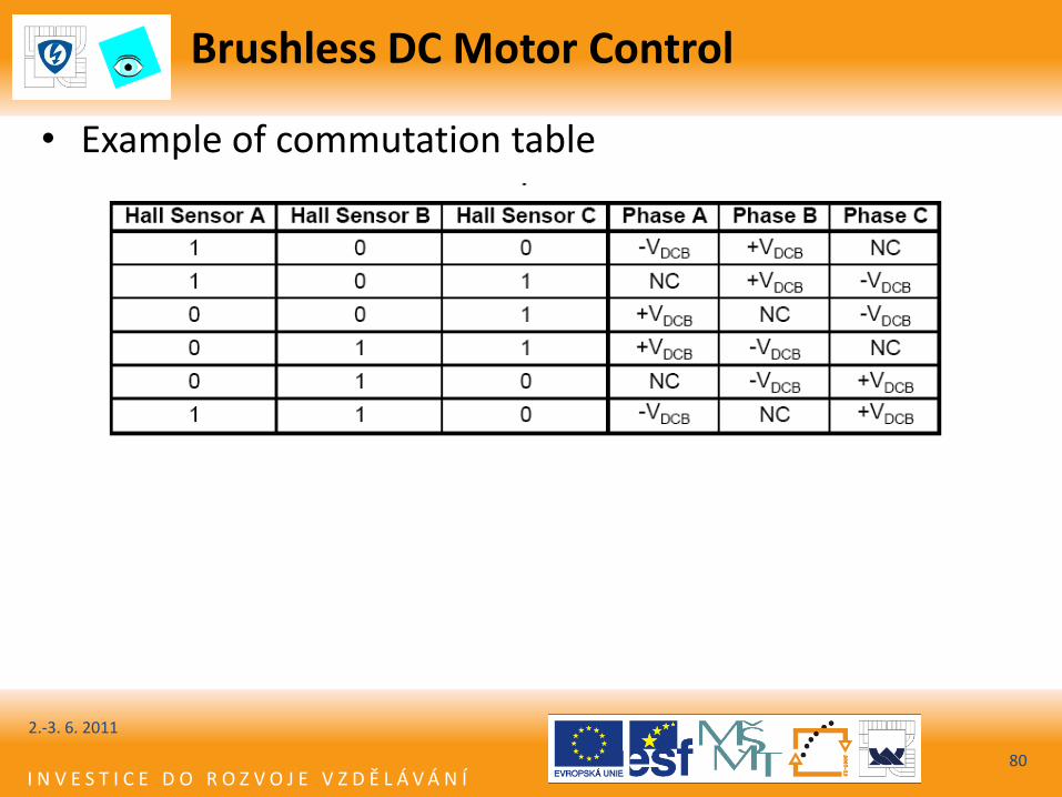
Brushless DC Motor Control
• Example of commutation table
2.-3. 6. 2011
80
I N V E S T I C E D O R O Z V O J E V Z D Ě L Á V Á N Í
Brushless DC Motor Control
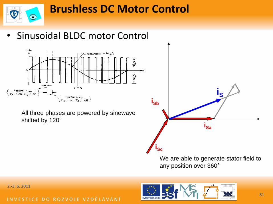
• Sinusoidal BLDC motor Control
iS
iSa
iSb
iSc
All three phases are powered by sinewave
shifted by 120°
We are able to generate stator field to
any position over 360°
2.-3. 6. 2011
81
I N V E S T I C E D O R O Z V O J E V Z D Ě L Á V Á N Í
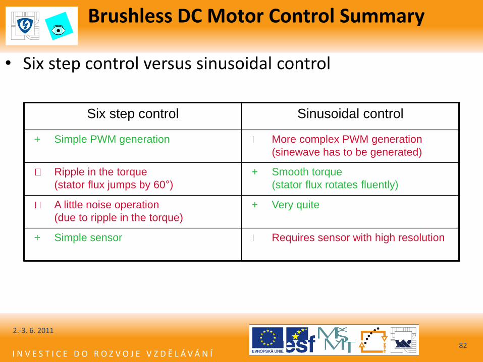
Brushless DC Motor Control Summary
Six step control Sinusoidal control
+ Simple PWM generation More complex PWM generation
(sinewave has to be generated)
Ripple in the torque
(stator flux jumps by 60°)
+ Smooth torque
(stator flux rotates fluently)
A little noise operation
(due to ripple in the torque)
+ Very quite
+ Simple sensor Requires sensor with high resolution
82
• Six step control versus sinusoidal control
2.-3. 6. 2011
I N V E S T I C E D O R O Z V O J E V Z D Ě L Á V Á N Í
Brushless DC Motor Control
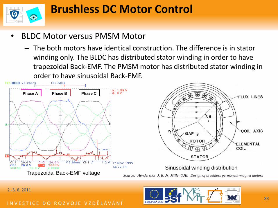
• BLDC Motor versus PMSM Motor – The both motors have identical construction. The difference is in stator
winding only. The BLDC has distributed stator winding in order to have trapezoidal Back-EMF. The PMSM motor has distributed stator winding in order to have sinusoidal Back-EMF.
Phase A Phase B Phase C
Trapezoidal Back-EMF voltage Sinusoidal winding distribution
Source: Hendershot J. R. Jr, Miller TJE: Design of brushless permanent-magnet motors
2.-3. 6. 2011
83
I N V E S T I C E D O R O Z V O J E V Z D Ě L Á V Á N Í
Commutation Table
• The commutation table is fundamental for six step commutation BLDC control algorithm
• Motor commutates and thus rotates according to the commutation table
• The commutation table must be created depending on the actual motor configuration
2.-3. 6. 2011
84
I N V E S T I C E D O R O Z V O J E V Z D Ě L Á V Á N Í
Commutation Table
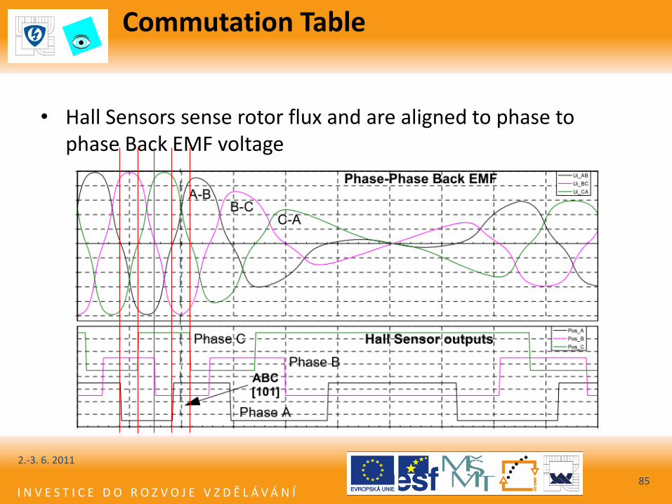
• Hall Sensors sense rotor flux and are aligned to phase to phase Back EMF voltage
2.-3. 6. 2011
85
I N V E S T I C E D O R O Z V O J E V Z D Ě L Á V Á N Í
How to Get Commutation Table?
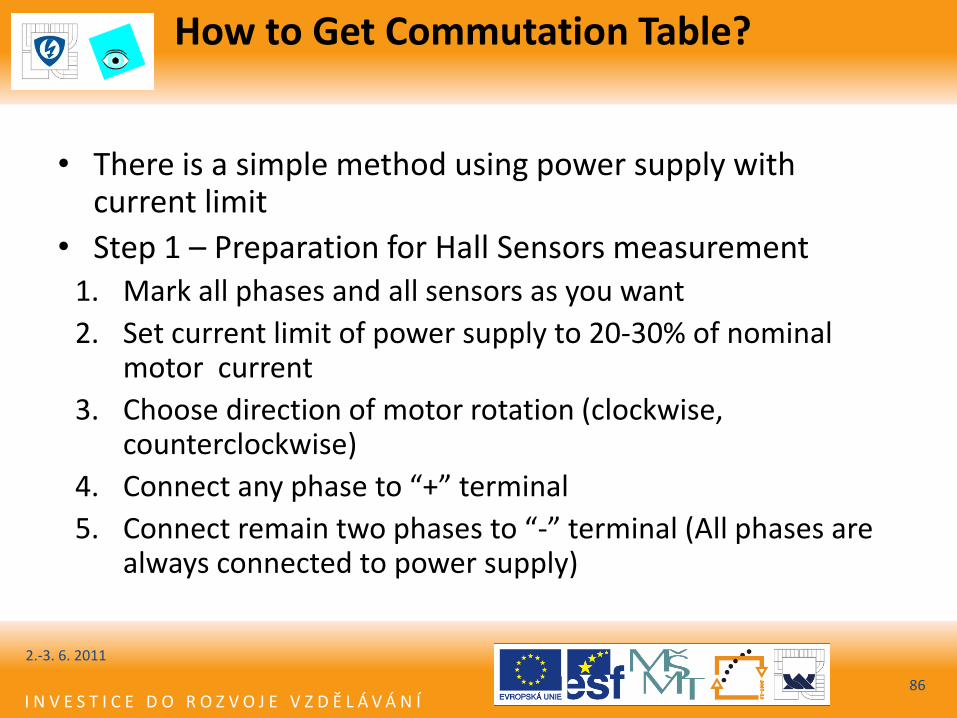
• There is a simple method using power supply with current limit
• Step 1 – Preparation for Hall Sensors measurement 1. Mark all phases and all sensors as you want
2. Set current limit of power supply to 20-30% of nominal motor current
3. Choose direction of motor rotation (clockwise, counterclockwise)
4. Connect any phase to “+” terminal
5. Connect remain two phases to “-” terminal (All phases are always connected to power supply)
2.-3. 6. 2011
86

I N V E S T I C E D O R O Z V O J E V Z D Ě L Á V Á N Í
How to Get Commutation Table?
• Step 2 – Hall Sensors Measurement
Phase Hall Sensor
A B C a b c
+ - - 1 1 0
2.-3. 6. 2011
87
I N V E S T I C E D O R O Z V O J E V Z D Ě L Á V Á N Í
How to Get Commutation Table?
• Step 2 - Hall Sensors Measurement
Phase Hall Sensor
A B C a b c
+ - - 1 1 0
+ + - 0 1 0
2.-3. 6. 2011
88

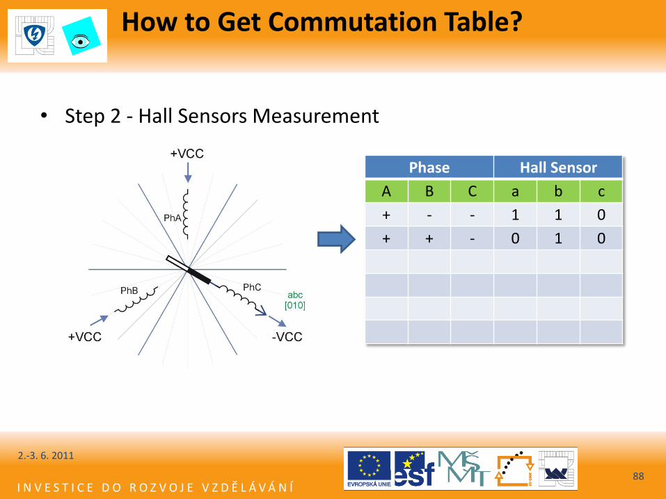
I N V E S T I C E D O R O Z V O J E V Z D Ě L Á V Á N Í
How to Get Commutation Table?
• Step 2 - Hall Sensors Measurement
Phase Hall Sensor
A B C a b c
+ - - 1 1 0
+ + - 0 1 0
- + - 0 1 1
2.-3. 6. 2011
89
I N V E S T I C E D O R O Z V O J E V Z D Ě L Á V Á N Í
How to Get Commutation Table?
• Step 2 - Hall Sensors Measurement
Phase Hall Sensor
A B C a b c
+ - - 1 1 0
+ + - 0 1 0
- + - 0 1 1
- + + 0 0 1
2.-3. 6. 2011
90
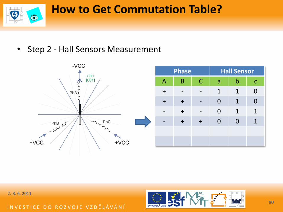
I N V E S T I C E D O R O Z V O J E V Z D Ě L Á V Á N Í
How to Get Commutation Table?
• Step 2 - Hall Sensors Measurement
Phase Hall Sensor
A B C a b c
+ - - 1 1 0
+ + - 0 1 0
- + - 0 1 1
- + + 0 0 1
- - + 1 0 1
2.-3. 6. 2011
91
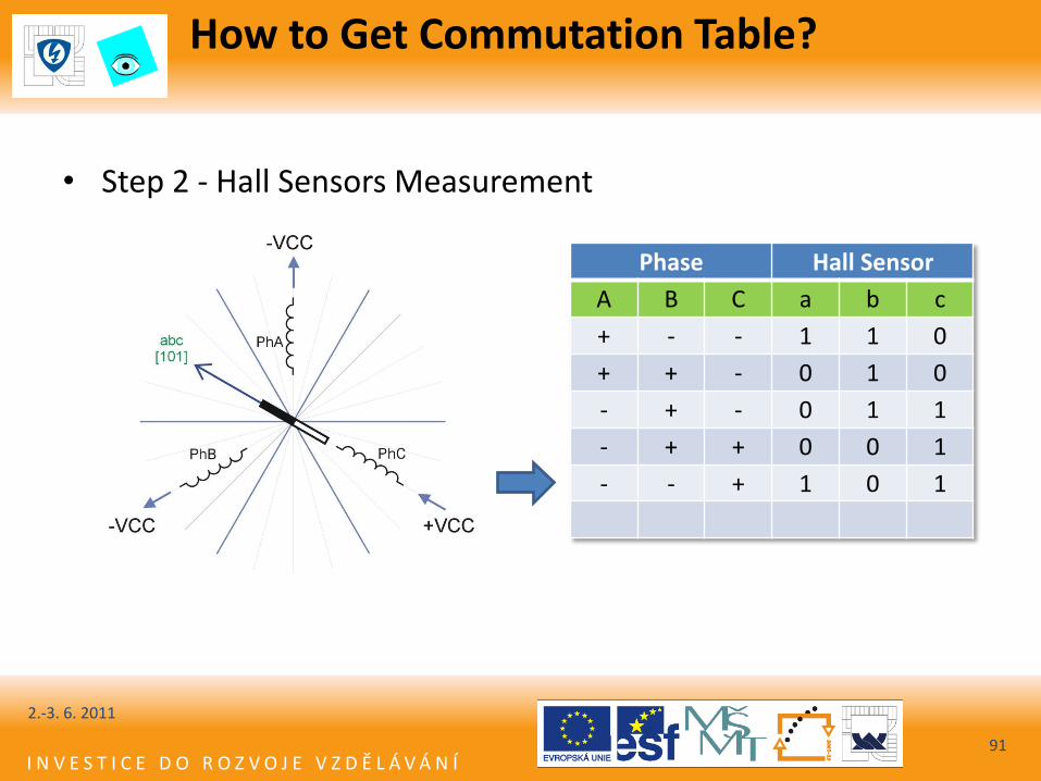
I N V E S T I C E D O R O Z V O J E V Z D Ě L Á V Á N Í
How to Get Commutation Table?
• Step 2 - Hall Sensors Measurement
Phase Hall Sensor
A B C a b c
+ - - 1 1 0
+ + - 0 1 0
- + - 0 1 1
- + + 0 0 1
- - + 1 0 1
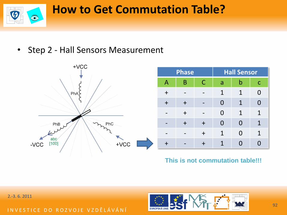
+ - + 1 0 0
This is not commutation table!!!
2.-3. 6. 2011
92

I N V E S T I C E D O R O Z V O J E V Z D Ě L Á V Á N Í
How to Get Commutation Table?
• Step 3 - Making Commutation Table
Hall Sensors Phase
a b c A B C
1 1 0 NC + -
0 1 0
0 1 1
0 0 1
1 0 1
1 0 0
2.-3. 6. 2011
93
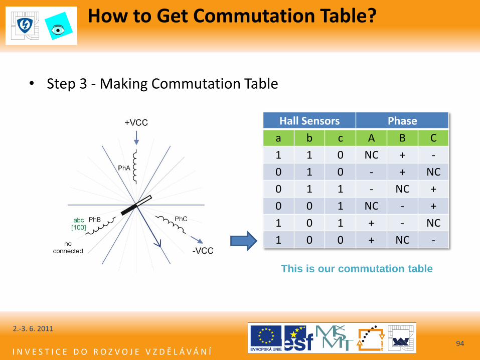
I N V E S T I C E D O R O Z V O J E V Z D Ě L Á V Á N Í
How to Get Commutation Table?
• Step 3 - Making Commutation Table
Hall Sensors Phase
a b c A B C
1 1 0 NC + -
0 1 0 - + NC
0 1 1 - NC +
0 0 1 NC - +
1 0 1 + - NC
1 0 0 + NC -
This is our commutation table
2.-3. 6. 2011
94
I N V E S T I C E D O R O Z V O J E V Z D Ě L Á V Á N Í
Agenda
• Separately exited DC motor
• Basic Terms
• PWM Modulation techniques for DC and BLDC drives
• BLDC Motor Theory
• Microcontroller MC56F8006
– Microcontroller roadmap
– Microcontroller overview
– Peripherals
2.-3. 6. 2011
95

I N V E S T I C E D O R O Z V O J E V Z D Ě L Á V Á N Í
DSCS - 56F8006/2
2.-3. 6. 2011
96
I N V E S T I C E D O R O Z V O J E V Z D Ě L Á V Á N Í
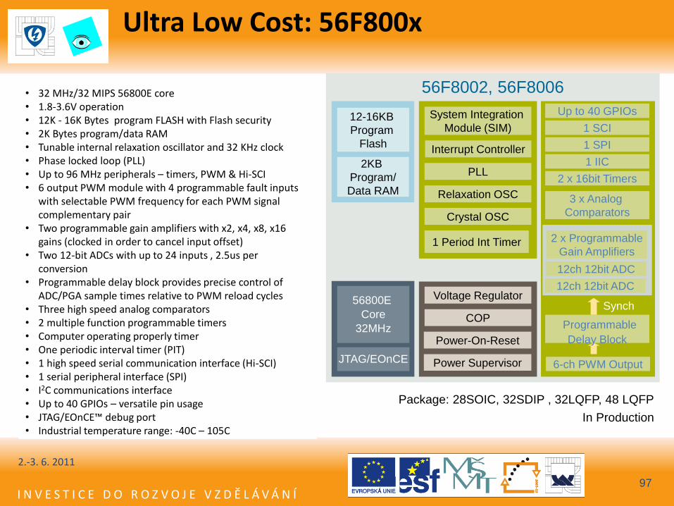
Ultra Low Cost: 56F800x
• 32 MHz/32 MIPS 56800E core • 1.8-3.6V operation • 12K - 16K Bytes program FLASH with Flash security • 2K Bytes program/data RAM • Tunable internal relaxation oscillator and 32 KHz clock • Phase locked loop (PLL) • Up to 96 MHz peripherals – timers, PWM & Hi-SCI • 6 output PWM module with 4 programmable fault inputs
with selectable PWM frequency for each PWM signal complementary pair
• Two programmable gain amplifiers with x2, x4, x8, x16 gains (clocked in order to cancel input offset)
• Two 12-bit ADCs with up to 24 inputs , 2.5us per conversion
• Programmable delay block provides precise control of ADC/PGA sample times relative to PWM reload cycles
• Three high speed analog comparators • 2 multiple function programmable timers • Computer operating properly timer • One periodic interval timer (PIT) • 1 high speed serial communication interface (Hi-SCI) • 1 serial peripheral interface (SPI) • I2C communications interface • Up to 40 GPIOs – versatile pin usage • JTAG/EOnCE™ debug port • Industrial temperature range: -40C – 105C
97
56800E
Core
32MHz Power-On-Reset
Power Supervisor
COP
12-16KB
Program
Flash
6-ch PWM Output
System Integration
Module (SIM) 1 SCI
1 SPI
1 IIC
JTAG/EOnCE
2KB
Program/
Data RAM
Voltage Regulator
PLL
Interrupt Controller
Relaxation OSC
2 x Programmable
Gain Amplifiers
56F8002, 56F8006
Up to 40 GPIOs
Programmable
Delay Block
Synch
2 x 16bit Timers
Crystal OSC
3 x Analog
Comparators
1 Period Int Timer
12ch 12bit ADC
12ch 12bit ADC
Package: 28SOIC, 32SDIP , 32LQFP, 48 LQFP
In Production
2.-3. 6. 2011
I N V E S T I C E D O R O Z V O J E V Z D Ě L Á V Á N Í
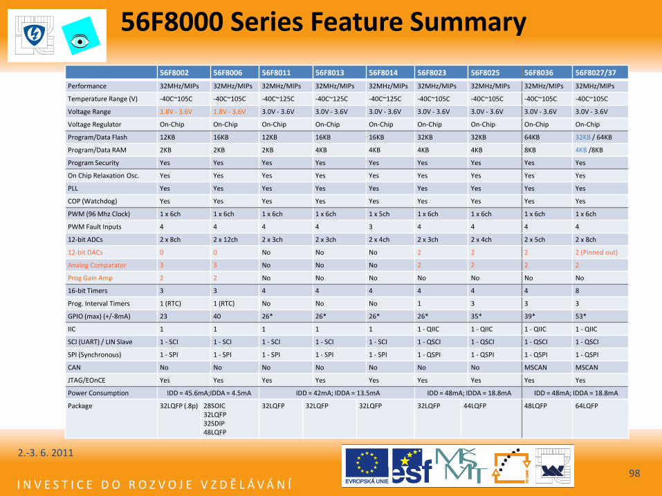
56F8000 Series Feature Summary
56F8002 56F8006 56F8011 56F8013 56F8014 56F8023 56F8025 56F8036 56F8027/37
Performance 32MHz/MIPs 32MHz/MIPs 32MHz/MIPs 32MHz/MIPs 32MHz/MIPs 32MHz/MIPs 32MHz/MIPs 32MHz/MIPs 32MHz/MIPs
Temperature Range (V) -40C~105C -40C~105C -40C~125C -40C~125C -40C~125C -40C~105C -40C~105C -40C~105C -40C~105C
Voltage Range 1.8V - 3.6V 1.8V - 3.6V 3.0V - 3.6V 3.0V - 3.6V 3.0V - 3.6V 3.0V - 3.6V 3.0V - 3.6V 3.0V - 3.6V 3.0V - 3.6V
Voltage Regulator On-Chip On-Chip On-Chip On-Chip On-Chip On-Chip On-Chip On-Chip On-Chip
Program/Data Flash 12KB 16KB 12KB 16KB 16KB 32KB 32KB 64KB 32KB / 64KB
Program/Data RAM 2KB 2KB 2KB 4KB 4KB 4KB 4KB 8KB 4KB /8KB
Program Security Yes Yes Yes Yes Yes Yes Yes Yes Yes
On Chip Relaxation Osc. Yes Yes Yes Yes Yes Yes Yes Yes Yes
PLL Yes Yes Yes Yes Yes Yes Yes Yes Yes
COP (Watchdog) Yes Yes Yes Yes Yes Yes Yes Yes Yes
PWM (96 Mhz Clock) 1 x 6ch 1 x 6ch 1 x 6ch 1 x 6ch 1 x 5ch 1 x 6ch 1 x 6ch 1 x 6ch 1 x 6ch
PWM Fault Inputs 4 4 4 4 3 4 4 4 4
12-bit ADCs 2 x 8ch 2 x 12ch 2 x 3ch 2 x 3ch 2 x 4ch 2 x 3ch 2 x 4ch 2 x 5ch 2 x 8ch
12-bit DACs 0 0 No No No 2 2 2 2 (Pinned out)
Analog Comparator 3 3 No No No 2 2 2 2
Prog Gain Amp 2 2 No No No No No No No
16-bit Timers 3 3 4 4 4 4 4 4 8
Prog. Interval Timers 1 (RTC) 1 (RTC) No No No 1 3 3 3
GPIO (max) (+/-8mA) 23 40 26* 26* 26* 26* 35* 39* 53*
IIC 1 1 1 1 1 1 - QIIC 1 - QIIC 1 - QIIC 1 - QIIC
SCI (UART) / LIN Slave 1 - SCI 1 - SCI 1 - SCI 1 - SCI 1 - SCI 1 - QSCI 1 - QSCI 1 - QSCI 1 - QSCI
SPI (Synchronous) 1 - SPI 1 - SPI 1 - SPI 1 - SPI 1 - SPI 1 - QSPI 1 - QSPI 1 - QSPI 1 - QSPI
CAN No No No No No No No MSCAN MSCAN
JTAG/EOnCE Yes Yes Yes Yes Yes Yes Yes Yes Yes
Power Consumption IDD = 45.6mA;IDDA = 4.5mA IDD = 42mA; IDDA = 13.5mA IDD = 48mA; IDDA = 18.8mA IDD = 48mA; IDDA = 18.8mA
Package 32LQFP (.8p) 28SOIC 32LQFP 32SDIP 48LQFP
32LQFP 32LQFP 32LQFP 32LQFP 44LQFP 48LQFP 64LQFP
2.-3. 6. 2011
98
I N V E S T I C E D O R O Z V O J E V Z D Ě L Á V Á N Í
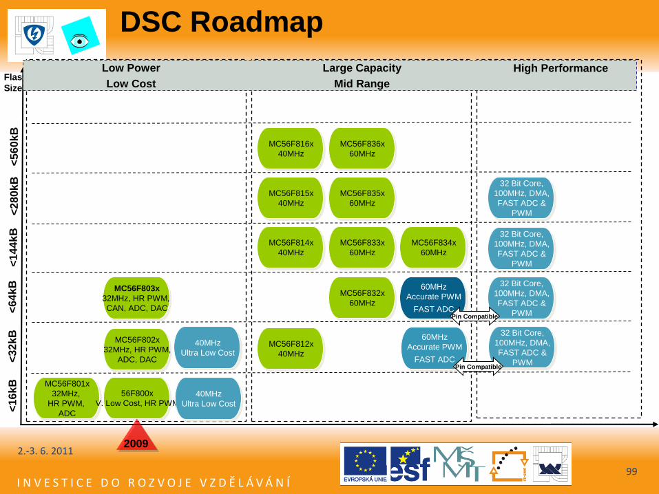
DSC Roadmap
2.-3. 6. 2011
99
MC56F802x
32MHz, HR PWM,
ADC, DAC
MC56F801x
32MHz,
HR PWM,
ADC
Flash
Size
32 Bit Core,
100MHz, DMA,
FAST ADC &
PWM
<1
6k
B
<3
2k
B
<1
44
kB
56F800x
V. Low Cost, HR PWM
<6
4k
B
MC56F803x
32MHz, HR PWM,
CAN, ADC, DAC
60MHz
Accurate PWM
FAST ADC
<2
80
kB
32 Bit Core,
100MHz, DMA,
FAST ADC &
PWM
40MHz
Ultra Low Cost
32 Bit Core,
100MHz, DMA,
FAST ADC &
PWM
32 Bit Core,
100MHz, DMA,
FAST ADC &
PWM
<5
60
kB
MC56F832x
60MHz
MC56F833x
60MHz
MC56F835x
60MHz
MC56F836x
60MHz
MC56F834x
60MHz
MC56F812x
40MHz
MC56F814x
40MHz
MC56F815x
40MHz
MC56F816x
40MHz
Low Power
Low Cost
Large Capacity
Mid Range
High Performance
Pin Compatible
40MHz
Ultra Low Cost
2009
60MHz
Accurate PWM
FAST ADC Pin Compatible
I N V E S T I C E D O R O Z V O J E V Z D Ě L Á V Á N Í
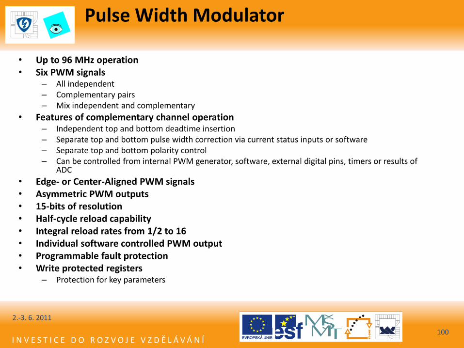
Pulse Width Modulator
2.-3. 6. 2011
100
• Up to 96 MHz operation • Six PWM signals
– All independent – Complementary pairs – Mix independent and complementary
• Features of complementary channel operation – Independent top and bottom deadtime insertion – Separate top and bottom pulse width correction via current status inputs or software – Separate top and bottom polarity control – Can be controlled from internal PWM generator, software, external digital pins, timers or results of
ADC
• Edge- or Center-Aligned PWM signals • Asymmetric PWM outputs • 15-bits of resolution • Half-cycle reload capability • Integral reload rates from 1/2 to 16 • Individual software controlled PWM output • Programmable fault protection • Write protected registers
– Protection for key parameters
I N V E S T I C E D O R O Z V O J E V Z D Ě L Á V Á N Í
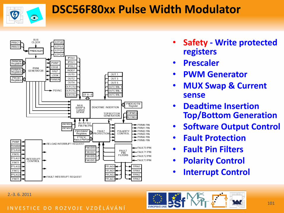
DSC56F80xx Pulse Width Modulator
2.-3. 6. 2011
101
• Safety - Write protected registers
• Prescaler • PWM Generator • MUX Swap & Current
sense • Deadtime Insertion
Top/Bottom Generation • Software Output Control • Fault Protection • Fault Pin Filters • Polarity Control • Interrupt Control
I N V E S T I C E D O R O Z V O J E V Z D Ě L Á V Á N Í
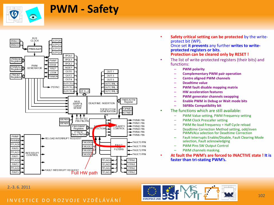
PWM - Safety
2.-3. 6. 2011
102
• Safety critical setting can be protected by the write-protect bit (WP). Once set it prevents any further writes to write-protected registers or bits. Protection can be cleared only by RESET !
• The list of write-protected registers (their bits) and functions:
– PWM polarity – Complementary PWM pair operation – Centre aligned PWM channels – Deadtime value – PWM fault disable mapping matrix – HW acceleration features – PWM generator channels swapping – Enable PWM in Debug or Wait mode bits – 56F80x Compatibility bit
• The functions which are still available: – PWM Value setting, PWM Frequency setting – PWM Clock Prescaller setting – PWM Re-load Frequency + Half Cycle reload – Deadtime Correction Method setting, odd/even
PWMVALx selection for Deadtime Correction – Fault Interrupts Enable/Disable, Fault Clearing Mode
selection, Fault acknowledging – PWM Pins SW Output Control – PWM channels masking.
• At fault the PWM’s are forced to INACTIVE state ! It is faster than tri-stating PWM’s.
Full HW path
I N V E S T I C E D O R O Z V O J E V Z D Ě L Á V Á N Í
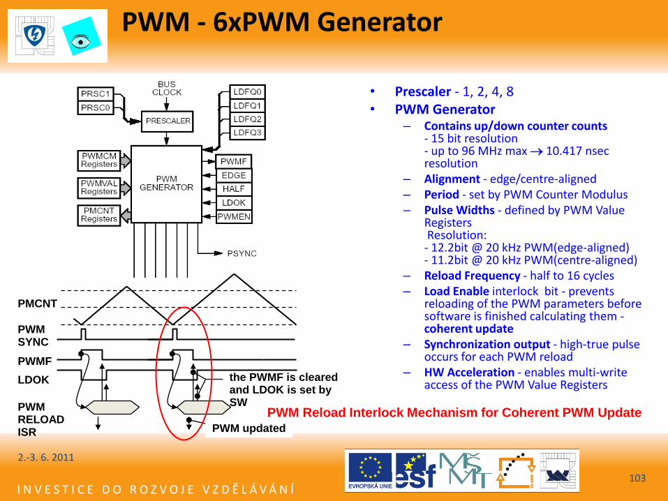
PWM - 6xPWM Generator
2.-3. 6. 2011
103
• Prescaler - 1, 2, 4, 8 • PWM Generator
– Contains up/down counter counts - 15 bit resolution - up to 96 MHz max 10.417 nsec resolution
– Alignment - edge/centre-aligned – Period - set by PWM Counter Modulus – Pulse Widths - defined by PWM Value
Registers Resolution: - 12.2bit @ 20 kHz PWM(edge-aligned) - 11.2bit @ 20 kHz PWM(centre-aligned)
– Reload Frequency - half to 16 cycles – Load Enable interlock bit - prevents
reloading of the PWM parameters before software is finished calculating them - coherent update
– Synchronization output - high-true pulse occurs for each PWM reload
– HW Acceleration - enables multi-write access of the PWM Value Registers LDOK
PWMF
PMCNT
PWM RELOAD ISR
PWM SYNC
PWM updated
the PWMF is cleared and LDOK is set by SW
PWM Reload Interlock Mechanism for Coherent PWM Update
I N V E S T I C E D O R O Z V O J E V Z D Ě L Á V Á N Í
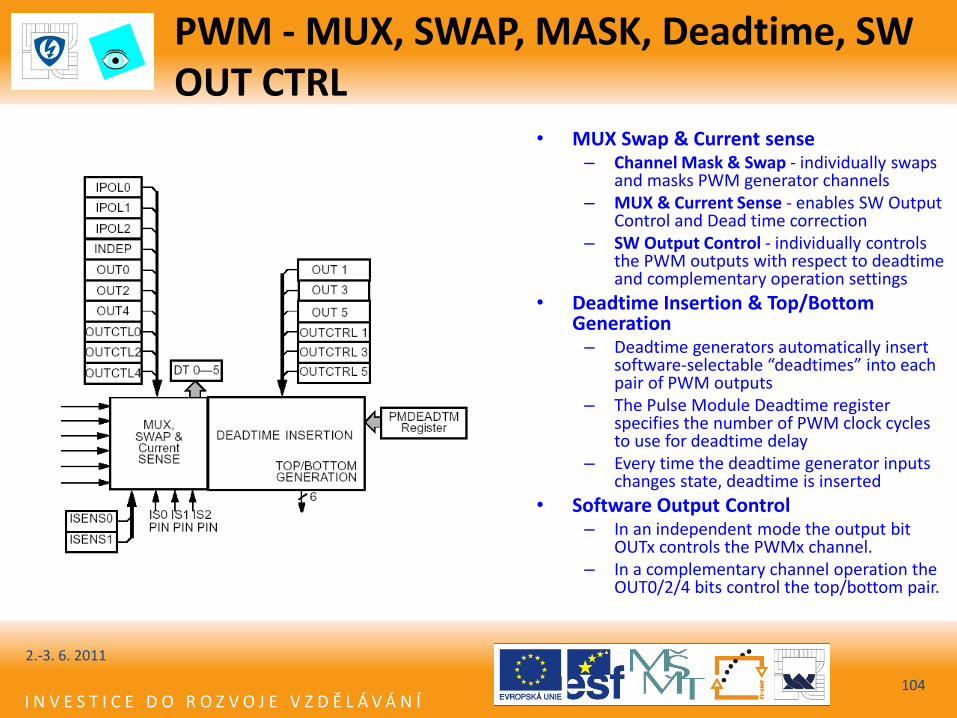
PWM - MUX, SWAP, MASK, Deadtime, SW OUT CTRL
2.-3. 6. 2011
104
• MUX Swap & Current sense – Channel Mask & Swap - individually swaps
and masks PWM generator channels – MUX & Current Sense - enables SW Output
Control and Dead time correction – SW Output Control - individually controls
the PWM outputs with respect to deadtime and complementary operation settings
• Deadtime Insertion & Top/Bottom Generation
– Deadtime generators automatically insert software-selectable “deadtimes” into each pair of PWM outputs
– The Pulse Module Deadtime register specifies the number of PWM clock cycles to use for deadtime delay
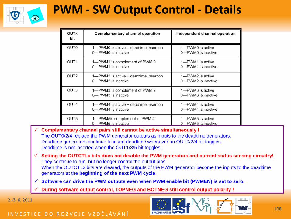
– Every time the deadtime generator inputs changes state, deadtime is inserted
• Software Output Control – In an independent mode the output bit
OUTx controls the PWMx channel. – In a complementary channel operation the
OUT0/2/4 bits control the top/bottom pair.
I N V E S T I C E D O R O Z V O J E V Z D Ě L Á V Á N Í
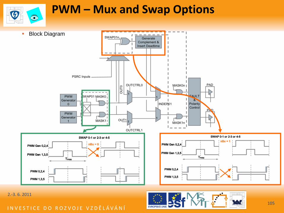
PWM – Mux and Swap Options
2.-3. 6. 2011
105
PWM
Generator
0
PWM
Generator
1
1
11
1
Generate
Complement &
Insert Deadtime
FAULT
&
Polarity
Control
PSRC Inputs
SWAP01n
OU
T0 OUTCTRL0
SWAP01 MASK0
MASK1 OUT1
OUTCTRL1
MASK0n
INDEP01
MASK1n
PAD
PAD
Block Diagram
PWM Gen 0,2,4
PWM Gen 1,3,5
PWM 0,2,4
PWM 1,3,5
TPWM
SWAP 0-1 or 2-3 or 4-5
nBx = 0 PWM Gen 0,2,4
PWM Gen 1,3,5
PWM 0,2,4
PWM 1,3,5
TPWM
SWAP 0-1 or 2-3 or 4-5
nBx = 1
I N V E S T I C E D O R O Z V O J E V Z D Ě L Á V Á N Í
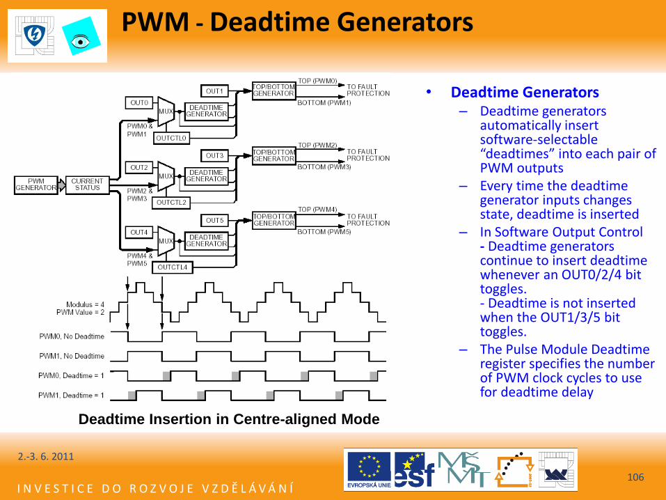
PWM - Deadtime Generators
2.-3. 6. 2011
106
• Deadtime Generators – Deadtime generators
automatically insert software-selectable “deadtimes” into each pair of PWM outputs
– Every time the deadtime generator inputs changes state, deadtime is inserted
– In Software Output Control - Deadtime generators continue to insert deadtime whenever an OUT0/2/4 bit toggles. - Deadtime is not inserted when the OUT1/3/5 bit toggles.
– The Pulse Module Deadtime register specifies the number of PWM clock cycles to use for deadtime delay
Deadtime Insertion in Centre-aligned Mode
I N V E S T I C E D O R O Z V O J E V Z D Ě L Á V Á N Í
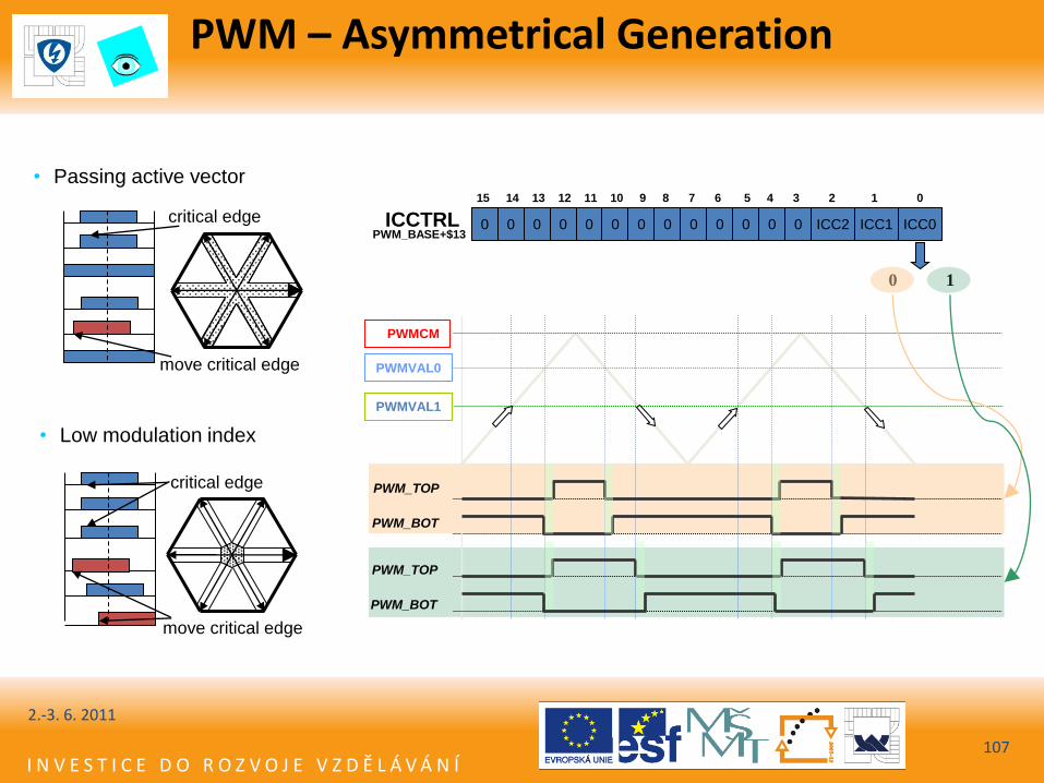
PWM – Asymmetrical Generation
2.-3. 6. 2011
107
ICC0 ICC1 ICC2 0 0 0 0 0 0 0 0 0 0 0 0 0 ICCTRL PWM_BASE+$13
15 14 13 12 11 10 9 8 7 6 5 4 3 2 1 0
PWMCM
PWMVAL0
PWMVAL1
PWM_TOP
PWM_BOT
PWM_TOP
PWM_BOT
0 1
critical edge
move critical edge
critical edge
move critical edge
• Passing active vector
• Low modulation index
I N V E S T I C E D O R O Z V O J E V Z D Ě L Á V Á N Í
PWM - SW Output Control - Details
2.-3. 6. 2011
108
Complementary channel pairs still cannot be active simultaneously !
The OUT0/2/4 replace the PWM generator outputs as inputs to the deadtime generators.
Deadtime generators continue to insert deadtime whenever an OUT0/2/4 bit toggles.
Deadtime is not inserted when the OUT1/3/5 bit toggles.
Setting the OUTCTLx bits does not disable the PWM generators and current status sensing circuitry!
They continue to run, but no longer control the output pins.
When the OUTCTLx bits are cleared, the outputs of the PWM generator become the inputs to the deadtime
generators at the beginning of the next PWM cycle.
Software can drive the PWM outputs even when PWM enable bit (PWMEN) is set to zero.
During software output control, TOPNEG and BOTNEG still control output polarity !
I N V E S T I C E D O R O Z V O J E V Z D Ě L Á V Á N Í
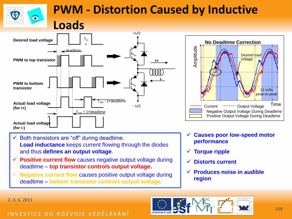
PWM - Distortion Caused by Inductive Loads
2.-3. 6. 2011
109
Both transistors are “off” during deadtime.
Load inductance keeps current flowing through the diodes
and thus defines an output voltage.
Positive current flow causes negative output voltage during
deadtime – top transistor controls output voltage.
Negative current flow causes positive output voltage during
deadtime – bottom transistor controls output voltage.
i+
i-
+U/2
- U/2
TON - 1×deadtime
Desired load voltage
PWM to top transistor
PWM to bottom transistor
Actual load voltage (for i+)
Actual load voltage (for i-)
TO
N
TON + 1×deadtime
deadtime
Causes poor low-speed motor performance
Torque ripple
Distorts current
Produces noise in audible region
No Deadtime Correction
Am
plit
ude
Time
Positive Output Voltage During Deadtime Negative Output Voltage During Deadtime
Current Output Voltage
12 volts
peak-to-peak
Desired load voltage
I N V E S T I C E D O R O Z V O J E V Z D Ě L Á V Á N Í
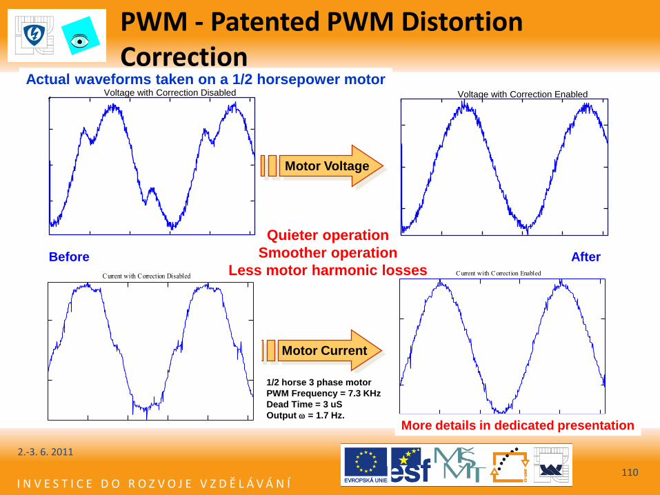
Actual waveforms taken on a 1/2 horsepower motor
PWM - Patented PWM Distortion Correction
2.-3. 6. 2011
110
Voltage with Correction Disabled
Current with Correction Disabled Current with Correction Enabled
Voltage with Correction Enabled
Before After
Motor Current
Quieter operation
Smoother operation
Less motor harmonic losses
Motor Voltage
1/2 horse 3 phase motor
PWM Frequency = 7.3 KHz
Dead Time = 3 uS
Output = 1.7 Hz.
More details in dedicated presentation
I N V E S T I C E D O R O Z V O J E V Z D Ě L Á V Á N Í
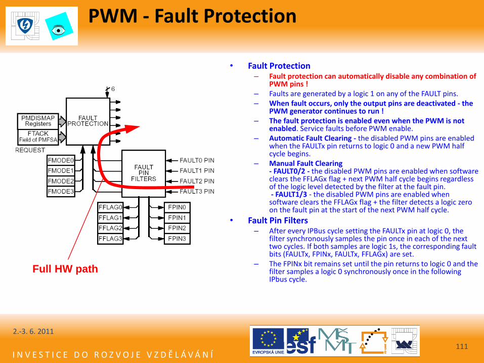
PWM - Fault Protection
2.-3. 6. 2011
111
• Fault Protection – Fault protection can automatically disable any combination of
PWM pins ! – Faults are generated by a logic 1 on any of the FAULT pins. – When fault occurs, only the output pins are deactivated - the
PWM generator continues to run ! – The fault protection is enabled even when the PWM is not
enabled. Service faults before PWM enable. – Automatic Fault Clearing - the disabled PWM pins are enabled
when the FAULTx pin returns to logic 0 and a new PWM half cycle begins.
– Manual Fault Clearing - FAULT0/2 - the disabled PWM pins are enabled when software clears the FFLAGx flag + next PWM half cycle begins regardless of the logic level detected by the filter at the fault pin. - FAULT1/3 - the disabled PWM pins are enabled when software clears the FFLAGx flag + the filter detects a logic zero on the fault pin at the start of the next PWM half cycle.
• Fault Pin Filters – After every IPBus cycle setting the FAULTx pin at logic 0, the
filter synchronously samples the pin once in each of the next two cycles. If both samples are logic 1s, the corresponding fault bits (FAULTx, FPINx, FAULTx, FFLAGx) are set.
– The FPINx bit remains set until the pin returns to logic 0 and the filter samples a logic 0 synchronously once in the following IPbus cycle.
Full HW path
I N V E S T I C E D O R O Z V O J E V Z D Ě L Á V Á N Í
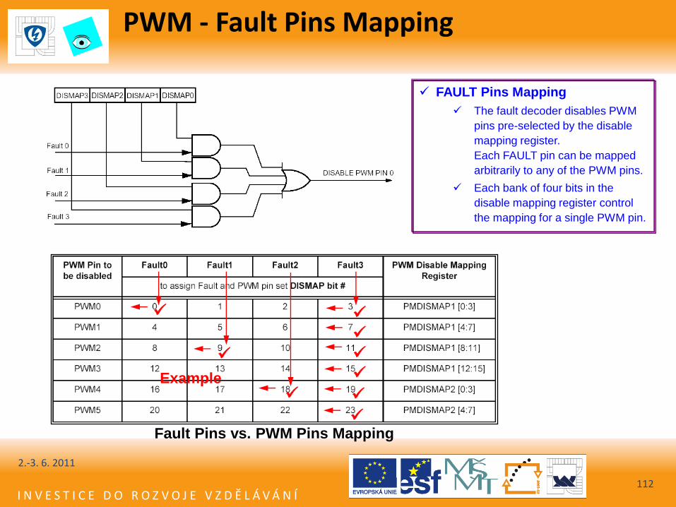
PWM - Fault Pins Mapping
2.-3. 6. 2011
112
FAULT Pins Mapping
The fault decoder disables PWM
pins pre-selected by the disable
mapping register.
Each FAULT pin can be mapped
arbitrarily to any of the PWM pins.
Each bank of four bits in the
disable mapping register control
the mapping for a single PWM pin.
Fault Pins vs. PWM Pins Mapping
Example
I N V E S T I C E D O R O Z V O J E V Z D Ě L Á V Á N Í
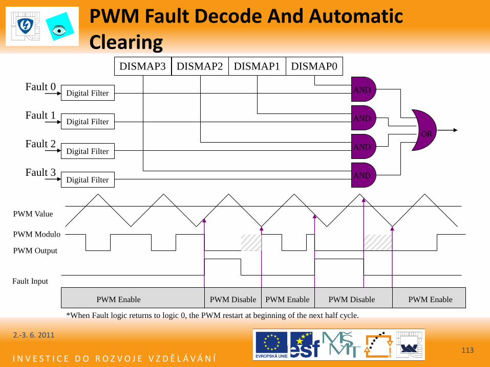
PWM Fault Decode And Automatic Clearing
2.-3. 6. 2011
113
AND
AND
AND
AND
OR
DISMAP3 DISMAP2 DISMAP1 DISMAP0
Digital Filter
Digital Filter
Digital Filter
Digital Filter
Fault 0
Fault 1
Fault 2
Fault 3
PWM Enable PWM Disable PWM Enable PWM Disable PWM Enable
PWM Output
PWM Modulo
PWM Value
Fault Input
*When Fault logic returns to logic 0, the PWM restart at beginning of the next half cycle.
I N V E S T I C E D O R O Z V O J E V Z D Ě L Á V Á N Í
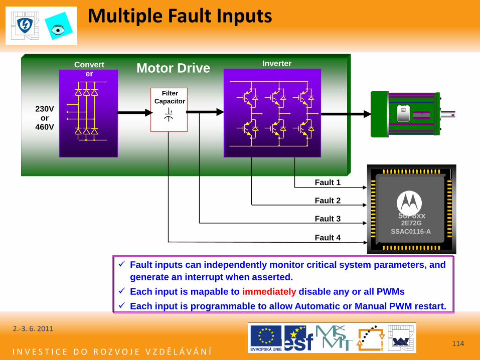
Multiple Fault Inputs
2.-3. 6. 2011
114
Filter Capacitor
Converter
230V or
460V
Inverter Motor Drive
2E72G 56F8xx
SSAC0116-A
Fault 1
Fault 2
Fault 3
Fault 4
Fault inputs can independently monitor critical system parameters, and
generate an interrupt when asserted.
Each input is mapable to immediately disable any or all PWMs
Each input is programmable to allow Automatic or Manual PWM restart.
M
Motorola
Dave’s Control Center
I N V E S T I C E D O R O Z V O J E V Z D Ě L Á V Á N Í
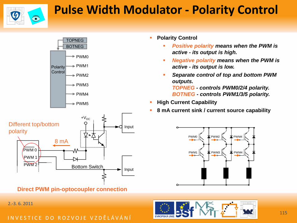
Pulse Width Modulator - Polarity Control
2.-3. 6. 2011
115
Direct PWM pin-optocoupler connection
PWM 0
PWM 1
PWM 2
8 mA
Bottom Switch
Input
+VDC
Input
Different top/bottom
polarity
Polarity
Control
PWM0
PWM1
PWM2
PWM3
PWM4
PWM5
BOTNEG
TOPNEG Polarity Control
Positive polarity means when the PWM is
active - its output is high.
Negative polarity means when the PWM is
active - its output is low.
Separate control of top and bottom PWM
outputs.
TOPNEG - controls PWM0/2/4 polarity.
BOTNEG - controls PWM1/3/5 polarity.
High Current Capability
8 mA current sink / current source capability
PWM0 PWM2 PWM4
PWM1 PWM3 PWM4
I N V E S T I C E D O R O Z V O J E V Z D Ě L Á V Á N Í
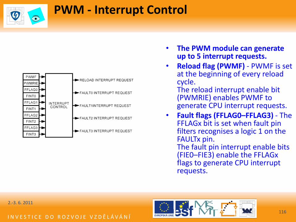
PWM - Interrupt Control
2.-3. 6. 2011
116
• The PWM module can generate up to 5 interrupt requests.
• Reload flag (PWMF) - PWMF is set at the beginning of every reload cycle. The reload interrupt enable bit (PWMRIE) enables PWMF to generate CPU interrupt requests.
• Fault flags (FFLAG0–FFLAG3) - The FFLAGx bit is set when fault pin filters recognises a logic 1 on the FAULTx pin. The fault pin interrupt enable bits (FIE0–FIE3) enable the FFLAGx flags to generate CPU interrupt requests.
I N V E S T I C E D O R O Z V O J E V Z D Ě L Á V Á N Í
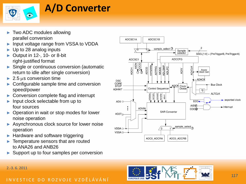
A/D Converter
117
► Two ADC modules allowing
parallel conversion
► Input voltage range from VSSA to VDDA
► Up to 28 analog inputs
► Output in 12-, 10- or 8-bit
right-justified format
► Single or continuous conversion (automatic
return to idle after single conversion)
► 2.5 ms conversion time
► Configurable sample time and conversion
speed/power
► Conversion complete flag and interrupt
► Input clock selectable from up to
four sources
► Operation in wait or stop modes for lower
noise operation
► Asynchronous clock source for lower noise
operation
► Hardware and software triggering
► Temperature sensors that are routed
to ANA26 and ANB26
► Support up to four samples per conversion
2.-3. 6. 2011
I N V E S T I C E D O R O Z V O J E V Z D Ě L Á V Á N Í
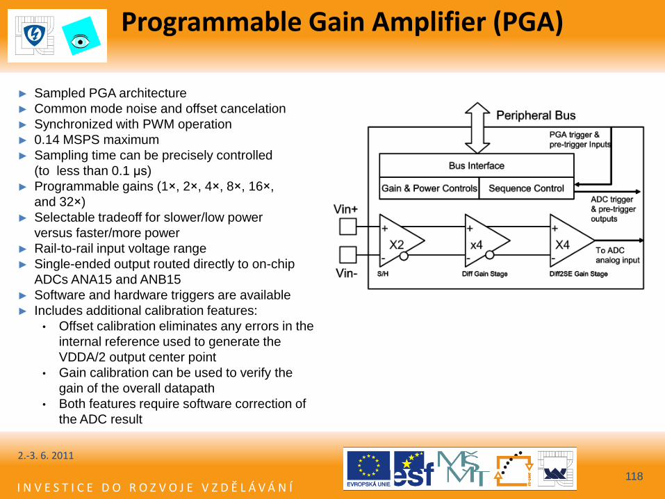
Programmable Gain Amplifier (PGA)
118
► Sampled PGA architecture
► Common mode noise and offset cancelation
► Synchronized with PWM operation
► 0.14 MSPS maximum
► Sampling time can be precisely controlled
(to less than 0.1 μs)
► Programmable gains (1×, 2×, 4×, 8×, 16×,
and 32×)
► Selectable tradeoff for slower/low power
versus faster/more power
► Rail-to-rail input voltage range
► Single-ended output routed directly to on-chip
ADCs ANA15 and ANB15
► Software and hardware triggers are available
► Includes additional calibration features:
• Offset calibration eliminates any errors in the
internal reference used to generate the
VDDA/2 output center point
• Gain calibration can be used to verify the
gain of the overall datapath
• Both features require software correction of
the ADC result
2.-3. 6. 2011
I N V E S T I C E D O R O Z V O J E V Z D Ě L Á V Á N Í
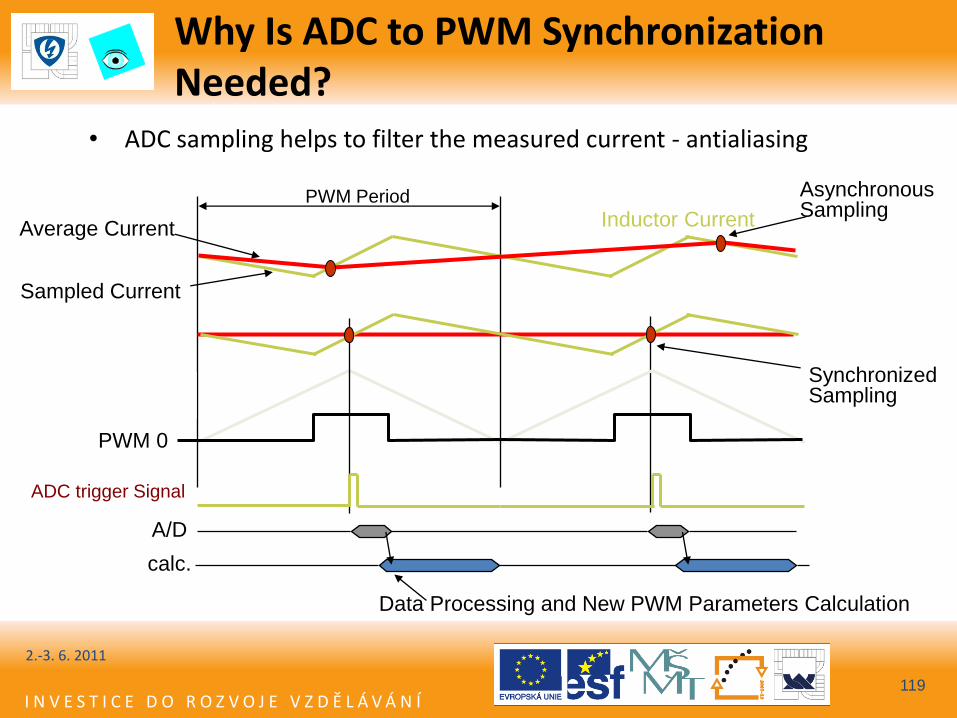
Why Is ADC to PWM Synchronization Needed?
• ADC sampling helps to filter the measured current - antialiasing
119
PWM Period
PWM 0
Inductor Current Average Current
A/D
calc.
Data Processing and New PWM Parameters Calculation
ADC trigger Signal
Sampled Current
Asynchronous Sampling
Synchronized Sampling
2.-3. 6. 2011
I N V E S T I C E D O R O Z V O J E V Z D Ě L Á V Á N Í
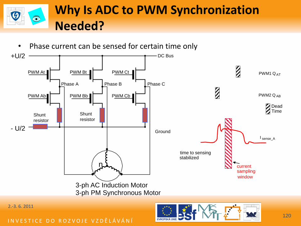
Why Is ADC to PWM Synchronization Needed?
• Phase current can be sensed for certain time only
120
PWM Bt PWM Ct PWM At
Phase A Phase B Phase C
DC Bus
Ground
Shunt
resistor
n
+U/2
- U/2
PWM Bb PWM Cb PWM Ab
3-ph AC Induction Motor 3-ph PM Synchronous Motor
Shunt
resistor
time to sensing
current
Dead Time
stabilized
sampling
PWM1 Q AT
PWM2 Q AB
I sense_A
window
2.-3. 6. 2011
I N V E S T I C E D O R O Z V O J E V Z D Ě L Á V Á N Í
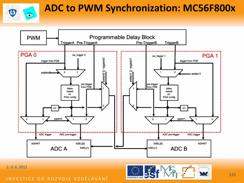
ADC to PWM Synchronization: MC56F800x
121
2.-3. 6. 2011
I N V E S T I C E D O R O Z V O J E V Z D Ě L Á V Á N Í
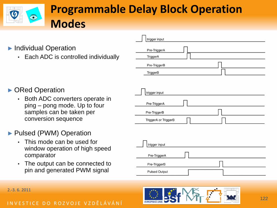
Programmable Delay Block Operation Modes
122
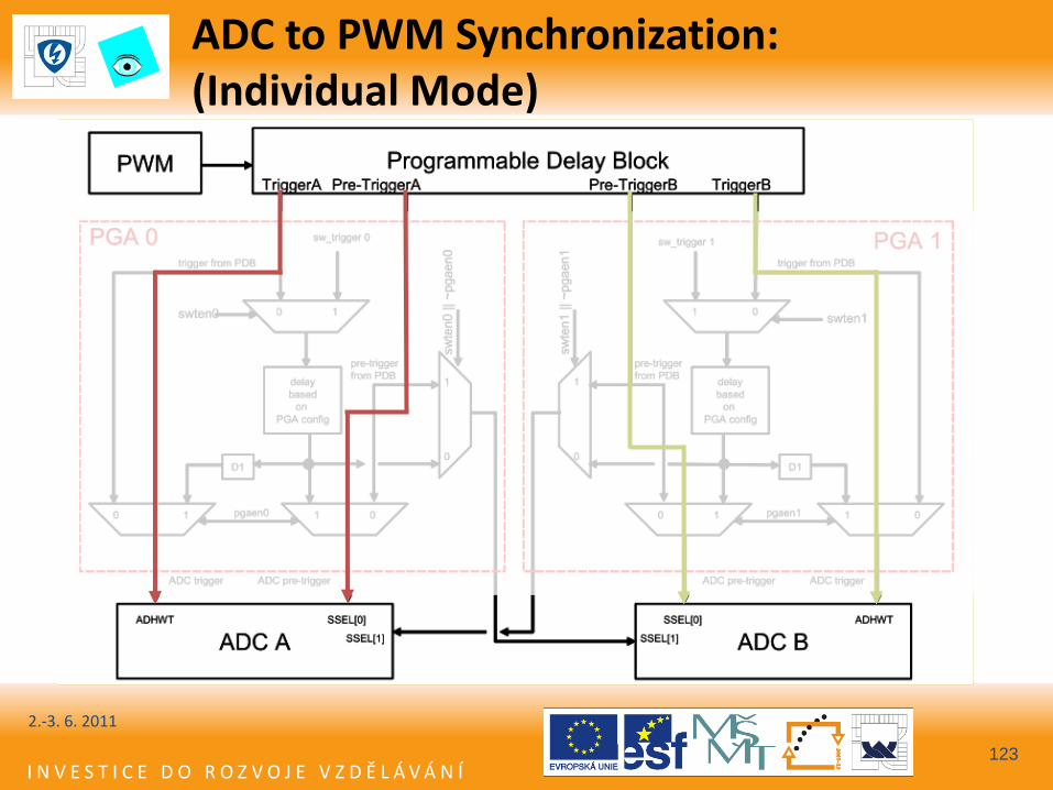
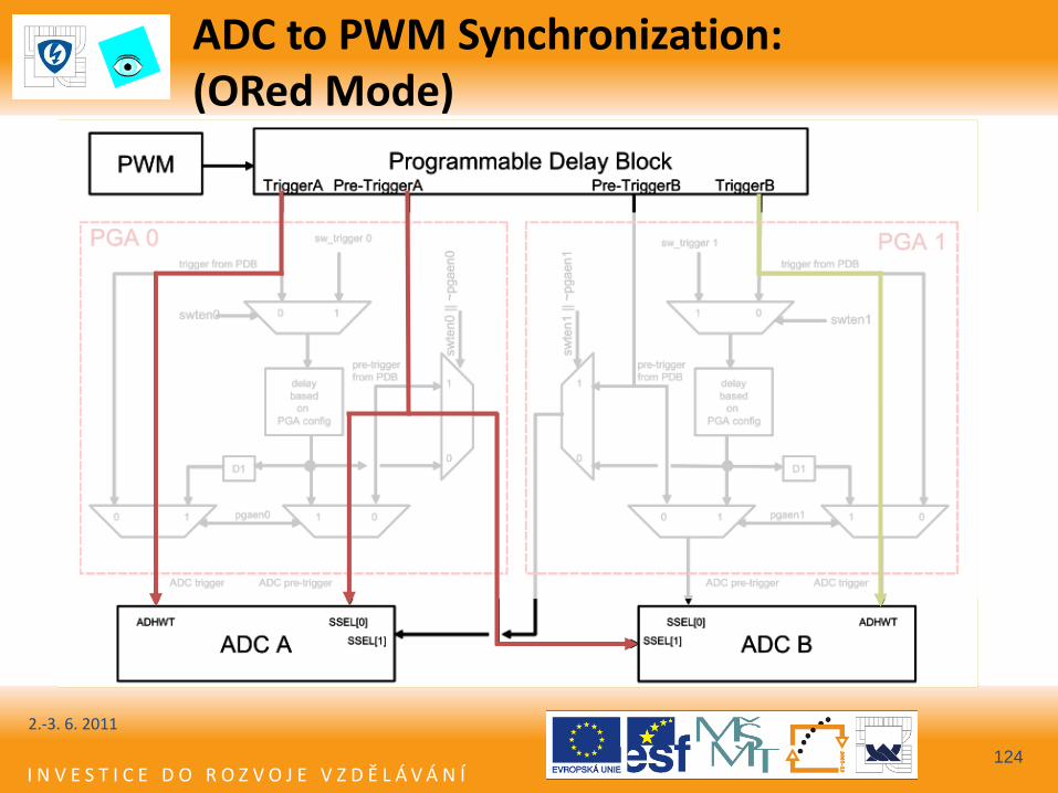
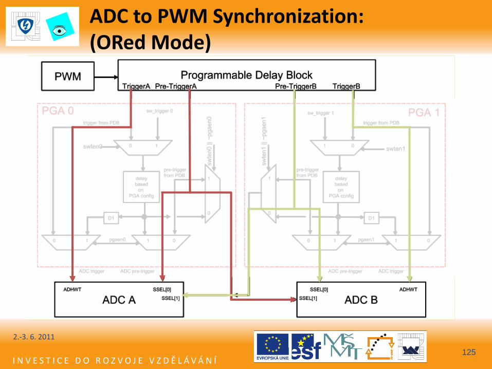
► Individual Operation
• Each ADC is controlled individually
► ORed Operation
• Both ADC converters operate in ping – pong mode. Up to four samples can be taken per conversion sequence
► Pulsed (PWM) Operation
• This mode can be used for window operation of high speed comparator
• The output can be connected to pin and generated PWM signal
2.-3. 6. 2011
I N V E S T I C E D O R O Z V O J E V Z D Ě L Á V Á N Í
ADC to PWM Synchronization: (Individual Mode)
123
2.-3. 6. 2011
I N V E S T I C E D O R O Z V O J E V Z D Ě L Á V Á N Í
ADC to PWM Synchronization: (ORed Mode)
124
2.-3. 6. 2011
I N V E S T I C E D O R O Z V O J E V Z D Ě L Á V Á N Í
ADC to PWM Synchronization: (ORed Mode)
125
2.-3. 6. 2011
I N V E S T I C E D O R O Z V O J E V Z D Ě L Á V Á N Í
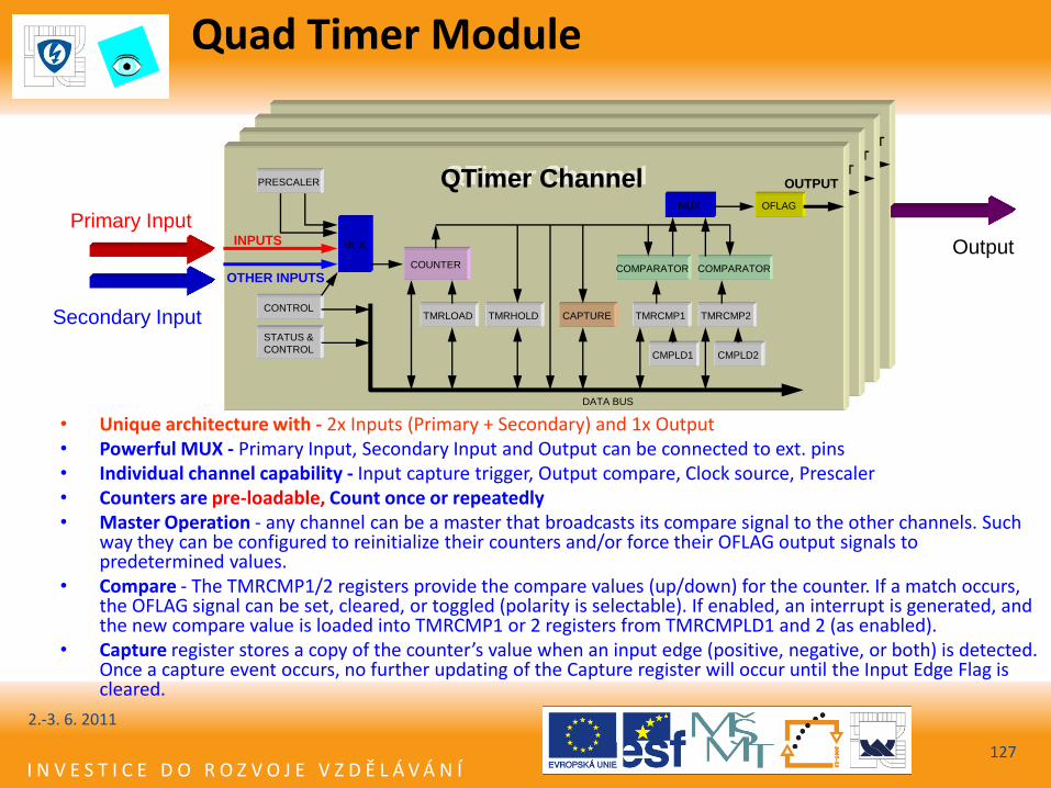
Quad Timer Module
2.-3. 6. 2011
126
• 4x 16-bit general purpose up/down timer/counters per module • Up to 96 MHz operation • Individual channel capability
– Input capture trigger – Output compare – Clock source – Prescaler
• Max. count rate – external events counting - peripheral clock/2 – internal clock counting - peripheral clock
• Counters are pre-loadable • Count once or repeatedly • Programmable count modulo • Input pins are fully shareable within timer module • Pins available as general I/O when timer(s) not in use • Counters in module can be daisy-chained to yield longer counter lengths • Master operation
– “Broadcasts” compare function – channel re-initialization for coherent operation
• Up to 12 operation Modes
I N V E S T I C E D O R O Z V O J E V Z D Ě L Á V Á N Í
Quad Timer Module
2.-3. 6. 2011
127
• Unique architecture with - 2x Inputs (Primary + Secondary) and 1x Output • Powerful MUX - Primary Input, Secondary Input and Output can be connected to ext. pins • Individual channel capability - Input capture trigger, Output compare, Clock source, Prescaler • Counters are pre-loadable, Count once or repeatedly • Master Operation - any channel can be a master that broadcasts its compare signal to the other channels. Such
way they can be configured to reinitialize their counters and/or force their OFLAG output signals to predetermined values.
• Compare - The TMRCMP1/2 registers provide the compare values (up/down) for the counter. If a match occurs, the OFLAG signal can be set, cleared, or toggled (polarity is selectable). If enabled, an interrupt is generated, and the new compare value is loaded into TMRCMP1 or 2 registers from TMRCMPLD1 and 2 (as enabled).
• Capture register stores a copy of the counter’s value when an input edge (positive, negative, or both) is detected. Once a capture event occurs, no further updating of the Capture register will occur until the Input Edge Flag is cleared.
PRESCALER
MUX
CONTROL
COUNTER
TMRLOAD TMRHOLD CAPTURE TMRCMP1 TMRCMP2
CMPLD1 CMPLD2
COMPARATOR COMPARATOR
MUX OFLAG
OUTPUT
INPUTS
OTHER INPUTS
STATUS &
CONTROL
DATA BUS
QTimer Channel PRESCALER
MUX
CONTROL
COUNTER
TMRLOAD TMRHOLD CAPTURE TMRCMP1 TMRCMP2
CMPLD1 CMPLD2
COMPARATOR COMPARATOR
MUX OFLAG
OUTPUT
INPUTS
OTHER INPUTS
STATUS &
CONTROL
DATA BUS
QTimer Channel PRESCALER
MUX
CONTROL
COUNTER
TMRLOAD TMRHOLD CAPTURE TMRCMP1 TMRCMP2
CMPLD1 CMPLD2
COMPARATOR COMPARATOR
MUX OFLAG
OUTPUT
INPUTS
OTHER INPUTS
STATUS &
CONTROL
DATA BUS
QTimer Channel
Primary Input
Secondary Input
PRESCALER
MUX
CONTROL
COUNTER
TMRLOAD TMRHOLD CAPTURE TMRCMP1 TMRCMP2
CMPLD1 CMPLD2
COMPARATOR COMPARATOR
MUX OFLAG
OUTPUT
INPUTS
OTHER INPUTS
STATUS &
CONTROL
DATA BUS
QTimer Channel
Output
I N V E S T I C E D O R O Z V O J E V Z D Ě L Á V Á N Í
Quad Timer Module
2.-3. 6. 2011
128
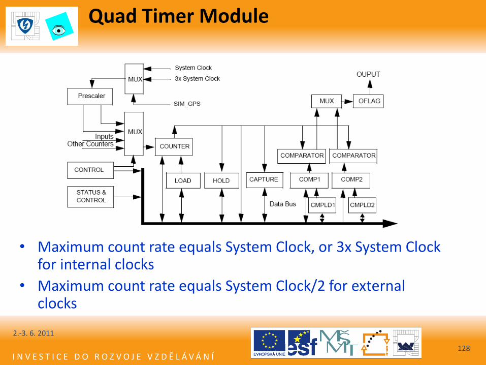
• Maximum count rate equals System Clock, or 3x System Clock for internal clocks
• Maximum count rate equals System Clock/2 for external clocks
I N V E S T I C E D O R O Z V O J E V Z D Ě L Á V Á N Í
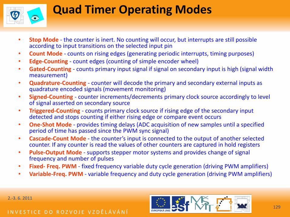
Quad Timer Operating Modes
2.-3. 6. 2011
129
• Stop Mode - the counter is inert. No counting will occur, but interrupts are still possible according to input transitions on the selected input pin
• Count Mode - counts on rising edges (generating periodic interrupts, timing purposes) • Edge-Counting - count edges (counting of simple encoder wheel) • Gated-Counting - counts primary input signal if signal on secondary input is high (signal width
measurement) • Quadrature-Counting - counter will decode the primary and secondary external inputs as
quadrature encoded signals (movement monitoring) • Signed-Counting - counter increments/decrements primary clock source accordingly to level
of signal asserted on secondary source • Triggered-Counting - counts primary clock source if rising edge of the secondary input
detected and stops counting if either rising edge or compare event occurs • One-Shot Mode - provides timing delays (ADC acquisition of new samples until a specified
period of time has passed since the PWM sync signal) • Cascade-Count Mode - the counter’s input is connected to the output of another selected
counter. If any counter is read the values of other counters are captured in hold registers • Pulse-Output Mode - supports stepper motor systems and provides change of signal
frequency and number of pulses • Fixed- Freq. PWM - fixed frequency variable duty cycle generation (driving PWM amplifiers) • Variable-Freq. PWM - variable frequency and duty cycle generation (driving PWM amplifiers)
I N V E S T I C E D O R O Z V O J E V Z D Ě L Á V Á N Í
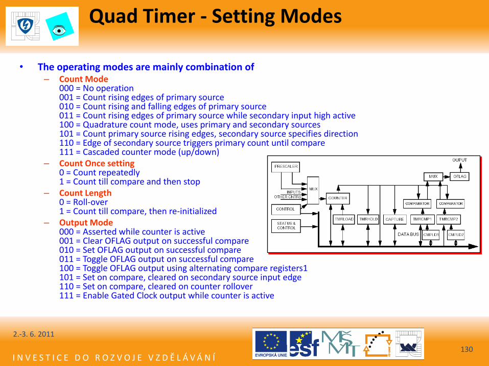
Quad Timer - Setting Modes
2.-3. 6. 2011
130
• The operating modes are mainly combination of – Count Mode
000 = No operation 001 = Count rising edges of primary source 010 = Count rising and falling edges of primary source 011 = Count rising edges of primary source while secondary input high active 100 = Quadrature count mode, uses primary and secondary sources 101 = Count primary source rising edges, secondary source specifies direction 110 = Edge of secondary source triggers primary count until compare 111 = Cascaded counter mode (up/down)
– Count Once setting 0 = Count repeatedly 1 = Count till compare and then stop
– Count Length 0 = Roll-over 1 = Count till compare, then re-initialized
– Output Mode 000 = Asserted while counter is active 001 = Clear OFLAG output on successful compare 010 = Set OFLAG output on successful compare 011 = Toggle OFLAG output on successful compare 100 = Toggle OFLAG output using alternating compare registers1 101 = Set on compare, cleared on secondary source input edge 110 = Set on compare, cleared on counter rollover 111 = Enable Gated Clock output while counter is active
I N V E S T I C E D O R O Z V O J E V Z D Ě L Á V Á N Í
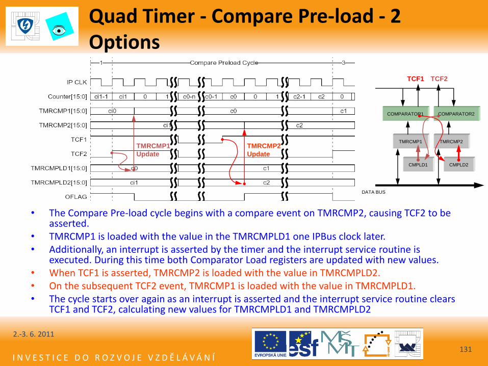
Quad Timer - Compare Pre-load - 2 Options
2.-3. 6. 2011
131
• The Compare Pre-load cycle begins with a compare event on TMRCMP2, causing TCF2 to be asserted.
• TMRCMP1 is loaded with the value in the TMRCMPLD1 one IPBus clock later. • Additionally, an interrupt is asserted by the timer and the interrupt service routine is
executed. During this time both Comparator Load registers are updated with new values. • When TCF1 is asserted, TMRCMP2 is loaded with the value in TMRCMPLD2. • On the subsequent TCF2 event, TMRCMP1 is loaded with the value in TMRCMPLD1. • The cycle starts over again as an interrupt is asserted and the interrupt service routine clears
TCF1 and TCF2, calculating new values for TMRCMPLD1 and TMRCMPLD2
TMRCMP2
Update
TMRCMP1
Update
TMRCMP1 TMRCMP2
CMPLD1 CMPLD2
COMPARATOR1 COMPARATOR2
DATA BUS
TCF1 TCF2
I N V E S T I C E D O R O Z V O J E V Z D Ě L Á V Á N Í
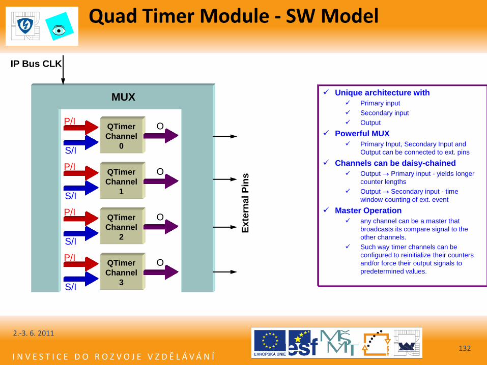
Quad Timer Module - SW Model
2.-3. 6. 2011
132
Unique architecture with
Primary input
Secondary input
Output
Powerful MUX
Primary Input, Secondary Input and
Output can be connected to ext. pins
Channels can be daisy-chained
Output Primary input - yields longer
counter lengths
Output Secondary input - time
window counting of ext. event
Master Operation
any channel can be a master that
broadcasts its compare signal to the
other channels.
Such way timer channels can be
configured to reinitialize their counters
and/or force their output signals to
predetermined values.
P/I
S/I
O QTimer
Channel
0
P/I
S/I
O QTimer
Channel
1
P/I
S/I
O QTimer
Channel
2
P/I
S/I
O QTimer
Channel
3
MUX
Ex
tern
al P
ins
IP Bus CLK
I N V E S T I C E D O R O Z V O J E V Z D Ě L Á V Á N Í
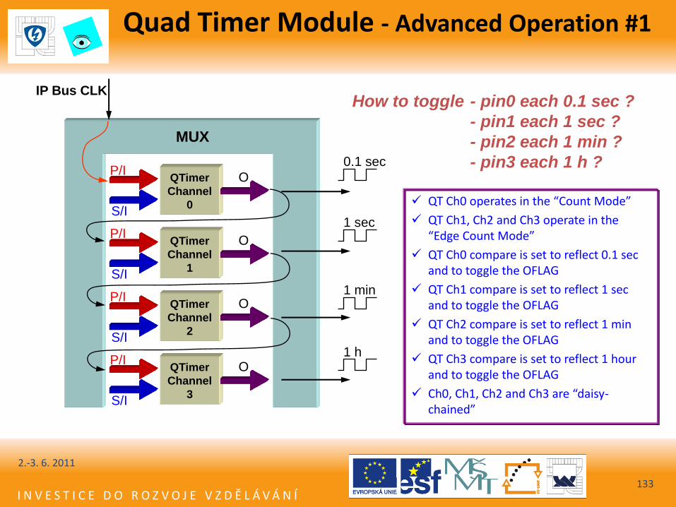
Quad Timer Module - Advanced Operation #1
2.-3. 6. 2011
133
P/I
S/I
O QTimer
Channel
0
P/I
S/I
O QTimer
Channel
1
P/I
S/I
O QTimer
Channel
2
P/I
S/I
O QTimer
Channel
3
MUX
IP Bus CLK How to toggle - pin0 each 0.1 sec ?
- pin1 each 1 sec ?
- pin2 each 1 min ?
- pin3 each 1 h ?
QT Ch0 operates in the “Count Mode”
QT Ch1, Ch2 and Ch3 operate in the “Edge Count Mode”
QT Ch0 compare is set to reflect 0.1 sec and to toggle the OFLAG
QT Ch1 compare is set to reflect 1 sec and to toggle the OFLAG
QT Ch2 compare is set to reflect 1 min and to toggle the OFLAG
QT Ch3 compare is set to reflect 1 hour and to toggle the OFLAG
Ch0, Ch1, Ch2 and Ch3 are “daisy-chained”
0.1 sec
1 sec
1 min
1 h
I N V E S T I C E D O R O Z V O J E V Z D Ě L Á V Á N Í
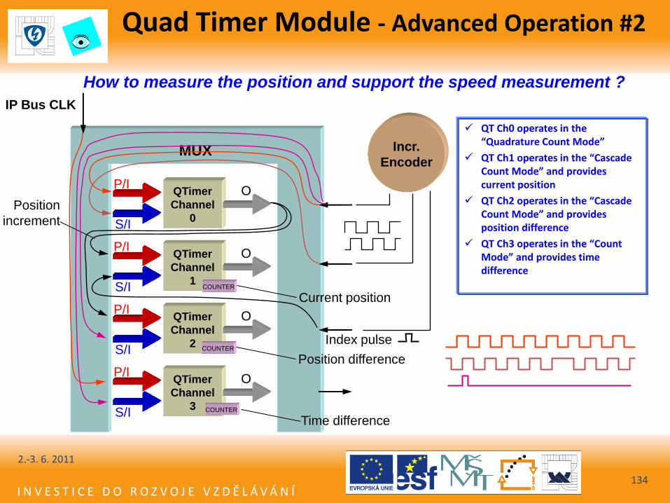
Quad Timer Module - Advanced Operation #2
2.-3. 6. 2011
134
P/I
S/I
O QTimer
Channel
0
P/I
S/I
O QTimer
Channel
1
P/I
S/I
O QTimer
Channel
2
P/I
S/I
O QTimer
Channel
3
MUX
IP Bus CLK
Incr.
Encoder
How to measure the position and support the speed measurement ?
Position
increment
Position difference COUNTER
QT Ch0 operates in the “Quadrature Count Mode”
QT Ch1 operates in the “Cascade Count Mode” and provides current position
QT Ch2 operates in the “Cascade Count Mode” and provides position difference
QT Ch3 operates in the “Count Mode” and provides time difference
Index pulse
Time difference COUNTER
Current position COUNTER
I N V E S T I C E D O R O Z V O J E V Z D Ě L Á V Á N Í
Programmable Interval Timer
2.-3. 6. 2011
135
• Three 16-bit general purpose up counter with a 4-bit prescaler
• Individually programmable time interval based on system clock source
• Counter roll-over generates interrupt request if roll-over interrupt is enabled
• Counter roll-over signal can be used as DAC conversion start signal.
• All PITs can be synchronized with PIT0
• Low Power Mode support
I N V E S T I C E D O R O Z V O J E V Z D Ě L Á V Á N Í
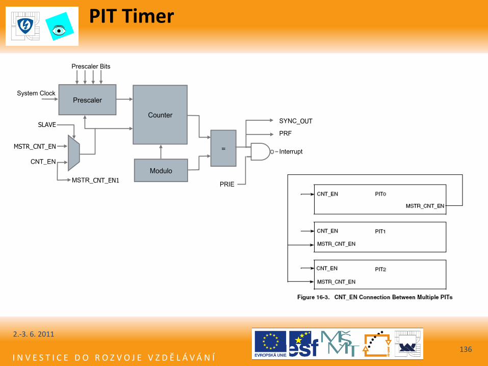
PIT Timer
2.-3. 6. 2011
136
Counter
Prescaler
Modulo
=
SLAVE
MSTR_CNT_EN
CNT_EN
System Clock
Prescaler Bits
MSTR_CNT_EN1PRIE
Interrupt
PRF
SYNC_OUT
I N V E S T I C E D O R O Z V O J E V Z D Ě L Á V Á N Í
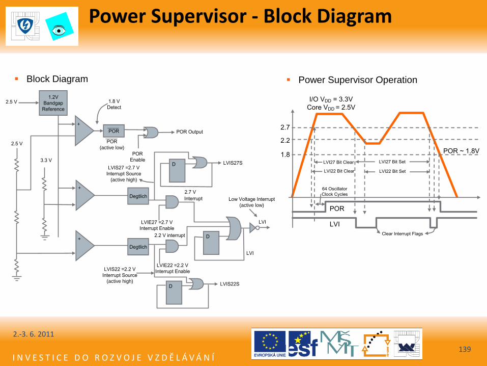
COP and Power Supervisor
2.-3. 6. 2011
137
• Computer Operating Properly – Free-running down counter that resets the device once the terminal count has been
reached – Can be used as a mechanism for recovering from errant software. – Has an associated reset vector in the interrupt vector table – Allows COP Resets to be handled differently than Hardware or Software Resets. – Features write-protectible registers for added protection. – Capable of selecting different clock sources to prevent primary clock failure caused
safety concerns – The service procedure consists of writing $5555 followed by $AAAA to the CNTR register.
• Power Supervisor
– Holds device in reset until there is enough voltage (VDD > 1.8V) for on-chip logic to operate at the oscillator frequency
• Precludes any problems associated with false restart
– Low Voltage detectors generate high-priority interrupts • Two low voltage detect signals used to initiate a software controlled shutdown when the supply
voltage drops below acceptable either 2.2V or 2.7V levels
– Eliminates need for external power monitor
I N V E S T I C E D O R O Z V O J E V Z D Ě L Á V Á N Í
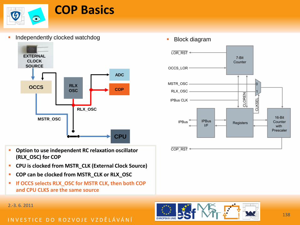
COP Basics
2.-3. 6. 2011
138
CPU
COP OCCS RLX
OSC
ADC
MSTR_OSC
RLX_OSC
7-Bit
Counter
Registers
0
1
16-Bit
Counter
with
Prescaler
IPBus
I/F
CLK
SE
L
CLO
RE
N
IPBus
COP_RST
IPBus CLK
RLX_OSC
MSTR_OSC
OCCS_LOR
LOR_RST
Independently clocked watchdog Block diagram
EXTERNAL
CLOCK
SOURCE
Option to use independent RC relaxation oscillator (RLX_OSC) for COP
CPU is clocked from MSTR_CLK (External Clock Source)
COP can be clocked from MSTR_CLK or RLX_OSC
If OCCS selects RLX_OSC for MSTR CLK, then both COP and CPU CLKS are the same source
I N V E S T I C E D O R O Z V O J E V Z D Ě L Á V Á N Í
Power Supervisor - Block Diagram
2.-3. 6. 2011
139
Block Diagram
1.2V
Bandgap
Reference
+
+
+
Degtlich
Degtlich
POR
D
D
D
2.5 V
2.5 V 1.8 V
Detect
POR
(active low)
POR Output
POR
Enable
LVIS27 =2.7 V
Interrupt Source
(active high)
LVIS27S
LVIE27 =2.7 V
Interrupt Enable
2.7 V
Interrupt Low Voltage Interrupt
(active low)
LVI
LVI
LVIS22S
2.2 V interrupt
LVIE22 =2.2 V
Interrupt EnableLVIS22 =2.2 V
Interrupt Source
(active high)
3.3 V
Power Supervisor Operation
2.7
2.2
1.8
I/O VDD = 3.3V
Core VDD = 2.5V
LVI
POR
LVI27 Bit Clear
LVI22 Bit Clear
POR ~ 1.8V
LVI27 Bit Set
LVI22 Bit Set
Clear Interrupt Flags
64 Oscillator
Clock Cycles

I N V E S T I C E D O R O Z V O J E V Z D Ě L Á V Á N Í
Thank you
2.-3. 6. 2011
140