Embed Size (px)
Citation preview
Quantum Oscillations in GrapheneRings
Bachelor’s Thesis in Physics
presented by
Florian Vennborn in Bottrop
Submitted to the Faculty of Mathematics, Computer Science and NaturalSciences of RWTH Aachen
under the supervision of
Prof. Dr. Hassler
Institute of Quantum Information
and
Prof. Dr. Stampfer
2nd Institute of Physics A
17.7.2015


iii
Ich versichere, dass ich die Arbeit selbstandig verfasst und keine anderen alsdie angegebenen Quellen und Hilfsmittel benutzt sowie Zitate kenntlich gemachthabe.
Aachen, 17.7.2015

iv
Abstract
The goal of this thesis is to understand a measured conductancetrace of a graphene ring. A prominent feature that was observedresembles a step. We discuss different possible origins with computersimulations. Beginning with the effect of conductance quantizationthat leads to steps visible in the simulation. We argue that this kindof modulation is not present in the experimental data. Next, westudy the signatures created by the classical transport properties ofthe system and compare the results with the experiment. We presentsimulation results that suggest that the observed effect is of classicnature.
v

vi ABSTRACT
Contents
Abstract v
1 Introduction to graphene 11.1 Graphene lattice . . . . . . . . . . . . . . . . . . . . . . . . . . . 11.2 Dispersion relation . . . . . . . . . . . . . . . . . . . . . . . . . . 21.3 Classical motion . . . . . . . . . . . . . . . . . . . . . . . . . . . 61.4 Landau levels . . . . . . . . . . . . . . . . . . . . . . . . . . . . . 7
2 Simulation methods 112.1 Tight-binding simulation . . . . . . . . . . . . . . . . . . . . . . . 112.2 Tracing of the classical trajectories . . . . . . . . . . . . . . . . . 13
3 Connection to the ring 153.1 Zig-zag and armchair . . . . . . . . . . . . . . . . . . . . . . . . . 153.2 Dispersion relation of nanoribbons . . . . . . . . . . . . . . . . . 153.3 The influence of a magnetic field . . . . . . . . . . . . . . . . . . 173.4 Impedance matching . . . . . . . . . . . . . . . . . . . . . . . . . 203.5 T-Junction . . . . . . . . . . . . . . . . . . . . . . . . . . . . . . 22
4 Transport through a graphene ring 254.1 Experimental data . . . . . . . . . . . . . . . . . . . . . . . . . . 254.2 Increase of conductivity . . . . . . . . . . . . . . . . . . . . . . . 274.3 Conductance quantization . . . . . . . . . . . . . . . . . . . . . . 284.4 Signatures of ballistic transport . . . . . . . . . . . . . . . . . . . 294.5 Aharonov-Bohm oscillations . . . . . . . . . . . . . . . . . . . . 35
5 Summary 39
Bibliography 41
vii

viii CONTENTS
Chapter 1
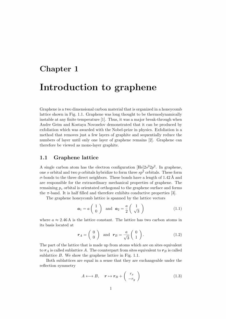
Introduction to graphene
Graphene is a two dimensional carbon material that is organized in a honeycomblattice shown in Fig. 1.1. Graphene was long thought to be thermodynamicallyinstable at any finite temperature [1]. Thus, it was a major break-through whenAndre Geim and Kostaya Novoselov demonstrated that it can be produced byexfoliation which was awarded with the Nobel-prize in physics. Exfoliation is amethod that removes just a few layers of graphite and sequentially reduce thenumbers of layer until only one layer of graphene remains [2]. Graphene cantherefore be viewed as mono-layer graphite.
1.1 Graphene lattice
A single carbon atom has the electron configuration [He]2s22p2. In graphene,one s orbital and two p orbitals hybridize to form three sp2 orbitals. These formσ-bonds to the three direct neighbors. These bonds have a length of 1.42�A andare responsible for the extraordinary mechanical properties of graphene. Theremaining pz orbital is orientated orthogonal to the graphene surface and formsthe π-band. It is half filled and therefore exhibits conductive properties [3].
The graphene honeycomb lattice is spanned by the lattice vectors
a1 = a
(10
)and a2 =
a
2
(1√3
)(1.1)
where a ≈ 2.46�A is the lattice constant. The lattice has two carbon atoms inits basis located at
rA =
(00
)and rB =
a√3
(01
). (1.2)
The part of the lattice that is made up from atoms which are on sites equivalentto rA is called sublattice A. The counterpart from sites equivalent to rB is calledsublattice B. We show the graphene lattice in Fig. 1.1.
Both sublattices are equal in a sense that they are exchangeable under thereflection symmetry
A←→ B, r 7→ rB +
(rx−ry
)(1.3)
1
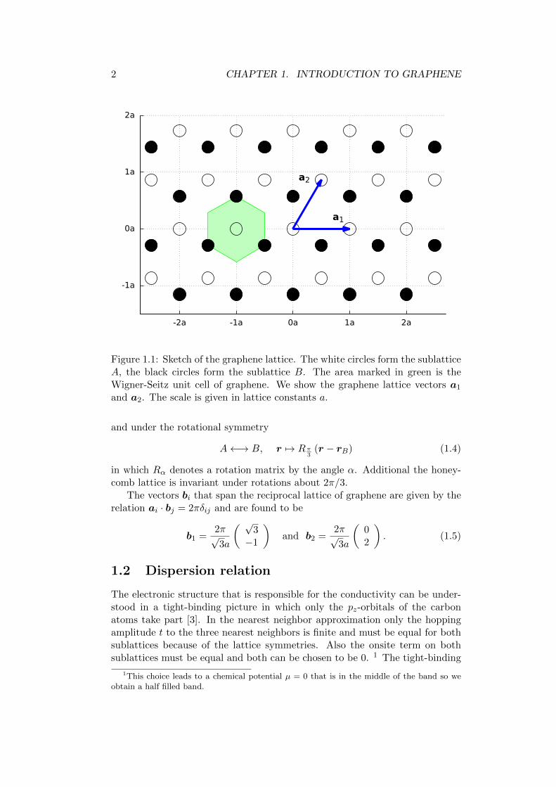
2 CHAPTER 1. INTRODUCTION TO GRAPHENE
-1a
0a
1a
2a
-2a -1a 0a 1a 2a
a1
a2
Figure 1.1: Sketch of the graphene lattice. The white circles form the sublatticeA, the black circles form the sublattice B. The area marked in green is theWigner-Seitz unit cell of graphene. We show the graphene lattice vectors a1and a2. The scale is given in lattice constants a.
and under the rotational symmetry
A←→ B, r 7→ Rπ3
(r − rB) (1.4)
in which Rα denotes a rotation matrix by the angle α. Additional the honey-comb lattice is invariant under rotations about 2π/3.
The vectors bi that span the reciprocal lattice of graphene are given by therelation ai · bj = 2πδij and are found to be
b1 =2π√3a
( √3−1
)and b2 =
2π√3a
(02
). (1.5)
1.2 Dispersion relation
The electronic structure that is responsible for the conductivity can be under-stood in a tight-binding picture in which only the pz-orbitals of the carbonatoms take part [3]. In the nearest neighbor approximation only the hoppingamplitude t to the three nearest neighbors is finite and must be equal for bothsublattices because of the lattice symmetries. Also the onsite term on bothsublattices must be equal and both can be chosen to be 0. 1 The tight-binding
1This choice leads to a chemical potential µ = 0 that is in the middle of the band so weobtain a half filled band.
1.2. DISPERSION RELATION 3
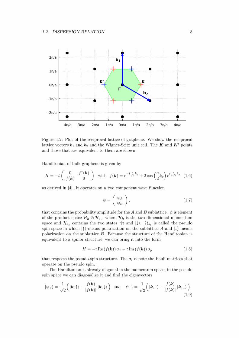
-2π/a
-1π/a
0π/a
1π/a
2π/a
-4π/a -3π/a -2π/a -1π/a 0π/a 1π/a 2π/a 3π/a 4π/a
b2
b1
Γ
KK'
Figure 1.2: Plot of the reciprocal lattice of graphene. We show the reciprocallattice vectors b1 and b2 and the Wigner-Seitz unit cell. The K and K′ pointsand those that are equivalent to them are shown.
Hamiltonian of bulk graphene is given by
H = −t(
0 f∗(k)f(k) 0
)with f(k) = e
−i a√3ky + 2 cos
(a2kx
)ei a2√3ky (1.6)
as derived in [4]. It operates on a two component wave function
ψ =
(ψAψB
), (1.7)
that contains the probability amplitude for the A and B sublattice. ψ is elementof the product space Hk ⊗ Hsz , where Hk is the two dimensional momentumspace and Hsz contains the two states |↑〉 and |↓〉. Hsz is called the pseudospin space in which |↑〉 means polarization on the sublattice A and |↓〉 meanspolarization on the sublattice B. Because the structure of the Hamiltonian isequivalent to a spinor structure, we can bring it into the form
H = −tRe (f(k))σx − t Im (f(k))σy (1.8)
that respects the pseudo-spin structure. The σi denote the Pauli matrices thatoperate on the pseudo spin.
The Hamiltonian is already diagonal in the momentum space, in the pseudospin space we can diagonalize it and find the eigenvectors
|ψ+〉 =1√2
(|k, ↑〉+
f(k)
|f(k)||k, ↓〉
)and |ψ−〉 =
1√2
(|k, ↑〉 − f(k)
|f(k)||k, ↓〉
)(1.9)
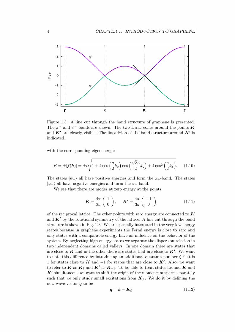
4 CHAPTER 1. INTRODUCTION TO GRAPHENE
-3
-2
-1
0
1
2
3
Γ K K' Γ
π+
π-
E /
t
Figure 1.3: A line cut through the band structure of graphene is presented.The π+ and π− bands are shown. The two Dirac cones around the points Kand K′ are clearly visible. The linearizion of the band structure around K′ isindicated.
with the corresponding eigenenergies
E = ±|f(k)| = ±t
√1 + 4 cos
(a2kx
)cos(√3a
2ky
)+ 4 cos2
(a2kx
). (1.10)
The states |ψ+〉 all have positive energies and form the π+-band. The states|ψ−〉 all have negative energies and form the π−-band.
We see that there are modes at zero energy at the points
K =4π
3a
(10
), K′ =
4π
3a
(−10
)(1.11)
of the reciprocal lattice. The other points with zero energy are connected to Kand K′ by the rotational symmetry of the lattice. A line cut through the bandstructure is shown in Fig. 1.3. We are specially interested in the very low energystates because in graphene experiments the Fermi energy is close to zero andonly states with a comparable energy have an influence on the behavior of thesystem. By neglecting high energy states we separate the dispersion relation intwo independent domains called valleys. In one domain there are states thatare close to K and in the other there are states that are close to K′. We wantto note this difference by introducing an additional quantum number ξ that is1 for states close to K and −1 for states that are close to K′. Also, we wantto refer to K as K1 and K′ as K−1. To be able to treat states around K andK′ simultaneous we want to shift the origin of the momentum space separatelysuch that we only study small excitations from K±. We do it by defining thenew wave vector q to be
q = k −Kξ (1.12)
1.2. DISPERSION RELATION 5
and denote these states as
|q, ξ, sz〉 ∈ Hq ⊗Hξ ⊗Hsz (1.13)
where Hξ is the valley space that contains the states |ξ = ±1〉 and Hq is thenew momentum space with shifted origin.
Because we now study only small excitation from the Dirac points Kξ, wecan expand the Hamiltonian around q = 0 which yields
Hξ = −Re(q · ∇f(k)|k=Kξ
)σx − Im
(q · ∇f(k)|k=Kξ
)σy
=√32 ta(ξqxσx + qyσy).
(1.14)
The eigenstates of the expanded Hamiltonian are
|ψ+, ξ〉 = 1√2
(|k, ξ, ↑〉+
ξqx+iqy|q| |k, ξ, ↓〉
),
|ψ−, ξ〉 = 1√2
(|k, ξ, ↑〉 − ξqx+iqy
|q| |k, ξ, ↓〉) (1.15)
with the corresponding eigenvalues
E(q) = ±√
3
2ta|q|. (1.16)
We found a linear energy-momentum relation, that is called a Dirac cone.In a next step we combine the two Hamiltonians in order to treat the two
valley configurations simultaneous. The complete Hamiltonian with both Diraccones in matrix notation has the form
H =
√3
2ta
(qxσx + qyσy 0
0 −qxσx + qyσy
)(1.17)
and operates on a wave function
ψ =
(ψξ=1
ψξ=−1
)(1.18)
in which both components have the form of the wave function in Eq. (1.7).By performing the unitary transformation
H → HD = UHU †, ψ → ψD = Uψ, U =
(σ0 00 σy
)(1.19)
we yield the Hamiltonian
HD =
√3
2atq · σ idξ (1.20)
that acts as the identity operation idξ on the valley degree of freedom. It isimportant to note that by transforming the Hamiltonian into the form of a DiracHamiltonian, we can only stick to the sublattice polarization interpretation of|↑〉 and |↓〉 as long as we have a complete valley degeneracy.
6 CHAPTER 1. INTRODUCTION TO GRAPHENE
The linear energy-momentum relation we obtained implies a velocity
vf =
√3
2~at (1.21)
that is called the Fermi velocity and can experimentally be found to be vf ≈10× 106 m s−1. It corresponds to t ≈ 2.8 eV. We can now define the momentump = ~q and give the Hamiltonian for bulk graphene
H = vfp · σ. (1.22)
We imply the identity operation on the valley-space when we use it.
1.3 Classical motion
To understand the behavior of graphene under the influence of a magnetic field,we first study the classical behavior of the electrons in graphene. The quantummechanically derived Hamiltonian implies the classical Hamiltonian H = vf |p|.For this problem we can solve the Hamiltonian equations of motions
∂H
∂xi=
dpidt
and∂H
∂pi= −dxi
dt. (1.23)
To implement the magnetic field we have to perform the minimal couplingsubstitution
p 7→ p+ eA (1.24)
for a particle of charge −e where A is the vector potential of the applied mag-netic field such that B = ∇ × A. The vector potential is gauge invariant,therefore we can choose a gauge that is appropriate. For our problem we choosethe Landau gauge
A = −Byex. (1.25)
It respects the invariance of the problem under translations along the x-axiswhich makes the calculations easier. By performing the substitution we obtainthe Hamiltonian
H = vf
√(px −Bey)2 + p2y. (1.26)
The Hamiltonian is neither dependent on the time nor is it dependent onthe coordinate x. Therefore, the energy E = H and the canonic momentum pxare constants of motion. We start with solving for the motion in the y-space
∂H
∂py=v2fHpy =
dy
dt,
∂H
∂y=Bev2fH
(Bey − px) = −dpydt
(1.27)
and see that the motion forms a harmonic oscillator for the momenta py
d2pydt2
= −B2e2v2fH
dy
dt= −
B2e2v4fH2
py. (1.28)
The general solution of Eq. (1.28) assumes the form
py = C sin (ωct+ ϕ0) (1.29)
1.4. LANDAU LEVELS 7
with the integration constants C and ϕ0. The resonance frequency ωc =Bev2f/E is called the cyclotron frequency. Finally, we derive the motion ofy from py
y = − H
B2e2v2f
dpydt
+1
Bepx = − C
Becos (ωct+ ϕ0) +
1
Bepx. (1.30)
The next step is to solve for the motion of x
∂H
∂px=v2fH
(px −Bey) = Cv2fE
cos (ωct+ ϕ0) =dx
dt. (1.31)
We can solve the differential equation by integration and find
x = x0 +C
Besin (ωct+ ϕ0) (1.32)
where x0 is arbitrary. The obtained motion is a circle of radius rc = C/Bearound the position x = x0 and y = px/Be. Because both coordinates arearbitrary values, the center of the circle can be located anywhere.
We can now solve for the energy E of the system by evaluating the Hamil-tonian
H = vf |A| = E. (1.33)
The energy of the electron determines the radius rc = |A|/Be = E/vfBe andthereby completely fixes the motion. rc is called the cyclotron radius. It is themost important characteristic of the classical motion.
1.4 Landau levels
We can also consider the problem by the means of quantum mechanics. To ob-tain the Hamiltonian for electrons in graphene under the influence of a magneticfield we take the Hamiltonian from Eq. (1.22) and again perform the minimalcoupling substitution in the Landau gauge as in Eq. (1.25) which yields theHamiltonian
H = vf (p+ eA)σ = vf (px −Bey)σx + vfpyσy. (1.34)
The Hamiltonian contains the Pauli matrices σ. Because Pauli matrices havethe property
[Ai, Aj ] = 0 =⇒ (A · σ)2 = A2, (1.35)
it is more easy to deal with H2 that is given by
H2 = v2f((px −Bey)2 + p2y
)+v2f [pxσx(pyσy −Bexσy) + (pyσy −Bexσy)pxσx]
= v2f((px −Bey)2 + p2y + σz~Be
).
(1.36)
By squaring the Hamiltonian states which have the same absolute value ofenergy become degenerated.
8 CHAPTER 1. INTRODUCTION TO GRAPHENE
The Hamiltonian commutes with the generator of the translation symmetryin x-direction, therefore the solution in the x-space can be chosen to be planewaves 〈x|kx〉 = exp(ikxx). To solve the equation we can decompose the productspace |ψ〉 = |x〉 ⊗ |y〉 ⊗ |sz〉 and find the Hamiltonian to be
H2 |ψ〉 =[v2f (~kx −Bey)2 + v2fp
2y +Be~sz
]|kx〉 ⊗ |ψy〉 ⊗ |sz〉 . (1.37)
The part of the Hamiltonian that operates in the y-space has the form of aharmonic oscillator with shifted origin by ~kx/Be. We can shift
y → y′ = y − ~kxBe
(1.38)
to bring the problem in the well known harmonic oscillator form
H2 = (vfBey′)2 + (vfpy)
2 +Be~sz = Hosc +Be~sz (1.39)
with an additional energy correction depending on the sublattice degree offreedom. It resembles a harmonic oscillator Hosc that only operates in they-space with the mass m = 1/2v2f and the resonance frequency ω = 2Bev2f .
The eigenvalues of Hosc can be obtained by defining the ladder operators
a =
√Be
2~y′ + i
1√2Be~
py, a† =
√Be
2~y′ − i 1√
2Be~py (1.40)
and identifying Hosc = ~ω(a†a+ 1/2). The problem has the known solutions
Hosc |n〉 = εn |n〉 = ~ω(n+1
2) |n〉 = v2fBe~(2n+ 1) |n〉 with n ∈ N0. (1.41)
In the full H2 the eigenstates of Hosc are also dependent on kx because of theshift in y, we denote them as |n, kx〉. We can now give the full eigenvaluedecomposition
H2 |kx〉 ⊗ |n, kx〉 ⊗ |sz〉 = v2fBe~(2n+ 1 + sz) |kx〉 ⊗ |n, kx〉 ⊗ |sz〉 . (1.42)
Because sz = ±1, we can find one state with E2 = 0 and two states forevery E2 = 2v2fBe~n with n not equal zero. The energy levels E = vf
√2Be~n
are called Landau levels. Because we treated the valley degeneracy implicitly,each of these states is again two times degenerated.
We squared the Hamiltonian, so the eigenstates with the same absolutevalue of energy became degenerate. We want to disentangle the states to getan idea of the sublattice polarization. To do that, we decompose py and y′ intoa and a† in the Hamiltonian from Eq. (1.34) as suggested by [3]. Then, theproblem has the form
H = vf
√Be~
2
[−(a† + a)σx + i(a† − a)σy
]. (1.43)
The states that became degenerate for H2 are |kx, n, ↑〉 and |kx, n+ 1, ↓〉. Tofind the linear combination that forms the eigenstates to the eigenvalues E and
1.4. LANDAU LEVELS 9
−E we evaluate H |kx, n, sz〉. We use that the ladder operator satisfy the rela-tions a |kx, n, sz〉 =
√n |kx, n− 1, sz〉 and a† |kx, n, sz〉 =
√n+ 1 |kx, n+ 1, sz〉
to findH |kx, n, ↑〉 = −vf
√2Be~(n+ 1) |kx, n+ 1, ↓〉 ,
H |kx, n+ 1, ↓〉 = −vf√
2Be~(n+ 1) |kx, n, ↑〉 .(1.44)
The eigenstates of the problem have again the structure known from the freestates
|ψ+〉 = 1√2(|kx, n+ 1, ↓〉+ |kx, n, ↑〉),
|ψ−〉 = 1√2(|kx, n+ 1, ↓〉 − |kx, n, ↑〉)
(1.45)
in which both sublattices are equally occupied.

10 CHAPTER 1. INTRODUCTION TO GRAPHENE
Chapter 2
Simulation methods
The aim of this thesis is to understand the properties of transport through aring shaped graphene device. Because the problem is to complex to be treatedanalytically, we need some tools to study certain properties.
2.1 Tight-binding simulation
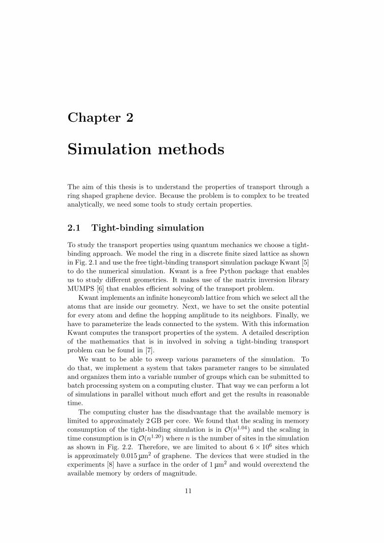
To study the transport properties using quantum mechanics we choose a tight-binding approach. We model the ring in a discrete finite sized lattice as shownin Fig. 2.1 and use the free tight-binding transport simulation package Kwant [5]to do the numerical simulation. Kwant is a free Python package that enablesus to study different geometries. It makes use of the matrix inversion libraryMUMPS [6] that enables efficient solving of the transport problem.
Kwant implements an infinite honeycomb lattice from which we select all theatoms that are inside our geometry. Next, we have to set the onsite potentialfor every atom and define the hopping amplitude to its neighbors. Finally, wehave to parameterize the leads connected to the system. With this informationKwant computes the transport properties of the system. A detailed descriptionof the mathematics that is in involved in solving a tight-binding transportproblem can be found in [7].
We want to be able to sweep various parameters of the simulation. Todo that, we implement a system that takes parameter ranges to be simulatedand organizes them into a variable number of groups which can be submitted tobatch processing system on a computing cluster. That way we can perform a lotof simulations in parallel without much effort and get the results in reasonabletime.
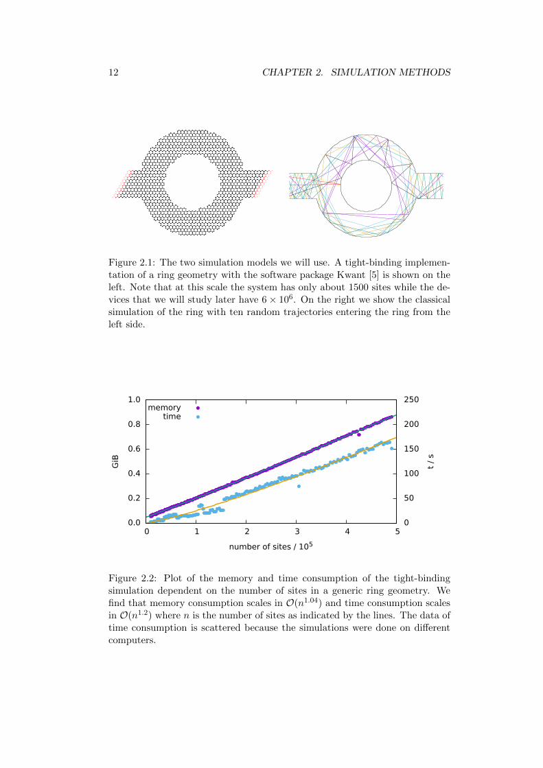
The computing cluster has the disadvantage that the available memory islimited to approximately 2 GB per core. We found that the scaling in memoryconsumption of the tight-binding simulation is in O(n1.04) and the scaling intime consumption is in O(n1.20) where n is the number of sites in the simulationas shown in Fig. 2.2. Therefore, we are limited to about 6× 10⁶ sites whichis approximately 0.015 µm2 of graphene. The devices that were studied in theexperiments [8] have a surface in the order of 1 µm2 and would overextend theavailable memory by orders of magnitude.
11
12 CHAPTER 2. SIMULATION METHODS
Figure 2.1: The two simulation models we will use. A tight-binding implemen-tation of a ring geometry with the software package Kwant [5] is shown on theleft. Note that at this scale the system has only about 1500 sites while the de-vices that we will study later have 6× 10⁶. On the right we show the classicalsimulation of the ring with ten random trajectories entering the ring from theleft side.
0.0
0.2
0.4
0.6
0.8
1.0
0 1 2 3 4 5 0
50
100
150
200
250
GiB
t /
s
number of sites / 105
memorytime
Figure 2.2: Plot of the memory and time consumption of the tight-bindingsimulation dependent on the number of sites in a generic ring geometry. Wefind that memory consumption scales in O(n1.04) and time consumption scalesin O(n1.2) where n is the number of sites as indicated by the lines. The data oftime consumption is scattered because the simulations were done on differentcomputers.
2.2. TRACING OF THE CLASSICAL TRAJECTORIES 13
To deal with this problem we want to study the properties of the DiracHamiltonian
H = vfpσ (2.1)
under the scaling transformation
x 7→ x = sx (2.2)
where s is the scaling. As suggested by [7].Quantum mechanics require that x and p satisfy the canonical commutator
relation[xi, pj ] = [sxi, pj ] = i~δi,j . (2.3)
We see that we can choose p = p/s. Accordingly, the Hamiltonian of the systemtransforms as
H = vf pσ =H
s. (2.4)
It implies that we have to scale up the energy as we scale down the system.We want to study the system under the influence of a magnetic field. We
already discussed this problem in bulk graphene in section 1.4. To perform acorrect scaling of the system we require that the energy quantization we foundstill holds in the scaled system. So we can conclude from
H2 |kx, n, sz〉 = v2f Be~(2n+ 1 + sz) |kx, n, sz〉 (2.5)
that the magnetic field should scale according to
B =B
s2. (2.6)
To get a good picture of the reality the scaling in the energy and the mag-netic field in the simulation have limits. By increasing the energy we get closerto the nonlinear regime of dispersion relation of graphene, that was neglected bylinearizing the problem. By increasing the magnetic field we move toward thetransport regime known as Hofstadter’s butterfly that shows transport charac-teristics that are different from the low magnet field regime. To dodge theseeffects we have to take care that lB � a and H � t.
2.2 Tracing of the classical trajectories
We want to study the ring in the many mode regime, therefore it is probablethat the ring will show some characteristics that can be understood by classicalphysics. To be able to compare the quantum mechanical simulations with theclassical expectations we implement a toolkit in Python to simulate the classicaltransport of electrons through geometrical defined boundaries such as a ring.The classical description of the problem has the advantage that the dependencyof the energy and the magnetic field can be expressed in the single quantitycyclotron radius rc.
We implement the basic set of lines, rays, segments, arcs, and circles tomodel different geometric boundaries and procedures to calculate intersections
14 CHAPTER 2. SIMULATION METHODS
between the boundary and the trajectory of the electron. We want to studysystems that consist of leads through which an electron can enter to a barrierregion. In this region it gets scattered and exits the geometry through the sameor a different lead. Such as a ring shown in Fig. 2.1. To decide if the trajectoryof an electron passes the constriction we trace the trajectory of the electron byrepeatedly calculating the next intersection of the path with the boundary ofthe barrier region and then reflecting it back by using that the angle of reflectionis equal to the angle of incidence. Because our initial implementation in Pythonhad a very bad performance, we ported the code to Cython and optimized ituntil we were able to compute 250 trajectories through a ring per second. Someexample trajectories are shown in Fig. 2.1.
To get the transmission we start the trajectory of the electron in a lead thatconnects to the barrier region. The lead is orientated along the x-axis. Westart at a fixed x-point in the lead. Next, we randomly pick a y-position anda direction to start the trace. We check if this choice of initial conditions ispropagating in the direction of the barrier. Otherwise we discard it and pick anew position and direction. This is necessary because once we apply a magneticfield a trajectory that initially moves away from the device can be brought intothe other direction by the magnetic force. Once we picked a trajectory thatpropagates, we construct the path through the obstacle to check through whichlead it exits.
We will repeat this for many different random initial condition and thancompute the transmission t via
t =T
n(2.7)
where T is the number of transmitted electrons and n is the number of checkedtrajectories. The process is a Bernoulli process because the electron either getsreflected or transmitted. Therefore, T will be binomially distributed and wecan give the variance to be
σ2T = npT (1− pT ) (2.8)
where pT is the actual transmission probability. The resulting uncertainty inthe transmission is given by
σt =
√σ2T
n=
√pT (1− pT )
n. (2.9)
We will typically calculate 105 trajectories. If we assume a transmission prob-ability pT = 0.5 we will have a uncertainty σt ≈ 1.5 · 10−3.
Chapter 3
Nanoribbons and theconnection to the ring
It is important to understand how a straight nanoribbon of graphene behavesbecause every current in and out of a geometry must be carried through somesort of lead that forms a nanoribbon. Before studying the behavior of a fullgraphene ring, we therefore want to concentrate on the connection to the ring.
3.1 Zig-zag and armchair
If we perform a tight-binding simulation of a lead we need to define one unitcell of the lead that is repeated over and over to infinity. This repetition mustbe compatible with the graphene lattice and the direction of the lead musttherefore be a linear combination of the lattice vectors of graphene with integercoefficients.
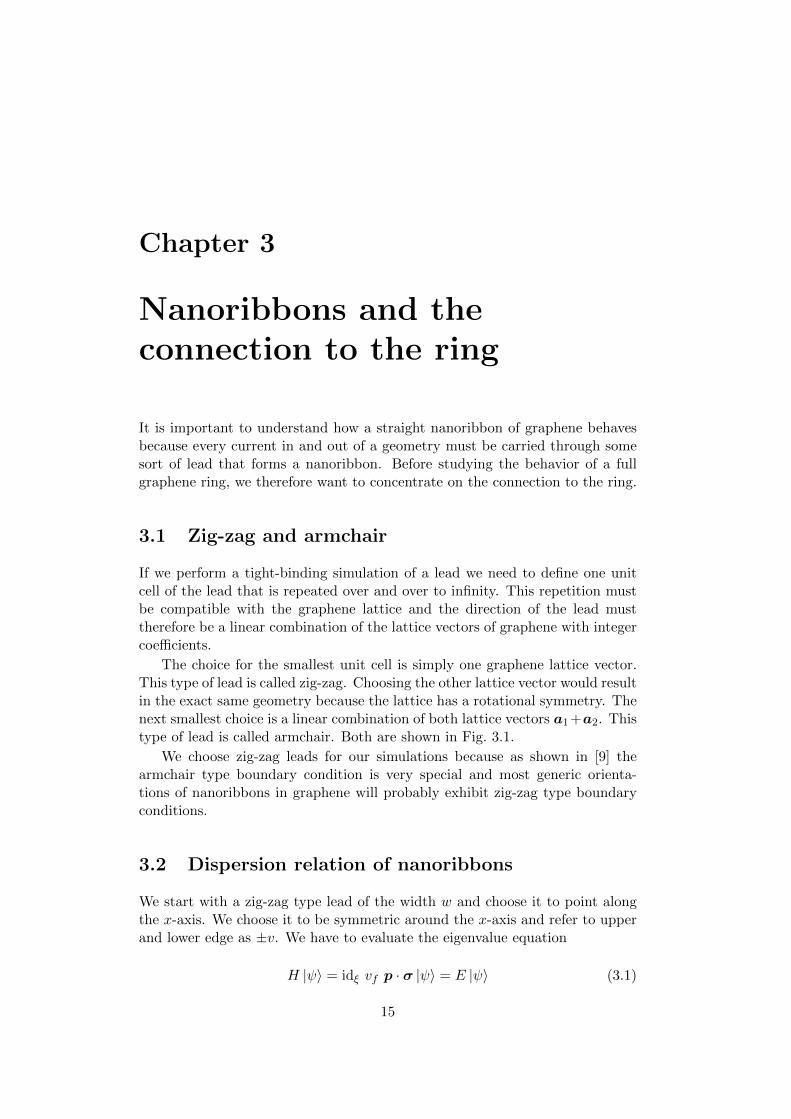
The choice for the smallest unit cell is simply one graphene lattice vector.This type of lead is called zig-zag. Choosing the other lattice vector would resultin the exact same geometry because the lattice has a rotational symmetry. Thenext smallest choice is a linear combination of both lattice vectors a1+a2. Thistype of lead is called armchair. Both are shown in Fig. 3.1.
We choose zig-zag leads for our simulations because as shown in [9] thearmchair type boundary condition is very special and most generic orienta-tions of nanoribbons in graphene will probably exhibit zig-zag type boundaryconditions.
3.2 Dispersion relation of nanoribbons
We start with a zig-zag type lead of the width w and choose it to point alongthe x-axis. We choose it to be symmetric around the x-axis and refer to upperand lower edge as ±v. We have to evaluate the eigenvalue equation
H |ψ〉 = idξ vf p · σ |ψ〉 = E |ψ〉 (3.1)
15
16 CHAPTER 3. CONNECTION TO THE RING
Figure 3.1: The two most simple forms of leads made of graphene. We show azig-zag type nanoribbon on the left and an armchair type on the right. The areasmarked in green are the unit cells of the lead. We show the translation vectorand for the armchair type nanoribbon the decomposition into the graphenelattice vectors. Note that the lattice is rotated in between the two types ofnanoribbons.
that describes the motion of electrons in graphene under the termination con-dition
〈±v, y, ξ, sz| τz ⊗ σz |ψ〉 = ±〈±v, y, ξ, sz| τz ⊗ σz |ψ〉 (3.2)
derived in [9] where τi denote the Pauli matrices on the valley space.To study the eigenenergies of this Hamiltonian we can square it to get rid
of the Pauli matrices. We obtain
H2 = v2f(p2x + p2y
). (3.3)
We see that this Hamiltonian together with the boundary condition is trans-lational invariant in the x-direction. Therefore, we can reduce the problem toone dimension by using the wave solution
〈x|kx〉 = eikxx, H2 |ψ〉 = idx ⊗H2y |kx〉 ⊗ |ψy〉 , H2
y = v2f(~2k2x + p2y
)(3.4)
in the x-space. The eigenvalue problem can now be formulated as the differentialequation
E2 〈y, ξ, sz|ψy〉 = v2f (~2k2x − ~2∂2y) 〈y, ξ, sz|ψy〉 (3.5)
in the y-space. We can rewrite the problem as
− (k2f − k2x) 〈y, ξ, sz|ψy〉 = ∂2y 〈y, ξ, sz|ψy〉 (3.6)
where kf = E/vf~ is the Fermi wavevector. We want to use k2y as a shortnotation for k2f − k2x.
The solution of the problem is derived in [3]. They find that the termina-tion conditions allow both real and imaginary solutions for ky. The imaginarysolutions are relevant for edge states that are of importance in the few moderegime as we are interested in the many mode regime only the quantization forreal ky
kx =ky
tan(wky)(3.7)
3.3. THE INFLUENCE OF A MAGNETIC FIELD 17
-0.01
0
0.01
0.02
0.03
0.04
0.05
0.06
0.07
0.08
0.09
2 2.05 2.1 2.15
E /
t
ky a
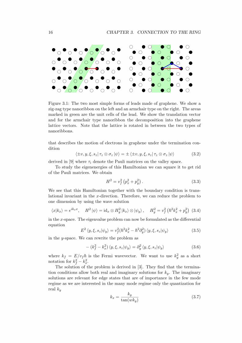
Figure 3.2: The analytic calculation (lines) and the tight-binding simulation(dots) of the dispersion relation of a zig-zag type nanoribbon with width w =400a around the K point is shown. The offset in the momentum is given bythe location of the Dirac point at 2π/3a. The part of the simulation that is notcovered by the analytic calculation are edge states. We only show states withpositive energy.
is of interest to us. The conductivity of nanoribbon at a certain energy E isquantized and given by the number of modes that propagate times the con-ductance quantum G0 = 2e2/h. The quantization condition in Eq (3.7) impliesthat a new mode is added to the dispersion relation whenever tan(wkf ) is diver-gent. We can conclude that a change in the conductivity will occur wheneverwkf = (n+ 1/2)π.
We performed a tight-binding simulation of a graphene nanoribbon withzig-zag type boundary conditions and compare the results with the analyticallyfound solution as shown in Fig. 3.2.
3.3 The influence of a magnetic field
Now we want to study the behavior of an ideal lead under the influence of amagnetic field. The free solution with no boundary conditions in bulk graphenewas done in section 1.4. Since we did not brake the translational symmetry thatwas used in the derivation of the Hamiltonian in Eq. (1.36), we can solve it withrespect to the confining hard wall. Because we want to apply a semi-classicalsolution, we bring the problem into the position space representation
〈y, kx, sz|ψ〉 = ψsz ,kx(y),v2f((~kx +Bey)2 − ~2∂2y +Be~sz
)ψsz ,kx(y) = E2ψsz ,kx(y).
(3.8)
18 CHAPTER 3. CONNECTION TO THE RING
We rearrange the equation in a way that the differentiation stands withoutprefactor. In the form((
kx +Be
~y
)2
+Be
~sz − ∂2y
)ψsz ,kx(y) =
E2
v2f~2ψsz ,kx(y) (3.9)
we can identify a new important length scale in the description of the problem.It is given by Be/~ = l−2B where lB is the magnetic length. The magnetic lengthis defined to be the radius of a circle through which one magnetic flux quantumφ0 = e/h flows. Additionally, we can identify the Fermi wave vector kf andconclude ((
kx +y
l2B
)2
+szl2B− ∂2y
)ψsz ,kx(y) = k2fψsz ,kx(y). (3.10)
This differential equation has a form that can be approximated using the semi-classical approach∫ a
b
√(kx +
y
l2B
)2
− k2f ∓1
l2Bdy′ = π(n+ γ) with n ∈ N0 (3.11)
where γ is the Maslov index of the problem. We can simplify the integrationby the substitutions
y′ = y + kxl2B ε± = k2f ±
1
l2B(3.12)
so that we obtain
1
l2B
∫ a
b
√y′2 − ε±l4B dy′ =
l2Bε±2
sin−1(
y′
l2B√ε±
)+y′
2
√ε± −
y′2
l4B
∣∣∣∣∣b
a
. (3.13)
The integration has a nice geometric interpretation: it measures the area ofthe overlap from the lead and the circle that a free electron in bulk materialwould describe [10]. The interpretation is shown in Fig. 3.3. By multiplyingwith l−2B it gives π times the number of magnetic flux quanta that flows throughthis area. We can find the cyclotron radius rc from the classical discussion ofelectrons in graphene under the influence of a magnetic field in
√ε± l
2B, but with
an additional correction due to the setting of the pseudo spin sz, that was notpart of the classical discussion.
To evaluate the definite integration we have to fix the integration limits aand b. At this point, we have to make a case distinction and decide whetherthe classic return point is given by the hard wall or the magnetic field. We findthe limits to be
a = min(√ε± l
2B, v − kxl2B
)=
{ √ε± l
2B, if
√ε± <
vl2B− kx,
v − kxl2B, otherwise,
b = max(−√ε± l2B,−v − kxl2B
)=
{−√ε± l2B, if
√ε± <
vl2B
+ kx,
−v − kxl2B, otherwise.
(3.14)
3.3. THE INFLUENCE OF A MAGNETIC FIELD 19
A B C
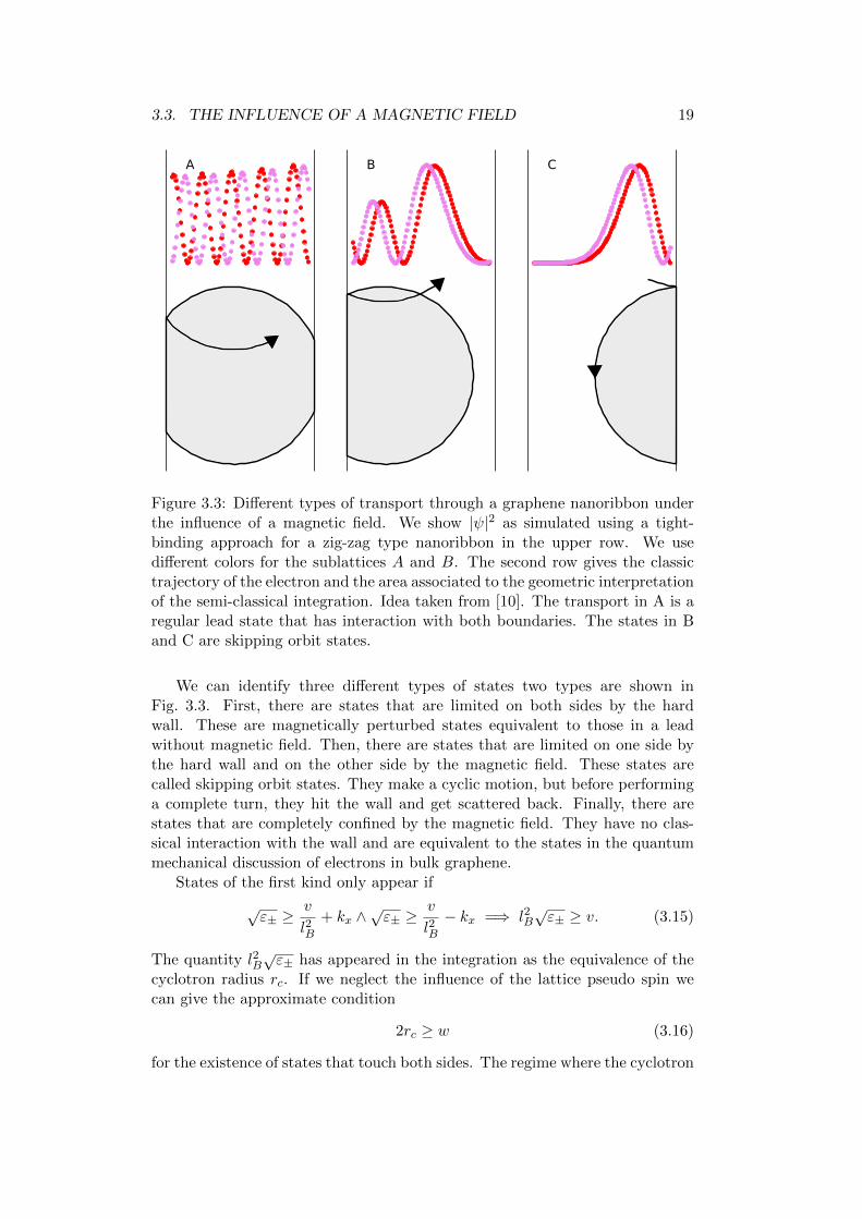
Figure 3.3: Different types of transport through a graphene nanoribbon underthe influence of a magnetic field. We show |ψ|2 as simulated using a tight-binding approach for a zig-zag type nanoribbon in the upper row. We usedifferent colors for the sublattices A and B. The second row gives the classictrajectory of the electron and the area associated to the geometric interpretationof the semi-classical integration. Idea taken from [10]. The transport in A is aregular lead state that has interaction with both boundaries. The states in Band C are skipping orbit states.
We can identify three different types of states two types are shown inFig. 3.3. First, there are states that are limited on both sides by the hardwall. These are magnetically perturbed states equivalent to those in a leadwithout magnetic field. Then, there are states that are limited on one side bythe hard wall and on the other side by the magnetic field. These states arecalled skipping orbit states. They make a cyclic motion, but before performinga complete turn, they hit the wall and get scattered back. Finally, there arestates that are completely confined by the magnetic field. They have no clas-sical interaction with the wall and are equivalent to the states in the quantummechanical discussion of electrons in bulk graphene.
States of the first kind only appear if
√ε± ≥
v
l2B+ kx ∧
√ε± ≥
v
l2B− kx =⇒ l2B
√ε± ≥ v. (3.15)
The quantity l2B√ε± has appeared in the integration as the equivalence of the
cyclotron radius rc. If we neglect the influence of the lattice pseudo spin wecan give the approximate condition
2rc ≥ w (3.16)
for the existence of states that touch both sides. The regime where the cyclotron
20 CHAPTER 3. CONNECTION TO THE RING
10
E /
t
B / T
3.1
3.3
3.5
3.7
3.9
10 30 50 70 9010
50
G /
G0
A
B / T
tight-bindingapprox.
20
30
40
10 30 50 70 90
B
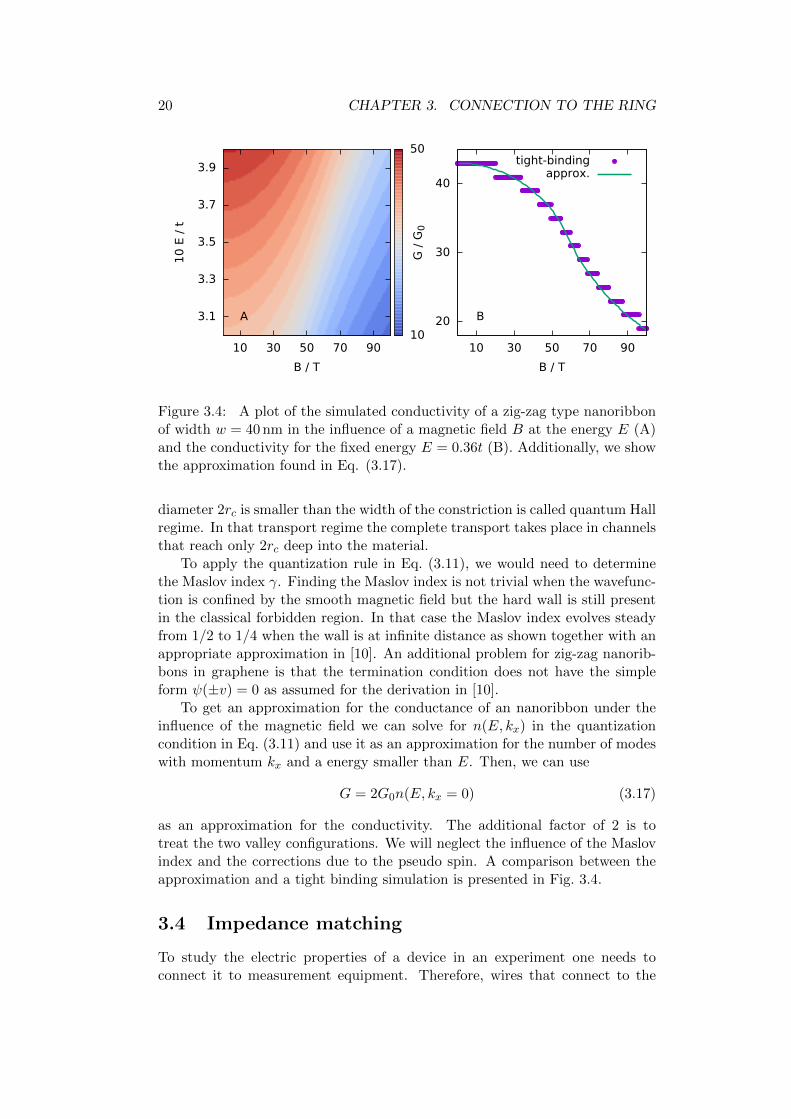
Figure 3.4: A plot of the simulated conductivity of a zig-zag type nanoribbonof width w = 40 nm in the influence of a magnetic field B at the energy E (A)and the conductivity for the fixed energy E = 0.36t (B). Additionally, we showthe approximation found in Eq. (3.17).
diameter 2rc is smaller than the width of the constriction is called quantum Hallregime. In that transport regime the complete transport takes place in channelsthat reach only 2rc deep into the material.
To apply the quantization rule in Eq. (3.11), we would need to determinethe Maslov index γ. Finding the Maslov index is not trivial when the wavefunc-tion is confined by the smooth magnetic field but the hard wall is still presentin the classical forbidden region. In that case the Maslov index evolves steadyfrom 1/2 to 1/4 when the wall is at infinite distance as shown together with anappropriate approximation in [10]. An additional problem for zig-zag nanorib-bons in graphene is that the termination condition does not have the simpleform ψ(±v) = 0 as assumed for the derivation in [10].
To get an approximation for the conductance of an nanoribbon under theinfluence of the magnetic field we can solve for n(E, kx) in the quantizationcondition in Eq. (3.11) and use it as an approximation for the number of modeswith momentum kx and a energy smaller than E. Then, we can use
G = 2G0n(E, kx = 0) (3.17)
as an approximation for the conductivity. The additional factor of 2 is totreat the two valley configurations. We will neglect the influence of the Maslovindex and the corrections due to the pseudo spin. A comparison between theapproximation and a tight binding simulation is presented in Fig. 3.4.
3.4 Impedance matching
To study the electric properties of a device in an experiment one needs toconnect it to measurement equipment. Therefore, wires that connect to the
3.4. IMPEDANCE MATCHING 21
35
37
39
41
43
45
47
49
0.3 0.32 0.34 0.36 0.38 0.4
A
Gf/
fG0
Ef/ft
transmissionconductivity
0
0.5
1
1.5
2
0.3 0.32 0.34 0.36 0.38 0.4
B
n
Ef/ft
reflection
C
Edope E
lmatch
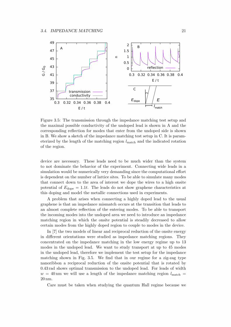
Figure 3.5: The transmission through the impedance matching test setup andthe maximal possible conductivity of the undoped lead is shown in A and thecorresponding reflection for modes that enter from the undoped side is shownin B. We show a sketch of the impedance matching test setup in C. It is param-eterized by the length of the matching region lmatch and the indicated rotationof the region.
device are necessary. These leads need to be much wider than the systemto not dominate the behavior of the experiment. Connecting wide leads in asimulation would be numerically very demanding since the computational effortis dependent on the number of lattice sites. To be able to simulate many modesthat connect down to the area of interest we dope the wires to a high onsitepotential of Edope = 1.1t. The leads do not show graphene characteristics atthis doping and model the metallic connections used in experiments.
A problem that arises when connecting a highly doped lead to the usualgraphene is that an impedance mismatch occurs at the transition that leads toan almost complete reflection of the entering modes. To be able to transportthe incoming modes into the undoped area we need to introduce an impedancematching region in which the onsite potential is steadily decreased to allowcertain modes from the highly doped region to couple to modes in the device.
In [7] the two models of linear and reciprocal reduction of the onsite energyin different orientations were studied as impedance matching regions. Theyconcentrated on the impedance matching in the low energy regime up to 13modes in the undoped lead. We want to study transport at up to 45 modesin the undoped lead, therefore we implement the test setup for the impedancematching shown in Fig. 3.5. We find that in our regime for a zig-zag typenanoribbon a reciprocal reduction of the onsite potential that is rotated by0.43 rad shows optimal transmission to the undoped lead. For leads of widthw = 40 nm we will use a length of the impedance matching region lmatch =20 nm.
Care must be taken when studying the quantum Hall regime because we
22 CHAPTER 3. CONNECTION TO THE RING
found that in the doped area modes that would normally be protected by thestrong magnetic fields and the small cyclotron radius can interact with eachother. For this reason, we must not use the impedance matching when studyingeffects that are related to quantum Hall channels.
3.5 T-Junction
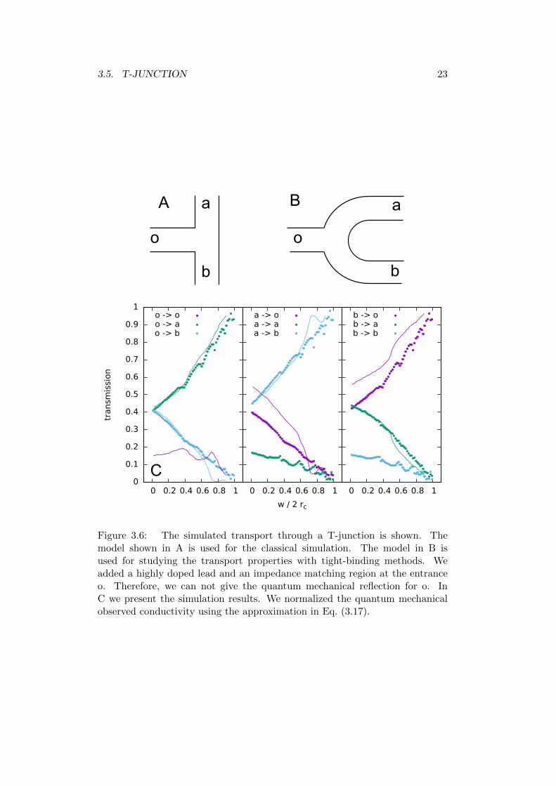
To get an insight in the way the electrons enter the ring we first study thetransport through a T-junction. We model the geometry of a T-junction withtight-binding methods and perform a transport simulation dependent on theapplied magnetic field. Because it is not trivial to implement connections toa system that point in different directions, we also implement half of the ring.A sketch of the setup is shown in Fig. 3.6. We also implemented a classicaltransport simulation for a T-junction. Both results can be found in Fig. 3.6.
We can now compare the classical transmission with the quantum mechan-ical transmission. We find that in both cases the applied magnetic field breaksthe symmetry of the two arms a and b and creates one arm through which thetransport happens favorably. The major difference between the quantum me-chanical and the classical description is the fact that in the classical simulationthere is no backscattering when entering the T-junction through the arm a orb.
3.5. T-JUNCTION 23
0
0.1
0.2
0.3
0.4
0.5
0.6
0.7
0.8
0.9
1
0 0.2 0.4 0.6 0.8 1
transm
issi
on
o -> oo -> ao -> b
0 0.2 0.4 0.6 0.8 1
w / 2 rc
a -> oa -> aa -> b
0 0.2 0.4 0.6 0.8 1
b -> ob -> ab -> b
A Ba
b
o o
a
b
C
Figure 3.6: The simulated transport through a T-junction is shown. Themodel shown in A is used for the classical simulation. The model in B isused for studying the transport properties with tight-binding methods. Weadded a highly doped lead and an impedance matching region at the entranceo. Therefore, we can not give the quantum mechanical reflection for o. InC we present the simulation results. We normalized the quantum mechanicalobserved conductivity using the approximation in Eq. (3.17).

24 CHAPTER 3. CONNECTION TO THE RING
Chapter 4
Transport through a graphenering
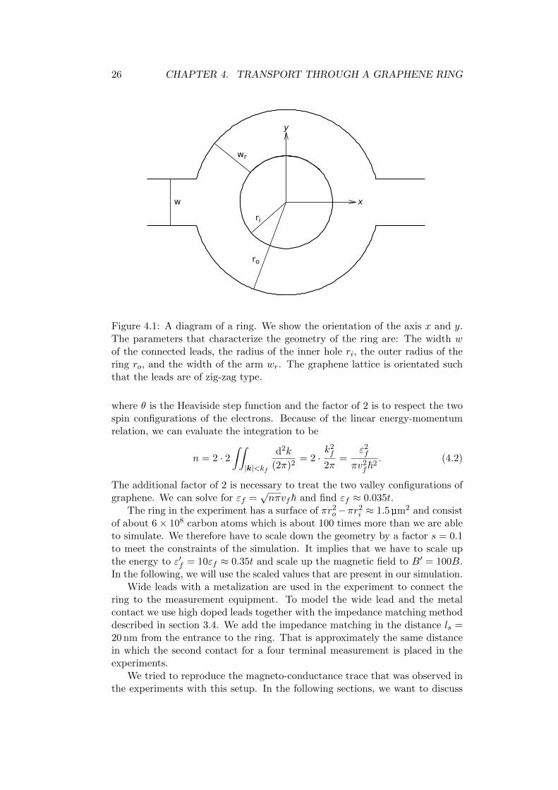
Finally, we want to study a ring made of graphene. First, we want to definethe way we talk about the geometry. The ring is parameterized by the innerradius ri, the outer radius ro, the width w of the leads that connect to the ring,and the width of the arm of the ring wr. We want to orientate our coordinatesystem such that the connecting lead points along the x-axis and orientate thegraphene lattice in the tight-binding such that the leads that connect to thesystem are of zig-zag type. The setup is shown in Fig. 4.1.
4.1 Experimental data and the parameter for thesimulation
The aim of this thesis is to theoretically understand certain properties that wereobserved by [8]. They have achieved to fabricate graphene rings in very highquality using graphene that is encapsulated between two sheets of hexagonalboron nitride. These sandwiches are known to have high electron mobilities andtherefore will exhibit properties close to pure graphene. The geometry that wasstudied has an inner radius ri = 400 nm, an outer radius ro = 800 nm, and awidth w = 400 nm. Its electrical properties were measured at temperatures aslow as 36 mK and in magnetic fields up to 8 T.
To perform our simulations we need to determine the Fermi energy εf ofthe system because that will give us the energy E with respect to the Diraccone at which we perform the simulation. In the experiment the parameterthat controls the Fermi energy is the backgate voltage VBG. A voltage thatis applied at the back of the device and affects the charge carrier density n.At a backgate voltage of −15 V a charge carrier density of 7.6× 1011 cm−2 wasfound [8].
The charge carrier density n is given by the integration about the densityof states to the Fermi energy
n = 2
∫∫d2k
(2π)2θ[E(k)− εf ] (4.1)
25
26 CHAPTER 4. TRANSPORT THROUGH A GRAPHENE RING
x
y
ri
ro
w
wr
Figure 4.1: A diagram of a ring. We show the orientation of the axis x and y.The parameters that characterize the geometry of the ring are: The width wof the connected leads, the radius of the inner hole ri, the outer radius of thering ro, and the width of the arm wr. The graphene lattice is orientated suchthat the leads are of zig-zag type.
where θ is the Heaviside step function and the factor of 2 is to respect the twospin configurations of the electrons. Because of the linear energy-momentumrelation, we can evaluate the integration to be
n = 2 · 2∫∫|k|<kf
d2k
(2π)2= 2 ·
k2f2π
=ε2f
πv2f~2. (4.2)
The additional factor of 2 is necessary to treat the two valley configurations ofgraphene. We can solve for εf =
√nπvf~ and find εf ≈ 0.035t.
The ring in the experiment has a surface of πr2o−πr2i ≈ 1.5 µm2 and consistof about 6× 10⁸ carbon atoms which is about 100 times more than we are ableto simulate. We therefore have to scale down the geometry by a factor s = 0.1to meet the constraints of the simulation. It implies that we have to scale upthe energy to ε′f = 10εf ≈ 0.35t and scale up the magnetic field to B′ = 100B.In the following, we will use the scaled values that are present in our simulation.
Wide leads with a metalization are used in the experiment to connect thering to the measurement equipment. To model the wide lead and the metalcontact we use high doped leads together with the impedance matching methoddescribed in section 3.4. We add the impedance matching in the distance ls =20 nm from the entrance to the ring. That is approximately the same distancein which the second contact for a four terminal measurement is placed in theexperiments.
We tried to reproduce the magneto-conductance trace that was observed inthe experiments with this setup. In the following sections, we want to discuss
4.2. INCREASE OF CONDUCTIVITY 27
20
25
30
35A
G /
G0
simulation
0.0 0.1 0.2 0.3 0.4 0.5 0.6 0.7 0.8
B
G [
arb
. unit
s]
B / T
experimental data
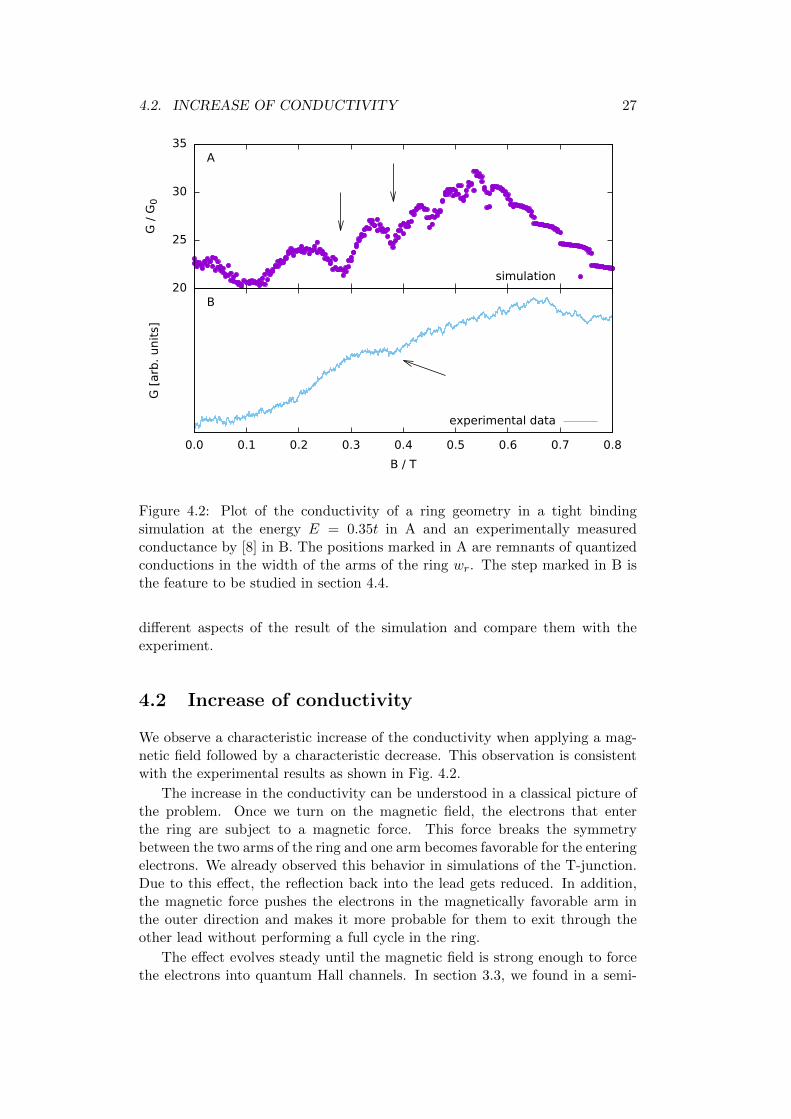
Figure 4.2: Plot of the conductivity of a ring geometry in a tight bindingsimulation at the energy E = 0.35t in A and an experimentally measuredconductance by [8] in B. The positions marked in A are remnants of quantizedconductions in the width of the arms of the ring wr. The step marked in B isthe feature to be studied in section 4.4.
different aspects of the result of the simulation and compare them with theexperiment.
4.2 Increase of conductivity
We observe a characteristic increase of the conductivity when applying a mag-netic field followed by a characteristic decrease. This observation is consistentwith the experimental results as shown in Fig. 4.2.
The increase in the conductivity can be understood in a classical picture ofthe problem. Once we turn on the magnetic field, the electrons that enterthe ring are subject to a magnetic force. This force breaks the symmetrybetween the two arms of the ring and one arm becomes favorable for the enteringelectrons. We already observed this behavior in simulations of the T-junction.Due to this effect, the reflection back into the lead gets reduced. In addition,the magnetic force pushes the electrons in the magnetically favorable arm inthe outer direction and makes it more probable for them to exit through theother lead without performing a full cycle in the ring.
The effect evolves steady until the magnetic field is strong enough to forcethe electrons into quantum Hall channels. In section 3.3, we found in a semi-
28 CHAPTER 4. TRANSPORT THROUGH A GRAPHENE RING
10
E /
t
B / T
3.1
3.3
3.5
3.7
3.9
0.1 0.3 0.5 0.7 0.910
20
30
40
G /
G0
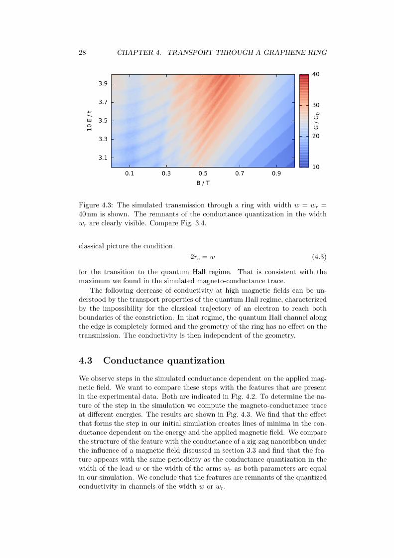
Figure 4.3: The simulated transmission through a ring with width w = wr =40 nm is shown. The remnants of the conductance quantization in the widthwr are clearly visible. Compare Fig. 3.4.
classical picture the condition
2rc = w (4.3)
for the transition to the quantum Hall regime. That is consistent with themaximum we found in the simulated magneto-conductance trace.
The following decrease of conductivity at high magnetic fields can be un-derstood by the transport properties of the quantum Hall regime, characterizedby the impossibility for the classical trajectory of an electron to reach bothboundaries of the constriction. In that regime, the quantum Hall channel alongthe edge is completely formed and the geometry of the ring has no effect on thetransmission. The conductivity is then independent of the geometry.
4.3 Conductance quantization
We observe steps in the simulated conductance dependent on the applied mag-netic field. We want to compare these steps with the features that are presentin the experimental data. Both are indicated in Fig. 4.2. To determine the na-ture of the step in the simulation we compute the magneto-conductance traceat different energies. The results are shown in Fig. 4.3. We find that the effectthat forms the step in our initial simulation creates lines of minima in the con-ductance dependent on the energy and the applied magnetic field. We comparethe structure of the feature with the conductance of a zig-zag nanoribbon underthe influence of a magnetic field discussed in section 3.3 and find that the fea-ture appears with the same periodicity as the conductance quantization in thewidth of the lead w or the width of the arms wr as both parameters are equalin our simulation. We conclude that the features are remnants of the quantizedconductivity in channels of the width w or wr.
4.4. SIGNATURES OF BALLISTIC TRANSPORT 29
10
E /
t
B / T
3.1
3.3
3.5
3.7
3.9
0.1 0.3 0.5 0.7
A
B / T
0.1 0.3 0.5 0.710
30
G /
G0
B
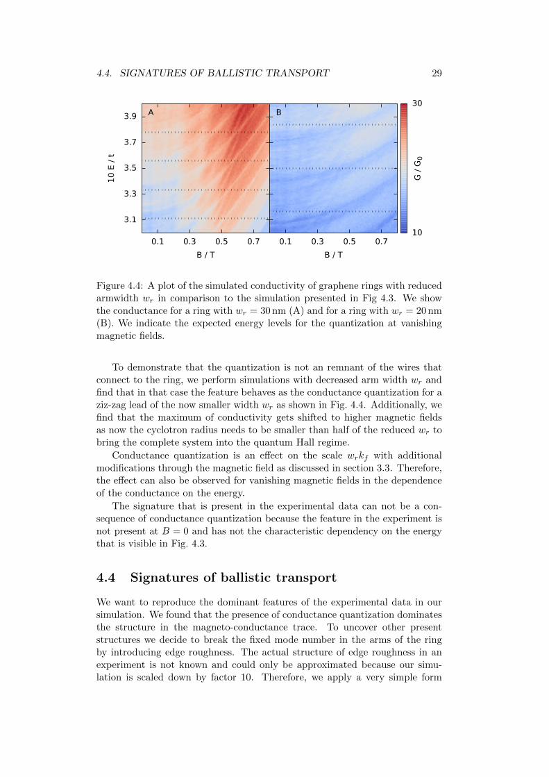
Figure 4.4: A plot of the simulated conductivity of graphene rings with reducedarmwidth wr in comparison to the simulation presented in Fig 4.3. We showthe conductance for a ring with wr = 30 nm (A) and for a ring with wr = 20 nm(B). We indicate the expected energy levels for the quantization at vanishingmagnetic fields.
To demonstrate that the quantization is not an remnant of the wires thatconnect to the ring, we perform simulations with decreased arm width wr andfind that in that case the feature behaves as the conductance quantization for aziz-zag lead of the now smaller width wr as shown in Fig. 4.4. Additionally, wefind that the maximum of conductivity gets shifted to higher magnetic fieldsas now the cyclotron radius needs to be smaller than half of the reduced wr tobring the complete system into the quantum Hall regime.
Conductance quantization is an effect on the scale wrkf with additionalmodifications through the magnetic field as discussed in section 3.3. Therefore,the effect can also be observed for vanishing magnetic fields in the dependenceof the conductance on the energy.
The signature that is present in the experimental data can not be a con-sequence of conductance quantization because the feature in the experiment isnot present at B = 0 and has not the characteristic dependency on the energythat is visible in Fig. 4.3.
4.4 Signatures of ballistic transport
We want to reproduce the dominant features of the experimental data in oursimulation. We found that the presence of conductance quantization dominatesthe structure in the magneto-conductance trace. To uncover other presentstructures we decide to break the fixed mode number in the arms of the ringby introducing edge roughness. The actual structure of edge roughness in anexperiment is not known and could only be approximated because our simu-lation is scaled down by factor 10. Therefore, we apply a very simple form
30 CHAPTER 4. TRANSPORT THROUGH A GRAPHENE RING
10
E /
t
B / T
3.1
3.3
3.5
3.7
3.9
0.3 0.5 0.710
34
G /
G0
BG
/ G
0
B / T
a = 0nma = 1nma = 2nma = 3nma = 4nma = 5nm
14
34
0.3 0.5 0.7
A
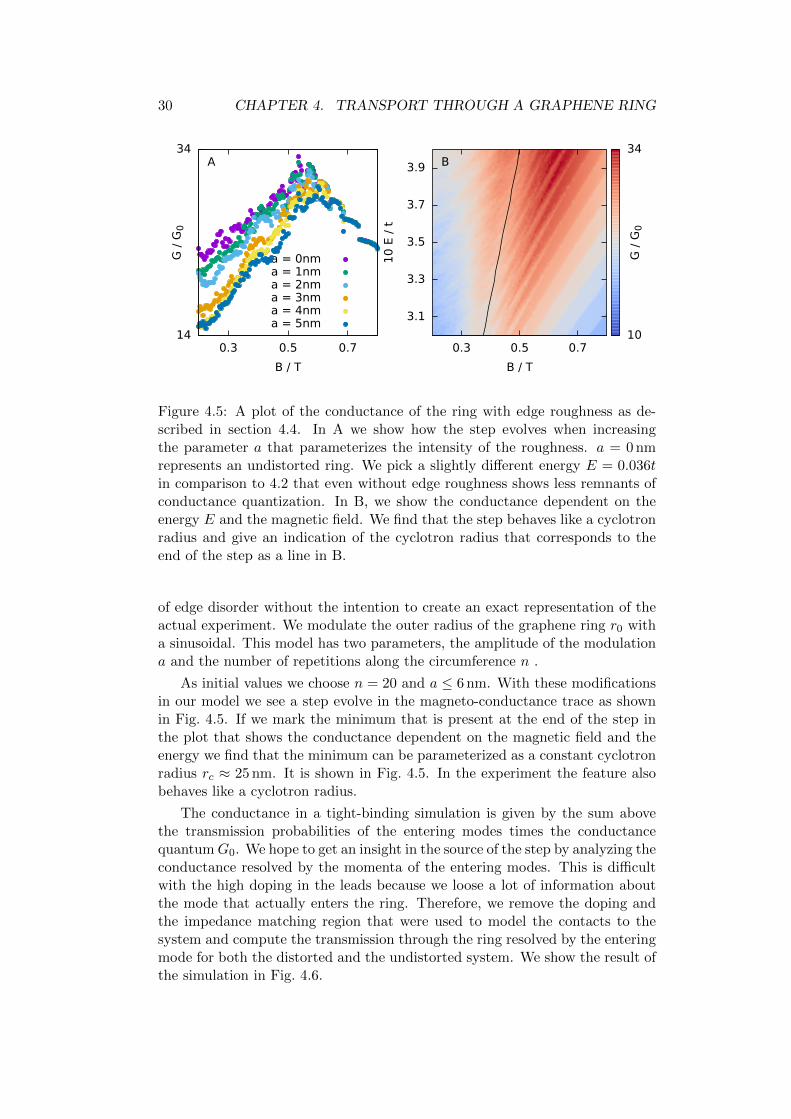
Figure 4.5: A plot of the conductance of the ring with edge roughness as de-scribed in section 4.4. In A we show how the step evolves when increasingthe parameter a that parameterizes the intensity of the roughness. a = 0 nmrepresents an undistorted ring. We pick a slightly different energy E = 0.036tin comparison to 4.2 that even without edge roughness shows less remnants ofconductance quantization. In B, we show the conductance dependent on theenergy E and the magnetic field. We find that the step behaves like a cyclotronradius and give an indication of the cyclotron radius that corresponds to theend of the step as a line in B.
of edge disorder without the intention to create an exact representation of theactual experiment. We modulate the outer radius of the graphene ring r0 witha sinusoidal. This model has two parameters, the amplitude of the modulationa and the number of repetitions along the circumference n .
As initial values we choose n = 20 and a ≤ 6 nm. With these modificationsin our model we see a step evolve in the magneto-conductance trace as shownin Fig. 4.5. If we mark the minimum that is present at the end of the step inthe plot that shows the conductance dependent on the magnetic field and theenergy we find that the minimum can be parameterized as a constant cyclotronradius rc ≈ 25 nm. It is shown in Fig. 4.5. In the experiment the feature alsobehaves like a cyclotron radius.
The conductance in a tight-binding simulation is given by the sum abovethe transmission probabilities of the entering modes times the conductancequantumG0. We hope to get an insight in the source of the step by analyzing theconductance resolved by the momenta of the entering modes. This is difficultwith the high doping in the leads because we loose a lot of information aboutthe mode that actually enters the ring. Therefore, we remove the doping andthe impedance matching region that were used to model the contacts to thesystem and compute the transmission through the ring resolved by the enteringmode for both the distorted and the undistorted system. We show the result ofthe simulation in Fig. 4.6.
4.4. SIGNATURES OF BALLISTIC TRANSPORT 31
0
0.2
0.4
0.6
0.0 0.2 0.5 0.8
B /
T
kx a
A
0.0 0.2 0.5 0.8
kx a
0.1
1.0
Tra
nsm
issi
on
B
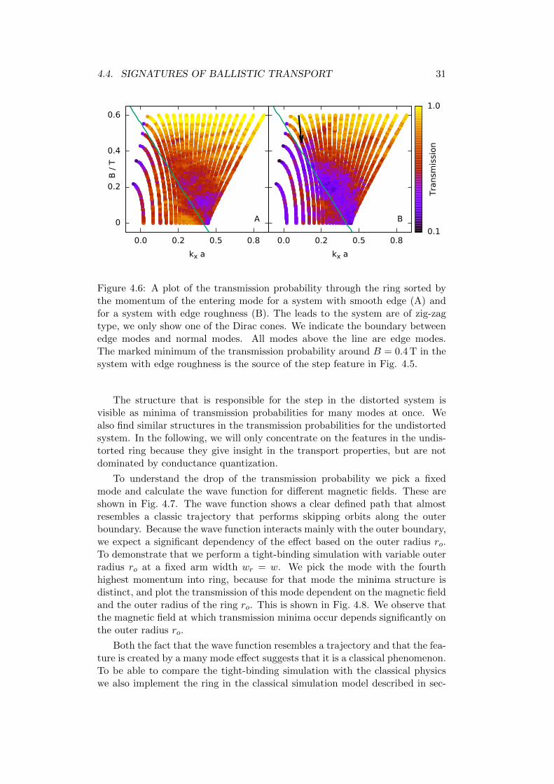
Figure 4.6: A plot of the transmission probability through the ring sorted bythe momentum of the entering mode for a system with smooth edge (A) andfor a system with edge roughness (B). The leads to the system are of zig-zagtype, we only show one of the Dirac cones. We indicate the boundary betweenedge modes and normal modes. All modes above the line are edge modes.The marked minimum of the transmission probability around B = 0.4 T in thesystem with edge roughness is the source of the step feature in Fig. 4.5.
The structure that is responsible for the step in the distorted system isvisible as minima of transmission probabilities for many modes at once. Wealso find similar structures in the transmission probabilities for the undistortedsystem. In the following, we will only concentrate on the features in the undis-torted ring because they give insight in the transport properties, but are notdominated by conductance quantization.
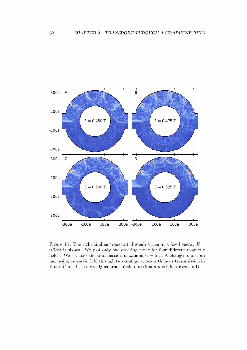
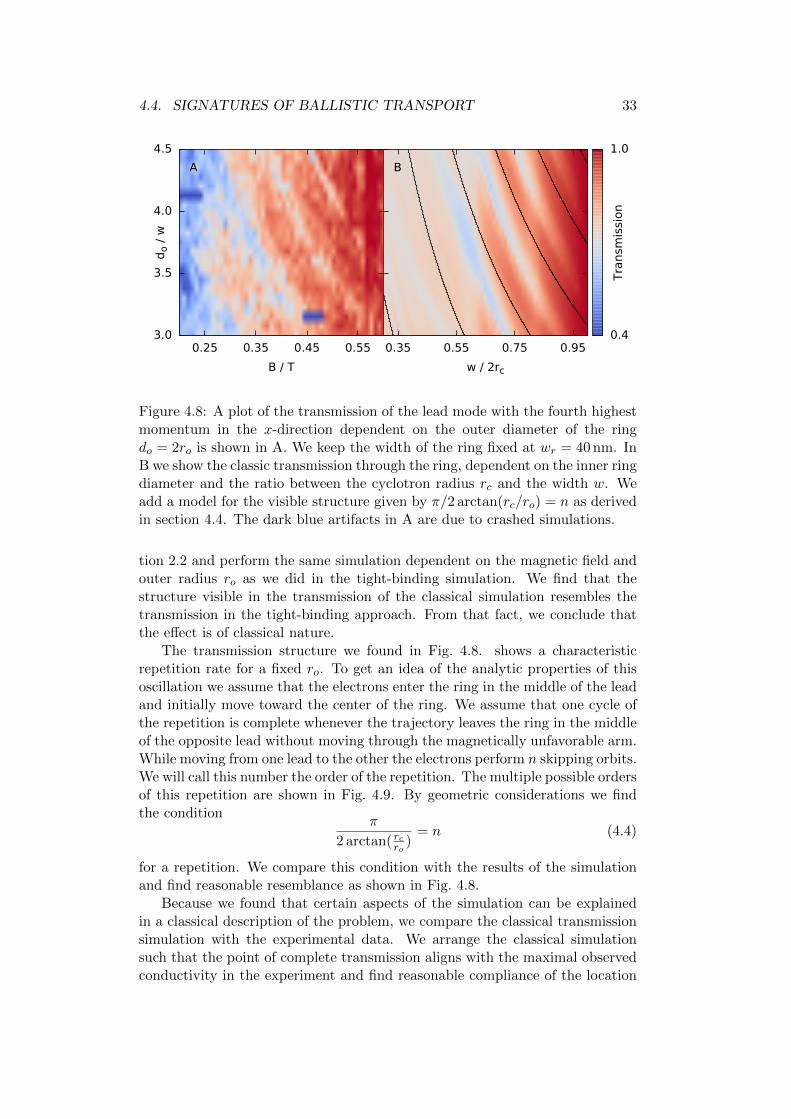
To understand the drop of the transmission probability we pick a fixedmode and calculate the wave function for different magnetic fields. These areshown in Fig. 4.7. The wave function shows a clear defined path that almostresembles a classic trajectory that performs skipping orbits along the outerboundary. Because the wave function interacts mainly with the outer boundary,we expect a significant dependency of the effect based on the outer radius ro.To demonstrate that we perform a tight-binding simulation with variable outerradius ro at a fixed arm width wr = w. We pick the mode with the fourthhighest momentum into ring, because for that mode the minima structure isdistinct, and plot the transmission of this mode dependent on the magnetic fieldand the outer radius of the ring ro. This is shown in Fig. 4.8. We observe thatthe magnetic field at which transmission minima occur depends significantly onthe outer radius ro.
Both the fact that the wave function resembles a trajectory and that the fea-ture is created by a many mode effect suggests that it is a classical phenomenon.To be able to compare the tight-binding simulation with the classical physicswe also implement the ring in the classical simulation model described in sec-
32 CHAPTER 4. TRANSPORT THROUGH A GRAPHENE RING
-300a
-100a
100a
300a
B = 0.450 T
A
B = 0.475 T
B
-300a
-100a
100a
300a
-300a -100a 100a 300a
B = 0.500 T
C
-300a -100a 100a 300a
B = 0.525 T
D
Figure 4.7: The tight-binding transport through a ring at a fixed energy E =0.036t is shown. We plot only one entering mode for four different magneticfields. We see how the transmission maximum n = 5 in A changes under anincreasing magnetic field through two configurations with lower transmission inB and C until the next higher transmission maximum n = 6 is present in D.
4.4. SIGNATURES OF BALLISTIC TRANSPORT 33
do /
w
B / T
3.0
3.5
4.0
4.5
0.25 0.35 0.45 0.55
A
w / 2rc
0.35 0.55 0.75 0.950.4
1.0
Tra
nsm
issi
on
B
Figure 4.8: A plot of the transmission of the lead mode with the fourth highestmomentum in the x-direction dependent on the outer diameter of the ringdo = 2ro is shown in A. We keep the width of the ring fixed at wr = 40 nm. InB we show the classic transmission through the ring, dependent on the inner ringdiameter and the ratio between the cyclotron radius rc and the width w. Weadd a model for the visible structure given by π/2 arctan(rc/ro) = n as derivedin section 4.4. The dark blue artifacts in A are due to crashed simulations.
tion 2.2 and perform the same simulation dependent on the magnetic field andouter radius ro as we did in the tight-binding simulation. We find that thestructure visible in the transmission of the classical simulation resembles thetransmission in the tight-binding approach. From that fact, we conclude thatthe effect is of classical nature.
The transmission structure we found in Fig. 4.8. shows a characteristicrepetition rate for a fixed ro. To get an idea of the analytic properties of thisoscillation we assume that the electrons enter the ring in the middle of the leadand initially move toward the center of the ring. We assume that one cycle ofthe repetition is complete whenever the trajectory leaves the ring in the middleof the opposite lead without moving through the magnetically unfavorable arm.While moving from one lead to the other the electrons perform n skipping orbits.We will call this number the order of the repetition. The multiple possible ordersof this repetition are shown in Fig. 4.9. By geometric considerations we findthe condition
π
2 arctan( rcro )= n (4.4)
for a repetition. We compare this condition with the results of the simulationand find reasonable resemblance as shown in Fig. 4.8.
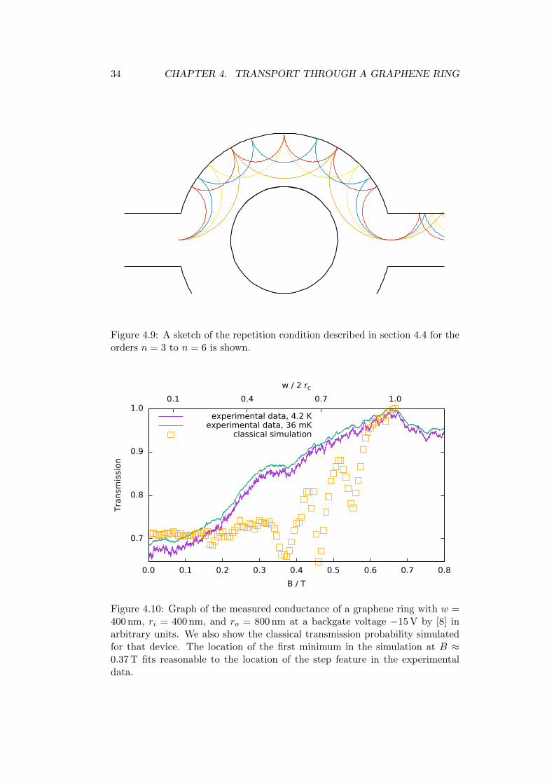
Because we found that certain aspects of the simulation can be explainedin a classical description of the problem, we compare the classical transmissionsimulation with the experimental data. We arrange the classical simulationsuch that the point of complete transmission aligns with the maximal observedconductivity in the experiment and find reasonable compliance of the location
34 CHAPTER 4. TRANSPORT THROUGH A GRAPHENE RING
Figure 4.9: A sketch of the repetition condition described in section 4.4 for theorders n = 3 to n = 6 is shown.
0.7
0.8
0.9
1.0
0.0 0.1 0.2 0.3 0.4 0.5 0.6 0.7 0.8
0.1 0.4 0.7 1.0
Tra
nsm
issi
on
B / T
w / 2 rc
experimental data, 4.2 Kexperimental data, 36 mK
classical simulation
Figure 4.10: Graph of the measured conductance of a graphene ring with w =400 nm, ri = 400 nm, and ro = 800 nm at a backgate voltage −15 V by [8] inarbitrary units. We also show the classical transmission probability simulatedfor that device. The location of the first minimum in the simulation at B ≈0.37 T fits reasonable to the location of the step feature in the experimentaldata.
4.5. AHARONOV-BOHM OSCILLATIONS 35
0.7
0.8
0.9
1.0
0.0 0.1 0.2 0.3 0.4 0.5 0.6
0.1 0.4 0.7 1.0Tra
nsm
issi
on
B / T
w / 2 rc
classictight-binding
Figure 4.11: Plot of the transmission through a circle that can be viewed as aring with inner radius ri = 0, outer radius ro = 80 nm, and width of the leadw = 40 nm. We normalized the tight-binding simulation to the conductivity ofa lead with width w using the approximation in Eq. (3.17). We additionallyshow the classical transmission through the circle.
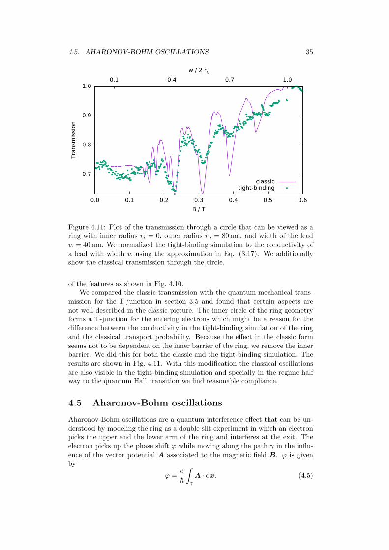
of the features as shown in Fig. 4.10.We compared the classic transmission with the quantum mechanical trans-
mission for the T-junction in section 3.5 and found that certain aspects arenot well described in the classic picture. The inner circle of the ring geometryforms a T-junction for the entering electrons which might be a reason for thedifference between the conductivity in the tight-binding simulation of the ringand the classical transport probability. Because the effect in the classic formseems not to be dependent on the inner barrier of the ring, we remove the innerbarrier. We did this for both the classic and the tight-binding simulation. Theresults are shown in Fig. 4.11. With this modification the classical oscillationsare also visible in the tight-binding simulation and specially in the regime halfway to the quantum Hall transition we find reasonable compliance.
4.5 Aharonov-Bohm oscillations
Aharonov-Bohm oscillations are a quantum interference effect that can be un-derstood by modeling the ring as a double slit experiment in which an electronpicks the upper and the lower arm of the ring and interferes at the exit. Theelectron picks up the phase shift ϕ while moving along the path γ in the influ-ence of the vector potential A associated to the magnetic field B. ϕ is givenby
ϕ =e
~
∫γA · dx. (4.5)
36 CHAPTER 4. TRANSPORT THROUGH A GRAPHENE RING
1
2
3
4
5
6
7
8
9
10
0.00 0.01 0.02 0.03 0.04 0.05
G /
G0
B / T
A
G [
arb
. unit
s]
0.05t0.10t0.15t
B
200 400 600 800
G [
arb
. unit
s]
fB T
0.05t0.10t0.15t
C
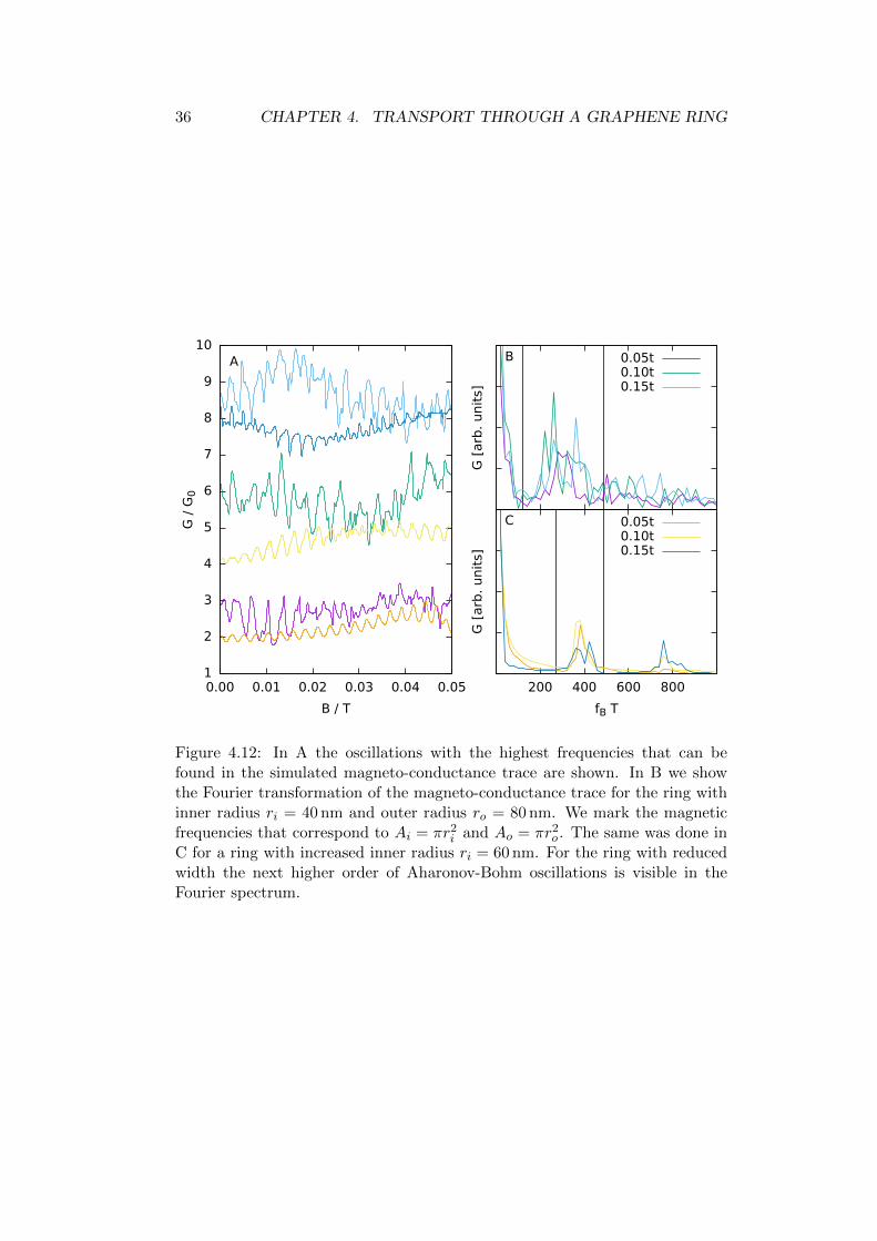
Figure 4.12: In A the oscillations with the highest frequencies that can befound in the simulated magneto-conductance trace are shown. In B we showthe Fourier transformation of the magneto-conductance trace for the ring withinner radius ri = 40 nm and outer radius ro = 80 nm. We mark the magneticfrequencies that correspond to Ai = πr2i and Ao = πr2o . The same was done inC for a ring with increased inner radius ri = 60 nm. For the ring with reducedwidth the next higher order of Aharonov-Bohm oscillations is visible in theFourier spectrum.
4.5. AHARONOV-BOHM OSCILLATIONS 37
To study the interference only the phase difference between the path alongthe upper arm of the ring γ and the path along the lower arm of the ring γ′
is of interest. Calculating the phase difference ∆ϕ along these two paths isequivalent to evaluate the phase picked up when the electron moves along theclosed path C that consist of γ followed by γ′ in reverse. Because we study theconstant magnetic field B, the integration can be solved by Stokes’s theoremto be
∆ϕ =e
~ACB (4.6)
where AC is the area enclosed by C. The area is unique because the problem istwo dimensional. That leads to a magnetic frequency fB = e/2π~AC associatedto the area AC . More on the topic of Aharonov-Bohm oscillations can be foundin [8].
We find oscillations in the simulation that have high frequencies in compar-ison to the other effects discussed before. They are visible for all energies wesimulated. But they do not have a well defined sinusoidal shape. This is alsovisible in the Fourier spectrum of the conductance trace. The oscillations andthe Fourier transformation are shown in Fig. 4.12. We can compute the fre-quencies that are associated with the area of the inner barrier of the ring to be121 T−1 and for the area enclosed by the outer radius of the ring to be 486 T−1.When we mark these frequencies in the Fourier spectrum, we can find that be-tween those frequencies lies a diffuse maximum. Therefore, the oscillations areindeed Aharonov-Bohm oscillations .
We do not obtain a pure oscillation because there is no prominent enclosedarea for the different paths of the electrons. This results in a diffuse wide maxi-mum in the Fourier spectrum. To be able to observer higher quality oscillationswe have to define a clearer path for the electrons that can be done by decreasingthe width wr of the ring. Then the inner barrier becomes more prominent asan area that is enclosed by electron trajectories. To prove it we also performsimulations with an increased inner radius ri = 60 nm that implies a reducedarm width of wr = 20 nm. We are able to observe better defined Aharonov-Bohm oscillations which is also visible in the Fourier spectrum. We now finda peak between the old frequency associated with the outer ring and the newfrequency 273 T−1 that results from the changed inner radius. Now we can alsoidentify contributions of Aharonov-Bohm oscillations in higher order. Theseare contribution by path that lead around the inner barrier multiple times.

38 CHAPTER 4. TRANSPORT THROUGH A GRAPHENE RING
Chapter 5
Summary
In this thesis, we first gave an introduction to the electronic properties of bulkgraphene. Next, we introduced two simulation methods that can be used tostudy certain transport properties. Because we want to understand the trans-port through a ring, we first analyzed the way electrons enter a ring geometryby studying the behavior of nanoribbons and T-junctions. Finally, we studiedthe transport through a complete graphene ring.
We were able to reproduce certain aspects of the data measured by [8]. Atthe beginning of our investigation we gave an insight into the rise followed bya decrease of the conductivity at rising magnetic fields. Then, we studied theeffect of conductance quantization. We argued that this type of modulation isnot present in the experimental data and tried to uncover more of the structureby introducing edge roughness to our model. We found an effect of classicaltransport associated to the geometry of the ring that leads to oscillations inthe magneto-conductance trace. We presented a model for the behavior of thiseffect and were able to reproduce it in a tight-binding simulation. In the end, westudied Aharonov-Bohm oscillations and showed that the purity of the observedoscillations are related to the width of the ring.
39

40 CHAPTER 5. SUMMARY
Bibliography
[1] A. K. Geim and K. S. Novoselov, Nat. Mater. 6, 183 (2007).
[2] K. S. Novoselov, Science 306, 666 (2004).
[3] A. H. C. Neto, F. Guinea, N. M. R. Peres, K. S. Novoselov, and A. K.Geim, Rev. Mod. Phys. 81, 109 (2009).
[4] P. R. Wallace, Phys. Rev. 71, 622 (1947).
[5] C. W. Groth, M. Wimmer, A. R. Akhmerov, and X. Waintal, New J. Phys.16, 063065 (2014).
[6] P. R. Amestoy, I. S. Duff, J.-Y. L'Excellent, and J. Koster, SIAM. J.Matrix Anal. & Appl. 23, 15 (2001).
[7] D. Dresen, Quantum transport of non-interacting electrons in 2d systemsof arbitrary geometries, 2014.
[8] M. Oellers, Aharonov-bohm effect in high-mobility graphene rings, 2015.
[9] A. R. Akhmerov and C. W. J. Beenakker, Phys. Rev. B 77, 085423 (2008).
[10] G. Montambaux, Eur. Phys. J. B 79, 215 (2011).
41


![Oscillations mécaniques libres non amorties Oscillations ...ww2.cnam.fr/physique/PHR004/04_L08_PHR004.pdf · Leçon n°8 : Oscillations [1] PHR 004 1 Oscillations mécaniques libres](https://img.pdfslide.tips/doc/110x75/5b968ab509d3f206218b9064/oscillations-mecaniques-libres-non-amorties-oscillations-ww2cnamfrphysiquephr00404l08.jpg)