Embed Size (px)
Citation preview
R59
A 26.2Mpixel, 74fps, Global Shutter CMOS Imagerwith 20Gb/s Interface for Multi Object Monitoring
Cedric Esquenet1, John Compiet2, Tim Blanchaert3,Tomas Geurts4, Joost Decupere5
ON SemiconductorSchalienhoevedreef 20B, 2800 Mechelen, Belgium
[email protected], [email protected], [email protected],[email protected], [email protected]
Abstract—Current developments in CMOS imagers favourhigher resolutions, increasing pixel rates [1] and on-chip con-figurability. This paper presents a 25.5 mm x 32.5 mm sizedCMOS imager targeted for high-end machine vision industryfeaturing pipelined global shutter. This reconfigurable operatingmode imager is composed of 5120 x 5120 5T pixels with pinnedphotodiodes on 4.5 µm pitch. Up to 32 regions of interest canbe programmed in the sensor. The high level of configurabilityin conjunction with high speed readout enables the possibility tomonitor multiple moving objects.
I. INTRODUCTION
Sixty-four 10 bit A/D converter outputs are multiplexed tothirty-two 10 bit serial LVDS output channels reaching anaggregate datarate of 19.84 Gb/s at 74 frames per secondat full resolution. Higher frame rates can be achieved usingwindowed or 2x2 pixel binned readout modes. The sensorfeatures 128 busses that run over the full width of the chipenabling fast windowing modes. In architectures with columnparallel A/D converters [2], the line rate is fixed, and onlychanging the Y-dimension of the window helps to increasethe frame rate. The benefit of the proposed architecture is thatthe pixel rate is kept constant while it is possible to increasethe frame rate by reducing the Y- and X-dimensions of thewindow.
II. ARCHITECTURE
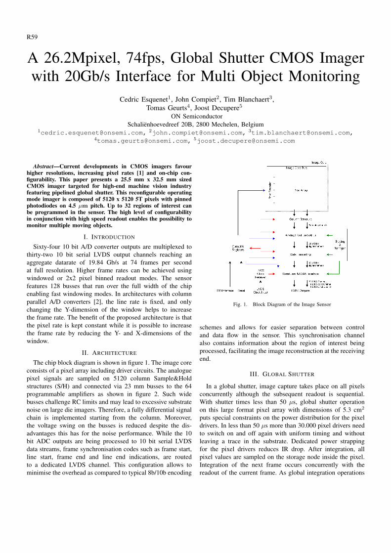
The chip block diagram is shown in figure 1. The image coreconsists of a pixel array including driver circuits. The analoguepixel signals are sampled on 5120 column Sample&Holdstructures (S/H) and connected via 23 mm busses to the 64programmable amplifiers as shown in figure 2. Such widebusses challenge RC limits and may lead to excessive substratenoise on large die imagers. Therefore, a fully differential signalchain is implemented starting from the column. Moreover,the voltage swing on the busses is reduced despite the dis-advantages this has for the noise performance. While the 10bit ADC outputs are being processed to 10 bit serial LVDSdata streams, frame synchronisation codes such as frame start,line start, frame end and line end indications, are routedto a dedicated LVDS channel. This configuration allows tominimise the overhead as compared to typical 8b/10b encoding
Fig. 1. Block Diagram of the Image Sensor
schemes and allows for easier separation between controland data flow in the sensor. This synchronisation channelalso contains information about the region of interest beingprocessed, facilitating the image reconstruction at the receivingend.
III. GLOBAL SHUTTER
In a global shutter, image capture takes place on all pixelsconcurrently although the subsequent readout is sequential.With shutter times less than 50 µs, global shutter operationon this large format pixel array with dimensions of 5.3 cm2
puts special constraints on the power distribution for the pixeldrivers. In less than 50 µs more than 30.000 pixel drivers needto switch on and off again with uniform timing and withoutleaving a trace in the substrate. Dedicated power strappingfor the pixel drivers reduces IR drop. After integration, allpixel values are sampled on the storage node inside the pixel.Integration of the next frame occurs concurrently with thereadout of the current frame. As global integration operations
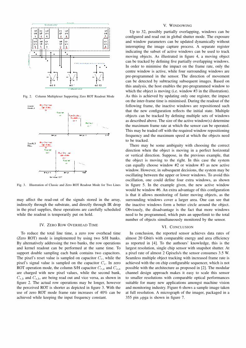
Fig. 2. Column Multiplexer Supporting Zero ROT Readout Mode
Fig. 3. Illustration of Classic and Zero ROT Readout Mode for Two Lines
may affect the read-out of the signals stored in the array,indirectly through the substrate, and directly through IR dropin the pixel supplies, these operations are carefully scheduledwhile the readout is temporarily put on hold.
IV. ZERO ROW OVERHEAD TIME
To reduce the total line time, a zero row overhead time(Zero ROT) mode is implemented by using two S/H banks.By alternatively addressing the two banks, the row operationsand kernel readout can be performed at the same time. Tosupport double sampling each bank contains two capacitors.The pixel’s reset value is sampled on capacitor Cr, while thepixel’s signal value is sampled on the capacitor Cs. In zeroROT operation mode, the column S/H capacitor Cr,a and Cs,a
are charged with new pixel values, while the second bank,Cr,b and Cs,b, are being read out and vice versa, as shown infigure 2. The actual row operations may be longer, howeverthe perceived ROT is shorter as depicted in figure 3. With theuse of zero ROT mode frame rate increases of 40% can beachieved while keeping the input frequency constant.
V. WINDOWING
Up to 32, possibly partially overlapping, windows can beconfigured and read out in global shutter mode. The exposureand window parameters can be updated dynamically withoutinterrupting the image capture process. A separate registerindicating the subset of active windows can be used to trackmoving objects. As illustrated in figure 4, a moving objectcan be tracked by defining five partially overlapping windows.In order to minimise the impact on the frame rate, only thecentre window is active, while four surrounding windows arepre-programmed in the sensor. The direction of movementcan be detected by subtracting subsequent images. Based onthis analysis, the host enables the pre-programmed window towhich the object is moving (i.e. window #3 in the illustration).As this is achieved by updating only one register, the impacton the inter-frame time is minimised. During the readout of thefollowing frame, the inactive windows are repositioned suchthat the new configuration reflects the initial state. Multipleobjects can be tracked by defining multiple sets of windowsas described above. The size of the active window(s) determinethe maximum frame rate at which the sensor can be operated.This may be traded off with the required window repositioningfrequency and the maximum speed at which the objects needto be tracked.
There may be some ambiguity with choosing the correctdirection when the object is moving in a perfect horizontalor vertical direction. Suppose, in the previous example, thatthe object is moving to the right. In this case the systemcan equally choose window #2 or window #3 as new activewindow. However, in subsequent decisions, the system may beoscillating between the upper or lower windows. To avoid thisoscillation, one could define four extra windows, as shownin figure 5. In the example given, the new active windowwould be window #6. An extra advantage of this configurationis that it allows monitoring of faster moving objects, as thesurrounding windows cover a larger area. One can see thatthe inactive windows form a better circle around the object.Obviously, the disadvantage is the fact that more windowsneed to be programmed, which puts an upperlimit to the totalnumber of objects simultaneously monitored by the sensor.
VI. CONCLUSION
In conclusion, the reported sensor achieves data rates ofalmost 20 Gbit/s with comparable energy and area efficiencyas reported in [4]. To the authours’ knowledge, this is thelargest resolution, single chip sensor with snapshot shutter. Ata pixel rate of almost 2 Gpixels/s the sensor consumes 3.5 W.Seamless multiple object tracking with increased frame rate isachieved with the on chip configurable sequencer, which is notpossible with the architecture as proposed in [2]. The modularchannel design approach makes it easy to scale this sensorto smaller resolutions with comparable optical performancessuitable for many new applications amongst machine visionand monitoring industry. Figure 6 shows a sample image takenat full resolution. A micrograph of the imager, packaged in a355 pin µpga is shown in figure 7.
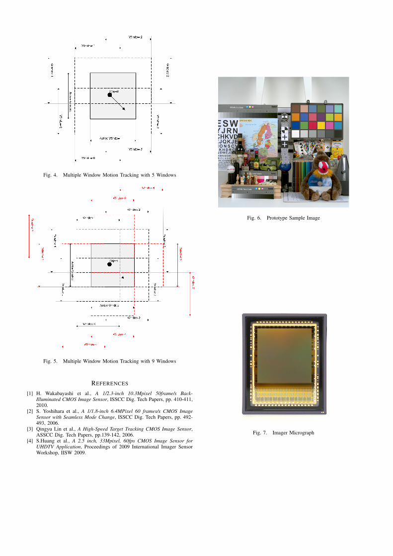
Fig. 4. Multiple Window Motion Tracking with 5 Windows
Fig. 5. Multiple Window Motion Tracking with 9 Windows
REFERENCES
[1] H. Wakabayashi et al., A 1/2.3-inch 10.3Mpixel 50frame/s Back-Illuminated CMOS Image Sensor, ISSCC Dig. Tech Papers, pp. 410-411,2010.
[2] S. Yoshihara et al., A 1/1.8-inch 6.4MPixel 60 frames/s CMOS ImageSensor with Seamless Mode Change, ISSCC Dig. Tech Papers, pp. 492-493, 2006.
[3] Qingyu Lin et al., A High-Speed Target Tracking CMOS Image Sensor,ASSCC Dig. Tech Papers, pp.139-142, 2006.
[4] S.Huang et al., A 2.5 inch, 33Mpixel, 60fps CMOS Image Sensor forUHDTV Application, Proceedings of 2009 International Imager SensorWorkshop, IISW 2009.
Fig. 6. Prototype Sample Image
Fig. 7. Imager Micrograph


![5142116A TILKNYTNING A 1] KOMPATIBILITÄT IZYMO SHUTTER ...€¦ · DA FI NL 5142116A IZYMO SHUTTER RECEIVER io F/CE/NE/SE Ref. : 1822660A INTRODUKTION Mikromodulet IZYMO SHUTTER](https://img.pdfslide.tips/doc/110x75/605b3261ca15db4936229e4a/5142116a-tilknytning-a-1-kompatibilitt-izymo-shutter-da-fi-nl-5142116a-izymo.jpg)