Embed Size (px)
Citation preview
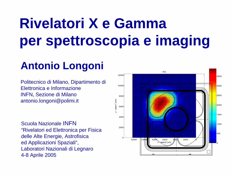
Rivelatori X e Gamma per spettroscopia e imagingAntonio LongoniPolitecnico di Milano, Dipartimento di Elettronica e InformazioneINFN, Sezione di [email protected]
Scuola Nazionale INFN“Rivelatori ed Elettronica per Fisica delle Alte Energie, Astrofisicaed Applicazioni Spaziali“, Laboratori Nazionali di Legnaro4-8 Aprile 2005
Summary
First part•why “low capacitance” for spectroscopic detectors (in other words, why SDDs?): some basic concepts on signal processing
Second part•Introduction to some new SDDs and SDD monolithic arrays•Some applications in material analysis, in biomedicine and in atomic physics
The interaction of the radiation with the detector
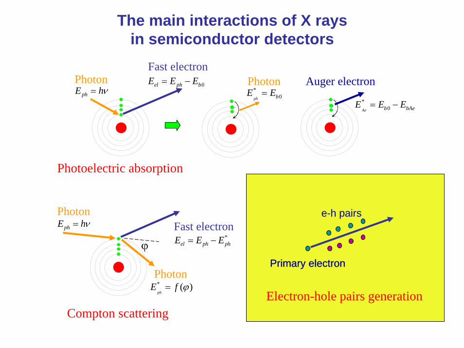
The main interactions of X raysin semiconductor detectors
Fast electron
phE hν=0el ph bE E E= −Photon
*0ph bE E=
Photon Auger electron*
0Ae b bAeE E E= −
Photoelectric absorption
Primary electronPrimary electron
e-h pairs
Electron-hole pairs generation
PhotonphE hν= Fast electron
Photon
ϕ
* ( )ph
E f ϕ=
*el ph phE E E= −
Compton scattering
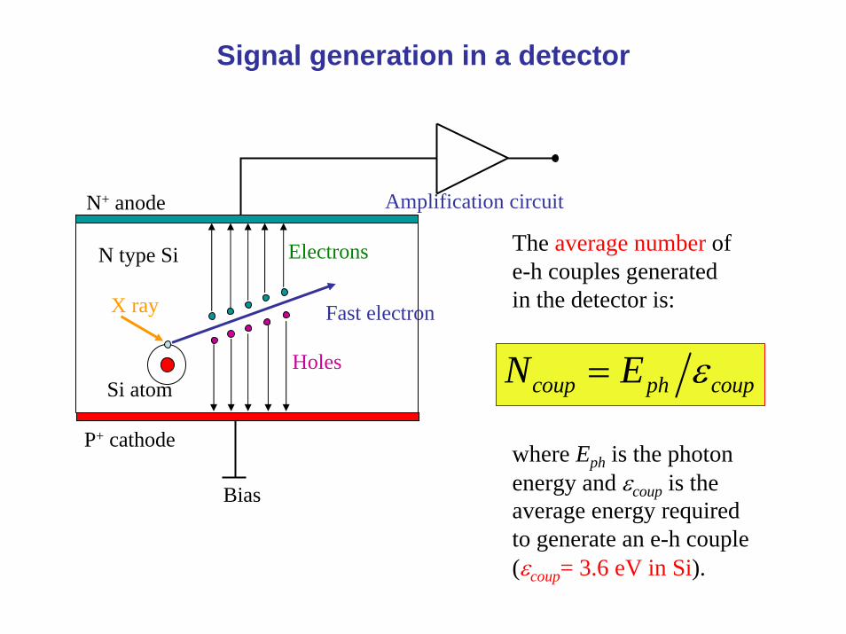
Signal generation in a detector
Amplification circuit
Fast electron
Electrons
HolesSi atom
X ray
N type Si
N+ anode
P+ cathode
Bias
coup ph coupN E ε=
The average number of e-h couples generatedin the detector is:
where Eph is the photonenergy and εcoup is the average energy requiredto generate an e-h couple(εcoup= 3.6 eV in Si).
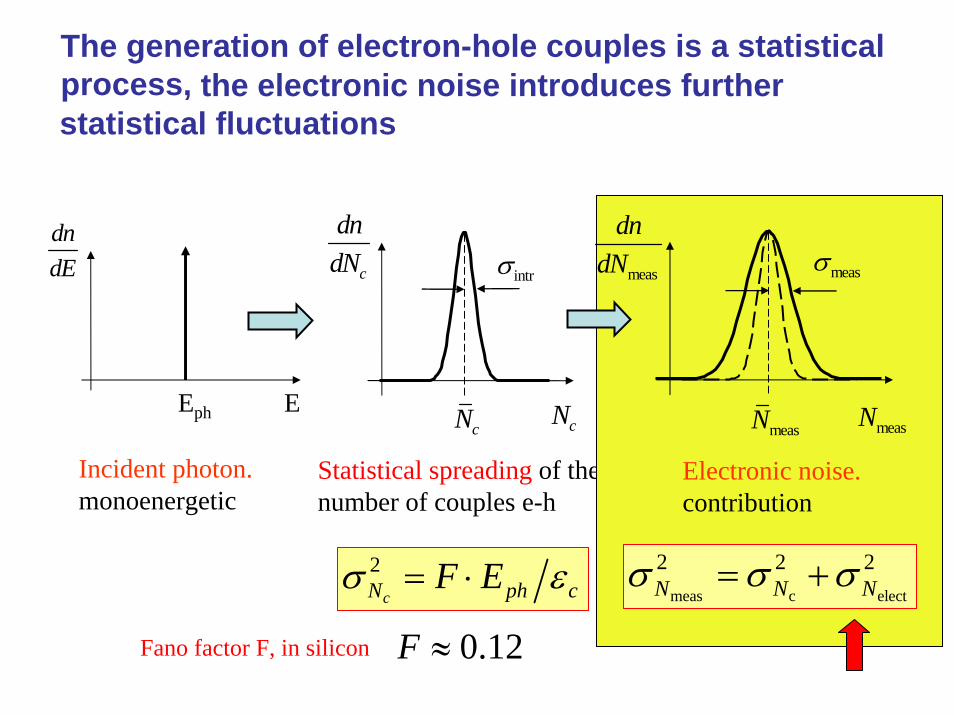
The generation of electron-hole couples is a statistical process, the electronic noise introduces further statistical fluctuations
Incident photon.monoenergetic
Eph E
dndE
2cN ph cF Eσ ε= ⋅
Statistical spreading of thenumber of couples e-h
Fano factor F, in silicon 0.12F ≈
c
dndN
cN cN
intrσ meas
dndN
measN measN
measσ
Electronic noise.contribution
meas c elect
2 2 2N N Nσ σ σ= +
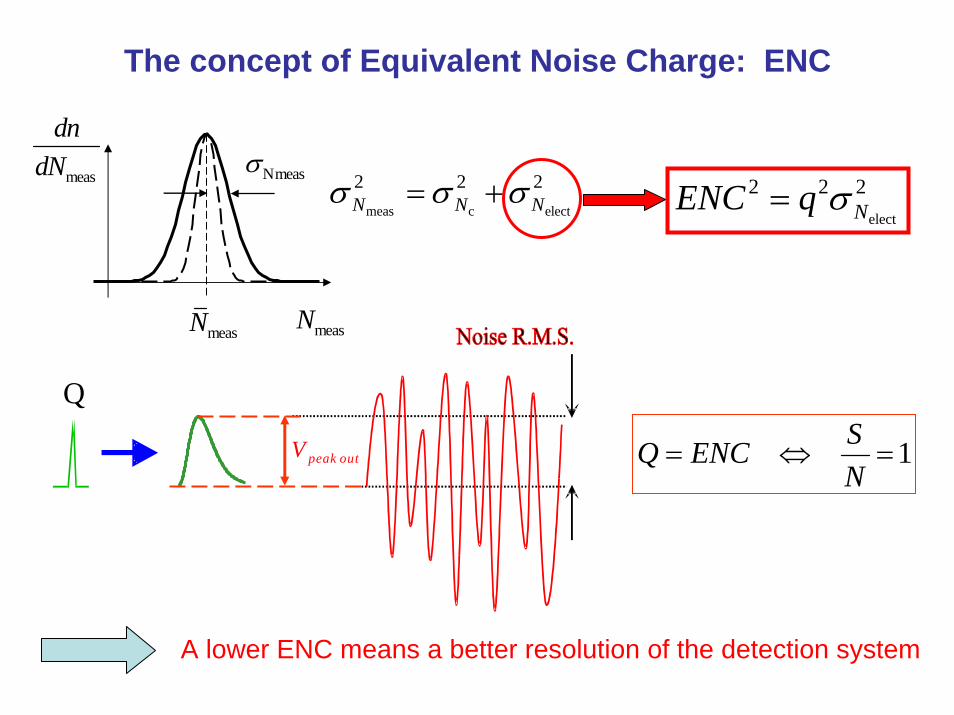
The concept of Equivalent Noise Charge: ENC
meas
dndN
measN measN
Nmeasσmeas c elect
2 2 2N N Nσ σ σ= +
elect
2 2 2NENC q σ=
Q
peak outV 1SQ ENCN
= ⇔ =
A lower ENC means a better resolution of the detection system
Signal and noisein the detection system
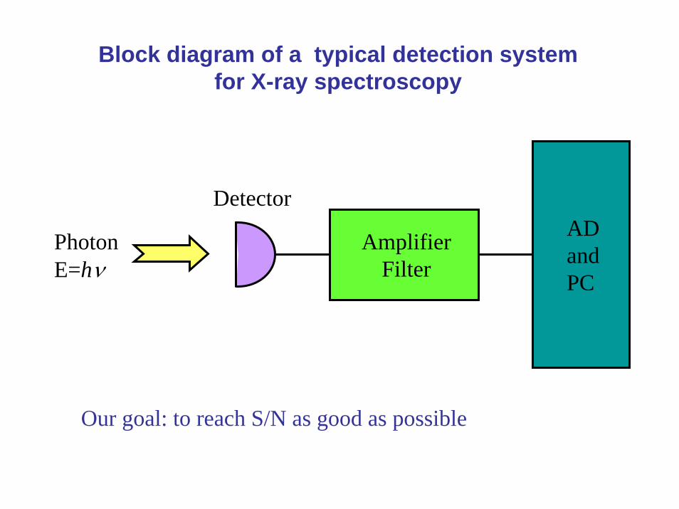
Block diagram of a typical detection system for X-ray spectroscopy
AmplifierFilter
ADandPC
Detector
PhotonE=hν
Our goal: to reach S/N as good as possible
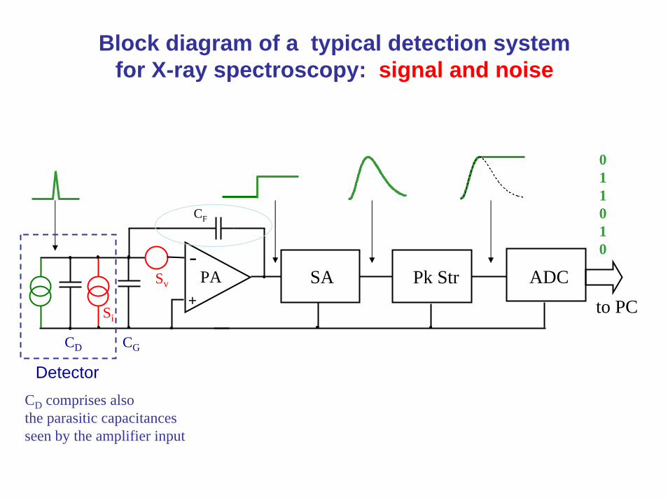
Block diagram of a typical detection system for X-ray spectroscopy: signal and noise
SA Pk Str ADCto PC
CD
-
+PA
Si
Sv
CG
CF
011010
DetectorCD comprises also the parasitic capacitancesseen by the amplifier input
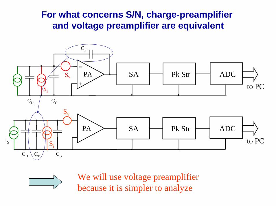
For what concerns S/N, charge-preamplifier and voltage preamplifier are equivalent
SA Pk Str ADCto PC
CD
-
+PA
Si
Sv
CG
CF
IS
PA SA Pk Str ADCto PC
CD CG
Sv
Si
CF
We will use voltage preamplifierbecause it is simpler to analyze
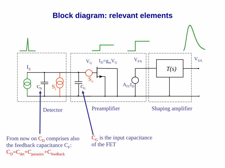
Block diagram: relevant elements
From now on CD comprises also the feedback capacitance CF:CD=Cdet+Cparasitic+Cfeedback
CG is the input capacitanceof the FET
T(s)
CGCD
IS
ID=gmVG
AIVID
Detector Preamplifier Shaping amplifier
VGVPA VSA
Si
Sv
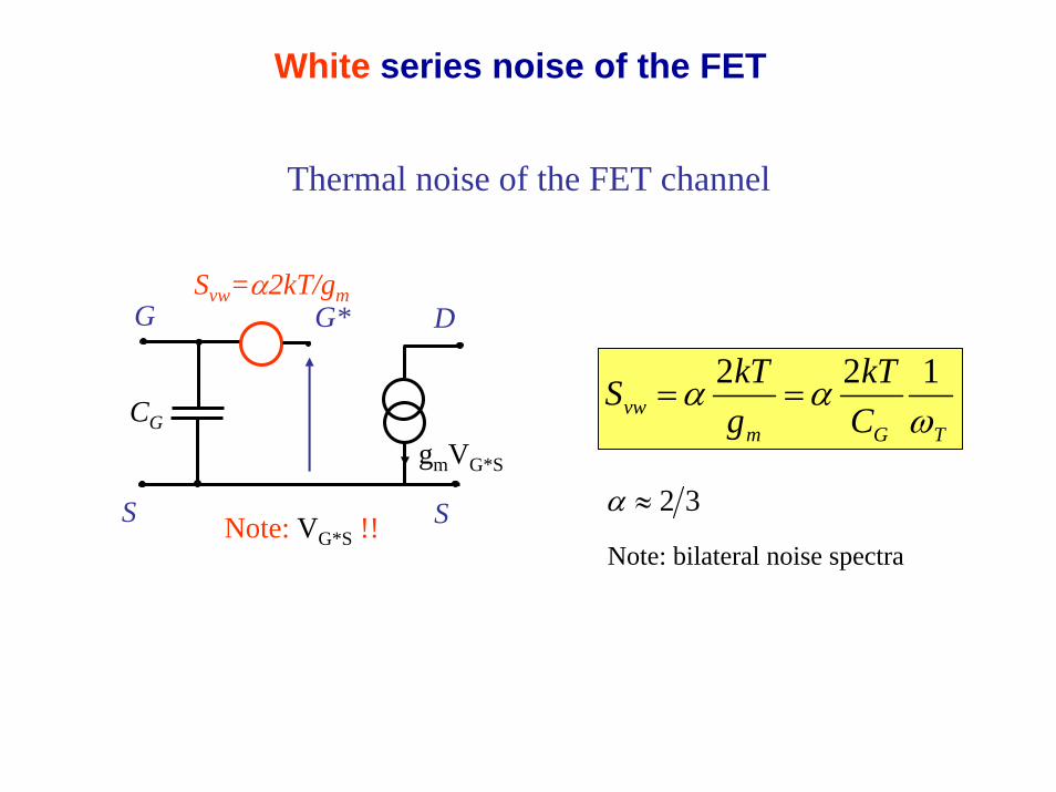
White series noise of the FET
Thermal noise of the FET channel
CG
Svw=α2kT/gmG G*
S
D
S
gmVG*S
Note: VG*S !!
2 2 1vw
m G T
kT kTSg C
α αω
= =
2 3α ≈
Note: bilateral noise spectra
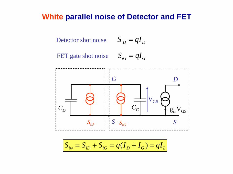
White parallel noise of Detector and FET
iD DS qI=Detector shot noise
iG GS qI=FET gate shot noise
CG
G
S
D
S
gmVGS
VGS
CD
SiD SiG
( )iw iD iG D G LS S S q I I qI= + = + =
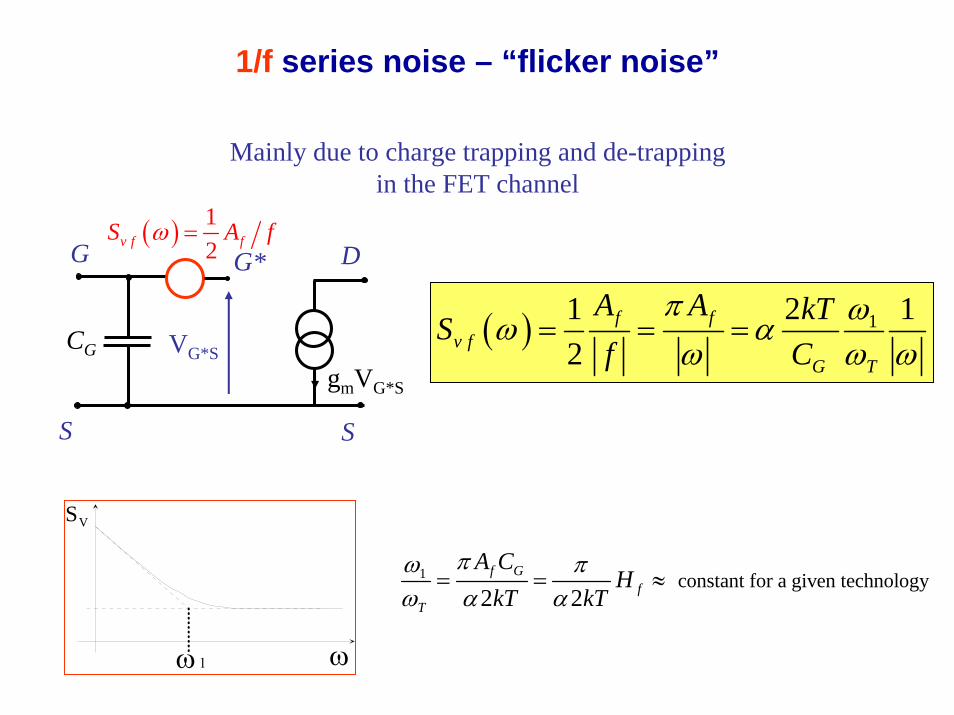
1/f series noise – “flicker noise”
Mainly due to charge trapping and de-trappingin the FET channel
( ) 11 2 12
f fv f
G T
A A kTSf C
π ωω αω ω ω
= = =CG
G G*
S
D
S
gmVG*S
VG*S
( ) 12v f fS A fω =
ωω 1
SV
1 constant for a given technology 2 2
f Gf
T
A CH
kT kTπω π
ω α α= = ≈
T(s)
CGCD
IDET
ID=gmVG
AIVID
Detector Preamplifier Shaping amplifier
VG
VPA VSA
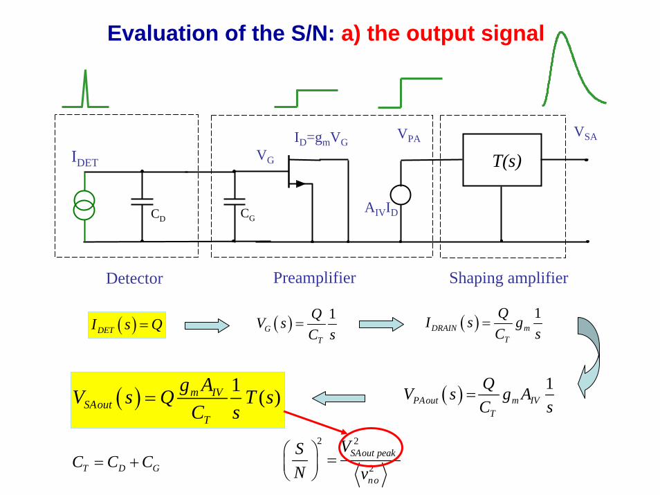
Evaluation of the S/N: a) the output signal
( )DETI s Q= ( ) 1DRAIN m
T
QI s gC s
=
( ) 1PAout m IV
T
QV s g AC s
=( ) 1 ( )m IVSAout
T
g AV s Q T sC s
=
( ) 1G
T
QV sC s
=
2 2
2SAout peak
no
VSN v
⎛ ⎞ =⎜ ⎟⎝ ⎠T D GC C C= +
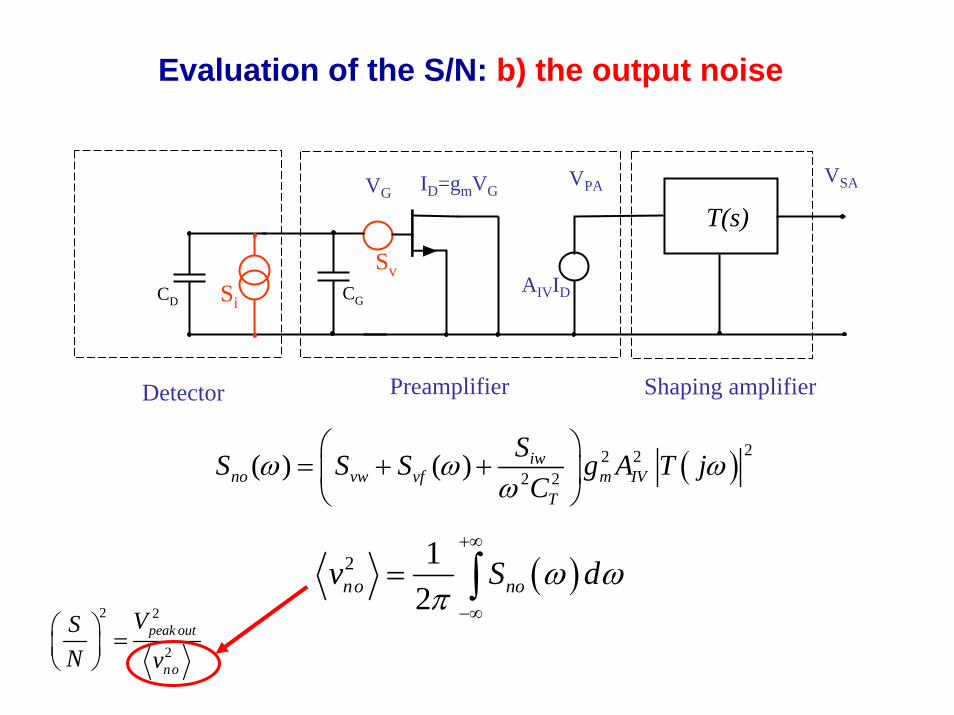
Evaluation of the S/N: b) the output noise
T(s)
CGCD
ID=gmVG
AIVID
Detector Preamplifier Shaping amplifier
VGVPA VSA
Si
Sv
( ) 22 22 2( ) ( ) iw
no vw vf m IVT
SS S S g A T jC
ω ω ωω
⎛ ⎞= + +⎜ ⎟⎝ ⎠
( )2 12no nov S dω ωπ
+∞
−∞
= ∫2 2
2peak out
no
VSN v
⎛ ⎞ =⎜ ⎟⎝ ⎠
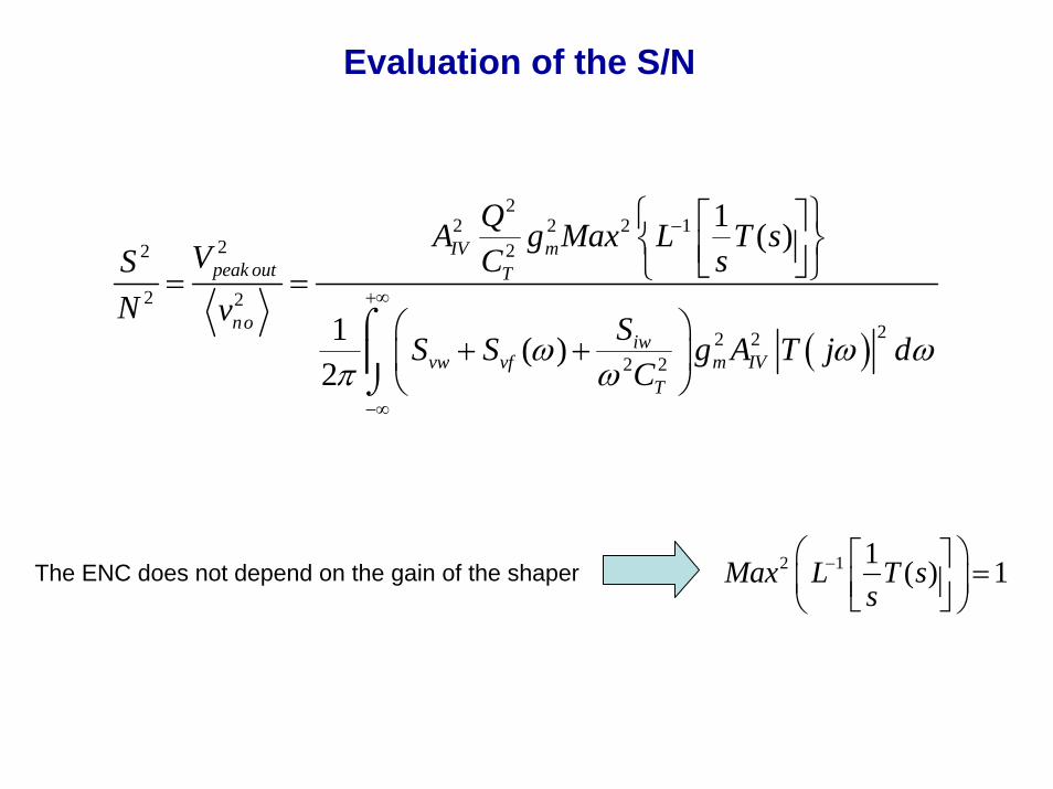
Evaluation of the S/N
( )
22 2 2 1
2 22
2 2
22 22 2
1 ( )
1 ( )2
IV mpeak out T
noiw
vw vf m IVT
QA g Max L T sV C sSN v SS S g A T j d
Cω ω ω
π ω
−
+∞
−∞
⎧ ⎫⎡ ⎤⎨ ⎬⎢ ⎥⎣ ⎦⎩ ⎭= =
⎛ ⎞+ +⎜ ⎟
⎝ ⎠
⌠⎮⌡
2 1 1 ( ) 1Max L T ss
−⎛ ⎞⎡ ⎤ =⎜ ⎟⎢ ⎥⎣ ⎦⎝ ⎠The ENC does not depend on the gain of the shaper

The Equivalent Noise Charge
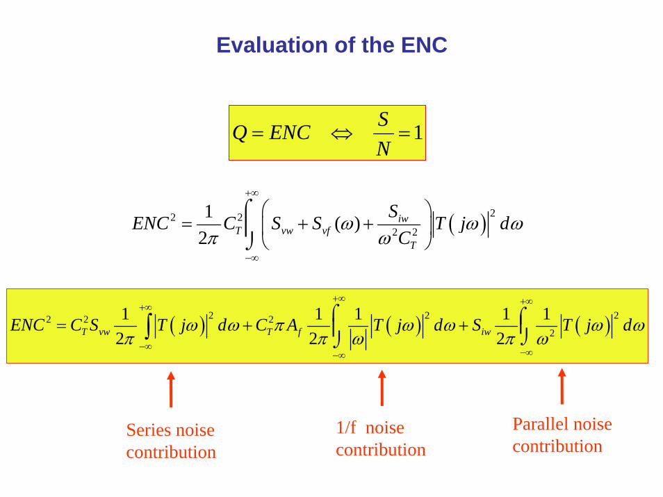
Evaluation of the ENC
1SQ ENCN
= ⇔ =
( ) 22 22 2
1 ( )2
iwT vw vf
T
SENC C S S T j dC
ω ω ωπ ω
+∞
−∞
⎛ ⎞= + +⎜ ⎟
⎝ ⎠
⌠⎮⌡
( ) ( ) ( )2 2 22 2 22
1 1 1 1 12 2 2T vw T f iwENC C S T j d C A T j d S T j dω ω π ω ω ω ωπ π ω π ω
+∞ +∞+∞
−∞ −∞−∞
= + +⌠ ⌠⎮⎮ ⌡⌡∫
Parallel noisecontribution
1/f noisecontribution
Series noisecontribution
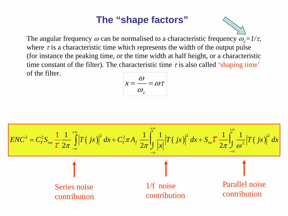
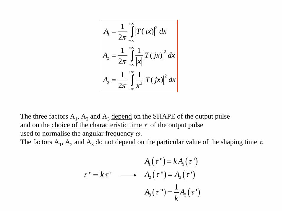
The “shape factors”
The angular frequency ω can be normalised to a characteristic frequency ωc=1/τ, where τ is a characteristic time which represents the width of the output pulse (for instance the peaking time, or the time width at half height, or a characteristic time constant of the filter). The characteristic time τ is also called ‘shaping time’of the filter.
c
x ω ωτω
= =
( ) ( ) ( )2 2 22 2 22
1 1 1 1 12 2 2
1T vw T f iwENC C S T jx dx C A T jx dx S T jx dx
xπ
π π π ωτ τ+∞ +∞+∞
−∞ −∞−∞
= + +⌠ ⌠⎮⎮ ⌡⌡∫
Parallel noisecontribution
1/f noisecontribution
Series noisecontribution
21
22
23 2
1 ( )2
1 1 ( )2
1 1 ( )2
A T jx dx
A T jx dxx
A T jx dxx
π
π
π
+∞
−∞
+∞
−∞
+∞
−∞
=
=
=
∫
∫
∫
The three factors A1, A2 and A3 depend on the SHAPE of the output pulse and on the choice of the characteristic time τ of the output pulse used to normalise the angular frequency ω. The factors A1, A2 and A3 do not depend on the particular value of the shaping time τ.
( ) ( )( ) ( )
( ) ( )
1 1
2 2
3 3
" '
" '1" '
A k A
A A
A Ak
τ τ
τ τ
τ τ
=
=
=
" 'kτ τ=
12 2
22
31
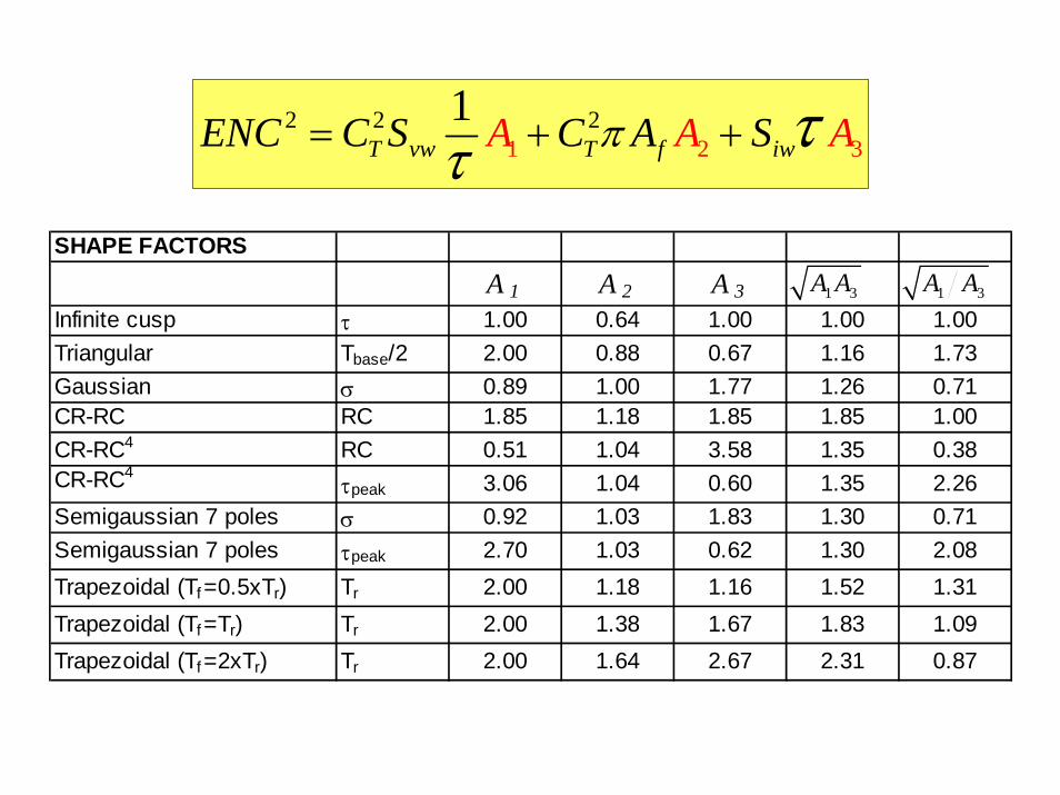
T vw T f iwE A ANC C S C A ASπτ τ= + +
SHAPE FACTORSA 1 A 2 A 3
Infinite cusp τ 1.00 0.64 1.00 1.00 1.00Triangular Tbase/2 2.00 0.88 0.67 1.16 1.73Gaussian σ 0.89 1.00 1.77 1.26 0.71CR-RC RC 1.85 1.18 1.85 1.85 1.00CR-RC4 RC 0.51 1.04 3.58 1.35 0.38CR-RC4
τpeak 3.06 1.04 0.60 1.35 2.26Semigaussian 7 poles σ 0.92 1.03 1.83 1.30 0.71Semigaussian 7 poles τpeak 2.70 1.03 0.62 1.30 2.08Trapezoidal (Tf =0.5xTr) Tr 2.00 1.18 1.16 1.52 1.31Trapezoidal (Tf =Tr) Tr 2.00 1.38 1.67 1.83 1.09Trapezoidal (Tf =2xTr) Tr 2.00 1.64 2.67 2.31 0.87
1 3A A 1 3A A
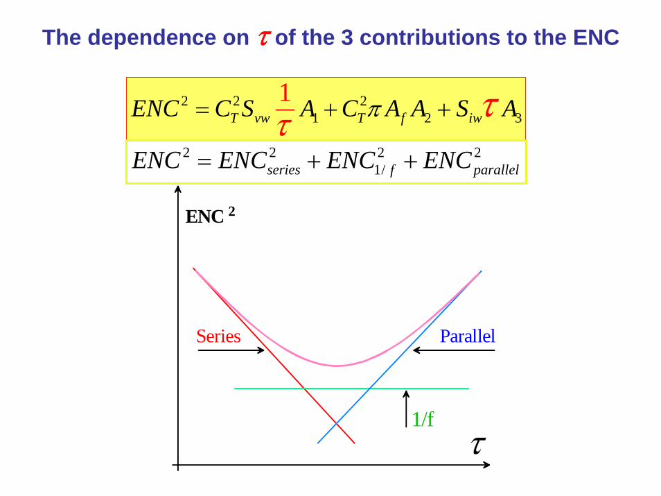
The dependence on τ of the 3 contributions to the ENC
2 2 21 2 3
1T vw T f iwENC C S A C A A S Aπτ τ= + +
2 2 2 21/series f parallelENC ENC ENC ENC= + +
Series
1/f
Parallel
τ
ENC 2
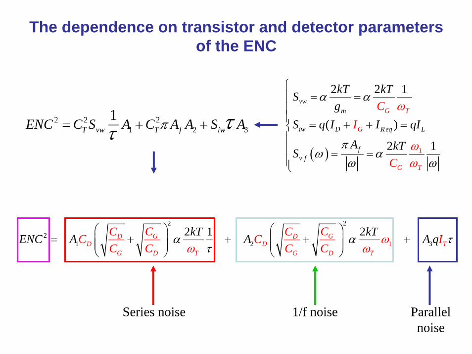
The dependence on transistor and detector parameters of the ENC
2 2 21 2 3
1T vw T f iwENC C S A C A A S Aπτ τ= + +
( ) 1
2 2 1
( )
2 1
vwm
iw D Req L
fv f
G T
G
G T
kT kTSg
S q I I qIC
I
CA kTS
ωα α
πω α
ωωω ω
⎧= =⎪
⎪⎪ = + + =⎨⎪⎪ = =⎪⎩
2 2
21 2 1 3
2 1 2G GD DD D T
G D T G D T
kT kTENC A AC CC CC C IC C
AC
qC
ωω ω
α α ττ
⎛ ⎞ ⎛ ⎞= + + + +⎜ ⎟ ⎜ ⎟⎜ ⎟ ⎜ ⎟
⎝ ⎠ ⎝ ⎠
Series noise 1/f noise Parallelnoise

How to optimise the ENC
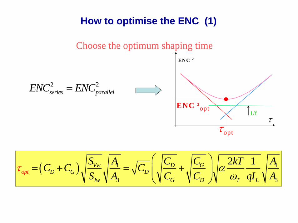
How to optimise the ENC (1)
Choose the optimum shaping time
2 2series parallelENC ENC=
1/fτ
ENC 2
ENC 2opt
τopt
( ) 1 1
3 3
2 1Vw GDD G D
Iw G D T Lopt
S CA C kT AC C CS A C C qI A
τ αω
⎛ ⎞= + = +⎜ ⎟⎜ ⎟
⎝ ⎠
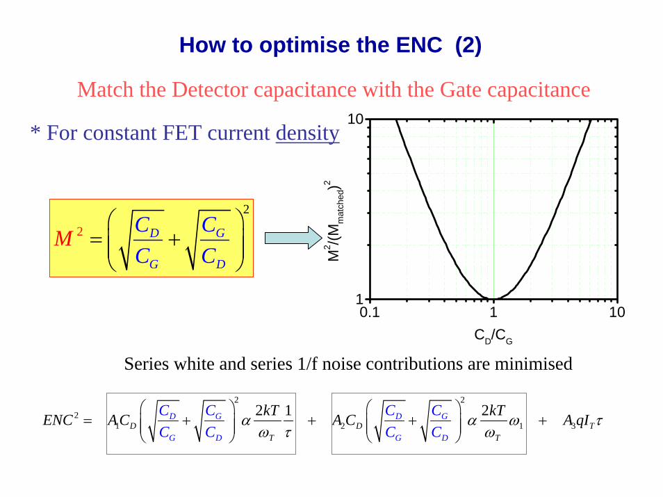
How to optimise the ENC (2)
Match the Detector capacitance with the Gate capacitance
2
2 GD
G D
CCC C
M⎛ ⎞
= +⎜ ⎟⎜ ⎟⎝ ⎠
Series white and series 1/f noise contributions are minimised
0.1 1 101
10
M2 /(M
mat
ched
)2CD/CG
* For constant FET current density
2 2
21 2 1 3
2 1 2G GD D
G D G DD D T
T T
kT kTENC AC A C AC CC CC C C C
qIα α ω τω τ ω
⎛ ⎞ ⎛ ⎞= + + + +⎜ ⎟ ⎜ ⎟⎜ ⎟ ⎜ ⎟
⎝ ⎠ ⎝ ⎠
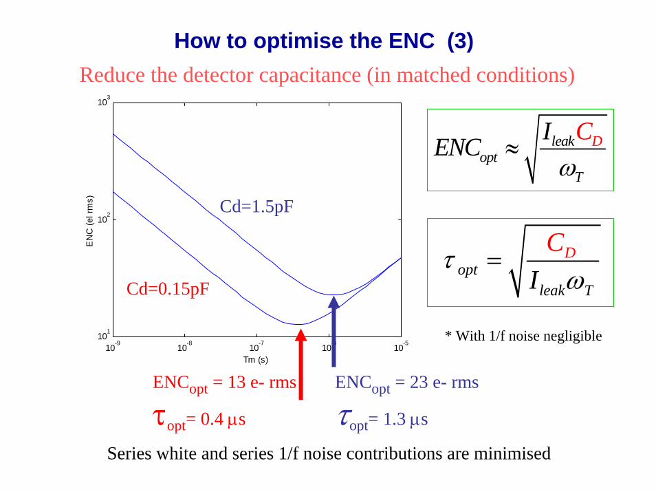
How to optimise the ENC (3)
10-9 10-8 10-7 10-6 10-5101
102
103E
NC
(el r
ms)
Tm (s)
Cd=1.5pF
Cd=0.15pF
Reduce the detector capacitance (in matched conditions)
leakopt
T
DIEN CCω
≈
optleak T
D
ICτω
=
* With 1/f noise negligible
ENCopt = 13 e- rms
τopt= 0.4 µs
ENCopt = 23 e- rms
τopt= 1.3 µs
Series white and series 1/f noise contributions are minimised
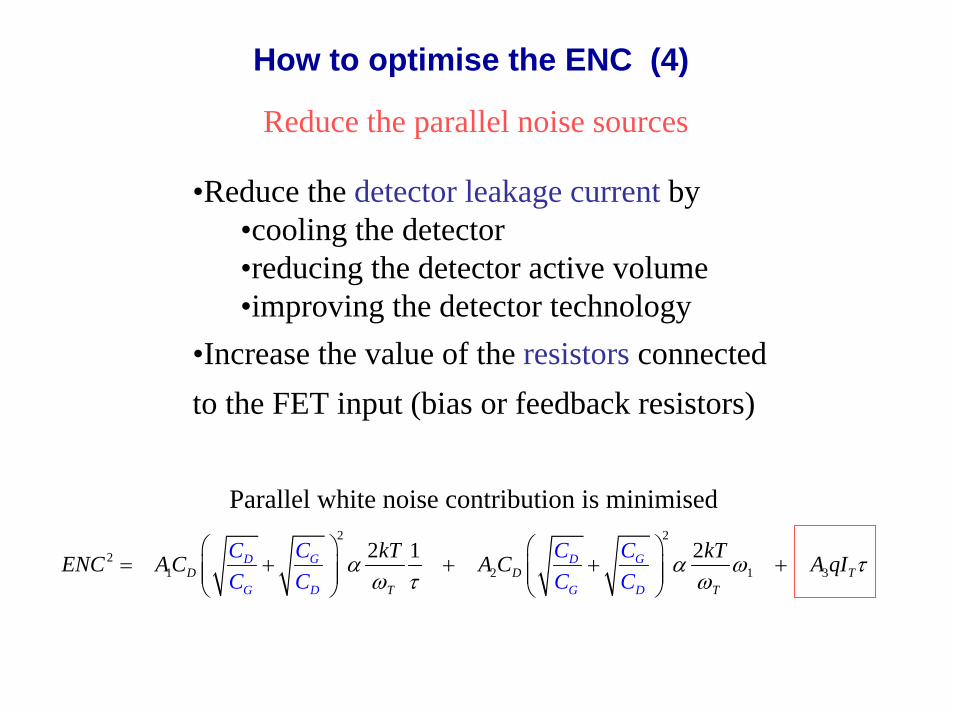
How to optimise the ENC (4)
Reduce the parallel noise sources
•Reduce the detector leakage current by•cooling the detector•reducing the detector active volume•improving the detector technology
•Increase the value of the resistors connectedto the FET input (bias or feedback resistors)
Parallel white noise contribution is minimised2 2
21 2 1 3
2 1 2G GD D
G D G DD D T
T T
kT kTENC AC A C AC CC CC C C C
qIα α ω τω τ ω
⎛ ⎞ ⎛ ⎞= + + + +⎜ ⎟ ⎜ ⎟⎜ ⎟ ⎜ ⎟
⎝ ⎠ ⎝ ⎠
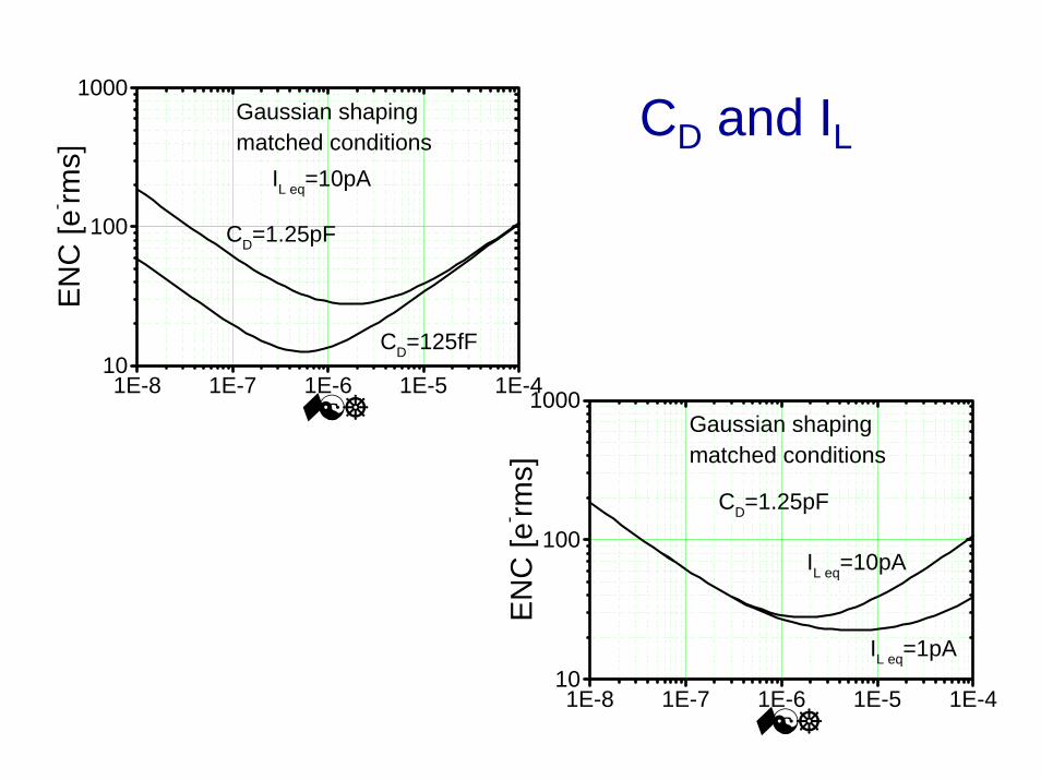
1E-8 1E-7 1E-6 1E-5 1E-410
100
1000
IL eq=10pA
IL eq=1pA
CD=1.25pF
Gaussian shapingmatched conditions
EN
C [e
- rms]
☯s
1E-8 1E-7 1E-6 1E-5 1E-410
100
1000
IL eq=10pA
CD=1.25pF
CD=125fF
Gaussian shapingmatched conditions
E
NC
[e- rm
s]
☯s
CD and IL
How to optimise the ENC (5)
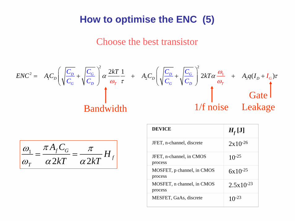
Choose the best transistor
2 2
21 3
12
2 1 2 ( )D DG G
GTD
DT
D D
G G D
C CC CC C C C
kTENC AC A C kT A I Iqατ ω
τωω
α⎛ ⎞ ⎛ ⎞
= + + + + +⎜ ⎟ ⎜ ⎟⎜ ⎟ ⎜ ⎟⎝ ⎠ ⎝ ⎠
Bandwidth 1/f noiseGate
Leakage
1
2 2f G
fT
A CH
kT kTπω π
ω α α= =
DEVICE Hf [J]
JFET, n-channel, discrete 2x10-26
JFET, n-channel, in CMOS process
10-25
MOSFET, p channel, in CMOS process
6x10-25
MOSFET, n channel, in CMOS process
2.5x10⁻²³
MESFET, GaAs, discrete 10-23
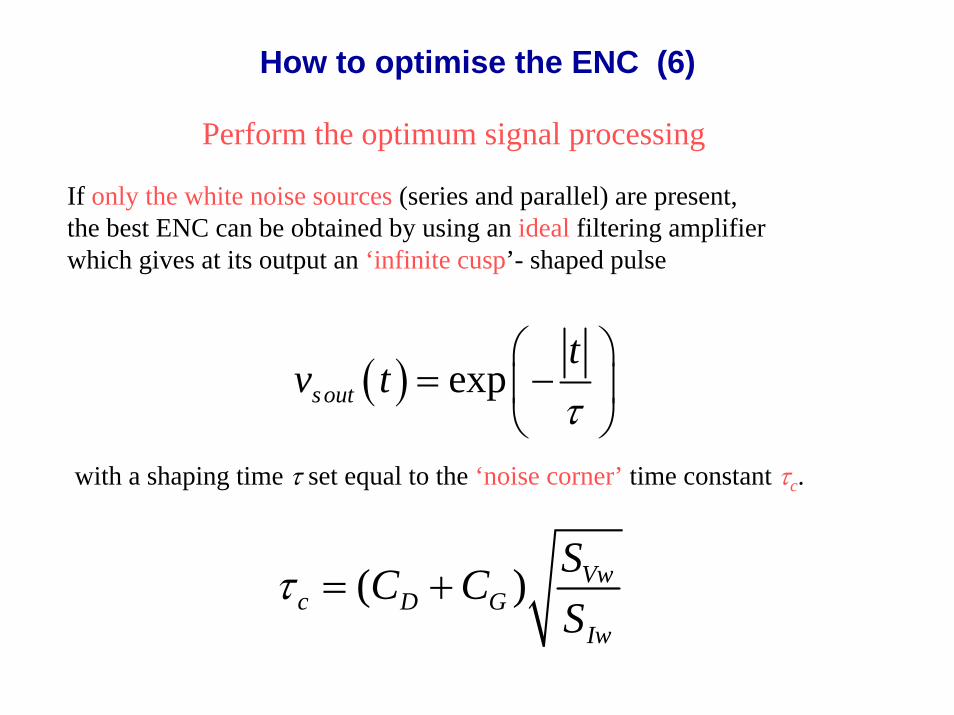
How to optimise the ENC (6)
Perform the optimum signal processing
If only the white noise sources (series and parallel) are present,the best ENC can be obtained by using an ideal filtering amplifierwhich gives at its output an ‘infinite cusp’- shaped pulse
( ) expsout
tv t
τ⎛ ⎞
= −⎜ ⎟⎝ ⎠
with a shaping time τ set equal to the ‘noise corner’ time constant τc.
( ) Vwc D G
Iw
SC CS
τ = +
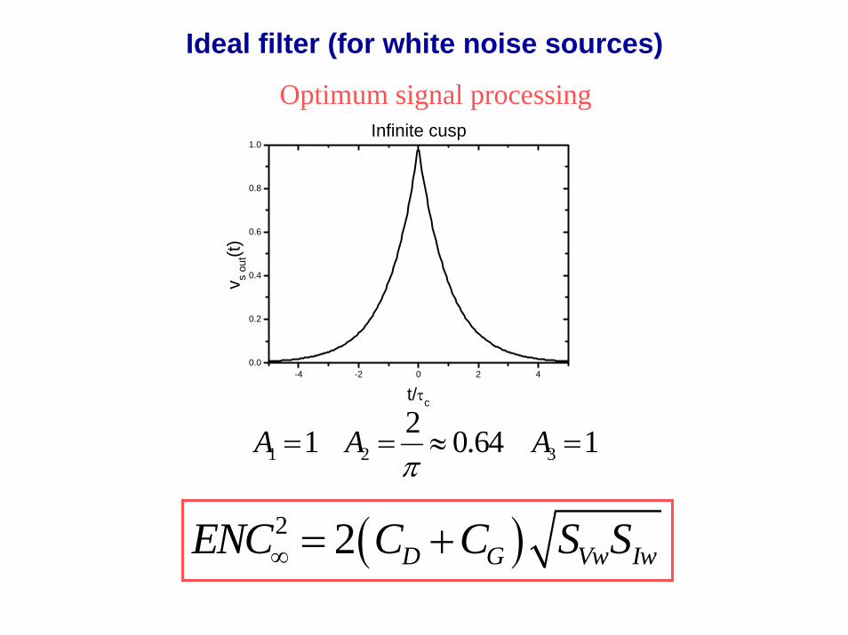
Ideal filter (for white noise sources)
Optimum signal processing
-4 -2 0 2 40.0
0.2
0.4
0.6
0.8
1.0Infinite cusp
v s ou
t(t)
t/τc
1 2 321 0.64 1A A Aπ
= = ≈ =
( )2 2 D G Vw IwENC C C S S∞ = +
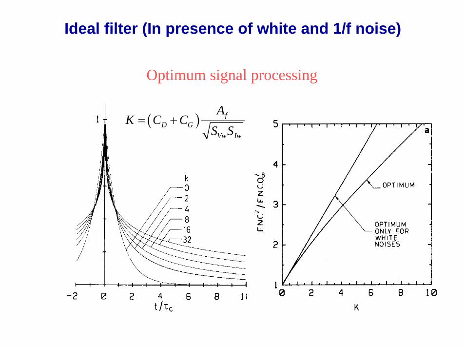
Ideal filter (In presence of white and 1/f noise)
Optimum signal processing
( ) fD G
Vw Iw
AK C C
S S= +
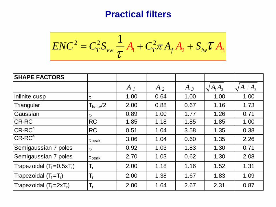
Practical filters
12 2
22
31
T vw T f iwE A ANC C S C A ASπτ τ= + +
SHAPE FACTORSA 1 A 2 A 3
Infinite cusp τ 1.00 0.64 1.00 1.00 1.00Triangular Tbase/2 2.00 0.88 0.67 1.16 1.73Gaussian σ 0.89 1.00 1.77 1.26 0.71CR-RC RC 1.85 1.18 1.85 1.85 1.00CR-RC4 RC 0.51 1.04 3.58 1.35 0.38CR-RC4
τpeak 3.06 1.04 0.60 1.35 2.26Semigaussian 7 poles σ 0.92 1.03 1.83 1.30 0.71Semigaussian 7 poles τpeak 2.70 1.03 0.62 1.30 2.08Trapezoidal (Tf =0.5xTr) Tr 2.00 1.18 1.16 1.52 1.31Trapezoidal (Tf =Tr) Tr 2.00 1.38 1.67 1.83 1.09Trapezoidal (Tf =2xTr) Tr 2.00 1.64 2.67 2.31 0.87
1 3A A 1 3A A
Appendix:Noise modelling
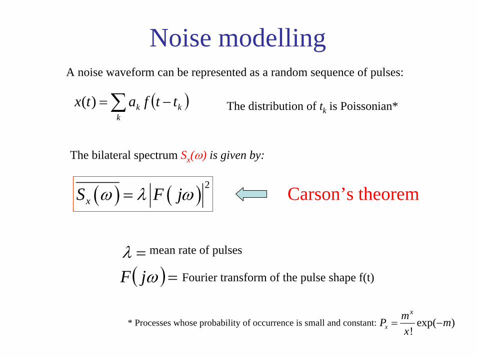
Noise modellingA noise waveform can be represented as a random sequence of pulses:
( )∑ −=k
kk ttfatx )( The distribution of tk is Poissonian*
The bilateral spectrum Sx(ω) is given by:
( ) ( ) 2xS F jω λ ω= Carson’s theorem
λ = mean rate of pulses
( ) =ωjF Fourier transform of the pulse shape f(t)
* Processes whose probability of occurrence is small and constant: exp( )!x
xmP mx
= −
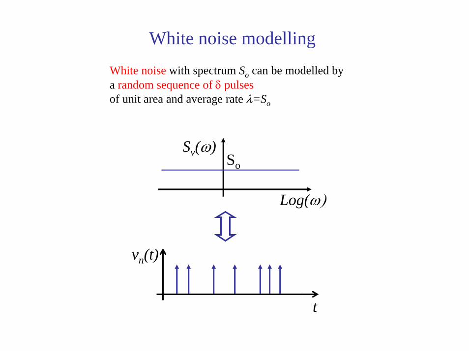
White noise modelling
White noise with spectrum So can be modelled by a random sequence of δ pulsesof unit area and average rate λ=So
Log(ω)
Sv(ω)So
vn(t)
t
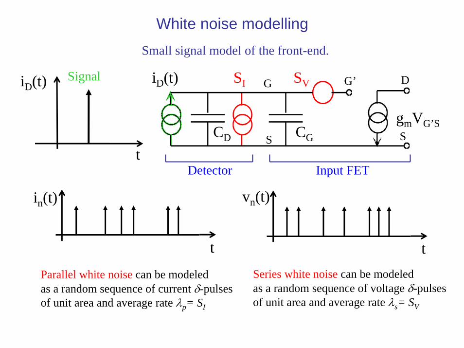
White noise modellingSmall signal model of the front-end.
SI SViD(t)
gmVG’SCGCD
Detector Input FET
G’ D
SS
G
t
iD(t) Signal
vn(t)
t
in(t)
tSeries white noise can be modeledas a random sequence of voltage δ-pulses of unit area and average rate λs= SV
Parallel white noise can be modeledas a random sequence of current δ-pulses of unit area and average rate λp= SI
White noise modelling
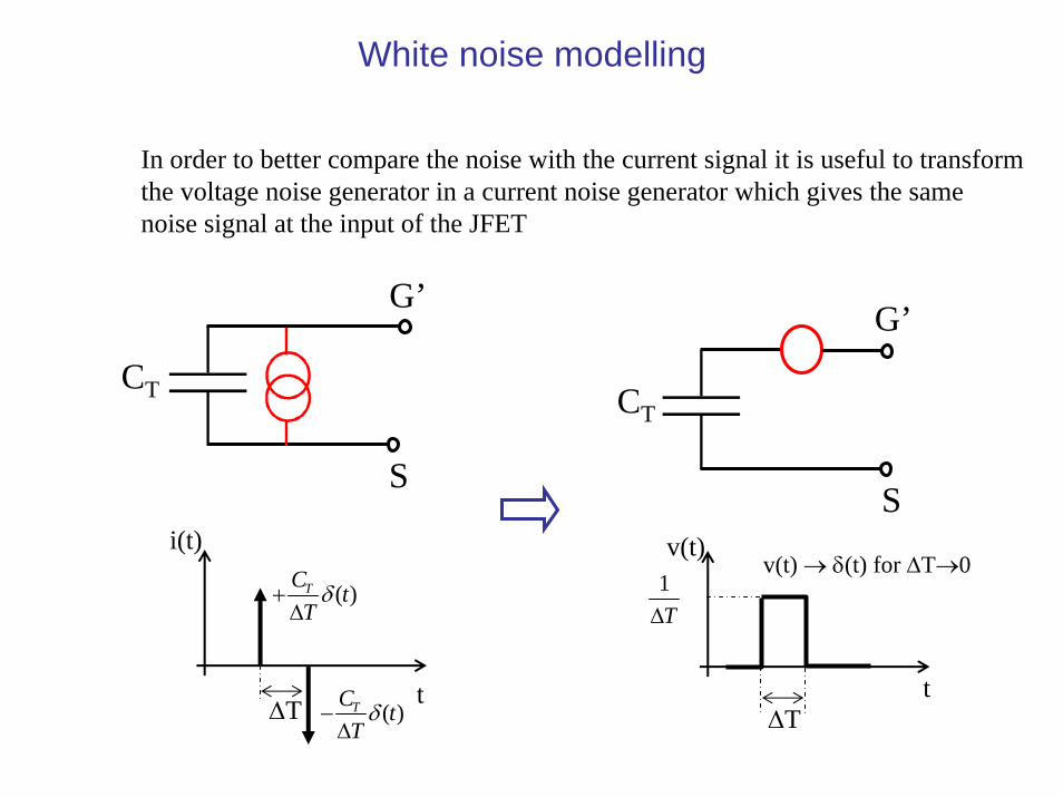
In order to better compare the noise with the current signal it is useful to transformthe voltage noise generator in a current noise generator which gives the samenoise signal at the input of the JFET
S
G’
CT CT
G’
S
v(t) → δ(t) for ∆T→0
∆T
v(t)
t
1T∆
∆T
i(t)
t
( )TC tTδ+
∆
( )TC tTδ−
∆
White noise modelling
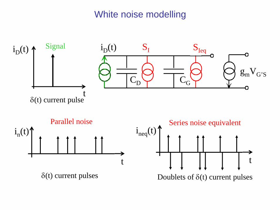
SI SIeqiD(t)
gmVG’SCGCD
t
iD(t) Signal
δ(t) current pulse
in(t)
t
Parallel noise
δ(t) current pulses
ineq(t)
t
Series noise equivalent
Doublets of δ(t) current pulses
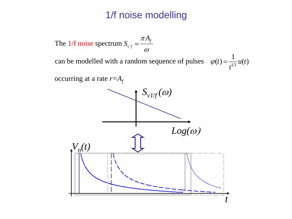
1/f noise modelling
The 1/f noise spectrum fv f
AS
πω
=
1 2
1( ) ( )t u tt
ϕ =can be modelled with a random sequence of pulses
occurring at a rate r=Af
Log(ω)
Sv1/f (ω)
t
Vn(t)
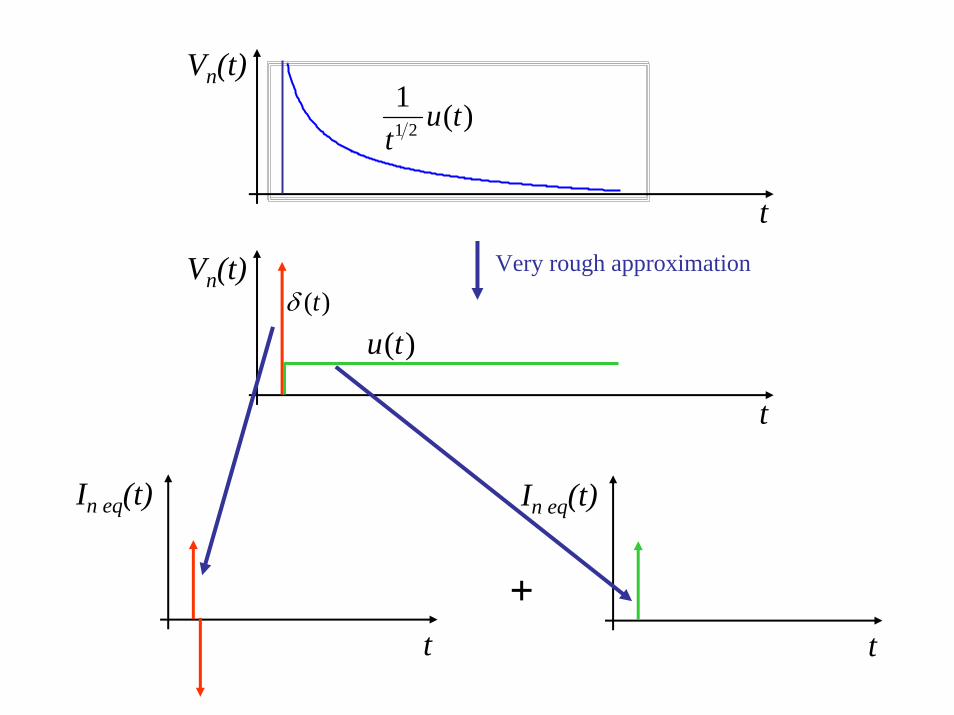
Vn(t)
t
)(tδ
)(tu
t
Vn(t))(1
21 tut
+t
In eq(t)
t
In eq(t)
Very rough approximation
The weighting function
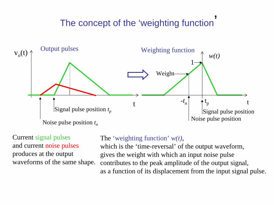
The concept of the ‘weighting function’
vo(t)
tSignal pulse position tp
Noise pulse position tn
Output pulses Weighting function
t
1
tp
w(t)
Signal pulse positionNoise pulse position
Weight
-tn
The ‘weighting function’ w(t),which is the ‘time-reversal’ of the output waveform,gives the weight with which an input noise pulse contributes to the peak amplitude of the output signal,as a function of its displacement from the input signal pulse.
Current signal pulsesand current noise pulsesproduces at the output waveforms of the same shape.
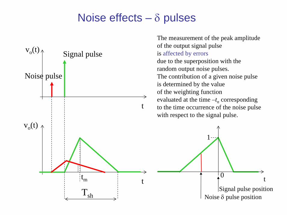
Noise effects – δ pulsesThe measurement of the peak amplitudeof the output signal pulseis affected by errorsdue to the superposition with the random output noise pulses.The contribution of a given noise pulse is determined by the value of the weighting functionevaluated at the time –tn correspondingto the time occurrence of the noise pulse with respect to the signal pulse.
t
vo(t) Signal pulse
Noise pulse
t
vo(t)
tm
Tsh
t
1
0
Signal pulse positionNoise δ pulse position
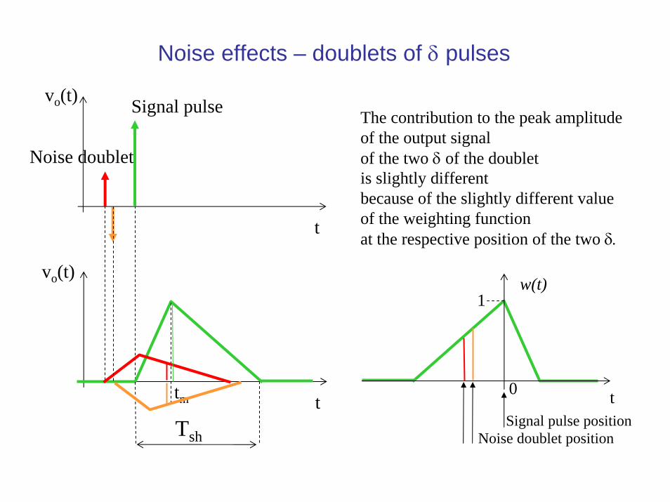
Noise effects – doublets of δ pulses
vo(t)
t
Signal pulse
Noise doublet
t
vo(t)
tm
Tsh
The contribution to the peak amplitudeof the output signal of the two δ of the doubletis slightly different because of the slightly different value of the weighting function at the respective position of the two δ.
w(t)
t
1
0
Signal pulse positionNoise doublet position
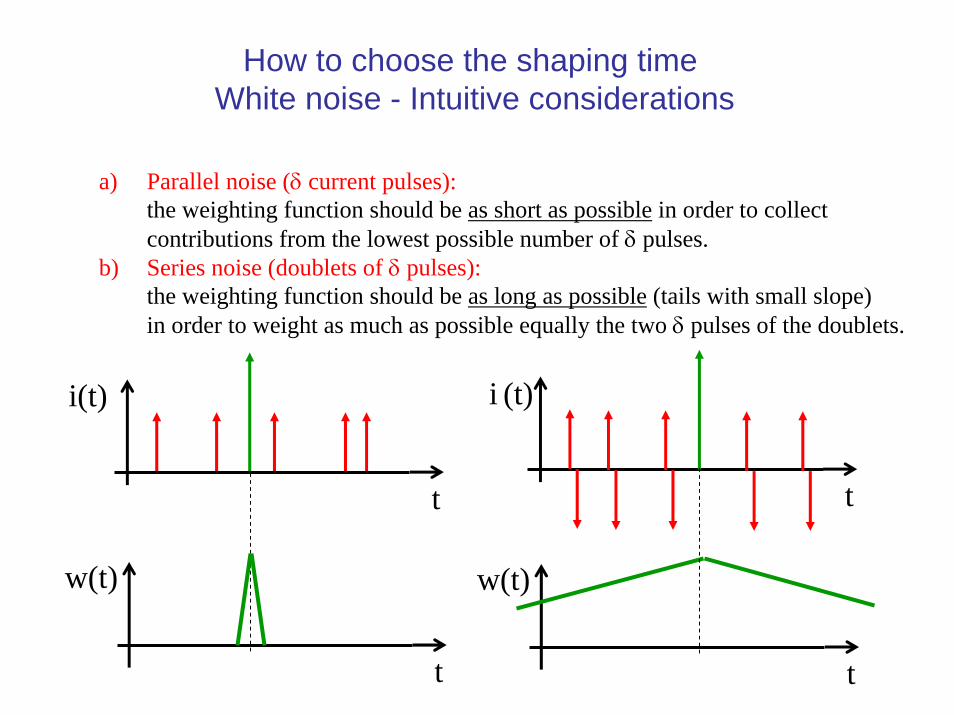
How to choose the shaping timeWhite noise - Intuitive considerations
a) Parallel noise (δ current pulses):the weighting function should be as short as possible in order to collectcontributions from the lowest possible number of δ pulses.
b) Series noise (doublets of δ pulses):the weighting function should be as long as possible (tails with small slope) in order to weight as much as possible equally the two δ pulses of the doublets.
i (t)
t
t
w(t)
i(t)
t
t
w(t)
How choose the shaping time 1/f noise - Intuitive considerations
t
In eq(t)
t
In eq(t)
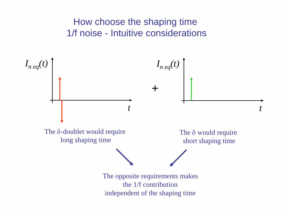
+
The δ-doublet would requirelong shaping time
The δ would requireshort shaping time
The opposite requirements makesthe 1/f contribution
independent of the shaping time


![agenda.infn.it · Web viewUn TDC per applicazioni nei sistemi PET, tenendo conto anche delle altre sorgenti di errore legate alle prestazioni dei rivelatori gamma [Moses 2006], necessita](https://img.pdfslide.tips/doc/110x75/5e608a97e8f8f50a1a2bf423/web-view-un-tdc-per-applicazioni-nei-sistemi-pet-tenendo-conto-anche-delle-altre.jpg)