Embed Size (px)
Citation preview
Sede Amministrativa: Università degli Studi di Padova
Dipartimento di Scienze Chimiche
Scuola di Dottorato di Ricerca in Scienza e Ingegneria dei Materiali
XXV Ciclo
Materials and methods for modular microfluidic devices
Direttore della Scuola: Ch.mo Prof. Gaetano Granozzi
Supervisore: Ch.mo Prof. Camilla Ferrante
Dottorando: Nicola Rossetto

I
Abstract (English version)
This thesis work concerns the investigation of materials and methods that can be applied
to the realization of microfluidic devices (MFDs). In particular, the attention is placed
on modular MFDs, as opposed to fully integrated ones. The reasons behind this choice
are given in detail in Section 1.2 of this work, but they can be here summarized in the
fact that while integrated MFDs offer great advantages in terms of portability, modular
devices are more versatile, and so particularly well suited for research applications.
The first part of the work here reported describes the microfabrication techniques
employed for the realization of single-function microfluidic modules. Devices have
been fabricated through PDMS replica molding from SU-8 masters. Masters have been
in turn realized through masked UV-lithography or one- or two-photon direct laser
writing, depending on the resolution requirements. The replica molding method is a
very fast and efficient way to realize MFDs, but suffers from some limitations in the
structure shapes that can be successfully replicated. In light of this, a
photopolymerizable hybrid organic/inorganic sol-gel blend is proposed and tested as
alternative material for MFDs fabrication. The characterization results reveal that this
material is biocompatible and features better mechanical properties than PDMS, but
structures with more than one dimension exceeding a few micrometers tend to crack
during fabrication, making this blend unusable as bulk material. Still, this material could
be efficiently employed to fabricate sub-structuration inside PDMS channels.
Following this investigation on materials, a microfluidic mixing module is proposed and
tested. Since laminar flow conditions dominate inside microchannels, efficient mixing
in MFDs require the use of specifically designed mixers. The proposed module makes
use of obstructions inside a microchannel to perturb the laminar flow and thus enhance
mixing of two species. The most efficient geometries have been selected with the aid of
numerical simulations, and two promising layouts have been fabricated and
Abstract (English version)
II
experimentally tested by measuring the dilution of a fluorophore (mixing between a
fluorophore solution and pure solvent) through confocal fluorescence microscopy.
Thirdly, the fabrication and characterization of an optofluidic light switching module is
reported. This device employs a water/air segmented flow generated by a T-junction to
alternatively transmit or total-reflect a laser beam. This deflection is proved to be
periodical, and its frequency can be varied nonlinearly by adjusting the injection flow
rates of air and water. The duty cycle of the module is also characterized, and a method
to modulate it by increasing the water temperature is proposed and verified.
Finally, a number of attempts to generate a nanoporous, low refractive index PDMS are
described. The identification of an efficient procedure to fabricate this kind of material
would lead to the possibility of using common microfluidic channels as water-core
waveguides. To date, these attempts have not been totally successful, but critical points
are identified, and viable strategies for future works on the subject are proposed.
III
Abstract (Versione italiana)
Questo lavoro di tesi tratta dello studio di materiali e metodi che possono essere
applicati alla realizzazione di dispositivi microfluidici (DMF). In particolare
l’attenzione è rivolta ai dispositivi modulari, piuttosto che a quelli altamente integrati.
Le ragioni dietro questa scelta sono spiegate in dettaglio nella Sezione 1.2 di questa tesi,
ma possono essere qui sintetizzate nel fatto che anche se i DMF integrati offrono grandi
vantaggi in termini di dimensioni finali, i dispositivi modulari sono più versatili, e
quindi particolarmente utili per applicazioni nel campo della ricerca.
La prima parte del lavoro qui riportato descrive le tecniche di microfabbricazione
utilizzate per la realizzazione di moduli microfluidici monofunzionali. I dispositivi sono
stati realizzati per replica molding in PDMS a partire da master in SU-8. I master sono
stati a loro volta fabbricati tramite litografia UV con maschera oppure per scrittura laser
diretta ad uno o due fotoni, a seconda dei requisiti di risoluzione. Il replica molding è un
metodo molto rapido ed efficiente per realizzare DMF, ma presenta alcuni limiti per
quanto riguarda la forma delle strutture che è possibile replicare con successo. Alla luce
di questo, un sol-gel fotopolimerizzabile ibrido organico/inorganico viene qui proposto
e testato come materiale alternativo per la fabbricazione di DMF. I risultati della
caratterizzazione rivelano che questo materiale è biocompatibile e presenta proprietà
meccaniche migliori di quelle del PDMS, ma strutture con più di una dimensione
eccedente i pochi micrometri tendono a sviluppare cricche, cosa che impedisce
l’utilizzo di questo sol-gel come materiale massivo. Ciononostante, questo sol-gel
potrebbe venir efficacemente impiegato per la realizzazione di sottostrutturazioni
all’interno di canali microfluidici.
Dopo questo studio sui materiali, un modulo microfluidico per il mescolamento è
proposto e testato. Dato che le condizioni di flusso laminare sono dominanti all’interno
dei microcanali, per ottenere un mescolamento efficiente in un DMF è necessario
includere nel dispositivo un miscelatore specificatamente progettato. Il modulo proposto
Abstract (versione italiana)
IV
utilizza delle ostruzioni all’interno del microcanale per perturbare il flusso laminare e
quindi favorire il mescolamento. Con l’aiuto di alcune simulazioni numeriche, le
geometrie più efficienti sono state individuate, e due layout particolarmente promettenti
sono stati realizzati e caratterizzati sperimentalmente misurando la diluizione di un
fluoroforo (mescolamento tra una soluzione del fluoroforo e puro solvente) attraverso la
microscopia confocale di fluorescenza.
A seguire, viene riportata la fabbricazione e caratterizzazione di un modulo optofluidico
per la deflessione della luce. Questo dispositivo utilizza un flusso segmentato acqua/aria
generato da una giunzione a T per trasmettere o riflettere (per riflessione totale interna)
alternativamente un fascio laser. Questa alternanza è periodica, e la sua frequenza può
essere controllata variando la portata dei flussi iniettati di aria e acqua. Inoltre, il duty
cycle del modulo è stato caratterizzato, e viene proposto e verificato un metodo per
modularlo attraverso un aumento della temperatura dell’acqua.
Infine, vengono descritti alcuni tentativi di generare un PDMS nanoporoso con basso
indice di rifrazione. La messa a punto di una procedura efficiente per la fabbricazione di
questo genere di materiale porterebbe alla possibilità di usare i classici canali
microfluidici come guide d’onda. Al momento questi tentativi hanno avuto solo parziale
successo, ma i maggiori punti di criticità sono stati identificati, e vengono proposte
alcune strategie per il loro futuro superamento.
Contents
Introduction 3
Overview on Microfluidics
1.1 Microfluidic devices 7
1.2 Integrated vs modular devices 17
1.3 Microfluidic elements 21
1.4 Materials and fabrication techniques 29
1.5 Optofluidics 42
Microfabrication
2.1 Microfabrication with SU-8 and PDMS 53
2.2 Beyond PDMS 58
2.3 Direct laser writing with MPTMS 62
Microfluidic Mixer
3.1 Free diffusion mixing 75
3.2 Pillars passive mixer 78
Optofluidic Optical Switch
4.1 Module realization 87
4.2 Module characterization 91
Water-Core PDMS Waveguide
5.1 Porous PDMS claddings 99
5.2 Experimental attempts 102
Conclusions 107
Bibliography 111
Ringraziamenti 119

3
Introduction
Since their initial diffusion about 10 years ago, microfluidic devices (MFDs) have
captivated much attention in both academic and industrial environments. This interest is
due to the many advantageous characteristics of microfluidics for a number of different
applications ranging from chemical synthesis to sensing to sample characterization. The
inclusion of light exploitation inside microfluidic devices (optofluidics) further
expanded the field of applicability, and thus the attention given to this branch of
science.
Abreast with the design of progressively more complex MFDs, increasingly
sophisticated fabrication techniques have been developed to allow the actual realization
of such devices. To date, a vast range of materials can be microstructured with
resolutions ranging from hundreds of micrometers to hundreds or even tens of
nanometers. This possibility has in turn allowed the realization of extremely complex
devices with thousands of channels and fluidic elements like valves, pumps or mixers.
On the other end, such high integration is often tied to technical challenges that can
require much work to overcome. Because of this, the very last years have seen the
appearance of modular microdevices in which compactness and portability are slightly
reduced in exchange for increased flexibility and ease of fabrication. Following this
approach, instead of realizing a single, integrated microfluidic chip able to perform all
the operations required to obtain the final result, a number of free-standing, single-
function modules are connected to achieve the same end. The work reported in this
thesis follows this modular philosophy, and proposes two single-function modules,
along with the techniques to produce these and other microfluidic elements.
The first chapter (Overview on Microfluidics) offers a wide overview on the field of
microfluidics, starting with its applications and proceeding to describe the elements
most commonly present in a MFD along with the materials and fabrication techniques
used to realize them. Finally, a section is dedicated to the field of optofluidics.
Introduction
4
The second chapter (Microfabrication) explains the fabrication techniques used in this
work. The first part of the chapter describes the main procedure employed to realize the
modules shown in subsequent chapters, i.e. PDMS replica molding from masters
obtained through UV photolithography and direct laser writing. Following that, the
characterization of a new photopolimerizable hybrid organic/inorganic sol-gel material
is performed. This second material has better mechanical properties and chemical
resistance than PDMS, and is presented as a candidate for internal channel sub-
structurations that require these improved qualities.
The third chapter (Microfluidic Mixer) introduces the problem of mixing inside
microchannels. Due to the dominant laminar flow conditions, chaotic motion is strongly
inhibited in microdevices. Without specifically designed mixers, mixing can only
happen through free diffusion, a process too slow for many applications. A qualitative
demonstration of this is given in the first part of the chapter, followed by the
presentation of a mixing module based on a partially obstructed channel. The module
design is optimized through the use of numerical simulations, and two promising
layouts are experimentally tested using the dilution of a fluorescent molecule as
indicator of mixing efficiency.
The fourth chapter (Optofluidic Optical Switch) presents a light-controlling module
for optofluidic applications. This device exploits a water/air segmented flow to
alternatively transmit and total-reflect a laser beam shone on the channel. The result is a
periodic deflection of the light towards one of two well-defined directions. The response
in terms of frequency of the device to varying injection flow rates is characterized,
along with eventual variations in the duty cycle (fraction of the total period spent by the
laser beam in the reflected state). Since the duty cycle appears to be constant at all
tested flow rates, an alternative method to modulate it (a variation in water temperature)
is proposed and verified.
The fifth chapter (Water-Core PDMS Waveguide) describes a series of attempts to
realize a nanoporous, low refractive index PDMS. Such a material could be employed

Introduction
5
as cladding for a water-core waveguide, and the direct consequence would be the
possibility of using common microfluidic channels as optical waveguides. While these
first attempts have not been entirely successful, the most critical point have been
identified and discussed, and possible strategies for future works are presented.
Finally, the Conclusions offer a summary of the results obtained during this work, as
well as observation concerning the drawbacks and limitations of these materials and
modules.

7
Chapter 1
OVERVIEW ON MICROFLUIDICS
1.1 Microfluidic devices
Microfluidics can be defined as the field of science and technology concerning itself
with devices that employ tiny volumes of fluids, on the order of 10-6 to 10-15 liters[1].
While its origins go back to the first studies on capillaries, it can be stated without any
fear of denial that microfluidics enjoyed a true development only in the last 10 years.
This recent evolution is both due to new microfabrication technologies that allow
scientists to build complex devices and to the increasing awareness that the peculiar
behavior of fluids on such a small scale can be exploited in a vast number of possible
applications. All these particular features can be related to two characteristics of
microfluidic devices (MFDs): a very high surface to volume ratio and a low Reynolds
number.
Since MFDs (also known as “microfluidic chips”) work with such tiny amount of fluid,
it is unavoidable that the channels inside which the liquid flows will be very thin. This
directly translates into the high surface to volume ratio mentioned before. This
characteristic can be a welcome boon for any application that requires very fine control
over the fluid condition, since the small volume will ensure that any gradient present
will be very limited in extent. Also, the large superficial area allows easy access to the
fluid to support functions like heaters. Conversely, this also allows fast dispersion of
any undesired heat produced, for example, during a chemical reaction. Another
advantage related to using small quantities of fluid becomes evident when such fluid is
toxic, unstable or dangerous in any other way: if an accident occurs, the volume of fluid
involved is so minimal that the danger to the user is very limited. Finally, vast surfaces
mean that capillarity and, more in general, interfacial forces will be dominant over
volume-related ones like gravity. In other words, usually fluids inside MFDs do not
freely fall and the device works just the same even upside down.
Overview on Microfluidics
8
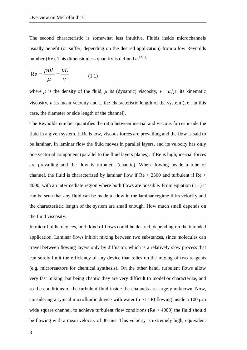
The second characteristic is somewhat less intuitive. Fluids inside microchannels
usually benefit (or suffer, depending on the desired application) from a low Reynolds
number (Re). This dimensionless quantity is defined as[2,3]:
Re uL uL
(1.1)
where is the density of the fluid, its (dynamic) viscosity, its kinematic
viscosity, u its mean velocity and L the characteristic length of the system (i.e., in this
case, the diameter or side length of the channel).
The Reynolds number quantifies the ratio between inertial and viscous forces inside the
fluid in a given system. If Re is low, viscous forces are prevailing and the flow is said to
be laminar. In laminar flow the fluid moves in parallel layers, and its velocity has only
one vectorial component (parallel to the fluid layers planes). If Re is high, inertial forces
are prevailing and the flow is turbulent (chaotic). When flowing inside a tube or
channel, the fluid is characterized by laminar flow if Re < 2300 and turbulent if Re >
4000, with an intermediate region where both flows are possible. From equation (1.1) it
can be seen that any fluid can be made to flow in the laminar regime if its velocity and
the characteristic length of the system are small enough. How much small depends on
the fluid viscosity.
In microfluidic devices, both kind of flows could be desired, depending on the intended
application. Laminar flows inhibit mixing between two substances, since molecules can
travel between flowing layers only by diffusion, which is a relatively slow process that
can sorely limit the efficiency of any device that relies on the mixing of two reagents
(e.g. microreactors for chemical synthesis). On the other hand, turbulent flows allow
very fast mixing, but being chaotic they are very difficult to model or characterize, and
so the conditions of the turbulent fluid inside the channels are largely unknown. Now,
considering a typical microfluidic device with water (~1 cP) flowing inside a 100 m
wide square channel, to achieve turbulent flow conditions (Re > 4000) the fluid should
be flowing with a mean velocity of 40 m/s. This velocity is extremely high, equivalent
Overview on Microfluidics
9
to a flow rate of 3.6 l/h, and this means that almost always the flow inside a
microchannel will be laminar. Thus, the flowing conditions of fluids inside MFD are
generally stable and often quite easy to predict. Unfortunately, laminar behavior also
means that spontaneous mixing inside a microchannel is almost always strongly
inhibited, and for many MFDs this can be a problem not easily solved (more on this
subject in Section 1.3.3).
1.1.1 Microreactors
One of the first developed applications for MFDs are microreactors, i.e. devices for
chemical synthesis. The reasons for this are quite straightforward, once considered the
characteristics of microdevices: the reaction conditions can be finely tuned and the
small volumes handled allow minimizing the danger of hazardous reagents or reactions.
Because of this, MFDs have been particularly studied for chemical processes that
involve explosive reagents or intermediates, or for reactions that synthesize toxic
products (e.g. chemotherapeutical drugs). As an example of handling potentially
dangerous reactions, deMello et al. have realized a microfluidic device for the
conversion of -terpinene into ascaridole[4]. This synthesis requires the use of strong
light to excite a sensitizing dye which in turn generates singlet oxygen from air or pure
oxygen. The gas reacts then with -terpinene (in methanol solution) to give ascaridole.
Unfortunately, oxygenated organic solvents are explosive, which means that in macro-
scale synthesis large volumes of dangerous reagents are formed during the process. In
the MFD oxygen, dye and -terpinene are all flowed inside a microchannel which is
placed under a light source. In this way only a tiny volume of oxygenated sample is
generated in any given moment, essentially removing safety concerns. Another example
comes from Zhang et al. and regards the use of ethyl diazoacetate[5]. This reagent is
flammable, and releases gaseous N2 if heated, resulting in an explosive behavior. The
authors proposed a microfluidic device for the ring-expansion reaction shown in Figure
1.1. This reaction is not only strongly exothermic, but also releases gaseous nitrogen as
Overview on Microfluidics
10
a secondary product, maximizing
the risk of vessel overpressure
and possibly explosion. Once
again, these hazards are greatly
reduced due to the small
volumes of reagents (which
minimize the amount of reactive
involved in case of incident) and to the high surface to volume ratio of the
microchannels, which provides rapid dissipation of generated heat. In general, it is
worth of note that in principle a microfluidic device can be a network of channels
completely isolated from the external environment, which makes MFDs the best
solution for user safety not only in case of incident, but also for day-to-day operations
involving toxic reagents. Of course, small volumes also mean small throughput, but this
limit can be overcome by using multiple MFDs in parallel. In this way, all the beneficial
characteristics are maintained for every single device, but the final throughput is
multiplied by the number of MFDs used.
Another useful characteristics of MFDs for chemical synthesis is the possibility of
generating dangerous reagents directly in situ. Since in a microdevice the reagents flow
along microchannels until they meet other substances, react and are then collected as
products, it is easy to imagine that a parallel channel on the same device can be used to
synthesize the dangerous or unstable substance that is then injected into the main
channel where the other reagents for the main reaction are flowing. Once again, this
approach can maximize operator safety. Kim et al. used a similar approach to perform a
series of reactions involving diazomethane[6]. Diazomethane is an extremely dangerous
gas, being toxic, carcinogenic and explosive (as well as odorless). The authors realized
a MFD featuring two parallel channels separated by a thin gas-permeable membrane.
The diazomethane is generated in situ in the first channel by reacting N-methyl-N-
nitroso-p-toluenesulfonamide (Diazald) with a strong base in aqueous solution. While
Figure 1.1: ring expansion reaction requiring ethyl diazoacetate. The explosive behavior of this reagent, added to the exothermic nature of the reaction makes microreactors the preferable vessel to handle this synthesis.
Overview on Microfluidics
11
reagents and secondary products continue along the channel and are collected as waste,
the gas migrates through the membrane to the adjacent channel, ready to react. The
authors tested various reactions by flowing different precursors in the second channel
and measuring the product yield at the outlet. As in the previous examples, risks for
operators are minimized by working (at any given moment) with only small quantities
of dangerous reagents, and in this case the hazardous species is created and reacted
inside the isolated environment of the MFD.
Microfluidic reactors also offer potential advantages from an industrial point of view.
Currently, most of the synthesis are done in large batch reactors. This poses several
disadvantages. First of all, it is difficult to maintain the exactly same conditions
(temperature, concentration, etc.) across all the reactor. MFDs can help solve this
problem, as already mentioned above. Also, batch reactors are necessarily discontinuous
processes, since the reactor must be filled with reagents, allowed to perform the reaction
and finally emptied of all products. On the contrary, a MFD is intrinsically continuous,
since reagents are pumped at the inlet, react as they flow and are finally collected at the
end of the channels network. From the industry point of view, the advantages of
continuous processes over discontinuous ones are quite evident: much less automation
is required and unproductive time losses are essentially eliminated.
An almost inescapable limitation of MFDs for chemical synthesis is their vulnerability
to channel clogging. Since typical microfluidic channels sport dimensions on the order
of hundreds of micrometers, any solid impurity that manages to get inside a MFD will
usually dam one of the channels, effectively ruining the device. While this problem is
usually not severe enough to require solvent filtration, it will bar any chemical reaction
that generate precipitate from being performed in MFDs. In theory, small amounts of
solid matter can be carried by the liquid flow without harm to the device, but this
practice is risky, since any unexpected increase in precipitate generation will probably
ruin the chip. Also, safeguards must be included in the pumping system, since a clogged
Overview on Microfluidics
12
channel will cause a strong overpressure inside the MFD, possibly to the point of
leakage of (potentially dangerous) reagents if not outright chip explosion.
1.1.2 Micro total analysis systems
Another field that has been vastly explored by microfluidic applications is that of
sample characterization. The interest for this kind of systems is so huge that “micro total
analysis system” (TAS) has basically become a synonym for “microfluidic device”.
These MFDs can be roughly divided in two broad categories: devices for quality control
and devices for the detection or characterization of analytes. The principles behind both
kind of devices are mostly the same, but the required characteristics for such MFDs can
be markedly different. The base idea upon which all these systems are founded is that of
creating a platform where the sample is injected at the inlet, analyzed while it flows
along the channels network and finally collected or disposed of (depending on the
destructiveness of the analysis) at the outlet.
Devices for quality control give their best when thought of in association with
microfluidic reactors. It is very easy to imagine a MFD where the product is synthesized
and immediately characterized just by adding the analysis system at the end of the
synthesis channel(s). More importantly, a feedback system can be implemented so that
any imperfection detected by the analysis translates immediately into a modification of
the reaction conditions until the proper product is once again synthesized. As before,
from an industrial point of view the advantages of these systems are noteworthy. As an
example, McMullen and Jensen realized a device composed of a first channel network
for chemical synthesis followed by an HPLC set-up to analyze the reaction products[7].
An automated optimization routine checks the characterization results and if necessary
modifies reaction parameters (solvent concentration, reaction time and temperature).
This device was used in particular to optimize the yield of intermediate benzaldehyde in
the benzyl alcohol to benzoic acid conversion.
Overview on Microfluidics
13
The main requirement from this kind of characterization devices is that the analysis
performed must be non-destructive, since it will be performed on the totality of the
product. Another important point is that the analysis should be fast. Even time-
consuming characterizations can be implemented in a MFD simply by increasing the
analysis channel length (and thus the time required for the fluid to pass through), but in
this case the feedback system will suffer from a possibly large delay, strongly
decreasing its efficiency. In light of these requirements, most of the quality control
devices are based on spectroscopic techniques. In the overwhelming majority of the
cases, the light is generated, collected and analyzed outside of the MFD due to the
difficulty of integrating such functions into a microdevice (but see Section 1.5). This
translates into the necessity for non-miniaturized equipment surrounding the device, but
this is typically of little consequence for an industrial set-up where these devices are not
meant to be moved. Alternatively, chromatographic systems, while more time-
consuming than spectroscopic ones, can double as purification steps and as such are
also object of frequent investigation.
Devices for detection or sample characterization feature a different set or requirements.
First of all they do not need the analysis to be either fast nor non-destructive. Both
qualities would be an add-on, but they are no longer a strict requirement since there is
no need for fast feedback, and only a part of the sample will be analyzed. This opens the
door for an enormous range of possible characterizations that can be implemented, from
electrochemical to chromatographic to colorimetric and so on. However, most of these
devices are intended to be moved quite often, and so need to be portable. This
immediately excludes light-based characterizations unless light source and detector can
be integrated into a chip (or are available everywhere, e.g. the sun as source and the eye
as detector). Obviously, in a portability contest MFDs have by their own nature a lead
start over most other devices, and so much of the research effort has gone into realizing
compact and portable TAS. Such a platform would be of great values for many
analysis (e.g. environmental) that currently are often made by collecting the sample on
Overview on Microfluidics
14
the field, transporting it to a lab and performing the analysis there. The possibility to
complete all the required steps directly on the field would be a great advancement in
terms of costs and time. On this subject, Beaton et al. realized a MFD for the
quantification of nitrite in seawater for environmental purposes[8]. The chip exploited a
colorimetric method (the Griess assay) to measure the analyte concentration. All the
device, including supporting instrumentation like power sources or detectors, was
included in a 16x30 cm cylinder, and its capabilities were demonstrated by a 57-hours
field test in ocean water.
There is another advantage of microdevices related to their small dimensions: only tiny
volumes of sample are required. This is of great importance when the analyte is
potentially dangerous or available only in small quantities, and makes MFDs
particularly interesting for forensic and medical applications (especially when
portability is added). It is also worth noting that if the analysis requires the addition of
reagents other than the sample, those too will only be required in small quantities. This
could be important when such additions are costly or, once again, potentially dangerous.
As an example, Liu et al. realized a MFD for forensic DNA analysis[9]. While the device
is not easily portable, its small channel volumes minimizes the amount of sample
needed to perform the analysis. Also, since most of the process is performed inside the
chip, operator interaction with the sample is almost eliminated. This has the great
advantage of reducing the risk of sample contamination.
1.1.3 Kinetic studies in microchannels
The high stability (and tunability) of reaction conditions inside microdevices makes
MFDs ideal systems for kinetic studies. Also, the flowing nature of these platforms
greatly simplifies the collection of data. Assuming that all involved reagents meet at a
certain point along a channel, the reaction will proceed while they are brought along by
the flow. This means that different places along the channel correspond to different
reaction times. This peculiar characteristic allows the implementation of an array of
Overview on Microfluidics
15
detectors to monitor the reaction progress, a much simpler method than the analysis of
samples extracted from the reaction batch at different times. In a MFD with an array of
detectors (e.g. photodiodes for light absorption measurements) at fixed distances from
one another, the sampling frequency (i.e. how much time elapses between successive
measurements) depends exclusively on the flow velocity inside the channel. By flowing
the reagents at high speed the sampling rate can in theory be extremely high (on the
order of hundreds of nanoseconds of reaction time between measurements or even less,
depending on the device).
The greatest drawback of microfluidics for this kind of application is related to the
laminar flow that dominates at these channel dimensions. The above description stems
from the assumption that all reagents are perfectly and instantaneously mixed at time
zero. Since in laminar conditions mixing can only be achieved through diffusion (a slow
process), real devices usually sharply diverge from this hypothesis. A common answer
is to include in the MFD a mixer (see Section 1.3.3), but in this case the dead volume of
the mixer reduces the time resolution of the device (that is, species start to mix when
they enter the mixer and are completely mixed when they exit; the time the flow needs
to clear the mixer degrades the time resolution of the device). Another solution is to
perform measurements only at the interface between the flows carrying the reagents.
Around the interface, mixing by diffusion is effectively instantaneous and the previous
assumption can be held. However, this method require the sampling probe (e.g. the light
beam for absorption measurements) to be small enough to sample only the
neighborhood of the interface.
An example of device for kinetics studies is provided by Voicu et al. in the form of a
MFD for the polymerization of N-isopropylacrylamide[10]. The chip is fitted to perform
attenuated total reflection Fourier transform infrared spectroscopy (ATR-FTIR) along
the channel just after the mixing step. This set-up allowed the authors to monitor the
effect of a vast range of reaction condition on the polymerization kinetics.
Overview on Microfluidics
16
1.1.4 Microfluidics for biology
The very last years have shown a previously unknown increase in interest by physicists,
chemists and engineers towards biology, and the field of microfluidics is no exception.
A staggering number of publications has appeared proposing various devices for cells
culturing and investigation. Once again, the small dimensions of microfluidic channels
come to aid. Tiny volumes mean that the environment conditions of the cell culture can
be finely determined and, if necessary, tuned. A continuous flow along the channels can
be used to bring nutrients to the cells while at the same time drawing away waste that
could in time poison and kill the culture. This function can be very easily automated,
reducing the time the scientist needs to devote to keeping the system viable. Finally, if
the cells must be subjected to treatment (e.g. staining, transfecting or lysing), only a
small amount of reagent is needed. Since chemicals for these applications are usually
quite expensive, this reduction can be quite advantageous.
Once the cells are grown and possibly treated, their analysis can be performed on the
chip. The most common methods of analysis in this field are optical ones, fluorescence
imaging above all, and they can be readily applied to a MFD. Even if direct integration
of optical instruments in the chip can be problematic at best, devices for cell culture and
analysis don’t usually require portability, so external optical system can be applied to
the MFD. Since cells are of the same order of dimension than microchannels (i.e. tens
of micrometers), they can be manipulated inside microdevices with relative ease. For
example, a suitably dimensioned channel can be used to assure that cells flow inside it
in a single file, ready to be analyzed one at a time.
A very common limitation of cells studies in macro is related to the fact that different
cell culture (even from the same cell line) cannot be always considered equivalent. This
is due to potential differences during their growth and multiplication, and has dramatic
repercussions for the researcher that desires to subject the same cell type to different
condition or reagents. In this case, the only macroscopic solution would be to grow a
large culture and then divide it between various isolated wells to treat them with
Overview on Microfluidics
17
different reagents. Obviously, such a procedure would be quite convoluted, and would
probably damage the culture. In a MFD, the solution is (once again) much simpler. A
cell culture can be grown along a network of channels and then, with the help of a
rationally designed system of inlets, only part of it can be subjected to every given
reagent. If necessary, the characteristic laminar flow featured by microdevices can be
invoked to ensure that different reagents can even travel along the same channel with
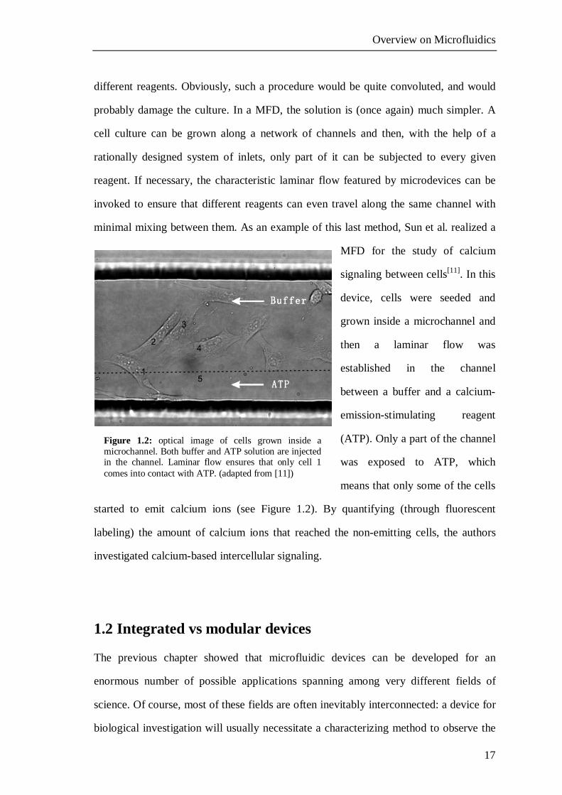
minimal mixing between them. As an example of this last method, Sun et al. realized a
MFD for the study of calcium
signaling between cells[11]. In this
device, cells were seeded and
grown inside a microchannel and
then a laminar flow was
established in the channel
between a buffer and a calcium-
emission-stimulating reagent
(ATP). Only a part of the channel
was exposed to ATP, which
means that only some of the cells
started to emit calcium ions (see Figure 1.2). By quantifying (through fluorescent
labeling) the amount of calcium ions that reached the non-emitting cells, the authors
investigated calcium-based intercellular signaling.
1.2 Integrated vs modular devices
The previous chapter showed that microfluidic devices can be developed for an
enormous number of possible applications spanning among very different fields of
science. Of course, most of these fields are often inevitably interconnected: a device for
biological investigation will usually necessitate a characterizing method to observe the
Figure 1.2: optical image of cells grown inside a microchannel. Both buffer and ATP solution are injected in the channel. Laminar flow ensures that only cell 1 comes into contact with ATP. (adapted from [11])
Overview on Microfluidics
18
system, just as a microreactor for chemical synthesis will benefit from on-line product
analysis. Thus, the categorization of microfluidics by their field of application is rough
at best and meaningless at worst. However, another kind of division can be considered,
one based not on the final purpose of the MFD but on how complex devices are
designed: integrated or modular microfluidics.
1.2.1 Integrated microfluidics
The integrated approach to microfluidics stems from the very captivating dream of
realizing a small, portable and monolithic device able to perform its designed function
without the need for any external equipment. The advantages of such a device are quite
evident: it can be used wherever and whenever needed, possibly even by untrained
personnel. Unfortunately, these undoubtedly desirable features come with a number of
disadvantages that must be considered, and challenges that must be overcome. First of
all, realizing a monolithic device able to perform complex operation is quite difficult,
especially if the dimensions of the various elements are on the order of micrometers.
This difficulty steeps even higher if the different functions needed by the final device
require different materials (e.g. metal for high pressure or glass for optical transparency)
that must be kept in airtight contact to prevent leakage. Another limitation is that if part
of the device stops working for any reason (e.g. a clogged channel, a quite likely
outcome if the device is used “on the field”), all the device must be replaced. Depending
on the fabrication process, this replacement could be quite expensive in terms of both
time and money. Finally, from the researcher point of view, it is not uncommon for a
prototype device that has been tested for some time to be scrapped in favor of a similar
one, usually because only one of several elements must be redesigned (e.g. a different
kind of mixer in a complex device for synthesis and characterization). When this
happens, there is a substantial chance that all the device must be redesigned to
accommodate the changes, especially if the modified element requires a different
material.
Overview on Microfluidics
19
In spite of these difficulties, the
overwhelming majority of
papers published on the subject
of microfluidics dwell on
integrated devices (or towards
them). This is of course
understandable, since if those
limitations could be overcome
the payback would be worth the
effort, with the achievement of
all the advantages described
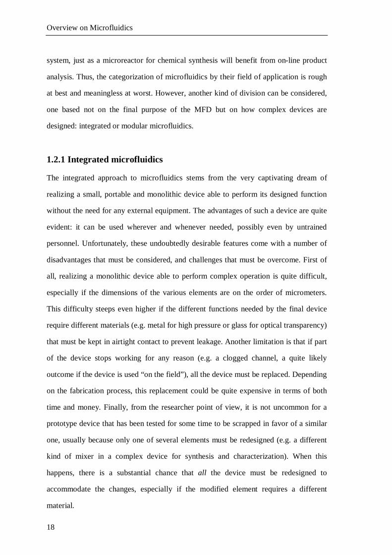
above. Lin et al. published a
review on such systems[12],
with particular focus on chips
for chemical synthesis. The
degree of complexity of such
devices is impressive, as can be seen for example in Figure 1.3. It must be noted,
however, that the photograph doesn’t show the external equipment that surrounds the
microfluidic chip. This is the greatest limitation of current integrated microdevices: they
still must be supported by external (macroscopic) instruments, mainly pumps but also
voltage generators or light sources as needed. While this restriction can be of no
consequence for synthesis microreactors (which are conceived not for portability but for
all the advantages described in Section 1.1.1), it means that the dream of a portable,
“black box” microsystem is still somewhere further in the future.
1.2.2 Modular microfluidics
Modular microfluidics is the other side on the MFD coin. In this approach, for every
elementary function needed in the device a free standing module is realized, and
Figure 1.3: photograph of a highly integrated microreactor able to perform 1024 different in situ click chemistry reactions. The tubing connected to the various inlets and outlets lead to external equipment (off image) like pumps or drains. (reproduced from [12])
Overview on Microfluidics
20
multiple modules are then connected to obtain the desired final result. The complete
device will be somewhat less compact than an integrated one, and the single modules
must be connected between them, adding a new challenge to the realization of the final
device, but the advantages are noteworthy. First of all, from the practical point of view,
if any module breaks down it can be singularly substituted, without the need to trash all
the device. Also, the design and actual realization are greatly simplified. Each module
can be designed without constrains due to functions present in other modules, and the
best material can be selected for each one while still avoiding the engineering nightmare
of integrating so many different materials in a single pseudo-monolithic piece. More in
general, each module can be designed without any regard for other modules, as long as
a suitable connection can be later established. This possibility is a boon for industrial
and/or scientific collaboration projects, since it allows every research unit to work on
his module without been affected by what happens in other units until the very end of
the project. The advantages for project coordination are self-evident, especially with the
added benefit that if unforeseen complications plague the work of one research unit, the
others can still proceed and, at worst, the final device will only lack one module.
Another good feature of modular microfluidics is that during device testing it is
relatively easy to change one element (by redesigning the specific module) while
leaving all the others intact, instead of been forced to recreate the whole device. Finally,
once a suitable “toolbox” of
single-function modules (like
pumps, mixers, reactors, and so
on) has been prepared, it is just a
matter of connecting any number
of them as needed to realize
hundreds of different devices.
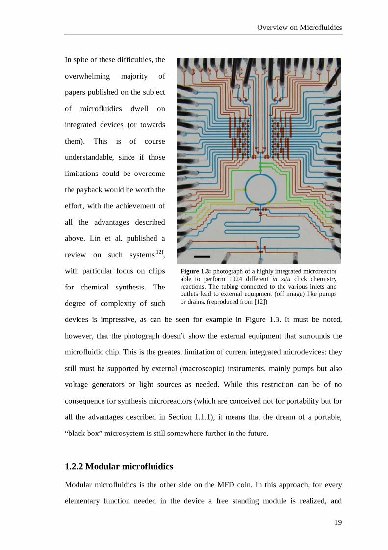
As an example of modular
approach to microfluidics, P. K.
Figure 1.4: photograph of a modular microfluidic device obtained by connecting different modules, each serving one specific function like reaction chamber or mixing step. (adapted from [13])
Overview on Microfluidics
21
Yuen created a platform where various functional elements (modules) can be freely
combined for a huge number of possible applications[13] (see Figure 1.4). In this work
the challenge of module connection was solved with a LEGO-like system in which
modules feature protruding outlets that leaklessly fit corresponding holes (inlets) in
adjacent elements. In addition to research works, a number of patents have been granted
in the last years concerning modular microfluidic devices[14–16].
1.3 Microfluidic elements
Whether a microfluidic device is made with a modular or integrated design, it will
necessarily consist of various functional elements. In the modular approach those
elements will be individual modules, and as such physically separated from one another,
while in an integrated device they will coexist in a single chip, but their function will
otherwise be the same. What follows is a description of the state of the art concerning
the most frequently used microfluidic functional elements, that is valves, pumps and
mixers.
1.3.1 Microfluidic valves
In any complex channel network valves are needed to control the direction of flow, and
microdevices are no exception. This is especially true with integrated devices, but also
modular ones often benefit from (or require) valves. Valves can be roughly divided in
two categories: active and passive. Active valves are operated by an external stimulus,
and are usually employed to bar the fluid from entering certain zones of the device at
the wrong time. Passive valves, on the other hand, work without any external input, and
are commonly used to allow flow in one direction but prevent backflow or to allow one
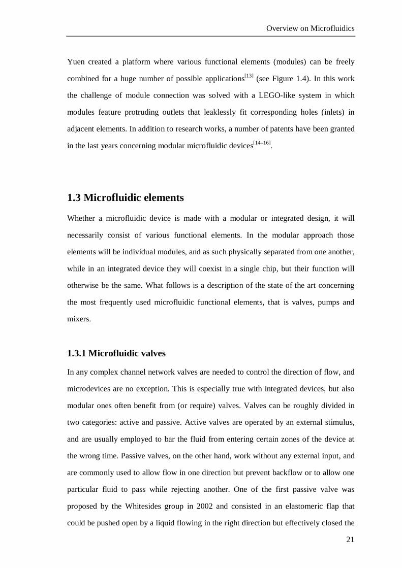
particular fluid to pass while rejecting another. One of the first passive valve was
proposed by the Whitesides group in 2002 and consisted in an elastomeric flap that
could be pushed open by a liquid flowing in the right direction but effectively closed the
Overview on Microfluidics
22
channel if the liquid flowed in the
opposite direction[17] (see Figure
1.5). This kind of valve can be
used to prevent backflow in a
MFD, and also allows the
realization of simple pumps (see
Section 1.3.2). A different type of
passive valve, one that
differentiate between fluids instead
of direction of flow, has been
proposed by Y. S. Song[18]. This
element consists in a microfluidic
channel filled with an agarose
hydrogel doped with carbon
nanotubes (to improve mechanical properties). This porous material will allow mineral
oil to flow through undisturbed. However, if water is flowed instead, the hydrogel will
swell, sealing the pores and blocking the channel. The modification is reversible, as
long as the valve is allowed to dry once swelled.
While passive valves have their applications, most of the recent MFDs rely on active
ones. The reason for this is that active valves are easier to fabricate and can be
controlled much better than passive ones, at the price of dependency on off-chip
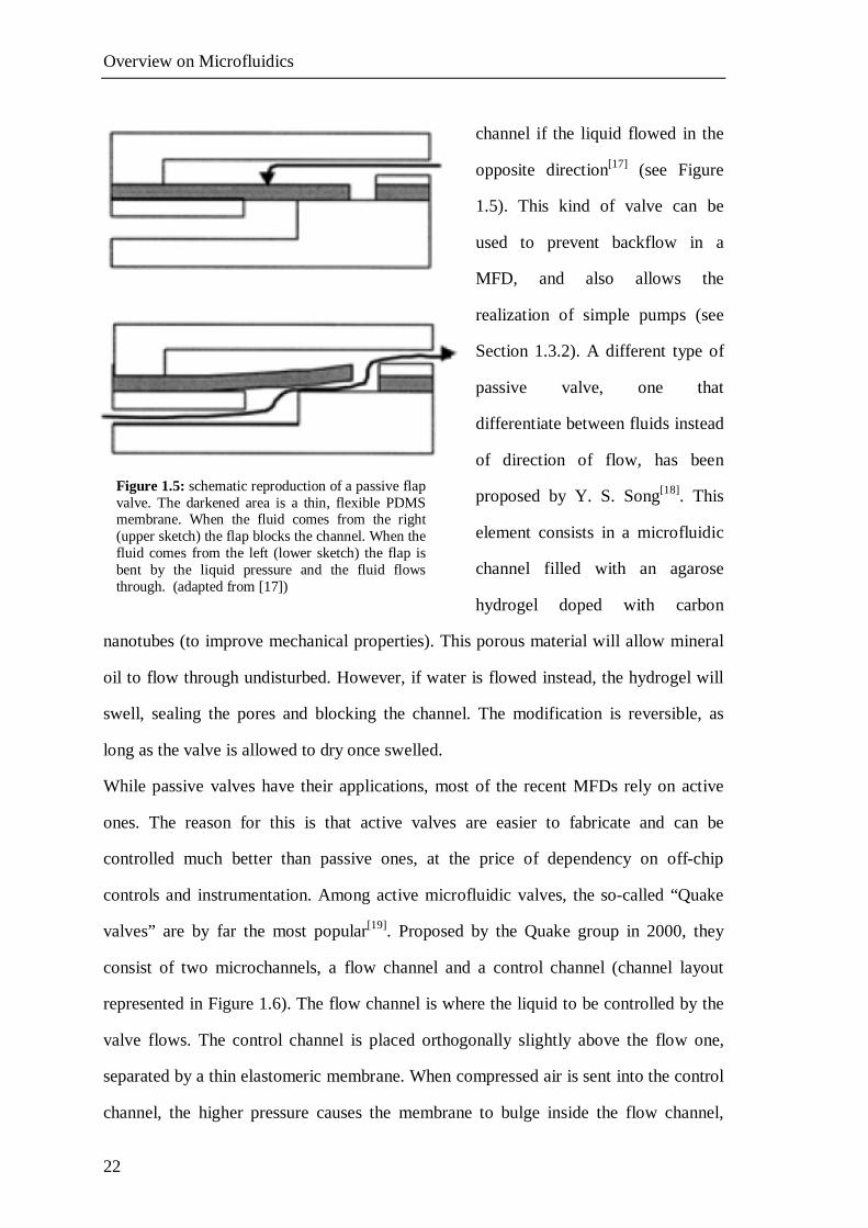
controls and instrumentation. Among active microfluidic valves, the so-called “Quake
valves” are by far the most popular[19]. Proposed by the Quake group in 2000, they
consist of two microchannels, a flow channel and a control channel (channel layout
represented in Figure 1.6). The flow channel is where the liquid to be controlled by the
valve flows. The control channel is placed orthogonally slightly above the flow one,
separated by a thin elastomeric membrane. When compressed air is sent into the control
channel, the higher pressure causes the membrane to bulge inside the flow channel,
Figure 1.5: schematic reproduction of a passive flap valve. The darkened area is a thin, flexible PDMS membrane. When the fluid comes from the right (upper sketch) the flap blocks the channel. When the fluid comes from the left (lower sketch) the flap is bent by the liquid pressure and the fluid flows through. (adapted from [17])
Overview on Microfluidics
23
effectively blocking it. Easy to
fabricate and to use, Quake valves
enjoy a (well-deserved) enormous
popularity among microfluidics
researchers, especially those that work
on highly integrated devices, since
active valves are critical to control
complex multi-functional devices. It is
far from uncommon to see highly
integrated MFDs featuring tens if not
hundreds of these valves[12].
In addition to those described, a great number of different valves have been proposed
for use in MFDs with varying success. Additional information can be found for example
in a comprehensive review article by K. Oh and C. Ahn[20].
1.3.2 Microfluidic pumps
All MFDs need a way to flow liquids inside the channels network. Most of the time this
requirement is accomplished by off-chip pumps that push fluids in the device through
an inlet. However, it would be greatly advantageous to transform the pumping system
from external support equipment to actual part of the MFD. The simplest method to
achieve fluid movement is to fabricate the channels with a material that is wetted by the
fluid, attach a reservoir at the beginning of the device and let the channels be filled
through capillarity. The drawback is immediately clear: once the channel is completely
filled, no additional flow is generated. Thus, this method can be readily implemented
for certain applications (e.g. throw-away devices for simple chemical analysis) but is
insufficient for many other. A similar, more versatile method is to place the device on a
rotating platform, place the inlet (and reservoir) at the center of the device and allow
centrifugal forces to spread the fluid from the inlet towards the border of the chip.
Figure 1.6: layout of a “Quake valve”. When compressed air is forced in the upper channel, it will deform and bulge in the lower, sealing it. (adapted from [19])
Overview on Microfluidics
24
Centrifugal microfluidics[21] have the advantage that the flow will continue even if the
channels are already filled (as long as an outlet is provided), and fluid flow speed can be
controlled by adjusting the rotation speed. This offers the possibility for additional
control. If the device is realized in a material that is not wetted by the fluid, to enter a
given channel the fluid will have to prevail against a force inversely proportional to the
channel diameter. Thus, smaller channels will be accessed only if the centrifugal force
(i.e. the rotation speed) exceed a certain minimum. A clever chip designer can exploit
this phenomenon to control how and when certain areas of the device are reached by the
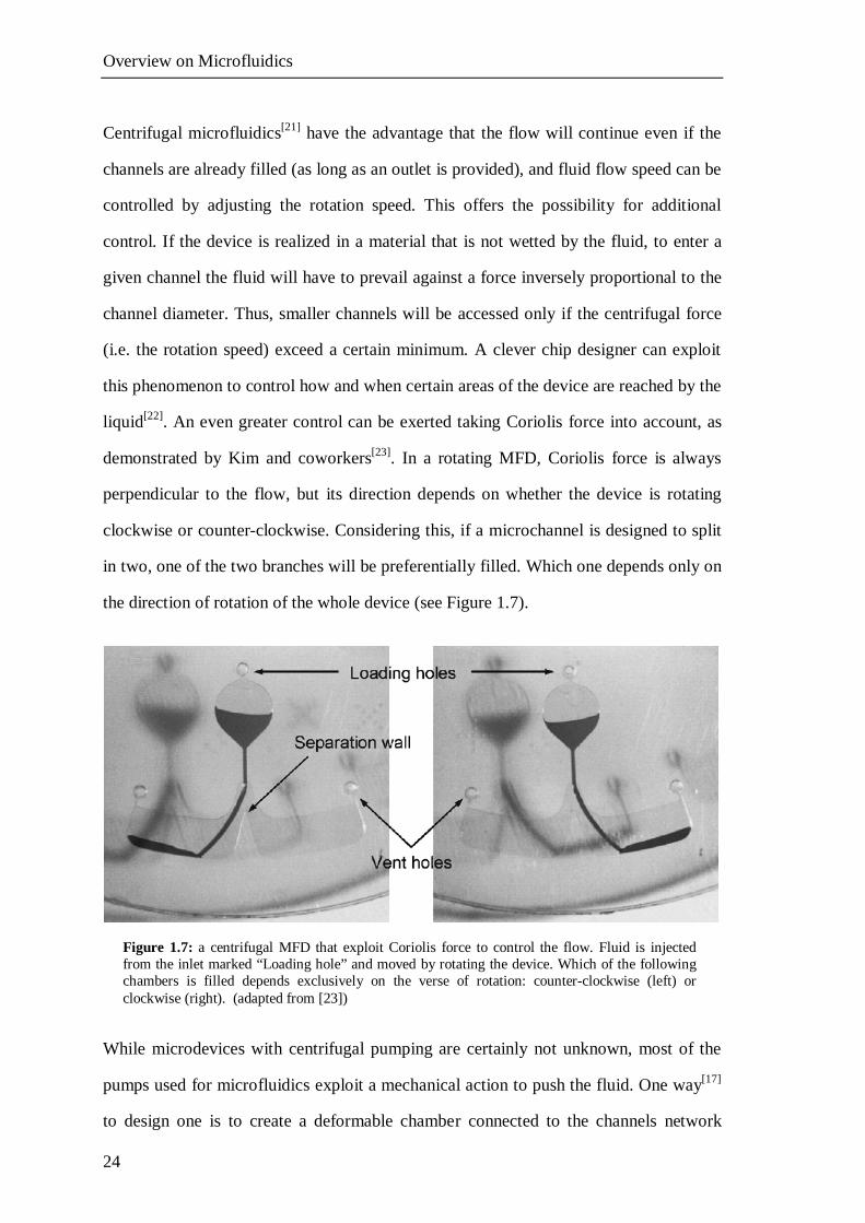
liquid[22]. An even greater control can be exerted taking Coriolis force into account, as
demonstrated by Kim and coworkers[23]. In a rotating MFD, Coriolis force is always
perpendicular to the flow, but its direction depends on whether the device is rotating
clockwise or counter-clockwise. Considering this, if a microchannel is designed to split
in two, one of the two branches will be preferentially filled. Which one depends only on
the direction of rotation of the whole device (see Figure 1.7).
While microdevices with centrifugal pumping are certainly not unknown, most of the
pumps used for microfluidics exploit a mechanical action to push the fluid. One way[17]
to design one is to create a deformable chamber connected to the channels network
Figure 1.7: a centrifugal MFD that exploit Coriolis force to control the flow. Fluid is injected from the inlet marked “Loading hole” and moved by rotating the device. Which of the following chambers is filled depends exclusively on the verse of rotation: counter-clockwise (left) or clockwise (right). (adapted from [23])
Overview on Microfluidics
25
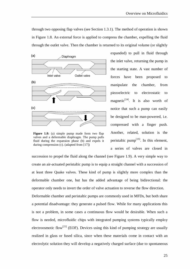
through two opposing flap valves (see Section 1.3.1). The method of operation is shown
in Figure 1.8. An external force is applied to compress the chamber, expelling the fluid
through the outlet valve. Then the chamber is returned to its original volume (or slightly
expanded) to pull in fluid through
the inlet valve, returning the pump in
the starting state. A vast number of
forces have been proposed to
manipulate the chamber, from
piezoelectric to electrostatic to
magnetic[24]. It is also worth of
notice that such a pump can easily
be designed to be man-powered, i.e.
compressed with a finger push.
Another, related, solution is the
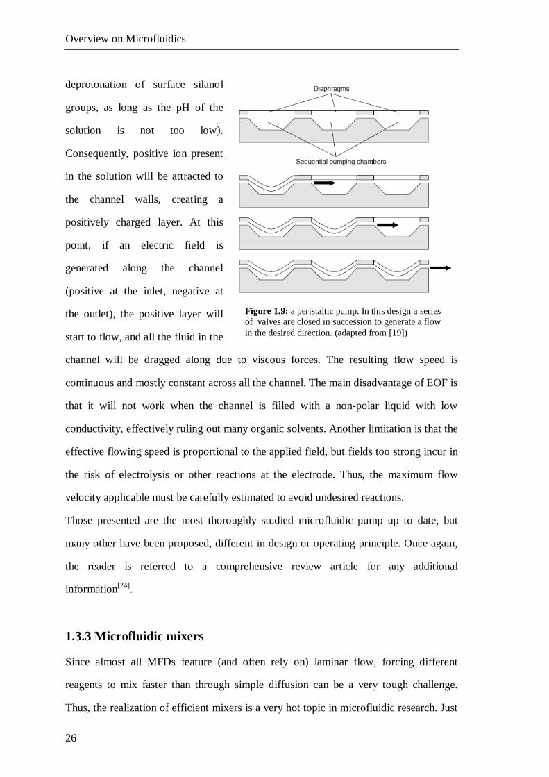
peristaltic pump[19]. In this element,
a series of valves are closed in
succession to propel the fluid along the channel (see Figure 1.9). A very simple way to
create an air-actuated peristaltic pump is to equip a straight channel with a succession of
at least three Quake valves. These kind of pump is slightly more complex than the
deformable chamber one, but has the added advantage of being bidirectional: the
operator only needs to invert the order of valve actuation to reverse the flow direction.
Deformable chamber and peristaltic pumps are commonly used in MFDs, but both share
a potential disadvantage: they generate a pulsed flow. While for many applications this
is not a problem, in some cases a continuous flow would be desirable. When such a
flow is needed, microfluidic chips with integrated pumping systems typically employ
electroosmotic flow[25] (EOF). Devices using this kind of pumping strategy are usually
realized in glass or fused silica, since when these materials come in contact with an
electrolytic solution they will develop a negatively charged surface (due to spontaneous
Figure 1.8: (a) simple pump made form two flap valves and a deformable diaphragm. The pump pulls fluid during the expansion phase (b) and expels it during compression (c). (adapted from [17])
Overview on Microfluidics
26
deprotonation of surface silanol
groups, as long as the pH of the
solution is not too low).
Consequently, positive ion present
in the solution will be attracted to
the channel walls, creating a
positively charged layer. At this
point, if an electric field is
generated along the channel
(positive at the inlet, negative at
the outlet), the positive layer will
start to flow, and all the fluid in the
channel will be dragged along due to viscous forces. The resulting flow speed is
continuous and mostly constant across all the channel. The main disadvantage of EOF is
that it will not work when the channel is filled with a non-polar liquid with low
conductivity, effectively ruling out many organic solvents. Another limitation is that the
effective flowing speed is proportional to the applied field, but fields too strong incur in
the risk of electrolysis or other reactions at the electrode. Thus, the maximum flow
velocity applicable must be carefully estimated to avoid undesired reactions.
Those presented are the most thoroughly studied microfluidic pump up to date, but
many other have been proposed, different in design or operating principle. Once again,
the reader is referred to a comprehensive review article for any additional
information[24].
1.3.3 Microfluidic mixers
Since almost all MFDs feature (and often rely on) laminar flow, forcing different
reagents to mix faster than through simple diffusion can be a very tough challenge.
Thus, the realization of efficient mixers is a very hot topic in microfluidic research. Just
Figure 1.9: a peristaltic pump. In this design a series of valves are closed in succession to generate a flow in the desired direction. (adapted from [19])
Overview on Microfluidics
27
as valves, mixers can be divided in active and passive ones. Active mixers exploit an
external force to achieve mixing, while passive ones work without off-chip intervention.
The most conceptually simple way to mix two fluids is to include inside the channels a
mechanical stirrer (like a paddlewheel). Unfortunately, the tiny dimensions of MFDs
greatly complicate the practical realization of such an element. A micrometric
paddlewheel can be created with any of the various microfabrication techniques (see
Section 1.4), but realizing a miniaturized system able to actually rotate the wheel is a
much more difficult undertaking, one often not worth the effort.
Most active mixers rely instead on inducing perturbation in the laminar flow through
repeated perturbation in the pumping system. As an example, if the relative flow rates
of two fluids flowing together in the same channel is repeatedly varied, mixing between
them is enhanced[26]. Of course, the degree of enhancement is dependant on the nature
and magnitude of the perturbation. Another, usually more efficient solution is to
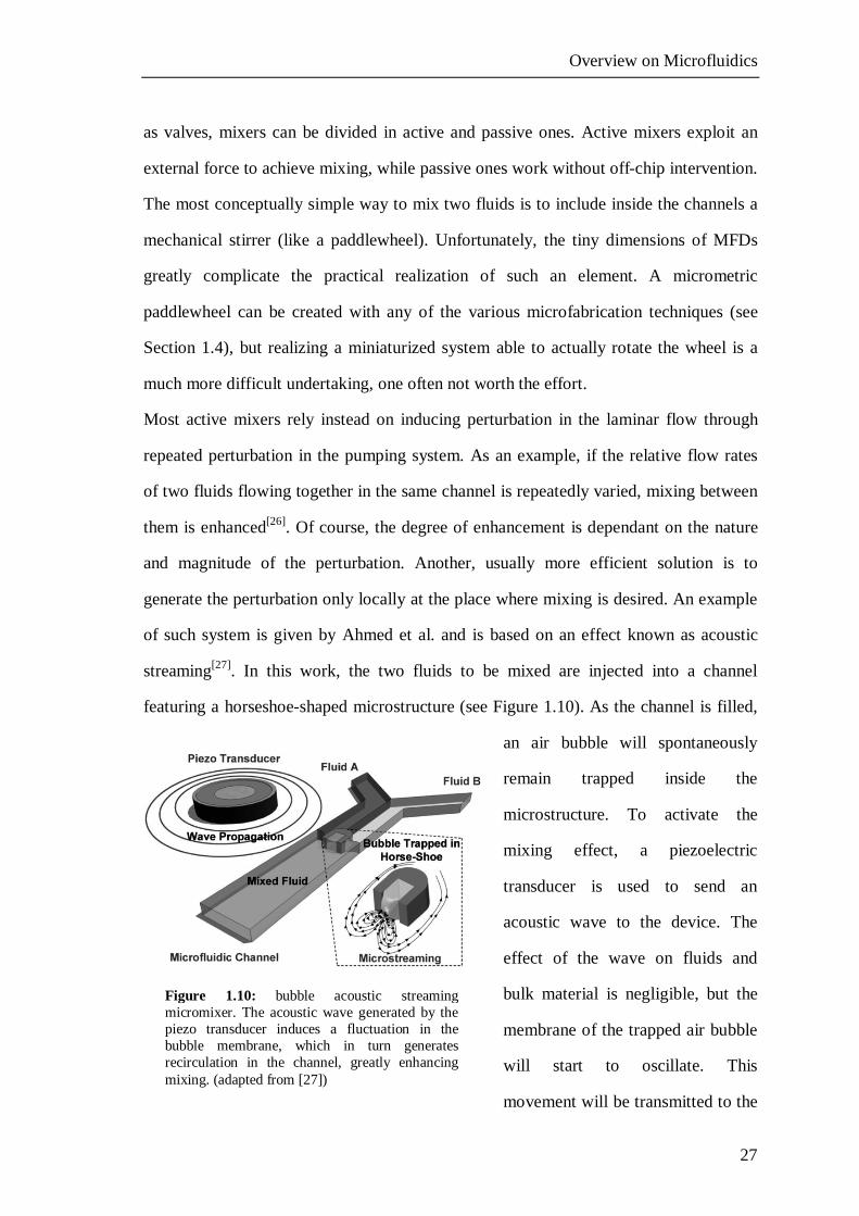
generate the perturbation only locally at the place where mixing is desired. An example
of such system is given by Ahmed et al. and is based on an effect known as acoustic
streaming[27]. In this work, the two fluids to be mixed are injected into a channel
featuring a horseshoe-shaped microstructure (see Figure 1.10). As the channel is filled,
an air bubble will spontaneously
remain trapped inside the
microstructure. To activate the
mixing effect, a piezoelectric
transducer is used to send an
acoustic wave to the device. The
effect of the wave on fluids and
bulk material is negligible, but the
membrane of the trapped air bubble
will start to oscillate. This
movement will be transmitted to the
Figure 1.10: bubble acoustic streaming micromixer. The acoustic wave generated by the piezo transducer induces a fluctuation in the bubble membrane, which in turn generates recirculation in the channel, greatly enhancing mixing. (adapted from [27])
Overview on Microfluidics
28
fluids as fluctuations in velocity and pressure, resulting in strong recirculation and
consequent mixing. The effect can be very intense if the frequency of the acoustic wave
is near the resonance frequency of the bubble. This resonance frequency f depends on
the fluids involved and on the radius of the trapped bubble following[27]:
22 2
1 2 234
f k pa a a
(1.2)
where is the density of the surrounding liquid, is the surface tension, k is the
polytropic exponent of the gas, p is the fluidic pressure and a is the radius of the bubble.
It should be noticed that this equation assumes spherical bubbles, so small differences in
resonance frequency are expected for slightly oblate bubbles such as those trapped in
this device. With this arrangement, mixing across a 240 m wide channel was estimated
to complete within 10 ms.
Active mixers share the advantage that they can be turned on or off as needed,
improving device versatility, but unfortunately all require additional external equipment
(e.g. power sources) limiting portability. Passive mixers, on the other end, are always
“on”, but once fabricated do not require any additional instrumentation. Mostly, passive
microfluidic mixers are based on one of two approach. The first strategy is to reduce the
lateral dimension of the fluid streams so that mixing by diffusion becomes feasible. A
conceptually simple way to obtain this is to divide both inlet streams that have to be
mixed in multiple, much smaller, sub-stream and then recombining them in a single
channel alternating one liquid and the other. The result is a high number of very thin
(few micrometers) streams in which mixing by diffusion can be accomplished in a
matter of seconds[28]. Another possibility is to use two lateral flows to “compress” a
central stream through an effect known as hydrodynamic focusing. As before, once the
stream lateral dimension is so reduced, free diffusion will spontaneously perform the
mixing[29].
A different strategy to obtain mixing is to induce pseudo-turbulent behavior in the flow.
Obstacles, bends and bottlenecks are all viable methods to introduce transversal
Overview on Microfluidics
29
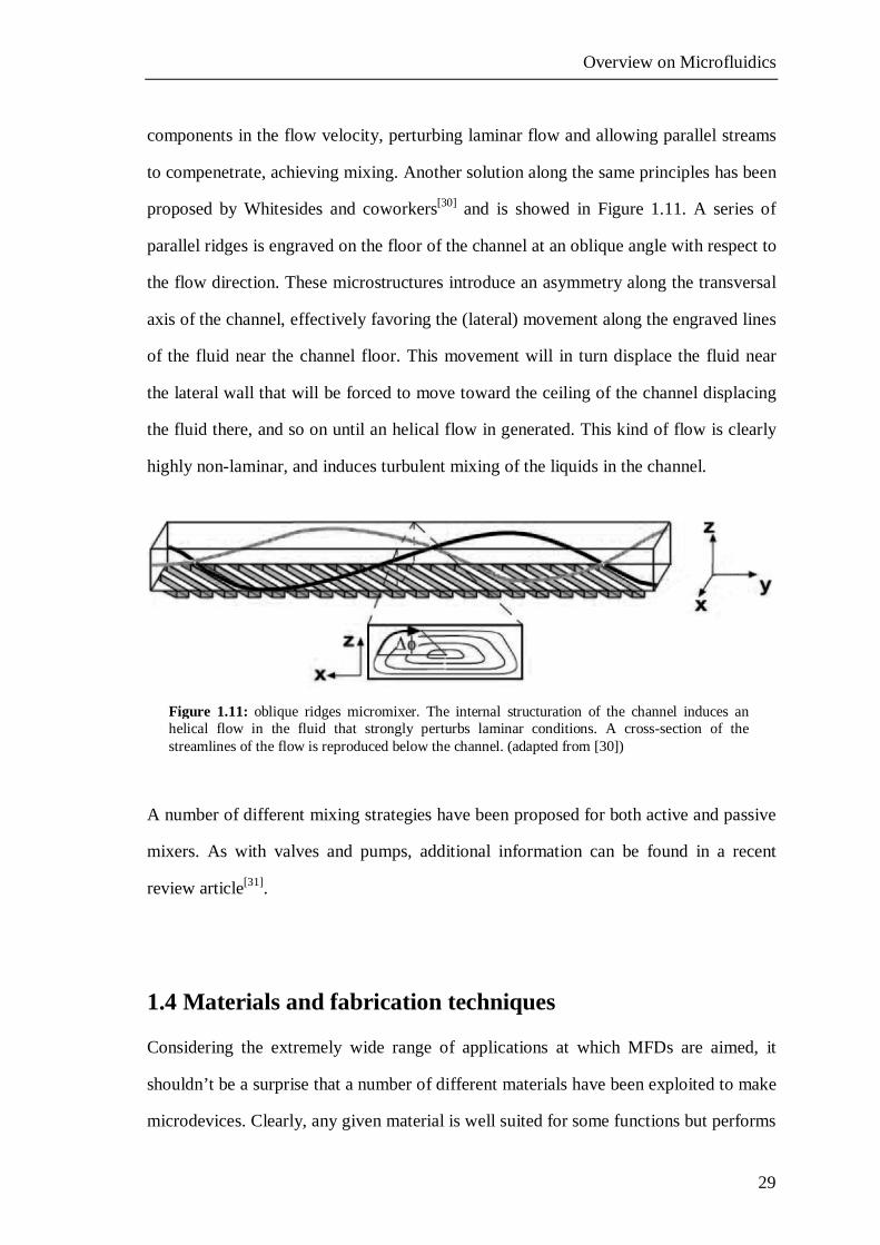
components in the flow velocity, perturbing laminar flow and allowing parallel streams
to compenetrate, achieving mixing. Another solution along the same principles has been
proposed by Whitesides and coworkers[30] and is showed in Figure 1.11. A series of
parallel ridges is engraved on the floor of the channel at an oblique angle with respect to
the flow direction. These microstructures introduce an asymmetry along the transversal
axis of the channel, effectively favoring the (lateral) movement along the engraved lines
of the fluid near the channel floor. This movement will in turn displace the fluid near
the lateral wall that will be forced to move toward the ceiling of the channel displacing
the fluid there, and so on until an helical flow in generated. This kind of flow is clearly
highly non-laminar, and induces turbulent mixing of the liquids in the channel.
A number of different mixing strategies have been proposed for both active and passive
mixers. As with valves and pumps, additional information can be found in a recent
review article[31].
1.4 Materials and fabrication techniques
Considering the extremely wide range of applications at which MFDs are aimed, it
shouldn’t be a surprise that a number of different materials have been exploited to make
microdevices. Clearly, any given material is well suited for some functions but performs
Figure 1.11: oblique ridges micromixer. The internal structuration of the channel induces an helical flow in the fluid that strongly perturbs laminar conditions. A cross-section of the streamlines of the flow is reproduced below the channel. (adapted from [30])
Overview on Microfluidics
30
poorly for others, so different applications require different substrates. Moreover, it is
not unknown (though fairly uncommon) for a single device to be fabricated using two
or more different substances[32,33]. This variety in materials necessarily translates into a
variety of microfabrication techniques that have been established or developed since the
genesis of microfluidics. To report a complete list of materials and techniques would be
quite pointless, but a description of the most common (or interesting) is beyond doubt
useful, and as such will be given in the following.
1.4.1 Hard materials: glass and steel
In ultimate analysis microfluidics originally stems from earlier work on glass
capillaries, so it’s no surprise that glass is one of the most popular MFD material[34–36].
The reason is not only historical, since glass is an excellent substrate for any chemical
application. These MFDs can be filled with almost any chemical without fear of adverse
reaction, and can be heated to high temperature. Additionally, glass is transparent,
making it a good substrate also for optical applications, and is biocompatible, allowing
cells to attach and proliferate on a glass MFD. Apart from being somewhat fragile, glass
has not any real disadvantage as substrate. Its true drawback lies in the fact that glass is
quite difficult to microfabricate or more in general to work with. To answer this
limitation, steel MFDs have been proposed and successfully employed[37,38]. Steel is
chemically resistant to many solvents, able to withstand high temperatures and
pressures and much easier to work than glass. Clearly steel is not transparent, a fact that
rules out (off-chip) optical applications. It is also incompatible with some classes of
reagents (mainly strong acids), and it is not biocompatible, but industrial metal
microfabrication techniques are very well developed. This last fact assures that most
commercial MDFs (especially those for chemical synthesis) are made of steel*.
* See for example the microreactors proposed by Syrris (syrris.com/flow-products) or Flowid (www.flowid.nl/products)
Overview on Microfluidics
31
1.4.2 Soft materials: polymers
While polymers cannot usually compare with glass or steel in terms of mechanical
properties or chemical resistance, these materials are often cheap and much easier to
work with. Interest in polymer MFDs is currently stronger in academic environment
than in industrial facilities, but some commercial plastic MFDs are nonetheless
available on the market[39]. Polymers from microdevices come most often from one of
two categories: photopolymerizable materials and elastomers. Photopolymers, also
called resists, are a well developed class of materials that owes much of its popularity to
microelectronics, since resists are instrumental in the fabrication of microchips. When
used as bulk materials in microfluidics, these substrates allow the fabrication of devices
through photolithography (see Section 1.4.7) without the need for subsequent etching
and resist removal.
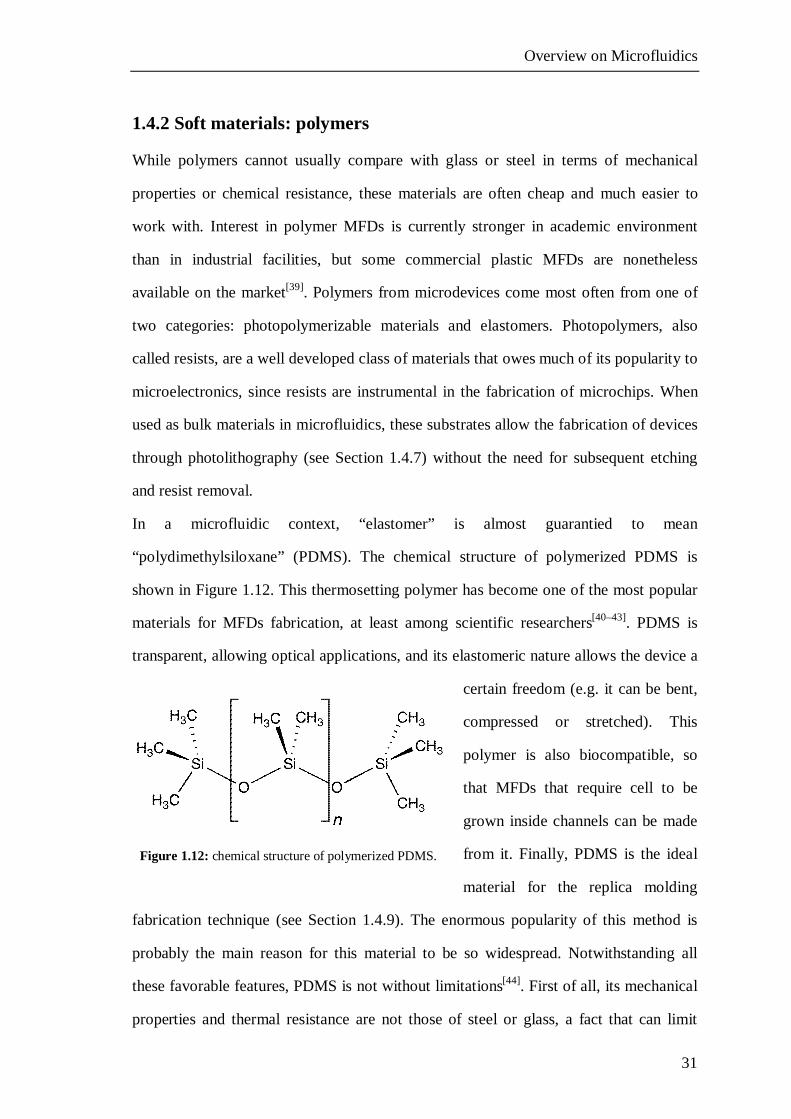
In a microfluidic context, “elastomer” is almost guarantied to mean
“polydimethylsiloxane” (PDMS). The chemical structure of polymerized PDMS is
shown in Figure 1.12. This thermosetting polymer has become one of the most popular
materials for MFDs fabrication, at least among scientific researchers[40–43]. PDMS is
transparent, allowing optical applications, and its elastomeric nature allows the device a
certain freedom (e.g. it can be bent,
compressed or stretched). This
polymer is also biocompatible, so
that MFDs that require cell to be
grown inside channels can be made
from it. Finally, PDMS is the ideal
material for the replica molding
fabrication technique (see Section 1.4.9). The enormous popularity of this method is
probably the main reason for this material to be so widespread. Notwithstanding all
these favorable features, PDMS is not without limitations[44]. First of all, its mechanical
properties and thermal resistance are not those of steel or glass, a fact that can limit
Figure 1.12: chemical structure of polymerized PDMS.
Overview on Microfluidics
32
applications. Particularly problematic are devices that require high pressure, since
(elastomeric) PDMS channels will swell noticeably at pressures far below those
required to actually burst open the device. This polymer is also fairly incompatible with
most organic solvent, since they will be absorbed and eventually lead to material
delamination[45]. Finally, PDMS is permeable to most gasses[46], a fact that can be
regarded as a mixed blessing, since its actual consequences depend on the purpose of
the device: in a cell culturing MFD, oxygen and CO2 permeability ensure that the cells
can survive inside channels. On the other hand the same oxygen can be harmful for
certain chemical reactions with unstable reagents.
1.4.3 Hybrid materials
A sort of middle ground between hard and soft materials is occupied by hybrid
materials, i.e. substrates in which organic and inorganic components coexist. This
peculiar composition confers to these materials hybrid characteristics that share the
advantages of both polymers and harder substances like glass or silica[47]. Typically, the
result will be a substrate with better mechanical properties than pure plastics, but less
brittle and much more workable than ceramics[48]. The blend of organic and inorganic
parts can be made in a number of different ways, the simpler of which is to physically
mix them. As an example, silica nanoparticles dispersed in a polymeric matrix
contribute to increase the elastic modulus of the whole substance[49]. While these
“mixed” materials can surely be used in microfluidic applications, most or the research
work in the field concentrate on materials that are hybrid on the molecular level, that is
whose single molecules share organic and inorganic moieties. Most commonly, these
hybrids present on one end a functional group that can react with other identical
molecules to generate an inorganic Si-O-Si network, and on the other end an organic
moiety. Exactly which organic moiety depends on the application, the rationale being
that while the inorganic network confers mechanical stability to the whole, the organic
half can be used to introduce the desired functionalities in the material. A wide variety
Overview on Microfluidics
33
of different hybrids have been proposed in the literature. As an example, organic
moieties have been used to tune the wettability of the surface[50,51]. Also, the optical
properties of functional organic groups have been exploited for a number of
applications ranging from very simple (e.g. colored glass) to quite complex (e.g.
photochromic materials for optical storage or non-linear absorbers for optical
limiting)[52].
One of the most interesting applications of hybrid materials is to include as organic part
a photopolymerizable moiety. In this case, the material maintains its typical
characteristics (most importantly better mechanical properties than pure polymers), but
also becomes easily patternable via photolithographic methods (see Section 1.4.7),
opening the way for hybrid material microfabrication[53,54].
1.4.4 Micromachining
One of the first developed method for the creation of microdevices is micromachining.
There are several different machines that can engrave a network of channels in a steel or
polymer slab, ranging from CNC (computer numerical control) milling machines to
electrical discharge machining (EDM). All these machines share some features: they are
large and possibly expensive, but very well known to the industry. The greatest
advantage of these techniques is that patterns with arbitrary geometry can be realized
with good precision in an almost completely automated way. Unfortunately, “good”
precision is not always enough. CNC milling on metal can create channels of a few
hundred microns (or down to about 80 m with specifically designed equipment)[55].
EDM (with a machine specifically tuned for micromachining) can achieve resolution
around 100 m or (many) tens of micrometers[56]. If the base material is soft (polymers),
resolution for CNC milling is strongly reduced because of material deformation, while
EDM is downright impossible, since plastics are (usually) nonconductive. Whether
these numbers are good enough or not depends of course on the final application of the
Overview on Microfluidics
34
device, but a number of MFDs require channels dimension on the order of 10
micrometers, ruling out micromachining.
1.4.5 Focused ion beam milling and electron beam lithography
Focused ion beam milling (FIBM) can be considered as the evolution of
micromachining. Instead of removing material from the sample with a rotating cutter, a
focused ion beam is exploited to sputter atoms from the sample surface[57]. The
maximum lateral resolution obtainable depends on the dimension of the focused beam,
which is in principle limited only by the diffraction limit (i.e. about one half of the beam
wavelength). Thanks to the fact that the beam is made of ions, which have an extremely
small wavelength, experimental resolutions down to tens of nanometers have been
reported[57–59]. Depending on the ion energy, some of the ions can be implanted in the
sample. This effect can be beneficial or not, depending on the final application, and can
be controlled by the operator through modulation of the impact energy. FIBM also has
some disadvantage. First of all, it requires complex and expensive instrumentation to
generate, focus and control the required ions. The fact that all the machine must be kept
in (ultra) high vacuum only adds to complexity. Also, this fabrication technique is slow
and serial, thus requiring a long time to realize large structures.
Electron beam lithography (EBL) is very similar to FIBM, with the difference that a
beam of electrons, instead of ions, is employed[60,61]. The result on the sample is
different, since electrons lack the mass to efficiently sputter material. Instead, the
targeted area undergoes a chemical modification that makes it soluble in a suitable
solvent, while the rest of the sample remains unaffected (see Section 1.4.7 for more
examples of lithographic processes). Apart from these differences, EBL shares almost
the same advantages and disadvantages of FIBM, only trading the possibility of ion
implantation for an increased resolution (down to few nanometers). This increase is due
to the fact that while ions can in principle be focalized much tighter (due to their smaller
Overview on Microfluidics
35
wavelength), the sputtering process is less controllable, and often involves all the
neighboring area.
1.4.6 Wet etching and reactive ion etching
Another way of creating MFDs is through chemical (wet) etching. In this technique, the
starting material is partially covered with a mask (typically realized with
photolithography, see Section 1.4.7) featuring holes shaped like the desired channel
network. All the sample is then submerged in an aggressive chemical solution able to
dissolve (etch) the starting material but not the mask. The result is that trenches will be
created in the bulk material corresponding to the mask holes geometry[62]. This method
is simple, and its resolution is in principle only limited by that of the mask.
Unfortunately, etching is an isotropic process. This means that once the very first layer
of material is removed, the etching process will proceed in every direction, including
under the mask. The result will be rounded channels with internal diameters greater than
the mask dimensions (decreased resolution). Notwithstanding this limitation, wet
etching is a much favored technique, especially when the required channels are not too
deep. When high resolution or deep channels are required, a modified etching technique
can be used. Reactive ion etching (RIE) works along similar principles, but instead of a
chemical solution, a plasma of positive reactive ions is employed[63]. This plasma is
subjected to an electrical field perpendicular to the sample surface that forces the ions to
move towards the (mask covered) sample. Where the ions impact, sample material is
removed both through a sputtering effect and due to the chemical reactivity of the
plasma. The presence of the electric field introduces a strong anisotropicity to the
process, ensuring that lateral etching is much slower than vertical one. Thus, deep
channel with mask-limited resolution can be obtained.
Both kind of etching are commonly used to create MFDs, especially those made of
materials difficult to work otherwise, like glass. This technique has the great advantage
of being able to work large areas at the same time, allowing the realization of large
Overview on Microfluidics
36
devices. Wet etching is also quite simple and cheap, since the most expensive
component is usually the mask, which can often be reused many times. With RIE, the
instrumentation is a bit more expensive, since it must include a reaction chamber kept in
low vacuum, and while the masks are almost immune to chemical etch from the plasma,
the sputtering process damages them, compelling the user to replace them after a few
cycles.
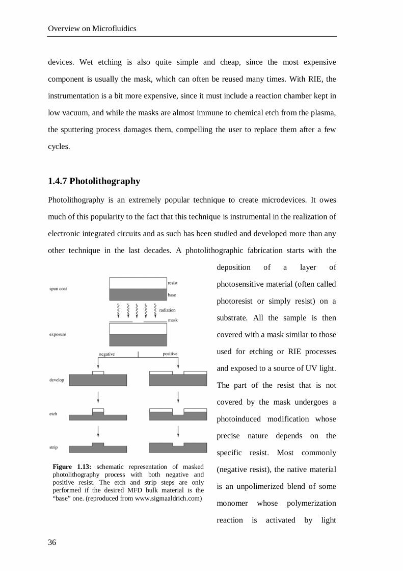
1.4.7 Photolithography
Photolithography is an extremely popular technique to create microdevices. It owes
much of this popularity to the fact that this technique is instrumental in the realization of
electronic integrated circuits and as such has been studied and developed more than any
other technique in the last decades. A photolithographic fabrication starts with the
deposition of a layer of
photosensitive material (often called
photoresist or simply resist) on a
substrate. All the sample is then
covered with a mask similar to those
used for etching or RIE processes
and exposed to a source of UV light.
The part of the resist that is not
covered by the mask undergoes a
photoinduced modification whose
precise nature depends on the
specific resist. Most commonly
(negative resist), the native material
is an unpolimerized blend of some
monomer whose polymerization
reaction is activated by light
Figure 1.13: schematic representation of masked photolithography process with both negative and positive resist. The etch and strip steps are only performed if the desired MFD bulk material is the “base” one. (reproduced from www.sigmaaldrich.com)
Overview on Microfluidics
37
absorption. If this is the case, the exposed material undergoes crosslinking and becomes
resistant to a number of solvents able to dissolve the monomer form. The unpolimerized
resist is then removed with said solvents (a process known as development) to obtain
the desired microstructures. In other resists (positive resist), the material is already
crosslinked and UV light actually breaks down the connection between monomers. If
this is the case, the selected solvent will wash the exposed material, while that under the
mask will be unaffected. Both these processes are exemplified in Figure 1.13.
Regardless of what kind of resist is used, the result will be a microstructure supported
on a substrate that feature a positive or negative reproduction of the mask. This
microstructure could be the desired device, or in other cases the substrate is the material
of interest and the polymer structure is just the mask for the following etching process.
Photolithography is a very well developed technique, quite simple in principle but with
some limitations. First of all, the resolution of the final structure is limited by that of the
mask, which must be created by other methods. However, such masks are only
subjected to light exposure and not to aggressive chemicals, so each mask can be used
indefinitely. Also, if the final device does not require resolutions exceeding a few
hundred micrometers, masks can be created very cheaply by printing them in black ink
on a transparent sheet[40]. Even if the mask is exceptionally resolved, the use of light
imposes a further limitation on the maximum resolution (diffraction limit). Since the
smallest feature obtainable is proportional to the wavelength of the radiation used, many
attempt have been made to develop a photolithographic process that exploits light with
shorter wavelength (deep UV or X-rays). With these techniques structures smaller than
100 nm have been created[64], but the difficulty in handling photons so energetic poses a
strong limitation to the diffusion of this processes.
1.4.8 Direct laser writing
Direct laser writing (DLW) is the natural evolution of masked photolithography. Instead
of using a mask and a wide light source, a laser beam is focalized on the sample and
Overview on Microfluidics
38
moved to directly write the desired pattern in point-by-point fashion. The greatest
advantage of this technique is that there is no longer need for a mask. This fact greatly
simplifies the process, since it eliminates all the mask microfabrication steps that can be
quite challenging for masks featuring complex patterns. The resolution of DLW is in
principle equal to the smallest focal radius obtainable (i.e. the diffraction limit) but in
practice lens aberrations and other hidden processes (e.g. polymerization propagation
outside the actually exposed area) mean that the smallest feature obtainable is on the
order of some micrometer (with soft UV light, that is wavelengths around 350-400 nm).
The greatest drawback of this technique is that, being serial, it can take quite a long time
to produce large patterns. However, with high laser powers the writing speed can be
quite high (some millimeter per second or even more) and the process is easily
automated, meaning that this is more a drawback for laboratory research than for
industrial application.
A further evolution of DLW is the use of two-photon absorption processes to induce
resist polymerization. Two-photon absorption is a process in which a molecule, instead
of absorbing a photon of the appropriate energy to make a transition, absorbs two
photon each of half the required energy to obtain the same result[65]. These kind of
transitions are much less probable than classic, one-photon ones, so this process has two
requirements. First of all, the number of photons impacting on the sample must be high
(to account for small interaction probability), which means high light intensity.
Secondly, linear (one-photon) absorption processes must be absent at the selected
wavelength or, being much more probable, they will completely drown non-linear ones.
In practice, for common UV-photoresist that absorb linearly at wavelength around 400
nm, the selected exposure wavelength will be around 800 nm, where the resist does not
absorb through one-photon processes but only via two-photon absorption. The
advantage in using non-linear processes is that the efficiency of two-photon absorption
and subsequent resist polymerization is strongly (quadratically) dependant on the light
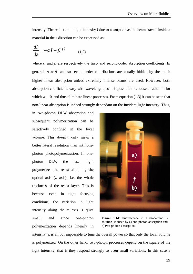
Overview on Microfluidics
39
intensity. The reduction in light intensity I due to absorption as the beam travels inside a
material in the z direction can be expressed as:
2dI I Idz
(1.3)
where and are respectively the first- and second-order absorption coefficients. In
general, and so second-order contributions are usually hidden by the much
higher linear absorption unless extremely intense beams are used. However, both
absorption coefficients vary with wavelength, so it is possible to choose a radiation for
which 0 and thus eliminate linear processes. From equation (1.3) it can be seen that
non-linear absorption is indeed strongly dependant on the incident light intensity. Thus,
in two-photon DLW absorption and
subsequent polymerization can be
selectively confined in the focal
volume. This doesn’t only mean a
better lateral resolution than with one-
photon photopolymerization. In one-
photon DLW the laser light
polymerizes the resist all along the
optical axis (z axis), i.e. the whole
thickness of the resist layer. This is
because even in tight focusing
conditions, the variation in light
intensity along the z axis is quite
small, and since one-photon
polymerization depends linearly in
intensity, it is all but impossible to tune the overall power so that only the focal volume
is polymerized. On the other hand, two-photon processes depend on the square of the
light intensity, that is they respond strongly to even small variations. In this case a
Figure 1.14: fluorescence in a rhodamine B solution induced by a) one-photon absorption and b) two-photon absorption.
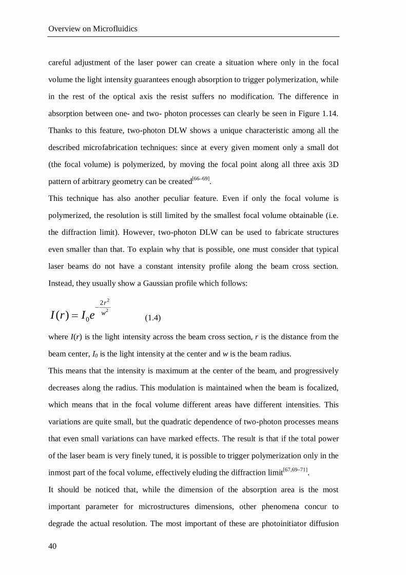
Overview on Microfluidics
40
careful adjustment of the laser power can create a situation where only in the focal
volume the light intensity guarantees enough absorption to trigger polymerization, while
in the rest of the optical axis the resist suffers no modification. The difference in
absorption between one- and two- photon processes can clearly be seen in Figure 1.14.
Thanks to this feature, two-photon DLW shows a unique characteristic among all the
described microfabrication techniques: since at every given moment only a small dot
(the focal volume) is polymerized, by moving the focal point along all three axis 3D
pattern of arbitrary geometry can be created[66–69].
This technique has also another peculiar feature. Even if only the focal volume is
polymerized, the resolution is still limited by the smallest focal volume obtainable (i.e.
the diffraction limit). However, two-photon DLW can be used to fabricate structures
even smaller than that. To explain why that is possible, one must consider that typical
laser beams do not have a constant intensity profile along the beam cross section.
Instead, they usually show a Gaussian profile which follows:
2
22
0( )r
wI r I e
(1.4)
where I(r) is the light intensity across the beam cross section, r is the distance from the
beam center, I0 is the light intensity at the center and w is the beam radius.
This means that the intensity is maximum at the center of the beam, and progressively
decreases along the radius. This modulation is maintained when the beam is focalized,
which means that in the focal volume different areas have different intensities. This
variations are quite small, but the quadratic dependence of two-photon processes means
that even small variations can have marked effects. The result is that if the total power
of the laser beam is very finely tuned, it is possible to trigger polymerization only in the
inmost part of the focal volume, effectively eluding the diffraction limit[67,69–71].
It should be noticed that, while the dimension of the absorption area is the most
important parameter for microstructures dimensions, other phenomena concur to
degrade the actual resolution. The most important of these are photoinitiator diffusion
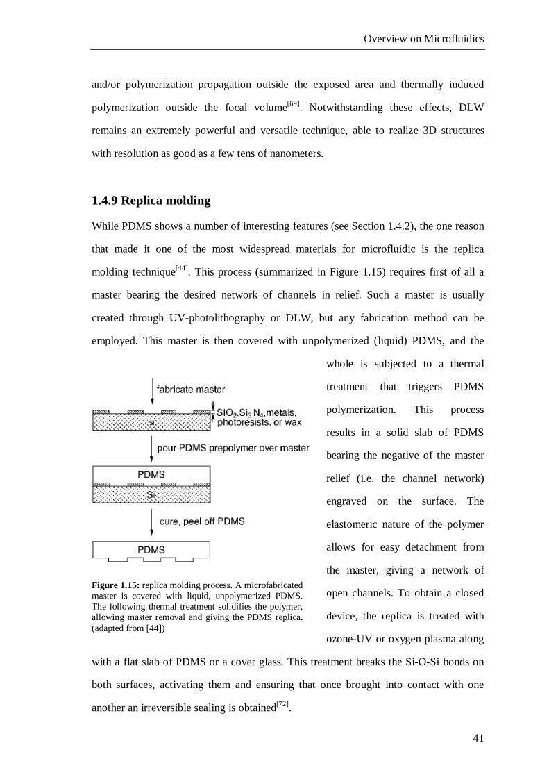
Overview on Microfluidics
41
and/or polymerization propagation outside the exposed area and thermally induced
polymerization outside the focal volume[69]. Notwithstanding these effects, DLW
remains an extremely powerful and versatile technique, able to realize 3D structures
with resolution as good as a few tens of nanometers.
1.4.9 Replica molding
While PDMS shows a number of interesting features (see Section 1.4.2), the one reason
that made it one of the most widespread materials for microfluidic is the replica
molding technique[44]. This process (summarized in Figure 1.15) requires first of all a
master bearing the desired network of channels in relief. Such a master is usually
created through UV-photolithography or DLW, but any fabrication method can be
employed. This master is then covered with unpolymerized (liquid) PDMS, and the
whole is subjected to a thermal
treatment that triggers PDMS
polymerization. This process
results in a solid slab of PDMS
bearing the negative of the master
relief (i.e. the channel network)
engraved on the surface. The
elastomeric nature of the polymer
allows for easy detachment from
the master, giving a network of
open channels. To obtain a closed
device, the replica is treated with
ozone-UV or oxygen plasma along
with a flat slab of PDMS or a cover glass. This treatment breaks the Si-O-Si bonds on
both surfaces, activating them and ensuring that once brought into contact with one
another an irreversible sealing is obtained[72].
Figure 1.15: replica molding process. A microfabricated master is covered with liquid, unpolymerized PDMS. The following thermal treatment solidifies the polymer, allowing master removal and giving the PDMS replica. (adapted from [44])
Overview on Microfluidics
42
This fabrication technique is fast and very cheap, since a single master can be used to
generate a great number of replicas. The fact that PDMS is an elastomer allows the
replica of complex structures where a stiffer material would break while being detached
from the master. The greatest limitation to replica molding versatility is that it cannot
replicate most three-dimensional structures. If the 3D part is limited to some
overhanging feature, replica molding can still (in some cases) be employed, one again
thanks to the elastomeric nature of PDMS that allows the replica to bend or stretch as
needed to break free from the master[73]. However, structures with closed loops are
completely off-limits, since there would be no way to separate the master from the
PDMS, unless a master is sacrificed for every replica.
1.5 Optofluidics
Originally, the field of microfluidics concerned itself only with fluids. However, a great
number of chemical reactions and characterization techniques are enhanced by the
suitable application of light, so many researcher have explored the possibility of
including optical elements inside MFDs. This new field, dubbed “optofluidics”, has
given rise to a high number of publications in the last few years[74–76]. The main aims of
optofluidic devices and a selection of proposed optical elements are reported in the
following.
1.5.1 Photochemistry in microchannels
The most straightforward way to include light inside MFDs is simply to expose the
entire device to an appropriate source of radiation. This approach is the natural
evolution of batch (macroscale) photochemistry which is commonly used in chemical
synthesis to obtain greater yields or selectivity. Once again, the use of microfluidic
channels can enhance the performances of such devices[77]. One of the greatest
limitation of macroscale apparatuses for photochemistry is that the radiation is
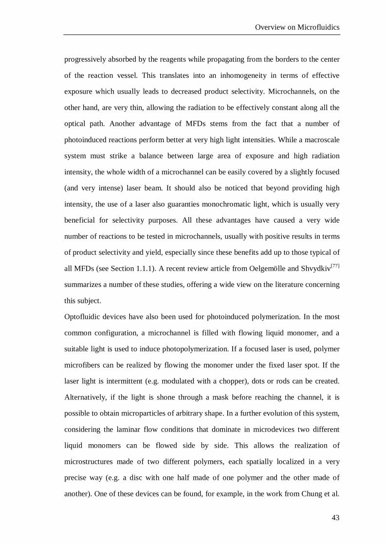
Overview on Microfluidics
43
progressively absorbed by the reagents while propagating from the borders to the center
of the reaction vessel. This translates into an inhomogeneity in terms of effective
exposure which usually leads to decreased product selectivity. Microchannels, on the
other hand, are very thin, allowing the radiation to be effectively constant along all the
optical path. Another advantage of MFDs stems from the fact that a number of
photoinduced reactions perform better at very high light intensities. While a macroscale
system must strike a balance between large area of exposure and high radiation
intensity, the whole width of a microchannel can be easily covered by a slightly focused
(and very intense) laser beam. It should also be noticed that beyond providing high
intensity, the use of a laser also guaranties monochromatic light, which is usually very
beneficial for selectivity purposes. All these advantages have caused a very wide
number of reactions to be tested in microchannels, usually with positive results in terms
of product selectivity and yield, especially since these benefits add up to those typical of
all MFDs (see Section 1.1.1). A recent review article from Oelgemölle and Shvydkiv[77]
summarizes a number of these studies, offering a wide view on the literature concerning
this subject.
Optofluidic devices have also been used for photoinduced polymerization. In the most
common configuration, a microchannel is filled with flowing liquid monomer, and a
suitable light is used to induce photopolymerization. If a focused laser is used, polymer
microfibers can be realized by flowing the monomer under the fixed laser spot. If the
laser light is intermittent (e.g. modulated with a chopper), dots or rods can be created.
Alternatively, if the light is shone through a mask before reaching the channel, it is
possible to obtain microparticles of arbitrary shape. In a further evolution of this system,
considering the laminar flow conditions that dominate in microdevices two different
liquid monomers can be flowed side by side. This allows the realization of
microstructures made of two different polymers, each spatially localized in a very
precise way (e.g. a disc with one half made of one polymer and the other made of
another). One of these devices can be found, for example, in the work from Chung et al.
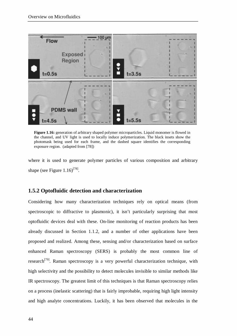
Overview on Microfluidics
44
where it is used to generate polymer particles of various composition and arbitrary
shape (see Figure 1.16)[78].
1.5.2 Optofluidic detection and characterization
Considering how many characterization techniques rely on optical means (from
spectroscopic to diffractive to plasmonic), it isn’t particularly surprising that most
optofluidic devices deal with these. On-line monitoring of reaction products has been
already discussed in Section 1.1.2, and a number of other applications have been
proposed and realized. Among these, sensing and/or characterization based on surface
enhanced Raman spectroscopy (SERS) is probably the most common line of
research[79]. Raman spectroscopy is a very powerful characterization technique, with
high selectivity and the possibility to detect molecules invisible to similar methods like
IR spectroscopy. The greatest limit of this techniques is that Raman spectroscopy relies
on a process (inelastic scattering) that is fairly improbable, requiring high light intensity
and high analyte concentrations. Luckily, it has been observed that molecules in the
Figure 1.16: generation of arbitrary shaped polymer microparticles. Liquid monomer is flowed in the channel, and UV light is used to locally induce polymerization. The black insets show the photomask being used for each frame, and the dashed square identifies the corresponding exposure region. (adapted from [78])
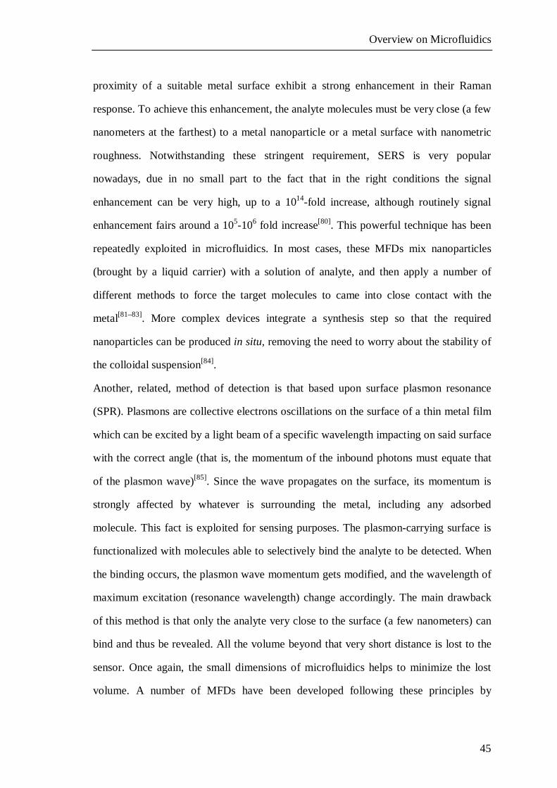
Overview on Microfluidics
45
proximity of a suitable metal surface exhibit a strong enhancement in their Raman
response. To achieve this enhancement, the analyte molecules must be very close (a few
nanometers at the farthest) to a metal nanoparticle or a metal surface with nanometric
roughness. Notwithstanding these stringent requirement, SERS is very popular
nowadays, due in no small part to the fact that in the right conditions the signal
enhancement can be very high, up to a 1014-fold increase, although routinely signal
enhancement fairs around a 105-106 fold increase[80]. This powerful technique has been
repeatedly exploited in microfluidics. In most cases, these MFDs mix nanoparticles
(brought by a liquid carrier) with a solution of analyte, and then apply a number of
different methods to force the target molecules to came into close contact with the
metal[81–83]. More complex devices integrate a synthesis step so that the required
nanoparticles can be produced in situ, removing the need to worry about the stability of
the colloidal suspension[84].
Another, related, method of detection is that based upon surface plasmon resonance
(SPR). Plasmons are collective electrons oscillations on the surface of a thin metal film
which can be excited by a light beam of a specific wavelength impacting on said surface
with the correct angle (that is, the momentum of the inbound photons must equate that
of the plasmon wave)[85]. Since the wave propagates on the surface, its momentum is
strongly affected by whatever is surrounding the metal, including any adsorbed
molecule. This fact is exploited for sensing purposes. The plasmon-carrying surface is
functionalized with molecules able to selectively bind the analyte to be detected. When
the binding occurs, the plasmon wave momentum gets modified, and the wavelength of
maximum excitation (resonance wavelength) change accordingly. The main drawback
of this method is that only the analyte very close to the surface (a few nanometers) can
bind and thus be revealed. All the volume beyond that very short distance is lost to the
sensor. Once again, the small dimensions of microfluidics helps to minimize the lost
volume. A number of MFDs have been developed following these principles by
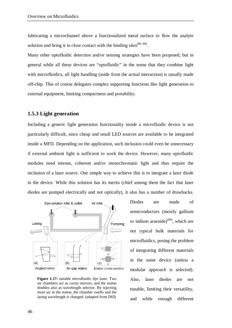
Overview on Microfluidics
46
fabricating a microchannel above a functionalized metal surface to flow the analyte
solution and bring it in close contact with the binding sites[86–88].
Many other optofluidic detection and/or sensing strategies have been proposed, but in
general while all these devices are “optofluidic” in the sense that they combine light
with microfluidics, all light handling (aside from the actual interaction) is usually made
off-chip. This of course delegates complex supporting functions like light generation to
external equipment, limiting compactness and portability.
1.5.3 Light generation
Including a generic light generation functionality inside a microfluidic device is not
particularly difficult, since cheap and small LED sources are available to be integrated
inside a MFD. Depending on the application, such inclusion could even be unnecessary
if external ambient light is sufficient to work the device. However, many optofluidic
modules need intense, coherent and/or monochromatic light and thus require the
inclusion of a laser source. One simple way to achieve this is to integrate a laser diode
in the device. While this solution has its merits (chief among them the fact that laser
diodes are pumped electrically and not optically), it also has a number of drawbacks.
Diodes are made of
semiconductors (mostly gallium
or indium arsenide)[89], which are
not typical bulk materials for
microfluidics, posing the problem
of integrating different materials
in the same device (unless a
modular approach is selected).
Also, laser diodes are not
tunable, limiting their versatility,
and while enough different
Figure 1.17: tunable microfluidic dye laser. Two air chambers act as cavity mirrors, and the etalon doubles also as wavelength selector. By injecting more air in the etalon, the chamber swells and the lasing wavelength is changed. (adapted from [90])
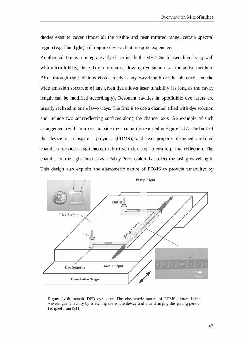
Overview on Microfluidics
47
diodes exist to cover almost all the visible and near infrared range, certain spectral
region (e.g. blue light) still require devices that are quite expensive.
Another solution is to integrate a dye laser inside the MFD. Such lasers blend very well
with microfluidics, since they rely upon a flowing dye solution as the active medium.
Also, through the judicious choice of dyes any wavelength can be obtained, and the
wide emission spectrum of any given dye allows laser tunability (as long as the cavity
length can be modified accordingly). Resonant cavities in optofluidic dye lasers are
usually realized in one of two ways. The first is to use a channel filled with dye solution
and include two semireflecting surfaces along the channel axis. An example of such
arrangement (with “mirrors” outside the channel) is reported in Figure 1.17. The bulk of
the device is transparent polymer (PDMS), and two properly designed air-filled
chambers provide a high enough refractive index step to ensure partial reflection. The
chamber on the right doubles as a Fabry-Perot etalon that select the lasing wavelength.
This design also exploits the elastomeric nature of PDMS to provide tunability: by
Figure 1.18: tunable DFB dye laser. The elastomeric nature of PDMS allows lasing wavelength tunability by stretching the whole device and thus changing the grating period. (adapted from [91])
Overview on Microfluidics
48
forcing more air in the etalon chamber, the increased pressure causes the chamber to
swell, effectively changing the length of the etalon and thus the lasing wavelength. With
this arrangement, the authors reported a tunability range of 14 nm centered at 588
nm[90].
The second possibility is to realize a distributed feedback (DFB) laser by fabricating
pillars inside the dye channel to generate the periodic refractive index modulation
needed to confine and amplify light. Figure 1.18 shows the scheme of such a device[91].
Once again it is realized in PDMS, and as in the previous example, the elasticity of this
material is exploited to achieve tunability. In this case, the whole device is mechanically
stretched to modify the period of the refractive index modulation and consequently
change the lasing wavelength. Using a combination of two dyes as the gain medium, the
authors reported a 60 nm modulation of the emission with a 5% stretching of the device.
It is worth of notice that the elasticity of PDMS is such that the limiting factor in lasing
tunability is the emission spectrum of the selected dyes and not, as could be expected,
the maximum deformation achievable by the material.
1.5.4 Light guiding
Regardless of whether the light is generated on- or off-chip, to be used for the desired
application it must be guided to a specific location inside the device. For the simplest
MFDs, simply pointing the beam from the source towards said location is enough. More
complex devices might require additional care, especially if the target location is
beneath layers of materials that could reflect, refract or scatter the light. The issue is
even more sensitive if the light must not be brought to, but collected from said location
and conveyed to (for example) a detector. The typical situation of this kind would be
weak, highly divergent light emitted from some point inside the device that must be
guided somewhere else. The only way to do this efficiently is to employ waveguides.
Conventional optical waveguides (silica fibers) can be integrated in a MFD, or the bulk
material of the device can be locally modified to increase its refractive index, allowing
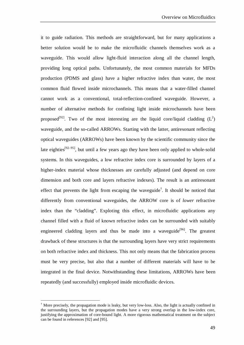
Overview on Microfluidics
49
it to guide radiation. This methods are straightforward, but for many applications a
better solution would be to make the microfluidic channels themselves work as a
waveguide. This would allow light-fluid interaction along all the channel length,
providing long optical paths. Unfortunately, the most common materials for MFDs
production (PDMS and glass) have a higher refractive index than water, the most
common fluid flowed inside microchannels. This means that a water-filled channel
cannot work as a conventional, total-reflection-confined waveguide. However, a
number of alternative methods for confining light inside microchannels have been
proposed[92]. Two of the most interesting are the liquid core/liquid cladding (L2)
waveguide, and the so-called ARROWs. Starting with the latter, antiresonant reflecting
optical waveguides (ARROWs) have been known by the scientific community since the
late eighties[92–95], but until a few years ago they have been only applied to whole-solid
systems. In this waveguides, a low refractive index core is surrounded by layers of a
higher-index material whose thicknesses are carefully adjusted (and depend on core
dimension and both core and layers refractive indexes). The result is an antiresonant
effect that prevents the light from escaping the waveguide†. It should be noticed that
differently from conventional waveguides, the ARROW core is of lower refractive
index than the “cladding”. Exploting this effect, in microfluidic applications any
channel filled with a fluid of known refractive index can be surrounded with suitably
engineered cladding layers and thus be made into a waveguide[96]. The greatest
drawback of these structures is that the surrounding layers have very strict requirements
on both refractive index and thickness. This not only means that the fabrication process
must be very precise, but also that a number of different materials will have to be
integrated in the final device. Notwithstanding these limitations, ARROWs have been
repeatedly (and successfully) employed inside microfluidic devices.
† More precisely, the propagation mode is leaky, but very low-loss. Also, the light is actually confined in the surrounding layers, but the propagation modes have a very strong overlap in the low-index core, justifying the approximation of core-bound light. A more rigorous mathematical treatment on the subject can be found in references [92] and [95].
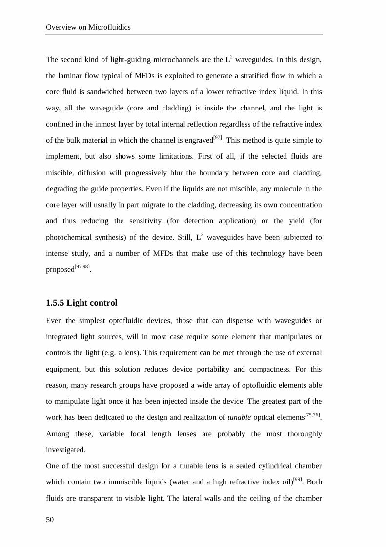
Overview on Microfluidics
50
The second kind of light-guiding microchannels are the L2 waveguides. In this design,
the laminar flow typical of MFDs is exploited to generate a stratified flow in which a
core fluid is sandwiched between two layers of a lower refractive index liquid. In this
way, all the waveguide (core and cladding) is inside the channel, and the light is
confined in the inmost layer by total internal reflection regardless of the refractive index
of the bulk material in which the channel is engraved[97]. This method is quite simple to
implement, but also shows some limitations. First of all, if the selected fluids are
miscible, diffusion will progressively blur the boundary between core and cladding,
degrading the guide properties. Even if the liquids are not miscible, any molecule in the
core layer will usually in part migrate to the cladding, decreasing its own concentration
and thus reducing the sensitivity (for detection application) or the yield (for
photochemical synthesis) of the device. Still, L2 waveguides have been subjected to
intense study, and a number of MFDs that make use of this technology have been
proposed[97,98].
1.5.5 Light control
Even the simplest optofluidic devices, those that can dispense with waveguides or
integrated light sources, will in most case require some element that manipulates or
controls the light (e.g. a lens). This requirement can be met through the use of external
equipment, but this solution reduces device portability and compactness. For this
reason, many research groups have proposed a wide array of optofluidic elements able
to manipulate light once it has been injected inside the device. The greatest part of the
work has been dedicated to the design and realization of tunable optical elements[75,76].
Among these, variable focal length lenses are probably the most thoroughly
investigated.
One of the most successful design for a tunable lens is a sealed cylindrical chamber
which contain two immiscible liquids (water and a high refractive index oil)[99]. Both
fluids are transparent to visible light. The lateral walls and the ceiling of the chamber
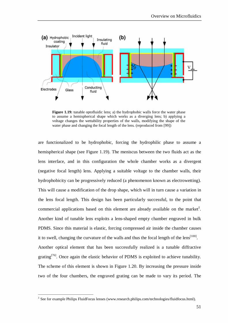
Overview on Microfluidics
51
are functionalized to be hydrophobic, forcing the hydrophilic phase to assume a
hemispherical shape (see Figure 1.19). The meniscus between the two fluids act as the
lens interface, and in this configuration the whole chamber works as a divergent
(negative focal length) lens. Applying a suitable voltage to the chamber walls, their
hydrophobicity can be progressively reduced (a phenomenon known as electrowetting).
This will cause a modification of the drop shape, which will in turn cause a variation in
the lens focal length. This design has been particularly successful, to the point that
commercial applications based on this element are already available on the market‡.
Another kind of tunable lens exploits a lens-shaped empty chamber engraved in bulk
PDMS. Since this material is elastic, forcing compressed air inside the chamber causes
it to swell, changing the curvature of the walls and thus the focal length of the lens[100].
Another optical element that has been successfully realized is a tunable diffractive
grating[76]. Once again the elastic behavior of PDMS is exploited to achieve tunability.
The scheme of this element is shown in Figure 1.20. By increasing the pressure inside
two of the four chambers, the engraved grating can be made to vary its period. The
‡ See for example Philips FluidFocus lenses (www.research.philips.com/technologies/fluidfocus.html).
Figure 1.19: tunable optofluidic lens; a) the hydrophobic walls force the water phase to assume a hemispherical shape which works as a diverging lens; b) applying a voltage changes the wettability properties of the walls, modifying the shape of the water phase and changing the focal length of the lens. (reproduced from [99])
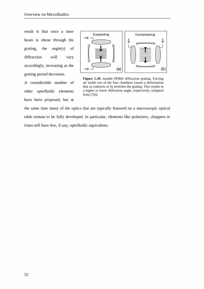
Overview on Microfluidics
52
result is that once a laser
beam is shone through the
grating, the angle(s) of
diffraction will vary
accordingly, increasing as the
grating period decreases.
A considerable number of
other optofluidic elements
have been proposed, but at
the same time many of the optics that are typically featured on a macroscopic optical
table remain to be fully developed. In particular, elements like polarizers, choppers or
irises still have few, if any, optofluidic equivalents.
Figure 1.20: tunable PDMS diffraction grating. Forcing air inside two of the four chambers causes a deformation that a) contracts or b) stretches the grating. This results in a higher or lower diffraction angle, respectively. (adapted from [76])
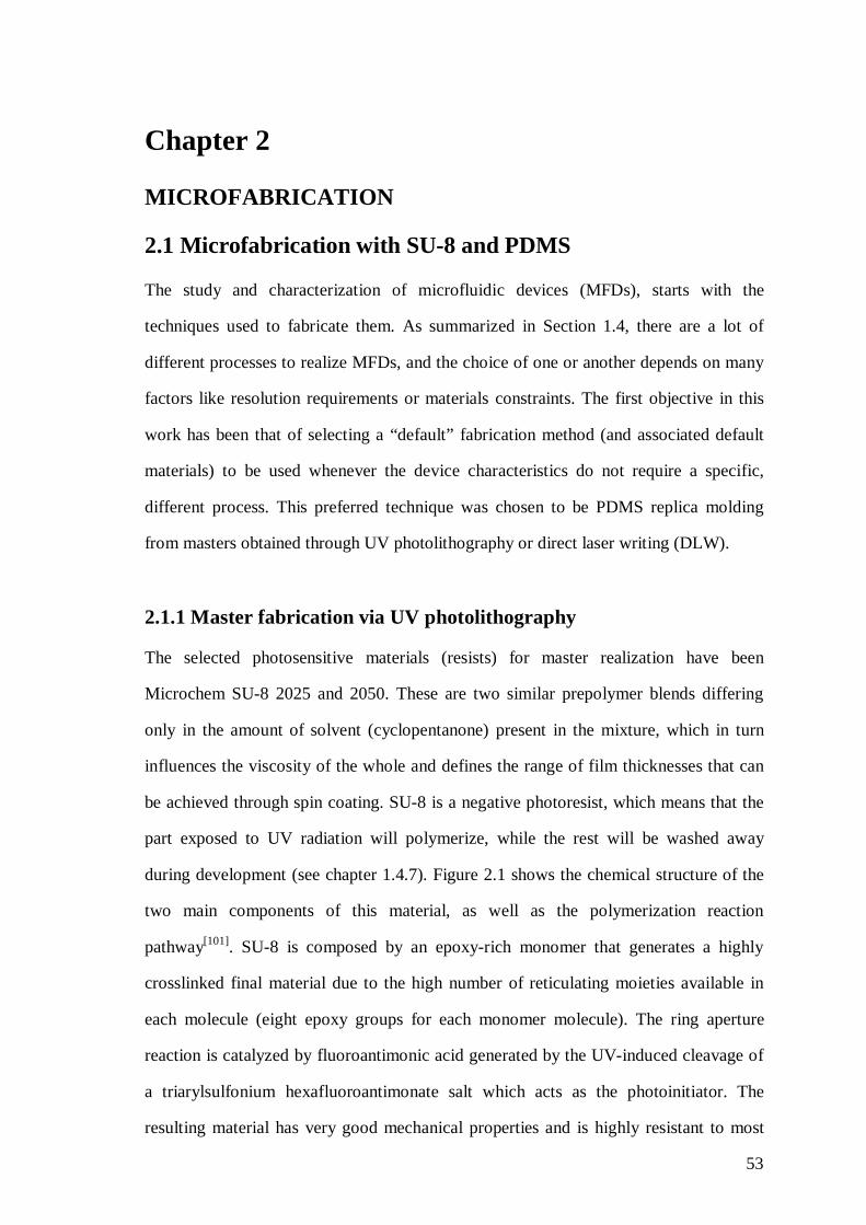
53
Chapter 2
MICROFABRICATION
2.1 Microfabrication with SU-8 and PDMS
The study and characterization of microfluidic devices (MFDs), starts with the
techniques used to fabricate them. As summarized in Section 1.4, there are a lot of
different processes to realize MFDs, and the choice of one or another depends on many
factors like resolution requirements or materials constraints. The first objective in this
work has been that of selecting a “default” fabrication method (and associated default
materials) to be used whenever the device characteristics do not require a specific,
different process. This preferred technique was chosen to be PDMS replica molding
from masters obtained through UV photolithography or direct laser writing (DLW).
2.1.1 Master fabrication via UV photolithography
The selected photosensitive materials (resists) for master realization have been
Microchem SU-8 2025 and 2050. These are two similar prepolymer blends differing
only in the amount of solvent (cyclopentanone) present in the mixture, which in turn
influences the viscosity of the whole and defines the range of film thicknesses that can
be achieved through spin coating. SU-8 is a negative photoresist, which means that the
part exposed to UV radiation will polymerize, while the rest will be washed away
during development (see chapter 1.4.7). Figure 2.1 shows the chemical structure of the
two main components of this material, as well as the polymerization reaction
pathway[101]. SU-8 is composed by an epoxy-rich monomer that generates a highly
crosslinked final material due to the high number of reticulating moieties available in
each molecule (eight epoxy groups for each monomer molecule). The ring aperture
reaction is catalyzed by fluoroantimonic acid generated by the UV-induced cleavage of
a triarylsulfonium hexafluoroantimonate salt which acts as the photoinitiator. The
resulting material has very good mechanical properties and is highly resistant to most
Microfabrication
54
solvents, allowing the realization
of resistant masters which if
needed can also feature
structures with high aspect ratio
(e.g. very high and thin
pillars)[101–103].
The standard sample preparation
is adapted from Microchem
guidelines*, and is summarized in
the following. A silicon substrate
is thoroughly cleaned with
deionized water and 2-propanol,
and is placed in a UV-ozone
(UVO) cleaner (Jelight model
42) for at least 10 minutes. This
step is required to activate the
sample surface by forcing the
creation of dangling bonds in the
native oxide surface that will
enhance the adhesion of the SU-8
microstructures to the substrate.
Without this extra step, there is a strong possibility that the photogenerated structures
will detach from the silicon during the following processes. Once the substrate is ready,
a thin film of SU-8 is deposited on the silicon via spin coating. The selected film
thickness depends on the desired thickness of the final structures. Using SU-8 2025 and
2050, thicknesses between 20 m and 70 m have been routinely obtained. If greater
thickness is required, two spin coater depositions (separated by a thermal treatment as
* Microchem guidelines are available at http://microchem.com/Prod-SU82000.htm.
Figure 2.1: a) chemical structure of one SU-8 monomer unit in unreacted (left) and polymerized (right) form. The high number of epoxy moieties in each monomer ensure extended crosslinking between different molecules; b) photoactivation reaction of SU-8 initiator; c) polymerization initiation by means of H+ catalyzed ring aperture; d) cationic polymerization propagation. (reproduced from [101])
Microfabrication
55
described below) can be performed on the same sample to increase the thickness up to
about 150 m. Regardless of film thickness, the sample is then subjected to a thermal
treatment to remove the excess solvent from the monomer. This is done in two steps,
increasing the temperature first to 65°C and then to 95°C to reduce thermal stress. The
exact duration of both steps depends on the film thickness (following Microchem
guidelines), but it must be kept well in mind that while a greatly overlong time can
compromise the following development, an incomplete solvent evaporation will surely
lead to a number of complications like decreased resolution, structure deformation or
detachment from the substrate. Once this treatment is complete, the sample is exposed
through an appropriated mask to the UV light to induce polymerization. The light
source used is a collimated UV lamp (Reinraumtechnik Lanz UV400) equipped with a
timer to ensure precise exposure time. Once again the exact time depends on the film
thickness. The masks are realized with a plotter by cutting holes in a black vinyl
adhesive and than attaching it to a microscope slide. Exposure is followed by another
thermal treatment with the same parameters of the first. This second bake is needed to
actually polymerize the material, since the initiator is generated during the exposure, but
the mobility of the involved chemical species at room temperature is too low to ensure
reticulation in timely fashion[104]. Finally, the sample is submerged in SU-8 Developer
(Microchem) under stirring until all the unexposed material is removed. The final
sample is rinsed with 2-propanol and is now ready to be replicated. Masters with
features down to 500 m have been realized with this technique. The cutting process
used to realized the masks leaves a slight roughness on the mask holes borders, which is
replicated on the structures during photolithography. However, this roughness never
exceeded 1-2 m.
2.1.2 Master fabrication via direct laser writing
While UV photolithography is a fast and efficient technique, some devices require
better resolution or greater flexibility. When this is the case, DLW has been employed
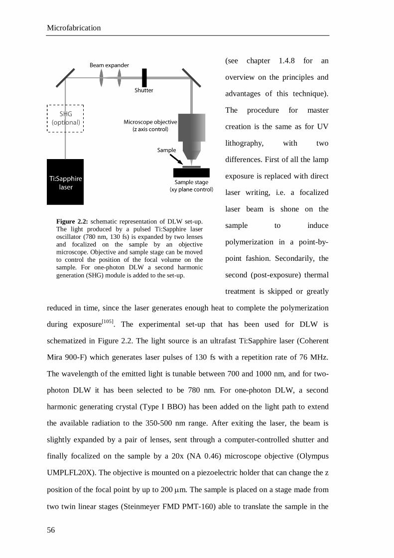
Microfabrication
56
(see chapter 1.4.8 for an
overview on the principles and
advantages of this technique).
The procedure for master
creation is the same as for UV
lithography, with two
differences. First of all the lamp
exposure is replaced with direct
laser writing, i.e. a focalized
laser beam is shone on the
sample to induce
polymerization in a point-by-
point fashion. Secondarily, the
second (post-exposure) thermal
treatment is skipped or greatly
reduced in time, since the laser generates enough heat to complete the polymerization
during exposure[105]. The experimental set-up that has been used for DLW is
schematized in Figure 2.2. The light source is an ultrafast Ti:Sapphire laser (Coherent
Mira 900-F) which generates laser pulses of 130 fs with a repetition rate of 76 MHz.
The wavelength of the emitted light is tunable between 700 and 1000 nm, and for two-
photon DLW it has been selected to be 780 nm. For one-photon DLW, a second
harmonic generating crystal (Type I BBO) has been added on the light path to extend
the available radiation to the 350-500 nm range. After exiting the laser, the beam is
slightly expanded by a pair of lenses, sent through a computer-controlled shutter and
finally focalized on the sample by a 20x (NA 0.46) microscope objective (Olympus
UMPLFL20X). The objective is mounted on a piezoelectric holder that can change the z
position of the focal point by up to 200 m. The sample is placed on a stage made from
two twin linear stages (Steinmeyer FMD PMT-160) able to translate the sample in the
Figure 2.2: schematic representation of DLW set-up. The light produced by a pulsed Ti:Sapphire laser oscillator (780 nm, 130 fs) is expanded by two lenses and focalized on the sample by an objective microscope. Objective and sample stage can be moved to control the position of the focal volume on the sample. For one-photon DLW a second harmonic generation (SHG) module is added to the set-up.
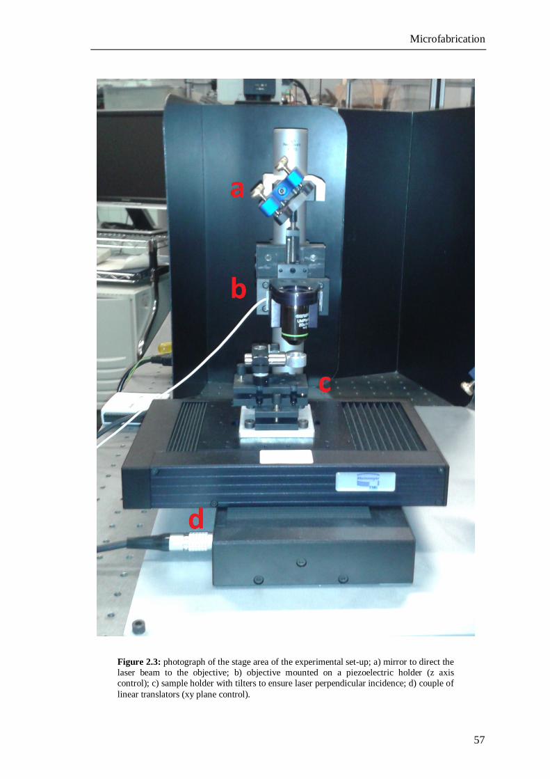
Microfabrication
57
Figure 2.3: photograph of the stage area of the experimental set-up; a) mirror to direct the laser beam to the objective; b) objective mounted on a piezoelectric holder (z axis control); c) sample holder with tilters to ensure laser perpendicular incidence; d) couple of linear translators (xy plane control).
Microfabrication
58
xy plane within a 100 cm2 square area with 0.5 m resolution. A photograph of the stage
area is shown in Figure 2.3. Sample stage, objective holder and shutter are all connected
to a computer. As part of this work, a labView program has been developed to integrate
control for all three elements, allowing the automated fabrication of structures ranging
from simple dots to complex figures delimited by segments or circular arcs. If two-
photon DLW is employed, three dimensional structures can be made in a plane-by-plane
fashion. This sort of automation is extremely useful since DLW is a serial process, and
as such can be quite time-consuming if the required structures cover a large area.
2.1.3 Replica molding
Once the master structure have been created, the final device is realized through the
replica molding technique[44] (see chapter 1.4.9). PDMS prepolymer and iniziator (Dow
Corning Sylgard 184) are mixed in a 10:1 ratio and then degassed in mild vacuum to
remove trapped air bubbles. The mixture is then poured over the master and subjected to
a thermal treatment in oven at 120° C for 1 hour. The sample is then brought back to
room temperature and the replica is peeled off from the master. Inlet and outlet holes
are punched through the PDMS. Finally, the replica and a flat slab of PDMS or glass
(e.g. a microscope slide or a coverglass) are treated with a UVO cleaner for 3 minutes to
create surface dangling bonds that can react with one another when the two surfaces are
brought into contact and kept at ~120°C for at least 1 hour. The result is a permanent
sealing that completes the device.
2.2 Beyond PDMS
It has been mentioned before (see Sections 1.4.2 and 1.4.9) that while PDMS and
replica molding are excellent ways to cheaply and rapidly produce MFDs, both suffer
from certain limitations. The one drawback that most strongly influences microfluidic
devices production is the limit imposed over microstructures shapes: replica molding
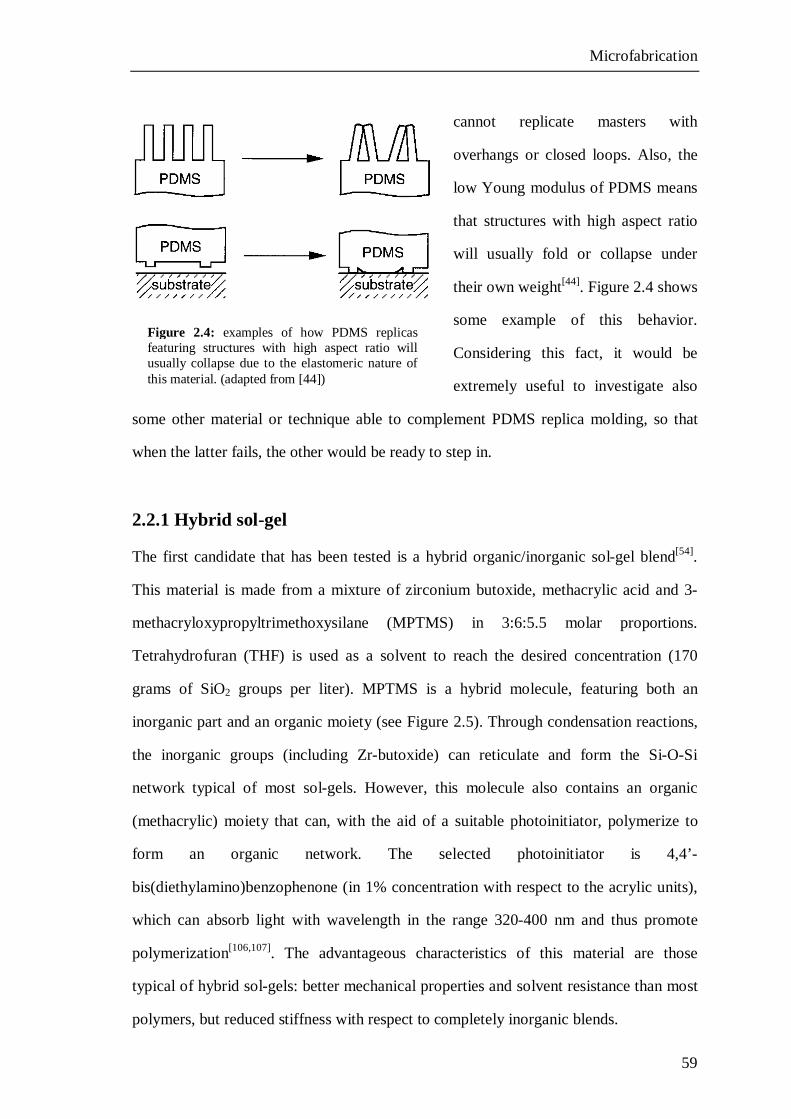
Microfabrication
59
cannot replicate masters with
overhangs or closed loops. Also, the
low Young modulus of PDMS means
that structures with high aspect ratio
will usually fold or collapse under
their own weight[44]. Figure 2.4 shows
some example of this behavior.
Considering this fact, it would be
extremely useful to investigate also
some other material or technique able to complement PDMS replica molding, so that
when the latter fails, the other would be ready to step in.
2.2.1 Hybrid sol-gel
The first candidate that has been tested is a hybrid organic/inorganic sol-gel blend[54].
This material is made from a mixture of zirconium butoxide, methacrylic acid and 3-
methacryloxypropyltrimethoxysilane (MPTMS) in 3:6:5.5 molar proportions.
Tetrahydrofuran (THF) is used as a solvent to reach the desired concentration (170
grams of SiO2 groups per liter). MPTMS is a hybrid molecule, featuring both an
inorganic part and an organic moiety (see Figure 2.5). Through condensation reactions,
the inorganic groups (including Zr-butoxide) can reticulate and form the Si-O-Si
network typical of most sol-gels. However, this molecule also contains an organic
(methacrylic) moiety that can, with the aid of a suitable photoinitiator, polymerize to
form an organic network. The selected photoinitiator is 4,4’-
bis(diethylamino)benzophenone (in 1% concentration with respect to the acrylic units),
which can absorb light with wavelength in the range 320-400 nm and thus promote
polymerization[106,107]. The advantageous characteristics of this material are those
typical of hybrid sol-gels: better mechanical properties and solvent resistance than most
polymers, but reduced stiffness with respect to completely inorganic blends.
Figure 2.4: examples of how PDMS replicas featuring structures with high aspect ratio will usually collapse due to the elastomeric nature of this material. (adapted from [44])
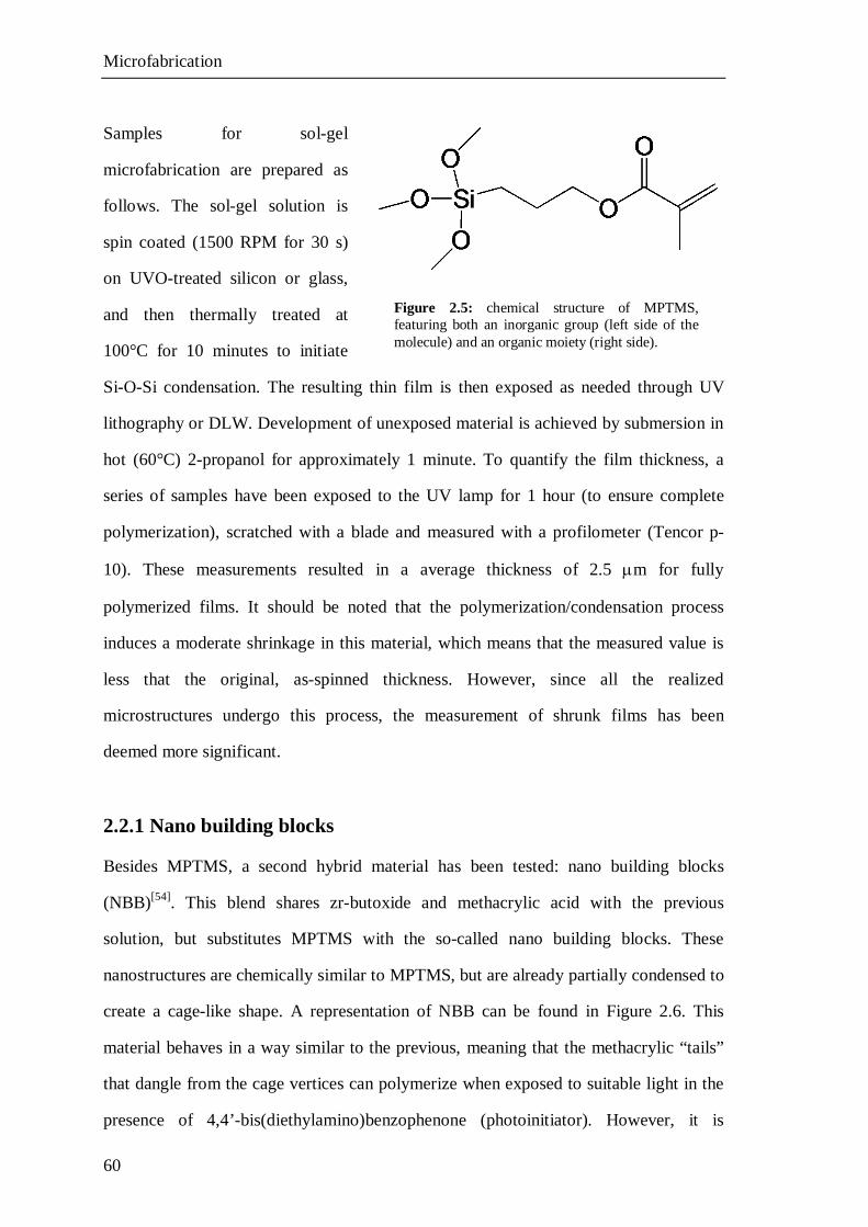
Microfabrication
60
Samples for sol-gel
microfabrication are prepared as
follows. The sol-gel solution is
spin coated (1500 RPM for 30 s)
on UVO-treated silicon or glass,
and then thermally treated at
100°C for 10 minutes to initiate
Si-O-Si condensation. The resulting thin film is then exposed as needed through UV
lithography or DLW. Development of unexposed material is achieved by submersion in
hot (60°C) 2-propanol for approximately 1 minute. To quantify the film thickness, a
series of samples have been exposed to the UV lamp for 1 hour (to ensure complete
polymerization), scratched with a blade and measured with a profilometer (Tencor p-
10). These measurements resulted in a average thickness of 2.5 m for fully
polymerized films. It should be noted that the polymerization/condensation process
induces a moderate shrinkage in this material, which means that the measured value is
less that the original, as-spinned thickness. However, since all the realized
microstructures undergo this process, the measurement of shrunk films has been
deemed more significant.
2.2.1 Nano building blocks
Besides MPTMS, a second hybrid material has been tested: nano building blocks
(NBB)[54]. This blend shares zr-butoxide and methacrylic acid with the previous
solution, but substitutes MPTMS with the so-called nano building blocks. These
nanostructures are chemically similar to MPTMS, but are already partially condensed to
create a cage-like shape. A representation of NBB can be found in Figure 2.6. This
material behaves in a way similar to the previous, meaning that the methacrylic “tails”
that dangle from the cage vertices can polymerize when exposed to suitable light in the
presence of 4,4’-bis(diethylamino)benzophenone (photoinitiator). However, it is
Figure 2.5: chemical structure of MPTMS, featuring both an inorganic group (left side of the molecule) and an organic moiety (right side).
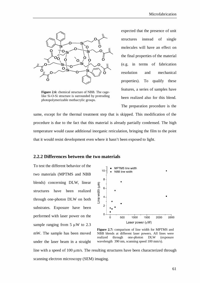
Microfabrication
61
expected that the presence of unit
structures instead of single
molecules will have an effect on
the final properties of the material
(e.g. in terms of fabrication
resolution and mechanical
properties). To qualify these
features, a series of samples have
been realized also for this blend.
The preparation procedure is the
same, except for the thermal treatment step that is skipped. This modification of the
procedure is due to the fact that this material is already partially condensed. The high
temperature would cause additional inorganic reticulation, bringing the film to the point
that it would resist development even where it hasn’t been exposed to light.
2.2.2 Differences between the two materials
To test the different behavior of the
two materials (MPTMS and NBB
blends) concerning DLW, linear
structures have been realized
through one-photon DLW on both
substrates. Exposure have been
performed with laser power on the
sample ranging from 5 W to 2.3
mW. The sample has been moved
under the laser beam in a straight
line with a speed of 100 m/s. The resulting structures have been characterized through
scanning electron microscopy (SEM) imaging.
Figure 2.6: chemical structure of NBB. The cage-like Si-O-Si structure is surrounded by protruding photopolymerizable methacrylic groups.
Figure 2.7: comparison of line width for MPTMS and NBB blends at different laser powers. All lines were realized through one-photon DLW (exposure wavelength 390 nm, scanning speed 100 mm/s).
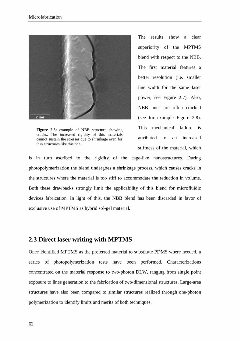
Microfabrication
62
The results show a clear
superiority of the MPTMS
blend with respect to the NBB.
The first material features a
better resolution (i.e. smaller
line width for the same laser
power, see Figure 2.7). Also,
NBB lines are often cracked
(see for example Figure 2.8).
This mechanical failure is
attributed to an increased
stiffness of the material, which
is in turn ascribed to the rigidity of the cage-like nanostructures. During
photopolymerization the blend undergoes a shrinkage process, which causes cracks in
the structures where the material is too stiff to accommodate the reduction in volume.
Both these drawbacks strongly limit the applicability of this blend for microfluidic
devices fabrication. In light of this, the NBB blend has been discarded in favor of
exclusive use of MPTMS as hybrid sol-gel material.
2.3 Direct laser writing with MPTMS
Once identified MPTMS as the preferred material to substitute PDMS where needed, a
series of photopolymerization tests have been performed. Characterizations
concentrated on the material response to two-photon DLW, ranging from single point
exposure to lines generation to the fabrication of two-dimensional structures. Large-area
structures have also been compared to similar structures realized through one-photon
polymerization to identify limits and merits of both techniques.
Figure 2.8: example of NBB structure showing cracks. The increased rigidity of this materials cannot sustain the stresses due to shrinkage even for thin structures like this one.
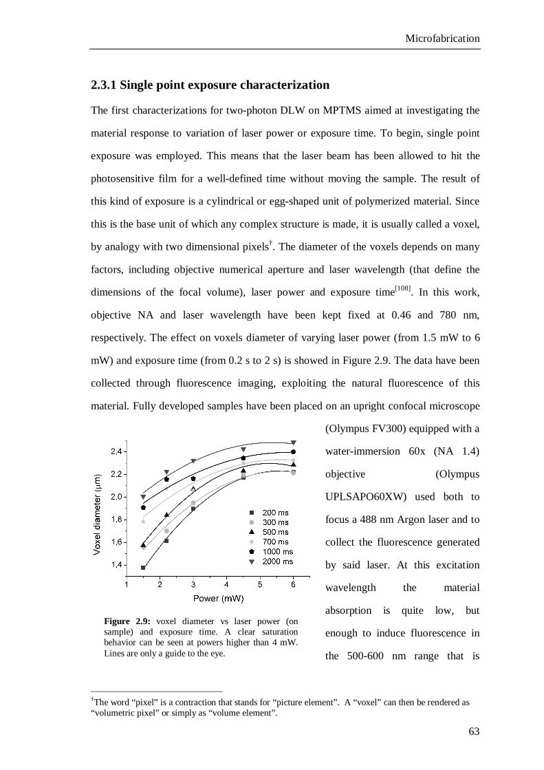
Microfabrication
63
2.3.1 Single point exposure characterization
The first characterizations for two-photon DLW on MPTMS aimed at investigating the
material response to variation of laser power or exposure time. To begin, single point
exposure was employed. This means that the laser beam has been allowed to hit the
photosensitive film for a well-defined time without moving the sample. The result of
this kind of exposure is a cylindrical or egg-shaped unit of polymerized material. Since
this is the base unit of which any complex structure is made, it is usually called a voxel,
by analogy with two dimensional pixels†. The diameter of the voxels depends on many
factors, including objective numerical aperture and laser wavelength (that define the
dimensions of the focal volume), laser power and exposure time[108]. In this work,
objective NA and laser wavelength have been kept fixed at 0.46 and 780 nm,
respectively. The effect on voxels diameter of varying laser power (from 1.5 mW to 6
mW) and exposure time (from 0.2 s to 2 s) is showed in Figure 2.9. The data have been
collected through fluorescence imaging, exploiting the natural fluorescence of this
material. Fully developed samples have been placed on an upright confocal microscope
(Olympus FV300) equipped with a
water-immersion 60x (NA 1.4)
objective (Olympus
UPLSAPO60XW) used both to
focus a 488 nm Argon laser and to
collect the fluorescence generated
by said laser. At this excitation
wavelength the material
absorption is quite low, but
enough to induce fluorescence in
the 500-600 nm range that is
†The word “pixel” is a contraction that stands for “picture element”. A “voxel” can then be rendered as “volumetric pixel” or simply as “volume element”.
Figure 2.9: voxel diameter vs laser power (on sample) and exposure time. A clear saturation behavior can be seen at powers higher than 4 mW. Lines are only a guide to the eye.
Microfabrication
64
recorded by the detector (photomultiplier tube). The confocal geometry (100 m
pinhole) ensure that out-of-focus fluorescence is not revealed. The error on voxel
dimension measurements is estimated to be 0.3 m.
Observing Figure 2.9 progressive increase of voxel diameters with increasing laser
power and/or exposure time can be easily seen. This behavior is expected, since only
the beam area that exceeds a specific threshold intensity can promote
photopolymerization. The radius w0 of the focal area on the sample can be deduced
from Gaussian optics laws[109]:
02wNA
(2.1)
where is the laser wavelength and NA is the numerical aperture of the focalizing
objective. Considering NA = 0.46 and = 780 nm, a focal radius of 1.08 m is obtained.
Considering that the spatial intensity distribution of the laser beam on the sample
follows a Gaussian profile, it can be predicted that a reduction in overall laser power
will cause a smaller polymerized area (see Section 1.4.8). A similar reasoning can be
made for exposure time, taking into account the fact that even below-threshold intensity
can interact with the photoinitiator and, in due time, generate enough reactive species to
trigger polymerization. The trend of voxel diameter d with laser power and exposure
time can be expressed as[108]:
12 20
0 ln eff N f td w
C
(2.2)
where f is the repetition rate of the pulsed laser, is the pulse duration, t the exposition
time and eff is the product of the initiator two-photon absorption cross section 2 and
the efficiency of the initiation process ( < 1). N0 is the photon flux, which can be
expressed as:
0 20
PNf h w
(2.3)
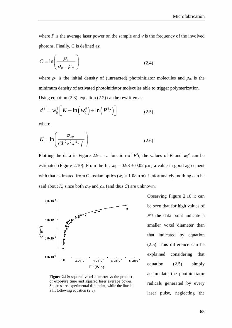
Microfabrication
65
where P is the average laser power on the sample and is the frequency of the involved
photons. Finally, C is defined as:
0
0
lnth
C
(2.4)
where 0 is the initial density of (unreacted) photoinitiator molecules and th is the
minimum density of activated photoinitiator molecules able to trigger polymerization.
Using equation (2.3), equation (2.2) can be rewritten as:
2 2 4 20 0ln lnd w K w P t (2.5)
where
2 2 2ln effKCh f
(2.6)
Plotting the data in Figure 2.9 as a function of P2t, the values of K and w02 can be
estimated (Figure 2.10). From the fit, w0 = 0.93 0.02 m, a value in good agreement
with that estimated from Gaussian optics (w0 = 1.08 m). Unfortunately, nothing can be
said about K, since both eff and th (and thus C) are unknown.
Observing Figure 2.10 it can
be seen that for high values of
P2t the data point indicate a
smaller voxel diameter than
that indicated by equation
(2.5). This difference can be
explained considering that
equation (2.5) simply
accumulate the photoinitiator
radicals generated by every
laser pulse, neglecting the
Figure 2.10: squared voxel diameter vs the product of exposure time and squared laser average power. Squares are experimental data point, while the line is a fit following equation (2.5).
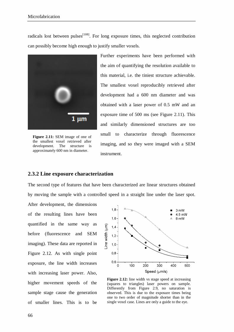
Microfabrication
66
radicals lost between pulses[108]. For long exposure times, this neglected contribution
can possibly become high enough to justify smaller voxels.
Further experiments have been performed with
the aim of quantifying the resolution available to
this material, i.e. the tiniest structure achievable.
The smallest voxel reproducibly retrieved after
development had a 600 nm diameter and was
obtained with a laser power of 0.5 mW and an
exposure time of 500 ms (see Figure 2.11). This
and similarly dimensioned structures are too
small to characterize through fluorescence
imaging, and so they were imaged with a SEM
instrument.
2.3.2 Line exposure characterization
The second type of features that have been characterized are linear structures obtained
by moving the sample with a controlled speed in a straight line under the laser spot.
After development, the dimensions
of the resulting lines have been
quantified in the same way as
before (fluorescence and SEM
imaging). These data are reported in
Figure 2.12. As with single point
exposure, the line width increases
with increasing laser power. Also,
higher movement speeds of the
sample stage cause the generation
of smaller lines. This is to be
Figure 2.11: SEM image of one of the smallest voxel retrieved after development. The structure is approximately 600 nm in diameter.
Figure 2.12: line width vs stage speed at increasing (squares to triangles) laser powers on sample. Differently from Figure 2.9, no saturation is observed. This is due to the exposure times being one to two order of magnitude shorter than in the single voxel case. Lines are only a guide to the eye.
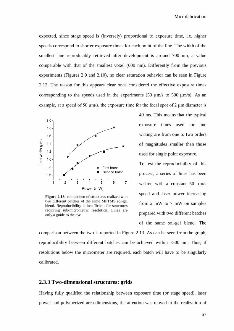
Microfabrication
67
expected, since stage speed is (inversely) proportional to exposure time, i.e. higher
speeds correspond to shorter exposure times for each point of the line. The width of the
smallest line reproducibly retrieved after development is around 700 nm, a value
comparable with that of the smallest voxel (600 nm). Differently from the previous
experiments (Figures 2.9 and 2.10), no clear saturation behavior can be seen in Figure
2.12. The reason for this appears clear once considered the effective exposure times
corresponding to the speeds used in the experiments (50 m/s to 500 m/s). As an
example, at a speed of 50 µm/s, the exposure time for the focal spot of 2 μm diameter is
40 ms. This means that the typical
exposure times used for line
writing are from one to two orders
of magnitudes smaller than those
used for single point exposure.
To test the reproducibility of this
process, a series of lines has been
written with a constant 50 m/s
speed and laser power increasing
from 2 mW to 7 mW on samples
prepared with two different batches
of the same sol-gel blend. The
comparison between the two is reported in Figure 2.13. As can be seen from the graph,
reproducibility between different batches can be achieved within ~500 nm. Thus, if
resolutions below the micrometer are required, each batch will have to be singularly
calibrated.
2.3.3 Two-dimensional structures: grids
Having fully qualified the relationship between exposure time (or stage speed), laser
power and polymerized area dimensions, the attention was moved to the realization of
Figure 2.13: comparison of structures realized with two different batches of the same MPTMS sol-gel blend. Reproducibility is insufficient for structures requiring sub-micrometric resolution. Lines are only a guide to the eye.
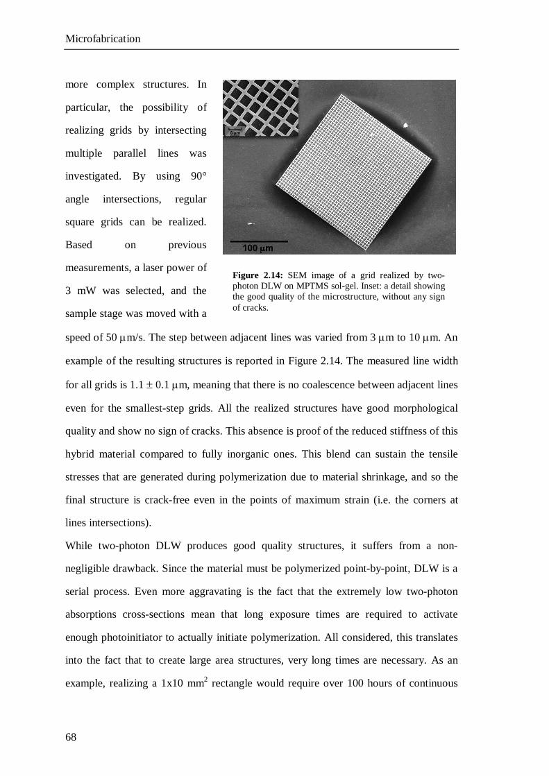
Microfabrication
68
more complex structures. In
particular, the possibility of
realizing grids by intersecting
multiple parallel lines was
investigated. By using 90°
angle intersections, regular
square grids can be realized.
Based on previous
measurements, a laser power of
3 mW was selected, and the
sample stage was moved with a
speed of 50 m/s. The step between adjacent lines was varied from 3 m to 10 m. An
example of the resulting structures is reported in Figure 2.14. The measured line width
for all grids is 1.1 0.1 m, meaning that there is no coalescence between adjacent lines
even for the smallest-step grids. All the realized structures have good morphological
quality and show no sign of cracks. This absence is proof of the reduced stiffness of this
hybrid material compared to fully inorganic ones. This blend can sustain the tensile
stresses that are generated during polymerization due to material shrinkage, and so the
final structure is crack-free even in the points of maximum strain (i.e. the corners at
lines intersections).
While two-photon DLW produces good quality structures, it suffers from a non-
negligible drawback. Since the material must be polymerized point-by-point, DLW is a
serial process. Even more aggravating is the fact that the extremely low two-photon
absorptions cross-sections mean that long exposure times are required to activate
enough photoinitiator to actually initiate polymerization. All considered, this translates
into the fact that to create large area structures, very long times are necessary. As an
example, realizing a 1x10 mm2 rectangle would require over 100 hours of continuous
Figure 2.14: SEM image of a grid realized by two-photon DLW on MPTMS sol-gel. Inset: a detail showing the good quality of the microstructure, without any sign of cracks.
Microfabrication
69
laser operation. Thus, the possibility of generating grids through one-photon DLW was
explored.
2.3.4 One-photon microfabrication
The absorption (and corresponding polymerization) efficiency of one- and two-photon
processes can be markedly different. As already mentioned in Section 1.4.8, intensity
reduction due to absorption can be quantified as:
2dI I Idz
(1.3)
where I is the light intensity and and are respectively the first- and second-order
absorption coefficients. Separating the two contributes leads to:
first order
dI Idz
(2.7)
2
second order
dI I I Idz
(2.8)
While linear absorption efficiency is constant for all intensities, nonlinear efficiency
increases at high light intensities. Thus, for any comparison it is necessary to choose a
specific intensity value. In the work here reported, the average laser power P on sample
for two-photon DLW is on the order of 1 mW. Since the laser output is pulsed with a
frequency of 76 MHz and a pulse duration of 120 fs, the peak power Ppeak during
exposure is:
100 WpeakPP
(2.9)
The radius w0 of the focal area can be estimated from:
02wNA
(2.1)
Microfabrication
70
where is the laser wavelength and NA is the numerical aperture of the focalizing
objective. Considering NA = 0.46 and = 780 nm, a focal radius of ~1 m is obtained,
leading to an intensity I on the order of:
282 2 20
GW photons3 10 cm cm s
peakPI
w (2.10)
Typical values[110] of for UV lithography photoinitiators (such as the one used in this
work) are on the order of 10 GM‡, while values for average around 10-15 cm2. This
means that for the intensities reported above the ratio between the efficiencies is on the
order of:
510I
(2.11)
As can be seen, one-photon absorption in much more efficient than the second-order
process. During DLW this increased efficiency translates into shorter exposure times
needed to induce polymerization, which in turn allows faster fabrication of large-area
structures. Unfortunately this gain in time corresponds to a decrease in terms of
resolution. One-photon processes are less intensity-dependant than non-linear ones, and
so it is very difficult (if not outright impossible) to realize structures with dimensions
under a few micrometers by simply reducing the laser power or the exposure time.
Attempts to do so will usually result in no polymerization whatsoever. Despite this
limitation, one-photon DLW would be quite useful for large area, low resolution tasks.
For this reason, 10 m and 20 m step grids have been realized with frequency doubled
laser light (wavelength 390 nm), 500 W laser power on sample and 2000 m/s and
1400 m/s stage speeds, respectively. A microscope image showing the typical results
is reported in Figure 2.15. Marked overpolymerization at line intersection can be seen in
the image, and most of the corners show cracks. Attempts to lower the laser power, or
‡ The Goeppert-Mayer is a unit for the two-photon absorption cross section.
4-50 cm s1 GM = 10
photon
Microfabrication
71
increase the stage speed resulted in no polymerization at all. This poor result is the
product of two different factors. The strong absorption of the photoinitiator due to one-
photon processes translates into a high local concentration of activated initiator, which
in turn leads to fast polymerization (accentuating the risk of cracks) and to diffusion
outside the target area (which degrades resolution). Moreover, the reduced stiffness of
this hybrid material allows
some accommodation of tensile
stress due to shrinkage, but
evidently not enough to realize
crack-free structures with more
than one dimension exceeding
1-2 m (i.e. 1 m thin lines can
be hundreds of micrometers
long, but 10 m wide lines will
usually crack). This means that
this hybrid sol-gel material is
unsuitable for bulk MFD
fabrication. However, its other
qualities make it an excellent candidate for channel internal sub-structuration. As an
example, the desired features could be realized on a coverglass which is then used to
seal a network of channels engraved on PDMS. A possible limit to this approach is the
fact that this procedure requires a mask aligner or similar instrument to ensure that
channel and sub-structuration are not misaligned.
2.3.5 Biocompatibility
To further extend the potential usefulness of this material, the biocompatibility of the
fully polymerized form was tested. This characterization is very important in light of the
recent interest of the scientific community towards MFDs for biological applications
Figure 2.15: optical microscope image of a grid (step 20 m) realized through one-photon DLW (power 0.5 mW; scanning speed 1400 m/s). Cracks can be seen at corners, and line intersections are overpolymerized.
Microfabrication
72
(see Section 1.1.4). The biocompatibility tests were performed by realizing a series of
glass samples covered with a flat layer of the MPTMS blend. The sol-gel was kept
under the UV lamp for 30 minutes, turned upside down and exposed for another 30
minutes to ensure complete polymerization of the film. After the thermal treatment, the
samples were submerged in the development solution (hot 2-propanol) to remove any
surviving non-polymerized part that could be present. Following this, the substrates
were inserted at the bottom of the wells of a standard 24 multiwell plate (SGW) and
then exposed again to UV light for two hours in order to sterilize the material. After
sterilization the sol-gel surface
was functionalized with a 0.5
μg/μL fibronectin solution. This
molecule is a promoter for
cellular adhesion, and is
commonly used in most
biologically oriented
MFDs[111,112]. Finally, human
umbilical vein endothelial cells
(HUVEC) were seeded on the
samples, and cultured in
endothelial cell basal medium
(EBM) supplemented with 10% fetal bovine serum (FBS), 100 IU/ml penicillin and 100
mg/l streptomycin. A microscope image of these cells attached on the sol-gel substrate
is shown in Figure 2.16. HUVEC cells were chosen because they are primary cells and
as such can be considered a good benchmark for biocompatibility of artificial materials.
Indeed their proliferation and viability is more sensitive to the chemical and physical
characteristic of the material on which they grow, with respect to cancer line cells or
similar more sturdy cell cultures. HUVEC proliferation was tested using a colorimetric
assay (Biosource International) based on the redox sensor alamarBlue. The alamarBlue
Figure 2.16: optical microscope image of HUVEC cells grown on a completely polymerized MPTMS sol-gel substrate.
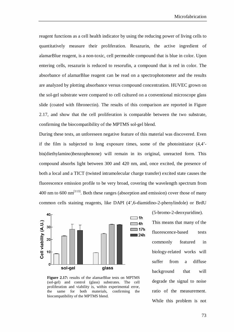
Microfabrication
73
reagent functions as a cell health indicator by using the reducing power of living cells to
quantitatively measure their proliferation. Resazurin, the active ingredient of
alamarBlue reagent, is a non-toxic, cell permeable compound that is blue in color. Upon
entering cells, resazurin is reduced to resorufin, a compound that is red in color. The
absorbance of alamarBlue reagent can be read on a spectrophotometer and the results
are analyzed by plotting absorbance versus compound concentration. HUVEC grown on
the sol-gel substrate were compared to cell cultured on a conventional microscope glass
slide (coated with fibronectin). The results of this comparison are reported in Figure
2.17, and show that the cell proliferation is comparable between the two substrate,
confirming the biocompatibility of the MPTMS sol-gel blend.
During these tests, an unforeseen negative feature of this material was discovered. Even
if the film is subjected to long exposure times, some of the photoinitiator (4,4’-
bis(diethylamino)benzophenone) will remain in its original, unreacted form. This
compound absorbs light between 300 and 420 nm, and, once excited, the presence of
both a local and a TICT (twisted intramolecular charge transfer) excited state causes the
fluorescence emission profile to be very broad, covering the wavelength spectrum from
400 nm to 600 nm[113]. Both these ranges (absorption and emission) cover those of many
common cells staining reagents, like DAPI (4’,6-diamidino-2-phenylindole) or BrdU
(5-bromo-2-deoxyuridine).
This means that many of the
fluorescence-based tests
commonly featured in
biology-related works will
suffer from a diffuse
background that will
degrade the signal to noise
ratio of the measurement.
While this problem is not
Figure 2.17: results of the alamarBlue tests on MPTMS (sol-gel) and control (glass) substrates. The cell proliferation and viability is, within experimental error, the same for both materials, confirming the biocompatibility of the MPTMS blend.
Microfabrication
74
unsolvable (e.g. different fluorescent labels can be used), it poses certain limitations to
biological applications in MFDs realized with this material.
2.3.6 Final remarks on MPTMS
Summarizing what has been assessed in this chapter, the MPTMS hybrid
organic/inorganic sol-gel blend poses itself as a good candidate for the fabrication of
microstructures that for any reason (e.g. shape or solvent incompatibility) cannot be
made in PDMS or by replica molding. While attempting to realize big, large structures
will usually result in cracked surfaces, small feature can be realized with excellent
resolution (~600 nm) through two-photon direct laser writing. Being biocompatible, this
material is also available for MFDs dedicated to biological applications. However, the
native fluorescence of residual unreacted photoinitiator can cause a diffuse background
in many fluorescence-based tests, degrading the measurement signal to noise ratio.
Notwithstanding these limitations, this sol-gel blend can be very useful especially for
the internal sub-structuration of microchannels.
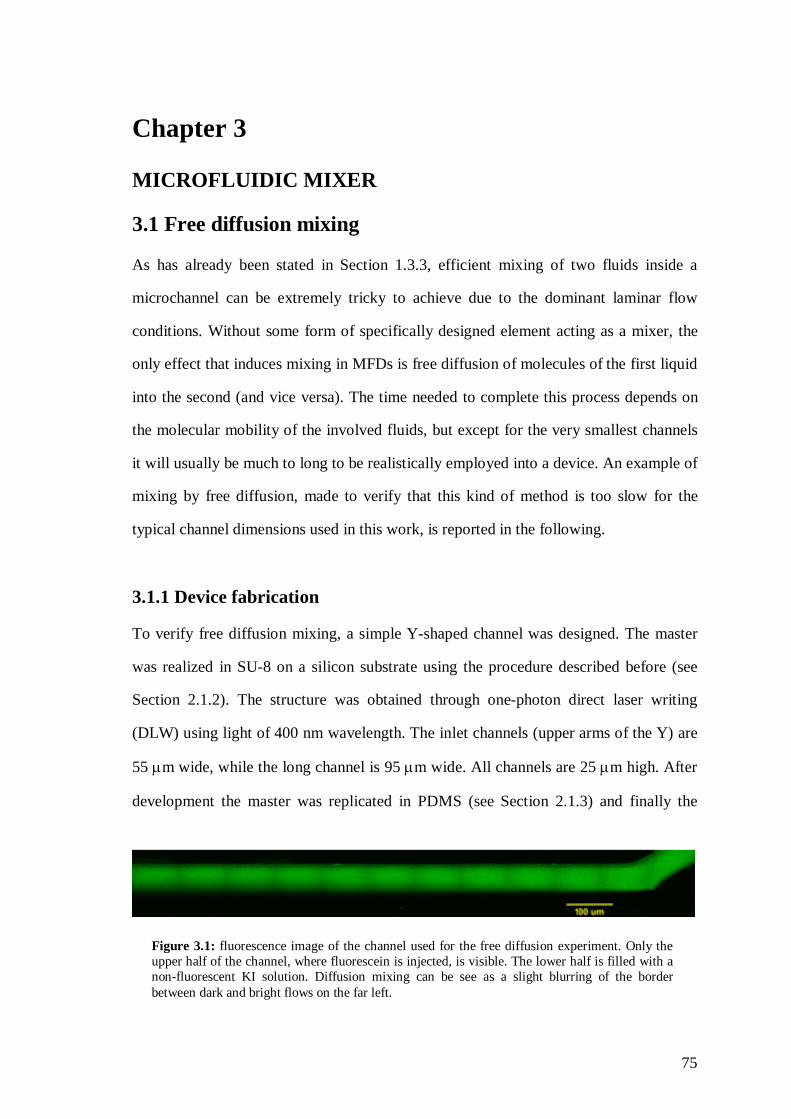
75
Chapter 3
MICROFLUIDIC MIXER
3.1 Free diffusion mixing
As has already been stated in Section 1.3.3, efficient mixing of two fluids inside a
microchannel can be extremely tricky to achieve due to the dominant laminar flow
conditions. Without some form of specifically designed element acting as a mixer, the
only effect that induces mixing in MFDs is free diffusion of molecules of the first liquid
into the second (and vice versa). The time needed to complete this process depends on
the molecular mobility of the involved fluids, but except for the very smallest channels
it will usually be much to long to be realistically employed into a device. An example of
mixing by free diffusion, made to verify that this kind of method is too slow for the
typical channel dimensions used in this work, is reported in the following.
3.1.1 Device fabrication
To verify free diffusion mixing, a simple Y-shaped channel was designed. The master
was realized in SU-8 on a silicon substrate using the procedure described before (see
Section 2.1.2). The structure was obtained through one-photon direct laser writing
(DLW) using light of 400 nm wavelength. The inlet channels (upper arms of the Y) are
55 m wide, while the long channel is 95 m wide. All channels are 25 m high. After
development the master was replicated in PDMS (see Section 2.1.3) and finally the
Figure 3.1: fluorescence image of the channel used for the free diffusion experiment. Only the upper half of the channel, where fluorescein is injected, is visible. The lower half is filled with a non-fluorescent KI solution. Diffusion mixing can be see as a slight blurring of the border between dark and bright flows on the far left.
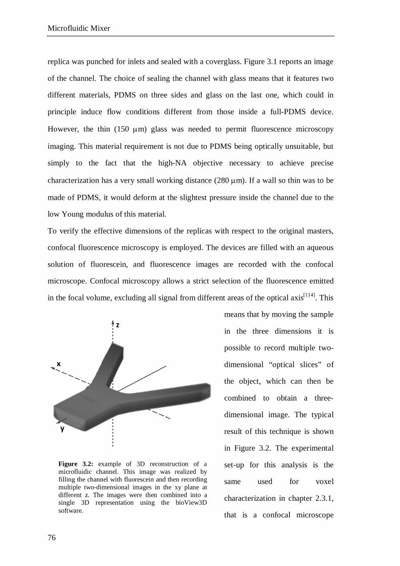
Microfluidic Mixer
76
replica was punched for inlets and sealed with a coverglass. Figure 3.1 reports an image
of the channel. The choice of sealing the channel with glass means that it features two
different materials, PDMS on three sides and glass on the last one, which could in
principle induce flow conditions different from those inside a full-PDMS device.
However, the thin (150 m) glass was needed to permit fluorescence microscopy
imaging. This material requirement is not due to PDMS being optically unsuitable, but
simply to the fact that the high-NA objective necessary to achieve precise
characterization has a very small working distance (280 m). If a wall so thin was to be
made of PDMS, it would deform at the slightest pressure inside the channel due to the
low Young modulus of this material.
To verify the effective dimensions of the replicas with respect to the original masters,
confocal fluorescence microscopy is employed. The devices are filled with an aqueous
solution of fluorescein, and fluorescence images are recorded with the confocal
microscope. Confocal microscopy allows a strict selection of the fluorescence emitted
in the focal volume, excluding all signal from different areas of the optical axis[114]. This
means that by moving the sample
in the three dimensions it is
possible to record multiple two-
dimensional “optical slices” of
the object, which can then be
combined to obtain a three-
dimensional image. The typical
result of this technique is shown
in Figure 3.2. The experimental
set-up for this analysis is the
same used for voxel
characterization in chapter 2.3.1,
that is a confocal microscope
Figure 3.2: example of 3D reconstruction of a microfluidic channel. This image was realized by filling the channel with fluorescein and then recording multiple two-dimensional images in the xy plane at different z. The images were then combined into a single 3D representation using the bioView3D software.
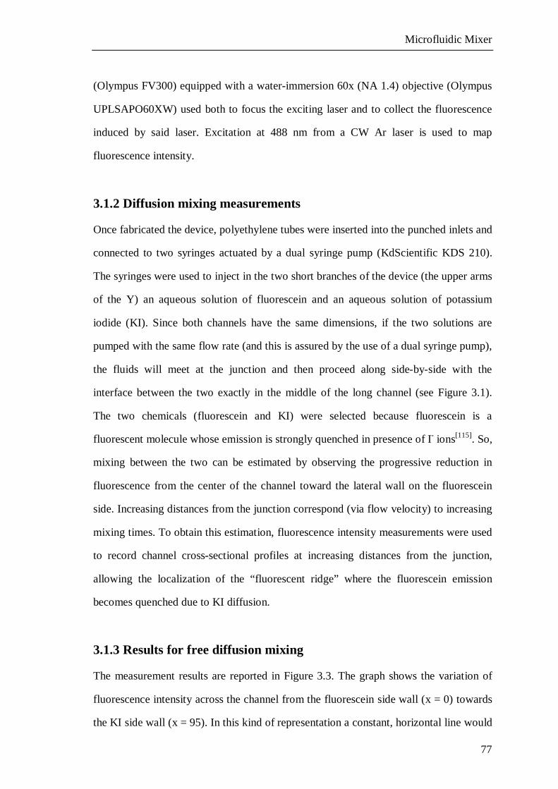
Microfluidic Mixer
77
(Olympus FV300) equipped with a water-immersion 60x (NA 1.4) objective (Olympus
UPLSAPO60XW) used both to focus the exciting laser and to collect the fluorescence
induced by said laser. Excitation at 488 nm from a CW Ar laser is used to map
fluorescence intensity.
3.1.2 Diffusion mixing measurements
Once fabricated the device, polyethylene tubes were inserted into the punched inlets and
connected to two syringes actuated by a dual syringe pump (KdScientific KDS 210).
The syringes were used to inject in the two short branches of the device (the upper arms
of the Y) an aqueous solution of fluorescein and an aqueous solution of potassium
iodide (KI). Since both channels have the same dimensions, if the two solutions are
pumped with the same flow rate (and this is assured by the use of a dual syringe pump),
the fluids will meet at the junction and then proceed along side-by-side with the
interface between the two exactly in the middle of the long channel (see Figure 3.1).
The two chemicals (fluorescein and KI) were selected because fluorescein is a
fluorescent molecule whose emission is strongly quenched in presence of I- ions[115]. So,
mixing between the two can be estimated by observing the progressive reduction in
fluorescence from the center of the channel toward the lateral wall on the fluorescein
side. Increasing distances from the junction correspond (via flow velocity) to increasing
mixing times. To obtain this estimation, fluorescence intensity measurements were used
to record channel cross-sectional profiles at increasing distances from the junction,
allowing the localization of the “fluorescent ridge” where the fluorescein emission
becomes quenched due to KI diffusion.
3.1.3 Results for free diffusion mixing
The measurement results are reported in Figure 3.3. The graph shows the variation of
fluorescence intensity across the channel from the fluorescein side wall (x = 0) towards
the KI side wall (x = 95). In this kind of representation a constant, horizontal line would
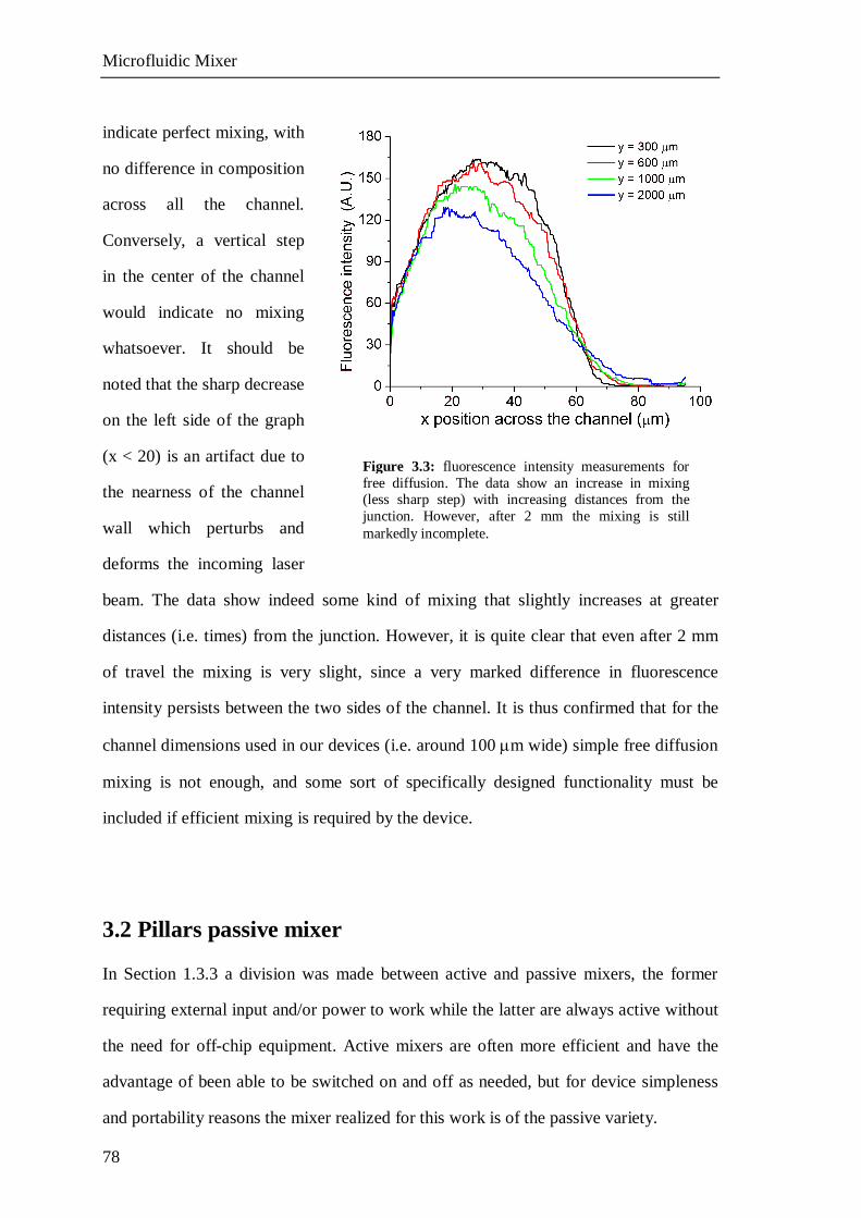
Microfluidic Mixer
78
indicate perfect mixing, with
no difference in composition
across all the channel.
Conversely, a vertical step
in the center of the channel
would indicate no mixing
whatsoever. It should be
noted that the sharp decrease
on the left side of the graph
(x < 20) is an artifact due to
the nearness of the channel
wall which perturbs and
deforms the incoming laser
beam. The data show indeed some kind of mixing that slightly increases at greater
distances (i.e. times) from the junction. However, it is quite clear that even after 2 mm
of travel the mixing is very slight, since a very marked difference in fluorescence
intensity persists between the two sides of the channel. It is thus confirmed that for the
channel dimensions used in our devices (i.e. around 100 m wide) simple free diffusion
mixing is not enough, and some sort of specifically designed functionality must be
included if efficient mixing is required by the device.
3.2 Pillars passive mixer
In Section 1.3.3 a division was made between active and passive mixers, the former
requiring external input and/or power to work while the latter are always active without
the need for off-chip equipment. Active mixers are often more efficient and have the
advantage of been able to be switched on and off as needed, but for device simpleness
and portability reasons the mixer realized for this work is of the passive variety.
Figure 3.3: fluorescence intensity measurements for free diffusion. The data show an increase in mixing (less sharp step) with increasing distances from the junction. However, after 2 mm the mixing is still markedly incomplete.
Microfluidic Mixer
79
3.2.2 Mixer design
To be able to mix different fluids inside a MFD, a mixer module must be able to
overcome the dominating laminar conditions. One way to do that is to locally perturb
the system to relax laminar constrains. Vectorially speaking, laminar motion means that
the velocity of any infinitesimally small volume of fluid has only one component,
parallel to the channel axis (which is usually dubbed the y axis), and this fact is the
reason why mixing in laminar conditions is so difficult. Regardless of this, if there is an
obstacle inside the channel, so that the fluid physically cannot maintain its straight-on
direction, the flow will necessarily bend around the obstacle. This bending means that
laminar conditions are locally relaxed and mixing can be achieved.
Unfortunately, building an obstacle inside a microchannel will formally perturb laminar
condition, but most often the perturbation will be limited in both magnitude and spatial
extension, meaning that very little mixing will be achieved before the fluid restores
itself to its preferred laminar motion. However, such perturbation can be extended and
magnified if multiple, carefully placed obstacles are used instead of a single one. With
this consideration in mind, the attention was posed to the design of a microfluidic
mixing module based on a channel featuring multiple internal obstacles. To help tune
design parameters such as number, size and position of obstacles, a preliminary
screening of tentative device designs was performed through numerical simulations
with the aid of the commercial COMSOL 3.5 software. The simulated devices feature a
T junction where two fluids are injected with a flow speed of 1 mm/s from the two short
arms and meet at the junction. Both then flow along a straight channel containing
various obstacles. The first fluid is pure solvent, while the second is a solution of a
given chemical species. Considering the laminar conditions inside the channel, the
Navier-Stokes and convective-diffusive equations for the species to be mixed can be
expressed as[116]:
2ˆ 0ij i
j i
u pu ur r
(3.1)
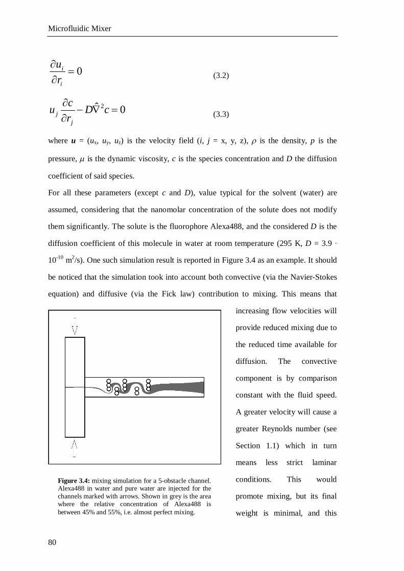
Microfluidic Mixer
80
0i
i
ur
(3.2)
2ˆ 0jj
cu D cr
(3.3)
where u = (ux, uy, uz) is the velocity field (i, j = x, y, z), is the density, p is the
pressure, is the dynamic viscosity, c is the species concentration and D the diffusion
coefficient of said species.
For all these parameters (except c and D), value typical for the solvent (water) are
assumed, considering that the nanomolar concentration of the solute does not modify
them significantly. The solute is the fluorophore Alexa488, and the considered D is the
diffusion coefficient of this molecule in water at room temperature (295 K, D = 3.9 ∙
10-10 m2/s). One such simulation result is reported in Figure 3.4 as an example. It should
be noticed that the simulation took into account both convective (via the Navier-Stokes
equation) and diffusive (via the Fick law) contribution to mixing. This means that
increasing flow velocities will
provide reduced mixing due to
the reduced time available for
diffusion. The convective
component is by comparison
constant with the fluid speed.
A greater velocity will cause a
greater Reynolds number (see
Section 1.1) which in turn
means less strict laminar
conditions. This would
promote mixing, but its final
weight is minimal, and this
Figure 3.4: mixing simulation for a 5-obstacle channel. Alexa488 in water and pure water are injected for the channels marked with arrows. Shown in grey is the area where the relative concentration of Alexa488 is between 45% and 55%, i.e. almost perfect mixing.
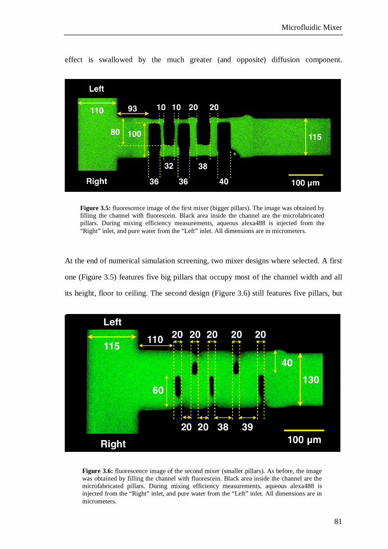
Microfluidic Mixer
81
effect is swallowed by the much greater (and opposite) diffusion component.
At the end of numerical simulation screening, two mixer designs where selected. A first
one (Figure 3.5) features five big pillars that occupy most of the channel width and all
its height, floor to ceiling. The second design (Figure 3.6) still features five pillars, but
Figure 3.6: fluorescence image of the second mixer (smaller pillars). As before, the image was obtained by filling the channel with fluorescein. Black area inside the channel are the microfabricated pillars. During mixing efficiency measurements, aqueous alexa488 is injected from the “Right” inlet, and pure water from the “Left” inlet. All dimensions are in micrometers.
Figure 3.5: fluorescence image of the first mixer (bigger pillars). The image was obtained by filling the channel with fluorescein. Black area inside the channel are the microfabricated pillars. During mixing efficiency measurements, aqueous alexa488 is injected from the “Right” inlet, and pure water from the “Left” inlet. All dimensions are in micrometers.
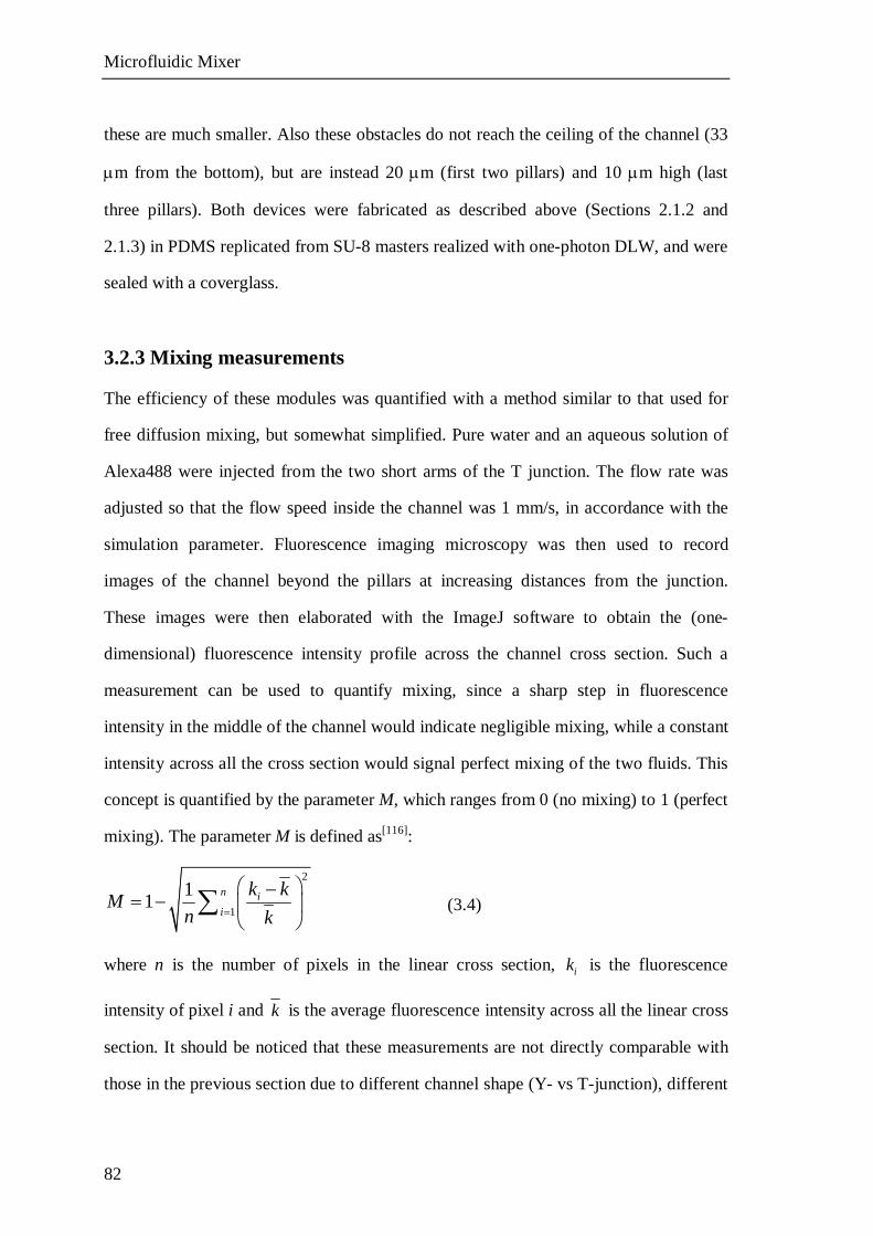
Microfluidic Mixer
82
these are much smaller. Also these obstacles do not reach the ceiling of the channel (33
m from the bottom), but are instead 20 m (first two pillars) and 10 m high (last
three pillars). Both devices were fabricated as described above (Sections 2.1.2 and
2.1.3) in PDMS replicated from SU-8 masters realized with one-photon DLW, and were
sealed with a coverglass.
3.2.3 Mixing measurements
The efficiency of these modules was quantified with a method similar to that used for
free diffusion mixing, but somewhat simplified. Pure water and an aqueous solution of
Alexa488 were injected from the two short arms of the T junction. The flow rate was
adjusted so that the flow speed inside the channel was 1 mm/s, in accordance with the
simulation parameter. Fluorescence imaging microscopy was then used to record
images of the channel beyond the pillars at increasing distances from the junction.
These images were then elaborated with the ImageJ software to obtain the (one-
dimensional) fluorescence intensity profile across the channel cross section. Such a
measurement can be used to quantify mixing, since a sharp step in fluorescence
intensity in the middle of the channel would indicate negligible mixing, while a constant
intensity across all the cross section would signal perfect mixing of the two fluids. This
concept is quantified by the parameter M, which ranges from 0 (no mixing) to 1 (perfect
mixing). The parameter M is defined as[116]:
2
1
11 n ii
k kMn k
(3.4)
where n is the number of pixels in the linear cross section, ik is the fluorescence
intensity of pixel i and k is the average fluorescence intensity across all the linear cross
section. It should be noticed that these measurements are not directly comparable with
those in the previous section due to different channel shape (Y- vs T-junction), different
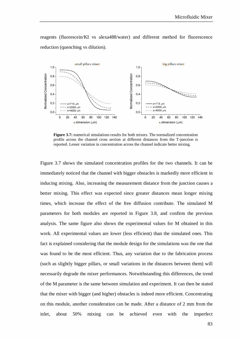
Microfluidic Mixer
83
reagents (fluorescein/KI vs alexa488/water) and different method for fluorescence
reduction (quenching vs dilution).
Figure 3.7 shows the simulated concentration profiles for the two channels. It can be
immediately noticed that the channel with bigger obstacles is markedly more efficient in
inducing mixing. Also, increasing the measurement distance from the junction causes a
better mixing. This effect was expected since greater distances mean longer mixing
times, which increase the effect of the free diffusion contribute. The simulated M
parameters for both modules are reported in Figure 3.8, and confirm the previous
analysis. The same figure also shows the experimental values for M obtained in this
work. All experimental values are lower (less efficient) than the simulated ones. This
fact is explained considering that the module design for the simulations was the one that
was found to be the most efficient. Thus, any variation due to the fabrication process
(such as slightly bigger pillars, or small variations in the distances between them) will
necessarily degrade the mixer performances. Notwithstanding this differences, the trend
of the M parameter is the same between simulation and experiment. It can then be stated
that the mixer with bigger (and higher) obstacles is indeed more efficient. Concentrating
on this module, another consideration can be made. After a distance of 2 mm from the
inlet, about 50% mixing can be achieved even with the imperfect
Figure 3.7: numerical simulations results for both mixers. The normalized concentration profile across the channel cross section at different distances from the T-junction is reported. Lesser variation in concentration across the channel indicate better mixing.
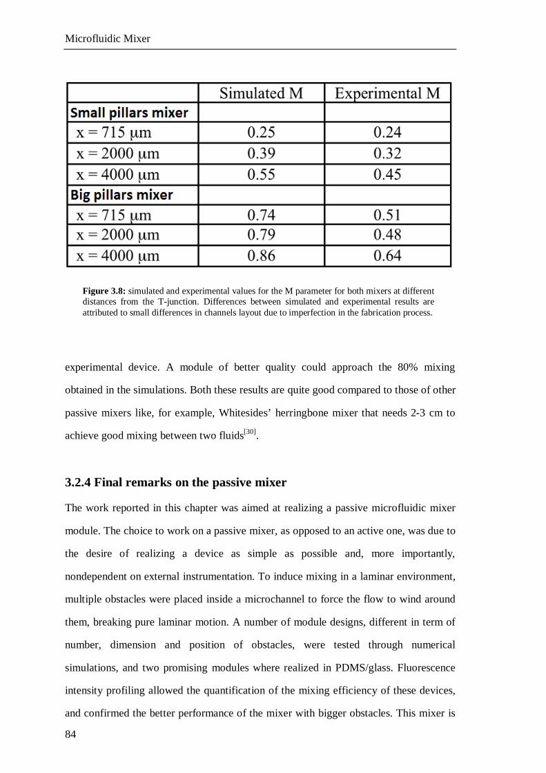
Microfluidic Mixer
84
experimental device. A module of better quality could approach the 80% mixing
obtained in the simulations. Both these results are quite good compared to those of other
passive mixers like, for example, Whitesides’ herringbone mixer that needs 2-3 cm to
achieve good mixing between two fluids[30].
3.2.4 Final remarks on the passive mixer
The work reported in this chapter was aimed at realizing a passive microfluidic mixer
module. The choice to work on a passive mixer, as opposed to an active one, was due to
the desire of realizing a device as simple as possible and, more importantly,
nondependent on external instrumentation. To induce mixing in a laminar environment,
multiple obstacles were placed inside a microchannel to force the flow to wind around
them, breaking pure laminar motion. A number of module designs, different in term of
number, dimension and position of obstacles, were tested through numerical
simulations, and two promising modules where realized in PDMS/glass. Fluorescence
intensity profiling allowed the quantification of the mixing efficiency of these devices,
and confirmed the better performance of the mixer with bigger obstacles. This mixer is
Figure 3.8: simulated and experimental values for the M parameter for both mixers at different distances from the T-junction. Differences between simulated and experimental results are attributed to small differences in channels layout due to imperfection in the fabrication process.

Microfluidic Mixer
85
highly efficient regardless of the quite simple design and production technique, and
without the need for any additional equipment can be readily added to any modular
MFD that requires a mixing functionality.

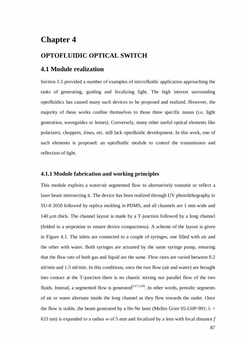
87
Chapter 4
OPTOFLUIDIC OPTICAL SWITCH
4.1 Module realization
Section 1.5 provided a number of examples of microfluidic application approaching the
tasks of generating, guiding and focalizing light. The high interest surrounding
optofluidics has caused many such devices to be proposed and realized. However, the
majority of these works confine themselves to those three specific issues (i.e. light
generation, waveguides or lenses). Conversely, many other useful optical elements like
polarizers, choppers, irises, etc. still lack optofluidic development. In this work, one of
such elements is proposed: an optofluidic module to control the transmission and
reflection of light.
4.1.1 Module fabrication and working principles
This module exploits a water/air segmented flow to alternatively transmit or reflect a
laser beam intersecting it. The device has been realized through UV photolithography in
SU-8 2050 followed by replica molding in PDMS, and all channels are 1 mm wide and
140 m thick. The channel layout is made by a T-junction followed by a long channel
(folded in a serpentine to ensure device compactness). A scheme of the layout is given
in Figure 4.1. The inlets are connected to a couple of syringes, one filled with air and
the other with water. Both syringes are actuated by the same syringe pump, ensuring
that the flow rate of both gas and liquid are the same. Flow rates are varied between 0.2
ml/min and 1.5 ml/min. In this conditions, once the two flow (air and water) are brought
into contact at the T-junction there is no chaotic mixing nor parallel flow of the two
fluids. Instead, a segmented flow is generated[117,118]. In other words, periodic segments
of air or water alternate inside the long channel as they flow towards the outlet. Once
the flow is stable, the beam generated by a He-Ne laser (Melles Griot 05-LHP-991; =
633 nm) is expanded to a radius w of 5 mm and focalized by a lens with focal distance f
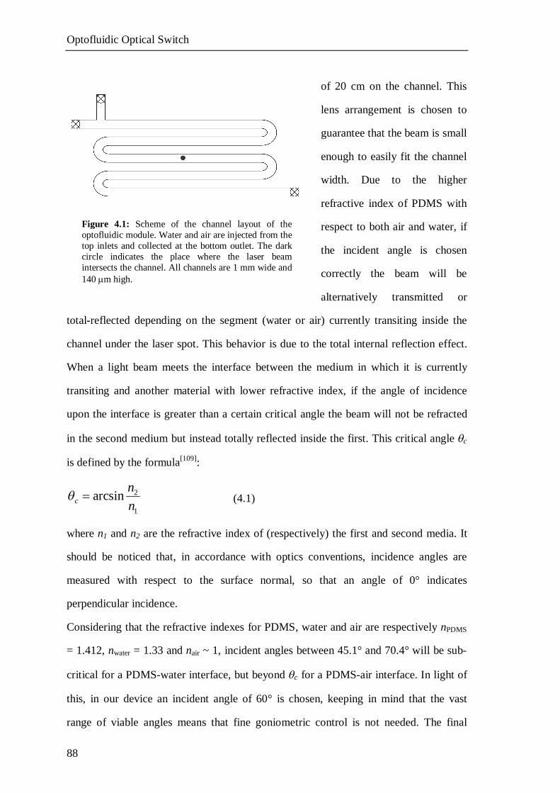
Optofluidic Optical Switch
88
of 20 cm on the channel. This
lens arrangement is chosen to
guarantee that the beam is small
enough to easily fit the channel
width. Due to the higher
refractive index of PDMS with
respect to both air and water, if
the incident angle is chosen
correctly the beam will be
alternatively transmitted or
total-reflected depending on the segment (water or air) currently transiting inside the
channel under the laser spot. This behavior is due to the total internal reflection effect.
When a light beam meets the interface between the medium in which it is currently
transiting and another material with lower refractive index, if the angle of incidence
upon the interface is greater than a certain critical angle the beam will not be refracted
in the second medium but instead totally reflected inside the first. This critical angle c
is defined by the formula[109]:
2
1
arcsincnn
(4.1)
where n1 and n2 are the refractive index of (respectively) the first and second media. It
should be noticed that, in accordance with optics conventions, incidence angles are
measured with respect to the surface normal, so that an angle of 0° indicates
perpendicular incidence.
Considering that the refractive indexes for PDMS, water and air are respectively nPDMS
= 1.412, nwater = 1.33 and nair ~ 1, incident angles between 45.1° and 70.4° will be sub-
critical for a PDMS-water interface, but beyond c for a PDMS-air interface. In light of
this, in our device an incident angle of 60° is chosen, keeping in mind that the vast
range of viable angles means that fine goniometric control is not needed. The final
Figure 4.1: Scheme of the channel layout of the optofluidic module. Water and air are injected from the top inlets and collected at the bottom outlet. The dark circle indicates the place where the laser beam intersects the channel. All channels are 1 mm wide and 140 m high.
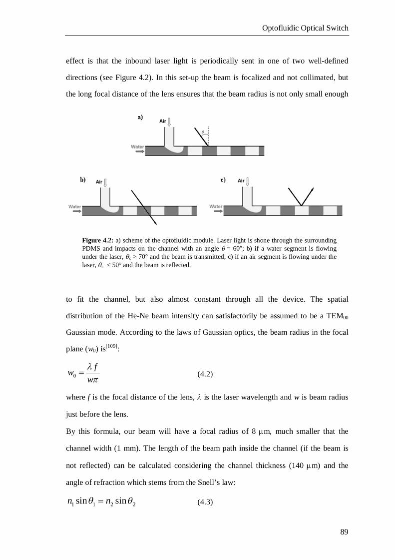
Optofluidic Optical Switch
89
effect is that the inbound laser light is periodically sent in one of two well-defined
directions (see Figure 4.2). In this set-up the beam is focalized and not collimated, but
the long focal distance of the lens ensures that the beam radius is not only small enough
to fit the channel, but also almost constant through all the device. The spatial
distribution of the He-Ne beam intensity can satisfactorily be assumed to be a TEM00
Gaussian mode. According to the laws of Gaussian optics, the beam radius in the focal
plane (w0) is[109]:
0fw
w
(4.2)
where f is the focal distance of the lens, is the laser wavelength and w is beam radius
just before the lens.
By this formula, our beam will have a focal radius of 8 m, much smaller that the
channel width (1 mm). The length of the beam path inside the channel (if the beam is
not reflected) can be calculated considering the channel thickness (140 m) and the
angle of refraction which stems from the Snell’s law:
1 1 2 2sin sinn n (4.3)
Figure 4.2: a) scheme of the optofluidic module. Laser light is shone through the surrounding PDMS and impacts on the channel with an angle = 60°; b) if a water segment is flowing under the laser, c > 70° and the beam is transmitted; c) if an air segment is flowing under the laser, c < 50° and the beam is reflected.
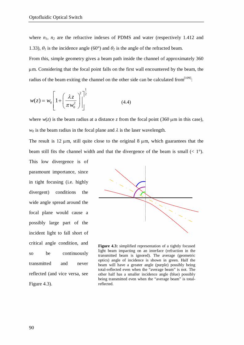
Optofluidic Optical Switch
90
where n1, n2 are the refractive indexes of PDMS and water (respectively 1.412 and
1.33), 1 is the incidence angle (60°) and 2 is the angle of the refracted beam.
From this, simple geometry gives a beam path inside the channel of approximately 360
m. Considering that the focal point falls on the first wall encountered by the beam, the
radius of the beam exiting the channel on the other side can be calculated from[109]:
12 2
0 20
( ) 1 zw z ww
(4.4)
where w(z) is the beam radius at a distance z from the focal point (360 m in this case),
w0 is the beam radius in the focal plane and is the laser wavelength.
The result is 12 m, still quite close to the original 8 m, which guarantees that the
beam still fits the channel width and that the divergence of the beam is small (< 1°).
This low divergence is of
paramount importance, since
in tight focusing (i.e. highly
divergent) conditions the
wide angle spread around the
focal plane would cause a
possibly large part of the
incident light to fall short of
critical angle condition, and
so be continuously
transmitted and never
reflected (and vice versa, see
Figure 4.3).
Figure 4.3: simplified representation of a tightly focused light beam impacting on an interface (refraction in the transmitted beam is ignored). The average (geometric optics) angle of incidence is shown in green. Half the beam will have a greater angle (purple) possibly being total-reflected even when the “average beam” is not. The other half has a smaller incidence angle (blue) possibly being transmitted even when the “average beam” is total-reflected.
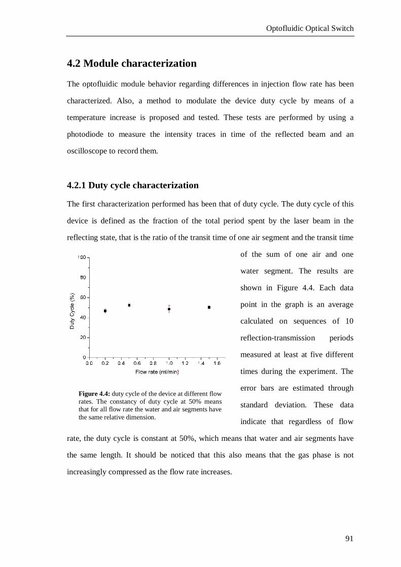
Optofluidic Optical Switch
91
4.2 Module characterization
The optofluidic module behavior regarding differences in injection flow rate has been
characterized. Also, a method to modulate the device duty cycle by means of a
temperature increase is proposed and tested. These tests are performed by using a
photodiode to measure the intensity traces in time of the reflected beam and an
oscilloscope to record them.
4.2.1 Duty cycle characterization
The first characterization performed has been that of duty cycle. The duty cycle of this
device is defined as the fraction of the total period spent by the laser beam in the
reflecting state, that is the ratio of the transit time of one air segment and the transit time
of the sum of one air and one
water segment. The results are
shown in Figure 4.4. Each data
point in the graph is an average
calculated on sequences of 10
reflection-transmission periods
measured at least at five different
times during the experiment. The
error bars are estimated through
standard deviation. These data
indicate that regardless of flow
rate, the duty cycle is constant at 50%, which means that water and air segments have
the same length. It should be noticed that this also means that the gas phase is not
increasingly compressed as the flow rate increases.
Figure 4.4: duty cycle of the device at different flow rates. The constancy of duty cycle at 50% means that for all flow rate the water and air segments have the same relative dimension.
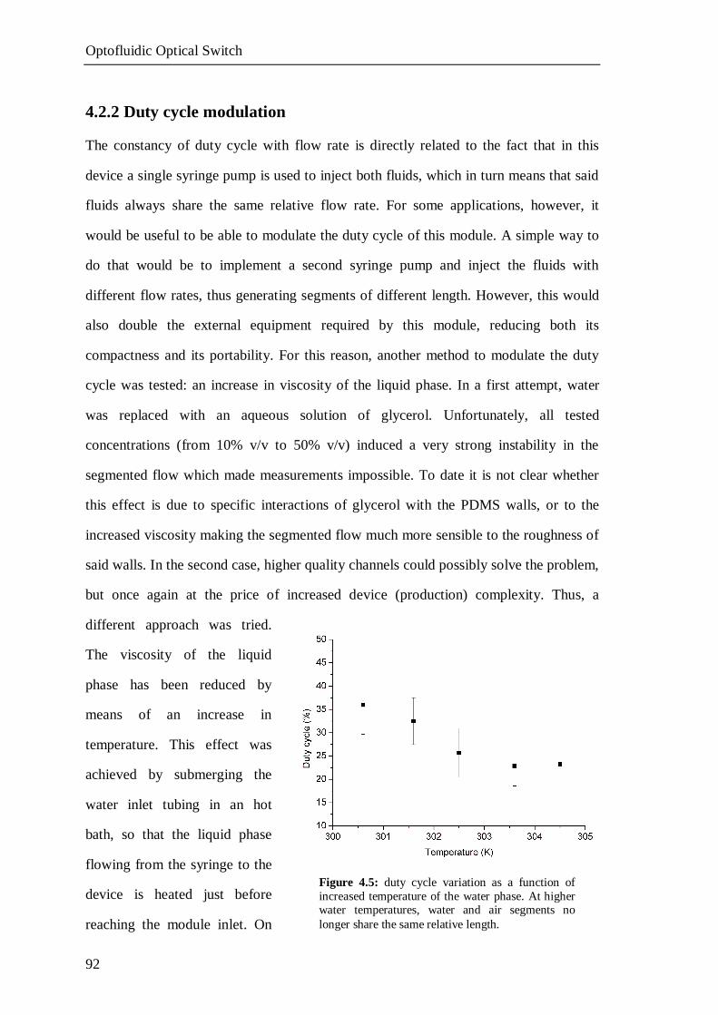
Optofluidic Optical Switch
92
4.2.2 Duty cycle modulation
The constancy of duty cycle with flow rate is directly related to the fact that in this
device a single syringe pump is used to inject both fluids, which in turn means that said
fluids always share the same relative flow rate. For some applications, however, it
would be useful to be able to modulate the duty cycle of this module. A simple way to
do that would be to implement a second syringe pump and inject the fluids with
different flow rates, thus generating segments of different length. However, this would
also double the external equipment required by this module, reducing both its
compactness and its portability. For this reason, another method to modulate the duty
cycle was tested: an increase in viscosity of the liquid phase. In a first attempt, water
was replaced with an aqueous solution of glycerol. Unfortunately, all tested
concentrations (from 10% v/v to 50% v/v) induced a very strong instability in the
segmented flow which made measurements impossible. To date it is not clear whether
this effect is due to specific interactions of glycerol with the PDMS walls, or to the
increased viscosity making the segmented flow much more sensible to the roughness of
said walls. In the second case, higher quality channels could possibly solve the problem,
but once again at the price of increased device (production) complexity. Thus, a
different approach was tried.
The viscosity of the liquid
phase has been reduced by
means of an increase in
temperature. This effect was
achieved by submerging the
water inlet tubing in an hot
bath, so that the liquid phase
flowing from the syringe to the
device is heated just before
reaching the module inlet. On
Figure 4.5: duty cycle variation as a function of increased temperature of the water phase. At higher water temperatures, water and air segments no longer share the same relative length.
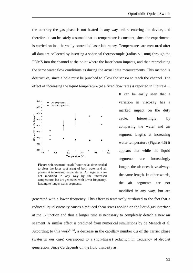
Optofluidic Optical Switch
93
the contrary the gas phase is not heated in any way before entering the device, and
therefore it can be safely assumed that its temperature is constant, since the experiments
is carried on in a thermally controlled laser laboratory. Temperatures are measured after
all data are collected by inserting a spherical thermocouple (radius < 1 mm) through the
PDMS into the channel at the point where the laser beam impacts, and then reproducing
the same water flow conditions as during the actual data measurements. This method is
destructive, since a hole must be punched to allow the sensor to reach the channel. The
effect of increasing the liquid temperature (at a fixed flow rate) is reported in Figure 4.5.
It can be easily seen that a
variation in viscosity has a
marked impact on the duty
cycle. Interestingly, by
comparing the water and air
segment lengths at increasing
water temperature (Figure 4.6) it
appears that while the liquid
segments are increasingly
longer, the air ones have always
the same length. In other words,
the air segments are not
modified in any way, but are
generated with a lower frequency. This effect is tentatively attributed to the fact that a
reduced liquid viscosity causes a reduced shear stress applied on the liquid/gas interface
at the T-junction and thus a longer time is necessary to completely detach a new air
segment. A similar effect is predicted from numerical simulations by de Menech et al.
According to this work[119], a decrease in the capillary number Ca of the carrier phase
(water in our case) correspond to a (non-linear) reduction in frequency of droplet
generation. Since Ca depends on the fluid viscosity as:
Figure 4.6: segment length (reported as time needed to clear the laser spot area) of both water and air phases at increasing temperatures. Air segments are not modified in any way by the increased temperature, but are generated with lower frequency, leading to longer water segments.
Optofluidic Optical Switch
94
vCa
(4.5)
where is the dynamic viscosity of the fluid, v its velocity and the interfacial tension
between the two phases, our results are in accordance with these predictions. However,
it should be noticed that de Menech’s work treated a liquid/liquid system, as opposed to
the liquid/gas one proposed here. Also, a number of published results[119–121], both
theoretical and experimental, show that a reduced generation frequency should be
matched by the generation of progressively longer segments for both fluids, a result that
we did not observe, possibly due to differences in channels geometry.
From Figures 4.5 and 4.6 it can be seen that the experiments with increased
temperatures feature a noticeably lower reproducibility compared with those at room
temperature. This is likely caused by the fact that water has been heated just before
being introduced in the device, but considering the very large surface/volume ratio
inside the microchannels it is inevitable that a gradient in liquid temperature will be
generated inside the module. This gradient is a source of instability that degrades the
reproducibility properties of the experiment. Another remarkable point is that while a
relatively small change in liquid temperature will cause a variation of the duty cycle,
during the previous room temperature experiments the 50% duty cycle shown in Figure
4.4 was nonetheless highly reproducible for long times (up to 90 minutes). This can be
explained considering two facts. First of all, all experiments are performed in a
thermally controlled laser laboratory with variations in room temperature not exceeding
2 K. Secondarily, PDMS is a very poor heat conductor. As such, it takes a long time
for a slight increase in room temperature to actually increase the temperature inside the
device, under several millimeters of PDMS. A similar reasoning can be made for the
water reservoir that provides the liquid for the device, since water itself is a quite poor
heat conductor. These properties help to dampen the temperature fluctuation that can
happen during the experiment, and can be extremely advantageous if the device is to be
used “on the field”. The measurements at increasing temperatures have been repeated
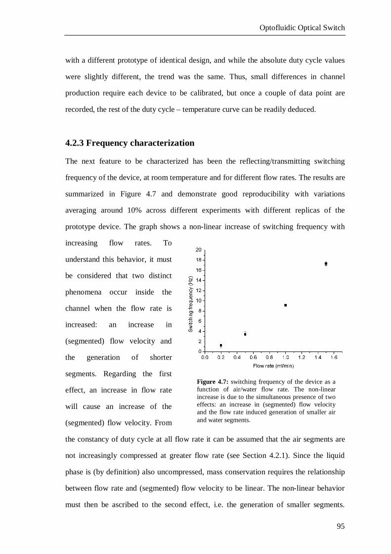
Optofluidic Optical Switch
95
with a different prototype of identical design, and while the absolute duty cycle values
were slightly different, the trend was the same. Thus, small differences in channel
production require each device to be calibrated, but once a couple of data point are
recorded, the rest of the duty cycle – temperature curve can be readily deduced.
4.2.3 Frequency characterization
The next feature to be characterized has been the reflecting/transmitting switching
frequency of the device, at room temperature and for different flow rates. The results are
summarized in Figure 4.7 and demonstrate good reproducibility with variations
averaging around 10% across different experiments with different replicas of the
prototype device. The graph shows a non-linear increase of switching frequency with
increasing flow rates. To
understand this behavior, it must
be considered that two distinct
phenomena occur inside the
channel when the flow rate is
increased: an increase in
(segmented) flow velocity and
the generation of shorter
segments. Regarding the first
effect, an increase in flow rate
will cause an increase of the
(segmented) flow velocity. From
the constancy of duty cycle at all flow rate it can be assumed that the air segments are
not increasingly compressed at greater flow rate (see Section 4.2.1). Since the liquid
phase is (by definition) also uncompressed, mass conservation requires the relationship
between flow rate and (segmented) flow velocity to be linear. The non-linear behavior
must then be ascribed to the second effect, i.e. the generation of smaller segments.
Figure 4.7: switching frequency of the device as a function of air/water flow rate. The non-linear increase is due to the simultaneous presence of two effects: an increase in (segmented) flow velocity and the flow rate induced generation of smaller air and water segments.
Optofluidic Optical Switch
96
While this effect can be clearly seen experimentally, this component is difficult to
model, and so channels with different geometries will have to be experimentally
calibrated.
Regardless of the quite simple production processes used to fabricate this module, the
device features a very good stability in time for flow rates up to 1.5 ml/min. In these
conditions the capacity of the employed syringes is usually the limiting factor for
maximum measurement time. At very high flow rates (greater than 2 ml/min) the
segmented flow becomes unstable after a few minutes. This is likely caused by the
microscopic roughness of the channel walls, that becomes critical at high flow
velocities. Literature evidences[122,123] suggests that this problem could be mitigated (if
not outright solved) by fabricating higher quality devices or by functionalizing the
channels interiors, but as before these improvements would be to the detriment of
production simplicity. Moreover, flow rates up to 1.5 ml min-1, corresponding to a
switching frequency of almost 18 Hz, have been deemed sufficient for most
applications. Considering (as an example) a device for recording light absorption
spectra which uses this module to implement a two beam geometry with 0.5 nm spectral
resolution, a switching frequency of 10 Hz (equal to a flow rate of 1 ml/min, well below
the device limit) would be enough to achieve a scanning speed of 300 nm/min, which is
a typical value for commercial, macroscopic spectrophotometers.
4.2.4 Final remarks on the optofluidic light switch
In this chapter an optofluidic module for the control of light has been proposed and
characterized. This device exploits a segmented flow to alternatively and periodically
transmit or reflect a laser beam shone on the channel. The frequency of operation
depends only on the liquid/air flow rate, and thus can be easily controlled. Also, a
variation in liquid phase viscosity can be used to tune the duty cycle of the device.
While the construction process is very simple, the device response is reproducible. If
greater stability becomes a requirements, additional processes can be implemented (like
Optofluidic Optical Switch
97
channel functionalization) by partially sacrificing ease of production. This module is
quite straightforward in its use, and requires minimal external equipment, making it a
good candidate for inclusion in any modular optofluidic arrangement that currently lack
a light switching or chopping functionality. This module can also work as a sort of
beam splitter that, instead of dividing the total energy of the inbound beam, sends all the
available energy alternatively (and periodically) toward one direction or the other. This
particular feature can be extremely beneficial for applications where the available light
power is low, as is typically the case for MFDs where the light is generated on-chip.

99
Chapter 5
WATER-CORE PDMS WAVEGUIDE
5.1 Porous PDMS claddings
The importance of waveguiding light inside microfluidic devices has already been
mentioned in Section 1.5.4, in particular concerning the possibility of making the fluid-
carrying microchannels double as waveguides. This arrangement would not only allow
a reduction of the physical dimensions of the involved modules, but also (and more
importantly) guarantee long interaction paths between fluid and light. Unfortunately, the
typical MFD bulk materials (PDMS and glass) feature a greater refractive index than the
fluid commonly carried inside the device (i.e. water). This means that microchannels
cannot usually work as conventional, total-reflection-confined waveguides, and other
strategies must be implemented.
5.1.1 Limits of existing liquid-core waveguides
Two of the most common optofluidic waveguides, ARROWs and L2, have been
described in Section 1.5.4. Both these strategies have been successfully employed, but
suffer also from some limitation. Starting with ARROWs, antiresonant reflecting optical
waveguides are quite efficient in keeping the light in the channel, but require very fine
micro- or nanofabrication methods to precisely tune the thickness of the layer providing
the antiresonant effect. Moreover, these guides require the integration of at least two
different materials. This fact not only complicates the design of the involved modules,
but if the second material is not elastic, it also hampers the deformation capabilities of
PDMS modules. Considering that a great number of tunable MFDs achieve tunability
thanks to said deformations (see Sections 1.5.3 and 1.5.5), this last drawback is non-
negligible. The second kind of guiding geometry, L2 waveguides, doesn’t have the strict
fabrication requirements of ARROWs, but still present limitations. First of all, since the
guiding flow is usually stratified and not annular, light is confined only in one
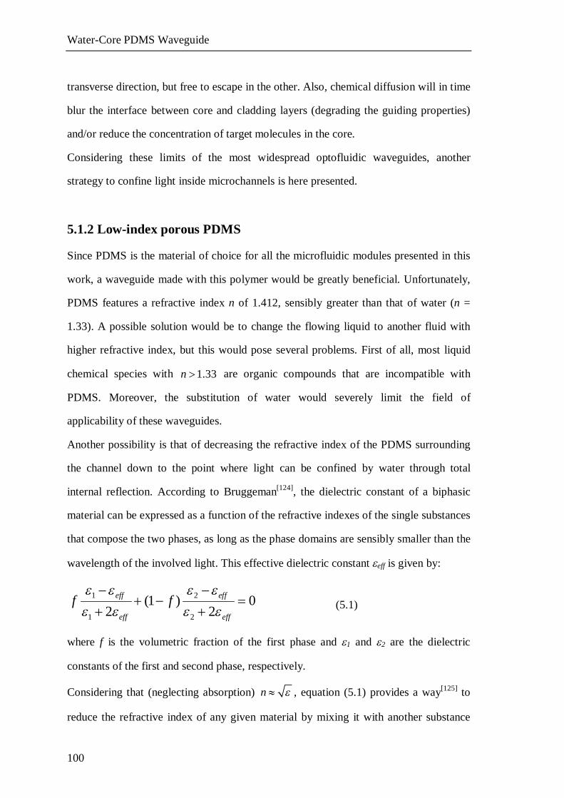
Water-Core PDMS Waveguide
100
transverse direction, but free to escape in the other. Also, chemical diffusion will in time
blur the interface between core and cladding layers (degrading the guiding properties)
and/or reduce the concentration of target molecules in the core.
Considering these limits of the most widespread optofluidic waveguides, another
strategy to confine light inside microchannels is here presented.
5.1.2 Low-index porous PDMS
Since PDMS is the material of choice for all the microfluidic modules presented in this
work, a waveguide made with this polymer would be greatly beneficial. Unfortunately,
PDMS features a refractive index n of 1.412, sensibly greater than that of water (n =
1.33). A possible solution would be to change the flowing liquid to another fluid with
higher refractive index, but this would pose several problems. First of all, most liquid
chemical species with 1.33n are organic compounds that are incompatible with
PDMS. Moreover, the substitution of water would severely limit the field of
applicability of these waveguides.
Another possibility is that of decreasing the refractive index of the PDMS surrounding
the channel down to the point where light can be confined by water through total
internal reflection. According to Bruggeman[124], the dielectric constant of a biphasic
material can be expressed as a function of the refractive indexes of the single substances
that compose the two phases, as long as the phase domains are sensibly smaller than the
wavelength of the involved light. This effective dielectric constant eff is given by:
1 2
1 2
(1 ) 02 2
eff eff
eff eff
f f
(5.1)
where f is the volumetric fraction of the first phase and 1 and 2 are the dielectric
constants of the first and second phase, respectively.
Considering that (neglecting absorption) n , equation (5.1) provides a way[125] to
reduce the refractive index of any given material by mixing it with another substance
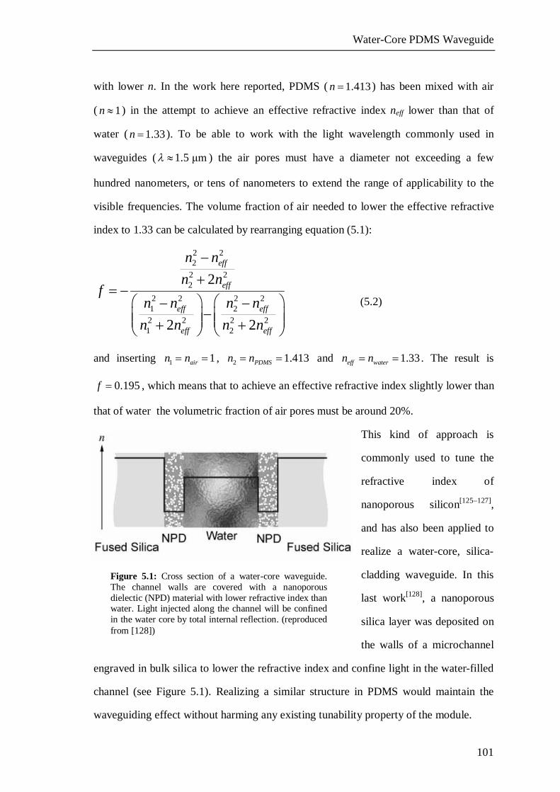
Water-Core PDMS Waveguide
101
with lower n. In the work here reported, PDMS ( 1.413n ) has been mixed with air
( 1n ) in the attempt to achieve an effective refractive index neff lower than that of
water ( 1.33n ). To be able to work with the light wavelength commonly used in
waveguides ( 1.5 μm ) the air pores must have a diameter not exceeding a few
hundred nanometers, or tens of nanometers to extend the range of applicability to the
visible frequencies. The volume fraction of air needed to lower the effective refractive
index to 1.33 can be calculated by rearranging equation (5.1):
2 22
2 22
2 2 2 21 22 2 2 21 2
2
2 2
eff
eff
eff eff
eff eff
n nn n
fn n n n
n n n n
(5.2)
and inserting 1 1airn n , 2 1.413PDMSn n and 1.33eff watern n . The result is
0.195f , which means that to achieve an effective refractive index slightly lower than
that of water the volumetric fraction of air pores must be around 20%.
This kind of approach is
commonly used to tune the
refractive index of
nanoporous silicon[125–127],
and has also been applied to
realize a water-core, silica-
cladding waveguide. In this
last work[128], a nanoporous
silica layer was deposited on
the walls of a microchannel
engraved in bulk silica to lower the refractive index and confine light in the water-filled
channel (see Figure 5.1). Realizing a similar structure in PDMS would maintain the
waveguiding effect without harming any existing tunability property of the module.
Figure 5.1: Cross section of a water-core waveguide. The channel walls are covered with a nanoporous dielectic (NPD) material with lower refractive index than water. Light injected along the channel will be confined in the water core by total internal reflection. (reproduced from [128])
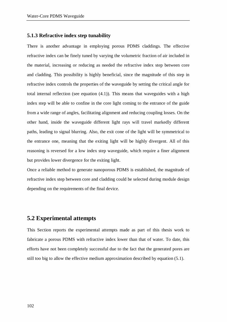
Water-Core PDMS Waveguide
102
5.1.3 Refractive index step tunability
There is another advantage in employing porous PDMS claddings. The effective
refractive index can be finely tuned by varying the volumetric fraction of air included in
the material, increasing or reducing as needed the refractive index step between core
and cladding. This possibility is highly beneficial, since the magnitude of this step in
refractive index controls the properties of the waveguide by setting the critical angle for
total internal reflection (see equation (4.1)). This means that waveguides with a high
index step will be able to confine in the core light coming to the entrance of the guide
from a wide range of angles, facilitating alignment and reducing coupling losses. On the
other hand, inside the waveguide different light rays will travel markedly different
paths, leading to signal blurring. Also, the exit cone of the light will be symmetrical to
the entrance one, meaning that the exiting light will be highly divergent. All of this
reasoning is reversed for a low index step waveguide, which require a finer alignment
but provides lower divergence for the exiting light.
Once a reliable method to generate nanoporous PDMS is established, the magnitude of
refractive index step between core and cladding could be selected during module design
depending on the requirements of the final device.
5.2 Experimental attempts
This Section reports the experimental attempts made as part of this thesis work to
fabricate a porous PDMS with refractive index lower than that of water. To date, this
efforts have not been completely successful due to the fact that the generated pores are
still too big to allow the effective medium approximation described by equation (5.1).
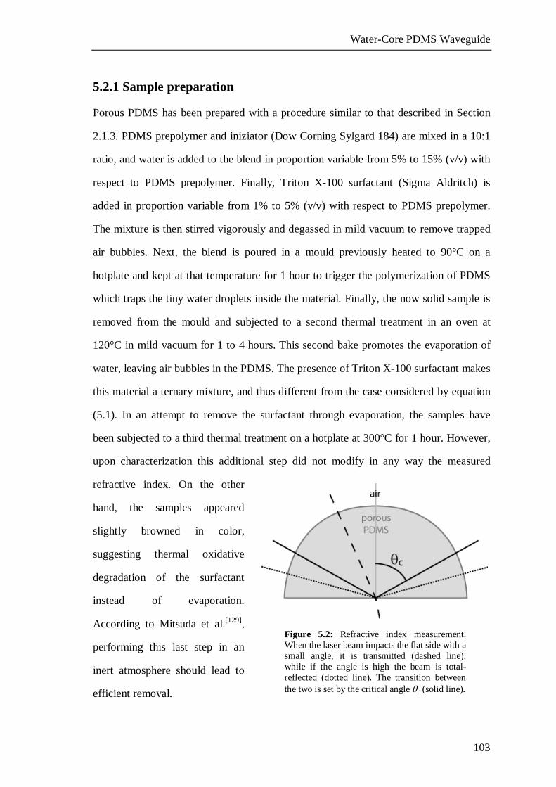
Water-Core PDMS Waveguide
103
5.2.1 Sample preparation
Porous PDMS has been prepared with a procedure similar to that described in Section
2.1.3. PDMS prepolymer and iniziator (Dow Corning Sylgard 184) are mixed in a 10:1
ratio, and water is added to the blend in proportion variable from 5% to 15% (v/v) with
respect to PDMS prepolymer. Finally, Triton X-100 surfactant (Sigma Aldritch) is
added in proportion variable from 1% to 5% (v/v) with respect to PDMS prepolymer.
The mixture is then stirred vigorously and degassed in mild vacuum to remove trapped
air bubbles. Next, the blend is poured in a mould previously heated to 90°C on a
hotplate and kept at that temperature for 1 hour to trigger the polymerization of PDMS
which traps the tiny water droplets inside the material. Finally, the now solid sample is
removed from the mould and subjected to a second thermal treatment in an oven at
120°C in mild vacuum for 1 to 4 hours. This second bake promotes the evaporation of
water, leaving air bubbles in the PDMS. The presence of Triton X-100 surfactant makes
this material a ternary mixture, and thus different from the case considered by equation
(5.1). In an attempt to remove the surfactant through evaporation, the samples have
been subjected to a third thermal treatment on a hotplate at 300°C for 1 hour. However,
upon characterization this additional step did not modify in any way the measured
refractive index. On the other
hand, the samples appeared
slightly browned in color,
suggesting thermal oxidative
degradation of the surfactant
instead of evaporation.
According to Mitsuda et al.[129],
performing this last step in an
inert atmosphere should lead to
efficient removal.
Figure 5.2: Refractive index measurement. When the laser beam impacts the flat side with a small angle, it is transmitted (dashed line), while if the angle is high the beam is total-reflected (dotted line). The transition between the two is set by the critical angle c (solid line).
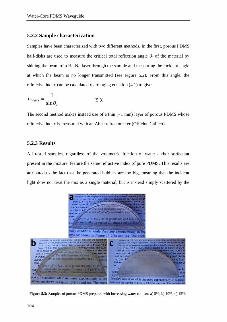
Water-Core PDMS Waveguide
104
5.2.2 Sample characterization
Samples have been characterized with two different methods. In the first, porous PDMS
half-disks are used to measure the critical total reflection angle c of the material by
shining the beam of a He-Ne laser through the sample and measuring the incident angle
at which the beam is no longer transmitted (see Figure 5.2). From this angle, the
refractive index can be calculated rearranging equation (4.1) to give:
1sinPDMS
c
n
(5.3)
The second method makes instead use of a thin (~1 mm) layer of porous PDMS whose
refractive index is measured with an Abbe refractometer (Officine Galileo).
5.2.3 Results
All tested samples, regardless of the volumetric fraction of water and/or surfactant
present in the mixture, feature the same refractive index of pure PDMS. This results are
attributed to the fact that the generated bubbles are too big, meaning that the incident
light does not treat the mix as a single material, but is instead simply scattered by the
Figure 5.3: Samples of porous PDMS prepared with increasing water content: a) 5%; b) 10%; c) 15%.
Water-Core PDMS Waveguide
105
pores. Supporting this explanation is the fact that all samples appear opaque under white
light, and the opacity increases with increasing water content (see Figure 5.3). This
appearance suggests that the air bubbles inside the PDMS have a diameter on the order
of hundreds of nanometers to a few micrometers, so to efficiently scatter visible light.
The difficulty in obtaining small pores is related to the hydrophobicity of PDMS, which
makes the generation of small water droplets strongly energetically unfavorable, even
when a surfactant is added to the mix. This limit can be mitigated by using a different,
more affine, species as templating liquid. Unfortunately, a too strong affinity will
usually translate in actual mixing between liquid and (unpolymerized) PDMS,
preventing the formation of two distinct phases. Thus, a balance must be stroke so that
droplets are formed, but the surface energy between the two phases is low enough to
keep the emulsion stable until PDMS polymerization.
Following this reasoning, an attempt was made to substitute water with acetonitrile. An
emulsion was formed with unpolymerized PDMS as described in Section 5.2.1 except
for the first bake temperature that was reduced to 70°C to prevent acetonitrile from
boiling. The resulting samples show a noticeable degrade in terms of elasticity and
appear not completely polymerized even after several days, probably due to unfavorable
interactions between acetonitrile and PDMS. Moreover, the refractive index was still
that of pure PDMS.
5.2.4 Future prospects
Future experiments concerning this part of the work will concentrate on the
identification of a suitable templating fluid to generate nanometric pores in PDMS.
Also, different surfactants and will be tested, as well as different processes to generate
the initial emulsion. If a porous material of suitable refractive index can be generated,
liquid-core waveguides will be tested by depositing a thin layer of this material on the
inside walls of a microchannel engraved in bulk PDMS. While this will bring the porous

Water-Core PDMS Waveguide
106
material in direct contact with the flowing water, it is expected that the hydrophobicity
of PDMS will inhibit the fluid from entering the nanometric pores.
107
Conclusions
The work in this thesis was aimed at the realization of single-function modules ready
for inclusion into modular microfluidic devices (MFDs). The rationale behind this aim
in that once a suitable collection of different modules has been created, MFDs for a
great number of different applications can be realized by simply combining the modules
that carry out the required functionalities.
The modules have been realized through PDMS replica molding, a well-established
technique frequently employed in literature. The masters to be replicated have been
realized in the commercial photoresist SU-8 with masked UV photolithography or direct
laser writing (DLW). While UV-photolithography is a fast method to structure large
areas, the better resolution of DLW allows the realization of smaller features. This
benefit is further enhanced by the employment of laser writing mediated by two-photon
processes, since the strong dependency of non-linear absorption on incident light
intensity allows a very fine control on the photopolymerization process.
The use of PDMS as bulk material for microdevices has several advantages, including
optical transparency, good resistance to water and a marked elasticity that facilitate the
detachment of the PDMS replica from the SU-8 master. Unfortunately, this same
elasticity also causes some limitations on the shapes that can be created, since high
aspect ratio structures will usually collapse under their own weight. For this reason, a
new photopolymerizable hybrid organic/inorganic sol-gel material was proposed and
characterized. This blend has better mechanical properties and chemical resistance than
PDMS. It also allows two-photon DLW with good resolution (down to 600 nm), and
shows a clear relation between diameter of the polymerized area, exposure time and
laser power. However, results from different batches of the same blend are only
reproducible within ~500 nm, so if submicrometric resolutions are required, the exact
response of each batch of material will have to be calibrated before use. Another
limiting factor of this sol-gel blend is that, while its hybrid nature confers it a reduced
Conclusions
108
stiffness compared to fully inorganic materials, still the shrinkage occurring during
polymerization produces cracks in structures with more than one dimension exceeding
1-2 m. This limit translates into the fact that this blend cannot be used as bulk material
for MFDs, but it is an excellent candidate for the realization of specific internal sub-
structurations that PDMS cannot replicate. To extend the field of applicability of this
material, the biocompatibility of flat, fully polymerized sol-gel substrates was tested by
growing primary HUVEC cells and comparing their proliferation to that of a control
sample grown on a glass substrate. The results confirmed the biocompatibility of this
blend, but also revealed another potential problem. Even for the fully polymerized
material, a small fraction of the photoinitiator remains unreacted. This species is
fluorescent in a range overlapping that of some fluorescent labels commonly used in
biology-related work (mainly DAPI and BrdU). This means that a number of typical
tests performed on this substrate will suffer from a diffuse background that will degrade
the signal to noise ratio of the measurement.
The first microfluidic module that has been realized is a mixer. Fluids inside
micrometric channel are subjected to laminar conditions, i.e. their vectorial velocity has
only one component, parallel to the channel axis. This means that two different miscible
liquids brought into contact inside a microchannel will only mix through chemical
diffusion, a slow process compared to the residence time of the fluid inside the MFD.
To increase the mixing efficiency, and thus the time required to blend the different
fluids, specific microfluidic elements must be designed. In this work one such element
was realized by inserting multiple obstructions inside a microchannel to locally perturb
the laminar conditions and thus favor mixing. A preliminary screening of different
designs was performed by means of numerical simulations, and two promising layouts
were tested experimentally. To quantify the mixing efficiency, a fluorophore solution
and pure solvent were injected in the upper arms of a T-shaped channel and brought into
contact at the junction. Fluorescence intensity profiles were recorded across the channel
at different distances from the junction and the degree of mixing was estimated
Conclusions
109
considering a flat, uniform intensity profile as 100% and a vertical drop from maximum
to zero as 0%. The results were in good agreement with the simulation predictions, and
demonstrated that the channel with bigger and higher obstacles was the most efficient.
Slight deviations of the measured mixing efficiencies from the simulated ones were
attributed to fabrication imperfections.
The second microfluidic module that has been realized is a light switch for optofluidic
applications. This device exploits a water/air segmented flow to alternatively transmit
and reflect a laser beam incident on the channel. This behavior is due to the difference
in refractive index between the two fluids composing the segmented flow. For the
selected light incidence angle (60°), the refractive index of air triggers total internal
reflection inside the bulk PDMS that surrounds the channel, preventing the light from
being transmitted. On the contrary, the higher refractive index of water is too similar to
that of PDMS to achieve the same phenomenon, and the light can pass through the
channel. The result is a periodic deflection of the inbound laser towards one of two
well-defined directions. The duty cycle of the device (the fraction of the total period
spent by the laser beam in the reflected state), was found to be constant at 50% for all
tested injection flow rates. Since some applications would benefit from a variable duty
cycle, a method for its modulation was proposed and tested: an increase in the water
phase temperature. This method proved effective, causing a reproducible decrease in
duty cycle from 50% to 25% with a temperature variation of less than 10 K. The
dependency of the switching frequency of the device on injection flow rate was also
characterized, and showed a nonlinear increase at higher flow rates. This effect was
attributed both to the faster movement of segments inside the channel and to the
generation of shorter segments at higher flow rates. Notwithstanding the simple design
and realization of this device, the module proved to be stable for very long times for
flow rates up to 1.5 ml/min. It is probable that higher flow rates could be supported if
the fabrication technique was improved to achieve better quality channels. However,
Conclusions
110
flow rates up to 1.5 ml/min have been deemed sufficient for most applications, and so to
preserve ease of fabrication this further modifications were not explored.
Finally, a number of attempts to realize a nanoporous, low refractive index PDMS have
been reported. Water and a surfactant have been mixed to unpolymerized PDMS and
forced to generate an emulsion of water droplets, which is then fixed by thermal
polymerization of the continuous phase (PDMS). Finally, water is removed by
evaporation to give the final porous PDMS. The generation of nanometric pores would
reduce the refractive index of the whole material, allowing its employment as cladding
for water-core waveguides (e.g. microfluidic channels). Unfortunately, up to date it has
been impossible to generate sufficiently small water droplets. This fact is attributed to
the high surface energy of the PDMS-water interface, which makes small droplets
energetically unfavorable. This limit could be overcome employing a more affine liquid,
a more efficient surfactant or a different method to generate the emulsion. Future works
will concentrate on these strategies.
111
Bibliography
[1] G. M. Whitesides, Nature 2006, 442, 368–73.
[2] O. Reynolds, Philosophical transactions of the Royal Society 1883, 174, 935–982.
[3] N. Rott, Annual review of fluid mechanics 1990, 24, 1–11.
[4] R. Wootton, R. Fortt, A. DeMello, Organic process research & development 2002, 6, 2000–2002.
[5] X. Zhang, S. Stefanick, F. Villani, Organic process research & development 2004, 8, 455–460.
[6] R. A. Maurya, C. P. Park, J. H. Lee, D.-P. Kim, Angewandte Chemie international edition 2011, 50, 5952–5955.
[7] J. McMullen, K. Jensen, Organic process research & development 2010, 107, 1169–1176.
[8] A. D. Beaton, V. J. Sieben, C. F. A. Floquet, E. M. Waugh, S. Abi Kaed Bey, I. R. G. Ogilvie, M. C. Mowlem, H. Morgan, Sensors and actuators B: Chemical 2011, 156, 1009–1014.
[9] P. Liu, J. R. Scherer, S. a Greenspoon, T. N. Chiesl, R. a Mathies, Forensic science international: Genetics 2011, 5, 484–492.
[10] D. Voicu, C. Scholl, W. Li, D. Jagadeesan, I. Nasimova, J. Greener, E. Kumacheva, Macromolecules 2012, 45, 4469–4475.
[11] J. Sun, Y. Zheng, X. Feng, W. Du, B.-F. Liu, Analytica chimica acta 2012, 721, 104–109.
[12] W.-Y. Lin, Y. Wang, S. Wang, H.-R. Tseng, Nano today 2009, 4, 470–481.
[13] P. K. Yuen, Lab on a chip 2008, 8, 1374–1378.
[14] C. B. Kennedy, Multiplexed Microfluidic Devices and Systems, 2000, U.S. Patent 6,086,740.
[15] S. D. O’Connor, C. D. Karp, E. Dantsker, M. Pezzuto, Modular Microfluidic Systems, 2004, U.S. Patent 6,827,095 B2.
[16] P. Zhou, L. Young, Reconfigurable Modular Microfluidic System and Method of Fabrication, 2006, U.S. Patent 7,011,793 B2.
Bibliography
112
[17] N. L. Jeon, D. T. Chiu, C. J. Wargo, H. Wu, I. S. Choi, J. R. Anderson, G. M. Whitesides, Biomedical microdevices 2002, 4, 117–121.
[18] Y. S. Song, Carbon 2012, 50, 1417–1421.
[19] M. A. Unger, H.-P. Chou, T. Thorsen, A. Scherer, S. R. Quake, Science 2000, 288, 113–116.
[20] K. W. Oh, C. H. Ahn, Journal of micromechanics and microengineering 2006, 16, R13–R39.
[21] D. D. Nolte, Review of scientific instruments 2009, 80, 101101.
[22] J. Ducrée, S. Haeberle, S. Lutz, S. Pausch, F. von Stetten, R. Zengerle, Journal of micromechanics and microengineering 2007, 17, S103–S115.
[23] J. Kim, H. Kido, R. H. Rangel, M. J. Madou, Sensors and actuators B: Chemical 2008, 128, 613–621.
[24] B. D. Iverson, S. V. Garimella, Microfluidics and nanofluidics 2008, 5, 145–174.
[25] Z. Chen, P. Wang, H.-C. Chang, Analytical and bioanalytical chemistry 2005, 382, 817–824.
[26] X. Niu, Y.-K. Lee, Journal of micromechanics and microengineering 2003, 13, 454–462.
[27] D. Ahmed, X. Mao, J. Shi, B. K. Juluri, T. J. Huang, Lab on a chip 2009, 9, 2738–2741.
[28] B. He, B. J. Burke, X. Zhang, R. Zhang, F. E. Regnier, Analytical chemistry 2001, 73, 1942–1947.
[29] J. Knight, A. Vishwanath, J. Brody, R. Austin, Physical review letters 1998, 80, 3863–3866.
[30] A. D. Stroock, S. K. W. Dertinger, A. Ajdari, I. Mezic, H. A. Stone, G. M. Whitesides, Science 2002, 295, 647–651.
[31] C.-Y. Lee, C.-L. Chang, Y.-N. Wang, L.-M. Fu, International journal of molecular sciences 2011, 12, 3263–3287.
[32] M. Toda, T. Otake, H. Miyashita, Y. Kawai, T. Ono, Microsystem technologies 2012, DOI 10.1007/s00542-012-1698-3.
[33] Z.-R. Xu, Z.-L. Fang, Analytica chimica acta 2004, 507, 129–135.
[34] A. Evstrapov, N. Esikova, Optica applicata 2008, 38, 31–38.
Bibliography
113
[35] L. Zhu, L. Hou, W. Zhang, Sensors and actuators B: Chemical 2010, 148, 135–146.
[36] P. K. Yuen, V. N. Goral, Journal of chemical education 2012, 89, 1288–1292.
[37] H. Löwe, W. Ehrfeld, Electrochimica acta 1999, 44, 3679–3689.
[38] J. Brandner, in Microreactors in Organic Synthesis and Catalysis (Ed.: T. Wirth), Wiley-VCH, 2008.
[39] H. Becker, L. E. Locascio, Talanta 2002, 56, 267–287.
[40] S. K. Sia, G. M. Whitesides, Electrophoresis 2003, 24, 3563–3576.
[41] J. C. McDonald, G. M. Whitesides, Accounts of chemical research 2002, 35, 491–9.
[42] J. C. McDonald, D. C. Duffy, J. R. Anderson, D. T. Chiu, H. Wu, O. J. A. Schueller, G. M. Whitesides, Electrophoresis 2000, 21, 27–40.
[43] W. Schrott, M. Svoboda, Z. Slouka, M. Přibyl, D. Šnita, Microelectronic engineering 2010, 87, 1600–1602.
[44] Y. Xia, G. M. Whitesides, Angewandte Chemie international edition 1998, 37, 550–575.
[45] J. N. Lee, C. Park, G. M. Whitesides, Analytical chemistry 2003, 75, 6544–6554.
[46] T. C. Merkel, V. I. Bondar, K. Nagai, B. D. Freeman, I. Pinnau, Journal of polymer science B: Polymer physics 2000, 38, 415–434.
[47] T. Zhu, K. H. Row, Journal of separation science 2012, 35, 1294–1302.
[48] F. Mammeri, L. Rozes, E. Le Bourhis, C. Sanchez, Journal of the european ceramic society 2006, 26, 267–272.
[49] M. Sajjad, B. Feichtenschlager, S. Pabisch, J. Svehla, T. Koch, S. Seidler, H. Peterlik, G. Kickelbick, Polymer international 2012, 61, 274–285.
[50] A. Ershad- Langroudi, C. Mai, G. Vigier, R. Vassoille, Journal of applied polymer science 1998, 65, 5–11.
[51] V. Purcar, I. Stamatin, O. Cinteza, C. Petcu, V. Raditoiu, M. Ghiurea, T. Miclaus, A. Andronie, Surface and coatings technology 2012, 206, 4449–4454.
[52] C. Sanchez, B. Lebeau, F. Chaput, J.-P. Boilot, Advanced materials 2003, 15, 1969–1994.
[53] Y. Wang, H. Kim, Organic electronics 2012, 13, 2997–3003.
Bibliography
114
[54] S. Dirè, V. Tagliazucca, G. Brusatin, J. Bottazzo, I. Fortunati, R. Signorini, T. Dainese, C. Andraud, M. Trombetta, M. L. Di Vona, et al., Journal of sol-gel science and technology 2008, 48, 217–223.
[55] J. S. Mecomber, D. Hurd, P. a. Limbach, International journal of machine tools and manufacture 2005, 45, 1542–1550.
[56] M.-S. Huang, Y.-C. Chiang, S.-C. Lin, H.-C. Cheng, C.-F. Huang, Y.-K. Shen, Y. Lin, Polymers for advanced technologies 2012, 23, 57–64.
[57] A. a Tseng, Journal of micromechanics and microengineering 2004, 14, R15–R34.
[58] A. A. Evstrapov, I. S. Mukhin, I. V. Kukhtevich, A. S. Bukatin, Technical physics letters 2011, 37, 956–959.
[59] H.-W. Li, D.-J. Kang, M. G. Blamire, W. T. S. Huck, Nanotechnology 2003, 14, 220–223.
[60] C. M. Kolodziej, H. D. Maynard, Chemistry of materials 2012, 24, 774–780.
[61] D. M. Koller, A. Hohenau, H. Ditlbacher, N. Galler, A.-L. Baudrion, F. Reil, S. Schausberger, F. R. Aussenegg, A. Leitner, J. R. Krenn, Microelectronic engineering 2008, 85, 1639–1641.
[62] C. Iliescu, B. Chen, J. Miao, Sensors and actuators A: Physical 2008, 143, 154–161.
[63] X. Li, T. Abe, M. Esashi, Sensors and actuators A: Physical 2001, 87, 139–145.
[64] H. H. Solak, Journal of physics D: Applied physics 2006, 39, R171–R188.
[65] M. Goeppert-Mayer, Annalen der Physik 1931, 9, 273–295.
[66] S. Maruo, S. Kawata, Journal of microelectromechanical systems 1998, 7, 411–415.
[67] K. K. Seet, V. Mizeikis, S. Juodkazis, H. Misawa, Applied physics letters 2006, 88, 221101.
[68] T. Baldacchini, Journal of applied physics 2004, 95, 6072–6076.
[69] C. N. LaFratta, J. T. Fourkas, T. Baldacchini, R. A. Farrer, Angewandte Chemie international edition 2007, 46, 6238–6258.
[70] J. Fischer, M. Wegener, Laser & photonics reviews 2012, 23, 1–23.
[71] S.-H. Park, D.-Y. Yang, K.-S. Lee, Laser & photonics review 2009, 3, 1–11.
Bibliography
115
[72] S. Bhattacharya, A. Datta, J. M. Berg, S. Gangopadhyay, Journal of microelectromechanical systems 2005, 14, 590–597.
[73] C. N. LaFratta, T. Baldacchini, R. a. Farrer, J. T. Fourkas, M. C. Teich, B. E. a. Saleh, M. J. Naughton, Journal of physical chemistry B 2004, 108, 11256–11258.
[74] C. Monat, P. Domachuk, B. Eggleton, Nature photonics 2007, 1, 106–114.
[75] U. Levy, R. Shamai, Microfluidics and nanofluidics 2007, 4, 97–105.
[76] W. Song, A. E. Vasdekis, D. Psaltis, Lab on a chip 2012, 12, 3590–3597.
[77] M. Oelgemöller, O. Shvydkiv, Molecules 2011, 16, 7522–7550.
[78] S. E. Chung, W. Park, H. Park, K. Yu, N. Park, S. Kwon, Applied physics letters 2007, 91, 041106.
[79] D. Cialla, A. März, R. Böhme, F. Theil, K. Weber, M. Schmitt, J. Popp, Analytical and bioanalytical chemistry 2012, 403, 27–54.
[80] E. Le Ru, E. Blackie, Journal of physical chemistry C 2007, 111, 13794–13803.
[81] C. Lim, J. Hong, B. G. Chung, A. J. DeMello, J. Choo, The analyst 2010, 135, 837–844.
[82] I. M. White, S. H. Yazdi, W. W. Yu, Microfluidics and nanofluidics 2012, 13, 205–216.
[83] J. Zhou, K. Ren, Y. Zhao, W. Dai, H. Wu, Analytical and bioanalytical chemistry 2012, 402, 1601–1609.
[84] W. Wang, C. Yang, X. Q. Cui, Q. L. Bao, C. M. Li, Microfluidics and nanofluidics 2010, 9, 1175–1183.
[85] K. D. Kihm, S. Cheon, J. S. Park, H. J. Kim, J. S. Lee, I. T. Kim, H. J. Yi, Optics and lasers in engineering 2012, 50, 64–73.
[86] N. Zhang, H. Liu, W. Knoll, Biosensors & bioelectronics 2009, 24, 1783–1787.
[87] C. Huang, K. Bonroy, G. Reekmans, W. Laureyn, K. Verhaegen, I. De Vlaminck, L. Lagae, G. Borghs, Biomedical microdevices 2009, 11, 893–901.
[88] A. Hemmi, T. Usui, A. Moto, T. Tobita, N. Soh, K. Nakano, H. Zeng, K. Uchiyama, T. Imato, H. Nakajima, Journal of separation science 2011, 34, 2913–2919.
[89] R. Hall, G. Fenner, J. Kingsley, T. Soltys, R. Carlson, Physical review letters 1962, 9, 366–368.
[90] W. Song, D. Psaltis, Applied physics letters 2010, 96, 081101.
Bibliography
116
[91] Z. Li, Z. Zhang, A. Scherer, D. Psaltis, Optics express 2006, 14, 10494–10499.
[92] H. Schmidt, A. R. Hawkins, Microfluidics and nanofluidics 2007, 4, 3–16.
[93] M. A. Duguay, Y. Kokubun, T. L. Koch, L. Pfeiffer, Applied physics letters 1986, 49, 13–15.
[94] T. Baba, Y. Kokubun, Photonics technology letters 1989, 1, 232–234.
[95] W. Huang, R. M. Shubair, N. Arokia, Y. L. Chow, Journal of lightwave technology 1992, 10, 1015–1022.
[96] G. Testa, Y. Huang, L. Zeni, Photonics technology letters 2012, 24, 1307–1309.
[97] D. B. Wolfe, R. S. Conroy, P. Garstecki, B. T. Mayers, M. a Fischbach, K. E. Paul, M. Prentiss, G. M. Whitesides, Proceedings of the National Academy of Sciences 2004, 101, 12434–12438.
[98] D. B. Wolfe, D. V. Vezenov, B. T. Mayers, G. M. Whitesides, R. S. Conroy, M. G. Prentiss, Applied physics letters 2005, 87, 181105.
[99] S. Kuiper, B. H. W. Hendriks, Applied physics letters 2004, 85, 1128–1130.
[100] N. Chronis, G. Liu, K.-H. Jeong, L. Lee, Optics express 2003, 11, 2370–2378.
[101] W. H. Teh, U. Dürig, U. Drechsler, C. G. Smith, H.-J. Güntherodt, Journal of applied physics 2005, 97, 054907.
[102] A. Del Campo, C. Greiner, Journal of micromechanics and microengineering 2007, 17, R81–R95.
[103] H. J. Kong, S. W. Yi, D.-Y. Yang, K.-S. Lee, Journal of the korean physical society 2009, 54, 215–219.
[104] S. Keller, G. Blagoi, M. Lillemose, D. Haefliger, A. Boisen, Journal of micromechanics and microengineering 2008, 18, 125020.
[105] K. K. Seet, S. Juodkazis, V. Jarutis, H. Misawa, Applied physics letters 2006, 89, 024106.
[106] W. F. Schroeder, S. L. Asmussen, W. D. Cook, C. I. Vallo, Polymer international 2011, 60, 1362–1369.
[107] V. McGinniss, T. Provder, C. Kuo, A. Gallopo, Macromolecules 1978, 11, 393–404.
[108] J. Serbin, A. Egbert, A. Ostendorf, B. N. Chichkov, R. Houbertz, G. Domann, J. Schulz, C. Cronauer, L. Fröhlich, M. Popall, Optics letters 2003, 28, 301–303.
[109] E. Hecht, Optics, Addison Wesley, 2002.
Bibliography
117
[110] K. J. Schafer, J. M. Hales, M. Balu, K. D. Belfield, E. W. Van Stryland, D. J. Hagan, Journal of photochemistry and photobiology A: Chemistry 2004, 162, 497–502.
[111] M. L. B. Palacio, B. Bhushan, Philosophical transactions of the Royal Society A 2012, 370, 2321–2347.
[112] Z. L. Zhang, C. Crozatier, M. Le Berre, Y. Chen, Microelectronic engineering 2005, 78-79, 556–562.
[113] E. van Veldhoven, H. Zhang, W. Rettig, R. G. Brown, J. D. Hepworth, Chemical physics letters 2002, 363, 189–197.
[114] T. Wilson, Journal of microscopy 2011, 242, 111–116.
[115] M. Miki, C. G. dos Remedios, Journal of biochemistry 1988, 104, 232–235.
[116] I. Fortunati, N. Rossetto, R. Signorini, C. Ferrante, S. Carlotto, A. Polimeno, La houille blanche 2011, 4, 79–85.
[117] L. Wang, Y. Zhang, L. Cheng, Chaos, solitons & fractals 2009, 39, 1530–1537.
[118] V. van Steijn, M. T. Kreutzer, C. R. Kleijn, Chemical engineering science 2007, 62, 7505–7514.
[119] M. De Menech, P. Garstecki, F. Jousse, H. a. Stone, Journal of fluid mechanics 2008, 595, 141–161.
[120] T. Fu, Y. Ma, D. Funfschilling, C. Zhu, H. Z. Li, Chemical engineering science 2010, 65, 3739–3748.
[121] P. Garstecki, M. J. Fuerstman, H. a Stone, G. M. Whitesides, Lab on a chip 2006, 6, 437–446.
[122] C. P. Ody, Microfluidics and nanofluidics 2009, 9, 397–410.
[123] R. Dreyfus, P. Tabeling, H. Willaime, Physical review letters 2003, 90, 1–4.
[124] D. A. G. Bruggeman, Annalen der Physik 1935, 416, 636–664.
[125] E. V. Astrova, V. a. Tolmachev, Materials science and engineering: B 2000, 69-70, 142–148.
[126] S. Setzu, R. Romestain, V. Chamard, Thin solid films 2004, 460, 53–57.
[127] V. Torres-Costa, R. J. Martín-Palma, Journal of materials science 2010, 45, 2823–2838.
[128] W. Risk, H. Kim, R. Miller, H. Temkin, S. Gangopadhyay, Optics express 2004, 12, 6446–6455.

Bibliography
118
[129] K. Mitsuda, H. Kimura, T. Murahashi, Journal of materials science 1989, 24, 413–419.
119
Ringraziamenti
Tre anni di lavoro significano necessariamente un buon numero di collaborazioni e
contributi, e per diretta conseguenza un certo numero di doverosi ringraziamenti.
Il primissimo ringraziamento va sicuramente al mio supervisore di dottorato, prof.
Camilla Ferrante, il cui contributo è stato sicuramente determinante sia per il lavoro qui
riportato che per la mia crescita scientifica. Un grazie va anche alla dr. Raffaella
Signorini, al prof. Danilo Pedron e al prof. Renato Bozio per le utilissime discussioni e
per la disponibilità che hanno sempre dimostrato.
Un ringraziamento sentito va poi a Simone Crivellaro e a tutti i miei vecchi e nuovi
colleghi di laboratorio (Alessandro, Alessia, Caterina, Eleonora, Elisabetta, Francesco,
Ida, Ilaria, Luca, Lucio, Maria Chiara, Roberto, Verena) che si sono sempre dimostrati
molto disponibili nel dare una mano qualora fosse necessario. Tra tutti merita una
menzione d’onore la dr. Ilaria Fortunati, senza il cui contributo questo lavoro e in
generale la mia esperienza scientifica sarebbero stati assai più poveri.
Fuori dai confini del gruppo di ricerca meritano un ringraziamento per l’aiuto che mi
hanno dato anche il dr. Davide Ferraro e il dr. Simone Silvestrini, assieme al dr. Matteo
Pierno, al prof. Giampaolo Mistura e al prof. Michele Maggini.
Per il lavoro riportato nel capitolo due, un ringraziamento è dovuto alla dr. Gioia Della
Giustina, alla prof. Giovanna Brusatin e alla prof. Sandra Dirè per la sintesi dei
materiali ibridi, e alla dr. Elisa Sorato e alla prof. Giovanna Albertin per le prove di
biocompatibilità. Un grazie va anche al dr. Francesco Todescato per le immagini SEM
delle strutture prodotte.
Per il lavoro riportato nel capitolo tre, un ringraziamento sentito va alla dr. Silvia
Carlotto (per le simulazioni teoriche) e alla dr. Ilaria Fortunati (per le caratterizzazioni
di fluorescenza).
Per il lavoro riportato nel capitolo cinque, un ringraziamento va al prof. Danilo Pedron
per l’aiuto nella determinazione dell’indice di rifrazione dei campioni ottenuti.
Infine, poiché una vita serena fuori dal laboratorio contribuisce in modo determinante
ad una proficua esperienza lavorativa, un particolare ringraziamento, collettivo ma
sincero, va ai miei familiari, ai miei amici, ai miei coinquilini e soprattutto, più di tutti,
ad una certa scienziata dei materiali adottiva di nome Antonella.