Embed Size (px)
Citation preview
Lecture 21 Semiconductor Detectors - Photodetectors § Principle of the pn junction photodiode § Absorption coefficient and photodiode materials § Properties of semiconductor detectors § The pin photodiodes § Avalanche photodiodes
milimeter size components
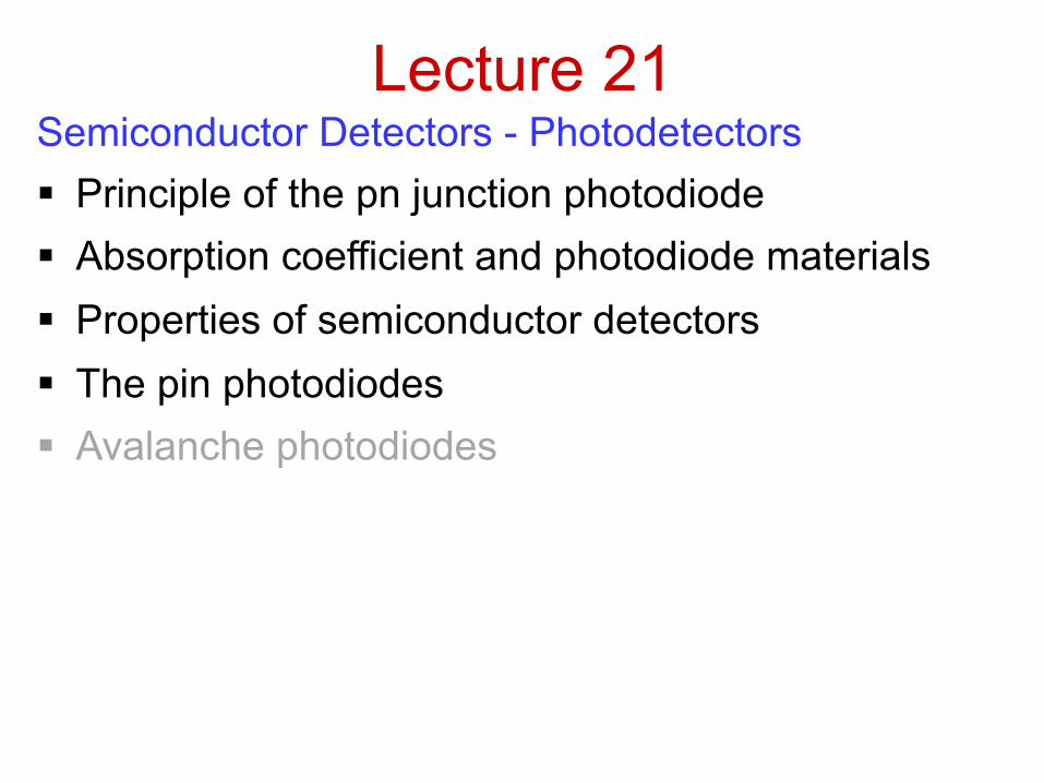
Array waveguide grating
DFB/DBR Lasers Ø High threshold Ø Non-planar Ø Integration Ø Slow Ø Expensive
Optical-electronic Conversion: Ø For switching & routing Ø Very expensive Ø Time consuming
Source 1
Source 2
Source N
Source M or Receiver M Source 1
Source 2
Source N Add/drop node
electronics fiber
Source 1
Source 2
Source N
Multiplexer D
e-M
ultip
lexe
r Multiplexer
Optical à Electrical Electrical à Optical
wire
modulators
Fiber Optic Communications
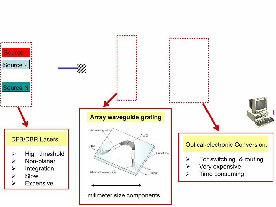
pn Junction Photodiode
§ Photons generates electron hole pairs -EHP (photogeneration)
§ Separates charged carriers (electrons and holes)
§ Annular electrode for light to enter
§ Antireflection (AR) coatings at the ends
§ Highly doped p+ region (1 micron thick)
§ Depletion zone extends to n-region (few microns)
§ Reverse biased (5-20 V) much larger than V0=1V
§ Drifting carriers cause photocurrent
Photodetector: Converts incident light to an electrical signal (voltage or current)
ndpa WNWN =
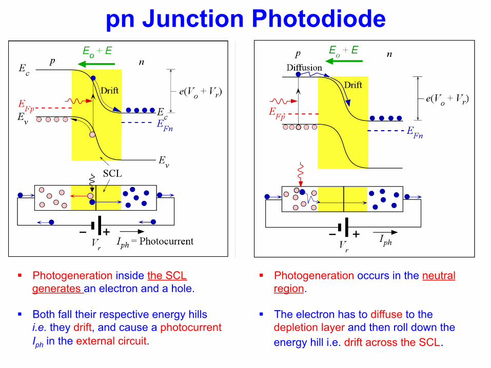
§ Photogeneration inside the SCL generates an electron and a hole.
§ Both fall their respective energy hills i.e. they drift, and cause a photocurrent Iph in the external circuit.
pn Junction Photodiode
§ Photogeneration occurs in the neutral region.
§ The electron has to diffuse to the depletion layer and then roll down the energy hill i.e. drift across the SCL.
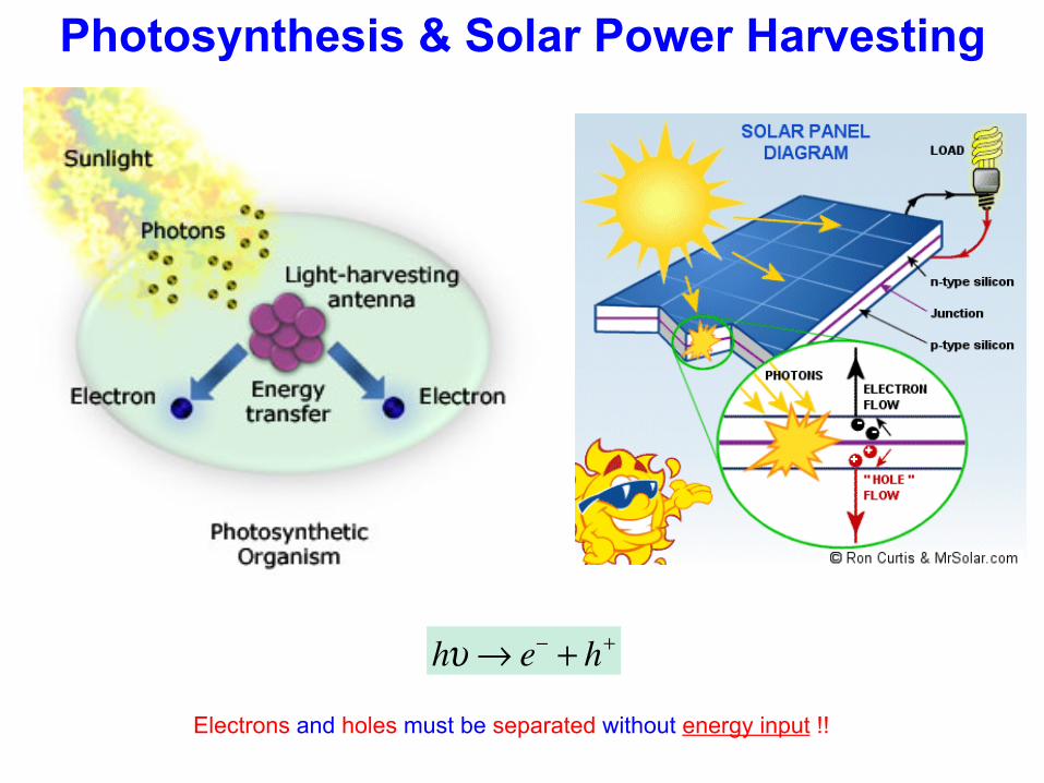
Photosynthesis & Solar Power Harvesting
Electrons and holes must be separated without energy input !!
hυ → e− + h+
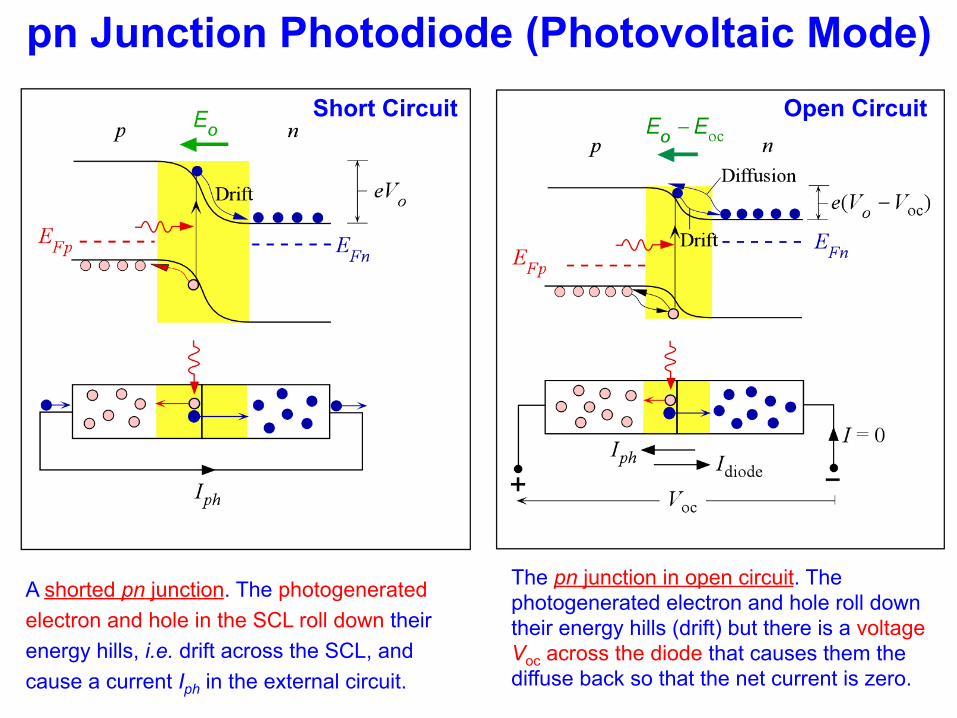
A shorted pn junction. The photogenerated electron and hole in the SCL roll down their energy hills, i.e. drift across the SCL, and cause a current Iph in the external circuit.
pn Junction Photodiode (Photovoltaic Mode) Short Circuit
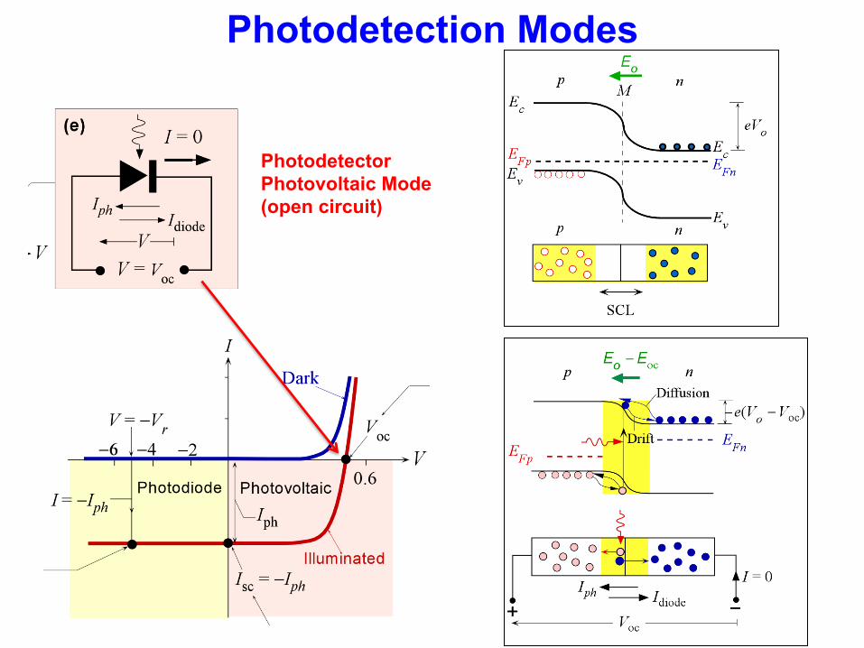
The pn junction in open circuit. The photogenerated electron and hole roll down their energy hills (drift) but there is a voltage Voc across the diode that causes them the diffuse back so that the net current is zero.
Open Circuit
Photodetection Modes
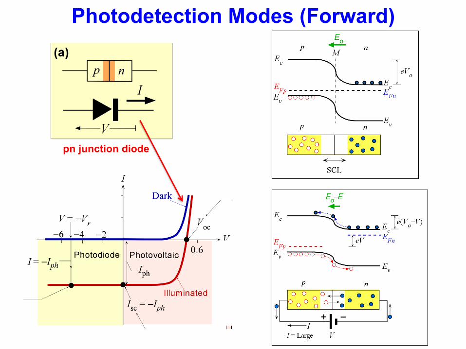
Photodetection Modes (Forward)
pn junction diode
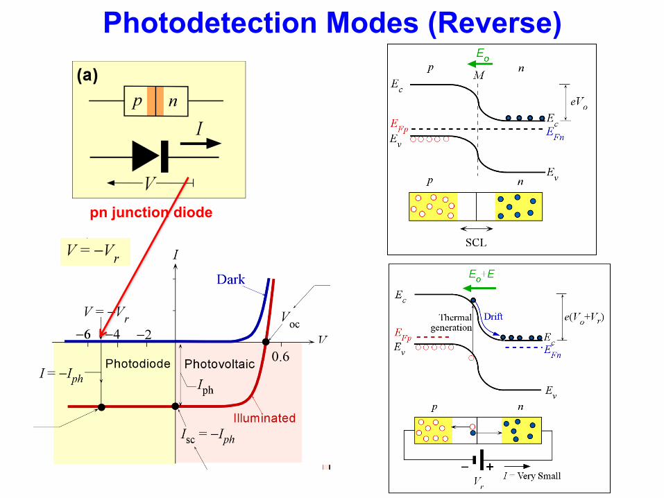
Photodetection Modes (Reverse)
pn junction diode
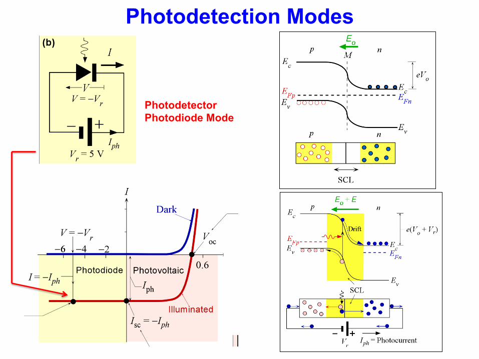
Photodetection Modes
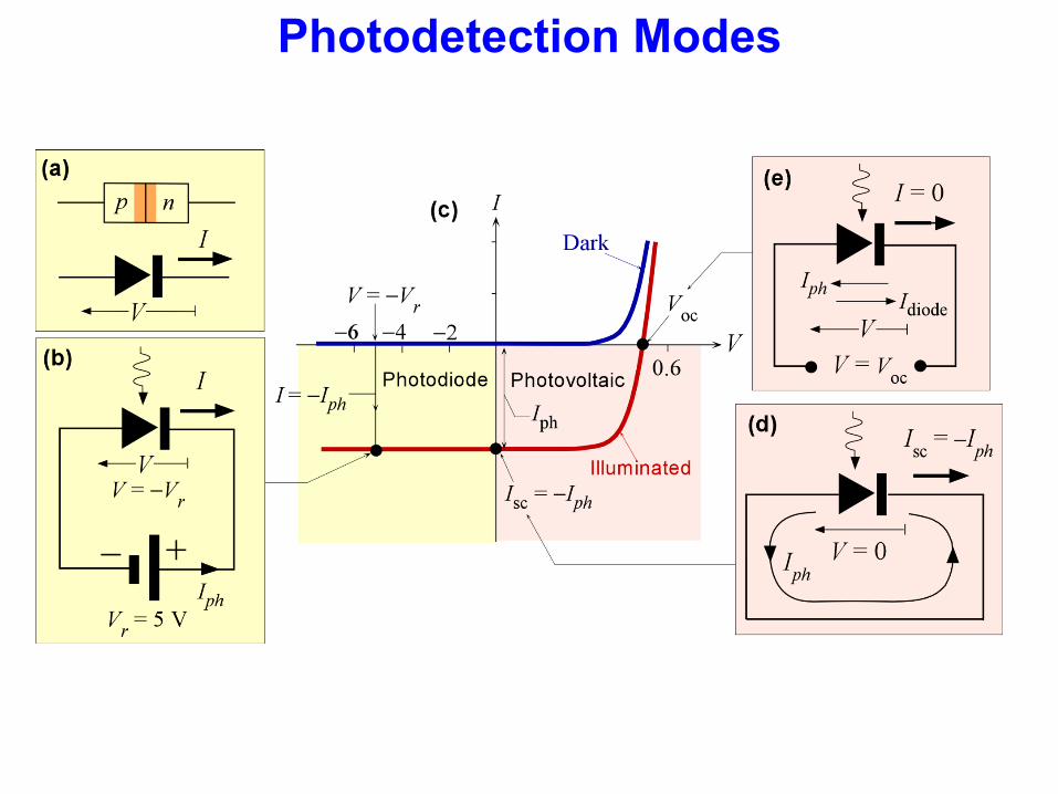
Photodetector Photodiode Mode
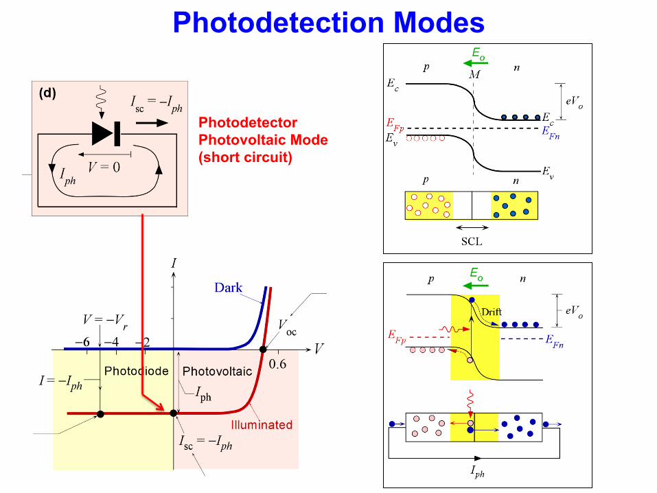
Photodetection Modes
Photodetector Photovoltaic Mode (short circuit)
Photodetection Modes
Photodetector Photovoltaic Mode (open circuit)
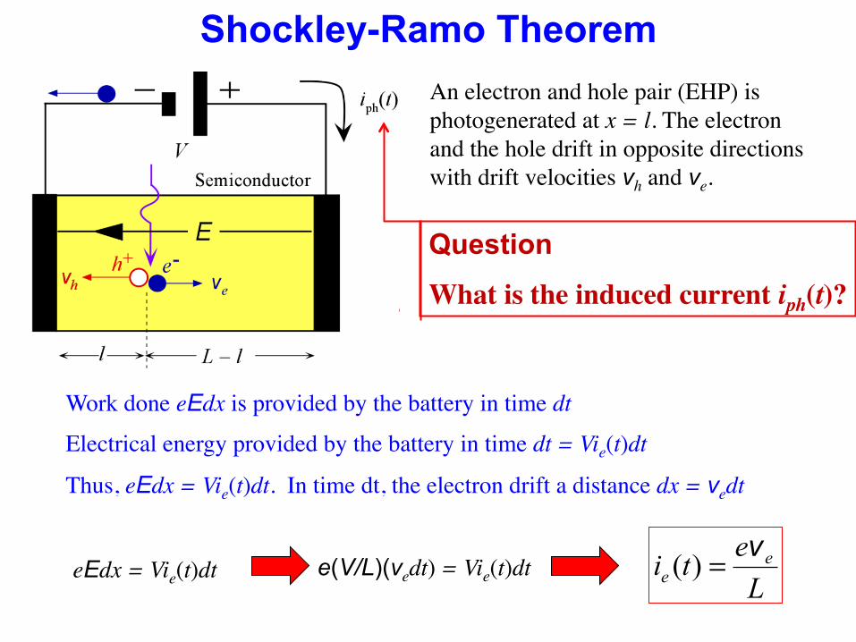
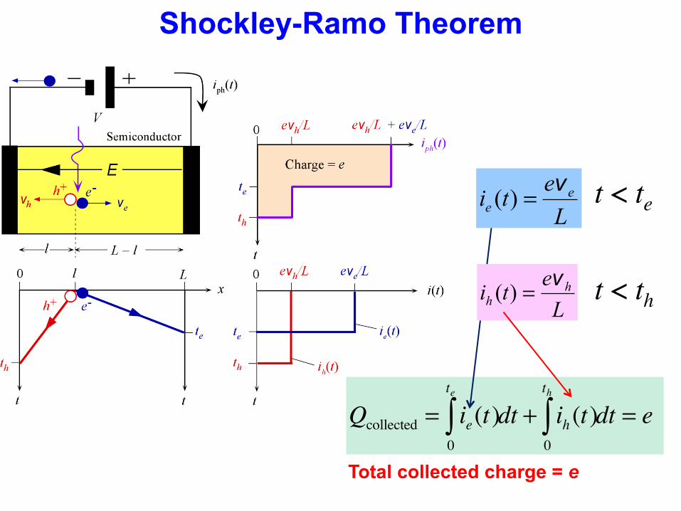
An electron and hole pair (EHP) is photogenerated at x = l. The electron and the hole drift in opposite directions with drift velocities vh and ve.
Question
What is the induced current iph(t)?
Shockley-Ramo Theorem
Work done eEdx is provided by the battery in time dt
Electrical energy provided by the battery in time dt = Vie(t)dt
Thus, eEdx = Vie(t)dt. In time dt, the electron drift a distance dx = vedt
eEdx = Vie(t)dt e(V/L)(vedt) = Vie(t)dt Leti e
ev=)(
Shockley-Ramo Theorem
ee
lLtv)( −=
th =
lvh
Electron transit times
Hole transit time
Shockley-Ramo Theorem
Qcollected = ie(t)0
te
∫ dt + ih (t)0
th
∫ dt = e
Leti e
ev=)(
Leti h
hv=)(
t < te
t < th
Total collected charge = e
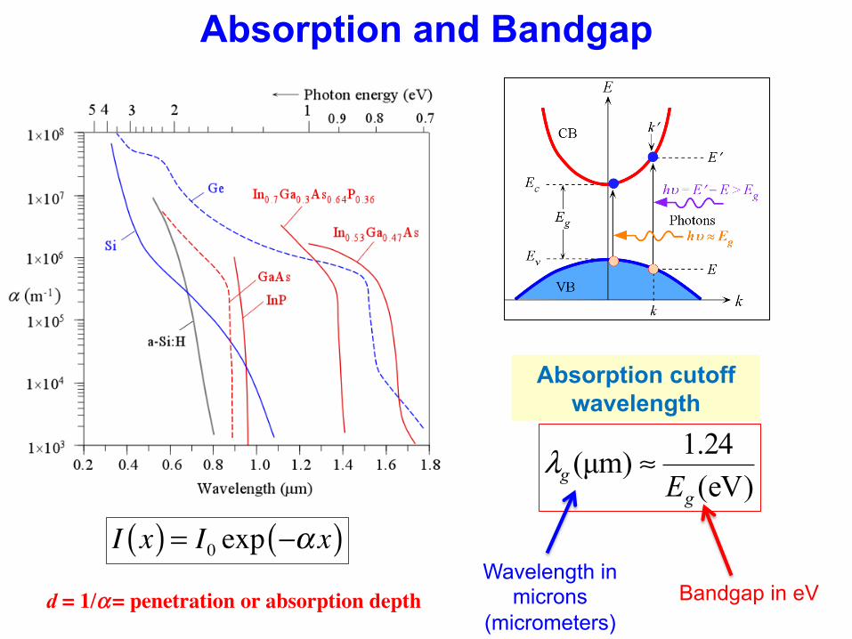
Wavelength in microns
(micrometers)
)eV(24.1)µm(
gg E
≈λ
Absorption cutoff wavelength
Bandgap in eV
Absorption and Bandgap
d = 1/α = penetration or absorption depth
I x( ) = I0 exp −α x( )
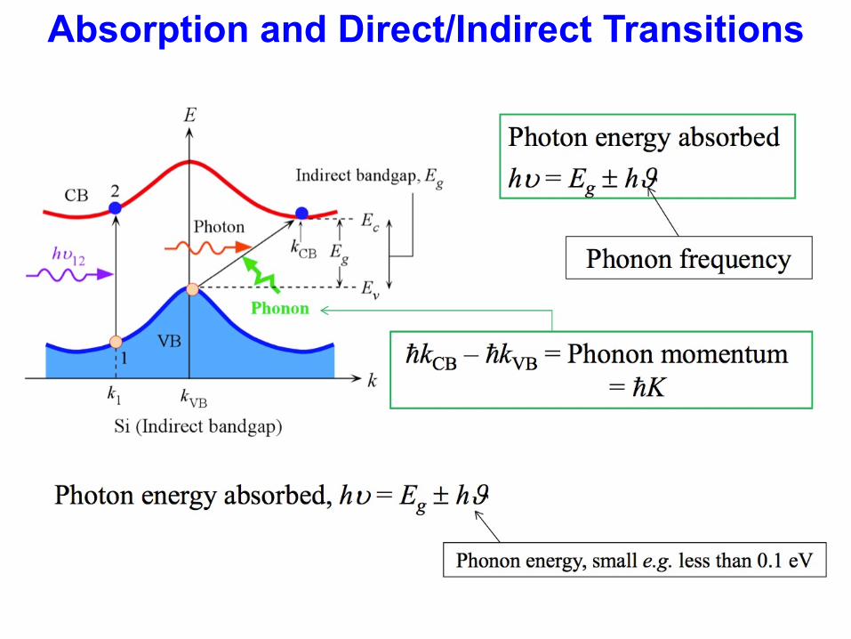
Absorption and Direct/Indirect Transitions
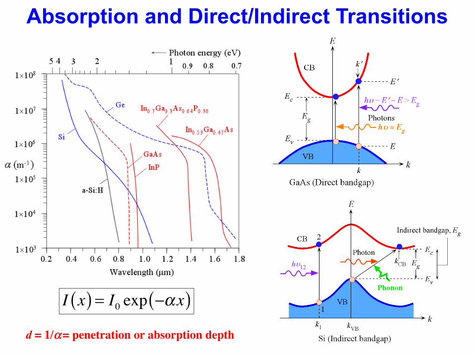
d = 1/α = penetration or absorption depth
Absorption and Direct/Indirect Transitions
I x( ) = I0 exp −α x( )
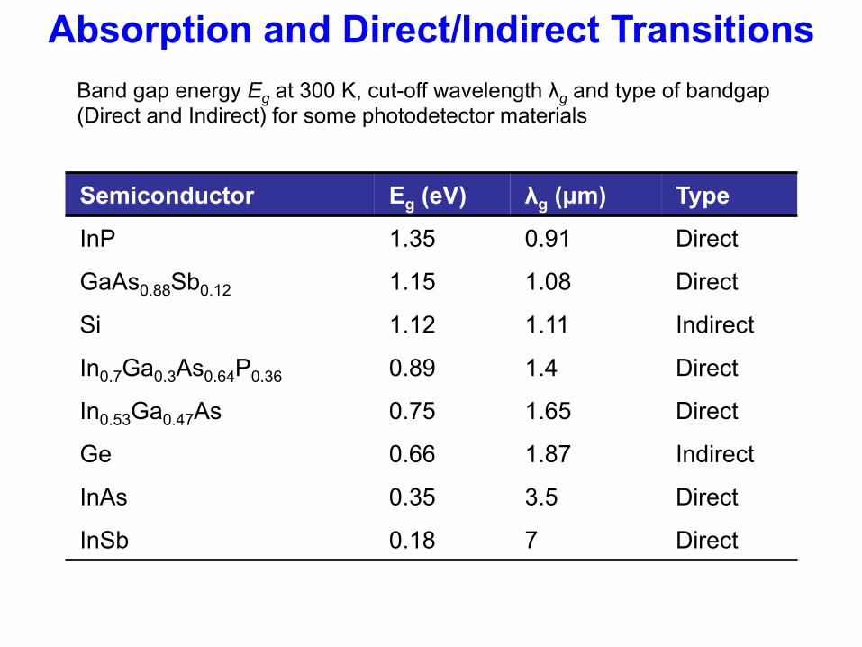
Semiconductor Eg (eV) λg (µm) Type
InP 1.35 0.91 Direct
GaAs0.88Sb0.12 1.15 1.08 Direct
Si 1.12 1.11 Indirect
In0.7Ga0.3As0.64P0.36 0.89 1.4 Direct
In0.53Ga0.47As 0.75 1.65 Direct
Ge 0.66 1.87 Indirect
InAs 0.35 3.5 Direct
InSb 0.18 7 Direct
Band gap energy Eg at 300 K, cut-off wavelength λg and type of bandgap (Direct and Indirect) for some photodetector materials
Absorption and Direct/Indirect Transitions
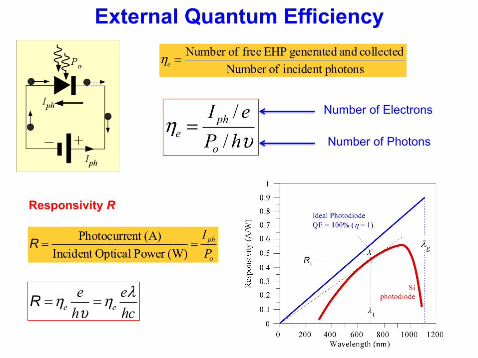
photonsincident ofNumber collected and generated EHPfree ofNumber =eη
υη
hPeI
o
phe /
/=
External Quantum Efficiency
Number of Electrons
Number of Photons
Responsivity R
o
ph
PI
==(W) Power OpticalIncident
(A)nt PhotocurreR
hce
he
eeλη
υη ==R
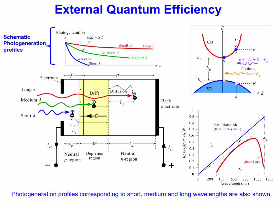
Photogeneration profiles corresponding to short, medium and long wavelengths are also shown.
Schematic Photogeneration profiles
External Quantum Efficiency
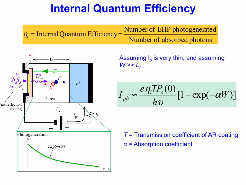
photons absorbed ofNumber atedphotogener EHPofNumber y EfficiencQuantumInternal ==iη
Assuming lp is very thin, and assuming W >> Lh
)]exp(1[)0( WhPeI oi
ph αυ
η −−≈ T
T = Transmission coefficient of AR coating α = Absorption coefficient
Internal Quantum Efficiency
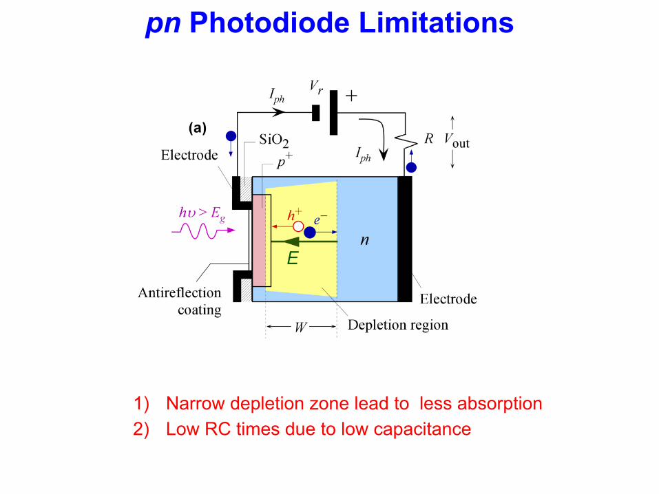
pn Photodiode Limitations
1) Narrow depletion zone lead to less absorption 2) Low RC times due to low capacitance
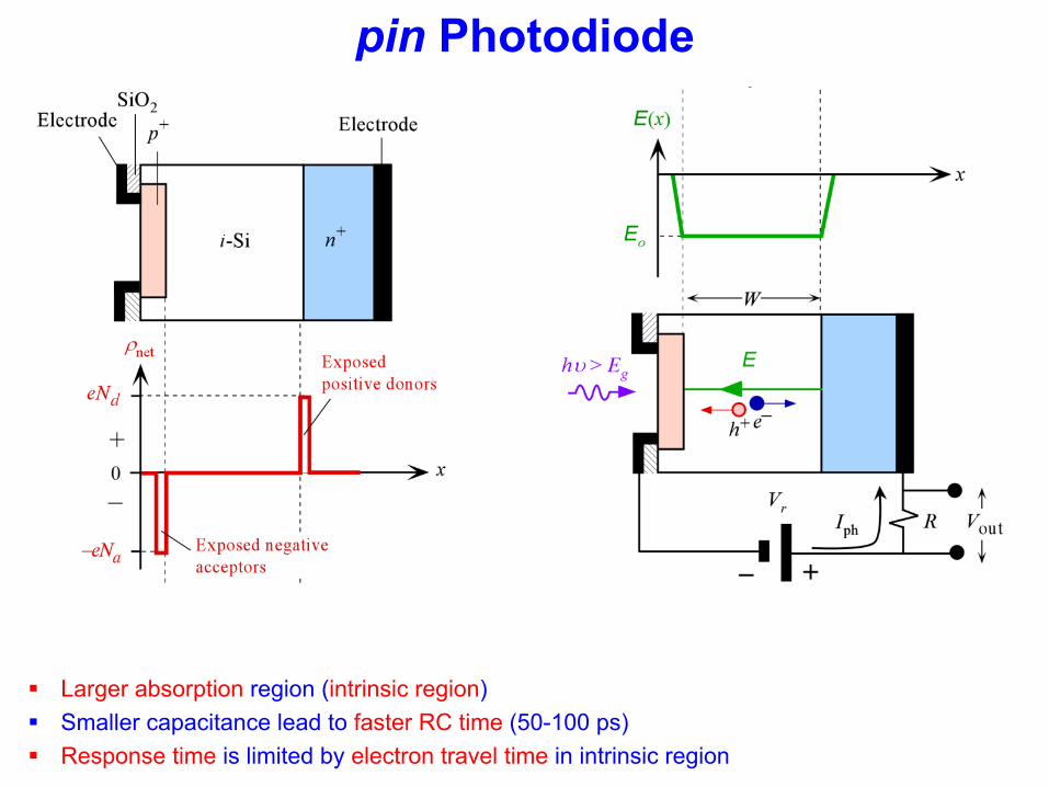
pin Photodiode
§ Larger absorption region (intrinsic region) § Smaller capacitance lead to faster RC time (50-100 ps) § Response time is limited by electron travel time in intrinsic region