Embed Size (px)
Citation preview
Semiconductor Wafer Edge Analysis/1
Semiconductor Wafer Edge Analysis
Chapman Technical Note-TW-1 waf_edge.doc Rev-98-07
Semiconductor Wafer Edge Analysis/2
Introduction
The reason for evaluating semiconductor wafer edge microroughness is that edge defects can sometimes adversely affect semiconductor performance. Problems range from features that trap liquid or airborne particles to rough surface protrusions that may become detached and release silicon particles during processing. These problems have led to an ASTM standards effort that includes the definition of a standard for the measurements of the surface topography of semiconductor edges. Chapman Instruments has participated in recent activities of both ASTM and SEMI standards committees.
This application note presents information on the types of measurements required for wafer edge processing. Edge measurements are included that show several regions at or near the actual edge boundary. These measurements include roughness parameters useful for quantifying the surface topography. Other parameters included selectively emphasize either peaks or valleys. Each of these parameters can provide distinctive information for quantifying the semiconductor edge surface conditions. Finally, guidelines are provided in accordance with the ASTM standards committee to aid in measurement of semiconductor edges.
Wafer Edge Background
Recent standard guidelines have been developed for the measurement of the edge surface roughness (ASTM edge roughness standard preliminary version only). Essentially, these guidelines define the measurement locations around the wafer edge and the reporting requirements. Two typical edge types are encountered in the semiconductor industry:
• rounded or blunt shape
• bullet or beveled shape
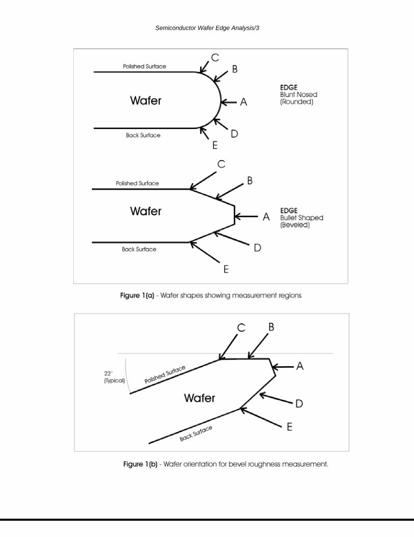
Figure 1(a) on the following page shows the two common wafer edge types and their edge geometries. Figure 1(b) shows the edge geometry shape that is specified by SEMI M1 (Semiconductor Equipment and Materials International). The bevel regions on bullet-shaped wafers are typically ground at 22-degree angles to the main surfaces of the wafer, while blunt wafers have a smooth transition from the flat wafer surface to the actual edge. Figure 1 also shows the five regions constituting the edge of the wafer. These five regions are: the transition area between the polished side and the edge (C), the front side bevel or rounded region (B), the crown or apex (A), the back side bevel or rounded region (D), and the transition area between the back side and the edge (E).
Unpolished edges typically exhibit a surface pattern formed from a grinding process. Surface peaks will touch carrier walls, while valleys will trap particles and impurities. These particles can then propagate to the wafer surface and increase the risk of wafer chipping. Also, deep wells in the edge can be a location site for phosphorus during doping. Phosphorus that is trapped in these locations can then be chipped out in handling. Thus, edge polishing may be required to minimize these surface irregularities.
Semiconductor Wafer Edge Analysis/3
Semiconductor Wafer Edge Analysis/4
Stricter requirements in the wafer manufacturing process have made edge measurements important for both 200 mm and 300 mm wafers. In fact, the SEMI standard for 300 mm wafers specifically requires a “polished edge.” Polishing the edge is done in order to reduce wafer cracking and chipping under stress during transport or thermal processing. This applies to all types of wafers, especially bonded wafers. The degree of polishing needs to be monitored by a surface inspection tool. The Chapman profiling system is capable of measuring both across and along all areas of the edge, providing the wafer manufacturer with the feedback necessary to accurately control their edge polishing process.
Wafer Edge Measurements
As outlined in the preceding paragraphs, edge roughness control is becoming an integral issue in the production of semiconductor wafers. Non-contact measurement techniques are beneficial because they do not contaminate the sample and typically do not require considerable preparation. The SEMI standards committee included the Chapman Instruments MP2000 Plus system for reporting profile and roughness information on the wafer edge. Three types of wafers were used for the SEMI standards committee study:
• caustic-etched
• acid-etched
• polished
These same three types of wafers will be used in our examples to show typical results. All measurements in this document were acquired with an MP2000 Plus Non-Contact Surface Profiler configured with a 50X objective and a Nomarski II prism. This optics combination has a spatial resolution of 0.7 µm with a maximum surface slope of 16.7 degrees.
Semiconductor Wafer Edge Analysis/5
Transition Region
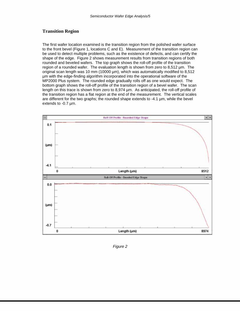
The first wafer location examined is the transition region from the polished wafer surface to the front bevel (Figure 1, locations C and E). Measurement of the transition region can be used to detect multiple problems, such as the existence of defects, and can certify the shape of the edge. Figure 2 shows measurement results from transition regions of both rounded and beveled wafers. The top graph shows the roll-off profile of the transition region of a rounded wafer. The evaluation length is shown from zero to 8,512 µm. The original scan length was 10 mm (10000 µm), which was automatically modified to 8,512 µm with the edge-finding algorithm incorporated into the operational software of the MP2000 Plus system. The rounded edge gradually rolls off as one would expect. The bottom graph shows the roll-off profile of the transition region of a bevel wafer. The scan length on this trace is shown from zero to 8,974 µm. As anticipated, the roll-off profile of the transition region has a flat region at the end of the measurement. The vertical scales are different for the two graphs; the rounded shape extends to -4.1 µm, while the bevel extends to -0.7 µm.
Figure 2
Semiconductor Wafer Edge Analysis/6
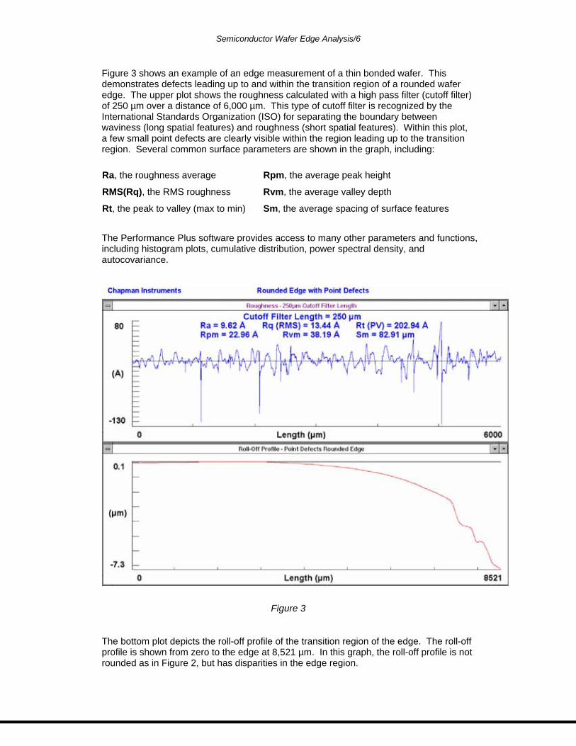
Figure 3 shows an example of an edge measurement of a thin bonded wafer. This demonstrates defects leading up to and within the transition region of a rounded wafer edge. The upper plot shows the roughness calculated with a high pass filter (cutoff filter) of 250 µm over a distance of 6,000 µm. This type of cutoff filter is recognized by the International Standards Organization (ISO) for separating the boundary between waviness (long spatial features) and roughness (short spatial features). Within this plot, a few small point defects are clearly visible within the region leading up to the transition region. Several common surface parameters are shown in the graph, including:
Ra, the roughness average Rpm, the average peak height
RMS(Rq), the RMS roughness Rvm, the average valley depth
Rt, the peak to valley (max to min) Sm, the average spacing of surface features
The Performance Plus software provides access to many other parameters and functions, including histogram plots, cumulative distribution, power spectral density, and autocovariance.
Figure 3
The bottom plot depicts the roll-off profile of the transition region of the edge. The roll-off profile is shown from zero to the edge at 8,521 µm. In this graph, the roll-off profile is not rounded as in Figure 2, but has disparities in the edge region.
Semiconductor Wafer Edge Analysis/7
Bevel
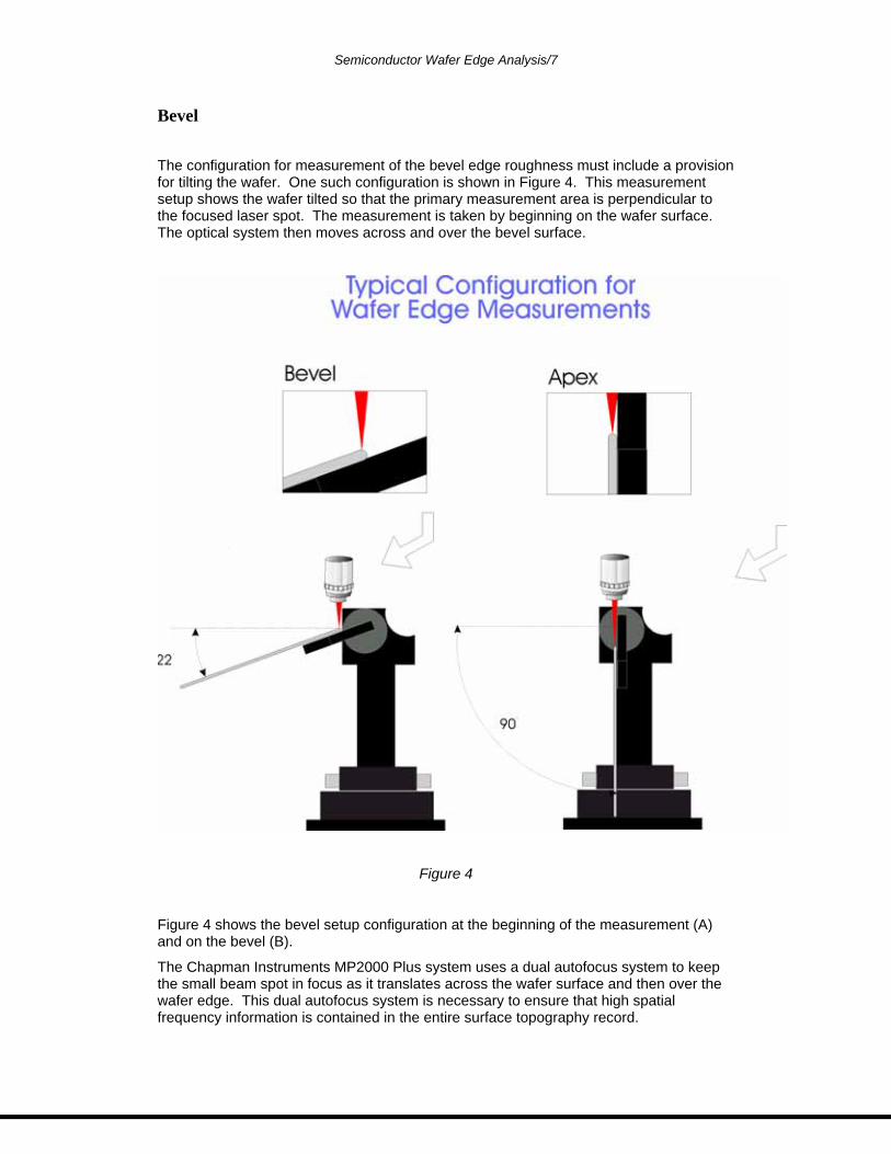
The configuration for measurement of the bevel edge roughness must include a provision for tilting the wafer. One such configuration is shown in Figure 4. This measurement setup shows the wafer tilted so that the primary measurement area is perpendicular to the focused laser spot. The measurement is taken by beginning on the wafer surface. The optical system then moves across and over the bevel surface.
Figure 4
Figure 4 shows the bevel setup configuration at the beginning of the measurement (A) and on the bevel (B).
The Chapman Instruments MP2000 Plus system uses a dual autofocus system to keep the small beam spot in focus as it translates across the wafer surface and then over the wafer edge. This dual autofocus system is necessary to ensure that high spatial frequency information is contained in the entire surface topography record.
Semiconductor Wafer Edge Analysis/8
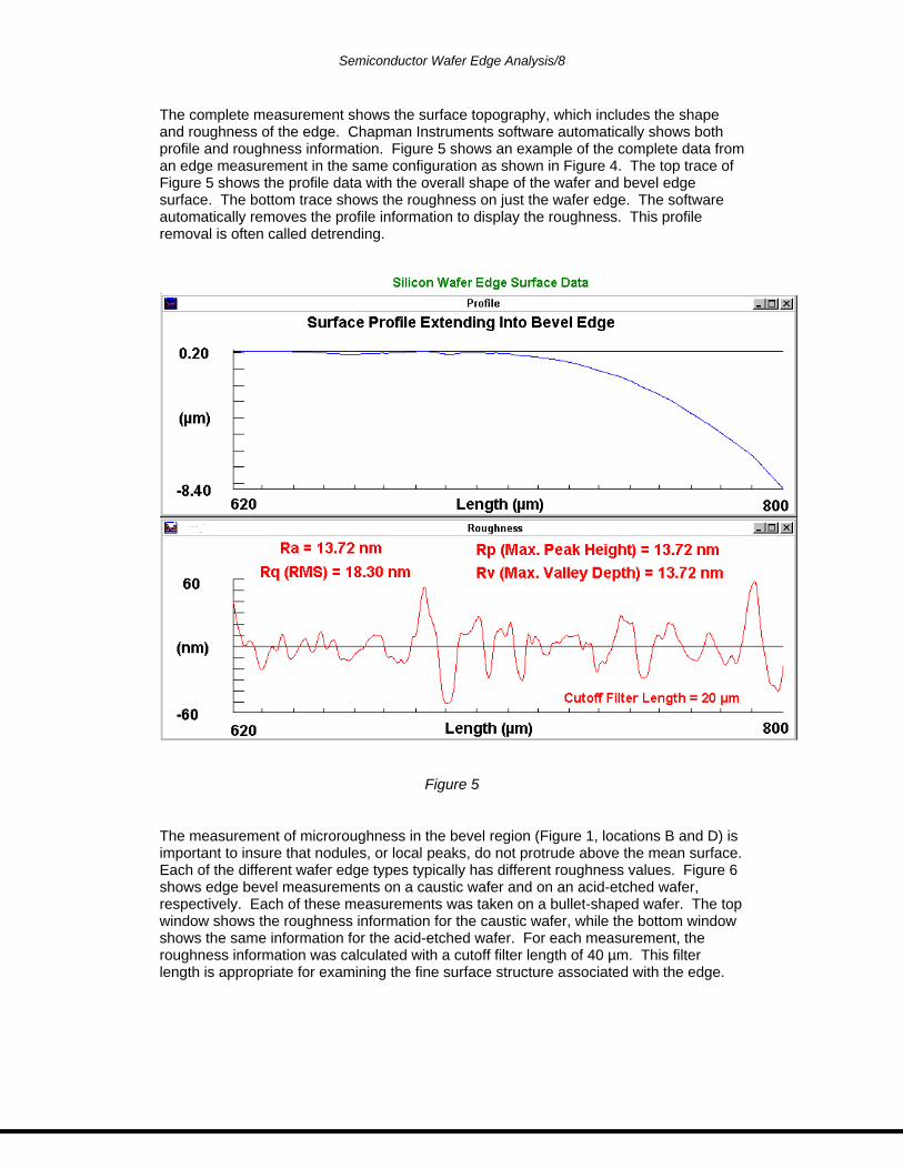
The complete measurement shows the surface topography, which includes the shape and roughness of the edge. Chapman Instruments software automatically shows both profile and roughness information. Figure 5 shows an example of the complete data from an edge measurement in the same configuration as shown in Figure 4. The top trace of Figure 5 shows the profile data with the overall shape of the wafer and bevel edge surface. The bottom trace shows the roughness on just the wafer edge. The software automatically removes the profile information to display the roughness. This profile removal is often called detrending.
Figure 5
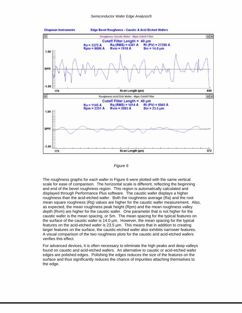
The measurement of microroughness in the bevel region (Figure 1, locations B and D) is important to insure that nodules, or local peaks, do not protrude above the mean surface. Each of the different wafer edge types typically has different roughness values. Figure 6 shows edge bevel measurements on a caustic wafer and on an acid-etched wafer, respectively. Each of these measurements was taken on a bullet-shaped wafer. The top window shows the roughness information for the caustic wafer, while the bottom window shows the same information for the acid-etched wafer. For each measurement, the roughness information was calculated with a cutoff filter length of 40 µm. This filter length is appropriate for examining the fine surface structure associated with the edge.
Semiconductor Wafer Edge Analysis/9
Figure 6
The roughness graphs for each wafer in Figure 6 were plotted with the same vertical scale for ease of comparison. The horizontal scale is different, reflecting the beginning and end of the bevel roughness region. This region is automatically calculated and displayed through Performance Plus software. The caustic wafer displays a higher roughness than the acid-etched wafer. Both the roughness average (Ra) and the root mean square roughness (Rq) values are higher for the caustic wafer measurement. Also, as expected, the mean roughness peak height (Rpm) and the mean roughness valley depth (Rvm) are higher for the caustic wafer. One parameter that is not higher for the caustic wafer is the mean spacing, or Sm. The mean spacing for the typical features on the surface of the caustic wafer is 14.0 µm. However, the mean spacing for the typical features on the acid-etched wafer is 23.5 µm. This means that in addition to creating larger features on the surface, the caustic-etched wafer also exhibits narrower features. A visual comparison of the two roughness plots for the caustic and acid-etched wafers verifies this effect.
For advanced devices, it is often necessary to eliminate the high peaks and deep valleys found on caustic and acid-etched wafers. An alternative to caustic or acid-etched wafer edges are polished edges. Polishing the edges reduces the size of the features on the surface and thus significantly reduces the chance of impurities attaching themselves to the edge.
Semiconductor Wafer Edge Analysis/10
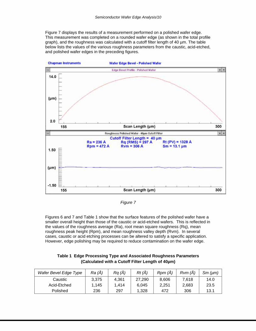
Figure 7 displays the results of a measurement performed on a polished wafer edge. This measurement was completed on a rounded wafer edge (as shown in the total profile graph), and the roughness was calculated with a cutoff filter length of 40 µm. The table below lists the values of the various roughness parameters from the caustic, acid-etched, and polished wafer edges in the preceding figures.
Figure 7
Figures 6 and 7 and Table 1 show that the surface features of the polished wafer have a smaller overall height than those of the caustic or acid-etched wafers. This is reflected in the values of the roughness average (Ra), root mean square roughness (Rq), mean roughness peak height (Rpm), and mean roughness valley depth (Rvm). In several cases, caustic or acid etching processes can be altered to satisfy a specific application. However, edge polishing may be required to reduce contamination on the wafer edge.
Table 1 Edge Processing Type and Associated Roughness Parameters (Calculated with a Cutoff Filter Length of 40µm)
Wafer Bevel Edge Type Ra (Å) Rq (Å) Rt (Å) Rpm (Å) Rvm (Å) Sm (µm)
Caustic 3,375 4,361 27,290 8,606 7,618 14.0 Acid-Etched 1,145 1,414 6,045 2,251 2,683 23.5
Polished 236 297 1,328 472 306 13.1
Semiconductor Wafer Edge Analysis/11
Crown
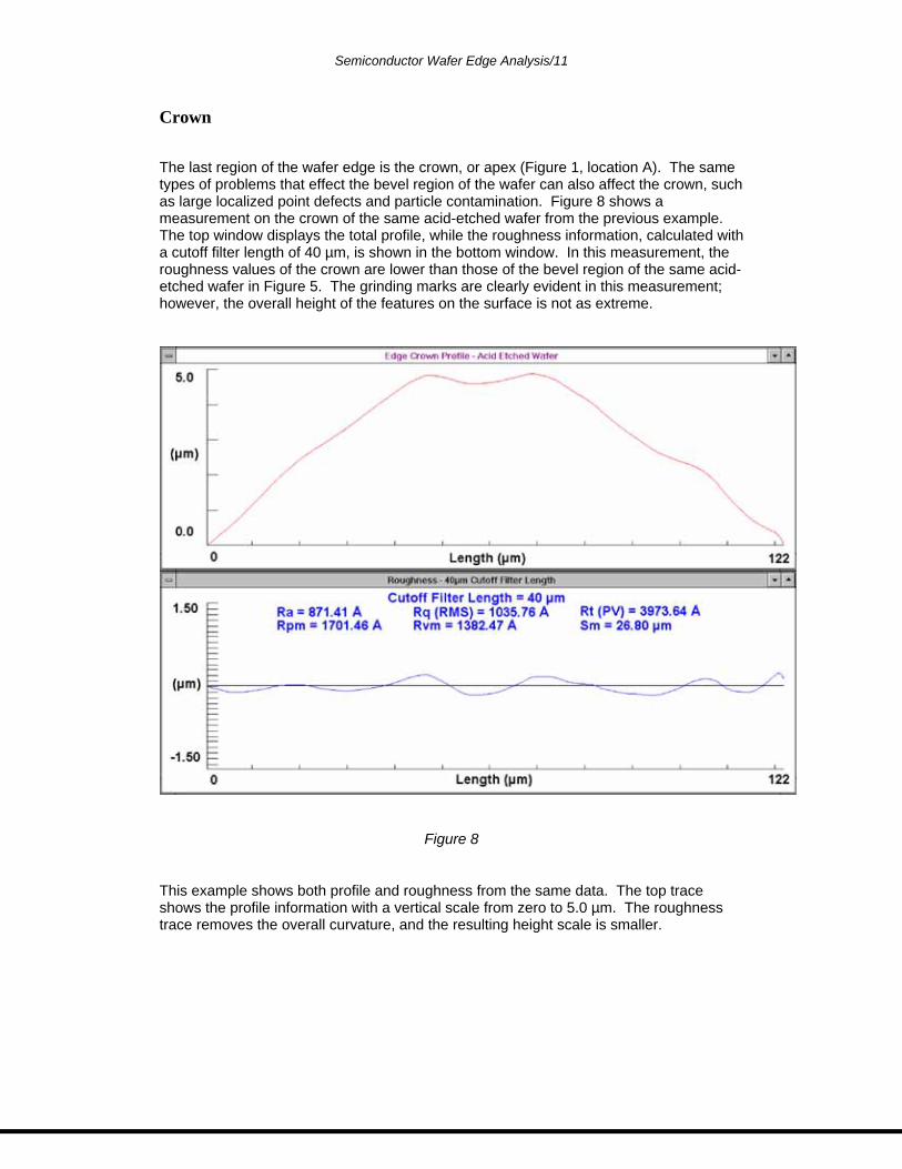
The last region of the wafer edge is the crown, or apex (Figure 1, location A). The same types of problems that effect the bevel region of the wafer can also affect the crown, such as large localized point defects and particle contamination. Figure 8 shows a measurement on the crown of the same acid-etched wafer from the previous example. The top window displays the total profile, while the roughness information, calculated with a cutoff filter length of 40 µm, is shown in the bottom window. In this measurement, the roughness values of the crown are lower than those of the bevel region of the same acid-etched wafer in Figure 5. The grinding marks are clearly evident in this measurement; however, the overall height of the features on the surface is not as extreme.
Figure 8
This example shows both profile and roughness from the same data. The top trace shows the profile information with a vertical scale from zero to 5.0 µm. The roughness trace removes the overall curvature, and the resulting height scale is smaller.
Semiconductor Wafer Edge Analysis/12
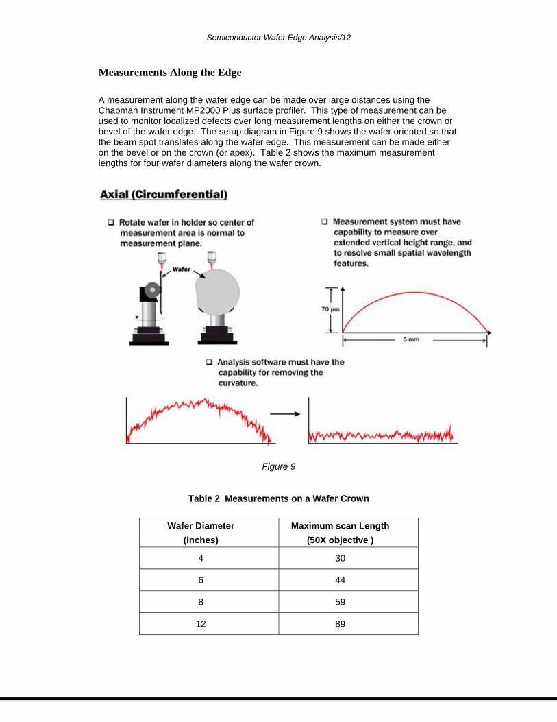
Measurements Along the Edge
A measurement along the wafer edge can be made over large distances using the Chapman Instrument MP2000 Plus surface profiler. This type of measurement can be used to monitor localized defects over long measurement lengths on either the crown or bevel of the wafer edge. The setup diagram in Figure 9 shows the wafer oriented so that the beam spot translates along the wafer edge. This measurement can be made either on the bevel or on the crown (or apex). Table 2 shows the maximum measurement lengths for four wafer diameters along the wafer crown.
Figure 9
Table 2 Measurements on a Wafer Crown
Wafer Diameter (inches)
Maximum scan Length (50X objective )
4 30
6 44
8 59
12 89
Semiconductor Wafer Edge Analysis/13
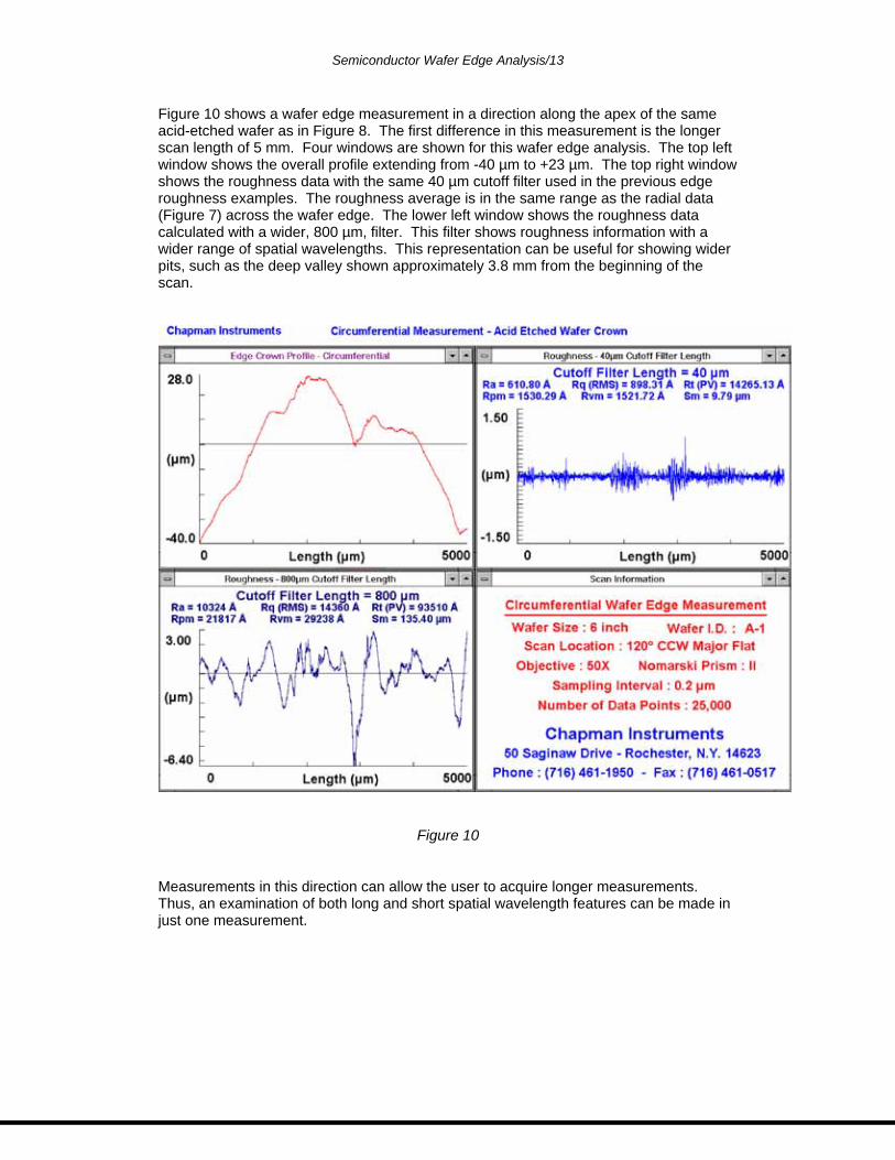
Figure 10 shows a wafer edge measurement in a direction along the apex of the same acid-etched wafer as in Figure 8. The first difference in this measurement is the longer scan length of 5 mm. Four windows are shown for this wafer edge analysis. The top left window shows the overall profile extending from -40 µm to +23 µm. The top right window shows the roughness data with the same 40 µm cutoff filter used in the previous edge roughness examples. The roughness average is in the same range as the radial data (Figure 7) across the wafer edge. The lower left window shows the roughness data calculated with a wider, 800 µm, filter. This filter shows roughness information with a wider range of spatial wavelengths. This representation can be useful for showing wider pits, such as the deep valley shown approximately 3.8 mm from the beginning of the scan.
Figure 10
Measurements in this direction can allow the user to acquire longer measurements. Thus, an examination of both long and short spatial wavelength features can be made in just one measurement.
Semiconductor Wafer Edge Analysis/14
Wafer Handling
No matter what types of measurements are performed on a silicon wafer edge, some kind of wafer fixture is necessary for handling and positioning the wafer. Chapman Instruments offers three types of wafer positioners:
• a manually adjustable multi-axis edge fixture
• a motorized multi-axis wafer positioner
• a 3-D (area) measurement positioner
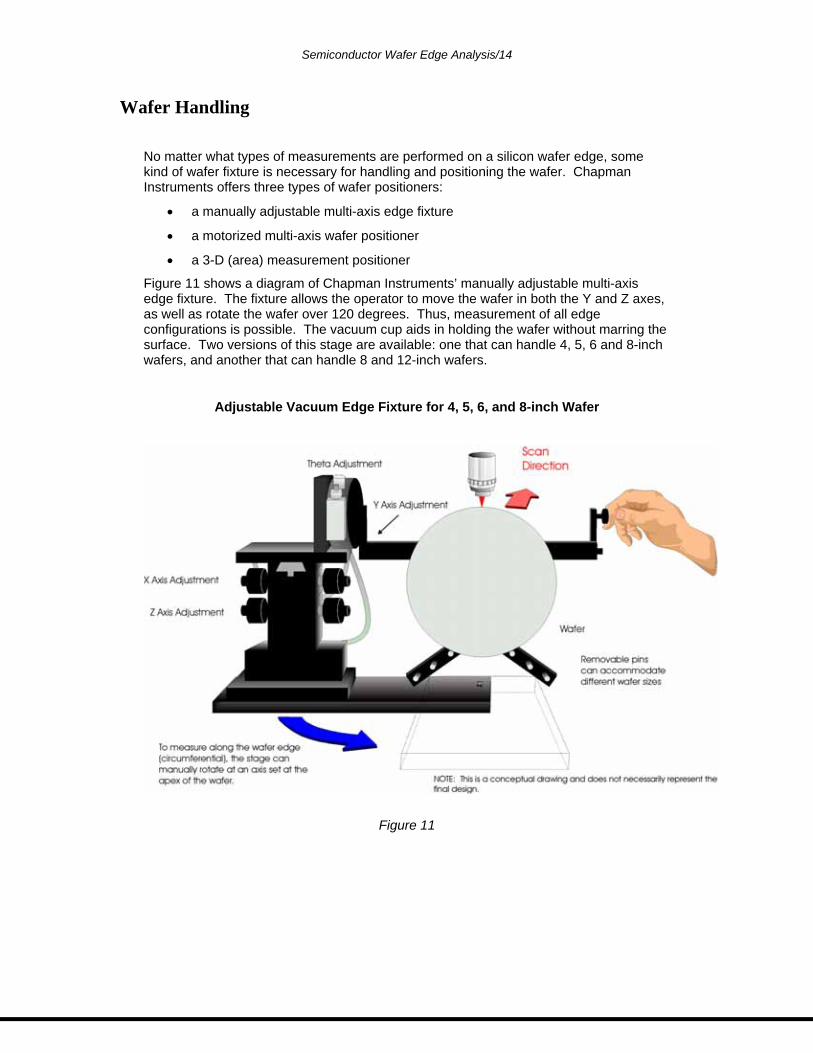
Figure 11 shows a diagram of Chapman Instruments’ manually adjustable multi-axis edge fixture. The fixture allows the operator to move the wafer in both the Y and Z axes, as well as rotate the wafer over 120 degrees. Thus, measurement of all edge configurations is possible. The vacuum cup aids in holding the wafer without marring the surface. Two versions of this stage are available: one that can handle 4, 5, 6 and 8-inch wafers, and another that can handle 8 and 12-inch wafers.
Adjustable Vacuum Edge Fixture for 4, 5, 6, and 8-inch Wafer
Figure 11
Semiconductor Wafer Edge Analysis/15
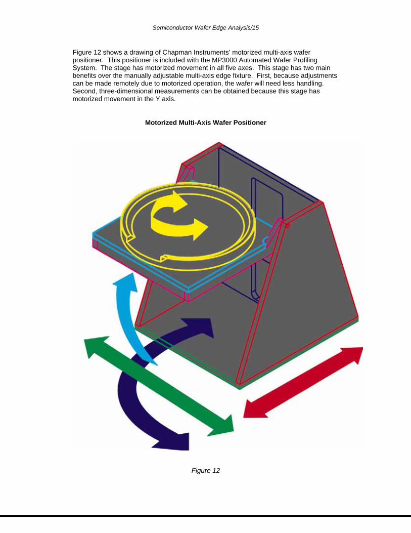
Figure 12 shows a drawing of Chapman Instruments’ motorized multi-axis wafer positioner. This positioner is included with the MP3000 Automated Wafer Profiling System. The stage has motorized movement in all five axes. This stage has two main benefits over the manually adjustable multi-axis edge fixture. First, because adjustments can be made remotely due to motorized operation, the wafer will need less handling. Second, three-dimensional measurements can be obtained because this stage has motorized movement in the Y axis.
Motorized Multi-Axis Wafer Positioner
Figure 12
Semiconductor Wafer Edge Analysis/16
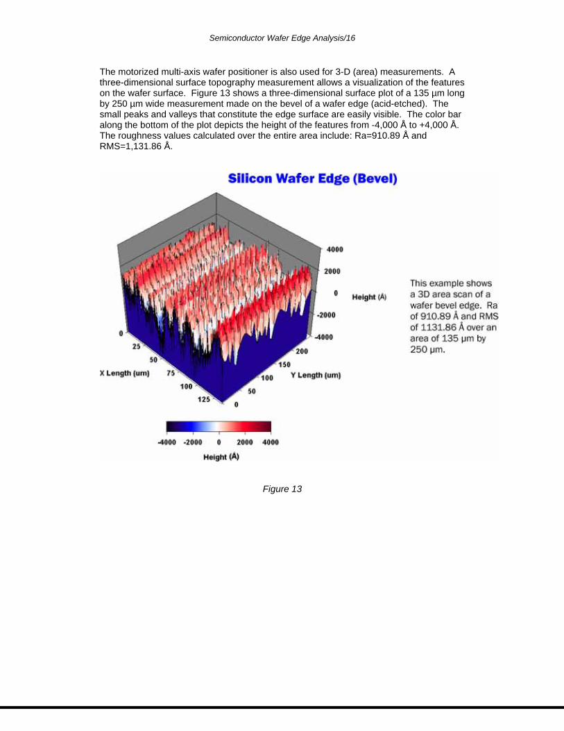
The motorized multi-axis wafer positioner is also used for 3-D (area) measurements. A three-dimensional surface topography measurement allows a visualization of the features on the wafer surface. Figure 13 shows a three-dimensional surface plot of a 135 µm long by 250 µm wide measurement made on the bevel of a wafer edge (acid-etched). The small peaks and valleys that constitute the edge surface are easily visible. The color bar along the bottom of the plot depicts the height of the features from -4,000 Å to +4,000 Å. The roughness values calculated over the entire area include: Ra=910.89 Å and RMS=1,131.86 Å.
Figure 13
Semiconductor Wafer Edge Analysis/17
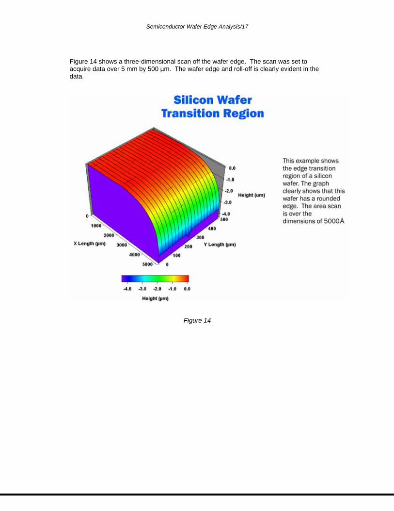
Figure 14 shows a three-dimensional scan off the wafer edge. The scan was set to acquire data over 5 mm by 500 µm. The wafer edge and roll-off is clearly evident in the data.
Figure 14
Semiconductor Wafer Edge Analysis/18
Measurement Guidelines
Utilizing the SEMI Standards Committee study and these examples, the following guidelines for the measurement of semiconductor wafers can be used:
• Semiconductor wafers should be measured utilizing a non-destructive means to avoid further contamination.
• The measurement tool should have the ability to measure sub-micrometer features on the wafer edge.
• Measurements can be performed at several locations on the wafer edge: front transition region, front bevel, apex, back bevel, and back transition region.
• For the measurement of caustic and acid-etched wafers, the measurements should be at least in a radial direction (across the grinding lines), while for polished edges, measurements can be executed both radially and circumferentially.
• Measurements should be performed on the wafers at the following locations: 15°, 165°, 195°, and 270° (Primary Fiducial). These locations are representative of the edge exhibiting the greatest magnitude of roughness, but not subject to interference from unrelated edge anomalies (i.e. orientation dependency, secondary fiducials, etc.).
• Measurement results should be reported with at least the roughness average (Ra) and the root mean square roughness (Rq) for each location, along with the appropriate cutoff filter. Additional specific parameters, such as Rpm, Rvm, and Sm, should be used whenever possible.
Conclusions
Edge measurements are becoming more critical in the manufacture of semiconductor wafers due to tighter specifications in defect and contamination control, especially for 300 mm wafers. Wafer manufacturers should follow the guidelines specified by SEMI and ASTM when monitoring their processes.
As the enclosed examples show, Chapman profilers are able to make non-destructive measurements of the wafer edges with sub-micrometer spatial resolution. With the many staging and handling options, wafers can be loaded and moved to a wide range of positions, and features can be visually inspected and accurately located with the inline Nomarski viewing system.
For more information on how the MP2000 Plus and MP3000 profiling systems can be used to measure wafer edges, contact Chapman Instruments.
3 Townline Circle Rochester, NY 14623 Phone: 585-424-1380
Fax: 585-424-2142 E-Mail: [email protected]