Embed Size (px)
Citation preview


• Editorial-Chief
Kiyoshi Sakai • Editorial Advisors
Toshio Masujima Maki Ikegami Makoto Egashira Koji Miyahara Chikao Nishida Hideaki Okada Yoshiki Hama Tetsuyuki Yanase Takefumi Tsukada Tatsuya Ichihashi Masato Nagasawa Daisuke Kawai Masato Oshita Toshihiro Kurita
• Vol. 143 Feature Articles Editor
Yoshikatsu Nagashima • Editorial Inquiries
Hirotoshi Yonezawa Corporate Total Productivity Management & Environmental Programs Fax +81-3-3218-2465
• Product Inquiries
America Tony Sibik Powerex, Inc. 173 Pavilion Lane Youngwood, PA 15697-1800, USA Marketing Fax: +1-724-925-4393 Web: www.pwrx.com Europe Robert Wiatr Mitsubishi Electric Europe,B.V. German Branch Gothaer Strasse 8, 40880 Ratingen, Germany Power device marketing Fax: +49-2102-486-3670 China Qian Yu Feng Mitsubishi Electric & Electronics (Shanghai) Co.,Ltd. 29F, Shanghai Maxdo Centre No.8, XingYi Road, ChangNing, Shanghai, P.R.C. Marketing Fax: +86-21-5208-1502 Mitsubishi Electric Advance is published on line quarterly (in March, June, September, and December) by Mitsubishi Electric Corporation. Copyright © 2013 by Mitsubishi Electric Corporation; all rights reserved. Printed in Japan.
The company names and product names described herein are the trademarks or registered trademarks of the respective companies.
CONTENTS
Technical Reports
Overview ..........................................................................................1 by Gourab Majumdar Development of SiC Power Devices – Present Status ................2 by Naoki Yutani and Hiroshi Watanabe 1.7kV Hybrid SiC Power Module with Large Current Capacity and Low Power Loss ......................................................................5 by Shigeru Hasegawa and Kazuhiro Morishita 1,200 V HVIC Technology for Power Inverter System .................9 by Manabu Yoshino and Kazuhiro Shimizu 1200V/50A Large DIPIPM Ver. 4 ...................................................12 by Tomofumi Tanaka and Takuya Shiraishi The IGBT Module for Three-Level Bidirectional Switch Type Inverter ...........................................................................................15 by Satoshi Kawabata, Hiroki Muraoka and Ayumi Maruta “J-Series” IPM and T-PM for EV and HEV Applications ............17 by Seiichiro Inokuchi and Mikio Ishihara
MITSUBISHI ELECTRIC
Sep. 2013 / Vol. 143
Precis
Mitsubishi Electric offers a wide variety of power electronics products to satisfy various customer needs, ranging from home appliances to industrial, automotive and railway application products. In addition, developments of new SiC devices are now intensively underway.
Power Device

*Fellow, Semiconductor & Device Group Mitsubishi Electric ADVANCE September 2013 1
TECHNICAL REPORTS
Overview
Author: Gourab Majumdar*
Power Devices – Key to Energy Conservation
With the rapid increase in world population and economic growth in developing nations, the demand for energy has been steadily increasing. Among energy resources, fossil fuels still pose various problems including dwindling reserves, unstable supply, and risk of price increase, and thus attention is increasingly focused on renewable sources such as wind and solar power as “new energies.” Meanwhile, the efficient use of energy is becoming more important. Since electric power is the most convenient and widely used form for the supply and use of these energies, technological development of power electronics is indispensable for the efficient use of power energy.
Mitsubishi Electric serves the market by supplying not only power electronics equipment but also power devices, the key components for such equipment. Silicon materials have usually been used for power devices, and their evolution has helped to reduce power losses and downsize equipment. Mitsubishi Electric has pioneered in developing and introducing advanced power device technologies, including various generations of insulated gate bipolar transistor (IGBT) modules and intelligent power modules (IPM), continuously. In addition, Mitsubishi Electric has moved forward in developing post-silicon silicon carbide (SiC) power devices, which have great potential for dramatically changing the world of power electronics in the near future. This issue introduces the latest technology trends in such areas of Mitsubishi Electric’s power devices.

*Power Device Works **Advanced Technology R&D Center 2
TECHNICAL REPORTS
Development of SiC Power Devices − Present Status
Authors: Naoki Yutani* and Hiroshi Watanabe**
1. Introduction
This paper reports the development of a silicon carbide (SiC) metal oxide semiconductor field effect transistor (MOSFET) having a withstand voltage of 1,200 V with an integrated current sensor for over-current protection, as well as the development of a SiC Schottky barrier diode (SBD) having a withstand voltage of 3.3 kV.
2. Background
Attention is now focused on SiC power devices, which are the key to achieving low power loss and compact size for next-generation power electronics equipment. SiC is a new semiconductor material that has higher breakdown strength than silicon (Si), and thus enables the fabrication of low-resistance, high-voltage devices. In addition, SiC allows the design of unipolar devices such as MOSFETs and SBDs, which provide lower switching loss than bipolar Si devices.
At present, commercially available SiC power de-vices include SBDs having a withstand voltage in the range of 600 to 1,200 V, and transistors such as MOS-FETs are also available from multiple manufacturers. To date, Mitsubishi Electric has developed a 1,200 V MOSFET and SBD, and a prototype SiC inverter with a power output of 11 kW, which demonstrated a 70% loss reduction from the level of conventional inverters. Mit-subishi Electric has also developed a 1.7 kV SiC SBD, which was integrated with an Si-insulated gate bipolar transistor (Si-IGBT) into a 1.7 kV/1,200 A high-voltage, high-capacity inverter module.
For industrial and railway vehicle applications, SiC power devices must achieve not only a low power loss, but also high functionality, high withstand voltage and large current capacity. For practical applications of the intelligent power module (IPM) with integrated current sensor for over-current protection, the SiC power de-vice needs to have a current sensing function. In addi-tion, a 3.3kV class high withstand voltage is strongly desired for SiC power devices.
This paper describes the development of the 1,200 V SiC-MOSFET with an integrated current sensor, as well as the design of a termination structure for the 3.3kV class withstand voltage, and the SiC-SBD using this termination structure.
3. SiC-MOSFET with Built-In Current Sens-ing Function
Mitsubishi Electric has developed the world’s first SiC-MOSFET with an integrated current sensor. For the current sensing function, a sense current is separated from the main current flowing through the MOSFET, which is then monitored by the protection circuit in the IPM’s control board. Upon detection of an over-current due to a short circuit, the drive circuit is shut off to avoid breakage of the element and to protect the equipment in which the IPM is installed. For low-resistance SiC power devices, especially, this shut-off protection needs to operate at a high speed. Figure 1 shows a chip photo of the SiC-MOSFET with an integrated current sensor and its equivalent circuit, which depicts the over-current detection scheme using a shunt resistor. The main cell, which is arranged in the source electrode region, con-sists of multiple MOSFET unit cells each 10 μm in size and connected in parallel. The sense cell connected to the sense electrode has the same structure as the main cell but with fewer cells connected in parallel. The main cell and the sense cell are both connected to the com-mon drain and gate electrodes, while the main cell is connected to the source electrode and the sense cell is connected to the sense electrode. Part of the drain cur-rent is separated as the sense current, which passes through the sense cell and then flows into the shunt resistor connected to the sense electrode. When the voltage across the shunt resistor rises as the sense current increases, the shunt resistance and the reference voltage are adjusted so that a shut-off signal is generated if an excessive main current flows in the circuit.
Source electrode
SiC-MOSFETs
Gate SenseGate
+-
Sense Source
Drain
Sense current
Resistor
Vref
Main current
Fig. 1 SiC-MOSFET with integrated current sensor

Mitsubishi Electric ADVANCE September 2013 3
TECHNICAL REPORTS
Figure 2 shows the main current versus drain-source voltage (VDS) and the sense current versus VDS characteristics at room temperature of the SiC-MOSFET with integrated current sensor. A specific ON resistance of 3.7 mΩcm2 is obtained at a gate voltage of 15 V. In Fig. 2, while the absolute values of the main and sense currents are different due to the difference in the number of unit cells, their VDS de-pendence shows a similar shape. In addition, although not shown in the figure, an avalanche breakdown volt-age during the gate OFF period of over 1,400 V has been achieved.
VGS =15V 10V
5V
0
25
50
75
100
0 1 2 3 4 5 6
Imai
n (
A)
VDS (V)
0
5
10
15
20
0 1 2 3 4 5 6
Isen
se (
mA
)
VDS (V)
VGS =15V 10V
5V
VGS =15V 10V
5V
0
25
50
75
100
0 1 2 3 4 5 6
Imai
n (
A)
VDS (V)
0
5
10
15
20
0 1 2 3 4 5 6
Isen
se (
mA
)
VDS (V)
VGS =15V 10V
5V
Fig. 2 Imain-VDS, Isense-VDS characteristics
The current sense ratio (ratio of the main current to
the sense current) stayed at an almost constant value of 4,400 for the main current up to 90 A at 25°C. The current sense ratio showed only small temperature dependence, with a decrease of 10% or less from 25°C to 175°C.
Figure 3 depicts the over-current detection and dynamic shut-off characteristics at 25°C for the SiC-MOSFET with integrated current sensor. As shown in Fig. 3, as the main current (Imain) increases, the sense voltage (Vsense) rises; once the sense voltage reaches the shut-off level, the gate voltage (Vgs) is turned off by the protection circuit and the main current is shut off as normal. The same performance was also achieved at 175°C.
Over-current detection
Time(ms)
Vds
(V)
Vg
s(V
)
I mai
n(A
)V
sens
e(V
)
Fig. 3 Dynamic shut-off waveforms
4. 3.3 kV SiC-SBD The breakdown electric field strength of SiC is
about 10 times higher than that of Si. Because of this higher breakdown strength, the drift layer that deter-mines the withstand voltage can be fabricated to have a higher doping concentration and a smaller thickness, and thus the resistance of SiC devices can be made lower than that of Si devices. However, the field strength also increases in the termination structure on the periphery of the element compared with the Si devices, and thus it becomes critical to design a termi-nation structure that reduces the field strength and ensures the withstand voltage. Consequently, we ex-amined the termination structure for the 3.3 kV SiC-SBD by using a device simulator, and designed a pseudo-multi-level reduced surface field (RESURF) structure, as illustrated in Fig. 4. A ring-shaped region around the edge of the Schottky electrode is ion-implanted with p-type impurities (Al) to form a guard ring. However, if the guard ring is formed as a simple ring, the field strength in the outer region of the ring rises too high locally to ensure a withstand voltage in the range of 3.3 kV. The termination structure for the 3.3 kV operations needs to be designed so that the voltage gradually decreases outward in the termination region to avoid such local high field strength. To fabri-cate the pseudo-multi-level RESURF structure shown in Fig. 4, the high- and low-dose Al ion implantation proc-esses are performed using two implantation masks. In Fig. 4, region is ion-implanted for both the high- and low-dose processes, for high-dose only, and for low-dose only. In regions , and , the effective doping concentration is controlled by varying the com-bination of high- and low-dose processes. As a result, six zones with different effective doping concentrations are formed in regions through . In this manner, the RESURF structure enables the field strength to be reduced by controlling the distribution of impurity con-centration stepwise in the termination region.
Fig. 4 Pseudo-multi-level RESURF structure In the termination region, the concentration of
ion-implanted impurities was optimized by using the device simulator. As a result, with respect to the break-down electric field strength of SiC, 3 MV/cm, a suffi-ciently low field strength of 2 MV/cm has been achieved even at the edge of the Ti electrode of SBD and 2.3
Anode Edge termination Schottky metal (Ti)
Drift region
Substrate
Cathode

4
TECHNICAL REPORTS
MV/cm in the area where the doping concentration changes significantly.
By applying the pseudo-multi-level RESURF structure optimized by using the breakdown voltage simulation, a prototype 3.3 kV SiC-SBD was fabricated. The SBD device was formed on a 30 μm thick SiC epitaxial film with doping concentration of 3 × 10¹⁵/cm−3 grown on n-type 4H-SiC substrate. After the pseudo-multi-level RESURF structure was formed by Al ion implantation, a Ti Schottky barrier was formed, and then Al and Ni electrodes were formed on the front and rear surfaces, respectively.
Figure 5 shows the reverse current-voltage charac-teristics of the prototype SiC-SBD at 25°C and 150°C. The graph plots the leakage current density versus ap-plied voltage. As shown by the graph, a breakdown current occurs at nearly the same voltage of 3.9 kV at both 25°C and 150°C. When 3.3 kV was applied, the reverse leakage current density was 2.4 × 10⁻⁴ A/cm2 (25°C), which was within the range expected as a re-verse current of the SBD, and no abnormal leakage current was observed. Figure 6 shows the forward cur-rent-voltage characteristics of the SiC-SBD at various temperatures (25°C, 100°C and 150°C). The forward voltage at a current density of 150 A/cm2 was 1.9 V at 25°C and 3.5 V at 150°C, which was expected from the impurity concentration and thickness of the drift layer.
0.00
0.02
0.04
0.06
0.08
0.10
0 1,000 2,000 3,000 4,000 5,000
25
150
Reverse voltage (V)
Lea
kage
cu
rre
nt d
ensi
ty (
A/c
m2 )
25°C150°C
3,900V
0.00
0.02
0.04
0.06
0.08
0.10
0 1,000 2,000 3,000 4,000 5,000
25
150
Reverse voltage (V)
Lea
kage
cu
rre
nt d
ensi
ty (
A/c
m2 )
25°C150°C
3,900V
Fig. 5 Reverse characteristics of 3.3 kV SiC-SBD
Fig. 6 Forward characteristics of 3.3kV SiC-SBD
As described above, the SiC-SBD was fabricated by applying the pseudo-multi-level RESURF design to the termination structure, and demonstrated sufficiently high withstand voltage performance for the 3.3 kV device.
We will further optimize the termination structure developed in this project for application to MOSFET devices, as well as develop higher-capacity devices.
Part of this research project is the outcome of the “Novel Semiconductor Power Electronics Project Real-izing Low Carbon Emission Society” commissioned by the Ministry of Economy, Trade and Industry and NEDO.
0
50
100
150
200
0 1 2 3 4 5
25°C
100°C
150°C
Forward voltage (V)
Cur
rent
den
sity
(A/c
m2 )
0
50
100
150
200
0 1 2 3 4 5
25°C
100°C
150°C
Forward voltage (V)
Cur
rent
den
sity
(A/c
m2 )

*Power Device Works Mitsubishi Electric ADVANCE September 2013 5
TECHNICAL REPORTS
1.7kV Hybrid SiC Power Module with Large Current Capacity and
Low Power Loss Authors: Shigeru Hasegawa* and Kazuhiro Morishita*
1. Introduction
Silicon (Si) power modules have been widely used for industrial inverters, such as in the railway and elec-tric power fields. Recently, for more efficient use of energy, there is a growing need for reduced power loss, smaller size and higher performance, and so attention is focusing on silicon carbide (SiC) as a new semicon-ductor material, which can reduce power loss and operate at high temperature.
Mitsubishi Electric has commercialized a 1.7 kV hybrid SiC power module integrating SiC schottky barrier diodes (SBDs) and 6th-generation Si insulated gate bipolar transistors (IGBTs), achieving a large cur-rent capacity of dual 1.2 kA and maximum operation temperature of 150°C.
2. Structure of 1.7 kV Hybrid SiC Module
2.1 SiC-SBD and Si-IGBT chips
The breakdown electric field strength of SiC is about 10 times higher than that of Si, which makes it possible to have a thinner chip, and hence achieve a lower on-state voltage. As a result, SiC allows the use of SBDs, which was previously impractical due to the high on-state voltage in conventional high-voltage applications. As a unipolar device, SBDs have no re-verse recovery action, which is common in conventional
Si diodes, and thus the SiC-SBD dramatically reduces the diode turn-off loss. In addition, because of the ab-sence of reverse recovery charge, the turn-on loss of IGBTs can also be reduced.
Figure 1 shows an outline view of the 1.7 kV SiC-SBD chip. The chip size is 6.58 × 6.58 mm. For the termination structure that ensures the withstand voltage, the field-limiting ring termination structure has been adopted to achieve a reverse withstand voltage of 1.9 kV or higher at room temperature.
In addition, based on the conventional N-series Si-IGBT module, a new 6th-generation Si-IGBT was developed (Fig. 2). The turn-off loss has been suc-cessfully reduced by optimizing the structure in the rear surface region and the front surface pattern.
2.2 Module structure
Figure 3 shows the appearance of the newly de-veloped 1.7 kV hybrid SiC power module. As shown in the circuit diagram illustrated in Fig. 4, this module is configured with dual 1.2 kA circuits. The package is designed to be compatible with the conventional N-series Si module having the same rating.
Figure 5 shows the internal design of the module consisting of four substrates as shown in Fig. 6. Each pair of these substrates makes up one 1.2 kA circuit consisting of 16 SiC-SBD and 8 Si-IGBT chips.
Fig. 1 SiC-SBD chip Fig. 2 6th-generation IGBT Fig. 3 Outline
Trench-gate
p-base
n-emitter
Emitter
n-CS-layer
n-bulk-layer
n-buffer
p-collector
Collector
Trench-gate
p-base
n-emitter
Emitter
n-CS-layer
n-bulk-layer
n-buffer
p-collector
Collector

6
TECHNICAL REPORTS
While the maximum operation temperature is 125°C for the Mitsubishi Electric N-series Si modules, it has been improved to 150°C for the new hybrid SiC module by employing the new chips and heat-resistant encapsulation material. In addition, a large current capacity of dual 1.2 kA has also been achieved by optimizing the chip layout, wiring arrangement and electrode structure.
3. Characteristics of 1.7 kV Hybrid SiC
Power Module
3.1 Static characteristics Figures 7 and 8 respectively show the on-state
characteristics of the IGBTs and SBDs integrated in the 1.7 kV hybrid SiC module. In either case of the IGBT and SiC-SBD, the on-state voltage, VCE(sat) and VEC at the junction temperature Tj = 150°C is higher than that at Tj = 25°C. These characteristics are advantageous for establishing the current balance in a large current capacity module consisting of many parallel-connected chips.
3.2 Switching characteristics Figure 9 shows the turn-off waveform of the
SiC-SBD under rated operation at 150°C. The conven-tional Si diode is a bipolar device and there is a reverse recovery current, whereas the SiC-SBD is a unipolar device and there is no reverse recovery charge. Con-sequently, the SBD turn-off loss, which corresponds to the recovery loss of the conventional Si diode, has been reduced by more than 95%, from a previous value of 0.22 J/P at 125°C to 0.01 J/P at 150°C.
Figure 10 shows the turn-on waveform of the IGBT under rated operation at 150°C. The SBD is a unipolar device, and thus due to the absence of reverse recov-ery charge, which is common in conventional Si diodes, the turn-on loss of the IGBT has also been drastically reduced by about 55%, from a previous value of 0.40 J/P for the conventional Si diode at 125°C to 0.18 J/P for the hybrid module at 150°C.
Figure 11 shows the turn-off waveform of an IGBT. For the conventional IGBT under rated operation at 125°C, the on-state voltage, VCE(sat), is 2.60 V and the turn-off loss is 0.37 J/P. In contrast, for the hybrid mod-
Fig. 4 Circuit diagram
Fig. 5 Internal design
Fig. 6 Substrate
Fig. 7 IGBT on-state voltage
Fig. 8 SiC-SBD on-state voltage

Mitsubishi Electric ADVANCE September 2013 7
TECHNICAL REPORTS
ule that has adopted the 6th-generation IGBT, the on-state voltage is 2.30 V and the turn-off loss is 0.34 J/P under rated operation at 150°C. Despite the 0.3 V lower on-state voltage, the turn-off loss remains at an equivalent or even lower level than that of the conven-tional IGBT. There is a trade-off relationship between
the on-state voltage and the turn-off loss, and if the turn-off loss were equal, the newly developed IGBT chip would provide a VCE(sat) value about 20% lower than that of the conventional IGBT.
Table 1 compares the key characteristics between the new hybrid SiC module and conventional Si module having the same current rating. A significant loss reduc-tion has been achieved. 3.3 Switching capability
While the maximum operation temperature was specified to be 150°C, even at this high temperature, sufficient turn-off and short-circuit capabilities are ensured.
Figure 12 shows the turn-off test results at the op-
Fig. 9 SiC-SBD turn-off
Fig. 10 IGBT turn-on
Fig. 11 IGBT turn-off
Table 1 Comparison of power loss Item Si N-series Module
Tj = 125°C (Si-IGBT, Si-diode)
Hybrid SiC ModuleTj = 150°C
(Si-IGBT, SiC-SBD)
IGBT on-state voltage 2.60 V 2.30 V
IGBT turn-on loss 0.40 J/P 0.18 J/P
IGBT turn-off loss 0.37 J/P 0.34 J/P
Diode on-state voltage 2.30 V 2.30 V
Diode turn-off loss 0.22 J/P 0.01 J/P
Fig. 12 IGBT turn-off capability
Fig. 13 IGBT short-circuit capability
Fig. 14 Power loss reduction in inverter
8
TECHNICAL REPORTS
erating temperature of 150°C, where the new module successfully turns off a current of 4,100 A, more than three times the rated current.
Figure 13 shows the short-circuit test results at the same operating temperature of 150°C. A short-circuit capability of 10 μsec is demonstrated at a gate voltage of 18 V, which is a more severe condition due to a larger short-circuit current than the standard gate volt-age of 15 V.
3.4 Inverter loss
The inverter losses were estimated for railway motor applications. In the case of travel patterns on a city-area commuting line, the hybrid SiC power modules are expected to reduce the total energy consumption of the railway inverter system by 30% (Fig. 14).
4. Conclusion
Mitsubishi Electric has commercialized a 1.7 kV large-capacity hybrid SiC power module integrating SiC-SBDs. While the package outline remains compati-ble with the conventional N-series Si module, the inter-nal structure of the module has been redesigned, and the newly developed 6th-generation Si-IGBT and SiC-SBD chips have been integrated to achieve a high withstand voltage of 1.7 kV, a large capacity of dual 1.2 kA, and a maximum operation temperature of 150°C.
Compared to the conventional Si module, the di-ode turn-off and IGBT turn-on losses have been re-duced by more than 95% and 55%, respectively. The IGBT on-state voltage has also been reduced by about 20%, provided that the turn-off loss is the same. If the new modules are applied to railway traction motor applications, the inverter loss is estimated to be about 30% lower than that of the conventional Si inverters for travel patterns on a city-area commuting line.
The Mitsubishi Electric Railway Group has already applied the hybrid SiC module introduced in this paper, and commercialized the world’s first SiC inverter equipment for railway applications. We will continue to develop hybrid SiC modules for wider applications to help conserve energy usage in social infrastructures.
References (1) Y. Nakayama, T. Kobayashi, R. Nakagawa, K.
Hatanaka, S. Hasegawa: Railway motor operation estimation by inverter with SiC-SBD. 2010 Annual Meeting, I.E.E. Japan, 4–139 (2010) (in Japanese).
(2) S. Hasegawa, et al.: “1.7 kV Hybrid SiC Power Module with Large Current Capacity and Low Power Loss.” Proceedings of PCIM 2012, 743–748 (2012).

*Power Device Works Mitsubishi Electric ADVANCE September 2013 9
TECHNICAL REPORTS
1,200 V HVIC Technology for Power Inverter System
Authors: Manabu Yoshino* and Kazuhiro Shimizu*
A 1200 V high voltage integrated circuit (HVIC) has been developed based on the 2nd-generation divided RESURF structure, which employs the newly devel-oped high-breakdown technology. While the fabrication process remains the same as that for the existing 600 V HVIC, the resistivity of the substrate is optimized and the PolyR FP configuration is applied to the field plate structure. A prototype HVIC has achieved a high-breakdown voltage exceeding 1,300 V.
1. Introduction
A gate driver HVIC consists of a high-voltage float-ing circuit for driving a high-side power chip, and a level shifter for transmitting a control signal to the floating circuit. In markets where the power supply voltage is AC 200 V, a breakdown voltage of 600 V is sufficient for the HVICs, whereas in the AC 400V markets, 1,200 V HVICs are required. While 600 V HVICs are widely available, commercialization of 1,200 V HVICs has been delayed due to the limitation to form a dielectric layer having a 1,000 V or higher breakdown voltage, and thus it was impractical to implement a high-voltage internal connection for transmitting a level-shifting signal. Mitsubishi Electric used the “Divided RESURF Structure,” its proprietary technology, to solve this problem and developed a 1,200 V HVIC (1st-generation divided REduced SURface Field (RESURF) structure). However, the 1st-generation divided RESURF structure has a drawback in that its basic structure of a deep N-diffusion layer is likely to cause a parasitic vertical PNP action, thus restricting the layout design. In addi-
tion, due to the different basic structure, the circuit design of the 600 V HVIC was not applicable.
As a solution to the parasitic PNP action of the 1st-generation divided RESURF structure, the 2nd-generation divided RESURF structure has recently been developed, and 600-V class products are already on the market.
This time, we have increased the breakdown volt-age of the 2nd-generation divided RESURF structure from 600 to 1,200 V and developed a 1,200 V HVIC that has overcome the problem with the 1st-generation structure. This paper reports the key technologies em-ployed to achieve this high-breakdown voltage.
2. Technologies for Increasing Breakdown
Voltage to 1,200 V
2.1 High-voltage 2nd-generation divided RESURF structure Figure 1 shows a cross-sectional view of the 1,200
V N-ch lateral double-diffused MOSFET (LDMOSFET) to which the 2nd-generation divided RESURF structure is applied. On the high-side of the RESURF isolation region where the N-diffusion layer is divided by the P-epitaxial layer, the structure for the increased break-down voltage remains the same as that of the 600 V HVIC. The breakdown voltage of the RESURF isolation region has been improved by: (1) increasing the resis-tivity of the P-substrate and P-epitaxial layer, (2) ex-tending the RESURF isolation length (Liso), and (3) optimizing the field plate structure, while the basic
Fig. 1 A cross-sectional view of a 1200V Nch-LDMOSFET applying the 2nd-generation divided RESURF structure

10
TECHNICAL REPORTS
structure remains unchanged from the 600 V HVIC. In addition, the process steps have also remained un changed, because (1) the resistivity of P-sub./P-epi. was increased by changing the wafer properties, and because (2) longer RESURF isolation length and (3) optimized field plate structure were achieved by chang-ing the pattern layout.
To further stabilize the surface potential across the RESURF isolation region, the conventional multiple floating field plate (MFFP) was replaced by the newly adopted resistor-type polycrystalline silicon resistor field plate (PolyR FP). Figure 2 shows the schematic dia-grams of the MFFP and PolyR FP. While the conven-tional MFFP consists of multiple capacitors connected in series to stabilize the surface potential, the elec-trodes in the middle of the series connection are in a floating state, and thus cause a non-uniform potential distribution. The PolyR FP is made of high-resistivity polycrystalline silicon and is formed in a spiral shape. The PolyR FP covers the surface of the RESURF isola-tion region from the high-voltage to low-voltage side. The surface potential is fixed by the resistance division, and thus the potential becomes more stable than that provided by the MFFP. This stabilizing effect for the surface potential is expected to be more substantial for a higher-voltage application, where the field plate cov-ers a larger area of the RESURF isolation region.
2.2 Verification of resistor-type field plate structure
As shown in Fig. 2 (b), the PolyR FP consists of high-resistance resistors connected in parallel with the RESURF isolation region. Therefore, when high voltage is applied, a leakage current flows through the resis-tance component, as opposed to the conventional MFFP. In addition, there were concerns that a nonlinear potential distribution along the PolyR FP during the switching operation may adversely affect the dynamic
supporting voltage in the transient state. Consequently, in the present development, we reviewed the PolyR-FP-related concerns and performed the following verification.
2.2.1 Optimization of field plate configuration
To prevent the circuit from malfunctioning when 1,200 V is applied, the leakage current through the resistance component must be less than 10 μA. By optimizing the parameter that determines the resistance, i.e., the ratio between the width of the resistor and the overall length of the spiral pattern, the leakage current has been successfully controlled to below 5 μA. Figure 3 shows the RESURF Liso dependence of the break-down voltage of the PolyR FP and MFFP type diodes. The PolyR FP structure definitely provides a higher-breakdown voltage than the MFFP.
2.2.2 Dynamic supporting voltage
Figure 4 shows the dynamic supporting voltage characteristics, that is, the transient cathode voltage and the reverse current of the RESURF diode during the switching operation with the PolyR FP structure. During the switching operation (from 0 V to 1,200 V) at a normal gate driver speed of dV/dt = 6.0 kV/μs, the observed reverse current of the diode was only a dis-placement current and no avalanche current associated with the degradation of the dynamic supporting voltage was observed. This result confirms that the nonlinear potential distribution along the PolyR FP does not have any adverse effect on the dynamic supporting voltage.
3. Characteristics of 1,200 V N-ch MOS
Figure 5 shows a chip photo of the 1,200V N-ch LDMOSFET, which has the 2nd-generation divided RE-SURF structure (Liso = 203 μm); Fig. 6 shows its break-down voltage characteristics. Applying the 2nd genera-
High Voltage
Low Volatge
PolyR FP
High Voltage
Low Volatge
RESURF Isolation Region
MFFP
N
N+
P+ P
P- Sub.
N
P
N+
RESURF Isolation Region
N
N+
P+ P
P- Sub.
N
P
N+
A A'
A A'
A A'
A A'
RESURF Isolation Region
RESURF Isolation Region
(a) MFFP (b) PolyR FP
Fig. 2 Field plate structure of (a) MFFP and (b) PolyR FP

Mitsubishi Electric ADVANCE September 2013 11
TECHNICAL REPORTS
tion divided RESURF structure to RESURF diode has no adverse effect on the withstand voltage, and a break-down voltage of over 1,300 V has been achieved. It is worth noting that the current increases in proportion to the applied voltage until reaching the breakdown point due to a leakage current through the resistance compo-nent of the PolyR FP. 4. Conclusion
A 1,200 V HVIC has been developed based on the 2nd-generation divided RESURF structure and the application of high-voltage technologies. A wide range of 1,200 V HVIC products are expected to be devel-oped in the same manner as the 600 V HVICs.
References (1) T. Terashima, K. Shimizu and S. Hine : “A new
Level-shifting Technique by divided RESURF structure”, Proc. ISPSD, 1997, pp57-60.
(2) K. Shimizu and T. Terashima : “The 2nd Genera-tion divided RESURF structure for High Voltage ICs”, Proc. ISPSD, 2008, pp311-314.
Fig. 4 Dynamic supporting voltage of a RESURF diode with PolyR FP
Fig. 6 Breakdown voltage of a 1200V Nch-LDMOSFET with divided structure
Fig. 3 Dependence of breakdown voltage on RESURF isolation length
Fig. 5 Photograph of a 1200V Nch-LDMOSFET chip
DHV
NchMOSRESURF Isolation Region
Sub S G
Divided RESURF Region
RESURF Isolation Length: Liso (μm)
1200
1250
1300
1350
1400
1450
1500
100 150 200 250 300 350
BV
(V
)
MFFP
PolyR FP
RESURF Isolation Length: Liso (μm)
1200
1250
1300
1350
1400
1450
1500
100 150 200 250 300 350
BV
(V
)
MFFP
PolyR FP

*Power Device Works 12
TECHNICAL REPORTS
1200V/50A Large DIPIPM Ver. 4 Authors: Tomofumi Tanaka* and Takuya Shiraishi*
The existing 1,200V Large DIPIPM Ver. 4 Series is compatible with the AC 400 V power supply for over-seas markets, and the product line had already been completed up to 35 A. This time, a new 50-A model has been developed and added to the series, and its fea-tures are presented in this article. By adopting the 6th-generation light punch through carrier stored trench gate bipolar transistor (LPT-CSTBT), the new product has achieved a lower loss and larger current capacity than those of the conventional products, while keeping the same package size. In addition, by improving preci-sion of temperature detector, heat dissipation structure designing is eased.
1. Introduction
Inverters for motor drive applications employ case-type intelligent power semiconductor modules (IPMs), which consist of insulated gate bipolar transis-tors (IGBTs) and driver ICs. In 1997, Mitsubishi Electric commercialized the “DIPIPM,” the first transfer molded IPM. Since then, the DIPIPM has been conserving energy and reducing cost for various systems, and in 2008, the “1,200 V Large DIPIPM Ver. 4 Series (5−35 A)” was released. This time, in response to the demand for higher current capacity with the same structure, we have developed a new product. This paper describes the features of the new product, which has achieved a higher rated current while keeping the same outline dimensions as the conventional 1,200 V Large DIPIPM Ver. 4 Series.
2. Outline of the 1,200 V Large DIPIPM
Ver. 4 Series As shown in Fig. 1, the newly developed 1,200
V/50 A Large DIPIPM Ver. 4 is fabricated in the same
package size as the conventional 1,200 V Large DIPIPM Ver. 4 Series.
2.1 Circuit configuration
The internal circuit is configured in the conven-tional manner consisting of six sets of IGBT and Free Wheeling Diode (FWD) chips, three-phase AC output inverter power circuit, and control ICs (high voltage integrated circuit [HVIC] and low voltage integrated circuit [LVIC]) that control the power chips. Figure 2 shows the internal circuit diagram of the 1,200 V Large DIPIPM Ver. 4 Series. (1) Power circuit
The three-phase AC output inverter circuit consists of six IGBTs and six FWDs. (2) Control ICs
HVIC: upper arm IGBT drive circuit, high-voltage level shifter, under-voltage protection circuit for the control power supply (no error output)
Fig. 1 Outline view of 1,200 V Large DIPIPM Ver. 4 Fig. 2 Internal circuit diagram of 1,200 V Large DIPIPM Ver. 4
Mitsubishi Electric ADVANCE September 2013 13
TECHNICAL REPORTS
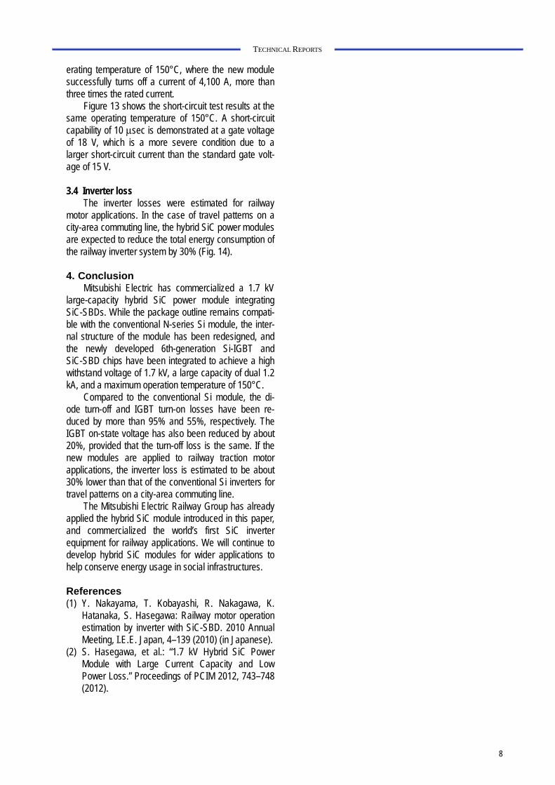
LVIC: lower arm IGBT drive circuit, under-voltage protection circuit for the control power supply, LVIC analog temperature output circuit, short-circuit protec-tion circuit (for short-circuit protection, an external cur-rent detection resistor is connected to the emitter sense (VSC) terminal of the lower arm IGBT, and when the voltage exceeds the specified threshold voltage, the lower arm IGBTs are turned off.) (3) Internal structure
Figure 3 shows a cross-sectional diagram of the 1,200 V Large DIPIPM Ver. 4. The internal structure is configured as follows: power chips, i.e., IGBT and FWD, and control IC chips, i.e., HVIC and LVIC are assem-bled on a lead frame. Connections are made between the chips using Al wires and Au wires. An aluminum heat sink and insulated heat dissipation sheet are put together, and then transfer-molded to complete the package.
Fig. 3 Internal structure of 1,200 V Large DIPIPM Ver. 4
3. Features of 1,200 V/50 A Large DIPIPM
Ver. 4 The newly developed 1,200 V/50 A Large DIPIPM
Ver. 4 model PS22A79 has the following features.
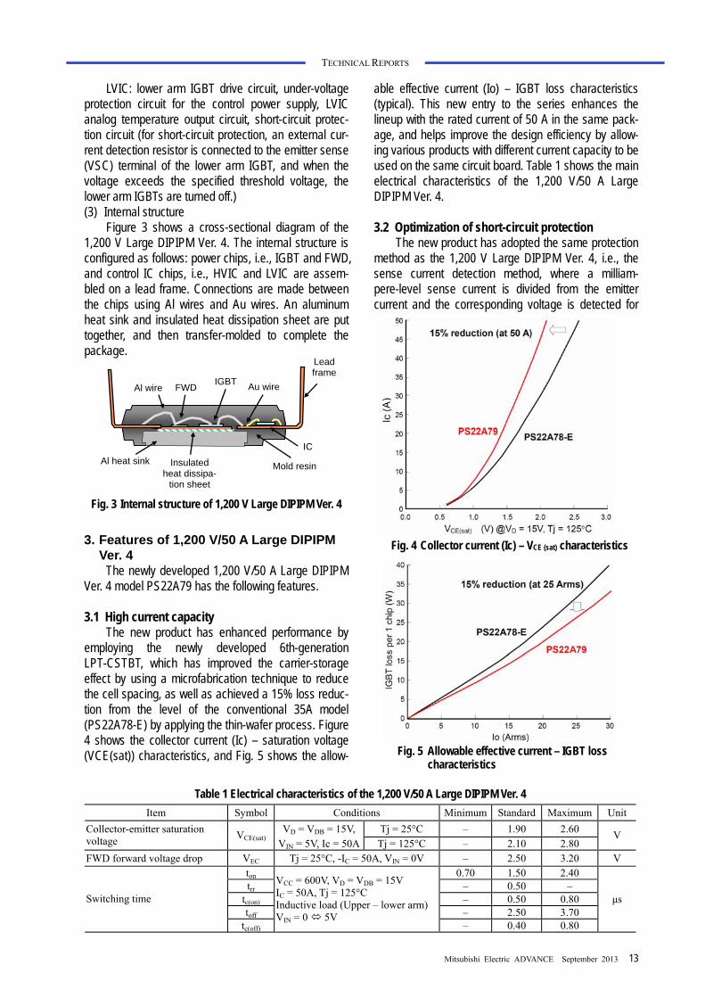
3.1 High current capacity The new product has enhanced performance by
employing the newly developed 6th-generation LPT-CSTBT, which has improved the carrier-storage effect by using a microfabrication technique to reduce the cell spacing, as well as achieved a 15% loss reduc-tion from the level of the conventional 35A model (PS22A78-E) by applying the thin-wafer process. Figure 4 shows the collector current (Ic) – saturation voltage (VCE(sat)) characteristics, and Fig. 5 shows the allow-
able effective current (Io) – IGBT loss characteristics (typical). This new entry to the series enhances the lineup with the rated current of 50 A in the same pack-age, and helps improve the design efficiency by allow-ing various products with different current capacity to be used on the same circuit board. Table 1 shows the main electrical characteristics of the 1,200 V/50 A Large DIPIPM Ver. 4.
3.2 Optimization of short-circuit protection
The new product has adopted the same protection method as the 1,200 V Large DIPIPM Ver. 4, i.e., the sense current detection method, where a milliam-pere-level sense current is divided from the emitter current and the corresponding voltage is detected for
Insulated heat dissipa-
tion sheet
Au wire FWD
Al heat sink
IGBT Al wire
Lead frame
IC
Mold resin
Fig. 5 Allowable effective current – IGBT loss characteristics
Table 1 Electrical characteristics of the 1,200 V/50 A Large DIPIPM Ver. 4
Item Symbol Conditions Minimum Standard Maximum Unit
VD = VDB = 15V, Tj = 25°C – 1.90 2.60 Collector-emitter saturation voltage
VCE(sat) VIN = 5V, Ic = 50A Tj = 125°C – 2.10 2.80
V
FWD forward voltage drop VEC Tj = 25°C, -IC = 50A, VIN = 0V – 2.50 3.20 V ton 0.70 1.50 2.40 trr – 0.50 –
tc(on) – 0.50 0.80 μs toff – 2.50 3.70
Switching time
tc(off)
VCC = 600V, VD = VDB = 15V IC = 50A, Tj = 125°C Inductive load (Upper – lower arm) VIN = 0 5V
– 0.40 0.80
Fig. 4 Collector current (Ic) – VCE (sat) characteristics

14
TECHNICAL REPORTS
protection. To obtain the sense current, IGBTs with an on-chip current sensor are used for the lower arm power chips. Since the shunt resistor inserted into the emitter current path is no longer needed, an induc-tance-induced surge voltage across the NU/NV/NW terminals and VNC terminal can be suppressed, result-ing in increased flexibility of circuit board design. In addition, to detect ampere-level emitter current, a high-wattage-type shunt resistor is required, but the sense current detection method can reduce the loss and increase the flexibility of the shunt resistor selection.
3.3 Precision improvement of temperature
detection The temperature detection function, which has al-
ready been integrated in the conventional series, has a temperature detector built into the control IC (LVIC) and provides an output of the analog voltage signal. This function eliminates the need for the external thermistor and reduces the system cost. This time, by using laser trimming technology, the output characteristics of the analog voltage signal have been made adjustable, resulting in higher precision of the output. When the analog voltage signal is used to control the junction temperature of the IGBT chip below a certain tempera-ture, variance in the signal needs to be considered; therefore, if the temperature precision is low, the normal operating range of the device needs to be narrowed. The improved precision allows operation at almost the maximum rating condition, and helps mitigate the re-quirements for the heat dissipation design and reduction of size. Figures 6 and 7 show the analogue temperature output VOT versus LVIC temperature characteristics for the conventional and new product, respectively.
4. Conclusion
This paper has presented the structure, functions, and features of the newly developed 1,200 V/50 A Large DIPIPM Ver. 4. We will extend the application of the developed technologies and increase the current capacity to enhance the lineup. We will also continue to provide the inverter market with advanced products by integrating bootstrap diodes to contribute to global environmental conservation.
References (1) T. Takahashi, et al: “The 6th-Generation IGBT &
Thin Wafer Diode for New Power Module”, Mitsu-bishi Denki Giho, 84, No. 4, 224–227 (2010) (in Japanese).
(2) H. Kawafuji, et al.: “New 5-35A/1200V Transfer Mold IPM with heat dissipating insulation sheet”, PCIM (2008).
Fig. 6 Analogue temperature output VOT vs. LVIC tem-perature characteristics (Conventional product)
Fig. 7 Analogue temperature output VOT vs. LVIC
temperature characteristics (New product)

*Power Device Works Mitsubishi Electric ADVANCE September 2013 15
TECHNICAL REPORTS
The IGBT Module for Three-Level Bidirectional Switch Type Inverter
Authors: Satoshi Kawabata*, Hiroki Muraoka* and Ayumi Maruta*
1. Introduction
Three-level inverters inherently have higher effi-ciency than the standard two-level configuration. This paper presents an insulated gate bipolar transistor (IGBT) module that integrates bidirectional switches for three-level bidirectional switch type inverter applications. By employing Mitsubishi Electric’s newest 6th-generation IGBT, this product helps users simplify the circuit configuration and improve its efficiency.
2. Product Concept
We have developed this product based on the concept of Mitsubishi Electric’s newest 6th-generation IGBT with the goal of integrating bidirectional switches for three-level inverters into the conventional NF Series package.
3. Product Specifications
Figures 1 and 2 respectively show the outline view and circuit diagram of the module.
Fig. 1 Outline
Fig. 2 Circuit diagram
The 6th-generation IGBT has a wide operating
temperature range up to the maximum junction tem-perature of 175°C, which is 25°C higher than that of the 5th-generation IGBT of 150°C, and thus provides users with more flexibility of temperature design.
In the three-level bidirectional switch topology, the voltage applied to each IGBT during the switching period is generally one-half that of the two-level topol-ogy. However, considering high-voltage applications, the chip was designed to have a breakdown voltage of 1,200 V. This also gives a margin against a surge volt-age induced by the circuit wiring inductance and ap-plied to the chip.
These features provide an easy-to-design device for the users.
4. Circuit Configuration of Three-Level
Inverter
4.1 Features Figure 3 illustrates various circuit configurations of
electric power inverters. Figure 3 (a) through (c) shows the standard two-level, three-level neutral point clamped (NPC), and three-level bidirectional switch topologies, respectively. The two-level circuit gives an output voltage with a stepwise change equal to the direct current voltage of E, whereas the three-level topologies give a stepwise change of E/2, which pro-vides an output voltage closer to a sine wave, and thus the size of filter circuit can be reduced. A breakdown voltage of the elements for the three-level NPC topol-ogy can be one-half that of the two-level topology, and thus the three-level NPC topology is a suitable configu-ration for high-voltage power converters. For improved efficiency, however, the three-level bidirectional switch topology is more advantageous than the NPC topology. In the NPC configuration, at an output voltage of P (or N), the current passes through the elements Q11 and Q12 (or D13 and D14), whereas in the bidirectional switch configuration, it is only Q11 (or D14), that is, the number of elements that the current passes through is one half, and thus the conduction loss can be reduced.
4.2 Loss of Three-Level Bidirectional Switch Type
Figure 4 shows a relative comparison of the IGBT loss between two circuit configurations, where the direct current voltage, output current and switching frequency are the same. The loss in the two-level configuration is dominated by switching loss, accounting for about 70%. In contrast, in the three-level bidirectional switch con-figuration, the voltage applied during the switching

16
TECHNICAL REPORTS
(a) Two-level circuit
(b) Three-level neutral point clamped topology
(c) Three-level bidirectional switch topology
Fig. 3 Circuit
Fig. 4 Element loss ratio by circuit
period becomes E/2, which significantly reduces the switching loss and hence the total loss by about 35%.
5. Application Examples The three-level bidirectional switch configuration
with the 6th-generation IGBTs was applied to the con-verter and inverter of an uninterruptible power supply (UPS). The efficiency was improved by about 2% com-pared to the two-level circuit configuration with the 5th-generation IGBTs. Figure 5 shows a relative com-parison of the conversion efficiency.
90%
92%
94%
96%
98%
100%
0% 20% 40% 60% 80% 100% 120%
Load factor (%)E
ffic
ien
cy (
%)
Two-level circuit (5th-generation IGBT)
Three-level bidirectional switch topology (6th-generation IGBT)
Fig. 5 Equipment efficiency curve at 400 V/500 kVA
The three-level bidirectional switch type inverter
has achieved high efficiency of over 96% in the load factor range from 20% to 100%, and the maximum efficiency is over 97%, which is about 2% higher than that of the standard two-level type inverter.
6. Conclusion
Mitsubishi Electric’s newest 6th-generation IGBTs and three-level bidirectional switch configuration are expected to help improve equipment efficiency. With continuous product development, we will enhance the lineup of the 6th-generation IGBTs to enable users to simplify their circuit configurations.

*Power Device Works Mitsubishi Electric ADVANCE September 2013 17
TECHNICAL REPORTS
“J-Series” IPM and T-PM for EV and HEV Applications
Authors: Seiichiro Inokuchi* and Mikio Ishihara*
1. Introduction
There is a growing demand for power semiconduc-tors applied to motor drive inverters for electric vehicles (EVs) and hybrid electric vehicles (HEVs). Based on the results of the development and mass production of automotive power semiconductors, which require very high reliability and functionality, Mitsubishi Electric has developed the J-Series Intelligent Power Modules (IPMs) and J-Series Transfer-Molded Power Modules (T-PMs) for multipurpose automotive applications.
2. J-Series IPM
The J-Series IPMs are designed for automotive applications, providing both high functionality and reli-ability required for automotive power modules. The J-Series line-up offers six models: Type-A (600 V/300 A, 1,200 V/150 A), Type-B (600 V/600 A, 1,200 V/300 A), and Type+B (600 V/800 A, 1,200 V/500 A) (Fig. 1). Each module is configured in an all-in-one package consisting of six sets of IGBTs and diodes, IGBT drive circuit, protection circuit, isolation circuit, and in-put-output processing circuit. The 600 V/800 A and 1,200 V/500 A models are equipped with a built-in power supply circuit, as well. These IPMs enable cus-tomers to enhance the functionality and reliability of their automotive inverter system and to improve the development efficiency.
Type-A
Type-B Type+B
Fig. 1 J-Series IPM Figure 2 shows the internal structure of the
J-Series IPM Type-A. Lead-free solder is used to com-ply with the End of Life Vehicles (ELV) Directive. For ease of attachment by the user, the base plate is de-
signed flat and made of a copper-based material with good thermal conductivity. In addition, a shielding plate is inserted to shield against radiation noise from the IGBT to the IPM control board and the inverter. For connection to the customer’s upper system, an automo-tive connector has been employed considering ease of assembly and vibration resistance. Furthermore, the analytical result of the structure under vibration has been considered in the design to improve the vibration resistance of the control board and entire IPM structure.
Lid
Control board
Shielding
Case
Base plate
Isolated board
plate
Fig. 2 Type-A structure
In addition to the drive circuit and protection circuit,
the J-Series IPM has also integrated the functions of IPM RDY, chip temperature monitoring, and DC-Link voltage monitoring (option at order). Protection functions are provided for over-current, over-temperature, and con-trol-power-supply under-voltage. The over-current pro-tection, in particular, employs a quick-response on-chip current sensor to ensure that the IGBT safely operates below its saturation current (Fig. 3).
VGE: Gate-Emitter Voltage IC: Collector Current VCE: Collector-Emitter Voltage ISC: Collector Current (with over-current Protection)
Fig. 3 Short circuit protection curve (example)

18
TECHNICAL REPORTS
The IPM RDY function allows input and output of the IPM ready signal. When an error occurs, the customer’s system can directly shut down the IPM by sending an “inoperable” signal. The chip temperature monitoring function provides an analog output (Tout) to indicate the surface temperature at the chip center. Compared to the temperature monitoring with a thermistor on the base plate, it gives a higher accuracy and linear output in the normal to high temperature range, which is advanta-geous for IPM protection, adjustment of inverter load and other controls. The DC-Link voltage monitoring function provides an analog output (VDCout) to indicate the volt-age across the IPM’s main P and N terminals, which helps to provide high functionality such as the battery management function. The primary and secondary cir-cuits are isolated using mass production proven photo-couplers. The Tout and VDCout signals are also isolated by the photo-couplers so that they can be safely utilized in the customer’s system. Regarding electro-magnetic compatibility (EMC), high noise immunity has been achieved by employing the current drive method for the input signals and optimizing the circuit board pattern.
Excellent reliability has been achieved, demon-strating thermal and power cycle resistance, respec-tively, 5–10 times and 1.5–2 times that of general in-dustrial products. In addition, reliability of the control board has been verified specifically for automotive applications such as through high-temperature and high-humidity bias tests.
The J-Series offers all-in-one IPMs that allow high functionality and safety design of the inverters for automotive applications.
3. J-Series T-PM
The J-Series T-PMs are high capacity power mod-ules fabricated in a transfer-molded package developed for automotive applications. The line-up offers three models, 300 A/600 V, 600 A/600 V and 300 A/1,200 V, in the same package size (Fig. 4). For user’s T-PM evaluation purposes, evaluation kits are also available. The J-Series T-PMs are completely lead-free products with a low environmental burden.
Fig. 4 J-Series T-PM (CT300DJH060)
Figure 5 shows a schematic structure of the J-Series T-PM. The rear surfaces of the power chips (IGBT and diode) are soldered to the heat spreader. The front surfaces are directly soldered to the inner lead, which is extended from the main terminal, to form the main circuit wiring structure referred to as a direct lead bonding (DLB) structure. Compared to the conven-tional main circuit structure using aluminum wire bond-ing, the DLB structure has achieved: (1) lower wiring resistance, (2) lower self inductance, and (3) longer power cycle life (to be described later). Thermally Con-ductive electrically Isolated Layer (TCIL) has been inserted beneath the bottom surface of the heat spreader, and the sheet material was selected so that it has heat conductivity higher than that of the mold resin. The thermal resistance has been reduced with this configuration, where the heat generated by the chips is spread by the heat spreader, and then passes through the TCIL. In addition, the transient thermal resistance has also been reduced by directly connecting the chips to the heat spreader having a large heat capacity. These internal structures are encapsulated by the mold resin to ensure the mechanical structure, strength, insulation, and environmental durability for the module.
The thermal and power cycle performance of the J-Series T-PMs is more than 30 times that of Mitsubishi Electric’s industrial case-type modules. The lifetime in thermal cycling test is determined by the thermal strain in the solder beneath the chips. The J-Series T-PM module has reduced the strain and hence achieved long lifetime by employing the resin encapsulation structure and making the coefficient of thermal expan-sion of the mold resin close to that of the heat spreader (Fig. 6). The lifetime in power cycling test has also been improved by employing the DLB structure for the inter-nal main circuit wiring, which has eliminated the peeling problem of aluminum wires experienced with the con-ventional case-type modules.
Fig. 5 J-Series T-PM structure
Heat spreader
Resin
Chip
Solder
Fig. 6 Reduction of strain in solder joint by resin
covering

Mitsubishi Electric ADVANCE September 2013 19
TECHNICAL REPORTS
4. Conclusion We have developed the “J-Series” IPMs and
T-PMs, automotive power devices for HEV and EV applications. The “J-Series” is expected to meet the various needs of customers and contribute to an envi-ronmentally conscious society. We will continue to enhance the product line-up, striving for higher func-tionality, higher reliability and lighter weight.