Embed Size (px)
Citation preview
SI MICRO PROBE AND SIO2 MICRO TUBE ARRAY INTEGRATED WITH NMOSFETS
Kuniharu Takei, Takahiro Kawashima, Hidekuni Takao, Kazuaki Sawada, and Makoto Ishida Transducers’07
Presenter:Wen-Fan Liao
ID: g946220
Instructor: Cheng-Hsien Liu
Outline
Introduction Process Results Conclusion References
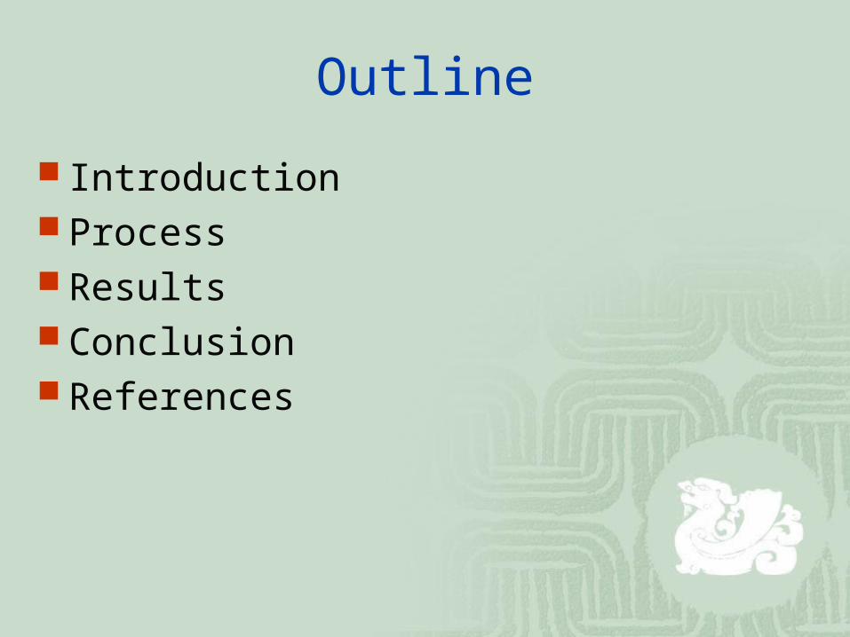
Introduction
Neural activity recording is important to analyze neural networks
Recording site and invasiveness are issues Proposed micro probes and tube array for neural p
enetrating devices fabricated by Vapor-Liquid-Solid (VLS) method
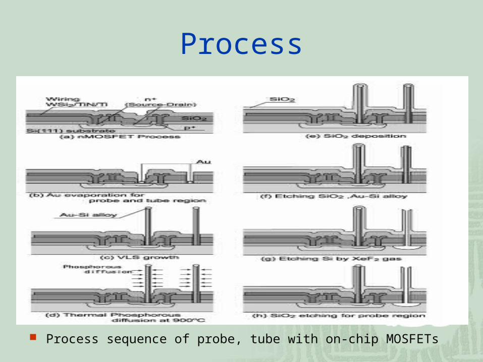
Process
Process sequence of probe, tube with on-chip MOSFETs
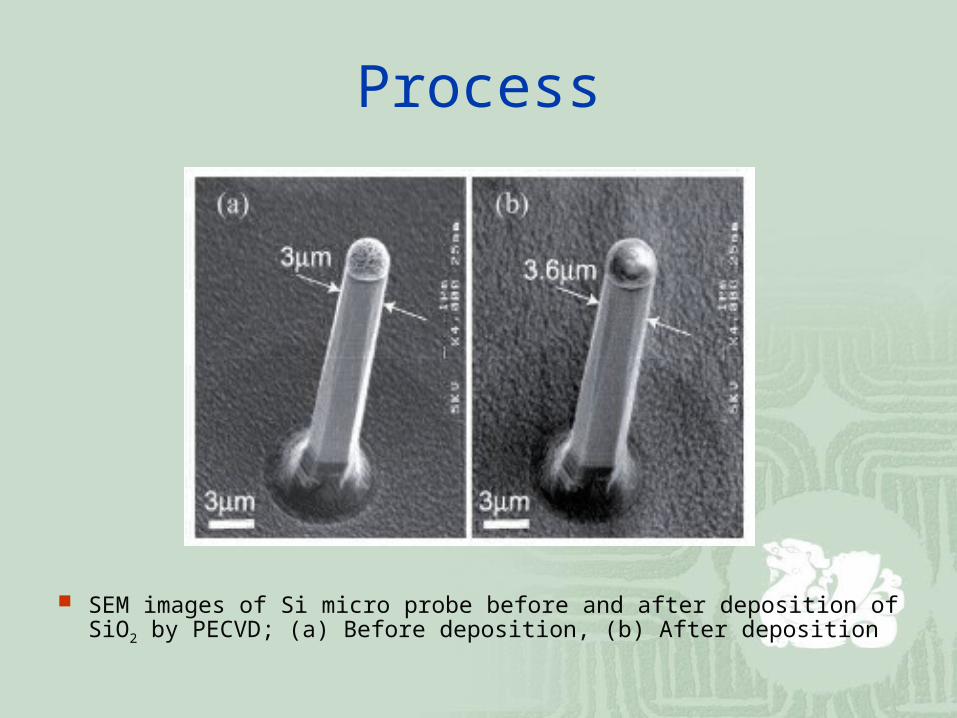
Process
SEM images of Si micro probe before and after deposition of SiO2 by PECVD; (a) Before deposition, (b) After deposition
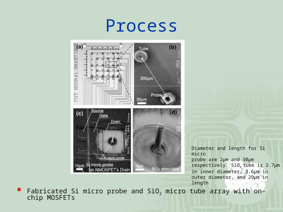
Process
Fabricated Si micro probe and SiO2 micro tube array with on-chip MOSFETs
Diameter and length for Si microprobe are 2μm and 30μm respectively. SiO2 tube is 2.7μm in inner diameter, 3.6μm in outer diameter, and 29μm in length
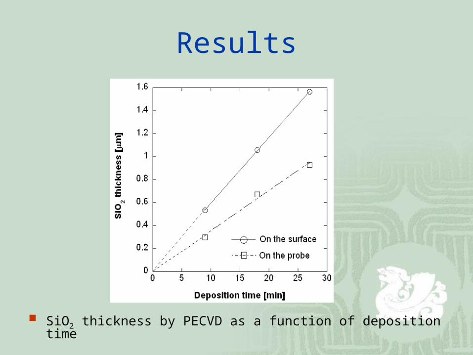
Results
SiO2 thickness by PECVD as a function of deposition time
Results
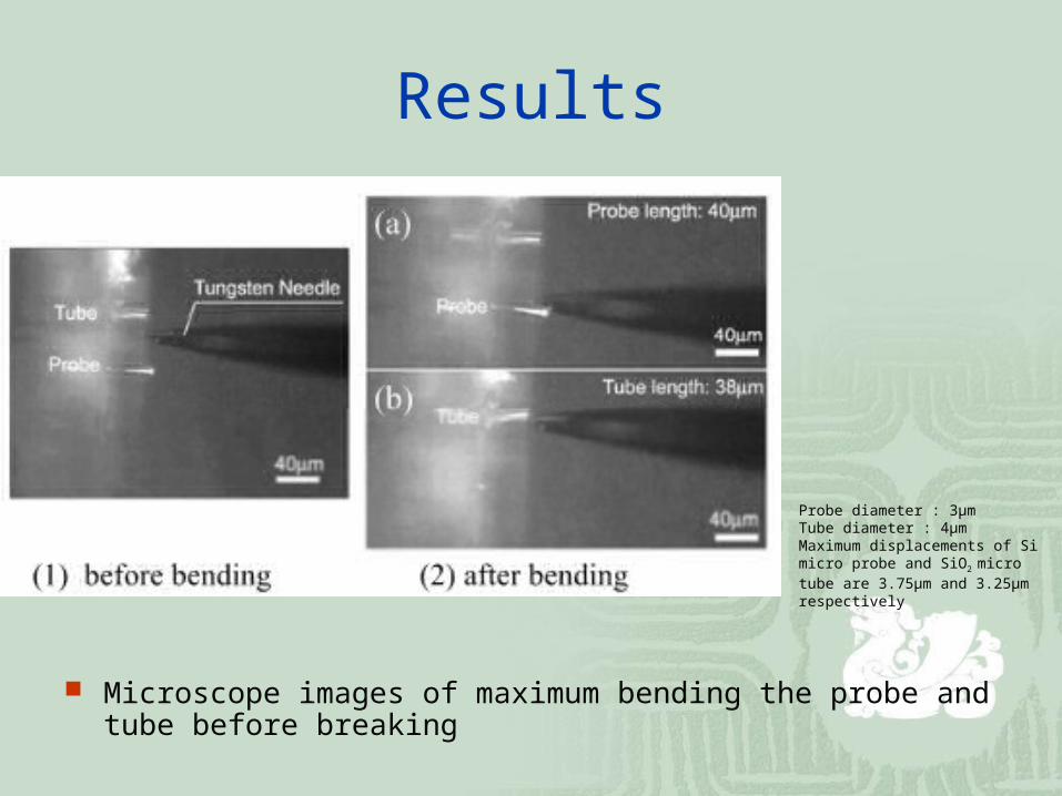
Microscope images of maximum bending the probe and tube before breaking
Probe diameter : 3μmTube diameter : 4μmMaximum displacements of Si micro probe and SiO2 micro tube are 3.75μm and 3.25μm respectively
Results
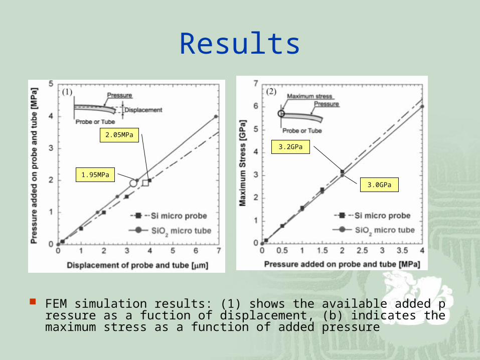
FEM simulation results: (1) shows the available added pressure as a fuction of displacement, (b) indicates the maximum stress as a function of added pressure
1.95MPa
2.05MPa
3.0GPa
3.2GPa
Results
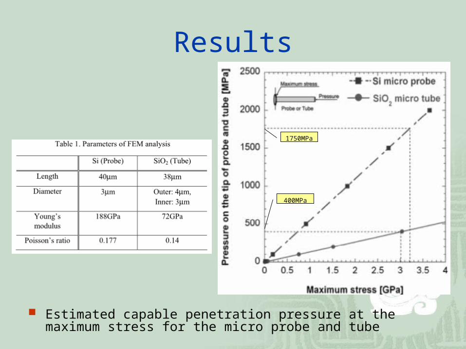
Estimated capable penetration pressure at the maximum stress for the micro probe and tube
1750MPa
400MPa
Results
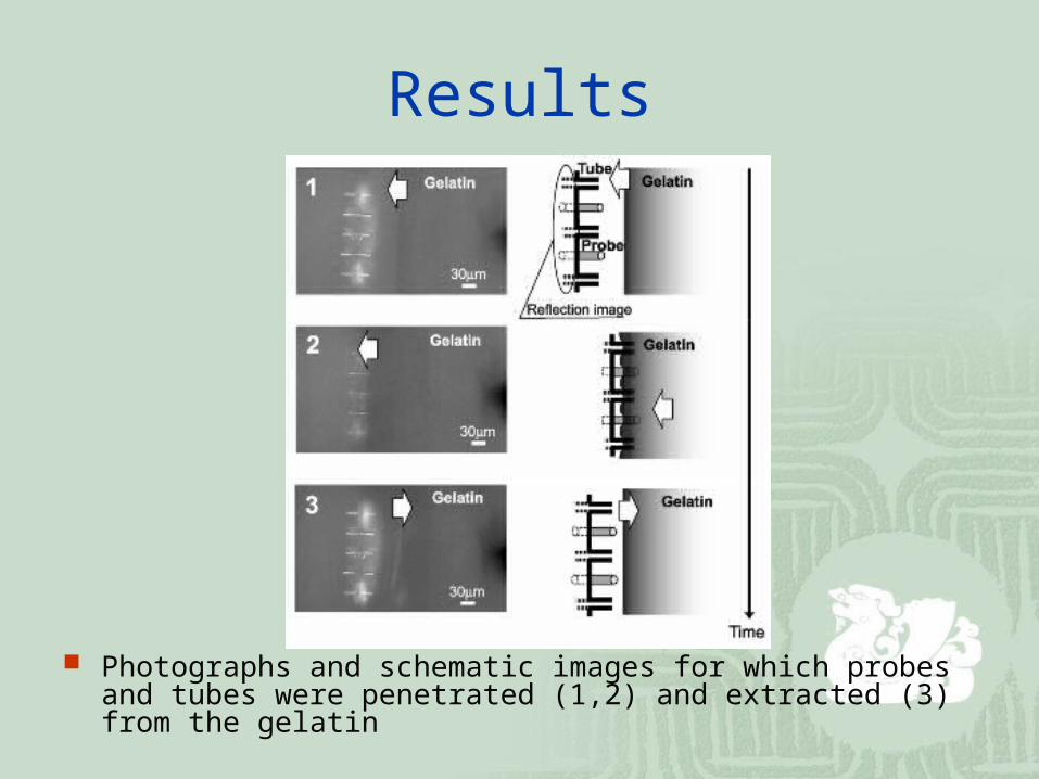
Photographs and schematic images for which probes and tubes were penetrated (1,2) and extracted (3) from the gelatin
Conclusion
This work reports the development of Si micro probe and SiO2 micro tube array with on-chip MOSFETs for a neural recording device
This device is expected to be suitable for analysis of neural behavior with low invasiveness, which can be applied in neuron science or other applications
References Kuniharu Takei, Takahiro Kawashima, Hidekuni Takao, Kazuaki Sawa
da, and Makoto Ishida, “SI MICRO PROBE AND SIO2 MICRO TUBE ARRAY INTEGRATED WITH NMOSFETS,” Transducers’07, Lyon, France, June 2007
Kuniharu Takei, Takahiro Kawashima, Kazuaki Sawada, and Makoto Ishida, “MECHANICAL PROPERTIES OF MICRO PROBE AND TUBE ARRAY FOR NEURAL PENETRATING DEVICES,” Engineering in Medicine and Biology Society, 2007. EMBS 2007. 29th Annual International Conference of the IEEE
http://www.mems.nthu.edu.tw/nano/071228_MEMS neuroscience.ppt

~Thank you for your attention~