Embed Size (px)
Citation preview
Rev. 2.7 Page 1 2011-09-27
SPP17N80C3SPA17N80C3
Cool MOS™ Power Transistor VDS 800 V
RDS(on) 0.29 Ω
ID 17 A
Feature
• New revolutionary high voltage technology
• Worldwide best RDS(on) in TO 220
• Ultra low gate charge
• Periodic avalanche rated
• Extreme dv/dt rated
• Ultra low effective capacitances
• Improved transconductance
• PG-TO-220-3-31: Fully isolated package (2500 VAC; 1 minute)
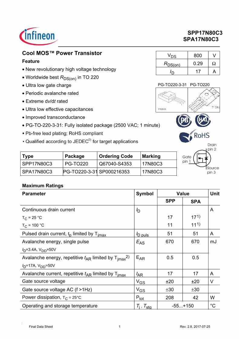
PG-TO220-3-31 PG-TO220
P-TO220-3-31
12
3
Marking
17N80C3
17N80C3
Type Package Ordering Code
SPP17N80C3 PG-TO220 Q67040-S4353
SPA17N80C3 PG-TO220-3-31 SP000216353
Maximum Ratings
Parameter Symbol Value Unit
SPA
Continuous drain current
TC = 25 °C
TC = 100 °C
ID
17
11
171)
111)
A
Pulsed drain current, tp limited by Tjmax ID puls 51 51 A
Avalanche energy, single pulse
ID=3.4A, VDD=50V
EAS 670 670 mJ
Avalanche energy, repetitive tAR limited by Tjmax2)
ID=17A, VDD=50V
EAR 0.5 0.5
Avalanche current, repetitive tAR limited by Tjmax IAR 17 17 A
Gate source voltage VGS ±20 ±20 V
Gate source voltage AC (f >1Hz) VGS ±30 ±30
Power dissipation, TC = 25°C Ptot 208 42 W
SPP
Operating and storage temperature Tj , Tstg -55...+150 °C
Final Data Sheet 1 Rev. 2.8, 2017-07-25
Rev. 2.7 Page 2 2011-09-27
SPP17N80C3SPA17N80C3
Maximum Ratings
Parameter Symbol Value Unit
Drain Source voltage slope
VDS = 640 V, ID = 17 A, Tj = 125 °C
dv/dt 50 V/ns
Thermal Characteristics
Parameter Symbol Values Unit
min. typ. max.
Thermal resistance, junction - case RthJC - - 0.6 K/W
Thermal resistance, junction - case, FullPAK RthJC_FP - - 3.6
Thermal resistance, junction - ambient, leaded RthJA - - 62
Thermal resistance, junction - ambient, FullPAK RthJA_FP - - 80
SMD version, device on PCB:
@ min. footprint
@ 6 cm2 cooling area 3)
RthJA
-
-
-
35
62
-
Soldering temperature, wavesoldering
1.6 mm (0.063 in.) from case for 10s 4)
Tsold - - 260 °C
Electrical Characteristics, at Tj=25°C unless otherwise specified
Parameter Symbol Conditions Values Unit
min. typ. max.
Drain-source breakdown voltage V(BR)DSS VGS=0V, ID=0.25mA 800 - - V
Drain-Source avalanche
breakdown voltage
V(BR)DS VGS=0V, ID=17A - 870 -
Gate threshold voltage VGS(th) ID=1000µA, VGS=VDS 2.1 3 3.9
Zero gate voltage drain current IDSS VDS=800V, VGS=0V,
Tj=25°C
Tj=150°C
-
-
0.5
-
25
250
µA
Gate-source leakage current IGSS VGS=20V, VDS=0V - - 100 nA
Drain-source on-state resistance RDS(on) VGS=10V, ID=11A
Tj=25°C
Tj=150°C
-
-
0.25
0.78
0.29
-
Ω
Gate input resistance RG f=1MHz, open drain - 0.7 -
Final Data Sheet 2 Rev. 2.8, 2017-07-25
Rev. 2.7 Page 3 2011-09-27
SPP17N80C3SPA17N80C3
Electrical Characteristics
Parameter Symbol Conditions Values Unit
min. typ. max.
Transconductance gfs VDS≥2*ID*RDS(on)max,
ID=11A
- 15 - S
Input capacitance Ciss VGS=0V, VDS=25V,
f=1MHz
- 2320 - pF
Output capacitance Coss - 1250 -
Reverse transfer capacitance Crss - 60 -
Effective output capacitance,5)
energy related
Co(er) VGS=0V,
VDS=0V to 480V
- 59 -
Effective output capacitance,6)
time related
Co(tr) - 124 -
Turn-on delay time td(on) VDD=400V, VGS=0/10V,
ID=17A,
RG=4.7Ω, Tj=125°C
- 25 - ns
Rise time tr - 15 -
Turn-off delay time td(off) - 72 82
Fall time tf - 6 9
Gate Charge Characteristics
Gate to source charge Qgs VDD=640V, ID=17A - 12 - nC
Gate to drain charge Qgd - 46 -
Gate charge total Qg VDD=640V, ID=17A,
VGS=0 to 10V
- 91 177
Gate plateau voltage V(plateau) VDD=640V, ID=17A - 6 - V
1Limited only by maximum temperature
2Repetitve avalanche causes additional power losses that can be calculated as PAV=EAR*f.
3Device on 40mm*40mm*1.5mm epoxy PCB FR4 with 6cm² (one layer, 70 µm thick) copper area for drain
connection. PCB is vertical without blown air.
4Soldering temperature for TO-263: 220°C, reflow
5Co(er) is a fixed capacitance that gives the same stored energy as Coss while VDS is rising from 0 to 80% VDSS.
6Co(tr) is a fixed capacitance that gives the same charging time as Coss while VDS is rising from 0 to 80% VDSS.
Final Data Sheet 3 Rev. 2.8, 2017-07-25
Rev. 2.7 Page 4 2011-09-27
SPP17N80C3SPA17N80C3
Electrical Characteristics
Parameter Symbol Conditions Values Unit
min. typ. max.
Inverse diode continuous
forward current
IS TC=25°C - - 17 A
Inverse diode direct current,
pulsed
ISM - - 51
Inverse diode forward voltage VSD VGS=0V, IF=IS - 1 1.2 V
Reverse recovery time trr VR=400V, IF=IS ,
diF/dt=100A/µs
- 550 - ns
Reverse recovery charge Qrr - 15 - µC
Peak reverse recovery current Irrm - 51 - A
Peak rate of fall of reverse
recovery current
dirr/dt Tj=25°C - 1200 - A/µs
Typical Transient Thermal Characteristics
Symbol Value Unit Symbol Value Unit
SPA SPA
Rth1 0.00812 0.00812 K/W Cth1 0.0003562 0.0003562 Ws/K
Rth2 0.016 0.016 Cth2 0.001337 0.001337
Rth3 0.031 0.031 Cth3 0.001831 0.001831
Rth4 0.114 0.16 Cth4 0.005033 0.005033
Rth5 0.135 0.324 Cth5 0.012 0.008657
Rth6 0.059 2.522 Cth6 0.092 0.412
SPP SPP
External HeatsinkT j Tcase
Tamb
C th1 C th2
R th1 R th,n
C th,n
P tot (t)
Final Data Sheet 4 Rev. 2.8, 2017-07-25
Rev. 2.7 Page 5 2011-09-27
SPP17N80C3SPA17N80C3
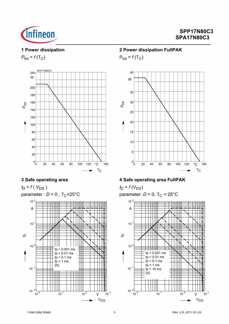
1 Power dissipation
Ptot = f (TC)
0 20 40 60 80 100 120 °C 160
TC
0
20
40
60
80
100
120
140
160
180
200
W
240SPP17N80C3
Pto
t
2 Power dissipation FullPAK
Ptot = f (TC)
0 20 40 60 80 100 120 °C 160
TC
0
5
10
15
20
25
30
35
W
45
Pto
t
3 Safe operating area
ID = f ( VDS )
parameter : D = 0 , TC=25°C
100
101
102
103
V
VDS
-210
-110
010
110
210
A
I D
tp = 0.001 ms
tp = 0.01 ms
tp = 0.1 ms
tp = 1 ms
DC
4 Safe operating area FullPAK
ID = f (VDS)
parameter: D = 0, TC = 25°C
100
101
102
103
V
VDS
-210
-110
010
110
210
A
I D
tp = 0.001 ms
tp = 0.01 ms
tp = 0.1 ms
tp = 1 ms
tp = 10 ms
DC
Final Data Sheet 5 Rev. 2.8, 2017-07-25
Rev. 2.7 Page 6 2011-09-27
SPP17N80C3SPA17N80C3
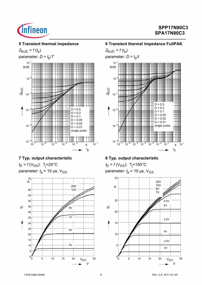
5 Transient thermal impedance
ZthJC = f (tp)
parameter: D = tp/T
10-7
10-6
10-5
10-4
10-3
10-1
s
tp
-410
-310
-210
-110
010
110
K/W
Zth
JC
D = 0.5
D = 0.2
D = 0.1
D = 0.05
D = 0.02
D = 0.01
single pulse
6 Transient thermal impedance FullPAK
ZthJC = f (tp)
parameter: D = tp/t
10-7
10-6
10-5
10-4
10-3
10-2
10-1
101
s
tp
-410
-310
-210
-110
010
110
K/W
Zth
JC
D = 0.5
D = 0.2
D = 0.1
D = 0.05
D = 0.02
D = 0.01
single pulse
7 Typ. output characteristic
ID = f (VDS); Tj=25°C
parameter: tp = 10 µs, VGS
0 5 10 15 20 VDS 30
V
0
5
10
15
20
25
30
35
40
45
50
55
60
A70
I D
5V
6V
7V
8V
20V
10V
8 Typ. output characteristic
ID = f (VDS); Tj=150°C
parameter: tp = 10 µs, VGS
0 5 10 15 20 VDS 30
V
0
5
10
15
20
25
A
35
I D
4V
4.5V
5V
5.5V
6V
6.5V
20V
10V
8V
7V
Final Data Sheet 6 Rev. 2.8, 2017-07-25
Rev. 2.7 Page 7 2011-09-27
SPP17N80C3SPA17N80C3
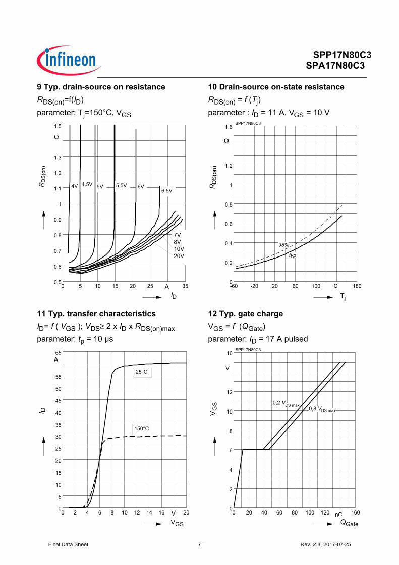
9 Typ. drain-source on resistance
RDS(on)=f(ID)
parameter: Tj=150°C, VGS
0 5 10 15 20 25 A 35
ID
0.5
0.6
0.7
0.8
0.9
1
1.1
1.2
1.3
Ω
1.5
RD
S(o
n)
4V 4.5V 5V 5.5V 6V6.5V
7V
8V
10V
20V
10 Drain-source on-state resistance
RDS(on) = f (Tj)
parameter : ID = 11 A, VGS = 10 V
-60 -20 20 60 100 °C 180
Tj
0
0.2
0.4
0.6
0.8
1
1.2
Ω
1.6SPP17N80C3
RD
S(o
n)
typ
98%
11 Typ. transfer characteristics
ID= f ( VGS ); VDS≥ 2 x ID x RDS(on)max
parameter: tp = 10 µs
0 2 4 6 8 10 12 14 16 V 20
VGS
0
5
10
15
20
25
30
35
40
45
50
55
A65
I D
25°C
150°C
12 Typ. gate charge
VGS = f (QGate)
parameter: ID = 17 A pulsed
0 20 40 60 80 100 120 nC 160
QGate
0
2
4
6
8
10
12
V
16SPP17N80C3
VG
S
0,8 VDS max
DS maxV0,2
Final Data Sheet 7 Rev. 2.8, 2017-07-25
Rev. 2.7 Page 8 2011-09-27
SPP17N80C3SPA17N80C3
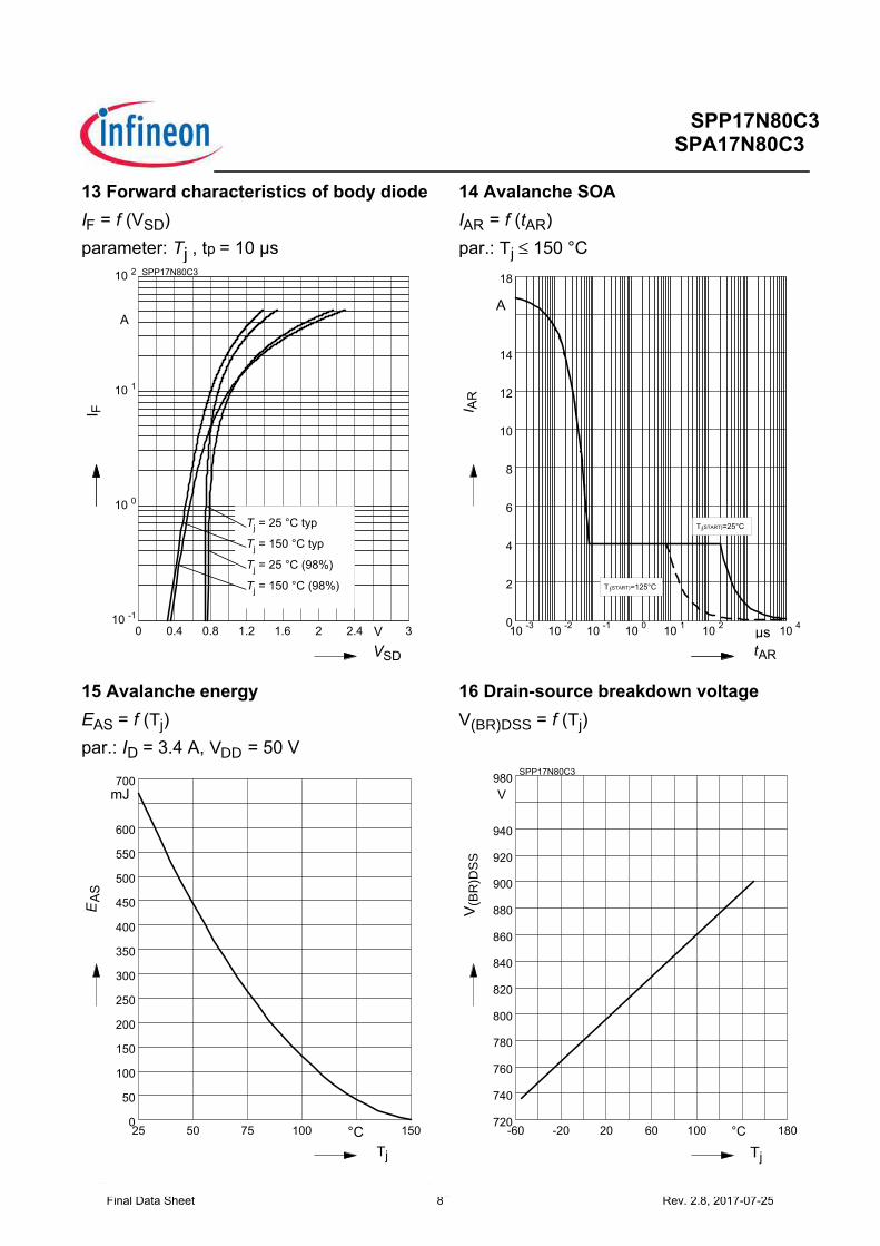
13 Forward characteristics of body diode
IF = f (VSD)
parameter: Tj , tp = 10 µs
0 0.4 0.8 1.2 1.6 2 2.4 V 3
VSD
-110
010
110
210
A
SPP17N80C3
I F
Tj = 25 °C typ
Tj = 25 °C (98%)
Tj = 150 °C typ
Tj = 150 °C (98%)
14 Avalanche SOA
IAR = f (tAR)
par.: Tj ≤ 150 °C
10-3
10-2
10-1
100
101
102
104
µs
tAR
0
2
4
6
8
10
12
14
A
18
I AR
T j(START)=125°C
T j(START)=25°C
15 Avalanche energy
EAS = f (Tj)
par.: ID = 3.4 A, VDD = 50 V
25 50 75 100 °C 150
Tj
0
50
100
150
200
250
300
350
400
450
500
550
600
mJ700
EA
S
16 Drain-source breakdown voltage
V(BR)DSS = f (Tj)
-60 -20 20 60 100 °C 180
Tj
720
740
760
780
800
820
840
860
880
900
920
940
V
980SPP17N80C3
V(B
R)D
SS
Final Data Sheet 8 Rev. 2.8, 2017-07-25
Rev. 2.7 Page 9 2011-09-27
SPP17N80C3SPA17N80C3
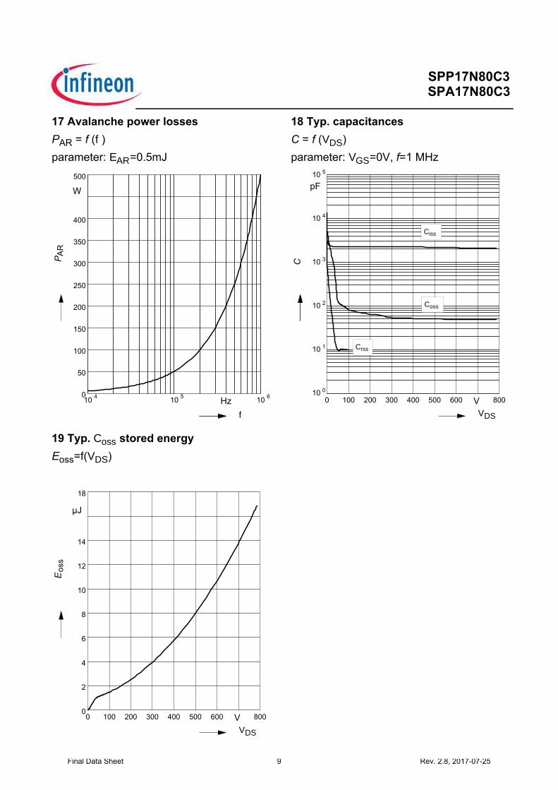
17 Avalanche power losses
PAR = f (f )
parameter: EAR=0.5mJ
104
105
106
Hz
f
0
50
100
150
200
250
300
350
400
W
500
PA
R
18 Typ. capacitances
C = f (VDS)
parameter: VGS=0V, f=1 MHz
0 100 200 300 400 500 600 V 800
VDS
010
110
210
310
410
510
pF
C
Ciss
Coss
Crss
19 Typ. Coss stored energy
Eoss=f(VDS)
0 100 200 300 400 500 600 V 800
VDS
0
2
4
6
8
10
12
14
µJ
18
Eo
ss
Final Data Sheet 9 Rev. 2.8, 2017-07-25
Rev. 2.7 Page 10 201109-27
SPP17N80C3 SPA17N80C3
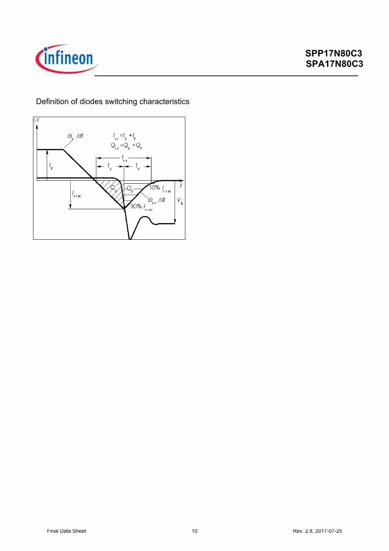
Definition of diodes switching characteristics
Final Data Sheet 10 Rev. 2.8, 2017-07-25
2011-09-27Rev. 2.7 Page 11
SPP17N80C3
SPA17N80C3
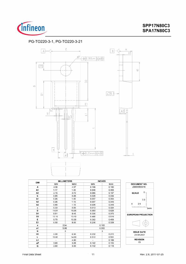
PG-TO220-3-1, PG-TO220-3-21
Final Data Sheet 11 Rev. 2.8, 2017-07-25
Final Datta Sheet 1 Rev. 2.2
SPP17N80SPA17N80
2, 2016‐08‐0
0C3 0C3
04
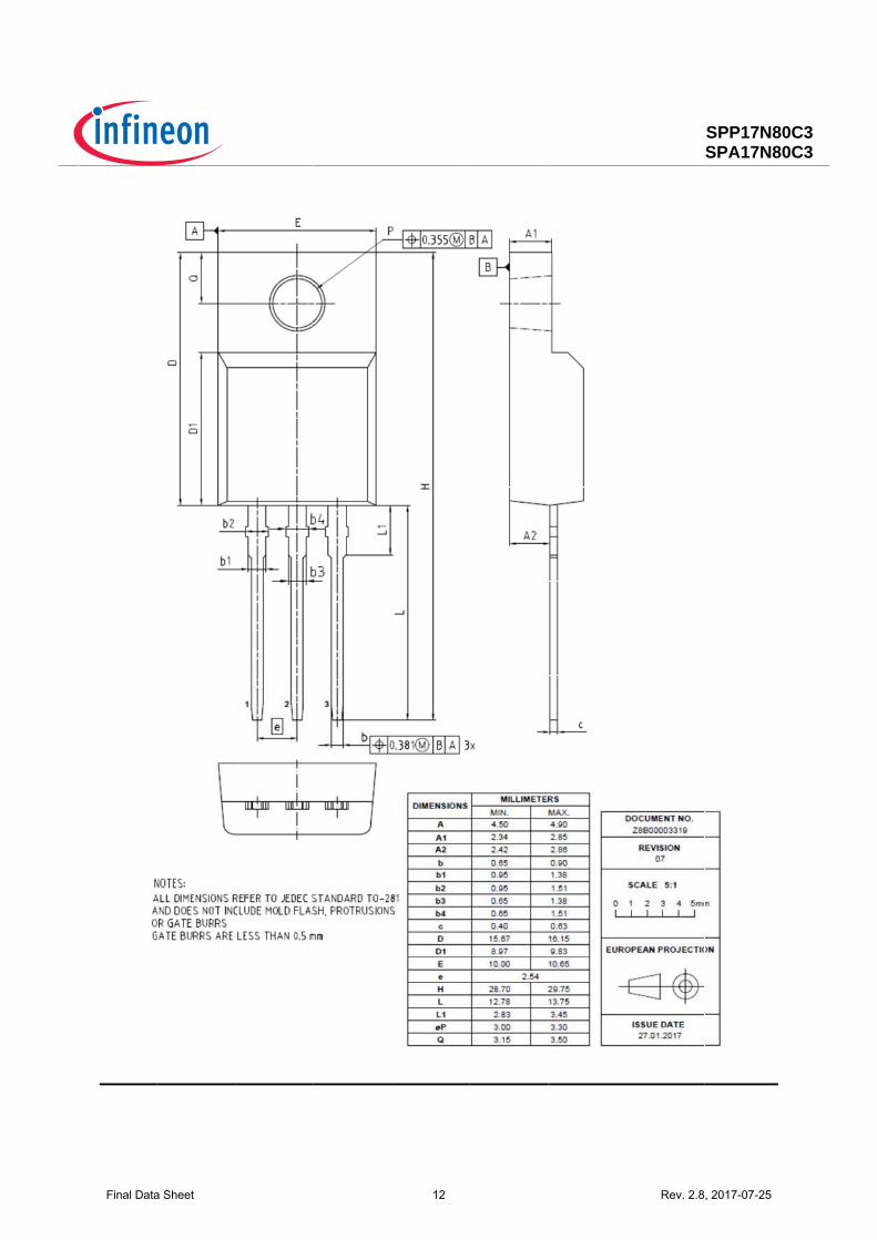
Final Data Sheet 12 Rev. 2.8, 2017-07-25
13
800VCoolMOSªC3PowerTransistorSPAl7N80C3
Rev.2.8,2017-07-27
RevisionHistorySPAl7N80C3
Revision:2017-07-27,Rev.2.8
Previous Revision
Revision Date Subjects (major changes since last revision)
2.8 2017-07-27 Revised package drawing on page 12
TrademarksofInfineonTechnologiesAG
AURIX™,C166™,CanPAK™,CIPOS™,CoolGaN™,CoolMOS™,CoolSET™,CoolSiC™,CORECONTROL™,CROSSAVE™,DAVE™,DI-POL™,DrBlade™,EasyPIM™,EconoBRIDGE™,EconoDUAL™,EconoPACK™,EconoPIM™,EiceDRIVER™,eupec™,FCOS™,HITFET™,HybridPACK™,Infineon™,ISOFACE™,IsoPACK™,i-Wafer™,MIPAQ™,ModSTACK™,my-d™,NovalithIC™,OmniTune™,OPTIGA™,OptiMOS™,ORIGA™,POWERCODE™,PRIMARION™,PrimePACK™,PrimeSTACK™,PROFET™,PRO-SIL™,RASIC™,REAL3™,ReverSave™,SatRIC™,SIEGET™,SIPMOS™,SmartLEWIS™,SOLIDFLASH™,SPOC™,TEMPFET™,thinQ™,TRENCHSTOP™,TriCore™.
TrademarksupdatedAugust2015
OtherTrademarks
Allreferencedproductorservicenamesandtrademarksarethepropertyoftheirrespectiveowners.
WeListentoYourCommentsAnyinformationwithinthisdocumentthatyoufeeliswrong,unclearormissingatall?Yourfeedbackwillhelpustocontinuouslyimprovethequalityofthisdocument.Pleasesendyourproposal(includingareferencetothisdocument)to:[email protected]
PublishedbyInfineonTechnologiesAG81726München,Germany©2017InfineonTechnologiesAGAllRightsReserved.
LegalDisclaimerTheinformationgiveninthisdocumentshallinnoeventberegardedasaguaranteeofconditionsorcharacteristics(“Beschaffenheitsgarantie”).
Withrespecttoanyexamples,hintsoranytypicalvaluesstatedhereinand/oranyinformationregardingtheapplicationoftheproduct,InfineonTechnologiesherebydisclaimsanyandallwarrantiesandliabilitiesofanykind,includingwithoutlimitationwarrantiesofnon-infringementofintellectualpropertyrightsofanythirdparty.Inaddition,anyinformationgiveninthisdocumentissubjecttocustomer’scompliancewithitsobligationsstatedinthisdocumentandanyapplicablelegalrequirements,normsandstandardsconcerningcustomer’sproductsandanyuseoftheproductofInfineonTechnologiesincustomer’sapplications.Thedatacontainedinthisdocumentisexclusivelyintendedfortechnicallytrainedstaff.Itistheresponsibilityofcustomer’stechnicaldepartmentstoevaluatethesuitabilityoftheproductfortheintendedapplicationandthecompletenessoftheproductinformationgiveninthisdocumentwithrespecttosuchapplication.
InformationForfurtherinformationontechnology,deliverytermsandconditionsandpricespleasecontactyournearestInfineonTechnologiesOffice(www.infineon.com).
WarningsDuetotechnicalrequirements,componentsmaycontaindangeroussubstances.Forinformationonthetypesinquestion,pleasecontactthenearestInfineonTechnologiesOffice.TheInfineonTechnologiescomponentdescribedinthisDataSheetmaybeusedinlife-supportdevicesorsystemsand/orautomotive,aviationandaerospaceapplicationsorsystemsonlywiththeexpresswrittenapprovalofInfineonTechnologies,ifafailureofsuchcomponentscanreasonablybeexpectedtocausethefailureofthatlife-support,automotive,aviationandaerospacedeviceorsystemortoaffectthesafetyoreffectivenessofthatdeviceorsystem.Lifesupportdevicesorsystemsareintendedtobeimplantedinthehumanbodyortosupportand/ormaintainandsustainand/orprotecthumanlife.Iftheyfail,itisreasonabletoassumethatthehealthoftheuserorotherpersonsmaybeendangered.