Embed Size (px)
Citation preview
Study of the HV/HR CMOS sensors for the ATLAS ITk and the CEPC silicon detectors
Jian LIU (刘剑) [email protected]
Supervisor: Prof. Meng WANG (王萌)
Shandong University
Chung-Yao Chao Fellowship Interview - IHEP, Beijing, 24 Apr 2017
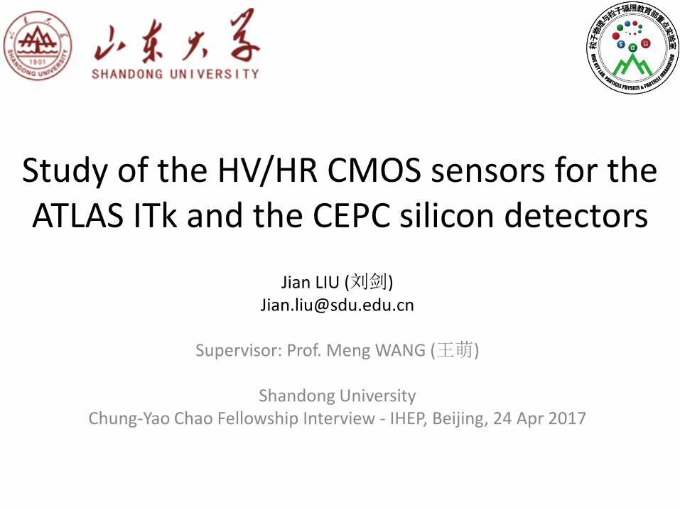
Outline
24/04/2017 J. LIU 2
• Resume
• Sensor simulation and characterization of the HV/HR CMOS sensors for the ATLAS ITk
• Research progress of the CMOS sensors for the CEPC silicon detectors and future plan
• Conclusion and perspectives
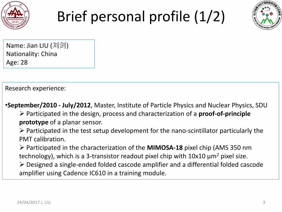
Brief personal profile (1/2)
24/04/2017 J. LIU
Name: Jian LIU (刘剑) Nationality: China Age: 28
Research experience: •September/2010 - July/2012, Master, Institute of Particle Physics and Nuclear Physics, SDU
Participated in the design, process and characterization of a proof-of-principle prototype of a planar sensor. Participated in the test setup development for the nano-scintillator particularly the PMT calibration. Participated in the characterization of the MIMOSA-18 pixel chip (AMS 350 nm technology), which is a 3-transistor readout pixel chip with 10x10 µm2 pixel size. Designed a single-ended folded cascode amplifier and a differential folded cascode amplifier using Cadence IC610 in a training module.
3
Brief personal profile (2/2)
24/04/2017 J. LIU
• September/2012 – June/2016, PhD candidate, CPPM/AMU and SDU, supervised by Prof. Meng WANG (SDU), Prof. Marlon BARBERO (CPPM) and Dr. Alexandre ROZANOV (CPPM) . Granted by SDU/FCPPL/Eiffel. Thesis: Study of a monolithic pixel detector for the ATLAS tracker at the High Luminosity LHC
Participated in the conceptual design of the HV/HR CMOS sensors. Contributed to the test setup development for the HV/HR CMOS sensors. Organized and participated in the characterizations for AMS 180 nm , GF 130 nm and LF 150 nm prototypes at CPPM and CERN. Contributed to the development of the calibration procedures for the FE-I4 Generic-GADC and performed the corresponding measurements. Qualified as ATLAS author since 2014. Participated in the 3D technology exploration. Measured the impedance of Through Silicon Via (TSV) and Bond Interface (BI) for the FE-TC4 chips. Probing test for the 3D wafers and chips. Performed the TCAD simulations for the TSV.
• September/2016 – now, postdoc fellow at SDU, supervisor: Prof. Meng WANG Responsible for the TCAD simulations for the radiation hard CMOS sensors. Responsible for the CMOS pixel detector test setup development. Investigating the suitable HV/HR CMOS technologies for the CEPC detector, particularly the Chinese semiconductor foundries.
4
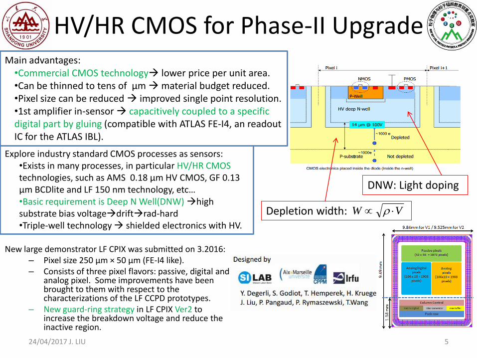
HV/HR CMOS for Phase-II Upgrade
24/04/2017 J. LIU
Explore industry standard CMOS processes as sensors: •Exists in many processes, in particular HV/HR CMOS technologies, such as AMS 0.18 µm HV CMOS, GF 0.13 µm BCDlite and LF 150 nm technology, etc… •Basic requirement is Deep N Well(DNW) high substrate bias voltagedriftrad-hard •Triple-well technology shielded electronics with HV.
DNW: Light doping
VW Depletion width:
5
Main advantages: •Commercial CMOS technology lower price per unit area. •Can be thinned to tens of µm material budget reduced. •Pixel size can be reduced improved single point resolution. •1st amplifier in-sensor capacitively coupled to a specific digital part by gluing (compatible with ATLAS FE-I4, an readout IC for the ATLAS IBL).
New large demonstrator LF CPIX was submitted on 3.2016: – Pixel size 250 µm × 50 µm (FE-I4 like). – Consists of three pixel flavors: passive, digital and
analog pixel. Some improvements have been brought to them with respect to the characterizations of the LF CCPD prototypes.
– New guard-ring strategy in LF CPIX Ver2 to increase the breakdown voltage and reduce the inactive region.
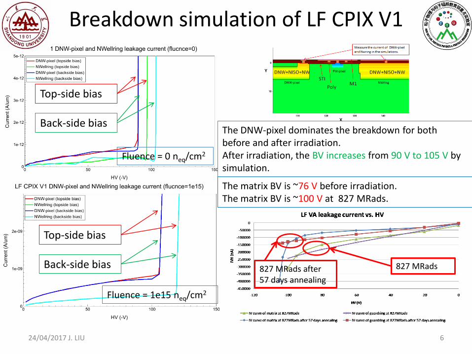
Breakdown simulation of LF CPIX V1
24/04/2017 J. LIU
The DNW-pixel dominates the breakdown for both before and after irradiation. After irradiation, the BV increases from 90 V to 105 V by simulation.
Top-side bias
Back-side bias
Top-side bias
Back-side bias
Fluence = 0 neq/cm2
Fluence = 1e15 neq/cm2
The matrix BV is ~76 V before irradiation. The matrix BV is ~100 V at 827 MRads.
827 MRads 827 MRads after 57 days annealing
6
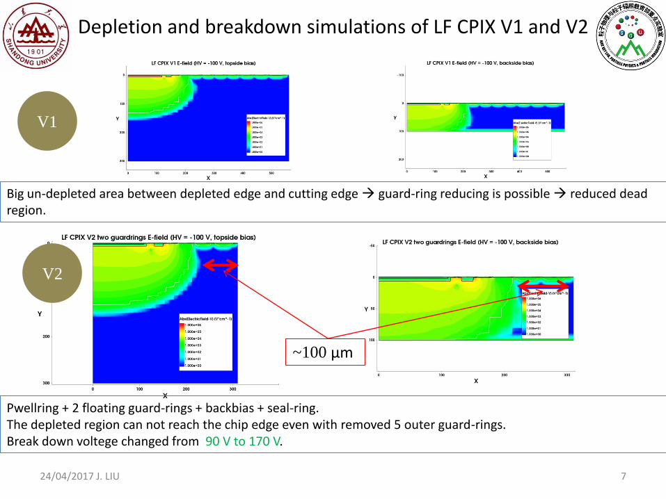
~100 µm
Depletion and breakdown simulations of LF CPIX V1 and V2
24/04/2017 J. LIU
Pwellring + 2 floating guard-rings + backbias + seal-ring. The depleted region can not reach the chip edge even with removed 5 outer guard-rings. Break down voltege changed from 90 V to 170 V.
Big un-depleted area between depleted edge and cutting edge guard-ring reducing is possible reduced dead region.
V1
V2
7
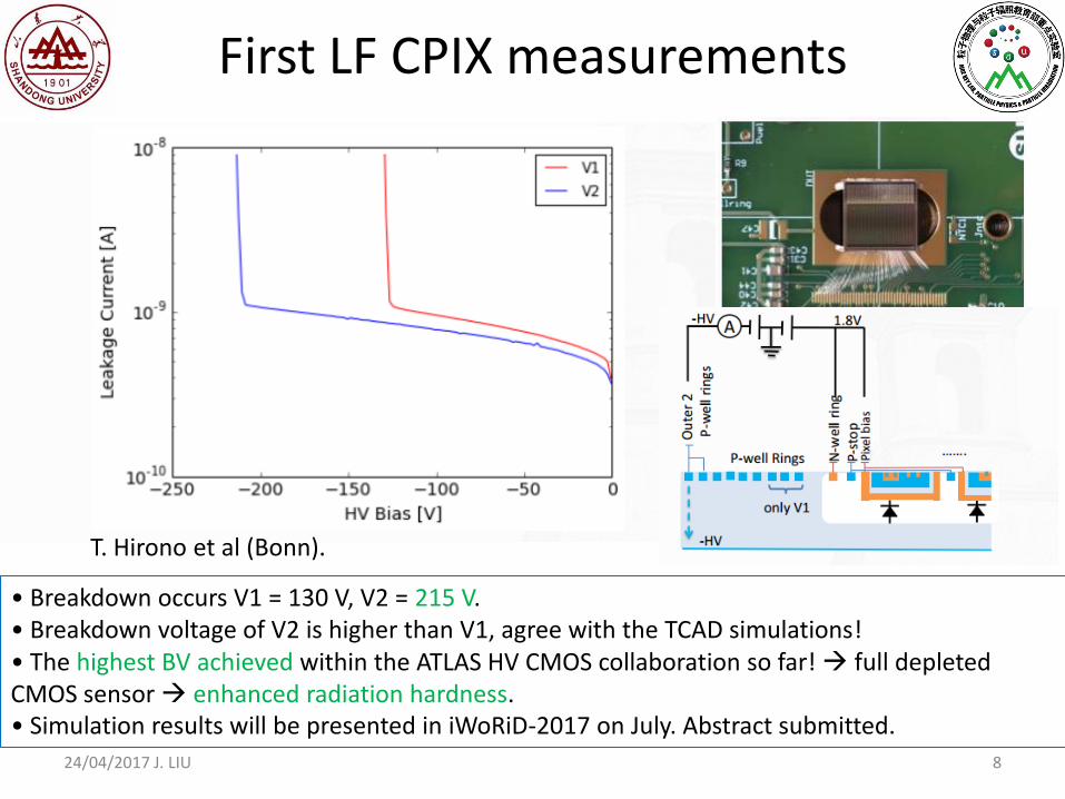
First LF CPIX measurements
24/04/2017 J. LIU 8
• Breakdown occurs V1 = 130 V, V2 = 215 V. • Breakdown voltage of V2 is higher than V1, agree with the TCAD simulations! • The highest BV achieved within the ATLAS HV CMOS collaboration so far! full depleted CMOS sensor enhanced radiation hardness. • Simulation results will be presented in iWoRiD-2017 on July. Abstract submitted.
T. Hirono et al (Bonn).
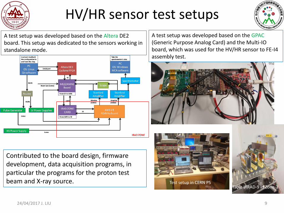
HV/HR sensor test setups
24/04/2017 J. LIU
A test setup was developed based on the Altera DE2 board. This setup was dedicated to the sensors working in standalone mode.
Table IRRAD-9 in Zone-2
Contributed to the board design, firmware development, data acquisition programs, in particular the programs for the proton test beam and X-ray source.
A test setup was developed based on the GPAC (Generic Purpose Analog Card) and the Multi-IO board, which was used for the HV/HR sensor to FE-I4 assembly test.
9
Test setup in CERN PS
LF vA LF vB
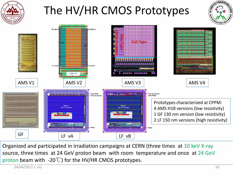
The HV/HR CMOS Prototypes
24/04/2017 J. LIU
AMS V1 AMS V4 AMS V3 AMS V2
GF
Prototypes characterized at CPPM: 4 AMS H18 versions (low resistivity) 1 GF 130 nm version (low resistivity) 2 LF 150 nm versions (high resistivity)
Organized and participated in irradiation campaigns at CERN (three times at 10 keV X-ray source, three times at 24 GeV proton beam with room temperature and once at 24 GeV proton beam with -20℃) for the HV/HR CMOS prototypes.
10
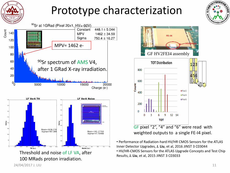
Prototype characterization
MPV= 1462 e-
24/04/2017 J. LIU
Threshold and noise of LF VA, after 100 MRads proton irradiation.
GF pixel “2”, “4” and “6” were read with weighted outputs to a single FE-I4 pixel.
GF HV2FEI4 assembly
90Sr spectrum of AMS V4, after 1 GRad X-ray irradiation.
11
• Performance of Radiation-hard HV/HR CMOS Sensors for the ATLAS Inner Detector Upgrades, J. Liu, et al, 2016 JINST 3 C03044 • HV/HR-CMOS Sensors for the ATLAS Upgrade Concepts and Test Chip Results, J. Liu, et al, 2015 JINST 3 C03033
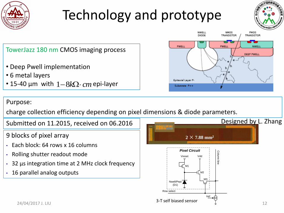
Technology and prototype
2 × 7.88 mm2
TowerJazz 180 nm CMOS imaging process • Deep Pwell implementation • 6 metal layers • 15-40 µm with epi-layer
Purpose:
charge collection efficiency depending on pixel dimensions & diode parameters.
Submitted on 11.2015, received on 06.2016
12 24/04/2017 J. LIU
cmk 81
Designed by L. Zhang
9 blocks of pixel array
• Each block: 64 rows x 16 columns
• Rolling shutter readout mode
• 32 µs integration time at 2 MHz clock frequency
• 16 parallel analog outputs
3-T self biased sensor
Row select
Co
lum
n lin
e
M3
M1
M2
Pixel Circuit
Vreset Vdd
Nwell/Pepi
(D1)
Iref
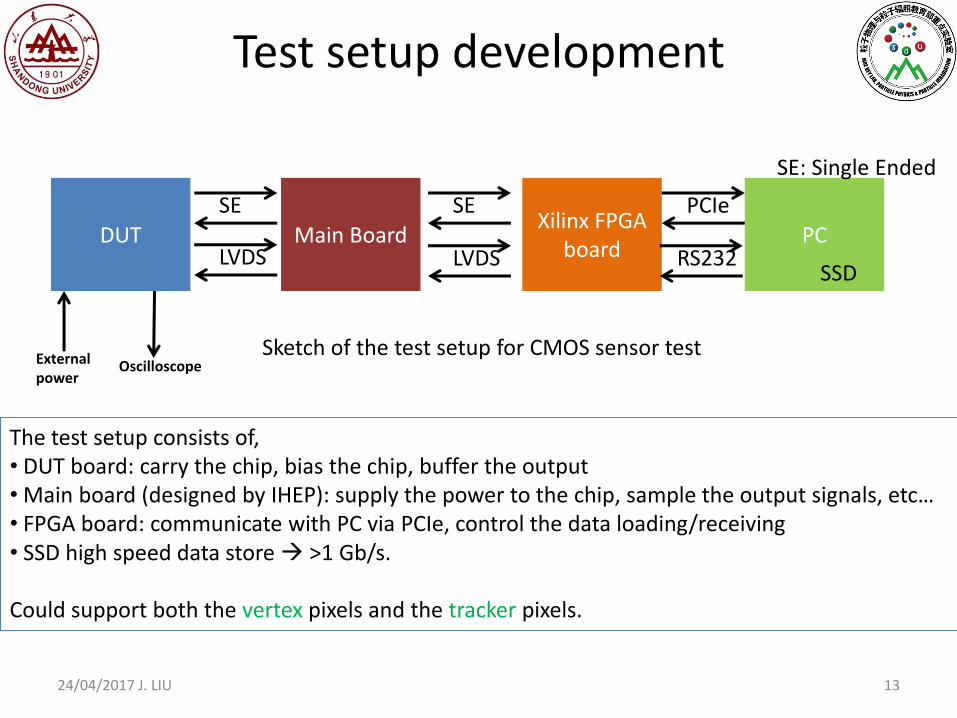
Test setup development
DUT Main Board Xilinx FPGA
board PC
SE SE
LVDS LVDS
PCIe
SE: Single Ended
Sketch of the test setup for CMOS sensor test
The test setup consists of, • DUT board: carry the chip, bias the chip, buffer the output • Main board (designed by IHEP): supply the power to the chip, sample the output signals, etc… • FPGA board: communicate with PC via PCIe, control the data loading/receiving • SSD high speed data store >1 Gb/s. Could support both the vertex pixels and the tracker pixels.
External power
Oscilloscope
13 24/04/2017 J. LIU
SSD RS232
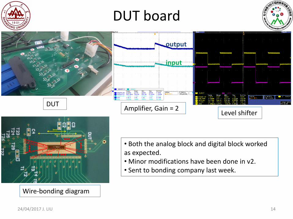
DUT board
Wire-bonding diagram
DUT
14 24/04/2017 J. LIU
• Both the analog block and digital block worked as expected. • Minor modifications have been done in v2. • Sent to bonding company last week.
Level shifter Amplifier, Gain = 2
output
input
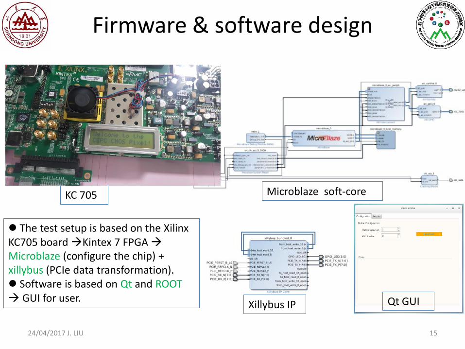
Firmware & software design
Microblaze soft-core KC 705
Qt GUI
The test setup is based on the Xilinx KC705 board Kintex 7 FPGA Microblaze (configure the chip) + xillybus (PCIe data transformation). Software is based on Qt and ROOT GUI for user.
15 24/04/2017 J. LIU
Xillybus IP
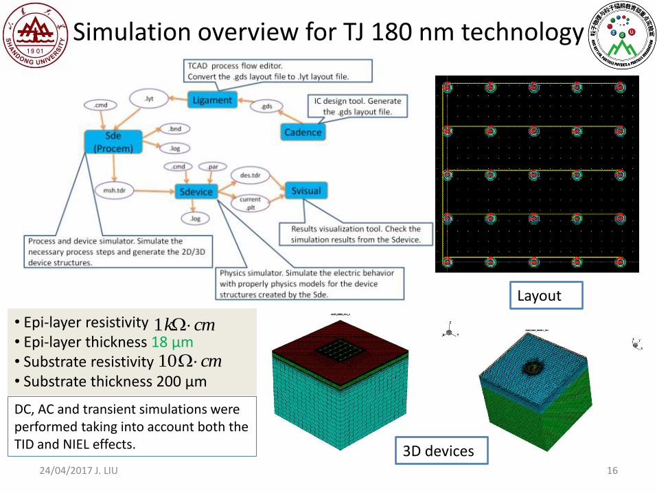
Simulation overview for TJ 180 nm technology
24/04/2017 J. LIU 16
• Epi-layer resistivity • Epi-layer thickness 18 µm • Substrate resistivity • Substrate thickness 200 µm
3D devices
Layout
DC, AC and transient simulations were performed taking into account both the TID and NIEL effects.
cmk 1
cm 10
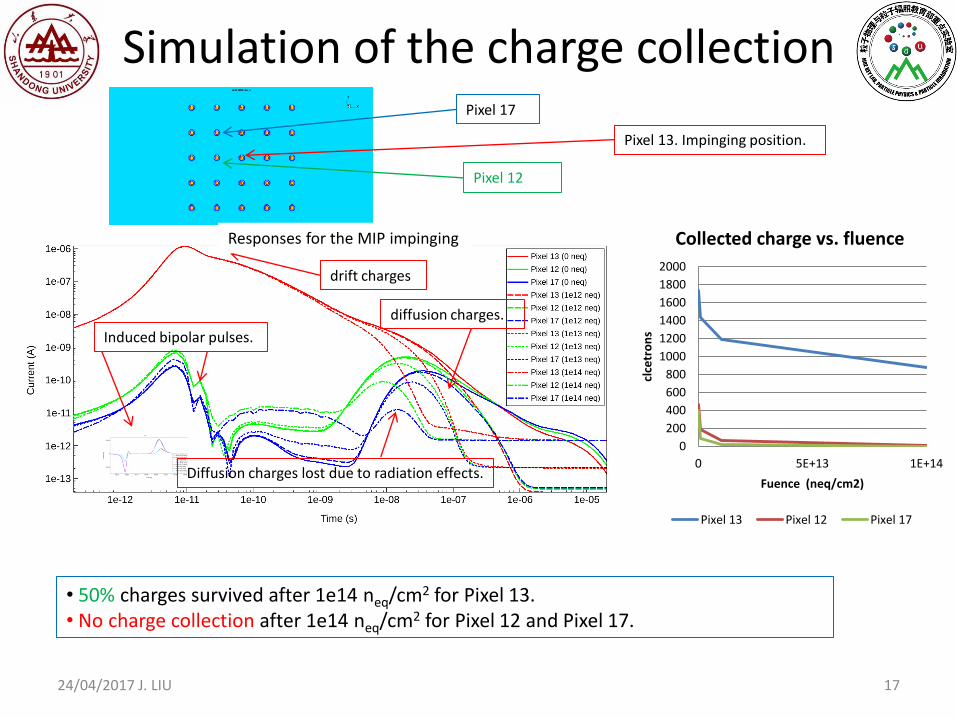
Simulation of the charge collection
17 24/04/2017 J. LIU
Pixel 13. Impinging position.
Pixel 17
drift charges
diffusion charges.
Induced bipolar pulses.
Diffusion charges lost due to radiation effects.
Responses for the MIP impinging
Pixel 12
0
200
400
600
800
1000
1200
1400
1600
1800
2000
0 5E+13 1E+14
clce
tro
ns
Fuence (neq/cm2)
Collected charge vs. fluence
Pixel 13 Pixel 12 Pixel 17
• 50% charges survived after 1e14 neq/cm2 for Pixel 13. • No charge collection after 1e14 neq/cm2 for Pixel 12 and Pixel 17.

Future plan
18 24/04/2017 J. LIU
• Finalize the CMOS sensor test setup development. Urgent needs from the CEPC sensor characterization.
• Simulate new pixel geometries w.r.t. the CEPC vertex and tracker requirements.
• Qualify the suitable HV/HR CMOS technologies for the CEPC pixels.
• Arrange the next MPW run by using a 350 nm HV/HR BCD process, which is dedicated to the pixelated CEPC tracker and radiation damage study.
• Parameterize the TID and the NIEL effects for the corresponding CMOS sensors.
Conclusion and perspectives • ATLAS:
– Seven prototypes have been characterized. Radiation harness to 100 MRads and 1015 neqcm-2 an option for the HL-LHC. TDR by the end of 2017.
– The first HV/HR CMOS demonstrator by using the LF 150 nm technology has been designed and is under characterization.
– The TCAD simulations of the CMOS sensors show good agreement with the measurements.
– Expected improvements have been observed from the preliminary tests.
• CEPC:
– A test setup based on Xilinx Kintex-7 FPGA is under developing. Could support both the vertex and tracker pixels.
– TCAD simulations for the TJ 180 nm technology have been performed. Both the DC, AC and transient properties were explored. The current sensor layout might not work for the CEPC vertex detector.
– The PCBs have been designed and are under testing. The firmware and software developments are in process. First data taking will be in summer.
– New pixel geometries for both the vertex and tracker cases will be simulated carefully try to achieve >99% fill factor after 1e14 neq/cm2.
– HV/HR technology investigation is ongoing for the CEPC vertex and tracker.
– Preparing the next MPW run for the CEPC pixelated silicon tracker.
19 24/04/2017 J. LIU

Conclusion and perspectives • ATLAS:
– Seven prototypes have been characterized. Radiation harness to 100 MRads and 1015 neqcm-2 an option for the HL-LHC. TDR by the end of 2017.
– The first HV/HR CMOS demonstrator by using the LF 150 nm technology has been designed and is under characterization.
– The TCAD simulations of the CMOS sensors show good agreement with the measurements.
– Expected improvements have been observed from the preliminary tests.
• CEPC:
– A test setup based on Xilinx Kintex-7 FPGA is under developing. Could support both the vertex and tracker pixels.
– TCAD simulations for the TJ 180 nm technology have been performed. Both the DC, AC and transient properties were explored. The current sensor layout might not work for the CEPC vertex detector.
– The PCBs have been designed and are under testing. The firmware and software developments are in process. First data taking will be in summer.
– New pixel geometries for both the vertex and tracker cases will be simulated carefully try to achieve >99% fill factor after 1e14 neq/cm2.
– HV/HR technology investigation is ongoing for the CEPC vertex and tracker.
– Preparing the next MPW run for the CEPC pixelated silicon tracker.
20 24/04/2017 J. LIU


![RENORMALONS IN INCLUSIVE DECAY ηQ - Indico [Home]indico.ihep.ac.cn/event/6822/session/7/contribution/31/material/... · Effect of resummation cancels for gluons in the initial state,](https://img.pdfslide.tips/doc/110x75/5af37dc77f8b9a9e598b5ab7/renormalons-in-inclusive-decay-q-indico-home-of-resummation-cancels-for-gluons.jpg)