Embed Size (px)
Citation preview
1
Supplementary Information for:
Direct observation of the energetics at a semiconductor/liquid junction by operando X-ray photoelectron spectroscopy
Michael F. Lichtermana,b*, Shu Hua,b*, Matthias H. Richterb*, Ethan J. Crumlinc*,
Stephanus Axnandac, Marco Favarob,c, Walter Drisdellb,c, Zahid Hussainc, Thomas Mayerd,
Bruce S. Brunschwigb,e‡, Nathan S. Lewisa,b,f‡, Zhi Liuc,g,h‡, and Hans-Joachim Lewerenzb‡
a Division of Chemistry and Chemical Engineering, California Institute of Technology, Pasadena,
CA 91125, USA.
b Joint Center for Artificial Photosynthesis, California Institute of Technology, Pasadena,
CA 91125, USA.
c Advanced Light Source, Lawrence Berkeley National Laboratory, Berkeley, CA 94720
d Surface Science Division, Materials Science Department, Darmstadt University of Technology,
64287 Darmstadt, Germany.
e Beckman Institute, California Institute of Technology, Pasadena, CA 91125, USA
f Kavli Nanoscience Institute, California Institute of Technology, Pasadena, CA 91125, USA.
g State Key Laboratory of Functional Materials for Informatics, Shanghai Institute of
Microsystem and Information Technology, Chinese Academy of Sciences, Shanghai 200050,
People’s Republic of China
h School of Physical Science and Technology, ShanghaiTech University, Shanghai 200031,
China
* These authors contributed equally to the work. MFL, SH and MHR contributed to the design, execution, and analysis of the experiment; EJC was critical in the design, building and testing of the end station that allows atmospheric pressure XPS data collection on a solution under potentiostatic control.
‡ Corresponding authors: E-mail: [email protected], [email protected], [email protected], [email protected]
Electronic Supplementary Material (ESI) for Energy & Environmental Science.This journal is © The Royal Society of Chemistry 2015
2
Electrolyte Choice
At room temperature and pressure, water requires 1.23 V, plus catalytic overpotentials to
produce 1 atm of hydrogen and oxygen gas. The overpotential at ~ 10 mA⋅cm-2 for the OER is
~ 200–300 mV and is for the HER ~ 5–200 mV with a good catalyst. Thus the electrochemical
window for water splitting is ~ 1.4 V to 1.7 V. The potential window is still further increased for
a poor catalyst and/or a substantial resistive element in the cell. For example, as TiO2 is a poor
OER catalyst, the usable potential range is substantially increased. While a lower pressure of
oxygen and/or hydrogen will slightly lower (by ~ 100 mV) the potential required, the potential
window is substantially larger than 1.23 V.
Although aqueous KOH is highly corrosive, the Pourbaix diagram for titanium has a
large region in which TiO2 thermodynamically (and also kinetically) is the stable phase over a
pH region from 0 to 14 and a potential range that spans the limits of water splitting (and beyond).
Thus, a TiO2 electrode is stable in contact with 1 M KOH at the potentials used here. Under an
oxidizing potential the nickel will convert to a nickel oxide, NiOx, which is also Pourbaix stable
in 1 M KOH.
Experimental
Electrodes of TiO2, deposited by ALD as has been described recently 1, were prepared on
degenerately boron-doped p-type silicon (“p+-Si”) substrates. Silicon wafers were cleaned with
RCA SC-1 by soaking in a 3:1 (by volume) solution of concentrated H2SO4 to 30 % H2O2 for
2 min before etching for 10 s in a 10 % (by volume) solution of hydrofluoric acid. The wafers
were then etched with RCA SC-2 procedure of soaking in a 5:1:1 (by volume) solution of H2O,
36 % hydrochloric acid, and 30 % hydrogen peroxide for 10 min at 75 °C. Directly after the
cleaning procedure, TiO2 was deposited by ALD from a tetrakis(dimethylamido)titanium
3
(TDMAT) precursor. A 0.1 s pulse of TDMAT was followed by 15 s purge of N2 at 20 sccm,
following by a 0.015 s pulse of H2O before another 15 s purge with N2. This process was
repeated for 1500 cycles. Samples requiring Ni were loaded into a RF sputtering system. Ni was
deposited at a RF sputtering power of 150 W for 20 s to 60 s. Atomic-force microscopy (AFM)
images (Fig. S8) attested to the smoothness of these films.
To prepare electrodes for operando XPS investigation, strips of the p+-Si/TiO2/(Ni)
wafers were cut to 1 cm x 3.5 cm. An In/Ga eutectic was scribed into the back of the Si wafer,
followed by Ag paint. The electrode was then was contacted by a strip of Cu tape supported on a
0.8 cm x 3 cm glass slide. The entire assembly was enclosed with non-conductive epoxy
(Hysol 9460) to ensure that there no contact of the In/Ga, silver paint, copper tape, or Si
electrode back and edges by the electrolyte during the AP-XPS measurements.
To perform the operando AP-XPS measurements, the p+-Si/TiO2/(Ni) electrode was
mounted and contacted by a three-axis manipulator onto which the Ag/AgCl reference electrode
(eDAQ) and a platinum foil counter electrode were also mounted and separately contacted
(Fig. S2). The manipulator movements were computer controlled, allowing for manipulation of
the sample position and the optimization of data collection, with a spatial resolution of ±10 µm.
A PEC-beaker positioned below the three-electrode setup was filled with the electrolyte (1.0 M
KOH) and raised or lowered as necessary, and was generally held as close to the XPS sampling
cone as possible. To maintain the water-vapor pressure and to prevent the rapid evaporation of
water from the PEC-beaker, a second, larger beaker, filled with sacrificial 18.2 MΩ cm
resistivity water, was positioned next to the PEC-beaker (see Fig. S2). The working, reference,
and counter electrode clips from a Biologic SP-300 potentiostat were connected to their
respective external connection clips on the stage. The working electrode was also grounded to
4
the detector of the UHV surface analysis system, to equalize the Fermi energy of the detector
with the back contact of the working electrode.
To collect data, the sample was “dipped” into the electrolyte before a potential was set.
The electrode was then raised to such a height that a thin film of the electrolyte (~ 13 nm) was
present at the XPS sampling location. The signal at the detector was maximized by manipulation
of the sample position, and locations were chosen at which both the H2O and TiO2 signals were
clearly resolved in the O 1s core level during snapshot mode operation of the detector. This
process ensured sufficient electrolyte coverage, necessary for the control of electric potential,
while allowing for the collection of data from the underlying electrode.
AP-XPS data were collected on a Scienta R4000 HiPP-2 system in which the
photoelectron collection cone was aligned to the beamline X-ray spot at a distance of ~ 300 µm 2.
The system used differential pumping supplied by four turbo pumps, backed by liquid-nitrogen
trap protected rough pumps, to maintain a pressure of ~ 5 x 10⁻⁷ mbar at the detector while
allowing a stable pressure of 20-27 mbar at the sampling position. The pressure range used
herein was bounded by an upper limit due to photoelectron collection efficiency and the pumping
speed of the differential pumping system and by a lower limit given by the boiling point of
water. Higher vapor pressures lead to significantly longer data collection times and a decrease in
the signal to noise ratio. Beamline 9.3.1 at the Advanced Light Source was used to provide
Tender X-rays at 4 keV of energy out of a possible photon energy range of 2.3-5.2 keV with a
resolving power of E/ΔE = 3000-7200. Photoelectrons for Ti 2p, O 1s, and Ni 2p levels were
therefore collected in kinetic energy ranges of 3538±8 eV, 3466±8 eV, and 3142±8 eV,
respectively.
5
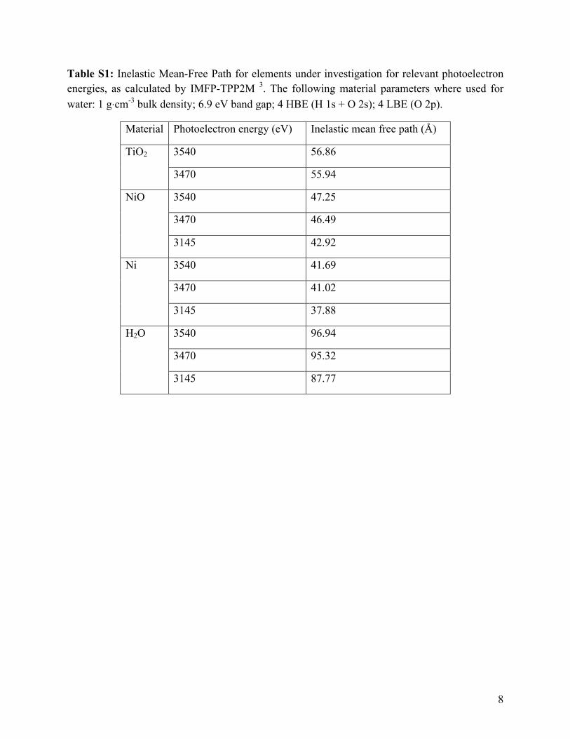
Table S1 lists the inelastic mean-free paths (IMFPs) through titania and water for
photoelectrons at the above kinetic energies 3. One critical aspect of this experiment is the
significantly higher IMFP of photoelectrons through the water than through the titania, which
effectively determines that the titania, and not the thickness of the water overlayer above it, will
be the primary determinant affecting the sampling depth of the XPS experiment within the
electrode. As the inelastic mean free path of a photoelectron that originates in the TiO2 or Nickel
/Nickel Oxide is substantially higher in water than in the solid, the effect of small variations in
electrolyte layer thickness is small. The numbers provided for IMFP through water are likely
somewhat underestimated due to the model used by the TPP2M calculation, as a recent
publication suggests 4.
Consecutive iterative scans of the O 1s, Ti 2p, and Ni 2p core levels were performed
individually at potentials between -1.4 V and +0.6 V vs. the Ag/AgCl reference. Potentials
outside of this range (under HER or OER conditions) resulted in a dried out electrolyte layer,
resulting in a loss of potential control; a thicker electrolyte layer, resulting in a loss of
observation of data from the underlying electrode; or caused bubbles, which disrupted or
destroyed the conductive electrolyte film and risked damaging the detector. After collection, the
consecutive scans were averaged. The data presented herein were obtained from the summed
data. Generally, relatively few scans (~ 7) were needed for the O 1s spectra, whereas more scans
were needed for robust detection and analysis of the Ti 2p (~ 21) signal. The Ni data required
hours (> 50 sweeps) to produce spectra with an acceptable signal-to-noise ratio. All of the
AP-XPS data were fitted with CasaXPS and IgorPro.
Differential capacitance vs. potential data was recorded on SP-200 and SP-300 Bio-Logic
potentiostats equipped with impedance spectroscopy. The impedance vs. potential data was fitted
6
with Zfit to obtain the desired differential capacitance vs. potential data. A Randles circuit,
which contains a resistor in series with a parallel resistor and capacitor as shown below, was
used as the equivalent circuit model for the impedance data.
Charging and Extra Atomic Relaxation
In addition to the applied potential, a screening and surface charging effect could also
affect the position of core levels, through extra atomic relaxation and surface charging of a
compact oxide layer. For a structure in contact with solution, the latter can be neglected as
photogenerated surface charges are neutralized. The former can be considered constant for a
single compound and electrode geometry, as described in 5. We can therefore discuss the
findings in terms of energy-band relations.
Band Bending analysis and calculation
A narrow AP-XPS peak is expected near the flat-band potential (the Fermi level is 0.2 eV
below the CB, see Fig. S7; the band gap for TiO2 is 3.34 eV 1) whereas a wider peak is expected
at other applied potentials. This effect is due to integral nature of the summation of the core
signals, and is observed provided that the space-charge region is of a size comparable to the
escape depth, λ, of the created photoelectrons, i.e. 0.1 < dSCR/3λ < 10. Considering a doping
concentration of ~ 2 x 1019 cm-3, as obtained from Mott-Schottky analysis for εr = 85 (Fig. 5b),
7
and a potential of U = 1.0 V the width of the space charge region is in the order of the escape
depth for Ti 2p with λ = 56.86 Å, i.e. dSCR = 30 nm and dSCR/3λ = 1.8.
For such systems, equation (S1) describes the numerical evaluation of the core level
emission line profile as a function of applied potential U, with the relative contribution of each
subsequent band-bending depth layer to the overall XPS peak intensity. PF is the peak function
of the corresponding core level (e.g. a Voigt profile), d is the sample thickness and 𝜉 𝑥,𝑈 is the
electrostatic potential as obtained by solving the Poisson equation using Fermi-Dirac statistics
instead of the more simple Boltzmann statistics. The potential behavior of the core level
emission line profile is then described by:
I 𝑈 = e!!
! ∙ PF ξ x,𝑈 ∂x!! (S1).
Figure S11 depicts the numerical simulation of a core level under an increasingly positive
potential. In conjunction with an expected core level shift to lower binding energies, a peak
broadening on the higher binding-energy part of the core level is predicted for positive
potentials, resulting in an asymmetric peak shape. From such results, extraction of the flat-band
potential (Ufb) of the semiconductor can be performed without the use of Mott-Schottky 6
analysis. Specifically, the flat-band potential should coincide with the minimum of the FWHM,
e.g. UBB(x) = 0.
Additionally, an asymmetry in the Ti signal is expected, due to limited sampling of the
dropping (for U > Ufb) or rising (U < Ufb) region of band bending associated with the integral
exponential dependence of the core level intensity from the information depth (see Fig. S11). As
can be seen from the relative contributions of the left (higher binding energy) and right (lower
binding energy) sides of the peak, this asymmetry was observed experimentally, and agrees well
with the Mott-Schottky data.
8
Table S1: Inelastic Mean-Free Path for elements under investigation for relevant photoelectron energies, as calculated by IMFP-TPP2M 3. The following material parameters where used for water: 1 g⋅cm-3 bulk density; 6.9 eV band gap; 4 HBE (H 1s + O 2s); 4 LBE (O 2p).
Material Photoelectron energy (eV) Inelastic mean free path (Å)
TiO2 3540 56.86
3470 55.94
NiO 3540 47.25
3470 46.49
3145 42.92
Ni 3540 41.69
3470 41.02
3145 37.88
H2O 3540 96.94
3470 95.32
3145 87.77
9
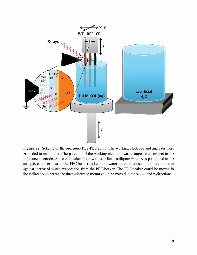
Figure S2: Scheme of the operando PES-PEC setup. The working electrode and analyzer were grounded to each other. The potential of the working electrode was changed with respect to the reference electrode. A second beaker filled with sacrificial millipore water was positioned in the analysis chamber next to the PEC-beaker to keep the water pressure constant and to counteract against increased water evaporation from the PEC-beaker. The PEC-beaker could be moved in the z-direction whereas the three-electrode mount could be moved in the x-, y-, and z-directions.
��
� ���
�"�
��� ��� ���
�"�����
���
��� ����"�
�'����!��'�
����
&!%�����#��$�
��
��
������������'�
��
�����
'�
10
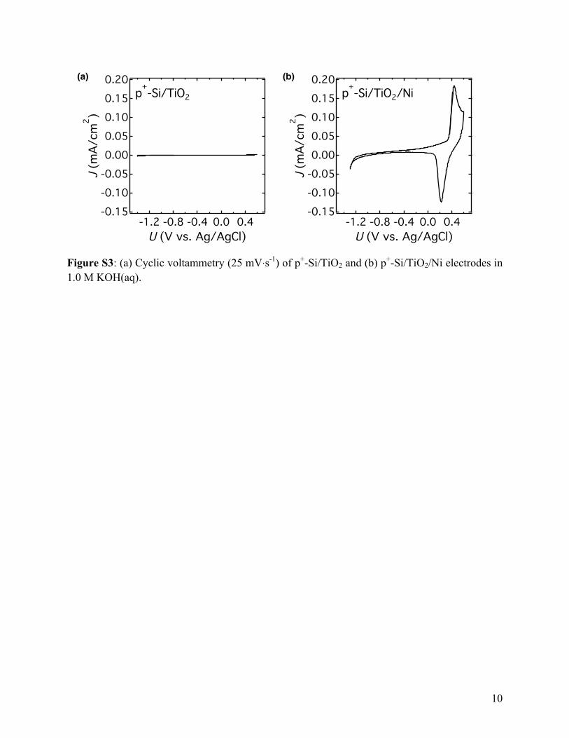
Figure S3: (a) Cyclic voltammetry (25 mV⋅s-1) of p+-Si/TiO2 and (b) p+-Si/TiO2/Ni electrodes in 1.0 M KOH(aq).
(a)� (b)�
11
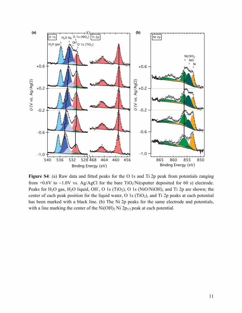
Figure S4: (a) Raw data and fitted peaks for the O 1s and Ti 2p peak from potentials ranging from +0.6V to −1.0V vs. Ag/AgCl for the bare TiO2/Ni(sputter deposited for 60 s) electrode. Peaks for H2O gas, H2O liquid, OH-, O 1s (TiO2), O 1s (NiO/NiOH), and Ti 2p are shown; the center of each peak position for the liquid water, O 1s (TiO2), and Ti 2p peaks at each potential has been marked with a black line. (b) The Ni 2p peaks for the same electrode and potentials, with a line marking the center of the Ni(OH)2 Ni 2p3/2 peak at each potential.
+0.6
+0.2
-0.2
-0.6
-1.0
U (V
vs.
Ag/
AgCl
)
865 860 855 850Binding Energy (eV)
Ni 2p
Ni(OH)2NiO
Ni+0.6
+0.2
-0.2
-0.6
-1.0
U (V
vs.
Ag/
AgCl
)
540 536 532 528Binding Energy (eV)
468 464 460 456
O 1s Ti 2p H2O liq. OH-
H2O gas O 1s (TiO2)
O 1s (NiOx)(a)� (b)�
12
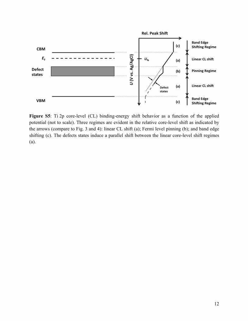
Figure S5: Ti 2p core-level (CL) binding-energy shift behavior as a function of the applied potential (not to scale). Three regimes are evident in the relative core-level shift as indicated by the arrows (compare to Fig. 3 and 4): linear CL shift (a); Fermi level pinning (b); and band edge shifting (c). The defects states induce a parallel shift between the linear core-level shift regimes (a).
��
���
���
��������������
���������������
���!����������
���������������
��������������
�������������������������
�������������������������
#�$�
#�$�
#�$�
#�$�
#�$�
���
��#
� �!���"��
��$�
��������������
13
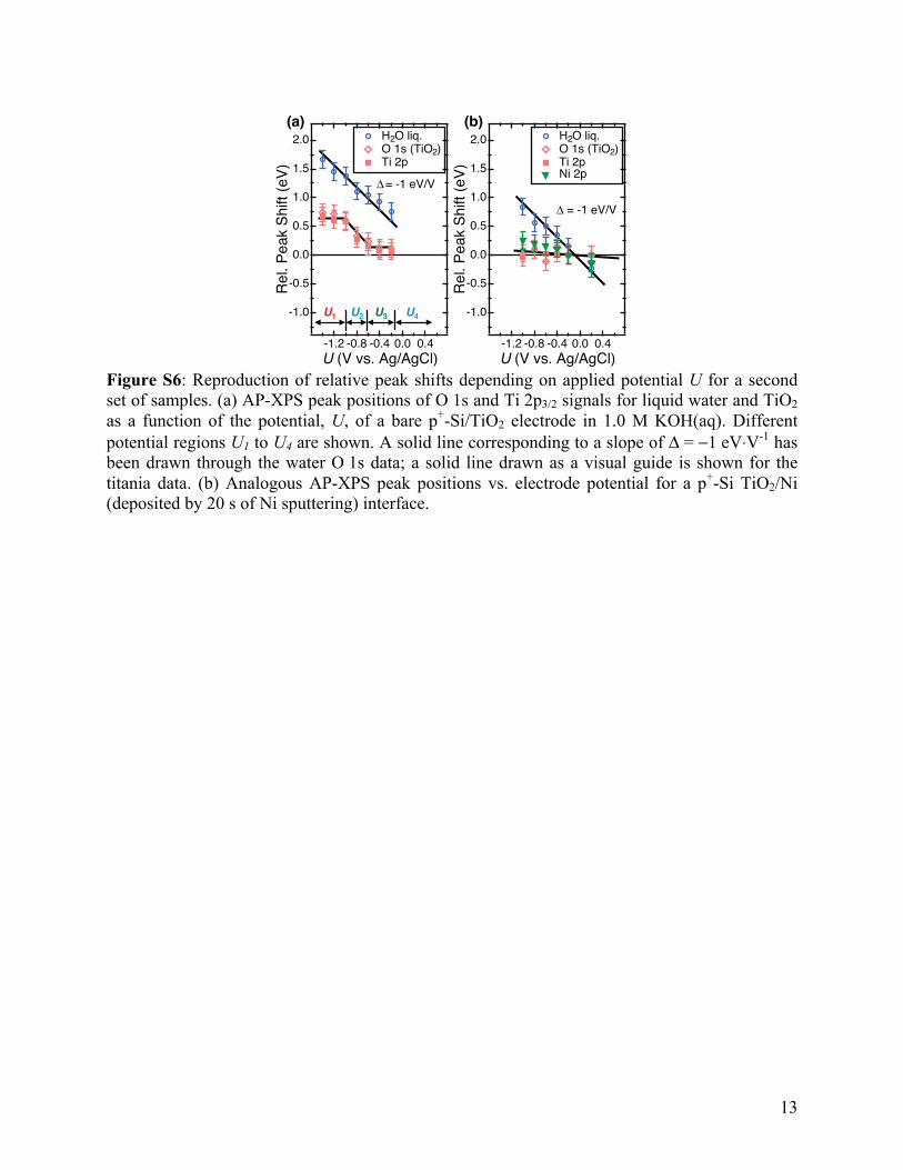
Figure S6: Reproduction of relative peak shifts depending on applied potential U for a second set of samples. (a) AP-XPS peak positions of O 1s and Ti 2p3/2 signals for liquid water and TiO2 as a function of the potential, U, of a bare p+-Si/TiO2 electrode in 1.0 M KOH(aq). Different potential regions U1 to U4 are shown. A solid line corresponding to a slope of Δ = −1 eV⋅V-1 has been drawn through the water O 1s data; a solid line drawn as a visual guide is shown for the titania data. (b) Analogous AP-XPS peak positions vs. electrode potential for a p+-Si TiO2/Ni (deposited by 20 s of Ni sputtering) interface.
2.0
1.5
1.0
0.5
0.0
-0.5
-1.0
Rel.
Peak
Shi
ft (e
V)
-1.2 -0.8 -0.4 0.0 0.4U (V vs. Ag/AgCl)
� = -1 eV/V
H2O liq. O 1s (TiO2) Ti 2p
2.0
1.5
1.0
0.5
0.0
-0.5
-1.0
Rel.
Peak
Shi
ft (e
V)
-1.2 -0.8 -0.4 0.0 0.4U (V vs. Ag/AgCl)
H2O liq. O 1s (TiO2) Ti 2p Ni 2p
� = -1 eV/V
(a)� (b)�
U3�U2�U1� U4�
14
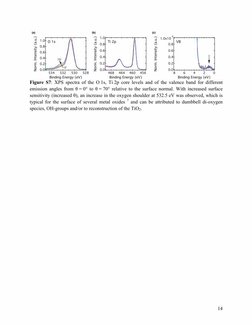
Figure S7: XPS spectra of the O 1s, Ti 2p core levels and of the valence band for different emission angles from θ = 0° to θ = 70° relative to the surface normal. With increased surface sensitivity (increased θ), an increase in the oxygen shoulder at 532.5 eV was observed, which is typical for the surface of several metal oxides 7 and can be attributed to dumbbell di-oxygen species, OH-groups and/or to reconstruction of the TiO2.
(a)� (b)� (c)�
15
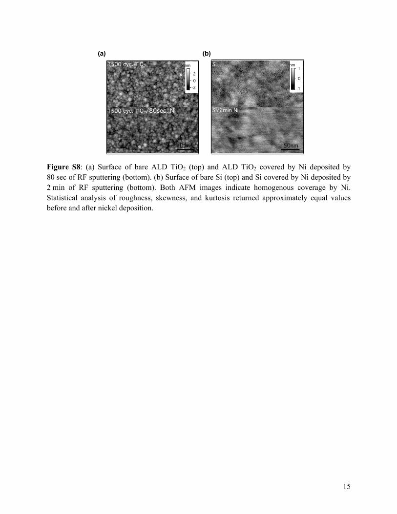
Figure S8: (a) Surface of bare ALD TiO2 (top) and ALD TiO2 covered by Ni deposited by 80 sec of RF sputtering (bottom). (b) Surface of bare Si (top) and Si covered by Ni deposited by 2 min of RF sputtering (bottom). Both AFM images indicate homogenous coverage by Ni. Statistical analysis of roughness, skewness, and kurtosis returned approximately equal values before and after nickel deposition.
(a)� (b)�
16
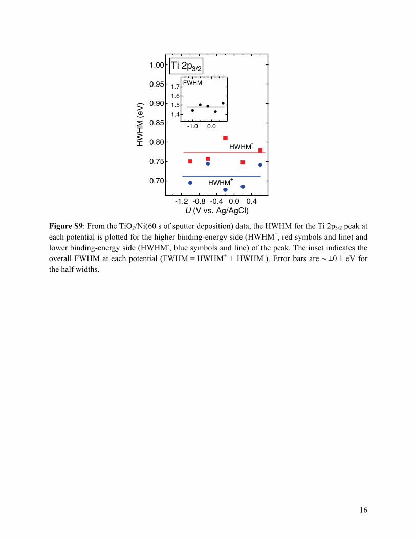
Figure S9: From the TiO2/Ni(60 s of sputter deposition) data, the HWHM for the Ti 2p3/2 peak at each potential is plotted for the higher binding-energy side (HWHM+, red symbols and line) and lower binding-energy side (HWHM-, blue symbols and line) of the peak. The inset indicates the overall FWHM at each potential (FWHM = HWHM+ + HWHM-). Error bars are ~ ±0.1 eV for the half widths.
1.00
0.95
0.90
0.85
0.80
0.75
0.70
HW
HM
(eV)
-1.2 -0.8 -0.4 0.0 0.4U (V vs. Ag/AgCl)
HWHM-
HWHM+
Ti 2p3/2
1.71.61.51.4
-1.0 0.0
FWHM
17
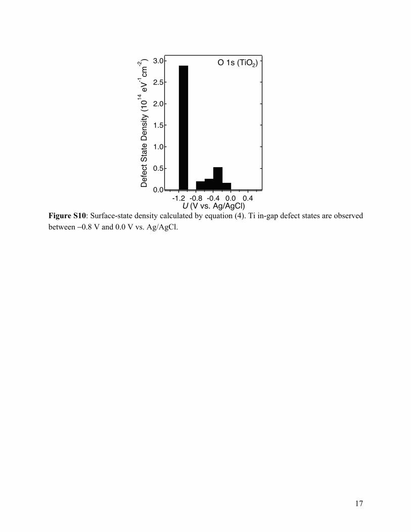
Figure S10: Surface-state density calculated by equation (4). Ti in-gap defect states are observed between −0.8 V and 0.0 V vs. Ag/AgCl.
3.0
2.5
2.0
1.5
1.0
0.5
0.0Defe
ct S
tate
Den
sity
(1014
eV-1
cm-2
)
-1.2 -0.8 -0.4 0.0 0.4U (V vs. Ag/AgCl)
O 1s (TiO2)
18
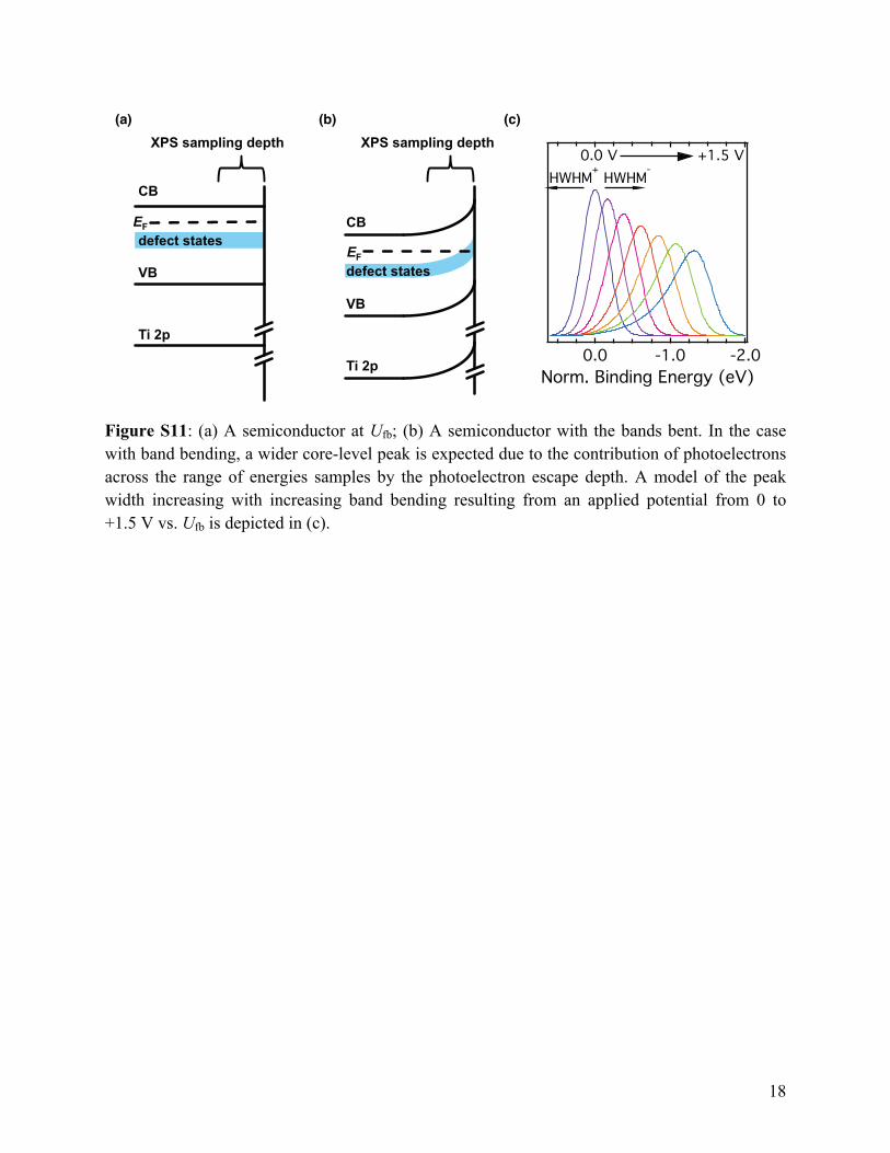
Figure S11: (a) A semiconductor at Ufb; (b) A semiconductor with the bands bent. In the case with band bending, a wider core-level peak is expected due to the contribution of photoelectrons across the range of energies samples by the photoelectron escape depth. A model of the peak width increasing with increasing band bending resulting from an applied potential from 0 to +1.5 V vs. Ufb is depicted in (c).
(a)� (b)� (c)�
CB
VB
Ti 2p
EF defect states
XPS sampling depth
CB
VB
Ti 2p
defect states
XPS sampling depth
EF
19
References
1. S. Hu, M. R. Shaner, J. A. Beardslee, M. F. Lichterman, B. S. Brunschwig, and N. S. Lewis, Science, 2014, 344, 1005–1009.
2. S. Axnanda, E. J. Crumlin, B. Mao, S. Rani, R. Chang, P. G. Karlsson, M. O. M. Edwards, M. Lundqvist, R. Moberg, P. Ross, Z. Hussain, and Z. Liu, Sci. Rep., 2015, 5, 9788.
3. QUASES-IMFP-TPP2M Inelastic electron mean free path calculated from the Tanuma, Powell, and Penn TPP2M formula in S. Tanuma, C. J. Powell, and D. R. Penn, Surf. Interface Anal., 1994, 21, 165–176. Code written by Sven Tougaard. Copyright (c) 2000-2010 Quases-Tougaard Inc. Free to use for non-commercial applications.
4. N. Ottosson, M. Faubel, S. E. Bradforth, P. Jungwirth, and B. Winter, J. Electron Spectrosc., 2010, 177, 60–70.
5. S. Kohiki, Spectrochim Acta B, 1999, 54, 123–131. 6. F. Fabregat-Santiago, G. Garcia-Belmonte, J. Bisquert, P. Bogdanoff, and A. Zaban, J.
Electrochem. Soc., 2003, 150, E293–E298. 7. J. Haeberle, M. H. Richter, Z. Galazka, C. Janowitz, and D. Schmeißer, Thin Solid Films,
2014, 555, 53–56.


![Direct observation of protein residue solvation dynamicsbose.res.in/~skpal/papers/CHT_solvation_JPPA.pdfspecific sites of proteins and nucleic acids [1]. Especially, the specific](https://img.pdfslide.tips/doc/110x75/5f4917d3d6cf557fdf7d8a69/direct-observation-of-protein-residue-solvation-skpalpaperschtsolvationjppapdf.jpg)


![[Supplementary materials]](https://img.pdfslide.tips/doc/110x75/56816583550346895dd82b8a/supplementary-materials-56cd0e37cc26b.jpg)