Embed Size (px)
Citation preview
1
Zero-Order view of PLL (and role of VCO)
ν-to-φ∗
VCO2
νi φi
φosc
Key Objective of Phase-Locked Loop:Use the “phase comparator” block (X) to keep “red” VCO doing exactly what the incoming signal is doing. This can either: a) guarantee “clock synchronization” or
b) “demodulate” FM signals (initially coming from “green”).
νoVCO1νi
Input: voice signals…
Output: FM-modulated signals…
νo
“a”
“f”
*A word about units:Phase is the working units in the “feedback equations”…
Transfer Function--vo/φiA=a/[1+af]
This slide and the next one are intended give conceptual (intuitive?) views of how the PLL works. The words may actually be very similar between the two slides.VCO=FM Modulation (Lab 2)Multiplier (=“X”)…(Lab 1)Feedback (A=a/[1+af])…(Lab 3…different target application)
Putting them together, with a slightly strange twist, we can create the Phase-Locked Loop (PLL)That is, IF (you may have to read a lot more to totally understand this in detail…) we can achieve a feedback function such that A~1/f then the vo that drives that feedback function IS the original modulating signalA key (again, that will require work in terms of reading and digesting the derivation etc.) is to understand that the UNITS of feedback…and to use them properly
The Phase-Locked Loop (PLL)
2
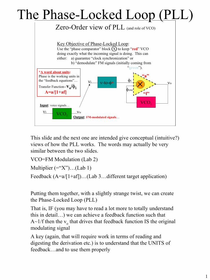
The Analogy between O/A feedback and PLL
νi
νo
iin ifb
Virtual groundRequires that:iin = - ifb
ν-to-φ
VCO2
νi φi
φosc
νo
R1 R2
νo=VCO1νi
This is a very (overly) simple view of how the PLL might be thought of in the context of a feedback loop.That is, for the inverting O/A the summing node (into the O/A) results in the driven node at the output to have a voltage such that the currents match at the input.For the PLL the “X” (phase comparator) block takes the two FM signals--one from our modulating source, the other created by the VCO within the PLL--and creates a output Vo such that the two incoming signals exactly match each other (frequency and a well-defined phase relationship)If this seems too simplistic, that’s OK… the following math and details provided by text information from Mayaram and Grebene should flesh out the story.The key points include: a) this is a feedback problem and b) thefeedback function basically generates [VCO]-1--the inverse of what is coming into the system which was used to encode the information (via the VCO block on the transmitter side)
3
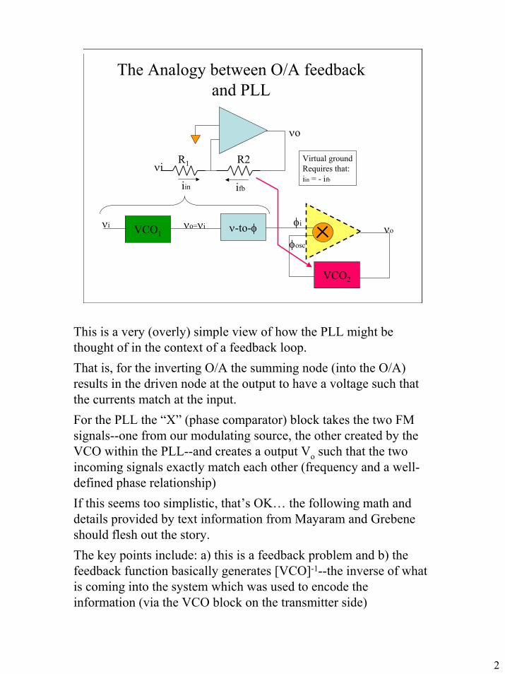
(Grebene)
This is the first of the figures (from Alan Grebene’s book…same one I used in explaining the 566) that give details about both the internal components of the PLL and the external behavior of PLL performance.TOP figure--this is the same block diagram as the previous slides but now adds “loop filter” and “amplifier”. The loop filter is a BIG DEAL. It (and the amplifier) is needed to “condition” the signal in order for it to NOT “confuse” the VCO (TBD).BOTTOM figure--this adds some terminology about KD, F(s), A, KO and, maybe most importantly, the “1/s” term. As we will see, this is the step that in fact gets us to “φ ” as the feedback variable.The next few slides show how the “error signal” (=Ve(t)) looks in time, what the meaning of the “ranges” of capture and hold for the PLL getting/staying “in LOCK” (as in Phase-LOCKED)
4
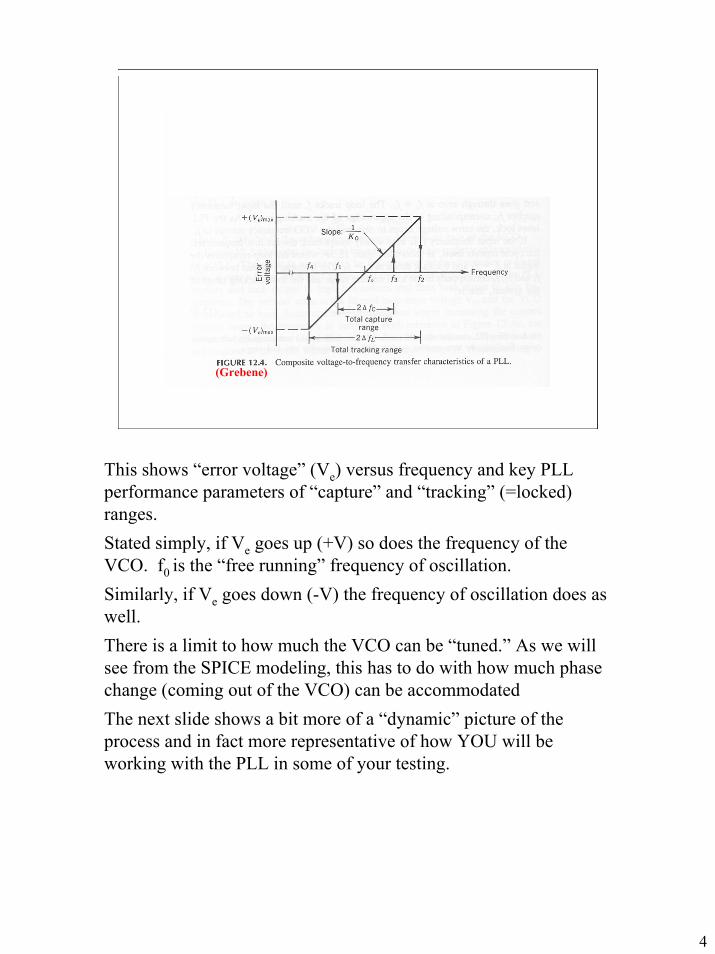
(Grebene)
This shows “error voltage” (Ve) versus frequency and key PLL performance parameters of “capture” and “tracking” (=locked) ranges.Stated simply, if Ve goes up (+V) so does the frequency of the VCO. f0 is the “free running” frequency of oscillation.Similarly, if Ve goes down (-V) the frequency of oscillation does as well.There is a limit to how much the VCO can be “tuned.” As we will see from the SPICE modeling, this has to do with how much phase change (coming out of the VCO) can be accommodatedThe next slide shows a bit more of a “dynamic” picture of the process and in fact more representative of how YOU will be working with the PLL in some of your testing.
5
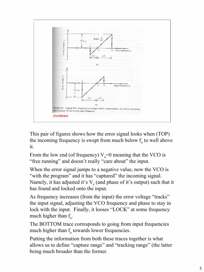
(Grebene)
This pair of figures shows how the error signal looks when (TOP)the incoming frequency is swept from much below fo to well above it.From the low end (of frequency) Ve=0 meaning that the VCO is “free running” and doesn’t really “care about” the input.When the error signal jumps to a negative value, now the VCO is “with the program” and it has “captured” the incoming signal. Namely, it has adjusted it’s Ve (and phase of it’s output) such that it has found and locked onto the input.As frequency increases (from the input) the error voltage “tracks” the input signal, adjusting the VCO frequency and phase to stay in lock with the input. Finally, it looses “LOCK” at some frequency much higher than fo.The BOTTOM trace corresponds to going from input frequencies much higher than fo towards lower frequencies.Putting the information from both these traces together is what allows us to define “capture range” and “tracking range” (the latter being much broader than the former.
6
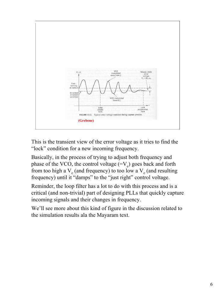
(Grebene)
This is the transient view of the error voltage as it tries to find the “lock” condition for a new incoming frequency.Basically, in the process of trying to adjust both frequency andphase of the VCO, the control voltage (=Ve) goes back and forth from too high a Ve (and frequency) to too low a Ve (and resulting frequency) until it “damps” to the “just right” control voltage.Reminder, the loop filter has a lot to do with this process and is a critical (and non-trivial) part of designing PLLs that quickly capture incoming signals and their changes in frequency.We’ll see more about this kind of figure in the discussion related to the simulation results ala the Mayaram text.
7
Block Diagram of PLL*
F(s) A
VCO
νp(s) νf(s) νo(s)Φi(s)
Φosc(s)
Φcomp(s)
*Notation--per K. Mayaram book (see slides at end of these notes AND second half of notes in “course reader”)
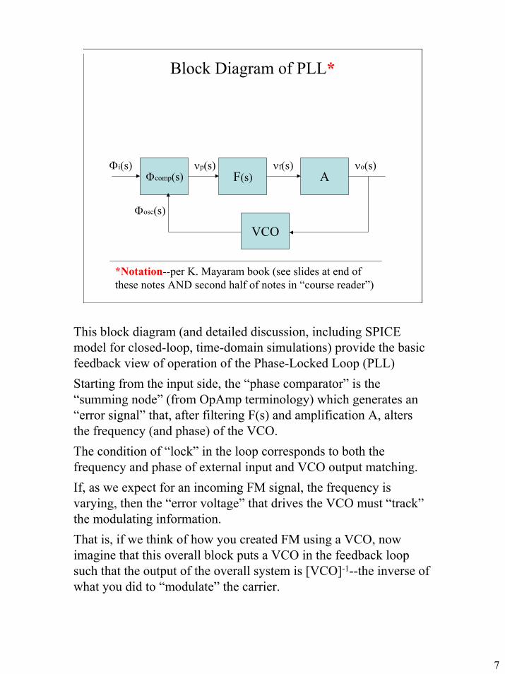
This block diagram (and detailed discussion, including SPICE model for closed-loop, time-domain simulations) provide the basic feedback view of operation of the Phase-Locked Loop (PLL)Starting from the input side, the “phase comparator” is the “summing node” (from OpAmp terminology) which generates an “error signal” that, after filtering F(s) and amplification A, alters the frequency (and phase) of the VCO.The condition of “lock” in the loop corresponds to both the frequency and phase of external input and VCO output matching.If, as we expect for an incoming FM signal, the frequency is varying, then the “error voltage” that drives the VCO must “track” the modulating information.That is, if we think of how you created FM using a VCO, now imagine that this overall block puts a VCO in the feedback loop such that the output of the overall system is [VCO]-1--the inverse of what you did to “modulate” the carrier.
8
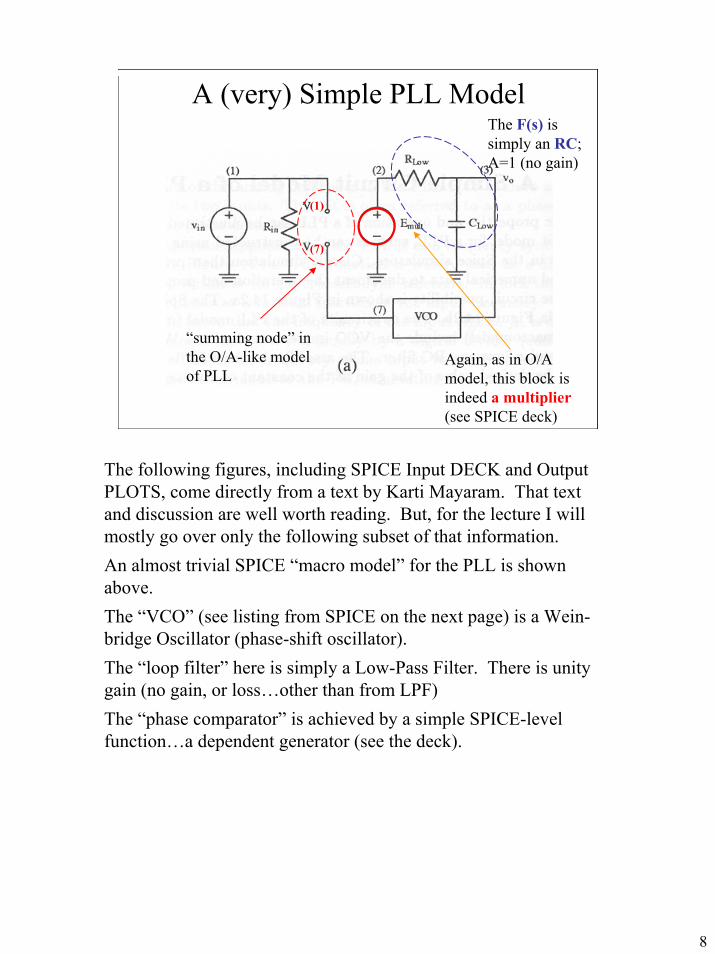
A (very) Simple PLL Model
“summing node” in the O/A-like model of PLL
Again, as in O/A model, this block is indeed a multiplier(see SPICE deck)
The F(s) is simply an RC; A=1 (no gain)
(1)
(7)
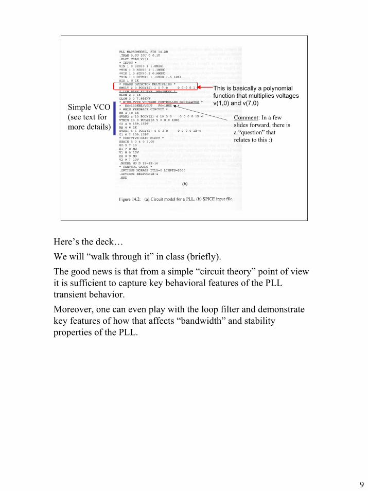
The following figures, including SPICE Input DECK and Output PLOTS, come directly from a text by Karti Mayaram. That text and discussion are well worth reading. But, for the lecture I will mostly go over only the following subset of that information.An almost trivial SPICE “macro model” for the PLL is shown above.The “VCO” (see listing from SPICE on the next page) is a Wein-bridge Oscillator (phase-shift oscillator).The “loop filter” here is simply a Low-Pass Filter. There is unity gain (no gain, or loss…other than from LPF)The “phase comparator” is achieved by a simple SPICE-level function…a dependent generator (see the deck).
9
This is basically a polynomial function that multiplies voltages v(1,0) and v(7,0)Simple VCO
(see text for more details)
Comment: In a few slides forward, there is a “question” that relates to this :)
Here’s the deck…We will “walk through it” in class (briefly).The good news is that from a simple “circuit theory” point of view it is sufficient to capture key behavioral features of the PLL transient behavior.Moreover, one can even play with the loop filter and demonstratekey features of how that affects “bandwidth” and stability properties of the PLL.
10
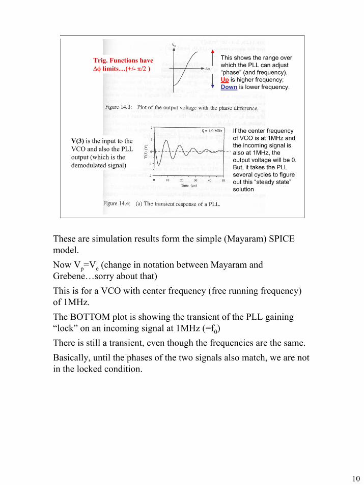
If the center frequency of VCO is at 1MHz and the incoming signal is also at 1MHz, the output voltage will be 0. But, it takes the PLL several cycles to figure out this “steady state” solution
This shows the range over which the PLL can adjust “phase” (and frequency). Up is higher frequency; Down is lower frequency.
V(3) is the input to the VCO and also the PLL output (which is the demodulated signal)
Trig. Functions have ∆φ limits…(+/- π/2 )
These are simulation results form the simple (Mayaram) SPICE model.Now Vp=Ve (change in notation between Mayaram and Grebene…sorry about that)This is for a VCO with center frequency (free running frequency)of 1MHz.The BOTTOM plot is showing the transient of the PLL gaining “lock” on an incoming signal at 1MHz (=f0)There is still a transient, even though the frequencies are the same.Basically, until the phases of the two signals also match, we are not in the locked condition.
11
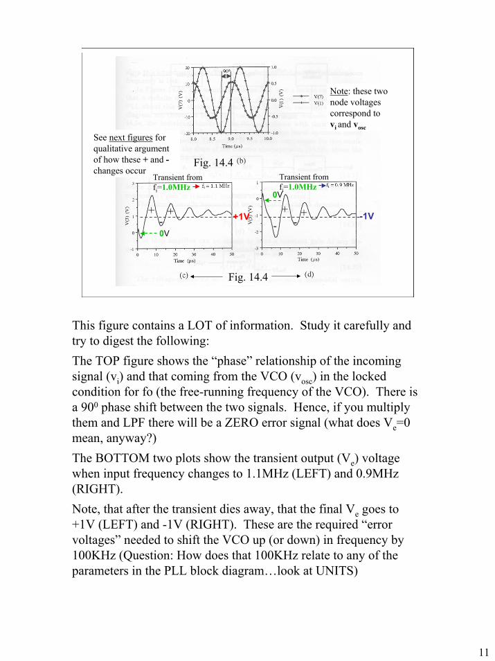
+1V -1V
0V
0V
Note: these two node voltages correspond to vi and vosc
+-
+
See next figures for qualitative argument of how these + and -changes occur
Fig. 14.4
Fig. 14.4
+-
+-
Transient from fi=1.0MHz
Transient from fi=1.0MHz
This figure contains a LOT of information. Study it carefully and try to digest the following:The TOP figure shows the “phase” relationship of the incoming signal (vi) and that coming from the VCO (vosc) in the locked condition for fo (the free-running frequency of the VCO). There is a 900 phase shift between the two signals. Hence, if you multiply them and LPF there will be a ZERO error signal (what does Ve=0 mean, anyway?)The BOTTOM two plots show the transient output (Ve) voltage when input frequency changes to 1.1MHz (LEFT) and 0.9MHz (RIGHT). Note, that after the transient dies away, that the final Ve goes to +1V (LEFT) and -1V (RIGHT). These are the required “error voltages” needed to shift the VCO up (or down) in frequency by 100KHz (Question: How does that 100KHz relate to any of the parameters in the PLL block diagram…look at UNITS)
12
The following set of slides try to explain, in the context of a multiplier acting as the “phase comparator,” how the input (vi(t)) and the oscillator (VCO output=vosc.(t)) combine to create the signal called out as X. Here are a few key points:
These waveforms get low-pass filtered; hence we are really looking at the averages--called out as “+” and “-”
These “+” and “-” changes in turn cause the VCO to move to higher and lower frequencies respectively (see for example Fig. 14.4)
Since these changes occur over a small number of cycles, they are far from the complete story, however they also help to illustrate issues concerning the “phase” part of the story…
Namely, when the lock condition is achieved there is a very specific phase relationship required (∆φ as indicated in Fig. 14.3)
The above discussion is a “warm up” for the following slides. Hence, there isn’t much to add here in the “notes” comments.
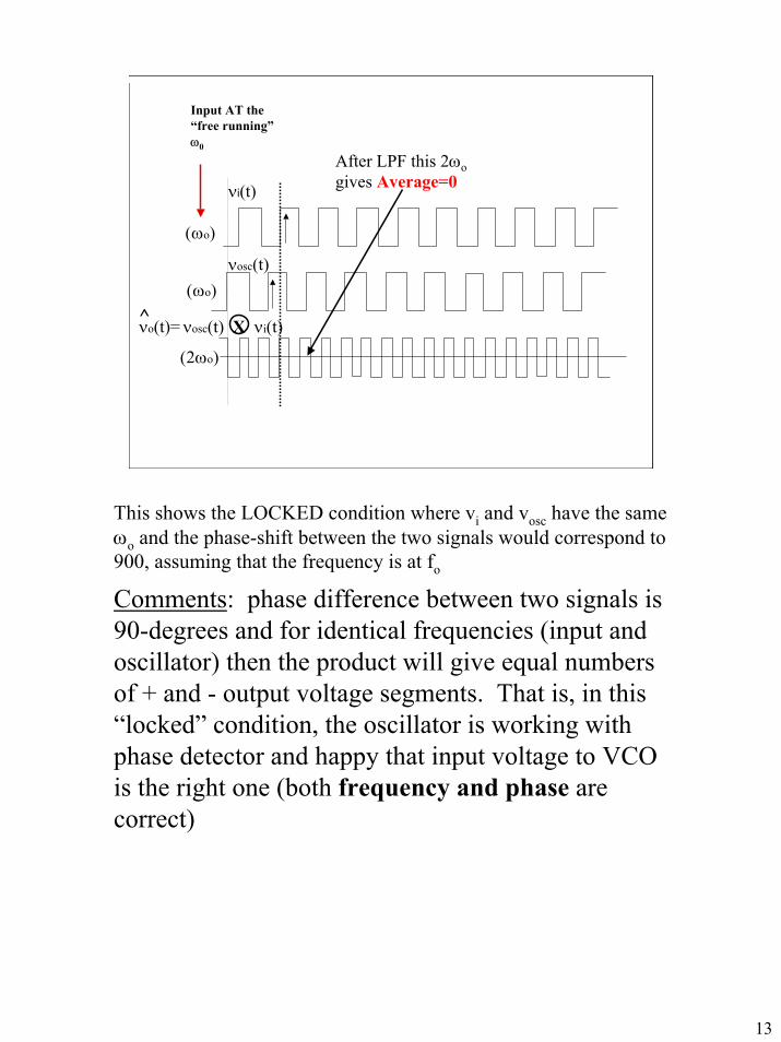
13
(ωo)
νi(t)
νosc(t)(ωo)
(2ωo)
νosc(t) X νi(t)νo(t)=^
After LPF this 2ωogives Average=0
Input AT the “free running” ω0
This shows the LOCKED condition where vi and vosc have the same ωo and the phase-shift between the two signals would correspond to 900, assuming that the frequency is at fo
Comments: phase difference between two signals is 90-degrees and for identical frequencies (input and oscillator) then the product will give equal numbers of + and - output voltage segments. That is, in this “locked” condition, the oscillator is working with phase detector and happy that input voltage to VCO is the right one (both frequency and phase are correct)
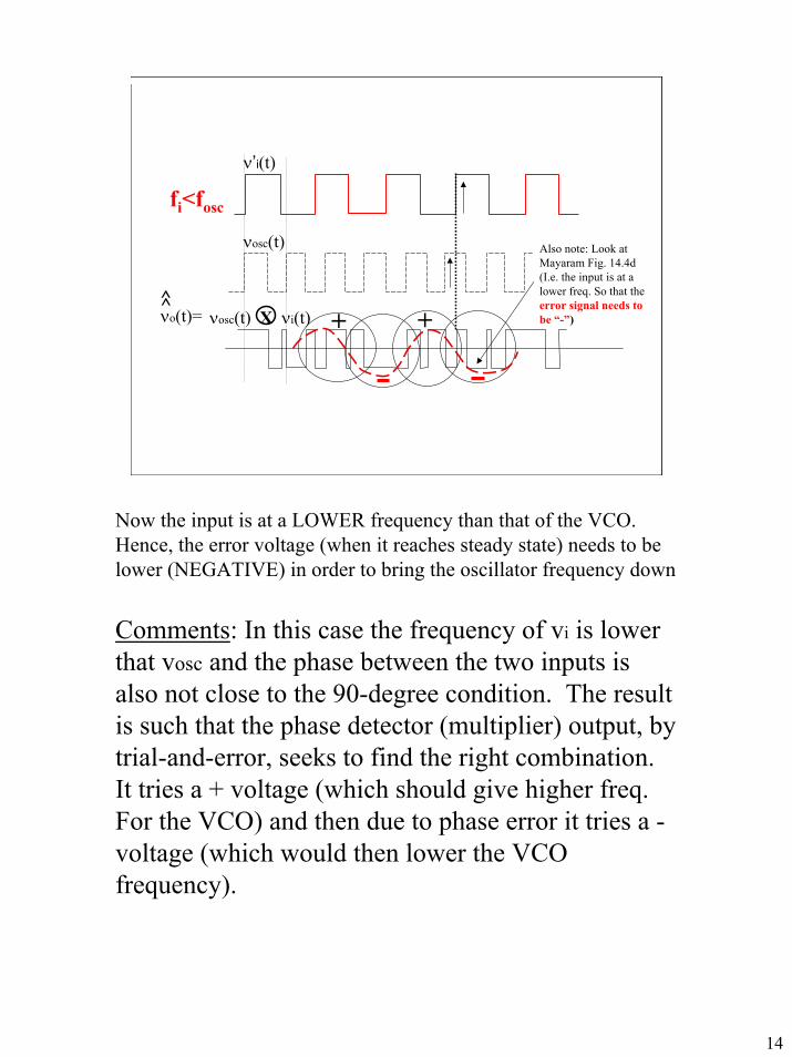
14
νosc(t)
νosc(t) X νi(t) + +
Also note: Look atMayaram Fig. 14.4d (I.e. the input is at a lower freq. So that the error signal needs to be “-”)
^νo(t)=^
ν’i(t)
fi<fosc
Now the input is at a LOWER frequency than that of the VCO. Hence, the error voltage (when it reaches steady state) needs to be lower (NEGATIVE) in order to bring the oscillator frequency down
Comments: In this case the frequency of vi is lower that vosc and the phase between the two inputs is also not close to the 90-degree condition. The result is such that the phase detector (multiplier) output, by trial-and-error, seeks to find the right combination. It tries a + voltage (which should give higher freq. For the VCO) and then due to phase error it tries a -voltage (which would then lower the VCO frequency).
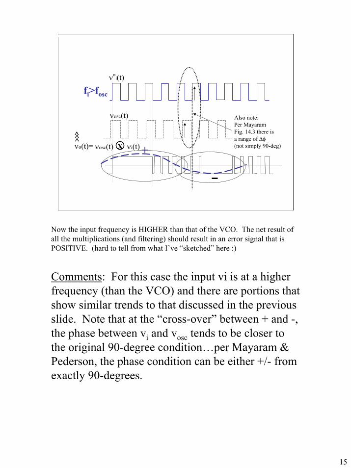
15
νosc(t)
νosc(t) X νi(t) +
Also note:Per MayaramFig. 14.3 there isa range of ∆φ(not simply 90-deg)
ν”i(t)
^νo(t)=^^
fi>fosc
Now the input frequency is HIGHER than that of the VCO. The net result of all the multiplications (and filtering) should result in an error signal that is POSITIVE. (hard to tell from what I’ve “sketched” here :)
Comments: For this case the input vi is at a higher frequency (than the VCO) and there are portions that show similar trends to that discussed in the previous slide. Note that at the “cross-over” between + and -, the phase between vi and vosc tends to be closer to the original 90-degree condition…per Mayaram & Pederson, the phase condition can be either +/- from exactly 90-degrees.
16
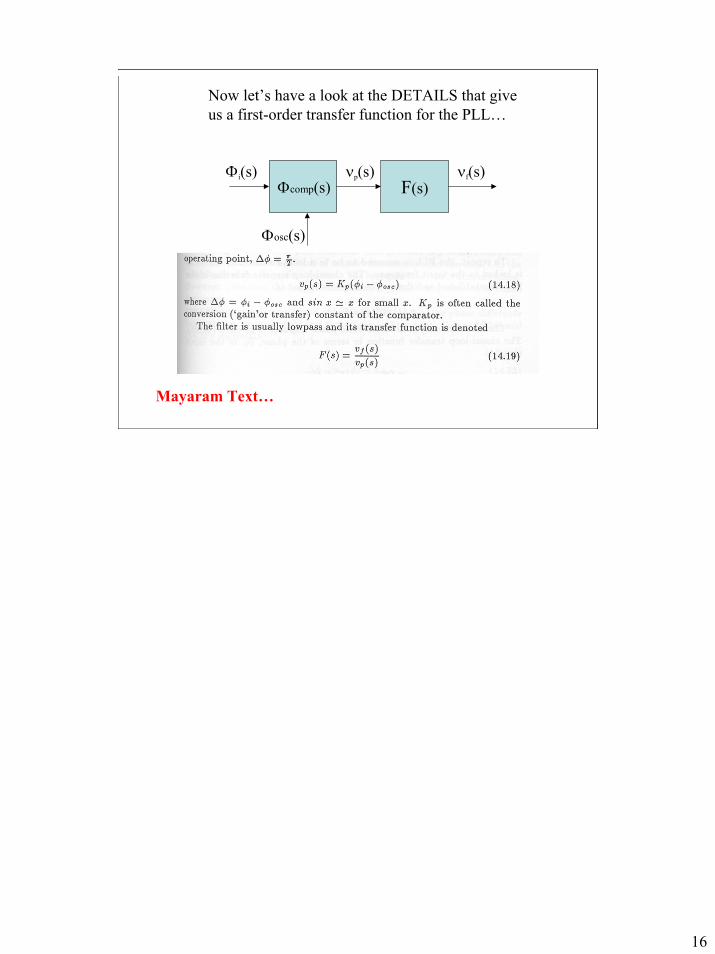
Now let’s have a look at the DETAILS that give us a first-order transfer function for the PLL…
F(s)νp(s) νf(s)Φi(s)
Φosc(s)
Φcomp(s)
Mayaram Text…
17
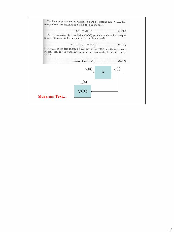
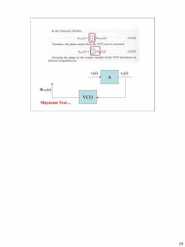
Aνf(s) νo(s)
VCO
ωosc(s)
Mayaram Text…
18
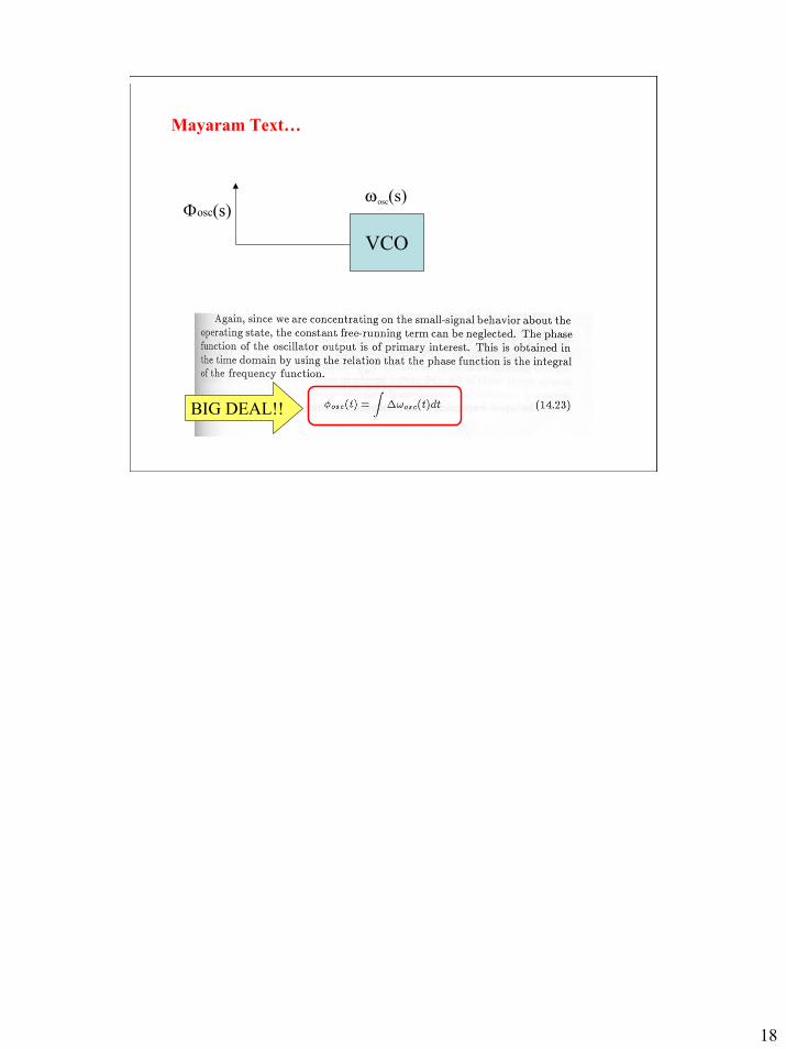
VCO
Φosc(s)
BIG DEAL!!
ωosc(s)
Mayaram Text…
19
Aνf(s) νo(s)
VCO
Φosc(s)
Mayaram Text…
20
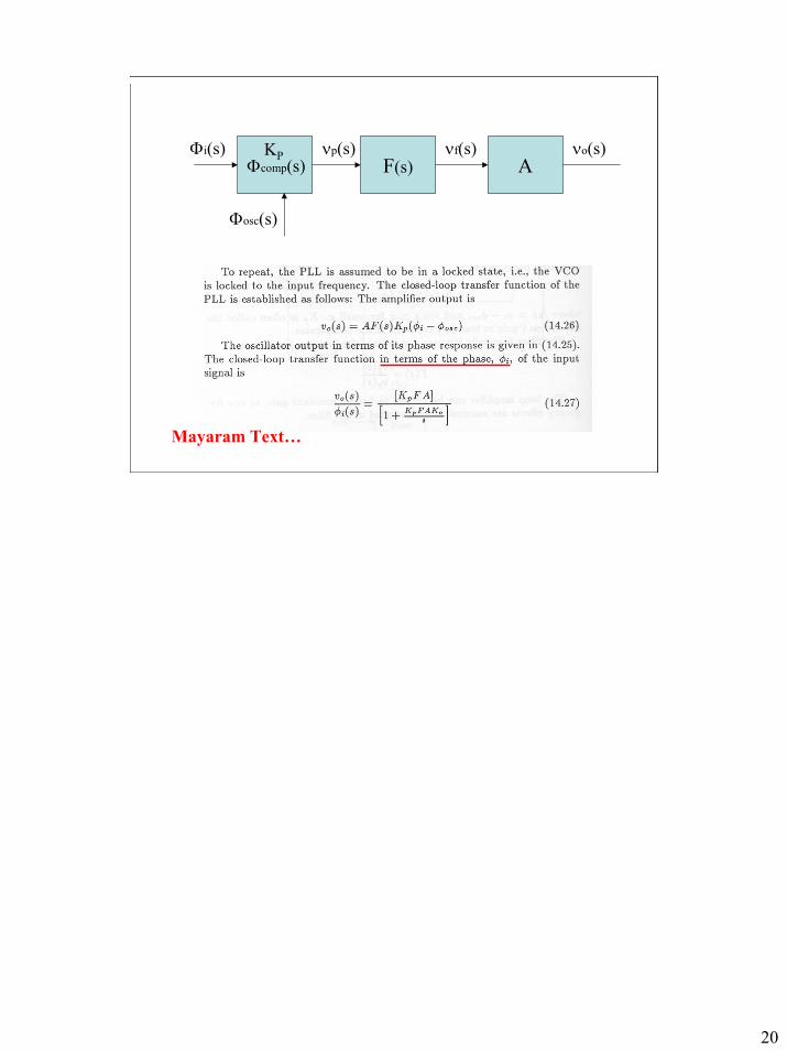
F(s) Aνp(s) νf(s) νo(s)Φi(s)
Φosc(s)
Φcomp(s)KP
Mayaram Text…
21
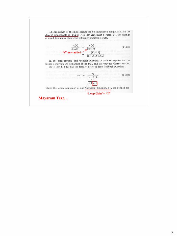
“s” now added
“Loop Gain”~ “T”
Mayaram Text…
22
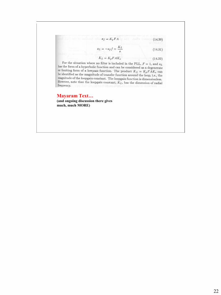
Mayaram Text…(and ongoing discussion there gives much, much MORE)


![EC0804-PLL [Modo de compatibilidad]€¦ · (PLL) 1 Capítulo 4 Lazos enganchados en fase. PLL Aplicaciones de los PLL Síntesis de frecuencia Partiendo de un oscilador patrón (f0),](https://img.pdfslide.tips/doc/110x75/5e8e438d8741af3761030a0b/ec0804-pll-modo-de-compatibilidad-pll-1-captulo-4-lazos-enganchados-en-fase.jpg)