Embed Size (px)
Citation preview
Thermopower and Conductance of Single
Thermopower and Conductance of Single
Molecule Junctions and Atomic Contacts
Thermopower and Conductance of Single
Molecule Junctions and Atomic Contacts
Universidad
Thermopower and Conductance of Single
Molecule Junctions and Atomic Contacts
Charalambos Evangeli
Universidad
Thermopower and Conductance of Single
Molecule Junctions and Atomic Contacts
Charalambos Evangeli
Madrid 2014
Universidad Autónoma
Thermopower and Conductance of Single
Molecule Junctions and Atomic Contacts
Charalambos Evangeli
Madrid 2014
Autónoma de Madrid
Thermopower and Conductance of Single
Molecule Junctions and Atomic Contacts
Charalambos Evangeli
Madrid 2014
de Madrid
Thermopower and Conductance of Single
Molecule Junctions and Atomic Contacts
de Madrid
Thermopower and Conductance of Single-
Molecule Junctions and Atomic Contacts -

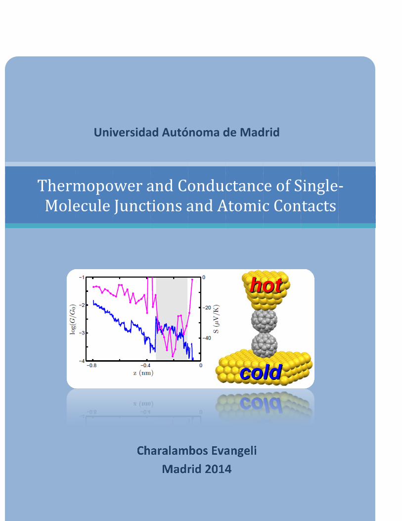
Cover: Conductance at 100 mV (blue) and thermopower (magenta), simultaneously
acquired, during the formation of the C60 dimer. In this measurement,the
temperature difference between the tip and the substrate was �� = 12K.

Thermopower and Conductance of Single-
Molecule Junctions and Atomic Contacts
Memoria presentada por
Charalambos Evangeli
para optar al grado de Doctor en Ciencias Físicas por la
Universidad Autónoma de Madrid
Dirigida por
Nicolás Agraït de la Puente
Departamento de Física de la Materia Condensada
Madrid, Noviembre 2014

Thermopower and Conductance of Single-
Molecule Junctions and Atomic Contacts
Thesis Presented by
Charalambos Evangeli
for the degree of Doctor in Physics by Universidad Autónoma de
Madrid
Thesis Supervisor
Nicolás Agraït de la Puente
Department of Condensed Matter Physics
Madrid, November 2014

Thesis committee:
Prof. Julio Gómez Herrero (Universidad Autónoma de Madrid) Prof. Jan M. van Ruitenbeek (Leiden University) Prof. Juan Carlos Cuevas Rodríguez (Universidad Autónoma de Madrid) Prof. Colin J. Lambert (University of Lancaster) Prof. José Ignacio Pascual Chico (CIC nanoGUNE)
This work has been supported by the European Union (FP7) through
programs ITN “FUNMOLS” Project Number 212942, ELFOS and by the
A.G. Leventis Foundation.

Acknowledgements
This work has been the result of the collaboration of many people throughout the
last 5 years. I would like to acknowledge everybody that helped, with the hope that
I will not forget anybody.
First, a heartfelt thanks to my supervisor Nicolás Agraït, who trusted me and gave
me the opportunity to work on this project. His daily guidance and support in the
lab was indispensable. He was always available and patient with me, spending time
discussing the problems which arose during the realization of this work. I learned a
lot from him about experiments, and Physics in general.
Teresa González and Edmund Leary, who taught me and guided me in the
laboratory. They were there, ready to help with every problem. We spent many
long hours discussing a multitude of issues, and without their invaluable input this
project would never have come to fruition.
Thanks to José Gabriel Rodrigo, for helping with issues surrounding the
experimental setup. Andrés Buendía and Rosa Díez, Santiago Marquez and Juan
Benayas our technicians, for all their help in designing and constructing the
experimental setups.
Professor Colin Lambert, for the four months I spent with his group and all the
collaboration we had during all these years, and also for the many nights of “Golden
Lion” entertainment. Thanks to all his group in Lancaster University; David, David
(with the long hair), Rachel, Iain, Ali, Steven and Csaba for the patience they had to
teach and collaborate with an experimentalist! In particular, Kataline, for teaching
me about theoretical calculations, helping me with settling, and all the collaboration
we had. Vasilis, Thanos, Christos for making more pleasant my stay in Lanchaster.
Professor Michele Calame, for the short stay at his group in the University of Basel,
all the people of his group and especially Cornelia, Jan and Toni.
Thanks to all the people in our group: Aday, Jorge, Laura, Siya, Guille, for tolerating
my swearing in Greek, particularly during the last few months. Siya, for being a
great partner in the lab, working together, even on the overnight experiments, and
being a gracious tour guide in India. Laurita, the only optimistic person in the lab,
for helping me with translations; Aday, for the many hours of group therapy, with
and without alcohol, for our lab-complaints; Guille, for elevating the atmosphere of
the lab with early morning calls for las camisetas amarillas and Jorge (Giorgos), for
always being “focusado”.
Thanks to the people from the Low Temperatures Lab. Mersak, the big brother, for
his help and support from the first day I entered the lab. Your talent for
communicating through “Franglishñolbic” was very much appreciated. Tomás, for
his noisy pump (as he was saying: All your results are thanks to my pump). Bisher,
for his help with communication issues in Spanish, especially the first few months in
the lab. Augusto, Ana, Andrés, Roberto, Edwin, Antón, Isa and Pepe for making daily
life in the lab better with their humour and energy. The two senior PhD students of
my group, Carlos and Andrés, for teaching me about experimental techniques.
Manuel and Jan, for the Fontana Friday nights. Jan, thanks for insisting on
disconnecting from the stress of the week. Thanks also to the people on the other
floors - Ahmad, Michelle, Curro, Antonio, Michelle, Mohamed, Amjad, Guillermo,
David, Juanpe …apologies to anyone I have omitted!
The people of the FUNMOLS network, for the nice moments of Net-working and
Not-working during the meetings. Andrea, for his “sexy” molecules, all the parties in
Madrid and trips; Toni, the relaxed guy; Pavel, for all the discussions with a guy who
knows about the real difficulties of life; Murat, my Turkish friend who showed me
that friendships between people go beyond national issues; lastminuteAndres.es;
Marta, for our discussions about life; Hui, the optimistic girl of the network and
Giorgio, the serious one, and Mateus, my Polish twin. Also, all the professors of the
Network for the discussions, scientific collaboration and various contributions to
our progress; Nazario Martín, for providing us with molecules; Martin Bryce, Heike
Riel, Dirk Guldi, Thomas Wandlowski and Jan Jeppesen.
During this thesis I had the opportunity to collaborate with people from other
groups and Universities in order to complete this work. Juan Carlos Cuevas and his
group for the theoretical calculations, and for shattering the stereotypes regarding
theoretical physicists (i.e. thanks for explaining things to me in a clear and simple
manner). Prof. M. Nielsen, for synthesizing the molecules and Prof. G. Solomon, for
the theoretical calculations.
Thanks to the professors of the laboratory; Miguel Ángel Ramos, Hermann
Suderow, Sebastián Vieira and Gabino Rubio-Bollinger. Also to the secretaries of the
Department Elsa Sánchez and Luisa Carpallo.
It would not be possible not to mention my friends outside the laboratory for their
support, especially in the last difficult year; The QC group - Mic, Nicole, Neil,
Patricia, Silvia, Marilena and Andrea for the BBQ therapy; and also Marco, Vanessa,
Nuria and Pablo for all help and the nice moments. Neil – thank you - for your
patience reading and understanding everything about “the expansion of the tip
when it is heated, and its subsequent approach towards the sample”, in order to
correct the English of this thesis.
All my friends in Cyprus and Greece and my cousins for the nice holidays we had
together during all these years, giving me the energy to continue. Kyras, Mouskos,
Pomos, Giorkos, Andreas, Petros, Tomis, Mpampis, Michalis, Natasa, Christoforos,
Christos, Vasilis, Mikela, Louda, Achileas and Christodoulos.
I would like also to thank my football team APOEL for all the great moments in the
Champions League in Porto, Lyon, Madrid, London, Barcelona and Paris. Short one-
day breaks from the daily routine with amazing memories.
Thanks to everybody that I forgot to mention!
Finally, and most importantly, my parents Andreas and Paraskevi. They supported
me in everything during these years. I owe everything to them. The last wish of my
father was to be here with me for this important moment of my life but
unfortunately he couldn’t make it.


Figures and Tabl
Abstract
Resumen
Part I: Background
1.1
1.2
1.3
1.4
References
2.1
2.2
2.3
2.4
2.5
References
3.1
3.2
Figures and Tabl
Abstract ................................
Resumen ................................
Part I: Background
Quantum Electron Transport
1.1 Introduction
1.2 The Landauer formula
1.3 Quantum tunneling
1.4 Quantum transport through molecular junctions
References ................................
Thermoelectric Effects
2.1 Thermoelectric effect
2.2 The Seebeck effect
2.3 Thermocouple
2.4 Thermoelectric power generation and figure of merit
2.5 Thermopower at the nanoscale
2.5.1 Thermopower of a nanojunction
2.5.2 Energy levels of the Junction vs Thermopower
2.5.3 Quantum interference and thermopower
References ................................
Experimental Tools
3.1 Functioning of the Scanning Tunneling Microscope
3.2 Room temperature STM
Figures and Table Index ................................
................................
................................
Part I: Background ................................
Quantum Electron Transport
Introduction ................................
The Landauer formula
Quantum tunneling
Quantum transport through molecular junctions
................................
Thermoelectric Effects ................................
Thermoelectric effect
The Seebeck effect
Thermocouple ................................
Thermoelectric power generation and figure of merit
Thermopower at the nanoscale
Thermopower of a nanojunction
Energy levels of the Junction vs Thermopower
Quantum interference and thermopower
................................
Experimental Tools ................................
Functioning of the Scanning Tunneling Microscope
Room temperature STM
................................
................................................................
................................................................
................................................................
Quantum Electron Transport ................................
................................
The Landauer formula ................................
Quantum tunneling ................................
Quantum transport through molecular junctions
................................................................
................................
Thermoelectric effect ................................
The Seebeck effect ................................
................................
Thermoelectric power generation and figure of merit
Thermopower at the nanoscale
Thermopower of a nanojunction
Energy levels of the Junction vs Thermopower
Quantum interference and thermopower
................................................................
................................
Functioning of the Scanning Tunneling Microscope
Room temperature STM ................................
................................................................
................................................................
................................................................
................................
................................
................................................................
................................................................
................................................................
Quantum transport through molecular junctions
................................................................
................................................................
................................................................
................................................................
................................................................
Thermoelectric power generation and figure of merit
................................
Thermopower of a nanojunction ................................
Energy levels of the Junction vs Thermopower
Quantum interference and thermopower
................................................................
................................................................
Functioning of the Scanning Tunneling Microscope
................................................................
.........................................................
................................
................................
..............................................................
................................................................
...............................................................
................................
................................
Quantum transport through molecular junctions ................................
................................
................................
................................
................................
...........................................................
Thermoelectric power generation and figure of merit .............................
................................................................
................................
Energy levels of the Junction vs Thermopower ................................
Quantum interference and thermopower ................................
................................
......................................................
Functioning of the Scanning Tunneling Microscope ................................
................................
Table of Contents
.........................
................................................
...............................................
..............................
.......................................
...............................
...............................................
...................................................
.....................................
.............................................
.................................................
................................................
....................................................
...........................
.............................
................................
.......................................................
................................
........................................
.............................................
......................
................................
............................................
Table of Contents
......................... 1
................ 5
............... 9
.............................. 13
....... 15
............................... 15
............... 16
................... 19
..... 21
............. 23
................. 25
................ 25
.................... 27
........................... 32
............................. 33
................................ 36
....................... 36
................................. 40
........ 42
............. 44
...................... 47
................................. 47
............ 49
Table of Contents
3.2.1
3.2.2
3.2.3
3.2.4
3.3
References
Simultaneous Thermopower and Conductance Measurement Technique
4.1
4.2
4.3
References
Part II: Experimental Results
Engineering the Thermopower of Fullerene Molecular Junctions
5.1
5.1.1
5.1.2
5.2
5.3
5.4
References
Quantum Thermopower of Metallic Nanocontacts
6.1
6.2
contacts
Table of Contents
3.2.1 The piezotube
3.2.2 Tip holder and the heater
3.2.3 STM electronics
3.2.4 Current to voltage amplifier
Low temperature STM
References ................................
Simultaneous Thermopower and Conductance Measurement Technique
Introduction
The technique
Thermopower circuit
References ................................
Part II: Experimental Results
Engineering the Thermopower of Fullerene Molecular Junctions
Conductance characterization of single
5.1.1 Single-
5.1.2 Double
Conductance of double
Simultaneous
92
Conclusions
References ................................
Quantum Thermopower of Metallic Nanocontacts
Introduction
Simultaneous thermopower and conductance measurements of Au and Pt
contacts ................................
The piezotube ................................
Tip holder and the heater
STM electronics ................................
Current to voltage amplifier
Low temperature STM ................................
................................................................
Simultaneous Thermopower and Conductance Measurement Technique
uction ................................
The technique ................................
Thermopower circuit -voltage offsets
................................................................
Part II: Experimental Results ................................
Engineering the Thermopower of Fullerene Molecular Junctions
Conductance characterization of single
-C60 molecular junctions
Double-C60 molecular Junctions
Conductance of double-C
Simultaneous S and G measurements of single
Conclusions ................................
................................................................
Quantum Thermopower of Metallic Nanocontacts
Introduction ................................
multaneous thermopower and conductance measurements of Au and Pt
................................................................
................................
Tip holder and the heater ................................
................................
Current to voltage amplifier ................................
................................
................................
Simultaneous Thermopower and Conductance Measurement Technique
................................................................
................................................................
voltage offsets
................................
................................
Engineering the Thermopower of Fullerene Molecular Junctions
Conductance characterization of single
molecular junctions ................................
molecular Junctions ................................
C60 junctions using DFT theory
measurements of single
................................................................
................................
Quantum Thermopower of Metallic Nanocontacts
................................................................
multaneous thermopower and conductance measurements of Au and Pt
................................
................................................................
................................
................................................................
................................
................................................................
................................................................
Simultaneous Thermopower and Conductance Measurement Technique
................................
................................
voltage offsets ................................
................................................................
................................................................
Engineering the Thermopower of Fullerene Molecular Junctions
Conductance characterization of single- and double
................................
................................
junctions using DFT theory
measurements of single- and double
................................
................................................................
Quantum Thermopower of Metallic Nanocontacts ................................
................................
multaneous thermopower and conductance measurements of Au and Pt
................................................................
.....................................................
................................................................
..................................................
...............................................................
................................
................................
Simultaneous Thermopower and Conductance Measurement Technique
................................................................
.............................................................
........................................................
................................
...............................................
Engineering the Thermopower of Fullerene Molecular Junctions ................
and double-C60 junctions
...........................................................
.........................................................
junctions using DFT theory ............................
and double-C60
..............................................................
................................
................................
.............................................................
multaneous thermopower and conductance measurements of Au and Pt
...............................................
.....................51
..................................52
..................53
...............................54
...............................................55
..............................................57
Simultaneous Thermopower and Conductance Measurement Technique.... 59
................................59
.............................63
........................65
..............................................69
............... 71
................ 73
junctions ...........73
...........................74
.........................79
............................87
60 junctions
.............................. 102
........................................... 103
..................................... 107
............................. 107
multaneous thermopower and conductance measurements of Au and Pt
............... 108

6.3
6.4
References
7.1
7.2
7.3
derivatives
7.4
References
8.1
8.2
8.3
8.4
References
General Conclusions
Conclusiones Generales
Appendices
Appendix A
Appendix B
Appendix C
Appendix D
Appendix E
Appendix F
Appendix G
6.3 Theoretical calculations on the
6.4 Conclusions
References ................................
Enhancing the Thermopower of OPE Molecular Junctions
7.1 Introduction
7.2 Conductance characterization of the OPE derivatives
7.3 Simultaneous thermopower and conductance measurements of the OPE
derivatives ................................
7.4 Conclusions
References ................................
Exploring Fullerenes as Linkers
8.1 Introduction
8.2 Formation o
8.3 DFT calculations on the single
8.4 Conclusions
References ................................
General Conclusions
Conclusiones Generales
Appendices ................................
Appendix A
Appendix B
Appendix C
Appendix D
Appendix E
Appendix F
Appendix G
Theoretical calculations on the
Conclusions ................................
................................
Enhancing the Thermopower of OPE Molecular Junctions
Introduction ................................
Conductance characterization of the OPE derivatives
Simultaneous thermopower and conductance measurements of the OPE
................................
Conclusions ................................
................................
Exploring Fullerenes as Linkers
Introduction ................................
Formation of single
DFT calculations on the single
Conclusions ................................
................................
General Conclusions ................................
Conclusiones Generales ................................
................................
Piezotube calibration
Drift estimation
Tip temperature calibration
Thermopower offset due to the tip
Ideal-Non ideal Op
C60 deposition
Dumbbell molecular wires deposition
Theoretical calculations on the S
................................
................................................................
Enhancing the Thermopower of OPE Molecular Junctions
................................
Conductance characterization of the OPE derivatives
Simultaneous thermopower and conductance measurements of the OPE
................................................................
................................
................................................................
Exploring Fullerenes as Linkers ................................
................................
f single-C60 dumbbell junctions
DFT calculations on the single-C
................................
................................................................
................................
................................
................................................................
Piezotube calibration ................................
Drift estimation ................................
Tip temperature calibration
Thermopower offset due to the tip
Non ideal Op-Amp
deposition ................................
l molecular wires deposition
S and G of Au and Pt atomic contacts
................................................................
................................................................
Enhancing the Thermopower of OPE Molecular Junctions
................................................................
Conductance characterization of the OPE derivatives
Simultaneous thermopower and conductance measurements of the OPE
................................................................
................................................................
................................................................
................................
................................................................
dumbbell junctions ................................
60 dumbbell junction
................................................................
................................................................
................................................................
................................................................
................................
................................
................................................................
Tip temperature calibration ................................
Thermopower offset due to the tip-connecting lead
................................
................................................................
l molecular wires deposition
of Au and Pt atomic contacts
..............................................................
................................
Enhancing the Thermopower of OPE Molecular Junctions ..........................
.............................................................
Conductance characterization of the OPE derivatives ............................
Simultaneous thermopower and conductance measurements of the OPE
................................
..............................................................
................................
................................................................
.............................................................
................................
dumbbell junction .............................
..............................................................
................................
..........................................................
....................................................
................................................................
................................................................
................................
........................................................
connecting lead
..............................................................
................................
l molecular wires deposition ................................
Table of Contents
of Au and Pt atomic contacts ...
..............................
...........................................
..........................
.............................
............................
Simultaneous thermopower and conductance measurements of the OPE
...........................................
..............................
...........................................
..................................
.............................
............................................
.............................
..............................
...........................................
..........................
....................
.......................................
...................................
............................................
........................
connecting lead ..................
..............................
..............................................
.........................................
Table of Contents
... 114
.............................. 118
........... 119
.......................... 121
............................. 121
............................ 123
Simultaneous thermopower and conductance measurements of the OPE
........... 125
.............................. 131
........... 132
.. 133
............................. 133
............ 134
............................. 143
.............................. 147
........... 148
.......................... 151
.................... 153
....... 157
... 159
............ 164
........................ 168
.................. 173
.............................. 177
.............. 179
......... 182
Table of Contents
Appendix H
Appendix I
Appendix J
Appendix K
Publication List
Table of Contents
SampleAppendix H
Conductance of Au atomic contacAppendix I
Green’s FunctionsAppendix J
Quantum transport CalculationsAppendix K
Publication List ................................
Sample-tip cleanliness characterization
Conductance of Au atomic contac
Green’s Functions
Quantum transport Calculations
................................
tip cleanliness characterization
Conductance of Au atomic contac
Green’s Functions ................................
Quantum transport Calculations
................................................................
tip cleanliness characterization ................................
Conductance of Au atomic contacts ................................
................................................................
Quantum transport Calculations ................................
................................................................
................................
................................
................................
.................................................
................................
...................................... 184
........................................... 186
........................................ 190
................. 194
.................................. 199

Figure 1
Figure 1
Figure 1
Figure 2
Figure 2
Figure 2
Figure 2
Figure 2
Figure 2
Figure 2
Figure 2
Figure 3
Figure 3
Figure 3
Figure 3
Figure 3
Figure 3
Figure 3
Figure 3
Figure 4
Figure 4
junctions.
Figure 4
................................
Figure 4
Figure 4
Figure 5
Figure 5
Figure 5
Figure 5
Figure 5
Figure 1-1: Transport through a nanojunction.
Figure 1-2: Quantum electron tunneling.
Figure 1-3: Level schemes for molecular junction.
Figure 2-1: The Seeb
Figure 2-2: Seebeck coefficients for different metals for different temperatures.
Figure 2-3: Schematic of a the
Figure 2-4: Thermoelectric Generator.
Figure 2-5: Thermopower at the macro
Figure 2-6: Energy level diagram of the thermopower in a molecular junction.
Figure 2-7: Relation of transmission function and thermopower.
Figure 2-8: Quantum interference in molecular junctions.
Figure 3-1: The basic principle of STM function.
Figure 3-2: The two scanning modes of a STM.
Figure 3-3: The Room temperature STM used for the experiments.
Figure 3-4: Schematics of the piezotube.
Figure 3-5: Tip holders of the STM.
Figure 3-6: Schematic
Figure 3-7: Circuits of the current amplifiers used in the experiments.
Figure 3-8: The Low Temp
Figure 4-1: STM Break Junction technique as presented by Tao.
Figure 4-2: Techniques r
junctions. ................................
Figure 4-3: Simultaneous thermopower and conductance measurements technique.
................................
Figure 4-4: Effective circuit of the STM.
Figure 4-5: Configuration for measuring the offset
Figure 5-1: Tip positioning on C
Figure 5-2: Approach
Figure 5-3: Conductance histograms of Au
Figure 5-4: Transferring a C
Figure 5-5: Imaging with a C
1: Transport through a nanojunction.
2: Quantum electron tunneling.
3: Level schemes for molecular junction.
1: The Seebeck Effect.
2: Seebeck coefficients for different metals for different temperatures.
3: Schematic of a the
4: Thermoelectric Generator.
5: Thermopower at the macro
6: Energy level diagram of the thermopower in a molecular junction.
7: Relation of transmission function and thermopower.
8: Quantum interference in molecular junctions.
1: The basic principle of STM function.
2: The two scanning modes of a STM.
3: The Room temperature STM used for the experiments.
4: Schematics of the piezotube.
5: Tip holders of the STM.
6: Schematics of the function of a STM.
7: Circuits of the current amplifiers used in the experiments.
8: The Low Temperature STM used for the experiments.
1: STM Break Junction technique as presented by Tao.
2: Techniques reported for measuring the thermopower of molecular
................................
3: Simultaneous thermopower and conductance measurements technique.
................................................................
4: Effective circuit of the STM.
5: Configuration for measuring the offset
1: Tip positioning on C
2: Approach-retraction conductance traces of single
3: Conductance histograms of Au
4: Transferring a C60
5: Imaging with a C60
1: Transport through a nanojunction.
2: Quantum electron tunneling. ................................
3: Level schemes for molecular junction.
eck Effect. ................................
2: Seebeck coefficients for different metals for different temperatures.
3: Schematic of a thermocouple. ................................
4: Thermoelectric Generator. ................................
5: Thermopower at the macro- and nanoscale.
6: Energy level diagram of the thermopower in a molecular junction.
7: Relation of transmission function and thermopower.
8: Quantum interference in molecular junctions.
1: The basic principle of STM function.
2: The two scanning modes of a STM.
3: The Room temperature STM used for the experiments.
4: Schematics of the piezotube. ................................
5: Tip holders of the STM. ................................
s of the function of a STM.
7: Circuits of the current amplifiers used in the experiments.
erature STM used for the experiments.
1: STM Break Junction technique as presented by Tao.
eported for measuring the thermopower of molecular
................................................................
3: Simultaneous thermopower and conductance measurements technique.
................................................................
4: Effective circuit of the STM. ................................
5: Configuration for measuring the offset
1: Tip positioning on C60 molecule.
retraction conductance traces of single
3: Conductance histograms of Au
60 molecule on the tip.
60 and a bare Au tip.
1: Transport through a nanojunction. ................................
................................
3: Level schemes for molecular junction. ................................
................................................................
2: Seebeck coefficients for different metals for different temperatures.
................................
................................
and nanoscale.
6: Energy level diagram of the thermopower in a molecular junction.
7: Relation of transmission function and thermopower.
8: Quantum interference in molecular junctions.
1: The basic principle of STM function. ................................
2: The two scanning modes of a STM. ................................
3: The Room temperature STM used for the experiments.
................................
................................................................
s of the function of a STM. ................................
7: Circuits of the current amplifiers used in the experiments.
erature STM used for the experiments.
1: STM Break Junction technique as presented by Tao.
eported for measuring the thermopower of molecular
................................................................
3: Simultaneous thermopower and conductance measurements technique.
................................
................................
5: Configuration for measuring the offset �. ................................
molecule. ................................
retraction conductance traces of single
3: Conductance histograms of Au-C60-Au junctions.
molecule on the tip. ................................
and a bare Au tip. ................................
Figures and Tables Index
.........................................................
................................................................
................................
................................
2: Seebeck coefficients for different metals for different temperatures.
................................................................
................................................................
and nanoscale. ................................
6: Energy level diagram of the thermopower in a molecular junction.
7: Relation of transmission function and thermopower. .............................
8: Quantum interference in molecular junctions. ................................
........................................................
.........................................................
3: The Room temperature STM used for the experiments. .........................
................................................................
................................
................................
7: Circuits of the current amplifiers used in the experiments.
erature STM used for the experiments. ...........................
1: STM Break Junction technique as presented by Tao. ..............................
eported for measuring the thermopower of molecular
................................
3: Simultaneous thermopower and conductance measurements technique.
................................................................
................................................................
................................
..............................................................
retraction conductance traces of single-C60 junction
Au junctions. ................................
................................
................................
Figures and Tables Index
.........................
................................
....................................................
..................................................
2: Seebeck coefficients for different metals for different temperatures. ....
................................
......................................
..........................................
6: Energy level diagram of the thermopower in a molecular junction. .......
.............................
........................................
........................
.........................
.........................
...................................
............................................
......................................................
7: Circuits of the current amplifiers used in the experiments. .....................
...........................
..............................
eported for measuring the thermopower of molecular
...................................................
3: Simultaneous thermopower and conductance measurements technique.
...................................
....................................
............................................
..............................
junction. ............
...................................
....................................................
.....................................................
Figures and Tables Index
1
......................... 16
.................................. 20
.................... 22
.................. 28
.... 31
................................. 32
...... 34
.......... 37
....... 40
............................. 42
........ 43
........................ 48
......................... 49
......................... 50
... 51
............ 52
...................... 53
..................... 54
........................... 55
.............................. 60
................... 62
3: Simultaneous thermopower and conductance measurements technique.
... 64
.... 66
............ 67
.............................. 75
............ 76
... 78
.................... 80
..................... 81

Figures and Tables Index
2
Figure 5-6: − � curves on top of a C60 molecule with Au tip and on top of Au with a
C60 tip. .........................................................................................................................82
Figure 5-7: Formation of Au-C60-C60-Au junction. .......................................................84
Figure 5-8: Approach-retraction conductance curves and conductance histograms of
Au-C60-C60-Au Junction. ...............................................................................................85
Figure 5-9: Double C60 junctions of isolated C60 and C60s in clusters. .........................87
Figure 5-10: Quantum transport calculations for Au-C60-C60-Au junction. .................88
Figure 5-11: Quantum transport calculations for Au-C60-C60-Au junction while C60
sliding with respect to each other. .............................................................................90
Figure 5-12: Quantum transport calculations for Au-C60-C60-Au junction for different
orientations of the C60s. ..............................................................................................91
Figure 5-13: Approach and retraction traces of simultaneous conductance
thermopower measurements of Au-C60-Au junctions. ...............................................94
Figure 5-14: Approach and retraction traces of simultaneous conductance
thermopower measurements of Au- C60-C60-Au junctions. .........................................96
Figure 5-15: 2D-histograms of conductance with thermopower. ..............................97
Figure 5-16: DFT calculated results of thermopower and figure of merit for single-
and double-C60 junctions. ...........................................................................................99
Figure 5-17: Histograms of thermopower obtained experimentally and with DFT
calculations. ............................................................................................................. 101
Figure 6-1: Previous measurements on conductance and thermopower of Au atomic
contacts. .................................................................................................................. 109
Figure 6-2: Simultaneous measurement of the conductance and thermopower of
metallic atomic-size contacts. ................................................................................. 110
Figure 6-3: Simultaneous measurement of conductance and thermopower of Pt
atomic-size contacts. ............................................................................................... 111
Figure 6-4: Thermopower of Au and Pt atomic-size contacts. ................................ 112
Figure 6-5: Transition of the thermopower from atomic to large Au and Pt contacts.
................................................................................................................................. 113
Figure 6-6: Computed thermopower and conductance of Au and Pt atomic contacts.
................................................................................................................................. 115
Figure 6-7: Origin of the sign of the thermopower. ................................................ 117
Figure 7-1: Chemical structures of the three OPE compounds. ............................... 122
Figure 7-2: Conductance measurements on the OPEs derivatives. ......................... 124

Figures and Tables Index
3
Figure 7-3: Conductance and thermopower simultaneous measurement of molecular
junctions. ................................................................................................................. 126
Figure 7-4: Density plots of conductance and thermopower for the OPEs derivatives.
................................................................................................................................. 128
Figure 7-5: Average thermopower of the OPEs derivatives. .................................... 129
Figure 7-6: The logarithm of the transmission plotted against energy for OPE3,
OPE3-DTF, and OPE3-TTF. ....................................................................................... 130
Figure 8-1: Tip positioning on an individual dumbbell molecule. ............................ 135
Figure 8-2 Approach-retraction conductance curves and 2D-histograms showing the
tip contact to one C60 group. ................................................................................... 136
Figure 8-3: Au-dumbbell – dumbbell - Au junction. ................................................. 138
Figure 8-4: Images taken before and after the molecule transferred to the tip. .... 139
Figure 8-5 : Data showing the dumbbell, suspended from the tip, approaching and
retracting from the surface. .................................................................................... 140
Figure 8-6: Density Functional Theory calculations. ................................................ 144
Figure 8-7: A simplified model of the molecule-electrode system in our experiment.
................................................................................................................................. 146
Figure A-1: z calibration of the piezotube. ............................................................... 159
Figure A-2: x,y calibration of the piezotube without heater. ................................... 160
Figure A-3: Drift estimation from an atomic resolution image of graphene. .......... 165
Figure A-4: Measuring the drift by consecutive images. ......................................... 166
Figure A-5: Photo of the box where STM is placed. ................................................. 166
Figure A-6: Schematic of the tip holder with incorporated heater. ......................... 168
Figure A-7: Tip temperature estimation. ................................................................. 171
Figure A-8: Equivalent thermal circuit of the setup for the calculation of the
thermopower. .......................................................................................................... 173
Figure A-9: Absolute thermopower of bulk Au and Pt. ............................................ 175
Figure A-10: Equivalent circuit of an Ideal (left) and non-Ideal (right) Op-Amp. .... 177
Figure A-11: STM topographic images for different deposition procedures of C60. . 180
Figure A-12: STM topographic images for dumbbell molecular wires deposited with
drop casting. ............................................................................................................ 183
Figure A-13: Checking the cleanliness of a sample. ................................................. 184
Figure A-14: Conductance curves of Au atomic contacts. ....................................... 187

Figures and Tables Index
4
Figure A-15: Conductance of atomic contacts of gold as a result of small and large
indentation of the substrate. ................................................................................... 188
Figure A-16: Conductor with transmission probability � connected to two large
contacts through two leads. .................................................................................... 190
Figure A-17: Schematic representation of the transport problem from three different
perspectives. ............................................................................................................ 195
Table 2-1: Seebeck coefficient for different metals and comparison with the free
electron model. ...........................................................................................................30
Table A-1: Piezoelectric constants. .......................................................................... 163
Table A-2: Values of the tip connecting lead thermopower � ��(�) and factor �
calculated for different temperatures. .................................................................... 175
Thermoelectric
fundamental
are
problem of
dissipation problem
materials
difficult
everyday life.
they are light, flexible and potentially
needs to be improved.
the
the most important open problems in nanoscience c
optimization
nanoscale
Single
excellent
interface at a fundamental level.
the electronic conductance is typically the only magnitude measured.
recently
the transport process has been demonstrated
just a few groups
The main
conductance of single
(STM)
new STM head specifically designed for these measurements and the development
of a no
Thermoelectric
fundamental and applied
are believed to
problem of waste heat recovery (e.g. from transportation vehicles) or the heat
dissipation problem
materials, despite the good performance
difficult to process
everyday life. Organic thermoelectric materia
they are light, flexible and potentially
needs to be improved.
the introduction of nanostructure
the most important open problems in nanoscience c
ptimization of thermoelectricity
nanoscale [Zhang2014
Single-molecule junctions formed using scanning probe techniques constitute an
excellent model system to study the processes occurring at the organic
interface at a fundamental level.
the electronic conductance is typically the only magnitude measured.
recently, the possibilit
the transport process has been demonstrated
just a few groups
The main goal of this thesis has been to
conductance of single
(STM) in ambient conditions. An important part of this work is the construction of a
new STM head specifically designed for these measurements and the development
of a novel powerful technique for measuring
Thermoelectric effects in molecular junctions are
and applied point of view
be one of the potential solutions for key energy problems like the
waste heat recovery (e.g. from transportation vehicles) or the heat
dissipation problem (e.g. in microelectronics).
, despite the good performance
to process (energetically expensive and toxic), heavy and brittle for use in
Organic thermoelectric materia
they are light, flexible and potentially
needs to be improved. A strategy for enhanc
ntroduction of nanostructure
the most important open problems in nanoscience c
of thermoelectricity
Zhang2014].
molecule junctions formed using scanning probe techniques constitute an
model system to study the processes occurring at the organic
interface at a fundamental level.
the electronic conductance is typically the only magnitude measured.
the possibility of measuring the thermopower to give further insight into
the transport process has been demonstrated
just a few groups [Baheti2008
goal of this thesis has been to
conductance of single-molecule junctions using
in ambient conditions. An important part of this work is the construction of a
new STM head specifically designed for these measurements and the development
vel powerful technique for measuring
effects in molecular junctions are
point of view.
be one of the potential solutions for key energy problems like the
waste heat recovery (e.g. from transportation vehicles) or the heat
(e.g. in microelectronics).
, despite the good performance
(energetically expensive and toxic), heavy and brittle for use in
Organic thermoelectric materia
they are light, flexible and potentially cheap,
A strategy for enhanc
ntroduction of nanostructures and multiple interfaces
the most important open problems in nanoscience c
of thermoelectricity in organic thermoelectric materials
molecule junctions formed using scanning probe techniques constitute an
model system to study the processes occurring at the organic
interface at a fundamental level. In most of the experiments in molecular junctions,
the electronic conductance is typically the only magnitude measured.
y of measuring the thermopower to give further insight into
the transport process has been demonstrated
Baheti2008; Widawsky2011
goal of this thesis has been to study experimentally the thermo
molecule junctions using
in ambient conditions. An important part of this work is the construction of a
new STM head specifically designed for these measurements and the development
vel powerful technique for measuring
effects in molecular junctions are
Indeed, organic thermoelec
be one of the potential solutions for key energy problems like the
waste heat recovery (e.g. from transportation vehicles) or the heat
(e.g. in microelectronics). Present day inorganic thermoele
, despite the good performance, are already globally limited, relatively
(energetically expensive and toxic), heavy and brittle for use in
Organic thermoelectric materials are promising alternatives
cheap, although their present efficiency still
A strategy for enhancing the thermoelectric performance is
and multiple interfaces
the most important open problems in nanoscience concerns the understanding
organic thermoelectric materials
molecule junctions formed using scanning probe techniques constitute an
model system to study the processes occurring at the organic
In most of the experiments in molecular junctions,
the electronic conductance is typically the only magnitude measured.
y of measuring the thermopower to give further insight into
the transport process has been demonstrated [Reddy2007
Widawsky2011; Yee2011
study experimentally the thermo
molecule junctions using a scanning tunneling m
in ambient conditions. An important part of this work is the construction of a
new STM head specifically designed for these measurements and the development
vel powerful technique for measuring simultaneously
effects in molecular junctions are of great interest f
rganic thermoelec
be one of the potential solutions for key energy problems like the
waste heat recovery (e.g. from transportation vehicles) or the heat
resent day inorganic thermoele
are already globally limited, relatively
(energetically expensive and toxic), heavy and brittle for use in
ls are promising alternatives
lthough their present efficiency still
the thermoelectric performance is
and multiple interfaces [See2010
oncerns the understanding
organic thermoelectric materials
molecule junctions formed using scanning probe techniques constitute an
model system to study the processes occurring at the organic
In most of the experiments in molecular junctions,
the electronic conductance is typically the only magnitude measured.
y of measuring the thermopower to give further insight into
Reddy2007] and is currently use
Yee2011].
study experimentally the thermo
scanning tunneling m
in ambient conditions. An important part of this work is the construction of a
new STM head specifically designed for these measurements and the development
simultaneously the thermopower
Abstract
of great interest f
rganic thermoelectric materials
be one of the potential solutions for key energy problems like the
waste heat recovery (e.g. from transportation vehicles) or the heat
resent day inorganic thermoele
are already globally limited, relatively
(energetically expensive and toxic), heavy and brittle for use in
ls are promising alternatives since
lthough their present efficiency still
the thermoelectric performance is
See2010]. Thus, one of
oncerns the understanding
organic thermoelectric materials at the
molecule junctions formed using scanning probe techniques constitute an
model system to study the processes occurring at the organic-inorganic
In most of the experiments in molecular junctions,
the electronic conductance is typically the only magnitude measured. Quite
y of measuring the thermopower to give further insight into
and is currently use
study experimentally the thermopower and
scanning tunneling microscope
in ambient conditions. An important part of this work is the construction of a
new STM head specifically designed for these measurements and the development
the thermopower
Abstract
5
of great interest from
materials
be one of the potential solutions for key energy problems like the
waste heat recovery (e.g. from transportation vehicles) or the heat
resent day inorganic thermoelectric
are already globally limited, relatively
(energetically expensive and toxic), heavy and brittle for use in
since
lthough their present efficiency still
the thermoelectric performance is
Thus, one of
oncerns the understanding and
at the
molecule junctions formed using scanning probe techniques constitute an
inorganic
In most of the experiments in molecular junctions,
Quite
y of measuring the thermopower to give further insight into
and is currently used by
er and
icroscope
in ambient conditions. An important part of this work is the construction of a
new STM head specifically designed for these measurements and the development
the thermopower and
Abstract
6
conductance of single-molecule junctions, making a complete characterization of
the molecular junction possible. This is detailed in chapter 4.
In chapter 5, this new technique is used to measure the thermopower of C60
molecules and demonstrate the possibility of engineering the thermopower of a
molecular junction by molecular scale manipulation, in particular, the enhancement
of thermopower by forming a C60 dimer is shown.
The thermoelectric properties of atomic nanocontacts of gold and platinum are
explored in chapter 6. As contact size dimensions are reduced, a crossover from
bulk to quantum behaviour involving a change of sign of the thermopower takes
place. Interestingly, quantum oscillations are observed in gold atomic-size contacts,
whereas in platinum they are totally absent. This difference between gold and
platinum is traced back to the different electronic structure of these two metals.
In chapter 7 the effect of lateral chains on the thermopower of OPE derivatives is
examined. The addition of lateral chains is found to increase the thermopower as it
brings the Fermi level closer to molecular resonances. An enhancement of
thermopower with stretching of the molecule is also observed.
Finally, in chapter 8 the use of C60 as a linker in molecular junctions is explored by
forming single-molecule junctions of dumbbell molecules, consisting of two
fullerenes joined by a conjugated backbone.

Abstract
7
References
[Baheti2008] Baheti, K., J. A. Malen, P. Doak, P. Reddy, S.-Y. Jang, et al. (2008). "Probing the Chemistry of Molecular Heterojunctions Using Thermoelectricity." Nano Letters 8(2): 715-719.
[Reddy2007] Reddy, P., S.-Y. Jang, R. A. Segalman and A. Majumdar (2007). "Thermoelectricity in Molecular Junctions." Science 315(5818): 1568-1571.
[See2010] See, K. C., J. P. Feser, C. E. Chen, A. Majumdar, J. J. Urban, et al. (2010). "Water-Processable Polymer−Nanocrystal Hybrids for Thermoelectrics." Nano Letters 10(11): 4664-4667.
[Widawsky2011] Widawsky, J. R., P. Darancet, J. B. Neaton and L. Venkataraman (2011). "Simultaneous Determination of Conductance and Thermopower of Single Molecule Junctions." Nano Letters 12(1): 354-358.
[Yee2011] Yee, S. K., J. A. Malen, A. Majumdar and R. A. Segalman (2011). "Thermoelectricity in Fullerene–Metal Heterojunctions." Nano Letters 11(10): 4089-4094.
[Zhang2014] Zhang, Q., Y. Sun, W. Xu and D. Zhu (2014). "Organic Thermoelectric Materials: Emerging Green Energy Materials Converting Heat to Electricity Directly and Efficiently." Advanced Materials 26(40): 6829-6851.

Los efectos termoeléctricos en uniones moleculares son de gran interés tanto desde
el punto de vista fundamental como de las aplicaciones. De hecho, los materiales
termoeléctricos orgáni
energéticos clave como el problema de la recuperación de calor perdido (por
ejemplo, en vehículos de transporte) o el problema de la disipación de calor (por
ejemplo, en microelectrónica). Los mate
a pesar de su buen rendimiento,
complicados de producir (son energéticamente caros y tóxicos), y resultan
demasiado pesados y frágiles para su uso en la vida dia
termoeléctricos orgánicos son una alternativa prometedora para los actuales
materiales termoeléctricos inorgánicos debido a que son ligeros, flexibles y
potencialmente económicos, aunque su eficiencia actual aún necesita ser mejorada.
Una estrategia para mejorar el rendimiento termoeléctrico es la introducción de
nanoestructuras y fronteras múltiples
problemas abiertos más importantes en nanociencia incluye la comprensión y
optimización de la termoelectricidad en materiales termoeléctricos o
nanoescala
Las uniones moleculares consistentes en única molécula y formadas utilizando
técnicas de barrido local constituyen un sistema modelo excelente para estudiar los
procesos que ocur
mayoría de experimentos en uniones moleculares, la conductancia electrónica es
típicamente la única magnitud medida. Recientemente se ha demostrado la
posibilidad de medir thermopower para o
proceso de transporte
[Baheti2008
El principal objetivo de esta tesis ha sido estudiar experimentalmente el
thermopower y la conductancia de unione
molécula utilizando un microscopio de efecto túnel (STM) en condiciones ambiente.
Los efectos termoeléctricos en uniones moleculares son de gran interés tanto desde
el punto de vista fundamental como de las aplicaciones. De hecho, los materiales
termoeléctricos orgáni
energéticos clave como el problema de la recuperación de calor perdido (por
ejemplo, en vehículos de transporte) o el problema de la disipación de calor (por
ejemplo, en microelectrónica). Los mate
a pesar de su buen rendimiento,
complicados de producir (son energéticamente caros y tóxicos), y resultan
demasiado pesados y frágiles para su uso en la vida dia
termoeléctricos orgánicos son una alternativa prometedora para los actuales
materiales termoeléctricos inorgánicos debido a que son ligeros, flexibles y
potencialmente económicos, aunque su eficiencia actual aún necesita ser mejorada.
na estrategia para mejorar el rendimiento termoeléctrico es la introducción de
nanoestructuras y fronteras múltiples
problemas abiertos más importantes en nanociencia incluye la comprensión y
optimización de la termoelectricidad en materiales termoeléctricos o
nanoescala [Zhang2014
Las uniones moleculares consistentes en única molécula y formadas utilizando
técnicas de barrido local constituyen un sistema modelo excelente para estudiar los
procesos que ocur
mayoría de experimentos en uniones moleculares, la conductancia electrónica es
típicamente la única magnitud medida. Recientemente se ha demostrado la
posibilidad de medir thermopower para o
proceso de transporte
aheti2008; Widawsky2011
El principal objetivo de esta tesis ha sido estudiar experimentalmente el
thermopower y la conductancia de unione
molécula utilizando un microscopio de efecto túnel (STM) en condiciones ambiente.
Los efectos termoeléctricos en uniones moleculares son de gran interés tanto desde
el punto de vista fundamental como de las aplicaciones. De hecho, los materiales
termoeléctricos orgánicos son considerados una solución potencial para problemas
energéticos clave como el problema de la recuperación de calor perdido (por
ejemplo, en vehículos de transporte) o el problema de la disipación de calor (por
ejemplo, en microelectrónica). Los mate
a pesar de su buen rendimiento,
complicados de producir (son energéticamente caros y tóxicos), y resultan
demasiado pesados y frágiles para su uso en la vida dia
termoeléctricos orgánicos son una alternativa prometedora para los actuales
materiales termoeléctricos inorgánicos debido a que son ligeros, flexibles y
potencialmente económicos, aunque su eficiencia actual aún necesita ser mejorada.
na estrategia para mejorar el rendimiento termoeléctrico es la introducción de
nanoestructuras y fronteras múltiples
problemas abiertos más importantes en nanociencia incluye la comprensión y
optimización de la termoelectricidad en materiales termoeléctricos o
Zhang2014].
Las uniones moleculares consistentes en única molécula y formadas utilizando
técnicas de barrido local constituyen un sistema modelo excelente para estudiar los
procesos que ocurren en la frontera orgánico
mayoría de experimentos en uniones moleculares, la conductancia electrónica es
típicamente la única magnitud medida. Recientemente se ha demostrado la
posibilidad de medir thermopower para o
proceso de transporte [Reddy2007
Widawsky2011;
El principal objetivo de esta tesis ha sido estudiar experimentalmente el
thermopower y la conductancia de unione
molécula utilizando un microscopio de efecto túnel (STM) en condiciones ambiente.
Los efectos termoeléctricos en uniones moleculares son de gran interés tanto desde
el punto de vista fundamental como de las aplicaciones. De hecho, los materiales
cos son considerados una solución potencial para problemas
energéticos clave como el problema de la recuperación de calor perdido (por
ejemplo, en vehículos de transporte) o el problema de la disipación de calor (por
ejemplo, en microelectrónica). Los materiales termoeléctricos inorgánicos actuales,
a pesar de su buen rendimiento, están ya limitados globalmente,
complicados de producir (son energéticamente caros y tóxicos), y resultan
demasiado pesados y frágiles para su uso en la vida dia
termoeléctricos orgánicos son una alternativa prometedora para los actuales
materiales termoeléctricos inorgánicos debido a que son ligeros, flexibles y
potencialmente económicos, aunque su eficiencia actual aún necesita ser mejorada.
na estrategia para mejorar el rendimiento termoeléctrico es la introducción de
nanoestructuras y fronteras múltiples [
problemas abiertos más importantes en nanociencia incluye la comprensión y
optimización de la termoelectricidad en materiales termoeléctricos o
Las uniones moleculares consistentes en única molécula y formadas utilizando
técnicas de barrido local constituyen un sistema modelo excelente para estudiar los
ren en la frontera orgánico
mayoría de experimentos en uniones moleculares, la conductancia electrónica es
típicamente la única magnitud medida. Recientemente se ha demostrado la
posibilidad de medir thermopower para o
Reddy2007] y en la actualidad sólo algunos grupos la utilizan
; Yee2011].
El principal objetivo de esta tesis ha sido estudiar experimentalmente el
thermopower y la conductancia de unione
molécula utilizando un microscopio de efecto túnel (STM) en condiciones ambiente.
Los efectos termoeléctricos en uniones moleculares son de gran interés tanto desde
el punto de vista fundamental como de las aplicaciones. De hecho, los materiales
cos son considerados una solución potencial para problemas
energéticos clave como el problema de la recuperación de calor perdido (por
ejemplo, en vehículos de transporte) o el problema de la disipación de calor (por
riales termoeléctricos inorgánicos actuales,
están ya limitados globalmente,
complicados de producir (son energéticamente caros y tóxicos), y resultan
demasiado pesados y frágiles para su uso en la vida dia
termoeléctricos orgánicos son una alternativa prometedora para los actuales
materiales termoeléctricos inorgánicos debido a que son ligeros, flexibles y
potencialmente económicos, aunque su eficiencia actual aún necesita ser mejorada.
na estrategia para mejorar el rendimiento termoeléctrico es la introducción de
[See2010]. Por consiguiente, uno de los
problemas abiertos más importantes en nanociencia incluye la comprensión y
optimización de la termoelectricidad en materiales termoeléctricos o
Las uniones moleculares consistentes en única molécula y formadas utilizando
técnicas de barrido local constituyen un sistema modelo excelente para estudiar los
ren en la frontera orgánico-inorgánico a nivel fundamental. En la
mayoría de experimentos en uniones moleculares, la conductancia electrónica es
típicamente la única magnitud medida. Recientemente se ha demostrado la
posibilidad de medir thermopower para obtener una mejor comprensión del
y en la actualidad sólo algunos grupos la utilizan
El principal objetivo de esta tesis ha sido estudiar experimentalmente el
thermopower y la conductancia de uniones moleculares formadas por una única
molécula utilizando un microscopio de efecto túnel (STM) en condiciones ambiente.
Los efectos termoeléctricos en uniones moleculares son de gran interés tanto desde
el punto de vista fundamental como de las aplicaciones. De hecho, los materiales
cos son considerados una solución potencial para problemas
energéticos clave como el problema de la recuperación de calor perdido (por
ejemplo, en vehículos de transporte) o el problema de la disipación de calor (por
riales termoeléctricos inorgánicos actuales,
están ya limitados globalmente, son relativamente
complicados de producir (son energéticamente caros y tóxicos), y resultan
demasiado pesados y frágiles para su uso en la vida diaria. Los materiales
termoeléctricos orgánicos son una alternativa prometedora para los actuales
materiales termoeléctricos inorgánicos debido a que son ligeros, flexibles y
potencialmente económicos, aunque su eficiencia actual aún necesita ser mejorada.
na estrategia para mejorar el rendimiento termoeléctrico es la introducción de
. Por consiguiente, uno de los
problemas abiertos más importantes en nanociencia incluye la comprensión y
optimización de la termoelectricidad en materiales termoeléctricos o
Las uniones moleculares consistentes en única molécula y formadas utilizando
técnicas de barrido local constituyen un sistema modelo excelente para estudiar los
inorgánico a nivel fundamental. En la
mayoría de experimentos en uniones moleculares, la conductancia electrónica es
típicamente la única magnitud medida. Recientemente se ha demostrado la
btener una mejor comprensión del
y en la actualidad sólo algunos grupos la utilizan
El principal objetivo de esta tesis ha sido estudiar experimentalmente el
s moleculares formadas por una única
molécula utilizando un microscopio de efecto túnel (STM) en condiciones ambiente.
Resumen
Los efectos termoeléctricos en uniones moleculares son de gran interés tanto desde
el punto de vista fundamental como de las aplicaciones. De hecho, los materiales
cos son considerados una solución potencial para problemas
energéticos clave como el problema de la recuperación de calor perdido (por
ejemplo, en vehículos de transporte) o el problema de la disipación de calor (por
riales termoeléctricos inorgánicos actuales,
son relativamente
complicados de producir (son energéticamente caros y tóxicos), y resultan
ria. Los materiales
termoeléctricos orgánicos son una alternativa prometedora para los actuales
materiales termoeléctricos inorgánicos debido a que son ligeros, flexibles y
potencialmente económicos, aunque su eficiencia actual aún necesita ser mejorada.
na estrategia para mejorar el rendimiento termoeléctrico es la introducción de
. Por consiguiente, uno de los
problemas abiertos más importantes en nanociencia incluye la comprensión y
optimización de la termoelectricidad en materiales termoeléctricos orgánicos en la
Las uniones moleculares consistentes en única molécula y formadas utilizando
técnicas de barrido local constituyen un sistema modelo excelente para estudiar los
inorgánico a nivel fundamental. En la
mayoría de experimentos en uniones moleculares, la conductancia electrónica es
típicamente la única magnitud medida. Recientemente se ha demostrado la
btener una mejor comprensión del
y en la actualidad sólo algunos grupos la utilizan
El principal objetivo de esta tesis ha sido estudiar experimentalmente el
s moleculares formadas por una única
molécula utilizando un microscopio de efecto túnel (STM) en condiciones ambiente.
Resumen
9
Los efectos termoeléctricos en uniones moleculares son de gran interés tanto desde
el punto de vista fundamental como de las aplicaciones. De hecho, los materiales
cos son considerados una solución potencial para problemas
energéticos clave como el problema de la recuperación de calor perdido (por
ejemplo, en vehículos de transporte) o el problema de la disipación de calor (por
riales termoeléctricos inorgánicos actuales,
son relativamente
complicados de producir (son energéticamente caros y tóxicos), y resultan
ria. Los materiales
termoeléctricos orgánicos son una alternativa prometedora para los actuales
materiales termoeléctricos inorgánicos debido a que son ligeros, flexibles y
potencialmente económicos, aunque su eficiencia actual aún necesita ser mejorada.
na estrategia para mejorar el rendimiento termoeléctrico es la introducción de
. Por consiguiente, uno de los
problemas abiertos más importantes en nanociencia incluye la comprensión y
rgánicos en la
Las uniones moleculares consistentes en única molécula y formadas utilizando
técnicas de barrido local constituyen un sistema modelo excelente para estudiar los
inorgánico a nivel fundamental. En la
mayoría de experimentos en uniones moleculares, la conductancia electrónica es
típicamente la única magnitud medida. Recientemente se ha demostrado la
btener una mejor comprensión del
y en la actualidad sólo algunos grupos la utilizan
El principal objetivo de esta tesis ha sido estudiar experimentalmente el
s moleculares formadas por una única
molécula utilizando un microscopio de efecto túnel (STM) en condiciones ambiente.
Resumen
10
Una parte importante de este trabajo es la construcción de una nueva cabeza de
STM diseñada especialmente para estas medidas y el desarrollo de una nueva y
potente técnica que permite la medición simultánea de thermopower y
conductancia de uniones moleculares formadas por una sola molécula, haciendo
posible una caracterización completa de la unión molecular. Esto se detalla en el
capítulo 4.
En el capítulo 5, esta nueva técnica es utilizada para medir el thermopower de
moléculas C60 y para demostrar la posibilidad de hacer ingeniería con el
thermopower de una unión molecular mediante la manipulación a escala
molecular; en particular, se muestra el incremento del thermopower mediante la
formación de dímeros de C60.
Las propiedades termoeléctricas de nanocontactos atómicos de oro y platino se
exploran en el capítulo 6. Según se reducen las dimensiones del contacto, tiene
lugar un cruce desde el comportamiento en volumen al comportamiento cuántico
que incluye un cambio de signo del thermopower. Se observan oscilaciones
cuánticas muy interesantes en los contactos de oro de tamaño atómico, mientras
que están totalmente ausentes en el platino. El origen de esta diferencia entre oro y
platino se encuentra en las estructuras electrónicas diferentes de estos dos
metales.
En el capítulo 7 se examina también el efecto de cadenas laterales en el
thermopower de derivados de moléculas OPE. Se ha encontrado que la adición de
cadenas laterales incrementa el thermopower dado que acercan el nivel de Fermi a
las resonancias moleculares. También se ha observado un aumento del
thermopower al estirar la molécula.
Finalmente, en el capítulo 8 se explora la posibilidad de utilizar C60 como enlace en
uniones moleculares, mediante la formación de uniones moleculares compuestas
por una única molécula dumbbell, consistente en dos fullerenos unidos por una
columna conjugada.
Resumen
11
Referencias
[Baheti2008] Baheti, K., J. A. Malen, P. Doak, P. Reddy, S.-Y. Jang, et al. (2008). "Probing the Chemistry of Molecular Heterojunctions Using Thermoelectricity." Nano Letters 8(2): 715-719.
[Reddy2007] Reddy, P., S.-Y. Jang, R. A. Segalman and A. Majumdar (2007). "Thermoelectricity in Molecular Junctions." Science 315(5818): 1568-1571.
[See2010] See, K. C., J. P. Feser, C. E. Chen, A. Majumdar, J. J. Urban, et al. (2010). "Water-Processable Polymer−Nanocrystal Hybrids for Thermoelectrics." Nano Letters 10(11): 4664-4667.
[Widawsky2011] Widawsky, J. R., P. Darancet, J. B. Neaton and L. Venkataraman (2011). "Simultaneous Determination of Conductance and Thermopower of Single Molecule Junctions." Nano Letters 12(1): 354-358.
[Yee2011] Yee, S. K., J. A. Malen, A. Majumdar and R. A. Segalman (2011). "Thermoelectricity in Fullerene–Metal Heterojunctions." Nano Letters 11(10): 4089-4094.
[Zhang2014] Zhang, Q., Y. Sun, W. Xu and D. Zhu (2014). "Organic Thermoelectric Materials: Emerging Green Energy Materials Converting Heat to Electricity Directly and Efficiently." Advanced Materials 26(40): 6829-6851.


13

At the nanoscale the classical physics knowledge about the electrical properties of
conductors and semiconduct
approach is needed.
transport in the nanoscale that will
characterization of single
description
and the Landauer formalism for
1.1
The classical Ohm
is proportional to the traverse area
the given sample
This is the result of scattering of the carriers due to defects
material. However, when the size of the material is much smaller
mechanical approach is needed to describe the electrical properties of the material.
the nanoscale the classical physics knowledge about the electrical properties of
conductors and semiconduct
approach is needed.
transport in the nanoscale that will
characterization of single
description in ref.
and the Landauer formalism for
1.1 Introduction
The classical Ohm
is proportional to the traverse area
the given sample
This is the result of scattering of the carriers due to defects
material. However, when the size of the material is much smaller
mechanical approach is needed to describe the electrical properties of the material.
the nanoscale the classical physics knowledge about the electrical properties of
conductors and semiconduct
approach is needed. In this chapter I will introduce the basic definitions for electron
transport in the nanoscale that will
characterization of single
in ref. [Cuevas2010
and the Landauer formalism for
Introduction
The classical Ohm’s law for macroscopic conductors implies that the conduc
is proportional to the traverse area
the given sample
This is the result of scattering of the carriers due to defects
material. However, when the size of the material is much smaller
mechanical approach is needed to describe the electrical properties of the material.
the nanoscale the classical physics knowledge about the electrical properties of
conductors and semiconductors does not apply and
In this chapter I will introduce the basic definitions for electron
transport in the nanoscale that will be
molecules and atom
Cuevas2010] explaining the basic theory of quantum tunneling
and the Landauer formalism for quantum
s law for macroscopic conductors implies that the conduc
is proportional to the traverse area � and inversely proportional to the length
This is the result of scattering of the carriers due to defects
material. However, when the size of the material is much smaller
mechanical approach is needed to describe the electrical properties of the material.
� = ��
Chapter
the nanoscale the classical physics knowledge about the electrical properties of
ors does not apply and
In this chapter I will introduce the basic definitions for electron
be used in the following chapters
molecules and atomic contacts.
explaining the basic theory of quantum tunneling
quantum transport.
s law for macroscopic conductors implies that the conduc
and inversely proportional to the length
This is the result of scattering of the carriers due to defects
material. However, when the size of the material is much smaller
mechanical approach is needed to describe the electrical properties of the material.
�� �� .
Chapter 1: Quantum Electron Transport
the nanoscale the classical physics knowledge about the electrical properties of
ors does not apply and a quantum mechanical
In this chapter I will introduce the basic definitions for electron
in the following chapters
ic contacts. I will follow the
explaining the basic theory of quantum tunneling
s law for macroscopic conductors implies that the conduc
and inversely proportional to the length
This is the result of scattering of the carriers due to defects and impurities of the
material. However, when the size of the material is much smaller
mechanical approach is needed to describe the electrical properties of the material.
Quantum Electron Transport
the nanoscale the classical physics knowledge about the electrical properties of
quantum mechanical
In this chapter I will introduce the basic definitions for electron
in the following chapters for
I will follow the
explaining the basic theory of quantum tunneling
s law for macroscopic conductors implies that the conductance
and inversely proportional to the length
and impurities of the
material. However, when the size of the material is much smaller, a quantum
mechanical approach is needed to describe the electrical properties of the material.
Equation 1
Quantum Electron Transport
15
the nanoscale the classical physics knowledge about the electrical properties of
quantum mechanical
In this chapter I will introduce the basic definitions for electron
for the
I will follow the
explaining the basic theory of quantum tunneling
tance �
and inversely proportional to the length � of
and impurities of the
a quantum
mechanical approach is needed to describe the electrical properties of the material.
1-1
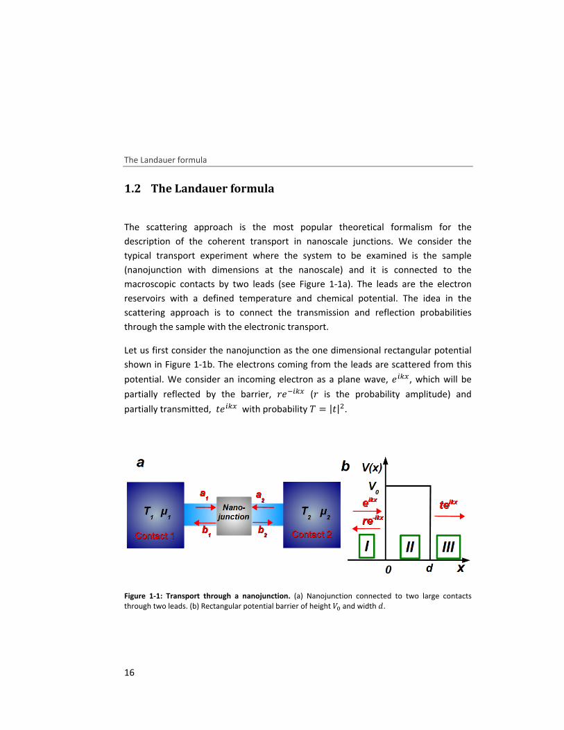
The Landauer formula
16
1.2 The Landauer formula
The scattering approach is the most popular theoretical formalism for the
description of the coherent transport in nanoscale junctions. We consider the
typical transport experiment where the system to be examined is the sample
(nanojunction with dimensions at the nanoscale) and it is connected to the
macroscopic contacts by two leads (see Figure 1-1a). The leads are the electron
reservoirs with a defined temperature and chemical potential. The idea in the
scattering approach is to connect the transmission and reflection probabilities
through the sample with the electronic transport.
Let us first consider the nanojunction as the one dimensional rectangular potential
shown in Figure 1-1b. The electrons coming from the leads are scattered from this
potential. We consider an incoming electron as a plane wave, ���, which will be
partially reflected by the barrier, ����� (� is the probability amplitude) and
partially transmitted, ���� with probability � = |�|�.
Figure 1-1: Transport through a nanojunction. (a) Nanojunction connected to two large contacts through two leads. (b) Rectangular potential barrier of height � and width �.
Chapter 1: Quantum Electron Transport
17
The electrical density carried by an electron is given by the quantum mechanical
expression:
where !(") = ℏ" $⁄ is the group velocity, � is the length of the system.
For the system we examine, many electrons are participating in the transport so
that we have to consider a sum over " and take into account the Pauli principle by
introducing a factor &'(")(1 − &�(")), where &',� are the Fermi distributions in
reservoir 1 and 2. This factor will ensure that the initial occupied states of reservoir
1 and the empty states of reservoir 2 are contributing to the current flow from 1 to
2 which will be given by:
By converting the sum to an integral and changing variable " to + by introducing
the density of states �" �+⁄ = $ ℏ�"⁄ , we get:
In the same way, the current from reservoir 2 to 1 is given by
and the total current is
This is the Landauer formula and it illustrates the close relation between current
and transmission. An extra factor 2 is added because of the spin degeneracy. At
zero temperature, &'(+) and &�(+) are step functions and are equal to 1 below
,� = ℏ2$- ./
∗(1) �/�1 − /(1) �/∗
�1 2 = � !(")�("), Equation 1-2
,'→� = �4!(")�(")
�&'(")(1 − &�(")). Equation 1-3
,'→� = ℎ6�+�(+) &'(+)(1 − &�(+)). Equation 1-4
,�→' = ℎ6�+�(+) &�(+)(1 − &'(+)), Equation 1-5
(�) = ,'→� − ,�→' = 2ℎ 6�+�(+) (&'(+) − &�(+)). Equation 1-6
The Landauer formula
18
their chemical potentials 7' = +8 + � 2⁄ and 7� = +8 − � 2⁄ respectively, and 0
above this energy. The net current then for low voltages is = �� and the
conductance is given by:
For one single-mode conductor the conductance is given by the universal quantity � = 2� ℎ⁄ ≈ 12.9KΩ .
Let us now go back to the general two-lead scattering problem (Figure 1-1a) in
order to extract the multichannel Landauer formula. The reservoirs 1 and 2 have
temperatures �',�, chemical potentials 7',� and the distribution of the electrons
inside them is described by the Fermi distribution. We assume that far from the
sample the transverse (perpendicular to the direction of transport) and the
longitudinal (along the direction of transport) motion of the electrons can be
separated. In the longitudinal direction the system is open, and is characterized by a
continuous wavevector "= and a longitudinal energy += = ℏ�"=�/2$. The
transverse motion is quantized and described by a discrete index ? and the
transverse energies +',�;A. These states are called quantum channels. The total
energy is + = +A + += , and since += is positive, for a given total energy, +, only
finite number of channels exist. �B',� and CD',� (see Figure 1-1a) are the operators
describing the incoming electrons impinging on the sample and the outgoing
respectively, and they are related through the scattering matrix �E:
where the blocks � and �G describe the electron reflection back to the resevoirs 1,2
and the blocks � and �G the electron transmission through the sample.
The Landauer formula can be generalized to multiple transverse energies, by
introducing the matrix ��H which can be extracted with simple matrix algebra from
the scattering matrix.�A(+) are its eigenvalues (transmission coefficients) with
values 0 < �A(+) < 1. The corresponding wavefunctions are referred as
� = 2�ℎ �. Equation 1-7
�E = K� �G� �GL, Equation 1-8
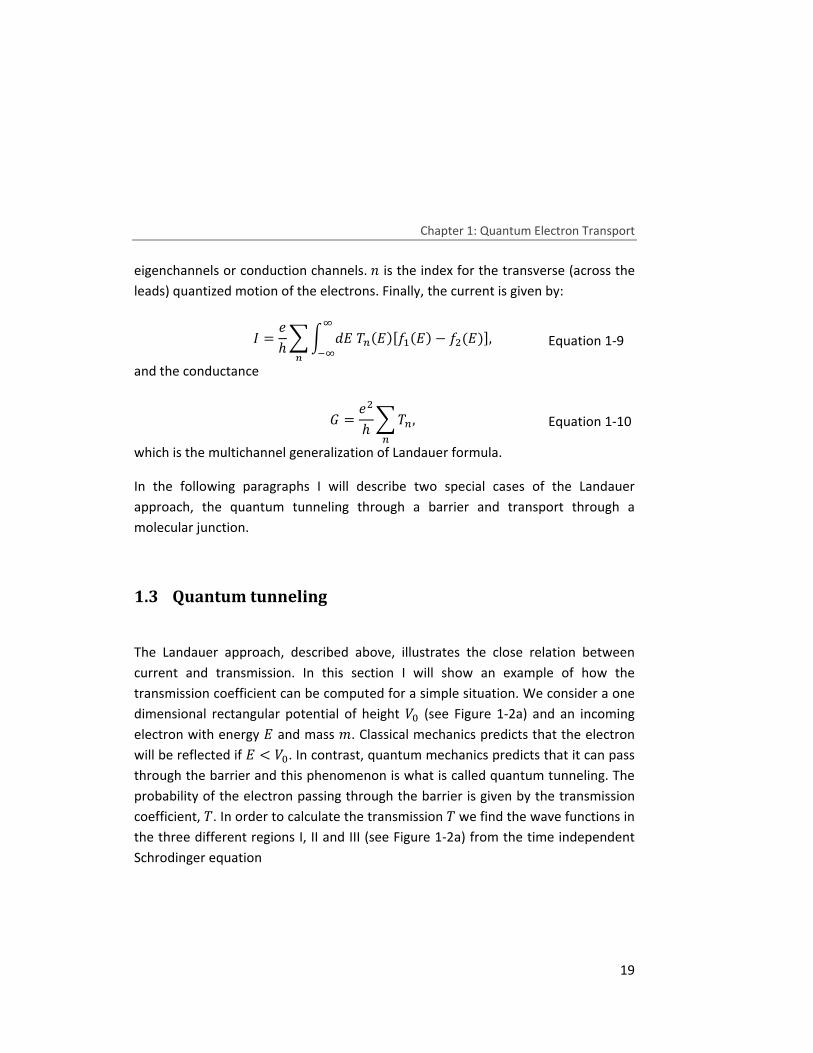
Chapter 1: Quantum Electron Transport
19
eigenchannels or conduction channels.? is the index for the transverse (across the
leads) quantized motion of the electrons. Finally, the current is given by:
and the conductance
which is the multichannel generalization of Landauer formula.
In the following paragraphs I will describe two special cases of the Landauer
approach, the quantum tunneling through a barrier and transport through a
molecular junction.
1.3 Quantum tunneling
The Landauer approach, described above, illustrates the close relation between
current and transmission. In this section I will show an example of how the
transmission coefficient can be computed for a simple situation. We consider a one
dimensional rectangular potential of height � (see Figure 1-2a) and an incoming
electron with energy + and mass $. Classical mechanics predicts that the electron
will be reflected if + < � . In contrast, quantum mechanics predicts that it can pass
through the barrier and this phenomenon is what is called quantum tunneling. The
probability of the electron passing through the barrier is given by the transmission
coefficient, �. In order to calculate the transmission �we find the wave functions in
the three different regions I, II and III (see Figure 1-2a) from the time independent
Schrodinger equation
= ℎ46 �+�A(+)(&'(+) − &�(+))M�MA , Equation 1-9
� = �ℎ 4�AA , Equation 1-10
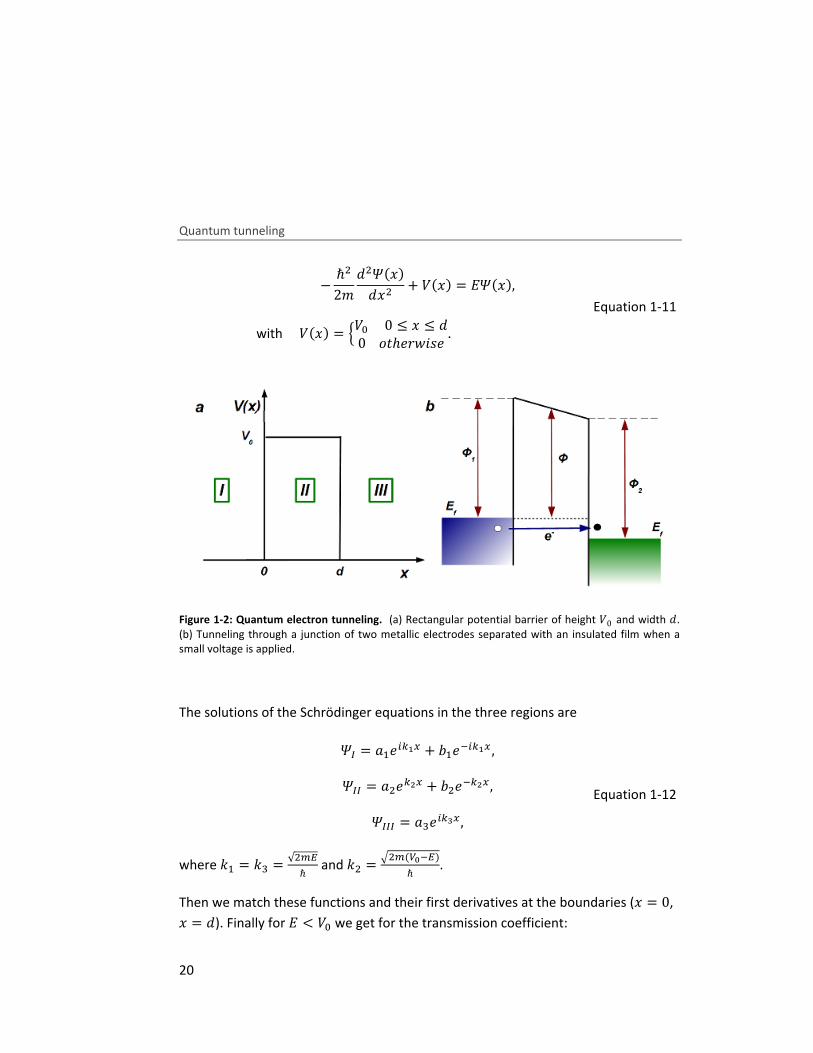
Quantum tunneling
20
Figure 1-2: Quantum electron tunneling. (a) Rectangular potential barrier of height �0 and width �. (b) Tunneling through a junction of two metallic electrodes separated with an insulated film when a small voltage is applied.
The solutions of the Schrödinger equations in the three regions are
where "' = "N = √�PQℏ and "� = R�P(ST�Q)ℏ .
Then we match these functions and their first derivatives at the boundaries (1 = 0, 1 = �). Finally for + < � we get for the transmission coefficient:
− ℏ�2$��/(1)�1� + �(1) = +/(1),
with �(1) = U� 0 ≤ 1 ≤ �0W�ℎ�X-Y . Equation 1-11
/Z = �'��[� + C'���[� , /ZZ = ���\� + C���\� ,
/ZZZ = �N��]� ,
Equation 1-12

Chapter 1: Quantum Electron Transport
21
When a voltage is applied a small drop appears in the potential profile (see Figure
1-2b). According to the calculations of Simmons, for a very small voltage the net
current density is a linear function of the applied voltage � and is given by:
where � = �ℏ√2$ [Binnig1982].
This formula gives an explanation for the exponential decay of the low bias
conductance. It has a strong exponential dependence on the barrier width � and
the effective barrier height (work function) ^ = � − +, which depends on the
material and the experimental conditions.
1.4 Quantum transport through molecular junctions
Another special case of the Landauer approach is transport through a molecular
junction connected to the macroscopic contacts by two leads (see Figure 1-3). In the
low voltage regime the transport mechanism through a molecule is mainly
tunneling and can be described with the scattering approach. We consider the level
scheme of Figure 1-3a, where molecular orbitals are within the junction and they
are occupied up to the highest occupied molecular orbital (HOMO). The Fermi
energy of the metallic leads is between the HOMO-LUMO (lowest unoccupied
molecular orbital) gap of the molecule. The molecular orbitals are broadened
depending on the metal-molecule coupling and many molecular orbitals can
participate in the transport.
However, a simplified model for transport, the “single-level resonant tunneling
model”, considers that the main participant is the closest to the Fermi energy.
Having this in mind, we can draw the schematic in Figure 1-3b. The main
� = _�N�'_� = `. ���\a . Equation 1-13
∝ `�cRda , Equation 1-14
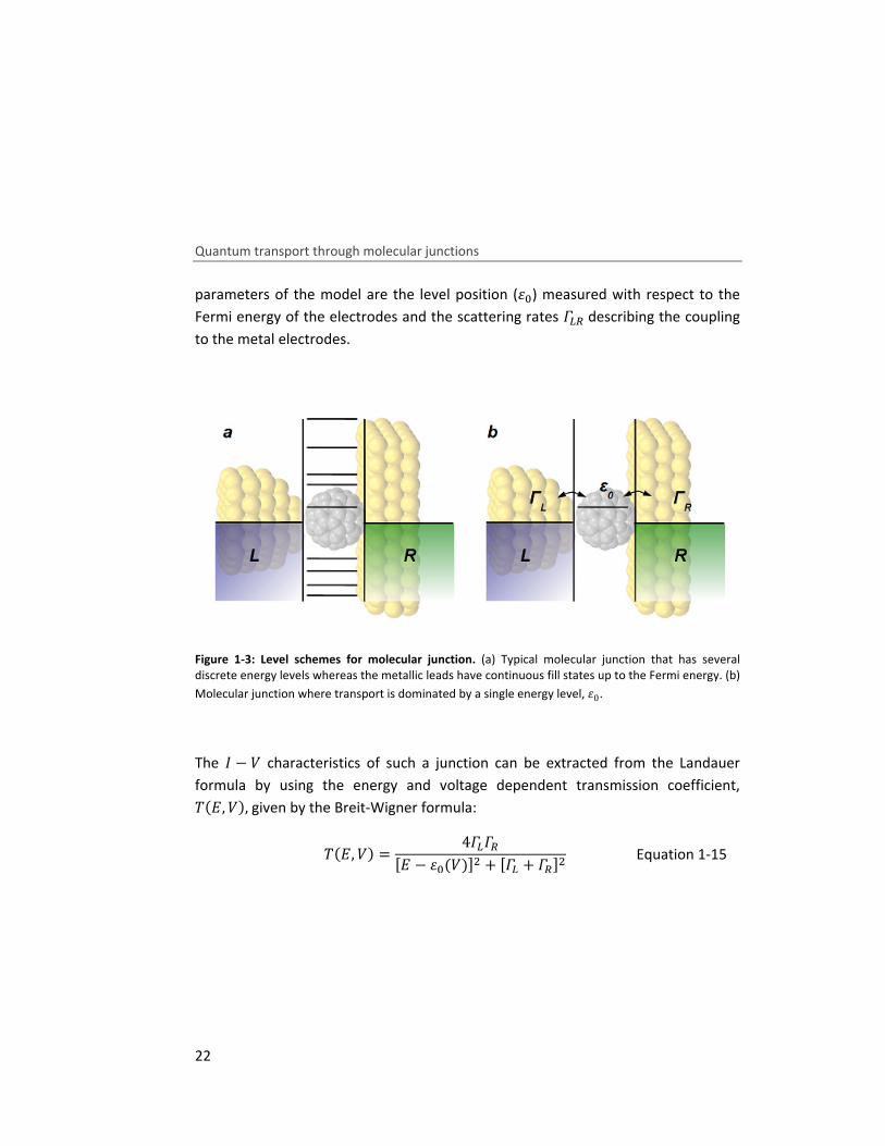
Quantum transport through molecular junctions
22
parameters of the model are the level position (e ) measured with respect to the
Fermi energy of the electrodes and the scattering rates fgh describing the coupling
to the metal electrodes.
Figure 1-3: Level schemes for molecular junction. (a) Typical molecular junction that has several discrete energy levels whereas the metallic leads have continuous fill states up to the Fermi energy. (b)
Molecular junction where transport is dominated by a single energy level, e0.
The − � characteristics of such a junction can be extracted from the Landauer
formula by using the energy and voltage dependent transmission coefficient, �(+, �), given by the Breit-Wigner formula:
�(+, �) = 4fgfh(+ − e (�))� + (fg + fh)� Equation 1-15
Chapter 1: Quantum Electron Transport
23
References
[Binnig1982] Binnig, G., H. Rohrer, C. Gerber and E. Weibel (1982). "Surface Studies
by Scanning Tunneling Microscopy." Physical Review Letters 49(1): 57-61. [Cuevas2010] Cuevas, J. C. and E. Scheer (2010). Molecular Electronics: An
Introduction to Theory and Experiment, World Scientific.

Thermoelectric effects are due to the coupling of thermal
In this chapter I will focus on the theory of one particular thermoelectric effect, the
Seebeck effect or thermopower. In the atomic scale the Seebeck effect is governed
by quantum effects that are radically different from the me
thermopower
classical theory of the Seebeck effect and then I will continue with the theory of
thermopower at the nanoscale. The scattering approach used in the p
chapter to describe the electronic transport is used here to describe quantum
thermoelectric effects.
2.1
In many metals and semiconductors there is a coupling between the electrical
current and the thermal current, which give
[Dresselhaus2001
thermoelectric devices
Seebeck effect
Seebeck effect
metallic bar is subjected to a voltage
current will be generated. The electric current
Thermoelectric effects are due to the coupling of thermal
In this chapter I will focus on the theory of one particular thermoelectric effect, the
Seebeck effect or thermopower. In the atomic scale the Seebeck effect is governed
by quantum effects that are radically different from the me
thermopower in macroscopic systems. I will first introduce all the definitions for the
classical theory of the Seebeck effect and then I will continue with the theory of
thermopower at the nanoscale. The scattering approach used in the p
chapter to describe the electronic transport is used here to describe quantum
thermoelectric effects.
2.1 Thermoelectric effect
In many metals and semiconductors there is a coupling between the electrical
current and the thermal current, which give
Dresselhaus2001
thermoelectric devices
Seebeck effect
Seebeck effect is the conversion of a temperature difference to electricity.
metallic bar is subjected to a voltage
current will be generated. The electric current
Thermoelectric effects are due to the coupling of thermal
In this chapter I will focus on the theory of one particular thermoelectric effect, the
Seebeck effect or thermopower. In the atomic scale the Seebeck effect is governed
by quantum effects that are radically different from the me
in macroscopic systems. I will first introduce all the definitions for the
classical theory of the Seebeck effect and then I will continue with the theory of
thermopower at the nanoscale. The scattering approach used in the p
chapter to describe the electronic transport is used here to describe quantum
thermoelectric effects.
Thermoelectric effect
In many metals and semiconductors there is a coupling between the electrical
current and the thermal current, which give
Dresselhaus2001]. There are three thermoelectric effects that ap
thermoelectric devices, the Seebeck effect
is the conversion of a temperature difference to electricity.
metallic bar is subjected to a voltage
current will be generated. The electric current
Thermoelectric effects are due to the coupling of thermal
In this chapter I will focus on the theory of one particular thermoelectric effect, the
Seebeck effect or thermopower. In the atomic scale the Seebeck effect is governed
by quantum effects that are radically different from the me
in macroscopic systems. I will first introduce all the definitions for the
classical theory of the Seebeck effect and then I will continue with the theory of
thermopower at the nanoscale. The scattering approach used in the p
chapter to describe the electronic transport is used here to describe quantum
Thermoelectric effect
In many metals and semiconductors there is a coupling between the electrical
current and the thermal current, which give
. There are three thermoelectric effects that ap
Seebeck effect
is the conversion of a temperature difference to electricity.
metallic bar is subjected to a voltage, �, or a temperature (
current will be generated. The electric current
Chapter
Thermoelectric effects are due to the coupling of thermal
In this chapter I will focus on the theory of one particular thermoelectric effect, the
Seebeck effect or thermopower. In the atomic scale the Seebeck effect is governed
by quantum effects that are radically different from the me
in macroscopic systems. I will first introduce all the definitions for the
classical theory of the Seebeck effect and then I will continue with the theory of
thermopower at the nanoscale. The scattering approach used in the p
chapter to describe the electronic transport is used here to describe quantum
In many metals and semiconductors there is a coupling between the electrical
current and the thermal current, which gives rise to thermoelectric phenomena
. There are three thermoelectric effects that ap
Seebeck effect, Peltier effect
is the conversion of a temperature difference to electricity.
or a temperature (
current will be generated. The electric current density,
Chapter 2: Thermoelectric Effects
Thermoelectric effects are due to the coupling of thermal and electrical transport.
In this chapter I will focus on the theory of one particular thermoelectric effect, the
Seebeck effect or thermopower. In the atomic scale the Seebeck effect is governed
by quantum effects that are radically different from the mechanisms governing
in macroscopic systems. I will first introduce all the definitions for the
classical theory of the Seebeck effect and then I will continue with the theory of
thermopower at the nanoscale. The scattering approach used in the p
chapter to describe the electronic transport is used here to describe quantum
In many metals and semiconductors there is a coupling between the electrical
s rise to thermoelectric phenomena
. There are three thermoelectric effects that ap
Peltier effect, and Thomson effec
is the conversion of a temperature difference to electricity.
or a temperature (�) difference an electric
density, ,, will be given by:
Thermoelectric Effects
and electrical transport.
In this chapter I will focus on the theory of one particular thermoelectric effect, the
Seebeck effect or thermopower. In the atomic scale the Seebeck effect is governed
chanisms governing
in macroscopic systems. I will first introduce all the definitions for the
classical theory of the Seebeck effect and then I will continue with the theory of
thermopower at the nanoscale. The scattering approach used in the previous
chapter to describe the electronic transport is used here to describe quantum
In many metals and semiconductors there is a coupling between the electrical
s rise to thermoelectric phenomena
. There are three thermoelectric effects that appear in
Thomson effect.
is the conversion of a temperature difference to electricity. When a
) difference an electric
given by:
Thermoelectric Effects
25
and electrical transport.
In this chapter I will focus on the theory of one particular thermoelectric effect, the
Seebeck effect or thermopower. In the atomic scale the Seebeck effect is governed
chanisms governing
in macroscopic systems. I will first introduce all the definitions for the
classical theory of the Seebeck effect and then I will continue with the theory of
revious
chapter to describe the electronic transport is used here to describe quantum
In many metals and semiconductors there is a coupling between the electrical
s rise to thermoelectric phenomena
pear in
When a
) difference an electric
Thermoelectric effect
26
where � is the conductivity and kl� is the voltage gradient. +lmn = −�kl� is the field
generated locally by the thermal electromotive force, where � is what called
Seebeck coefficient.
If the system reaches a steady state where , = 0 everywhere then
If the temperature difference (��) between the two ends of the material is small
then:
where ��is the thermoelectric voltage at the two ends.
Peltier effect
Peltier Effect is the heating or cooling effect created at a junction of two different
conductors A and B, when an electric current flows through the junction. Heating or
cooling depends on the direction of the current. The Peltier heat that is generated
at the junction per unit time is given by
where op and oq are the Peltier coefficients for conductor A and B respectively and
they represent how much heat is carried by a unit charge. is the current from A to
B.
The total heat at the junction can be influenced by Joule heating and thermal
gradient effects in addition to the Peltier heat.
Peltier and Seebeck effects are connected through the Thomson relation:
, = �(−kl� + +lmn), Equation 2-1
kl� = −�kl�, Equation 2-2
� = −���� Equation 2-3
rs = (op −oq) Equation 2-4
o = �� Equation 2-5
Chapter 2: Thermoelectric Effects
27
The above relation implies that in a close thermoelectric circuit the Seebeck effect
will drive a current which through the Peltier effect will transfer heat from the cold
to the hot junction.
Thomson effect:
Thomson effect is a reversible heating or cooling of a homogeneous conductor
when there is a flow of electric current and a temperature gradient. The Seebeck
coefficient of a material, usually is not constant with temperature thus if there is a
spatial temperature gradient in a material will cause a gradient in the Seebeck
coefficient. If a current pass through this gradient then a Peltier effect will occur.
For a current density , passing through a conductor the heat production rate per
unit volume is
where kl� is the temperature gradient and t the Thomson coefficient.
The Thomson coefficient is related with the Seebeck coefficient through the relation
2.2 The Seebeck effect
In this section the Seebeck effect is described in more detail, since this is the effect
we will study in this thesis. We can consider a metallic piece that is heated at one
end and cooled at the other (Figure 2-1). The electrons at the hot end are more
energetic and a diffusion of electrons from the hot end to the cold end will occur.
Positive carriers accumulate in the hot region and negative in the cold region. This
separation of the carriers produces an electric field and therefore a voltage
difference between the cold and hot ends. However there is always a competing
process. Some low energy electrons from the cold end will start diffusing in the
us = −t,kl� Equation 2-6
t = � ����. Equation 2-7
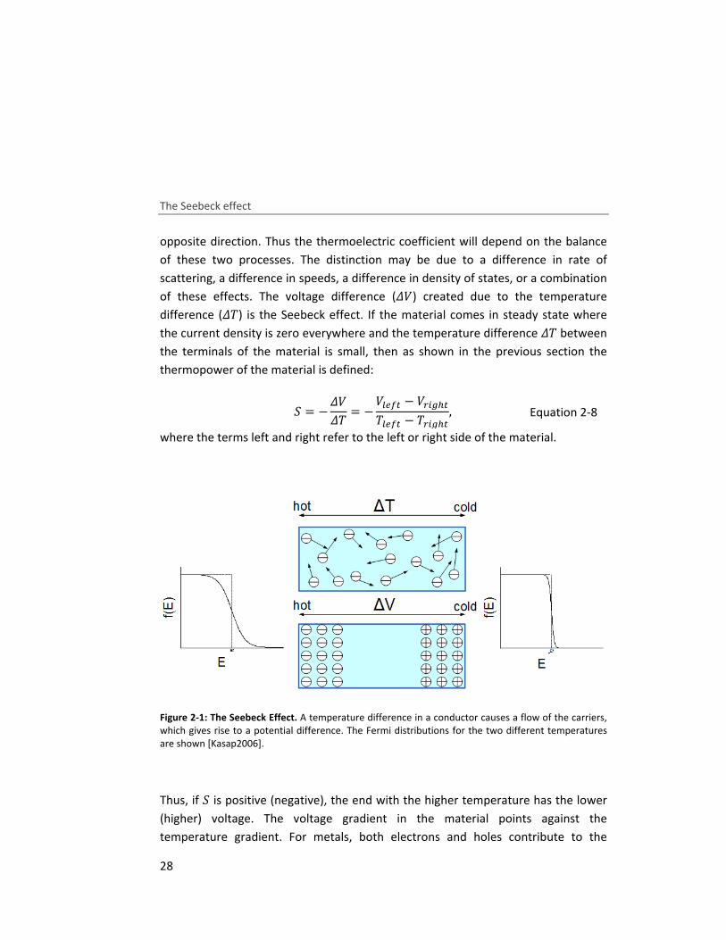
The Seebeck effect
28
opposite direction. Thus the thermoelectric coefficient will depend on the balance
of these two processes. The distinction may be due to a difference in rate of
scattering, a difference in speeds, a difference in density of states, or a combination
of these effects. The voltage difference (��) created due to the temperature
difference (��) is the Seebeck effect. If the material comes in steady state where
the current density is zero everywhere and the temperature difference �� between
the terminals of the material is small, then as shown in the previous section the
thermopower of the material is defined:
where the terms left and right refer to the left or right side of the material.
Figure 2-1: The Seebeck Effect. A temperature difference in a conductor causes a flow of the carriers, which gives rise to a potential difference. The Fermi distributions for the two different temperatures are shown [Kasap2006].
Thus, if � is positive (negative), the end with the higher temperature has the lower
(higher) voltage. The voltage gradient in the material points against the
temperature gradient. For metals, both electrons and holes contribute to the
� = −���� = −�=vwm − �x�ynm�=vwm − �x�ynm , Equation 2-8
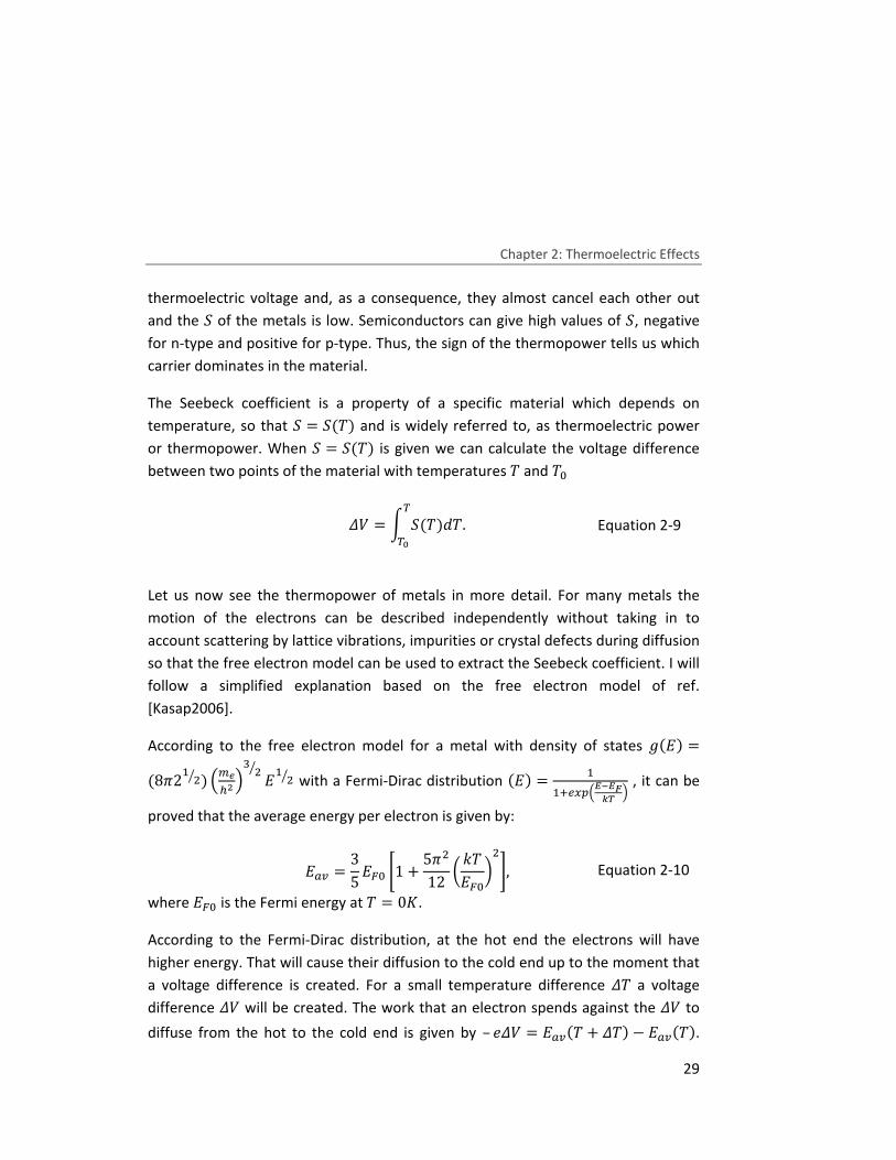
Chapter 2: Thermoelectric Effects
29
thermoelectric voltage and, as a consequence, they almost cancel each other out
and the � of the metals is low. Semiconductors can give high values of �, negative
for n-type and positive for p-type. Thus, the sign of the thermopower tells us which
carrier dominates in the material.
The Seebeck coefficient is a property of a specific material which depends on
temperature, so that � = �(�) and is widely referred to, as thermoelectric power
or thermopower. When � = �(�) is given we can calculate the voltage difference
between two points of the material with temperatures � and �
Let us now see the thermopower of metals in more detail. For many metals the
motion of the electrons can be described independently without taking in to
account scattering by lattice vibrations, impurities or crystal defects during diffusion
so that the free electron model can be used to extract the Seebeck coefficient. I will
follow a simplified explanation based on the free electron model of ref.
[Kasap2006].
According to the free electron model for a metal with density of states z(+) =(8|2' �� ) KP}n\LN �� +' �� with a Fermi-Dirac distribution (+) = ''~v��K������ L , it can be
proved that the average energy per electron is given by:
where +8 is the Fermi energy at � = 0�.
According to the Fermi-Dirac distribution, at the hot end the electrons will have
higher energy. That will cause their diffusion to the cold end up to the moment that
a voltage difference is created. For a small temperature difference �� a voltage
difference �� will be created. The work that an electron spends against the �� to
diffuse from the hot to the cold end is given by – �� = +��(� + ��) − +��(�).
�� = 6 �(�)����T . Equation 2-9
+�� = 35+8 �1 + 5|�12 �"�+8 ���, Equation 2-10
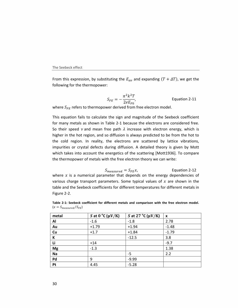
The Seebeck effect
30
From this expression, by substituting the +�� and expanding (� + ��), we get the
following for the thermopower:
where �8Q refers to thermopower derived from free electron model.
This equation fails to calculate the sign and magnitude of the Seebeck coefficient
for many metals as shown in Table 2-1 because the electrons are considered free.
So their speed �and mean free path � increase with electron energy, which is
higher in the hot region, and so diffusion is always predicted to be from the hot to
the cold region. In reality, the electrons are scattered by lattice vibrations,
impurities or crystal defects during diffusion. A detailed theory is given by Mott
which takes into account the energetics of the scattering [Mott1936]. To compare
the thermopower of metals with the free electron theory we can write:
where 1 is a numerical parameter that depends on the energy dependencies of
various charge transport parameters. Some typical values of 1 are shown in the
table and the Seebeck coefficients for different temperatures for different metals in
Figure 2-2.
Table 2-1: Seebeck coefficient for different metals and comparison with the free electron model.
(1 = �Pv���xva �8Q⁄ )
metal � at � oC (��/�) � at ��
oC (��/�) x
Al -1.6 -1.8 2.78
Au +1.79 +1.94 -1.48
Cu +1.7 +1.84 -1.79
K -12.5 3.8
Li +14 -9.7
Mg -1.3 1.38
Na -5 2.2
Pd 9 -9.99
Pt 4.45 -5.28
�8Q = −|�"��2+8 , Equation 2-11
�Pv���xva = �8Q1, Equation 2-12
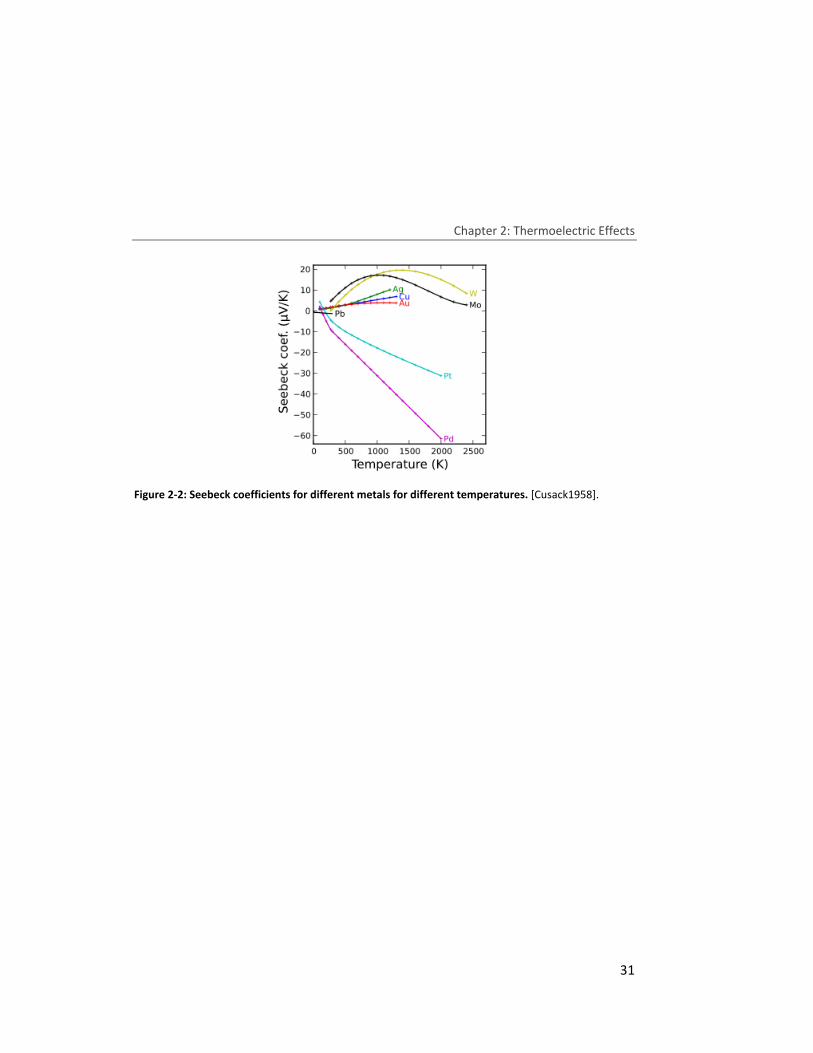
Chapter 2: Thermoelectric Effects
31
Figure 2-2: Seebeck coefficients for different metals for different temperatures. [Cusack1958].
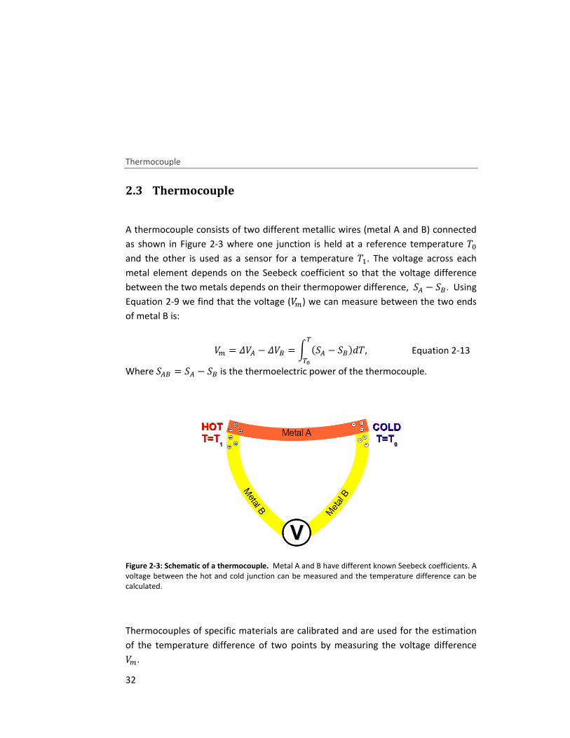
Thermocouple
32
2.3 Thermocouple
A thermocouple consists of two different metallic wires (metal A and B) connected
as shown in Figure 2-3 where one junction is held at a reference temperature �
and the other is used as a sensor for a temperature �'. The voltage across each
metal element depends on the Seebeck coefficient so that the voltage difference
between the two metals depends on their thermopower difference, �p − �q. Using
Equation 2-9 we find that the voltage (�P) we can measure between the two ends
of metal B is:
Where �pq = �p − �q is the thermoelectric power of the thermocouple.
Figure 2-3: Schematic of a thermocouple. Metal A and B have different known Seebeck coefficients. A voltage between the hot and cold junction can be measured and the temperature difference can be calculated.
Thermocouples of specific materials are calibrated and are used for the estimation
of the temperature difference of two points by measuring the voltage difference �P.
�P = ��p − ��q = 6 (�p − �q)����T , Equation 2-13
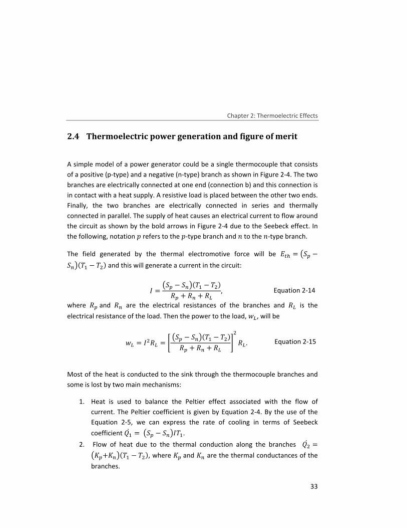
Chapter 2: Thermoelectric Effects
33
2.4 Thermoelectric power generation and figure of merit
A simple model of a power generator could be a single thermocouple that consists
of a positive (p-type) and a negative (n-type) branch as shown in Figure 2-4. The two
branches are electrically connected at one end (connection b) and this connection is
in contact with a heat supply. A resistive load is placed between the other two ends.
Finally, the two branches are electrically connected in series and thermally
connected in parallel. The supply of heat causes an electrical current to flow around
the circuit as shown by the bold arrows in Figure 2-4 due to the Seebeck effect. In
the following, notation � refers to the �-type branch and ? to the ?-type branch.
The field generated by the thermal electromotive force will be +mn = ��� −�A�(�' − ��) and this will generate a current in the circuit:
where ��and �A are the electrical resistances of the branches and �g is the
electrical resistance of the load. Then the power to the load, Xg, will be
Most of the heat is conducted to the sink through the thermocouple branches and
some is lost by two main mechanisms:
1. Heat is used to balance the Peltier effect associated with the flow of
current. The Peltier coefficient is given by Equation 2-4. By the use of the
Equation 2-5, we can express the rate of cooling in terms of Seebeck
coefficient r's = ��� − �A��'.
2. Flow of heat due to the thermal conduction along the branches r�s =���+�A�(�' − ��), where ��and �A are the thermal conductances of the
branches.
= ��� − �A�(�' − ��)�� + �A + �g , Equation 2-14
Xg = ��g = ���� − �A�(�' − ��)�� + �A + �g �� �g . Equation 2-15
Thermoelectric power generation and figure of merit
34
Then the total heat flow (rs ) from the source is
Figure 2-4: Thermoelectric Generator. A thermocouple used as a thermoelectric generator. Bold arrows show the direction of the generated current in the circuit and small arrows show the motion of the carriers due to the temperature difference in the material. Letters a-e indicate the different parts of the generator. [Winkless2012].
The efficiency is given by the relation � = Xg rs⁄ . The maximum efficiency can be
obtained by maximizing � with respect to �g. It can be shown that ? is maximum,
when the ratio of the load resistance, �g, to the internal resistance, �� + �A, is
given by:
where �P = �[~�\� and is the figure of merit which is given by:
rs = r's + r�s = ��� − �A��' + ���+�A�(�' − ��). Equation 2-16
�g�� + �A = R1 + �P, Equation 2-17
= ���� , Equation 2-18
Chapter 2: Thermoelectric Effects
35
where � = �� − �A is the thermopower, � = ��+�A is the thermal conductance
(notice that the branches are thermally connected in parallel) and � = 1 ���+�A�⁄
is the electrical conductance (notice that the branches are electrically connected in
series) of the thermocouple. has dimensions of inverse temperature. It can also
be expressed dimensionless as � at a specific temperature.
The efficiency will be
The efficiency ? increases by increasing the . In order to increase the the
quantity ���+�A����+�A�, that depends on the electrical resistance and thermal
conductance of the material, should minimized [Goldsmid2009; Rowe2010].
Equation 2-18 implies that an efficient thermoelectric device should maximize the
electrical conductance (minimize its internal resistance) and minimize the thermal
conductance simultaneously so that temperature gradient will be maintained in the
device. Finally, Seebeck coefficient should be maximized to ensure that coupling
between thermal and electrical current is as large as possible [Bergfield2013].
In generally the figure of merit of a thermoelectric material for a specific
temperature (�) is written as
where � is the thermal conductance and �the electrical conductance and � the
absolute thermopower of the material. � has an electrons and holes contribution
(�v=) and a phonons contribution �v=, so that � = �v= + ��n.
Increasing the figure of merit for a material by Increasing the electrical conductance
or decreasing the thermal conductance is difficult since, in most cases, the
Wiedemann-Franz law is valid, which indicates that, for a metal, the ratio of the
electronic contribution of the thermal conductance to the electrical conductance is
proportional to the temperature:
� = (�' − ��)�R1 + �P − 1��'�R1 + �P + �� �'⁄ � . Equation 2-19
� = ����� , Equation 2-20
Thermopower at the nanoscale
36
where � is the Lorentz number and it is equal to � = 2.44 × 10�¢WΩK��. With
any increase of the electrical conductance an increase of the thermal conductance
will appear. The approach to increase the figure of merit for a thermoelectric
material has been to maximize � and minimize ��n.
For practical applications, � > 1 is needed. A thermoelectric material with � > 4
would be the solution for many heating and cooling problems at the nano- and
macro- scale, with no operational carbon footprint. The best thermoelectric
materials up to now in the laboratory have � ≈ 3, while thermoelectric devices for
commercial use have � ≈ 1 due to various packaging and manufacturing
challenges [Bergfield2010].
2.5 Thermopower at the nanoscale
Thermopower at the nanoscale changes dramatically and quantum mechanics is
needed to describe the phenomena. In the following I describe the quantum
mechanical approach for the thermopower at the nanoscale.
2.5.1 Thermopower of a nanojunction
The thermopower at the nanoscale can be described, in the same way as we
described electronic transport, with the scattering approach. When a temperature
difference is applied at the two ends of a macroscopic material, a continuous
temperature gradient will be created in the material, while for a constriction
between two leads, a sharp drop of the temperature will be created at the point of
the constriction (see Figure 2-5). The electrons will be more energetic due to the
temperature and the transport of electrons trough the constriction to the cold lead
will start. Charges will start accumulating in one side of the constriction and leave
¥}¦§ = ��, Equation 2-21
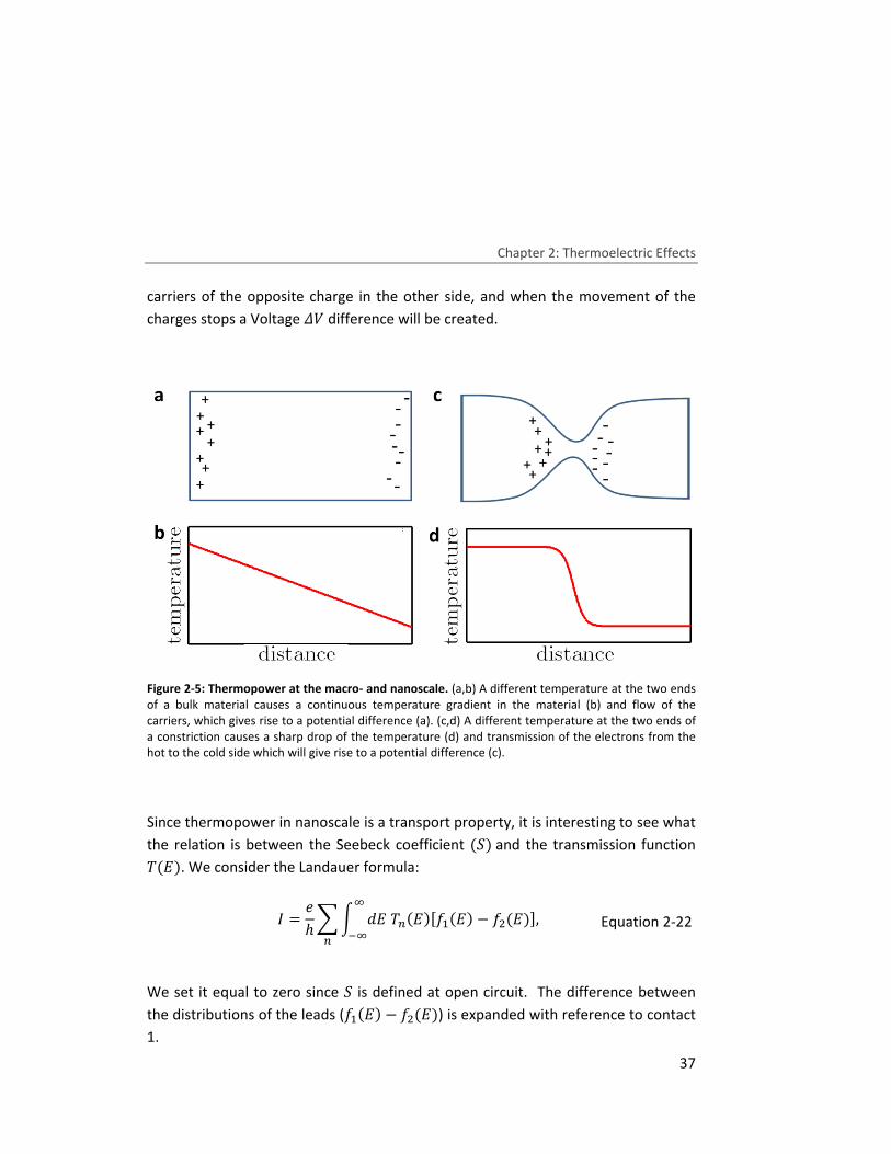
Chapter 2: Thermoelectric Effects
37
carriers of the opposite charge in the other side, and when the movement of the
charges stops a Voltage �� difference will be created.
Figure 2-5: Thermopower at the macro- and nanoscale. (a,b) A different temperature at the two ends of a bulk material causes a continuous temperature gradient in the material (b) and flow of the carriers, which gives rise to a potential difference (a). (c,d) A different temperature at the two ends of a constriction causes a sharp drop of the temperature (d) and transmission of the electrons from the hot to the cold side which will give rise to a potential difference (c).
Since thermopower in nanoscale is a transport property, it is interesting to see what
the relation is between the Seebeck coefficient (�)and the transmission function �(+). We consider the Landauer formula:
We set it equal to zero since � is defined at open circuit. The difference between
the distributions of the leads (&'(+) − &�(+)) is expanded with reference to contact
1.
= ℎ46 �+�A(+)(&'(+) − &�(+))M�MA , Equation 2-22
Thermopower at the nanoscale
38
The temperature derivative is written in terms of energy ¨w¨� = − Q�©ª ¨w¨« and the
chemical potential is approximated ¨w¨© = − ¨w¨Q ≈ ¬(+ − 7). Then from Equation
2-23 we get:
The change in chemical potential will cause a voltage �7'�� = −�'��. Then we
can Taylor expand the transmission function �(+) = �(+)|Q©[ + (® −7') ¨�(Q)¨« ¯Q©[and using the Summerfield expansion [Ashcroft1976] we get.
As indicated by the Equation 2-25, the thermopower is related to the transmission
function at the chemical potential of the contacts [Malen2010]. This formula is valid
at low temperatures and away from transition resonances so that the variation of
the transmission function is small [Dubi2011].
Thermal and electrical properties of a nanojunction can be written starting with the
fundamental thermodynamic identity at constant volume (��� = �+ − 7�°) and
using the measurable thermoelectric coefficients: electrical conductance �,
thermopower �, Peltier coefficient o and thermal conductance ±.
0 = 2ℎ 6 �+�(+) ²³´&´7_©©[µª[ �7'��M�M
+ ³´&´�_��[µ©[ ��'��¶ . Equation 2-23
�7'���·'�� = 1�(+)|Q©[ 6 �+�(+) ® − 7'·'
M�M
´&'´® . Equation 2-24
� = �'���·'�� = −|�"q��3 ´( ?�(+))´® ¸Q© . Equation 2-25
Chapter 2: Thermoelectric Effects
39
Equation 2-26 relates the charge current and the heat current rs with the electrical
bias ��and the temperature difference �� across the system. Furthermore, the
thermoelectric coefficients �, �, ± and � can be calculated by extending the
Landauer-Buttiker formalism to include both charge and heat currents in the linear
temperature and bias regime. [Bergfield2009; Finch2009]
where
In nanojunctions, in linear response and at room temperature the heat current is
carried mainly by electrons. For that reason usually the heat conductance ("�n) due
to phonons is neglected in the calculations and " = "v= [Bergfield2010].
The high correlation of the transport of heat and current, which is higher at the
nanoscale, makes the increase of the � very difficult. Although, due to the
coherent nature of the transport in the molecular junctions systems, quantum
interference phenomena could appear and give a large �.
���rs � = K� �o ±L K ��L. Equation 2-26
� = − 1� �'� , Equation 2-27
� = 2�ℎ � , Equation 2-28
± = −2ℎ 1� ³�� − �'�� µ, Equation 2-29
� = 1� ���'� − 1, Equation 2-30
�A = 6 �+ − +w���(+)M�M
´&(+)´+ �+. Equation 2-31
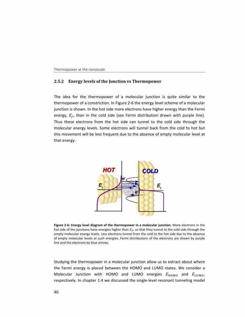
Thermopower at the nanoscale
40
2.5.2 Energy levels of the Junction vs Thermopower
The idea for the thermopower of a molecular junction is quite similar to the
thermopower of a constriction. In Figure 2-6 the energy level scheme of a molecular
junction is shown. In the hot side more electrons have higher energy than the Fermi
energy, +w, than in the cold side (see Fermi distribution drawn with purple line).
Thus these electrons from the hot side can tunnel to the cold side through the
molecular energy levels. Some electrons will tunnel back from the cold to hot but
this movement will be less frequent due to the absence of empty molecular level at
that energy.
Figure 2-6: Energy level diagram of the thermopower in a molecular junction. More electrons in the hot side of the junctions have energies higher than +8, so that they tunnel to the cold side through the empty molecular energy levels. Less electrons tunnel from the cold to the hot side due to the absence of empty molecular levels at such energies. Fermi distributions of the electrons are shown by purple line and the electrons by blue arrows.
Studying the thermopower in a molecular junction allow us to extract about where
the Fermi energy is placed between the HOMO and LUMO states. We consider a
Molecular Junction with HOMO and LUMO energies +¹º»º and +g¼»º,
respectively. In chapter 1.4 we discussed the single-level resonant tunneling model
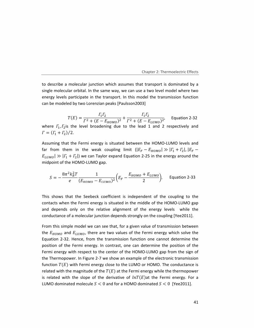
Chapter 2: Thermoelectric Effects
41
to describe a molecular junction which assumes that transport is dominated by a
single molecular orbital. In the same way, we can use a two level model where two
energy levels participate in the transport. In this model the transmission function
can be modeled by two Lorenzian peaks [Paulsson2003]
where f', f�is the level broadening due to the lead 1 and 2 respectively and f = (f' + f�) 2⁄ .
Assuming that the Fermi energy is situated between the HOMO-LUMO levels and
far from them in the weak coupling limit (|+8 − +¹º»º| ≫ |f' + f�|,|+8 −+g¼»º| ≫ |f' + f�|) we can Taylor expand Equation 2-25 in the energy around the
midpoint of the HOMO-LUMO gap.
This shows that the Seebeck coefficient is independent of the coupling to the
contacts when the Fermi energy is situated in the middle of the HOMO-LUMO gap
and depends only on the relative alignment of the energy levels while the
conductance of a molecular junction depends strongly on the coupling [Yee2011].
From this simple model we can see that, for a given value of transmission between
the +¹º»º and +g¼»º, there are two values of the Fermi energy which solve the
Equation 2-32. Hence, from the transmission function one cannot determine the
position of the Fermi energy. In contrast, one can determine the position of the
Fermi energy with respect to the center of the HOMO-LUMO gap from the sign of
the Thermopower. In Figure 2-7 we show an example of the electronic transmission
function �(+) with Fermi energy close to the LUMO or HOMO. The conductance is
related with the magnitude of the �(+) at the Fermi energy while the thermopower
is related with the slope of the derivative of ?�(+)at the Fermi energy. For a
LUMO dominated molecule � < 0 and for a HOMO dominated � < 0 [Yee2011].
�(+) = f'f�f� + (+ − +¹º»º)� + f'f�f� + (+ − +g¼»º)�, Equation 2-32
� = −8|�"q�� 1(+¹º»º − +g¼»º)� �+8 − +¹º»º + +g¼»º2 �. Equation 2-33
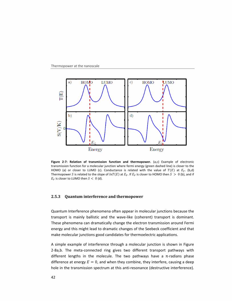
Thermopower at the nanoscale
42
Figure 2-7: Relation of transmission function and thermopower. (a,c) Example of electronic transmission function for a molecular junction where fermi energy (green dashed line) is closer to the HOMO (a) or closer to LUMO (c). Conductance is related with the value of �(+) at +8. (b,d) Thermopower � is related to the slope of ?�(+) at +8. If +8 is closer to HOMO then � > 0 (b), and if +8 is closer to LUMO then � < 0 (d).
2.5.3 Quantum interference and thermopower
Quantum Interference phenomena often appear in molecular junctions because the
transport is mainly ballistic and the wave-like (coherent) transport is dominant.
These phenomena can dramatically change the electron transmission around Fermi
energy and this might lead to dramatic changes of the Seebeck coefficient and that
make molecular junctions good candidates for thermoelectric applications.
A simple example of interference through a molecular junction is shown in Figure
2-8a,b. The meta-connected ring gives two different transport pathways with
different lengths in the molecule. The two pathways have a π-radians phase
difference at energy + = 0, and when they combine, they interfere, causing a deep
hole in the transmission spectrum at this anti-resonance (destructive interference).
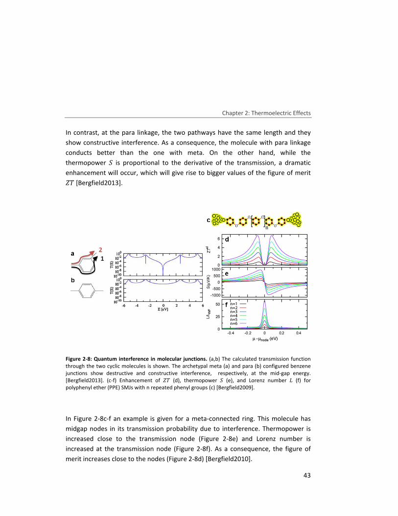
Chapter 2: Thermoelectric Effects
43
In contrast, at the para linkage, the two pathways have the same length and they
show constructive interference. As a consequence, the molecule with para linkage
conducts better than the one with meta. On the other hand, while the
thermopower � is proportional to the derivative of the transmission, a dramatic
enhancement will occur, which will give rise to bigger values of the figure of merit �[Bergfield2013].
Figure 2-8: Quantum interference in molecular junctions. (a,b) The calculated transmission function through the two cyclic molecules is shown. The archetypal meta (a) and para (b) configured benzene junctions show destructive and constructive interference, respectively, at the mid-gap energy. [Bergfield2013]. (c-f) Enhancement of � (d), thermopower � (e), and Lorenz number � (f) for polyphenyl ether (PPE) SMJs with n repeated phenyl groups (c) [Bergfield2009].
In Figure 2-8c-f an example is given for a meta-connected ring. This molecule has
midgap nodes in its transmission probability due to interference. Thermopower is
increased close to the transmission node (Figure 2-8e) and Lorenz number is
increased at the transmission node (Figure 2-8f). As a consequence, the figure of
merit increases close to the nodes (Figure 2-8d) [Bergfield2010].
References
44
References
[Ashcroft1976] Ashcroft, N. W. and N. D. Mermin (1976). Solid state physics,
Saunders College. [Bergfield2013] Bergfield, J. P. and M. A. Ratner (2013). "Forty years of molecular
electronics: Non-equilibrium heat and charge transport at the nanoscale." physica status solidi (b) 250(11): 2249-2266.
[Bergfield2010] Bergfield, J. P., M. A. Solis and C. A. Stafford (2010). "Giant Thermoelectric Effect from Transmission Supernodes." ACS Nano 4(9): 5314-5320.
[Bergfield2009] Bergfield, J. P. and C. A. Stafford (2009). "Thermoelectric Signatures of Coherent Transport in Single-Molecule Heterojunctions." Nano Letters 9(8): 3072-3076.
[Cusack1958] Cusack, N. and P. Kendall (1958). "The Absolute Scale of Thermoelectric Power at High Temperature." Proceedings of the Physical Society (1960) 72(5): 898-901.
[Dresselhaus2001] Dresselhaus, M. S. (2001). SOLID STATE PHYSICS Transport Properties of Solids.
[Dubi2011] Dubi, Y. and M. Di Ventra (2011). "Colloquium: Heat flow and thermoelectricity in atomic and molecular junctions." Reviews of Modern Physics 83(1): 131-155.
[Finch2009] Finch, C. M., V. M. García-Suárez and C. J. Lambert (2009). "Giant thermopower and figure of merit in single-molecule devices." Physical Review B 79(3): 033405.
[Goldsmid2009] Goldsmid, H. J. (2009). Introduction to Thermoelectricity, Springer. [Kasap2006] Kasap, S. O. (2006). Principles of Electronic Materials and Devices,
McGraw-Hill Education. [Malen2010] Malen, J. A., S. K. Yee, A. Majumdar and R. A. Segalman (2010).
"Fundamentals of energy transport, energy conversion, and thermal properties in organic–inorganic heterojunctions." Chemical Physics Letters 491(4–6): 109-122.
[Mott1936] Mott, N. F. and H. Jones (1936). The Theory of the Properties of Metals and Alloys, Clarendon Press.
[Paulsson2003] Paulsson, M. and S. Datta (2003). "Thermoelectric effect in molecular electronics." Physical Review B 67(24): 241403.
[Rowe2010] Rowe, D. M. (2010). CRC Handbook of Thermoelectrics, Taylor & Francis.
Chapter 2: Thermoelectric Effects
45
[Winkless2012] Winkless, L. (2012). "Thermoelectric Generators - TEGs." from http://www.thenakedscientists.com/HTML/articles/article/thermoelectric-generators/.
[Yee2011] Yee, S. K., J. A. Malen, A. Majumdar and R. A. Segalman (2011). "Thermoelectricity in Fullerene–Metal Heterojunctions." Nano Letters 11(10): 4089-4094.

In this chapter
used to obtain the r
STM) a
partially
3.1
The Scanning Tunneling Microscope (STM) was the experimental t
the big breakthrough in Nanotechnology in the last 30 years. In 1981 G.Binning,
H.Rohrer, Ch. Gerber and E. Weibel observed vacuum tunneling between a tungsten
tip and a platinum sample
of scanning using piezoelectric elements, generated the STM. In 1986 the first two
were awarded the Nobel Prize in Physics.
gives many possibilities of investigating physical phenome
surface structure of conducting and semiconducting materials can be scanned with
atomic resolution. In addition, the tip acts as a probe giving the opportunity to
explore physical properties of the materials at the atomic scale by
spectroscopic techniques.
The idea of the STM is quite simple and is based on the quantum tunneling effect. A
bias voltage is applied between a sharp tip and the sample. Both sample and tip
should be conducting or semiconducting. As the tip
In this chapter
used to obtain the r
STM) and the Low Temperature STM (LT STM). The two setups were modified and
partially re-built in order to adapt them for the desired experiments.
3.1 Functioning of
The Scanning Tunneling Microscope (STM) was the experimental t
the big breakthrough in Nanotechnology in the last 30 years. In 1981 G.Binning,
H.Rohrer, Ch. Gerber and E. Weibel observed vacuum tunneling between a tungsten
tip and a platinum sample
of scanning using piezoelectric elements, generated the STM. In 1986 the first two
were awarded the Nobel Prize in Physics.
gives many possibilities of investigating physical phenome
surface structure of conducting and semiconducting materials can be scanned with
atomic resolution. In addition, the tip acts as a probe giving the opportunity to
explore physical properties of the materials at the atomic scale by
spectroscopic techniques.
The idea of the STM is quite simple and is based on the quantum tunneling effect. A
bias voltage is applied between a sharp tip and the sample. Both sample and tip
should be conducting or semiconducting. As the tip
I will describe the two homebuilt Scanning Tunneling Microscopes
used to obtain the results presented in this thesis:
nd the Low Temperature STM (LT STM). The two setups were modified and
built in order to adapt them for the desired experiments.
Functioning of the
The Scanning Tunneling Microscope (STM) was the experimental t
the big breakthrough in Nanotechnology in the last 30 years. In 1981 G.Binning,
H.Rohrer, Ch. Gerber and E. Weibel observed vacuum tunneling between a tungsten
tip and a platinum sample [Binnig1982
of scanning using piezoelectric elements, generated the STM. In 1986 the first two
were awarded the Nobel Prize in Physics.
gives many possibilities of investigating physical phenome
surface structure of conducting and semiconducting materials can be scanned with
atomic resolution. In addition, the tip acts as a probe giving the opportunity to
explore physical properties of the materials at the atomic scale by
spectroscopic techniques.
The idea of the STM is quite simple and is based on the quantum tunneling effect. A
bias voltage is applied between a sharp tip and the sample. Both sample and tip
should be conducting or semiconducting. As the tip
describe the two homebuilt Scanning Tunneling Microscopes
esults presented in this thesis:
nd the Low Temperature STM (LT STM). The two setups were modified and
built in order to adapt them for the desired experiments.
the Scanning Tunneling Microscope
The Scanning Tunneling Microscope (STM) was the experimental t
the big breakthrough in Nanotechnology in the last 30 years. In 1981 G.Binning,
H.Rohrer, Ch. Gerber and E. Weibel observed vacuum tunneling between a tungsten
Binnig1982]. This obse
of scanning using piezoelectric elements, generated the STM. In 1986 the first two
were awarded the Nobel Prize in Physics.
gives many possibilities of investigating physical phenome
surface structure of conducting and semiconducting materials can be scanned with
atomic resolution. In addition, the tip acts as a probe giving the opportunity to
explore physical properties of the materials at the atomic scale by
The idea of the STM is quite simple and is based on the quantum tunneling effect. A
bias voltage is applied between a sharp tip and the sample. Both sample and tip
should be conducting or semiconducting. As the tip
describe the two homebuilt Scanning Tunneling Microscopes
esults presented in this thesis: the Room Temperature STM (RT
nd the Low Temperature STM (LT STM). The two setups were modified and
built in order to adapt them for the desired experiments.
Scanning Tunneling Microscope
The Scanning Tunneling Microscope (STM) was the experimental t
the big breakthrough in Nanotechnology in the last 30 years. In 1981 G.Binning,
H.Rohrer, Ch. Gerber and E. Weibel observed vacuum tunneling between a tungsten
. This observation, combined with the ability
of scanning using piezoelectric elements, generated the STM. In 1986 the first two
were awarded the Nobel Prize in Physics. The STM is a powerful instrument which
gives many possibilities of investigating physical phenome
surface structure of conducting and semiconducting materials can be scanned with
atomic resolution. In addition, the tip acts as a probe giving the opportunity to
explore physical properties of the materials at the atomic scale by
The idea of the STM is quite simple and is based on the quantum tunneling effect. A
bias voltage is applied between a sharp tip and the sample. Both sample and tip
should be conducting or semiconducting. As the tip
Chapter 3: Experimental Tools
describe the two homebuilt Scanning Tunneling Microscopes
the Room Temperature STM (RT
nd the Low Temperature STM (LT STM). The two setups were modified and
built in order to adapt them for the desired experiments.
Scanning Tunneling Microscope
The Scanning Tunneling Microscope (STM) was the experimental t
the big breakthrough in Nanotechnology in the last 30 years. In 1981 G.Binning,
H.Rohrer, Ch. Gerber and E. Weibel observed vacuum tunneling between a tungsten
rvation, combined with the ability
of scanning using piezoelectric elements, generated the STM. In 1986 the first two
STM is a powerful instrument which
gives many possibilities of investigating physical phenomena at the nanoscale. The
surface structure of conducting and semiconducting materials can be scanned with
atomic resolution. In addition, the tip acts as a probe giving the opportunity to
explore physical properties of the materials at the atomic scale by
The idea of the STM is quite simple and is based on the quantum tunneling effect. A
bias voltage is applied between a sharp tip and the sample. Both sample and tip
should be conducting or semiconducting. As the tip approaches the sample a
Experimental Tools
describe the two homebuilt Scanning Tunneling Microscopes
the Room Temperature STM (RT
nd the Low Temperature STM (LT STM). The two setups were modified and
built in order to adapt them for the desired experiments.
Scanning Tunneling Microscope
The Scanning Tunneling Microscope (STM) was the experimental tool that caused
the big breakthrough in Nanotechnology in the last 30 years. In 1981 G.Binning,
H.Rohrer, Ch. Gerber and E. Weibel observed vacuum tunneling between a tungsten
rvation, combined with the ability
of scanning using piezoelectric elements, generated the STM. In 1986 the first two
STM is a powerful instrument which
na at the nanoscale. The
surface structure of conducting and semiconducting materials can be scanned with
atomic resolution. In addition, the tip acts as a probe giving the opportunity to
explore physical properties of the materials at the atomic scale by using different
The idea of the STM is quite simple and is based on the quantum tunneling effect. A
bias voltage is applied between a sharp tip and the sample. Both sample and tip
approaches the sample a
Experimental Tools
47
describe the two homebuilt Scanning Tunneling Microscopes
the Room Temperature STM (RT
nd the Low Temperature STM (LT STM). The two setups were modified and
ool that caused
the big breakthrough in Nanotechnology in the last 30 years. In 1981 G.Binning,
H.Rohrer, Ch. Gerber and E. Weibel observed vacuum tunneling between a tungsten
rvation, combined with the ability
of scanning using piezoelectric elements, generated the STM. In 1986 the first two
STM is a powerful instrument which
na at the nanoscale. The
surface structure of conducting and semiconducting materials can be scanned with
atomic resolution. In addition, the tip acts as a probe giving the opportunity to
using different
The idea of the STM is quite simple and is based on the quantum tunneling effect. A
bias voltage is applied between a sharp tip and the sample. Both sample and tip
approaches the sample a

Functioning of the Scanning Tunneling Microscope
48
current flow appears between the apex of the tip and locally on the sample due to
the quantum tunneling effect.
Figure 3-1: The basic principle of STM function. A bias voltage is applied between the tip and the sample. The tip can move in the 1, ¾, ¿ direction and the distance between the tip and the sample is controlled by a feedback loop.
By keeping the tunneling current constant by means of a feedback loop, and
scanning the surface along the 1 and ¾ axes we can record the ¿ movement and
create a 3D local mapping of the surface (Figure 3-2a). The adjustment of the
vertical height is performed by applying voltage (�À) at the ¿ piezoelectric drive, and
the lateral tip position is determined by the voltages ��, �Á applied on the 1 and ¾
piezoelectric drive respectively. Finally, the recorded signal �À(��, �Á), can give the
topographic image ¿(1, ¾) if the calibration of the piezoelectric drive is known.
The feedback loop has a finite response which limits the speed of scanning in the
constant current mode. A way to avoid that is the constant height imaging (Figure
3-2b) where the feedback loop is switched off. The vertical tip/sample distance is
kept constant and the tunneling current is recorded while scanning in the 1, ¾
direction. The high sensitivity of the tunneling current, due to the exponential
dependence on the tip/surface distance, will give the topography of the surface
[Wiesendanger1994].
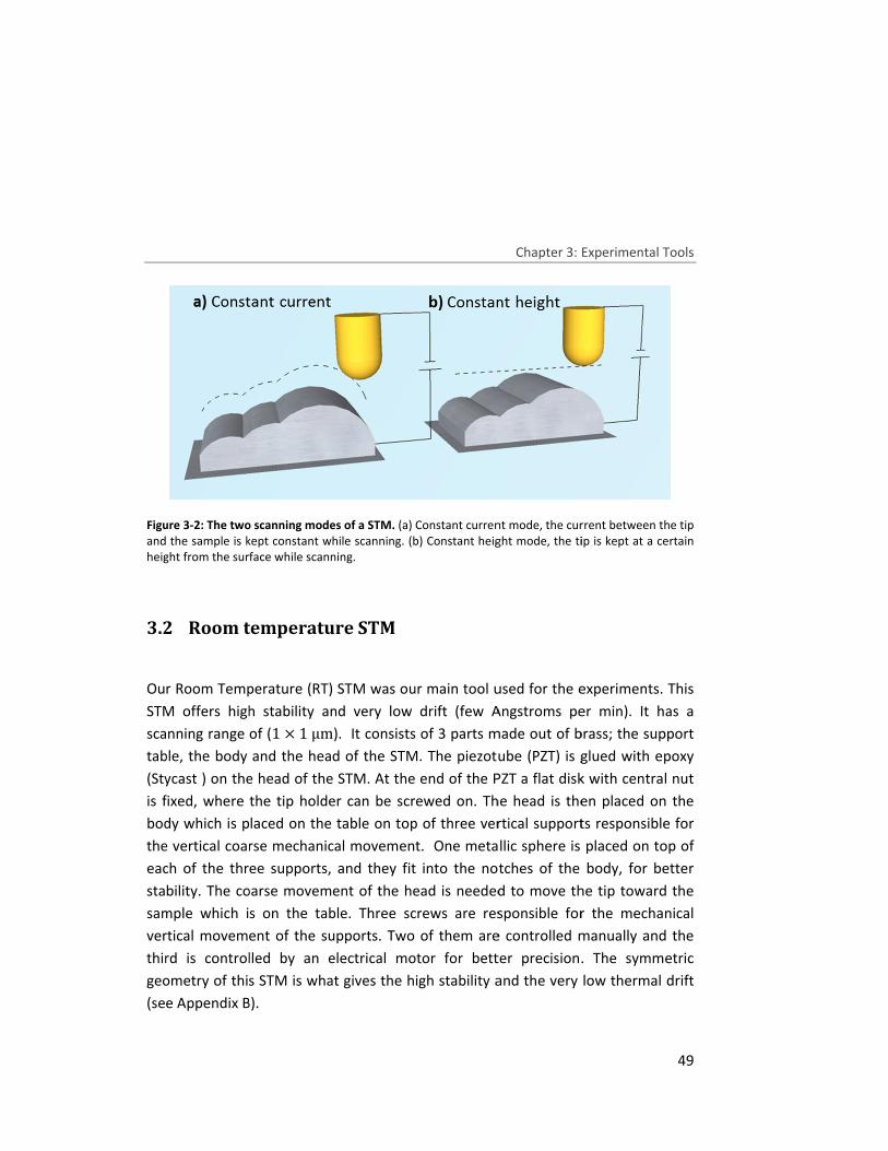
Figure
and the sample is kept constant while scanning. height from the surface while scanning.
3.2
Our
STM offers high stability and very low drift (
scanning range of (
table, the b
(Stycast ) on the head of the STM. At the end of the PZT a
is fixed, where the tip holder can be screwed on. The head is then placed on the
body which is placed
the vertical coarse mechanical movement. One metallic sphere is placed on top of
each of the three supports
stability. The coarse moveme
sample which is on the table. Three screws are responsible for the mechanical
vertical movement of the supports. Two of them are controlled manually and the
third is controlled by an electrical motor for
geometry
(see
Figure 3-2: The two
and the sample is kept constant while scanning. height from the surface while scanning.
3.2 Room t
Our Room Temperature (RT) STM
STM offers high stability and very low drift (
scanning range of (
table, the body and the head of the STM. The piezot
tycast ) on the head of the STM. At the end of the PZT a
is fixed, where the tip holder can be screwed on. The head is then placed on the
body which is placed
the vertical coarse mechanical movement. One metallic sphere is placed on top of
each of the three supports
stability. The coarse moveme
sample which is on the table. Three screws are responsible for the mechanical
vertical movement of the supports. Two of them are controlled manually and the
third is controlled by an electrical motor for
geometry of this STM is what gives the high stability and the very low thermal drift
see Appendix B
: The two scanning modes
and the sample is kept constant while scanning. height from the surface while scanning.
temperature ST
Room Temperature (RT) STM
STM offers high stability and very low drift (
scanning range of (1 ¡ 1μmody and the head of the STM. The piezot
tycast ) on the head of the STM. At the end of the PZT a
is fixed, where the tip holder can be screwed on. The head is then placed on the
body which is placed on the table on top of three vertical supports responsible for
the vertical coarse mechanical movement. One metallic sphere is placed on top of
each of the three supports, and the
stability. The coarse moveme
sample which is on the table. Three screws are responsible for the mechanical
vertical movement of the supports. Two of them are controlled manually and the
third is controlled by an electrical motor for
of this STM is what gives the high stability and the very low thermal drift
Appendix B).
scanning modes of a STM. (a) Constant current mode, the current between the tip and the sample is kept constant while scanning. (b)height from the surface while scanning.
emperature STM
Room Temperature (RT) STM was our main tool
STM offers high stability and very low drift (m). It consists of 3 parts made
ody and the head of the STM. The piezot
tycast ) on the head of the STM. At the end of the PZT a
is fixed, where the tip holder can be screwed on. The head is then placed on the
on the table on top of three vertical supports responsible for
the vertical coarse mechanical movement. One metallic sphere is placed on top of
, and they fit into the notches of the body,
stability. The coarse movement of the head is needed to move the tip toward the
sample which is on the table. Three screws are responsible for the mechanical
vertical movement of the supports. Two of them are controlled manually and the
third is controlled by an electrical motor for
of this STM is what gives the high stability and the very low thermal drift
Constant current mode, the current between the tip (b) Constant height mode, the tip is kept at a certain
our main tool used for the experiments. This
STM offers high stability and very low drift (few Angstroms per min
consists of 3 parts made
ody and the head of the STM. The piezotube (PZT) is glued with epoxy
tycast ) on the head of the STM. At the end of the PZT a
is fixed, where the tip holder can be screwed on. The head is then placed on the
on the table on top of three vertical supports responsible for
the vertical coarse mechanical movement. One metallic sphere is placed on top of
fit into the notches of the body,
nt of the head is needed to move the tip toward the
sample which is on the table. Three screws are responsible for the mechanical
vertical movement of the supports. Two of them are controlled manually and the
third is controlled by an electrical motor for better precision.
of this STM is what gives the high stability and the very low thermal drift
Chapter 3: Experimental Tools
Constant current mode, the current between the tip onstant height mode, the tip is kept at a certain
used for the experiments. This
few Angstroms per min
consists of 3 parts made out of brass; the support
ube (PZT) is glued with epoxy
tycast ) on the head of the STM. At the end of the PZT a flat disk with central
is fixed, where the tip holder can be screwed on. The head is then placed on the
on the table on top of three vertical supports responsible for
the vertical coarse mechanical movement. One metallic sphere is placed on top of
fit into the notches of the body,
nt of the head is needed to move the tip toward the
sample which is on the table. Three screws are responsible for the mechanical
vertical movement of the supports. Two of them are controlled manually and the
better precision.
of this STM is what gives the high stability and the very low thermal drift
Experimental Tools
Constant current mode, the current between the tip onstant height mode, the tip is kept at a certain
used for the experiments. This
few Angstroms per min). It has a
of brass; the support
ube (PZT) is glued with epoxy
flat disk with central
is fixed, where the tip holder can be screwed on. The head is then placed on the
on the table on top of three vertical supports responsible for
the vertical coarse mechanical movement. One metallic sphere is placed on top of
fit into the notches of the body, for better
nt of the head is needed to move the tip toward the
sample which is on the table. Three screws are responsible for the mechanical
vertical movement of the supports. Two of them are controlled manually and the
better precision. The symmetric
of this STM is what gives the high stability and the very low thermal drift
Experimental Tools
49
Constant current mode, the current between the tip onstant height mode, the tip is kept at a certain
used for the experiments. This
). It has a
of brass; the support
ube (PZT) is glued with epoxy
flat disk with central nut
is fixed, where the tip holder can be screwed on. The head is then placed on the
on the table on top of three vertical supports responsible for
the vertical coarse mechanical movement. One metallic sphere is placed on top of
for better
nt of the head is needed to move the tip toward the
sample which is on the table. Three screws are responsible for the mechanical
vertical movement of the supports. Two of them are controlled manually and the
The symmetric
of this STM is what gives the high stability and the very low thermal drift
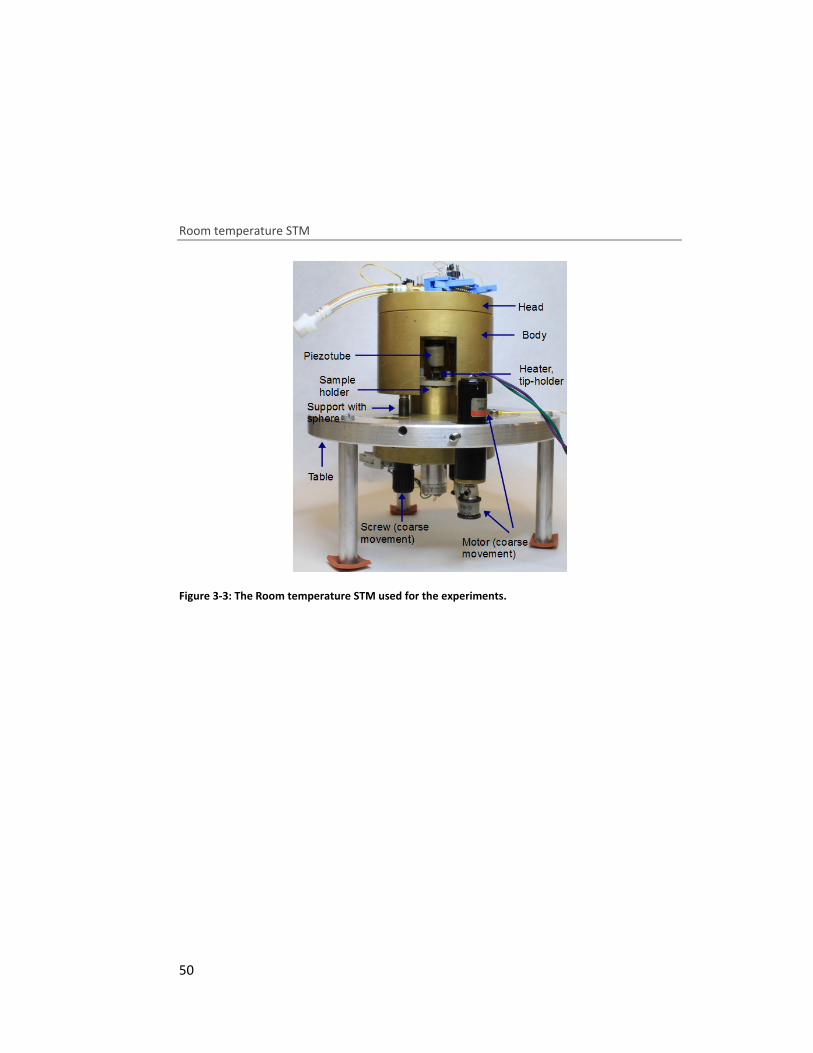
Room temperature STM
50
Figure 3-3: The Room temperature STM used for the experiments.
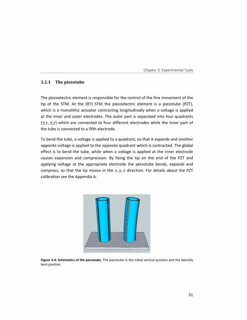
3.2.1
The piezoelectric element is responsible for the control of the fine movement of the
tip of the STM. At the
which is a monolithic actuator cont
at the inner and outer electrodes. The outer part is separated into four quadrants
(Ä1the tube is connected to a fifth electrode.
To bend the tube,
opposite
effect is to bend the tube,
causes expansion and compression.
applying voltage at the appropriate electrode
compress
calibration see the
Figure
bent position
3.2.1 The piezotube
The piezoelectric element is responsible for the control of the fine movement of the
tip of the STM. At the
which is a monolithic actuator cont
at the inner and outer electrodes. The outer part is separated into four quadrants 1, ľ) which are connected to four different electrodes while the inner part of
the tube is connected to a fifth electrode.
To bend the tube,
opposite voltage is
effect is to bend the tube,
causes expansion and compression.
applying voltage at the appropriate electrode
compress, so that
calibration see the
Figure 3-4: Schematics of the piezotube.
bent position.
piezotube
The piezoelectric element is responsible for the control of the fine movement of the
tip of the STM. At the (RT)
which is a monolithic actuator cont
at the inner and outer electrodes. The outer part is separated into four quadrants
) which are connected to four different electrodes while the inner part of
the tube is connected to a fifth electrode.
To bend the tube, a voltage is applied to a quadrant
voltage is applied to the opposite
effect is to bend the tube, while
causes expansion and compression.
applying voltage at the appropriate electrode
so that the tip moves
calibration see the Appendix A
Schematics of the piezotube.
The piezoelectric element is responsible for the control of the fine movement of the
) STM the piezoelectric element is a
which is a monolithic actuator contracting longitudinally when a voltage is applied
at the inner and outer electrodes. The outer part is separated into four quadrants
) which are connected to four different electrodes while the inner part of
the tube is connected to a fifth electrode.
a voltage is applied to a quadrant
applied to the opposite
while when a voltage
causes expansion and compression. By fixing the tip on the end of the PZT and
applying voltage at the appropriate electrode
moves in the 1Appendix A.
Schematics of the piezotube. The piezotube in the initial vertical po
The piezoelectric element is responsible for the control of the fine movement of the
STM the piezoelectric element is a
racting longitudinally when a voltage is applied
at the inner and outer electrodes. The outer part is separated into four quadrants
) which are connected to four different electrodes while the inner part of
the tube is connected to a fifth electrode.
a voltage is applied to a quadrant, so that
applied to the opposite quadrant which is contracted
a voltage is applied at the inner electrode
By fixing the tip on the end of the PZT and
applying voltage at the appropriate electrode the pie1, ¾, ¿ direction. For details about the PZT
he piezotube in the initial vertical po
Chapter 3: Experimental Tools
The piezoelectric element is responsible for the control of the fine movement of the
STM the piezoelectric element is a
racting longitudinally when a voltage is applied
at the inner and outer electrodes. The outer part is separated into four quadrants
) which are connected to four different electrodes while the inner part of
, so that it expands and another
quadrant which is contracted
applied at the inner electrode
By fixing the tip on the end of the PZT and
the piezotube bends, expands and
direction. For details about the PZT
he piezotube in the initial vertical position and the laterally
Experimental Tools
The piezoelectric element is responsible for the control of the fine movement of the
STM the piezoelectric element is a piezotube (PZT
racting longitudinally when a voltage is applied
at the inner and outer electrodes. The outer part is separated into four quadrants
) which are connected to four different electrodes while the inner part of
it expands and another
quadrant which is contracted. The global
applied at the inner electrode
By fixing the tip on the end of the PZT and
zotube bends, expands and
direction. For details about the PZT
sition and the laterally
Experimental Tools
51
The piezoelectric element is responsible for the control of the fine movement of the
PZT),
racting longitudinally when a voltage is applied
at the inner and outer electrodes. The outer part is separated into four quadrants
) which are connected to four different electrodes while the inner part of
it expands and another
. The global
applied at the inner electrode
By fixing the tip on the end of the PZT and
zotube bends, expands and
direction. For details about the PZT
sition and the laterally
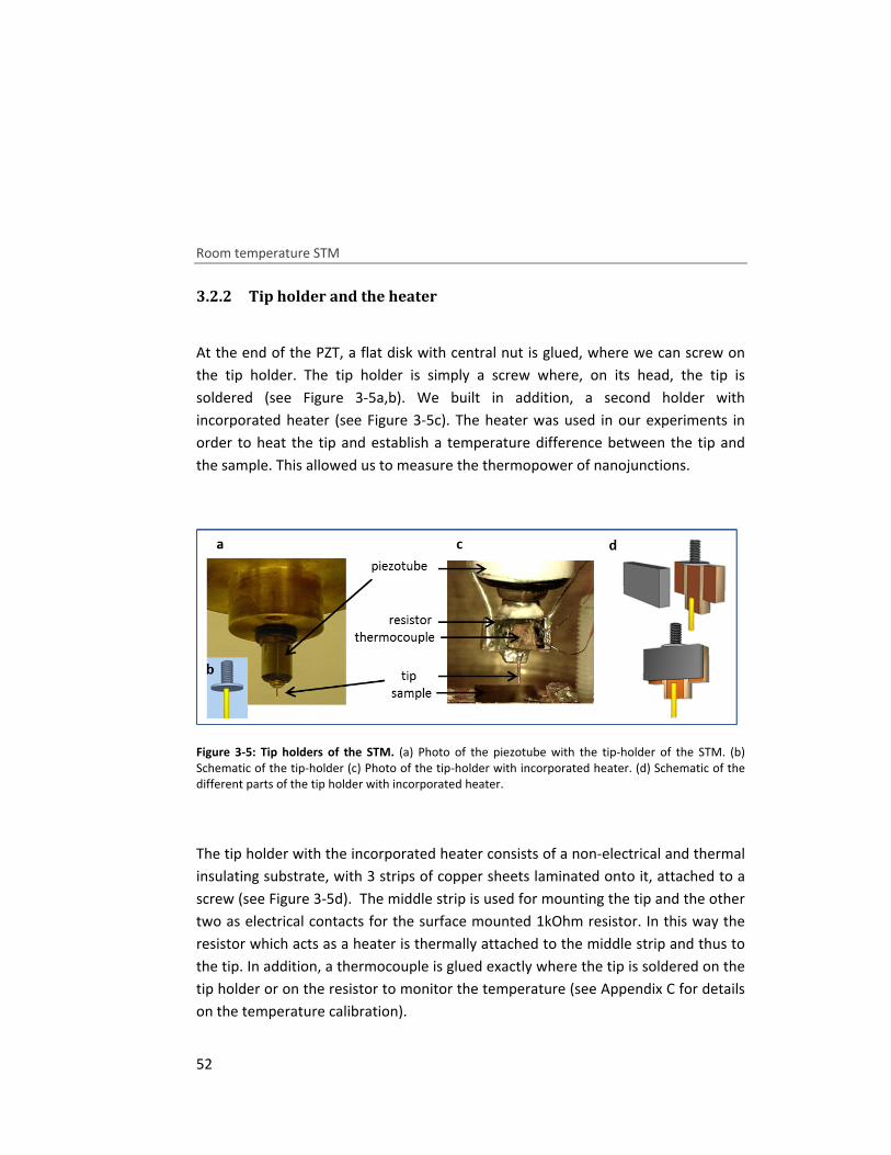
Room temperature STM
52
3.2.2 Tip holder and the heater
At the end of the PZT, a flat disk with central nut is glued, where we can screw on
the tip holder. The tip holder is simply a screw where, on its head, the tip is
soldered (see Figure 3-5a,b). We built in addition, a second holder with
incorporated heater (see Figure 3-5c). The heater was used in our experiments in
order to heat the tip and establish a temperature difference between the tip and
the sample. This allowed us to measure the thermopower of nanojunctions.
Figure 3-5: Tip holders of the STM. (a) Photo of the piezotube with the tip-holder of the STM. (b) Schematic of the tip-holder (c) Photo of the tip-holder with incorporated heater. (d) Schematic of the different parts of the tip holder with incorporated heater.
The tip holder with the incorporated heater consists of a non-electrical and thermal
insulating substrate, with 3 strips of copper sheets laminated onto it, attached to a
screw (see Figure 3-5d). The middle strip is used for mounting the tip and the other
two as electrical contacts for the surface mounted 1kOhm resistor. In this way the
resistor which acts as a heater is thermally attached to the middle strip and thus to
the tip. In addition, a thermocouple is glued exactly where the tip is soldered on the
tip holder or on the resistor to monitor the temperature (see Appendix C for details
on the temperature calibration).
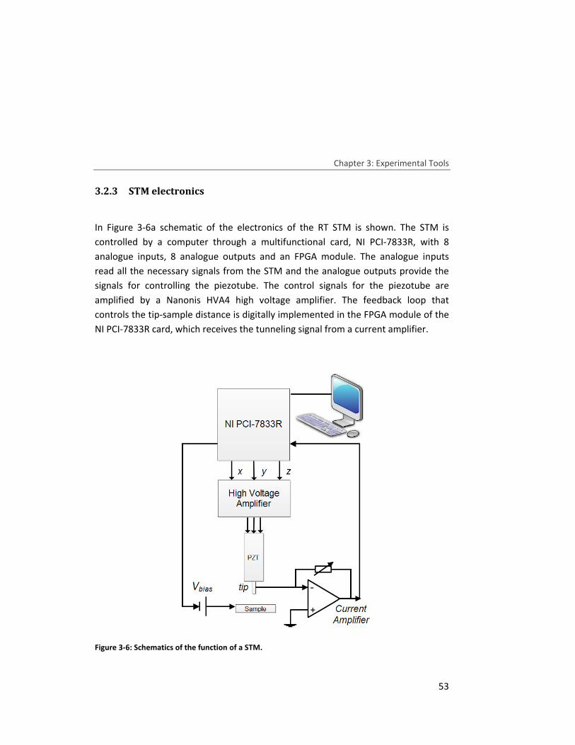
Chapter 3: Experimental Tools
53
3.2.3 STM electronics
In Figure 3-6a schematic of the electronics of the RT STM is shown. The STM is
controlled by a computer through a multifunctional card, NI PCI-7833R, with 8
analogue inputs, 8 analogue outputs and an FPGA module. The analogue inputs
read all the necessary signals from the STM and the analogue outputs provide the
signals for controlling the piezotube. The control signals for the piezotube are
amplified by a Nanonis HVA4 high voltage amplifier. The feedback loop that
controls the tip-sample distance is digitally implemented in the FPGA module of the
NI PCI-7833R card, which receives the tunneling signal from a current amplifier.
Figure 3-6: Schematics of the function of a STM.
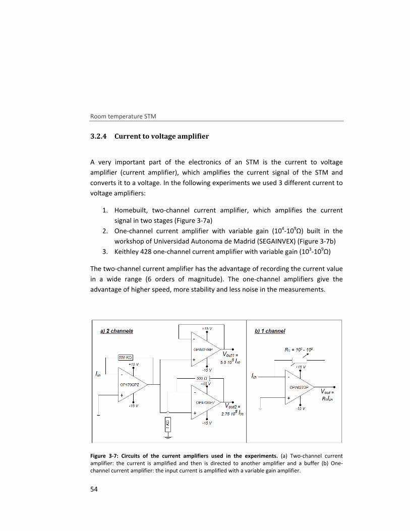
Room temperature STM
54
3.2.4 Current to voltage amplifier
A very important part of the electronics of an STM is the current to voltage
amplifier (current amplifier), which amplifies the current signal of the STM and
converts it to a voltage. In the following experiments we used 3 different current to
voltage amplifiers:
1. Homebuilt, two-channel current amplifier, which amplifies the current
signal in two stages (Figure 3-7a)
2. One-channel current amplifier with variable gain (104-109Ω) built in the
workshop of Universidad Autonoma de Madrid (SEGAINVEX) (Figure 3-7b)
3. Keithley 428 one-channel current amplifier with variable gain (103-109Ω)
The two-channel current amplifier has the advantage of recording the current value
in a wide range (6 orders of magnitude). The one-channel amplifiers give the
advantage of higher speed, more stability and less noise in the measurements.
Figure 3-7: Circuits of the current amplifiers used in the experiments. (a) Two-channel current amplifier: the current is amplified and then is directed to another amplifier and a buffer (b) One-channel current amplifier: the input current is amplified with a variable gain amplifier.
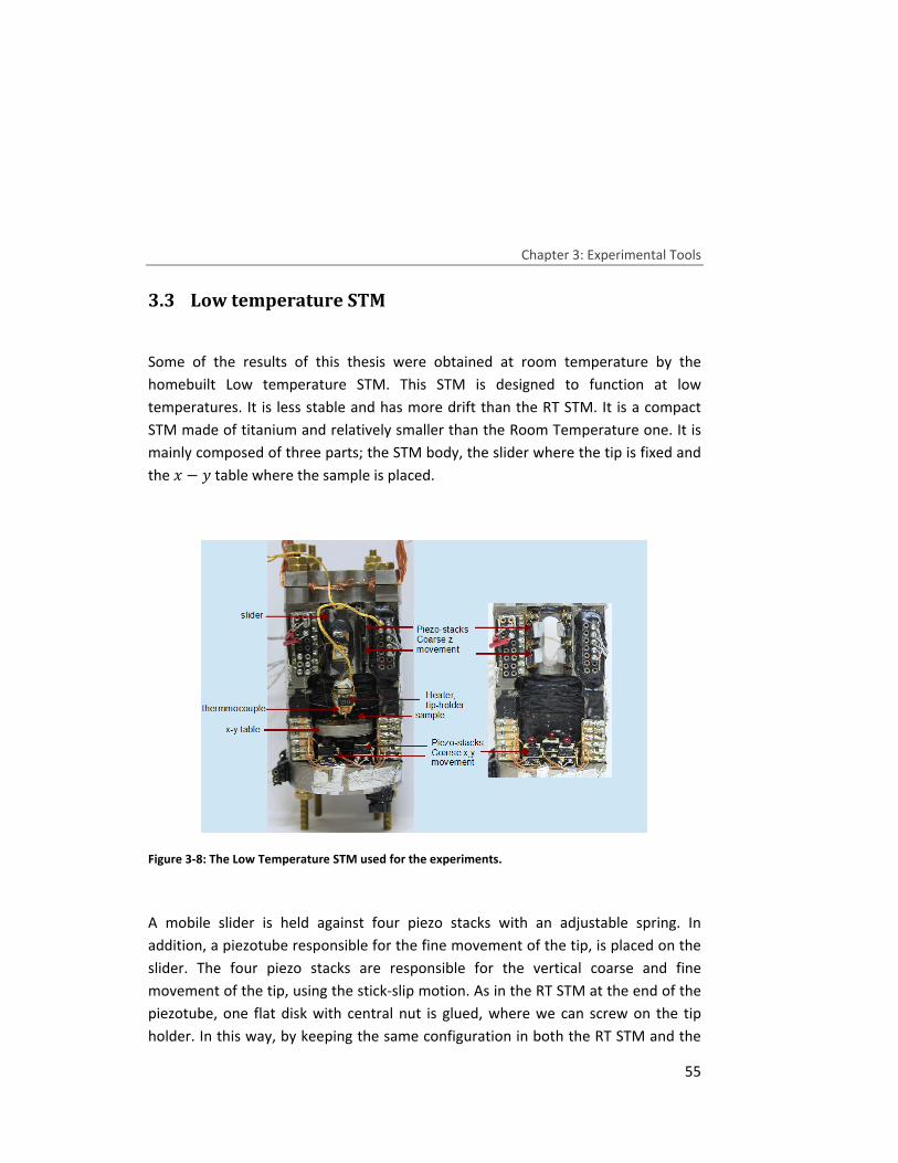
Chapter 3: Experimental Tools
55
3.3 Low temperature STM
Some of the results of this thesis were obtained at room temperature by the
homebuilt Low temperature STM. This STM is designed to function at low
temperatures. It is less stable and has more drift than the RT STM. It is a compact
STM made of titanium and relatively smaller than the Room Temperature one. It is
mainly composed of three parts; the STM body, the slider where the tip is fixed and
the 1 − ¾ table where the sample is placed.
Figure 3-8: The Low Temperature STM used for the experiments.
A mobile slider is held against four piezo stacks with an adjustable spring. In
addition, a piezotube responsible for the fine movement of the tip, is placed on the
slider. The four piezo stacks are responsible for the vertical coarse and fine
movement of the tip, using the stick-slip motion. As in the RT STM at the end of the
piezotube, one flat disk with central nut is glued, where we can screw on the tip
holder. In this way, by keeping the same configuration in both the RT STM and the
Low temperature STM
56
LT STM, we can adjust the same tip holders on both (one with incorporated heater
and one without).
The 1 − ¾ table is a mobile disk with an alumina lamina glued on its base and it’s
held against the piezo stacks with an adjustable spring. Each stack is composed of a
pair of piezostacks oriented in the 1 and ¾ direction, and they are responsible for
the coarse and fine movement in the x and y direction.
Each piezo stack is built up from four piezoelectric plates and copper sheets in
between them glued by silver epoxy. On top of each piezo stack, an alumina lamina
has been glued by epoxy (Stycast). Additionally, for the 1 − ¾ stacks, a small sphere
is glued on top of the alumina for a more stable contact with the 1¾ table. In our
experiments we used the piezo-stacks to control the 1 − ¾ − ¿ coarse movement
and the piezotube for the 1 − ¾ − ¿ fine movement.
A detailed description of the specific STM and the function of the piezo-stacks is
already presented in ref. [Arroyo2010]. We did not change the metallic parts but we
had rebuilt the piezo-electric elements.

Chapter 3: Experimental Tools
57
References
[Arroyo2010] Arroyo, C. (2010). Electron transport and phonons in atomic wires and
single molecule junctions. [Binnig1982] Binnig, G., H. Rohrer, C. Gerber and E. Weibel (1982). "Tunneling
through a controllable vacuum gap." Applied Physics Letters 40(2): 178-180. [Wiesendanger1994] Wiesendanger, R. (1994). Scanning Probe Microscopy and
Spectroscopy: Methods and Applications, Cambridge University Press.

The characterization of a junction at the molecular
monitoring of its conductance during formation and subsequent breaking
thesis we developed a novel technique for measuring therm
junctions which
simultaneous measurement of thermopower and conductance.
4.1
A complete characterization of a nanojunction (molecul
atomic
evolution of the junction. The most used
Break
technique for atomic metallic contacts
driv
substrate material is usually gold.
made, the tip is withdrawn, and the conductance is recorded
more m
when the metallic contact breaks,
junction
plateau
Chapter
The characterization of a junction at the molecular
monitoring of its conductance during formation and subsequent breaking
thesis we developed a novel technique for measuring therm
junctions which
simultaneous measurement of thermopower and conductance.
4.1 Introduction
A complete characterization of a nanojunction (molecul
atomic contacts) needs the conductance
evolution of the junction. The most used
Break-Junction technique demonstrated by N.J. Tao
technique for atomic metallic contacts
driven in and out of contact with a
substrate material is usually gold.
made, the tip is withdrawn, and the conductance is recorded
more molecules that are present
when the metallic contact breaks,
junction will be through the one or more molecules
lateau in the �
Chapter 4: Simultaneous Thermopower and Conductance Measurement Technique
The characterization of a junction at the molecular
monitoring of its conductance during formation and subsequent breaking
thesis we developed a novel technique for measuring therm
junctions which, in contrast to previously reported techniques
simultaneous measurement of thermopower and conductance.
Introduction
A complete characterization of a nanojunction (molecul
contacts) needs the conductance
evolution of the junction. The most used
Junction technique demonstrated by N.J. Tao
technique for atomic metallic contacts
and out of contact with a
substrate material is usually gold.
made, the tip is withdrawn, and the conductance is recorded
olecules that are present
when the metallic contact breaks,
be through the one or more molecules� − ¿ (¿ is the tip movement in the vertical direction)
Simultaneous Thermopower and Conductance Measurement Technique
The characterization of a junction at the molecular
monitoring of its conductance during formation and subsequent breaking
thesis we developed a novel technique for measuring therm
in contrast to previously reported techniques
simultaneous measurement of thermopower and conductance.
A complete characterization of a nanojunction (molecul
contacts) needs the conductance
evolution of the junction. The most used
Junction technique demonstrated by N.J. Tao
technique for atomic metallic contacts [Agraït1993
and out of contact with a substrate covered
substrate material is usually gold. Once the contact between tip and surface is
made, the tip is withdrawn, and the conductance is recorded
olecules that are present, may bind at
when the metallic contact breaks, the main charge transport pathway across the
be through the one or more molecules
is the tip movement in the vertical direction)
Simultaneous Thermopower and Conductance Measurement Technique
The characterization of a junction at the molecular
monitoring of its conductance during formation and subsequent breaking
thesis we developed a novel technique for measuring therm
in contrast to previously reported techniques
simultaneous measurement of thermopower and conductance.
A complete characterization of a nanojunction (molecul
contacts) needs the conductance (�) to be measured during the whole
evolution of the junction. The most used STM based
Junction technique demonstrated by N.J. Tao [Xu2003
Agraït1993]. In this technique the STM tip is
substrate covered
Once the contact between tip and surface is
made, the tip is withdrawn, and the conductance is recorded
may bind at both the tip and the sample
the main charge transport pathway across the
be through the one or more molecules.
is the tip movement in the vertical direction)
Simultaneous Thermopower and Conductance Measurement Technique
The characterization of a junction at the molecular or atomic
monitoring of its conductance during formation and subsequent breaking
thesis we developed a novel technique for measuring thermopower in nanoscale
in contrast to previously reported techniques
simultaneous measurement of thermopower and conductance.
A complete characterization of a nanojunction (molecular junction or metallic
to be measured during the whole
STM based technique up to now is STM
Xu2003] which
In this technique the STM tip is
substrate covered with molecules.
Once the contact between tip and surface is
made, the tip is withdrawn, and the conductance is recorded (Figure
both the tip and the sample
the main charge transport pathway across the
This results in a conductance
is the tip movement in the vertical direction)
Simultaneous Thermopower and Conductance Measurement Technique
or atomic level requires
monitoring of its conductance during formation and subsequent breaking. In this
opower in nanoscale
in contrast to previously reported techniques, allows for the
junction or metallic
to be measured during the whole
technique up to now is STM
which is based on the
In this technique the STM tip is
molecules. Tip and
Once the contact between tip and surface is
Figure 4-1a). One or
both the tip and the sample,
the main charge transport pathway across the
This results in a conductance
is the tip movement in the vertical direction) trace upon
Simultaneous Thermopower and Conductance Measurement Technique
59
level requires
. In this
opower in nanoscale
allows for the
junction or metallic
to be measured during the whole
technique up to now is STM
based on the
In this technique the STM tip is
Tip and
Once the contact between tip and surface is
One or
and
the main charge transport pathway across the
This results in a conductance
upon
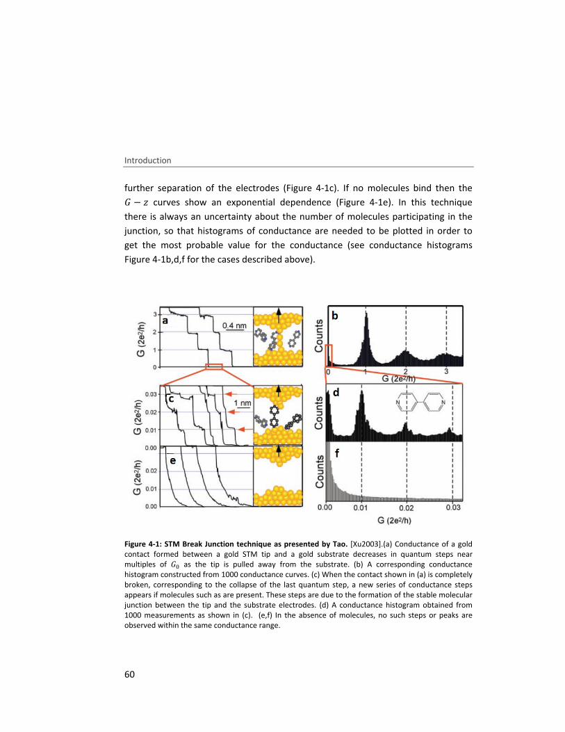
Introduction
60
further separation of the electrodes (Figure 4-1c). If no molecules bind then the � − ¿ curves show an exponential dependence (Figure 4-1e). In this technique
there is always an uncertainty about the number of molecules participating in the
junction, so that histograms of conductance are needed to be plotted in order to
get the most probable value for the conductance (see conductance histograms
Figure 4-1b,d,f for the cases described above).
Figure 4-1: STM Break Junction technique as presented by Tao. [Xu2003].(a) Conductance of a gold contact formed between a gold STM tip and a gold substrate decreases in quantum steps near multiples of � as the tip is pulled away from the substrate. (b) A corresponding conductance histogram constructed from 1000 conductance curves. (c) When the contact shown in (a) is completely broken, corresponding to the collapse of the last quantum step, a new series of conductance steps appears if molecules such as are present. These steps are due to the formation of the stable molecular junction between the tip and the substrate electrodes. (d) A conductance histogram obtained from 1000 measurements as shown in (c). (e,f) In the absence of molecules, no such steps or peaks are observed within the same conductance range.
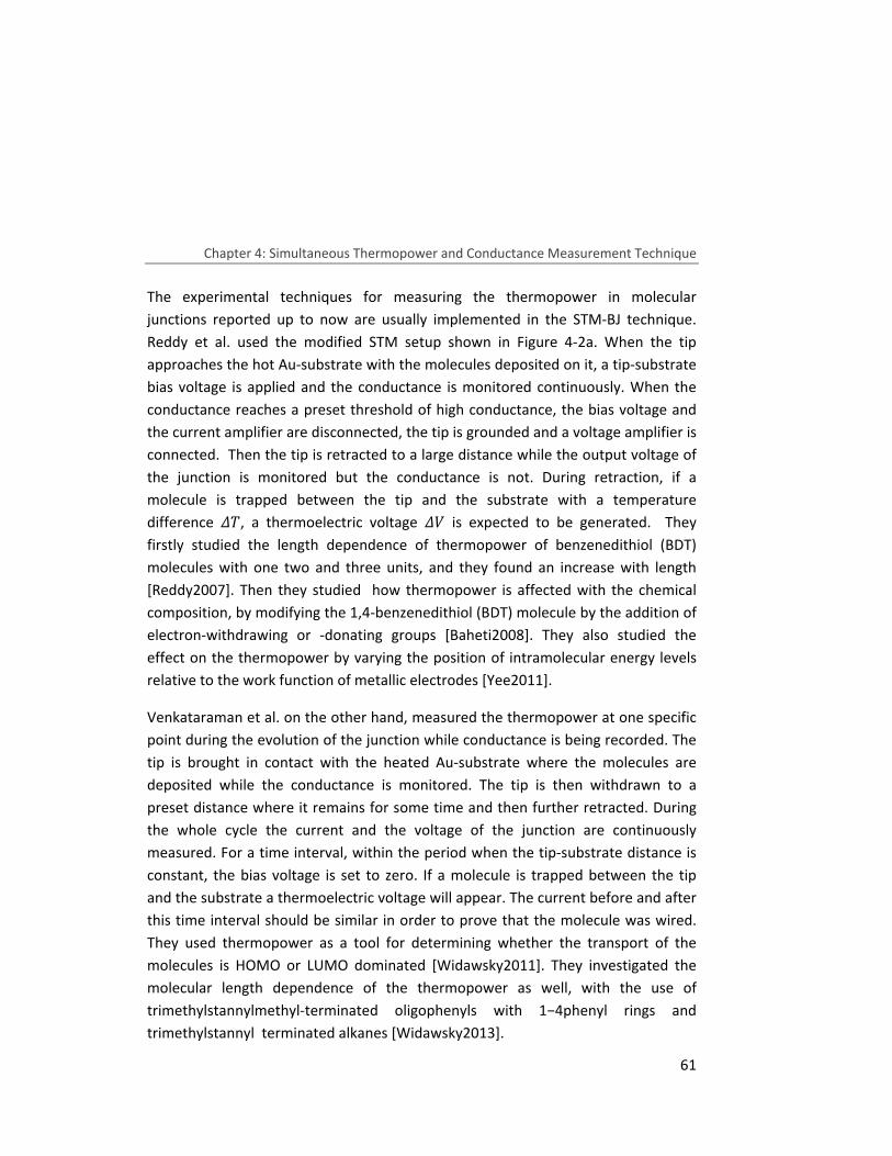
Chapter 4: Simultaneous Thermopower and Conductance Measurement Technique
61
The experimental techniques for measuring the thermopower in molecular
junctions reported up to now are usually implemented in the STM-BJ technique.
Reddy et al. used the modified STM setup shown in Figure 4-2a. When the tip
approaches the hot Au-substrate with the molecules deposited on it, a tip-substrate
bias voltage is applied and the conductance is monitored continuously. When the
conductance reaches a preset threshold of high conductance, the bias voltage and
the current amplifier are disconnected, the tip is grounded and a voltage amplifier is
connected. Then the tip is retracted to a large distance while the output voltage of
the junction is monitored but the conductance is not. During retraction, if a
molecule is trapped between the tip and the substrate with a temperature
difference ��, a thermoelectric voltage �� is expected to be generated. They
firstly studied the length dependence of thermopower of benzenedithiol (BDT)
molecules with one two and three units, and they found an increase with length
[Reddy2007]. Then they studied how thermopower is affected with the chemical
composition, by modifying the 1,4-benzenedithiol (BDT) molecule by the addition of
electron-withdrawing or -donating groups [Baheti2008]. They also studied the
effect on the thermopower by varying the position of intramolecular energy levels
relative to the work function of metallic electrodes [Yee2011].
Venkataraman et al. on the other hand, measured the thermopower at one specific
point during the evolution of the junction while conductance is being recorded. The
tip is brought in contact with the heated Au-substrate where the molecules are
deposited while the conductance is monitored. The tip is then withdrawn to a
preset distance where it remains for some time and then further retracted. During
the whole cycle the current and the voltage of the junction are continuously
measured. For a time interval, within the period when the tip-substrate distance is
constant, the bias voltage is set to zero. If a molecule is trapped between the tip
and the substrate a thermoelectric voltage will appear. The current before and after
this time interval should be similar in order to prove that the molecule was wired.
They used thermopower as a tool for determining whether the transport of the
molecules is HOMO or LUMO dominated [Widawsky2011]. They investigated the
molecular length dependence of the thermopower as well, with the use of
trimethylstannylmethyl-terminated oligophenyls with 1−4phenyl rings and
trimethylstannyl terminated alkanes [Widawsky2013].
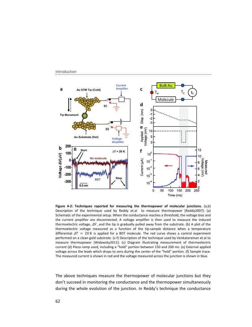
Introduction
62
Figure 4-2: Techniques reported for measuring the thermopower of molecular junctions. (a,b) Description of the technique used by Reddy et.al to measure thermopower [Reddy2007]: (a) Schematic of the experimental setup. When the conductance reaches a threshold, the voltage bias and the current amplifier are disconnected. A voltage amplifier is then used to measure the induced thermoelectric voltage, ��, and the tip is gradually pulled away from the substrate. (b) A plot of the thermoelectric voltage measured as a function of the tip-sample distance when a temperature differential �� = 20K is applied for a BDT molecule. The red curve shows a control experiment performed on a clean gold substrate. (c-f) Description of the technique used by Venkataraman et.al to measure thermopower [Widawsky2011]: (c) Diagram illustrating measurement of thermoelectric current (d) Piezo ramp used, including a “hold” portion between 150 and 200 ms. (e) External applied voltage across the leads which drops to zero during the center of the “hold” portion. (f) Sample trace. The measured current is shown in red and the voltage measured across the junction is shown in blue.
The above techniques measure the thermopower of molecular junctions but they
don’t succeed in monitoring the conductance and the thermopower simultaneously
during the whole evolution of the junction. In Reddy’s technique the conductance
Chapter 4: Simultaneous Thermopower and Conductance Measurement Technique
63
and the thermopower are not measured in the same junction, while in
Vencataraman’s technique they are, but the thermopower is measured just at one
point of the junction. In contrast to these previous experiments, we developed a
new technique that makes possible to measure thermopower and conductance
simultaneously during the whole evolution of the molecular junction. The technique
is described in the following section.
4.2 The technique
A temperature difference between the tip and the substrate is established by
heating the tip and keeping the substrate at room temperature (further information
about heating the tip can be found in Appendix C). The temperature stabilizes after
15 minutes while the minimization of the drift takes several hours. During an
approach-retraction cycle of the tip (see Figure 4-3a-c) the bias voltage is
maintained at a fixed value ���� and every few picometers the tip motion stops
(see Figure 4-3e) and the voltage is swept between Ä∆� (Figure 4-3f). In each
closing-opening cycle, several hundred current versus voltage curves, or − �
curves, are acquired. The corresponding − � curves, show a Temperature-
dependent thermal voltage �mn (see Figure 4-3g).
When a temperature difference�� is applied across the material, an electric
potential difference �� = −��� appears in response (Seebeck effect), where � is
the Seebeck coefficient. The thermovoltage �mn , consists of a contribution from
the junction �(�n − �Ç) and a contribution from the tip-connecting
lead� ��(�È − �ℎ), where � and �=v�a are the thermopower of the junction and
the lead, respectively.
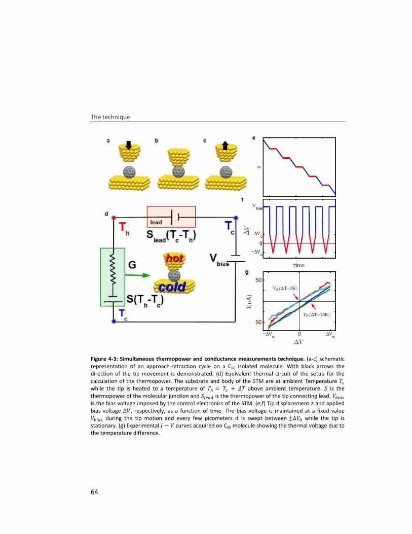
The technique
64
Figure 4-3: Simultaneous thermopower and conductance measurements technique. (a-c) schematic representation of an approach-retraction cycle on a C60 isolated molecule. With black arrows the direction of the tip movement is demonstrated. (d) Equivalent thermal circuit of the setup for the calculation of the thermopower. The substrate and body of the STM are at ambient Temperature �Ç while the tip is heated to a temperature of �n =�Ç + �� above ambient temperature. � is the thermopower of the molecular junction and �=v�a is the thermopower of the tip connecting lead. �Å��� is the bias voltage imposed by the control electronics of the STM. (e,f) Tip displacement ¿ and applied bias voltage ∆�, respectively, as a function of time. The bias voltage is maintained at a fixed value �Å��� during the tip motion and every few picometers it is swept betweenÄ∆� while the tip is stationary. (g) Experimental − � curves acquired on C60 molecule showing the thermal voltage due to the temperature difference.

Chapter 4: Simultaneous Thermopower and Conductance Measurement Technique
65
Considering the equivalent circuit (Figure 4-3d), we can write:
where �Å��� is the bias voltage,�Ç is the temperature of the sample and �n = �Ç +�� is the temperature of the tip.
Taking into account that when ���� = �mn the current vanishes, and from Equation
4-1 we can write
Thus by measuring an − � curve, we can obtain simultaneously the thermopower � and the conductance �: the zero crossing yields �mn (and thence we can obtain �)
and the slope gives �. Further information for the estimation of �=v�a value can be
found in Appendix D.
4.3 Thermopower circuit -voltage offsets
The magnitude the thermopower we want to measure is very small and
consequently a dynamical calibration of the electronics is required. Various
electronical offsets have a tendency to drift in time during the experiment. Here we
describe the offsets appearing and the calibration procedure.
• The bias voltage offset (��): the bias voltage is applied by a digital-to-analogue
converter (DAC), which has a small offset.
• The current amplifier input offset voltage (�v): voltage offset in the STM current
circuit due to the current amplifier whose virtual ground is not exactly at zero
volts.
� = �Å��� − �mn = �Å��� − �(�n − �Ç) − �=v�a(�Ç − �n)= �Å��� − ��� + �=v�a��, Equation 4-1
�mn = −��� + �=v�a�� = −(� − �=v�a)��. Equation 4-2
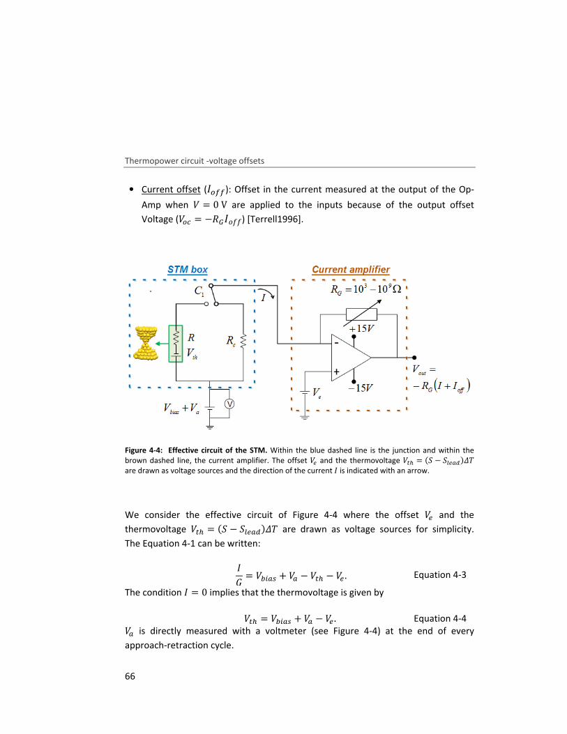
Thermopower circuit -voltage offsets
66
• Current offset (Éww): Offset in the current measured at the output of the Op-
Amp when � = 0V are applied to the inputs because of the output offset
Voltage (�ÉÇ = −�§W&&) [Terrell1996].
Figure 4-4: Effective circuit of the STM. Within the blue dashed line is the junction and within the brown dashed line, the current amplifier. The offset �v and the thermovoltage �mn = (� − �=v�a)�� are drawn as voltage sources and the direction of the current is indicated with an arrow.
We consider the effective circuit of Figure 4-4 where the offset �v and the
thermovoltage �mn = (� − �=v�a)�� are drawn as voltage sources for simplicity.
The Equation 4-1 can be written:
The condition = 0 implies that the thermovoltage is given by
�� is directly measured with a voltmeter (see Figure 4-4) at the end of every
approach-retraction cycle.
� = �Å��� + �� − �mn − �v . Equation 4-3
�mn = �Å��� + �� − �v . Equation 4-4
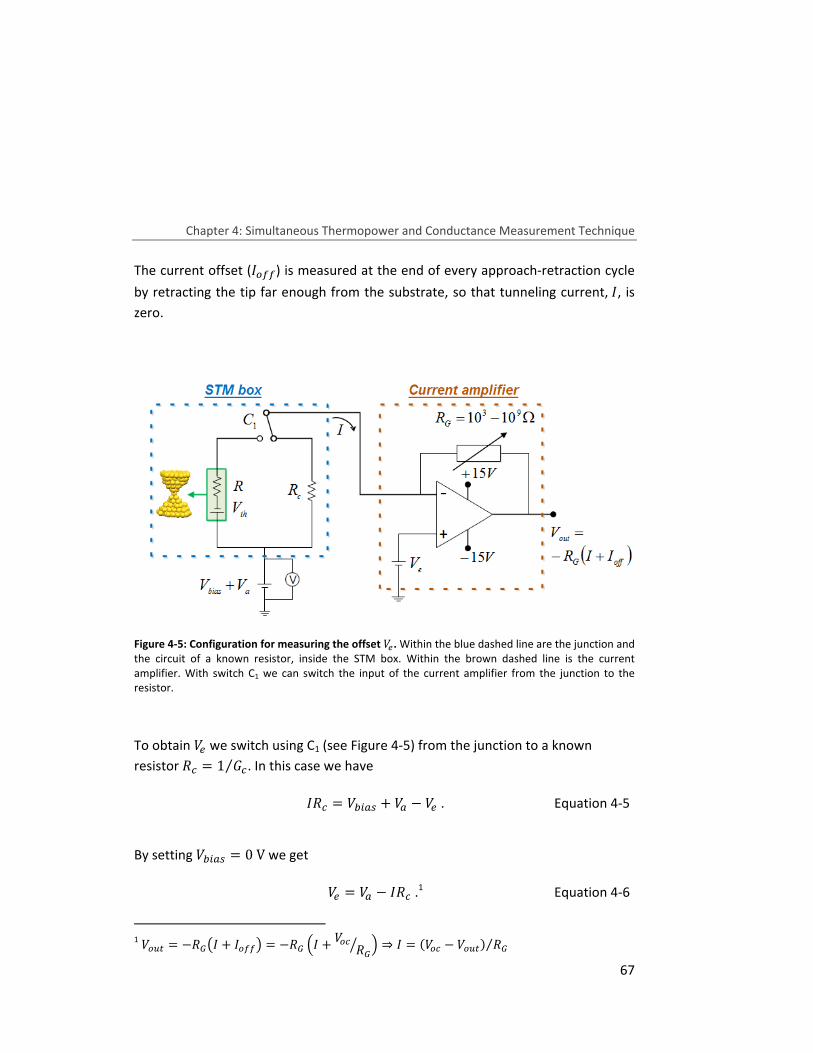
Chapter 4: Simultaneous Thermopower and Conductance Measurement Technique
67
The current offset (Éww) is measured at the end of every approach-retraction cycle
by retracting the tip far enough from the substrate, so that tunneling current,, is
zero.
Figure 4-5: Configuration for measuring the offset �v. Within the blue dashed line are the junction and the circuit of a known resistor, inside the STM box. Within the brown dashed line is the current amplifier. With switch C1 we can switch the input of the current amplifier from the junction to the resistor.
To obtain �v we switch using C1 (see Figure 4-5) from the junction to a known
resistor �Ç = 1 �Ç⁄ . In this case we have
By setting ���� = 0V we get
1 �É�m = −�§� + Éww� = −�§ K + �ÉÇ �§� L ⇒ = (�ÉÇ − �É�m) �§⁄
�Ç = �Å��� + �� − �v. Equation 4-5
�v = �� − �Ç.1 Equation 4-6
Thermopower circuit -voltage offsets
68
The resistor should be of similar value to the resistance of the junction being
measured and is installed inside the STM box in parallel to the STM-circuit. We
switch to the known resistor and measure the current amplifier input offset voltage, �v, at the end of every 50-100 approach-retraction cycles.
As shown above the electronical offsets are related to the operational amplifier
(Op-Amp) of the current to voltage amplifier. In order to minimize these offsets is
better using a one channel current amplifier which just uses one Op-Amp in
contrast to the two channel current amplifier which uses two Op-Amps. For further
information for the Op-Amps see Appendix E.
Chapter 4: Simultaneous Thermopower and Conductance Measurement Technique
69
References
[Agraït1993] Agraït, N., J. G. Rodrigo and S. Vieira (1993). "Conductance steps and
quantization in atomic-size contacts." Physical Review B 47(18): 12345-12348.
[Baheti2008] Baheti, K., J. A. Malen, P. Doak, P. Reddy, S.-Y. Jang, et al. (2008). "Probing the Chemistry of Molecular Heterojunctions Using Thermoelectricity." Nano Letters 8(2): 715-719.
[Reddy2007] Reddy, P., S.-Y. Jang, R. A. Segalman and A. Majumdar (2007). "Thermoelectricity in Molecular Junctions." Science 315(5818): 1568-1571.
[Terrell1996] Terrell, D. (1996). Op Amps: Design, Application, and Troubleshooting: Design, Application, and Troubleshooting, Elsevier Science.
[Widawsky2013] Widawsky, J. R., W. Chen, H. Vázquez, T. Kim, R. Breslow, et al. (2013). "Length-Dependent Thermopower of Highly Conducting Au–C Bonded Single Molecule Junctions." Nano Letters 13(6): 2889-2894.
[Widawsky2011] Widawsky, J. R., P. Darancet, J. B. Neaton and L. Venkataraman (2011). "Simultaneous Determination of Conductance and Thermopower of Single Molecule Junctions." Nano Letters 12(1): 354-358.
[Xu2003] Xu, B. and N. J. Tao (2003). "Measurement of Single-Molecule Resistance by Repeated Formation of Molecular Junctions." Science 301(5637): 1221-1223.
[Yee2011] Yee, S. K., J. A. Malen, A. Majumdar and R. A. Segalman (2011). "Thermoelectricity in Fullerene–Metal Heterojunctions." Nano Letters 11(10): 4089-4094.

71

In
junctions at room temperature in ambient conditions. C
for future electronic devices due to its physical properties
acceptor capability
Cu substrates
and ultrahigh
unexplored.
C60
the
of a molecular junction
5.1
Since the first
[Xu2003
by different factors
conductance with conjugation variations (
differennt ancoring groups used
[Arroyo2011
this chapter
junctions at room temperature in ambient conditions. C
for future electronic devices due to its physical properties
acceptor capability
Cu substrates, have been
and ultrahigh
unexplored. In the first section of this
junctions. The second
these junctions
of a molecular junction
5.1 Conductance characterization of
junctions
Since the first
Xu2003] the electronic transport trough
by different factors
conductance with conjugation variations (
differennt ancoring groups used
Arroyo2011; Cheng2011
Chapter 5: Engineering the Thermopower of Fullerene Molecular Junctions
we investigate
junctions at room temperature in ambient conditions. C
for future electronic devices due to its physical properties
acceptor capability [Guldi2000
have been widely studied with STM
vacuum; however
In the first section of this
The second section
junctions and demonstrates the possibility of engineering the thermo
of a molecular junction by nanoscale manipulations.
Conductance characterization of
junctions
Since the first reported conductance measurements of molecular junctions
the electronic transport trough
by different factors have been
conductance with conjugation variations (
differennt ancoring groups used
Cheng2011], with
Engineering the Thermopower of Fullerene Molecular Junctions
investigate the thermoelectrical properties of C
junctions at room temperature in ambient conditions. C
for future electronic devices due to its physical properties
Guldi2000; Langa2007
widely studied with STM
vacuum; however, its thermoelectric prope
In the first section of this chapter we
section focuse
and demonstrates the possibility of engineering the thermo
by nanoscale manipulations.
Conductance characterization of
conductance measurements of molecular junctions
the electronic transport trough
have been studied extensively
conductance with conjugation variations (
differennt ancoring groups used to bind the
with the length
Engineering the Thermopower of Fullerene Molecular Junctions
thermoelectrical properties of C
junctions at room temperature in ambient conditions. C
for future electronic devices due to its physical properties
Langa2007]. Electronic properties of C
widely studied with STM, especially in l
thermoelectric prope
chapter we characterize
focuses on the thermopower measurements of
and demonstrates the possibility of engineering the thermo
by nanoscale manipulations.
Conductance characterization of single
conductance measurements of molecular junctions
the electronic transport trough molecules and
extensively. For example
conductance with conjugation variations (eg. OPE-OPV)
to bind the metalic contacts
the length [Moreno
Engineering the Thermopower of Fullerene Molecular Junctions
thermoelectrical properties of C
junctions at room temperature in ambient conditions. C60 is a promising
for future electronic devices due to its physical properties - mainly
. Electronic properties of C
, especially in low te
thermoelectric properties
characterize single
the thermopower measurements of
and demonstrates the possibility of engineering the thermo
single- and double
conductance measurements of molecular junctions
and the way that
For example the dependence of
OPV) [Huber2007
metalic contacts (eg.
Moreno-García2013
Engineering the Thermopower of Fullerene Molecular Junctions
thermoelectrical properties of C60 molecular
promising candidate
mainly its electron
. Electronic properties of C60, mostly on
ow temperatures
rties remain largely
single- and double
the thermopower measurements of
and demonstrates the possibility of engineering the thermopower
and double-C60
conductance measurements of molecular junctions
the way that it is affected
the dependence of
Huber2007], with
(eg. Alkanes families)
García2013] and with
Engineering the Thermopower of Fullerene Molecular Junctions
73
molecular
candidate
electron-
mostly on
mperatures
remain largely
and double-
the thermopower measurements of
power
60
conductance measurements of molecular junctions
is affected
the dependence of
with the
s families)
with the
Conductance characterization of single- and double-C60 junctions
74
oxidation state [Chen2005]. In all these studies the STM Break-Junction technique
and the Mecanically Controlled Break Junction (MCBJ) technique have been used
[van Ruitenbeek1996]. However, using the break-junction techniques it remains
difficult to wire precisely one molecule, due to the lack of imaging possibilities and
the large number of molecules close to the junction. Thus, the conductance can
vary significantly from one junction to the next, and no obvious way exists to
differentiate one-molecule from multi-molecule related effects [Songmei2008;
Reuter2011; Reuter2012]. Statistics are required to obtain a most probable
conductance value from such measurements which may correspond to more than
one wired molecule [Arroyo2011] [French2012].
C60 is a relatively large molecule and that makes it possible to image it with STM
when deposited on metallic surface. Single pristine C60 molecules contacted
between metallic contacts have been fairly extensively studied on gold
[Joachim1995] and copper substrates [Néel2007; Néel2008; Schulze2008;
Arnau2011]. C60 dimers where formed in situ as well [Schull2009; Hauptmann2012].
All the above studies on C60 junctions have been done under UHV-STM conditions.
We have found that it is possible by using the image capability of the STM to target
individual isolated molecules and form stable single- and double-molecular
junctions in ambient conditions.
5.1.1 Single-C60 molecular junctions
We deposit the C60 molecules on flamed annealed gold surfaces by drop casting
using 1,2,4-trichlorobenzene (TCB) solution of concentration circa 10�Ì −10�¢Mand then we let it dry for several hours (further information about
deposition can be found in Appendix F). The STM images show small clusters and
isolated molecules immobilized at monoatomic steps or sometimes on the gold
terraces, as shown in Figure 5-1a. In order to focus on a particular single isolated
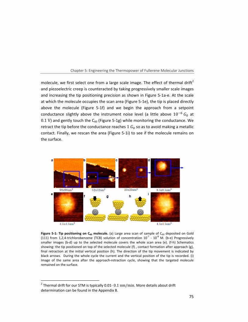
Chapter 5: Engineering the Thermopower of Fullerene Molecular Junctions
75
molecule, we first select one from a large scale image. The effect of thermal drift2
and piezoelectric creep is counteracted by taking progressively smaller scale images
and increasing the tip positioning precision as shown in Figure 5-1a-e. At the scale
at which the molecule occupies the scan area (Figure 5-1e), the tip is placed directly
above the molecule (Figure 5-1f) and we begin the approach from a setpoint
conductance slightly above the instrument noise level (a little above 10�� at 0.1V) and gently touch the C60 (Figure 5-1g) while monitoring the conductance. We
retract the tip before the conductance reaches 1� so as to avoid making a metallic
contact. Finally, we rescan the area (Figure 5-1i) to see if the molecule remains on
the surface.
Figure 5-1: Tip positioning on C60 molecule. (a) Large area scan of sample of C60 deposited on Gold (111) from 1,2,4-trichlorobenzene (TCB) solution of concentration 10-7 - 10-8 M. (b-e) Progressively smaller images (b-d) up to the selected molecule covers the whole scan area (e). (f-h) Schematics showing: the tip positioned on top of the selected molecule (f) , contact formation after approach (g), final retraction at the initial vertical position (h). The direction of the tip movement is indicated by black arrows. During the whole cycle the current and the vertical position of the tip is recorded. (i) Image of the same area after the approach-retraction cycle, showing that the targeted molecule remained on the surface.
2 Thermal drift for our STM is typically 0.01- 0.1nm/min. More details about drift determination can be found in the Appendix B.
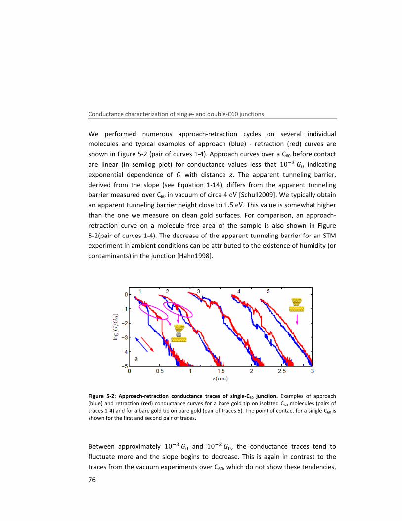
Conductance characterization of single- and double-C60 junctions
76
We performed numerous approach-retraction cycles on several individual
molecules and typical examples of approach (blue) - retraction (red) curves are
shown in Figure 5-2 (pair of curves 1-4). Approach curves over a C60 before contact
are linear (in semilog plot) for conductance values less that 10�N� indicating
exponential dependence of � with distance ¿. The apparent tunneling barrier,
derived from the slope (see Equation 1-14), differs from the apparent tunneling
barrier measured over C60 in vacuum of circa 4eV [Schull2009]. We typically obtain
an apparent tunneling barrier height close to 1.5eV. This value is somewhat higher
than the one we measure on clean gold surfaces. For comparison, an approach-
retraction curve on a molecule free area of the sample is also shown in Figure
5-2(pair of curves 1-4). The decrease of the apparent tunneling barrier for an STM
experiment in ambient conditions can be attributed to the existence of humidity (or
contaminants) in the junction [Hahn1998].
Figure 5-2: Approach-retraction conductance traces of single-C60 junction. Examples of approach (blue) and retraction (red) conductance curves for a bare gold tip on isolated C60 molecules (pairs of traces 1-4) and for a bare gold tip on bare gold (pair of traces 5). The point of contact for a single-C60 is shown for the first and second pair of traces.
Between approximately 10�N� and 10��� , the conductance traces tend to
fluctuate more and the slope begins to decrease. This is again in contrast to the
traces from the vacuum experiments over C60, which do not show these tendencies,
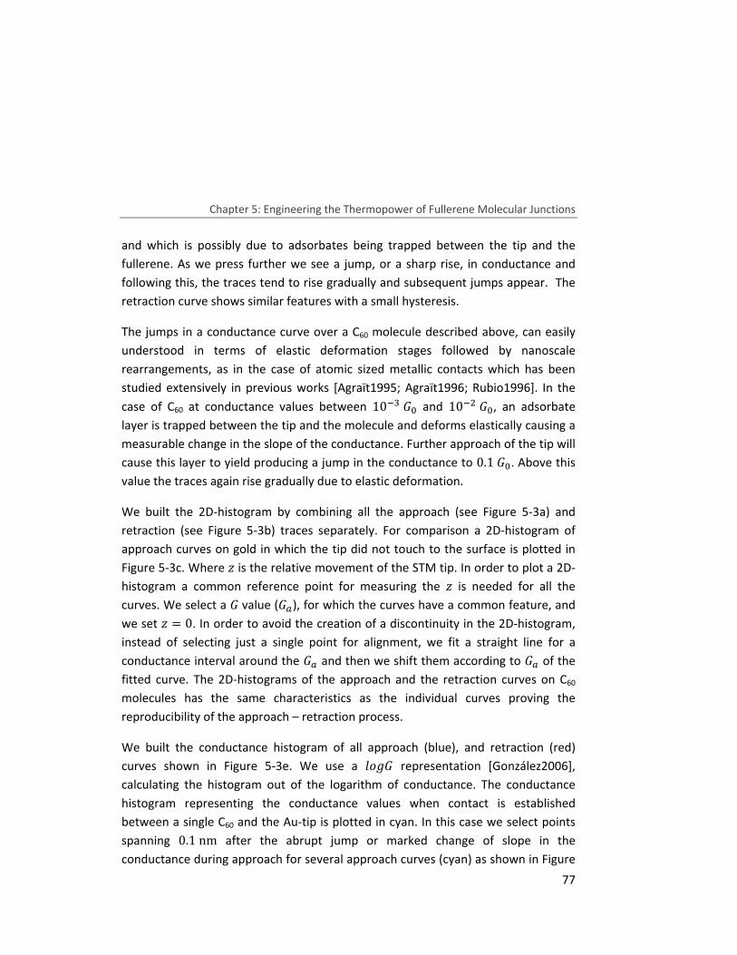
Chapter 5: Engineering the Thermopower of Fullerene Molecular Junctions
77
and which is possibly due to adsorbates being trapped between the tip and the
fullerene. As we press further we see a jump, or a sharp rise, in conductance and
following this, the traces tend to rise gradually and subsequent jumps appear. The
retraction curve shows similar features with a small hysteresis.
The jumps in a conductance curve over a C60 molecule described above, can easily
understood in terms of elastic deformation stages followed by nanoscale
rearrangements, as in the case of atomic sized metallic contacts which has been
studied extensively in previous works [Agraït1995; Agraït1996; Rubio1996]. In the
case of C60 at conductance values between 10�N� and 10��� , an adsorbate
layer is trapped between the tip and the molecule and deforms elastically causing a
measurable change in the slope of the conductance. Further approach of the tip will
cause this layer to yield producing a jump in the conductance to 0.1� . Above this
value the traces again rise gradually due to elastic deformation.
We built the 2D-histogram by combining all the approach (see Figure 5-3a) and
retraction (see Figure 5-3b) traces separately. For comparison a 2D-histogram of
approach curves on gold in which the tip did not touch to the surface is plotted in
Figure 5-3c. Where ¿ is the relative movement of the STM tip. In order to plot a 2D-
histogram a common reference point for measuring the ¿ is needed for all the
curves. We select a �value (��), for which the curves have a common feature, and
we set ¿ = 0. In order to avoid the creation of a discontinuity in the 2D-histogram,
instead of selecting just a single point for alignment, we fit a straight line for a
conductance interval around the �� and then we shift them according to �� of the
fitted curve. The 2D-histograms of the approach and the retraction curves on C60
molecules has the same characteristics as the individual curves proving the
reproducibility of the approach – retraction process.
We built the conductance histogram of all approach (blue), and retraction (red)
curves shown in Figure 5-3e. We use a Wz� representation [González2006],
calculating the histogram out of the logarithm of conductance. The conductance
histogram representing the conductance values when contact is established
between a single C60 and the Au-tip is plotted in cyan. In this case we select points
spanning 0.1nm after the abrupt jump or marked change of slope in the
conductance during approach for several approach curves (cyan) as shown in Figure
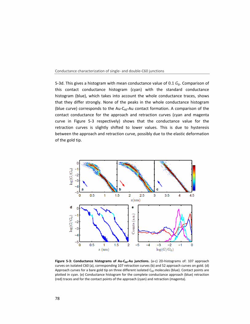
Conductance characterization of single- and double-C60 junctions
78
5-3d. This gives a histogram with mean conductance value of 0.1� . Comparison of
this contact conductance histogram (cyan) with the standard conductance
histogram (blue), which takes into account the whole conductance traces, shows
that they differ strongly. None of the peaks in the whole conductance histogram
(blue curve) corresponds to the Au-C60-Au contact formation. A comparison of the
contact conductance for the approach and retraction curves (cyan and magenta
curve in Figure 5-3 respectively) shows that the conductance value for the
retraction curves is slightly shifted to lower values. This is due to hysteresis
between the approach and retraction curve, possibly due to the elastic deformation
of the gold tip.
Figure 5-3: Conductance histograms of Au-C60-Au junctions. (a-c) 2D-histograms of: 107 approach curves on isolated C60 (a), corresponding 107 retraction curves (b) and 52 approach curves on gold. (d) Approach curves for a bare gold tip on three different isolated C60 molecules (blue). Contact points are plotted in cyan. (e) Conductance histogram for the complete conductance approach (blue) retraction (red) traces and for the contact points of the approach (cyan) and retraction (magenta).
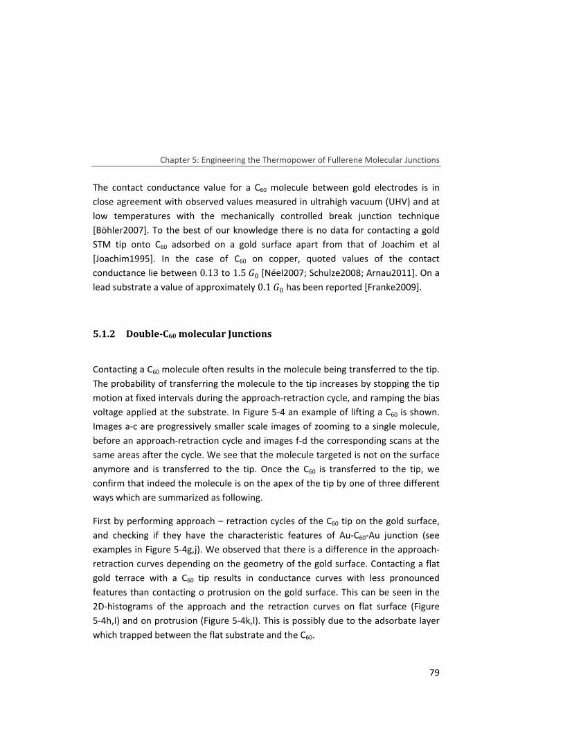
Chapter 5: Engineering the Thermopower of Fullerene Molecular Junctions
79
The contact conductance value for a C60 molecule between gold electrodes is in
close agreement with observed values measured in ultrahigh vacuum (UHV) and at
low temperatures with the mechanically controlled break junction technique
[Böhler2007]. To the best of our knowledge there is no data for contacting a gold
STM tip onto C60 adsorbed on a gold surface apart from that of Joachim et al
[Joachim1995]. In the case of C60 on copper, quoted values of the contact
conductance lie between 0.13 to 1.5� [Néel2007; Schulze2008; Arnau2011]. On a
lead substrate a value of approximately 0.1� has been reported [Franke2009].
5.1.2 Double-C60 molecular Junctions
Contacting a C60 molecule often results in the molecule being transferred to the tip.
The probability of transferring the molecule to the tip increases by stopping the tip
motion at fixed intervals during the approach-retraction cycle, and ramping the bias
voltage applied at the substrate. In Figure 5-4 an example of lifting a C60 is shown.
Images a-c are progressively smaller scale images of zooming to a single molecule,
before an approach-retraction cycle and images f-d the corresponding scans at the
same areas after the cycle. We see that the molecule targeted is not on the surface
anymore and is transferred to the tip. Once the C60 is transferred to the tip, we
confirm that indeed the molecule is on the apex of the tip by one of three different
ways which are summarized as following.
First by performing approach – retraction cycles of the C60 tip on the gold surface,
and checking if they have the characteristic features of Au-C60-Au junction (see
examples in Figure 5-4g,j). We observed that there is a difference in the approach-
retraction curves depending on the geometry of the gold surface. Contacting a flat
gold terrace with a C60 tip results in conductance curves with less pronounced
features than contacting o protrusion on the gold surface. This can be seen in the
2D-histograms of the approach and the retraction curves on flat surface (Figure
5-4h,I) and on protrusion (Figure 5-4k,l). This is possibly due to the adsorbate layer
which trapped between the flat substrate and the C60.
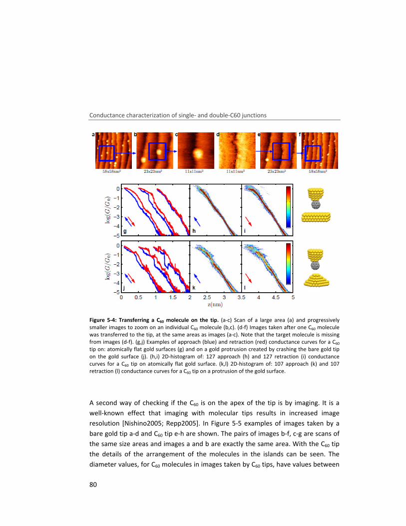
Conductance characterization of single- and double-C60 junctions
80
Figure 5-4: Transferring a C60 molecule on the tip. (a-c) Scan of a large area (a) and progressively smaller images to zoom on an individual C60 molecule (b,c). (d-f) Images taken after one C60 molecule was transferred to the tip, at the same areas as images (a-c). Note that the target molecule is missing from images (d-f). (g,j) Examples of approach (blue) and retraction (red) conductance curves for a C60 tip on: atomically flat gold surfaces (g) and on a gold protrusion created by crashing the bare gold tip on the gold surface (j). (h,i) 2D-histogram of: 127 approach (h) and 127 retraction (i) conductance curves for a C60 tip on atomically flat gold surface. (k,l) 2D-histogram of: 107 approach (k) and 107 retraction (l) conductance curves for a C60 tip on a protrusion of the gold surface.
A second way of checking if the C60 is on the apex of the tip is by imaging. It is a
well-known effect that imaging with molecular tips results in increased image
resolution [Nishino2005; Repp2005]. In Figure 5-5 examples of images taken by a
bare gold tip a-d and C60 tip e-h are shown. The pairs of images b-f, c-g are scans of
the same size areas and images a and b are exactly the same area. With the C60 tip
the details of the arrangement of the molecules in the islands can be seen. The
diameter values, for C60 molecules in images taken by C60 tips, have values between
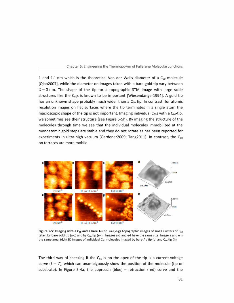
Chapter 5: Engineering the Thermopower of Fullerene Molecular Junctions
81
1 and 1.1nm which is the theoretical Van der Walls diameter of a C60 molecule
[Qiao2007], while the diameter on images taken with a bare gold tip vary between
2 − 3nm. The shape of the tip for a topographic STM image with large scale
structures like the C60s is known to be important [Wiesendanger1994]. A gold tip
has an unknown shape probably much wider than a C60 tip. In contrast, for atomic
resolution images on flat surfaces where the tip terminates in a single atom the
macroscopic shape of the tip is not important. Imaging individual C60s with a C60-tip,
we sometimes see their structure (see Figure 5-5h). By imaging the structure of the
molecules through time we see that the individual molecules immobilized at the
monoatomic gold steps are stable and they do not rotate as has been reported for
experiments in ultra-high vacuum [Gardener2009; Tang2011]. In contrast, the C60
on terraces are more mobile.
Figure 5-5: Imaging with a C60 and a bare Au tip. (a-c,e-g) Topographic images of small clusters of C60 taken by bare gold tip (a-c) and by C60 tip (e-h). Images a-b and e-f have the same size. Image a and e is the same area. (d,h) 3D images of individual C60 molecules imaged by bare-Au tip (d) and C60 tip (h).
The third way of checking if the C60 is on the apex of the tip is a current-voltage
curve ( − �), which can unambiguously show the position of the molecule (tip or
substrate). In Figure 5-4a, the approach (blue) – retraction (red) curve and the
Conductance characterization of single- and double-C60 junctions
82
points (circles) where each − � curve was recorded is shown. In Figure 5-4b
examples of − � curves recorded before (black) and after (magenta) the C60
molecule was transferred to the tip are plotted.
Figure 5-6: − � curves on top of a C60 molecule with Au tip and on top of Au with a C60 tip. (a,b) Approach (blue) - retraction (red) trace of Au tip on a C60. During this cycle the molecule is transferred to the tip (a). Circles with different colors on the retraction curve correspond to the points where we stop and the corresponding − � curves were taken (b). The current of the − � curves is normalized to the absolute highest current value of each curve. A strong increase of the current at positive bias voltage indicates that the C60 is on the surface, while an increase at negative bias voltage indicates that the C60 is on the tip. (c) Numerical derivative of a fitted cubic polynomial curve to the − � curves which reflects the electronic density of states as drawn on (d) and (e). Black corresponds to the black and grey bold line of the molecular levels at (d) and magenta to the magenta and dark magenta bold line at (e).
With an − � curve we can determine the electronic states of the sample
(occupied or unoccupied) contributing to the tunneling current
[Wiesendanger1994]. The − � curves on top of a C60 show that the Fermi energy is
closed to LUMO, because they are asymmetric with the tunneling current increasing
for positive ���� meaning that electrons tunnel from the occupied states of the Au-
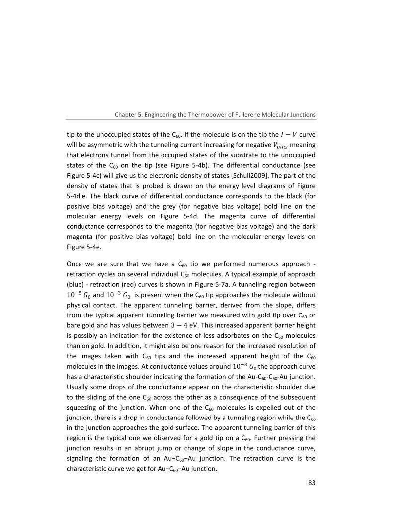
Chapter 5: Engineering the Thermopower of Fullerene Molecular Junctions
83
tip to the unoccupied states of the C60. If the molecule is on the tip the − � curve
will be asymmetric with the tunneling current increasing for negative ���� meaning
that electrons tunnel from the occupied states of the substrate to the unoccupied
states of the C60 on the tip (see Figure 5-4b). The differential conductance (see
Figure 5-4c) will give us the electronic density of states [Schull2009]. The part of the
density of states that is probed is drawn on the energy level diagrams of Figure
5-4d,e. The black curve of differential conductance corresponds to the black (for
positive bias voltage) and the grey (for negative bias voltage) bold line on the
molecular energy levels on Figure 5-4d. The magenta curve of differential
conductance corresponds to the magenta (for negative bias voltage) and the dark
magenta (for positive bias voltage) bold line on the molecular energy levels on
Figure 5-4e.
Once we are sure that we have a C60 tip we performed numerous approach -
retraction cycles on several individual C60 molecules. A typical example of approach
(blue) - retraction (red) curves is shown in Figure 5-7a. A tunneling region between 10�Ò� and 10�N� is present when the C60 tip approaches the molecule without
physical contact. The apparent tunneling barrier, derived from the slope, differs
from the typical apparent tunneling barrier we measured with gold tip over C60 or
bare gold and has values between 3 − 4eV. This increased apparent barrier height
is possibly an indication for the existence of less adsorbates on the C60 molecules
than on gold. In addition, it might also be one reason for the increased resolution of
the images taken with C60 tips and the increased apparent height of the C60
molecules in the images. At conductance values around 10�N� the approach curve
has a characteristic shoulder indicating the formation of the Au-C60-C60-Au junction.
Usually some drops of the conductance appear on the characteristic shoulder due
to the sliding of the one C60 across the other as a consequence of the subsequent
squeezing of the junction. When one of the C60 molecules is expelled out of the
junction, there is a drop in conductance followed by a tunneling region while the C60
in the junction approaches the gold surface. The apparent tunneling barrier of this
region is the typical one we observed for a gold tip on a C60. Further pressing the
junction results in an abrupt jump or change of slope in the conductance curve,
signaling the formation of an Au−C60−Au junction. The retraction curve is the
characteristic curve we get for Au−C60−Au junction.
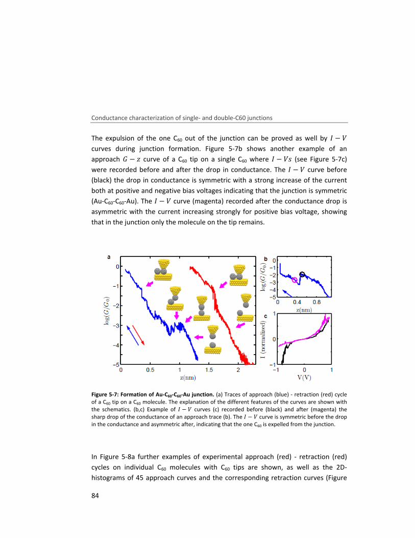
Conductance characterization of single- and double-C60 junctions
84
The expulsion of the one C60 out of the junction can be proved as well by − �
curves during junction formation. Figure 5-7b shows another example of an
approach � − ¿ curve of a C60 tip on a single C60 where − �Y (see Figure 5-7c)
were recorded before and after the drop in conductance. The − � curve before
(black) the drop in conductance is symmetric with a strong increase of the current
both at positive and negative bias voltages indicating that the junction is symmetric
(Au-C60-C60-Au). The − � curve (magenta) recorded after the conductance drop is
asymmetric with the current increasing strongly for positive bias voltage, showing
that in the junction only the molecule on the tip remains.
Figure 5-7: Formation of Au-C60-C60-Au junction. (a) Traces of approach (blue) - retraction (red) cycle of a C60 tip on a C60 molecule. The explanation of the different features of the curves are shown with the schematics. (b,c) Example of − � curves (c) recorded before (black) and after (magenta) the sharp drop of the conductance of an approach trace (b). The − � curve is symmetric before the drop in the conductance and asymmetric after, indicating that the one C60 is expelled from the junction.
In Figure 5-8a further examples of experimental approach (red) - retraction (red)
cycles on individual C60 molecules with C60 tips are shown, as well as the 2D-
histograms of 45 approach curves and the corresponding retraction curves (Figure
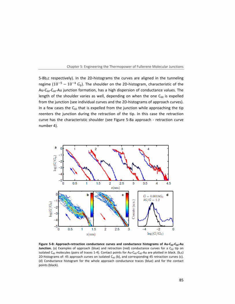
Chapter 5: Engineering the Thermopower of Fullerene Molecular Junctions
85
5-8b,c respectively). In the 2D-histograms the curves are aligned in the tunneling
regime (10�Ò − 10�Ó� ). The shoulder on the 2D-histogram, characteristic of the
Au-C60-C60-Au junction formation, has a high dispersion of conductance values. The
length of the shoulder varies as well, depending on when the one C60 is expelled
from the junction (see individual curves and the 2D-histograms of approach curves).
In a few cases the C60 that is expelled from the junction while approaching the tip
reenters the junction during the retraction of the tip. In this case the retraction
curve has the characteristic shoulder (see Figure 5-8a approach - retraction curve
number 4).
Figure 5-8: Approach-retraction conductance curves and conductance histograms of Au-C60-C60-Au
Junction. (a) Examples of approach (blue) and retraction (red) conductance curves for a C60 tip on isolated C60 molecules (pairs of traces 1-4). Contact points for Au-C60-C60-Au are plotted in black. (b,c) 2D-histograms of: 45 approach curves on isolated C60 (b), and corresponding 45 retraction curves (c). (d) Conductance histogram for the whole approach conductance traces (blue) and for the contact points (black).

Conductance characterization of single- and double-C60 junctions
86
From the 2D-histogram of retraction curves we see that the appearance of the
typical retraction curve of one C60 (see the high density red region of the histogram)
is more frequent.
We selected the data points from the shoulder of the approach curves up to the
point where the conductance starts increasing again as illustrated by the black part
of the approach curves in Figure 5-8a and out of these values we plotted the
conductance histogram in Figure 5-8d (black curve). For comparison, in the same
figure we plotted the standard conductance histogram by taking in to account the
whole conductance approach traces (blue curve). The peaks of both histograms
coincide, while for the Au-C60-Au junction, as mentioned in the previous section, the
peaks differ a lot (Figure 5-3e). The average conductance of this C60 dimer is
approximately 10�N� . The conductance of C60 dimers has been previously
reported using Cu electrodes, and as in the case of a single C60 between Cu
electrodes, higher values were found (~10��� ) [Schull2009].
We repeated the same approach-retraction cycles with C60 tips, on individual C60
molecules in organized and disorganized clusters. 2D-histograms of approach curves
with C60 tips on single C60s that are isolated, in clusters and in organized clusters are
shown in Figure 5-9a,b,c respectively. From the 2D-histograms it can be seen that
the conductance of the characteristic shoulder of the Au-C60-C60-Au junction
increases for clusters and even more for organized clusters. Molecules in a cluster
are less mobile than the isolated ones, thus the Au-C60-C60-Au junction formed is
more stable and the coupling between the two C60s is better, thus the conductance
reaches higher values. Furthermore, in an organized island, molecules are very
stable and a bigger force is needed to expel them from the junction. In addition, the
target molecule on the surface in a cluster is attached to other C60s and new paths
for electronic transport through the neighbouring molecules appear. As an analogy
we can think of a circuit with parallel resistors. The conductance value for a C60
dimer on an organized island is close to the values reported on Cu by Shull et al.
[Schull2009]. Finally, it is worth mentioning here that for a single-C60 junction of
molecules in clusters, we did not observe any difference in the conductance.
Chapter 5: Engineering the Thermopower of Fullerene Molecular Junctions
87
Figure 5-9: Double C60 junctions of isolated C60 and C60s in clusters. (a-c) 2D-histograms of: 45 approach curves of C60 tips on isolated C60s (a), 24 approach curves of C60 tips on C60s in clusters (b), 28 approach curves of C60 tips on C60s in organized clusters (c). (d-f) Characteristic images taken with C60 tip of: individual C60 (d), cluster of C60 (e), organized cluster of C60 (f).
5.2 Conductance of double-C60 junctions using DFT theory
To analyze the underlying transport mechanisms and to understand better the
dimer junction formation and the dispersion of the conductance values, we
performed large-scale quantum transport calculations on double-C60 junctions,
based on density functional theory (DFT) [Rocha2006], using the ab-initio code
SMEAGOL [Alexandre2005] which combines the Hamiltonian provided by the DFT
code SIESTA [Soler2002] with the non-equilibrium Green’s function formalism.
Further details about the above computation methods are given in Appendix K.
These calculations were performed together with K. Gillemot during my
secondment at the group of Prof. C.J. Lambert at Lancaster University.
First, we examined the geometry shown in Figure 5-10a. The electrodes were
assigned flat gold <111> surfaces to realistically model the large surface areas of
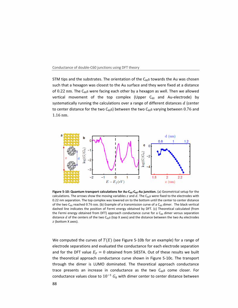
Conductance of double-C60 junctions using DFT theory
88
STM tips and the substrates. The orientation of the C60s towards the Au was chosen
such that a hexagon was closest to the Au surface and they were fixed at a distance
of 0.22nm. The C60s were facing each other by a hexagon as well. Then we allowed
vertical movement of the top complex (Upper C60 and Au-electrode) by
systematically running the calculations over a range of different distances � (center
to center distance for the two C60s) between the two C60s varying between 0.76 and 1.16nm.
Figure 5-10: Quantum transport calculations for Au-C60-C60-Au junction. (a) Geometrical setup for the calculations. The arrows show the moving variables ¿ and �. The C60s were fixed to the electrodes with 0.22 nm separation. The top complex was lowered on to the bottom until the center to center distance of the two C60 reached 0.76nm. (b) Example of a transmission curve of a C60 dimer. The black vertical dashed line indicates the position of Fermi energy obtained by DFT. (c) Theoretical calculated (from the Fermi energy obtained from DFT) approach conductance curve for a C60 dimer versus separation distance � of the centers of the two C60s (top X axes) and the distance between the two Au electrodes ¿ (bottom X axes).
We computed the curves of �(+) (see Figure 5-10b for an example) for a range of
electrode separations and evaluated the conductance for each electrode separation
and for the DFT value +8 = 0 obtained from SIESTA. Out of these results we built
the theoretical approach conductance curve shown in Figure 5-10c. The transport
through the dimer is LUMO dominated. The theoretical approach conductance
trace presents an increase in conductance as the two C60s come closer. For
conductance values close to 10�'� with dimer center to center distance between
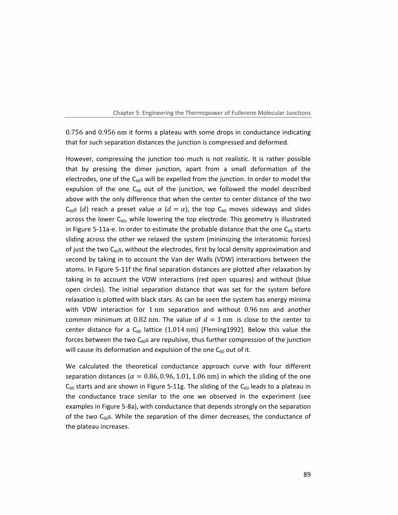
Chapter 5: Engineering the Thermopower of Fullerene Molecular Junctions
89
0.756 and 0.956nm it forms a plateau with some drops in conductance indicating
that for such separation distances the junction is compressed and deformed.
However, compressing the junction too much is not realistic. It is rather possible
that by pressing the dimer junction, apart from a small deformation of the
electrodes, one of the C60s will be expelled from the junction. In order to model the
expulsion of the one C60 out of the junction, we followed the model described
above with the only difference that when the center to center distance of the two
C60s (�) reach a preset value � (� = �), the top C60 moves sideways and slides
across the lower C60, while lowering the top electrode. This geometry is illustrated
in Figure 5-11a-e. In order to estimate the probable distance that the one C60 starts
sliding across the other we relaxed the system (minimizing the interatomic forces)
of just the two C60s, without the electrodes, first by local density approximation and
second by taking in to account the Van der Walls (VDW) interactions between the
atoms. In Figure 5-11f the final separation distances are plotted after relaxation by
taking in to account the VDW interactions (red open squares) and without (blue
open circles). The initial separation distance that was set for the system before
relaxation is plotted with black stars. As can be seen the system has energy minima
with VDW interaction for 1nm separation and without 0.96nm and another
common minimum at 0.82nm. The value of � = 1nm is close to the center to
center distance for a C60 lattice (1.014nm) [Fleming1992]. Below this value the
forces between the two C60s are repulsive, thus further compression of the junction
will cause its deformation and expulsion of the one C60 out of it.
We calculated the theoretical conductance approach curve with four different
separation distances (� = 0.86, 0.96, 1.01, 1.06nm) in which the sliding of the one
C60 starts and are shown in Figure 5-11g. The sliding of the C60 leads to a plateau in
the conductance trace similar to the one we observed in the experiment (see
examples in Figure 5-8a), with conductance that depends strongly on the separation
of the two C60s. While the separation of the dimer decreases, the conductance of
the plateau increases.
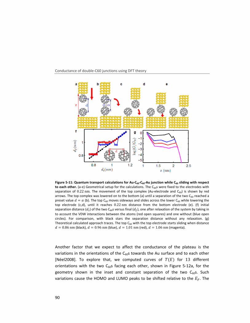
Conductance of double-C60 junctions using DFT theory
90
Figure 5-11: Quantum transport calculations for Au-C60-C60-Au junction while C60 sliding with respect
to each other. (a-e) Geometrical setup for the calculations. The C60s were fixed to the electrodes with separation of 0.22nm. The movement of the top complex (Au-electrode and C60) is shown by red arrows. The top complex was lowered on to the bottom (a) until a separation of the two C60 reached a preset value � = � (b). The top C60 moves sideways and slides across the lower C60 while lowering the top electrode (c,d), until it reaches 0.22nm distance from the bottom electrode (e). (f) initial separation distance (��) of the two C60s versus final (�w), one after relaxation of the system by taking in
to account the VDW interactions between the atoms (red open squares) and one without (blue open circles). For comparison, with black stars the separation distance without any relaxation. (g) Theoretical calculated approach traces. The top C60 with the top electrode starts sliding when distance � = 0.86nm (black), � = 0.96nm (blue), � = 1.01nm (red), � = 1.06nm (magenta).
Another factor that we expect to affect the conductance of the plateau is the
variations in the orientations of the C60s towards the Au surface and to each other
[Néel2008]. To explore that, we computed curves of �(+) for 13 different
orientations with the two C60s facing each other, shown in Figure 5-12a, for the
geometry shown in the inset and constant separation of the two C60s. Such
variations cause the HOMO and LUMO peaks to be shifted relative to the +8. The
Chapter 5: Engineering the Thermopower of Fullerene Molecular Junctions
91
conductance values for the +8 obtained from the DFT calculations can vary more
than two orders of magnitude.
Figure 5-12: Quantum transport calculations for Au-C60-C60-Au junction for different orientations of
the C60s. (a) Transmission curves for the geometry shown in the inset for 13 different orientations of the two C60s facing each other. The black vertical dashed line indicates the position of Fermi energy obtained by DFT. (b,c) Theoretical calculated approach traces for the geometry of Figure 5-11a-e for two different orientations of the two C60s facing each other before starting sliding: (b) Hexagon – hexagon and (c) hexagon-atom. (d) Experimental approach trace of a C60 tip on an isolated individual C60.
We calculated the theoretical conductance approach trace for the geometry shown
in Figure 5-11a-e for two different orientations of the two C60s facing each other
before starting sliding at separation distance � = 1.01nm. In Figure 5-12b they
initially face each other with atom-hexagon and in Figure 5-12c with hexagon-
hexagon. By changing the initial facing orientation, the whole facing orientation
during the sliding of the two C60s will change and thus the conductance plateau will
Simultaneous S and G measurements of single- and double-C60 junctions
92
be different. Although these calculations overestimate the values for the
conductance, they do reproduce the experimental trends as can be seen from the
experimental approach curve shown in Figure 5-12d.
In conclusion the DFT calculations show that the conductance of a Au-C60-C60-Au
junction can vary up to two orders of magnitude depending on the orientation of
the molecules and the two C60s separation distance in agreement with the high
dispersion of conductance values of the shoulder on the experimental 2D-
histogram.
5.3 Simultaneous S and G measurements of single- and
double-C60 junctions
Thermopower of C60s sandwiched between gold substrate and Pt, Au, and Ag tips
have been reported by Yee et al [Yee2011]. Their technique is described in chapter
4. They measure the thermopower just at one specific point during the evolution of
the junction and reported an average thermopower value. In contrast to these
experiments, with our technique we are able to measure thermopower and
conductance simultaneously during the whole evolution of the molecular junction,
thereby achieving a complete characterization at the single molecule level.
Once we target an isolated individual molecule we start the approach of the tip, and
the motion is stopped at fixed intervals of 20 − 30pm. The bias voltage is
maintained at 100mV during the tip motion and swept between ±5mV ( − �
curve) while the tip is stationary. In each approach − retraction cycle, 50 − 100
− � traces are acquired. We have measured the thermopower at two
temperature differences between the tip and the sample �� = 12K and 25K for
a total of 119 single-C60 junctions (61 at �� = 12K and 58 at �� = 25K) and 23
C60 dimers (8 at �� = 12K and 15 at �� = 25K). Further details on the
technique can be found in chapter 4
Chapter 5: Engineering the Thermopower of Fullerene Molecular Junctions
93
In Figure 5-13a-h, we show four examples of conductance and thermopower
approach - retraction traces measured simultaneously on a single C60 molecule.
Figure 5-13a,c,e,g shows the conductance (blue) and thermopower (green)
approach traces and Figure 5-13b,d,f,h the corresponding conductance (red) and
thermopower (magenta) retraction traces. Contact formation in the approach
curves is clearly indicated by the abrupt jump (see Figure 5-13c,e,g) or change of
slope (see Figure 5-13a) in the conductance which results in an abrupt jump in the
thermopower. The subsequent jumps in the conductance observed in conductance
due to the atomic rearrangements are also reflected in jumps in the thermopower,
demonstrating the sensitivity of thermopower to atomic details. During retraction
the curves remain almost the same indicating that the junction was unaltered.
In Figure 5-15a,b we plotted the 2D-historgram of the thermopower with
conductance for temperature difference of �� = 12K and �� = 25K
respectively, which gives information on the probability of a thermopower values to
appear at certain conductance values.
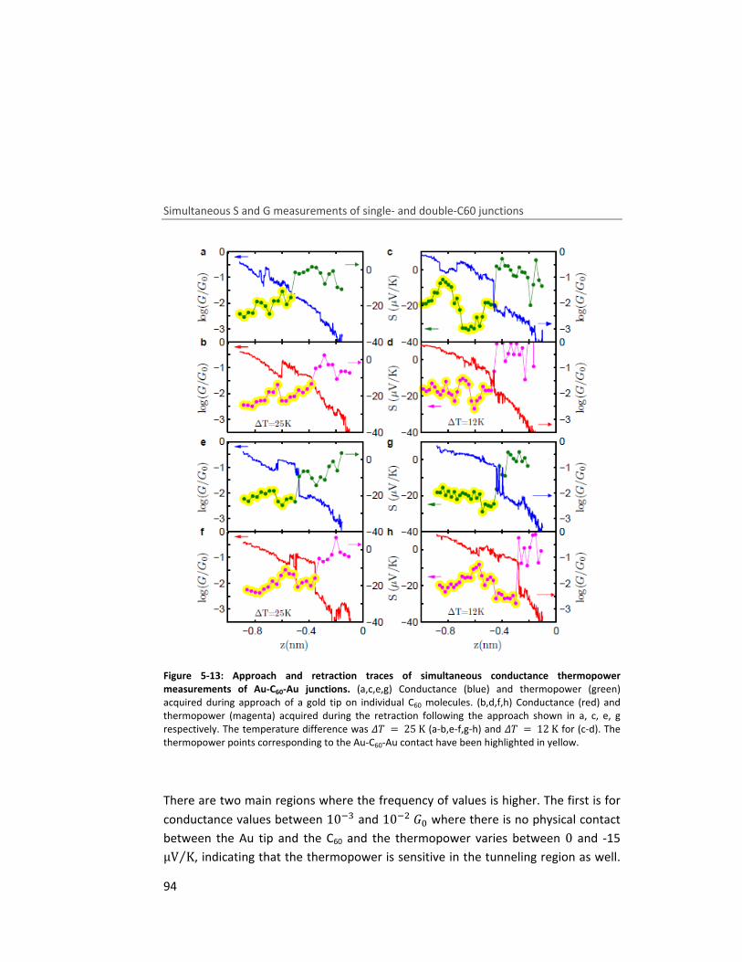
Simultaneous S and G measurements of single- and double-C60 junctions
94
Figure 5-13: Approach and retraction traces of simultaneous conductance thermopower
measurements of Au-C60-Au junctions. (a,c,e,g) Conductance (blue) and thermopower (green) acquired during approach of a gold tip on individual C60 molecules. (b,d,f,h) Conductance (red) and thermopower (magenta) acquired during the retraction following the approach shown in a, c, e, g respectively. The temperature difference was �� = 25K (a-b,e-f,g-h) and �� = 12K for (c-d). The thermopower points corresponding to the Au-C60-Au contact have been highlighted in yellow.
There are two main regions where the frequency of values is higher. The first is for
conductance values between 10�N and 10��� where there is no physical contact
between the Au tip and the C60 and the thermopower varies between 0 and -15 μV K⁄ , indicating that the thermopower is sensitive in the tunneling region as well.
Chapter 5: Engineering the Thermopower of Fullerene Molecular Junctions
95
The second region is for conductance values higher than 10�'� corresponding to
the Au-C60-Au junction and thermopower is higher, up to −40 μV K⁄ . Between
these two regions there is a transition region for conductance between 10�� and 10�'� where the thermopower increases. This is the region where the contact of
the Au tip with the C60 is formed.
In Figure 5-14a-h, we show three examples of conductance and thermopower
approach-retraction traces measured simultaneously on a C60 dimer. Figure
5-14a,c,e,g shows the conductance (blue) and thermopower (green) approach
traces and Figure 5-14b,d,f,h the corresponding conductance (red) and
thermopower (magenta) retraction traces. The formation of the dimer is clearly
identified by the already mentioned shoulder in the conductance. We can observe
that a corresponding shoulder is present in the thermopower with values in the
range of −25to−50μV/K for these particular dimers. On the characteristic
shoulder some drops in the conductance appear while squeezing the junction and
the two C60s are sliding with respect to each other. These drops are also reflected in
the thermopower (see Figure 5-14e) indicating the sensitivity of thermopower on
the coupling of the dimer. When the one C60 is expelled from the junction the
conductance drops with a subsequent increase up to the formation of an Au-C60-Au
junction indicated by the abrupt jump or change of slope while the thermopower
drops to low values (0 − 10μV/K) and remains constant up to the formation of the
Au-C60-Au junction where it increases up to −30μV/K for the specific examples in
Figure 5-14a,e. In example Figure 5-14c,d we retract before forming the Au-C60-Au
junction. In most cases the retraction curves of conductance and thermopower are
the typical retraction curves we observed for an Au-C60-Au junction (Figure 5-14b,f).
In some cases the retraction conductance curve presents the same characteristic
shoulder as the approach curve indicating that the expelled C60 reenters the
junction. Similarly the characteristic shoulder exists on the thermopower curve
(Figure 5-14d,h).
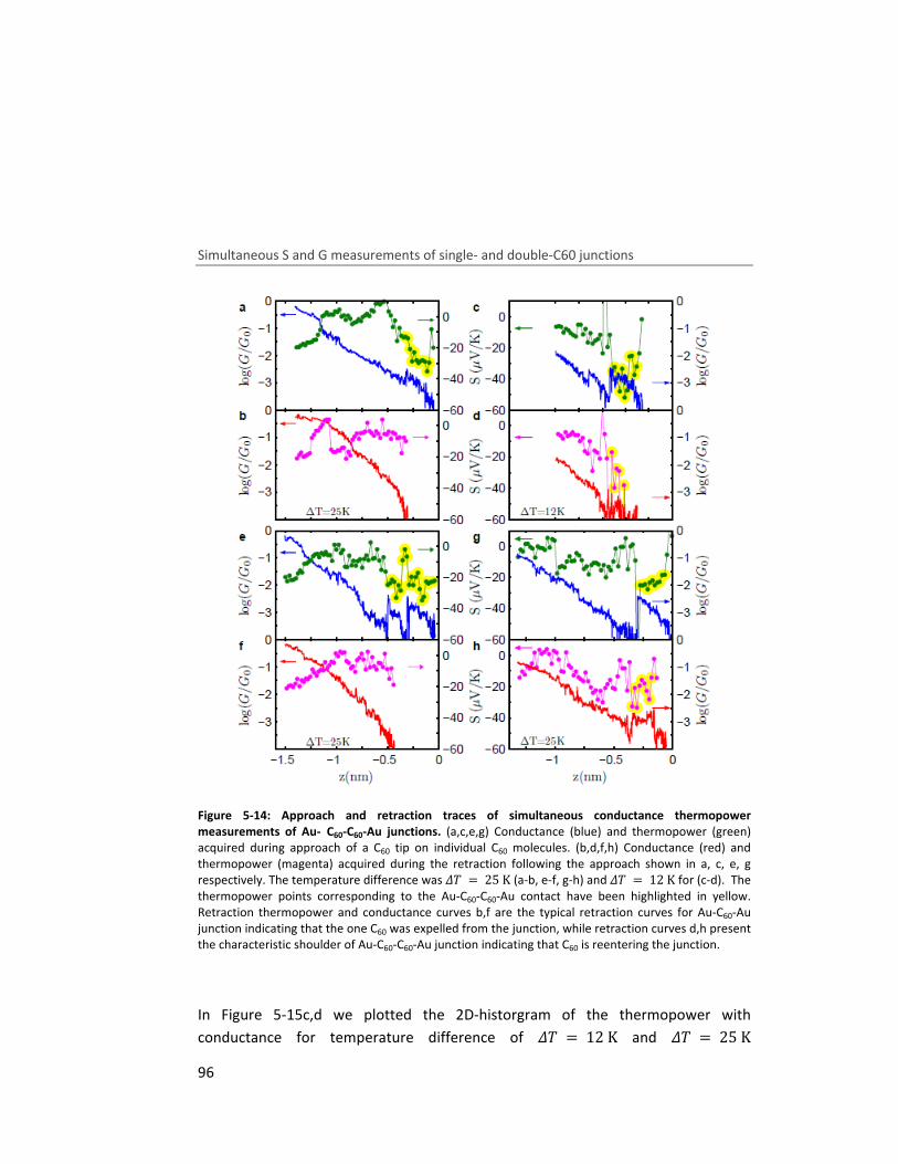
Simultaneous S and G measurements of single- and double-C60 junctions
96
Figure 5-14: Approach and retraction traces of simultaneous conductance thermopower
measurements of Au- C60-C60-Au junctions. (a,c,e,g) Conductance (blue) and thermopower (green) acquired during approach of a C60 tip on individual C60 molecules. (b,d,f,h) Conductance (red) and thermopower (magenta) acquired during the retraction following the approach shown in a, c, e, g respectively. The temperature difference was �� = 25K (a-b, e-f, g-h) and �� = 12K for (c-d). The thermopower points corresponding to the Au-C60-C60-Au contact have been highlighted in yellow. Retraction thermopower and conductance curves b,f are the typical retraction curves for Au-C60-Au junction indicating that the one C60 was expelled from the junction, while retraction curves d,h present the characteristic shoulder of Au-C60-C60-Au junction indicating that C60 is reentering the junction.
In Figure 5-15c,d we plotted the 2D-historgram of the thermopower with
conductance for temperature difference of �� = 12K and �� = 25K
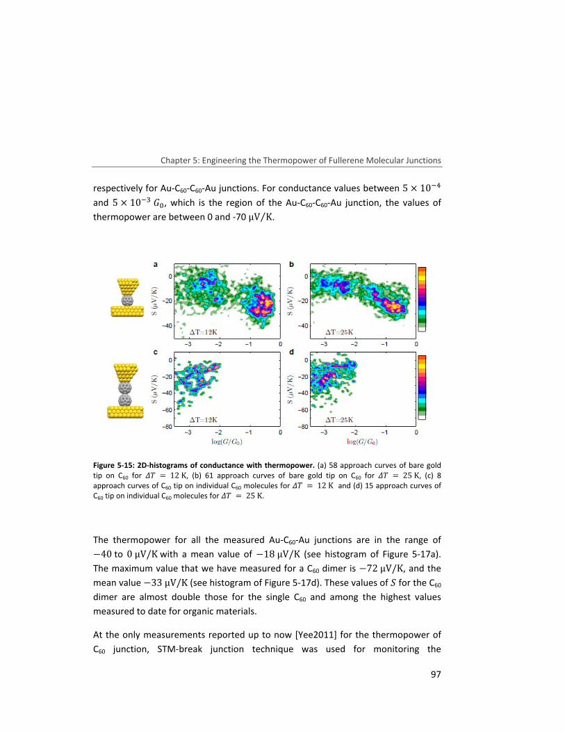
Chapter 5: Engineering the Thermopower of Fullerene Molecular Junctions
97
respectively for Au-C60-C60-Au junctions. For conductance values between 5 × 10�Ó
and 5 × 10�N� , which is the region of the Au-C60-C60-Au junction, the values of
thermopower are between 0 and -70 μV K⁄ .
Figure 5-15: 2D-histograms of conductance with thermopower. (a) 58 approach curves of bare gold tip on C60 for �� = 12K, (b) 61 approach curves of bare gold tip on C60 for �� = 25K, (c) 8 approach curves of C60 tip on individual C60 molecules for �� = 12K and (d) 15 approach curves of C60 tip on individual C60 molecules for �� = 25K.
The thermopower for all the measured Au-C60-Au junctions are in the range of −40to 0μV/Kwith a mean value of −18μV/K (see histogram of Figure 5-17a).
The maximum value that we have measured for a C60 dimer is −72μV/K, and the
mean value −33μV/K (see histogram of Figure 5-17d). These values of � for the C60
dimer are almost double those for the single C60 and among the highest values
measured to date for organic materials.
At the only measurements reported up to now [Yee2011] for the thermopower of
C60 junction, STM-break junction technique was used for monitoring the
Simultaneous S and G measurements of single- and double-C60 junctions
98
conductance, and the thermopower was measured at one specific point during the
evolution of the junction. Due to the uncertainty in the number of molecules
participating in the junction, they used statistical analysis to obtain the most
probable conductance and thermopower value (5 × 10�Ó� and −14.5μV/K
respectively). In contrast, we measured the conductance and thermopower of
single- and double-C60 junctions during the whole evolution of the junction. The
mean thermopower value for single-C60 junctions we observed is somewhat higher,
while the conductance is more than two orders of magnitude higher than their
value. The mean conductance and thermopower that they observed is an average
for junctions with different number of C60s. Formation of junctions with more than
one C60 is possible since there is no control on the number of molecules
participating in the junction in contrast to our approach, where we can distinguish
the different junctions.
Further DFT calculations were performed by Prof. C.J. Lambert’s group, for better
understanding of the thermopower of single- and double-C60 junctions. An example
of theoretical approach conductance and thermopower trace of single- and double-
C60 junction is shown in Figure 5-16b,e respectively. For comparison, experimentally
obtained curves are also plotted in Figure 5-16a,d. The theoretical approach curves
indeed reproduce the characteristic trends of the experimentally observed ones for
single- and double-C60 junctions. In addition Figure 5-16c,f shows curves of the
figure of merit �, which are inaccessible in our experiments.

Chapter 5: Engineering the Thermopower of Fullerene Molecular Junctions
99
Figure 5-16: DFT calculated results of thermopower and figure of merit for single- and double-C60
junctions. (a) Conductance at 100 mV (blue) and thermopower (magenta), simultaneously acquired, for approach on a single C60 molecule. In this measurement the temperature difference was �� = 25K. The shaded area indicates the range of ¿ for which the Au−C60−Au junction is already formed. (b) Theoretical conductance (blue) and thermopower versus distance for a single C60. (c) Calculated figure of merit � for a single C60. (d) Conductance at 100 mV (blue) and thermopower (magenta), simultaneously acquired, during the formation of the C60 dimer. In this measurement, the temperature difference was �� = 12K. The shaded area indicates the range in which the C60 dimer is in the junction. (e) Theoretical conductance (blue) and thermopower versus distance for the C60 dimer. (f) Calculated figure of merit ZT for a C60 dimer.
In addition to the single- and double-C60 junctions, in the theoretical calculations,
the thermopower values for a triple C60 junction were extracted. For single-, double-
and triple-C60 junctions Figure 5-17b,e,g shows the histograms from these
theoretical curves across a range of electrode separations and a range of different
positions for the Fermi energy. Further information on the construction of the
histograms can be found in ref. [Evangeli2013]. Although these calculations
overestimate the values for the thermopower and the conductance, they do
reproduce the experimental trends and support all the main conclusions from the
experiments. The main discrepancy with the experiment is associated with
uncertainty in the junction geometry, since the precise atomic-scale configuration
Simultaneous S and G measurements of single- and double-C60 junctions
100
of the electrodes is not known and is likely to vary both between and along pulling
curves.
The theoretical calculations also found that the average thermopower for a chain of
two C60s is approximately 100% higher than that of a single C60 with a further
doubling predicted for a chain of three C60s. From the theoretical histograms of
Figure 5-17c,f,h, we find that the average value for � is also enhanced by
introducing more on-the-tip C60s and tuning the coupling between them. For a
single C60, theoretical calculations predict the average � = 0.1, for two C60s � = 0.4, while for the 3 C60s � = 1.65, which represents a 4-fold and a 16-fold
increase, respectively. This suggests that C60 films with weakly coupled layers have
the potential to be competitive with the best available values for inorganic
materials, although it should be noted that the predictions for � include only the
electronic contribution to the thermal conductance, which ignores parasitic
contributions from phonons and therefore represents an upper bound.
In agreement with refs [Malen2010] and [Dubi2011], the relative fluctuation in the
thermopower is found to be smaller than that of the conductance and,
furthermore, this trend becomes more pronounced for multi-C60 junctions. For
example for the C60 dimer, experimentally, we find ¬� �⁄ = 0.36, whereas ¬� �⁄ = 1.2 and theoretically for a triple-C60s ¬� �⁄ = 0.62, and ¬� �⁄ = 5,
where ¬� and ¬� are the standard deviations and � and � the mean values. Since
the sensitivity of � to atomic-scale fluctuations is lower than that of electrical
conductance, thermopower is a particularly attractive property for investigation
and optimization at a molecular scale.
The increase in the thermopower observed by tuning the intermolecular coupling
between identical molecules differs from various intramolecular approaches to
tuning � reported up to now, including varying the chemical
composition,[Baheti2008] varying the position of intramolecular energy levels
relative to the work function of metallic electrodes,[Yee2010; Yee2011]
systematically increasing the single molecule lengths within a family of
molecules,[Malen2009] and systematically varying the conformation of molecules
[Finch2009].

Chapter 5: Engineering the Thermopower of Fullerene Molecular Junctions
101
Figure 5-17: Histograms of thermopower obtained experimentally and with DFT calculations. (a) Histogram of experimental thermopower values at contact for a single C60 molecule, measured at �� = 12K (blue) and25K (red). (b,c) Histograms of the theoretically computed thermopower and figure of merit, respectively, for a single C60. (d) Histogram of experimental thermopower values at contact for a C60 dimer, measured at �� = 12K (blue) and 25K (red). (e,f) Histograms of the theoretically computed thermopower (e) and figure of merit (f), respectively, for a C60 dimer. (g,h) Histograms of the theoretically computed thermopower (g) and figure of merit (h) for a C60 trimer. � is the mean value of the thermopower, ¬� is the standard deviation.
Conclusions
102
5.4 Conclusions
In this chapter we studied the thermopower and conductance of C60 junctions. In
contrast to previously reported experimental results, by imaging the sample prior to
junction formation, the exact number of molecules in the junction is known. We
formed single- and double-C60 junctions controllably and we measured
simultaneously, the thermopower and conductance during the whole evolution of
the junction. We observed that the thermopower of a C60 molecule can be doubled
by coupling two C60 molecules. DFT-based calculations by Prof. C.J. Lambert’s group
show that the thermopower can be further doubled by coupling to a third C60. The
figure of merit � shows a 4-fold and a 16-fold increase, for two and three C60s
respectively with respect to one C60. Our results demonstrate the possibility of
engineering the thermopower of a molecular junction by mechanical manipulation.
Chapter 5: Engineering the Thermopower of Fullerene Molecular Junctions
103
References
[Agraït1995] Agraït, N., G. Rubio and S. Vieira (1995). "Plastic Deformation of
Nanometer-Scale Gold Connective Necks." Physical Review Letters 74(20): 3995-3998.
[Agraït1996] Agraït, N., G. Rubio and S. Vieira (1996). "Plastic Deformation in Nanometer Scale Contacts†." Langmuir 12(19): 4505-4509.
[Alexandre2005] Alexandre, R. R., M. G.-s. Víctor, W. B. Steve, J. L. Colin, F. Jaime, et al. (2005). "Towards molecular spintronics." Nature Materials 4(4): 335-339.
[Arnau2011] Arnau, A., R. Berndt, T. Frederiksen, G. Schull and D. Sánchez-Portal (2011). "Atomic-scale engineering of electrodes for single-molecule contacts." Nature Nanotechnology 6: 23-27.
[Arroyo2011] Arroyo, C. R., E. Leary, A. Castellanos-Gómez, G. Rubio-Bollinger, M. T. González, et al. (2011). "Influence of Binding Groups on Molecular Junction Formation." Journal of the American Chemical Society 133(36): 14313-14319.
[Baheti2008] Baheti, K., J. A. Malen, P. Doak, P. Reddy, S.-Y. Jang, et al. (2008). "Probing the Chemistry of Molecular Heterojunctions Using Thermoelectricity." Nano Letters 8(2): 715-719.
[Böhler2007] Böhler, T., A. Edtbauer and E. Scheer (2007). "Conductance of individual C_{60} molecules measured with controllable gold electrodes." Physical Review B 76(12): 125432.
[Chen2005] Chen, F., J. He, C. Nuckolls, T. Roberts, J. E. Klare, et al. (2005). "A Molecular Switch Based on Potential-Induced Changes of Oxidation State." Nano Letters 5(3): 503-506.
[Cheng2011] Cheng, Z. L., SkoutaR, VazquezH, J. R. Widawsky, SchneebeliS, et al. (2011). "In situ formation of highly conducting covalent Au-C contacts for single-molecule junctions." Nat Nano 6(6): 353-357.
[Dubi2011] Dubi, Y. and M. Di Ventra (2011). "Colloquium: Heat flow and thermoelectricity in atomic and molecular junctions." Reviews of Modern Physics 83(1): 131-155.
[Evangeli2013] Evangeli, C., K. Gillemot, E. Leary, M. T. González, G. Rubio-Bollinger, et al. (2013). "Engineering the Thermopower of C60 Molecular Junctions." Nano Letters 13(5): 2141-2145.
[Finch2009] Finch, C. M., V. M. García-Suárez and C. J. Lambert (2009). "Giant thermopower and figure of merit in single-molecule devices." Physical Review B 79(3): 033405.
References
104
[Fleming1992] Fleming, R. M., B. Hessen, T. Siegrist, A. R. Kortan, P. Marsh, et al. (1992). Crystalline Fullerenes. Fullerenes, American Chemical Society. 481:
25-39. [Franke2009] Franke, K. J., G. Schulze and J. I. Pascual (2009). "Excitation of
Jahn−Teller Acfve Modes during Electron Transport through Single C60 Molecules on Metal Surfaces." The Journal of Physical Chemistry Letters 1(2): 500-504.
[French2012] French, W. R., C. R. Iacovella and P. T. Cummings (2012). "Large-Scale Atomistic Simulations of Environmental Effects on the Formation and Properties of Molecular Junctions." ACS Nano 6(3): 2779-2789.
[Gardener2009] Gardener, J. A., G. A. D. Briggs and M. R. Castell (2009). "Scanning tunneling microscopy studies of C_{60} monolayers on Au(111)." Physical Review B 80(23): 235434.
[González2006] González, M. T., S. Wu, R. Huber, S. J. van der Molen, C. Schönenberger, et al. (2006). "Electrical Conductance of Molecular Junctions by a Robust Statistical Analysis." Nano Letters 6(10): 2238-2242.
[Guldi2000] Guldi, D. M. and M. Prato (2000). "Excited-State Properties of C60 Fullerene Derivatives." Accounts of Chemical Research 33(10): 695-703.
[Hahn1998] Hahn, J. R., Y. A. Hong and H. Kang (1998). "Electron tunneling across an interfacial water layer inside an STM junction: tunneling distance, barrier height and water polarization effect." Applied Physics A 66(1): S467-S472.
[Hauptmann2012] Hauptmann, N., F. Mohn, L. Gross, G. Meyer, T. Frederiksen, et al. (2012). "Force and conductance during contact formation to a C60 molecule." New J. Phys 14.
[Huber2007] Huber, R., M. T. González, S. Wu, M. Langer, S. Grunder, et al. (2007). "Electrical Conductance of Conjugated Oligomers at the Single Molecule Level." Journal of the American Chemical Society 130(3): 1080-1084.
[Joachim1995] Joachim, C., J. K. Gimzewski, R. R. Schlittler and C. Chavy (1995). "Electronic Transparence of a Single C_{60} Molecule." Physical Review Letters 74(11): 2102-2105.
[Langa2007] Langa, F., J. F. Nierengarten and R. S. o. Chemistry (2007). Fullerenes: Principles and Applications, Royal Society of Chemistry.
[Malen2009] Malen, J. A., P. Doak, K. Baheti, T. D. Tilley, A. Majumdar, et al. (2009). "The Nature of Transport Variations in Molecular Heterojunction Electronics." Nano Letters 9(10): 3406-3412.
[Malen2010] Malen, J. A., S. K. Yee, A. Majumdar and R. A. Segalman (2010). "Fundamentals of energy transport, energy conversion, and thermal
Chapter 5: Engineering the Thermopower of Fullerene Molecular Junctions
105
properties in organic–inorganic heterojunctions." Chemical Physics Letters 491(4–6): 109-122.
[Moreno-García2013] Moreno-García, P., M. Gulcur, D. Z. Manrique, T. Pope, W. Hong, et al. (2013). "Single-Molecule Conductance of Functionalized Oligoynes: Length Dependence and Junction Evolution." Journal of the American Chemical Society 135(33): 12228-12240.
[Néel2007] Néel, N., J. Kröger, L. Limot, T. Frederiksen, M. Brandbyge, et al. (2007). "Controlled Contact to a C_{60} Molecule." Physical Review Letters 98(6): 065502.
[Néel2008] Néel, N., J. r. Kröger, L. Limot and R. Berndt (2008). "Conductance of Oriented C60 Molecules." Nano Letters 8(5): 1291-1295.
[Nishino2005] Nishino, T., T. Ito and Y. Umezawa (2005). "A fullerene molecular tip can detect localized and rectified electron tunneling within a single fullerene–porphyrin pair." Proceedings of the National Academy of Sciences of the United States of America 102(16): 5659-5662.
[Qiao2007] Qiao, R., A. P. Roberts, A. S. Mount, S. J. Klaine and P. C. Ke (2007). "Translocation of C60 and Its Derivatives Across a Lipid Bilayer." Nano Letters 7(3): 614-619.
[Repp2005] Repp, J., G. Meyer, S. M. Stojković, A. Gourdon and C. Joachim (2005). "Molecules on Insulating Films: Scanning-Tunneling Microscopy Imaging of Individual Molecular Orbitals." Physical Review Letters 94(2): 026803.
[Reuter2012] Reuter, M. G., M. C. Hersam, T. Seideman and M. A. Ratner (2012). "Signatures of Cooperative Effects and Transport Mechanisms in Conductance Histograms." Nano Letters 12(5): 2243-2248.
[Reuter2011] Reuter, M. G., T. Seideman and M. A. Ratner (2011). "Molecular Conduction through Adlayers: Cooperative Effects Can Help or Hamper Electron Transport." Nano Letters 11(11): 4693-4696.
[Rocha2006] Rocha, A. R., V. M. García-Suárez, S. Bailey, C. Lambert, J. Ferrer, et al. (2006). "Spin and molecular electronics in atomically generated orbital landscapes." Physical Review B 73(8): 085414.
[Rubio1996] Rubio, G., N. Agraït and S. Vieira (1996). "Atomic-Sized Metallic Contacts: Mechanical Properties and Electronic Transport." Physical Review Letters 76(13): 2302-2305.
[Schull2009] Schull, G., T. Frederiksen, M. Brandbyge and R. Berndt (2009). "Passing Current through Touching Molecules." Physical Review Letters 103(20): 206803.
References
106
[Schulze2008] Schulze, G., K. J. Franke, A. Gagliardi, G. Romano, C. S. Lin, et al. (2008). "Resonant Electron Heating and Molecular Phonon Cooling in Single C_{60} Junctions." Physical Review Letters 100(13): 136801.
[Soler2002] Soler, J. M., E. Artacho, J. D. Gale, A. García, J. Junquera, et al. (2002). "The SIESTA method for ab initio order-N materials simulation." J. Phys.: Condens. Matter 14(2745).
[Songmei2008] Songmei, W., G. Maria Teresa, H. Roman, G. Sergio, M. Marcel, et al. (2008). "Molecular junctions based on aromatic coupling." Nature Nanotechnology 3(9): 569-574.
[Tang2011] Tang, L., Y. Xie and Q. Guo (2011). "Complex orientational ordering of C60 molecules on Au(111)." The Journal of Chemical Physics 135(11): -.
[van Ruitenbeek1996] van Ruitenbeek, J. M., A. Alvarez, I. Piñeyro, C. Grahmann, P. Joyez, et al. (1996). "Adjustable nanofabricated atomic size contacts." Review of Scientific Instruments 67(1): 108-111.
[Wiesendanger1994] Wiesendanger, R. (1994). Scanning Probe Microscopy and Spectroscopy: Methods and Applications, Cambridge University Press.
[Xu2003] Xu, B. and N. J. Tao (2003). "Measurement of Single-Molecule Resistance by Repeated Formation of Molecular Junctions." Science 301(5637): 1221-1223.
[Yee2010] Yee, S., J. Malen, P. Reddy, R. Segalman and M. A. (2010). "Thermoelectricity at the Organic-Inorganic Interface." Proceedings of the 14th International Heat Transfer Conference IHTC14, Washington, DC, August 7−13, 2010 IHTC14-22690: 845-855.
[Yee2011] Yee, S. K., J. A. Malen, A. Majumdar and R. A. Segalman (2011). "Thermoelectricity in Fullerene–Metal Heterojunctions." Nano Letters 11(10): 4089-4094.
The advent of experimental techniques like the STM and the mechanically
controlled break junctions (MCBJs) has allowed investigation of the transport
properties of metallic atomic
be ideal systems where quantum theories of charge and energy transport have
been thoroughly tested
has received little attention so far due to experimental challenges and it is still
unclear what determines the thermoelectricity in a metallic atomic
[Ludoph1999
ato
conductance. We show that the thermopower in the nanoscale is governed by
quantum effects that are radically different from the mechanisms that govern
thermoelectrics in macroscopi
6.1
As seen in
qualitatively understood since the pioneering work of Sir N. F. Mott
sign and magnitude (
conductivity around the Fermi energy, which in turn depends on the inelastic
relaxation time and the effective mass. Thus
magnitude and negative sign of the thermopower of transition metals (like Ni, Pd or
Pt) is attribute
The advent of experimental techniques like the STM and the mechanically
controlled break junctions (MCBJs) has allowed investigation of the transport
properties of metallic atomic
be ideal systems where quantum theories of charge and energy transport have
been thoroughly tested
has received little attention so far due to experimental challenges and it is still
unclear what determines the thermoelectricity in a metallic atomic
Ludoph1999]. In this chapter we
atomic metallic contacts by measuring simultaneously thermopower and
conductance. We show that the thermopower in the nanoscale is governed by
quantum effects that are radically different from the mechanisms that govern
thermoelectrics in macroscopi
6.1 Introduction
As seen in chapter
qualitatively understood since the pioneering work of Sir N. F. Mott
sign and magnitude (
nductivity around the Fermi energy, which in turn depends on the inelastic
relaxation time and the effective mass. Thus
magnitude and negative sign of the thermopower of transition metals (like Ni, Pd or
Pt) is attribute
The advent of experimental techniques like the STM and the mechanically
controlled break junctions (MCBJs) has allowed investigation of the transport
properties of metallic atomic
be ideal systems where quantum theories of charge and energy transport have
been thoroughly tested [Agraıt2003
has received little attention so far due to experimental challenges and it is still
unclear what determines the thermoelectricity in a metallic atomic
. In this chapter we
mic metallic contacts by measuring simultaneously thermopower and
conductance. We show that the thermopower in the nanoscale is governed by
quantum effects that are radically different from the mechanisms that govern
thermoelectrics in macroscopi
Introduction
chapter 2 the room temperature thermopower in bulk metals is
qualitatively understood since the pioneering work of Sir N. F. Mott
sign and magnitude (0 � 10nductivity around the Fermi energy, which in turn depends on the inelastic
relaxation time and the effective mass. Thus
magnitude and negative sign of the thermopower of transition metals (like Ni, Pd or
Pt) is attributed to the increasing relaxation time with energy due to their
Chapter 6: Quantum Thermopower of Metallic Nanocontacts
The advent of experimental techniques like the STM and the mechanically
controlled break junctions (MCBJs) has allowed investigation of the transport
properties of metallic atomic-size contacts
be ideal systems where quantum theories of charge and energy transport have
Agraıt2003]. However, thermoelectricity in these contacts
has received little attention so far due to experimental challenges and it is still
unclear what determines the thermoelectricity in a metallic atomic
. In this chapter we study the thermopower of gold and pl
mic metallic contacts by measuring simultaneously thermopower and
conductance. We show that the thermopower in the nanoscale is governed by
quantum effects that are radically different from the mechanisms that govern
thermoelectrics in macroscopic systems.
he room temperature thermopower in bulk metals is
qualitatively understood since the pioneering work of Sir N. F. Mott 10μV/K) depend on the energy dependence of the
nductivity around the Fermi energy, which in turn depends on the inelastic
relaxation time and the effective mass. Thus
magnitude and negative sign of the thermopower of transition metals (like Ni, Pd or
d to the increasing relaxation time with energy due to their
Quantum Thermopower of Metallic Nanocontacts
The advent of experimental techniques like the STM and the mechanically
controlled break junctions (MCBJs) has allowed investigation of the transport
size contacts. These atomic wires have turned out to
be ideal systems where quantum theories of charge and energy transport have
. However, thermoelectricity in these contacts
has received little attention so far due to experimental challenges and it is still
unclear what determines the thermoelectricity in a metallic atomic
study the thermopower of gold and pl
mic metallic contacts by measuring simultaneously thermopower and
conductance. We show that the thermopower in the nanoscale is governed by
quantum effects that are radically different from the mechanisms that govern
c systems.
he room temperature thermopower in bulk metals is
qualitatively understood since the pioneering work of Sir N. F. Mott
) depend on the energy dependence of the
nductivity around the Fermi energy, which in turn depends on the inelastic
relaxation time and the effective mass. Thus, for instance, the relatively large
magnitude and negative sign of the thermopower of transition metals (like Ni, Pd or
d to the increasing relaxation time with energy due to their
Quantum Thermopower of Metallic Nanocontacts
The advent of experimental techniques like the STM and the mechanically
controlled break junctions (MCBJs) has allowed investigation of the transport
. These atomic wires have turned out to
be ideal systems where quantum theories of charge and energy transport have
. However, thermoelectricity in these contacts
has received little attention so far due to experimental challenges and it is still
unclear what determines the thermoelectricity in a metallic atomic
study the thermopower of gold and pl
mic metallic contacts by measuring simultaneously thermopower and
conductance. We show that the thermopower in the nanoscale is governed by
quantum effects that are radically different from the mechanisms that govern
he room temperature thermopower in bulk metals is
qualitatively understood since the pioneering work of Sir N. F. Mott
) depend on the energy dependence of the
nductivity around the Fermi energy, which in turn depends on the inelastic
for instance, the relatively large
magnitude and negative sign of the thermopower of transition metals (like Ni, Pd or
d to the increasing relaxation time with energy due to their
Quantum Thermopower of Metallic Nanocontacts
The advent of experimental techniques like the STM and the mechanically
controlled break junctions (MCBJs) has allowed investigation of the transport
. These atomic wires have turned out to
be ideal systems where quantum theories of charge and energy transport have
. However, thermoelectricity in these contacts
has received little attention so far due to experimental challenges and it is still
unclear what determines the thermoelectricity in a metallic atomic-size contact
study the thermopower of gold and platinum
mic metallic contacts by measuring simultaneously thermopower and
conductance. We show that the thermopower in the nanoscale is governed by
quantum effects that are radically different from the mechanisms that govern
he room temperature thermopower in bulk metals is
qualitatively understood since the pioneering work of Sir N. F. Mott [Mott1936
) depend on the energy dependence of the
nductivity around the Fermi energy, which in turn depends on the inelastic
for instance, the relatively large
magnitude and negative sign of the thermopower of transition metals (like Ni, Pd or
d to the increasing relaxation time with energy due to their
Quantum Thermopower of Metallic Nanocontacts
107
The advent of experimental techniques like the STM and the mechanically
controlled break junctions (MCBJs) has allowed investigation of the transport
. These atomic wires have turned out to
be ideal systems where quantum theories of charge and energy transport have
. However, thermoelectricity in these contacts
has received little attention so far due to experimental challenges and it is still
e contact
atinum
mic metallic contacts by measuring simultaneously thermopower and
conductance. We show that the thermopower in the nanoscale is governed by
quantum effects that are radically different from the mechanisms that govern
he room temperature thermopower in bulk metals is
Mott1936]. Its
) depend on the energy dependence of the
nductivity around the Fermi energy, which in turn depends on the inelastic
for instance, the relatively large
magnitude and negative sign of the thermopower of transition metals (like Ni, Pd or
d to the increasing relaxation time with energy due to their
Simultaneous thermopower and conductance measurements of Au and Pt contacts
108
characteristic density of states. This is clearly at variance with noble metals (Cu, Ag
and Au), which exhibit a smaller and positive thermopower [Blatt1976]. This picture
is valid only in the case of bulk metals and a different picture emerges at the
nanoscale due to quantum effects.
The first measurements of the thermopower of an atomic-size contact were
reported using gold MCBJs at 12K [Ludoph1999]. The thermopower was found to
be different in each experimental realization, and to have a very small average
value, while its fluctuations were explained in terms of interference effects due to
the presence of impurities near the contact region. However, in very recent
experiments [Tsutsui2013] the room temperature thermopower of gold atomic-size
contacts has been shown to have a non-zero average value and to exhibit
oscillations as a function of the contact size that were attributed to quantum
confinement. This apparent contradiction has renewed the interest in the basic
question of how the thermopower of atomic-scale metallic wires depends on the
material, the size of the contacts and their geometry.
6.2 Simultaneous thermopower and conductance
measurements of Au and Pt contacts
To address these questions, we have studied the thermopower of Au-Au and Pt-Pt
atomic-size contacts. The gold (single crystal, 99.999% purity) and platinum (99.99%
purity) surfaces are flamed annealed. In addition, Pt is chemically etched with aqua
regia (HNO3:HCl 1:3). We use mechanically cut Au and Pt tips and the contacts are
formed by controlled indentation of the substrate with the STM tip and subsequent
separation [Agraït1995]. The STM tip is heated and the substrate is kept at room
temperature and we use the technique described in chapter 4 to measure
simultaneously the thermopower and the conductance of the atomic contacts.
Briefly, the bias voltage ����was set to a value less than 5mV and while retracting
after the indentation to the substrate, the tip was stopped every 4 − 120pm and
the voltage is ramped between ±∆� = ±�Å���. Measurements were performed
with a tip-sample temperature gradient (��) of 20K and 40K.
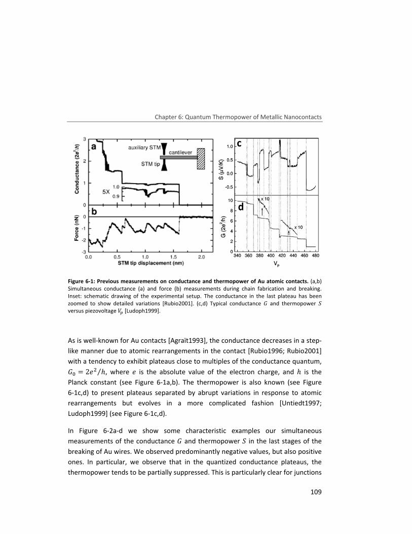
Chapter 6: Quantum Thermopower of Metallic Nanocontacts
109
Figure 6-1: Previous measurements on conductance and thermopower of Au atomic contacts. (a,b) Simultaneous conductance (a) and force (b) measurements during chain fabrication and breaking. Inset: schematic drawing of the experimental setup. The conductance in the last plateau has been zoomed to show detailed variations [Rubio2001]. (c,d) Typical conductance � and thermopower �
versus piezovoltage �� [Ludoph1999].
As is well-known for Au contacts [Agraït1993], the conductance decreases in a step-
like manner due to atomic rearrangements in the contact [Rubio1996; Rubio2001]
with a tendency to exhibit plateaus close to multiples of the conductance quantum, � = 2� ℎ⁄ , where is the absolute value of the electron charge, and ℎ is the
Planck constant (see Figure 6-1a,b). The thermopower is also known (see Figure
6-1c,d) to present plateaus separated by abrupt variations in response to atomic
rearrangements but evolves in a more complicated fashion [Untiedt1997;
Ludoph1999] (see Figure 6-1c,d).
In Figure 6-2a-d we show some characteristic examples our simultaneous
measurements of the conductance � and thermopower � in the last stages of the
breaking of Au wires. We observed predominantly negative values, but also positive
ones. In particular, we observe that in the quantized conductance plateaus, the
thermopower tends to be partially suppressed. This is particularly clear for junctions
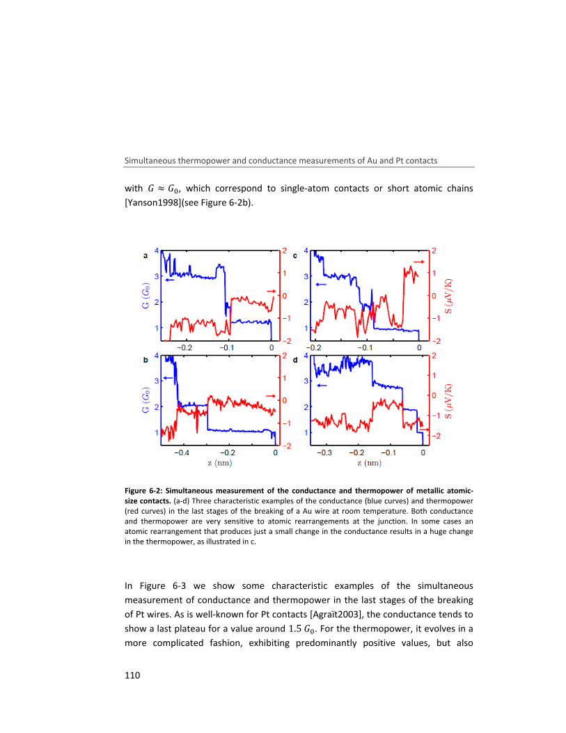
Simultaneous thermopower and conductance measurements of Au and Pt contacts
110
with � ≈ � , which correspond to single-atom contacts or short atomic chains
[Yanson1998](see Figure 6-2b).
Figure 6-2: Simultaneous measurement of the conductance and thermopower of metallic atomic-
size contacts. (a-d) Three characteristic examples of the conductance (blue curves) and thermopower (red curves) in the last stages of the breaking of a Au wire at room temperature. Both conductance and thermopower are very sensitive to atomic rearrangements at the junction. In some cases an atomic rearrangement that produces just a small change in the conductance results in a huge change in the thermopower, as illustrated in c.
In Figure 6-3 we show some characteristic examples of the simultaneous
measurement of conductance and thermopower in the last stages of the breaking
of Pt wires. As is well-known for Pt contacts [Agraıt2003], the conductance tends to
show a last plateau for a value around 1.5� . For the thermopower, it evolves in a
more complicated fashion, exhibiting predominantly positive values, but also
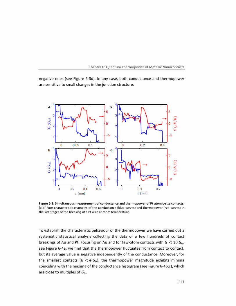
Chapter 6: Quantum Thermopower of Metallic Nanocontacts
111
negative ones (see Figure 6-3d). In any case, both conductance and thermopower
are sensitive to small changes in the junction structure.
Figure 6-3: Simultaneous measurement of conductance and thermopower of Pt atomic-size contacts. (a-d) Four characteristic examples of the conductance (blue curves) and thermopower (red curves) in the last stages of the breaking of a Pt wire at room temperature.
To establish the characteristic behaviour of the thermopower we have carried out a
systematic statistical analysis collecting the data of a few hundreds of contact
breakings of Au and Pt. Focusing on Au and for few-atom contacts with � < 10� ,
see Figure 6-4a, we find that the thermopower fluctuates from contact to contact,
but its average value is negative independently of the conductance. Moreover, for
the smallest contacts (� < 4� ), the thermopower magnitude exhibits minima
coinciding with the maxima of the conductance histogram (see Figure 6-4b,c), which
are close to multiples of � .
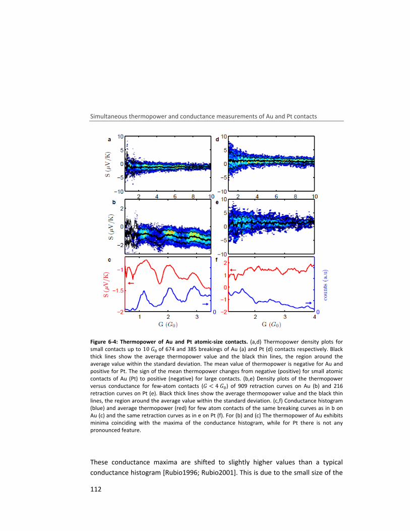
Simultaneous thermopower and conductance measurements of Au and Pt contacts
112
Figure 6-4: Thermopower of Au and Pt atomic-size contacts. (a,d) Thermopower density plots for small contacts up to 10� of 674 and 385 breakings of Au (a) and Pt (d) contacts respectively. Black thick lines show the average thermopower value and the black thin lines, the region around the average value within the standard deviation. The mean value of thermopower is negative for Au and positive for Pt. The sign of the mean thermopower changes from negative (positive) for small atomic contacts of Au (Pt) to positive (negative) for large contacts. (b,e) Density plots of the thermopower versus conductance for few-atom contacts (� < 4� ) of 909 retraction curves on Au (b) and 216 retraction curves on Pt (e). Black thick lines show the average thermopower value and the black thin lines, the region around the average value within the standard deviation. (c,f) Conductance histogram (blue) and average thermopower (red) for few atom contacts of the same breaking curves as in b on Au (c) and the same retraction curves as in e on Pt (f). For (b) and (c) The thermopower of Au exhibits minima coinciding with the maxima of the conductance histogram, while for Pt there is not any pronounced feature.
These conductance maxima are shifted to slightly higher values than a typical
conductance histogram [Rubio1996; Rubio2001]. This is due to the small size of the
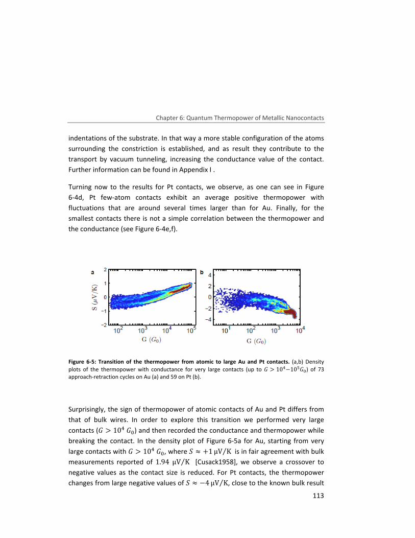
Chapter 6: Quantum Thermopower of Metallic Nanocontacts
113
indentations of the substrate. In that way a more stable configuration of the atoms
surrounding the constriction is established, and as result they contribute to the
transport by vacuum tunneling, increasing the conductance value of the contact.
Further information can be found in Appendix I .
Turning now to the results for Pt contacts, we observe, as one can see in Figure
6-4d, Pt few-atom contacts exhibit an average positive thermopower with
fluctuations that are around several times larger than for Au. Finally, for the
smallest contacts there is not a simple correlation between the thermopower and
the conductance (see Figure 6-4e,f).
Figure 6-5: Transition of the thermopower from atomic to large Au and Pt contacts. (a,b) Density plots of the thermopower with conductance for very large contacts (up to � > 10Ó−10Ò� ) of 73 approach-retraction cycles on Au (a) and 59 on Pt (b).
Surprisingly, the sign of thermopower of atomic contacts of Au and Pt differs from
that of bulk wires. In order to explore this transition we performed very large
contacts (� > 10Ó� ) and then recorded the conductance and thermopower while
breaking the contact. In the density plot of Figure 6-5a for Au, starting from very
large contacts with � > 10Ó� , where � ≈ +1μV K⁄ is in fair agreement with bulk
measurements reported of 1.94 μV K⁄ [Cusack1958], we observe a crossover to
negative values as the contact size is reduced. For Pt contacts, the thermopower
changes from large negative values of � ≈ −4μV K⁄ , close to the known bulk result
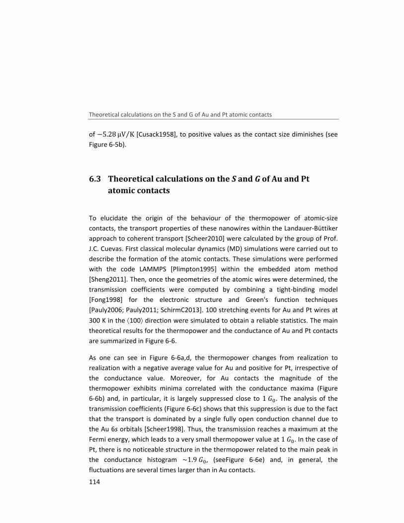
Theoretical calculations on the S and G of Au and Pt atomic contacts
114
of −5.28 μV K⁄ [Cusack1958], to positive values as the contact size diminishes (see
Figure 6-5b).
6.3 Theoretical calculations on the S and G of Au and Pt
atomic contacts
To elucidate the origin of the behaviour of the thermopower of atomic-size
contacts, the transport properties of these nanowires within the Landauer-Büttiker
approach to coherent transport [Scheer2010] were calculated by the group of Prof.
J.C. Cuevas. First classical molecular dynamics (MD) simulations were carried out to
describe the formation of the atomic contacts. These simulations were performed
with the code LAMMPS [Plimpton1995] within the embedded atom method
[Sheng2011]. Then, once the geometries of the atomic wires were determined, the
transmission coefficients were computed by combining a tight-binding model
[Fong1998] for the electronic structure and Green's function techniques
[Pauly2006; Pauly2011; SchirmC2013]. 100 stretching events for Au and Pt wires at
300 K in the ⟨100⟩ direction were simulated to obtain a reliable statistics. The main
theoretical results for the thermopower and the conductance of Au and Pt contacts
are summarized in Figure 6-6.
As one can see in Figure 6-6a,d, the thermopower changes from realization to
realization with a negative average value for Au and positive for Pt, irrespective of
the conductance value. Moreover, for Au contacts the magnitude of the
thermopower exhibits minima correlated with the conductance maxima (Figure
6-6b) and, in particular, it is largely suppressed close to 1� . The analysis of the
transmission coefficients (Figure 6-6c) shows that this suppression is due to the fact
that the transport is dominated by a single fully open conduction channel due to
the Au 6s orbitals [Scheer1998]. Thus, the transmission reaches a maximum at the
Fermi energy, which leads to a very small thermopower value at 1� . In the case of
Pt, there is no noticeable structure in the thermopower related to the main peak in
the conductance histogram ~1.9� , (seeFigure 6-6e) and, in general, the
fluctuations are several times larger than in Au contacts.
Chapter 6: Quantum Thermopower of Metallic Nanocontacts
115
Figure 6-6: Computed thermopower and conductance of Au and Pt atomic contacts. (by Prof. J.C. Cuevas’ group). (a) Density plot of the thermopower as a function of the conductance computed from 100 simulations of the stretching of Au contacts at room temperature. The solid black line indicates the average value, while the dashed lines delimit the region around the average value within the standard deviation. Notice that the average value of S is negative. (b) The corresponding computed conductance histogram for Au contacts. The most salient feature is the appearance of a peak close to 1� . (c) The 10 largest transmission coefficients as a function of the conductance. The lines correspond to the average values and the bars to the standard deviations. Notice that the region close to 1� is dominated by a single fully open channel. (d-f) The same as in panels a-c but for Pt. Notice that the average thermopower is positive. The conductance histograms exhibits a peak at around 1.9� , which corresponds to single-atom contacts and short atomic chains. This conductance region is dominated by 4 conductions channels.
We attribute these features to the fact that the transport in Pt contacts is
dominated by the 5d orbitals [Pauly2006]. This implies that several partially open
channels contribute to the transport even in single-atom contacts, see Figure 6-6f.
Thus, the transmission does not reach an extremum at the Fermi energy and the
Theoretical calculations on the S and G of Au and Pt atomic contacts
116
thermopower is not suppressed. Moreover, the d orbitals are anisotropic and thus
much more sensitive to local disorder than the Y orbitals, which leads to larger
fluctuations in the thermopower for Pt [Pauly2011]. Overall, these results are in
very good qualitative agreement with our experimental findings.
Let us now discuss about the origin of the sign of the thermopower. In Figure 6-7a,c
we show the total transmission as a function of energy for Au and Pt few-atom
contacts obtained along the same stretching simulation. Notice that while the slope
around the Fermi energy, +8, is typically positive for the Au contacts, leading to a
negative thermopower, it is mainly negative in the case of Pt, which results in a
positive thermopower. This different behaviour can be traced back to the different
electronic structures of these two metals. In the case of Au, +8 lies on a region
dominated by the 6s orbitals with smaller contributions from the 6p bands. The
density of states (DOS) for these orbitals, which are responsible for the transport,
tends to slightly increase with energy. This is illustrated in Figure 6-7b where we
show the local DOS projected onto the different orbitals of a central atom in a two-
atom contact. Contrary, for Pt +8 lies close to the edge of the 5d bands, a region
where the transmission typically diminishes with increasing energy. This reflects in
turn the typical behaviour of the local DOS, as we show in Figure 6-7d for a single-
atom contact.
It is worth comparing with previous results. For Au our results are in qualitative
agreement with those recently reported in ref [Tsutsui2013], while the
interpretation is clearly at variance. To explain their results, invoked simple free-
electron models meant to describe ballistic quantum point contacts. However,
these models only predict a negative sign for the thermopower and they are thus
unable to explain the appearance of positive values in some Au contacts or the
typical behavior of the Pt contacts. This shows that our results cannot be simply
explained in terms of quantum confinement. On the other hand, the claim in ref
[Ludoph1999] that the thermopower of Au contacts vanishes on average is due to
the fact that those experiments were performed at a much lower temperature (12
K) and thus, the thermopower is expected to be around 30 times smaller than in our
case [Pauly2011]. Moreover, the role of the impurities advocated in that work to
explain the behavior of the thermopower fluctuations is certainly important, but in
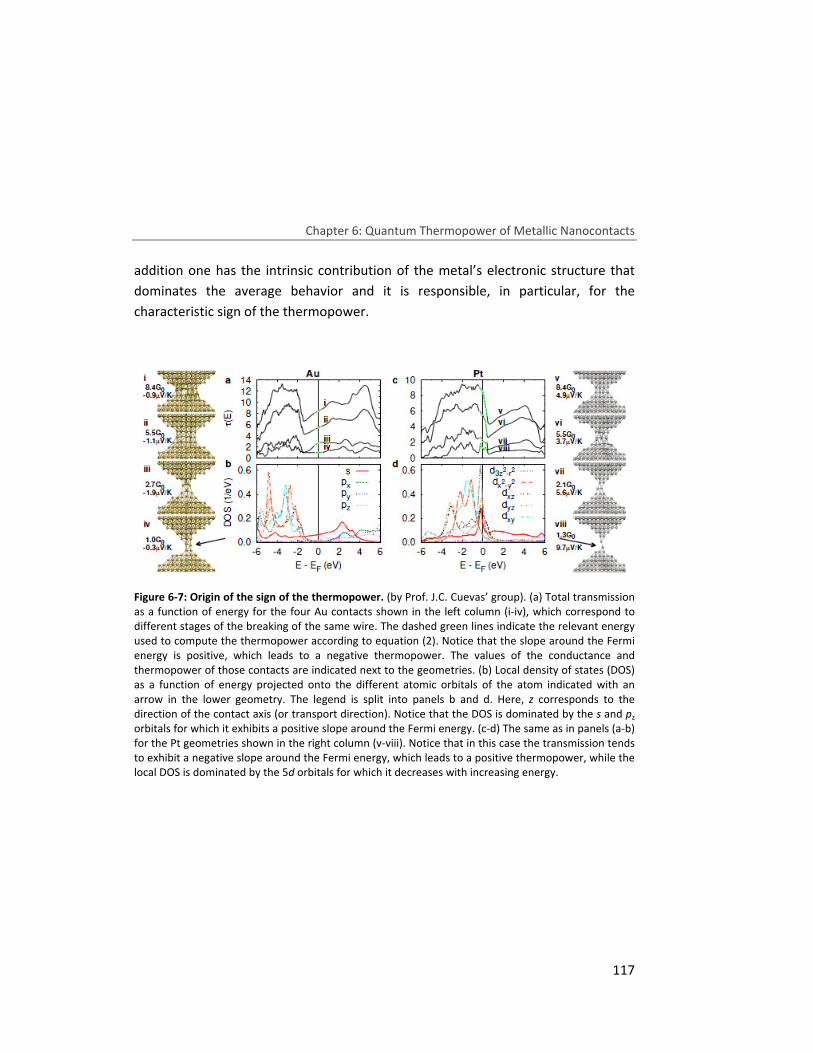
Chapter 6: Quantum Thermopower of Metallic Nanocontacts
117
addition one has the intrinsic contribution of the metal’s electronic structure that
dominates the average behavior and it is responsible, in particular, for the
characteristic sign of the thermopower.
Figure 6-7: Origin of the sign of the thermopower. (by Prof. J.C. Cuevas’ group). (a) Total transmission as a function of energy for the four Au contacts shown in the left column (i-iv), which correspond to different stages of the breaking of the same wire. The dashed green lines indicate the relevant energy used to compute the thermopower according to equation (2). Notice that the slope around the Fermi energy is positive, which leads to a negative thermopower. The values of the conductance and thermopower of those contacts are indicated next to the geometries. (b) Local density of states (DOS) as a function of energy projected onto the different atomic orbitals of the atom indicated with an arrow in the lower geometry. The legend is split into panels b and d. Here, z corresponds to the direction of the contact axis (or transport direction). Notice that the DOS is dominated by the s and pz orbitals for which it exhibits a positive slope around the Fermi energy. (c-d) The same as in panels (a-b) for the Pt geometries shown in the right column (v-viii). Notice that in this case the transmission tends to exhibit a negative slope around the Fermi energy, which leads to a positive thermopower, while the local DOS is dominated by the 5d orbitals for which it decreases with increasing energy.
Conclusions
118
6.4 Conclusions
In this chapter, we investigated the thermopower of Au and Pt metallic contacts in
the nanoscale. This system offers the unique possibility of investigating how
thermoelectricity is continuously modified from bulk all the way down to the atomic
scale where quantum effects dominate. We found that the thermopower, changes
not only its magnitude but also its sign when the contact size dimensions are
reduced to the size of a single atom. Moreover, we find that in the case of gold, the
thermopower of a few-atom contact exhibits a series of minima correlated with the
maxima of the conductance, in marked contrast with the platinum wires where
such oscillations are absent. Coherent transport theoretical calculations by Prof. J.C.
Cuevas’ group, demonstrate that the different behaviour of the two metals can be
explained in terms of their different electronic structure.
Chapter 6: Quantum Thermopower of Metallic Nanocontacts
119
References
[Agraït1993] Agraït, N., J. G. Rodrigo and S. Vieira (1993). "Conductance steps and
quantization in atomic-size contacts." Physical Review B 47(18): 12345-12348.
[Agraït1995] Agraït, N., G. Rubio and S. Vieira (1995). "Plastic Deformation of Nanometer-Scale Gold Connective Necks." Physical Review Letters 74(20): 3995-3998.
[Agraıt2003] Agraıt, N., A. L. Yeyati and J. M. van Ruitenbeek (2003). "Quantum properties of atomic-sized conductors." Physics Reports 377(2–3): 81-279.
[Blatt1976] Blatt, F. J. (1976). Thermoelectric Power of Metals, Plenum Press. [Cusack1958] Cusack, N. and P. Kendall (1958). "The Absolute Scale of
Thermoelectric Power at High Temperature." Proceedings of the Physical Society (1960) 72(5): 898-901.
[Fong1998] Fong, C. (1998). Topics in Computational Materials Science, World Scientific.
[Ludoph1999] Ludoph, B. and J. M. v. Ruitenbeek (1999). "Thermopower of atomic-size metallic contacts." Physical Review B 59(19): 12290-12293.
[Mott1936] Mott, N. F. and H. Jones (1936). The Theory of the Properties of Metals and Alloys, Clarendon Press.
[Pauly2006] Pauly, F., M. Dreher, J. K. Viljas, M. Häfner, J. C. Cuevas, et al. (2006). "Theoretical analysis of the conductance histograms and structural properties of Ag, Pt, and Ni nanocontacts." Physical Review B 74(23): 235106.
[Pauly2011] Pauly, F., J. K. Viljas, M. Bürkle, M. Dreher, P. Nielaba, et al. (2011). "Molecular dynamics study of the thermopower of Ag, Au, and Pt nanocontacts." Physical Review B 84(19): 195420.
[Plimpton1995] Plimpton, S. (1995). "Fast Parallel Algorithms for Short-Range Molecular Dynamics." Journal of Computational Physics 117(1): 1-19.
[Rubio1996] Rubio, G., N. Agraït and S. Vieira (1996). "Atomic-Sized Metallic Contacts: Mechanical Properties and Electronic Transport." Physical Review Letters 76(13): 2302-2305.
[Rubio2001] Rubio, G., S. R. Bahn, N. Agraït, K. W. Jacobsen and S. Vieira (2001). "Mechanical Properties and Formation Mechanisms of a Wire of Single Gold Atoms." Physical Review Letters 87(2): 026101.
[Scheer2010] Scheer, E. (2010). Molecular Electronics: An Introduction to Theory and Experiment, World Scientific Publishing Company Pte Limited.
References
120
[Scheer1998] Scheer, E., N. Agrait, J. C. Cuevas, A. L. Yeyati, B. Ludoph, et al. (1998). "The signature of chemical valence in the electrical conduction through a single-atom contact." Nature 394(6689): 154-157.
[SchirmC2013] SchirmC, MattM, PaulyF, J. C. Cuevas, NielabaP, et al. (2013). "A current-driven single-atom memory." Nat Nano 8(9): 645-648.
[Sheng2011] Sheng, H. W., M. J. Kramer, A. Cadien, T. Fujita and M. W. Chen (2011). "Highly optimized embedded-atom-method potentials for fourteen fcc metals." Physical Review B 83(13): 134118.
[Tsutsui2013] Tsutsui, M., T. Morikawa, A. Arima and M. Taniguchi (2013). "Thermoelectricity in atom-sized junctions at room temperatures." Sci. Rep. 3.
[Untiedt1997] Untiedt, C., G. Rubio, S. Vieira and N. Agraït (1997). "Fabrication and characterization of metallic nanowires." Physical Review B 56(4): 2154-2160.
[Yanson1998] Yanson, A. I., G. R. Bollinger, H. E. van den Brom, N. Agrait and J. M. van Ruitenbeek (1998). "Formation and manipulation of a metallic wire of single gold atoms." Nature 395(6704): 783-785.
In this chapter we explore how
modification
electron
also study the evolution of thermopower during stretching of the molecular
junction
7.1
In chapter
junctions can be enha
molecules.
to now
function of metallic electrodes
single
and varying the chemical composition
also been
if the transmission spectrum contains a Fano resonance close to the Fermi level
[Bergfield2009
have
In this chapter we explore how
modification of the molecular level
electron-rich groups to the
also study the evolution of thermopower during stretching of the molecular
junction.
7.1 Introduction
In chapter 5 we have demonstrated that the thermopower
junctions can be enha
molecules. Improving
now, by varying the position of intramolecular energy levels relative to the work
function of metallic electrodes
single-molecule lengths within a family of molecules
and varying the chemical composition
also been predicted that extremely high
if the transmission spectrum contains a Fano resonance close to the Fermi level
Bergfield2009;
have not been demonstrated experimentally.
Chapter
In this chapter we explore how
of the molecular level
ch groups to the Oligo
also study the evolution of thermopower during stretching of the molecular
Introduction
we have demonstrated that the thermopower
junctions can be enhanced by tuning the intermolecular coupling between
Improving � in molecular junctions has been shown in several ways up
varying the position of intramolecular energy levels relative to the work
function of metallic electrodes
molecule lengths within a family of molecules
and varying the chemical composition
predicted that extremely high
if the transmission spectrum contains a Fano resonance close to the Fermi level
; Finch2009; Bergfield2010
been demonstrated experimentally.
Chapter 7: Enhancing the Thermopower of OPE Molecular Junctions
In this chapter we explore how thermopower maybe enhance by
of the molecular level. In particular
Oligophenylene
also study the evolution of thermopower during stretching of the molecular
we have demonstrated that the thermopower
nced by tuning the intermolecular coupling between
in molecular junctions has been shown in several ways up
varying the position of intramolecular energy levels relative to the work
function of metallic electrodes [Yee2010
molecule lengths within a family of molecules
and varying the chemical composition [Baheti2008
predicted that extremely high figure of merit,
if the transmission spectrum contains a Fano resonance close to the Fermi level
Bergfield2010
been demonstrated experimentally.
Enhancing the Thermopower of OPE Molecular Junctions
thermopower maybe enhance by
. In particular, we investigate
phenylene ethylene (OPE
also study the evolution of thermopower during stretching of the molecular
we have demonstrated that the thermopower
nced by tuning the intermolecular coupling between
in molecular junctions has been shown in several ways up
varying the position of intramolecular energy levels relative to the work
Yee2010; Yee2011],
molecule lengths within a family of molecules
Baheti2008]. For mole
figure of merit,
if the transmission spectrum contains a Fano resonance close to the Fermi level
Bergfield2010]. As far as we know, however, examples
been demonstrated experimentally.
Enhancing the Thermopower of OPE Molecular Junctions
thermopower maybe enhance by
we investigate
(OPE) molecular backbone
also study the evolution of thermopower during stretching of the molecular
we have demonstrated that the thermopower (
nced by tuning the intermolecular coupling between
in molecular junctions has been shown in several ways up
varying the position of intramolecular energy levels relative to the work
, systematically increasing the
[Malen2009;
For molecular junctions, it has
figure of merit, �, values can be reached
if the transmission spectrum contains a Fano resonance close to the Fermi level
. As far as we know, however, examples
Enhancing the Thermopower of OPE Molecular Junctions
thermopower maybe enhance by structural
we investigate the addition of
lar backbone.
also study the evolution of thermopower during stretching of the molecular
(�) of molecular
nced by tuning the intermolecular coupling between
in molecular junctions has been shown in several ways up
varying the position of intramolecular energy levels relative to the work
systematically increasing the
; Widawsky2013
cular junctions, it has
values can be reached
if the transmission spectrum contains a Fano resonance close to the Fermi level
. As far as we know, however, examples
Enhancing the Thermopower of OPE Molecular Junctions
121
structural
the addition of
. We
also study the evolution of thermopower during stretching of the molecular
of molecular
nced by tuning the intermolecular coupling between C60
in molecular junctions has been shown in several ways up
varying the position of intramolecular energy levels relative to the work
systematically increasing the
Widawsky2013]
cular junctions, it has
values can be reached
if the transmission spectrum contains a Fano resonance close to the Fermi level
. As far as we know, however, examples
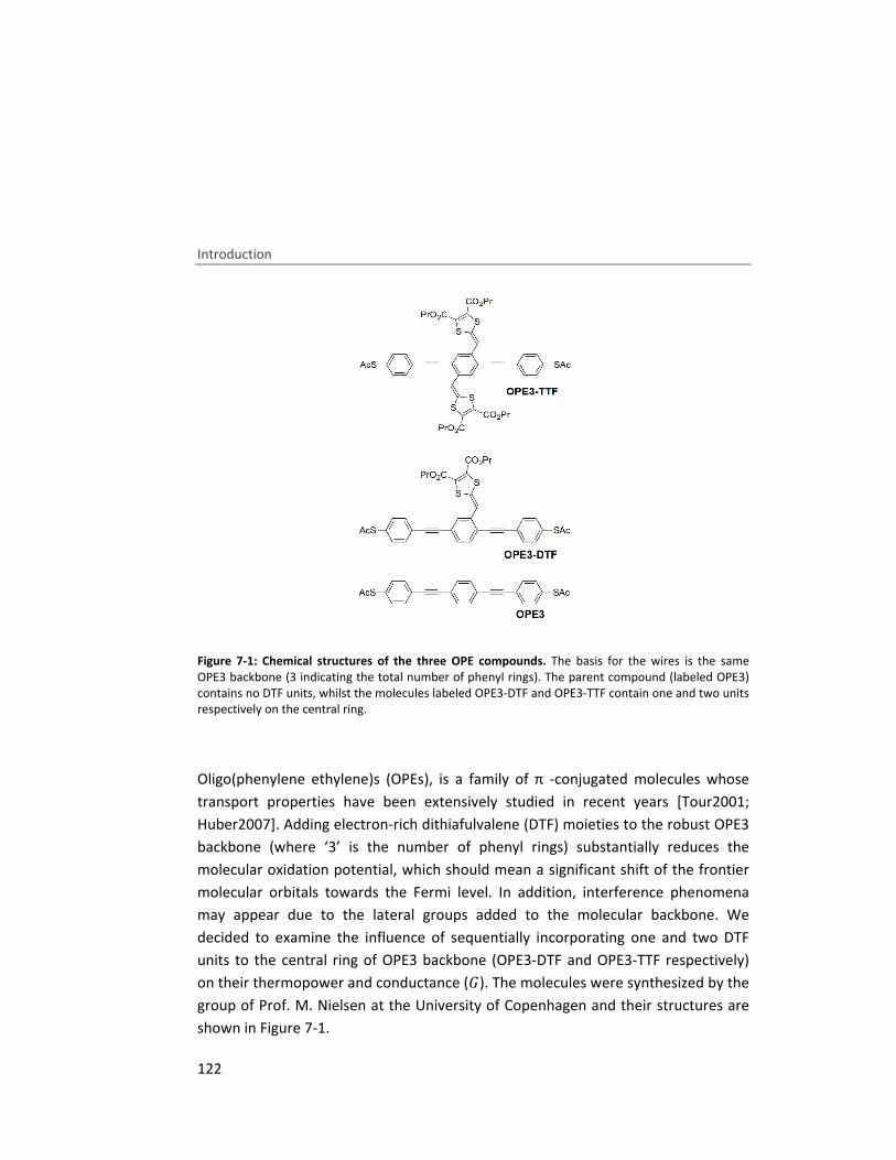
Introduction
122
Figure 7-1: Chemical structures of the three OPE compounds. The basis for the wires is the same OPE3 backbone (3 indicating the total number of phenyl rings). The parent compound (labeled OPE3) contains no DTF units, whilst the molecules labeled OPE3-DTF and OPE3-TTF contain one and two units respectively on the central ring.
Oligo(phenylene ethylene)s (OPEs), is a family of π -conjugated molecules whose
transport properties have been extensively studied in recent years [Tour2001;
Huber2007]. Adding electron-rich dithiafulvalene (DTF) moieties to the robust OPE3
backbone (where ‘3’ is the number of phenyl rings) substantially reduces the
molecular oxidation potential, which should mean a significant shift of the frontier
molecular orbitals towards the Fermi level. In addition, interference phenomena
may appear due to the lateral groups added to the molecular backbone. We
decided to examine the influence of sequentially incorporating one and two DTF
units to the central ring of OPE3 backbone (OPE3-DTF and OPE3-TTF respectively)
on their thermopower and conductance (�). The molecules were synthesized by the
group of Prof. M. Nielsen at the University of Copenhagen and their structures are
shown in Figure 7-1.
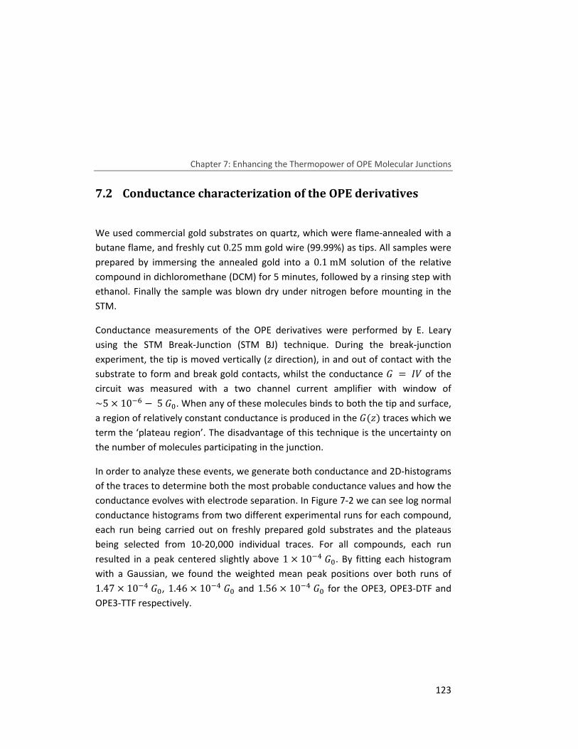
Chapter 7: Enhancing the Thermopower of OPE Molecular Junctions
123
7.2 Conductance characterization of the OPE derivatives
We used commercial gold substrates on quartz, which were flame-annealed with a
butane flame, and freshly cut 0.25mm gold wire (99.99%) as tips. All samples were
prepared by immersing the annealed gold into a 0.1mM solution of the relative
compound in dichloromethane (DCM) for 5 minutes, followed by a rinsing step with
ethanol. Finally the sample was blown dry under nitrogen before mounting in the
STM.
Conductance measurements of the OPE derivatives were performed by E. Leary
using the STM Break-Junction (STM BJ) technique. During the break-junction
experiment, the tip is moved vertically (¿ direction), in and out of contact with the
substrate to form and break gold contacts, whilst the conductance � = � of the
circuit was measured with a two channel current amplifier with window of
~5 × 10�Î − 5� . When any of these molecules binds to both the tip and surface,
a region of relatively constant conductance is produced in the �(¿) traces which we
term the ‘plateau region’. The disadvantage of this technique is the uncertainty on
the number of molecules participating in the junction.
In order to analyze these events, we generate both conductance and 2D-histograms
of the traces to determine both the most probable conductance values and how the
conductance evolves with electrode separation. In Figure 7-2 we can see log normal
conductance histograms from two different experimental runs for each compound,
each run being carried out on freshly prepared gold substrates and the plateaus
being selected from 10-20,000 individual traces. For all compounds, each run
resulted in a peak centered slightly above 1 × 10�Ó� . By fitting each histogram
with a Gaussian, we found the weighted mean peak positions over both runs of
1.47 × 10�Ó� , 1.46 × 10�Ó� and 1.56 × 10�Ó� for the OPE3, OPE3-DTF and
OPE3-TTF respectively.
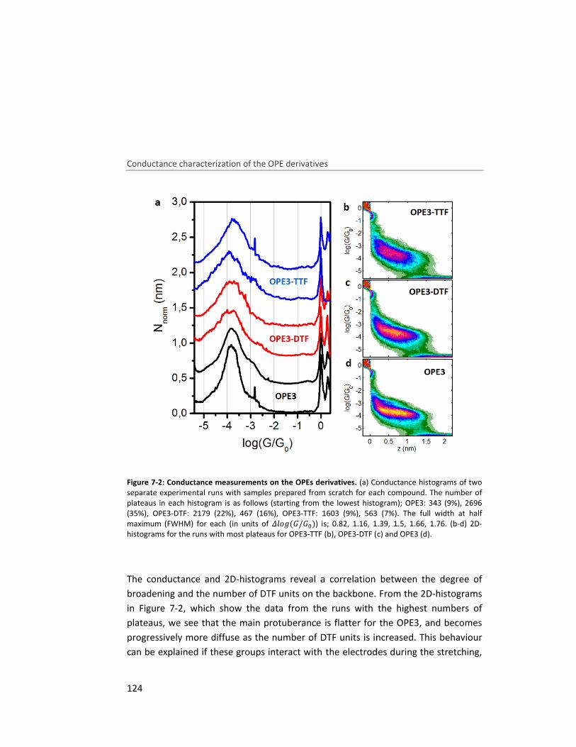
Conductance characterization of the OPE derivatives
124
Figure 7-2
separate experimental runs with samples prepared from scratch for each coplateaus in each histogram is as follows (starting from the lowest histogram); OPE3: 343 (9%), 2696 (35%), OPE3maximum (FWHM) for each (in units of histograms for the runs with m
The conductance
broadening
in Figure
plateaus, we see that the main protuberance is flatter for the OPE3, and become
progressively more diffuse as the number of DTF units is increased. This
can be explained if these groups interact with the electrodes during the stretching,
Conductance characterization of the OPE derivatives
2: Conductance measurements
separate experimental runs with samples prepared from scratch for each coplateaus in each histogram is as follows (starting from the lowest histogram); OPE3: 343 (9%), 2696 (35%), OPE3-DTF: 2179 (22%), 467 (16%), OPE3maximum (FWHM) for each (in units of histograms for the runs with m
conductance and 2D
broadening and the nu
Figure 7-2, which show the data from the runs with the highest numbers of
plateaus, we see that the main protuberance is flatter for the OPE3, and become
progressively more diffuse as the number of DTF units is increased. This
can be explained if these groups interact with the electrodes during the stretching,
Conductance characterization of the OPE derivatives
: Conductance measurements
separate experimental runs with samples prepared from scratch for each coplateaus in each histogram is as follows (starting from the lowest histogram); OPE3: 343 (9%), 2696
DTF: 2179 (22%), 467 (16%), OPE3maximum (FWHM) for each (in units of histograms for the runs with most plateaus for OPE3
and 2D-histograms reveal a correlation b
and the number of DTF uni
, which show the data from the runs with the highest numbers of
plateaus, we see that the main protuberance is flatter for the OPE3, and become
progressively more diffuse as the number of DTF units is increased. This
can be explained if these groups interact with the electrodes during the stretching,
Conductance characterization of the OPE derivatives
on the OPEs derivatives
separate experimental runs with samples prepared from scratch for each coplateaus in each histogram is as follows (starting from the lowest histogram); OPE3: 343 (9%), 2696
DTF: 2179 (22%), 467 (16%), OPE3-TTF: 1603 (9%), 563 (7%). The full width at half maximum (FWHM) for each (in units of � Wz(�/� �) is; 0.82, 1.16, 1.39, 1.5, 1.66, 1.76.
ost plateaus for OPE3-TTF (b), OPE3
histograms reveal a correlation b
mber of DTF units on the backbone. From the 2D
, which show the data from the runs with the highest numbers of
plateaus, we see that the main protuberance is flatter for the OPE3, and become
progressively more diffuse as the number of DTF units is increased. This
can be explained if these groups interact with the electrodes during the stretching,
Conductance characterization of the OPE derivatives
on the OPEs derivatives. (a) Conductanceseparate experimental runs with samples prepared from scratch for each coplateaus in each histogram is as follows (starting from the lowest histogram); OPE3: 343 (9%), 2696
TTF: 1603 (9%), 563 (7%). The full width at half ) is; 0.82, 1.16, 1.39, 1.5, 1.66, 1.76.
TTF (b), OPE3-DTF (c) and OPE3 (d).
histograms reveal a correlation b
ts on the backbone. From the 2D
, which show the data from the runs with the highest numbers of
plateaus, we see that the main protuberance is flatter for the OPE3, and become
progressively more diffuse as the number of DTF units is increased. This
can be explained if these groups interact with the electrodes during the stretching,
Conductance histograms of two separate experimental runs with samples prepared from scratch for each compound. The number of plateaus in each histogram is as follows (starting from the lowest histogram); OPE3: 343 (9%), 2696
TTF: 1603 (9%), 563 (7%). The full width at half ) is; 0.82, 1.16, 1.39, 1.5, 1.66, 1.76.
DTF (c) and OPE3 (d).
histograms reveal a correlation between the degree of
ts on the backbone. From the 2D
, which show the data from the runs with the highest numbers of
plateaus, we see that the main protuberance is flatter for the OPE3, and become
progressively more diffuse as the number of DTF units is increased. This
can be explained if these groups interact with the electrodes during the stretching,
histograms of two mpound. The number of
plateaus in each histogram is as follows (starting from the lowest histogram); OPE3: 343 (9%), 2696 TTF: 1603 (9%), 563 (7%). The full width at half
) is; 0.82, 1.16, 1.39, 1.5, 1.66, 1.76. (b-d) 2D-DTF (c) and OPE3 (d).
etween the degree of
ts on the backbone. From the 2D-histograms
, which show the data from the runs with the highest numbers of
plateaus, we see that the main protuberance is flatter for the OPE3, and becomes
progressively more diffuse as the number of DTF units is increased. This behaviour
can be explained if these groups interact with the electrodes during the stretching,
Chapter 7: Enhancing the Thermopower of OPE Molecular Junctions
125
which would cause the molecule to fluctuate more during stretching, and may also
provide additional conductance pathways through the molecule.
7.3 Simultaneous thermopower and conductance
measurements of the OPE derivatives
We measured the thermopower by implementing the technique described in
chapter 4 in the STM BJ technique. During retraction we stop the tip motion every 50pm and we ramp the voltage between ±7mV. The bias voltage is set at
���� = 50mV. The range of the conductance monitored is limited between
1 × 10�Ò − 2 × 10�N� , because for the thermopower measurements we use a
one channel current amplifier in order to minimize the electronical offsets. (see
chapter 4). Measurements were repeated for various tip-sample temperature
gradients (��), all around 20K and 40K.
In Figure 7-3 we show some characteristic examples of simultaneous � and �
measurements during the stretching for OPE3, OPE3-DTF and OPE3-TTF molecular
junctions. When a molecule binds to both the tip and the surface, the conductance,
�(¿) (blue traces), and thermopower, �(¿)(red traces), remain relatively constant
forming plateaus whose mean thermopower value varies from junction to junction.
The largest values of the mean thermopower for individual plateaus can be as high
as 25μV K⁄ (curve 2 Figure 7-3c) for OPE3-TTF, 22 μV K⁄ for an OPE-DTF (curve 3
Figure 7-3b) and slightly less up to 18μV K⁄ for the OPE3 (curve 3 Figure 7-3a). We
also found plateaus with very low thermopower around 2-3μV K⁄ (curve 1 Figure
7-3a and curve 4 Figure 7-3b).
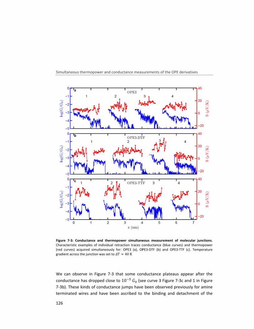
Simultaneous thermopower and conductance measurements of the OPE derivatives
126
Figure 7-3
Characteristic examples of individual retraction(red curves) acquired simultaneously for: OPE3gradient across the junction was set to
We can observe in
conductance has
7-3b). These
terminated wires
multaneous thermopower and conductance measurements of the OPE derivatives
3: Conductance and thermopower simultaneous measurement of
Characteristic examples of individual retraction(red curves) acquired simultaneously for: OPE3gradient across the junction was set to
We can observe in Figure
conductance has dropped
). These kinds of conductance jumps have been observed previously for
terminated wires and
multaneous thermopower and conductance measurements of the OPE derivatives
: Conductance and thermopower simultaneous measurement of
Characteristic examples of individual retraction(red curves) acquired simultaneously for: OPE3gradient across the junction was set to ��
Figure 7-3 that s
dropped close to
of conductance jumps have been observed previously for
and have been
multaneous thermopower and conductance measurements of the OPE derivatives
: Conductance and thermopower simultaneous measurement of
Characteristic examples of individual retraction traces conductance (blue curves) and thermopower (red curves) acquired simultaneously for: OPE3 (a), OPE3�� ≈ 40K
that some conductance plateaus appe
close to 10�Ò� (see curve 3
of conductance jumps have been observed previously for
been ascribed to the binding and deta
multaneous thermopower and conductance measurements of the OPE derivatives
: Conductance and thermopower simultaneous measurement of
traces conductance (blue curves) and thermopower , OPE3-DTF (b) and OPE3
onductance plateaus appe
(see curve 3 Figure
of conductance jumps have been observed previously for
ascribed to the binding and deta
multaneous thermopower and conductance measurements of the OPE derivatives
: Conductance and thermopower simultaneous measurement of molecular junctions.
traces conductance (blue curves) and thermopower and OPE3-TTF (c). Temperature
onductance plateaus appear after the
Figure 7-3c and 1 in
of conductance jumps have been observed previously for
ascribed to the binding and detachment of the
multaneous thermopower and conductance measurements of the OPE derivatives
molecular junctions. traces conductance (blue curves) and thermopower
. Temperature
ar after the
and 1 in Figure
of conductance jumps have been observed previously for amine
chment of the

Chapter 7: Enhancing the Thermopower of OPE Molecular Junctions
127
molecules during break-junction experiments [González2013]. This conclusion can
be confirmed here by the switching of thermopower from zero to a plateau for the
corresponding jump in conductance.
We generated the 2D-histograms for the �(¿) and �(�)out of the data acquired
from the − �s for the three molecules in order to see how the thermopower
evolves with the electrode separation and with conductance (see Figure 7-4). �(¿) 2D-histograms are also plotted. From the 2D-histograms for the �(¿)(Figure 7-4d-f)
we see a high dispersion of the thermopower for all molecules. This is due to the
fluctuations on individual plateaus and the variation from plateau to plateau of the
average thermopower. The dispersion of thermopower increases with the number
of DTF units. Conductance, on the other hand, has higher dispersion, varying more
than one order of magnitude (see 2D-histograms �(�) in Figure 7-4g-i) indicating
the higher sensitivity of � than � to atomic-scale fluctuations.
For all the molecules we also see that thermopower generally increases (up to 25%)
while stretching the molecular junction (see Figure 7-4d-f) and finally stabilizes at
the end of the plateau. This sensitivity to stretching, which is more pronounced in
the OPE3-TTF molecule (see Figure 7-4f), is possibly due to shifting and narrowing of
the energy levels since the coupling of the molecule to the metallic electrodes is
changing by stretching the junction. This effect has not been previously reported.
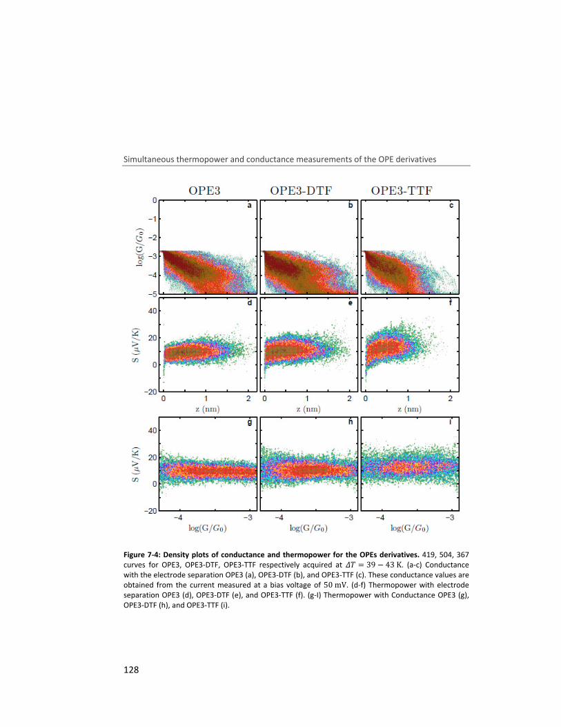
Simultaneous thermopower and conductance measurements of the OPE derivatives
128
Figure 7-4: Density plots of conductance and thermopower for the OPEs derivatives. 419, 504, 367 curves for OPE3, OPE3-DTF, OPE3-TTF respectively acquired at �� = 39 − 43K. (a-c) Conductance with the electrode separation OPE3 (a), OPE3-DTF (b), and OPE3-TTF (c). These conductance values are obtained from the current measured at a bias voltage of 50mV. (d-f) Thermopower with electrode separation OPE3 (d), OPE3-DTF (e), and OPE3-TTF (f). (g-I) Thermopower with Conductance OPE3 (g), OPE3-DTF (h), and OPE3-TTF (i).
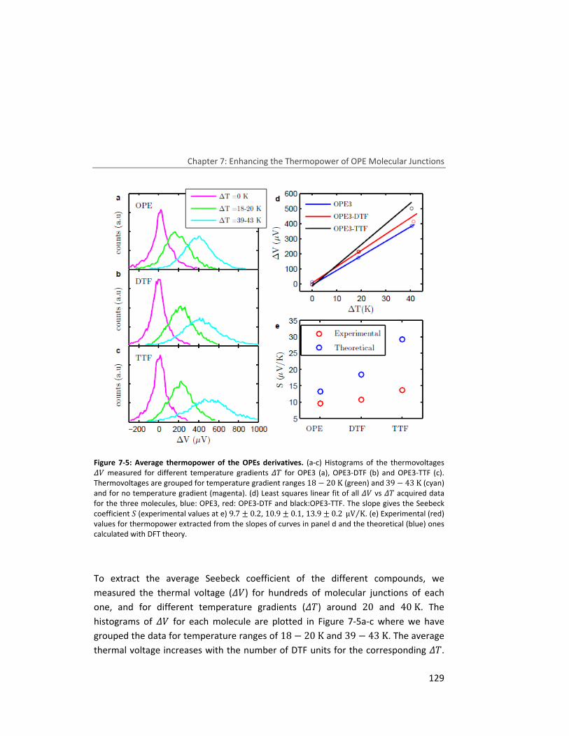
Chapter 7: Enhancing the Thermopower of OPE Molecular Junctions
129
Figure 7-5: Average thermopower of the OPEs derivatives. (a-c) Histograms of the thermovoltages �� measured for different temperature gradients �� for OPE3 (a), OPE3-DTF (b) and OPE3-TTF (c). Thermovoltages are grouped for temperature gradient ranges 18 − 20K (green) and39 − 43K (cyan) and for no temperature gradient (magenta). (d) Least squares linear fit of all �� vs �� acquired data for the three molecules, blue: OPE3, red: OPE3-DTF and black:OPE3-TTF. The slope gives the Seebeck coefficient �(experimental values at e) 9.7 Ä 0.2, 10.9 Ä 0.1, 13.9 Ä 0.2 μV K⁄ . (e) Experimental (red) values for thermopower extracted from the slopes of curves in panel d and the theoretical (blue) ones calculated with DFT theory.
To extract the average Seebeck coefficient of the different compounds, we
measured the thermal voltage (��) for hundreds of molecular junctions of each
one, and for different temperature gradients (��) around 20 and 40K. The
histograms of �� for each molecule are plotted in Figure 7-5a-c where we have
grouped the data for temperature ranges of 18 − 20K and 39 − 43K. The average
thermal voltage increases with the number of DTF units for the corresponding ��.
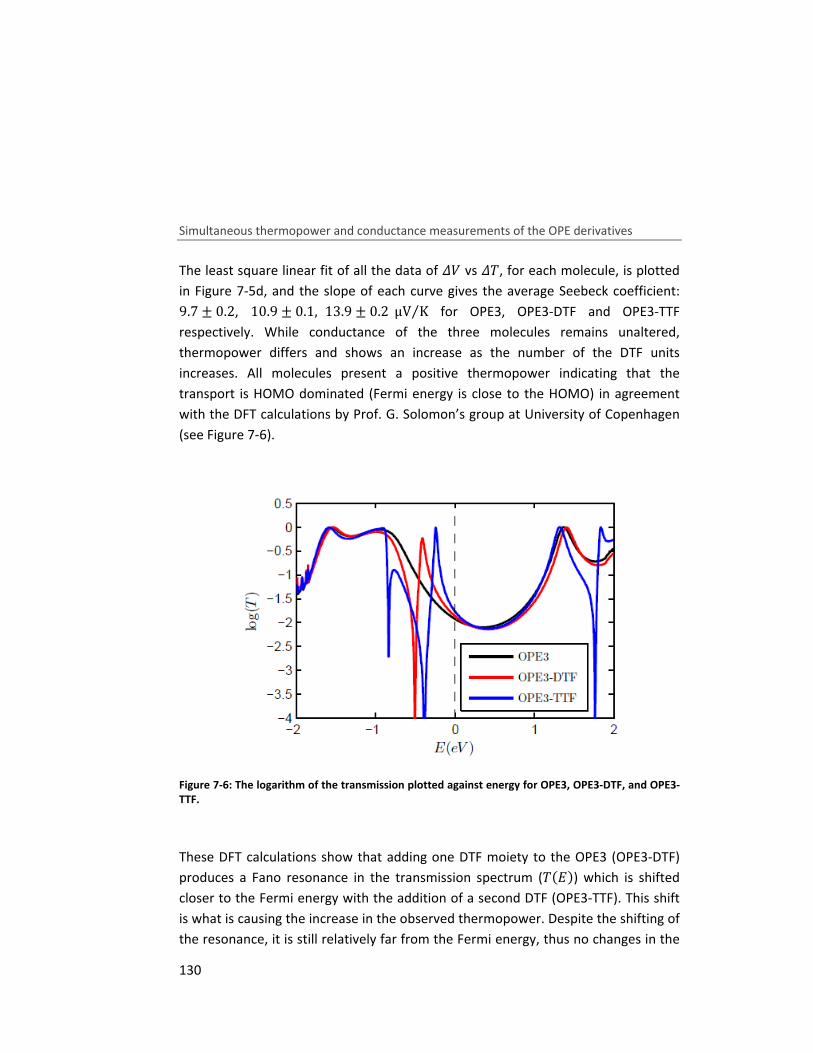
Simultaneous thermopower and conductance measurements of the OPE derivatives
130
The least square linear fit of all the data of �� vs ��, for each molecule, is plotted
in Figure 7-5d, and the slope of each curve gives the average Seebeck coefficient: 9.7 Ä 0.2, 10.9 Ä 0.1, 13.9 Ä 0.2 μV K⁄ for OPE3, OPE3-DTF and OPE3-TTF
respectively. While conductance of the three molecules remains unaltered,
thermopower differs and shows an increase as the number of the DTF units
increases. All molecules present a positive thermopower indicating that the
transport is HOMO dominated (Fermi energy is close to the HOMO) in agreement
with the DFT calculations by Prof. G. Solomon’s group at University of Copenhagen
(see Figure 7-6).
Figure 7-6: The logarithm of the transmission plotted against energy for OPE3, OPE3-DTF, and OPE3-
TTF.
These DFT calculations show that adding one DTF moiety to the OPE3 (OPE3-DTF)
produces a Fano resonance in the transmission spectrum (�(+)) which is shifted
closer to the Fermi energy with the addition of a second DTF (OPE3-TTF). This shift
is what is causing the increase in the observed thermopower. Despite the shifting of
the resonance, it is still relatively far from the Fermi energy, thus no changes in the
Chapter 7: Enhancing the Thermopower of OPE Molecular Junctions
131
conductance are observed. The thermopower, however, is related to the slope of
the derivative of ?�(+) at the Fermi energy and thus is more sensitive to small
changes in the �(+) than the conductance.
The shifting of the resonance by structural modification of molecules produces an
overall 40% increase in the mean value of � with respect to the parent OPE3, whilst � remains constant. Chemical tuning of � has been demonstrated by Baheti
[Baheti2008] by changing the substituents on a single benzenedithiol molecule.
They found, however, only a 15% increase in � from 7.0 μ/VK for the parent
molecule to 8.3 μV/K for the 2,5-dimethyl analogue.
7.4 Conclusions
In this chapter we showed that by chemically modifying an OPE molecule the
Seebeck coefficient can be increased without affecting the conductance. More
specifically, by incorporating a dithiafulvalene unit to the OPE backbone, we
introduce a Fano resonance in the transmission spectrum close to the Fermi level.
Introducing a second unit moves the Fano resonance closer to the Fermi level,
enhancing the Seebeck coefficient. In contrast previous strategies suggested for
improving the � were also causing modification of �. We have also observed, that
the thermopower of a molecular junction is sensitive to strain, increasing as the
molecule is stretched.
References
132
References
[Baheti2008] Baheti, K., J. A. Malen, P. Doak, P. Reddy, S.-Y. Jang, et al. (2008).
"Probing the Chemistry of Molecular Heterojunctions Using Thermoelectricity." Nano Letters 8(2): 715-719.
[Bergfield2010] Bergfield, J. P., M. A. Solis and C. A. Stafford (2010). "Giant Thermoelectric Effect from Transmission Supernodes." ACS Nano 4(9): 5314-5320.
[Bergfield2009] Bergfield, J. P. and C. A. Stafford (2009). "Thermoelectric Signatures of Coherent Transport in Single-Molecule Heterojunctions." Nano Letters 9(8): 3072-3076.
[Finch2009] Finch, C. M., V. M. García-Suárez and C. J. Lambert (2009). "Giant thermopower and figure of merit in single-molecule devices." Physical Review B 79(3): 033405.
[González2013] González, M. T., A. Díaz, E. Leary, R. García, M. Á. Herranz, et al. (2013). "Stability of Single- and Few-Molecule Junctions of Conjugated Diamines." Journal of the American Chemical Society 135(14): 5420-5426.
[Huber2007] Huber, R., M. T. González, S. Wu, M. Langer, S. Grunder, et al. (2007). "Electrical Conductance of Conjugated Oligomers at the Single Molecule Level." Journal of the American Chemical Society 130(3): 1080-1084.
[Malen2009] Malen, J. A., P. Doak, K. Baheti, T. D. Tilley, A. Majumdar, et al. (2009). "The Nature of Transport Variations in Molecular Heterojunction Electronics." Nano Letters 9(10): 3406-3412.
[Tour2001] Tour, J. M., A. M. Rawlett, M. Kozaki, Y. Yao, R. C. Jagessar, et al. (2001). "Synthesis and Preliminary Testing of Molecular Wires and Devices." Chemistry – A European Journal 7(23): 5118-5134.
[Widawsky2013] Widawsky, J. R., W. Chen, H. Vázquez, T. Kim, R. Breslow, et al. (2013). "Length-Dependent Thermopower of Highly Conducting Au–C Bonded Single Molecule Junctions." Nano Letters 13(6): 2889-2894.
[Yee2010] Yee, S., J. Malen, P. Reddy, R. Segalman and M. A. (2010). "Thermoelectricity at the Organic-Inorganic Interface." Proceedings of the 14th International Heat Transfer Conference IHTC14, Washington, DC, August 7−13, 2010 IHTC14-22690: 845-855.
[Yee2011] Yee, S. K., J. A. Malen, A. Majumdar and R. A. Segalman (2011). "Thermoelectricity in Fullerene–Metal Heterojunctions." Nano Letters 11(10): 4089-4094.
In this chapter, we examine the wiring of single C
consist of
presence of the C
on Au surface
junctions
8.1
Molecules
particular
properties. Of significant importance towards this goal is a fundamental
understanding of the molecule
group.
changed systematically in order to explore factors such as binding strength,
electrical coupl
binding groups
Lörtscher2007
[Venkataraman2006
Velizhanin2009
[Mishchenko2010
Break
techniques
In this chapter, we examine the wiring of single C
consist of two terminal C
presence of the C
on Au surface, to target isolated single molecules
junctions.
8.1 Introduction
Molecules might
particular because they can be chemically modified in order to tune their
properties. Of significant importance towards this goal is a fundamental
understanding of the molecule
group. The chemical anchor group binding the
changed systematically in order to explore factors such as binding strength,
electrical coupl
binding groups
Lörtscher2007;
Venkataraman2006
Velizhanin2009;
Mishchenko2010
Break-Junction technique.
techniques [Xu2003
In this chapter, we examine the wiring of single C
two terminal C60
presence of the C60 groups allows us, through the formation of a highly dilute
, to target isolated single molecules
Introduction
might be used as
because they can be chemically modified in order to tune their
properties. Of significant importance towards this goal is a fundamental
understanding of the molecule
The chemical anchor group binding the
changed systematically in order to explore factors such as binding strength,
electrical coupling and conductance variability. T
have been monodentate groups. These include thiol
; Leary2009
Venkataraman2006; Arroyo2011
; Wang2009
Mishchenko2010] groups also scrutinized.
Junction technique.
Xu2003; Nichols2010
In this chapter, we examine the wiring of single C
groups connected through a fluorene backbone. The
allows us, through the formation of a highly dilute
, to target isolated single molecules
used as functional elements for future nano
because they can be chemically modified in order to tune their
properties. Of significant importance towards this goal is a fundamental
understanding of the molecule-electrode contact through the chemical anchor
The chemical anchor group binding the
changed systematically in order to explore factors such as binding strength,
ing and conductance variability. T
have been monodentate groups. These include thiol
Leary2009; Arroyo2011
Arroyo2011; Hong2011
Wang2009; Hong2011
groups also scrutinized.
However, using the break
Nichols2010] two main problems exist. First, it remains
Chapter
In this chapter, we examine the wiring of single C60
groups connected through a fluorene backbone. The
allows us, through the formation of a highly dilute
, to target isolated single molecules
functional elements for future nano
because they can be chemically modified in order to tune their
properties. Of significant importance towards this goal is a fundamental
electrode contact through the chemical anchor
The chemical anchor group binding the molecule to the electrodes can be
changed systematically in order to explore factors such as binding strength,
ing and conductance variability. The most commonly explored
have been monodentate groups. These include thiol
Arroyo2011;
Hong2011] and pyridyl groups
Hong2011], with nitro
groups also scrutinized. These studie
However, using the break
two main problems exist. First, it remains
Chapter 8: Exploring Fullerenes as Linkers
60 dumbbell molecules, which
groups connected through a fluorene backbone. The
allows us, through the formation of a highly dilute
, to target isolated single molecules and form single
functional elements for future nano
because they can be chemically modified in order to tune their
properties. Of significant importance towards this goal is a fundamental
electrode contact through the chemical anchor
molecule to the electrodes can be
changed systematically in order to explore factors such as binding strength,
he most commonly explored
have been monodentate groups. These include thiol
; Valkenier2014
and pyridyl groups
, with nitro [Zotti2010
These studies were performed using
However, using the break-junction and related
two main problems exist. First, it remains
Exploring Fullerenes as Linkers
dumbbell molecules, which
groups connected through a fluorene backbone. The
allows us, through the formation of a highly diluted layer
and form single-molecule
functional elements for future nano-scale circuits, in
because they can be chemically modified in order to tune their
properties. Of significant importance towards this goal is a fundamental
electrode contact through the chemical anchor
molecule to the electrodes can be
changed systematically in order to explore factors such as binding strength,
he most commonly explored
have been monodentate groups. These include thiol [Xu2003
Valkenier2014], amino
and pyridyl groups [Xu2003
Zotti2010] and cyano
s were performed using
junction and related
two main problems exist. First, it remains
Exploring Fullerenes as Linkers
133
dumbbell molecules, which
groups connected through a fluorene backbone. The
layer
molecule
scale circuits, in
because they can be chemically modified in order to tune their
properties. Of significant importance towards this goal is a fundamental
electrode contact through the chemical anchor
molecule to the electrodes can be
changed systematically in order to explore factors such as binding strength,
he most commonly explored
Xu2003;
, amino
Xu2003;
and cyano
s were performed using the
junction and related
two main problems exist. First, it remains
Formation of single-C60 dumbbell junctions
134
difficult to wire precisely one molecule. This is in part due to the lack of imaging
possibilities and due to the large number of molecules close to the junction. This
means that the most probable conductance value obtained statistically from such
measurements may sometimes correspond to more than one wired molecule
[Arroyo2011] [French2012]. Equally problematically, it remains difficult to control
precisely how the anchor group binds to the electrodes and, hence, how the
molecule(s) sits in the junction. These two effects lead to significant conductance
variation from one junction to the next, and no obvious way exists to differentiate
one-molecule from multi-molecule related effects [Songmei2008; Reuter2011;
Reuter2012].
One solution may lie in the use of molecules with large area contacts such as
fullerenes. In combination with a Scanning Tunneling Microscope (STM), which has
the power to image single molecules before they are lifted [Kockmann2009;
Lafferentz2009; Leary2011; Toher2011; Kumar2012; Matthias2012], such a strategy
is highly appealing as larger molecules are easy to image and pinpoint precisely,
even under ambient conditions. Our group has previously studied the ‘jump into
contact’ of a different isolated dumbbell molecule between a gold surface and an
STM tip [Leary2011]. C60 , though, remains relatively untested experimentally as an
anchoring group, despite the theoretical effort [Wang2011; Bilan2012], with only a
few examples found in the literature [Martin2008].
8.2 Formation of single-C60 dumbbell junctions
We examined the dumbbell molecule whose chemical structure is shown in Figure
8-1a. The molecule with only a single fluorene bridge between the fullerenes was
synthesized by Prof. Nazario Martin’s group at University Complutense of Madrid.
Fluorene-based oligomers have been shown to possess excellent wire-like
properties [Atienza-Castellanos2007]. The cyclopropane units are the connectors
between the fluorene and the C60s, which have been shown to improve
communication between C60 and various addends [Eiermann1995; Kooistra2010].
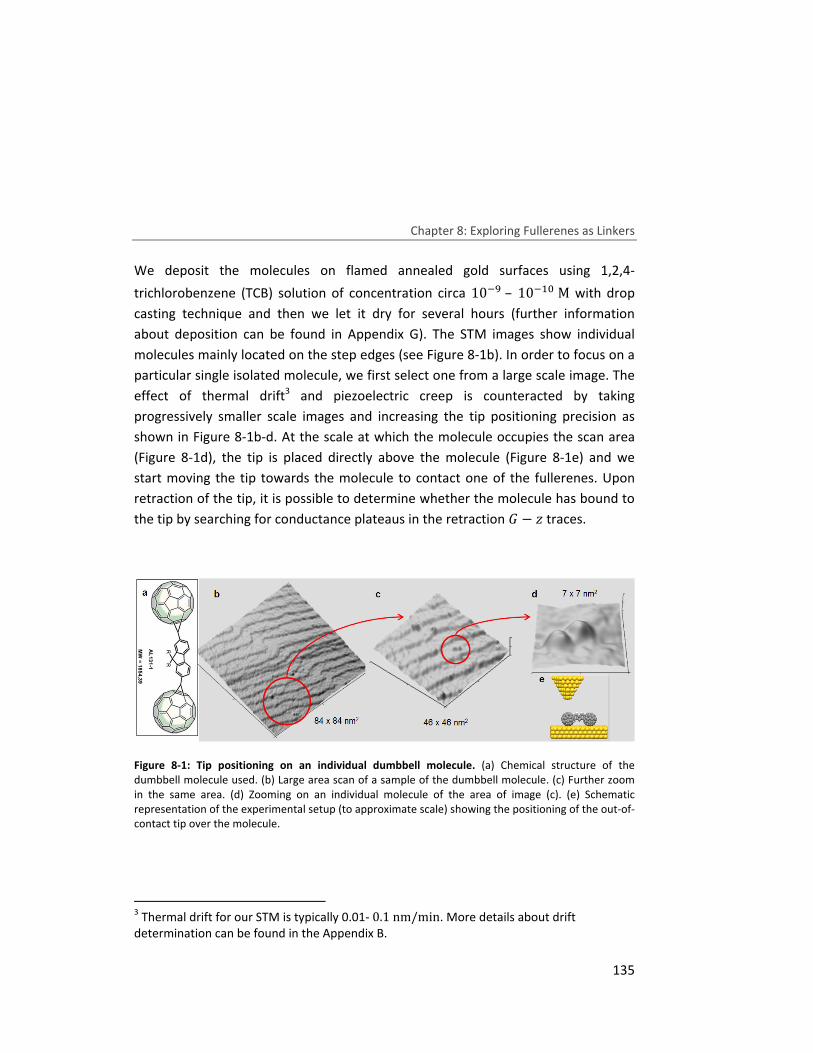
Chapter 8: Exploring Fullerenes as Linkers
135
We deposit the molecules on flamed annealed gold surfaces using 1,2,4-
trichlorobenzene (TCB) solution of concentration circa 10�Ù–10�' M with drop
casting technique and then we let it dry for several hours (further information
about deposition can be found in Appendix G). The STM images show individual
molecules mainly located on the step edges (see Figure 8-1b). In order to focus on a
particular single isolated molecule, we first select one from a large scale image. The
effect of thermal drift3 and piezoelectric creep is counteracted by taking
progressively smaller scale images and increasing the tip positioning precision as
shown in Figure 8-1b-d. At the scale at which the molecule occupies the scan area
(Figure 8-1d), the tip is placed directly above the molecule (Figure 8-1e) and we
start moving the tip towards the molecule to contact one of the fullerenes. Upon
retraction of the tip, it is possible to determine whether the molecule has bound to
the tip by searching for conductance plateaus in the retraction � − ¿ traces.
Figure 8-1: Tip positioning on an individual dumbbell molecule. (a) Chemical structure of the dumbbell molecule used. (b) Large area scan of a sample of the dumbbell molecule. (c) Further zoom in the same area. (d) Zooming on an individual molecule of the area of image (c). (e) Schematic representation of the experimental setup (to approximate scale) showing the positioning of the out-of-contact tip over the molecule.
3 Thermal drift for our STM is typically 0.01- 0.1nm/min. More details about drift determination can be found in the Appendix B.
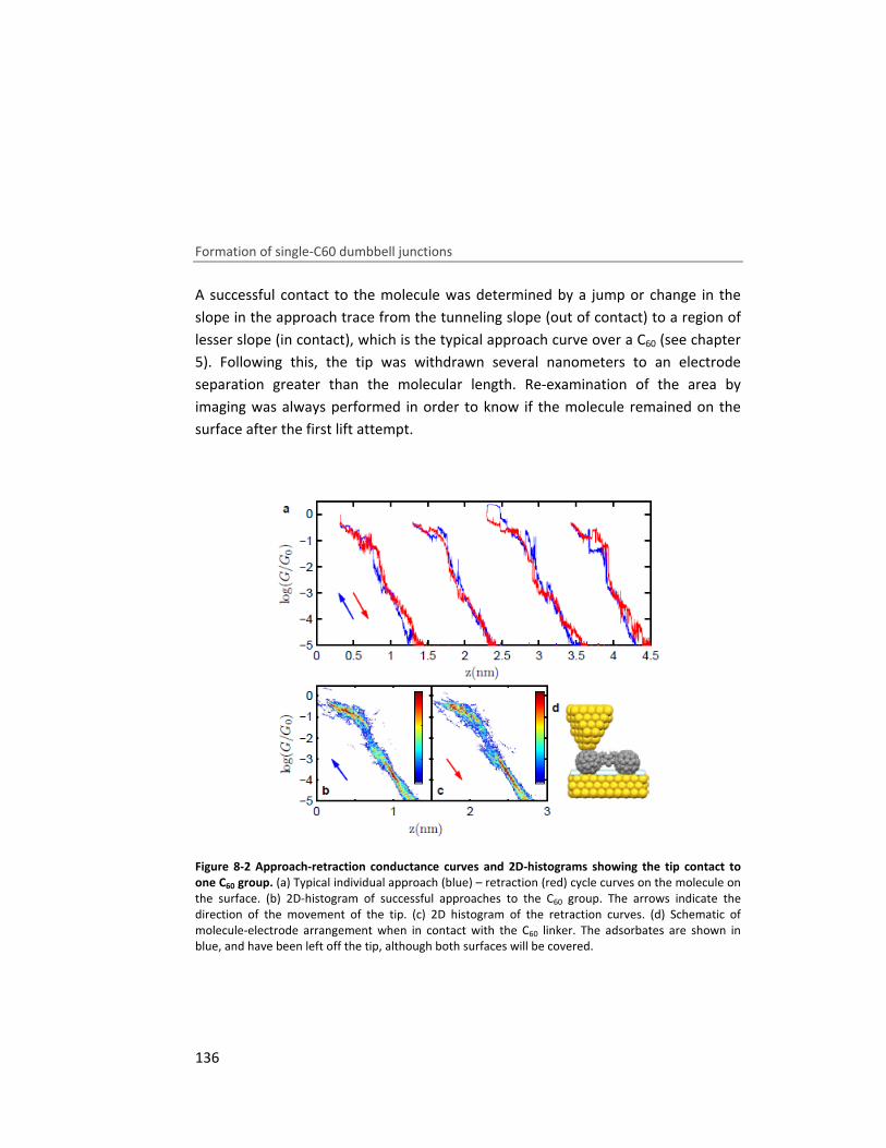
Formation of single-C60 dumbbell junctions
136
A successful contact to the molecule was determined by a jump or change in the
slope in the approach trace from the tunneling slope (out of contact) to a region of
lesser slope (in contact), which is the typical approach curve over a C60 (see chapter
5). Following this, the tip was withdrawn several nanometers to an electrode
separation greater than the molecular length. Re-examination of the area by
imaging was always performed in order to know if the molecule remained on the
surface after the first lift attempt.
Figure 8-2 Approach-retraction conductance curves and 2D-histograms showing the tip contact to
one C60 group. (a) Typical individual approach (blue) – retraction (red) cycle curves on the molecule on the surface. (b) 2D-histogram of successful approaches to the C60 group. The arrows indicate the direction of the movement of the tip. (c) 2D histogram of the retraction curves. (d) Schematic of molecule-electrode arrangement when in contact with the C60 linker. The adsorbates are shown in blue, and have been left off the tip, although both surfaces will be covered.
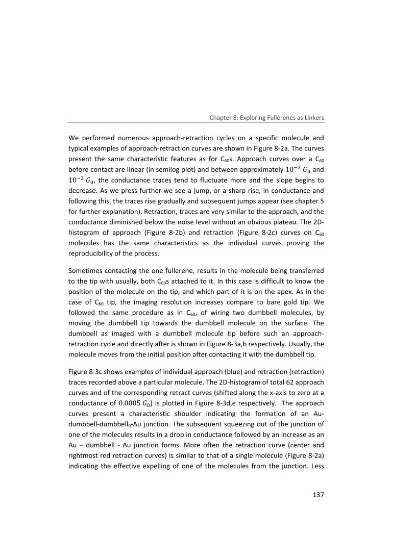
Chapter 8: Exploring Fullerenes as Linkers
137
We performed numerous approach-retraction cycles on a specific molecule and
typical examples of approach-retraction curves are shown in Figure 8-2a. The curves
present the same characteristic features as for C60s. Approach curves over a C60
before contact are linear (in semilog plot) and between approximately 10�N� and 10��� , the conductance traces tend to fluctuate more and the slope begins to
decrease. As we press further we see a jump, or a sharp rise, in conductance and
following this, the traces rise gradually and subsequent jumps appear (see chapter 5
for further explanation). Retraction, traces are very similar to the approach, and the
conductance diminished below the noise level without an obvious plateau. The 2D-
histogram of approach (Figure 8-2b) and retraction (Figure 8-2c) curves on C60
molecules has the same characteristics as the individual curves proving the
reproducibility of the process.
Sometimes contacting the one fullerene, results in the molecule being transferred
to the tip with usually, both C60s attached to it. In this case is difficult to know the
position of the molecule on the tip, and which part of it is on the apex. As in the
case of C60 tip, the imaging resolution increases compare to bare gold tip. We
followed the same procedure as in C60, of wiring two dumbbell molecules, by
moving the dumbbell tip towards the dumbbell molecule on the surface. The
dumbbell as imaged with a dumbbell molecule tip before such an approach-
retraction cycle and directly after is shown in Figure 8-3a,b respectively. Usually, the
molecule moves from the initial position after contacting it with the dumbbell tip.
Figure 8-3c shows examples of individual approach (blue) and retraction (retraction)
traces recorded above a particular molecule. The 2D-histogram of total 62 approach
curves and of the corresponding retract curves (shifted along the x-axis to zero at a
conductance of 0.0005� ) is plotted in Figure 8-3d,e respectively. The approach
curves present a characteristic shoulder indicating the formation of an Au-
dumbbell-dumbbell0-Au junction. The subsequent squeezing out of the junction of
one of the molecules results in a drop in conductance followed by an increase as an
Au – dumbbell - Au junction forms. More often the retraction curve (center and
rightmost red retraction curves) is similar to that of a single molecule (Figure 8-2a)
indicating the effective expelling of one of the molecules from the junction. Less
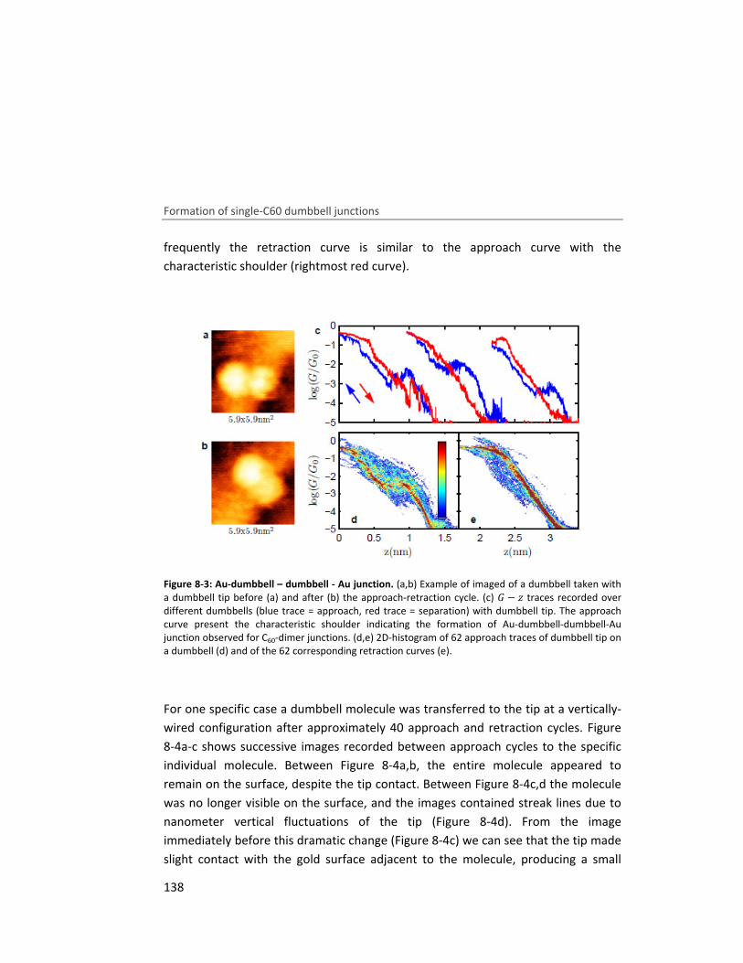
Formation of single-C60 dumbbell junctions
138
frequently the retraction curve is similar to the approach curve with the
characteristic shoulder (rightmost red curve).
Figure 8-3: Au-dumbbell – dumbbell - Au junction. (a,b) Example of imaged of a dumbbell taken with a dumbbell tip before (a) and after (b) the approach-retraction cycle. (c) � − ¿ traces recorded over different dumbbells (blue trace = approach, red trace = separation) with dumbbell tip. The approach curve present the characteristic shoulder indicating the formation of Au-dumbbell-dumbbell-Au junction observed for C60-dimer junctions. (d,e) 2D-histogram of 62 approach traces of dumbbell tip on a dumbbell (d) and of the 62 corresponding retraction curves (e).
For one specific case a dumbbell molecule was transferred to the tip at a vertically-
wired configuration after approximately 40 approach and retraction cycles. Figure
8-4a-c shows successive images recorded between approach cycles to the specific
individual molecule. Between Figure 8-4a,b, the entire molecule appeared to
remain on the surface, despite the tip contact. Between Figure 8-4c,d the molecule
was no longer visible on the surface, and the images contained streak lines due to
nanometer vertical fluctuations of the tip (Figure 8-4d). From the image
immediately before this dramatic change (Figure 8-4c) we can see that the tip made
slight contact with the gold surface adjacent to the molecule, producing a small
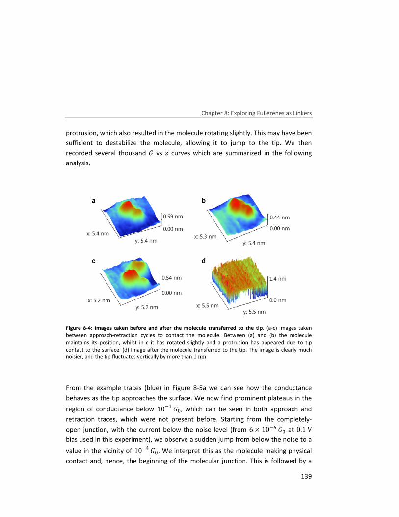
protrusion, which also resulted in the molecule rotating slightly. This may have been
sufficient to destabilize the molecule, allowing it to jump to the tip. We then
recorded several thousand
analysis.
Figure
between approachmaintains its position, whilst in c it has rotated slightly and a protrusion has appeared due to tip contact to the surface. (d) Image after the molecule transferred to the tip. The image is clearly much noisier, and the tip fluctuates vertically by more than
From the example traces (blue) in
behaves as the tip approaches the surface. We now find prominent plateaus i
region of conductance below
retraction traces,
open junction, with the current below the noise level (from
bias used in this experiment), we observe a sudden jump from below the noise to a
value in the vicinity of
contact and, hence, the beginning of the molecular junction. This is followed by a
protrusion, which also resulted in the molecule rotating slightly. This may have been
sufficient to destabilize the molecule, allowing it to jump to the tip. We then
recorded several thousand
analysis.
Figure 8-4: Images taken before and after the molecule transferred to the tip.
between approachmaintains its position, whilst in c it has rotated slightly and a protrusion has appeared due to tip contact to the surface. (d) Image after the molecule transferred to the tip. The image is clearly much
oisier, and the tip fluctuates vertically by more than
From the example traces (blue) in
behaves as the tip approaches the surface. We now find prominent plateaus i
region of conductance below
retraction traces,
open junction, with the current below the noise level (from
as used in this experiment), we observe a sudden jump from below the noise to a
value in the vicinity of
contact and, hence, the beginning of the molecular junction. This is followed by a
protrusion, which also resulted in the molecule rotating slightly. This may have been
sufficient to destabilize the molecule, allowing it to jump to the tip. We then
recorded several thousand �
Images taken before and after the molecule transferred to the tip.
between approach-retraction cycles to contmaintains its position, whilst in c it has rotated slightly and a protrusion has appeared due to tip contact to the surface. (d) Image after the molecule transferred to the tip. The image is clearly much
oisier, and the tip fluctuates vertically by more than
From the example traces (blue) in
behaves as the tip approaches the surface. We now find prominent plateaus i
region of conductance below
retraction traces, which were not present before. Starting from the completely
open junction, with the current below the noise level (from
as used in this experiment), we observe a sudden jump from below the noise to a
value in the vicinity of 10�4contact and, hence, the beginning of the molecular junction. This is followed by a
protrusion, which also resulted in the molecule rotating slightly. This may have been
sufficient to destabilize the molecule, allowing it to jump to the tip. We then � vs ¿ curves which are summarized in the following
Images taken before and after the molecule transferred to the tip.
retraction cycles to contact the molecule. Between maintains its position, whilst in c it has rotated slightly and a protrusion has appeared due to tip contact to the surface. (d) Image after the molecule transferred to the tip. The image is clearly much
oisier, and the tip fluctuates vertically by more than
From the example traces (blue) in Figure
behaves as the tip approaches the surface. We now find prominent plateaus i
region of conductance below 10�1�0, which can be seen in both
which were not present before. Starting from the completely
open junction, with the current below the noise level (from
as used in this experiment), we observe a sudden jump from below the noise to a
�0. We interpr
contact and, hence, the beginning of the molecular junction. This is followed by a
Chapter
protrusion, which also resulted in the molecule rotating slightly. This may have been
sufficient to destabilize the molecule, allowing it to jump to the tip. We then
curves which are summarized in the following
Images taken before and after the molecule transferred to the tip.
act the molecule. Between maintains its position, whilst in c it has rotated slightly and a protrusion has appeared due to tip contact to the surface. (d) Image after the molecule transferred to the tip. The image is clearly much
oisier, and the tip fluctuates vertically by more than 1nm.
Figure 8-5a we can see how the conductance
behaves as the tip approaches the surface. We now find prominent plateaus i
which can be seen in both
which were not present before. Starting from the completely
open junction, with the current below the noise level (from
as used in this experiment), we observe a sudden jump from below the noise to a
e interpret this as the molecule making
contact and, hence, the beginning of the molecular junction. This is followed by a
Chapter 8: Exploring Fullerenes as Linkers
protrusion, which also resulted in the molecule rotating slightly. This may have been
sufficient to destabilize the molecule, allowing it to jump to the tip. We then
curves which are summarized in the following
Images taken before and after the molecule transferred to the tip.
act the molecule. Between (a) and maintains its position, whilst in c it has rotated slightly and a protrusion has appeared due to tip contact to the surface. (d) Image after the molecule transferred to the tip. The image is clearly much
a we can see how the conductance
behaves as the tip approaches the surface. We now find prominent plateaus i
which can be seen in both
which were not present before. Starting from the completely
open junction, with the current below the noise level (from 6 ¡as used in this experiment), we observe a sudden jump from below the noise to a
et this as the molecule making
contact and, hence, the beginning of the molecular junction. This is followed by a
Exploring Fullerenes as Linkers
protrusion, which also resulted in the molecule rotating slightly. This may have been
sufficient to destabilize the molecule, allowing it to jump to the tip. We then
curves which are summarized in the following
Images taken before and after the molecule transferred to the tip. (a-c) Images taken and (b) the molecule
maintains its position, whilst in c it has rotated slightly and a protrusion has appeared due to tip contact to the surface. (d) Image after the molecule transferred to the tip. The image is clearly much
a we can see how the conductance
behaves as the tip approaches the surface. We now find prominent plateaus in the
which can be seen in both approach and
which were not present before. Starting from the completely10�� at 0as used in this experiment), we observe a sudden jump from below the noise to a
et this as the molecule making physical
contact and, hence, the beginning of the molecular junction. This is followed by a
Exploring Fullerenes as Linkers
139
protrusion, which also resulted in the molecule rotating slightly. This may have been
sufficient to destabilize the molecule, allowing it to jump to the tip. We then
curves which are summarized in the following
) Images taken the molecule
maintains its position, whilst in c it has rotated slightly and a protrusion has appeared due to tip contact to the surface. (d) Image after the molecule transferred to the tip. The image is clearly much
a we can see how the conductance
n the
approach and
which were not present before. Starting from the completely-0.1V
as used in this experiment), we observe a sudden jump from below the noise to a
physical
contact and, hence, the beginning of the molecular junction. This is followed by a

Formation of single-C60 dumbbell junctions
140
plateau region in which the conductance rises gradually by less than one order of
magnitude over a distance of 6-8 Å. This we call the low-conductance state, above
which we see the conductance behaving in one of several ways. Following the
plateau, mostly we observe a sharp increase in the slope, which becomes equal to
that above the dumbbell-free areas of gold (blue curve 4 in Figure 8-5a).
Alternatively, with less frequency we see a jump from the low-conductance region
to a second, higher plateau region of conductance where the slope is also low (blue
curves 1,3 in Figure 8-5a). Above this region there is also a clear tunneling region
which extends, in some cases, beyond 1 ¡�0.
Figure 8-5 : Data showing the dumbbell, suspended from the tip, approaching and retracting from
the surface. (a) Examples of typical approach traces (blue) and retraction traces (red). (b) 2D-histogram combining all 3700 approach traces. (c) 2D-histogram combining all 3700 retraction curves. Bias voltage = 0.1 V.
Chapter 8: Exploring Fullerenes as Linkers
141
Upon retracting the tip, we also observe different breaking sequences (see red
traces in Figure 8-5a). In those cases in which the high-conductance state was
present in the approach, we always observe a plateau in the same high-
conductance region in the retraction. The plateaus are, however, significantly
longer than in the approach. At the end of these plateaus, the conductance drops
sharply, either directly to the noise (red curve 3 Figure 8-5a), or, as in the majority
of cases, to a lower region of conductance similar to that observed on initial contact
in the approach (red curve 1,3 Figure 8-5a). Upon further retraction, these traces
extend several more Angstroms in the low-conductance state before, finally, the
molecular junction breaks and the conductance drops sharply below the noise.
When there was no jump to the high-conductance state in the approach trace, the
subsequent retraction traces either appear identical to the approach (curve 2 in
Figure 8-5a), containing only the low-conductance plateaus, or they also contain a
plateau in the high-conductance state (curve 4 in Figure 8-5a).
In total 3,700 complete approach-retraction cycles were performed, until the signal
disappeared, indicating that the molecule had become displaced from the tip. We
have compiled all the approach and retraction traces for which the molecule was
suspended from the tip into separate 2D-histograms without any selection, which
are shown in Figure 8-5b,c respectively. The traces were shifted to zero along the x-
axis at a conductance of 10−1�0 before building the histograms. The histogram of
the approach traces (Figure 8-5b) shows clearly that in the majority of approaches,
the conductance increase monotonically above the low conductance state as far as 1� . The high conductance state is visible as a small green protrusion around 10−2�0, highlighting its low probability in the approach. Contrastingly, the 2D-
histogram of the retraction traces (Figure 8-5c) shows that the high conductance
state is much more prominent when retracting the tip. The histogram highlights
that the high state tends to decrease slightly in conductance with increasing
electrode separation, as does the low state.
Clearly, these results show that there are two stable states of the junction which
are not totally dependent on the absolute tip-position, as the hysteresis shows, but
that they do not occur at any random position. From the appearance of the image
in Figure 8-4d, we can infer that one side of the molecule is strongly bonded to the
Formation of single-C60 dumbbell junctions
142
tip, leaving the other weakly bonded or freely suspended. This implies that the
binding to the tip is relatively constant from one curve to another, so that the
process responsible for the two states most likely takes place on the surface side of
the junction.
Next, above the regions of conductance where plateaus develop (in both the
approach and retraction traces), the tunneling region of the traces extends past 0.1� , even going slightly above 1 � in some cases. This is the range of
conductance seen for the Au-C60-Au junctions, as shown in Figure 8-2a-e, when we
made contact to the fullerene anchor. However, with the molecule now located on
the tip, there is no evidence of the formation of such junctions. This strongly
suggests that the molecule is indeed not at the very apex of the tip, but situated
just to one side. This binding geometry would allow the molecule to bind to the
surface, but also allow Au-Au tunneling to dominate at close distances, as the
molecule becomes squashed.
Due to the fact that the conductance beyond 0. 1� is dominated by Au-Au
tunneling, we can, therefore, estimate that the electrode separation at the point of
closet approach is in the range 2-4 Å. This means the actual tip-substrate separation
at the end of the high-plateau state should be between at least 1.2 to 1.4nm, and
1.6 to 1.8nm in the case of the low state. The length of the fully stretched molecule
is between 2.2nm and 2.3nm. Hence, the discrepancy between the molecular
length and the observed mean breaking distances agrees well with part of the
molecule being adsorbed to the side of the tip. This also means we can rule out the
possibility that the high conductance corresponds only to a single C60 as the
conductance is at least one order of magnitude lower than measured previously for
contact to the C60, and the distance at maximum separation is too great.
Chapter 8: Exploring Fullerenes as Linkers
143
8.3 DFT calculations on the single-C60 dumbbell junction
In order, therefore, to explain these observations, density functional calculations
were carried out followed by a non-equilibrium Green's function scattering
approach to investigate the transport, by the group of Prof. C.J. Lambert at
Lancaster University). Here we summarize some of their results [Gillemot2013].
They investigated three models which are summarized as following:
The first model that was investigated is shown in Figure 8-6a and involves pulling
the molecule up with the tip attached to one of the C60 groups. The resulting
conductance trace shows a plateau region, below 10−5�0, which is lower than the
experimental value (see Figure 8-6b). Furthermore, no switching mechanism
between high and low conductance values appears.
The second model that was checked is shown in Figure 8-6c where the current
bypasses the tip-bound C60 and is injected directly into the fluorene backbone. In
Figure 8-6e (red trace) we can see that this geometry results in a conductance of 10−2�0 which is close to the experimental high state. Although this model explains
the high conductance state observed in the experiment, it still doesn’t explain the
low conductance state. The possibility that the low-conductance state could
correspond simply to conductance across the whole molecule with the molecule
strongly fixed to the side of the tip is not likely, because direct charge injection to
the fluorene would occur.
The third model checked is shown in Figure 8-6d and includes an extra adsorbed
molecule (1, 2, 4-trichlorobenzene (TCB), which was used to deposit the molecule)
between the surface-side C60 anchor group and the gold surface. Hence, it considers
that the low-conductance state corresponds to the surface-side C60 in a ‘pre-gold
contact’ position, sitting atop the layer of adsorbates on the surface. The resulting
conductance trace in the presence of an adsorbate molecule is shown in Figure 8-6e
(black trace). As shown when an adsorbate is inserted into the gap between the
lower C60 and the substrate, the conductance is lower than the relaxed situation
without the solvent molecule. In the experiments, we expect that as the dumbbell is
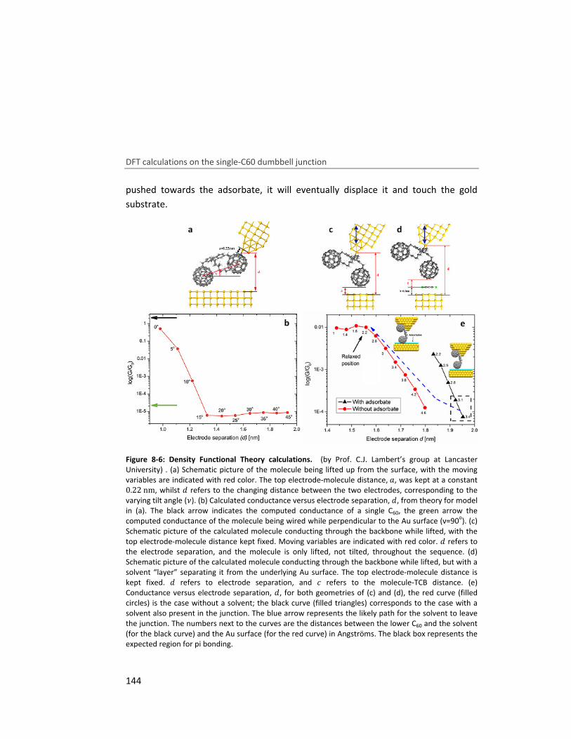
DFT calculations on the single-C60 dumbbell junction
144
pushed towards the adsorbate, it will eventually displace it and touch the gold
substrate.
Figure 8-6: Density Functional Theory calculations. (by Prof. C.J. Lambert’s group at Lancaster University) . (a) Schematic picture of the molecule being lifted up from the surface, with the moving variables are indicated with red color. The top electrode-molecule distance,�, was kept at a constant 0.22nm, whilst � refers to the changing distance between the two electrodes, corresponding to the varying tilt angle (�). (b) Calculated conductance versus electrode separation, �, from theory for model in (a). The black arrow indicates the computed conductance of a single C60, the green arrow the computed conductance of the molecule being wired while perpendicular to the Au surface (ν=90o). (c) Schematic picture of the calculated molecule conducting through the backbone while lifted, with the top electrode-molecule distance kept fixed. Moving variables are indicated with red color. � refers to the electrode separation, and the molecule is only lifted, not tilted, throughout the sequence. (d) Schematic picture of the calculated molecule conducting through the backbone while lifted, but with a solvent “layer” separating it from the underlying Au surface. The top electrode-molecule distance is kept fixed. � refers to electrode separation, and È refers to the molecule-TCB distance. (e) Conductance versus electrode separation, �, for both geometries of (c) and (d), the red curve (filled circles) is the case without a solvent; the black curve (filled triangles) corresponds to the case with a solvent also present in the junction. The blue arrow represents the likely path for the solvent to leave the junction. The numbers next to the curves are the distances between the lower C60 and the solvent (for the black curve) and the Au surface (for the red curve) in Angströms. The black box represents the expected region for pi bonding.
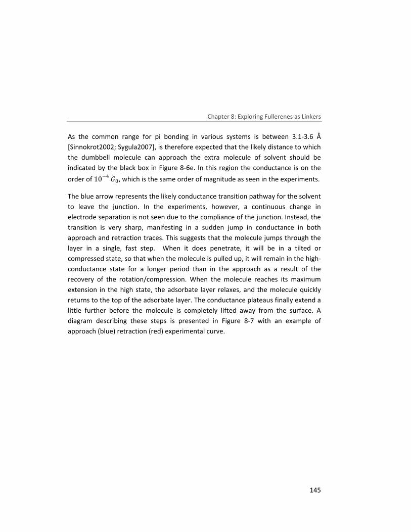
Chapter 8: Exploring Fullerenes as Linkers
145
As the common range for pi bonding in various systems is between 3.1-3.6 Å
[Sinnokrot2002; Sygula2007], is therefore expected that the likely distance to which
the dumbbell molecule can approach the extra molecule of solvent should be
indicated by the black box in Figure 8-6e. In this region the conductance is on the
order of 10−4�0, which is the same order of magnitude as seen in the experiments.
The blue arrow represents the likely conductance transition pathway for the solvent
to leave the junction. In the experiments, however, a continuous change in
electrode separation is not seen due to the compliance of the junction. Instead, the
transition is very sharp, manifesting in a sudden jump in conductance in both
approach and retraction traces. This suggests that the molecule jumps through the
layer in a single, fast step. When it does penetrate, it will be in a tilted or
compressed state, so that when the molecule is pulled up, it will remain in the high-
conductance state for a longer period than in the approach as a result of the
recovery of the rotation/compression. When the molecule reaches its maximum
extension in the high state, the adsorbate layer relaxes, and the molecule quickly
returns to the top of the adsorbate layer. The conductance plateaus finally extend a
little further before the molecule is completely lifted away from the surface. A
diagram describing these steps is presented in Figure 8-7 with an example of
approach (blue) retraction (red) experimental curve.
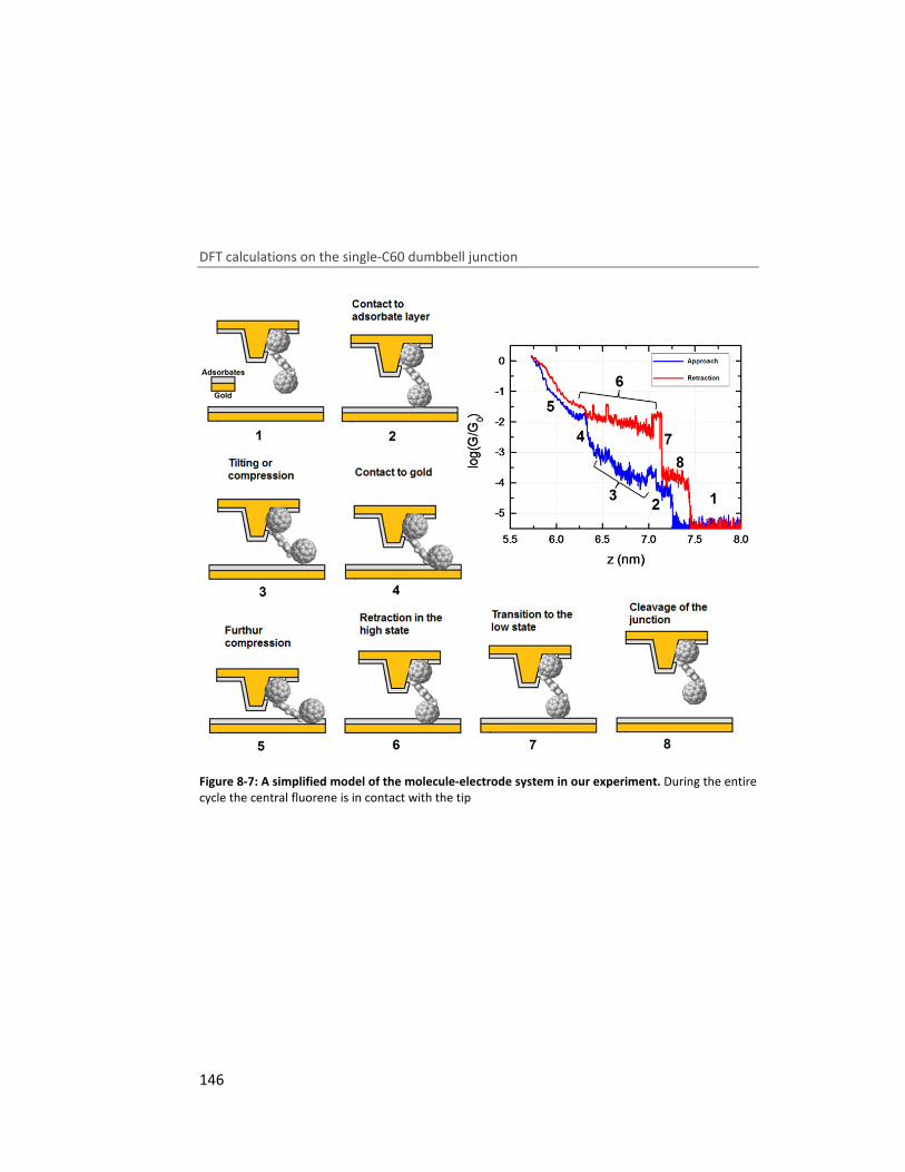
DFT calculations on the single-C60 dumbbell junction
146
Figure 8-7: A simplified model of the molecule-electrode system in our experiment. During the entire cycle the central fluorene is in contact with the tip
Chapter 8: Exploring Fullerenes as Linkers
147
8.4 Conclusions
In conclusion, we have investigated the junction formation and conductance of an
isolated fullerene dumbbell molecule. By pressing the STM tip onto one of the C60
anchor groups, this sometimes results in the molecule being transferred to the tip.
For one specific case the dumbbell was transferred to the tip at a vertically-wired
configuration. With the molecule lifted we observed two main conductance states,
a high conductance state close to 10��� and a lower state close to 10�� . The
theoretical calculations strongly suggest that the high conductance state
corresponds to current injection directly into the fluorine bridge, thus the molecule
is bound by the fluorine instead of the C60. The low conductance state can be
explained by a solvent monolayer, trapped between the surface and one C60 group,
causing a dramatic reduction in the conductance.
References
148
References
[Arroyo2011] Arroyo, C. R., E. Leary, A. Castellanos-Gómez, G. Rubio-Bollinger, M. T.
González, et al. (2011). "Influence of Binding Groups on Molecular Junction Formation." Journal of the American Chemical Society 133(36): 14313-14319.
[Atienza-Castellanos2007] Atienza-Castellanos, C., M. Wielopolski, D. M. Guldi, C. van der Pol, M. R. Bryce, et al. (2007). "Determination of the attenuation factor in fluorene-based molecular wires." Chemical Communications(48): 5164-5166.
[Bilan2012] Bilan, S., L. A. Zotti, F. Pauly and J. C. Cuevas (2012). "Theoretical study of the charge transport through C_{60}-based single-molecule junctions." Physical Review B 85(20): 205403.
[Eiermann1995] Eiermann, M., R. C. Haddon, B. Knight, Q. C. Li, M. Maggini, et al. (1995). "Electrochemical Evidence for Through-Space Orbital Interactions in Spiromethanofullerenes." Angewandte Chemie International Edition in English 34(15): 1591-1594.
[French2012] French, W. R., C. R. Iacovella and P. T. Cummings (2012). "Large-Scale Atomistic Simulations of Environmental Effects on the Formation and Properties of Molecular Junctions." ACS Nano 6(3): 2779-2789.
[Gillemot2013] Gillemot, K., C. Evangeli, E. Leary, A. La Rosa, M. T. González, et al. (2013). "A Detailed Experimental and Theoretical Study into the Properties of C60 Dumbbell Junctions." Small 9(22): 3812-3822.
[Hong2011] Hong, W., D. Z. Manrique, P. Moreno-García, M. Gulcur, A. Mishchenko, et al. (2011). "Single Molecular Conductance of Tolanes: Experimental and Theoretical Study on the Junction Evolution Dependent on the Anchoring Group." Journal of the American Chemical Society 134(4): 2292-2304.
[Kockmann2009] Kockmann, D., B. Poelsema and H. J. W. Zandvliet (2009). "Transport through a Single Octanethiol Molecule." Nano Letters 9(3): 1147-1151.
[Kooistra2010] Kooistra, F. B., T. M. Leuning, E. Maroto Martinez and J. C. Hummelen (2010). "Two new types of [small pi]-conjugation between a fullerene sphere and an addend." Chemical Communications 46(12): 2097-2099.
[Kumar2012] Kumar, A., R. Heimbuch, B. Poelsema and Z. H. J. W (2012). "Controlled transport through a single molecule." J. Phys. Condens. Matter 24(8).
Chapter 8: Exploring Fullerenes as Linkers
149
[Lafferentz2009] Lafferentz, L., F. Ample, H. Yu, S. Hecht, C. Joachim, et al. (2009). "Conductance of a Single Conjugated Polymer as a Continuous Function of Its Length." Science 323(5918): 1193-1197.
[Leary2011] Leary, E., M. T. González, C. van der Pol, M. R. Bryce, S. Filippone, et al. (2011). "Unambiguous One-Molecule Conductance Measurements under Ambient Conditions." Nano Letters 11(6): 2236-2241.
[Leary2009] Leary, E., H. Van Zalinge, S. J. Higgins, R. J. Nichols, F. Fabrizi de Biani, et al. (2009). "A molecular wire incorporating a robust hexanuclear platinum cluster." Physical Chemistry Chemical Physics 11(25): 5198-5202.
[Lörtscher2007] Lörtscher, E., H. B. Weber and H. Riel (2007). "Statistical Approach to Investigating Transport through Single Molecules." Physical Review Letters 98(17): 176807.
[Martin2008] Martin, C. A., D. Ding, J. K. Sørensen, T. Bjørnholm, J. M. van Ruitenbeek, et al. (2008). "Fullerene-Based Anchoring Groups for Molecular Electronics." Journal of the American Chemical Society 130(40): 13198-13199.
[Matthias2012] Matthias, K., A. Francisco, J. Christian and G. Leonhard (2012). "Voltage-dependent conductance of a single graphene nanoribbon." Nature Nanotechnology 7(11): 713-717.
[Mishchenko2010] Mishchenko, A., L. A. Zotti, D. Vonlanthen, M. Bürkle, F. Pauly, et al. (2010). "Single-Molecule Junctions Based on Nitrile-Terminated Biphenyls: A Promising New Anchoring Group." Journal of the American Chemical Society 133(2): 184-187.
[Nichols2010] Nichols, R. J., W. Haiss, S. J. Higgins, E. Leary, S. Martin, et al. (2010). "The experimental determination of the conductance of single molecules." Physical Chemistry Chemical Physics 12(12): 2801-2815.
[Reuter2012] Reuter, M. G., M. C. Hersam, T. Seideman and M. A. Ratner (2012). "Signatures of Cooperative Effects and Transport Mechanisms in Conductance Histograms." Nano Letters 12(5): 2243-2248.
[Reuter2011] Reuter, M. G., T. Seideman and M. A. Ratner (2011). "Molecular Conduction through Adlayers: Cooperative Effects Can Help or Hamper Electron Transport." Nano Letters 11(11): 4693-4696.
[Sinnokrot2002] Sinnokrot, M. O., E. F. Valeev and C. D. Sherrill (2002). "Estimates of the Ab Initio Limit for π−π Interactions: The Benzene Dimer." Journal of
the American Chemical Society 124(36): 10887-10893. [Songmei2008] Songmei, W., G. Maria Teresa, H. Roman, G. Sergio, M. Marcel, et al.
(2008). "Molecular junctions based on aromatic coupling." Nature Nanotechnology 3(9): 569-574.
References
150
[Sygula2007] Sygula, A., F. R. Fronczek, R. Sygula, P. W. Rabideau and M. M. Olmstead (2007). "A Double Concave Hydrocarbon Buckycatcher." Journal of the American Chemical Society 129(13): 3842-3843.
[Toher2011] Toher, C., R. Temirov, A. Greuling, F. Pump, M. Kaczmarski, et al. (2011). "Electrical transport through a mechanically gated molecular wire." Physical Review B 83(15): 155402.
[Valkenier2014] Valkenier, H., C. M. Guedon, T. Markussen, K. S. Thygesen, S. J. van der Molen, et al. (2014). "Cross-conjugation and quantum interference: a general correlation?" Physical Chemistry Chemical Physics.
[Velizhanin2009] Velizhanin, K. A., T. A. Zeidan, I. V. Alabugin and S. Smirnov (2009). "Single Molecule Conductance of Bipyridyl Ethynes: The Role of Surface Binding Modes†." The Journal of Physical Chemistry B 114(45): 14189-14193.
[Venkataraman2006] Venkataraman, L., J. E. Klare, I. W. Tam, C. Nuckolls, M. S. Hybertsen, et al. (2006). "Single-Molecule Circuits with Well-Defined Molecular Conductance." Nano Letters 6(3): 458-462.
[Wang2009] Wang, C., A. S. Batsanov, M. R. Bryce, S. Martín, R. J. Nichols, et al. (2009). "Oligoyne Single Molecule Wires." Journal of the American Chemical Society 131(43): 15647-15654.
[Wang2011] Wang, R. N., X. H. Zheng, L. L. Song and Z. Zeng (2011). "First-principles study on electron transport of carbon dumbbells C60-Cn-C60." The Journal of Chemical Physics 135(4): -.
[Xu2003] Xu, B. and N. J. Tao (2003). "Measurement of Single-Molecule Resistance by Repeated Formation of Molecular Junctions." Science 301(5637): 1221-1223.
[Zotti2010] Zotti, L. A., T. Kirchner, J.-C. Cuevas, F. Pauly, T. Huhn, et al. (2010). "Revealing the Role of Anchoring Groups in the Electrical Conduction Through Single-Molecule Junctions." Small 6(14): 1529-1535.
In this thesis scanning tunneling microscopy has been used to study
thermoelectricity in molecular junctions at the
routes to increase thermoelectric performance in these junc
A novel
molecu
capabilities of a Scanning Tunneling Microscope (STM) to enable the simultaneous
measurement
evolution of a molecular junction.
opens the way to in situ engineering of the thermoelectric performance of
molecular junctions.
The power of
the enhancement of thermopo
contrast to previously reported experimental results, by imaging the sample prior to
junction formation, the exact
formed single
simultaneously, the thermopower and conductance during the whole evolution of
the junction. We observed that the thermopower of a C
by coupling two C
show that the thermopower can be further doubled by coupling to a third C
figure of merit
respectively with respect to one C
engineering the thermopower of a molecular junction by mechanical manipulation.
The role of the electronic s
metallic contacts
investigating how thermoelectricity is continuously modified from bulk all the way
down to the atomic scale where quantum
thermopower, changes not only its magnitude but also its sign when the contact
size dimensions are reduced to the size of a single atom. Moreover, we find that in
In this thesis scanning tunneling microscopy has been used to study
thermoelectricity in molecular junctions at the
routes to increase thermoelectric performance in these junc
novel powerful
molecule junctions has been developed
capabilities of a Scanning Tunneling Microscope (STM) to enable the simultaneous
measurement of electrical transport and thermopower during the formation and
evolution of a molecular junction.
opens the way to in situ engineering of the thermoelectric performance of
molecular junctions.
The power of this technique was
the enhancement of thermopo
contrast to previously reported experimental results, by imaging the sample prior to
junction formation, the exact
formed single-
simultaneously, the thermopower and conductance during the whole evolution of
the junction. We observed that the thermopower of a C
by coupling two C
show that the thermopower can be further doubled by coupling to a third C
figure of merit
respectively with respect to one C
engineering the thermopower of a molecular junction by mechanical manipulation.
The role of the electronic s
metallic contacts
investigating how thermoelectricity is continuously modified from bulk all the way
down to the atomic scale where quantum
thermopower, changes not only its magnitude but also its sign when the contact
size dimensions are reduced to the size of a single atom. Moreover, we find that in
In this thesis scanning tunneling microscopy has been used to study
thermoelectricity in molecular junctions at the
routes to increase thermoelectric performance in these junc
powerful experimental technique to measure the thermopower of single
le junctions has been developed
capabilities of a Scanning Tunneling Microscope (STM) to enable the simultaneous
of electrical transport and thermopower during the formation and
evolution of a molecular junction.
opens the way to in situ engineering of the thermoelectric performance of
molecular junctions.
this technique was
the enhancement of thermopo
contrast to previously reported experimental results, by imaging the sample prior to
junction formation, the exact
- and double
simultaneously, the thermopower and conductance during the whole evolution of
the junction. We observed that the thermopower of a C
by coupling two C60 molecules. DFT
show that the thermopower can be further doubled by coupling to a third C
figure of merit � shows a 4
respectively with respect to one C
engineering the thermopower of a molecular junction by mechanical manipulation.
The role of the electronic structure in determining the thermopower
metallic contacts was evidenced.
investigating how thermoelectricity is continuously modified from bulk all the way
down to the atomic scale where quantum
thermopower, changes not only its magnitude but also its sign when the contact
size dimensions are reduced to the size of a single atom. Moreover, we find that in
In this thesis scanning tunneling microscopy has been used to study
thermoelectricity in molecular junctions at the
routes to increase thermoelectric performance in these junc
experimental technique to measure the thermopower of single
le junctions has been developed.
capabilities of a Scanning Tunneling Microscope (STM) to enable the simultaneous
of electrical transport and thermopower during the formation and
evolution of a molecular junction. This work goes beyond the
opens the way to in situ engineering of the thermoelectric performance of
this technique was demonstrated, in particular, in C
the enhancement of thermopower by molecular manipulation was
contrast to previously reported experimental results, by imaging the sample prior to
junction formation, the exact number of molecules in the junction is known. We
and double-C60 junctions controllably and we measured
simultaneously, the thermopower and conductance during the whole evolution of
the junction. We observed that the thermopower of a C
molecules. DFT-based calculations by
show that the thermopower can be further doubled by coupling to a third C
shows a 4-fold and a 16
respectively with respect to one C60. Our results demonstrate the possibility of
engineering the thermopower of a molecular junction by mechanical manipulation.
tructure in determining the thermopower
evidenced. This system offers the unique possibility of
investigating how thermoelectricity is continuously modified from bulk all the way
down to the atomic scale where quantum
thermopower, changes not only its magnitude but also its sign when the contact
size dimensions are reduced to the size of a single atom. Moreover, we find that in
In this thesis scanning tunneling microscopy has been used to study
thermoelectricity in molecular junctions at the fundamental level and explore
routes to increase thermoelectric performance in these junc
experimental technique to measure the thermopower of single
. This technique
capabilities of a Scanning Tunneling Microscope (STM) to enable the simultaneous
of electrical transport and thermopower during the formation and
This work goes beyond the
opens the way to in situ engineering of the thermoelectric performance of
demonstrated, in particular, in C
wer by molecular manipulation was
contrast to previously reported experimental results, by imaging the sample prior to
number of molecules in the junction is known. We
junctions controllably and we measured
simultaneously, the thermopower and conductance during the whole evolution of
the junction. We observed that the thermopower of a C
based calculations by
show that the thermopower can be further doubled by coupling to a third C
fold and a 16-fold increase, for two and t
Our results demonstrate the possibility of
engineering the thermopower of a molecular junction by mechanical manipulation.
tructure in determining the thermopower
This system offers the unique possibility of
investigating how thermoelectricity is continuously modified from bulk all the way
down to the atomic scale where quantum effects dominate. We found that
thermopower, changes not only its magnitude but also its sign when the contact
size dimensions are reduced to the size of a single atom. Moreover, we find that in
General Conclusions
In this thesis scanning tunneling microscopy has been used to study
fundamental level and explore
routes to increase thermoelectric performance in these junctions.
experimental technique to measure the thermopower of single
This technique expands the instrumental
capabilities of a Scanning Tunneling Microscope (STM) to enable the simultaneous
of electrical transport and thermopower during the formation and
This work goes beyond the-state
opens the way to in situ engineering of the thermoelectric performance of
demonstrated, in particular, in C60
wer by molecular manipulation was
contrast to previously reported experimental results, by imaging the sample prior to
number of molecules in the junction is known. We
junctions controllably and we measured
simultaneously, the thermopower and conductance during the whole evolution of
the junction. We observed that the thermopower of a C60 molecule can be doubled
based calculations by Prof. C.J. Lambert
show that the thermopower can be further doubled by coupling to a third C
fold increase, for two and t
Our results demonstrate the possibility of
engineering the thermopower of a molecular junction by mechanical manipulation.
tructure in determining the thermopower
This system offers the unique possibility of
investigating how thermoelectricity is continuously modified from bulk all the way
effects dominate. We found that
thermopower, changes not only its magnitude but also its sign when the contact
size dimensions are reduced to the size of a single atom. Moreover, we find that in
General Conclusions
In this thesis scanning tunneling microscopy has been used to study
fundamental level and explore
experimental technique to measure the thermopower of single
expands the instrumental
capabilities of a Scanning Tunneling Microscope (STM) to enable the simultaneous
of electrical transport and thermopower during the formation and
state-of-the-art and
opens the way to in situ engineering of the thermoelectric performance of
60 junctions where
wer by molecular manipulation was shown
contrast to previously reported experimental results, by imaging the sample prior to
number of molecules in the junction is known. We
junctions controllably and we measured
simultaneously, the thermopower and conductance during the whole evolution of
ecule can be doubled
C.J. Lambert’s group
show that the thermopower can be further doubled by coupling to a third C60. The
fold increase, for two and three C
Our results demonstrate the possibility of
engineering the thermopower of a molecular junction by mechanical manipulation.
tructure in determining the thermopower in nanoscale
This system offers the unique possibility of
investigating how thermoelectricity is continuously modified from bulk all the way
effects dominate. We found that
thermopower, changes not only its magnitude but also its sign when the contact
size dimensions are reduced to the size of a single atom. Moreover, we find that in
General Conclusions
151
In this thesis scanning tunneling microscopy has been used to study
fundamental level and explore
experimental technique to measure the thermopower of single-
expands the instrumental
capabilities of a Scanning Tunneling Microscope (STM) to enable the simultaneous
of electrical transport and thermopower during the formation and
art and
opens the way to in situ engineering of the thermoelectric performance of
junctions where
shown. In
contrast to previously reported experimental results, by imaging the sample prior to
number of molecules in the junction is known. We
junctions controllably and we measured
simultaneously, the thermopower and conductance during the whole evolution of
ecule can be doubled
group
. The
ree C60s
Our results demonstrate the possibility of
engineering the thermopower of a molecular junction by mechanical manipulation.
nanoscale of
This system offers the unique possibility of
investigating how thermoelectricity is continuously modified from bulk all the way
effects dominate. We found that the
thermopower, changes not only its magnitude but also its sign when the contact
size dimensions are reduced to the size of a single atom. Moreover, we find that in
General Conclusions
152
the case of gold, the thermopower of a few-atom contact exhibits a series of
minima correlated with the maxima of the conductance, in marked contrast with
the platinum wires where such oscillations are absent. Coherent transport
theoretical calculations by Prof. J.C. Cuevas’ group, demonstrate that the different
behaviour of the two metals can be explained in terms of their different electronic
structure.
Furthermore, the enhancement of the thermopower without affecting the
conductance by modifying the chemical structure of OPEs molecules was
demonstrated. More specifically, by incorporating a dithiafulvalene unit to the OPE
backbone, we introduce a Fano resonance in the transmission spectrum close to the
Fermi level. Introducing a second unit moves the Fano resonance closer to the
Fermi level, enhancing the Seebeck coefficient. In contrast, previous strategies
suggested for improving the thermopower, were also causing modification of
conductance. We have also observed, that the thermopower of a molecular
junction is sensitive to strain increasing as the molecule is stretched.
Finally, the use of C60 as a linker in molecular junctions was explored by
investigating the junction formation and conductance of an isolated fullerene
dumbbell molecule. By pressing the STM tip onto one of the C60 anchor groups, this
sometimes results in the molecule being transferred to the tip. For one specific case
the dumbbell was transferred to the tip at a vertically-wired configuration. With the
molecule lifted we observed two main conductance states; a high conductance
state close to 10−2�0 and a lower state close to 10−4�0. The theoretical
calculations by Prof. C.J. Lambert’s group strongly suggest that the high
conductance state corresponds to current injection directly into the fluorine bridge,
thus the molecules are bound by the fluorine instead of the C60. The low
conductance state can be explained with a solvent monolayer, trapped between the
surface and one C60 group, causing a dramatic reduction in the conductance.
En esta tesis hemos utilizado un microscopio de efecto túnel para estudiar
termoelectricidad en uniones moleculares a nivel fundamental y explorar nuevas
rutas
Se ha desarrolla
thermopower de uniones moleculares formadas por una única molécula. Esta nueva
técnica amplía la capacidad instrumental de un Microscopio de Efecto Túnel (STM)
para permitir la medida simultánea d
la formación y evolución de una unión molecular. Este trabajo va más allá de los
últimos avances en el campo y abre el camino para hacer ingeniería
rendimiento termoeléctrico de
El potencial de esta técnica se ha demostrado, en particular, en uniones de
moléculas C
manipulación molecular. En contraste con resultados experimentales publicados
previamente, mediante la tom
molecular se conoce el número exacto de moléculas en la unión. Se han formado de
manera controlada uniones de C
medido simultáneamente el thermopower y la conducta
evolución de la unión. Hemos observado que el thermopower de una molécula C
puede doblarse mediante el acoplamiento de dos C
por el grupo del Prof. C.J. Lambert muestran que el thermopower puede ser
dobl
comparación con un único fullereno, el factor ‘figure of merit’
veces mayor para dos y tres C
la posibilidad de hacer ingeniería con el thermopower de una unión molecular
mediante manipulación mecánica.
Se ha probado también el papel de la estructur
thermopower en la nanoescala de contactos metálicos. El sistema ofrece la
posibilidad única de investigar cómo se modifica progresivamente la
n esta tesis hemos utilizado un microscopio de efecto túnel para estudiar
termoelectricidad en uniones moleculares a nivel fundamental y explorar nuevas
rutas para incrementar el rendimiento termoeléctrico en estas uniones.
Se ha desarrolla
thermopower de uniones moleculares formadas por una única molécula. Esta nueva
técnica amplía la capacidad instrumental de un Microscopio de Efecto Túnel (STM)
para permitir la medida simultánea d
la formación y evolución de una unión molecular. Este trabajo va más allá de los
últimos avances en el campo y abre el camino para hacer ingeniería
rendimiento termoeléctrico de
El potencial de esta técnica se ha demostrado, en particular, en uniones de
moléculas C60 donde se ha mostrado el incremento del thermopower mediante
manipulación molecular. En contraste con resultados experimentales publicados
previamente, mediante la tom
molecular se conoce el número exacto de moléculas en la unión. Se han formado de
manera controlada uniones de C
medido simultáneamente el thermopower y la conducta
evolución de la unión. Hemos observado que el thermopower de una molécula C
puede doblarse mediante el acoplamiento de dos C
por el grupo del Prof. C.J. Lambert muestran que el thermopower puede ser
doblado de nuevo mediante el acoplamiento de una tercera molécula C
comparación con un único fullereno, el factor ‘figure of merit’
veces mayor para dos y tres C
la posibilidad de hacer ingeniería con el thermopower de una unión molecular
mediante manipulación mecánica.
Se ha probado también el papel de la estructur
thermopower en la nanoescala de contactos metálicos. El sistema ofrece la
posibilidad única de investigar cómo se modifica progresivamente la
n esta tesis hemos utilizado un microscopio de efecto túnel para estudiar
termoelectricidad en uniones moleculares a nivel fundamental y explorar nuevas
para incrementar el rendimiento termoeléctrico en estas uniones.
Se ha desarrollado una innovadora y potente técnica experimental para medir
thermopower de uniones moleculares formadas por una única molécula. Esta nueva
técnica amplía la capacidad instrumental de un Microscopio de Efecto Túnel (STM)
para permitir la medida simultánea d
la formación y evolución de una unión molecular. Este trabajo va más allá de los
últimos avances en el campo y abre el camino para hacer ingeniería
rendimiento termoeléctrico de
El potencial de esta técnica se ha demostrado, en particular, en uniones de
donde se ha mostrado el incremento del thermopower mediante
manipulación molecular. En contraste con resultados experimentales publicados
previamente, mediante la tom
molecular se conoce el número exacto de moléculas en la unión. Se han formado de
manera controlada uniones de C
medido simultáneamente el thermopower y la conducta
evolución de la unión. Hemos observado que el thermopower de una molécula C
puede doblarse mediante el acoplamiento de dos C
por el grupo del Prof. C.J. Lambert muestran que el thermopower puede ser
ado de nuevo mediante el acoplamiento de una tercera molécula C
comparación con un único fullereno, el factor ‘figure of merit’
veces mayor para dos y tres C
la posibilidad de hacer ingeniería con el thermopower de una unión molecular
mediante manipulación mecánica.
Se ha probado también el papel de la estructur
thermopower en la nanoescala de contactos metálicos. El sistema ofrece la
posibilidad única de investigar cómo se modifica progresivamente la
n esta tesis hemos utilizado un microscopio de efecto túnel para estudiar
termoelectricidad en uniones moleculares a nivel fundamental y explorar nuevas
para incrementar el rendimiento termoeléctrico en estas uniones.
do una innovadora y potente técnica experimental para medir
thermopower de uniones moleculares formadas por una única molécula. Esta nueva
técnica amplía la capacidad instrumental de un Microscopio de Efecto Túnel (STM)
para permitir la medida simultánea de transporte eléctrico y thermopower durante
la formación y evolución de una unión molecular. Este trabajo va más allá de los
últimos avances en el campo y abre el camino para hacer ingeniería
rendimiento termoeléctrico de uniones moleculares.
El potencial de esta técnica se ha demostrado, en particular, en uniones de
donde se ha mostrado el incremento del thermopower mediante
manipulación molecular. En contraste con resultados experimentales publicados
previamente, mediante la toma de imágenes antes de la formación de la unión
molecular se conoce el número exacto de moléculas en la unión. Se han formado de
manera controlada uniones de C60 compuestas por una y dos moléculas y se ha
medido simultáneamente el thermopower y la conducta
evolución de la unión. Hemos observado que el thermopower de una molécula C
puede doblarse mediante el acoplamiento de dos C
por el grupo del Prof. C.J. Lambert muestran que el thermopower puede ser
ado de nuevo mediante el acoplamiento de una tercera molécula C
comparación con un único fullereno, el factor ‘figure of merit’
veces mayor para dos y tres C60, respectivamente. Nuestros resultados demuestran
la posibilidad de hacer ingeniería con el thermopower de una unión molecular
mediante manipulación mecánica.
Se ha probado también el papel de la estructur
thermopower en la nanoescala de contactos metálicos. El sistema ofrece la
posibilidad única de investigar cómo se modifica progresivamente la
n esta tesis hemos utilizado un microscopio de efecto túnel para estudiar
termoelectricidad en uniones moleculares a nivel fundamental y explorar nuevas
para incrementar el rendimiento termoeléctrico en estas uniones.
do una innovadora y potente técnica experimental para medir
thermopower de uniones moleculares formadas por una única molécula. Esta nueva
técnica amplía la capacidad instrumental de un Microscopio de Efecto Túnel (STM)
e transporte eléctrico y thermopower durante
la formación y evolución de una unión molecular. Este trabajo va más allá de los
últimos avances en el campo y abre el camino para hacer ingeniería
uniones moleculares.
El potencial de esta técnica se ha demostrado, en particular, en uniones de
donde se ha mostrado el incremento del thermopower mediante
manipulación molecular. En contraste con resultados experimentales publicados
a de imágenes antes de la formación de la unión
molecular se conoce el número exacto de moléculas en la unión. Se han formado de
compuestas por una y dos moléculas y se ha
medido simultáneamente el thermopower y la conducta
evolución de la unión. Hemos observado que el thermopower de una molécula C
puede doblarse mediante el acoplamiento de dos C60
por el grupo del Prof. C.J. Lambert muestran que el thermopower puede ser
ado de nuevo mediante el acoplamiento de una tercera molécula C
comparación con un único fullereno, el factor ‘figure of merit’
, respectivamente. Nuestros resultados demuestran
la posibilidad de hacer ingeniería con el thermopower de una unión molecular
Se ha probado también el papel de la estructura electrónica al determinar el
thermopower en la nanoescala de contactos metálicos. El sistema ofrece la
posibilidad única de investigar cómo se modifica progresivamente la
Conclusiones Generales
n esta tesis hemos utilizado un microscopio de efecto túnel para estudiar
termoelectricidad en uniones moleculares a nivel fundamental y explorar nuevas
para incrementar el rendimiento termoeléctrico en estas uniones.
do una innovadora y potente técnica experimental para medir
thermopower de uniones moleculares formadas por una única molécula. Esta nueva
técnica amplía la capacidad instrumental de un Microscopio de Efecto Túnel (STM)
e transporte eléctrico y thermopower durante
la formación y evolución de una unión molecular. Este trabajo va más allá de los
últimos avances en el campo y abre el camino para hacer ingeniería
El potencial de esta técnica se ha demostrado, en particular, en uniones de
donde se ha mostrado el incremento del thermopower mediante
manipulación molecular. En contraste con resultados experimentales publicados
a de imágenes antes de la formación de la unión
molecular se conoce el número exacto de moléculas en la unión. Se han formado de
compuestas por una y dos moléculas y se ha
medido simultáneamente el thermopower y la conductancia durante toda la
evolución de la unión. Hemos observado que el thermopower de una molécula C
60. Cálculos de DFT realizados
por el grupo del Prof. C.J. Lambert muestran que el thermopower puede ser
ado de nuevo mediante el acoplamiento de una tercera molécula C
comparación con un único fullereno, el factor ‘figure of merit’ �, respectivamente. Nuestros resultados demuestran
la posibilidad de hacer ingeniería con el thermopower de una unión molecular
a electrónica al determinar el
thermopower en la nanoescala de contactos metálicos. El sistema ofrece la
posibilidad única de investigar cómo se modifica progresivamente la
Conclusiones Generales
n esta tesis hemos utilizado un microscopio de efecto túnel para estudiar
termoelectricidad en uniones moleculares a nivel fundamental y explorar nuevas
para incrementar el rendimiento termoeléctrico en estas uniones.
do una innovadora y potente técnica experimental para medir
thermopower de uniones moleculares formadas por una única molécula. Esta nueva
técnica amplía la capacidad instrumental de un Microscopio de Efecto Túnel (STM)
e transporte eléctrico y thermopower durante
la formación y evolución de una unión molecular. Este trabajo va más allá de los
últimos avances en el campo y abre el camino para hacer ingeniería in situ
El potencial de esta técnica se ha demostrado, en particular, en uniones de
donde se ha mostrado el incremento del thermopower mediante
manipulación molecular. En contraste con resultados experimentales publicados
a de imágenes antes de la formación de la unión
molecular se conoce el número exacto de moléculas en la unión. Se han formado de
compuestas por una y dos moléculas y se ha
ncia durante toda la
evolución de la unión. Hemos observado que el thermopower de una molécula C
. Cálculos de DFT realizados
por el grupo del Prof. C.J. Lambert muestran que el thermopower puede ser
ado de nuevo mediante el acoplamiento de una tercera molécula C60 � resulta 4 y 16
, respectivamente. Nuestros resultados demuestran
la posibilidad de hacer ingeniería con el thermopower de una unión molecular
a electrónica al determinar el
thermopower en la nanoescala de contactos metálicos. El sistema ofrece la
posibilidad única de investigar cómo se modifica progresivamente la
Conclusiones Generales
153
n esta tesis hemos utilizado un microscopio de efecto túnel para estudiar
termoelectricidad en uniones moleculares a nivel fundamental y explorar nuevas
do una innovadora y potente técnica experimental para medir
thermopower de uniones moleculares formadas por una única molécula. Esta nueva
técnica amplía la capacidad instrumental de un Microscopio de Efecto Túnel (STM)
e transporte eléctrico y thermopower durante
la formación y evolución de una unión molecular. Este trabajo va más allá de los
in situ del
El potencial de esta técnica se ha demostrado, en particular, en uniones de
donde se ha mostrado el incremento del thermopower mediante
manipulación molecular. En contraste con resultados experimentales publicados
a de imágenes antes de la formación de la unión
molecular se conoce el número exacto de moléculas en la unión. Se han formado de
compuestas por una y dos moléculas y se ha
ncia durante toda la
evolución de la unión. Hemos observado que el thermopower de una molécula C60
. Cálculos de DFT realizados
por el grupo del Prof. C.J. Lambert muestran que el thermopower puede ser
60. En
resulta 4 y 16
, respectivamente. Nuestros resultados demuestran
la posibilidad de hacer ingeniería con el thermopower de una unión molecular
a electrónica al determinar el
thermopower en la nanoescala de contactos metálicos. El sistema ofrece la
posibilidad única de investigar cómo se modifica progresivamente la
Conclusiones Generales
154
termoelectricidad desde el volumen hasta la escala atómica, donde dominan los
efectos cuánticos. Hemos demostrado que el thermopower cambia no sólo de
magnitud, sino también de signo, cuando las dimensiones del contacto se reducen
hasta el tamaño de un único átomo. Además, encontramos que en el caso del oro,
el thermopower de un contacto formado por unos pocos átomos presenta una serie
de mínimos correlacionados con los máximos de conductancia, en un marcado
contraste con los contactos de platino donde dichas oscilaciones no aparecen.
Cálculos teóricos de transporte coherente realizados por el grupo del Prof. J.C.
Cuevas demuestran que el comportamiento diferente de estos dos metales se
puede explicar en términos de sus diferentes estructuras electrónicas.
Además, se ha demostrado el incremento del thermopower sin reducir la
conductancia mediante la modificación de la estructura química de moléculas OPE.
Más concretamente, gracias a la incorporación de un ditiolfulvaleno a la columna
del OPE, introducimos una resonancia Fano en el espectro de transmisión cerca del
nivel de Fermi. Añadir una segunda unidad mueve la resonancia Fano aún más cerca
del nivel de Fermi, aumentando el coeficiente Seebeck. En contraste con estos
resultados, estrategias previas propuestas para mejorar thermopower también
producían una modificación de conductancia. También hemos observado que el
thermopower de una unión molecular es sensible a la tensión, aumentando según
se estira la molécula.
Finalmente, se ha explorado el uso del C60 como enlace en uniones moleculares
mediante la investigación de la formación de la unión y la conductancia de
moléculas dumbbell aisladas. Presionar la punta del STM sobre uno de los grupos de
anclaje C60 a veces resulta en la transferencia de la molécula a la punta. En un caso
específico, el dumbbell es transferido a la punta con una configuración vertical. Con
la molécula alzada en la punta, observamos dos estados principales de
conductancia, un estado de conductancia elevada cercana a 10��� y un estado
más bajo cercano a 10�Ó� . Los cálculos teóricos realizados por el grupo del Prof.
C.J. Lambert sugieren que el estado de alta conductancia corresponde a la inyección
de corriente directamente en el puente de fluorina, por lo que la molécula se enlaza
por la fluorina en lugar del C60. El estado de baja conductancia puede explicarse con
Conclusiones Generales
155
una monocapa de disolvente atrapada entre la superficie y uno de los grupos C60, lo
que provoca una dramática reducción de la conductancia.


157

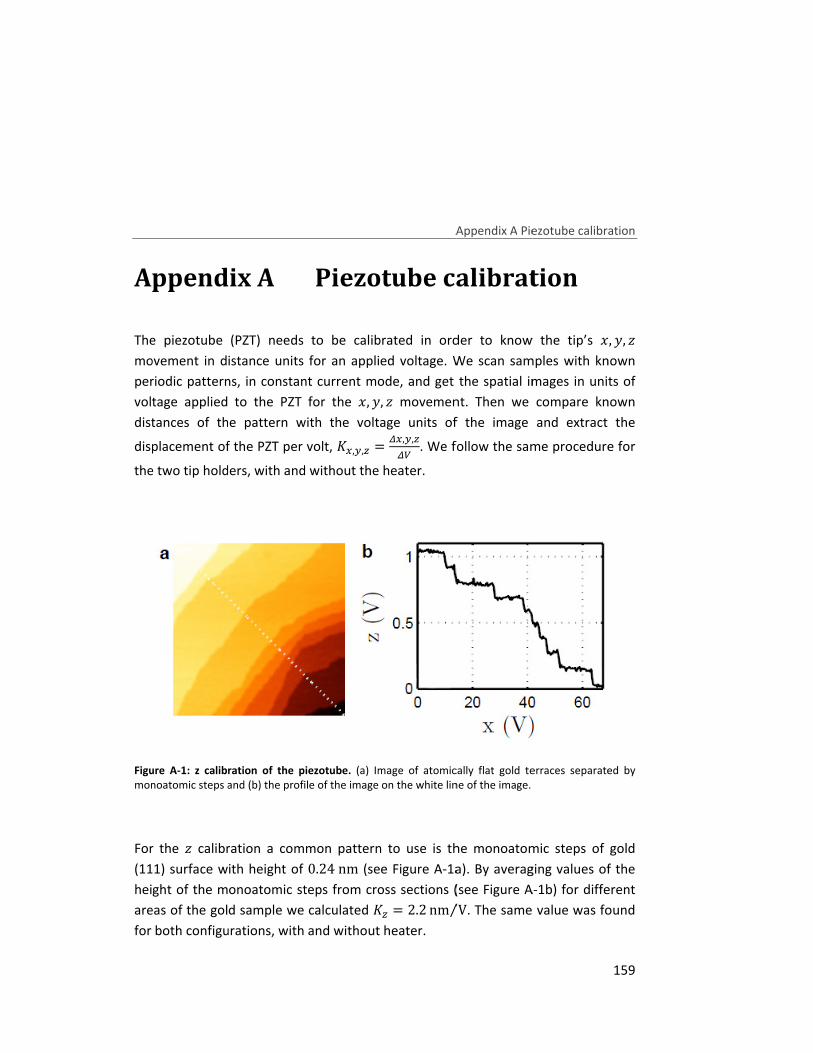
Appendix A
The piezotube (PZT) need
movement in distance units for an applied voltage
periodic patterns, in constant current mode, and get the spatial images in units of
voltage applied to the PZT for the
distances of the pattern with the voltage units of the image and extract the
displacement of the PZT per volt,
the two tip holders, with and without the
Figure A
monoatomic steps and
For the
(111) surface with height of
height of the monoatomic steps
areas of the gold sample we calculated
for both configurations, with and without heater.
Appendix A
The piezotube (PZT) need
movement in distance units for an applied voltage
periodic patterns, in constant current mode, and get the spatial images in units of
voltage applied to the PZT for the
distances of the pattern with the voltage units of the image and extract the
isplacement of the PZT per volt,
the two tip holders, with and without the
Figure A-1: z calibration of the
monoatomic steps and
For the ¿ calibration a common p
(111) surface with height of
height of the monoatomic steps
areas of the gold sample we calculated
for both configurations, with and without heater.
Appendix A
The piezotube (PZT) needs to be calibrated in order to know the tip
movement in distance units for an applied voltage
periodic patterns, in constant current mode, and get the spatial images in units of
voltage applied to the PZT for the
distances of the pattern with the voltage units of the image and extract the
isplacement of the PZT per volt,
the two tip holders, with and without the
calibration of the piezotube
monoatomic steps and (b) the profile of the image on the white line of the image
calibration a common p
(111) surface with height of
height of the monoatomic steps
areas of the gold sample we calculated
for both configurations, with and without heater.
Piezotube
s to be calibrated in order to know the tip
movement in distance units for an applied voltage
periodic patterns, in constant current mode, and get the spatial images in units of
voltage applied to the PZT for the 1, ¾distances of the pattern with the voltage units of the image and extract the
isplacement of the PZT per volt, ��,Á,À �the two tip holders, with and without the
piezotube. (a) Image of atomically flatthe profile of the image on the white line of the image
calibration a common pattern to use
(111) surface with height of 0.24nm (see
height of the monoatomic steps from cross sections (see
areas of the gold sample we calculated �for both configurations, with and without heater.
Appendix A
Piezotube calibration
s to be calibrated in order to know the tip
movement in distance units for an applied voltage. W
periodic patterns, in constant current mode, and get the spatial images in units of , ¿ movement. Then we compare known
distances of the pattern with the voltage units of the image and extract the � Ú�,Á,ÀÚS . We follow the same procedure
the two tip holders, with and without the heater.
mage of atomically flatthe profile of the image on the white line of the image
attern to use is the monoatomic steps of gold
(see Figure A-1a
from cross sections (see �À � 2.2 nm⁄for both configurations, with and without heater.
Appendix A Piezotube calibrati
alibration
s to be calibrated in order to know the tip
We scan samples with known
periodic patterns, in constant current mode, and get the spatial images in units of
movement. Then we compare known
distances of the pattern with the voltage units of the image and extract the
We follow the same procedure
mage of atomically flat gold terraces separated by the profile of the image on the white line of the image.
the monoatomic steps of gold
a). By averaging values of the
from cross sections (see Figure AV⁄ . The same value was found
Piezotube calibrati
alibration
s to be calibrated in order to know the tip’s 1scan samples with known
periodic patterns, in constant current mode, and get the spatial images in units of
movement. Then we compare known
distances of the pattern with the voltage units of the image and extract the
We follow the same procedure
terraces separated by
the monoatomic steps of gold
veraging values of the
Figure A-1b) for different
. The same value was found
Piezotube calibration
159
, ¾, ¿
scan samples with known
periodic patterns, in constant current mode, and get the spatial images in units of
movement. Then we compare known
distances of the pattern with the voltage units of the image and extract the
We follow the same procedure for
terraces separated by
the monoatomic steps of gold
veraging values of the
for different
. The same value was found
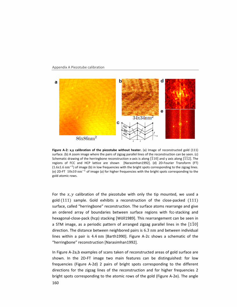
Appendix A Piezotube calibration
160
Figure A-2: x,y calibration of the piezotube without heater. (a) Image of reconstructed gold (111) surface. (b) A zoom image where the pairs of zigzag parallel lines of the reconstruction can be seen. (c) Schematic drawing of the herringbone reconstruction x-axis is along (1l10) and y axis along (1l1l2). The regions of FCC and HCP lattice are shown [Narasimhan1992]. (d) 2D-Fourier Transform (FT) (1.6x1.6nm�') of image (b) in low frequencies with the bright spots corresponding to the zigzag lines. (e) 2D-FT 10x10nm�' of image (a) for higher frequencies with the bright spots corresponding to the gold atomic rows.
For the 1, ¾ calibration of the piezotube with only the tip mounted, we used a
gold(111) sample. Gold exhibits a reconstruction of the close-packed (111) surface, called “herringbone” reconstruction. The surface atoms rearrange and give
an ordered array of boundaries between surface regions with fcc-stacking and
hexagonal-close-pack (hcp) stacking [Wöll1989]. This rearrangement can be seen in
a STM image, as a periodic pattern of arranged zigzag parallel lines in the (11l0) direction. The distance between neighbored pairs is 6.3nm and between individual
lines within a pair is 4.4nm [Barth1990]. Figure A-2c shows a schematic of the
“herringbone” reconstruction [Narasimhan1992].
In Figure A-2a,b examples of scans taken of reconstructed areas of gold surface are
shown. In the 2D-FT image two main features can be distinguished: for low
frequencies (Figure A-2d) 2 pairs of bright spots corresponding to the different
directions for the zigzag lines of the reconstruction and for higher frequencies 2
bright spots corresponding to the atomic rows of the gold (Figure A-2e). The angle
Appendix A Piezotube calibration
161
between the two lines connecting each pair in the low frequencies is 120É and the
distance between them is equal. For the calculation of the 1, ¾ calibration we
measured the distance in several of our images in volt units (volts applied to the
piezotube) between neighboured pairs of the reconstruction. While this distance is
known to be 6.3nm, we extracted ��,Á = 5.1nm V⁄ for the 1, ¾ calibration.
For the 1, ¾ calibration of the configuration with the tip holder with incorporated
heater we used graphene on SiO2. We used the atomic resolution image which was
corrected for thermal drift, shown in Figure A-3b (see Appendix B for the drift
correction). While the spacing of the hexagonal lattice of graphene is known to be
0.246nm [Castro Neto2009], we got ��,Á = 7.58 nm V⁄ .
We can compare this calibration with that obtained of the formulas that already
exist in the literature for the displacement of a PZT with [Yang1998] and without
[Chen1992] the tip mount on it. For a piezoelectric tube the ¿ displacement for an
applied voltage ��, can be calculated with the formula [Chen1992]
where is the length, ℎ is the wall thickness and �N' is the relevant piezoelectric
coefficient of the piezoelectric tube.
The 1 and ¾ deflections of the tube scanner when applying two equal and opposite
voltages on the two opposite quadrants (� = �~�,�Á = −���,�Á) are given by
[Chen1992]:
where Ü is the inner diameter of the piezoelectric tube.
The above formulas don’t take in to account the influence of the tip on the lateral
movement of the PZT. In a STM we are interested in the displacement of the
scanner and thus the displacement of the tip. The tube deflects by bending and the
free end where the tip is mounted is tilted and this will cause a further lateral shift.
Also if the tip is not mounted on the center of the tube then there is a coupling
between ¿ movement and 1, ¾ movement and, as a result, when the tube deflects
�¿ = �N'�À ℎ , Equation A-1
�1, ¾ = 2√2�N'� �|Üℎ , Equation A-2
Appendix A Piezotube calibration
162
in the 1, ¾ direction the ¿ movement of the tip end will vary depending on the
position of the tip with respect to the center of the tube. By applying simple
geometry, the above formulas can be modified to include the effect of the tip to the
displacement [Yang1998]:
where ��,Á = �~�,�Á − ���,�Á and � = 4√2(��N − �'N) (4|(��Ó − �'Ó))� with �' and �� the inner and outer radius of the piezotube respectively. 1m and ¾m is the position
where the tip is mounted on the end of the piezotube with respect to its center,
and
where m is the tip length.
We applied Equation A-3 and Equation A-4 for the calculation of the piezoelectric
constant of our piezotube using the manufacturer parameters ( = 1.62 ×10��m, ℎ = 0.1 × 10��m,�' = 0,85 × 10��m, Ü = 0,95 × 10��m, �N' =1.73 × 10��' m ) [Inc.] and with an average tip length m ≈ 0.3 × 10��m we
found �À = 2.82 nm V⁄ , ��,Á = 5.76 nm V⁄ . When the tip holder with the
incorporated heater is mounted on the piezotube we have to consider an extended
tip, with its length equal to the sum of the heater and tip length nm = n + m ≈1.1 × 10��m and the piezoelectric constant changes to �À = 2.82 nm V⁄ ,
��,Á = 8.15 nm V⁄ . In both cases we consider that the tip is centered on the tube
(1m = ¾m = 0). Table A-1 shows a summary of the values for the calibration
extracted from the images and from the formulas. It seems that the formulas are
overestimating the piezoelectric constants, but they are a very useful tool for the
first estimation of the calibration of a PZT.
�¿ = �N' ℎ Ý����1m + �Á¾m� + �ÀÞ, Equation A-3
�1, ¾ = 2√2�N'� �|Üℎ �1 + m
�, Equation A-4
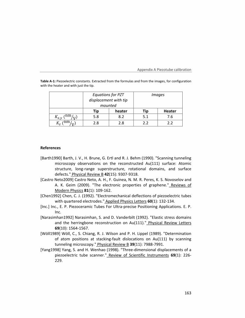
Appendix A Piezotube calibration
163
Table A-1: Piezoelectric constants. Extracted from the formulas and from the images, for configuration with the heater and with just the tip.
Equations for PZT
displacement with tip
mounted
Images
Tip heater Tip Heater ��,Á(nm V� ) 5.8 8.2 5.1 7.6
�À(nm V� ) 2.8 2.8 2.2 2.2
References
[Barth1990] Barth, J. V., H. Brune, G. Ertl and R. J. Behm (1990). "Scanning tunneling microscopy observations on the reconstructed Au(111) surface: Atomic structure, long-range superstructure, rotational domains, and surface defects." Physical Review B 42(15): 9307-9318.
[Castro Neto2009] Castro Neto, A. H., F. Guinea, N. M. R. Peres, K. S. Novoselov and A. K. Geim (2009). "The electronic properties of graphene." Reviews of Modern Physics 81(1): 109-162.
[Chen1992] Chen, C. J. (1992). "Electromechanical deflections of piezoelectric tubes with quartered electrodes." Applied Physics Letters 60(1): 132-134.
[Inc.] Inc., E. P. Piezoceramic Tubes For Ultra-precise Positioning Applications. E. P. Inc.
[Narasimhan1992] Narasimhan, S. and D. Vanderbilt (1992). "Elastic stress domains and the herringbone reconstruction on Au(111)." Physical Review Letters 69(10): 1564-1567.
[Wöll1989] Wöll, C., S. Chiang, R. J. Wilson and P. H. Lippel (1989). "Determination of atom positions at stacking-fault dislocations on Au(111) by scanning tunneling microscopy." Physical Review B 39(11): 7988-7991.
[Yang1998] Yang, S. and H. Wenhao (1998). "Three-dimensional displacements of a piezoelectric tube scanner." Review of Scientific Instruments 69(1): 226-229.
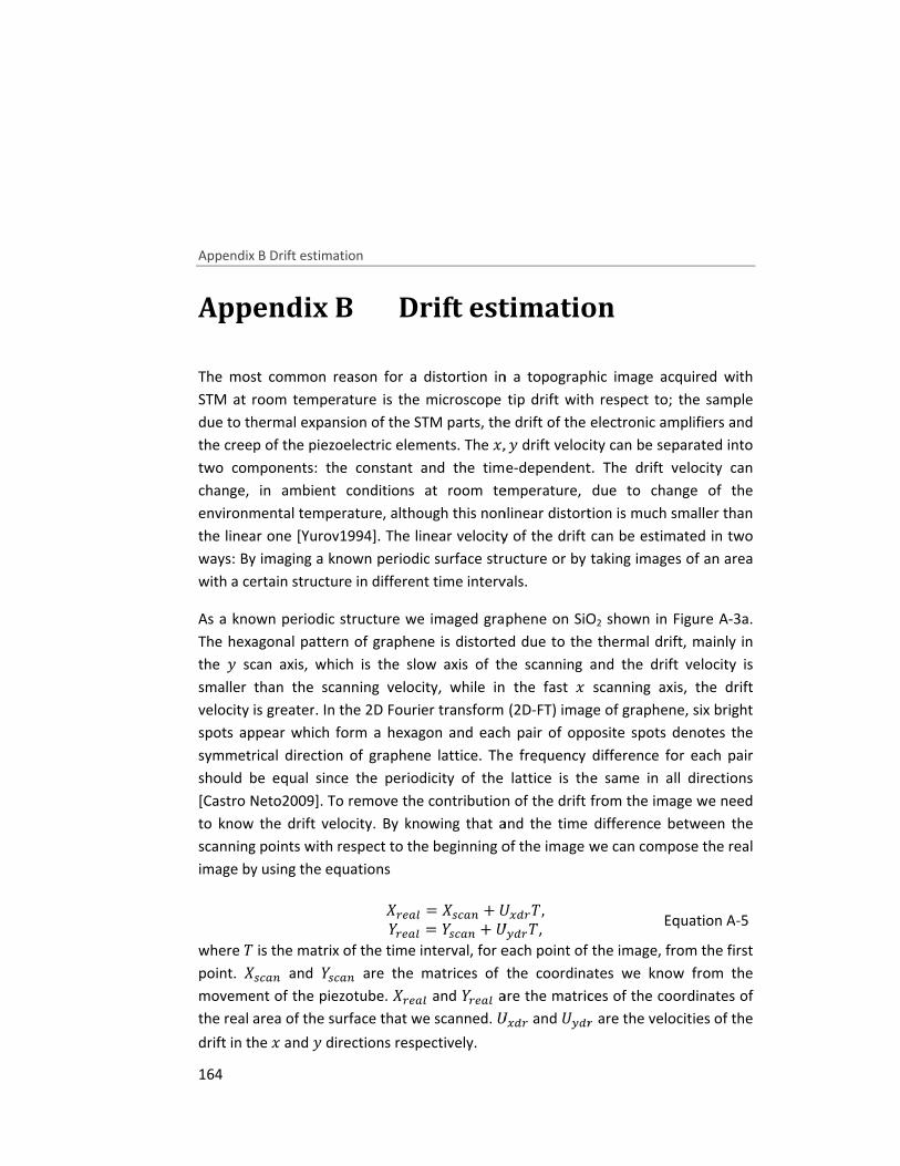
Appendix B
164
Appendix B
The most common reason for a distortion in a topographic image acquired with
STM at room temperature is the microscope tip drift with respect to
due to thermal expansion of the STM parts, the drift of the electronic amplifiers and
the creep of the piezoelectric elements. The
two components: the constant and the time
change, in ambient conditions at room temperature, due to change of the
environmental temperature, although this nonlinear distortion is
the linear one
ways: By imaging a known periodic surface structure or by taking images of an area
with a cert
As a known periodic structure we
The hexagonal pattern of graphene is distorted due to the thermal drift, mainly in
the ¾ scan axis, which is the slow axis of the scanning and the drift velocity is
smaller than the scanning velocity, while
velocity is greater
spots ap
symmetrical direction of graphene lattice. The frequency difference for each pair
should be equal since the periodicity of the lattice is the same in all directions
[Castro Neto2009
to know the drift velocity. By knowing that and the time difference between the
scanning points with respect to the beginning of the image we can compose the real
image by using the equations
where �point. ßmovement of the piezotube.
the real area of the surface that we scanned.
drift in the
Appendix B Drift estimation
Appendix B
The most common reason for a distortion in a topographic image acquired with
room temperature is the microscope tip drift with respect to
due to thermal expansion of the STM parts, the drift of the electronic amplifiers and
the creep of the piezoelectric elements. The
two components: the constant and the time
change, in ambient conditions at room temperature, due to change of the
environmental temperature, although this nonlinear distortion is
the linear one [Yurov1994
ways: By imaging a known periodic surface structure or by taking images of an area
with a certain structure in different time intervals.
As a known periodic structure we
The hexagonal pattern of graphene is distorted due to the thermal drift, mainly in
scan axis, which is the slow axis of the scanning and the drift velocity is
smaller than the scanning velocity, while
velocity is greater. In the 2D Fourier transform (2D
spots appear which form a hexagon and each pair of opposite spots denotes the
symmetrical direction of graphene lattice. The frequency difference for each pair
should be equal since the periodicity of the lattice is the same in all directions
Castro Neto2009]. To remove the contribution of the drift from the image we need
to know the drift velocity. By knowing that and the time difference between the
scanning points with respect to the beginning of the image we can compose the real
by using the equations
� is the matrix of the time interval, for each point of the image, from the first ß�Ç�A and à�Ç�Amovement of the piezotube.
the real area of the surface that we scanned.
drift in the 1 and ¾ directions respectively.
Drift estimation
Drift Appendix B
The most common reason for a distortion in a topographic image acquired with
room temperature is the microscope tip drift with respect to
due to thermal expansion of the STM parts, the drift of the electronic amplifiers and
the creep of the piezoelectric elements. The
two components: the constant and the time
change, in ambient conditions at room temperature, due to change of the
environmental temperature, although this nonlinear distortion is
Yurov1994]. The linear velocity of the drift can be estimated in two
ways: By imaging a known periodic surface structure or by taking images of an area
ain structure in different time intervals.
As a known periodic structure we
The hexagonal pattern of graphene is distorted due to the thermal drift, mainly in
scan axis, which is the slow axis of the scanning and the drift velocity is
smaller than the scanning velocity, while
. In the 2D Fourier transform (2D
pear which form a hexagon and each pair of opposite spots denotes the
symmetrical direction of graphene lattice. The frequency difference for each pair
should be equal since the periodicity of the lattice is the same in all directions
. To remove the contribution of the drift from the image we need
to know the drift velocity. By knowing that and the time difference between the
scanning points with respect to the beginning of the image we can compose the real
by using the equations
is the matrix of the time interval, for each point of the image, from the first
��A are the matrices of the coordinates we know from the
movement of the piezotube. ßxv�=the real area of the surface that we scanned.
directions respectively.
ßxv�=àxv�=
Drift estimation
The most common reason for a distortion in a topographic image acquired with
room temperature is the microscope tip drift with respect to
due to thermal expansion of the STM parts, the drift of the electronic amplifiers and
the creep of the piezoelectric elements. The 1,two components: the constant and the time
change, in ambient conditions at room temperature, due to change of the
environmental temperature, although this nonlinear distortion is
. The linear velocity of the drift can be estimated in two
ways: By imaging a known periodic surface structure or by taking images of an area
ain structure in different time intervals.
As a known periodic structure we imaged graphene on SiO
The hexagonal pattern of graphene is distorted due to the thermal drift, mainly in
scan axis, which is the slow axis of the scanning and the drift velocity is
smaller than the scanning velocity, while in the fast
. In the 2D Fourier transform (2D
pear which form a hexagon and each pair of opposite spots denotes the
symmetrical direction of graphene lattice. The frequency difference for each pair
should be equal since the periodicity of the lattice is the same in all directions
. To remove the contribution of the drift from the image we need
to know the drift velocity. By knowing that and the time difference between the
scanning points with respect to the beginning of the image we can compose the real
is the matrix of the time interval, for each point of the image, from the first
are the matrices of the coordinates we know from the
xv�= and àxv�= are the matrices of the coordinates of
the real area of the surface that we scanned. ádirections respectively.
� ß�Ç�A 9 á� à�Ç�A 9 á
stimation
The most common reason for a distortion in a topographic image acquired with
room temperature is the microscope tip drift with respect to
due to thermal expansion of the STM parts, the drift of the electronic amplifiers and , ¾ drift velocity can be
two components: the constant and the time-dependent
change, in ambient conditions at room temperature, due to change of the
environmental temperature, although this nonlinear distortion is
. The linear velocity of the drift can be estimated in two
ways: By imaging a known periodic surface structure or by taking images of an area
ain structure in different time intervals.
graphene on SiO
The hexagonal pattern of graphene is distorted due to the thermal drift, mainly in
scan axis, which is the slow axis of the scanning and the drift velocity is
in the fast 1
. In the 2D Fourier transform (2D-FT) image of graphene
pear which form a hexagon and each pair of opposite spots denotes the
symmetrical direction of graphene lattice. The frequency difference for each pair
should be equal since the periodicity of the lattice is the same in all directions
. To remove the contribution of the drift from the image we need
to know the drift velocity. By knowing that and the time difference between the
scanning points with respect to the beginning of the image we can compose the real
is the matrix of the time interval, for each point of the image, from the first
are the matrices of the coordinates we know from the
are the matrices of the coordinates of á�ax and áÁax
á�ax�, áÁax�,
stimation
The most common reason for a distortion in a topographic image acquired with
room temperature is the microscope tip drift with respect to;
due to thermal expansion of the STM parts, the drift of the electronic amplifiers and
drift velocity can be separated
dependent. The drift velocity can
change, in ambient conditions at room temperature, due to change of the
environmental temperature, although this nonlinear distortion is much smaller than
. The linear velocity of the drift can be estimated in two
ways: By imaging a known periodic surface structure or by taking images of an area
graphene on SiO2 shown in Figure A
The hexagonal pattern of graphene is distorted due to the thermal drift, mainly in
scan axis, which is the slow axis of the scanning and the drift velocity is
scanning axis
FT) image of graphene
pear which form a hexagon and each pair of opposite spots denotes the
symmetrical direction of graphene lattice. The frequency difference for each pair
should be equal since the periodicity of the lattice is the same in all directions
. To remove the contribution of the drift from the image we need
to know the drift velocity. By knowing that and the time difference between the
scanning points with respect to the beginning of the image we can compose the real
is the matrix of the time interval, for each point of the image, from the first
are the matrices of the coordinates we know from the
are the matrices of the coordinates of
Áax are the velocit
Equation A
The most common reason for a distortion in a topographic image acquired with
the sample
due to thermal expansion of the STM parts, the drift of the electronic amplifiers and
separated into
. The drift velocity can
change, in ambient conditions at room temperature, due to change of the
much smaller than
. The linear velocity of the drift can be estimated in two
ways: By imaging a known periodic surface structure or by taking images of an area
Figure A-3a.
The hexagonal pattern of graphene is distorted due to the thermal drift, mainly in
scan axis, which is the slow axis of the scanning and the drift velocity is
scanning axis, the drift
FT) image of graphene, six bright
pear which form a hexagon and each pair of opposite spots denotes the
symmetrical direction of graphene lattice. The frequency difference for each pair
should be equal since the periodicity of the lattice is the same in all directions
. To remove the contribution of the drift from the image we need
to know the drift velocity. By knowing that and the time difference between the
scanning points with respect to the beginning of the image we can compose the real
is the matrix of the time interval, for each point of the image, from the first
are the matrices of the coordinates we know from the
are the matrices of the coordinates of
he velocities of the
Equation A-5
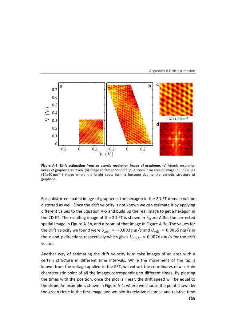
Appendix B Drift estimation
165
Figure A-3: Drift estimation from an atomic resolution image of graphene. (a) Atomic resolution image of graphene as taken. (b) Image corrected for drift. (c) A zoom in an area of image (b). (d) 2D-FT (40x40nm�') image where the bright spots form a hexagon due to the periodic structure of graphene.
For a distorted spatial image of graphene, the hexagon in the 2D-FT domain will be
distorted as well. Since the drift velocity is not known we can estimate it by applying
different values to the Equation A-5 and build up the real image to get a hexagon in
the 2D-FT. The resulting image of the 2D-FT is shown in Figure A-3d, the corrected
spatial image in Figure A-3b, and a zoom of that image in Figure A-3c. The values for
the drift velocity we found were á�ax = −0.003 nm Y⁄ and áÁax = 0.0065 nm s⁄ in
the 1 and ¾ directions respectively which gives áax�wm ≈ 0.0076 ?$ Y⁄ for the drift
vector.
Another way of estimating the drift velocity is to take images of an area with a
certain structure in different time intervals. While the movement of the tip is
known from the voltage applied to the PZT, we extract the coordinates of a certain
characteristic point of all the images corresponding to different times. By plotting
the times with the position, once the plot is linear, the drift speed will be equal to
the slope. An example is shown in Figure A-4, where we choose the point shown by
the green circle in the first image and we plot its relative distance and relative time
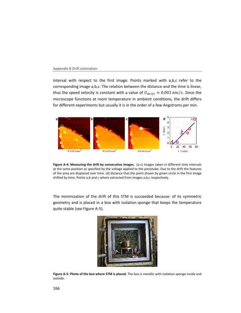
Appendix B Drift estimation
166
interval with respect to the first image. Points marked with a,b,c refer to the
corresponding image a,b,c. The relation between the distance and the time is linear,
thus the speed velocity is constant with a value of áax�wm ≈ 0.001 ?$ Y⁄ . Since the
microscope functions at room temperature in ambient conditions, the drift differs
for different experiments but usually it is in the order of a few Angstroms per min.
Figure A-4: Measuring the drift by consecutive images. (a-c) Images taken in different time intervals at the same position as specified by the voltage applied to the piezotube. Due to the drift the features of the area are displaced over time. (d) distance that the point shown by green circle in the first image shifted by time. Points a,b and c where extracted from images a,b,c respectively.
The minimization of the drift of this STM is succeeded because: of its symmetric
geometry and is placed in a box with isolation sponge that keeps the temperature
quite stable (see Figure A-5).
Figure A-5: Photo of the box where STM is placed. The box is metallic with isolation sponge inside and outside.
Appendix B Drift estimation
167
References
[Castro Neto2009] Castro Neto, A. H., F. Guinea, N. M. R. Peres, K. S. Novoselov and A. K. Geim (2009). "The electronic properties of graphene." Reviews of Modern Physics 81(1): 109-162.
[Yurov1994] Yurov, V. Y. and A. N. Klimov (1994). "Scanning tunneling microscope calibration and reconstruction of real image: Drift and slope elimination." Review of Scientific Instruments 65(5): 1551-1557.
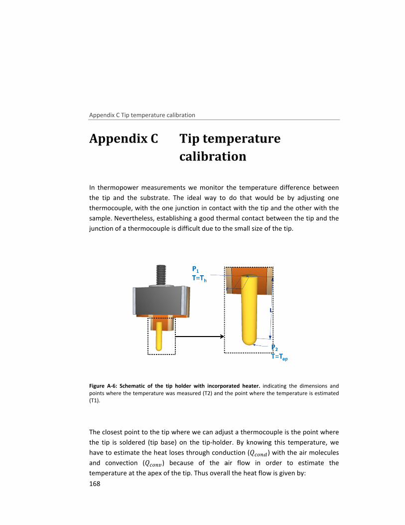
Appendix C
168
Appendix C
In thermopower measurements we monitor the temperature differe
the tip and the substrate. The ideal way to do that would be by adjusting one
thermocouple, with the one junction in contact with the tip and the other with the
sample. Nevertheless
junction of a thermocouple is difficult due to the small size of the tip.
Figure A-6
points where the temperature was measured (T2) and (T1).
The closest point to the tip where we can adjust a thermocouple is the point where
the tip is soldered (tip base) on the tip
have to estimate the heat loses through
and convection (
temperature at the apex of the tip
Appendix C Tip temperature calibration
Appendix C
In thermopower measurements we monitor the temperature differe
the tip and the substrate. The ideal way to do that would be by adjusting one
thermocouple, with the one junction in contact with the tip and the other with the
sample. Nevertheless
unction of a thermocouple is difficult due to the small size of the tip.
6: Schematic of the tip
points where the temperature was measured (T2) and
The closest point to the tip where we can adjust a thermocouple is the point where
the tip is soldered (tip base) on the tip
have to estimate the heat loses through
and convection (rÇÉA�temperature at the apex of the tip
Tip temperature calibration
Tip temperature Appendix C
calibration
In thermopower measurements we monitor the temperature differe
the tip and the substrate. The ideal way to do that would be by adjusting one
thermocouple, with the one junction in contact with the tip and the other with the
sample. Nevertheless, establishing a good thermal contact between the tip and the
unction of a thermocouple is difficult due to the small size of the tip.
Schematic of the tip holder with incorporated heater.
points where the temperature was measured (T2) and
The closest point to the tip where we can adjust a thermocouple is the point where
the tip is soldered (tip base) on the tip
have to estimate the heat loses through
ÇÉA�) because of the air flow
temperature at the apex of the tip
Tip temperature calibration
Tip temperature
calibration
In thermopower measurements we monitor the temperature differe
the tip and the substrate. The ideal way to do that would be by adjusting one
thermocouple, with the one junction in contact with the tip and the other with the
establishing a good thermal contact between the tip and the
unction of a thermocouple is difficult due to the small size of the tip.
holder with incorporated heater.
points where the temperature was measured (T2) and the
The closest point to the tip where we can adjust a thermocouple is the point where
the tip is soldered (tip base) on the tip-holder. By knowing this temperature,
have to estimate the heat loses through conduction
because of the air flow
temperature at the apex of the tip. Thus overall the
Tip temperature
calibration
In thermopower measurements we monitor the temperature differe
the tip and the substrate. The ideal way to do that would be by adjusting one
thermocouple, with the one junction in contact with the tip and the other with the
establishing a good thermal contact between the tip and the
unction of a thermocouple is difficult due to the small size of the tip.
holder with incorporated heater. indicating the dimensions and the point where the temperature is estimated
The closest point to the tip where we can adjust a thermocouple is the point where
holder. By knowing this temperature,
nduction (rÇÉAabecause of the air flow in order to estimate the
Thus overall the heat flow
Tip temperature
In thermopower measurements we monitor the temperature difference between
the tip and the substrate. The ideal way to do that would be by adjusting one
thermocouple, with the one junction in contact with the tip and the other with the
establishing a good thermal contact between the tip and the
unction of a thermocouple is difficult due to the small size of the tip.
indicating the dimensions and point where the temperature is estimated
The closest point to the tip where we can adjust a thermocouple is the point where
holder. By knowing this temperature,
ÇÉAa) with the air molecules
in order to estimate the
heat flow is given by
nce between
the tip and the substrate. The ideal way to do that would be by adjusting one
thermocouple, with the one junction in contact with the tip and the other with the
establishing a good thermal contact between the tip and the
indicating the dimensions and point where the temperature is estimated
The closest point to the tip where we can adjust a thermocouple is the point where
holder. By knowing this temperature, we
with the air molecules
in order to estimate the
by:
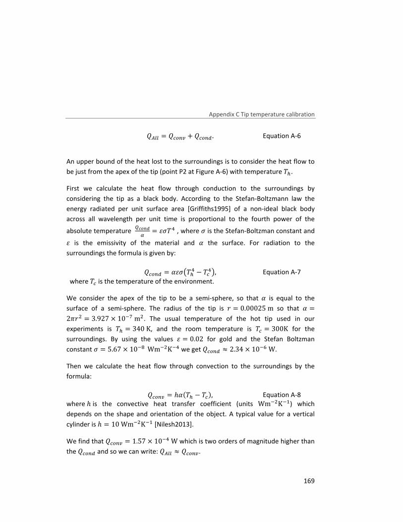
Appendix C Tip temperature calibration
169
An upper bound of the heat lost to the surroundings is to consider the heat flow to
be just from the apex of the tip (point P2 at Figure A-6) with temperature �n.
First we calculate the heat flow through conduction to the surroundings by
considering the tip as a black body. According to the Stefan-Boltzmann law the
energy radiated per unit surface area [Griffiths1995] of a non-ideal black body
across all wavelength per unit time is proportional to the fourth power of the
absolute temperature ãäåæçc = e��Ó , where � is the Stefan-Boltzman constant and e is the emissivity of the material and � the surface. For radiation to the
surroundings the formula is given by:
where �Ç is the temperature of the environment.
We consider the apex of the tip to be a semi-sphere, so that � is equal to the
surface of a semi-sphere. The radius of the tip is � = 0.00025m so that � =2|�� = 3.927 × 10�Ìm�. The usual temperature of the hot tip used in our
experiments is �n = 340K, and the room temperature is �Ç = 300K for the
surroundings. By using the values e = 0.02 for gold and the Stefan Boltzman
constant � = 5.67 × 10�¢Wm��K�Ó we get rÇÉAa ≈ 2.34 × 10�ÎW.
Then we calculate the heat flow through convection to the surroundings by the
formula:
where ℎ is the convective heat transfer coefficient (units Wm��K�') which
depends on the shape and orientation of the object. A typical value for a vertical
cylinder is ℎ = 10Wm��K�' [Nilesh2013].
We find that rÇÉA� = 1.57 × 10�ÓW which is two orders of magnitude higher than
the rÇÉAa and so we can write: rp== ≈ rÇÉA�.
rp== = rÇÉA� + rÇÉAa . Equation A-6
rÇÉAa = �e���nÓ − �ÇÓ�, Equation A-7
rÇÉA� = ℎ�(�n − �Ç), Equation A-8
Appendix C Tip temperature calibration
170
In order to calculate the temperature at the apex of the tip we use the formula for
heat conduction within a material [Datta2005]:
where k is the thermal conductivity, `is the surface area of the tip, � the thickness
and �� the difference of temperature between the tip base and the apex, �Ç − ���.
By using the parameters ` = 2|�� = 6.042 × 10�Îm�, � = 0.00025m,
� = 0.004m," = 317W mK� for the gold tip we get that �� = 3.3 × 10�ÒK
which is very small and practically means that the apex of the tip has the same
temperature with the tip base.
In addition to this small drop of temperature, another drop is expected to appear
when the tip is closed to the sample, which is kept in room temperature �Ç, due to
heat transport because of conduction through air and conduction through the
organic molecules which may be bridging the gap between the substrate and the
tip. It has been calculated by Reddy et al [Reddy2007] that even when the tip-
substrate gap is reduced to 1nm, the temperature at the very end of the tip will be
��� ≈ �n − 0.01(�n − �Ç), which is less than one percent of the temperature
differential applied across the substrate and tip.
During the experiments we monitor the temperature difference between the
heater (resistor) and the substrate. Then, while the temperature at the tip base and
at the apex of the tip is the same, we just need to estimate the temperature drop
between the resistor and tip base. To calibrate that, we used three type-k chromel -
alumel thermocouples. The one junction of every thermocouple was always placed
on the body of the microscope and the other on the tip holder, the heater and the
sample, respectively. With the one on the sample we check the effect of the heat
radiated from the heater to the gold sample. Then by increasing the temperature of
the heater and keeping the tip in tunneling with the sample we measure the
temperature of the different points mentioned above. In Figure A-7a,b the points
where the thermocouples were adjusted are indicated by arrows.
rp== = "� (��) ≈ rÇÉA� , Equation A-9
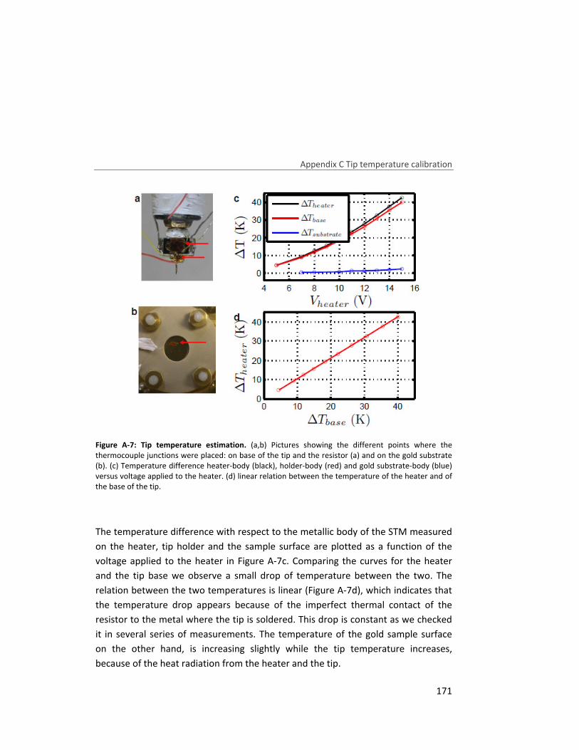
Appendix C Tip temperature calibration
171
Figure A-7: Tip temperature estimation. (a,b) Pictures showing the different points where the thermocouple junctions were placed: on base of the tip and the resistor (a) and on the gold substrate (b). (c) Temperature difference heater-body (black), holder-body (red) and gold substrate-body (blue) versus voltage applied to the heater. (d) linear relation between the temperature of the heater and of the base of the tip.
The temperature difference with respect to the metallic body of the STM measured
on the heater, tip holder and the sample surface are plotted as a function of the
voltage applied to the heater in Figure A-7c. Comparing the curves for the heater
and the tip base we observe a small drop of temperature between the two. The
relation between the two temperatures is linear (Figure A-7d), which indicates that
the temperature drop appears because of the imperfect thermal contact of the
resistor to the metal where the tip is soldered. This drop is constant as we checked
it in several series of measurements. The temperature of the gold sample surface
on the other hand, is increasing slightly while the tip temperature increases,
because of the heat radiation from the heater and the tip.

Appendix C Tip temperature calibration
172
Finally, we checked how the temperature of the tip varies if it is in tunneling or in
contact with the sample. For junctions with conductance of the order of ~100�
no changes where observed. A small drop of the temperature of the order of 2%
was observed by creating macroscopic metallic junctions using the coarse
movement of the tip.
Consequently, in this thesis, when the temperature difference was measured
between the heater and the sample we discounted the loss of heat due to the
thermal contact of the resistor to the metal where the tip is soldered.
References
[Datta2005] Datta, S. (2005). Quantum Transport: Atom to Transistor, Cambridge University Press.
[Griffiths1995] Griffiths, D. J. (1995). Introduction to Quantum Mechanics, Prentice Hall.
[Nilesh2013] Nilesh, M., Nanasaheb, Vijay and S. Totala, Shete,Bhopate (2013). "Natural Convection Characteristicsin Vertical Cylinder." International Journal Of Engineering And Science 3(8): 27-31.
[Reddy2007] Reddy, P., S.-Y. Jang, R. A. Segalman and A. Majumdar (2007). "Thermoelectricity in Molecular Junctions." Science 315(5818): 1568-1571.
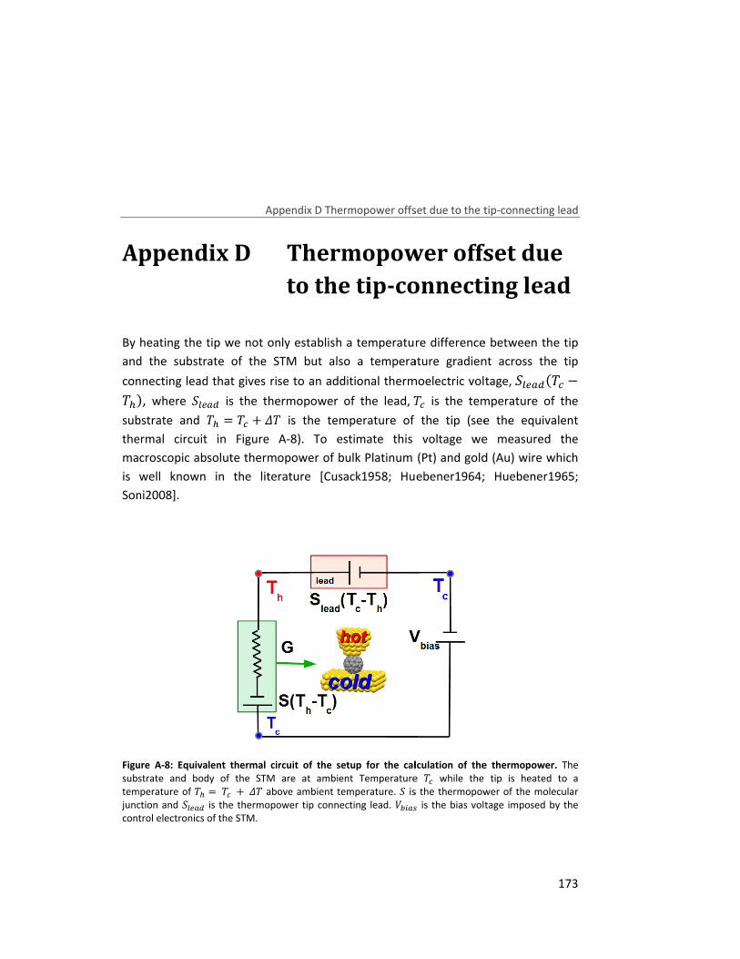
Appendix D
By heating
and the substrate of the STM but also a temperature gradient across
connecting �n)substrate and
thermal circuit in
macroscopic absolute thermopower of bulk Platinum (Pt) and gold (Au)
is well known in the literature
Soni2008
Figure A
substrate and body of the STM are at ambient Temperature temperature of junction and control electronics of the STM.
Appendix D
By heating the tip we not only establish a temperature difference between the tip
and the substrate of the STM but also a temperature gradient across
connecting lead ), where �=v�asubstrate and �thermal circuit in
macroscopic absolute thermopower of bulk Platinum (Pt) and gold (Au)
is well known in the literature
Soni2008].
Figure A-8: Equivalent thermal circui
substrate and body of the STM are at ambient Temperature temperature of �njunction and �=v�a control electronics of the STM.
Appendix D
Appendix D
the tip we not only establish a temperature difference between the tip
and the substrate of the STM but also a temperature gradient across
lead that gives rise to an additional thermoelectric voltage
=v�a is the thermopower �n = �Ç + ��thermal circuit in Figure A
macroscopic absolute thermopower of bulk Platinum (Pt) and gold (Au)
is well known in the literature
: Equivalent thermal circui
substrate and body of the STM are at ambient Temperature =�Ç + �� above ambient temperature. is the thermopower
control electronics of the STM.
Appendix D Thermopower offset due to the tip
Thermopower offset due
to the tip
the tip we not only establish a temperature difference between the tip
and the substrate of the STM but also a temperature gradient across
that gives rise to an additional thermoelectric voltage
is the thermopower of � is the temperature of the tip (see the equivalent
Figure A-8). To estimate this
macroscopic absolute thermopower of bulk Platinum (Pt) and gold (Au)
is well known in the literature [Cusack1958
: Equivalent thermal circuit of the setup for the calculation of the thermopower.
substrate and body of the STM are at ambient Temperature above ambient temperature.
is the thermopower tip connecting lead
Thermopower offset due to the tip
Thermopower offset due
to the tip-connecting lead
the tip we not only establish a temperature difference between the tip
and the substrate of the STM but also a temperature gradient across
that gives rise to an additional thermoelectric voltage
of the lead,�is the temperature of the tip (see the equivalent
o estimate this
macroscopic absolute thermopower of bulk Platinum (Pt) and gold (Au)
Cusack1958; Huebener1964
t of the setup for the calculation of the thermopower.
substrate and body of the STM are at ambient Temperature above ambient temperature. � is the thermopower of the molecula
tip connecting lead. ����
Thermopower offset due to the tip
Thermopower offset due
connecting lead
the tip we not only establish a temperature difference between the tip
and the substrate of the STM but also a temperature gradient across
that gives rise to an additional thermoelectric voltage�Ç is the temperature of the
is the temperature of the tip (see the equivalent
o estimate this voltage we measured the
macroscopic absolute thermopower of bulk Platinum (Pt) and gold (Au)
Huebener1964;
t of the setup for the calculation of the thermopower.
substrate and body of the STM are at ambient Temperature �Ç while the tip is heated to a is the thermopower of the molecula
��� is the bias voltage imposed by the
Thermopower offset due to the tip-connecting
Thermopower offset due
connecting lead
the tip we not only establish a temperature difference between the tip
and the substrate of the STM but also a temperature gradient across the tip
that gives rise to an additional thermoelectric voltage,�=v�a(�is the temperature of the
is the temperature of the tip (see the equivalent
voltage we measured the
macroscopic absolute thermopower of bulk Platinum (Pt) and gold (Au) wire which
; Huebener1965
t of the setup for the calculation of the thermopower.
while the tip is heated to a is the thermopower of the molecula
is the bias voltage imposed by the
connecting lead
173
Thermopower offset due
connecting lead
the tip we not only establish a temperature difference between the tip
the tip (�Ç −is the temperature of the
is the temperature of the tip (see the equivalent
voltage we measured the
which
Huebener1965;
t of the setup for the calculation of the thermopower. The while the tip is heated to a
is the thermopower of the molecular is the bias voltage imposed by the
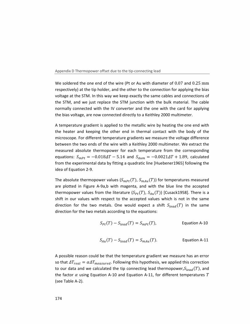
Appendix D Thermopower offset due to the tip-connecting lead
174
We soldered the one end of the wire (Pt or Au with diameter of 0.07 and 0.25mm
respectively) at the tip holder, and the other to the connection for applying the bias
voltage at the STM. In this way we keep exactly the same cables and connections of
the STM, and we just replace the STM junction with the bulk material. The cable
normally connected with the IV converter and the one with the card for applying
the bias voltage, are now connected directly to a Keithley 2000 multimeter.
A temperature gradient is applied to the metallic wire by heating the one end with
the heater and keeping the other end in thermal contact with the body of the
microscope. For different temperature gradients we measure the voltage difference
between the two ends of the wire with a Keithley 2000 multimeter. We extract the
measured absolute thermopower for each temperature from the corresponding
equations: �Pèm = −0.018�� − 5.14 and �p�P = −0.0021�� + 1.89, calculated
from the experimental data by fitting a quadratic line [Huebener1965] following the
idea of Equation 2-9.
The absolute thermopower values (�Pèm(�), �Pp�(�)) for temperatures measured
are plotted in Figure A-9a,b with magenta, and with the blue line the accepted
thermopower values from the literature (�èm(�), �p�(�)) [Cusack1958]. There is a
shift in our values with respect to the accepted values which is not in the same
direction for the two metals. One would expect a shift �=v�a(�) in the same
direction for the two metals according to the equations:
A possible reason could be that the temperature gradient we measure has an error
so that ��xv�= = ���Pv���xva. Following this hypothesis, we applied this correction
to our data and we calculated the tip connecting lead thermopower,�=v�a(�), and
the factor � using Equation A-10 and Equation A-11, for different temperatures �
(see Table A-2).
�èm(�) − �=v�a(�) = �Pèm(�), Equation A-10
�p�(�) − �=v�a(�) = �Pp�(�). Equation A-11
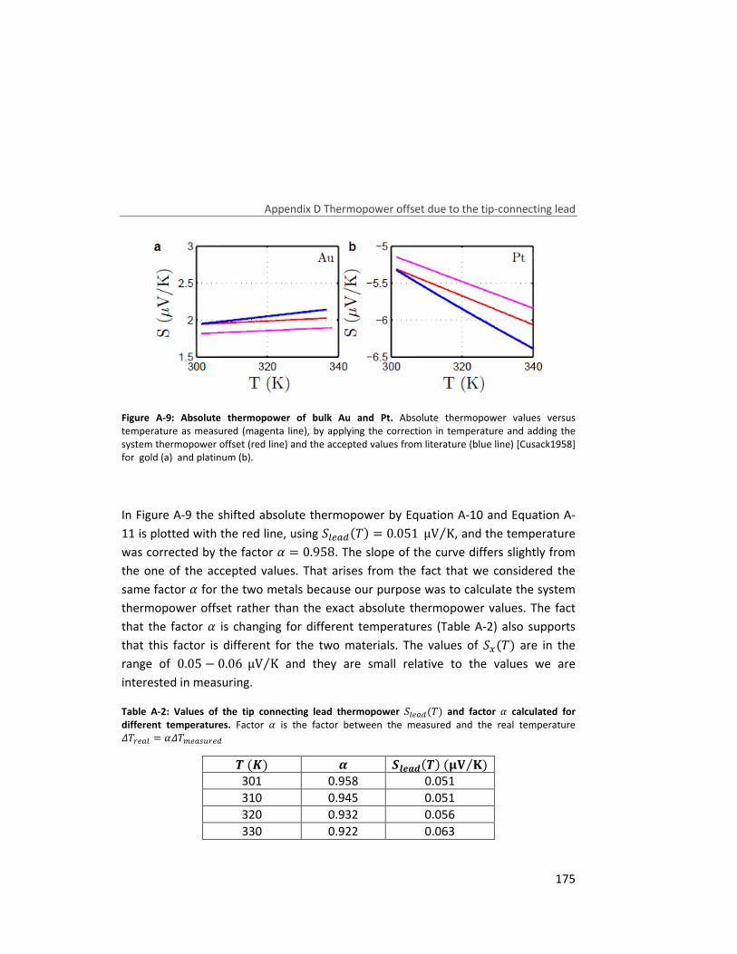
Appendix D Thermopower offset due to the tip-connecting lead
175
Figure A-9: Absolute thermopower of bulk Au and Pt. Absolute thermopower values versus temperature as measured (magenta line), by applying the correction in temperature and adding the system thermopower offset (red line) and the accepted values from literature (blue line) [Cusack1958] for gold (a) and platinum (b).
In Figure A-9 the shifted absolute thermopower by Equation A-10 and Equation A-
11 is plotted with the red line, using �=v�a(�) = 0.051 μV K⁄ , and the temperature
was corrected by the factor � = 0.958. The slope of the curve differs slightly from
the one of the accepted values. That arises from the fact that we considered the
same factor � for the two metals because our purpose was to calculate the system
thermopower offset rather than the exact absolute thermopower values. The fact
that the factor � is changing for different temperatures (Table A-2) also supports
that this factor is different for the two materials. The values of ��(�) are in the
range of 0.05 − 0.06 μV K⁄ and they are small relative to the values we are
interested in measuring.
Table A-2: Values of the tip connecting lead thermopower �=v�a(�) and factor � calculated for
different temperatures. Factor � is the factor between the measured and the real temperature ��xv�= = ���Pv���xva
é(ê) ë �ìíîï(é)(�� �⁄ ) 301 0.958 0.051 310 0.945 0.051 320 0.932 0.056 330 0.922 0.063
Appendix D Thermopower offset due to the tip-connecting lead
176
References
[Cusack1958] Cusack, N. and P. Kendall (1958). "The Absolute Scale of Thermoelectric Power at High Temperature." Proceedings of the Physical Society (1960) 72(5): 898-901.
[Huebener1964] Huebener, R. P. (1964). "THERMOELECTRIC POWER OF LATTICE VACANCIES IN GOLD." PHYSICAL REVIEW A-GENERAL PHYSICS 135(5a): 1281-&.
[Huebener1965] Huebener, R. P. (1965). "SIZE EFFECT ON PHONON DRAG IN PLATINUM." Physical review 140(5a): 1834-&.
[Soni2008] Soni, A. and G. S. Okram (2008). "Resistivity and thermopower measurement setups in the temperature range of 5–325 K." Review of Scientific Instruments 79(12): -.
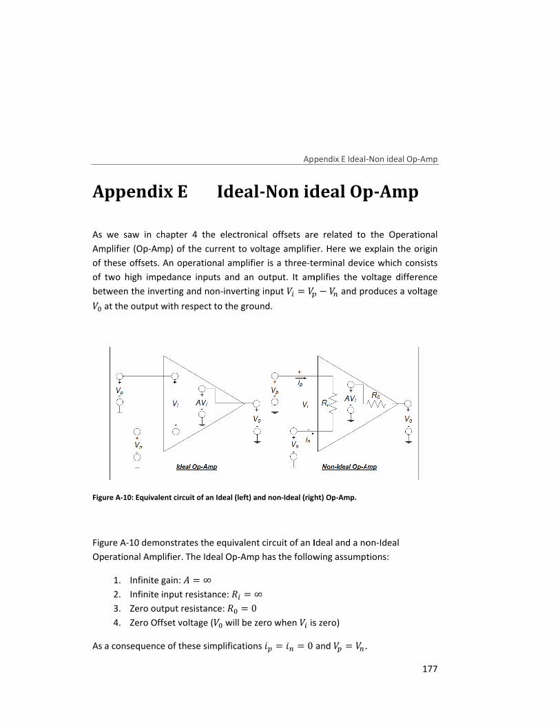
Appendix E
As we saw in chapter
Amplifier (Op
of these offsets.
of two high impedance inputs and an output. It amplifies the voltage difference
between the inverting and non� at the output with
Figure A
Figure A
Operational Amplifier. The Ideal Op
As a consequence of these simplifications
Appendix E
As we saw in chapter
Amplifier (Op-Amp) of the current to voltage amplifier.
of these offsets.
of two high impedance inputs and an output. It amplifies the voltage difference
between the inverting and non
at the output with
Figure A-10: Equivalent circuit of an Ideal (left) and non
Figure A-10 demonstrates the equivalent circuit of an Ideal and a non
Operational Amplifier. The Ideal Op
1. Infinite gain:
2. Infinite input resistance:
3. Zero output resistance:
4. Zero Offset voltage (
As a consequence of these simplifications
Appendix E
As we saw in chapter 4 the electronical offsets are related to the Operational
Amp) of the current to voltage amplifier.
of these offsets. An operational amplifier is a three
of two high impedance inputs and an output. It amplifies the voltage difference
between the inverting and non
at the output with respect to the ground.
Equivalent circuit of an Ideal (left) and non
demonstrates the equivalent circuit of an Ideal and a non
Operational Amplifier. The Ideal Op
Infinite gain: ` = ∞Infinite input resistance:
Zero output resistance:
Zero Offset voltage (
As a consequence of these simplifications
Ideal-
the electronical offsets are related to the Operational
Amp) of the current to voltage amplifier.
operational amplifier is a three
of two high impedance inputs and an output. It amplifies the voltage difference
between the inverting and non-inverting input
respect to the ground.
Equivalent circuit of an Ideal (left) and non
demonstrates the equivalent circuit of an Ideal and a non
Operational Amplifier. The Ideal Op-Amp has the followin
∞
Infinite input resistance: �� = ∞Zero output resistance: � = 0
Zero Offset voltage (� will be zero when
As a consequence of these simplifications
Appendix E
-Non ideal Op
the electronical offsets are related to the Operational
Amp) of the current to voltage amplifier.
operational amplifier is a three-terminal device
of two high impedance inputs and an output. It amplifies the voltage difference
inverting input �� = ��respect to the ground.
Equivalent circuit of an Ideal (left) and non-Ideal (right) Op
demonstrates the equivalent circuit of an Ideal and a non
Amp has the followin
∞
will be zero when �� is zero)
As a consequence of these simplifications -� = -A = 0
Appendix E Ideal-
Non ideal Op
the electronical offsets are related to the Operational
Amp) of the current to voltage amplifier. Here we explain the origin
terminal device
of two high impedance inputs and an output. It amplifies the voltage difference �� − �A and produces a voltage
Ideal (right) Op-Amp.
demonstrates the equivalent circuit of an Ideal and a non
Amp has the following assumptions:
is zero)
and �� = �A.
-Non ideal Op-
Non ideal Op-Amp
the electronical offsets are related to the Operational
Here we explain the origin
terminal device which consists
of two high impedance inputs and an output. It amplifies the voltage difference
and produces a voltage
demonstrates the equivalent circuit of an Ideal and a non-Ideal
g assumptions:
.
-Amp
177
the electronical offsets are related to the Operational
Here we explain the origin
which consists
of two high impedance inputs and an output. It amplifies the voltage difference
and produces a voltage
Appendix E Ideal-Non ideal Op-Amp
178
A non-ideal Op-Amp, which is normally the case, will have the following
characteristics.
1. Bias current (���): The average of the current of the 2 inputs of the Op-
Amp. It is caused by the transistors’ inputs (that are inside the Op-amp)
which draw some current.
2. Offset current (º�): The difference between the input bias currents. Each
current, by entering the Op-Amp, will finally give an offset voltage at the
output.
3. Input Offset Voltage(�º�): The voltage produced in the inputs of the Op-
Amp due to the DC imbalances within it.
4. Drift: A general term that describes the variation of the DC characteristics
of the Op-Amp by time and/or temperature.

Appendix F
The most common way of depositing C
evaporat
deposition techniques such
[Červenka2010
used drop casting. We deposit the molecules from dilute solutions in 1, 2, 4
trichlorobenzene (TCB) of concentrations clos
drops to a freshly flame
minutes, we bl
argon gas. Then we let the sample dry for several ho
images of such samples for different concentrations are shown in
Concentrations close to 10
molecules spread across terraces and steps, and some small islands of molecules.
Increasing the concentration around 10
bigger and we can still see some i5 M (
not many individual molecules can be fou
In some cases we used the dip casting technique where we dip the sample in the C
solution for several hours and then we dry it in the same way. In this way the
molecules have time
dipped in a solution in Dichloromethane (DCM) with concentration of 10
hours. Areas
disordered molecules.
molecules on the surface which sometimes were very mobile. It is important to
mention here that images
sharper images (see chapter
Appendix F
The most common way of depositing C
evaporation in
deposition techniques such
Červenka2010]
used drop casting. We deposit the molecules from dilute solutions in 1, 2, 4
trichlorobenzene (TCB) of concentrations clos
drops to a freshly flame
minutes, we blow
argon gas. Then we let the sample dry for several ho
images of such samples for different concentrations are shown in
Concentrations close to 10
molecules spread across terraces and steps, and some small islands of molecules.
Increasing the concentration around 10
bigger and we can still see some i
M (Figure A-11
not many individual molecules can be fou
In some cases we used the dip casting technique where we dip the sample in the C
solution for several hours and then we dry it in the same way. In this way the
molecules have time
dipped in a solution in Dichloromethane (DCM) with concentration of 10
hours. Areas of
disordered molecules.
molecules on the surface which sometimes were very mobile. It is important to
mention here that images
sharper images (see chapter
Appendix F
The most common way of depositing C
ultra-high vacuum
deposition techniques such
are also used
used drop casting. We deposit the molecules from dilute solutions in 1, 2, 4
trichlorobenzene (TCB) of concentrations clos
drops to a freshly flamed annealed gold (1,1,1) substrate. After waiting a couple of
ow off the excess solvent and dr
argon gas. Then we let the sample dry for several ho
images of such samples for different concentrations are shown in
Concentrations close to 10
molecules spread across terraces and steps, and some small islands of molecules.
Increasing the concentration around 10
bigger and we can still see some i
11g-i) and 10-
not many individual molecules can be fou
In some cases we used the dip casting technique where we dip the sample in the C
solution for several hours and then we dry it in the same way. In this way the
molecules have time to organize on the surface. In
dipped in a solution in Dichloromethane (DCM) with concentration of 10
of hexagonally closed pack structure can be found, as well as
disordered molecules. Imaging such samples was quite difficult
molecules on the surface which sometimes were very mobile. It is important to
mention here that images Figure A
sharper images (see chapter
C60 deposition
The most common way of depositing C
vacuum [Joachim1995
deposition techniques such as drop casting
also used, but less frequent
used drop casting. We deposit the molecules from dilute solutions in 1, 2, 4
trichlorobenzene (TCB) of concentrations clos
annealed gold (1,1,1) substrate. After waiting a couple of
off the excess solvent and dr
argon gas. Then we let the sample dry for several ho
images of such samples for different concentrations are shown in
Concentrations close to 10-8 M (Figure A
molecules spread across terraces and steps, and some small islands of molecules.
Increasing the concentration around 10-7
bigger and we can still see some individual molecules. For higher concentrations 106 M (Figure A
not many individual molecules can be fou
In some cases we used the dip casting technique where we dip the sample in the C
solution for several hours and then we dry it in the same way. In this way the
organize on the surface. In
dipped in a solution in Dichloromethane (DCM) with concentration of 10
hexagonally closed pack structure can be found, as well as
maging such samples was quite difficult
molecules on the surface which sometimes were very mobile. It is important to
Figure A-11e,f,k,l ware taken with a C
5).
eposition
The most common way of depositing C60 molecules on gold is by thermal
Joachim1995; Gardener2009
rop casting [Guo2004
less frequently. In our experiments we
used drop casting. We deposit the molecules from dilute solutions in 1, 2, 4
trichlorobenzene (TCB) of concentrations close to 10-
annealed gold (1,1,1) substrate. After waiting a couple of
off the excess solvent and dry the substrate under a stream of
argon gas. Then we let the sample dry for several ho
images of such samples for different concentrations are shown in
Figure A-11a-c) give samples w
molecules spread across terraces and steps, and some small islands of molecules.
M (Figure A-
ndividual molecules. For higher concentrations 10
Figure A-11j) the number of islands increase and
not many individual molecules can be found.
In some cases we used the dip casting technique where we dip the sample in the C
solution for several hours and then we dry it in the same way. In this way the
organize on the surface. In Figure A
dipped in a solution in Dichloromethane (DCM) with concentration of 10
hexagonally closed pack structure can be found, as well as
maging such samples was quite difficult
molecules on the surface which sometimes were very mobile. It is important to
e,f,k,l ware taken with a C
Appendix F
eposition
molecules on gold is by thermal
Gardener2009; S
Guo2004] and s
. In our experiments we
used drop casting. We deposit the molecules from dilute solutions in 1, 2, 4-5 - 10-8 M by applying several
annealed gold (1,1,1) substrate. After waiting a couple of
the substrate under a stream of
argon gas. Then we let the sample dry for several hours. Examples of topographic
images of such samples for different concentrations are shown in
c) give samples w
molecules spread across terraces and steps, and some small islands of molecules.
-11d-f) the islands are getting
ndividual molecules. For higher concentrations 10
j) the number of islands increase and
In some cases we used the dip casting technique where we dip the sample in the C
solution for several hours and then we dry it in the same way. In this way the
Figure A-11k,l the sample was
dipped in a solution in Dichloromethane (DCM) with concentration of 10
hexagonally closed pack structure can be found, as well as
maging such samples was quite difficult due to the many
molecules on the surface which sometimes were very mobile. It is important to
e,f,k,l ware taken with a C60
Appendix F C60 deposition
molecules on gold is by thermal
Schull2009]. Wet
and spray coating
. In our experiments we mainly
used drop casting. We deposit the molecules from dilute solutions in 1, 2, 4
M by applying several
annealed gold (1,1,1) substrate. After waiting a couple of
the substrate under a stream of
urs. Examples of topographic
images of such samples for different concentrations are shown in Figure A-11
c) give samples with individual
molecules spread across terraces and steps, and some small islands of molecules.
f) the islands are getting
ndividual molecules. For higher concentrations 10
j) the number of islands increase and
In some cases we used the dip casting technique where we dip the sample in the C
solution for several hours and then we dry it in the same way. In this way the
l the sample was
dipped in a solution in Dichloromethane (DCM) with concentration of 10-6 M for 24
hexagonally closed pack structure can be found, as well as
due to the many
molecules on the surface which sometimes were very mobile. It is important to
60 tip, which gives
C60 deposition
179
molecules on gold is by thermal
. Wet
pray coating
mainly
used drop casting. We deposit the molecules from dilute solutions in 1, 2, 4-
M by applying several
annealed gold (1,1,1) substrate. After waiting a couple of
the substrate under a stream of
urs. Examples of topographic
11a-k.
ith individual
molecules spread across terraces and steps, and some small islands of molecules.
f) the islands are getting
ndividual molecules. For higher concentrations 10-
j) the number of islands increase and
In some cases we used the dip casting technique where we dip the sample in the C60
solution for several hours and then we dry it in the same way. In this way the
l the sample was
M for 24
hexagonally closed pack structure can be found, as well as
due to the many
molecules on the surface which sometimes were very mobile. It is important to
tip, which gives
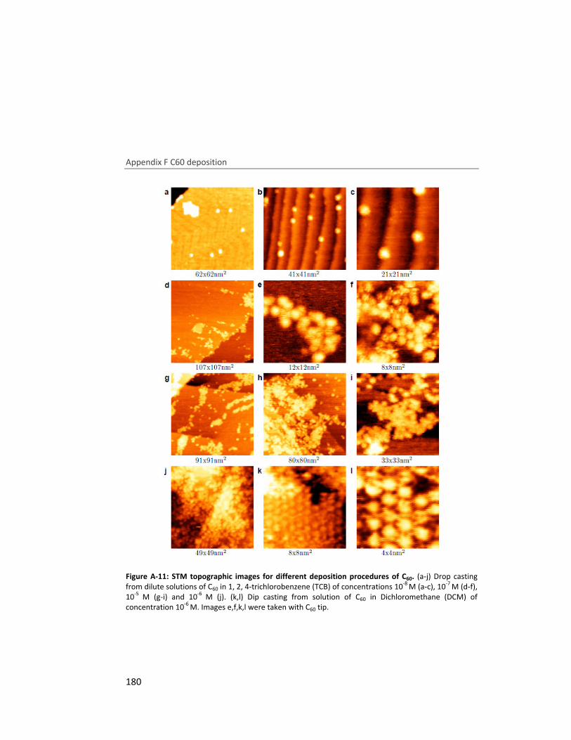
Appendix F C60 deposition
180
Figure A-11: STM topographic images for different deposition procedures of C60. (a-j) Drop casting from dilute solutions of C60 in 1, 2, 4-trichlorobenzene (TCB) of concentrations 10-8 M (a-c), 10-7 M (d-f), 10-5 M (g-i) and 10-6 M (j). (k,l) Dip casting from solution of C60 in Dichloromethane (DCM) of concentration 10-6 M. Images e,f,k,l were taken with C60 tip.
Appendix F C60 deposition
181
References
[Červenka2010] Červenka, J. and C. F. J. Flipse (2010). "Fullerene monolayer formation by spray coating." Nanotechnology 21(6): 065302.
[Gardener2009] Gardener, J. A., G. A. D. Briggs and M. R. Castell (2009). "Scanning tunneling microscopy studies of C_{60} monolayers on Au(111)." Physical Review B 80(23): 235434.
[Guo2004] Guo, S., D. P. Fogarty, P. M. Nagel and S. A. Kandel (2004). "Thermal Diffusion of C60 Molecules and Clusters on Au(111)." The Journal of Physical Chemistry B 108(37): 14074-14081.
[Joachim1995] Joachim, C., J. K. Gimzewski, R. R. Schlittler and C. Chavy (1995). "Electronic Transparence of a Single C_{60} Molecule." Physical Review Letters 74(11): 2102-2105.
[Schull2009] Schull, G., T. Frederiksen, M. Brandbyge and R. Berndt (2009). "Passing Current through Touching Molecules." Physical Review Letters 103(20): 206803.
Appendix G
182
Appendix G
In the experiments
deposited
concentrations close to
annealed gold (1,1,1) substrate. After waiting a couple of minutes, we blew off the
excess solvent and dried the substrate under a stream of argon gas. Then we let the
sample dry for several hour
different concentrations are shown in
10 -11M (
the step edges. More dense individual molecules mainly on step
the terraces g
concentration around 10
terraces and steps, and some small islands of molecules (
concentrations the number of islands and their
Appendix G Dumbbell molecular wires deposition
Appendix G
experiments
ed the molecules from dilute solutions in 1, 2, 4
concentrations close to
annealed gold (1,1,1) substrate. After waiting a couple of minutes, we blew off the
excess solvent and dried the substrate under a stream of argon gas. Then we let the
sample dry for several hour
different concentrations are shown in
M (Figure A-12e,f,
the step edges. More dense individual molecules mainly on step
the terraces gave concentrations close to 10
concentration around 10
terraces and steps, and some small islands of molecules (
concentrations the number of islands and their
Dumbbell molecular wires deposition
DumbbellAppendix G
wires deposition
with dumbbell molecules
the molecules from dilute solutions in 1, 2, 4
concentrations close to 10-5 - 10-8
annealed gold (1,1,1) substrate. After waiting a couple of minutes, we blew off the
excess solvent and dried the substrate under a stream of argon gas. Then we let the
sample dry for several hours. Examples of topographic images of such samples for
different concentrations are shown in
e,f,k,l) give samples with individual molecules mainly located on
the step edges. More dense individual molecules mainly on step
ve concentrations close to 10
concentration around 10-8 M we get samples of individual molecules spread across
terraces and steps, and some small islands of molecules (
concentrations the number of islands and their
Dumbbell molecular wires deposition
Dumbbell
wires deposition
with dumbbell molecules
the molecules from dilute solutions in 1, 2, 48 M by applying several drops to a freshly flame
annealed gold (1,1,1) substrate. After waiting a couple of minutes, we blew off the
excess solvent and dried the substrate under a stream of argon gas. Then we let the
s. Examples of topographic images of such samples for
different concentrations are shown in Figure A-
samples with individual molecules mainly located on
the step edges. More dense individual molecules mainly on step
ve concentrations close to 10
M we get samples of individual molecules spread across
terraces and steps, and some small islands of molecules (
concentrations the number of islands and their
Dumbbell molecular
wires deposition
with dumbbell molecules we mainly
the molecules from dilute solutions in 1, 2, 4-trichlorobenzene (TCB) of
M by applying several drops to a freshly flame
annealed gold (1,1,1) substrate. After waiting a couple of minutes, we blew off the
excess solvent and dried the substrate under a stream of argon gas. Then we let the
s. Examples of topographic images of such samples for
-12a-k. Concentrations close to 10
samples with individual molecules mainly located on
the step edges. More dense individual molecules mainly on step
ve concentrations close to 10 -9M (Figure A
M we get samples of individual molecules spread across
terraces and steps, and some small islands of molecules (Figure A
concentrations the number of islands and their sizes (Figure A
molecular
wires deposition
used drop casting. We
trichlorobenzene (TCB) of
M by applying several drops to a freshly flame
annealed gold (1,1,1) substrate. After waiting a couple of minutes, we blew off the
excess solvent and dried the substrate under a stream of argon gas. Then we let the
s. Examples of topographic images of such samples for
k. Concentrations close to 10
samples with individual molecules mainly located on
the step edges. More dense individual molecules mainly on step-edges and
Figure A-12j). Increasing the
M we get samples of individual molecules spread across
Figure A-12d,I)
Figure A-12a,b,g,h).
molecular
drop casting. We
trichlorobenzene (TCB) of
M by applying several drops to a freshly flamed
annealed gold (1,1,1) substrate. After waiting a couple of minutes, we blew off the
excess solvent and dried the substrate under a stream of argon gas. Then we let the
s. Examples of topographic images of such samples for
k. Concentrations close to 10-10 -
samples with individual molecules mainly located on
edges and a few on
j). Increasing the
M we get samples of individual molecules spread across
I). For higher
g,h).

Appendix G Dumbbell molecular wires deposition
183
Figure A-12: STM topographic images for dumbbell molecular wires deposited with drop casting. (a-l) Dumbbell-type molecule samples deposited with drop casting from dilute solutions in 1, 2, 4-trichlorobenzene (TCB) of concentrations 10-7 M (a,b,g,h), 10-8 M (c,d,i), 10-9 M (j), 10-10 M (e,f,k) and 10-11 M (l).
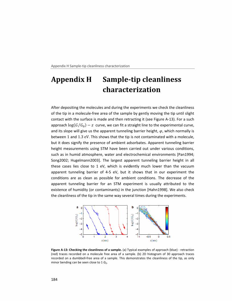
Appendix H
184
Appendix H
After depositing the mo
of the tip in a molecule
contact with the surface is made and then retracting
approach
and its slope will give us the
between
but it does signify the presence of ambient adsorbates.
height measurements using STM have been carried out under various conditions,
such as in humid atmosphere, water and electrochemical environments
Song2002
these cases lies close to 1 eV, which is evidently much lower than the vacuum
apparent tunneling
conditions are as clean as
apparent tunne
existence of humidity (or contaminants) in the junction
the clean
Figure A-13
(red) traces recorded on a molecule free area of a sample. recorded on a dumbbellminor bending can be seen close to 1
Appendix H Sample-tip cleanliness characterization
Appendix H
After depositing the mo
of the tip in a molecule
contact with the surface is made and then retracting
approach log(� � ⁄ )and its slope will give us the
between 1 and 1.3eVt it does signify the presence of ambient adsorbates.
height measurements using STM have been carried out under various conditions,
such as in humid atmosphere, water and electrochemical environments
Song2002; Hugelmann2003
these cases lies close to 1 eV, which is evidently much lower than the vacuum
apparent tunneling barrier of 4
conditions are as clean as
apparent tunneling barrier for an STM experiment is usually attributed to the
existence of humidity (or contaminants) in the junction
he cleanliness of the tip i
13: Checking the cleanliness of a sample.
(red) traces recorded on a molecule free area of a sample. recorded on a dumbbell-free area of a sample. This demonstrates the cleanliness of the tip, as only minor bending can be seen close to 1
tip cleanliness characterization
SampleAppendix H
characterization
After depositing the molecules and during the
of the tip in a molecule-free area of the sample by gently
contact with the surface is made and then retracting) − ¿ curve, we can fit a straight line to the experimental curve,
and its slope will give us the apparent eV. This shows that the tip is not contaminated with a molecule,
t it does signify the presence of ambient adsorbates.
height measurements using STM have been carried out under various conditions,
such as in humid atmosphere, water and electrochemical environments
Hugelmann2003]. The largest
these cases lies close to 1 eV, which is evidently much lower than the vacuum
barrier of 4-
conditions are as clean as possible for ambient conditions
barrier for an STM experiment is usually attributed to the
existence of humidity (or contaminants) in the junction
ness of the tip in the same way several times during the experiments.
Checking the cleanliness of a sample.
(red) traces recorded on a molecule free area of a sample. free area of a sample. This demonstrates the cleanliness of the tip, as only
minor bending can be seen close to 1 G0.
tip cleanliness characterization
Sample-
characterization
and during the experiments we check
free area of the sample by gently
contact with the surface is made and then retracting
curve, we can fit a straight line to the experimental curve,
apparent tunneling barrier height,
. This shows that the tip is not contaminated with a molecule,
t it does signify the presence of ambient adsorbates.
height measurements using STM have been carried out under various conditions,
such as in humid atmosphere, water and electrochemical environments
The largest apparent tunneling
these cases lies close to 1 eV, which is evidently much lower than the vacuum
-5 eV, but it shows that in our experiment the
possible for ambient conditions
barrier for an STM experiment is usually attributed to the
existence of humidity (or contaminants) in the junction
n the same way several times during the experiments.
Checking the cleanliness of a sample. (a) Typical examples of approach (blue)(red) traces recorded on a molecule free area of a sample.
free area of a sample. This demonstrates the cleanliness of the tip, as only
-tip cleanliness
characterization
experiments we check
free area of the sample by gently moving
contact with the surface is made and then retracting it (see
curve, we can fit a straight line to the experimental curve,
tunneling barrier height,
. This shows that the tip is not contaminated with a molecule,
t it does signify the presence of ambient adsorbates. Apparent tunneling b
height measurements using STM have been carried out under various conditions,
such as in humid atmosphere, water and electrochemical environments
apparent tunneling
these cases lies close to 1 eV, which is evidently much lower than the vacuum
5 eV, but it shows that in our experiment the
possible for ambient conditions
barrier for an STM experiment is usually attributed to the
existence of humidity (or contaminants) in the junction [Hahn1998
n the same way several times during the experiments.
Typical examples of approach (blue)(red) traces recorded on a molecule free area of a sample. (b) 2D histogram of 30 approach traces
free area of a sample. This demonstrates the cleanliness of the tip, as only
cleanliness
characterization
experiments we check the
moving the tip until slight
(see Figure A-13)
curve, we can fit a straight line to the experimental curve,
tunneling barrier height, ^, which normally is
. This shows that the tip is not contaminated with a molecule,
Apparent tunneling b
height measurements using STM have been carried out under various conditions,
such as in humid atmosphere, water and electrochemical environments
apparent tunneling barrier height i
these cases lies close to 1 eV, which is evidently much lower than the vacuum
5 eV, but it shows that in our experiment the
possible for ambient conditions. The decrease of the
barrier for an STM experiment is usually attributed to the
Hahn1998]. We also check
n the same way several times during the experiments.
Typical examples of approach (blue)stogram of 30 approach traces
free area of a sample. This demonstrates the cleanliness of the tip, as only
cleanliness
the cleanliness
the tip until slight
). For a such
curve, we can fit a straight line to the experimental curve,
, which normally is
. This shows that the tip is not contaminated with a molecule,
Apparent tunneling barrier
height measurements using STM have been carried out under various conditions,
such as in humid atmosphere, water and electrochemical environments [Pan1994;
barrier height in all
these cases lies close to 1 eV, which is evidently much lower than the vacuum
5 eV, but it shows that in our experiment the
. The decrease of the
barrier for an STM experiment is usually attributed to the
We also check
n the same way several times during the experiments.
Typical examples of approach (blue) - retraction stogram of 30 approach traces
free area of a sample. This demonstrates the cleanliness of the tip, as only
Appendix H Sample-tip cleanliness characterization
185
References
[Hahn1998] Hahn, J. R., Y. A. Hong and H. Kang (1998). "Electron tunneling across an interfacial water layer inside an STM junction: tunneling distance, barrier height and water polarization effect." Applied Physics A 66(1): S467-S472.
[Hugelmann2003] Hugelmann, M. and W. Schindler (2003). "Tunnel barrier height oscillations at the solid/liquid interface." Surface Science 541(1–3): L643-L648.
[Pan1994] Pan, J., T. W. Jing and S. M. Lindsay (1994). "Tunneling Barriers in Electrochemical Scanning Tunneling Microscopy." The Journal of Physical Chemistry 98(16): 4205-4208.
[Song2002] Song, M.-B., J.-M. Jang, S.-E. Bae and C.-W. Lee (2002). "Charge Transfer through Thin Layers of Water Investigated by STM, AFM, and QCM." Langmuir 18(7): 2780-2784.

Appendix I
186
Appendix I
It is well
step-like manner due to atomic rearrangements in the contact
Rubio2001
conductance quantum. A typical conductance histogram for 1,2,3 atom contacts is
dominated by the presence of a peak located very close to
peaks close
are quite sensitive to
breaking speed, environmental conditions,
In our measurements
corresponding to
a result of soft indentations (up to conductance values of
order to check if the shift of the conductance peaks is a result of the small
penetration of the
(~70� � in the
large (Figure A
shorter and they have bigger slopes.
We carried out a statistical a
conductance histogram
curves for the two kinds of indentations
three conductance peaks close to the
(1,2,3 ¡observed for gold atomic contacts, � . In comparison to this histogram the peaks for the soft indentations are slightly
shifted to higher conductance values (see blue histogram
check if this is a rand
made small and large indentations at the same point of contact continuously
Appendix I Conductance of Au atomic contacts
Appendix I
well-known for Au contacts
like manner due to atomic rearrangements in the contact
Rubio2001] with a tendency to exhibit plateaus close to multiples of the
conductance quantum. A typical conductance histogram for 1,2,3 atom contacts is
dominated by the presence of a peak located very close to
peaks close to 2 and
are quite sensitive to
breaking speed, environmental conditions,
In our measurements
corresponding to � are shi
a result of soft indentations (up to conductance values of
order to check if the shift of the conductance peaks is a result of the small
penetration of the tip to the substrate we performed small
) indentations. In
last stages of the breaking of Au wires as a result of soft
Figure A-14b) indentations are shown. The plateaus for soft indentations are
shorter and they have bigger slopes.
We carried out a statistical a
conductance histogram
curves for the two kinds of indentations
three conductance peaks close to the � ). The histogram for the large indentations is the typical histogram
observed for gold atomic contacts,
. In comparison to this histogram the peaks for the soft indentations are slightly
shifted to higher conductance values (see blue histogram
check if this is a random
made small and large indentations at the same point of contact continuously
Conductance of Au atomic contacts
Conductance of Au atomic Appendix I
contacts
Au contacts [
like manner due to atomic rearrangements in the contact
with a tendency to exhibit plateaus close to multiples of the
conductance quantum. A typical conductance histogram for 1,2,3 atom contacts is
dominated by the presence of a peak located very close to
2 and 3 ¡ � ,which are
are quite sensitive to experimental conditions such as temperature, voltage,
breaking speed, environmental conditions,
In our measurements described in chapter
are shifted to slightly higher values.
a result of soft indentations (up to conductance values of
order to check if the shift of the conductance peaks is a result of the small
tip to the substrate we performed small
) indentations. In Figure A
last stages of the breaking of Au wires as a result of soft
indentations are shown. The plateaus for soft indentations are
shorter and they have bigger slopes.
We carried out a statistical analysis out of hundreds of curves and we built the
conductance histogram (Figure A
curves for the two kinds of indentations
three conductance peaks close to the
). The histogram for the large indentations is the typical histogram
observed for gold atomic contacts,
. In comparison to this histogram the peaks for the soft indentations are slightly
shifted to higher conductance values (see blue histogram
om behaviour
made small and large indentations at the same point of contact continuously
Conductance of Au atomic contacts
Conductance of Au atomic
contacts
[Agraït1993],
like manner due to atomic rearrangements in the contact
with a tendency to exhibit plateaus close to multiples of the
conductance quantum. A typical conductance histogram for 1,2,3 atom contacts is
dominated by the presence of a peak located very close to
,which are less pronounced
experimental conditions such as temperature, voltage,
breaking speed, environmental conditions, etc.
described in chapter 6
fted to slightly higher values.
a result of soft indentations (up to conductance values of
order to check if the shift of the conductance peaks is a result of the small
tip to the substrate we performed small
Figure A-14a,b examples of conductance
last stages of the breaking of Au wires as a result of soft
indentations are shown. The plateaus for soft indentations are
shorter and they have bigger slopes.
nalysis out of hundreds of curves and we built the
Figure A-15a) and the 2D
curves for the two kinds of indentations (Figure A
three conductance peaks close to the 1,2,3
). The histogram for the large indentations is the typical histogram
observed for gold atomic contacts, and the peak of one atom cont
. In comparison to this histogram the peaks for the soft indentations are slightly
shifted to higher conductance values (see blue histogram
behaviour in some of the curves or there is a transition
made small and large indentations at the same point of contact continuously
Conductance of Au atomic
contacts
, that the conductanc
like manner due to atomic rearrangements in the contact
with a tendency to exhibit plateaus close to multiples of the
conductance quantum. A typical conductance histogram for 1,2,3 atom contacts is
dominated by the presence of a peak located very close to
less pronounced, although these histo
experimental conditions such as temperature, voltage,
etc. [Yanson1999
(Figure 6-4d) the conductance peaks
fted to slightly higher values. These measurements were
a result of soft indentations (up to conductance values of ~order to check if the shift of the conductance peaks is a result of the small
tip to the substrate we performed small
a,b examples of conductance
last stages of the breaking of Au wires as a result of soft
indentations are shown. The plateaus for soft indentations are
nalysis out of hundreds of curves and we built the
and the 2D- histogram for the breaking
Figure A-15c,d)
multiples of conductance quantum
). The histogram for the large indentations is the typical histogram
the peak of one atom cont
. In comparison to this histogram the peaks for the soft indentations are slightly
shifted to higher conductance values (see blue histogram Figure A
in some of the curves or there is a transition
made small and large indentations at the same point of contact continuously
Conductance of Au atomic
the conductance decreases in a
like manner due to atomic rearrangements in the contact [
with a tendency to exhibit plateaus close to multiples of the
conductance quantum. A typical conductance histogram for 1,2,3 atom contacts is
dominated by the presence of a peak located very close to 1 ¡ � , and by two
lthough these histo
experimental conditions such as temperature, voltage,
Yanson1999].
d) the conductance peaks
These measurements were ~6� ) of the substrate. In
order to check if the shift of the conductance peaks is a result of the small
tip to the substrate we performed small (~6� a,b examples of conductance measurements
last stages of the breaking of Au wires as a result of soft (Figure A
indentations are shown. The plateaus for soft indentations are
nalysis out of hundreds of curves and we built the
histogram for the breaking
c,d). The histogram shows
multiples of conductance quantum
). The histogram for the large indentations is the typical histogram
the peak of one atom contact is located at
. In comparison to this histogram the peaks for the soft indentations are slightly
Figure A-15a). In order to
in some of the curves or there is a transition
made small and large indentations at the same point of contact continuously
Conductance of Au atomic
e decreases in a
[Rubio1996;
with a tendency to exhibit plateaus close to multiples of the
conductance quantum. A typical conductance histogram for 1,2,3 atom contacts is
, and by two
lthough these histograms
experimental conditions such as temperature, voltage,
d) the conductance peaks
These measurements were
of the substrate. In
order to check if the shift of the conductance peaks is a result of the small
) and large
measurements
Figure A-14a) and
indentations are shown. The plateaus for soft indentations are
nalysis out of hundreds of curves and we built the
histogram for the breaking
. The histogram shows
multiples of conductance quantum
). The histogram for the large indentations is the typical histogram
act is located at
. In comparison to this histogram the peaks for the soft indentations are slightly
a). In order to
in some of the curves or there is a transition, we
made small and large indentations at the same point of contact continuously, and
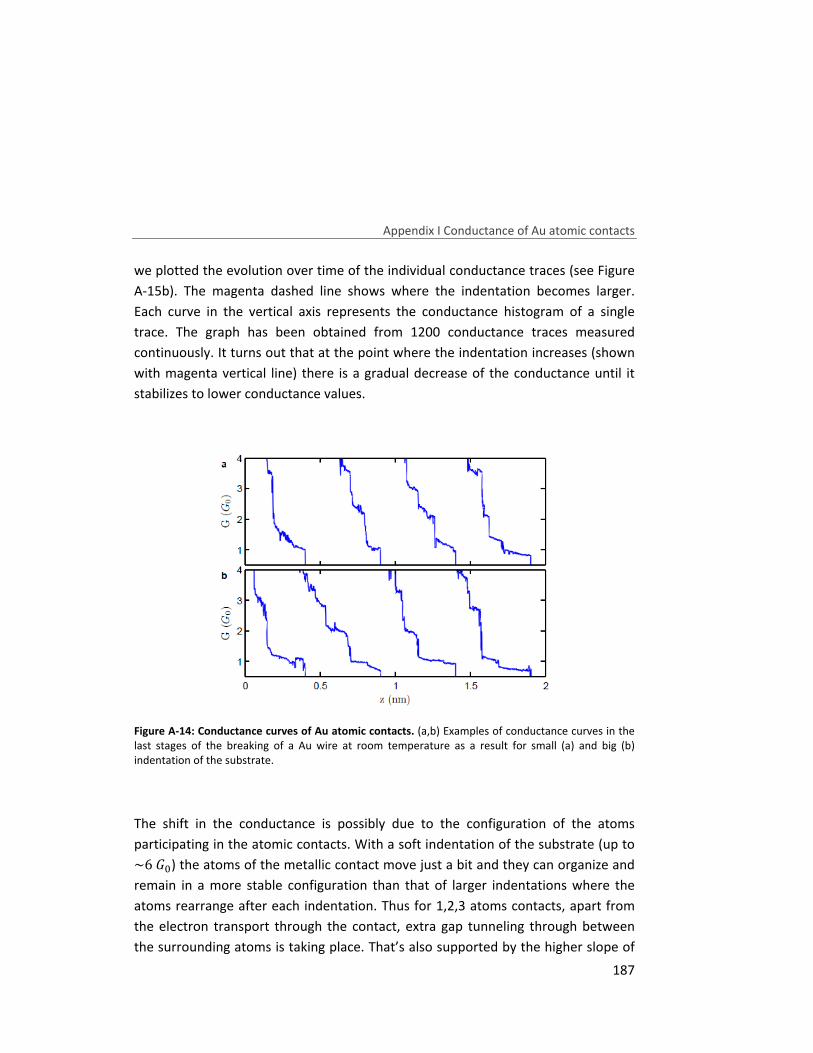
Appendix I Conductance of Au atomic contacts
187
we plotted the evolution over time of the individual conductance traces (see Figure
A-15b). The magenta dashed line shows where the indentation becomes larger.
Each curve in the vertical axis represents the conductance histogram of a single
trace. The graph has been obtained from 1200 conductance traces measured
continuously. It turns out that at the point where the indentation increases (shown
with magenta vertical line) there is a gradual decrease of the conductance until it
stabilizes to lower conductance values.
Figure A-14: Conductance curves of Au atomic contacts. (a,b) Examples of conductance curves in the last stages of the breaking of a Au wire at room temperature as a result for small (a) and big (b) indentation of the substrate.
The shift in the conductance is possibly due to the configuration of the atoms
participating in the atomic contacts. With a soft indentation of the substrate (up to ~6� ) the atoms of the metallic contact move just a bit and they can organize and
remain in a more stable configuration than that of larger indentations where the
atoms rearrange after each indentation. Thus for 1,2,3 atoms contacts, apart from
the electron transport through the contact, extra gap tunneling through between
the surrounding atoms is taking place. That’s also supported by the higher slope of
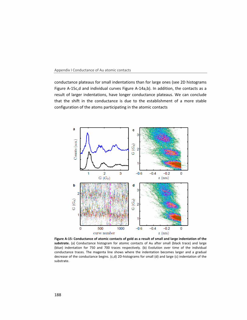
Appendix I Conductance of Au atomic contacts
188
conductance plateaus for small indentations than for large ones (see 2D histograms
Figure A-15c,d and individual curves Figure A-14a,b). In addition, the contacts as a
result of larger indentations, have longer conductance plateaus. We can conclude
that the shift in the conductance is due to the establishment of a more stable
configuration of the atoms participating in the atomic contacts
Figure A-15: Conductance of atomic contacts of gold as a result of small and large indentation of the
substrate. (a) Conductance histogram for atomic contacts of Au after small (black trace) and large (blue) indentation for 750 and 700 traces respectively. (b) Evolution over time of the individual conductance traces. The magenta line shows where the indentation becomes larger and a gradual decrease of the conductance begins. (c,d) 2D-histograms for small (d) and large (c) indentation of the substrate.
Appendix I Conductance of Au atomic contacts
189
References
[Agraït1993] Agraït, N., J. G. Rodrigo and S. Vieira (1993). "Conductance steps and quantization in atomic-size contacts." Physical Review B 47(18): 12345-12348.
[Rubio1996] Rubio, G., N. Agraït and S. Vieira (1996). "Atomic-Sized Metallic Contacts: Mechanical Properties and Electronic Transport." Physical Review Letters 76(13): 2302-2305.
[Rubio2001] Rubio, G., S. R. Bahn, N. Agraït, K. W. Jacobsen and S. Vieira (2001). "Mechanical Properties and Formation Mechanisms of a Wire of Single Gold Atoms." Physical Review Letters 87(2): 026101.
[Yanson1999] Yanson, A. I. (1999). Quantum conductance properties of atomic-size contacts. T. N. Universiteit Leiden.

Appendix J
190
Appendix J
Non equilibrium Green’s function
nanoscale conductors under certain bias
the Hamiltonian of the system contact
corresponding contributions:
where
(ô',�).
Figure A-16
leads.
Green’s function is defined by the following relation:
Appendix J Green’s Functions
Appendix J
Non equilibrium Green’s function
nanoscale conductors under certain bias
the Hamiltonian of the system contact
corresponding contributions:
where t',� describes the interaction between the conductor (
16: Conductor with transmission probability
s function is defined by the following relation:
õ
Green’s Functions
GreenAppendix J
Non equilibrium Green’s function
nanoscale conductors under certain bias
the Hamiltonian of the system contact
corresponding contributions:
describes the interaction between the conductor (
Conductor with transmission probability
s function is defined by the following relation:
õô' t' 0t'H ôÇ t0 t� ô
�+
Green’s Functions
Non equilibrium Green’s function methods are used to calculate the current in
nanoscale conductors under certain bias [Paulsson2002
the Hamiltonian of the system contact-conductor
describes the interaction between the conductor (
Conductor with transmission probability é connected to two large contacts through two
s function is defined by the following relation:
0t�Hô�öõ|Ψ'ø|ΨÇø|Ψ�øö �
� � �+� �
s Functions
methods are used to calculate the current in
Paulsson2002; Ryndyk2009
conductor-contact
describes the interaction between the conductor (
connected to two large contacts through two
s function is defined by the following relation:
øøøö = + õ|Ψ'ø|ΨÇø|Ψ�øö,
� � � .
s Functions
methods are used to calculate the current in
Ryndyk2009]. We divide
contact (see Figure A
describes the interaction between the conductor (ôÇ) and contact
connected to two large contacts through two
øøøö Equation A
Equation A
methods are used to calculate the current in
. We divide
Figure A-16) to the
) and contacts
connected to two large contacts through two
Equation A-12
Equation A-13
Appendix J Green’s Functions
191
Practically, Green’s function will give us the response of a system to a perturbation |ùø in Schrodinger equation |úø = +|úø + |ùø . The response of this perturbation is |úø = −�(+)|ùø. Then, for example, if we want to calculate the wavefunction of
the contact (|Ψ�ø) we can do so if we know the wavefunction of the conductor
(|ΨÇø). From the third row of Equation A-12:
where z� = + − ô�.
Calculating Green’s Function is much easier than solving the Shrodinger equation.
Also, for the case of the conductor, we can just calculate Green’s function of it (�Ç),
without calculating it for the whole system:
By selecting the three equations in the second column of the Green’s functions
matrix, and solving the system we find the Green’s function of the conductor:
where Σ' = t'Hz't' and Σ� = t�Hz�t� are the self-energies (lowercasez is used for
the Green’s functions of the isolated subsystems).
In the case where a bias 7' − 7� is applied in the contact-conductor-contact
system, electrons will be injected and occupy the states corresponding to incoming
waves in contacts. Then we can calculate the wavefunction on the whole system
caused by the incoming wave in contact 1. The wavefunction now is changing to üΨ',Aý + |Ψhøü (|Ψ',Aý is the totally reflected wave and |Ψhø is the retarded
response of the whole system. Using this wavefunction in the Shrodinger equation
we find the device wavefunction and the wavefunction in contact 1:
ô�|Ψ�ø + t�|ΨÇø = +|Ψ�ø ⇒ |Ψ�ø = z�(+)t�|ΨÇø, Equation A-14
õ+ − ô' t' 0t'H + − ôÇ t�H0 t� + − ô�öþ�' �'Ç �'��Ç' �Ç �Ç���' ��Ç �� �
= þ 0 00 00 0 �. Equation A-15
�a = (+ − �a − Σ' − Σ�)�', Equation A-16
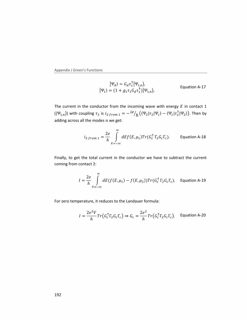
Appendix J Green’s Functions
192
The current in the conductor from the incoming wave with energy + in contact 1
(|Ψ',Aý) with coupling t� is -�wxÉP' = − - ℏ� ��Ψ�|t�|ΨÇø − �ΨÇ|t�H|Ψ�ø�. Then by
adding across all the modes ? we get:
Finally, to get the total current in the conductor we have to subtract the current
coming from contact 2:
For zero temperature, it reduces to the Landauer formula:
üΨaø = �at'HüΨ',Aý, üΨ'ø = (1 + z't'�at'H)üΨ',Aý, Equation A-17
-�wxÉP' = 2ℎ 6 �+&(+, 7')��(�ÇHMQ�M
Γ��ÇΓÇ). Equation A-18
= 2ℎ 6 �+(&(+, 7') − &(+, 7�))��(�ÇHMQ�M
Γ��ÇΓÇ). Equation A-19
= 2��ℎ ����ÇHΓ��ÇΓÇ� ⇒ �Ç = 2�ℎ ����ÇHΓ��ÇΓÇ�. Equation A-20
Appendix J Green’s Functions
193
References
[Paulsson2002] Paulsson, M. (2002). "Non Equilibrium Green's Functions for Dummies: Introduction to the One Particle NEGF equations." arXiv:cond-mat/0210519.
[Ryndyk2009] Ryndyk, D. A., R. Gutiérrez, B. Song and G. Cuniberti (2009). Green Function Techniques in the Treatment of Quantum Transport at the Molecular Scale. Energy Transfer Dynamics in Biomaterial Systems. I. Burghardt, V. May, D. A. Micha and E. R. Bittner, Springer Berlin Heidelberg. 93: 213-335.
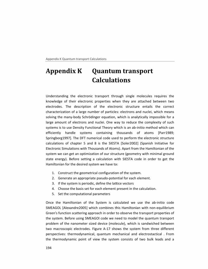
Appendix K
194
Appendix K
Understanding the electronic transport through single molecule
knowledge of their electronic properties when they are attached between two
electrodes. The description of the electronic structure entails the correct
characterization of a large number of particles: electrons and
solving the many
large amount of electrons and nucle
systems is to use Density Functional Theory which is an ab
efficiently handl
Springborg1997
calculations
Electronic Simulations with Thousands of Atoms). Apart from the Hamiltoni
system we can get an optimization of our structure (geometry with minimal ground
state energy). Before setting a calculation with SIESTA code in order to get the
Hamiltonian for the desired system we have to
1. Construct the geometrical configurati
2. Generate an appropriate pseudo
3. If the system is periodic, define the lattice vectors
4. Choose the basis set for each element present in the calculation.
5. Set the computational parameters
Once the Hamiltonian of t
SMEAGOL
Green's function scattering approach in order to observe the transport properties of
the system. Before
problem of the nanometer sized device (molecule), which is sandwiched between
two macroscopic e
perspectives
the thermodynamic point of view the system consists of two bulk leads and a
Appendix K Quantum transport Calculations
Appendix K
Understanding the electronic transport through single molecule
knowledge of their electronic properties when they are attached between two
electrodes. The description of the electronic structure entails the correct
characterization of a large number of particles: electrons and
g the many-body Schrödinger equation, which is
large amount of electrons and nucle
systems is to use Density Functional Theory which is an ab
efficiently handle systems containing thousands of atoms
Springborg1997]. The DFT numerical code used
calculations of chapter
Electronic Simulations with Thousands of Atoms). Apart from the Hamiltoni
system we can get an optimization of our structure (geometry with minimal ground
state energy). Before setting a calculation with SIESTA code in order to get the
Hamiltonian for the desired system we have to
Construct the geometrical configurati
Generate an appropriate pseudo
If the system is periodic, define the lattice vectors
Choose the basis set for each element present in the calculation.
Set the computational parameters
Once the Hamiltonian of t
SMEAGOL [Alexandre2005
reen's function scattering approach in order to observe the transport properties of
system. Before using SMEAGOl code we need to model the quantum transport
problem of the nanometer sized device (molecule), which is sandwiched between
two macroscopic electrodes.
perspectives: thermodynamical,
the thermodynamic point of view the system consists of two bulk leads and a
Quantum transport Calculations
Quantum Appendix K
Calculations
Understanding the electronic transport through single molecule
knowledge of their electronic properties when they are attached between two
electrodes. The description of the electronic structure entails the correct
characterization of a large number of particles: electrons and
body Schrödinger equation, which is
large amount of electrons and nucle
systems is to use Density Functional Theory which is an ab
e systems containing thousands of atoms
The DFT numerical code used
of chapter 5 and 8
Electronic Simulations with Thousands of Atoms). Apart from the Hamiltoni
system we can get an optimization of our structure (geometry with minimal ground
state energy). Before setting a calculation with SIESTA code in order to get the
Hamiltonian for the desired system we have to
Construct the geometrical configurati
Generate an appropriate pseudo
If the system is periodic, define the lattice vectors
Choose the basis set for each element present in the calculation.
Set the computational parameters
Once the Hamiltonian of the System is calculated we use the ab
Alexandre2005] which combines this Hamiltonian with non
reen's function scattering approach in order to observe the transport properties of
using SMEAGOl code we need to model the quantum transport
problem of the nanometer sized device (molecule), which is sandwiched between
lectrodes. Figure A
: thermodynamical, quantum mechanical and
the thermodynamic point of view the system consists of two bulk leads and a
Quantum transport Calculations
Quantum
Calculations
Understanding the electronic transport through single molecule
knowledge of their electronic properties when they are attached between two
electrodes. The description of the electronic structure entails the correct
characterization of a large number of particles: electrons and
body Schrödinger equation, which is
large amount of electrons and nuclei. One way to reduce the complexity of such
systems is to use Density Functional Theory which is an ab
e systems containing thousands of atoms
The DFT numerical code used
is the SIESTA
Electronic Simulations with Thousands of Atoms). Apart from the Hamiltoni
system we can get an optimization of our structure (geometry with minimal ground
state energy). Before setting a calculation with SIESTA code in order to get the
Hamiltonian for the desired system we have to
Construct the geometrical configuration of the system.
Generate an appropriate pseudo-potential for each element.
If the system is periodic, define the lattice vectors
Choose the basis set for each element present in the calculation.
Set the computational parameters
he System is calculated we use the ab
which combines this Hamiltonian with non
reen's function scattering approach in order to observe the transport properties of
using SMEAGOl code we need to model the quantum transport
problem of the nanometer sized device (molecule), which is sandwiched between
Figure A-17 show
quantum mechanical and
the thermodynamic point of view the system consists of two bulk leads and a
Quantum transport
Calculations
Understanding the electronic transport through single molecule
knowledge of their electronic properties when they are attached between two
electrodes. The description of the electronic structure entails the correct
characterization of a large number of particles: electrons and
body Schrödinger equation, which is analytically
. One way to reduce the complexity of such
systems is to use Density Functional Theory which is an ab-
e systems containing thousands of atoms
The DFT numerical code used to perform the electronic structure
is the SIESTA [Soler2002
Electronic Simulations with Thousands of Atoms). Apart from the Hamiltoni
system we can get an optimization of our structure (geometry with minimal ground
state energy). Before setting a calculation with SIESTA code in order to get the
Hamiltonian for the desired system we have to:
on of the system.
potential for each element.
If the system is periodic, define the lattice vectors
Choose the basis set for each element present in the calculation.
he System is calculated we use the ab
which combines this Hamiltonian with non
reen's function scattering approach in order to observe the transport properties of
using SMEAGOl code we need to model the quantum transport
problem of the nanometer sized device (molecule), which is sandwiched between
shows the system
quantum mechanical and
the thermodynamic point of view the system consists of two bulk leads and a
ransport
Understanding the electronic transport through single molecules requires the
knowledge of their electronic properties when they are attached between two
electrodes. The description of the electronic structure entails the correct
characterization of a large number of particles: electrons and nuclei, which
analytically impossible for a
. One way to reduce the complexity of such
-initio method which can
e systems containing thousands of atoms
to perform the electronic structure
Soler2002] (Spanish Initiative for
Electronic Simulations with Thousands of Atoms). Apart from the Hamiltoni
system we can get an optimization of our structure (geometry with minimal ground
state energy). Before setting a calculation with SIESTA code in order to get the
on of the system.
potential for each element.
Choose the basis set for each element present in the calculation.
he System is calculated we use the ab
which combines this Hamiltonian with non-
reen's function scattering approach in order to observe the transport properties of
using SMEAGOl code we need to model the quantum transport
problem of the nanometer sized device (molecule), which is sandwiched between
s the system from three different
quantum mechanical and electrostactical
the thermodynamic point of view the system consists of two bulk leads and a
s requires the
knowledge of their electronic properties when they are attached between two
electrodes. The description of the electronic structure entails the correct
which means
impossible for a
. One way to reduce the complexity of such
initio method which can
[Parr1989;
to perform the electronic structure
(Spanish Initiative for
Electronic Simulations with Thousands of Atoms). Apart from the Hamiltonian of the
system we can get an optimization of our structure (geometry with minimal ground
state energy). Before setting a calculation with SIESTA code in order to get the
Choose the basis set for each element present in the calculation.
he System is calculated we use the ab-initio code
-equilibrium
reen's function scattering approach in order to observe the transport properties of
using SMEAGOl code we need to model the quantum transport
problem of the nanometer sized device (molecule), which is sandwiched between
from three different
lectrostactical . From
the thermodynamic point of view the system consists of two bulk leads and a

Appendix K Quantum transport Calculations
195
central region which includes the molecule and a part of the leads. The two leads
are in different chemical potentials (7g , 7h) which, if they are equal, the system is in
thermodynamic equilibrium and if they are different (bias voltage applied) current
will flow.
Figure A-17: Schematic representation of the transport problem from three different perspectives.
(a) Thermodynamical. (b) Quantum mechanical. (c) Electrostactical.[Rocha2007]
In the Quantum mechanical point of view (Figure A-17b), modeling of the
macroscopic electrodes as infinitely long leads with infinite cross-sections with the
finite scattering region in the middle EM (Extended Molecule) will result in the
Hamiltonian of the system being an infinite Hermitian matrix (ℋ). In order to avoid
that, we make two assumptions:
1. Leads are semi-infinite defect-free crystalline metals, and the Hamiltonian
will have a regular periodic structure and a unit cell along which the
direction of the transport can be calculated.
2. Periodic boundary conditions are used in order to avoid the infinite cross-
section. The system is repeated periodically in the transverse direction.
Then in order to further simplify the problem we introduce the concept of a
principal layer (PL), which is the smallest cell that repeats periodically in the

Appendix K Quantum transport Calculations
196
direction of transport, and is constructed in a way that it interacts only with the
next neighbored principal layer. We define ô (the ° × °matrix describing all
interactions in a PL), ô' (the � ×� matrix describing the interactions between the
PLs), ôg» and ôh» (the matrix describing the interaction between the last PLs and
the extended molecule at the left hand side and right hand side respectively).
Finally, ℋtakes the following form:
ℋ now has the same structure as the Hamiltonian of one-dimensional chain but
with block elements instead of chains. In the electrostatic point of view (Figure A-
17c) an external bias voltage applied on the leads will produce a rigid shift of the
whole spectrum which will lead to a non-trivial potential profile over the EM which
will need to be calculated self-consistently. The resulting potential must match one
of the leads at the boundaries of the EM, in order not to develop a discontinuity
with the generation of spurious scattering. Therefore, in order to achieve a good
match of the electrostatic potential, several layers of the leads are usually included
in the extended molecule.
Then, by assuming that states deep inside the electrodes are scattered by the
potential created by the central EM, Green’s Functions techniques [Datta1997] are
used to calculate the ground state electronic properties of the system. Finally, at
the zero-bias limit using the Landauer-Buttiker formalism [Büttiker1985], the
conductance of the scatterer is calculated.[Rocha2007]
ℋ =�������⋱ ô' 0 . . . .ô'H ô ô' 0 . . .0 ô'H ô ôg» 0 . .. 0 ô»g ô» ô»h 0 .. . 0 ôh» ô ô' 0. . . 0 ô'H ô ô'. . . . 0 ô'H ⋱
������. Equation A-21

Appendix K Quantum transport Calculations
197
References
[Alexandre2005] Alexandre, R. R., M. G.-s. Víctor, W. B. Steve, J. L. Colin, F. Jaime, et al. (2005). "Towards molecular spintronics." Nature Materials 4(4): 335-339.
[Büttiker1985] Büttiker, M., Y. Imry, R. Landauer and S. Pinhas (1985). "Generalized many-channel conductance formula with application to small rings." Physical Review B 31(10): 6207-6215.
[Datta1997] Datta, S. (1997). Electronic Transport in Mesoscopic Systems, Cambridge University Press.
[Parr1989] Parr, R. G. and W. Yang (1989). Density-Functional Theory of Atoms and Molecules, Oxford University Press, USA.
[Rocha2007] Rocha, A. R. (2007). Theoretical and Computational Aspects of electronic transport at the Nanoscale. PhD, University of Dublin.
[Soler2002] Soler, J. M., E. Artacho, J. D. Gale, A. García, J. Junquera, et al. (2002). "The SIESTA method for ab initio order-N materials simulation." J. Phys.: Condens. Matter 14(2745).
[Springborg1997] Springborg, M. (1997). Density-functional methods in chemistry and materials science, Wiley.

[1]
C. Evangeli
Agraït
[2]
Dumbbell Junctions
K. Gi
G. Rubio
3822 (2013)
[3]
Dumbbell
A. La Rosa, K. Gillemot, E. Leary,
Lambert, N
J. Org. Chem. 79, 4871
[4]
C. Evangeli
Cuevas, and N
submitted to Nano Letters (october 2014)
[5]
E. Leary,
[1] Engineering the Thermopower of C
C. Evangeli, K. Gillemot, E., M. T. González, G. Rubio
Agraït. Nano Letters
[2] A Detailed Experimental and Theoretical Study into the Properties of C
Dumbbell Junctions
K. Gillemot, C. Evangeli
G. Rubio-Bollinger, J. Ferrer, N. Martín , C. J. Lambert, N. Agraït
3822 (2013).
[3] Does the Cyclopropane Ring Enhance the Electronic Communication in
Dumbbell-type C
A. La Rosa, K. Gillemot, E. Leary,
Lambert, N. Martín
J. Org. Chem. 79, 4871
[4] Quantum thermopower of metallic atomic
Evangeli, M. Matt, L
Cuevas, and N. Agraït
submitted to Nano Letters (october 2014)
[5] Locating the levels in dithiafulvalene functionalized molecular wires
Leary, C. Evangeli
Engineering the Thermopower of C
, K. Gillemot, E., M. T. González, G. Rubio
Nano Letters 13, 2141
A Detailed Experimental and Theoretical Study into the Properties of C
Dumbbell Junctions
C. Evangeli, E. Leary, A. La Rosa, M. T. González, S. Filippone, I. Grace ,
Bollinger, J. Ferrer, N. Martín , C. J. Lambert, N. Agraït
Does the Cyclopropane Ring Enhance the Electronic Communication in
type C60 dimers?
A. La Rosa, K. Gillemot, E. Leary,
Martín
J. Org. Chem. 79, 4871-4877 (2014)
Quantum thermopower of metallic atomic
Matt, L. Rincón
Agraït
submitted to Nano Letters (october 2014)
Locating the levels in dithiafulvalene functionalized molecular wires
Evangeli, M. T. González, G
Engineering the Thermopower of C60 M
, K. Gillemot, E., M. T. González, G. Rubio
, 2141-5 (2013).
A Detailed Experimental and Theoretical Study into the Properties of C
, E. Leary, A. La Rosa, M. T. González, S. Filippone, I. Grace ,
Bollinger, J. Ferrer, N. Martín , C. J. Lambert, N. Agraït
Does the Cyclopropane Ring Enhance the Electronic Communication in
A. La Rosa, K. Gillemot, E. Leary, C. Evangeli
4877 (2014).
Quantum thermopower of metallic atomic
Rincón-García, F. Pauly, P
submitted to Nano Letters (october 2014)
Locating the levels in dithiafulvalene functionalized molecular wires
González, G. Rubio
Molecular Junctions.
, K. Gillemot, E., M. T. González, G. Rubio-Bollinger, C. J. Lambert, and N.
A Detailed Experimental and Theoretical Study into the Properties of C
, E. Leary, A. La Rosa, M. T. González, S. Filippone, I. Grace ,
Bollinger, J. Ferrer, N. Martín , C. J. Lambert, N. Agraït
Does the Cyclopropane Ring Enhance the Electronic Communication in
C. Evangeli, T. Gonzalez, S
Quantum thermopower of metallic atomic-size contacts at room temperature
Pauly, P.r Nielaba,
submitted to Nano Letters (october 2014)
Locating the levels in dithiafulvalene functionalized molecular wires
Rubio-Bollinger, N
olecular Junctions.
Bollinger, C. J. Lambert, and N.
A Detailed Experimental and Theoretical Study into the Properties of C
, E. Leary, A. La Rosa, M. T. González, S. Filippone, I. Grace ,
Bollinger, J. Ferrer, N. Martín , C. J. Lambert, N. Agraït. Small
Does the Cyclopropane Ring Enhance the Electronic Communication in
Gonzalez, S. Filippone, N
size contacts at room temperature
r Nielaba, G. Rubio
Locating the levels in dithiafulvalene functionalized molecular wires
Bollinger, N. Agraït, in
Publication List
Bollinger, C. J. Lambert, and N.
A Detailed Experimental and Theoretical Study into the Properties of C60
, E. Leary, A. La Rosa, M. T. González, S. Filippone, I. Grace ,
Small 9, 3812–
Does the Cyclopropane Ring Enhance the Electronic Communication in
Filippone, N. Agraït, C
size contacts at room temperature
Rubio-Bollinger, J
Locating the levels in dithiafulvalene functionalized molecular wires
Agraït, in preparation
Publication List
199
Bollinger, C. J. Lambert, and N.
, E. Leary, A. La Rosa, M. T. González, S. Filippone, I. Grace ,
Agraït, C. J.
size contacts at room temperature
Bollinger, J. C.
preparation.


![[PPT]Hubungan antar sel (Pertautan Antar Sel)= Cell junctions · Web viewHubungan antar sel (Pertautan Antar Sel)= Cell junctions Cell junctions merupakan situs hubungan yang menghubungkan](https://img.pdfslide.tips/doc/110x75/5ad8f86f7f8b9af9068e3250/ppthubungan-antar-sel-pertautan-antar-sel-cell-junctions-viewhubungan-antar.jpg)