Embed Size (px)
Citation preview

Ti T i k d TTips, Tricks, and Traps of High Power Semiconductor Device Testing
张卫华
KEITHLEY INSTRUMENTS
1 8/20/2012 © 2012 Keithley Instruments, Inc.© 2012 Keithley Instruments, Inc.
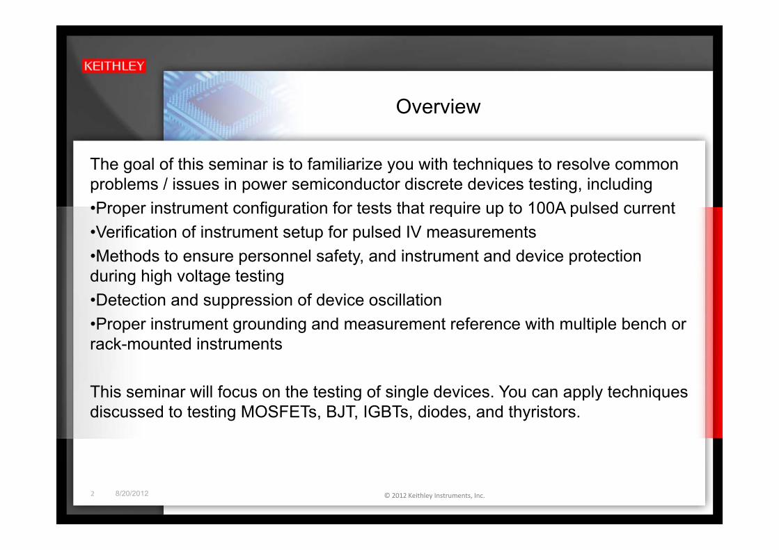
Overview
The goal of this seminar is to familiarize you with techniques to resolve common problems / issues in power semiconductor discrete devices testing, including•Proper instrument configuration for tests that require up to 100A pulsed currentProper instrument configuration for tests that require up to 100A pulsed current•Verification of instrument setup for pulsed IV measurements•Methods to ensure personnel safety, and instrument and device protection during high voltage testingduring high voltage testing•Detection and suppression of device oscillation•Proper instrument grounding and measurement reference with multiple bench or rack-mounted instruments
This seminar will focus on the testing of single devices. You can apply techniques g g pp y qdiscussed to testing MOSFETs, BJT, IGBTs, diodes, and thyristors.
2 8/20/2012 © 2012 Keithley Instruments, Inc.
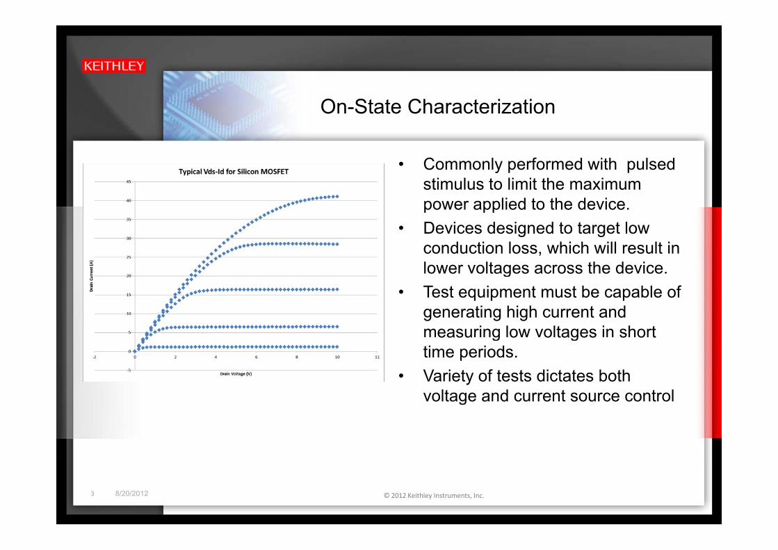
On-State Characterization
• Commonly performed with pulsed stimulus to limit the maximum power applied to the device. p pp
• Devices designed to target low conduction loss, which will result in lower voltages across the device. g
• Test equipment must be capable of generating high current and measuring low voltages in short easu g o o tages s o ttime periods.
• Variety of tests dictates both voltage and current source controlvoltage and current source control
3 8/20/2012 © 2012 Keithley Instruments, Inc.

Keithley solutions for on-state characterization
K ithl S i 2600AKeithley Series 2600A System SourceMeter Instrument
Keithley Model 2651A High Power System S M t I t tSourceMeter Instrument
4 8/20/2012 © 2012 Keithley Instruments, Inc.
Another solution for the lower voltage control is Keithley’s Model 4200 Semiconductor Characterization System
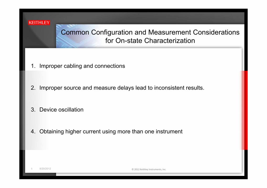
C C fi ti d M t C id tiCommon Configuration and Measurement Considerations for On-state Characterization
1. Improper cabling and connections
2. Improper source and measure delays lead to inconsistent results.
3. Device oscillation
4. Obtaining higher current using more than one instrument
5 8/20/2012 © 2012 Keithley Instruments, Inc.

Why Cabling Matters for High Current Testing
• Devices that can carry a lot of current are typically low resistance in order to minimize conduction loss
– Will require sensitive voltage measurement. q g• Must consider impact of cabling and connections
– Cable must be rated for the test current in order to avoid fire hazard– Resistance of test leads / traces may be large relative to DUT resistanceResistance of test leads / traces may be large relative to DUT resistance– Large currents are more sensitive to test system inductance
6 8/20/2012 © 2012 Keithley Instruments, Inc.
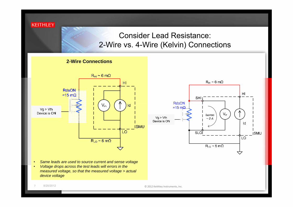
C id L d R i tConsider Lead Resistance: 2-Wire vs. 4-Wire (Kelvin) Connections
2-Wire Connections
• Same leads are used to source current and sense voltage• Voltage drops across the test leads will errors in the
measured voltage, so that the measured voltage > actual
7 8/20/2012 © 2012 Keithley Instruments, Inc.
device voltage
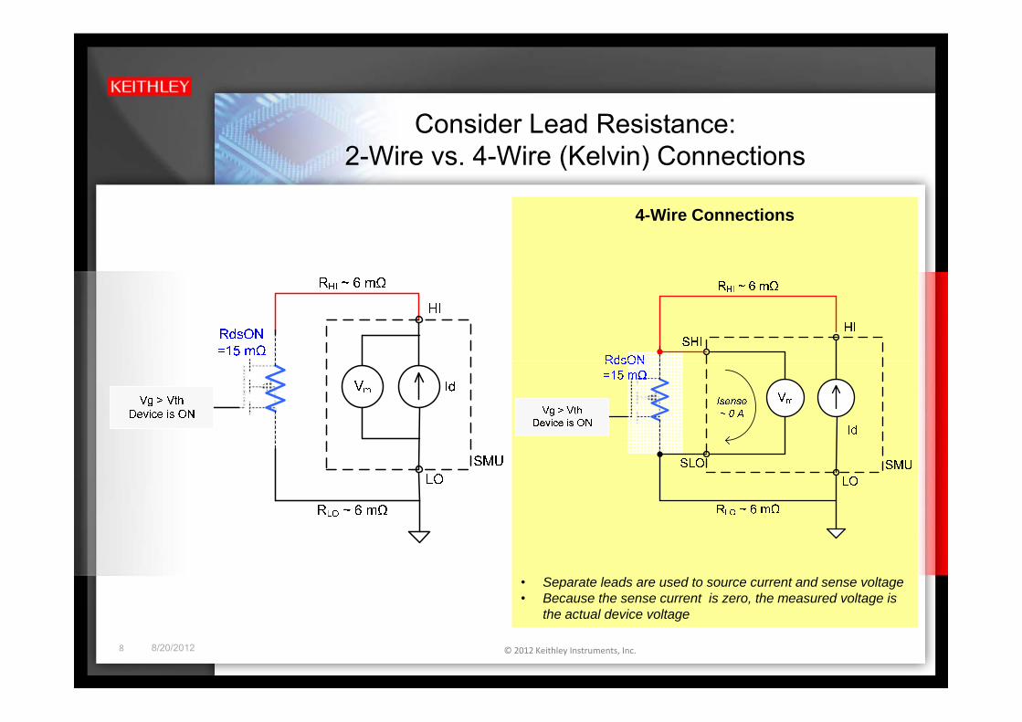
C id L d R i tConsider Lead Resistance: 2-Wire vs. 4-Wire (Kelvin) Connections
4-Wire Connections
• Separate leads are used to source current and sense voltage• Because the sense current is zero, the measured voltage is
8 8/20/2012 © 2012 Keithley Instruments, Inc.
the actual device voltage
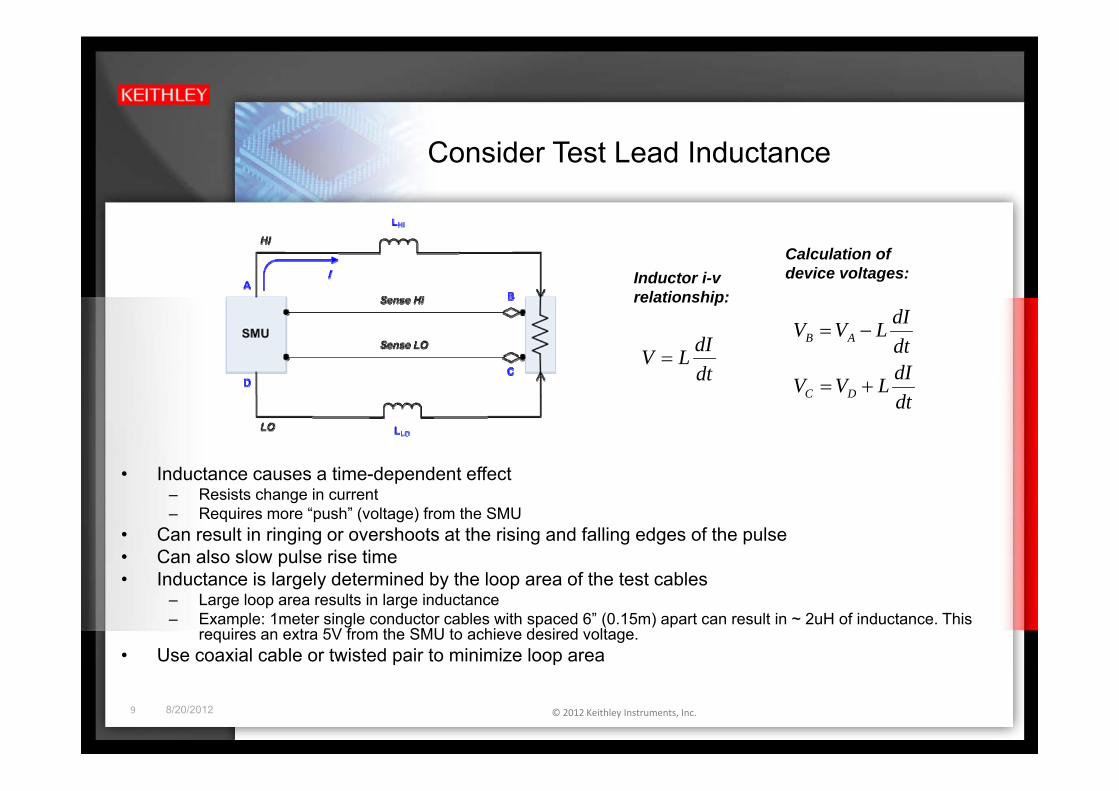
Consider Test Lead Inductance
Inductor i-v relationship:
Calculation of device voltages:
dtdILV =
ddILVV
dtdILVV
DC
AB
+=
−=
• Inductance causes a time-dependent effect
dtDC
– Resists change in current– Requires more “push” (voltage) from the SMU
• Can result in ringing or overshoots at the rising and falling edges of the pulse• Can also slow pulse rise time
I d t i l l d t i d b th l f th t t bl• Inductance is largely determined by the loop area of the test cables– Large loop area results in large inductance – Example: 1meter single conductor cables with spaced 6” (0.15m) apart can result in ~ 2uH of inductance. This
requires an extra 5V from the SMU to achieve desired voltage.• Use coaxial cable or twisted pair to minimize loop area
9 8/20/2012 © 2012 Keithley Instruments, Inc.
p p

Tips for Optimal Cabling
• Minimizing effects of lead resistance– Always use wire of the appropriate gauge for required level of current
• Example: 20A DC requires 12 AWG or lowerp q
– Minimize contact resistance• Ensure contacts are clean• Ensure connections are secure• Ensure good solder joints• Ensure good solder joints
– Use 4-wire (Kelvin) connections
Minimizing Inductance• Minimizing Inductance– Minimize loop area by twisting test leads together to form a twisted pair– Use coaxial cable
• The Keithley Model 2651A High Power SourceMeter instrument includes a low resistance, low inductance coaxial cable
10 8/20/2012 © 2012 Keithley Instruments, Inc.
– Cable is rated 3mΩ and 85nH per meter
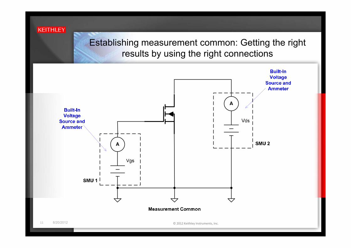
E t bli hi t G tti th i htEstablishing measurement common: Getting the right results by using the right connections
11 8/20/2012 © 2012 Keithley Instruments, Inc.
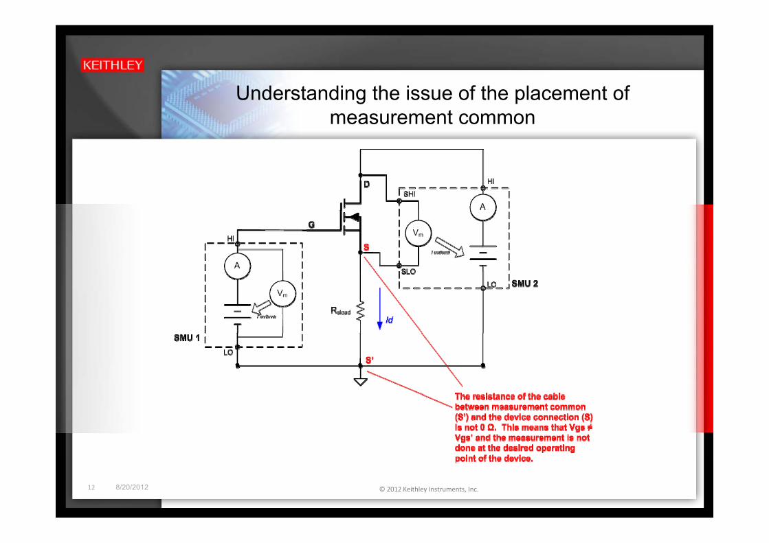
U d t di th i f th l t fUnderstanding the issue of the placement of measurement common
12 8/20/2012 © 2012 Keithley Instruments, Inc.
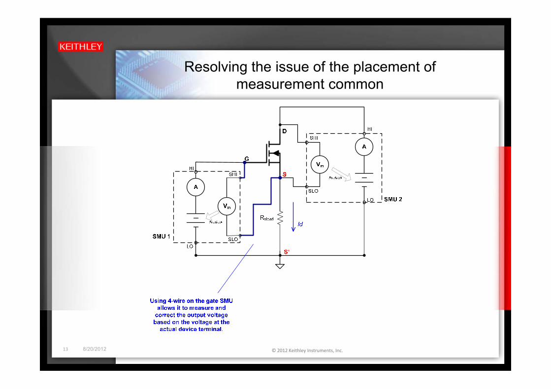
R l i th i f th l t fResolving the issue of the placement of measurement common
13 8/20/2012 © 2012 Keithley Instruments, Inc.
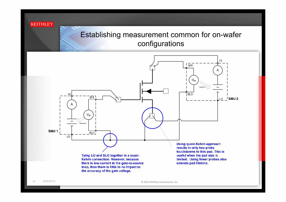
E t bli hi t f fEstablishing measurement common for on-wafer configurations
14 8/20/2012 © 2012 Keithley Instruments, Inc.
S G tti th i ht lt b i th i htSummary: Getting the right results by using the right connections
• Use 4-Wire for connecting to the gate SMU to ensure that source lead resistance doesn’t impact accuracy of Vgs
• Route the LO terminal of the high current SMU separately from the common terminal of the rest of the SMUs. Ensures that high current doesn’t cause voltage errorsvoltage errors.
• For on-wafer testing: If pad space is limited or pad lifetime is a concern, consider using quasi Kelvin approach where you tie Force and Senseconsider using quasi-Kelvin approach where you tie Force and Sense terminals together as close as possible to the DUT
15 8/20/2012 © 2012 Keithley Instruments, Inc.
System Validation
• Validate your system to ensure that the system is properly configured and to have confidence that you’re getting correct measurements.
• ConsiderConsider– Connections– Pulse Fidelity
16 8/20/2012 © 2012 Keithley Instruments, Inc.
System Validation: Getting the desired results
• Make sure that all of the instrument terminals are connected to the device terminals
– The Model 2651A has contact check feature that enables user to verify that the yboth force and sense terminals are connected prior to a test
• Output a single pulse and measure the response at the DUT to configure appropriate source and measure delayspp p y
– High speed digitizers are useful for measuring the pulse response– In addition to two high resolution integrating ADCs, the Model 2651A has two 1MHz
18-bit digitizers (fast ADC) for measuring voltage and current simultaneously
17 8/20/2012 © 2012 Keithley Instruments, Inc.
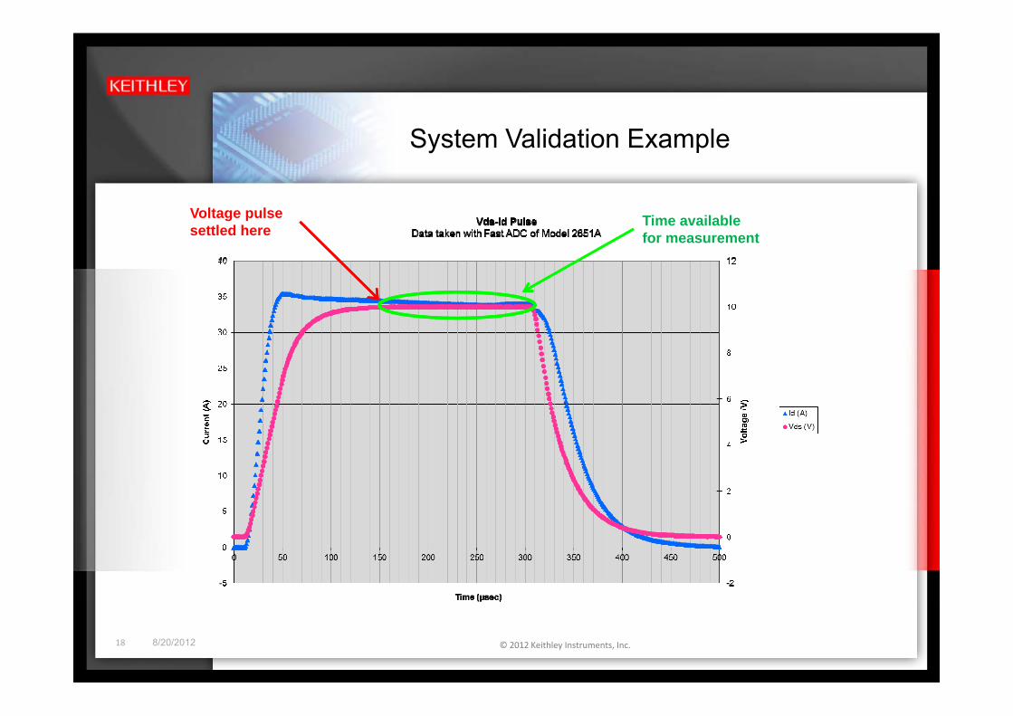
System Validation Example
Voltage pulse settled here Time available
for measurement
18 8/20/2012 © 2012 Keithley Instruments, Inc.

Oscillation in High Power Semi Devices
• Commonly present in high gain and high switching speed transistors.• Can destroy the device.• Results in inconsistent and erroneous measurements
Reasons for oscillation:• Feedback-type oscillation when variation in device output voltage coupled toFeedback type oscillation when variation in device output voltage coupled to
device input – Large changes in impedance as device is switched from off-state to on-state result
in variations in the output voltage – Because the gate is coupled to output by the reverse transfer capacitance, the
output voltage variations inject energy into gate terminal. This is fed back to output and results in oscillation.
• Resonant tank circuit created by parasitic inductances and capacitances of• Resonant tank circuit created by parasitic inductances and capacitances of device, driver circuit, and connections to the device input terminal.
• Interactions between multiple instruments connected to different device terminals.
19 8/20/2012 © 2012 Keithley Instruments, Inc.
terminals.
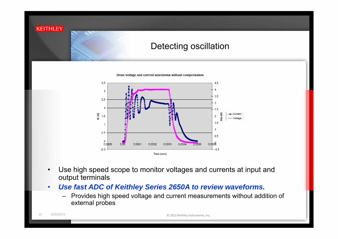
Detecting oscillation
• Use high speed scope to monitor voltages and currents at input and output terminals
• Use fast ADC of Keithley Series 2650A to review waveforms. – Provides high speed voltage and current measurements without addition of
t l b20 8/20/2012 © 2012 Keithley Instruments, Inc.
external probes
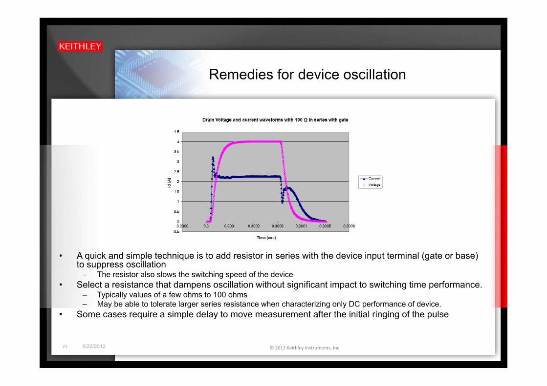
Remedies for device oscillation
• A quick and simple technique is to add resistor in series with the device input terminal (gate or base) to suppress oscillation
– The resistor also slows the switching speed of the device• Select a resistance that dampens oscillation without significant impact to switching time performance.
– Typically values of a few ohms to 100 ohms– May be able to tolerate larger series resistance when characterizing only DC performance of device.
• Some cases require a simple delay to move measurement after the initial ringing of the pulse
21 8/20/2012 © 2012 Keithley Instruments, Inc.

Remedies for device oscillation
• Other techniques include • Establish local ground loop by tying cable shields together as close as possible to
the DUT• Use of ferrite beads around connections to device input terminal • Use RC compensation circuits for parasitic capacitances and inductances at the
device input terminal• Use shunt capacitor across output of device
• Reduce response time of SMU connected to input terminal • On some Keithley SMUs, this is done by enabling High-Capacitance (“Hi-C”) modey , y g g p ( )
22 8/20/2012 © 2012 Keithley Instruments, Inc.

I ti i t i i ith d i i t K ithlInserting resistor in series with device input on Keithley Model 8010 High Power Test Fixture
23 8/20/2012 © 2012 Keithley Instruments, Inc.
T ti ith hi h t b d th bilit fTesting with even higher current, beyond the capability of a single SMU
• SMUs can be used in parallel to achieve higher currents or longer pulse widths or higher duty cycle pulse trains
– May be used for current sourcing or voltage sourcing test configurationsy g g g g• Combining SMUs is an advanced topic. In order to achieve consistent and
accurate results, you must take proper design considerations– See Model 2651A-related apps note on Keithley website (http://www keithley com)See Model 2651A related apps note on Keithley website (http://www.keithley.com)
• Keithley TSPExpress and ACS Basic Edition software packages simplify the SMU configuration and deliver precise measurements when using two SMUs in parallelin parallel
• Let’s see how SMUs can be used in parallel for two common MOSFET tests
24 8/20/2012 © 2012 Keithley Instruments, Inc.
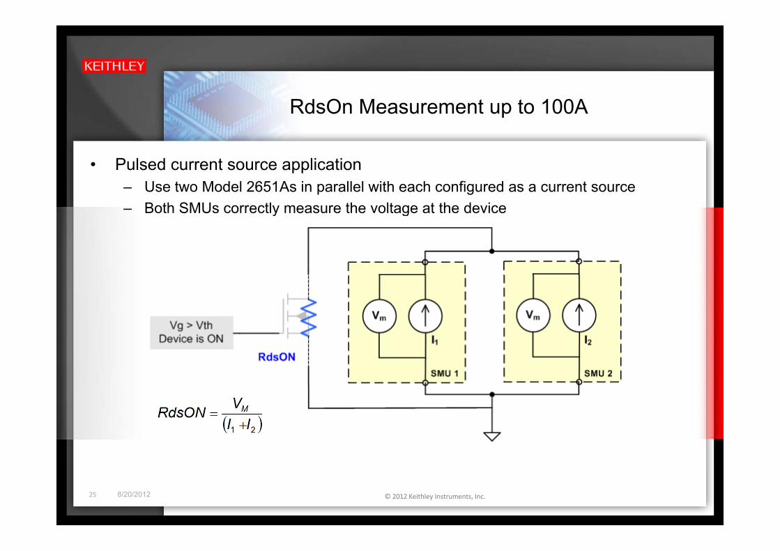
RdsOn Measurement up to 100A
• Pulsed current source application– Use two Model 2651As in parallel with each configured as a current source– Both SMUs correctly measure the voltage at the deviceBoth SMUs correctly measure the voltage at the device
25 8/20/2012 © 2012 Keithley Instruments, Inc.
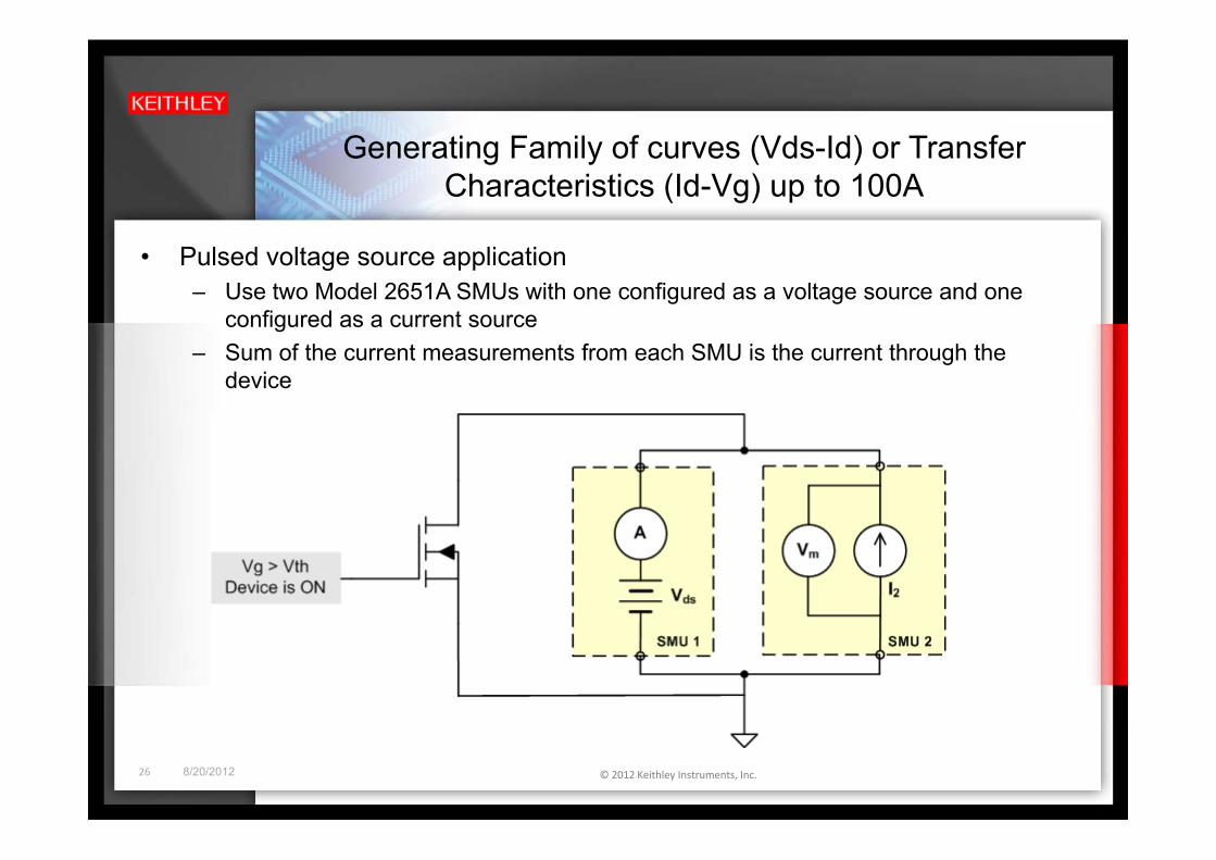
G ti F il f (Vd Id) T fGenerating Family of curves (Vds-Id) or Transfer Characteristics (Id-Vg) up to 100A
• Pulsed voltage source application– Use two Model 2651A SMUs with one configured as a voltage source and one
configured as a current source – Sum of the current measurements from each SMU is the current through the
device
26 8/20/2012 © 2012 Keithley Instruments, Inc.

Off-State Characterization
• Commonly performed at DC to achieve high accuracy leakage measurements
– Very low leakage measurement y gcapability required for new wide bandgap technologies (GaN, SiC)
• Test equipment must be capable of generating high voltages and measuring low currents
• Variety of tests dictates both voltage and current source control
27 8/20/2012 © 2012 Keithley Instruments, Inc.
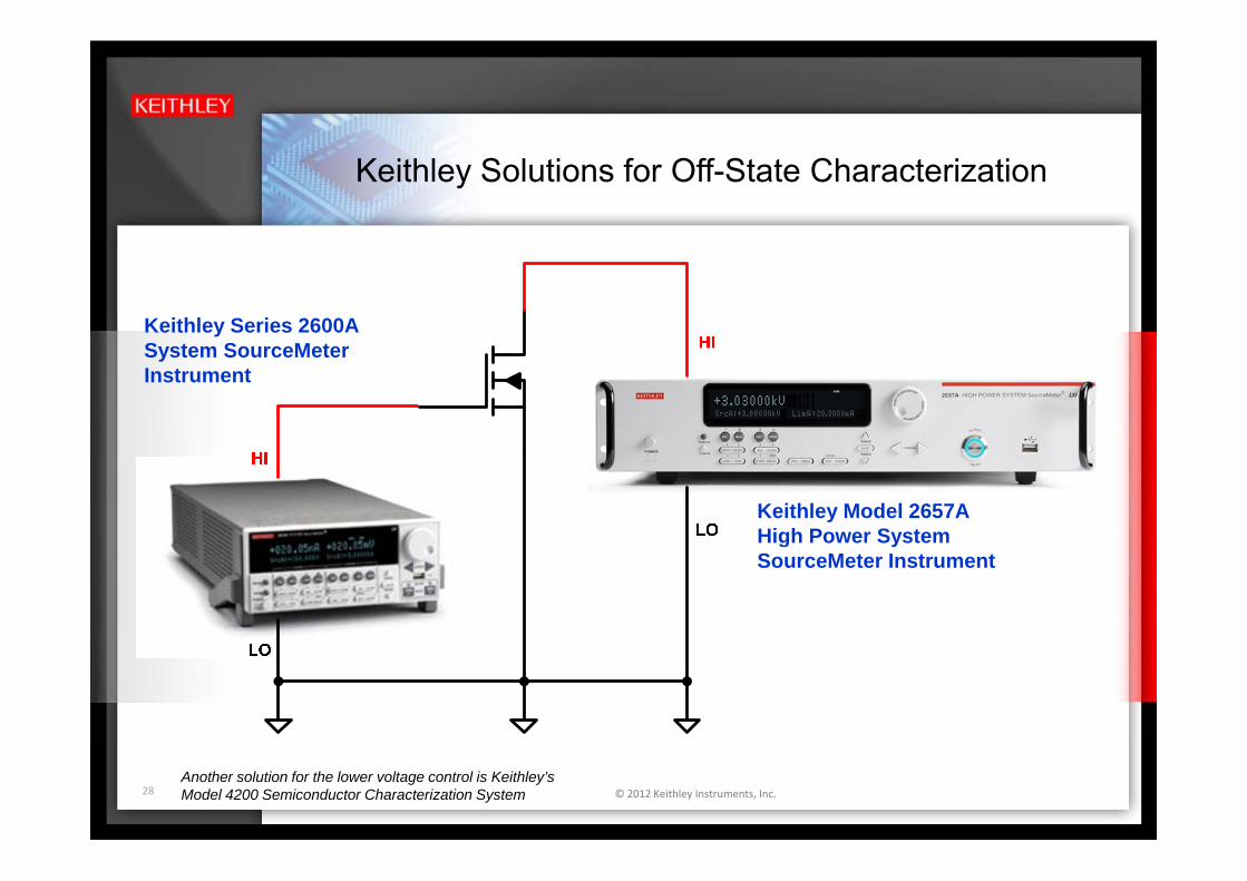
Keithley Solutions for Off-State Characterization
Keithley Series 2600A System SourceMeter Instrument
Keithley Model 2657A High Power SystemHigh Power System SourceMeter Instrument
28 8/20/2012 © 2012 Keithley Instruments, Inc.Another solution for the lower voltage control is Keithley’s Model 4200 Semiconductor Characterization System

Common Considerations for Off-State Characterization
1. Safetya) Personnelb) Instrumentationb) Instrumentationc) Device
2 System capacitance and settling time2. System capacitance and settling time
3. Cabling and connections to achieve optimal low current measurements
29 8/20/2012 © 2012 Keithley Instruments, Inc.
Protecting yourself and others
• Protect operators from hazardous voltage using interlocks and safety enclosures
– Never defeat the interlock!– Ensure that all instruments capable of generating hazardous voltages are disabled
whenever a user attempts to access the DUT. • Ensure that all conductive surfaces that are accessible to the operator are p
properly grounded to protective earth (safety ground) • In some test systems, the measurement common is floating and can float to
hazardous voltages. In such cases, you must take high voltage precautions athazardous voltages. In such cases, you must take high voltage precautions at all terminals.
30 8/20/2012 © 2012 Keithley Instruments, Inc.
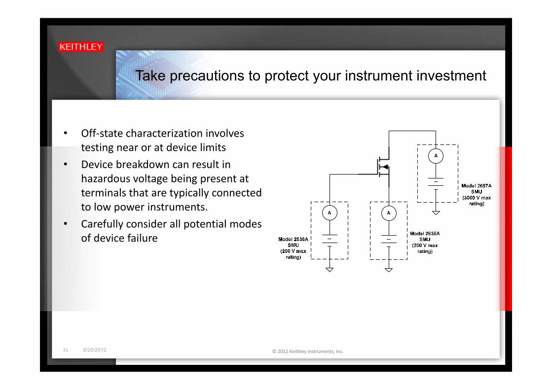
Take precautions to protect your instrument investment
• Off‐state characterization involves testing near or at device limitstesting near or at device limits
• Device breakdown can result in hazardous voltage being present at terminals that are typically connectedterminals that are typically connected to low power instruments.
• Carefully consider all potential modes of device failureof device failure
31 8/20/2012 © 2012 Keithley Instruments, Inc.
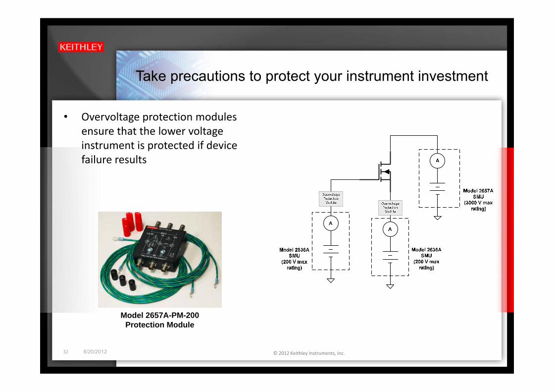
Take precautions to protect your instrument investment
• Overvoltage protection modules ensure that the lower voltage instrument is protected if device failure results
Model 2657A-PM-200 Protection Module
32 8/20/2012 © 2012 Keithley Instruments, Inc.
Take precautions to protect your device
• Off-state characterization typically involves testing device at or beyond device limits. Non-destructive testing is preferred
• Unlike curve tracers and power supplies, Keithley SourceMeter instrumentsUnlike curve tracers and power supplies, Keithley SourceMeter instruments include built-in programmable features to precisely and quickly limit the maximum voltage and current to the device
– As with any protection device (e.g. fuse), the SMU’s limit control has a finiteAs with any protection device (e.g. fuse), the SMU s limit control has a finite response time (tens to hundreds of microseconds)
– Some high speed wide bandgap technology devices have extremely fast and hard breakdown
• Device impedance may change 5-7 orders of magnitude– If the device breaks down faster than SMU has time to respond, then the current
into the device may be higher than the programmed current limit
33 8/20/2012 © 2012 Keithley Instruments, Inc.
Take precautions to protect your device
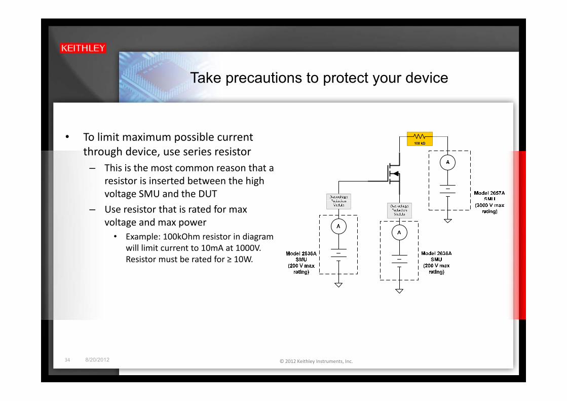
• To limit maximum possible current through device, use series resistorthrough device, use series resistor
– This is the most common reason that a resistor is inserted between the high voltage SMU and the DUT
– Use resistor that is rated for max voltage and max power
• Example: 100kOhm resistor in diagram ill li it t t 10 A t 1000Vwill limit current to 10mA at 1000V.
Resistor must be rated for ≥ 10W.
34 8/20/2012 © 2012 Keithley Instruments, Inc.
K E I T H L E Y C O N F I D E N T I A L – P R O P R I E T A R Y
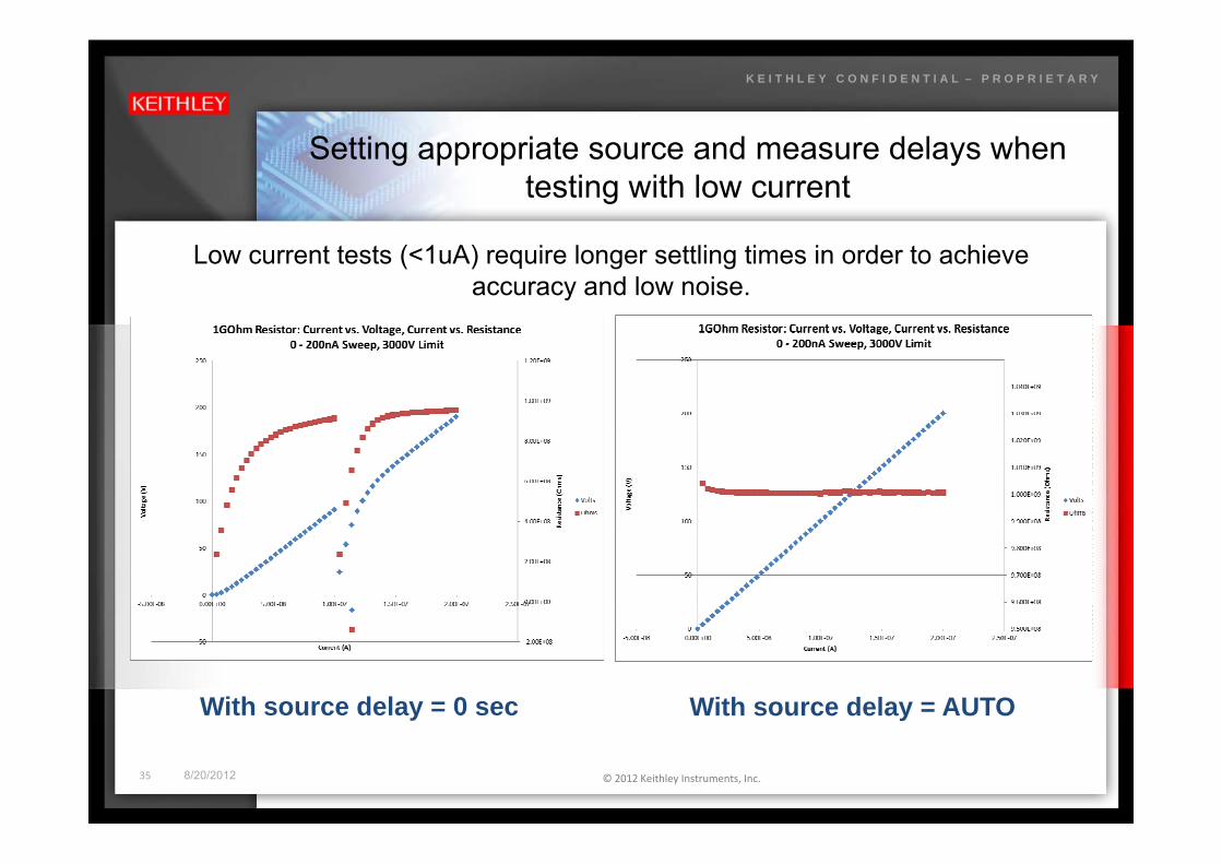
S tti i t d d l hSetting appropriate source and measure delays when testing with low current
Low current tests (<1uA) require longer settling times in order to achieve accuracy and low noise.
With source delay = 0 sec With source delay = AUTO
35 8/20/2012 © 2012 Keithley Instruments, Inc.
Account for System Capacitance and Settling Time
• Source and measure delays need to account for time to charge system capacitance
– This is especially important in prober applications. p y p p pp– Vertical devices require high voltage through chuck.
• Size of chuck and length of cabling results in large capacitance at this terminal
• Capacitive charging times determine the minimum effective pulse width for p g g pthe high voltage instrument
• Use high enough current limit to charge capacitance of system quickly
36 8/20/2012 © 2012 Keithley Instruments, Inc.
K E I T H L E Y C O N F I D E N T I A L – P R O P R I E T A R Y
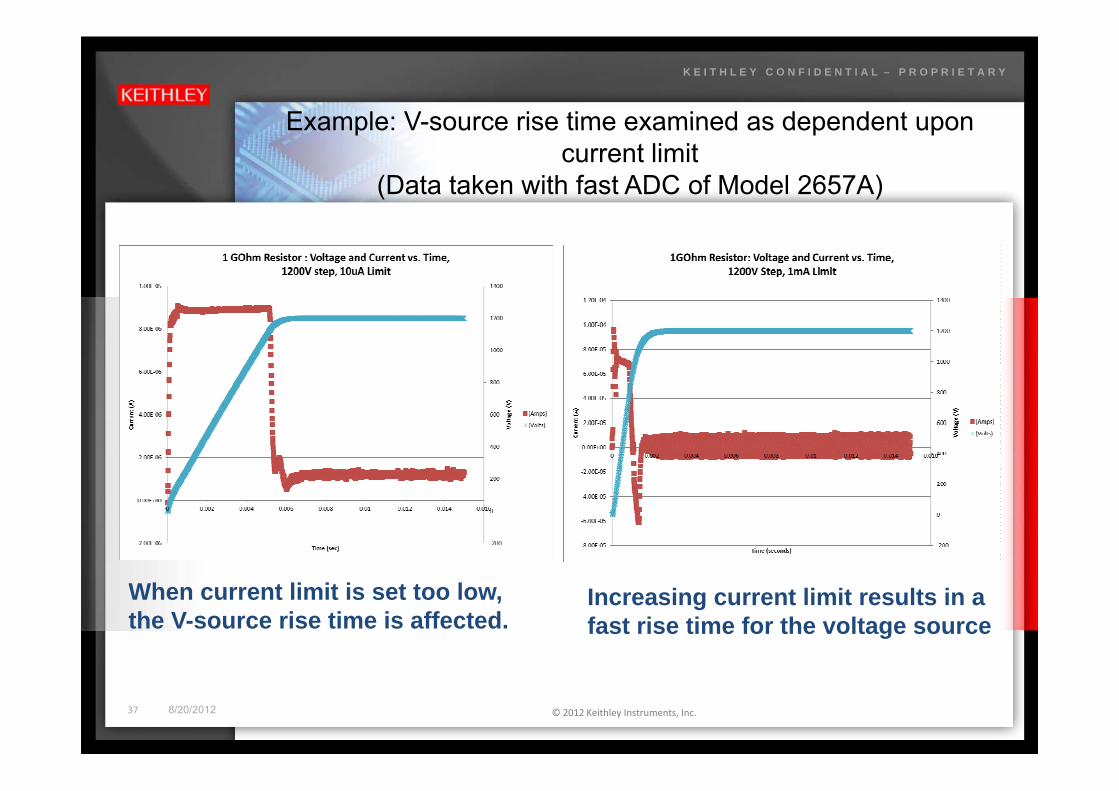
Example: V-source rise time examined as dependent uponExample: V source rise time examined as dependent upon current limit
(Data taken with fast ADC of Model 2657A)
When current limit is set too low, the V-source rise time is affected.
Increasing current limit results in a fast rise time for the voltage source
37 8/20/2012 © 2012 Keithley Instruments, Inc.
K E I T H L E Y C O N F I D E N T I A L – P R O P R I E T A R Y
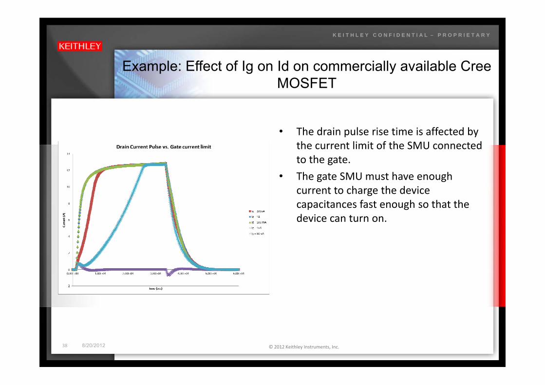
E l Eff t f I Id i ll il bl CExample: Effect of Ig on Id on commercially available Cree MOSFET
• The drain pulse rise time is affected by the current limit of the SMU connectedthe current limit of the SMU connected to the gate.
• The gate SMU must have enough current to charge the devicecurrent to charge the device capacitances fast enough so that the device can turn on.
38 8/20/2012 © 2012 Keithley Instruments, Inc.

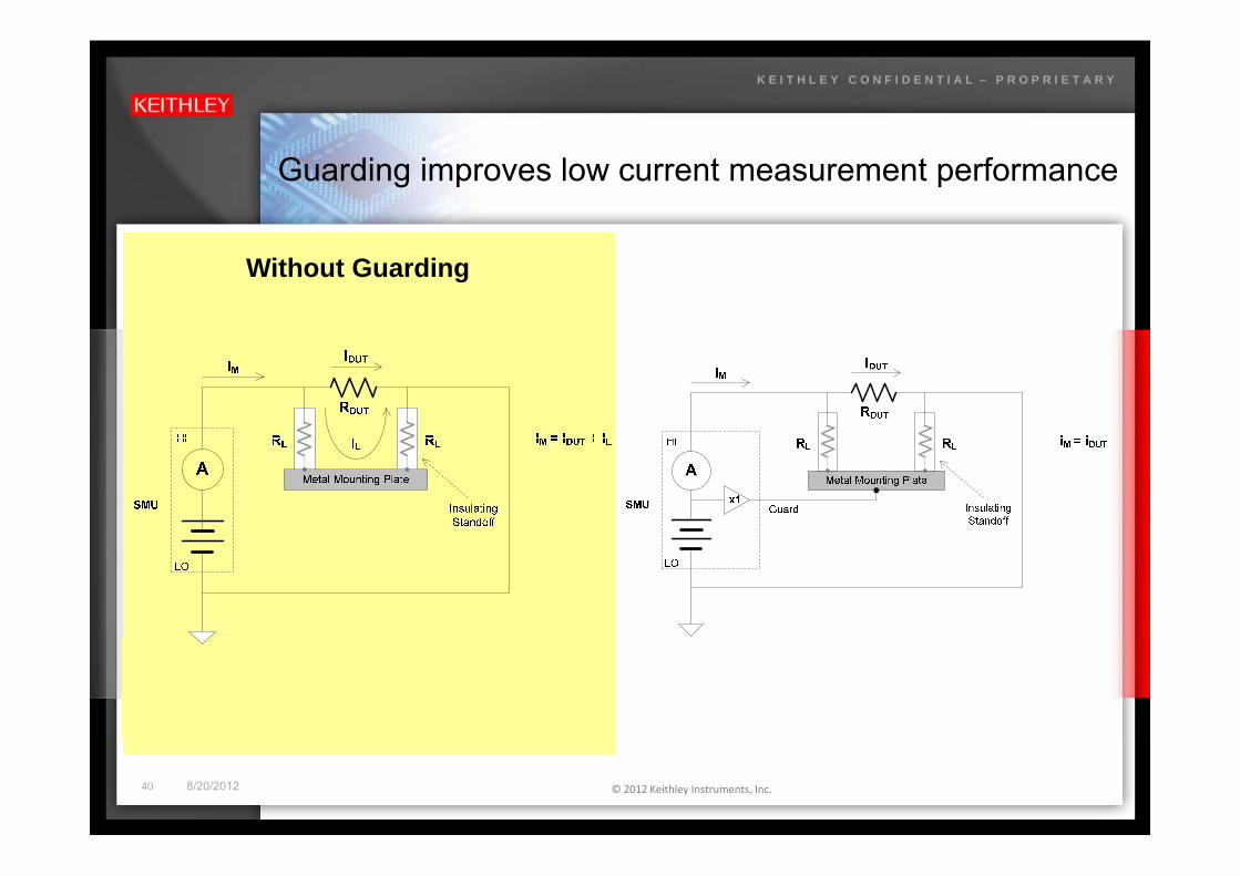
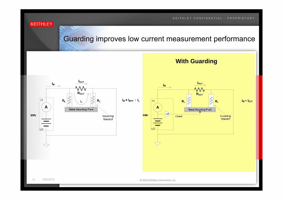
Use guarding to reduce system capacitive charge time
• Capacitance spec of a typical triaxial cable is 40pF / foot. This can result in several hundreds of pF for a 2-3m cable
• Guard is at the same potential as the HI terminal– Use triaxial cabling to carry guard and protect users from electric shock
39 8/20/2012 © 2012 Keithley Instruments, Inc.
• Use guarding to eliminate need to charge cable capacitance
K E I T H L E Y C O N F I D E N T I A L – P R O P R I E T A R Y
Guarding improves low current measurement performance
Without Guarding
40 8/20/2012 © 2012 Keithley Instruments, Inc.
K E I T H L E Y C O N F I D E N T I A L – P R O P R I E T A R Y
Guarding improves low current measurement performance
With Guarding
41 8/20/2012 © 2012 Keithley Instruments, Inc.

K ithl M d l 2651A Hi h PKeithley Model 2651A High Power System SourceMeter Instrument
• 200 Watts of DC Power
• Up to 2000 Watts of pulsed power
• Single unit capable of up to 50A at 40V• Single unit capable of up to 50A at 40V pulse
• Two units can be combined to generate 100A pulsesgenerate 100A pulses
– <1µs multi‐unit synchronization
• Flexible digital I/O for triggering other i t t tiinstrumentation
• Includes separate integrating and high speed ADCs for both voltage and current
– User‐selectable ADC allows use to achieve desired balance in speed and accuracy
42 8/20/2012 © 2012 Keithley Instruments, Inc.
accuracy

K ithl M d l 2657A Hi h P S t S M tKeithley Model 2657A High Power System SourceMeter Instrument
• Up to 180 Watts of DC Power• Continues Keithley’s legacy of high
voltage products that have beenvoltage products that have been utilized for many years in high voltage testing of semiconductors
– 237237– 2410
• Low current measurement• Conditioned for production or• Conditioned for production or
characterization environments: TSP, digital I/O interfaces, can be integrated into dedicated systemsintegrated into dedicated systems as well as used for benchtop characterization systems
43 8/20/2012 © 2012 Keithley Instruments, Inc.

For More information
• Building and configuring systems for power semiconductor device testing– App Note: Creating Multi-SMU Systems with High Power System SourceMeter
Instruments– Website: http://www.keithley.com/promo/lp/high-power-semi/p y p p g p
• Combining SMUs in parallel for testing higher current devices– App Note: Testing to 100 A by Combining Keithley Model 2651A High Power SMU
Instruments• Validating system using high speed ADC of Series 2650A instruments• Validating system using high speed ADC of Series 2650A instruments
– App Note: Measuring Pulsed Waveforms with the High Speed Analog-to-Digital Converter in the Model 2651A High Power System SourceMeter Instruments
• Understanding challenges of low current source and measurement and optimizing the setup:the setup:
– Low Level Measurements Handbook, 6th Edition• For help with application-specific or test-specific questions
– Keithley Web Forums: http://forum.keithley.com• Daily monitored by factory and field applications engineers
– Your local Keithley Field Applications Engineer• Contact information for worldwide sales offices available at http://www.keithley.com
44 8/20/2012 © 2012 Keithley Instruments, Inc.

References
• Keithley Application Note #3163 Creating Multi-SMU Systems with High Power System SourceMeter Instruments
• Keithley’s Low Level Measurements Handbook, 6th Edition• Fairchild Semiconductor Application Bulletin AB-9 “Suppressing MOSFET Gate Ringing
in Converters: Selection of a Gate Resistor”. Available from http://www.fairchildsemi.comAd d P T h l A li ti N t APT 0402 R A “Eli i ti P iti• Advanced Power Technology Application Note APT-0402 Rev. A “Eliminating Parasitic Oscillation Between Parallel MOSFETs” by Jonathan Dodge. Available from http://www.microsemi.com
45 8/20/2012 © 2012 Keithley Instruments, Inc.

K ithl Hi h P S tKeithley High Power System SourceMeter SMU Instruments
Model 2657A High Voltage SMU Instrument
Unmatched Performance for Testing Higher Power Devices
g g•Up to 3,000V and up to 180W of power•1fA resolutionModel 2651A High Current SMU InstrumentModel 2651A High Current SMU Instrument•Up to 50A (or 100A with 2 units) and up to 2000W pulse / 200W DC power•1pA resolution1pA resolution
46 8/20/2012 © 2012 Keithley Instruments, Inc.

Contact and Q&A
全国免费电话 800 810 1334 400 650 1334全国免费电话: 800-810-1334, 400-650-1334吉时利(北京)测量仪器有限公司:
北京市朝阳区霄云路 36 号国航大厦 303 - 308 室邮 编: 100027
全国免费电话: 800-810-1334, 400-650-1334 电 话: +86-10-84475556传 真: +86-10-82255018
电子邮件: [email protected]@ y
上海代表处:上海市徐汇区宜山路900号C楼7楼
电话:021-33970966 电子邮件: [email protected]
深圳代表处:深圳市福田区南园路68号上步大厦21层H室
电话: +86-755-8304 2397传真: +86-755-8246 1539
电子邮件: [email protected]
47 8/20/2012 © 2012 Keithley Instruments, Inc.


![Development of novel micro-fabricated ion traps€¦ · Oneofthemostpromisingsystemsforbuildingaquantumcomputeristheuseoftrapped ions as qubits [13,14]. Paul traps can confine chains](https://img.pdfslide.tips/doc/110x75/5f37f6fd8b0b1926485b98a6/development-of-novel-micro-fabricated-ion-traps-oneofthemostpromisingsystemsforbuildingaquantumcomputeristheuseoftrapped.jpg)


![Grimtooth's Traps Fore c20020824 [75]](https://img.pdfslide.tips/doc/110x75/577c7e9c1a28abe054a1d316/grimtooths-traps-fore-c20020824-75.jpg)