Embed Size (px)
Citation preview

1
TI在ZYNQ系统设计中的电源和高速信号接口解决方案安富利电子科技

2
Agenda
2
1. ZYNQ产品系列以及应用市场介绍2. ZYNQ对电源的要求以及TI电源设计方案3.在工业自动化应用中为ZYNQ选择合适的高速接口

3 3
ZYNQ产品系列以及应用市场介绍-Zhao HongLang

4
Xilinx Product Portfolio
5
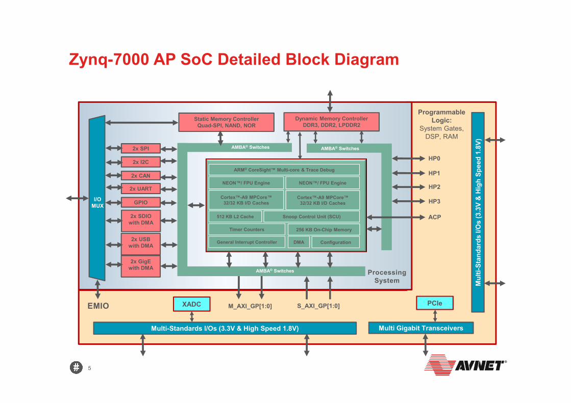
Zynq-7000 AP SoC Detailed Block Diagram
2x GigEwith DMA
2x USBwith DMA
2x SDIOwith DMA
Static Memory ControllerQuad-SPI, NAND, NOR
Dynamic Memory ControllerDDR3, DDR2, LPDDR2
AMBA® Switches
XADC PCIe
Multi-Standards I/Os (3.3V & High Speed 1.8V)
Multi-Sta
ndard
s I/O
s (3.3
V &
Hig
h S
peed 1
.8V)
Multi Gigabit Transceivers
I/OMUX
MI
O
ARM® CoreSight™ Multi-core & Trace Debug
512 KB L2 Cache
NEON™/ FPU Engine
Cortex™-A9 MPCore™32/32 KB I/D Caches
NEON™/ FPU Engine
Cortex™-A9 MPCore™32/32 KB I/D Caches
Snoop Control Unit (SCU)
Timer Counters 256 KB On-Chip Memory
General Interrupt Controller DMA Configuration
2x SPI
2x I2C
2x CAN
2x UART
GPIO
Processing System
AMBA® Switches
AMBA® Switches
AMBA® Switches
EMIO
HP0
HP1
HP2
HP3
ACP
M_AXI_GP[1:0] S_AXI_GP[1:0]
ProgrammableLogic:
System Gates,
DSP, RAM

6
Extensive OS, Middleware, Stacks, Accelerators & IP
• Broad Ecosystem Support
• All major independent OS
• Most up-to-date Linux
support
• Support for SMP & AMP
• OS/RTOS + bare metal
• OS + RTOS
• Xilinx Eclipse based SDK
• Advance profiling &
performance analysis
• Cross trigger debug
• Heterogeneous processor
debug

7
Largest Portfolio of SW & HW Design Tools, SoMs, Design Kits & Reference designs
• Wide distribution of Zynq®-7000 All Programmable SoC based boards/kits
• 17,000+ boards/kits shipped between Xilinx and Avnet
• 25+ Development Boards and SoM’s from Xilinx and its partners
• Application & Market Specific Boards

8
Target Markets and Applications of Xilinx Zynq-7000
• Industry Control• Motor Control
• Servo
• PLC
• Robotics
• Motion Control
• Factory Automation
• >
• Vision
• Machine Vision
• Smart Camera
• IP Camera
• >
• Medical
• CT/MRI/PET
• Ultrasound
• X-Ray
• Endoscope
• >
• Smart Grid
• Power Automation
• Power Monitor
• Relay-Protection
• PQMs
• >
• ADAS• LDW
• 3D Surround View
• Blind Spot Detection
• Intelligent Speed Control
• Pedestrian Detection
• Traffic Sign Recognition
• >
• Consumer
• UAV
• VR/AR
• >
• Wired & Data Center• OTN
• Core Router & Switcher
• Cable Access
• >
• DC Compute (HPC)
• DC Storage
• Networking
• Wireless
• GPS Receiver
• Interphone
• >

9
Powered by Xilinx: Zynq-7000 Success Storieshttp://www.xilinx.com/about/xilinx-go/powered-by-xilinx.html

10
Zynq-7000 Device Portfolio Summary
Zynq-7000 AP SoC
DevicesZ-7010 Z-7015 Z-7020 Z-7030 Z-7035 Z-7045 Z-7100
Pro
cessin
g S
yste
m
Processor Core Dual ARM® Cortex™-A9 MPCore™
Processor Extensions NEON™ & Single / Double Precision Floating Point
Max Frequency 866 MHz Up to 1 GHz
Memory L1 Cache 32KB I / D, L2 Cache 512KB, on-chip Memory 256KB
External Memory Support DDR3, DDR3L, DDR2, LPDDR2,2x QSPI, NAND, NOR
Peripherals2x USB 2.0 (OTG), 2x Tri-mode Gigabit Ethernet,
2x SD/SDIO, 2x UART, 2x CAN 2.0B, 2x I2C, 2x SPI, 4x 32b GPIO
Pro
gra
mm
able
Logic
Approximate ASIC Gates~430K
(28k LC)
~1.1M
(74k LC)
~1.3M
(85k LC)
~1.9M
(125k LC)
~4.1M
(275k LC)
~5.2M
(350k LC)
~6.6M
(444kLC)
Block RAM 240KB 380KB 560KB 1,060KB 2,000KB 2,180KB 3,020KB
Peak DSP Performance
(Symmetric FIR)100 GMACS 200GMACS 276 GMACS 593 GMACS
1334
GMACS1334 GMACS 2662 GMACS
PCI Express®
(Root Complex or Endpoint)- Gen2 x4 - Gen2 x4 Gen2 x8
Agile Mixed Signal (XADC) 2x 12bit 1Msps A/D Converter
I/O
Processor System IO 130
Multi Standards 3.3V IO 100 150 200 100 212 212 250
Multi Standards High
Performance 1.8V IO - - - 150 150 150 150
Multi Gigabit Transceivers - 4 - 4 16 16 16

11 11
ZYNQ对电源的要求以及TI电源设计方案-Vincent Wei

12
ZYNQ7000系列电源要求
SymbolSymbolSymbolSymbol DescriptionDescriptionDescriptionDescription Nominal ValueNominal ValueNominal ValueNominal Value Tolerance(%)Tolerance(%)Tolerance(%)Tolerance(%)VCCPINT PS Internal logic supply voltage 1.0V 5%VCCPAUX PS Auxiliary supply voltage 1.8V 5%VCCPLL PS PLL supply voltage 1.8V 5%VCCO_PS PS output supply voltage for IO banks 1.3V,1.8V
VCCINT PL Internal logic supply voltage(Core Supply) 1.0V 5%VCCAUX PL Auxiliary supply voltage 1.8V 5%VCCO PL output supply voltage for IO banks 1.14-3.465VVCCBRAM PL supply voltage for block RAM memory 1.0V 5%
VMGTVACC Analog supply voltage for GTP transceiver circuits 1.0V 3%VMGTVATT Analog supply voltage for GTP transceiver termination circuits 1.2V 2.5%
Processing System(PS)Processing System(PS)Processing System(PS)Processing System(PS)
Programmable Logic(PL)Programmable Logic(PL)Programmable Logic(PL)Programmable Logic(PL)
GTP Transceiver(XC7Z015 Only)GTP Transceiver(XC7Z015 Only)GTP Transceiver(XC7Z015 Only)GTP Transceiver(XC7Z015 Only)

13
VCCINT VCCBRAM VCCAUX VCCO
VCCPINTVCCPAUXVCCPLL
VCCO_PS
VCCINTVMGTVACC
VMGTVATT
Logic Sequence
Processor Sequence
Transceiver Sequence
ZYNQ7000系列电源时序要求
Power Sequence

14
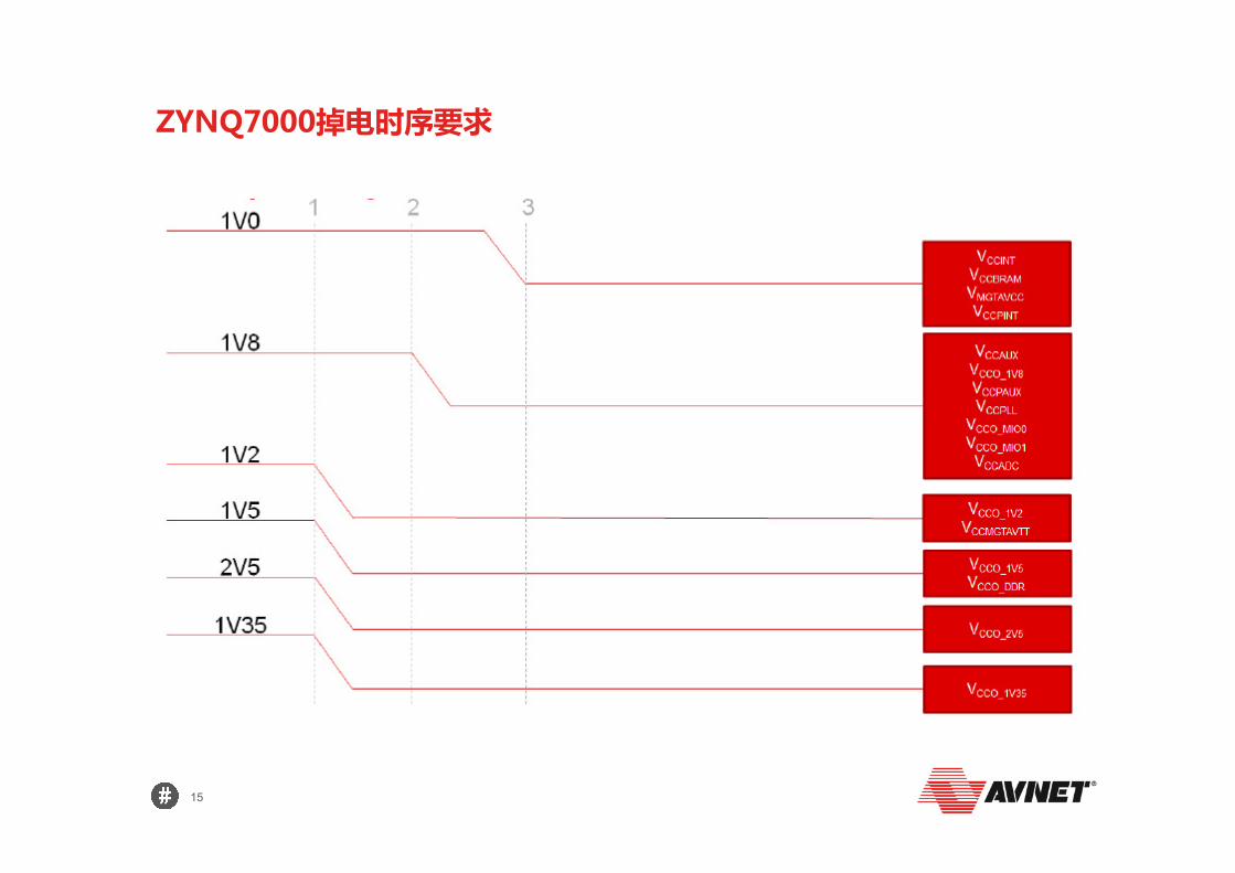
ZYNQ7000上电时序要求
15
ZYNQ7000掉电时序要求

16
12V
TLV62130
1.0V/3A VCCINT
VCCPINT
VCCBRAMTLV62130
1.8V/3AVCCO
VCCPAUX
VCCODDR
VCCO-PL
TLV621301.5V/3A
VCCODDR
TLV621303.3V/3A VCCO_PL
VCCODDR
1
2
3
4
12V电源分离DC-DC供电方案-1 (ZYNQ7010)

17
TLV62130:3 .. 17V VIN, 3A, 3MHz Step-Down Converters in 3x3mm QFN
• General Purpose POL
• Solid State Disk Drives
• Embedded and mobile Computing
• Industrial applications
• High VIN step down converter with small solution size
• 12V @ 3.3V / 3A utilizing a 1uH inductor
• DCS-ControlTM regulation is fast and accurate
• Low quiescent current and selectable switching frequency
for high efficiency
• VFB control allows current source applications
• High Efficiency Step Down Converter with DCS-ControlTM
• VIN range from 3 to 17V
• Adjustable VOUT from 0.9 to 6.0V
• Fixed VOUT options: 1.8V, 3.3V, 5.0V
• Output current up to: 3A (TPS62130)
• Seamless transition to Power Save Mode
• Pin-selectable switching frequency (full, half)
• 100% Duty Cycle Mode
• Programmable Soft Start and Tracking
• Quiescent current of 17uA (typ.)
• Power Good
DEF Pin Selectable Output Voltage
FSW Pin Selectable Switching Frequency
Cstart Adjustable Startup
TR FB Voltage Control
TLV62130EVM

18
VCCINTMGTAVCC
VCCAUXVCCO_MIO0/1
VCCO_1.2V
VCCPLL
5V电源集成供电方案(ZYNQ7010)
BUCK
LP8758
5V
1.0V/4A
1.8V/4A
1.5V/4A
3.3V/4A
VCCINT
VCCPINT
VCCBRAM
VCCO
VCCPAUX
VCCODDR
VCCO-PL
VCCODDR
VCCO_PL
VCCODDR
19
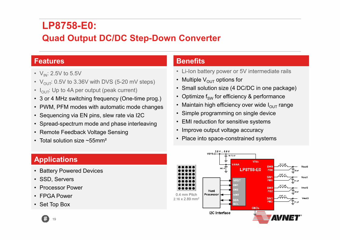
LP8758-E0:Quad Output DC/DC Step-Down Converter
• 19• VIN: 2.5V to 5.5V
• VOUT: 0.5V to 3.36V with DVS (5-20 mV steps)
• IOUT: Up to 4A per output (peak current)
• 3 or 4 MHz switching frequency (One-time prog.)
• PWM, PFM modes with automatic mode changes
• Sequencing via EN pins, slew rate via I2C
• Spread-spectrum mode and phase interleaving
• Remote Feedback Voltage Sensing
• Total solution size ~55mm²
Features
• Li-Ion battery power or 5V intermediate rails
• Multiple VOUT options for
• Small solution size (4 DC/DC in one package)
• Optimize fSW for efficiency & performance
• Maintain high efficiency over wide IOUT range
• Simple programming on single device
• EMI reduction for sensitive systems
• Improve output voltage accuracy
• Place into space-constrained systems
Benefits
• Battery Powered Devices
• SSD, Servers
• Processor Power
• FPGA Power
• Set Top Box
Applications
0.4 mm Pitch
2.16 x 2.89 mm2

20
12V
TLV62130
1.0V/14A VCCINT
VCCPINT
VCCBRAMTPS53319
1.8V/3A VCCO
VCCPAUX
VCCO-PL
TLV621301.5V/3A
VCCODDR
TLV621303.3V/3A
VCCO
1
2
3
4
12V电源分离DC-DC供电方案-2 (ZYNQ7020)

21
• Conversion Input Voltage Range: 3V to 15V• VDD Input Voltage Range: 4.5V to 25V• Output Voltage Range: 0.6V to 5.5V• Built in LDO• D-CAPTM Mode Control Topology
• Switching Frequency from 250k to 1MHz with External
• PowerStack™ packaging technology
• Selectable Auto-Skip or PWM-Only Operation• 0.6V, 1% Reference Accuracy• Remote Sense Support• Internal Soft-Start with Selectable SS Time• OVP, UVP, UVLO, OTP, ENABLE, PGOOD• Pin-to-pin compatible with TPS53355 (30A version)
• Single IC can convert from 3.3V, 5V, and 12V bus rails• Single supply operation from 4.5V to 25V• Supports ASIC core, I/O, and DDR core regulation• No external IC bias voltage required• Only 4x100uF MLCCs needed for 20A load transient
Eliminates 5-6 loop compensation components vs. Voltage Mode control ($0.03-$0.05 BOM cost savings)
• High Fsw enables total power supply area of <1.3in2
• 90% Efficiency at 20A Out @ 500KHz57°C maximum case temperature with no air flow
• 82% Efficiency at light load (<100mA)• High Accuracy Output Voltage Regulation within 1%• Improved System Voltage Accuracy• Flexible design; Eliminates one (1) Soft Start
capacitor• Complete System Protection, Power Sequencing• Design flexibility, Time-To-Market reduction
• Notebook Computers• Server and Desktop Computers• Telecommunication Equipments
TPS5335320A Step-down Integrated FET Converter

22
12V
TLV62130
1.0V/14A VCCINT
VCCPINT
VCCBRAMTPS53319
1.8V/3A VCCO
VCCPAUX
VCCO-PL
TLV621301.5V/3A
VCCODDR
TLV621303.3V/3A
VCCO
1
2
3
4
12V电源分离DC-DC供电方案-3 (ZYNQ7015)
TPS7A7100
TPS7A7100
1.0V/1A
1.2V/1A
VMGTVACC
VMGTVATT

23
• Factory EEPROM programmable VOUT
• Wide Vin range 1.5V – 7.0V(TBD)
• TPS737xx/796xx Similar Pinout
• 2% Accuracy
• Low Output Noise/ High PSRR
– 30mVRMS(TBD)
– PSRR 55dB @ 1kHz(TBD)
• Programmable SoftStart
• Power Good Output
• 20-Pin 5x5mm RGW (QFN) Package(TBD)
• 10-Pin 3x3mm DRC (SON 10) Package
• Wireless Infrastructure (Tx/Rx, FPGA&DSP)
• RF: 5V components, VCOs, Receivers, ADCs
• SetTopBox (Amp,AD/DA,FPGA&DSP)
• Wireless LAN, Bluetooth
• PC & Printers
• Audio and Visual
• Quickly sample/release new custom versions
• Applications requiring VIN > 5.5V & VIN < 2.0V
• Easy upgrade path for existing designs
• Applications requiring stable Vout
• RF/Audio Noise Sensitive Applications
• Reduces in-rush current
• Application requiring sequencing
• Enhanced thermal performance
• 65% smaller than 5 x 5mm QFN package
Device VIN IOUT VDO IQ Package
TPS7A71xx 1.5 – 7.0V 1A 100mV 2mA RGW, DRC
TPS7A72xx 1.5 – 7.0V 2A 200mV 2.5mA RGW, DRC
TPS7A73xx 1.5 – 7.0V 3A 300mV 3mA RGW, DRC
RGW(QFN)
5mm x 5mm
(Top View)
VINVOUT
VIN
VIN
VINVOUT
VOUT
VOUT
NC
NC
NC
EN
NC
NC
PG
NC
FB
SS
GND
NR
GND
DRC(SON-10)3mm x 3mm
VOUT VIN
VINVOUT
FB
GND
NR
EN
SS
PGGND
(Top View)
TPS7A7100/200/3001A - 3A Wide VIN LDO with SS & PG
23
Power for VCCx_GXB transceiver requirements
24 24
在工业自动化应用中为ZYNQ选择合适的高速接口-Liu HongRui

25 25
FPGA SSD
SATA/PCIe
Serializer Deserializer
Serializer Deserializer
Tx
FPGA
Imagin
g
Sensor
BR
Rx
AFE
Factory Automation Block Diagram
Display

26
Factory Automation and Control Device Description Alternate
CMOS SensorDS90LV047A
DS90LV048AQuad Driver/ Receiver LVDS Pair
DS90LV011A
DS90LV012A
(Single Channel)
DisplayDS92LV2421
DS92LV242224-bit, 10-75 MHz Embedded Clock SerDes
DS90CR285
DS90CR286A
(10-65MHz)
CameraDS92LX1621
DS92LX162216-bit, 10-50 MHz Embedded Clock & Control SerDes
DS92LX2121
DS92LX2122
(21-bit)
Storage
DS64BR111 2-channel, 6.4 Gbps Bi-directional RepeaterDS125BR111
(12.5 Gbps)
DS80PCI102 2-channel (x1), PCIe Gen 1/2/3 Repeater/RedriverDS80PCI810
(8 channel)
Hard Drive
FlashDrive
Factory Automation Solutions
TI Information – Selective Disclosure 26

27
Features Benefits
>100 Mbps Switching Rate • Supports high frequency rate with minimal jitter and
noise
Low Power Consumption • Simplifies design
Industrial Temp Range & Low EMI
• Ensures reliability and usability
LVDS
Driver
LVDS
Receiver
Tx Rx
Clock
Control bus
TTL/CMOS TTL/CMOS
27
LVDS Overview- Transceiver/Driver/Receiver

28
Number of Channels
1 2 4 9
DS90LV049 400 Mbps
DS90LV0041 Gbps
DS90LV047A400 Mbps
DS90LV028A400 Mbps
DS90LV018A400 Mbps
DS90LV011A400 Mbps
DS90LV017A600Mbps
DS90LV048A400 Mbps
DS90LV012A400 Mbps
DS9DS911C180Full Duplex200 Mbps
DS91C176Half Duplex200 Mbps
Receiver
Driver
Transceiver
DS92LV090A100 Mbps
Full-Duplex Transceivers
Half-Duplex Transceivers
Drivers
Receivers
DS91M124 100 Mbps
DS91M125100 Mbps
DS90LV027A600 Mbps
DS90LT012AQ-Q1400 Mbps
DS90LV011AQ-Q1400 Mbps
DS90LV027AQ-Q1600 Mbps
DS90LV028AQ-Q1400 Mbps
EXISTING NEW ROADMAP
28
LVDS Portfolio
DS90LV049Q-Q1 400 Mbps
AUTO QUAL
More devices available on ti.com/lvds

29
SerializerApplication
Logic
Timing
Controller
Processor
Deserializer
“OpenLDI”
“LVDS”CSI-2
SerializerApplication
Logic
Processor
Timing Controller
or
Application Logic
LCD Module /
ProcessorDeserializer
RGBParallel
LVCMOS
SerializerApplication
Logic
Application
Logic
Processor Processor
Bridge
RGBParallel
LVCMOS
29
SerDes Overview- Bridge Multiple Interface Standards

30
Receiv
ers
Tra
nsm
itters DS90UH927Q-Q1
24 bit, 5–85 MHz
DS90UH925Q-Q124 bit, 5-85 MHz
DS90UB927Q-Q124 bit, 5–85 MHz
DS90UH928Q-Q124 bit, 5–85 MHz
DS90UH926Q-Q124 bit, 5–85 MHz
DS90UB928Q-Q124 bit, 5–85 MHz
DS90UR907Q-Q124-bit, 5–65 MHz
DS90UR905Q-Q124-bit, 5–65 MHz
DS90UR908Q-Q124-bit, 5–65 MHz
DS90UR906Q-Q124-bit, 5–65 MHz
EXISTING NEW ROADMAP
DS90UB925Q-Q124 bit, 5–85 MHz
DS90UB926Q-Q124 bit, 5–85 MHz
DS90CF38848 bit 40–112MHz
*DS90C38748 bit 32.5–112MHz *DS90C187
48 bit
SISO: 25-105MHz
DIDO: 50-185MHz
*DS90C18528 bit 25-105MHz
DS90UB94x-Q124 bit, 25–170 MHz
DS90UH94x-Q124 bit, 25–170 MHz
DS90UB94x-Q124 bit, 25–170 MHz
DS90UH94x-Q124 bit, 25–170 MHz
SN75LVDS86A-Q121 bit 31–68 MHz
SN75LVDS93A-Q1-40 to 85C
10–135 MHz
DS90CR28528 bit 20-65MHz
DS90CR286A-Q1-40 to 105C
28 bit 20-66MHz
DS90CR286A-Q1-40 to 85C
28 bit 20-66MHz
DS92LV242124 bit 10-75MHz
DS92LV242224 bit 10-75MHz
DS92LV04214 bit 10-75MHz
DS92LV04224 bit 10-75MHz
DS92LV04114 bit 5-50MHz
DS92LV04124 bit 5-50MHz
DS92LV324132 bit 20-85MHz
DS92LV322132 bit 20-50MHz
DS92LV324232 bit 20-85MHz
DS92LV322232 bit 20-50MHz
DS92LV241124 bit 5-50MHz
DS92LV241224 bit 5-50MHz
DS90CR218A21 bit 20-75MHz
DS90CR21721 bit 20-85MHz
30*In consideration for auto qual
DS92LX212221 bit, 10–50 MHz
DS92LX162216 bit, 10–50MHz
DS92LX212121 bit, 10–50 MHz
DS92LX162116 bit, 10–50 MHz
CONCEPT
DS90CR286A24 bit 20–66MHz
SerDes Overview- SerDes Portfolio More devices available on ti.com/lvds

31
Thank You !