Embed Size (px)
Citation preview
Data Sheet, Rev. 1.70, Sep. 2009
TLE 7263EIntegrated HS-CAN, LIN, LDO and HS SwitchSystem Basis Chip
Automot ive Power
Never stop thinking.
Integrated HS-CAN, LIN, LDO and HS SwitchSystem Basis Chip
TLE 7263E
PG-DSO-36-24
1 Overview
Features• Two Low Drop Voltage Regulators• Window watchdog• Standard 16-bit SPI-interface• Supports μController Stop Mode• Sleep Mode (50µA)• VBAT Monitoring and fail-safe output• Overtemperature and short circuit protection• Power on and undervoltage reset generator• High side switch, 150 mA• 4 Monitoring / wake-up inputs• Exposed Pad Package• AEC Qualified• Green (RoHS Compliant) product
HS CAN Transceiver• CAN data transmission rate up to 1 MBaud• Low power mode management• Supports sleep and receive-only modes• Bus wake-up capability via CAN message• Bus pins are short circuit proof to ground and battery voltage
LIN Transceiver• Single-wire transceiver• Transmission rate up to 20 kBaud• Compatible to LIN specification 1.3, 2.0, 2.1 and SAE J2602-2• Very low current consumption in Sleep Mode• Short circuit proof to GND and battery
Type Package MarkingTLE 7263E PG-DSO-36-24
Data Sheet 2 Rev. 1.70, 2009-09-30
TLE 7263E
Overview
Dual-Voltage Regulator• Low-dropout voltage regulator, dual voltage-supply• V1, 150 mA, 5 V ±2% for external devices, e.g. microcontrollers• V2, 150 mA, 5 V ±2% for internal CAN module and external devices.
DescriptionThe TLE 7263E is a monolithic integrated circuit in an enhanced power package. The ICis designed for CAN-LIN gateway applications.To support these applications the TLE 7263E covers smart power functions such as HS-CAN transceiver and LIN transceiver for data transmission, dual low dropout voltageregulator (LDO) for external 5 V supply, and high-side switch as well as a 16-bit SPI(serial peripheral interface) to control and monitor the IC. There is also a windowwatchdog circuit with a reset feature, a fail-safe output, a voltage sensing input and aundervoltage reset feature implemented.The device offer low power modes in order to support modules directly connected to thebattery (KL. 30). A wake-up from the low power mode is possible via a message on thebus or via the bi level sensitive monitoring/wake-up inputs. The integrated High-Sideswitch can also be used to periodically supply an external wake-up circuitry in the lowpower mode, by choosing a special function. The integrated bus transceivers offer areceive-only mode for software diagnosis functions. The IC is designed to withstand the severe conditions of automotive applications.
Data Sheet 3 Rev. 1.70, 2009-09-30
TLE 7263E
Pin Configuration
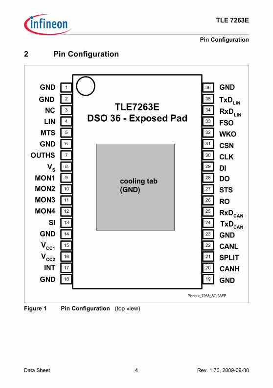
2 Pin Configuration
Figure 1 Pin Configuration (top view)
1
2
3
4
5
6
7
8
9
10
11
12
13
14
15
16
17
18
GND
NCLIN
MON2MON3MON4
SIGNDVCC1
VCC2
INT CANH
36
35
34
33
32
31
30
29
28
27
26
25
24
23
22
21
20
19
GND
RxDLIN
GND
FSOWKOCSNCLK
DOSTSRORxDCAN
TxDCAN
GNDCANLSPLIT
TxDLIN
MTSGND
OUTHSVS
MON1DI
cooling tab(GND)
GND GND
Pinnout_7263_SO-36EP
TLE7263EDSO 36 - Exposed Pad
Data Sheet 4 Rev. 1.70, 2009-09-30
TLE 7263E
Pin Configuration
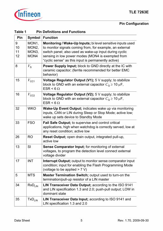
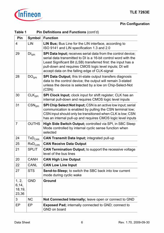
Table 1 Pin Definitions and FunctionsPin Symbol Function
9101112
MON1,MON2,MON3,MON4
Monitoring / Wake-Up Inputs; bi level sensitive inputs used to monitor signals coming from, for example, an external switch panel; also used as wake-up input during cyclic sensing in low power modes (MON4 is exempted from “cyclic sense” as this input is permanently active)
8 VS Power Supply Input; block to GND directly at the IC with ceramic capacitor; (ferrite recommended for better EMC behavior)
15 VCC1 Voltage Regulator Output (V1); 5 V supply; to stabilize block to GND with an external capacitor CQ ≥ 10 μF,ESR < 6 Ω
16 VCC2 Voltage Regulator Output (V2); 5 V supply; to stabilize block to GND with an external capacitor CQ ≥ 10 μF,ESR < 6 Ω
32 WKO Wake-Up Event Output; indicates wake up via monitoring inputs, CAN or LIN during Sleep or Stop Mode; active low; wake up sets device to Standby Mode
33 FSO Fail Safe Output; to supervise and control critical applications, high when watchdog is correctly served, low at any reset condition; active low
26 RO Reset Output; open drain output, integrated pull-up,active low
13 SI Sense Comparator Input; for monitoring of external voltages, to program the detection level connect external voltage divider
17 INT Interrupt Output; output to monitor sense comparator input condition; input for enabling the Flash Programming Mode (voltage to be applied > 7 V)
5 MTS Master Termination Switch; output used to turn-on the termination/pull-up resistor of a LIN master
34 RxDLIN LIN Transceiver Data Output; according to the ISO 9141 and LIN specification 1.3 and 2.0; push-pull output; LOW in dominant state
35 TxDLIN LIN Transceiver Data Input; according to ISO 9141 and LIN specification 1.3 and 2.0
Data Sheet 5 Rev. 1.70, 2009-09-30
TLE 7263E
Pin Configuration
4 LIN LIN Bus; Bus Line for the LIN interface, according to ISO 9141 and LIN specification 1.3 and 2.0
29 DISPI SPI Data Input; receives serial data from the control device; serial data transmitted to DI is a 16-bit control word with the Least Significant Bit (LSB) transferred first: the input has a pull-down and requires CMOS logic level inputs; DI will accept data on the falling edge of CLK-signal
28 DOSPI SPI Data Output; this tri-state output transfers diagnosis data to the control device; the output will remain 3-stated unless the device is selected by a low on Chip-Select-Not (CSN)
30 CLKSPI SPI Clock Input; clock input for shift register; CLK has an internal pull-down and requires CMOS logic level inputs
31 CSNSPI SPI Chip Select Not Input; CSN is an active low input; serial communication is enabled by pulling the CSN terminal low; CSN input should only be transitioned when CLK is low; CSN has an internal pull-up and requires CMOS logic level inputs
7 OUTHS High Side Switch Output; controlled via SPI, in SBC Sleep Mode controlled by internal cyclic sense function when selected
24 TxDCAN CAN Transmit Data Input; integrated pull-up25 RxDCAN CAN Receive Data Output21 SPLIT CAN Termination Output; to support the recessive voltage
level of the bus lines20 CANH CAN High Line Output22 CANL CAN Low Line Input27 STS Send-to-Sleep; to switch the SBC back into low current
mode during cyclic wake1, 2, 6,14,18,19,23,36
GND Ground
3 NC Not Connected Internally; leave open or connect to GNDEP EP Exposed Pad; internally connected to GND; connect to
GND on board
Table 1 Pin Definitions and Functions (cont’d)
Pin Symbol Function
Data Sheet 6 Rev. 1.70, 2009-09-30
TLE 7263E
Block Diagram
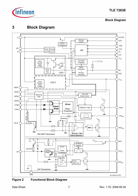
3 Block Diagram
Figure 2 Functional Block Diagram
MON4
BandGap
-+
ResetGenerator
+Window
Watchdog
SPI
DO
DI
CLK
CSN
RO
VCC1
GND
OscillatorTimebase
LDO 1
Receiver
OutputStage
Driver
Temp.-Protection
30 kOhm
LIN ModeControl
TxDLIN
RxDLIN
TxDCAN
LIN
STS
Receiver + BusFailure Detection
OutputStage
Driver
Temp.-Protection
CANH
CANL
+timeout
HS-CANMode Control
RxDCAN
VS
HS-CAN Transceiver
LIN Transceiver
OverCurrent
Overvoltage
Interruptcontrol
OverCurrent
Overvoltage
Vs
SPLIT
Wake-UpLogic
FSO
Early WarningVS SupervisorSI
INT
Drive +Protection
OUTHS
MON2
MON3
Filter /Wake-Up
MUX
VCC1
Diagnosis Logic WKO
VCC1
MTSVS
blockdiagramm7263
VCC2
LDO 2
MON1
VCC1
VCC1
Data Sheet 7 Rev. 1.70, 2009-09-30
TLE 7263E
Features
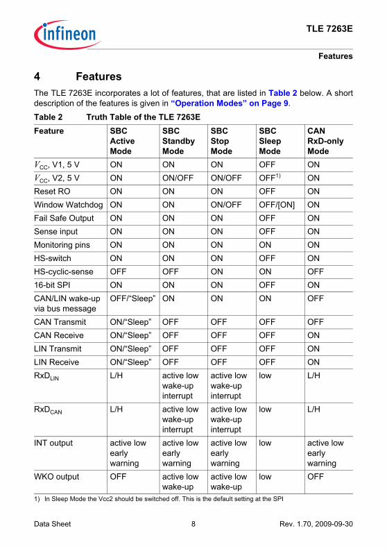
4 FeaturesThe TLE 7263E incorporates a lot of features, that are listed in Table 2 below. A shortdescription of the features is given in “Operation Modes” on Page 9.
Table 2 Truth Table of the TLE 7263EFeature SBC
ActiveMode
SBCStandbyMode
SBCStopMode
SBCSleepMode
CANRxD-onlyMode
VCC, V1, 5 V ON ON ON OFF ONVCC, V2, 5 V ON ON/OFF ON/OFF OFF1)
1) In Sleep Mode the Vcc2 should be switched off. This is the default setting at the SPI
ONReset RO ON ON ON OFF ONWindow Watchdog ON ON ON/OFF OFF/[ON] ONFail Safe Output ON ON ON OFF ONSense input ON ON ON OFF ONMonitoring pins ON ON ON ON ONHS-switch ON ON ON OFF ONHS-cyclic-sense OFF OFF ON ON OFF16-bit SPI ON ON ON OFF ONCAN/LIN wake-upvia bus message
OFF/“Sleep” ON ON ON OFF
CAN Transmit ON/“Sleep” OFF OFF OFF OFFCAN Receive ON/“Sleep” OFF OFF OFF ONLIN Transmit ON/“Sleep” OFF OFF OFF ONLIN Receive ON/“Sleep” OFF OFF OFF ONRxDLIN L/H active low
wake-up interrupt
active low wake-up interrupt
low L/H
RxDCAN L/H active low wake-up interrupt
active low wake-up interrupt
low L/H
INT output active low early warning
active low early warning
active low early warning
low active low early warning
WKO output OFF active low wake-up
active low wake-up
low OFF
Data Sheet 8 Rev. 1.70, 2009-09-30
TLE 7263E
Features
4.1 Operation ModesThis System Basis Chip (SBC) offers five main operation modes that are controlled viathree mode select bits MS1, MS2 and MS3 within the SPI: SBC Active, Standby, Sleepand Stop mode, as well as CAN Receive-Only mode. After powering-up the SBC, itstarts-up in SBC Standby Mode, waiting for the microcontroller to finish its startup andinitialization sequences. From this transition mode the SBC can be switched via SPIcommand into the desired operating mode (The device should not be switched directlyfrom Standby Mode to Sleep or Stop Mode). All modes are selected via SPI bits orcertain operation conditions, e.g. external wake-up events.The SBC Active Mode, that is used in order to transmit and receive CAN and LINmessages, supports two additional sub-modes, “CAN Sleep” and “LIN Sleep”. Duringthese sub-modes the SBC remains its voltage regulators running in order to supplyexternal devices. Also, the line termination of the “sleeping” bus transceiver is turned-offrespectively.During SBC Sleep Mode, the lowest power consumption is achieved, by having its mainvoltage regulator switched-off. As the microcontroller can not be supplied, the integratedwindow watchdog might be disabled in Sleep Mode via SPI bit. However, it can beturned-on for periodically waking-up the system, e.g. ECU, by generating a reset.In case an external microcontroller needs to be supplied with its quiescent current, theSBC Stop Mode can be chosen. In this mode the main voltage regulator remains active.Optionally, the second voltage regulator can be turned-on or off via the SPI prior toentering one of the respective power saving modes. The integrated window watchdogremains active until the microcontroller enters its power saving mode (“Stop Mode”). Thispower saving mode is assumed to be reached once the current consumption is below acertain threshold (see Watchdog current threshold, Table and “Window Watchdog,Reset” on Page 26).In both low power modes the internal bus transceivers, including the line termination, areturned off while the wake-up capabilities via bus message or monitoring pins are stillactive. The SBC offers Sleep and Stop Mode in conjunction with or without the CyclicSense/Wake feature. If the Cyclic Sense/Wake feature is selected, two possible statescan be entered during Sleep/Stop Mode: HS-On and HS-Off (see text and respectivestate diagram).The Cyclic Sense feature can be used to supply an external wake-up circuitryperiodically, and is entered upon activation via SPI command. In cyclic sense HS-Onstate, the High-Side switch is activated for a certain “on-time” and provides supplyvoltage at its OUTHS pin. Within this on-time the SBC starts sampling of themonitoring/wake-up lines. On-time as well as time period are programmable via the SPIcontrol word. A wake-up at the monitoring / wake-up pins during the on-time as well asa message at the CAN or LIN bus lines automatically sets the TLE 7263E into SBCStandby mode, and turns-on the main voltage regulator VCC1. The digital RxDCAN/RxDLINlines, that are monitored by the microcontroller during power saving, are pulled low with
Data Sheet 9 Rev. 1.70, 2009-09-30
TLE 7263E
Features
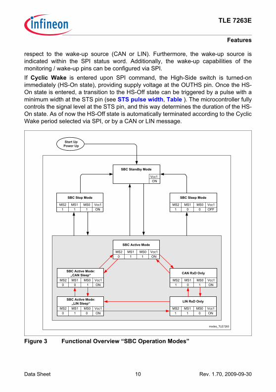
respect to the wake-up source (CAN or LIN). Furthermore, the wake-up source isindicated within the SPI status word. Additionally, the wake-up capabilities of themonitoring / wake-up pins can be configured via SPI. If Cyclic Wake is entered upon SPI command, the High-Side switch is turned-onimmediately (HS-On state), providing supply voltage at the OUTHS pin. Once the HS-On state is entered, a transition to the HS-Off state can be triggered by a pulse with aminimum width at the STS pin (see STS pulse width, Table ). The microcontroller fullycontrols the signal level at the STS pin, and this way determines the duration of the HS-On state. As of now the HS-Off state is automatically terminated according to the CyclicWake period selected via SPI, or by a CAN or LIN message.
Figure 3 Functional Overview “SBC Operation Modes”
Start UpPower Up
SBC Stop Mode
MS2ON
Vcc1MS11 1
MS01
SBC Standby Mode
ONVcc1
modes_TLE7263
SBC Sleep Mode
MS2OFFVcc1MS1
1 0MS0
0
SBC Active Mode
MS2ON
Vcc1MS10 1
MS01
SBC Active Mode:„CAN Sleep“
MS2ON
Vcc1MS10 0
MS01
MS2ON
Vcc1MS10 1
MS00
SBC Active Mode:„LIN Sleep“ LIN RxD Only
MS2ON
Vcc1MS11 1
MS00
CAN RxD Only
MS2ON
Vcc1MS11 0
MS01
Data Sheet 10 Rev. 1.70, 2009-09-30
TLE 7263E
Features
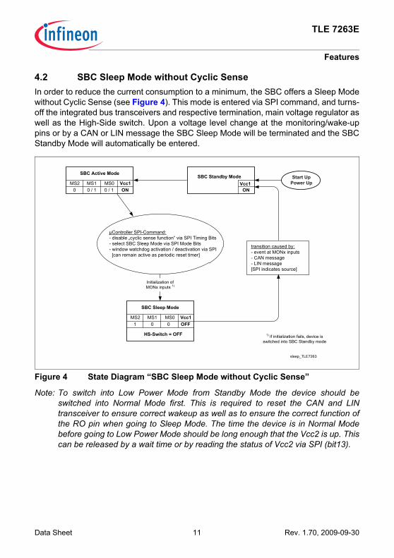
4.2 SBC Sleep Mode without Cyclic SenseIn order to reduce the current consumption to a minimum, the SBC offers a Sleep Modewithout Cyclic Sense (see Figure 4). This mode is entered via SPI command, and turns-off the integrated bus transceivers and respective termination, main voltage regulator aswell as the High-Side switch. Upon a voltage level change at the monitoring/wake-uppins or by a CAN or LIN message the SBC Sleep Mode will be terminated and the SBCStandby Mode will automatically be entered.
Figure 4 State Diagram “SBC Sleep Mode without Cyclic Sense”
Note: To switch into Low Power Mode from Standby Mode the device should beswitched into Normal Mode first. This is required to reset the CAN and LINtransceiver to ensure correct wakeup as well as to ensure the correct function ofthe RO pin when going to Sleep Mode. The time the device is in Normal Modebefore going to Low Power Mode should be long enough that the Vcc2 is up. Thiscan be released by a wait time or by reading the status of Vcc2 via SPI (bit13).
Start UpPower Up
sleep_TLE7263
µController SPI-Command:- disable „cyclic sense function“ via SPI Timing Bits- select SBC Sleep Mode via SPI Mode Bits- window watchdog activation / deactivation via SPI [can remain active as periodic reset timer]
SBC Active Mode
MS2ON
Vcc1MS10 0 / 1
MS00 / 1
transition caused by:- event at MONx inputs- CAN message- LIN message[SPI indicates source]
SBC Sleep Mode
MS2OFFVcc1MS1
1 0MS00
HS-Switch = OFF
Initialization of MONx inputs 1)
1) if initialization fails, device is switched into SBC Standby mode
SBC Standby Mode
ONVcc1
Data Sheet 11 Rev. 1.70, 2009-09-30
TLE 7263E
Features
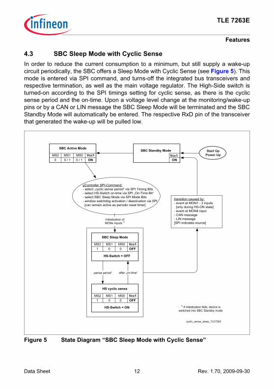
4.3 SBC Sleep Mode with Cyclic SenseIn order to reduce the current consumption to a minimum, but still supply a wake-upcircuit periodically, the SBC offers a Sleep Mode with Cyclic Sense (see Figure 5). Thismode is entered via SPI command, and turns-off the integrated bus transceivers andrespective termination, as well as the main voltage regulator. The High-Side switch isturned-on according to the SPI timings setting for cyclic sense, as there is the cyclicsense period and the on-time. Upon a voltage level change at the monitoring/wake-uppins or by a CAN or LIN message the SBC Sleep Mode will be terminated and the SBCStandby Mode will automatically be entered. The respective RxD pin of the transceiverthat generated the wake-up will be pulled low.
Figure 5 State Diagram “SBC Sleep Mode with Cyclic Sense”
Start UpPower Up
cyclic_sense_sleep_TLE7263
µController SPI-Command:- select „cyclic sense period“ via SPI Timing Bits- select HS-Switch on-time via SPI „On-Time Bit“- select SBC Sleep Mode via SPI Mode Bits- window watchdog activation / deactivation via SPI [can remain active as periodic reset timer]
SBC Active Mode
MS2ON
Vcc1MS10 0 / 1
MS00 / 1
transition caused by:- event at MON1 - 3 inputs [only during HS-ON state]- event at MON4 input- CAN message- LIN message[SPI indicates source]
SBC Sleep Mode
MS2OFFVcc1MS1
1 0MS00
HS-Switch = OFF
HS cyclic sense
MS2OFFVcc1MS1
1 0MS00
HS-Switch = ON
after „on-time“„sense period“
Initialization of MONx inputs 1)
1) if initialization fails, device is switched into SBC Standby mode
SBC Standby Mode
ONVcc1
Data Sheet 12 Rev. 1.70, 2009-09-30
TLE 7263E
Features
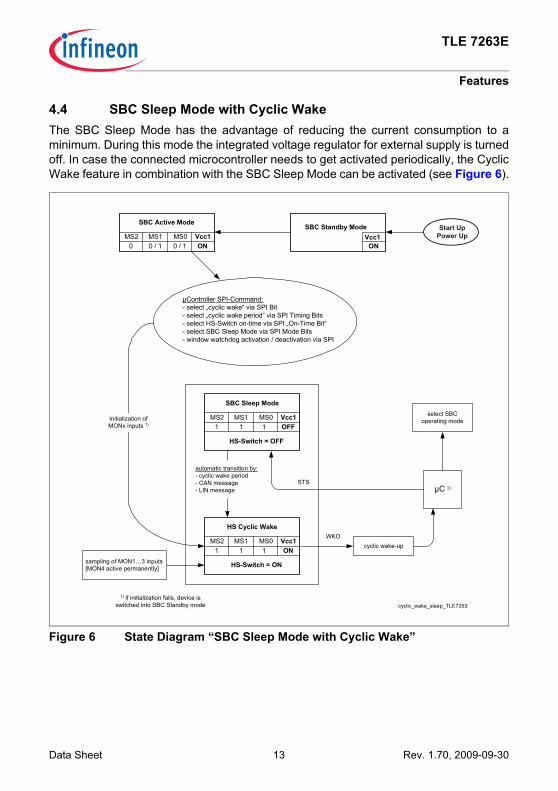
4.4 SBC Sleep Mode with Cyclic WakeThe SBC Sleep Mode has the advantage of reducing the current consumption to aminimum. During this mode the integrated voltage regulator for external supply is turnedoff. In case the connected microcontroller needs to get activated periodically, the CyclicWake feature in combination with the SBC Sleep Mode can be activated (see Figure 6).
Figure 6 State Diagram “SBC Sleep Mode with Cyclic Wake”
Start UpPower Up
cyclic_wake_sleep_TLE7263
SBC Active Mode
MS2ON
Vcc1MS10 0 / 1
MS00 / 1
SBC Sleep Mode
MS2OFFVcc1MS1
1 1MS01
HS-Switch = OFF
HS Cyclic Wake
MS2ON
Vcc1MS11 1
MS01
HS-Switch = ON
µController SPI-Command:- select „cyclic wake“ via SPI Bit- select „cyclic wake period“ via SPI Timing Bits- select HS-Switch on-time via SPI „On-Time Bit“- select SBC Sleep Mode via SPI Mode Bits- window watchdog activation / deactivation via SPI
automatic transition by:- cyclic wake period- CAN message- LIN message
1) if initialization fails, device isswitched into SBC Standby mode
Initialization ofMONx inputs 1)
sampling of MON1…3 inputs[MON4 active permanently]
µC 2)
cyclic wake-upWKO
select SBCoperating mode
STS
SBC Standby Mode
ONVcc1
Data Sheet 13 Rev. 1.70, 2009-09-30
TLE 7263E
Features
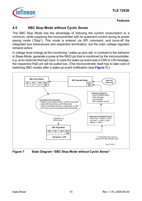
4.5 SBC Stop Mode without Cyclic SenseThe SBC Stop Mode has the advantage of reducing the current consumption to aminimum, while supplying the microcontroller with its quiescent current during its powersaving mode (“Stop”). This mode is entered via SPI command, and turns-off theintegrated bus transceivers and respective termination, but the main voltage regulatorremains active.A voltage level change at the monitoring / wake-up pins will, in contrast to the behaviorin Sleep Mode, generate a pulse at the WKO pin that is monitored by the microcontroller,e.g. at an external interrupt input. In case the wake-up event was a CAN or LIN message,the respective RxD pin will be pulled low. (The microcontroller itself has to take care ofswitching SBC modes after a wake-up event notification (see Figure 7).)
Figure 7 State Diagram “SBC Stop Mode without Cyclic Sense”
Start UpPower Up
stop_TLE7263
SBC Active Mode
MS2ON
Vcc1MS10 0 / 1
MS00 / 1
SBC Stop Mode
MS2ON
Vcc1MS11 1
MS01
HS-Switch = OFF
µController SPI-Command:- disable „cyclic sense function“ via SPI Timing Bits- select SBC Stop Mode via SPI Mode Bits- window watchdog activation / deactivation via SPI [„off“ once current consumption below threshold]
Initialization of MONx inputs 1)
transition caused by:- event at MONx inputs- CAN message- LIN message [SPI indicates source]
1) if initialization fails, device is switched into SBC Standby mode
wake event notification [to µC]:- CAN msg. => RxDCAN (low)- LIN msg. => RxDLIN (low)- MONx => WKO
SBC Standby Mode
ONVcc1
Data Sheet 14 Rev. 1.70, 2009-09-30
TLE 7263E
Features
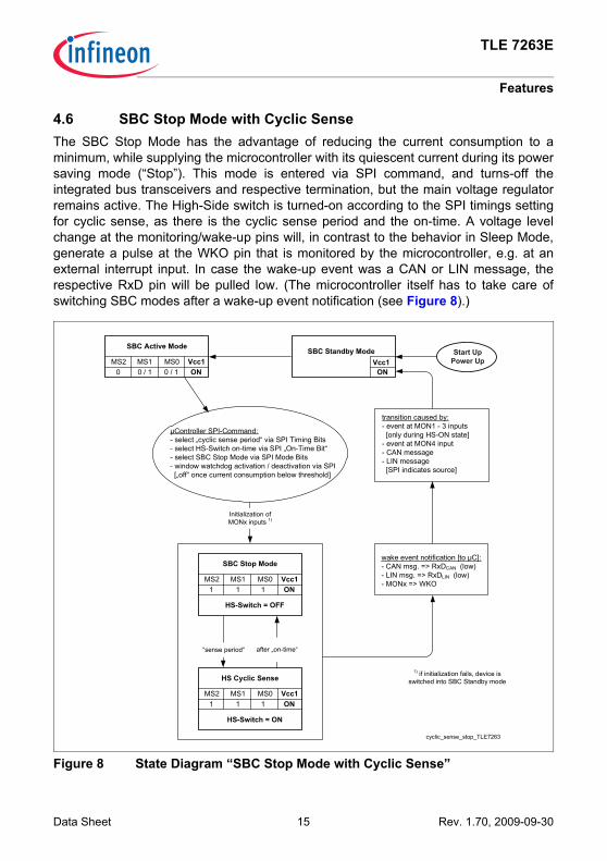
4.6 SBC Stop Mode with Cyclic SenseThe SBC Stop Mode has the advantage of reducing the current consumption to aminimum, while supplying the microcontroller with its quiescent current during its powersaving mode (“Stop”). This mode is entered via SPI command, and turns-off theintegrated bus transceivers and respective termination, but the main voltage regulatorremains active. The High-Side switch is turned-on according to the SPI timings settingfor cyclic sense, as there is the cyclic sense period and the on-time. A voltage levelchange at the monitoring/wake-up pins will, in contrast to the behavior in Sleep Mode,generate a pulse at the WKO pin that is monitored by the microcontroller, e.g. at anexternal interrupt input. In case the wake-up event was a CAN or LIN message, therespective RxD pin will be pulled low. (The microcontroller itself has to take care ofswitching SBC modes after a wake-up event notification (see Figure 8).)
Figure 8 State Diagram “SBC Stop Mode with Cyclic Sense”
Start UpPower Up
cyclic_sense_stop_TLE7263
SBC Active Mode
MS2ON
Vcc1MS10 0 / 1
MS00 / 1
SBC Stop Mode
MS2ON
Vcc1MS11 1
MS01
HS-Switch = OFF
HS Cyclic Sense
MS2ON
Vcc1MS11 1
MS01
HS-Switch = ON
after „on-time“
µController SPI-Command:- select „cyclic sense period“ via SPI Timing Bits- select HS-Switch on-time via SPI „On-Time Bit“- select SBC Stop Mode via SPI Mode Bits- window watchdog activation / deactivation via SPI [„off“ once current consumption below threshold]
“sense period“
Initialization of MONx inputs 1)
transition caused by:- event at MON1 - 3 inputs [only during HS-ON state]- event at MON4 input- CAN message- LIN message [SPI indicates source]
1) if initialization fails, device is switched into SBC Standby mode
wake event notification [to µC]:- CAN msg. => RxDCAN (low)- LIN msg. => RxDLIN (low)- MONx => WKO
SBC Standby Mode
ONVcc1
Data Sheet 15 Rev. 1.70, 2009-09-30
TLE 7263E
Features
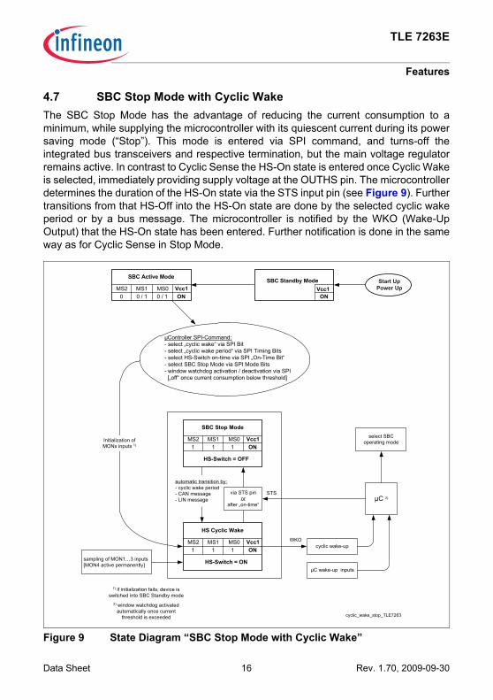
4.7 SBC Stop Mode with Cyclic WakeThe SBC Stop Mode has the advantage of reducing the current consumption to aminimum, while supplying the microcontroller with its quiescent current during its powersaving mode (“Stop”). This mode is entered via SPI command, and turns-off theintegrated bus transceivers and respective termination, but the main voltage regulatorremains active. In contrast to Cyclic Sense the HS-On state is entered once Cyclic Wakeis selected, immediately providing supply voltage at the OUTHS pin. The microcontrollerdetermines the duration of the HS-On state via the STS input pin (see Figure 9). Furthertransitions from that HS-Off into the HS-On state are done by the selected cyclic wakeperiod or by a bus message. The microcontroller is notified by the WKO (Wake-UpOutput) that the HS-On state has been entered. Further notification is done in the sameway as for Cyclic Sense in Stop Mode.
Figure 9 State Diagram “SBC Stop Mode with Cyclic Wake”
µC 2)
Start UpPower Up
cyclic_wake_stop_TLE7263
SBC Active Mode
MS2ON
Vcc1MS10 0 / 1
MS00 / 1
SBC Stop Mode
MS2ON
Vcc1MS11 1
MS01
HS-Switch = OFF
HS Cyclic Wake
MS2ON
Vcc1MS11 1
MS01
HS-Switch = ON
cyclic wake-up
µController SPI-Command:- select „cyclic wake“ via SPI Bit- select „cyclic wake period“ via SPI Timing Bits- select HS-Switch on-time via SPI „On-Time Bit“- select SBC Stop Mode via SPI Mode Bits- window watchdog activation / deactivation via SPI [„off“ once current consumption below threshold]
automatic transition by:- cyclic wake period- CAN message- LIN message
WKO
µC wake-up inputs
1) if initialization fails, device isswitched into SBC Standby mode
Initialization ofMONx inputs 1)
2) window watchdog activatedautomatically once current
threshold is exceeded
select SBCoperating mode
sampling of MON1…3 inputs[MON4 active permanently]
via STS pinor
after „on-time“
STS
SBC Standby Mode
ONVcc1
Data Sheet 16 Rev. 1.70, 2009-09-30
TLE 7263E
Features
Continuous Timer Mode (CTM) for “Cyclic Wake Timer”Upon start of the “cyclic wake timer” in Cyclic Wake Mode the operating mode might bechanged to “SBC Active Mode” by the microcontroller, e.g. in order to transmit data viathe CAN or LIN transceiver. In this case the timer continues running with the selectedperiod started in Cyclic Wake Mode. This behavior guarantees the periodic generationof a wake-up signal at the WKO pin, even in case of a mode switch. However, thisprovides that the time spent in SBC Active Mode is not exceeding the selected period.Should a time-out (end of selected period) occur in SBC Active Mode before the CyclicWake Mode is re-entered, the SBC will generate an interrupt signal at its WKO pin if theCTM feature is enabled via the respective SPI bit (see Figure 11). When the CTM feature is set in the SPI, a wake-up event at the CAN bus in “SBC ActiveCAN Sleep” mode or at the LIN bus in the “SBC Active LIN Sleep” mode results inswitching WKO “low” in addition to switching the RxD to “low”.
4.8 Dual Low Dropout Voltage RegulatorThe dual low dropout voltage regulator integrated in the TLE 7263E is able to driveexternal as well as internal loads, e.g. CAN-circuit supplied via VCC2, even in case of abus short circuit. Its output voltage tolerance is better than ±2%. The maximum outputcurrent for external loads is limited to 150 mA (VCC1), e.g. for microcontroller supply, and150 mA (VCC2) for internal CAN module and, e.g. for external sensor supply. The twovoltage regulator outputs are protected against overload and overtemperature. Thethermal pre-warning flag might be used by the microcontroller to reduce the powerdissipation of the TLE 7263E by switching off functions of minor priority until thetemperature threshold of the thermal shutdown is reached. An external reverse current protection is required at the pin VS to prevent the outputcapacitor from being discharged by negative transients or low input voltage.A capacitor of 10 μF at the supply voltage input VS buffers the input voltage. Incombination with the required reverse polarity diode this prevents the device fromdetecting power down conditions in case of negative transients on the supply line.Stability of the output voltage is guaranteed for output capacitors CQ ≥ 100 nF,nevertheless it is recommended to use capacitors CQ ≥ 10 μF to buffer the output voltageand therefore improve the reset behavior at input voltage transients.
Data Sheet 17 Rev. 1.70, 2009-09-30
TLE 7263E
Features
4.9 CAN TransceiverThe TLE 7263E is optimized for high speed data transmission up to 1 MBaud inautomotive applications and is compatible to the ISO 11898 standard. It works as aninterface between the CAN protocol controller and the physical bus lines.This HS-CAN module also supports extended bus error detection via a general error flagas well as individual notification flags, e.g. temperature shutdown and TxD time-out flag,within the SPI.To reduce EMI the dynamic slopes of the CANL and CANH signals both are limited andsymmetric. This allows the use of an unshielded twisted or parallel pair of wires for thebus.Furthermore there is implemented a time-out feature to prevent the bus from beingblocked by a permanently dominant TxD input signal. Both, the CANL and CANH outputstage are automatically disabled after the delay time tTxD.In order to protect the transceiver output stages from being damaged by shorts on thebus lines, current limiting circuits are integrated. The CANL and CANH output stagerespectively are protected by an additional temperature sensor, that disables them assoon as the junction temperature exceeds the maximum value. During the temperatureshut-down condition of the CAN output stages receiving messages from the bus lines isstill possible.Wake-Up Indication: A bus wake-up via a CAN message (minimum dominant timet > tWU) from low power mode sets the RxD pin and the WKO pin to low. In addition, theVcc2, which supplies the CAN output stage is switched ON.The CAN transceiver has tobe enabled to reset the wake-up capability after a bus wake event and after power-up.Bus Failure Flag: signalizes a bus line short circuit condition to GND, VS or VCCx viaSPI bit 11 in the SPI Output Data “CAN Bus Failure”.Remarks: Flag is set after four consecutive recessive to dominant cycles on pin TxDwhen trying to drive the bus dominant. The bus failure flag is cleared upon 4 recessiveto dominant edges at TxD without failure condition.Local Failure Flag: signalizes the local failure conditions listed in the text below via SPIbit 10 in the SPI Output Data “CAN Local Failure”.Remark: Flag is cleared upon dominant level at RxD while TxD is recessive.General: release of the transmitter stage only after transition into CAN RxD Only modeand transition back into SBC Active Mode.TxD Dominant Failure DetectionAt permanent dominant signal for t > tTxD at TxD the local failure flag is set and thetransmitter stage is turned off.Remarks: none
Data Sheet 18 Rev. 1.70, 2009-09-30
TLE 7263E
Features
RxD Permanent Recessive ClampingInternal RxD signal does not match signal at RxD pin because the RxD pin is pulled toHIGH (permanent HIGH). This results in setting the local failure flag and disabling of thereceiver stageRemark: the flag is cleared when RxD signal gets dominant.TxD to RxD Short CircuitCaused by a short circuit between RxD and TxD. The local failure flag is set and thetransmitter stage is disabled.Remark: the flag is cleared once the short circuit condition is removed.Bus Dominant ClampingAt a permanent dominant signal at the CAN bus for t > tBUS the local failure flag is set.Remark: noneOver Temperature DetectionOnce the maximum junction temperature at the driving stages exceeded, the local failureflag is set and the transmitter stage is disabled.Remark: the flag is cleared once RxD gets dominant. Bus only released after the nextdominant bit in TxD.
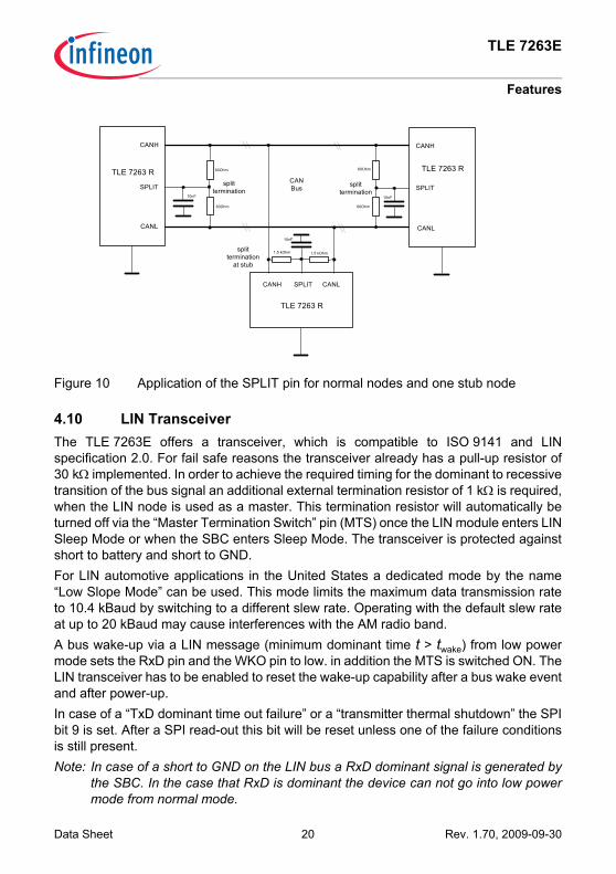
Split CircuitThe split circuitry is activated during SBC Active and RxD Only Mode and deactivated(SPLIT pin high omic) during SBC Sleep, Stop and Standby Mode. The SPLIT pin is usedto stabilize the recessive common mode signal in SBC Active Mode and RxD Only mode.This is realized with a stabilized voltage of 0.5 VCC2 at the SPLIT pin. A correct application of the SPLIT pin is shown in Figure 10. The split termination for theleft and right node is realized with two 60 Ohm resistances and one 10nF capacitor. Thecenter node in this example is a stub node and the recommended value for the splitresistances is 1.5 kOhm.
Data Sheet 19 Rev. 1.70, 2009-09-30
TLE 7263E
Features
Figure 10 Application of the SPLIT pin for normal nodes and one stub node
4.10 LIN TransceiverThe TLE 7263E offers a transceiver, which is compatible to ISO 9141 and LINspecification 2.0. For fail safe reasons the transceiver already has a pull-up resistor of30 kΩ implemented. In order to achieve the required timing for the dominant to recessivetransition of the bus signal an additional external termination resistor of 1 kΩ is required,when the LIN node is used as a master. This termination resistor will automatically beturned off via the “Master Termination Switch” pin (MTS) once the LIN module enters LINSleep Mode or when the SBC enters Sleep Mode. The transceiver is protected againstshort to battery and short to GND.For LIN automotive applications in the United States a dedicated mode by the name“Low Slope Mode” can be used. This mode limits the maximum data transmission rateto 10.4 kBaud by switching to a different slew rate. Operating with the default slew rateat up to 20 kBaud may cause interferences with the AM radio band.A bus wake-up via a LIN message (minimum dominant time t > twake) from low powermode sets the RxD pin and the WKO pin to low. in addition the MTS is switched ON. TheLIN transceiver has to be enabled to reset the wake-up capability after a bus wake eventand after power-up.In case of a “TxD dominant time out failure” or a “transmitter thermal shutdown” the SPIbit 9 is set. After a SPI read-out this bit will be reset unless one of the failure conditionsis still present.Note: In case of a short to GND on the LIN bus a RxD dominant signal is generated by
the SBC. In the case that RxD is dominant the device can not go into low powermode from normal mode.
CANH
CANL
splittermination
splittermination
CANBus
CANH
CANL
SPLITSPLIT
60Ohm
60Ohm
60Ohm
60Ohm
10nF10nF
TLE 7263 R
CANH CANLSPLIT
10nF
splittermination
at stub
1,5 kOhm 1,5 kOhm
TLE 7263 R
TLE 7263 R
Data Sheet 20 Rev. 1.70, 2009-09-30
TLE 7263E
Features
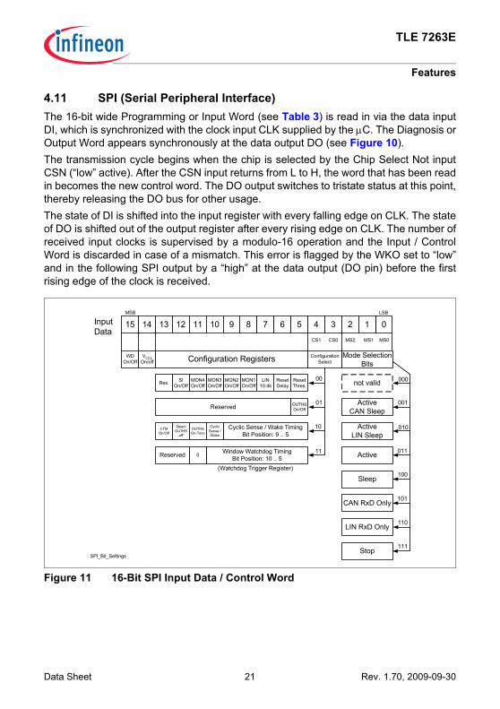
4.11 SPI (Serial Peripheral Interface)The 16-bit wide Programming or Input Word (see Table 3) is read in via the data inputDI, which is synchronized with the clock input CLK supplied by the μC. The Diagnosis orOutput Word appears synchronously at the data output DO (see Figure 10).The transmission cycle begins when the chip is selected by the Chip Select Not inputCSN (“low” active). After the CSN input returns from L to H, the word that has been readin becomes the new control word. The DO output switches to tristate status at this point,thereby releasing the DO bus for other usage.The state of DI is shifted into the input register with every falling edge on CLK. The stateof DO is shifted out of the output register after every rising edge on CLK. The number ofreceived input clocks is supervised by a modulo-16 operation and the Input / ControlWord is discarded in case of a mismatch. This error is flagged by the WKO set to “low”and in the following SPI output by a “high” at the data output (DO pin) before the firstrising edge of the clock is received.
Figure 11 16-Bit SPI Input Data / Control Word
15 14 13 12 11 10 89 7 6 5 4 3 2 01
Mode SelectionBits
ConfigurationSelectConfiguration Registers
OUTHSOn/Off
WDOn/Off
InputData
Active
ActiveLIN Sleep
Sleep
Reserved
000
001
010
011
100
101
00
10
ResetThres.
ResetDelay
Window Watchdog TimingBit Position: 10 .. 5
MON2On/Off
MON3On/Off
MON4On/Off
110
111
11
01
LIN10.4k
MON1On/OffRes.
Reserved
(Watchdog Trigger Register)
SIOn/Off
VCC2On/off
Cyclic Sense / Wake TimingBit Position: 9 .. 5
0
SPI_Bit_Settings
not valid
LIN RxD Only
Stop
LSBMSB
MS0MS1MS2CS0CS1
CTMOn/Off
SelectOUTHS
„off“
OUTHSOn-Time
CyclicSense /Wake
ActiveCAN Sleep
CAN RxD Only
Data Sheet 21 Rev. 1.70, 2009-09-30
TLE 7263E
Features
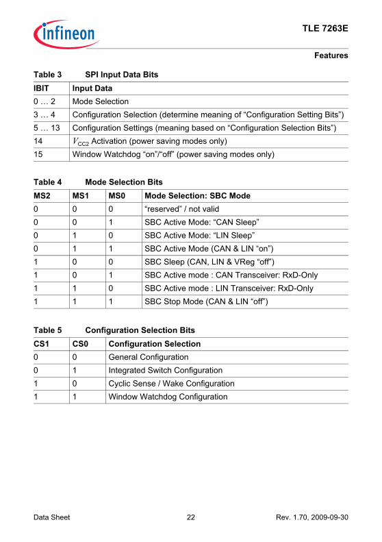
Table 3 SPI Input Data BitsIBIT Input Data0 … 2 Mode Selection3 … 4 Configuration Selection (determine meaning of “Configuration Setting Bits”)5 … 13 Configuration Settings (meaning based on “Configuration Selection Bits”)14 VCC2 Activation (power saving modes only)15 Window Watchdog “on”/“off” (power saving modes only)
Table 4 Mode Selection BitsMS2 MS1 MS0 Mode Selection: SBC Mode0 0 0 “reserved” / not valid0 0 1 SBC Active Mode: “CAN Sleep”0 1 0 SBC Active Mode: “LIN Sleep”0 1 1 SBC Active Mode (CAN & LIN “on”)1 0 0 SBC Sleep (CAN, LIN & VReg “off”)1 0 1 SBC Active mode : CAN Transceiver: RxD-Only1 1 0 SBC Active mode : LIN Transceiver: RxD-Only1 1 1 SBC Stop Mode (CAN & LIN “off”)
Table 5 Configuration Selection BitsCS1 CS0 Configuration Selection0 0 General Configuration0 1 Integrated Switch Configuration1 0 Cyclic Sense / Wake Configuration1 1 Window Watchdog Configuration
Data Sheet 22 Rev. 1.70, 2009-09-30
TLE 7263E
Features
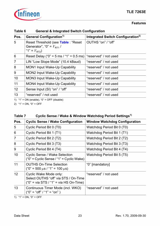
Table 6 General & Integrated Switch ConfigurationPos. General Configuration1) Integrated Switch Configuration2)
5 Reset Threshold (see Table : “Reset Generator”, “0” = VRT1 /“1” = VRT2)
OUTHS “on” / “off”
6 Reset Delay (“0” = 5 ms / “1” = 0.5 ms) “reserved” / not used7 LIN “Low Slope Mode” (10.4 kBaud) “reserved” / not used8 MON1 Input Wake-Up Capability “reserved” / not used9 MON2 Input Wake-Up Capability “reserved” / not used10 MON3 Input Wake-Up Capability “reserved” / not used11 MON4 Input Wake-Up Capability “reserved” / not used12 Sense Input (SI) “on” / “off” “reserved” / not used13 “reserved” / not used “reserved” / not used1) “1” = ON (enable), “0” = OFF (disable)2) “1” = ON, “0” = OFF
Table 7 Cyclic Sense / Wake & Window Watchdog Period Settings1)
1) “1” = ON, “0” = OFF
Pos. Cyclic Sense / Wake Configuration Window Watchdog Configuration5 Cyclic Period Bit 0 (T0) Watchdog Period Bit 0 (T0)6 Cyclic Period Bit 1 (T1) Watchdog Period Bit 1 (T1)7 Cyclic Period Bit 2 (T2) Watchdog Period Bit 2 (T2)8 Cyclic Period Bit 3 (T3) Watchdog Period Bit 3 (T3)9 Cyclic Period Bit 4 (T4) Watchdog Period Bit 4 (T4)10 Cyclic Sense / Wake Selection
(“0” = Cyclic Sense / “1” = Cyclic Wake)Watchdog Period Bit 5 (T5)
11 OUTHS On-Time Selection(“0” = 500 μs / “1” = 100 μs)
“0” [mandatory]
12 Cyclic Wake Mode only:Select OUTHS “off” via STS / On-Time(“0” = via STS / “1” = via HS On-Time)
“reserved” / not used
13 Continuous Timer Mode (incl. WKO)(“0” = “off” / “1” = “on” )
“reserved” / not used
Data Sheet 23 Rev. 1.70, 2009-09-30
TLE 7263E
Features
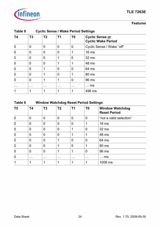
Table 8 Cyclic Sense / Wake Period SettingsT4 T3 T2 T1 T0 Cyclic Sense or
Cyclic Wake Period0 0 0 0 0 Cyclic Sense / Wake “off”0 0 0 0 1 16 ms0 0 0 1 0 32 ms0 0 0 1 1 48 ms0 0 1 0 0 64 ms0 0 1 0 1 80 ms0 0 1 1 0 96 ms… … … … … … ms1 1 1 1 1 496 ms
Table 9 Window Watchdog Reset Period SettingsT5 T4 T3 T2 T1 T0 Window Watchdog
Reset Period0 0 0 0 0 0 “not a valid selection”0 0 0 0 0 1 16 ms0 0 0 0 1 0 32 ms0 0 0 0 1 1 48 ms0 0 0 1 0 0 64 ms0 0 0 1 0 1 80 ms0 0 0 1 1 0 96 ms0 … … … … … … ms1 1 1 1 1 1 1008 ms
Data Sheet 24 Rev. 1.70, 2009-09-30
TLE 7263E
Features
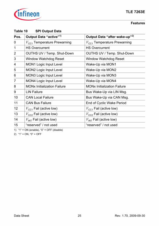
Table 10 SPI Output DataPos. Output Data “active”1) Output Data “after wake-up”2)
0 VCC1 Temperature Prewarning VCC1 Temperature Prewarning1 HS Overcurrent HS Overcurrent2 OUTHS UV / Temp. Shut-Down OUTHS UV / Temp. Shut-Down3 Window Watchdog Reset Window Watchdog Reset4 MON1 Logic Input Level Wake-Up via MON15 MON2 Logic Input Level Wake-Up via MON26 MON3 Logic Input Level Wake-Up via MON37 MON4 Logic Input Level Wake-Up via MON48 MONx Initialization Failure MONx Initialization Failure9 LIN Failure Bus Wake-Up via LIN Msg.10 CAN Local Failure Bus Wake-Up via CAN Msg.11 CAN Bus Failure End of Cyclic Wake Period12 VCC1 Fail (active low) VCC1 Fail (active low)13 VCC2 Fail (active low) VCC2 Fail (active low)14 VINT Fail (active low) VINT Fail (active low)15 “reserved” / not used “reserved” / not used1) “1” = ON (enable), “0” = OFF (disable)2) “1” = ON, “0” = OFF
Data Sheet 25 Rev. 1.70, 2009-09-30
TLE 7263E
Features
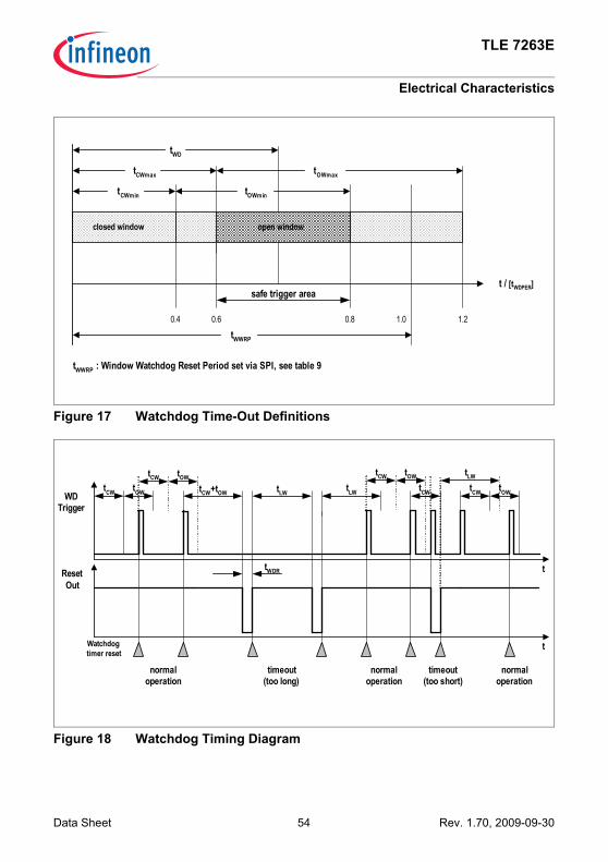
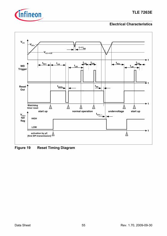
4.12 Window Watchdog, ResetWhen the output voltage Vcc1 exceeds the reset threshold voltage the reset output RO isswitched HIGH after a delay time of typ. 5 ms. This is necessary for a defined start of themicrocontroller when the application is switched on. As soon as an undervoltagecondition of the output voltage (VCC1 < VRT) appears, the reset output RO is switchedLOW again. The LOW signal is guaranteed down to an output voltage VCC1 ≥ 1 V. Pleaserefer to Figure 19, Reset Timing Diagram.After the above described delayed reset (LOW to HIGH transition of RO) the windowwatchdog circuit is started by opening a long open window of typ. 64 ms. The long openwindow allows the microcontroller to run its initialization sequences and then to triggerthe watchdog via the SPI. A watchdog trigger is detected as a write access to the“window watchdog period bit field” within the SPI control word. In order to distinguish thewatchdog from the cyclic sense/wake timing register the “Configuration Select Bits”needs to be set accordingly (see “SPI (Serial Peripheral Interface)” on Page 21). Thetrigger is accepted when the CSN input becomes HIGH after the transmission of the SPIword.A correct watchdog trigger results in starting the window watchdog by opening a closedwindow with a width of 50% of the selected window watchdog reset period. This period,selected via the window watchdog timing bit field, is in the range between 16 ms and1008 ms. This closed window is followed by a open window, with a width of 50% of theselected period. From now on the microcontroller has to service the watchdog byperiodically writing to the window watchdog timing bit field. This write access has to meetthe open window. A correct watchdog service immediately results in starting the nextclosed window (see Figure 17 "Watchdog Time-Out Definitions" on Page 54, safetrigger area).Should the trigger signal not meet the open window a watchdog reset is created bysetting the reset output RO low (see Reset delay time tRD). Then the watchdog againstarts by opening a long open window. In addition, a “window watchdog reset flag” is setwithin the SPI until the next successful watchdog trigger to monitor a watchdog reset. Forfail safe reasons the TLE 7263E is automatically switched in SBC Standby mode if awatchdog trigger failure occurs. This minimizes the power consumption in case of apermanent faulty microcontroller.In case of a watchdog reset the watchdog immediately starts with a long open windowin SBC Standby Mode.When entering a low power mode the watchdog can be requested to be disabled via anSPI bit (see “SPI (Serial Peripheral Interface)” on Page 21). Upon this request thewatchdog is only turned off once the current consumption at VCC1 falls below the“watchdog current threshold”.
Data Sheet 26 Rev. 1.70, 2009-09-30
TLE 7263E
Features
4.13 Sense Comparator using Sense Input SI and Interrupt Output INT
The sense comparator (early warning function) compares a voltage defined by the userto an internal reference voltage. Therefore the voltage to be supervised has to be scaleddown by a voltage divider in order to compare it to the internal sense threshold VSIth. Thisfeature can be used e.g. to supervise the battery voltage in front of the reverse protectiondiode. The microcontroller is given a prewarning before an undervoltage reset due to lowinput voltage occurs. The prewarning is flagged by setting the interrupt output INT low inSBC Active, Standby, and Stop, as well as in CAN Receive - Only Mode, when activatedby SPI. In SBC Sleep Mode the sense function is inactive.Calculation of the voltage divider can be easily done since the sense input current canbe neglected. An internal blanking time prevents from false triggering due to linetransients. Further improvement is possible by the use of an external ceramic capacitorat the SI pin (see Figure 22, Application Circuit).
4.14 VINT/VCC Fail Detection via SPI BitShould the internal supply voltage become lower than the internal threshold VINT, th (typ.2.5 V) the VINT-Fail, threshold SPI bit will be reset in order to indicate the low voltagecondition. All other SPI settings are also reset by this condition. The VINT Fail feature canalso be used to give an indication when the ECU has been changed and therefore a pre-setting routine of the microcontroller has to be started.Further there is also a VCC monitor implemented, where the VCCx is compared to thethreshold voltage VCCx-Fail, threshold and the VCC SPI bit is reset accordingly. Thismonitoring is only available during voltage-regulator operation.
4.15 Monitoring / Wake-Up Inputs MON1/2/3/4 and Wake-Up Output WKO
In addition to a wake-up from SBC Sleep mode via the CAN or LIN bus lines it is alsopossible to wake-up the TLE 7263E from low power mode via the monitoring/wake-upinputs. These inputs are sensitive to a transition of the voltage level, either from high tolow or vice versa. Monitoring is available in Active Mode and indicates the voltage levelof the inputs.A positive or negative voltage edge at MONx in SBC Sleep or Stop Mode results insetting the output WKO low to signal a wake-up. After a wake-up via MONx the firsttransmission of the SPI diagnosis word in SBC Standby mode indicates the wake-upsource. Further SPI status word transmissions show the logic level of the monitoringinputs.When switching the TLE 7263E into SBC Sleep mode (cyclic sense feature activated)the voltage level at the wake-up inputs is sensed 2 times to initialize the referencevoltage. Should this initialization fail (2 samples are unequal) the device is automatically
Data Sheet 27 Rev. 1.70, 2009-09-30
TLE 7263E
Features
set in SBC Standby mode and the initialization error is shown indicated in the SPI statusword.To have a defined level at a floating MONx pin a hold current is implemented. For high level at MONx a pull up current IPU,MON is driven out of the MONx pin, for low level at MONx a pull down current IPD,MON is drawn into the MONx pin.
4.16 High Side SwitchThe high side output OUTHS is able to switch loads up to 150 mA. Its on-resistance is2.5 Ω typ. @ 25 °C. In SBC Active, Standby, as well as in CAN and LIN Receive-Onlymode the high side output is switched on and off, respectively via an SPI input bit.To supply external wake-up circuits in SBC Sleep Mode the output OUTHS can beperiodically switched on by the TLE 7263E itself. How Cyclic Sense works and how it isactivated is described in detail in “Operation Modes” on Page 9. Beside the cyclicsense period can the on-time of the OUTHS be programmed to either 500 μs (defaultsetting) or 100 μs via SPI input bit. OUTHS undervoltage, temperature shutdown,overcurrent as well as a temperature pre-warning is indicated by the SPI status word.The OUTHS is protected against short circuit and overload. As soon as the undervoltagecondition of the supply voltage is met (VS < VUVOFF), the switch is automatically disabledby the undervoltage lockout circuit. Moreover the switch is automatically disabled whena reset or watchdog reset occurs.
4.17 Fail Safe FeatureThe output FSO becomes HIGH when the watchdog is correctly serviced by themicrocontroller for the fourth time. As soon as either an undervoltage reset or watchdogreset occurs, it is set LOW again. This feature is very useful to control critical applicationsindependent of the microcontroller e.g. to disable the power supply in case of amicrocontroller failure.
4.18 Send to Sleep Input STSDuring Cyclic Wake the STS input is used to switch the SBC back to a low current mode(High-Side switch “off”) when the microcontroller has completed its tasks during theperiodic wake-up phase, and before it enters its power saving mode (“Stop”) again.
4.19 Flash Program ModeFor flash programming it is useful to disable the window watchdog function. This can bedone by applying a voltage of VINT > 7.0 V at pin INT. This is useful e.g. if the flash-memory of the micro has to be programmed and therefore a regular watchdog triggeringis not possible.
Data Sheet 28 Rev. 1.70, 2009-09-30
TLE 7263E
Features
Additionally, the transmission rate of the integrated LIN transceiver will be changed tomaximal 150 kBaud.The Sense Comparator using Sense Input and Interrupt Output INT can not be used withFlash Program Mode. The Sense Input feature must be switched off via SPI.
Hints for Unused Pins• SI: connect to GND• OUTHS: leave open• MON1/2/3/4: connect to GND• INT / WKO: leave open• RO / FSO: leave open
Data Sheet 29 Rev. 1.70, 2009-09-30
TLE 7263E
General Product Characteristics
5 General Product Characteristics
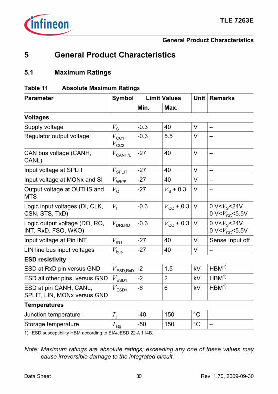
5.1 Maximum Ratings
Note: Maximum ratings are absolute ratings; exceeding any one of these values maycause irreversible damage to the integrated circuit.
Table 11 Absolute Maximum RatingsParameter Symbol Limit Values Unit Remarks
Min. Max.VoltagesSupply voltage VS -0.3 40 V –Regulator output voltage VCC1,
VCC2
-0.3 5.5 V –
CAN bus voltage (CANH, CANL)
VCANH/L -27 40 V –
Input voltage at SPLIT VSPLIT -27 40 V –Input voltage at MONx and SI VWK/SI -27 40 V –Output voltage at OUTHS and MTS
VO -27 VS + 0.3 V –
Logic input voltages (DI, CLK, CSN, STS, TxD)
VI -0.3 VCC + 0.3 V 0 V<VS<24V0 V<VCC<5.5V
Logic output voltage (DO, RO, INT, RxD, FSO, WKO)
VDRI,RD -0.3 VCC + 0.3 V 0 V<VS<24V0 V<VCC<5.5V
Input voltage at Pin INT VINT -27 40 V Sense Input offLIN line bus input voltages Vbus -27 40 V –ESD resistivityESD at RxD pin versus GND VESD,RxD -2 1.5 kV HBM1)
1) ESD susceptibility HBM according to EIA/JESD 22-A 114B.
ESD all other pins. versus GND VESD1 -2 2 kV HBM1)
ESD at pin CANH, CANL, SPLIT, LIN, MONx versus GND
VESD1 -6 6 kV HBM1)
TemperaturesJunction temperature Tj -40 150 °C –Storage temperature Tstg -50 150 °C –
Data Sheet 30 Rev. 1.70, 2009-09-30
TLE 7263E
General Product Characteristics
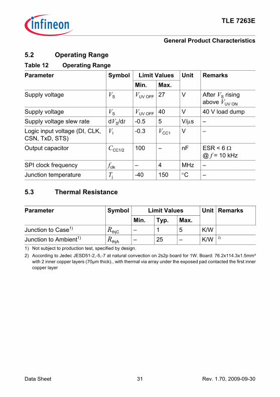
5.2 Operating Range
5.3 Thermal Resistance
Table 12 Operating RangeParameter Symbol Limit Values Unit Remarks
Min. Max.Supply voltage VS VUV OFF 27 V After VS rising
above VUV ON
Supply voltage VS VUV OFF 40 V 40 V load dumpSupply voltage slew rate dVS/dt -0.5 5 V/μs –Logic input voltage (DI, CLK, CSN, TxD, STS)
VI -0.3 VCC1 V –
Output capacitor CCC1/2 100 – nF ESR < 6 Ω@ f = 10 kHz
SPI clock frequency fclk – 4 MHz –Junction temperature Tj -40 150 °C –
Parameter Symbol Limit Values Unit RemarksMin. Typ. Max.
Junction to Case1)
1) Not subject to production test, specified by design.
RthjC – 1 5 K/WJunction to Ambient1) RthjA – 25 – K/W 2)
2) According to Jedec JESD51-2,-5,-7 at natural convection on 2s2p board for 1W. Board: 76.2x114.3x1.5mm³with 2 inner copper layers (70µm thick)., with thermal via array under the exposed pad contacted the first innercopper layer
Data Sheet 31 Rev. 1.70, 2009-09-30
TLE 7263E
Electrical Characteristics
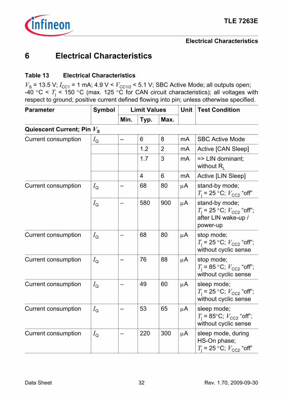
6 Electrical Characteristics
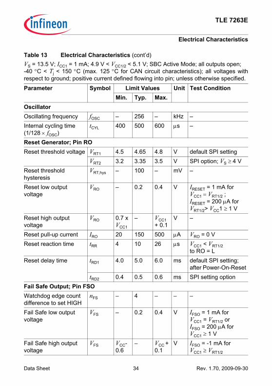
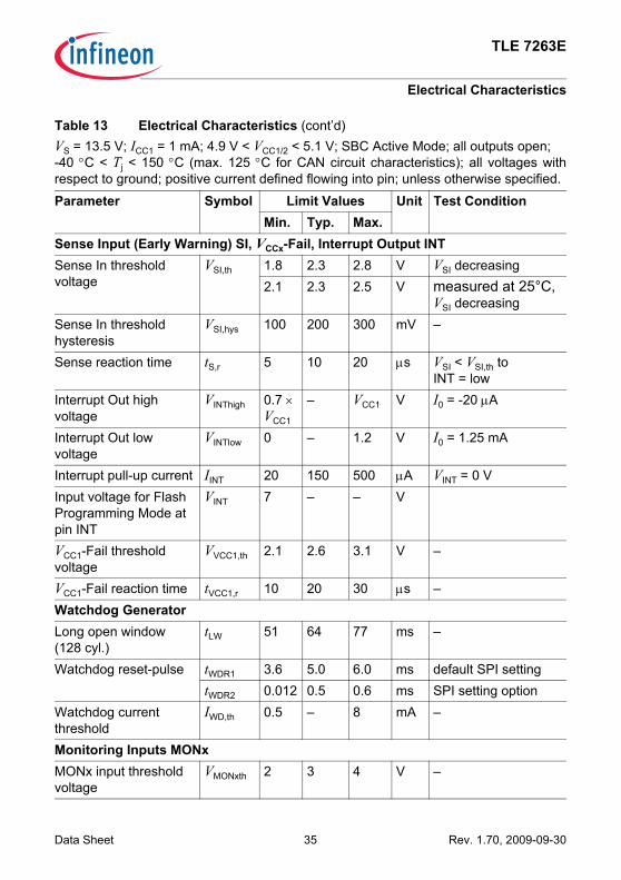
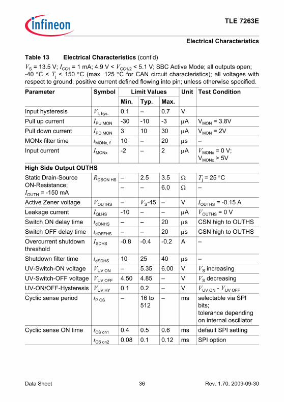
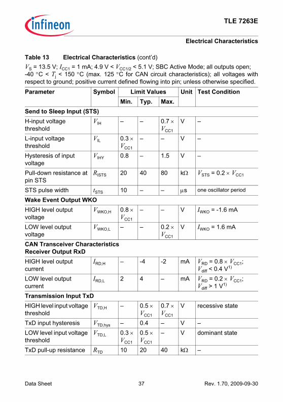
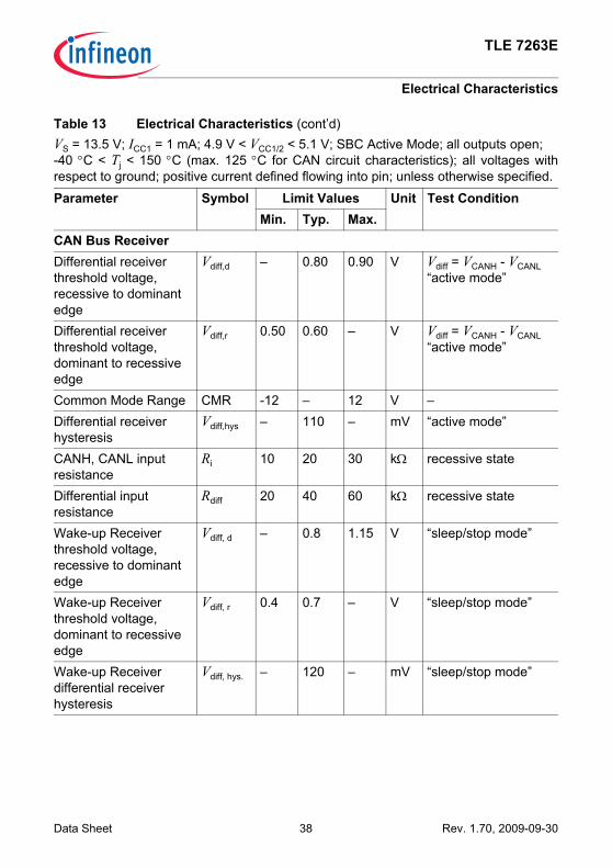
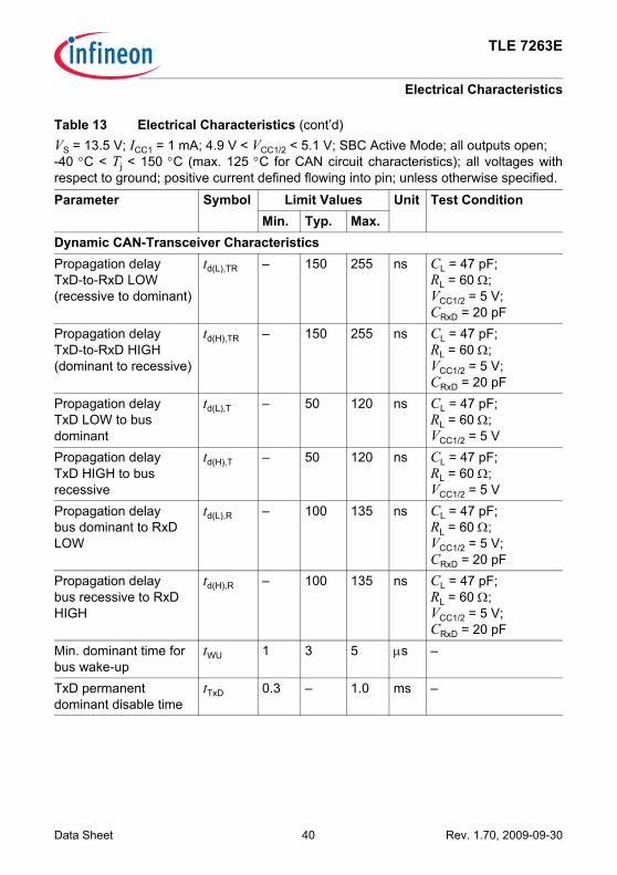
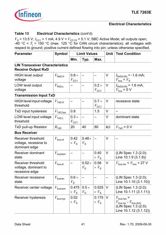
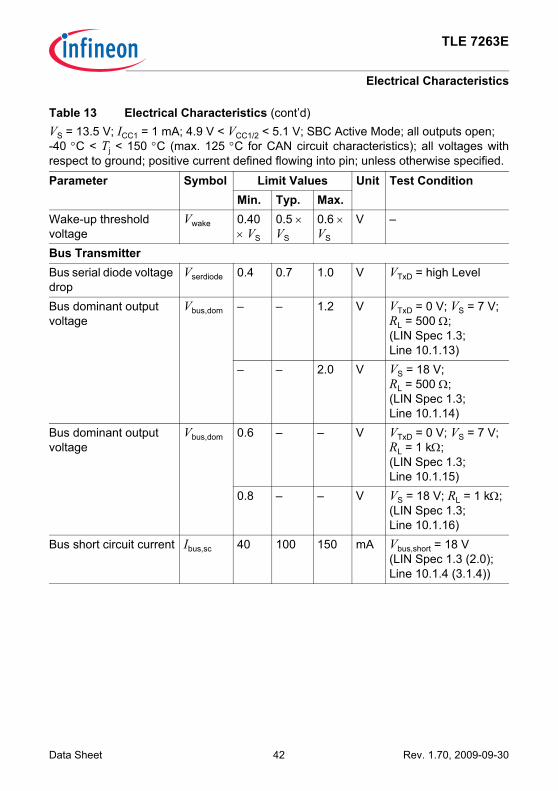
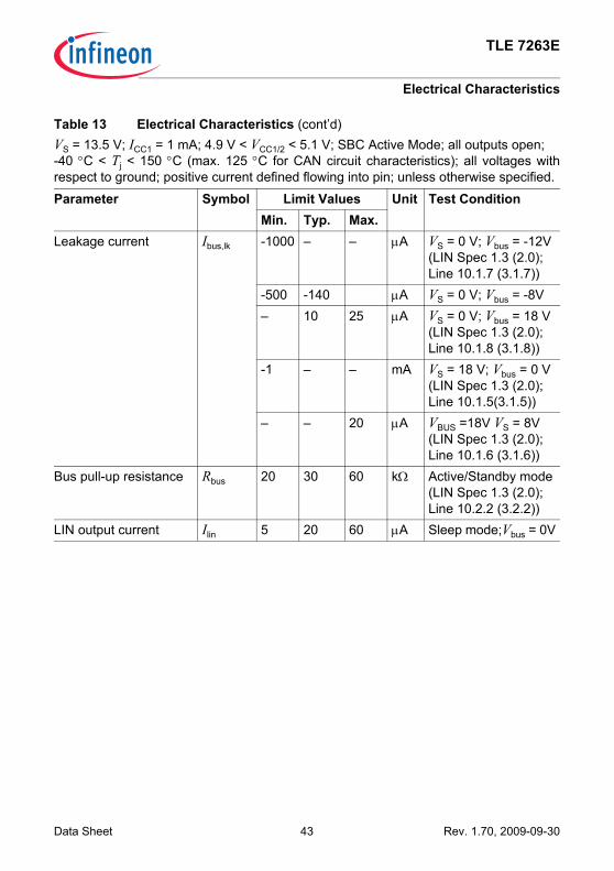
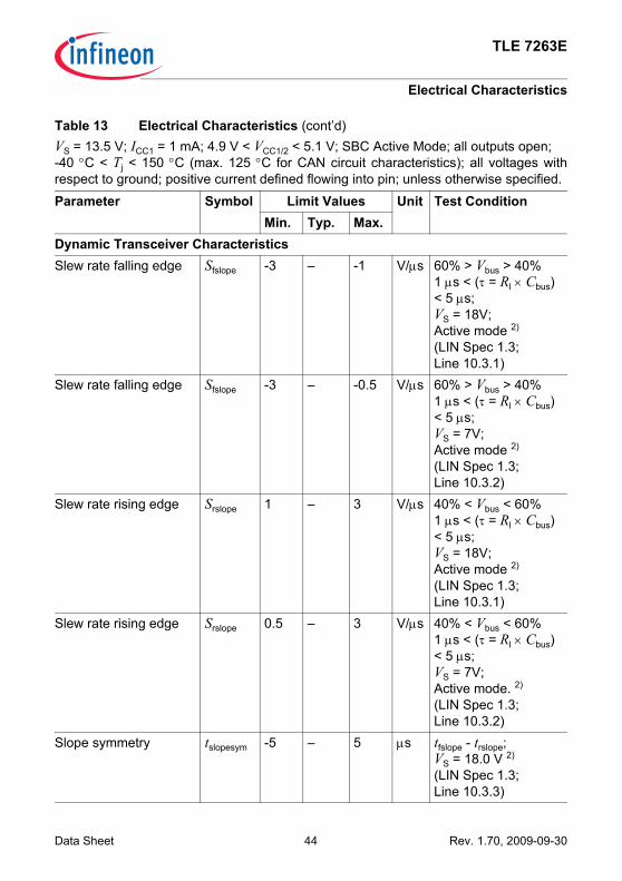
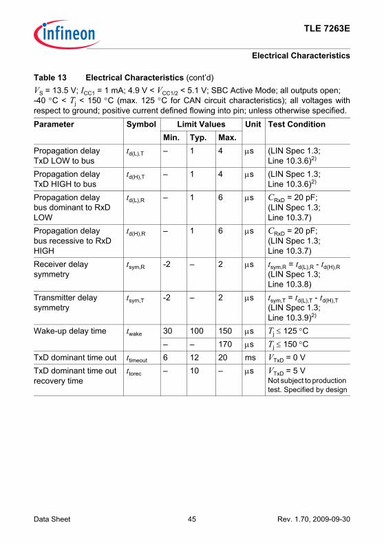
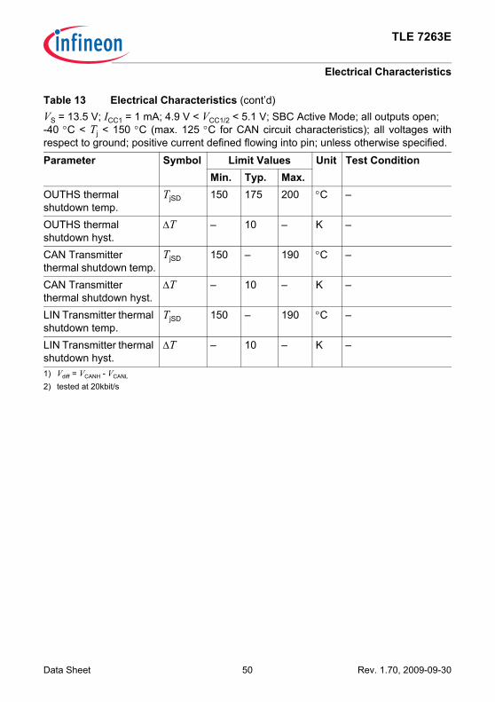
Table 13 Electrical CharacteristicsVS = 13.5 V; ICC1 = 1 mA; 4.9 V < VCC1/2 < 5.1 V; SBC Active Mode; all outputs open;-40 °C < Tj < 150 °C (max. 125 °C for CAN circuit characteristics); all voltages withrespect to ground; positive current defined flowing into pin; unless otherwise specified.
Parameter Symbol Limit Values Unit Test ConditionMin. Typ. Max.
Quiescent Current; Pin VS
Current consumption IQ – 6 8 mA SBC Active Mode1.2 2 mA Active [CAN Sleep]1.7 3 mA => LIN dominant;
without RL
4 6 mA Active [LIN Sleep]Current consumption IQ – 68 80 μA stand-by mode;
Tj = 25 °C; VCC2 “off”IQ – 580 900 μA stand-by mode;
Tj = 25 °C; VCC2 “off”; after LIN wake-up / power-up
Current consumption IQ – 68 80 μA stop mode;Tj = 25 °C; VCC2 “off”; without cyclic sense
Current consumption IQ – 76 88 μA stop mode;Tj = 85 °C; VCC2 “off”; without cyclic sense
Current consumption IQ – 49 60 μA sleep mode;Tj = 25 °C; VCC2 “off”; without cyclic sense
Current consumption IQ – 53 65 μA sleep mode;Tj = 85°C; VCC2 “off”; without cyclic sense
Current consumption IQ – 220 300 μA sleep mode, during HS-On phase;Tj = 25 °C; VCC2 “off”
Data Sheet 32 Rev. 1.70, 2009-09-30
TLE 7263E
Electrical Characteristics
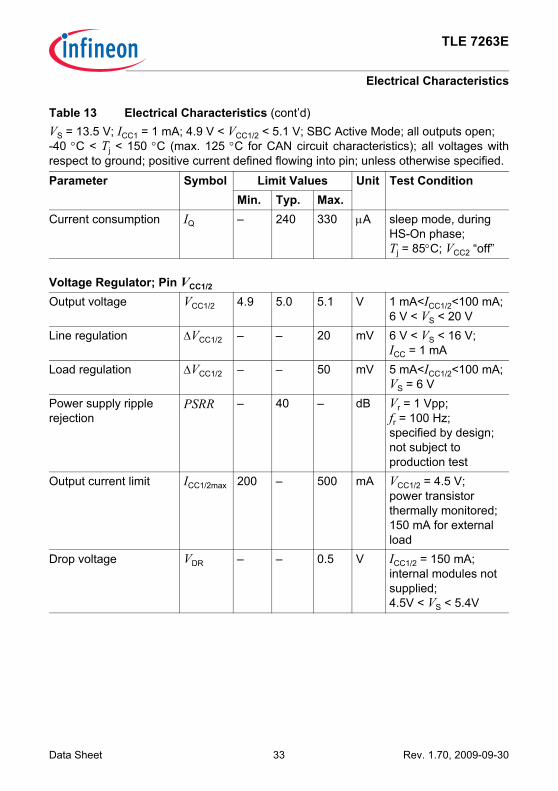
Current consumption IQ – 240 330 μA sleep mode, during HS-On phase;Tj = 85°C; VCC2 “off”
Voltage Regulator; Pin VCC1/2
Output voltage VCC1/2 4.9 5.0 5.1 V 1 mA<ICC1/2<100 mA;6 V < VS < 20 V
Line regulation ΔVCC1/2 – – 20 mV 6 V < VS < 16 V;ICC = 1 mA
Load regulation ΔVCC1/2 – – 50 mV 5 mA<ICC1/2<100 mA;VS = 6 V
Power supply ripple rejection
PSRR – 40 – dB Vr = 1 Vpp;fr = 100 Hz;specified by design; not subject to production test
Output current limit ICC1/2max 200 – 500 mA VCC1/2 = 4.5 V;power transistor thermally monitored;150 mA for external load
Drop voltage VDR – – 0.5 V ICC1/2 = 150 mA; internal modules not supplied; 4.5V < VS < 5.4V
Table 13 Electrical Characteristics (cont’d)VS = 13.5 V; ICC1 = 1 mA; 4.9 V < VCC1/2 < 5.1 V; SBC Active Mode; all outputs open;-40 °C < Tj < 150 °C (max. 125 °C for CAN circuit characteristics); all voltages withrespect to ground; positive current defined flowing into pin; unless otherwise specified.
Parameter Symbol Limit Values Unit Test ConditionMin. Typ. Max.
Data Sheet 33 Rev. 1.70, 2009-09-30
TLE 7263E
Electrical Characteristics
OscillatorOscillating frequency fOSC – 256 – kHz –Internal cycling time(1/128 × fOSC)
tCYL 400 500 600 μs –
Reset Generator; Pin ROReset threshold voltage VRT1 4.5 4.65 4.8 V default SPI setting
VRT2 3.2 3.35 3.5 V SPI option; VS ≥ 4 VReset threshold hysteresis
VRT,hys – 100 – mV –
Reset low output voltage
VRO – 0.2 0.4 V IRESET = 1 mA forVCC1 = VRT1/2 ;IRESET = 200 μA forVRT1/2> VCC1 ≥ 1 V
Reset high output voltage
VRO 0.7 x VCC1
– VCC1 + 0.1
V –
Reset pull-up current IRO 20 150 500 μA VRO = 0 VReset reaction time tRR 4 10 26 μs VCC1 < VRT1/2
to RO = LReset delay time tRD1 4.0 5.0 6.0 ms default SPI setting;
after Power-On-ResettRD2 0.4 0.5 0.6 ms SPI setting option
Fail Safe Output; Pin FSOWatchdog edge count difference to set HIGH
nFS – 4 – – –
Fail Safe low output voltage
VFS – 0.2 0.4 V IFSO = 1 mA forVCC1 = VRT1/2 orIFSO = 200 μA forVCC1 ≥ 1 V
Fail Safe high output voltage
VFS VCC- 0.6
– VCC + 0.1
V IFSO = -1 mA forVCC1 ≥ VRT1/2
Table 13 Electrical Characteristics (cont’d)VS = 13.5 V; ICC1 = 1 mA; 4.9 V < VCC1/2 < 5.1 V; SBC Active Mode; all outputs open;-40 °C < Tj < 150 °C (max. 125 °C for CAN circuit characteristics); all voltages withrespect to ground; positive current defined flowing into pin; unless otherwise specified.
Parameter Symbol Limit Values Unit Test ConditionMin. Typ. Max.
Data Sheet 34 Rev. 1.70, 2009-09-30
TLE 7263E
Electrical Characteristics
Sense Input (Early Warning) SI, VCCx-Fail, Interrupt Output INTSense In threshold voltage
VSI,th 1.8 2.3 2.8 V VSI decreasing2.1 2.3 2.5 V measured at 25°C,
VSI decreasingSense In threshold hysteresis
VSI,hys 100 200 300 mV –
Sense reaction time tS,r 5 10 20 μs VSI < VSI,th toINT = low
Interrupt Out high voltage
VINThigh 0.7 × VCC1
– VCC1 V I0 = -20 μA
Interrupt Out low voltage
VINTlow 0 – 1.2 V I0 = 1.25 mA
Interrupt pull-up current IINT 20 150 500 μA VINT = 0 VInput voltage for Flash Programming Mode at pin INT
VINT 7 – – V
VCC1-Fail threshold voltage
VVCC1,th 2.1 2.6 3.1 V –
VCC1-Fail reaction time tVCC1,r 10 20 30 μs –Watchdog GeneratorLong open window(128 cyl.)
tLW 51 64 77 ms –
Watchdog reset-pulse tWDR1 3.6 5.0 6.0 ms default SPI settingtWDR2 0.012 0.5 0.6 ms SPI setting option
Watchdog current threshold
IWD,th 0.5 – 8 mA –
Monitoring Inputs MONxMONx input threshold voltage
VMONxth 2 3 4 V –
Table 13 Electrical Characteristics (cont’d)VS = 13.5 V; ICC1 = 1 mA; 4.9 V < VCC1/2 < 5.1 V; SBC Active Mode; all outputs open;-40 °C < Tj < 150 °C (max. 125 °C for CAN circuit characteristics); all voltages withrespect to ground; positive current defined flowing into pin; unless otherwise specified.
Parameter Symbol Limit Values Unit Test ConditionMin. Typ. Max.
Data Sheet 35 Rev. 1.70, 2009-09-30
TLE 7263E
Electrical Characteristics
Input hysteresis VI, hys. 0.1 – 0.7 VPull up current IPU,MON -30 -10 -3 μA VMON = 3.8VPull down current IPD,MON 3 10 30 μA VMON = 2VMONx filter time tMONx, f 10 – 20 μs –Input current IMONx -2 – 2 μA VMONx = 0 V;
VMONx > 5VHigh Side Output OUTHSStatic Drain-SourceON-Resistance;IOUTH = -150 mA
RDSON HS – 2.5 3.5 Ω Tj = 25 °C– – 6.0 Ω –
Active Zener voltage VOUTHS – VS-45 – V IOUTHS = -0.15 ALeakage current IQLHS -10 – – μA VOUTHS = 0 VSwitch ON delay time tdONHS – – 20 μs CSN high to OUTHSSwitch OFF delay time tdOFFHS – – 20 μs CSN high to OUTHSOvercurrent shutdown threshold
ISDHS -0.8 -0.4 -0.2 A –
Shutdown filter time tdSDHS 10 25 40 μs –UV-Switch-ON voltage VUV ON – 5.35 6.00 V VS increasingUV-Switch-OFF voltage VUV OFF 4.50 4.85 – V VS decreasingUV-ON/OFF-Hysteresis VUV HY 0.1 0.2 – V VUV ON - VUV OFF
Cyclic sense period tP CS – 16 to 512
– ms selectable via SPI bits;tolerance depending on internal oscillator
Cyclic sense ON time tCS on1 0.4 0.5 0.6 ms default SPI settingtCS on2 0.08 0.1 0.12 ms SPI option
Table 13 Electrical Characteristics (cont’d)VS = 13.5 V; ICC1 = 1 mA; 4.9 V < VCC1/2 < 5.1 V; SBC Active Mode; all outputs open;-40 °C < Tj < 150 °C (max. 125 °C for CAN circuit characteristics); all voltages withrespect to ground; positive current defined flowing into pin; unless otherwise specified.
Parameter Symbol Limit Values Unit Test ConditionMin. Typ. Max.
Data Sheet 36 Rev. 1.70, 2009-09-30
TLE 7263E
Electrical Characteristics
Send to Sleep Input (STS)H-input voltage threshold
VIH – – 0.7 × VCC1
V –
L-input voltage threshold
VIL 0.3 × VCC1
– – V –
Hysteresis of input voltage
VIHY 0.8 – 1.5 V –
Pull-down resistance at pin STS
RISTS 20 40 80 kΩ VSTS = 0.2 × VCC1
STS pulse width tSTS 10 – – μs one oscillator period
Wake Event Output WKOHIGH level output voltage
VWKO,H 0.8 × VCC1
– – V IWKO = -1.6 mA
LOW level output voltage
VWKO,L – – 0.2 × VCC1
V IWKO = 1.6 mA
CAN Transceiver CharacteristicsReceiver Output RxDHIGH level output current
IRD,H – -4 -2 mA VRD = 0.8 × VCC1;Vdiff < 0.4 V1)
LOW level output current
IRD,L 2 4 – mA VRD = 0.2 × VCC1;Vdiff > 1 V1)
Transmission Input TxDHIGH level input voltage threshold
VTD,H – 0.5 × VCC1
0.7 × VCC1
V recessive state
TxD input hysteresis VTD,hys – 0.4 – V –LOW level input voltage threshold
VTD,L 0.3 × VCC1
0.5 × VCC1
– V dominant state
TxD pull-up resistance RTD 10 20 40 kΩ –
Table 13 Electrical Characteristics (cont’d)VS = 13.5 V; ICC1 = 1 mA; 4.9 V < VCC1/2 < 5.1 V; SBC Active Mode; all outputs open;-40 °C < Tj < 150 °C (max. 125 °C for CAN circuit characteristics); all voltages withrespect to ground; positive current defined flowing into pin; unless otherwise specified.
Parameter Symbol Limit Values Unit Test ConditionMin. Typ. Max.
Data Sheet 37 Rev. 1.70, 2009-09-30
TLE 7263E
Electrical Characteristics
CAN Bus ReceiverDifferential receiver threshold voltage,recessive to dominant edge
Vdiff,d – 0.80 0.90 V Vdiff = VCANH - VCANL“active mode”
Differential receiver threshold voltage,dominant to recessive edge
Vdiff,r 0.50 0.60 – V Vdiff = VCANH - VCANL“active mode”
Common Mode Range CMR -12 – 12 V –Differential receiver hysteresis
Vdiff,hys – 110 – mV “active mode”
CANH, CANL input resistance
Ri 10 20 30 kΩ recessive state
Differential input resistance
Rdiff 20 40 60 kΩ recessive state
Wake-up Receiverthreshold voltage,recessive to dominant edge
Vdiff, d – 0.8 1.15 V “sleep/stop mode”
Wake-up Receiverthreshold voltage,dominant to recessive edge
Vdiff, r 0.4 0.7 – V “sleep/stop mode”
Wake-up Receiverdifferential receiver hysteresis
Vdiff, hys. – 120 – mV “sleep/stop mode”
Table 13 Electrical Characteristics (cont’d)VS = 13.5 V; ICC1 = 1 mA; 4.9 V < VCC1/2 < 5.1 V; SBC Active Mode; all outputs open;-40 °C < Tj < 150 °C (max. 125 °C for CAN circuit characteristics); all voltages withrespect to ground; positive current defined flowing into pin; unless otherwise specified.
Parameter Symbol Limit Values Unit Test ConditionMin. Typ. Max.
Data Sheet 38 Rev. 1.70, 2009-09-30
TLE 7263E
Electrical Characteristics
CAN Bus TransmitterCANL/CANH recessive output voltage
VCANL/H 2.0 – 3.0 V no load
CANH, CANL recessive output voltage differenceVdiff = VCANH - VCANL
Vdiff -500 – 50 mV VTxD = VCC1;no load
CANL dominant output voltage
VCANL 0.5 – 2.25 V VTxD = 0 V;VCC2 = 5 V
CANH dominant output voltage
VCANH 2.75 – 4.5 V VTxD = 0 V;VCC2 = 5 V
CANH, CANL dominant output voltage differenceVdiff = VCANH - VCANL
Vdiff 1.5 – 3.0 V VTxD = 0 V;VCC2 = 5 V
CANH short circuit current
ICANHsc -200 -80 -50 mA VCANHshort = 0 V
CANL short circuit current
ICANLsc 50 80 200 mA VCANLshort = 18 V
Leakage current ICANH,lkICANL,lk
– 25 – μA VS = VCC2 = 0 V;0 V < VCANH,L< 5 V
Split Termination Output; Pin SPLITSplit output voltage VSPLIT 0.3 ×
VCC2
0.5 × VCC2
0.7 × VCC2
V normal mode;-500 μA < ISPLIT < 500 μA
Leakage current ISPLIT -5 0 5 μA standby mode;-22 V < VSPLIT < 35 V
SPLIT output resistance RSPLIT – 600 – Ω –
Table 13 Electrical Characteristics (cont’d)VS = 13.5 V; ICC1 = 1 mA; 4.9 V < VCC1/2 < 5.1 V; SBC Active Mode; all outputs open;-40 °C < Tj < 150 °C (max. 125 °C for CAN circuit characteristics); all voltages withrespect to ground; positive current defined flowing into pin; unless otherwise specified.
Parameter Symbol Limit Values Unit Test ConditionMin. Typ. Max.
Data Sheet 39 Rev. 1.70, 2009-09-30
TLE 7263E
Electrical Characteristics
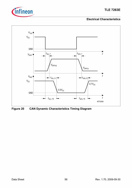
Dynamic CAN-Transceiver CharacteristicsPropagation delayTxD-to-RxD LOW (recessive to dominant)
td(L),TR – 150 255 ns CL = 47 pF;RL = 60 Ω;VCC1/2 = 5 V;CRxD = 20 pF
Propagation delayTxD-to-RxD HIGH (dominant to recessive)
td(H),TR – 150 255 ns CL = 47 pF;RL = 60 Ω;VCC1/2 = 5 V;CRxD = 20 pF
Propagation delayTxD LOW to bus dominant
td(L),T – 50 120 ns CL = 47 pF;RL = 60 Ω;VCC1/2 = 5 V
Propagation delayTxD HIGH to bus recessive
td(H),T – 50 120 ns CL = 47 pF;RL = 60 Ω;VCC1/2 = 5 V
Propagation delaybus dominant to RxD LOW
td(L),R – 100 135 ns CL = 47 pF;RL = 60 Ω;VCC1/2 = 5 V;CRxD = 20 pF
Propagation delaybus recessive to RxD HIGH
td(H),R – 100 135 ns CL = 47 pF;RL = 60 Ω;VCC1/2 = 5 V;CRxD = 20 pF
Min. dominant time for bus wake-up
tWU 1 3 5 μs –
TxD permanent dominant disable time
tTxD 0.3 – 1.0 ms –
Table 13 Electrical Characteristics (cont’d)VS = 13.5 V; ICC1 = 1 mA; 4.9 V < VCC1/2 < 5.1 V; SBC Active Mode; all outputs open;-40 °C < Tj < 150 °C (max. 125 °C for CAN circuit characteristics); all voltages withrespect to ground; positive current defined flowing into pin; unless otherwise specified.
Parameter Symbol Limit Values Unit Test ConditionMin. Typ. Max.
Data Sheet 40 Rev. 1.70, 2009-09-30
TLE 7263E
Electrical Characteristics
LIN Transceiver CharacteristicsReceive Output RxDHIGH level output voltage
VRxD,H 0.8 × VCC1
– – V IRxD(LIN) = -1.6 mA;Vbus = VS
LOW level output voltage
VRxD,L – – 0.2 × VCC1
V IRxD(LIN) = 1.6 mA;Vbus = 0 V
Transmission Input TxDHIGH level input voltage threshold
VTxD,H – – 0.7 × VCC1
V recessive state
TxD input hysteresis VTxD,hys 0.8 1.5 V –LOW level input voltage threshold
VTxD,L 0.3 × VCC1
– – V dominant state
TxD pull-up Resistor RTxD 20 40 80 kΩ VTxD = 0 VBus ReceiverReceiver threshold voltage, recessive to dominant edge
Vbus,rd 0.42 × VS
0.48 × VS
– V –
Receiver dominant state
Vbusdom – – 0.40 × VS
V (LIN Spec 1.3 (2.0);Line 10.1.9 (3.1.9))
Receiver threshold voltage, dominant to recessive edge
Vbus,dr – 0.52 × VS
0.58 × VS
V Vbus,rec < Vbus < 27 V
Receiver recessive state
Vbusrec 0.6 × VS
– – – (LIN Spec 1.3 (2.0);Line 10.1.10 (3.1.10))
Receiver center voltage Vbuscent 0.475 × VS
0.5 × VS
0.525 × VS
V (LIN Spec 1.3 (2.0);Line 10.1.11 (3.1.11))
Receiver hysteresis Vbus,hys 0.02 × VS
0.175 × VS
V Vbus,hys =Vbus,rec - Vbus,dom(LIN Spec 1.3 (2.0);Line 10.1.12 (3.1.12))
Table 13 Electrical Characteristics (cont’d)VS = 13.5 V; ICC1 = 1 mA; 4.9 V < VCC1/2 < 5.1 V; SBC Active Mode; all outputs open;-40 °C < Tj < 150 °C (max. 125 °C for CAN circuit characteristics); all voltages withrespect to ground; positive current defined flowing into pin; unless otherwise specified.
Parameter Symbol Limit Values Unit Test ConditionMin. Typ. Max.
Data Sheet 41 Rev. 1.70, 2009-09-30
TLE 7263E
Electrical Characteristics
Wake-up threshold voltage
Vwake 0.40 × VS
0.5 × VS
0.6 × VS
V –
Bus TransmitterBus serial diode voltage drop
Vserdiode 0.4 0.7 1.0 V VTxD = high Level
Bus dominant output voltage
Vbus,dom – – 1.2 V VTxD = 0 V; VS = 7 V;RL = 500 Ω;(LIN Spec 1.3;Line 10.1.13)
– – 2.0 V VS = 18 V;RL = 500 Ω;(LIN Spec 1.3;Line 10.1.14)
Bus dominant output voltage
Vbus,dom 0.6 – – V VTxD = 0 V; VS = 7 V;RL = 1 kΩ;(LIN Spec 1.3;Line 10.1.15)
0.8 – – V VS = 18 V; RL = 1 kΩ;(LIN Spec 1.3;Line 10.1.16)
Bus short circuit current Ibus,sc 40 100 150 mA Vbus,short = 18 V(LIN Spec 1.3 (2.0);Line 10.1.4 (3.1.4))
Table 13 Electrical Characteristics (cont’d)VS = 13.5 V; ICC1 = 1 mA; 4.9 V < VCC1/2 < 5.1 V; SBC Active Mode; all outputs open;-40 °C < Tj < 150 °C (max. 125 °C for CAN circuit characteristics); all voltages withrespect to ground; positive current defined flowing into pin; unless otherwise specified.
Parameter Symbol Limit Values Unit Test ConditionMin. Typ. Max.
Data Sheet 42 Rev. 1.70, 2009-09-30
TLE 7263E
Electrical Characteristics
Leakage current Ibus,lk -1000 – – μA VS = 0 V; Vbus = -12V(LIN Spec 1.3 (2.0);Line 10.1.7 (3.1.7))
-500 -140 μA VS = 0 V; Vbus = -8V– 10 25 μA VS = 0 V; Vbus = 18 V
(LIN Spec 1.3 (2.0);Line 10.1.8 (3.1.8))
-1 – – mA VS = 18 V; Vbus = 0 V(LIN Spec 1.3 (2.0);Line 10.1.5(3.1.5))
– – 20 μA VBUS =18V VS = 8V(LIN Spec 1.3 (2.0);Line 10.1.6 (3.1.6))
Bus pull-up resistance Rbus 20 30 60 kΩ Active/Standby mode(LIN Spec 1.3 (2.0);Line 10.2.2 (3.2.2))
LIN output current Ilin 5 20 60 μA Sleep mode;Vbus = 0V
Table 13 Electrical Characteristics (cont’d)VS = 13.5 V; ICC1 = 1 mA; 4.9 V < VCC1/2 < 5.1 V; SBC Active Mode; all outputs open;-40 °C < Tj < 150 °C (max. 125 °C for CAN circuit characteristics); all voltages withrespect to ground; positive current defined flowing into pin; unless otherwise specified.
Parameter Symbol Limit Values Unit Test ConditionMin. Typ. Max.
Data Sheet 43 Rev. 1.70, 2009-09-30
TLE 7263E
Electrical Characteristics
Dynamic Transceiver CharacteristicsSlew rate falling edge Sfslope -3 – -1 V/μs 60% > Vbus > 40%
1 μs < (τ = Rl × Cbus)< 5 μs;VS = 18V;Active mode 2)
(LIN Spec 1.3;Line 10.3.1)
Slew rate falling edge Sfslope -3 – -0.5 V/μs 60% > Vbus > 40%1 μs < (τ = Rl × Cbus)< 5 μs;VS = 7V;Active mode 2)
(LIN Spec 1.3;Line 10.3.2)
Slew rate rising edge Srslope 1 – 3 V/μs 40% < Vbus < 60%1 μs < (τ = Rl × Cbus)< 5 μs;VS = 18V;Active mode 2)
(LIN Spec 1.3;Line 10.3.1)
Slew rate rising edge Srslope 0.5 – 3 V/μs 40% < Vbus < 60%1 μs < (τ = Rl × Cbus)< 5 μs;VS = 7V;Active mode. 2)
(LIN Spec 1.3;Line 10.3.2)
Slope symmetry tslopesym -5 – 5 μs tfslope - trslope;VS = 18.0 V 2)
(LIN Spec 1.3;Line 10.3.3)
Table 13 Electrical Characteristics (cont’d)VS = 13.5 V; ICC1 = 1 mA; 4.9 V < VCC1/2 < 5.1 V; SBC Active Mode; all outputs open;-40 °C < Tj < 150 °C (max. 125 °C for CAN circuit characteristics); all voltages withrespect to ground; positive current defined flowing into pin; unless otherwise specified.
Parameter Symbol Limit Values Unit Test ConditionMin. Typ. Max.
Data Sheet 44 Rev. 1.70, 2009-09-30
TLE 7263E
Electrical Characteristics
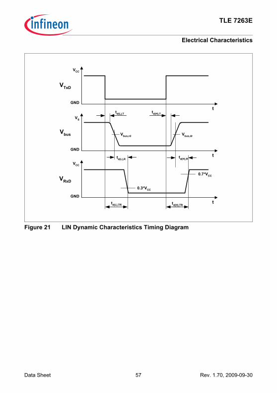
Propagation delayTxD LOW to bus
td(L),T – 1 4 μs (LIN Spec 1.3;Line 10.3.6)2)
Propagation delayTxD HIGH to bus
td(H),T – 1 4 μs (LIN Spec 1.3;Line 10.3.6)2)
Propagation delaybus dominant to RxD LOW
td(L),R – 1 6 μs CRxD = 20 pF;(LIN Spec 1.3;Line 10.3.7)
Propagation delaybus recessive to RxD HIGH
td(H),R – 1 6 μs CRxD = 20 pF;(LIN Spec 1.3;Line 10.3.7)
Receiver delay symmetry
tsym,R -2 – 2 μs tsym,R = td(L),R - td(H),R(LIN Spec 1.3;Line 10.3.8)
Transmitter delay symmetry
tsym,T -2 – 2 μs tsym,T = td(L),T - td(H),T(LIN Spec 1.3;Line 10.3.9)2)
Wake-up delay time twake 30 100 150 μs Tj ≤ 125 °C– – 170 μs Tj ≤ 150 °C
TxD dominant time out ttimeout 6 12 20 ms VTxD = 0 VTxD dominant time out recovery time
ttorec – 10 – μs VTxD = 5 VNot subject to production test. Specified by design
Table 13 Electrical Characteristics (cont’d)VS = 13.5 V; ICC1 = 1 mA; 4.9 V < VCC1/2 < 5.1 V; SBC Active Mode; all outputs open;-40 °C < Tj < 150 °C (max. 125 °C for CAN circuit characteristics); all voltages withrespect to ground; positive current defined flowing into pin; unless otherwise specified.
Parameter Symbol Limit Values Unit Test ConditionMin. Typ. Max.
Data Sheet 45 Rev. 1.70, 2009-09-30
TLE 7263E
Electrical Characteristics
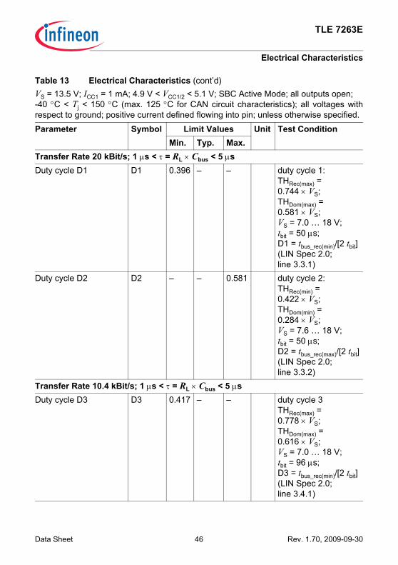
Transfer Rate 20 kBit/s; 1 μs < τ = RL × Cbus < 5 μsDuty cycle D1 D1 0.396 – – duty cycle 1:
THRec(max) =0.744 × VS;THDom(max) =0.581 × VS;VS = 7.0 … 18 V;tbit = 50 μs;D1 = tbus_rec(min)/[2 tbit](LIN Spec 2.0;line 3.3.1)
Duty cycle D2 D2 – – 0.581 duty cycle 2:THRec(min) =0.422 × VS;THDom(min) =0.284 × VS;VS = 7.6 … 18 V;tbit = 50 μs;D2 = tbus_rec(max)/[2 tbit](LIN Spec 2.0;line 3.3.2)
Transfer Rate 10.4 kBit/s; 1 μs < τ = RL × Cbus < 5 μsDuty cycle D3 D3 0.417 – – duty cycle 3
THRec(max) =0.778 × VS;THDom(max) =0.616 × VS;VS = 7.0 … 18 V;tbit = 96 μs;D3 = tbus_rec(min)/[2 tbit](LIN Spec 2.0;line 3.4.1)
Table 13 Electrical Characteristics (cont’d)VS = 13.5 V; ICC1 = 1 mA; 4.9 V < VCC1/2 < 5.1 V; SBC Active Mode; all outputs open;-40 °C < Tj < 150 °C (max. 125 °C for CAN circuit characteristics); all voltages withrespect to ground; positive current defined flowing into pin; unless otherwise specified.
Parameter Symbol Limit Values Unit Test ConditionMin. Typ. Max.
Data Sheet 46 Rev. 1.70, 2009-09-30
TLE 7263E
Electrical Characteristics
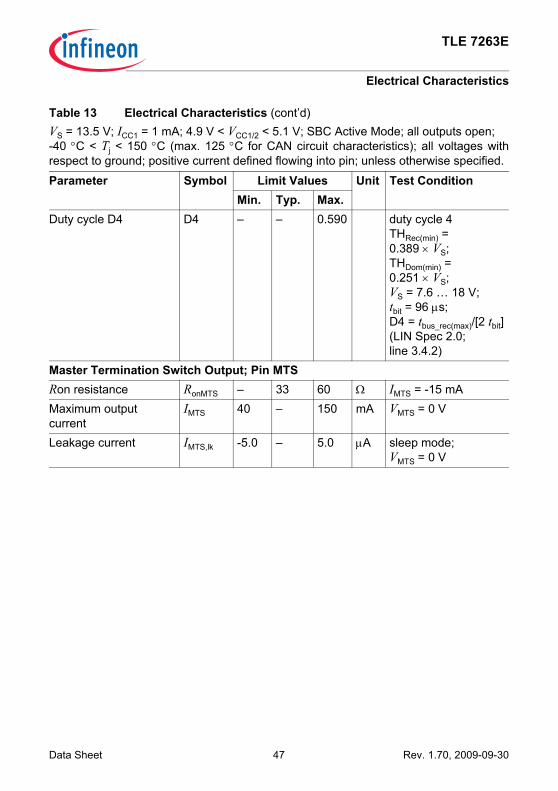
Duty cycle D4 D4 – – 0.590 duty cycle 4THRec(min) =0.389 × VS;THDom(min) =0.251 × VS;VS = 7.6 … 18 V;tbit = 96 μs;D4 = tbus_rec(max)/[2 tbit](LIN Spec 2.0;line 3.4.2)
Master Termination Switch Output; Pin MTSRon resistance RonMTS – 33 60 Ω IMTS = -15 mAMaximum output current
IMTS 40 – 150 mA VMTS = 0 V
Leakage current IMTS,lk -5.0 – 5.0 μA sleep mode;VMTS = 0 V
Table 13 Electrical Characteristics (cont’d)VS = 13.5 V; ICC1 = 1 mA; 4.9 V < VCC1/2 < 5.1 V; SBC Active Mode; all outputs open;-40 °C < Tj < 150 °C (max. 125 °C for CAN circuit characteristics); all voltages withrespect to ground; positive current defined flowing into pin; unless otherwise specified.
Parameter Symbol Limit Values Unit Test ConditionMin. Typ. Max.
Data Sheet 47 Rev. 1.70, 2009-09-30
TLE 7263E
Electrical Characteristics
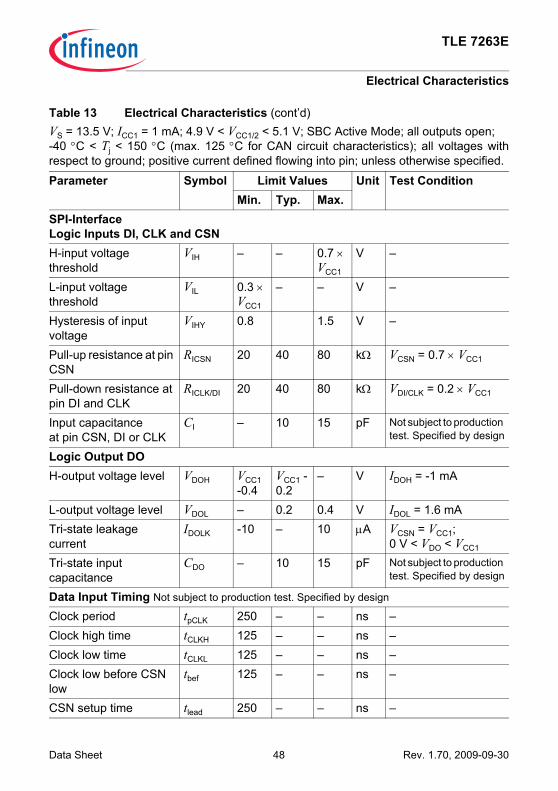
SPI-InterfaceLogic Inputs DI, CLK and CSNH-input voltage threshold
VIH – – 0.7 × VCC1
V –
L-input voltage threshold
VIL 0.3 × VCC1
– – V –
Hysteresis of input voltage
VIHY 0.8 1.5 V –
Pull-up resistance at pin CSN
RICSN 20 40 80 kΩ VCSN = 0.7 × VCC1
Pull-down resistance at pin DI and CLK
RICLK/DI 20 40 80 kΩ VDI/CLK = 0.2 × VCC1
Input capacitanceat pin CSN, DI or CLK
CI – 10 15 pF Not subject to production test. Specified by design
Logic Output DOH-output voltage level VDOH VCC1
-0.4VCC1 -0.2
– V IDOH = -1 mA
L-output voltage level VDOL – 0.2 0.4 V IDOL = 1.6 mATri-state leakage current
IDOLK -10 – 10 μA VCSN = VCC1;0 V < VDO < VCC1
Tri-state input capacitance
CDO – 10 15 pF Not subject to production test. Specified by design
Data Input Timing Not subject to production test. Specified by design
Clock period tpCLK 250 – – ns –Clock high time tCLKH 125 – – ns –Clock low time tCLKL 125 – – ns –Clock low before CSN low
tbef 125 – – ns –
CSN setup time tlead 250 – – ns –
Table 13 Electrical Characteristics (cont’d)VS = 13.5 V; ICC1 = 1 mA; 4.9 V < VCC1/2 < 5.1 V; SBC Active Mode; all outputs open;-40 °C < Tj < 150 °C (max. 125 °C for CAN circuit characteristics); all voltages withrespect to ground; positive current defined flowing into pin; unless otherwise specified.
Parameter Symbol Limit Values Unit Test ConditionMin. Typ. Max.
Data Sheet 48 Rev. 1.70, 2009-09-30
TLE 7263E
Electrical Characteristics
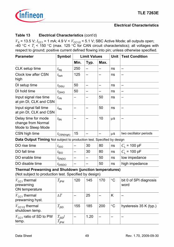
CLK setup time tlag 250 – – ns –Clock low after CSN high
tbeh 125 – – ns –
DI setup time tDISU 50 – – ns –DI hold time tDIHO 50 – – ns –Input signal rise timeat pin DI, CLK and CSN
trIN – – 50 ns –
Input signal fall timeat pin DI, CLK and CSN
tfIN – – 50 ns –
Delay time for mode change from Normal Mode to Sleep Mode
tfIN – – 10 μs –
CSN high time tCSN(high) 15 – – μs two oscillator periods
Data Output Timing Not subject to production test. Specified by design
DO rise time trDO – 30 80 ns CL = 100 pFDO fall time tfDO – 30 80 ns CL = 100 pFDO enable time tENDO – – 50 ns low impedanceDO disable time tDISDO – – 50 ns high impedanceThermal Prewarning and Shutdown (junction temperatures)(Not subject to production test. Specified by design)VCC1 thermal prewarningON temperature
TjPW 120 145 170 °C bit 0 of SPI diagnosis word
VCC1 thermal prewarning hyst.
ΔT – 25 – K –
VCC1/2 thermal shutdown temp.
TjSD 155 185 200 °C hysteresis 35 K (typ.)
VCC1 ratio of SD to PW temp.
TjSD/TjPW
– 1.20 – – –
Table 13 Electrical Characteristics (cont’d)VS = 13.5 V; ICC1 = 1 mA; 4.9 V < VCC1/2 < 5.1 V; SBC Active Mode; all outputs open;-40 °C < Tj < 150 °C (max. 125 °C for CAN circuit characteristics); all voltages withrespect to ground; positive current defined flowing into pin; unless otherwise specified.
Parameter Symbol Limit Values Unit Test ConditionMin. Typ. Max.
Data Sheet 49 Rev. 1.70, 2009-09-30
TLE 7263E
Electrical Characteristics
OUTHS thermal shutdown temp.
TjSD 150 175 200 °C –
OUTHS thermal shutdown hyst.
ΔT – 10 – K –
CAN Transmitter thermal shutdown temp.
TjSD 150 – 190 °C –
CAN Transmitter thermal shutdown hyst.
ΔT – 10 – K –
LIN Transmitter thermal shutdown temp.
TjSD 150 – 190 °C –
LIN Transmitter thermal shutdown hyst.
ΔT – 10 – K –
1) Vdiff = VCANH - VCANL
2) tested at 20kbit/s
Table 13 Electrical Characteristics (cont’d)VS = 13.5 V; ICC1 = 1 mA; 4.9 V < VCC1/2 < 5.1 V; SBC Active Mode; all outputs open;-40 °C < Tj < 150 °C (max. 125 °C for CAN circuit characteristics); all voltages withrespect to ground; positive current defined flowing into pin; unless otherwise specified.
Parameter Symbol Limit Values Unit Test ConditionMin. Typ. Max.
Data Sheet 50 Rev. 1.70, 2009-09-30
TLE 7263E
Electrical Characteristics
Timing Diagrams
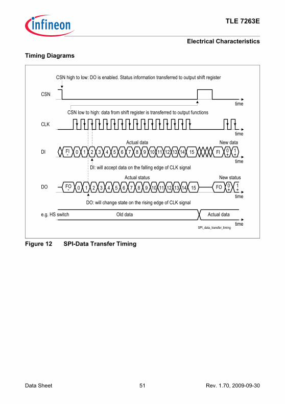
Figure 12 SPI-Data Transfer Timing
0 0+1 2 3 4 5 6 7 8 9 10 15 1
+
0 1 2 3 4 5 6 11 12 13 147 8 9 10 15
FIFI-
CSN high to low: DO is enabled. Status information transferred to output shift register
CSN low to high: data from shift register is transferred to output functions
DI: will accept data on the falling edge of CLK signal
DO: will change state on the rising edge of CLK signal
Actual status
11 12 13 14
Actual data New data
New status
Actual dataOld datae.g. HS switch
DO
DI
CSN
CLK
time
time
time
time
timeSPI_data_transfer_timing
FOFO-0+
1+
Data Sheet 51 Rev. 1.70, 2009-09-30
TLE 7263E
Electrical Characteristics
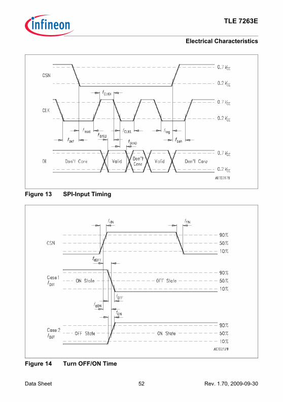
Figure 13 SPI-Input Timing
Figure 14 Turn OFF/ON Time
Data Sheet 52 Rev. 1.70, 2009-09-30
TLE 7263E
Electrical Characteristics
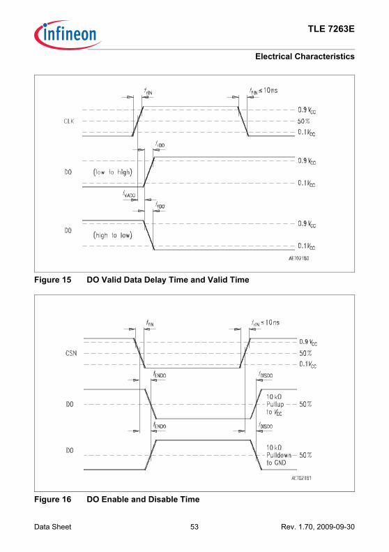
Figure 15 DO Valid Data Delay Time and Valid Time
Figure 16 DO Enable and Disable Time
Data Sheet 53 Rev. 1.70, 2009-09-30
TLE 7263E
Electrical Characteristics
Figure 17 Watchdog Time-Out Definitions
Figure 18 Watchdog Timing Diagram
closed window open window
tCWmin
t / [tWDPER]
tWD
tOWmax
safe trigger area
tCWmax
tOWmin
0.4 1.20.80.6
tWWRP
1.0
tWWRP : Window Watchdog Reset Period set via SPI, see table 9
tWDR
Watchdogtimer reset
normaloperation
timeout(too long)
timeout(too short)
normaloperation
ResetOut
WDTrigger
t
t
normaloperation
tCW tOW tLW tCW tOWtCW+tOW tLW tCW
tCW tOW tCW tOW tLW
Data Sheet 54 Rev. 1.70, 2009-09-30
TLE 7263E
Electrical Characteristics
Figure 19 Reset Timing Diagram
tRD1 tLW
tWDRx
Watchdogtimer reset
start up start up
ResetOut
WDTrigger
t
VCC VRTx
undervoltage
tRDx
normal operation
t
t
tLWtLW
tCW tOW
VCC1-Fail
t < tRR
activation by µC[first SPI transmission]
t
VCC1failflag
LOW
HIGH
tRR
tVCC, r
tCW
Data Sheet 55 Rev. 1.70, 2009-09-30
TLE 7263E
Electrical Characteristics
Figure 20 CAN Dynamic Characteristics Timing Diagram
AET02926
TxDV
VCC
GND
VDIFFd(L), Tt d(H), Tt
VDIFF(d)
DIFF(r)V
t
t
GND
CCV
VRxD
t
d(L), Rt d(H), Rt
CCV0.7
0.3 CCV
d(L), TRt d(H), TRt
Data Sheet 56 Rev. 1.70, 2009-09-30
TLE 7263E
Electrical Characteristics
Figure 21 LIN Dynamic Characteristics Timing Diagram
GND
VTxD
t
VCC
Vbus
t
GND
VRxD
t
VCC
0.3*VCC
0.7*VCC
td(H),Rtd(L),R
td(H),TRtd(L),TR
td(H),Ttd(L),T
Vbus,rd Vbus,dr
VS
GND
Data Sheet 57 Rev. 1.70, 2009-09-30
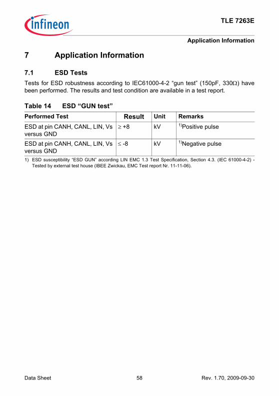
TLE 7263E
Application Information
7 Application Information
7.1 ESD TestsTests for ESD robustness according to IEC61000-4-2 “gun test” (150pF, 330Ω) havebeen performed. The results and test condition are available in a test report.
Table 14 ESD “GUN test”Performed Test Result Unit RemarksESD at pin CANH, CANL, LIN, Vs versus GND
≥ +8 kV 1)Positive pulse
1) ESD susceptibility “ESD GUN” according LIN EMC 1.3 Test Specification, Section 4.3. (IEC 61000-4-2) -Tested by external test house (IBEE Zwickau, EMC Test report Nr. 11-11-06).
ESD at pin CANH, CANL, LIN, Vs versus GND
≤ -8 kV 1)Negative pulse
Data Sheet 58 Rev. 1.70, 2009-09-30
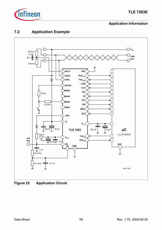
TLE 7263E
Application Information
7.2 Application Example
Figure 22 Application Circuit
VS
Vbat
GND
CANH
CANL
CANbus
WKO
TLE 726368 µF100 nF
GND
µC
DO
TxDCAN
CSN
RO
VCC1
RxDCAN
CLK
VCC2
10 µF
e.g. XC164CM
INT
100 nF
LIN
RxDLIN
TxDLINLINBus 0.1 µF
VCC2
FSO
MON2
SI
OUTHS
10 kOhm
100 kOhm
MON4
MON31kOhm
SPLIT
60Ohms
60Ohms4.7nF
4.7 nF
Appl_7263
MTS
1 kOhm
1 nF
10 µF
MON1
STS
DI
160 kOhm
Data Sheet 59 Rev. 1.70, 2009-09-30
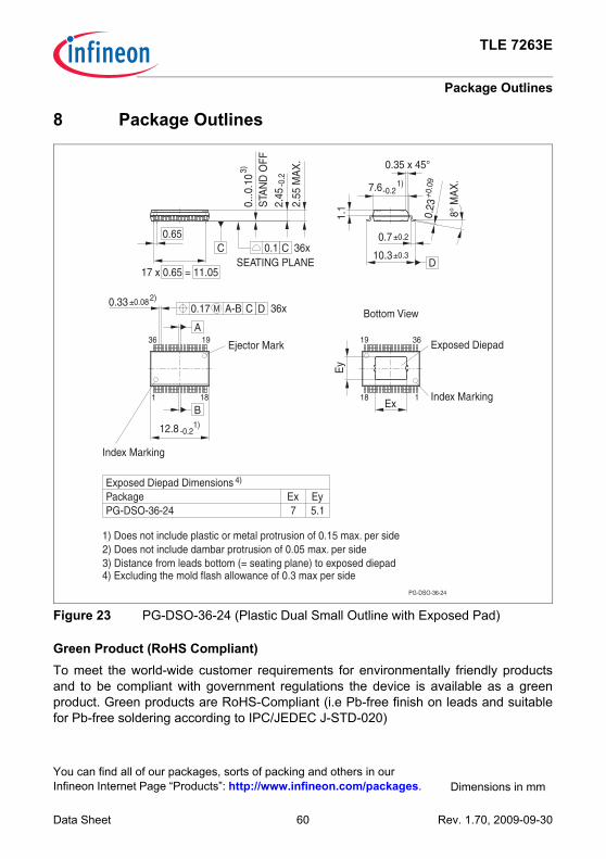
TLE 7263E
Package Outlines
8 Package Outlines
Figure 23 PG-DSO-36-24 (Plastic Dual Small Outline with Exposed Pad)
Green Product (RoHS Compliant)To meet the world-wide customer requirements for environmentally friendly productsand to be compliant with government regulations the device is available as a greenproduct. Green products are RoHS-Compliant (i.e Pb-free finish on leads and suitablefor Pb-free soldering according to IPC/JEDEC J-STD-020)
PG-DSO-36-24
Exposed Diepad
Index Marking
1) Does not include plastic or metal protrusion of 0.15 max. per side2) Does not include dambar protrusion of 0.05 max. per side3) Distance from leads bottom (= seating plane) to exposed diepad
Index Marking
1 18
36 19
18 1
19 36
Bottom View
0.65
17 x 0.65 = 11.05
±0.080.33 2)
3)
A-B0.17 M 36xC
C C
D
0.1 36xSEATING PLANE
0...0
.10
STA
ND
OFF
-0.2
2.45
2.55
MA
X.
1.1
-0.27.6 1)
0.35 x 45°
0.7 ±0.2
10.3±0.3
+0.0
90.
23
8° M
AX
.
A
D
1)12.8 -0.2
B
PG-DSO-36-24Package
7 5.1
Exposed Diepad Dimensions
Ejector Mark
4)
4) Excluding the mold flash allowance of 0.3 max per side
Ex
Ex Ey
Ey
You can find all of our packages, sorts of packing and others in ourInfineon Internet Page “Products”: http://www.infineon.com/packages. Dimensions in mm
Data Sheet 60 Rev. 1.70, 2009-09-30
TLE 7263E
Revision History
9 Revision History
TLE 7263E
Revision History: 2009-09-30 Rev. 1.70
Previous Version: Revision 1.51
Page Subjects (major changes since last revision)2 LIN compatibility to LIN 2.1 and SAE J2602-2 added.35 Added additional line for Sense In threshold voltage, measured at 25°C41 Receiver Hysteresis: Parameter changed to specification of LIN 1.3 43 LIN Leakage Current (first line): Test condition and parameter added
according to specification of LIN1.3, 2.0 and LIN2.144 Slope Symmetry: Test condition updated to specification LIN1.3.44 Slew Rate Falling Edge: Test condition changed to specification LIN1.344 Slew Rate Rising Edge: Test condition changed to specification LIN1.345 Propagation Delay: Test condition changed, tested at 20kbit/s according
LIN1.3 45 Transmitter Delay Symmetry: Test condition changed, tested at 20kbit/s
according LIN1.3 46 Slew Rate Rising and Falling Edge: Parameters for 10.4kBit/s removed 60 Figure 23: Update of Package Outlines drawing with reduced max. stand-
off
Data Sheet 61 Rev. 1.70, 2009-09-30
Edition 2009-09-30Published byInfineon Technologies AG81726 München, Germany© Infineon Technologies AG 2009.All Rights Reserved.
Legal DisclaimerThe information given in this document shall in no event be regarded as a guarantee of conditions or characteristics. With respect to any examples or hints given herein, any typical values stated herein and/or any information regarding the application of the device, Infineon Technologies hereby disclaims any and all warranties and liabilities of any kind, including without limitation, warranties of non-infringement of intellectual property rights of any third party.
InformationFor further information on technology, delivery terms and conditions and prices, please contact the nearest Infineon Technologies Office (www.infineon.com).
WarningsDue to technical requirements, components may contain dangerous substances. For information on the types in question, please contact the nearest Infineon Technologies Office.Infineon Technologies components may be used in life-support devices or systems only with the express written approval of Infineon Technologies, if a failure of such components can reasonably be expected to cause the failure of that life-support device or system or to affect the safety or effectiveness of that device or system. Life support devices or systems are intended to be implanted in the human body or to support and/or maintain and sustain and/or protect human life. If they fail, it is reasonable to assume that the health of the user or other persons may be endangered.